WO2022092105A1 - Method for manufacturing electrode foil for electrolytic capacitor, method for manufacturing electrolytic capacitor, and power supply device - Google Patents
Method for manufacturing electrode foil for electrolytic capacitor, method for manufacturing electrolytic capacitor, and power supply device Download PDFInfo
- Publication number
- WO2022092105A1 WO2022092105A1 PCT/JP2021/039535 JP2021039535W WO2022092105A1 WO 2022092105 A1 WO2022092105 A1 WO 2022092105A1 JP 2021039535 W JP2021039535 W JP 2021039535W WO 2022092105 A1 WO2022092105 A1 WO 2022092105A1
- Authority
- WO
- WIPO (PCT)
- Prior art keywords
- alternating current
- electrolytic capacitor
- waveform data
- etching
- electrode foil
- Prior art date
Links
- 239000011888 foil Substances 0.000 title claims abstract description 77
- 239000003990 capacitor Substances 0.000 title claims abstract description 63
- 238000000034 method Methods 0.000 title claims abstract description 27
- 238000004519 manufacturing process Methods 0.000 title claims abstract description 24
- 238000005530 etching Methods 0.000 claims abstract description 71
- 229910052751 metal Inorganic materials 0.000 claims abstract description 58
- 239000002184 metal Substances 0.000 claims abstract description 58
- 238000003860 storage Methods 0.000 claims description 16
- 239000007784 solid electrolyte Substances 0.000 claims description 15
- 230000015572 biosynthetic process Effects 0.000 claims description 9
- 238000003786 synthesis reaction Methods 0.000 claims description 8
- 239000000243 solution Substances 0.000 description 17
- VEXZGXHMUGYJMC-UHFFFAOYSA-N Hydrochloric acid Chemical compound Cl VEXZGXHMUGYJMC-UHFFFAOYSA-N 0.000 description 8
- 238000000866 electrolytic etching Methods 0.000 description 8
- 238000000605 extraction Methods 0.000 description 7
- NBIIXXVUZAFLBC-UHFFFAOYSA-N Phosphoric acid Chemical compound OP(O)(O)=O NBIIXXVUZAFLBC-UHFFFAOYSA-N 0.000 description 6
- QAOWNCQODCNURD-UHFFFAOYSA-N Sulfuric acid Chemical compound OS(O)(=O)=O QAOWNCQODCNURD-UHFFFAOYSA-N 0.000 description 6
- 229910052782 aluminium Inorganic materials 0.000 description 6
- XAGFODPZIPBFFR-UHFFFAOYSA-N aluminium Chemical compound [Al] XAGFODPZIPBFFR-UHFFFAOYSA-N 0.000 description 6
- 229920001940 conductive polymer Polymers 0.000 description 6
- 239000007864 aqueous solution Substances 0.000 description 5
- 229920006351 engineering plastic Polymers 0.000 description 5
- OKTJSMMVPCPJKN-UHFFFAOYSA-N Carbon Chemical compound [C] OKTJSMMVPCPJKN-UHFFFAOYSA-N 0.000 description 4
- 238000004140 cleaning Methods 0.000 description 4
- 238000012986 modification Methods 0.000 description 4
- 230000004048 modification Effects 0.000 description 4
- 230000001681 protective effect Effects 0.000 description 4
- 229910018072 Al 2 O 3 Inorganic materials 0.000 description 3
- MUBZPKHOEPUJKR-UHFFFAOYSA-N Oxalic acid Chemical compound OC(=O)C(O)=O MUBZPKHOEPUJKR-UHFFFAOYSA-N 0.000 description 3
- 229910000147 aluminium phosphate Inorganic materials 0.000 description 3
- 238000007743 anodising Methods 0.000 description 3
- 229910052799 carbon Inorganic materials 0.000 description 3
- 238000006243 chemical reaction Methods 0.000 description 3
- 230000000052 comparative effect Effects 0.000 description 3
- 239000011810 insulating material Substances 0.000 description 3
- 229920005989 resin Polymers 0.000 description 3
- 239000011347 resin Substances 0.000 description 3
- GRYLNZFGIOXLOG-UHFFFAOYSA-N Nitric acid Chemical compound O[N+]([O-])=O GRYLNZFGIOXLOG-UHFFFAOYSA-N 0.000 description 2
- BQCADISMDOOEFD-UHFFFAOYSA-N Silver Chemical compound [Ag] BQCADISMDOOEFD-UHFFFAOYSA-N 0.000 description 2
- 239000002253 acid Substances 0.000 description 2
- 150000007513 acids Chemical class 0.000 description 2
- 239000000654 additive Substances 0.000 description 2
- VSCWAEJMTAWNJL-UHFFFAOYSA-K aluminium trichloride Chemical compound Cl[Al](Cl)Cl VSCWAEJMTAWNJL-UHFFFAOYSA-K 0.000 description 2
- 230000007423 decrease Effects 0.000 description 2
- 238000010586 diagram Methods 0.000 description 2
- 239000007788 liquid Substances 0.000 description 2
- 229910021645 metal ion Inorganic materials 0.000 description 2
- 150000002739 metals Chemical class 0.000 description 2
- 239000000203 mixture Substances 0.000 description 2
- 229910017604 nitric acid Inorganic materials 0.000 description 2
- TWNQGVIAIRXVLR-UHFFFAOYSA-N oxo(oxoalumanyloxy)alumane Chemical compound O=[Al]O[Al]=O TWNQGVIAIRXVLR-UHFFFAOYSA-N 0.000 description 2
- 230000000379 polymerizing effect Effects 0.000 description 2
- 229910052709 silver Inorganic materials 0.000 description 2
- 239000004332 silver Substances 0.000 description 2
- 230000002194 synthesizing effect Effects 0.000 description 2
- 229920001187 thermosetting polymer Polymers 0.000 description 2
- XLYOFNOQVPJJNP-UHFFFAOYSA-N water Substances O XLYOFNOQVPJJNP-UHFFFAOYSA-N 0.000 description 2
- 239000004640 Melamine resin Substances 0.000 description 1
- 229920000877 Melamine resin Polymers 0.000 description 1
- 239000004962 Polyamide-imide Substances 0.000 description 1
- 239000004642 Polyimide Substances 0.000 description 1
- RTAQQCXQSZGOHL-UHFFFAOYSA-N Titanium Chemical compound [Ti] RTAQQCXQSZGOHL-UHFFFAOYSA-N 0.000 description 1
- 229920001807 Urea-formaldehyde Polymers 0.000 description 1
- 239000000853 adhesive Substances 0.000 description 1
- 230000001070 adhesive effect Effects 0.000 description 1
- 229920000180 alkyd Polymers 0.000 description 1
- 229910045601 alloy Inorganic materials 0.000 description 1
- 239000000956 alloy Substances 0.000 description 1
- HSFWRNGVRCDJHI-UHFFFAOYSA-N alpha-acetylene Natural products C#C HSFWRNGVRCDJHI-UHFFFAOYSA-N 0.000 description 1
- 239000003575 carbonaceous material Substances 0.000 description 1
- 239000002738 chelating agent Substances 0.000 description 1
- 239000002131 composite material Substances 0.000 description 1
- 238000009792 diffusion process Methods 0.000 description 1
- 239000006185 dispersion Substances 0.000 description 1
- 239000002019 doping agent Substances 0.000 description 1
- 239000003792 electrolyte Substances 0.000 description 1
- 239000008151 electrolyte solution Substances 0.000 description 1
- 239000003822 epoxy resin Substances 0.000 description 1
- 229910002804 graphite Inorganic materials 0.000 description 1
- 239000010439 graphite Substances 0.000 description 1
- 239000012535 impurity Substances 0.000 description 1
- 238000009413 insulation Methods 0.000 description 1
- 239000012774 insulation material Substances 0.000 description 1
- 229910000765 intermetallic Inorganic materials 0.000 description 1
- 150000002697 manganese compounds Chemical class 0.000 description 1
- 239000000463 material Substances 0.000 description 1
- 239000000155 melt Substances 0.000 description 1
- 238000002844 melting Methods 0.000 description 1
- 230000008018 melting Effects 0.000 description 1
- 239000000178 monomer Substances 0.000 description 1
- 229910052758 niobium Inorganic materials 0.000 description 1
- 239000010955 niobium Substances 0.000 description 1
- GUCVJGMIXFAOAE-UHFFFAOYSA-N niobium atom Chemical compound [Nb] GUCVJGMIXFAOAE-UHFFFAOYSA-N 0.000 description 1
- 235000006408 oxalic acid Nutrition 0.000 description 1
- 239000002245 particle Substances 0.000 description 1
- 239000005011 phenolic resin Substances 0.000 description 1
- 229920000172 poly(styrenesulfonic acid) Polymers 0.000 description 1
- 229920001197 polyacetylene Polymers 0.000 description 1
- 229920002312 polyamide-imide Polymers 0.000 description 1
- 229920000767 polyaniline Polymers 0.000 description 1
- 229920000647 polyepoxide Polymers 0.000 description 1
- 229920001721 polyimide Polymers 0.000 description 1
- 229920000128 polypyrrole Polymers 0.000 description 1
- 229940005642 polystyrene sulfonic acid Drugs 0.000 description 1
- 229920000123 polythiophene Polymers 0.000 description 1
- 229920002635 polyurethane Polymers 0.000 description 1
- 239000004814 polyurethane Substances 0.000 description 1
- 239000011148 porous material Substances 0.000 description 1
- 239000002994 raw material Substances 0.000 description 1
- 238000007789 sealing Methods 0.000 description 1
- 229920002050 silicone resin Polymers 0.000 description 1
- 239000000126 substance Substances 0.000 description 1
- 229910052715 tantalum Inorganic materials 0.000 description 1
- GUVRBAGPIYLISA-UHFFFAOYSA-N tantalum atom Chemical compound [Ta] GUVRBAGPIYLISA-UHFFFAOYSA-N 0.000 description 1
- 238000010998 test method Methods 0.000 description 1
- 229910052719 titanium Inorganic materials 0.000 description 1
- 239000010936 titanium Substances 0.000 description 1
- 229920006305 unsaturated polyester Polymers 0.000 description 1
- 238000003466 welding Methods 0.000 description 1
- 238000004804 winding Methods 0.000 description 1
Images


Classifications
-
- C—CHEMISTRY; METALLURGY
- C25—ELECTROLYTIC OR ELECTROPHORETIC PROCESSES; APPARATUS THEREFOR
- C25F—PROCESSES FOR THE ELECTROLYTIC REMOVAL OF MATERIALS FROM OBJECTS; APPARATUS THEREFOR
- C25F3/00—Electrolytic etching or polishing
- C25F3/02—Etching
-
- C—CHEMISTRY; METALLURGY
- C25—ELECTROLYTIC OR ELECTROPHORETIC PROCESSES; APPARATUS THEREFOR
- C25F—PROCESSES FOR THE ELECTROLYTIC REMOVAL OF MATERIALS FROM OBJECTS; APPARATUS THEREFOR
- C25F3/00—Electrolytic etching or polishing
- C25F3/02—Etching
- C25F3/04—Etching of light metals
-
- H—ELECTRICITY
- H01—ELECTRIC ELEMENTS
- H01G—CAPACITORS; CAPACITORS, RECTIFIERS, DETECTORS, SWITCHING DEVICES OR LIGHT-SENSITIVE DEVICES, OF THE ELECTROLYTIC TYPE
- H01G9/00—Electrolytic capacitors, rectifiers, detectors, switching devices, light-sensitive or temperature-sensitive devices; Processes of their manufacture
Definitions
- the present invention relates to a method for manufacturing an electrode foil for an electrolytic capacitor, a method for manufacturing an electrolytic capacitor, and a power supply device.
- the electrolytic capacitor is equipped with a capacitor element.
- a metal foil containing a valve acting metal is used as the anode body of the capacitor element.
- all or part of the main surface of the metal leaf is etched. Etching is performed by applying an alternating current to the metal foil in the etching solution.
- Patent Documents 1 and 2 propose to make the waveform into a specific shape in an alternating current that repeats one type of waveform.
- the alternating current contains two half-waves having the same or different waveforms, amplitudes, and application times, or all of them, in the positive and negative half cycles. It is proposed to provide a rest period between each half wave in which the amplitude is 0 or the positive or negative side is applied with a minute current within 1/15 of the maximum amplitude.
- Patent Document 2 proposes that the waveform in a positive half cycle includes a portion in which the waveform greatly decreases from the peak time and a portion in which the waveform rises or falls gradually or gradually from immediately after the end of the decrease to the end of the half cycle. ..
- One aspect of the present invention includes an etching step of applying an alternating current to a metal foil in an etching solution to obtain an electrode foil having a porous portion on the surface, and the alternating current has at least two types of waveforms different from each other.
- the present invention relates to a method for manufacturing an electrode foil for an electrolytic capacitor, including.
- Another aspect of the present invention is a step provided in the above-mentioned method for manufacturing an electrode foil for an electrolytic capacitor, a step of covering the porous portion with a dielectric layer, and a step of covering at least a part of the dielectric layer with a solid electrolyte layer. It relates to a process and a method of manufacturing an electrolytic capacitor, including.
- Yet another aspect of the present invention is a power supply device that applies an alternating current to the metal foil in the etching solution in the metal foil etching step, and includes an output unit that outputs the alternating current. It relates to a power supply device containing at least two types of waveforms that are different from each other.
- a good etching pit can be formed on the metal foil.
- the method for producing an electrode foil according to an embodiment of the present invention includes an etching step of applying an alternating current to a metal foil in an etching solution to obtain an electrode foil having a porous portion on the surface.
- Alternating current includes at least two different waveforms that differ from each other. Note that the different waveforms here mean that the shape and / or magnitude of the waves are different.
- the starting point where the pit is generated can be dispersed on the surface of the metal foil, and the pit is localized in the portion where the protective film is thin.
- the formation can be suppressed. That is, the pits can be formed more uniformly on the surface of the metal foil.
- one waveform has a period Tw and a fluctuation range, and includes a positive half period and a negative half period.
- the positive half-cycle shape and the negative half-cycle shape may have a point-symmetrical relationship with each other.
- the fluctuation range corresponds to the sum of the maximum value of the current density in the positive half cycle and the maximum value (absolute value) of the current density in the negative half cycle.
- the maximum values of the current densities existing in the positive and negative half cycles may be the same as each other.
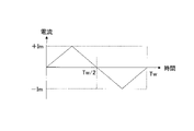
- Examples of the wave shape include a sine wave shown in FIG. 1, a triangular wave shown in FIG. 2, a rectangular wave, and the like.
- Im indicates the maximum value of the current density
- Tw indicates the period.
- 2 ⁇ Im corresponds to the fluctuation width
- Im corresponds to the amplitude.
- At least two types of waveforms may have different fluctuation widths and / or periods from each other. At least two types of waveforms may differ from each other in the maximum value of the current density in the positive half cycle and / or the maximum value of the current density in the negative half cycle.
- At least two types of waveforms may have the same fluctuation width and period, and may have different shapes.
- the timing at which the current density becomes maximum in one cycle may be different.
- the alternating current is a modulated wave containing at least two types of waveforms that are different from each other, and the modulated wave may be repeated with a predetermined period Tm.
- the period Tm of the modulated wave is preferably a value obtained by summing the periods Tw of a plurality of waves (for example, 2 or more and 400 or less).
- the period Tm is preferably an integral multiple of the period Tw, and may be, for example, twice or more and 400 times or less of the period Tw, and may be twice or more and 100 times or less. May be good.
- the fluctuation range may change periodically.
- the maximum value of the current density may be changed into a sinusoidal shape, a triangular wave shape, or a sawtooth wave shape, as shown in FIGS. 3 to 5 described later, for example.
- the period Tm of the modulated wave may be constant, and the fluctuation range may change periodically.
- the ratio of the minimum value A min of the fluctuation width to the maximum value A max of the fluctuation width: A min / A max may be 0.5 or more, and is 0. It may be 6.6 or more, or 0.7 or more.
- a min / A max may be 0.99 or less, 0.97 or less, or 0.9 or less.
- the upper limit and the lower limit of the above A min / A max may be arbitrarily combined.
- a min / A max may be 0.5 or more and 0.99 or less, 0.5 or more and 0.97 or less, and 0.6 or more and 0.97 or less. It may be 0.7 or more and 0.97 or less.
- the maximum value of the current density may be, for example, 5 A / cm 2 or less. Further, when the pit is large, the maximum value of the current density may be 3 A / cm 2 or less.
- the period Tw may be changed periodically.
- the frequency (1 / Tw) is preferably 3 Hz or higher and 65 Hz or lower, for example.
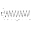
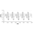
- FIGS. 3 to 5 are graphs showing examples of alternating current modulated waves in the electrolytic etching step in the method for manufacturing an electrode foil for an electrolytic capacitor according to an embodiment of the present invention, respectively.
- the vertical axis is the current density.
- the modulated wave of FIGS. 3 to 5 is obtained by synthesizing the first waveform data shown in FIG. 7 with the second waveform data of FIGS. 8 to 10.
- the current density on the vertical axis of FIGS. 3 to 5 is represented as a relative value when the maximum value of the current density of the first waveform data of FIG. 7 is 1.
- the horizontal axis is time (seconds), and represents, for example, the time from the start of etching.
- the alternating current shown in FIGS. 3 to 5 is a triangular wave, the period Tw is constant, and the fluctuation range changes periodically.
- the alternating current in FIG. 3 includes eight types of waveforms different from each other, the maximum value of the current density changes in a sinusoidal shape, and Tm is eight times Tw.
- the ratio of the minimum value A min of the fluctuation width to the maximum value A max of the fluctuation width: A min / A max is about 0.55.
- the alternating current in FIG. 4 includes two types of waveforms having different fluctuation widths, the maximum value of the current density changes in a triangular wave shape, and Tm is twice Tw.
- the ratio of the minimum value A min of the fluctuation width to the maximum value A max of the fluctuation width: A min / A max is about 0.77.
- the alternating current in FIG. 5 includes three types of waveforms having different fluctuation widths, the maximum value of the current density changes in a sawtooth shape, and Tm is three times Tw.
- the ratio of the minimum value A min of the fluctuation width to the maximum value A max of the fluctuation width: A min / A max is about 0.77.
- Tm / Tw is not limited to the above values.
- Tm / Tw is preferably 2 or more and 100 or less, and preferably 2 or more and 80 or less.
- 1 / Tm is preferably 0.2 Hz or more and 100 Hz or less, and more preferably 0.5 Hz or more and 50 Hz or less.
- the frequency (1 / Tw) is about 24 Hz, but is not limited thereto.
- the frequency (1 / Tw) is, for example, 4 Hz or more and 60 Hz or less, preferably 5 Hz or more and 55 Hz or less.
- a min / A max is not limited to the above numerical values. In the case of the modulated wave of FIG. 3, A min / A max may be 0.55 or more and 0.99 or less, and may be 0.6 or more and 0.97 or less. In the case of the modulated wave of FIGS. 4 and 5, A min / A max may be 0.6 or more and 0.99 or less, and may be 0.7 or more and 0.97 or less.
- Etching of the metal leaf is performed by passing the above-mentioned AC current between the metal leaf and the electrode in the etching solution with the electrode facing the at least one main surface of the metal leaf. Etching may be performed on only one main surface of the metal leaf or on both main surfaces.
- the current density and etching time of the alternating current are not particularly limited, and may be appropriately set according to the thickness of the electrode foil, the desired depth of the etching pit, and the like.
- the average current density of the alternating current applied in the etching step may be constant.
- the average current density of the alternating current is, for example, 0.05 A / cm 2 or more and 1.7 A / cm 2 or less, preferably 0.08 A / cm 2 or more and 1.2 A / cm 2 or less.
- the average current density is obtained by dividing the integrated value of the current density by the time in the current density profile with respect to time.
- the integrated value of the current density in the period Tm is obtained, and the integrated value is divided by Tm to obtain the integrated value.
- the average current density is (2 / ⁇ ) ⁇ Im.
- the average current density is 1/2 ⁇ Im.
- the etching of the metal foil may be performed intermittently.
- the electrolytic etching step preferably has an electroless time.
- the electroless time is, for example, the time for the metal foil to move between the electrodes when there are a plurality of electrodes, and the time for the metal leaf to move between the etching tanks when there are a plurality of etching tanks.
- the electroless time may also be a cleaning step of cleaning the metal leaf.
- Pure water ion-exchanged water
- the cleaning step may be performed during the etching.
- the metal leaf contains valve acting metals such as titanium, tantalum, aluminum and niobium.
- the metal leaf contains one or more of the above valve acting metals.
- the metal leaf may contain the above-mentioned valve acting metal in the form of an alloy or an intermetallic compound.
- the thickness of the metal foil is not particularly limited. The thickness of the metal foil is, for example, 10 ⁇ m or more and 300 ⁇ m or less. When the metal foil is used as the anode foil, the thickness of the metal foil is preferably 60 ⁇ m or more and 250 ⁇ m or less. When the metal foil is used as the cathode foil, the thickness of the metal foil is preferably 10 ⁇ m or more and 80 ⁇ m or less.
- etching solution As the etching solution, a known etching solution used for electrolytic etching can be used. Examples of the etching solution include an aqueous solution containing sulfuric acid, nitric acid, phosphoric acid and / or oxalic acid and hydrochloric acid.
- the aqueous solution may contain various additives such as a chelating agent.
- concentration of hydrochloric acid in the etching solution, the concentration of other acids, and the temperature are not particularly limited, and may be appropriately set according to the desired shape of the etching pit and the performance of the capacitor.
- the concentration of hydrochloric acid in the etching solution is, for example, 1 mol / L or more and 10 mol / L or less.
- the concentration of other acids in the etching solution is, for example, 0.01 mol / L or more and 1 mol / L or less.
- the temperature of the etching solution during the electrolytic etching step is not particularly limited, and is, for example, 5 ° C. or higher and 60 ° C. or lower.
- the power supply device includes an output unit that outputs an alternating current with respect to a power supply device that applies an alternating current to the metal foil in the etching solution in the metal foil etching step, and the alternating currents are mutually exclusive. Includes at least two different waveforms.
- FIG. 6 is a configuration diagram schematically showing an example of a power supply device that outputs an alternating current.
- the power supply device 200 shown in FIG. 6 has a waveform storage unit 201 that stores the first waveform data of the first alternating current, a modulation storage unit 202 that stores the second waveform data that modulates the first waveform data, and a first waveform. It includes a synthesis unit 203 that synthesizes data and a second waveform data, and an output unit 204 that outputs an alternating current as a modulated wave based on the synthesis data synthesized by the synthesis unit 203.
- the second waveform data is data indicating the degree of modulation of the current density (maximum value), fluctuation width, period, etc. with respect to the first waveform data.
- the waveform storage unit 201 stores, for example, the first waveform data of the first alternating current shown in FIG. 7.
- FIG. 7 shows waveform data in which a constant triangular wave is repeated.
- the vertical axis represents the current density, and is represented as a relative value with the maximum value of the current density being 1.
- the horizontal axis is time (seconds).
- the modulation storage unit 202 stores, for example, the second waveform data shown in FIGS. 8 to 10.
- the horizontal axis is time (seconds).
- the vertical axis represents the degree of modulation, which indicates the degree of modulation of the current density of the first waveform data in FIG. 7.
- the current density of the first waveform data is I and the modulation degree is f at an arbitrary time
- the current density after modulation is I ⁇ (1 + a ⁇ f). It becomes.
- the degree of modulation varies from -1 to 1 in a sinusoidal manner.
- a is a coefficient, and is set in the range of, for example, 0.01 to 0.3.
- the degree of modulation f is 0, the current density is the same as the current density in FIG. 7.
- the degree of modulation f is 1 and the coefficient a is 0.3
- the current density (absolute value) is 30% larger than the current density (absolute value) of the first waveform data in FIG. 7.
- the degree of modulation f is -1 and the coefficient a is 0.3
- the current density (absolute value) is 30% smaller than the current density (absolute value) of the first waveform data in FIG. 7.
- the coefficient a is 0.3, the modulated wave of FIG. 3 is obtained.
- the current density of the first waveform data is I and the degree of modulation is f at an arbitrary time
- the current density after modulation is I ⁇ (1 + a).
- the degree of modulation varies between 0 and 1
- the degree of modulation varies between -1 and 0.
- a is a coefficient, and is set in the range of, for example, 0.01 to 0.3.
- the degree of modulation f is 0, the current density is the same as the current density in FIG. 7.
- the current density is 30% larger than the current density of the first waveform data (positive half cycle) in FIG. 7.
- the degree of modulation f is -1 and the coefficient a is 0.3
- the current density (absolute value) with respect to the current density (absolute value) of the first waveform data (negative half cycle) in FIG. Absolute value) increases by 30%.
- the coefficient a is 0.3, the modulated wave of FIGS. 4 and 5 is obtained.
- the fluctuation width of the modulated wave changes periodically, and the ratio of the minimum fluctuation width A min to the maximum fluctuation width A max :
- a min / A max may be within the above range, and is 0. It may be 5.5 or more and 0.97 or less. In this case, good etching pits can be efficiently formed.
- waveform storage unit and the modulation storage unit are provided inside the power supply device in FIG. 6, they may be provided outside the power supply device.
- the power supply device is divided into a synthesis unit that synthesizes the first waveform data of the first alternating current and the second waveform data of the second alternating current whose waveform is different from that of the first alternating current, and the composite data synthesized by the synthesis unit. Based on this, an output unit that outputs an alternating current as a modulated wave may be provided.
- the first alternating current and the second alternating current have different periods or periods and fluctuation ranges from each other, for example.
- the power supply device may include a storage unit that stores waveform data of the first alternating current and the second alternating current. The storage unit may be provided outside the power supply device.
- FIG. 11 is an explanatory diagram schematically showing an example of an etching apparatus used in the etching process.
- the etching apparatus 20 includes an etching tank 23 for holding an etching solution, a plurality of transport rolls 25 for transporting the metal foil 10, a pair of electrodes 22 facing the metal foil 10, and an AC power supply 24 for passing a current through the electrodes 22. , Equipped with.
- the above power supply device for example, the power supply device 200
- the metal leaf 10 moves in the etching tank 23 while being conveyed via the plurality of conveying rolls 25.
- the metal leaf 10 is etched while facing the electrode 22 in the etching tank 23.
- the electrode foil 11 is obtained.
- FIG. 11 shows a case where etching is performed on a long metal foil, but the present invention is not limited to this.
- etching may be performed on a metal leaf having a certain area that has been stationary.
- a pair of electrodes is used, but the present invention is not limited to this.
- the metal leaf may be opposed to one electrode, and the electrode and the metal leaf may be connected to an AC power source for etching.
- the etching device may be provided with a plurality of power supply devices.
- the etching apparatus may include a plurality of etching tanks, and a power supply device may be connected to each of the plurality of etching tanks.
- at least one of the plurality of power supply devices may output an alternating current as a modulated wave, and it is preferable that 20% or more of the plurality of power supply devices output an alternating current as a modulated wave.
- a power supply device is connected to each of 10 or more etching tanks, it is preferable that two or more power supply devices output an alternating current as a modulated wave.
- the method for manufacturing an electrolytic capacitor according to an embodiment of the present invention includes a step (etching step) provided in the above-mentioned method for manufacturing an electrode foil for an electrolytic capacitor, a step of covering a porous portion with a dielectric layer, and a dielectric layer. It comprises a step of covering at least a part with a solid electrolyte layer.
- the dielectric layer may contain oxides of the valve acting metal.
- the dielectric layer may contain Al 2 O 3 .
- the dielectric layer is formed by, for example, anodizing the surface of an anode body (the above-mentioned electrode foil) by chemical conversion treatment or the like.
- the dielectric layer is not limited to this, and may be any one that functions as a dielectric.
- the dielectric layer may be formed so as to cover at least a part of the surface of the anode.
- the dielectric layer is formed along the inner wall surface of the pores and pits of the porous portion of the electrode foil.
- the solid electrolyte layer contains, for example, a manganese compound or a conductive polymer.
- the solid electrolyte layer containing the conductive polymer can be formed, for example, by chemically polymerizing and / or electrolytically polymerizing the raw material monomer on the dielectric layer. Alternatively, it can be formed by applying a solution in which the conductive polymer is dissolved or a dispersion liquid in which the conductive polymer is dispersed to the dielectric layer.
- the conductive polymer polypyrrole, polyaniline, polythiophene, polyacetylene, derivatives thereof and the like can be used.
- the solid electrolyte layer may contain a dopant such as polystyrene sulfonic acid together with the conductive polymer.
- the solid electrolyte layer may further contain additives, if necessary.
- the method for manufacturing an electrolytic capacitor may further include a step of covering the solid electrolyte layer with a cathode extraction layer.
- a capacitor element including an electrode foil, a dielectric layer, a solid electrolyte layer, and a cathode extraction layer may be formed.
- the cathode extraction layer may be formed so as to cover at least a part of the solid electrolyte layer, or may be formed so as to cover the entire surface of the solid electrolyte layer.
- the cathode extraction layer has, for example, a carbon layer and a metal (for example, silver) paste layer formed on the surface of the carbon layer.
- the carbon layer is composed of a composition containing a conductive carbon material such as graphite.
- the metal paste layer is composed of, for example, a composition containing silver particles and a resin.
- the configuration of the cathode extraction layer is not limited to this, and may be any configuration having a current collecting function.
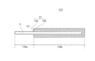
- FIG. 12 is a cross-sectional view schematically showing the capacitor element according to the present embodiment.
- the capacitor element 110 is in the form of a sheet.
- the anode portion 110a is composed of an electrode foil (anode body) 11.
- the cathode portion 110b includes an anode body 11, a dielectric layer 12, and a cathode layer 13.
- the cathode layer 13 has a solid electrolyte layer 13a and a cathode extraction layer 13b.
- the capacitor element constitutes an electrolytic capacitor.
- the electrolytic capacitor may include a plurality of capacitor elements.
- a plurality of capacitor elements may be laminated.
- the number of laminated capacitor elements is not particularly limited, and is, for example, 2 or more and 20 or less.
- the anode parts of the laminated capacitor elements are joined by welding and / or caulking, etc., and are electrically connected.
- An anode lead terminal is bonded to the anode portion of at least one capacitor element.
- the plurality of anode portions are crimped by, for example, bent anode lead terminals.
- the anode portion and the anode lead terminal may be further laser welded. This improves the connection reliability between the plurality of anode portions and the connection reliability between the anode portions and the anode lead terminals.
- the cathode parts of the laminated capacitor elements are also electrically connected to each other.
- a cathode lead terminal is bonded to the cathode layer of at least one capacitor element.
- the cathode lead terminal is bonded to the cathode layer via, for example, a conductive adhesive.
- the capacitor element is sealed with an insulating material so that at least a part of the anode lead terminal and the cathode lead terminal is exposed.
- the insulating material include a cured product of a thermosetting resin and engineering plastics.
- thermosetting resin include epoxy resin, phenol resin, silicone resin, melamine resin, urea resin, alkyd resin, polyurethane, and unsaturated polyester.
- Engineering plastics include general purpose engineering plastics and super engineering plastics. Examples of engineering plastics include polyimide and polyamide-imide.
- FIG. 13 is a cross-sectional view schematically showing an electrolytic capacitor according to this embodiment.
- the electrolytic capacitor 100 includes one or more capacitor elements 110, an anode lead terminal 120A bonded to the anode portion 110a of the capacitor element 110, a cathode lead terminal 120B bonded to the cathode portion 110b, and insulation for sealing the capacitor element.
- the material 130 is provided.
- an electrolytic capacitor in which a solid electrolyte is used as an electrolyte and the capacitor element is sealed with an insulating material is mentioned, but the present invention is not limited to this.
- the electrode foil according to the present embodiment can be applied to, for example, an electrolytic capacitor having an anode and a cathode formed of a strip-shaped electrode foil wound around a separator and an electrolytic solution.
- the electrode foil according to this embodiment is used for at least one of the anode and the cathode.
- the electrode foil according to the present embodiment is preferably used for the anode of a large-capacity laminated electrolytic capacitor or a wound electrolytic capacitor.
- each capacitor element may be of a winding type.
- Examples 1 to 3 An aluminum foil having a thickness of 100 ⁇ m and a purity of 99.98% was prepared. This aluminum foil was immersed in an aqueous solution having a phosphoric acid concentration of 1.0% by mass and 90 ° C. for 60 seconds for pretreatment.
- electrolytic etching was performed as follows using an etching apparatus as shown in FIG.
- As the etching solution an aqueous solution containing 5% by mass of hydrochloric acid, 2% by mass of aluminum chloride, 0.1% by mass of sulfuric acid, 0.5% by mass of phosphoric acid, and 0.2% by mass of nitric acid was used, and the solution temperature was 35 ° C.
- the etching time was 5 minutes.
- the power supply device shown in FIG. 6 was used as the AC power supply.
- the waveform data shown in Table 1 was used for the first waveform data and the second waveform data, and the modulated waves shown in Table 1 were obtained.
- the etching time was 2 minutes.
- the frequency of the alternating current (1 / Tw) was set to about 24 Hz.
- the average current density of the alternating current was constant and was set to 0.2 A / cm 2 .
- the aluminum foil was immersed in an aqueous solution at 60 ° C. containing 10% by mass of sulfuric acid for 60 seconds, and then heat-treated at 250 ° C. for 120 seconds to prepare an electrode foil for an electrolytic capacitor. Further, by anodizing, a dielectric layer containing aluminum oxide (Al 2 O 3 ) was formed on the surface of the electrode foil.
- Comparative Example 1 An electrode foil was obtained in the same manner as in Example 1 except that the first alternating current of the first waveform data was output as it was without synthesizing the first waveform data and the second waveform data. By anodizing, a dielectric layer containing aluminum oxide (Al 2 O 3 ) was formed on the surface of the electrode foil.
- Examples 1 to 3 and Comparative Example 1 For the electrode foil (anode) having a dielectric layer on the surfaces of Examples 1 to 3 and Comparative Example 1, a test method for an electrode foil for an aluminum electrolytic capacitor of RC-2364A of the Japan Electronic Machinery Manufacturers Association (EIAJ) standard (EIAJ). The capacitance was measured based on the type of foil, which is an anodized foil for medium and high pressure. As a result, it was confirmed that in Examples 1 to 3, the capacitance increased by about 15% as compared with Comparative Example 1.
- EIAJ Japan Electronic Machinery Manufacturers Association
- the electrode foil manufactured by the method according to the present invention can realize a high capacitance, it can be used as a capacitor for various purposes.
Abstract
This method for manufacturing an electrode foil for an electrolytic capacitor involves an etching step in which an AC current is applied to a metal foil in an etching solution and an electrode foil having a porous part in the surface is obtained. The aforementioned AC current includes at least two mutually different waveforms.
Description
本発明は、電解コンデンサ用電極箔の製造方法、電解コンデンサの製造方法および電源装置に関する。
The present invention relates to a method for manufacturing an electrode foil for an electrolytic capacitor, a method for manufacturing an electrolytic capacitor, and a power supply device.
電解コンデンサは、コンデンサ素子を備える。コンデンサ素子の陽極体として、弁作用金属を含む金属箔が用いられる。コンデンサ素子の容量を増加させるため、金属箔の主面の全部または一部にはエッチングが施される。エッチングは、エッチング液中で金属箔に交流電流を印加させることにより行われる。
The electrolytic capacitor is equipped with a capacitor element. As the anode body of the capacitor element, a metal foil containing a valve acting metal is used. In order to increase the capacity of the capacitor element, all or part of the main surface of the metal leaf is etched. Etching is performed by applying an alternating current to the metal foil in the etching solution.
特許文献1および2では、1種類の波形を繰り返す交流電流において、当該波形を特定の形状にすることを提案している。具体的には、特許文献1では、交流電流が正側および負側半周期中に、波形、振幅、印加時間のいずれか1つまたはその全てが同じかまたは異なる半波を2つ含み、かつ振幅が0ないし、正側または負側に微小電流が最大振幅の1/15以内で印加される休止期を各々の半波の間に設けることを提案している。特許文献2では、正の半周期における波形が、ピーク時から大きく低下する部分と、低下終了直後から半周期終了時まで一定、または緩やかに上昇若しくは下降する部分とを含むことを提案している。
Patent Documents 1 and 2 propose to make the waveform into a specific shape in an alternating current that repeats one type of waveform. Specifically, in Patent Document 1, the alternating current contains two half-waves having the same or different waveforms, amplitudes, and application times, or all of them, in the positive and negative half cycles. It is proposed to provide a rest period between each half wave in which the amplitude is 0 or the positive or negative side is applied with a minute current within 1/15 of the maximum amplitude. Patent Document 2 proposes that the waveform in a positive half cycle includes a portion in which the waveform greatly decreases from the peak time and a portion in which the waveform rises or falls gradually or gradually from immediately after the end of the decrease to the end of the half cycle. ..
金属箔に交流電流を印加する場合、金属箔表面を溶解させてピットを形成するアノード反応と、金属箔表面に薄い保護皮膜を形成し、当該表面の溶解を抑制するカソード反応とが交互に繰り返される。保護皮膜の厚みは不均一であり、同じ波形を繰り返す交流電流を印加すると、保護皮膜が薄い部分で局所的にピットが形成されやすく、金属箔表面にピットが均一に形成されにくい。特許文献1および2では、同じ波形を繰り返す交流電流を印加しており、ピットが均一に形成されにくい。
When an AC current is applied to the metal foil, the anodic reaction that melts the surface of the metal foil to form pits and the cathode reaction that forms a thin protective film on the surface of the metal foil and suppresses the melting of the surface are repeated alternately. Is done. The thickness of the protective film is non-uniform, and when an alternating current that repeats the same waveform is applied, pits are likely to be locally formed in the portion where the protective film is thin, and it is difficult to form pits uniformly on the metal foil surface. In Patent Documents 1 and 2, an alternating current that repeats the same waveform is applied, and it is difficult to form pits uniformly.
本発明の一側面は、エッチング液中で金属箔に交流電流を印加し、表面に多孔質部を有する電極箔を得るエッチング工程を含み、前記交流電流は、互いに異なる、少なくとも2種類の波形を含む、電解コンデンサ用電極箔の製造方法に関する。
One aspect of the present invention includes an etching step of applying an alternating current to a metal foil in an etching solution to obtain an electrode foil having a porous portion on the surface, and the alternating current has at least two types of waveforms different from each other. The present invention relates to a method for manufacturing an electrode foil for an electrolytic capacitor, including.
本発明の別の側面は、上記の電解コンデンサ用電極箔の製造方法が備える工程と、前記多孔質部を誘電体層で覆う工程と、前記誘電体層の少なくとも一部を固体電解質層で覆う工程と、を含む、電解コンデンサの製造方法に関する。
Another aspect of the present invention is a step provided in the above-mentioned method for manufacturing an electrode foil for an electrolytic capacitor, a step of covering the porous portion with a dielectric layer, and a step of covering at least a part of the dielectric layer with a solid electrolyte layer. It relates to a process and a method of manufacturing an electrolytic capacitor, including.
本発明のさらに別の側面は、金属箔のエッチング工程において、エッチング液中で金属箔に交流電流を印加する電源装置であって、前記交流電流を出力する出力部を備え、前記交流電流は、互いに異なる、少なくとも2種類の波形を含む、電源装置に関する。
Yet another aspect of the present invention is a power supply device that applies an alternating current to the metal foil in the etching solution in the metal foil etching step, and includes an output unit that outputs the alternating current. It relates to a power supply device containing at least two types of waveforms that are different from each other.
本発明によれば、金属箔に良好なエッチングピットを形成することができる。
According to the present invention, a good etching pit can be formed on the metal foil.
本発明の新規な特徴を添付の請求の範囲に記述するが、本発明は、構成および内容の両方に関し、本発明の他の目的および特徴と併せ、図面を照合した以下の詳細な説明によりさらによく理解されるであろう。
Although the novel features of the invention are described in the appended claims, the invention is further described in detail with respect to both configuration and content, in conjunction with other objects and features of the invention, with reference to the drawings below. It will be well understood.
[電解コンデンサ用電極箔の製造方法]
本発明の一実施形態に係る電極箔の製造方法は、エッチング液中で金属箔に交流電流を印加し、表面に多孔質部を有する電極箔を得るエッチング工程を含む。交流電流は、互いに異なる、少なくとも2種類の波形を含む。なお、ここでいう波形が異なるとは、波の形状および/または大きさが異なることを意味する。 [Manufacturing method of electrode foil for electrolytic capacitors]
The method for producing an electrode foil according to an embodiment of the present invention includes an etching step of applying an alternating current to a metal foil in an etching solution to obtain an electrode foil having a porous portion on the surface. Alternating current includes at least two different waveforms that differ from each other. Note that the different waveforms here mean that the shape and / or magnitude of the waves are different.
互いに異なる、少なくとも2種類の波形を含む交流電流を金属箔に印加させることにより、金属箔の表面においてピットが発生する起点を分散させることができ、保護皮膜が薄い部分でのピットの局所的な形成を抑制することができる。すなわち、金属箔表面にピットをより均一に形成することができる。
By applying an alternating current containing at least two types of waveforms different from each other to the metal foil, the starting point where the pit is generated can be dispersed on the surface of the metal foil, and the pit is localized in the portion where the protective film is thin. The formation can be suppressed. That is, the pits can be formed more uniformly on the surface of the metal foil.
時間に対する電流密度のプロファイルにおいて、1つの波形は、周期Twおよび変動幅を有し、正の半周期と負の半周期とを含む。正の半周期の形状および負の半周期の形状は、互いに点対称の関係を有してもよい。変動幅は、正の半周期における電流密度の最大値および負の半周期における電流密度の最大値(絶対値)の合計に相当する。正および負の半周期にそれぞれ存在する電流密度の最大値は互いに同じ値であってもよい。波の形状としては、例えば、図1に示す正弦波、図2に示す三角波、矩形波等が挙げられる。なお、図1および図2中、Imは電流密度の最大値を示し、Twは周期を示す。この場合、2×Imが変動幅に相当し、Imが振幅に相当する。
In the profile of current density with respect to time, one waveform has a period Tw and a fluctuation range, and includes a positive half period and a negative half period. The positive half-cycle shape and the negative half-cycle shape may have a point-symmetrical relationship with each other. The fluctuation range corresponds to the sum of the maximum value of the current density in the positive half cycle and the maximum value (absolute value) of the current density in the negative half cycle. The maximum values of the current densities existing in the positive and negative half cycles may be the same as each other. Examples of the wave shape include a sine wave shown in FIG. 1, a triangular wave shown in FIG. 2, a rectangular wave, and the like. In FIGS. 1 and 2, Im indicates the maximum value of the current density, and Tw indicates the period. In this case, 2 × Im corresponds to the fluctuation width, and Im corresponds to the amplitude.
少なくとも2種類の波形は、互いに、変動幅および/または周期が異なっていてもよい。少なくとも2種類の波形は、互いに、正の半周期における電流密度の最大値および/または負の半周期における電流密度の最大値が異なっていてもよい。
At least two types of waveforms may have different fluctuation widths and / or periods from each other. At least two types of waveforms may differ from each other in the maximum value of the current density in the positive half cycle and / or the maximum value of the current density in the negative half cycle.
また、少なくとも2種類の波形は、互いに、変動幅および周期が同じであり、かつ、形状が異なっていてもよい。例えば、1つの周期において電流密度が最大となるタイミングが異なっていてもよい。
Further, at least two types of waveforms may have the same fluctuation width and period, and may have different shapes. For example, the timing at which the current density becomes maximum in one cycle may be different.
交流電流は、互いに異なる、少なくとも2種類の波形を含む変調波であり、変調波は、所定の周期Tmで繰り返されていてもよい。変調波の周期Tmは、複数個(例えば2個以上、400個以下)の波の周期Twを合計した値であることが好ましい。波の周期Twが一定である場合、周期Tmは、周期Twの整数倍が好ましく、例えば、周期Twの2倍以上、400倍以下であってもよく、2倍以上、100倍以下であってもよい。
The alternating current is a modulated wave containing at least two types of waveforms that are different from each other, and the modulated wave may be repeated with a predetermined period Tm. The period Tm of the modulated wave is preferably a value obtained by summing the periods Tw of a plurality of waves (for example, 2 or more and 400 or less). When the wave period Tw is constant, the period Tm is preferably an integral multiple of the period Tw, and may be, for example, twice or more and 400 times or less of the period Tw, and may be twice or more and 100 times or less. May be good.
変調波において、変動幅が周期的に変化していてもよい。電流密度の最大値は、例えば、後述の図3~図5に示すように、正弦波状、三角波状、もしくはノコギリ波状に変化させてもよい。この場合、変調波の周期Tmが一定であり、変動幅が周期的に変化していてもよい。この場合、エッチングピットを効率的に形成する観点から、変動幅の最大値Amaxに対する変動幅の最小値Aminの比:Amin/Amaxは、0.5以上であってもよく、0.6以上であってもよく、0.7以上であってもよい。また、良好なエッチングピットを形成する観点から、Amin/Amaxは、0.99以下であってもよく、0.97以下であってもよく、0.9以下であってもよい。Amin/Amaxの範囲については、上記のAmin/Amaxの上限と下限を任意に組み合わせてもよい。例えば、Amin/Amaxは、0.5以上、0.99以下であってもよく、0.5以上、0.97以下であってもよく、0.6以上、0.97以下であってもよく、0.7以上、0.97以下であってもよい。電流密度の最大値は、例えば、5A/cm2以下であってもよい。また、ピットが大きい場合、電流密度の最大値は、3A/cm2以下であってもよい。
In the modulated wave, the fluctuation range may change periodically. The maximum value of the current density may be changed into a sinusoidal shape, a triangular wave shape, or a sawtooth wave shape, as shown in FIGS. 3 to 5 described later, for example. In this case, the period Tm of the modulated wave may be constant, and the fluctuation range may change periodically. In this case, from the viewpoint of efficiently forming the etching pits, the ratio of the minimum value A min of the fluctuation width to the maximum value A max of the fluctuation width: A min / A max may be 0.5 or more, and is 0. It may be 6.6 or more, or 0.7 or more. Further, from the viewpoint of forming a good etching pit, A min / A max may be 0.99 or less, 0.97 or less, or 0.9 or less. Regarding the range of A min / A max , the upper limit and the lower limit of the above A min / A max may be arbitrarily combined. For example, A min / A max may be 0.5 or more and 0.99 or less, 0.5 or more and 0.97 or less, and 0.6 or more and 0.97 or less. It may be 0.7 or more and 0.97 or less. The maximum value of the current density may be, for example, 5 A / cm 2 or less. Further, when the pit is large, the maximum value of the current density may be 3 A / cm 2 or less.
また、変調波において、周期Twが周期的に変化していてもよい。周波数(1/Tw)は、例えば、3Hz以上、65Hz以下が好ましい。
Further, in the modulated wave, the period Tw may be changed periodically. The frequency (1 / Tw) is preferably 3 Hz or higher and 65 Hz or lower, for example.
ここで、図3~図5は、それぞれ、本発明の一実施形態に係る電解コンデンサ用電極箔の製造方法における電解エッチング工程での交流電流の変調波の例を示すグラフである。
図3~図5のグラフにおいて、縦軸は電流密度である。図3~図5の変調波は、図7に示す第1波形データを図8~図10の第2波形データと合成して得られる。図3~図5の縦軸の電流密度は、図7の第1波形データの電流密度の最大値を1とするときの相対値として表す。横軸は時間(秒)であり、例えば、エッチング開始時からの時間を表す。 Here, FIGS. 3 to 5 are graphs showing examples of alternating current modulated waves in the electrolytic etching step in the method for manufacturing an electrode foil for an electrolytic capacitor according to an embodiment of the present invention, respectively.
In the graphs of FIGS. 3 to 5, the vertical axis is the current density. The modulated wave of FIGS. 3 to 5 is obtained by synthesizing the first waveform data shown in FIG. 7 with the second waveform data of FIGS. 8 to 10. The current density on the vertical axis of FIGS. 3 to 5 is represented as a relative value when the maximum value of the current density of the first waveform data of FIG. 7 is 1. The horizontal axis is time (seconds), and represents, for example, the time from the start of etching.
図3~図5に示す交流電流は三角波であり、周期Twが一定であり、変動幅が周期的に変化している。図3の交流電流は互いに異なる8種類の波形を含み、電流密度の最大値が正弦波状に変化しており、TmはTwの8倍である。図3の交流電流では、変動幅の最大値Amaxに対する変動幅の最小値Aminの比:Amin/Amaxは、約0.55である。
The alternating current shown in FIGS. 3 to 5 is a triangular wave, the period Tw is constant, and the fluctuation range changes periodically. The alternating current in FIG. 3 includes eight types of waveforms different from each other, the maximum value of the current density changes in a sinusoidal shape, and Tm is eight times Tw. In the alternating current of FIG. 3, the ratio of the minimum value A min of the fluctuation width to the maximum value A max of the fluctuation width: A min / A max is about 0.55.
図4の交流電流は互いに変動幅の異なる2種類の波形を含み、電流密度の最大値が三角波状に変化しており、TmはTwの2倍である。図4の交流電流では、変動幅の最大値Amaxに対する変動幅の最小値Aminの比:Amin/Amaxは、約0.77である。
The alternating current in FIG. 4 includes two types of waveforms having different fluctuation widths, the maximum value of the current density changes in a triangular wave shape, and Tm is twice Tw. In the alternating current of FIG. 4, the ratio of the minimum value A min of the fluctuation width to the maximum value A max of the fluctuation width: A min / A max is about 0.77.
図5の交流電流は互いに変動幅の異なる3種類の波形を含み、電流密度の最大値がノコギリ波状に変化しており、TmはTwの3倍である。図5の交流電流では、変動幅の最大値Amaxに対する変動幅の最小値Aminの比:Amin/Amaxは、約0.77である。
The alternating current in FIG. 5 includes three types of waveforms having different fluctuation widths, the maximum value of the current density changes in a sawtooth shape, and Tm is three times Tw. In the alternating current of FIG. 5, the ratio of the minimum value A min of the fluctuation width to the maximum value A max of the fluctuation width: A min / A max is about 0.77.
図3~図5では、三角波を示すが、正弦波等の三角波以外の波であってもよい。図3~図5に示す交流電流において、波形の種類は上記の数に限定されない。Tm/Twは上記の数値に限定されない。Tm/Twは、2以上、100以下が好ましく、2以上、80以下が好ましい。1/Tmは、0.2Hz以上、100Hz以下が好ましく、0.5Hz以上、50Hz以下がより好ましい。図3~図5では、周波数(1/Tw)は約24Hzであるが、これに限定されない。周波数(1/Tw)は、例えば4Hz以上、60Hz以下であり、好ましくは5Hz以上、55Hz以下である。Amin/Amaxは、上記の数値に限定されない。図3の変調波の場合、Amin/Amaxは、0.55以上、0.99以下であってもよく、0.6以上、0.97以下であってもよい。図4および図5の変調波の場合、Amin/Amaxは、0.6以上、0.99以下であってもよく、0.7以上、0.97以下であってもよい。
Although triangular waves are shown in FIGS. 3 to 5, waves other than triangular waves such as sine waves may be used. In the alternating current shown in FIGS. 3 to 5, the types of waveforms are not limited to the above numbers. Tm / Tw is not limited to the above values. Tm / Tw is preferably 2 or more and 100 or less, and preferably 2 or more and 80 or less. 1 / Tm is preferably 0.2 Hz or more and 100 Hz or less, and more preferably 0.5 Hz or more and 50 Hz or less. In FIGS. 3 to 5, the frequency (1 / Tw) is about 24 Hz, but is not limited thereto. The frequency (1 / Tw) is, for example, 4 Hz or more and 60 Hz or less, preferably 5 Hz or more and 55 Hz or less. A min / A max is not limited to the above numerical values. In the case of the modulated wave of FIG. 3, A min / A max may be 0.55 or more and 0.99 or less, and may be 0.6 or more and 0.97 or less. In the case of the modulated wave of FIGS. 4 and 5, A min / A max may be 0.6 or more and 0.99 or less, and may be 0.7 or more and 0.97 or less.
(エッチング工程)
金属箔のエッチングは、金属箔の少なくとも一方の主面に電極を対向させた状態で、エッチング液中において、金属箔と電極との間に上記の交流電流を流すことにより行われる。エッチングは、金属箔の一方の主面のみに対して行われてもよく、両方の主面に対して行われてもよい。交流電流の電流密度およびエッチング時間は、特に限定されず、電極箔の厚み、所望のエッチングピットの深さ等に応じて適宜設定すればよい。 (Etching process)
Etching of the metal leaf is performed by passing the above-mentioned AC current between the metal leaf and the electrode in the etching solution with the electrode facing the at least one main surface of the metal leaf. Etching may be performed on only one main surface of the metal leaf or on both main surfaces. The current density and etching time of the alternating current are not particularly limited, and may be appropriately set according to the thickness of the electrode foil, the desired depth of the etching pit, and the like.
エッチング工程で印加する交流電流の平均電流密度は一定であってもよい。この場合、交流電流の平均電流密度は、例えば0.05A/cm2以上、1.7A/cm2以下であり、好ましくは0.08A/cm2以上、1.2A/cm2以下である。なお、平均電流密度は、時間に対する電流密度のプロファイルにおいて、電流密度の積算値を時間で除して求められる。変調波の周期Tmが一定である場合、周期Tmにおける電流密度の積算値を求め、当該積算値をTmで除して求められる。例えば、図1の正弦波(電流密度の最大値がIm)の場合、平均電流密度は(2/π)×Imである。図2の三角波(電流密度の最大値がIm)の場合、平均電流密度は1/2×Imである。
The average current density of the alternating current applied in the etching step may be constant. In this case, the average current density of the alternating current is, for example, 0.05 A / cm 2 or more and 1.7 A / cm 2 or less, preferably 0.08 A / cm 2 or more and 1.2 A / cm 2 or less. The average current density is obtained by dividing the integrated value of the current density by the time in the current density profile with respect to time. When the period Tm of the modulated wave is constant, the integrated value of the current density in the period Tm is obtained, and the integrated value is divided by Tm to obtain the integrated value. For example, in the case of the sine wave of FIG. 1 (the maximum value of the current density is Im), the average current density is (2 / π) × Im. In the case of the triangular wave of FIG. 2 (the maximum value of the current density is Im), the average current density is 1/2 × Im.
エッチング工程において、金属箔のエッチングは間欠的に行われてもよい。言い換えれば、電解エッチング工程は、無電解時間を有していることが好ましい。これにより、エッチングピット内で発生した金属箔由来の金属イオンの拡散が促進されて、エッチング効率が向上し易くなる。無電解時間は、例えば、電極が複数ある場合に金属箔が電極間を移動するための時間や、エッチング槽が複数ある場合に金属箔がエッチング槽間を移動するための時間である。
In the etching process, the etching of the metal foil may be performed intermittently. In other words, the electrolytic etching step preferably has an electroless time. As a result, the diffusion of metal ions derived from the metal foil generated in the etching pit is promoted, and the etching efficiency is easily improved. The electroless time is, for example, the time for the metal foil to move between the electrodes when there are a plurality of electrodes, and the time for the metal leaf to move between the etching tanks when there are a plurality of etching tanks.
無電解時間はまた、金属箔を洗浄する洗浄ステップであってもよい。金属箔の洗浄には、純水(イオン交換水)が用いられることが好ましい。不純物が除去されて、上記金属イオンがさらに拡散され易くなるためである。洗浄ステップは、エッチングの途中に行われてもよい。
The electroless time may also be a cleaning step of cleaning the metal leaf. Pure water (ion-exchanged water) is preferably used for cleaning the metal foil. This is because impurities are removed and the metal ions are more easily diffused. The cleaning step may be performed during the etching.
(金属箔)
金属箔は、チタン、タンタル、アルミニウムおよびニオブ等の弁作用金属を含む。金属箔は、1種または2種以上の上記弁作用金属を含んでいる。金属箔は、合金または金属間化合物の形態で、上記弁作用金属を含んでいてもよい。金属箔の厚みは特に限定されない。金属箔の厚みは、例えば、10μm以上、300μm以下である。金属箔を陽極箔として使用する場合、金属箔の厚みは、60μm以上、250μm以下が好ましい。金属箔を陰極箔として使用する場合、金属箔の厚みは、10μm以上、80μm以下が好ましい。 (Metal leaf)
The metal leaf contains valve acting metals such as titanium, tantalum, aluminum and niobium. The metal leaf contains one or more of the above valve acting metals. The metal leaf may contain the above-mentioned valve acting metal in the form of an alloy or an intermetallic compound. The thickness of the metal foil is not particularly limited. The thickness of the metal foil is, for example, 10 μm or more and 300 μm or less. When the metal foil is used as the anode foil, the thickness of the metal foil is preferably 60 μm or more and 250 μm or less. When the metal foil is used as the cathode foil, the thickness of the metal foil is preferably 10 μm or more and 80 μm or less.
(エッチング液)
エッチング液としては、電解エッチングに用いられる公知のエッチング液を使用できる。エッチング液として、例えば、硫酸、硝酸、リン酸および/またはシュウ酸と塩酸とを含む水溶液が挙げられる。水溶液には、キレート剤等の各種添加剤が含まれていてもよい。エッチング液の塩酸の濃度、その他の酸の濃度および温度は特に限定されず、所望のエッチングピットの形状やコンデンサの性能に応じて適宜設定すればよい。エッチング液における塩酸の濃度は、例えば、1モル/L以上、10モル/L以下である。エッチング液におけるその他の酸の濃度は、例えば、0.01モル/L以上、1モル/L以下である。電解エッチング工程中のエッチング液の温度は特に限定されず、例えば、5℃以上、60℃以下である。 (Etching liquid)
As the etching solution, a known etching solution used for electrolytic etching can be used. Examples of the etching solution include an aqueous solution containing sulfuric acid, nitric acid, phosphoric acid and / or oxalic acid and hydrochloric acid. The aqueous solution may contain various additives such as a chelating agent. The concentration of hydrochloric acid in the etching solution, the concentration of other acids, and the temperature are not particularly limited, and may be appropriately set according to the desired shape of the etching pit and the performance of the capacitor. The concentration of hydrochloric acid in the etching solution is, for example, 1 mol / L or more and 10 mol / L or less. The concentration of other acids in the etching solution is, for example, 0.01 mol / L or more and 1 mol / L or less. The temperature of the etching solution during the electrolytic etching step is not particularly limited, and is, for example, 5 ° C. or higher and 60 ° C. or lower.
[電源装置]
本発明の一実施形態に係る電源装置は、金属箔のエッチング工程において、エッチング液中で金属箔に交流電流を印加する電源装置に関し、交流電流を出力する出力部を備え、交流電流は、互いに異なる、少なくとも2種類の波形を含む。 [Power supply]
The power supply device according to an embodiment of the present invention includes an output unit that outputs an alternating current with respect to a power supply device that applies an alternating current to the metal foil in the etching solution in the metal foil etching step, and the alternating currents are mutually exclusive. Includes at least two different waveforms.
ここで、図6は、交流電流を出力する電源装置の一例を模式的に示す構成図である。
図6に示す電源装置200は、第1交流電流の第1波形データを記憶する波形記憶部201と、第1波形データを変調させる第2波形データを記憶する変調記憶部202と、第1波形データと第2波形データとを合成する合成部203と、合成部203で合成された合成データに基づいて、交流電流を変調波として出力する出力部204と、を備える。第2波形データは、第1波形データに対して、電流密度(最大値)、変動幅、周期等を変調させる度合いを示すデータである。 Here, FIG. 6 is a configuration diagram schematically showing an example of a power supply device that outputs an alternating current.
Thepower supply device 200 shown in FIG. 6 has a waveform storage unit 201 that stores the first waveform data of the first alternating current, a modulation storage unit 202 that stores the second waveform data that modulates the first waveform data, and a first waveform. It includes a synthesis unit 203 that synthesizes data and a second waveform data, and an output unit 204 that outputs an alternating current as a modulated wave based on the synthesis data synthesized by the synthesis unit 203. The second waveform data is data indicating the degree of modulation of the current density (maximum value), fluctuation width, period, etc. with respect to the first waveform data.
図6に示す電源装置200は、第1交流電流の第1波形データを記憶する波形記憶部201と、第1波形データを変調させる第2波形データを記憶する変調記憶部202と、第1波形データと第2波形データとを合成する合成部203と、合成部203で合成された合成データに基づいて、交流電流を変調波として出力する出力部204と、を備える。第2波形データは、第1波形データに対して、電流密度(最大値)、変動幅、周期等を変調させる度合いを示すデータである。 Here, FIG. 6 is a configuration diagram schematically showing an example of a power supply device that outputs an alternating current.
The
波形記憶部201では、例えば、図7に示す第1交流電流の第1波形データが記憶される。図7は、一定の三角波を繰り返す波形データを示す。図7に示すグラフにおいて、縦軸は電流密度であり、電流密度の最大値を1とする相対値として表す。横軸は時間(秒)である。
The waveform storage unit 201 stores, for example, the first waveform data of the first alternating current shown in FIG. 7. FIG. 7 shows waveform data in which a constant triangular wave is repeated. In the graph shown in FIG. 7, the vertical axis represents the current density, and is represented as a relative value with the maximum value of the current density being 1. The horizontal axis is time (seconds).
変調記憶部202では、例えば、図8~図10に示す第2波形データが記憶される。図8~図10に示すグラフにおいて、横軸は時間(秒)である。また、縦軸は変調度であり、図7の第1波形データの電流密度を変調させる度合いを示す。
The modulation storage unit 202 stores, for example, the second waveform data shown in FIGS. 8 to 10. In the graphs shown in FIGS. 8 to 10, the horizontal axis is time (seconds). Further, the vertical axis represents the degree of modulation, which indicates the degree of modulation of the current density of the first waveform data in FIG. 7.
図8に示す第2波形データを用いる場合、任意の時間において、第1波形データの電流密度がIであり、変調度がfであるとき、変調後の電流密度はI×(1+a×f)となる。変調度は-1~1の間で正弦波状に変化する。aは係数であり、例えば、0.01~0.3の範囲内で設定される。変調度fが0である場合、電流密度は図7の電流密度と同じである。変調度fが1であり、係数aが0.3の場合、図7の第1波形データの電流密度(絶対値)に対して電流密度(絶対値)が30%大きくなる。変調度fが-1であり、係数aが0.3の場合、図7の第1波形データの電流密度(絶対値)に対して電流密度(絶対値)が30%小さくなる。係数aが0.3の場合、図3の変調波が得られる。
When the second waveform data shown in FIG. 8 is used, when the current density of the first waveform data is I and the modulation degree is f at an arbitrary time, the current density after modulation is I × (1 + a × f). It becomes. The degree of modulation varies from -1 to 1 in a sinusoidal manner. a is a coefficient, and is set in the range of, for example, 0.01 to 0.3. When the degree of modulation f is 0, the current density is the same as the current density in FIG. 7. When the degree of modulation f is 1 and the coefficient a is 0.3, the current density (absolute value) is 30% larger than the current density (absolute value) of the first waveform data in FIG. 7. When the degree of modulation f is -1 and the coefficient a is 0.3, the current density (absolute value) is 30% smaller than the current density (absolute value) of the first waveform data in FIG. 7. When the coefficient a is 0.3, the modulated wave of FIG. 3 is obtained.
図9および図10に示す第2波形データを用いる場合、任意の時間において、第1波形データの電流密度がIであり、変調度がfであるとき、変調後の電流密度はI×(1+a×|f|)となる。正の半周期では変調度は0~1の間で変化し、負の半周期では変調度は-1~0の間で変化する。aは係数であり、例えば、0.01~0.3の範囲内で設定される。変調度fが0である場合、電流密度は図7の電流密度と同じである。正の半周期において、変調度fが1であり、係数aが0.3の場合、図7の第1波形データ(正の半周期)の電流密度に対して電流密度が30%大きくなる。負の半周期において、変調度fが-1であり、係数aが0.3の場合、図7の第1波形データ(負の半周期)の電流密度(絶対値)に対して電流密度(絶対値)が30%大きくなる。係数aが0.3の場合、図4および図5の変調波が得られる。
When the second waveform data shown in FIGS. 9 and 10 is used, when the current density of the first waveform data is I and the degree of modulation is f at an arbitrary time, the current density after modulation is I × (1 + a). × | f |). In the positive half cycle, the degree of modulation varies between 0 and 1, and in the negative half cycle, the degree of modulation varies between -1 and 0. a is a coefficient, and is set in the range of, for example, 0.01 to 0.3. When the degree of modulation f is 0, the current density is the same as the current density in FIG. 7. In the positive half cycle, when the modulation factor f is 1 and the coefficient a is 0.3, the current density is 30% larger than the current density of the first waveform data (positive half cycle) in FIG. 7. In the negative half cycle, when the degree of modulation f is -1 and the coefficient a is 0.3, the current density (absolute value) with respect to the current density (absolute value) of the first waveform data (negative half cycle) in FIG. Absolute value) increases by 30%. When the coefficient a is 0.3, the modulated wave of FIGS. 4 and 5 is obtained.
図7に示す第1波形データと図8に示す第2波形データ(係数a=0.3)を合成する場合、交流電流は図3に示す変調波として出力される。図7に示す第1波形データと図9に示す第2波形データ(係数a=0.3)を合成する場合、交流電流は図4に示す変調波として出力される。図7に示す第1波形データと図10に示す第2波形データ(係数a=0.3)を合成する場合、交流電流は図5に示す変調波として出力される。
When the first waveform data shown in FIG. 7 and the second waveform data (coefficient a = 0.3) shown in FIG. 8 are combined, the alternating current is output as the modulated wave shown in FIG. When the first waveform data shown in FIG. 7 and the second waveform data (coefficient a = 0.3) shown in FIG. 9 are combined, the alternating current is output as the modulated wave shown in FIG. When the first waveform data shown in FIG. 7 and the second waveform data (coefficient a = 0.3) shown in FIG. 10 are combined, the alternating current is output as the modulated wave shown in FIG.
変調波の変動幅が周期的に変化しており、変動幅の最大値Amaxに対する変動幅の最小値Aminの比:Amin/Amaxは、上記の範囲内であってもよく、0.5以上、0.97以下であってもよい。この場合、良好なエッチングピットを効率的に形成することができる。
The fluctuation width of the modulated wave changes periodically, and the ratio of the minimum fluctuation width A min to the maximum fluctuation width A max : A min / A max may be within the above range, and is 0. It may be 5.5 or more and 0.97 or less. In this case, good etching pits can be efficiently formed.
なお、図6では、波形記憶部および変調記憶部は、電源装置内に設けられているが、電源装置の外部に設けてもよい。
Although the waveform storage unit and the modulation storage unit are provided inside the power supply device in FIG. 6, they may be provided outside the power supply device.
また、電源装置は、第1交流電流の第1波形データおよび第1交流電流とは波形が異なる第2交流電流の第2波形データを合成する合成部と、合成部で合成された合成データに基づいて交流電流を変調波として出力する出力部と、を備えてもよい。第1交流電流および第2交流電流は、例えば、互いに周期もしくは周期および変動幅が異なる。電源装置は、第1交流電流および第2交流電流の波形データを記憶する記憶部を備えていてもよい。記憶部は、電源装置の外部に設けてもよい。
Further, the power supply device is divided into a synthesis unit that synthesizes the first waveform data of the first alternating current and the second waveform data of the second alternating current whose waveform is different from that of the first alternating current, and the composite data synthesized by the synthesis unit. Based on this, an output unit that outputs an alternating current as a modulated wave may be provided. The first alternating current and the second alternating current have different periods or periods and fluctuation ranges from each other, for example. The power supply device may include a storage unit that stores waveform data of the first alternating current and the second alternating current. The storage unit may be provided outside the power supply device.
[エッチング装置]
図11は、エッチング工程で使用されるエッチング装置の一例を模式的に示す説明図である。エッチング装置20は、エッチング液を保持するエッチング槽23と、金属箔10を搬送する複数の搬送ロール25と、金属箔10に対向する一対の電極22と、電極22に電流を流す交流電源24と、を備える。交流電源24には、上記の電源装置(例えば電源装置200)が用いられる。金属箔10は複数の搬送ロール25を介して搬送されながら、エッチング槽23内を移動する。金属箔10は、エッチング槽23内で電極22に対向している間、エッチングされる。これにより、電極箔11が得られる。 [Etching equipment]
FIG. 11 is an explanatory diagram schematically showing an example of an etching apparatus used in the etching process. Theetching apparatus 20 includes an etching tank 23 for holding an etching solution, a plurality of transport rolls 25 for transporting the metal foil 10, a pair of electrodes 22 facing the metal foil 10, and an AC power supply 24 for passing a current through the electrodes 22. , Equipped with. As the AC power supply 24, the above power supply device (for example, the power supply device 200) is used. The metal leaf 10 moves in the etching tank 23 while being conveyed via the plurality of conveying rolls 25. The metal leaf 10 is etched while facing the electrode 22 in the etching tank 23. As a result, the electrode foil 11 is obtained.
図11は、エッチング工程で使用されるエッチング装置の一例を模式的に示す説明図である。エッチング装置20は、エッチング液を保持するエッチング槽23と、金属箔10を搬送する複数の搬送ロール25と、金属箔10に対向する一対の電極22と、電極22に電流を流す交流電源24と、を備える。交流電源24には、上記の電源装置(例えば電源装置200)が用いられる。金属箔10は複数の搬送ロール25を介して搬送されながら、エッチング槽23内を移動する。金属箔10は、エッチング槽23内で電極22に対向している間、エッチングされる。これにより、電極箔11が得られる。 [Etching equipment]
FIG. 11 is an explanatory diagram schematically showing an example of an etching apparatus used in the etching process. The
図11では、長尺の金属箔に対してエッチングが行われる場合を示しているが、これに限定されるものではない。例えば、静置された一定の面積を有する金属箔に対してエッチングが行われてもよい。また、図11では、一対の電極を用いているが、これに限定されない。例えば、1つの電極に金属箔を対向させるとともに、電極と金属箔とを交流電源に接続してエッチングを行ってもよい。さらに、エッチング槽は複数あってもよい。1つのエッチング槽に電極は二対以上あってよい。
FIG. 11 shows a case where etching is performed on a long metal foil, but the present invention is not limited to this. For example, etching may be performed on a metal leaf having a certain area that has been stationary. Further, in FIG. 11, a pair of electrodes is used, but the present invention is not limited to this. For example, the metal leaf may be opposed to one electrode, and the electrode and the metal leaf may be connected to an AC power source for etching. Further, there may be a plurality of etching tanks. There may be two or more pairs of electrodes in one etching tank.
また、エッチング装置は、電源装置を複数備えてもよい。例えば、エッチング装置がエッチング槽を複数備え、複数のエッチング槽にそれぞれ電源装置が接続されていてもよい。この場合、複数の電源装置の少なくとも1つが交流電流を変調波として出力すればよく、複数の電源装置の20%以上が交流電流を変調波として出力するのが好ましい。例えば、10以上のエッチング槽にそれぞれ電源装置が接続される場合、2台以上の電源装置が交流電流を変調波として出力するのが好ましい。
Further, the etching device may be provided with a plurality of power supply devices. For example, the etching apparatus may include a plurality of etching tanks, and a power supply device may be connected to each of the plurality of etching tanks. In this case, at least one of the plurality of power supply devices may output an alternating current as a modulated wave, and it is preferable that 20% or more of the plurality of power supply devices output an alternating current as a modulated wave. For example, when a power supply device is connected to each of 10 or more etching tanks, it is preferable that two or more power supply devices output an alternating current as a modulated wave.
[電解コンデンサの製造方法]
本発明の一実施形態に係る電解コンデンサの製造方法は、上記の電解コンデンサ用電極箔の製造方法が備える工程(エッチング工程)と、多孔質部を誘電体層で覆う工程と、誘電体層の少なくとも一部を固体電解質層で覆う工程と、を含む。 [Manufacturing method of electrolytic capacitors]
The method for manufacturing an electrolytic capacitor according to an embodiment of the present invention includes a step (etching step) provided in the above-mentioned method for manufacturing an electrode foil for an electrolytic capacitor, a step of covering a porous portion with a dielectric layer, and a dielectric layer. It comprises a step of covering at least a part with a solid electrolyte layer.
(誘電体層の形成工程)
誘電体層は、弁作用金属の酸化物を含み得る。例えば、弁作用金属としてアルミニウムを用いる場合、誘電体層はAl2O3を含み得る。誘電体層は、例えば、陽極体(上記の電極箔)の表面を、化成処理等により陽極酸化することで形成される。なお、誘電体層はこれに限らず、誘電体として機能するものであればよい。誘電体層は、陽極体の表面の少なくとも一部を覆うように形成されていればよい。誘電体層は、電極箔の多孔質部の孔や窪み(ピット)の内壁面に沿って形成される。 (Dielectric layer forming process)
The dielectric layer may contain oxides of the valve acting metal. For example, when aluminum is used as the valve acting metal, the dielectric layer may contain Al 2 O 3 . The dielectric layer is formed by, for example, anodizing the surface of an anode body (the above-mentioned electrode foil) by chemical conversion treatment or the like. The dielectric layer is not limited to this, and may be any one that functions as a dielectric. The dielectric layer may be formed so as to cover at least a part of the surface of the anode. The dielectric layer is formed along the inner wall surface of the pores and pits of the porous portion of the electrode foil.
(固体電解質層の形成工程)
固体電解質層は、例えば、マンガン化合物や導電性高分子を含む。導電性高分子を含む固体電解質層は、例えば、原料モノマーを誘電体層上で化学重合および/または電解重合することにより、形成することができる。あるいは、導電性高分子が溶解した溶液、または、導電性高分子が分散した分散液を誘電体層に塗布することにより、形成することができる。導電性高分子としては、ポリピロール、ポリアニリン、ポリチオフェン、ポリアセチレン、それらの誘導体などを用いることができる。固体電解質層は、導電性高分子とともにポリスチレンスルホン酸等のドーパントを含んでもよい。固体電解質層は、必要に応じて、さらに、添加剤を含んでもよい。 (Step of forming solid electrolyte layer)
The solid electrolyte layer contains, for example, a manganese compound or a conductive polymer. The solid electrolyte layer containing the conductive polymer can be formed, for example, by chemically polymerizing and / or electrolytically polymerizing the raw material monomer on the dielectric layer. Alternatively, it can be formed by applying a solution in which the conductive polymer is dissolved or a dispersion liquid in which the conductive polymer is dispersed to the dielectric layer. As the conductive polymer, polypyrrole, polyaniline, polythiophene, polyacetylene, derivatives thereof and the like can be used. The solid electrolyte layer may contain a dopant such as polystyrene sulfonic acid together with the conductive polymer. The solid electrolyte layer may further contain additives, if necessary.
(陰極引出層の形成工程)
電解コンデンサの製造方法は、さらに、固体電解質層を陰極引出層で覆う工程を含んでもよい。このようにして、電極箔と、誘電体層と、固体電解質層と、陰極引出層とを備えるコンデンサ素子を形成してもよい。陰極引出層は、固体電解質層の少なくとも一部を覆うように形成されていればよく、固体電解質層の表面全体を覆うように形成されていてもよい。陰極引出層は、例えば、カーボン層と、カーボン層の表面に形成された金属(例えば、銀)ペースト層と、を有している。カーボン層は、黒鉛等の導電性炭素材料を含む組成物により構成される。金属ペースト層は、例えば、銀粒子と樹脂とを含む組成物により構成される。なお、陰極引出層の構成は、これに限られず、集電機能を有する構成であればよい。 (Cathode lead-out layer forming process)
The method for manufacturing an electrolytic capacitor may further include a step of covering the solid electrolyte layer with a cathode extraction layer. In this way, a capacitor element including an electrode foil, a dielectric layer, a solid electrolyte layer, and a cathode extraction layer may be formed. The cathode extraction layer may be formed so as to cover at least a part of the solid electrolyte layer, or may be formed so as to cover the entire surface of the solid electrolyte layer. The cathode extraction layer has, for example, a carbon layer and a metal (for example, silver) paste layer formed on the surface of the carbon layer. The carbon layer is composed of a composition containing a conductive carbon material such as graphite. The metal paste layer is composed of, for example, a composition containing silver particles and a resin. The configuration of the cathode extraction layer is not limited to this, and may be any configuration having a current collecting function.
図12は、本実施形態に係るコンデンサ素子を模式的に示す断面図である。コンデンサ素子110は、シート状である。陽極部110aは電極箔(陽極体)11により構成される。陰極部110bは、陽極体11と、誘電体層12と、陰極層13と、を備える。陰極層13は、固体電解質層13aと、陰極引出層13bとを有している。
FIG. 12 is a cross-sectional view schematically showing the capacitor element according to the present embodiment. The capacitor element 110 is in the form of a sheet. The anode portion 110a is composed of an electrode foil (anode body) 11. The cathode portion 110b includes an anode body 11, a dielectric layer 12, and a cathode layer 13. The cathode layer 13 has a solid electrolyte layer 13a and a cathode extraction layer 13b.
[電解コンデンサ]
コンデンサ素子は、電解コンデンサを構成する。電解コンデンサは、複数のコンデンサ素子を備えてもよい。電解コンデンサにおいて、複数のコンデンサ素子は、積層されていてもよい。コンデンサ素子の積層数は特に限定されず、例えば、2以上、20以下である。 [Electrolytic capacitor]
The capacitor element constitutes an electrolytic capacitor. The electrolytic capacitor may include a plurality of capacitor elements. In the electrolytic capacitor, a plurality of capacitor elements may be laminated. The number of laminated capacitor elements is not particularly limited, and is, for example, 2 or more and 20 or less.
積層されたコンデンサ素子の陽極部同士は、溶接および/またはかしめ等により接合されて、電気的に接続している。少なくとも1つのコンデンサ素子の陽極部に、陽極リード端子が接合されている。複数の陽極部は、例えば、曲げ加工された陽極リード端子によりかしめられる。陽極部と陽極リード端子とは、さらにレーザー溶接されてもよい。これにより、複数の陽極部同士の接続信頼性、および、陽極部と陽極リード端子との接続信頼性が向上する。
The anode parts of the laminated capacitor elements are joined by welding and / or caulking, etc., and are electrically connected. An anode lead terminal is bonded to the anode portion of at least one capacitor element. The plurality of anode portions are crimped by, for example, bent anode lead terminals. The anode portion and the anode lead terminal may be further laser welded. This improves the connection reliability between the plurality of anode portions and the connection reliability between the anode portions and the anode lead terminals.
積層されたコンデンサ素子の陰極部同士もまた、電気的に接続している。少なくとも1つのコンデンサ素子の陰極層に、陰極リード端子が接合されている。陰極リード端子は、例えば、導電性接着剤を介して陰極層に接合される。
The cathode parts of the laminated capacitor elements are also electrically connected to each other. A cathode lead terminal is bonded to the cathode layer of at least one capacitor element. The cathode lead terminal is bonded to the cathode layer via, for example, a conductive adhesive.
コンデンサ素子は、陽極リード端子および陰極リード端子の少なくとも一部が露出するように、絶縁材料により封止される。絶縁材料としては、例えば、熱硬化性樹脂の硬化物、エンジニアリングプラスチックが挙げられる。熱硬化性樹脂としては、例えば、エポキシ樹脂、フェノール樹脂、シリコーン樹脂、メラミン樹脂、尿素樹脂、アルキド樹脂、ポリウレタン、不飽和ポリエステルが挙げられる。エンジニアリングプラスチックには、汎用エンジニアリングプラスチックおよびスーパーエンジニアリングプラスチックが含まれる。エンジニアリングプラスチックとしては、例えば、ポリイミド、ポリアミドイミドが挙げられる。
The capacitor element is sealed with an insulating material so that at least a part of the anode lead terminal and the cathode lead terminal is exposed. Examples of the insulating material include a cured product of a thermosetting resin and engineering plastics. Examples of the thermosetting resin include epoxy resin, phenol resin, silicone resin, melamine resin, urea resin, alkyd resin, polyurethane, and unsaturated polyester. Engineering plastics include general purpose engineering plastics and super engineering plastics. Examples of engineering plastics include polyimide and polyamide-imide.
図13は、本実施形態に係る電解コンデンサを模式的に示す断面図である。電解コンデンサ100は、1以上のコンデンサ素子110と、コンデンサ素子110の陽極部110aに接合された陽極リード端子120Aと、陰極部110bに接合された陰極リード端子120Bと、コンデンサ素子を封止する絶縁材料130と、を備える。
FIG. 13 is a cross-sectional view schematically showing an electrolytic capacitor according to this embodiment. The electrolytic capacitor 100 includes one or more capacitor elements 110, an anode lead terminal 120A bonded to the anode portion 110a of the capacitor element 110, a cathode lead terminal 120B bonded to the cathode portion 110b, and insulation for sealing the capacitor element. The material 130 is provided.
本実施形態では、電解質として固体電解質を用い、コンデンサ素子が絶縁材料により封止された電解コンデンサを挙げたが、これに限定されない。本実施形態に係る電極箔は、例えば、帯状の電極箔により形成される陽極および陰極がセパレータを介して巻回されたコンデンサ素子と、電解液とを備える電解コンデンサに適用できる。この場合、本実施形態に係る電極箔は、陽極および陰極の少なくとも一方に用いられる。特に本実施形態に係る電極箔は、大容量型の積層型の電解コンデンサや、巻回型の電解コンデンサの陽極に用いることが好ましい。電解コンデンサが複数のコンデンサ素子を備える場合、各コンデンサ素子は巻回型であってもよい。
In the present embodiment, an electrolytic capacitor in which a solid electrolyte is used as an electrolyte and the capacitor element is sealed with an insulating material is mentioned, but the present invention is not limited to this. The electrode foil according to the present embodiment can be applied to, for example, an electrolytic capacitor having an anode and a cathode formed of a strip-shaped electrode foil wound around a separator and an electrolytic solution. In this case, the electrode foil according to this embodiment is used for at least one of the anode and the cathode. In particular, the electrode foil according to the present embodiment is preferably used for the anode of a large-capacity laminated electrolytic capacitor or a wound electrolytic capacitor. When the electrolytic capacitor includes a plurality of capacitor elements, each capacitor element may be of a winding type.
[実施例]
以下、実施例に基づいて、本発明をより詳細に説明するが、本発明は実施例に限定されるものではない。 [Example]
Hereinafter, the present invention will be described in more detail based on Examples, but the present invention is not limited to Examples.
以下、実施例に基づいて、本発明をより詳細に説明するが、本発明は実施例に限定されるものではない。 [Example]
Hereinafter, the present invention will be described in more detail based on Examples, but the present invention is not limited to Examples.
《実施例1~3》
厚み100μm、純度99.98%のアルミニウム箔を準備した。このアルミニウム箔を、リン酸濃度1.0質量%、90℃の水溶液に60秒間浸漬し、前処理した。 << Examples 1 to 3 >>
An aluminum foil having a thickness of 100 μm and a purity of 99.98% was prepared. This aluminum foil was immersed in an aqueous solution having a phosphoric acid concentration of 1.0% by mass and 90 ° C. for 60 seconds for pretreatment.
続いて、図11に示すようなエッチング装置を用いて、以下のようにして電解エッチングを行った。エッチング液として、塩酸5質量%、塩化アルミニウム2質量%、硫酸0.1質量%、リン酸0.5質量%、硝酸0.2質量%を含む水溶液を用い、液温は35℃とした。エッチング時間は5分であった。
Subsequently, electrolytic etching was performed as follows using an etching apparatus as shown in FIG. As the etching solution, an aqueous solution containing 5% by mass of hydrochloric acid, 2% by mass of aluminum chloride, 0.1% by mass of sulfuric acid, 0.5% by mass of phosphoric acid, and 0.2% by mass of nitric acid was used, and the solution temperature was 35 ° C. The etching time was 5 minutes.
交流電源には、図6に示す電源装置を用いた。第1波形データと第2波形データ(係数a=0.3)を合成し、交流電流を変調波として出力した。第1波形データおよび第2波形データには表1に示す波形データを用い、表1に示す変調波を得た。
The power supply device shown in FIG. 6 was used as the AC power supply. The first waveform data and the second waveform data (coefficient a = 0.3) were combined, and the alternating current was output as a modulated wave. The waveform data shown in Table 1 was used for the first waveform data and the second waveform data, and the modulated waves shown in Table 1 were obtained.

エッチング時間は、2分間とした。交流電流の周波数(1/Tw)は、約24Hzとした。交流電流の平均電流密度は一定とし、0.2A/cm2とした。
The etching time was 2 minutes. The frequency of the alternating current (1 / Tw) was set to about 24 Hz. The average current density of the alternating current was constant and was set to 0.2 A / cm 2 .
アルミニウム箔を硫酸10質量%を含む60℃の水溶液に60秒間の浸漬した後、250℃で120秒間の熱処理を行って、電解コンデンサ用の電極箔を作製した。さらに、陽極酸化により、電極箔の表面に酸化アルミニウム(Al2O3)を含む誘電体層を形成した。
The aluminum foil was immersed in an aqueous solution at 60 ° C. containing 10% by mass of sulfuric acid for 60 seconds, and then heat-treated at 250 ° C. for 120 seconds to prepare an electrode foil for an electrolytic capacitor. Further, by anodizing, a dielectric layer containing aluminum oxide (Al 2 O 3 ) was formed on the surface of the electrode foil.
《比較例1》
第1波形データと第2波形データを合成せずに、第1波形データの第1交流電流をそのまま出力した以外は、実施例1と同様にして電極箔を得た。陽極酸化により、電極箔の表面に酸化アルミニウム(Al2O3)を含む誘電体層を形成した。 << Comparative Example 1 >>
An electrode foil was obtained in the same manner as in Example 1 except that the first alternating current of the first waveform data was output as it was without synthesizing the first waveform data and the second waveform data. By anodizing, a dielectric layer containing aluminum oxide (Al 2 O 3 ) was formed on the surface of the electrode foil.
実施例1~3および比較例1の表面に誘電体層を有する電極箔(陽極体)について、日本電子機械工業会(EIAJ)規格のRC-2364Aのアルミニウム電解コンデンサ用電極はくの試験方法(はくの種類が中高圧用陽極化成はくの場合)に基づいて静電容量を測定した。その結果、実施例1~3では、比較例1と比べて、静電容量が15%程度増加することが確認された。
For the electrode foil (anode) having a dielectric layer on the surfaces of Examples 1 to 3 and Comparative Example 1, a test method for an electrode foil for an aluminum electrolytic capacitor of RC-2364A of the Japan Electronic Machinery Manufacturers Association (EIAJ) standard (EIAJ). The capacitance was measured based on the type of foil, which is an anodized foil for medium and high pressure. As a result, it was confirmed that in Examples 1 to 3, the capacitance increased by about 15% as compared with Comparative Example 1.
本発明を現時点での好ましい実施態様に関して説明したが、そのような開示を限定的に解釈してはならない。種々の変形および改変は、上記開示を読むことによって本発明に属する技術分野における当業者には間違いなく明らかになるであろう。したがって、添付の請求の範囲は、本発明の真の精神および範囲から逸脱することなく、すべての変形および改変を包含する、と解釈されるべきものである。
Although the present invention has been described with respect to preferred embodiments at this time, such disclosure should not be construed in a limited way. Various modifications and modifications will undoubtedly become apparent to those skilled in the art belonging to the present invention by reading the above disclosure. Accordingly, the appended claims should be construed to include all modifications and modifications without departing from the true spirit and scope of the invention.
本発明に係る方法により製造される電極箔は、高い静電容量を実現できるため、様々な用途のコンデンサに利用できる。
Since the electrode foil manufactured by the method according to the present invention can realize a high capacitance, it can be used as a capacitor for various purposes.
200:電源装置
201:波形記憶部
202:変調記憶部
203:合成部
204:出力部
20:エッチング装置
22:電極
23:エッチング槽
24:交流電源
25:搬送ロール
10:金属箔
11:電極箔(陽極体)
100:電解コンデンサ
110:コンデンサ素子
110a:陽極部
110b:陰極部
12:誘電体層
13:陰極層
13a:固体電解質層
13b:陰極引出層
120A:陽極リード端子
120B:陰極リード端子
130:絶縁材料
200: Power supply device 201: Waveform storage unit 202: Modulation storage unit 203: Synthesis unit 204: Output unit 20: Etching device 22: Electrode 23: Etching tank 24: AC power supply 25: Conveyance roll 10: Metal leaf 11: Electrode foil ( Anode)
100: Electrolytic capacitor 110:Condenser element 110a: Anode portion 110b: Cathode portion 12: Dielectric layer 13: Cathode layer 13a: Solid electrolyte layer 13b: Cathode extraction layer 120A: Anode lead terminal 120B: Cathode lead terminal 130: Insulation material
201:波形記憶部
202:変調記憶部
203:合成部
204:出力部
20:エッチング装置
22:電極
23:エッチング槽
24:交流電源
25:搬送ロール
10:金属箔
11:電極箔(陽極体)
100:電解コンデンサ
110:コンデンサ素子
110a:陽極部
110b:陰極部
12:誘電体層
13:陰極層
13a:固体電解質層
13b:陰極引出層
120A:陽極リード端子
120B:陰極リード端子
130:絶縁材料
200: Power supply device 201: Waveform storage unit 202: Modulation storage unit 203: Synthesis unit 204: Output unit 20: Etching device 22: Electrode 23: Etching tank 24: AC power supply 25: Conveyance roll 10: Metal leaf 11: Electrode foil ( Anode)
100: Electrolytic capacitor 110:
Claims (9)
- エッチング液中で金属箔に交流電流を印加し、表面に多孔質部を有する電極箔を得るエッチング工程を含み、
前記交流電流は、互いに異なる、少なくとも2種類の波形を含む、電解コンデンサ用電極箔の製造方法。 It includes an etching step of applying an alternating current to a metal foil in an etching solution to obtain an electrode foil having a porous portion on the surface.
A method for manufacturing an electrode foil for an electrolytic capacitor, wherein the alternating current includes at least two types of waveforms different from each other. - 前記少なくとも2種類の波形は、互いに、変動幅および周期の少なくとも一方が異なる、請求項1に記載の電解コンデンサ用電極箔の製造方法。 The method for manufacturing an electrode foil for an electrolytic capacitor according to claim 1, wherein at least one of the fluctuation width and the period of the at least two types of waveforms is different from each other.
- 前記交流電流は、前記少なくとも2種類の波形を含む変調波であり、
前記変調波は、所定の周期で繰り返される、請求項2に記載の電解コンデンサ用電極箔の製造方法。 The alternating current is a modulated wave including the at least two types of waveforms.
The method for manufacturing an electrode foil for an electrolytic capacitor according to claim 2, wherein the modulated wave is repeated at a predetermined cycle. - 前記変調波の変動幅が周期的に変化しており、
前記変動幅の最大値Amaxに対する前記変動幅の最小値Aminの比:Amin/Amaxは、0.5以上、0.97以下である、請求項3に記載の電解コンデンサ用電極箔の製造方法。 The fluctuation range of the modulated wave is changing periodically,
The electrode foil for an electrolytic capacitor according to claim 3, wherein the ratio of the minimum value A min of the fluctuation width to the maximum value A max of the fluctuation width: A min / A max is 0.5 or more and 0.97 or less. Manufacturing method. - 請求項1~4のいずれか1項に記載の電解コンデンサ用電極箔の製造方法が備える工程と、
前記多孔質部を誘電体層で覆う工程と、
前記誘電体層の少なくとも一部を固体電解質層で覆う工程と、
を含む、電解コンデンサの製造方法。 The step provided in the method for manufacturing an electrode foil for an electrolytic capacitor according to any one of claims 1 to 4.
The step of covering the porous portion with a dielectric layer and
A step of covering at least a part of the dielectric layer with a solid electrolyte layer,
How to manufacture electrolytic capacitors, including. - 金属箔のエッチング工程において、エッチング液中で金属箔に交流電流を印加する電源装置であって、
前記交流電流を出力する出力部を備え、
前記交流電流は、互いに異なる、少なくとも2種類の波形を含む、電源装置。 A power supply that applies an alternating current to the metal leaf in the etching solution in the metal leaf etching process.
It is equipped with an output unit that outputs the alternating current.
A power supply device in which the alternating current contains at least two types of waveforms that are different from each other. - 第1交流電流の第1波形データを記憶する波形記憶部と、
前記第1波形データを変調させる第2波形データを記憶する変調記憶部と、
前記第1波形データと、前記第2波形データと、を合成する合成部と、
前記合成部で合成された合成データに基づいて、前記交流電流を変調波として出力する前記出力部と、
を備える、請求項6に記載の電源装置。 A waveform storage unit that stores the first waveform data of the first alternating current,
A modulation storage unit that stores the second waveform data that modulates the first waveform data,
A compositing unit that synthesizes the first waveform data and the second waveform data,
Based on the synthetic data synthesized by the synthesis unit, the output unit that outputs the alternating current as a modulated wave and the output unit.
The power supply device according to claim 6. - 前記変調波の変動幅が周期的に変化しており、
前記変動幅の最大値Amaxに対する前記変動幅の最小値Aminの比:Amin/Amaxが0.5以上、0.97以下である、請求項7に記載の電源装置。 The fluctuation range of the modulated wave is changing periodically,
The power supply device according to claim 7, wherein the ratio of the minimum value A min of the fluctuation width to the maximum value A max of the fluctuation width: A min / A max is 0.5 or more and 0.97 or less. - 第1交流電流の第1波形データと、前記第1交流電流とは波形が異なる第2交流電流の第2波形データと、を合成する合成部と、
前記合成部で合成された合成データに基づいて、前記交流電流を変調波として出力する前記出力部と、
を備える、請求項6に記載の電源装置。
A compositing unit that synthesizes the first waveform data of the first alternating current and the second waveform data of the second alternating current whose waveform is different from that of the first alternating current.
Based on the synthetic data synthesized by the synthesis unit, the output unit that outputs the alternating current as a modulated wave and the output unit.
The power supply device according to claim 6.
Priority Applications (2)
| Application Number | Priority Date | Filing Date | Title |
|---|---|---|---|
| JP2022559170A JPWO2022092105A1 (en) | 2020-10-30 | 2021-10-26 | |
| CN202180070762.7A CN116419992A (en) | 2020-10-30 | 2021-10-26 | Method for manufacturing electrode foil for electrolytic capacitor, method for manufacturing electrolytic capacitor, and power supply device |
Applications Claiming Priority (2)
| Application Number | Priority Date | Filing Date | Title |
|---|---|---|---|
| JP2020183055 | 2020-10-30 | ||
| JP2020-183055 | 2020-10-30 |
Publications (1)
| Publication Number | Publication Date |
|---|---|
| WO2022092105A1 true WO2022092105A1 (en) | 2022-05-05 |
Family
ID=81383920
Family Applications (1)
| Application Number | Title | Priority Date | Filing Date |
|---|---|---|---|
| PCT/JP2021/039535 WO2022092105A1 (en) | 2020-10-30 | 2021-10-26 | Method for manufacturing electrode foil for electrolytic capacitor, method for manufacturing electrolytic capacitor, and power supply device |
Country Status (3)
| Country | Link |
|---|---|
| JP (1) | JPWO2022092105A1 (en) |
| CN (1) | CN116419992A (en) |
| WO (1) | WO2022092105A1 (en) |
Citations (2)
| Publication number | Priority date | Publication date | Assignee | Title |
|---|---|---|---|---|
| JPS61198710A (en) * | 1985-02-28 | 1986-09-03 | 松下電器産業株式会社 | Etching of electrode foil for aluminum electrolytic capacitor |
| JPH02211613A (en) * | 1989-02-13 | 1990-08-22 | Elna Co Ltd | Etching method of aluminum foil used in electrolytic capacitor |
-
2021
- 2021-10-26 CN CN202180070762.7A patent/CN116419992A/en active Pending
- 2021-10-26 WO PCT/JP2021/039535 patent/WO2022092105A1/en active Application Filing
- 2021-10-26 JP JP2022559170A patent/JPWO2022092105A1/ja active Pending
Patent Citations (2)
| Publication number | Priority date | Publication date | Assignee | Title |
|---|---|---|---|---|
| JPS61198710A (en) * | 1985-02-28 | 1986-09-03 | 松下電器産業株式会社 | Etching of electrode foil for aluminum electrolytic capacitor |
| JPH02211613A (en) * | 1989-02-13 | 1990-08-22 | Elna Co Ltd | Etching method of aluminum foil used in electrolytic capacitor |
Also Published As
| Publication number | Publication date |
|---|---|
| CN116419992A (en) | 2023-07-11 |
| JPWO2022092105A1 (en) | 2022-05-05 |
Similar Documents
| Publication | Publication Date | Title |
|---|---|---|
| TWI416558B (en) | Solid electrolytic capacitor and manufacturing method thereof | |
| JP2003059763A (en) | Method of manufacturing solid electrolytic capacitor | |
| JP5321964B2 (en) | Solid electrolytic capacitor and manufacturing method thereof | |
| WO2022092105A1 (en) | Method for manufacturing electrode foil for electrolytic capacitor, method for manufacturing electrolytic capacitor, and power supply device | |
| JP4325354B2 (en) | Manufacturing method of solid electrolytic capacitor | |
| JP4383227B2 (en) | Solid electrolytic capacitor and manufacturing method thereof | |
| JP2001057319A (en) | Solid electolytic capacitor, anode element thereof, manufacturing method and manufacturing device therefor | |
| JP3030054B2 (en) | Method for manufacturing solid electrolytic capacitor | |
| JP3281658B2 (en) | Solid electrolytic capacitor and manufacturing method thereof | |
| JP4776567B2 (en) | Manufacturing method of solid electrolytic capacitor | |
| JP2008053512A (en) | Solid electrolytic capacitor | |
| JP4543580B2 (en) | Manufacturing method of multilayer aluminum solid electrolytic capacitor | |
| JP2021072362A (en) | Method for manufacturing electrode foil for electrolytic capacitor | |
| JP2009238776A (en) | Method of manufacturing solid electrolytic capacitor | |
| JP4241495B2 (en) | Method and apparatus for producing conductive polymer | |
| JP5164325B2 (en) | Manufacturing method of solid electrolytic capacitor | |
| JP2005064352A (en) | Solid electrolytic capacitor and method for manufacturing the same | |
| JPH11186105A (en) | Solid electrolytic capacitor and its manufacture | |
| JP2002299183A (en) | Aluminum solid electrolytic capacitor and method of manufacturing the same | |
| JPH0513286A (en) | Solid electrolytic capacitor | |
| JPH10256096A (en) | Electrode foil for aluminum electrolytic capacitor and production thereof | |
| JP4442411B2 (en) | Manufacturing method of solid electrolytic capacitor | |
| JP2531589B2 (en) | Solid electrolytic capacitor | |
| JP2004319646A (en) | Electrolytic capacitor and method of manufacturing thereof | |
| JP4947888B2 (en) | Manufacturing method of solid electrolytic capacitor |
Legal Events
| Date | Code | Title | Description |
|---|---|---|---|
| 121 | Ep: the epo has been informed by wipo that ep was designated in this application |
Ref document number: 21886223 Country of ref document: EP Kind code of ref document: A1 |
|
| ENP | Entry into the national phase |
Ref document number: 2022559170 Country of ref document: JP Kind code of ref document: A |
|
| NENP | Non-entry into the national phase |
Ref country code: DE |
|
| 122 | Ep: pct application non-entry in european phase |
Ref document number: 21886223 Country of ref document: EP Kind code of ref document: A1 |