WO2022091247A1 - 超音波加振式不良検出装置及びワイヤ不良検出システム - Google Patents
超音波加振式不良検出装置及びワイヤ不良検出システム Download PDFInfo
- Publication number
- WO2022091247A1 WO2022091247A1 PCT/JP2020/040416 JP2020040416W WO2022091247A1 WO 2022091247 A1 WO2022091247 A1 WO 2022091247A1 JP 2020040416 W JP2020040416 W JP 2020040416W WO 2022091247 A1 WO2022091247 A1 WO 2022091247A1
- Authority
- WO
- WIPO (PCT)
- Prior art keywords
- ultrasonic
- wire
- defect detection
- frequency power
- high frequency
- Prior art date
- Legal status (The legal status is an assumption and is not a legal conclusion. Google has not performed a legal analysis and makes no representation as to the accuracy of the status listed.)
- Ceased
Links
Images




Classifications
-
- B—PERFORMING OPERATIONS; TRANSPORTING
- B06—GENERATING OR TRANSMITTING MECHANICAL VIBRATIONS IN GENERAL
- B06B—METHODS OR APPARATUS FOR GENERATING OR TRANSMITTING MECHANICAL VIBRATIONS OF INFRASONIC, SONIC, OR ULTRASONIC FREQUENCY, e.g. FOR PERFORMING MECHANICAL WORK IN GENERAL
- B06B1/00—Methods or apparatus for generating mechanical vibrations of infrasonic, sonic, or ultrasonic frequency
- B06B1/02—Methods or apparatus for generating mechanical vibrations of infrasonic, sonic, or ultrasonic frequency making use of electrical energy
- B06B1/0207—Driving circuits
- B06B1/0223—Driving circuits for generating signals continuous in time
- B06B1/0238—Driving circuits for generating signals continuous in time of a single frequency, e.g. a sine-wave
- B06B1/0246—Driving circuits for generating signals continuous in time of a single frequency, e.g. a sine-wave with a feedback signal
- B06B1/0253—Driving circuits for generating signals continuous in time of a single frequency, e.g. a sine-wave with a feedback signal taken directly from the generator circuit
-
- H—ELECTRICITY
- H10—SEMICONDUCTOR DEVICES; ELECTRIC SOLID-STATE DEVICES NOT OTHERWISE PROVIDED FOR
- H10W—GENERIC PACKAGES, INTERCONNECTIONS, CONNECTORS OR OTHER CONSTRUCTIONAL DETAILS OF DEVICES COVERED BY CLASS H10
- H10W72/00—Interconnections or connectors in packages
- H10W72/50—Bond wires
-
- B—PERFORMING OPERATIONS; TRANSPORTING
- B06—GENERATING OR TRANSMITTING MECHANICAL VIBRATIONS IN GENERAL
- B06B—METHODS OR APPARATUS FOR GENERATING OR TRANSMITTING MECHANICAL VIBRATIONS OF INFRASONIC, SONIC, OR ULTRASONIC FREQUENCY, e.g. FOR PERFORMING MECHANICAL WORK IN GENERAL
- B06B1/00—Methods or apparatus for generating mechanical vibrations of infrasonic, sonic, or ultrasonic frequency
- B06B1/02—Methods or apparatus for generating mechanical vibrations of infrasonic, sonic, or ultrasonic frequency making use of electrical energy
- B06B1/0207—Driving circuits
- B06B1/0223—Driving circuits for generating signals continuous in time
- B06B1/0269—Driving circuits for generating signals continuous in time for generating multiple frequencies
- B06B1/0284—Driving circuits for generating signals continuous in time for generating multiple frequencies with consecutive, i.e. sequential generation, e.g. with frequency sweep
-
- G—PHYSICS
- G01—MEASURING; TESTING
- G01N—INVESTIGATING OR ANALYSING MATERIALS BY DETERMINING THEIR CHEMICAL OR PHYSICAL PROPERTIES
- G01N19/00—Investigating materials by mechanical methods
- G01N19/08—Detecting presence of flaws or irregularities
-
- G—PHYSICS
- G01—MEASURING; TESTING
- G01N—INVESTIGATING OR ANALYSING MATERIALS BY DETERMINING THEIR CHEMICAL OR PHYSICAL PROPERTIES
- G01N21/00—Investigating or analysing materials by the use of optical means, i.e. using sub-millimetre waves, infrared, visible or ultraviolet light
- G01N21/84—Systems specially adapted for particular applications
- G01N21/88—Investigating the presence of flaws or contamination
- G01N21/8806—Specially adapted optical and illumination features
-
- G—PHYSICS
- G01—MEASURING; TESTING
- G01N—INVESTIGATING OR ANALYSING MATERIALS BY DETERMINING THEIR CHEMICAL OR PHYSICAL PROPERTIES
- G01N21/00—Investigating or analysing materials by the use of optical means, i.e. using sub-millimetre waves, infrared, visible or ultraviolet light
- G01N21/84—Systems specially adapted for particular applications
- G01N21/88—Investigating the presence of flaws or contamination
- G01N21/8851—Scan or image signal processing specially adapted therefor, e.g. for scan signal adjustment, for detecting different kinds of defects, for compensating for structures, markings, edges
-
- G—PHYSICS
- G01—MEASURING; TESTING
- G01N—INVESTIGATING OR ANALYSING MATERIALS BY DETERMINING THEIR CHEMICAL OR PHYSICAL PROPERTIES
- G01N29/00—Investigating or analysing materials by the use of ultrasonic, sonic or infrasonic waves; Visualisation of the interior of objects by transmitting ultrasonic or sonic waves through the object
- G01N29/04—Analysing solids
- G01N29/06—Visualisation of the interior, e.g. acoustic microscopy
- G01N29/0654—Imaging
-
- G—PHYSICS
- G01—MEASURING; TESTING
- G01N—INVESTIGATING OR ANALYSING MATERIALS BY DETERMINING THEIR CHEMICAL OR PHYSICAL PROPERTIES
- G01N29/00—Investigating or analysing materials by the use of ultrasonic, sonic or infrasonic waves; Visualisation of the interior of objects by transmitting ultrasonic or sonic waves through the object
- G01N29/22—Details, e.g. general constructional or apparatus details
- G01N29/24—Probes
- G01N29/2418—Probes using optoacoustic interaction with the material, e.g. laser radiation, photoacoustics
-
- H—ELECTRICITY
- H10—SEMICONDUCTOR DEVICES; ELECTRIC SOLID-STATE DEVICES NOT OTHERWISE PROVIDED FOR
- H10W—GENERIC PACKAGES, INTERCONNECTIONS, CONNECTORS OR OTHER CONSTRUCTIONAL DETAILS OF DEVICES COVERED BY CLASS H10
- H10W72/00—Interconnections or connectors in packages
- H10W72/071—Connecting or disconnecting
-
- H—ELECTRICITY
- H10—SEMICONDUCTOR DEVICES; ELECTRIC SOLID-STATE DEVICES NOT OTHERWISE PROVIDED FOR
- H10W—GENERIC PACKAGES, INTERCONNECTIONS, CONNECTORS OR OTHER CONSTRUCTIONAL DETAILS OF DEVICES COVERED BY CLASS H10
- H10W72/00—Interconnections or connectors in packages
- H10W72/071—Connecting or disconnecting
- H10W72/0711—Apparatus therefor
-
- H—ELECTRICITY
- H10—SEMICONDUCTOR DEVICES; ELECTRIC SOLID-STATE DEVICES NOT OTHERWISE PROVIDED FOR
- H10W—GENERIC PACKAGES, INTERCONNECTIONS, CONNECTORS OR OTHER CONSTRUCTIONAL DETAILS OF DEVICES COVERED BY CLASS H10
- H10W72/00—Interconnections or connectors in packages
- H10W72/071—Connecting or disconnecting
- H10W72/0711—Apparatus therefor
- H10W72/07183—Means for monitoring
-
- H—ELECTRICITY
- H10—SEMICONDUCTOR DEVICES; ELECTRIC SOLID-STATE DEVICES NOT OTHERWISE PROVIDED FOR
- H10W—GENERIC PACKAGES, INTERCONNECTIONS, CONNECTORS OR OTHER CONSTRUCTIONAL DETAILS OF DEVICES COVERED BY CLASS H10
- H10W72/00—Interconnections or connectors in packages
- H10W72/071—Connecting or disconnecting
- H10W72/075—Connecting or disconnecting of bond wires
- H10W72/07531—Techniques
-
- B—PERFORMING OPERATIONS; TRANSPORTING
- B06—GENERATING OR TRANSMITTING MECHANICAL VIBRATIONS IN GENERAL
- B06B—METHODS OR APPARATUS FOR GENERATING OR TRANSMITTING MECHANICAL VIBRATIONS OF INFRASONIC, SONIC, OR ULTRASONIC FREQUENCY, e.g. FOR PERFORMING MECHANICAL WORK IN GENERAL
- B06B2201/00—Indexing scheme associated with B06B1/0207 for details covered by B06B1/0207 but not provided for in any of its subgroups
- B06B2201/50—Application to a particular transducer type
- B06B2201/55—Piezoelectric transducer
-
- B—PERFORMING OPERATIONS; TRANSPORTING
- B06—GENERATING OR TRANSMITTING MECHANICAL VIBRATIONS IN GENERAL
- B06B—METHODS OR APPARATUS FOR GENERATING OR TRANSMITTING MECHANICAL VIBRATIONS OF INFRASONIC, SONIC, OR ULTRASONIC FREQUENCY, e.g. FOR PERFORMING MECHANICAL WORK IN GENERAL
- B06B2201/00—Indexing scheme associated with B06B1/0207 for details covered by B06B1/0207 but not provided for in any of its subgroups
- B06B2201/70—Specific application
- B06B2201/72—Welding, joining, soldering
-
- G—PHYSICS
- G01—MEASURING; TESTING
- G01N—INVESTIGATING OR ANALYSING MATERIALS BY DETERMINING THEIR CHEMICAL OR PHYSICAL PROPERTIES
- G01N21/00—Investigating or analysing materials by the use of optical means, i.e. using sub-millimetre waves, infrared, visible or ultraviolet light
- G01N21/84—Systems specially adapted for particular applications
- G01N21/88—Investigating the presence of flaws or contamination
- G01N21/8851—Scan or image signal processing specially adapted therefor, e.g. for scan signal adjustment, for detecting different kinds of defects, for compensating for structures, markings, edges
- G01N2021/8854—Grading and classifying of flaws
- G01N2021/8861—Determining coordinates of flaws
- G01N2021/8864—Mapping zones of defects
-
- G—PHYSICS
- G01—MEASURING; TESTING
- G01N—INVESTIGATING OR ANALYSING MATERIALS BY DETERMINING THEIR CHEMICAL OR PHYSICAL PROPERTIES
- G01N21/00—Investigating or analysing materials by the use of optical means, i.e. using sub-millimetre waves, infrared, visible or ultraviolet light
- G01N21/84—Systems specially adapted for particular applications
- G01N21/88—Investigating the presence of flaws or contamination
- G01N21/8851—Scan or image signal processing specially adapted therefor, e.g. for scan signal adjustment, for detecting different kinds of defects, for compensating for structures, markings, edges
- G01N2021/8896—Circuits specially adapted for system specific signal conditioning
-
- G—PHYSICS
- G01—MEASURING; TESTING
- G01N—INVESTIGATING OR ANALYSING MATERIALS BY DETERMINING THEIR CHEMICAL OR PHYSICAL PROPERTIES
- G01N2203/00—Investigating strength properties of solid materials by application of mechanical stress
- G01N2203/0001—Type of application of the stress
- G01N2203/0005—Repeated or cyclic
- G01N2203/0008—High frequencies from 10 000 Hz
-
- G—PHYSICS
- G01—MEASURING; TESTING
- G01N—INVESTIGATING OR ANALYSING MATERIALS BY DETERMINING THEIR CHEMICAL OR PHYSICAL PROPERTIES
- G01N2203/00—Investigating strength properties of solid materials by application of mechanical stress
- G01N2203/003—Generation of the force
- G01N2203/005—Electromagnetic means
-
- G—PHYSICS
- G01—MEASURING; TESTING
- G01N—INVESTIGATING OR ANALYSING MATERIALS BY DETERMINING THEIR CHEMICAL OR PHYSICAL PROPERTIES
- G01N2203/00—Investigating strength properties of solid materials by application of mechanical stress
- G01N2203/003—Generation of the force
- G01N2203/0055—Generation of the force using mechanical waves, e.g. acoustic
-
- G—PHYSICS
- G01—MEASURING; TESTING
- G01N—INVESTIGATING OR ANALYSING MATERIALS BY DETERMINING THEIR CHEMICAL OR PHYSICAL PROPERTIES
- G01N2203/00—Investigating strength properties of solid materials by application of mechanical stress
- G01N2203/0058—Kind of property studied
- G01N2203/006—Crack, flaws, fracture or rupture
- G01N2203/0062—Crack or flaws
-
- G—PHYSICS
- G01—MEASURING; TESTING
- G01N—INVESTIGATING OR ANALYSING MATERIALS BY DETERMINING THEIR CHEMICAL OR PHYSICAL PROPERTIES
- G01N2203/00—Investigating strength properties of solid materials by application of mechanical stress
- G01N2203/02—Details not specific for a particular testing method
- G01N2203/026—Specifications of the specimen
- G01N2203/0262—Shape of the specimen
- G01N2203/0278—Thin specimens
- G01N2203/028—One dimensional, e.g. filaments, wires, ropes or cables
-
- G—PHYSICS
- G01—MEASURING; TESTING
- G01N—INVESTIGATING OR ANALYSING MATERIALS BY DETERMINING THEIR CHEMICAL OR PHYSICAL PROPERTIES
- G01N2203/00—Investigating strength properties of solid materials by application of mechanical stress
- G01N2203/02—Details not specific for a particular testing method
- G01N2203/06—Indicating or recording means; Sensing means
- G01N2203/0641—Indicating or recording means; Sensing means using optical, X-ray, ultraviolet, infrared or similar detectors
- G01N2203/0647—Image analysis
-
- H—ELECTRICITY
- H10—SEMICONDUCTOR DEVICES; ELECTRIC SOLID-STATE DEVICES NOT OTHERWISE PROVIDED FOR
- H10P—GENERIC PROCESSES OR APPARATUS FOR THE MANUFACTURE OR TREATMENT OF DEVICES COVERED BY CLASS H10
- H10P74/00—Testing or measuring during manufacture or treatment of wafers, substrates or devices
- H10P74/20—Testing or measuring during manufacture or treatment of wafers, substrates or devices characterised by the properties tested or measured, e.g. structural or electrical properties
- H10P74/203—Structural properties, e.g. testing or measuring thicknesses, line widths, warpage, bond strengths or physical defects
-
- H—ELECTRICITY
- H10—SEMICONDUCTOR DEVICES; ELECTRIC SOLID-STATE DEVICES NOT OTHERWISE PROVIDED FOR
- H10W—GENERIC PACKAGES, INTERCONNECTIONS, CONNECTORS OR OTHER CONSTRUCTIONAL DETAILS OF DEVICES COVERED BY CLASS H10
- H10W90/00—Package configurations
- H10W90/701—Package configurations characterised by the relative positions of pads or connectors relative to package parts
- H10W90/751—Package configurations characterised by the relative positions of pads or connectors relative to package parts of bond wires
- H10W90/752—Package configurations characterised by the relative positions of pads or connectors relative to package parts of bond wires between stacked chips
Definitions
- the present invention relates to the structure of an ultrasonic vibration type defect detection device that ultrasonically excites an inspection object to detect defects in the inspection object.
- wire bonding devices are used to connect the electrodes of the substrate and the electrodes of the semiconductor chip with wires.
- a method of detecting a connection failure between an electrode of a semiconductor chip and a wire by an electric means of passing a current between the wire and the semiconductor chip is used (for example, Patent Document 1). reference).
- a method of detecting a defective connection between an electrode of a semiconductor chip and a wire by a mechanical means of detecting a displacement in the Z direction from the landing of the capillary to the end of bonding is used. (See, for example, Patent Document 2).
- an object of the present invention is to detect defects in an inspection object with high accuracy and in a short time.
- the ultrasonic vibration type defect detection device of the present invention is an ultrasonic vibration type defect detection device that detects defects in an inspection object, and includes an ultrasonic vibration exciter that ultrasonically vibrates the inspection object and an ultrasonic vibration device.
- the frequency of the high frequency power supplied from the power supply to the ultrasonic exciter is adjusted and inspected, the power supply that supplies high frequency power to the ultrasonic exciter, the image pickup device that images the ultrasonically vibrated inspection object, and the ultrasonic exciter.
- It is equipped with a control unit that detects defects in the object, and the control unit captures an image of the object to be inspected with an image pickup device while changing the frequency of the high-frequency power supplied from the power supply to the ultrasonic exciter. It is characterized in that defects in the inspection target are detected based on the captured image.
- the inspection object can be ultrasonically vibrated at various frequencies, and defects in the inspection object can be detected with high accuracy. Can be done.
- the inspection target includes a target portion to be detected for defects and a non-target portion not to be detected for defects
- the control unit is superposed from a power source.
- the voltage of the high frequency power supplied from the power source to the ultrasonic wave exciter may be adjusted so that the value becomes equal to or higher than a predetermined value.
- the inspection target when the inspection target is ultrasonically vibrated, the amplitude of the target portion becomes larger than the amplitude of the non-target portion, and defects in the target portion of the inspection target can be detected with high accuracy.
- the ultrasonic vibration type defect detection device of the present invention includes a current sensor that detects the current of high frequency power supplied from the power supply to the ultrasonic vibration device, and the control unit is supplied from the power supply to the ultrasonic vibration device.
- the voltage of the high frequency power supplied from the power source to the ultrasonic exciter may be adjusted so that the current detected by the current sensor is within a predetermined range.
- the ultrasonic exciter itself has a frequency that causes resonance. For this reason, if high-frequency power with a resonance frequency is input to the ultrasonic exciter during ultrasonic vibration, the impedance of the ultrasonic exciter will decrease due to resonance, and the amplitude of the ultrasonic exciter will increase. , The entire inspection object vibrates greatly. As a result, the amplitude of the target portion may be hidden behind the amplitude of the non-target portion and cannot be detected. Since the amplitude of the ultrasonic exciter is proportional to the current of the high frequency power input to the ultrasonic exciter, the current of the high frequency power input to the ultrasonic exciter is detected by the current sensor and the detected current.
- the amplitude of the ultrasonic exciter can be set within the predetermined range while the current of the high frequency power is within the predetermined range.
- the control unit transfers the high frequency power supplied from the power supply to the ultrasonic vibration device from the power supply to the ultrasonic vibration device so that the current of the high frequency power is within a predetermined range.
- the voltage of the high frequency power supplied from the power source to the ultrasonic exciter may be adjusted based on the map.
- the inspection target is a substrate, a semiconductor element mounted on the substrate, an electrode of the semiconductor element and an electrode of the substrate, or one electrode of the semiconductor element and the semiconductor element.
- the voltage of the high-frequency power supplied from the power supply to the ultrasonic exciter so that the ratio of the amplitude of the wire detected from the image captured by the image pickup device to the amplitude of the substrate and the semiconductor element detected from the above is equal to or more than a predetermined value. You may adjust.
- the amplitude of the wire becomes larger than the amplitude of the substrate and the semiconductor element, and it is possible to detect the defect of the target portion of the inspection object with high accuracy.
- the control unit adjusts the voltage of the high frequency power supplied from the power supply to the ultrasonic vibrator so that the amplitude of the detected wire does not exceed a predetermined upper limit amplitude. You may.
- the control unit captures and images a moving image of the semiconductor device with the image pickup device while changing the frequency of the high frequency power supplied from the power source to the ultrasonic vibration device.
- the difference between the image of the wire between one frame of the moving image and the previous frame before that may be calculated, and when the difference exceeds a predetermined threshold value, a defect detection signal of the wire may be output.
- control unit may calculate the difference by changing the number of frames between one frame for calculating the difference and the previous frame, or the frame rate of the moving image. good.
- the ultrasonic vibrator is arranged around an ultrasonic vibrator connected to an inspection object and ultrasonically vibrates the inspection object, or around the inspection object. It may be an ultrasonic speaker.
- the wire defect detection system of the present invention is a wire connecting a substrate, a semiconductor element mounted on the substrate, an electrode of the semiconductor element and an electrode of the substrate, or one electrode of the semiconductor element and another electrode of the semiconductor element.
- a wire defect detection system that detects a defect in a wire of a semiconductor device, including an ultrasonic exciter that ultrasonically excites the semiconductor device, and a power supply that supplies high-frequency power to the ultrasonic exciter. The frequency of the high-frequency power supplied from the power supply to the ultrasonic exciter is adjusted, and the wire is defective.
- the control unit is equipped with a control unit that detects the semiconductor device, and the control unit captures a moving image of the semiconductor device with an image pickup device while changing the frequency of the high-frequency power supplied from the power supply to the ultrasonic exciter, and the captured moving image is recorded.
- the difference between the image of one frame and the previous frame before that is calculated, and when the difference exceeds a predetermined threshold, the display image of the wire is displayed on the display differently from the display image of the other wire. It is a feature.
- the display image of the wire is made different from the display image of another wire, so that the defect of the wire can be easily detected by the display of the display.
- the present invention can detect defects in an inspection object with high accuracy and in a short time.
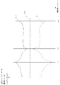
- the change in the voltage of the high frequency power when the voltage of the high frequency power supplied to the ultrasonic vibrator is changed so that the current detected by the current sensor becomes constant. It is a figure which shows the change of a current.
- FIG. 2 It is a flowchart which shows the operation of the ultrasonic vibration type defect detection apparatus shown in FIG. It is an enlarged plan view of the part A of FIG. 2 and the enlarged plan view of the part B shown in FIG. 6 when the substrate is ultrasonically vibrated.
- the change of the voltage of the high frequency power with respect to the frequency of the high frequency power is defined in advance so that the current of the high frequency power supplied to the ultrasonic vibrator is within a predetermined range. It is a figure which shows the other map. It is a system diagram which shows the structure of the wire defect detection system of embodiment. It is a flowchart which shows the operation of the wire defect detection system shown in FIG. It is a top view which shows the excess area when the substrate is ultrasonically vibrated.
- the ultrasonic vibration type defect detection device 100 of the embodiment will be described with reference to the drawings.
- the ultrasonic vibration type defect detection device 100 will be described as detecting defects in the wire 30 of the semiconductor device 10 which is an inspection target, but it is also used for detecting defects in other inspection objects. be able to.
- the ultrasonic vibration type defect detection device 100 includes an ultrasonic vibrator 42 which is an ultrasonic vibration device, a high frequency power supply 40, a camera 45 which is an image pickup device, and a control unit 50. It is configured.
- the semiconductor device 10 to be inspected by the ultrasonic vibration type defect detection device 100 has semiconductor chips 21 to 24 laminated and mounted in four stages on a substrate 11, and each semiconductor chip 21 is mounted.
- the electrodes 25 to 28 of No. 24 and the electrodes 12 of the substrate 11 are continuously connected by one wire 30.
- the semiconductor chips 21 to 24 constitute the semiconductor element 20.
- One wire 30 includes a first-stage wire 31 connecting the electrode 25 of the first-stage semiconductor chip 21 and the electrode 12 of the substrate 11, and electrodes 26 to each of the second-stage to fourth-stage semiconductor chips 22 to 24. It is composed of second-stage to fourth-stage wires 32 to 34 connecting 28 and electrodes 25 to 27 of each of the first-stage to third-stage semiconductor chips 21 to 23, respectively.
- the substrate 11 of the semiconductor device 10 and the semiconductor chips 21 to 24 form a non-target portion that is not a target of defect detection, and the wire 30 constitutes a target portion that detects defects.
- the high frequency power supply 40 outputs AC power having a frequency in the ultrasonic region and causes the ultrasonic vibrator 42 to be ultrasonically vibrated.
- the ultrasonic vibrator 42 is a member that is driven by high-frequency power in the frequency region of ultrasonic waves input from the high-frequency power supply 40 and vibrates ultrasonically. For example, it may be composed of a piezo element or the like.
- the ultrasonic vibrator 42 is connected to the substrate 11 of the semiconductor device 10 and causes the substrate 11 to be ultrasonically vibrated.
- a voltage sensor 53 that detects the voltage of the high-frequency power supplied from the high-frequency power supply 40 to the ultrasonic vibrator 42 and a current sensor 54 that detects the current of the high-frequency power. And are attached.
- the camera 45 is arranged on the upper side of the semiconductor device 10, and as shown in FIG. 2, the substrate 11 and the semiconductor chips 21 to 24 attached to the substrate 11 and the electrodes arranged on the outer peripheral portions of the semiconductor chips 21 to 24 are arranged. Images are taken of 25 to 28, the electrodes 12 of the substrate 11 arranged around the first-stage semiconductor chip 21, and the wires 30 for continuously connecting the electrodes 12 and 25 to 28.
- the control unit 50 is a computer including a CPU 51 and a memory 52 inside.
- the high frequency power supply 40 is connected to the control unit 50 and operates according to the command of the control unit 50.
- the camera 45 is connected to the control unit 50 and operates according to a command from the control unit 50.
- the moving image captured by the camera 45 is input to the control unit 50.
- the voltage sensor 53 and the current sensor 54 are connected to the control unit 50, and the voltage and current data of the high frequency power detected by the voltage sensor 53 and the current sensor 54 are input to the control unit 50.
- the control unit 50 captures an image of the semiconductor device 10 captured by the camera 45 while changing the frequency of the high frequency power supplied from the high frequency power supply 40 to the ultrasonic transducer 42, and the control unit 50 captures the image of the semiconductor device 10 based on the captured image. Inspect for defects.
- the ultrasonic vibrator 42 When the voltage V0 of the high frequency power supplied from the high frequency power supply 40 to the ultrasonic vibrator 42 is kept constant and the frequency f of the high frequency power is changed as in the one-point chain wire c0 shown in FIG. 3, the ultrasonic vibrator 42 itself. Resonates at frequency f1. As a result, the impedance of the ultrasonic transducer 42 greatly decreases at the frequency f1 as shown by the broken line a in FIG. On the other hand, at the frequency f2 between the frequency f1 and the maximum frequency f3, the impedance of the ultrasonic transducer 42 greatly increases.
- the high frequency power supplied to the ultrasonic transducer 42 is as shown by the solid line b0 in FIG.
- the current A0 rises significantly.
- the impedance of the ultrasonic vibrator 42 greatly increases in the vicinity of the frequency f2
- the current A0 of the high frequency power supplied to the ultrasonic vibrator 42 greatly decreases.
- the magnitude of the current A0 supplied to the ultrasonic vibrator 42 is proportional to the amplitude of the ultrasonic vibrator 42.
- the amplitude of the ultrasonic vibrator 42 greatly increases and the amplitude of the substrate 11 greatly increases, and in the vicinity of the frequency f2, the amplitude of the ultrasonic vibrator 42 increases. Is greatly reduced, and the amplitude of the substrate 11 is greatly reduced.
- the substrate 11, the semiconductor chips 21 to 24, and the wire 30 all vibrate significantly, so that the amplitude of the wire 30 is the substrate 11, the semiconductor chip 21 to It may be difficult to detect because it is hidden by the amplitude of 24.
- the amplitudes of the substrate 11, the semiconductor chips 21 to 24, and the wire 30 become very small, and the amplitude of the wire 30 may not be detected.
- the frequency near the resonance frequency f1 of the ultrasonic vibrator 42 is changed. In some cases, it may be difficult to detect the amplitude of the wire 30.
- the amplitude of the ultrasonic vibrator 42 is proportional to the current of the high frequency power input to the ultrasonic vibration device, and the ultrasonic vibrator 42
- the high frequency power current A1 input to is detected by the current sensor 54, and the high frequency power voltage V1 is adjusted so that the detected current A1 is within a predetermined range.
- the amplitude of the ultrasonic vibrator 42 can be set within a predetermined range while the high frequency power current A1 is within a predetermined range.
- the semiconductor device 10 is ultrasonically vibrated by changing the frequency of the high frequency power, the amplitude of the substrate 11 or the semiconductor element 20 which is the non-target portion of detection vibrates greatly at a specific frequency, and the target portion of detection. It is possible to prevent the amplitude of the wire 30 from being hidden by the amplitude of the substrate 11 and the semiconductor element 20 and becoming undetectable.
- the change operation of the voltage V1 of the high frequency power and the change operation of the current A1 when the above is changed will be described.
- the current A1 detected by the current sensor 54 is fed back to the control unit 50, and in the vicinity of the frequency f1 where the high frequency power current A1 increases, the one-point chain line c1 in FIG. As shown by, the voltage V1 of the high frequency power supplied to the ultrasonic transducer 42 is reduced. On the other hand, in the vicinity of the frequency f2 where the current A1 detected by the current sensor 54 decreases, the voltage V1 of the high frequency power supplied to the ultrasonic transducer 42 is increased as shown by the alternate long and short dash line c1 in FIG. As a result, as shown by the solid line d1 in FIG. 4, the magnitude of the current A1 detected by the current sensor 54 can be made substantially constant regardless of the frequency f.
- the voltage is set so that the ratio of the amplitude of the wire 30 detected from the image captured by the camera 45 to the amplitude of the substrate 11 detected from the image captured by the camera 45 and the semiconductor element 20 becomes equal to or higher than a predetermined value. You should adjust it. As a result, it is possible to suppress that the amplitude of the wire 30 is mixed with the amplitude of the substrate 11 or the semiconductor element 20 at each frequency f and the detection accuracy is lowered, and the amplitude of the wire 30 can be reliably detected, and the wire can be detected with high accuracy. 30 defects can be detected.
- the wire 30 is vibrated due to overvibration during defect detection. It can prevent damage.
- the CPU 51 of the control unit 50 changes the frequency f of the high frequency power while adjusting the voltage V1 of the high frequency power so that the current A1 detected by the current sensor 54 becomes substantially constant. While doing so, the semiconductor device 10 is ultrasonically vibrated.
- the control unit 50 captures a moving image of the vibrating semiconductor device 10 as shown in step S102 of FIG. 5, and stores the captured image data as shown in step S103 of FIG. 5 in the memory 52.
- the CPU 51 of the control unit 50 changes the frequency of the high-frequency power within the frequency range of a predetermined ultrasonic wave, captures a moving image of the semiconductor device 10 and stores it in the memory 52, and then proceeds to step S104 of FIG.
- the image of the wire 30 between the frame and the previous frame is compared, and the position difference ⁇ d is calculated.
- the wire 30a shown in detail in Part A of FIG. 6 is normally connected to each of the electrodes 12, 25 to 28.
- the first-stage to fourth-stage wires 31a to 34a are connected to the electrodes 12, 25 to 27 to which the lower ends of the first-stage to fourth-stage wires 31a to 34a are connected, respectively. It vibrates laterally at a natural frequency g0 between each of the electrodes 25 to 28 to which the upper end is connected.
- the natural frequency g0 differs depending on the diameter of the wire 30 and the distance L between the electrodes 25 and 26 and the electrodes 26 and 27, but in a general semiconductor device 10, it is often on the order of several tens of Hz.
- the defective wire 30b is in a non-attached state with the electrode 26 of the second-stage semiconductor chip 22. Therefore, when the defective wire 30b is ultrasonically vibrated, the second-stage wire 32b and the third-stage wire 33b are the electrodes 27 of the first-stage semiconductor chip 21 electrode 25 and the third-stage semiconductor chip 23. It vibrates laterally at the natural frequency g1 between and.
- the distance L between the electrodes 25 and the electrodes 27 is 2L, which is twice the distance L between the electrodes 25, 26 and the electrodes 26, 27, which is defective.
- the natural frequency g1 of the second-stage wire 32b and the third-stage wire 33b of the wire 30b is about 1 ⁇ 2 of g0, and is often on the order of 20 to 30 Hz in a general semiconductor device 10.
- the normally connected first-stage to fourth-stage wires 31a to 34a of the wires 30a vibrate laterally at a natural frequency g0 of several tens of Hz.
- the frame rate of the moving image is 24 to 60 frames per second. Therefore, for example, the images of the first-stage to fourth-stage wires 31a to 34a of one frame look like the alternate long and short dash line on the left side of the center line 39a of the wire 30a in the details of part A in FIG.
- the image of the front frame looks like the alternate long and short dash line on the right side of the center line 39a of the wire 30a in the details of part A in FIG.
- step S104 of FIG. 5 the PCU 51 of the control unit 50 has an image of the first to fourth stage wires 31a to 34a of one frame shown in detail of the A part of FIG.
- the difference ⁇ da between the images of the step wires 31a to 34a is calculated by comparing them with the images. As shown in detail in Part A of FIG. 6, this difference ⁇ da is small in the normal wire 30a.
- the difference ⁇ da is an amount proportional to the amplitude of the first-stage to fourth-stage wires 31a to 34a.
- the second-stage wire 32b and the third-stage wire 33b of the defective wire 30b which are not attached to the electrode 26 of the second-stage semiconductor chip 22, vibrate significantly in the lateral direction at 20 to 30 Hz. ..
- the frame rate of the moving image is 24 to 60 frames per second, for example, the images of the second-stage wire 32b and the third-stage wire 33b of one frame are shown in Part A of FIG.
- the details and the details of the B part are like the alternate long and short dash line on the left side of the center line 39b of the defective wire 30b. It looks like the alternate long and short dash line on the right side of 39b.
- the CPU 51 of the control unit 50 has an image of the second-stage wire 32b and the third-stage wire 33b of one frame and the previous front frame as shown in the details of the B portion of FIG.
- the difference ⁇ db between the image of the second-stage wire 32b and the image of the third-stage wire 33b is calculated.
- the difference ⁇ db between the second-stage wire 32b and the third-stage wire 33b of the defective wire 30b is very large and exceeds a predetermined threshold value ⁇ S.
- the difference ⁇ db is an amount proportional to the amplitude of the second-stage wire 32b and the third-stage wire 33b.
- the CPU 51 of the control unit 50 has an image of the second-stage wire 32b and the third-stage wire 33b of one frame, and the second-stage wire 32b and three of the previous previous frame.
- a predetermined threshold value ⁇ S it is determined as YES in step S105 of FIG. 5, and the process proceeds to step S106 of FIG.
- a wire defect detection signal indicating that the wire is defective is output to the outside.
- the CPU 51 of the control unit 50 determines NO in step S105 of FIG. 5 and proceeds to step S107 of FIG.
- the wire 30 of the device 10 outputs a wire good signal indicating that it is good to the outside.
- the ultrasonic vibration type defect detection device 100 of the embodiment controls the high frequency power by feeding back and controlling the current A1 of the high frequency power supplied from the high frequency power supply 40 to the ultrasonic vibrator 42 substantially constantly. Even when the frequency f of the above is changed, the amplitude of the ultrasonic vibrator 42 can be made substantially constant, and the amplitude of the substrate 11 and the semiconductor element 20 can be made substantially constant. Further, the voltage is adjusted so that the ratio of the amplitude of the wire 30 detected from the image captured by the camera 45 to the amplitude of the substrate 11 and the semiconductor element 20 detected from the image captured by the camera 45 becomes a predetermined value or more.
- the frequency at which the wire 30 vibrates greatly due to the non-attachment of the wire 30 varies variously depending on the position of the non-attachment, the distance L between the electrodes 12, 25 to 28, the diameter of the wire 30, and the like. Since the ultrasonic vibration type defect detection device 100 of the embodiment can reliably detect the amplitude of the wire 30 at various frequencies, the amplitude of the wire 30 can be detected at each frequency at which the amplitude of the wire 30 becomes large due to non-adhesion, and is high. Defect detection of the wire 30 can be performed with high accuracy in a short time.
- the frequency f of the high frequency power is changed by feedback control so that the current A1 of the high frequency power supplied from the high frequency power supply 40 to the ultrasonic vibrator 42 is substantially constant, the ultrasonic wave is generated.
- the amplitude of the oscillator 42 is substantially constant, the present invention is not limited to this.
- the change in the high frequency power current A0 when the frequency is changed with the high frequency power voltage V0 constant by a test or the like is acquired, and the one-point chain line c2 is shown in FIG.
- a voltage waveform in which the increase and decrease of the current A0 are reversed is generated, and this voltage waveform is stored in the memory 52 as a map 55 showing the change of the voltage V2 with respect to the frequency f.
- the map 55 has a waveform in which the voltage becomes low in the vicinity of the frequency f1 and the voltage becomes high in the frequency f2.
- the voltage with respect to the frequency f may be adjusted with reference to the map 55 stored in the memory 52. Also in this case, as shown by the solid line d2 in FIG. 7, the current A2 supplied to the ultrasonic transducer 42 is substantially constant even if the frequency changes.
- the semiconductor device 10 when the semiconductor device 10 is ultrasonically vibrated in various frequency bands with a simple configuration, the entire semiconductor device 10 vibrates greatly, and the amplitude of the wire 30 which is the target portion is the amplitude of the substrate 11 or the semiconductor element 20. It is possible to suppress the fact that it cannot be detected because it is hidden behind the surface, and it is possible to detect defects in the target portion of the inspection target with high accuracy.
- a voltage waveform that changes the voltage V3 stepwise with respect to the frequency f is stored in the memory 52 as a map 56. May be good.
- the current A3 supplied to the ultrasonic transducer 42 is not substantially constant, but falls within a predetermined range ⁇ A. As a result, it is possible to detect the defect of the wire 30 with high accuracy and in a short time by a simpler method.
- the CPU 51 of the control unit 50 ultrasonically vibrates the semiconductor device 10, the number of frames between one frame for calculating the difference ⁇ d of the image of the wire 30 and the previous frame, or the frame rate of the moving image. May be changed to calculate the difference ⁇ d of the image of the wire 30. As a result, even when the frequency of the wire 30 changes, the difference ⁇ d of the image of the wire 30 can be detected, and the defect detection accuracy can be improved.
- the wire defect detection system 200 shown in FIG. 9 includes a substrate 11, semiconductor chips 21 to 24 attached to the substrate 11, electrodes 25 to 28 of the semiconductor chips 21 to 24, electrodes 12 of the substrate 11, or a semiconductor chip 21. Detects a defect in the wire 30 of the semiconductor device 10 including the wires 31 to 34 connecting the electrodes 25 to 28 of 1 to 24 and the other electrodes 25 to 28 of the semiconductor chips 21 to 24.
- the ultrasonic vibrator 42 which is the ultrasonic vibrator of the ultrasonic vibration type defect detection device 100 described above, is used as the ultrasonic speaker 43, and the image captured by the camera 45 on the control unit 50.
- a display 48 for displaying the above is added. Further, the wire defect detection system 200 does not include the voltage sensor 53 and the current sensor 54 attached to the ultrasonic vibration type defect detection device 100, and refers to FIGS. 7 and 8 in the memory 52 of the control unit 50.
- the map 55 or the map 56 described above is stored. Then, when the frequency f of the high frequency power supplied from the high frequency power supply 40 to the ultrasonic speaker 43 is changed, the CPU 51 of the control unit 50 supplies the high frequency power supply 40 to the ultrasonic speaker 43 based on the map 55 or the map 56. Adjust the voltage of the high frequency power to be done.
- the configuration other than the above is the same as that of the ultrasonic vibration type defect detection device 100 described above.
- the ultrasonic speaker 43 is arranged around the semiconductor device 10 and ultrasonically vibrates the semiconductor device 10.
- the CPU 51 of the control unit 50 adjusts the high frequency power voltage V1 so that the current A1 detected by the current sensor 54 is substantially constant, and the frequency of the high frequency power.
- the semiconductor device 10 is ultrasonically vibrated while changing f. Then, the CPU 51 of the control unit 50 captures a moving image of the wire 30 of the vibrating semiconductor device 10, and stores the captured image data in the memory 52.
- control unit 50 changes the frequency of the high-frequency power within the frequency range of a predetermined ultrasonic wave, captures a moving image of the semiconductor device 10 and stores it in the memory 52, and then, as described above, one The images of the frame and the previous frame are compared, and the difference ⁇ d of the images of the wire 30 is calculated.
- the CPU 51 of the control unit 50 has an image of the second-stage wire 32b and the third-stage wire 33b of one frame, and the second-stage wire 32b and three of the previous previous frame.
- a predetermined threshold value ⁇ S it is determined as YES in step S105 of FIG. 10, and the process proceeds to step S202 of FIG.
- the display image on the display 48 of the image is different from the display image of the first-stage to fourth-stage wires 31a to 34a of the normally connected wire 30a.
- the images of the second stage wire 32b and the third stage wire 33b of the defective wire 30b may be displayed in red. Further, it is displayed in white with high brightness so that it can be distinguished from the image of the substrate 11 and each semiconductor chip 21 to 24, or the image of the first to fourth stage wires 31a to 34a of the normally connected wire 30a. It may be displayed.
- the defective wire 30b is displayed in red, so that the presence or absence of the defective wire 30b and its position can be detected at a glance.
- step S105 of FIG. 10 the CPU 51 ends the process without disagreeing the images.
- the CPU 51 of the control unit 50 has an image of the second-stage wire 32b and the third-stage wire 33b of one frame, and the second-stage wire 32b and the third-stage wire of the previous previous frame.
- the difference ⁇ db of the wire 33b from the image exceeds a predetermined threshold value ⁇ S
- the difference ⁇ db in the vibration region of the second stage wire 32b and the third stage wire 33b shown by hatching in FIG. 11 sets the predetermined threshold value ⁇ S.
- the image display of the exceeded excess areas 35 and 36 may be displayed on the display 48 differently from the image display of the other areas.
- the area wider than the images of the second-stage wire 32b and the third-stage wire 33b of the defective wire 30b is displayed in red, so that the inspector can more easily display the defect.
- the wire 30b can be detected.
- the wire defect detection system 200 of the embodiment has the same effect as the ultrasonic vibration type defect detection device 100 described above, and another display image of the defective wire 30b is displayed on the display 48. It can be displayed separately from the displayed image. This allows the inspector to detect the defective wire 30b from the image on the display 48. Since the difference between the amplitude of the defective wire 30b and the amplitude of the normally connected wire 30a is remarkable, it is possible to detect the defect of the defective wire 30b with high accuracy. Further, since the camera 45 can acquire images of all the wires 30 included in the semiconductor device 10 and simultaneously analyze them and display them on the display 48, all the wires 30 can be obtained in a short time even if the number of wires 30 increases. Can be inspected for defects.
Landscapes
- Physics & Mathematics (AREA)
- Biochemistry (AREA)
- General Physics & Mathematics (AREA)
- Pathology (AREA)
- Health & Medical Sciences (AREA)
- Life Sciences & Earth Sciences (AREA)
- Chemical & Material Sciences (AREA)
- Immunology (AREA)
- Analytical Chemistry (AREA)
- General Health & Medical Sciences (AREA)
- Engineering & Computer Science (AREA)
- Mechanical Engineering (AREA)
- Signal Processing (AREA)
- Computer Vision & Pattern Recognition (AREA)
- Optics & Photonics (AREA)
- Acoustics & Sound (AREA)
- Investigating Or Analyzing Materials By The Use Of Ultrasonic Waves (AREA)
Priority Applications (5)
| Application Number | Priority Date | Filing Date | Title |
|---|---|---|---|
| US18/015,074 US12438053B2 (en) | 2020-10-28 | 2020-10-28 | Ultrasound vibrating-type defect detection apparatus and wire defect detection system |
| CN202080102531.5A CN115769350A (zh) | 2020-10-28 | 2020-10-28 | 超声波振动式不良检测装置及线材不良检测系统 |
| JP2022558668A JP7432263B2 (ja) | 2020-10-28 | 2020-10-28 | 超音波加振式不良検出装置及びワイヤ不良検出システム |
| PCT/JP2020/040416 WO2022091247A1 (ja) | 2020-10-28 | 2020-10-28 | 超音波加振式不良検出装置及びワイヤ不良検出システム |
| KR1020237008003A KR102741806B1 (ko) | 2020-10-28 | 2020-10-28 | 초음파 가진식 불량 검출 장치 및 와이어 불량 검출 시스템 |
Applications Claiming Priority (1)
| Application Number | Priority Date | Filing Date | Title |
|---|---|---|---|
| PCT/JP2020/040416 WO2022091247A1 (ja) | 2020-10-28 | 2020-10-28 | 超音波加振式不良検出装置及びワイヤ不良検出システム |
Publications (1)
| Publication Number | Publication Date |
|---|---|
| WO2022091247A1 true WO2022091247A1 (ja) | 2022-05-05 |
Family
ID=81382027
Family Applications (1)
| Application Number | Title | Priority Date | Filing Date |
|---|---|---|---|
| PCT/JP2020/040416 Ceased WO2022091247A1 (ja) | 2020-10-28 | 2020-10-28 | 超音波加振式不良検出装置及びワイヤ不良検出システム |
Country Status (5)
| Country | Link |
|---|---|
| US (1) | US12438053B2 (https=) |
| JP (1) | JP7432263B2 (https=) |
| KR (1) | KR102741806B1 (https=) |
| CN (1) | CN115769350A (https=) |
| WO (1) | WO2022091247A1 (https=) |
Families Citing this family (1)
| Publication number | Priority date | Publication date | Assignee | Title |
|---|---|---|---|---|
| CN118379238B (zh) * | 2024-03-19 | 2025-01-14 | 湖南隆深氢能科技有限公司 | 基于原纸石墨化设备的瑕疵检测方法、系统、终端及介质 |
Citations (8)
| Publication number | Priority date | Publication date | Assignee | Title |
|---|---|---|---|---|
| JPH09182467A (ja) * | 1995-12-27 | 1997-07-11 | Nikon Corp | 振動アクチュエータの駆動装置 |
| JP2007203199A (ja) * | 2006-02-02 | 2007-08-16 | Kaijo Corp | 超音波振動子の駆動装置 |
| JP2008084881A (ja) * | 2006-09-25 | 2008-04-10 | Toshiba Corp | 電子装置の製造方法およびその検査方法 |
| WO2011036751A1 (ja) * | 2009-09-24 | 2011-03-31 | 株式会社 東芝 | 電子機器および損傷検出方法 |
| JP2012083246A (ja) * | 2010-10-13 | 2012-04-26 | Toyota Motor Corp | 接合検査方法 |
| JP2014024065A (ja) * | 2012-07-24 | 2014-02-06 | Adwelds:Kk | 異常検出装置および異常検出方法 |
| JP2016024186A (ja) * | 2014-07-17 | 2016-02-08 | ザ・ボーイング・カンパニーTheBoeing Company | ハイパーサウンドを使用した非破壊検査 |
| JP2020134289A (ja) * | 2019-02-19 | 2020-08-31 | キオクシア株式会社 | 半導体装置の検査方法及び検査装置 |
Family Cites Families (3)
| Publication number | Priority date | Publication date | Assignee | Title |
|---|---|---|---|---|
| JPH09213752A (ja) | 1996-01-31 | 1997-08-15 | Kaijo Corp | ワイヤボンディング装置における不着検出回路 |
| CA2496935C (en) * | 2002-08-28 | 2011-09-13 | Wayne State University | System and method for acoustic chaos in sonic infrared imaging |
| JP2010056106A (ja) | 2008-08-26 | 2010-03-11 | Nec Electronics Corp | ワイヤボンディング装置、これを用いたワイヤボンディング方法 |
-
2020
- 2020-10-28 CN CN202080102531.5A patent/CN115769350A/zh active Pending
- 2020-10-28 US US18/015,074 patent/US12438053B2/en active Active
- 2020-10-28 WO PCT/JP2020/040416 patent/WO2022091247A1/ja not_active Ceased
- 2020-10-28 JP JP2022558668A patent/JP7432263B2/ja active Active
- 2020-10-28 KR KR1020237008003A patent/KR102741806B1/ko active Active
Patent Citations (8)
| Publication number | Priority date | Publication date | Assignee | Title |
|---|---|---|---|---|
| JPH09182467A (ja) * | 1995-12-27 | 1997-07-11 | Nikon Corp | 振動アクチュエータの駆動装置 |
| JP2007203199A (ja) * | 2006-02-02 | 2007-08-16 | Kaijo Corp | 超音波振動子の駆動装置 |
| JP2008084881A (ja) * | 2006-09-25 | 2008-04-10 | Toshiba Corp | 電子装置の製造方法およびその検査方法 |
| WO2011036751A1 (ja) * | 2009-09-24 | 2011-03-31 | 株式会社 東芝 | 電子機器および損傷検出方法 |
| JP2012083246A (ja) * | 2010-10-13 | 2012-04-26 | Toyota Motor Corp | 接合検査方法 |
| JP2014024065A (ja) * | 2012-07-24 | 2014-02-06 | Adwelds:Kk | 異常検出装置および異常検出方法 |
| JP2016024186A (ja) * | 2014-07-17 | 2016-02-08 | ザ・ボーイング・カンパニーTheBoeing Company | ハイパーサウンドを使用した非破壊検査 |
| JP2020134289A (ja) * | 2019-02-19 | 2020-08-31 | キオクシア株式会社 | 半導体装置の検査方法及び検査装置 |
Also Published As
| Publication number | Publication date |
|---|---|
| US12438053B2 (en) | 2025-10-07 |
| KR20230054686A (ko) | 2023-04-25 |
| JPWO2022091247A1 (https=) | 2022-05-05 |
| JP7432263B2 (ja) | 2024-02-16 |
| CN115769350A (zh) | 2023-03-07 |
| KR102741806B1 (ko) | 2024-12-11 |
| US20230253266A1 (en) | 2023-08-10 |
Similar Documents
| Publication | Publication Date | Title |
|---|---|---|
| JP6089499B2 (ja) | 超音波トランスデューサー装置およびプローブ並びに電子機器および超音波診断装置 | |
| US20110155789A1 (en) | Bonding apparatus | |
| US12487206B2 (en) | Defect detection device and defect detection method | |
| US20140360272A1 (en) | Capacitive transducer drive device and object information acquiring device | |
| KR100820380B1 (ko) | 초음파 프로브에 사용되는 압전 소자를 재분극하는 재분극시스템 | |
| TWI823376B (zh) | 不良檢測裝置及不良檢測方法 | |
| WO2022091247A1 (ja) | 超音波加振式不良検出装置及びワイヤ不良検出システム | |
| HK1040951A1 (zh) | 测量焊接参数用的压电传感器 | |
| JP7019231B2 (ja) | ワイヤ不着検査システム及びワイヤ不着検出装置並びにワイヤ不着検出方法 | |
| JP2010041638A (ja) | マイクロホン装置の検査装置 | |
| JP2012083246A (ja) | 接合検査方法 | |
| TWI802991B (zh) | 超音波振動式不良檢測裝置及線材不良檢測系統 | |
| US20080223136A1 (en) | Minute structure inspection device, inspection method, and inspection program | |
| JP7308577B2 (ja) | 音響式不良検出装置及び不良検出方法 | |
| JPWO2022091247A5 (https=) | ||
| JP2007189113A (ja) | プローブ触針検知法及び装置 | |
| CN103284756B (zh) | 探头单元、超声波探测器、电子设备及诊断装置 | |
| TWI334031B (en) | Testing system and testing method for display apparatus | |
| WO2018012214A1 (ja) | 半導体センサチップ、半導体センサチップアレイ、および超音波診断装置 | |
| JP2013187374A (ja) | 半導体後工程組立装置 |
Legal Events
| Date | Code | Title | Description |
|---|---|---|---|
| 121 | Ep: the epo has been informed by wipo that ep was designated in this application |
Ref document number: 20959765 Country of ref document: EP Kind code of ref document: A1 |
|
| ENP | Entry into the national phase |
Ref document number: 2022558668 Country of ref document: JP Kind code of ref document: A |
|
| ENP | Entry into the national phase |
Ref document number: 20237008003 Country of ref document: KR Kind code of ref document: A |
|
| NENP | Non-entry into the national phase |
Ref country code: DE |
|
| 122 | Ep: pct application non-entry in european phase |
Ref document number: 20959765 Country of ref document: EP Kind code of ref document: A1 |
|
| WWG | Wipo information: grant in national office |
Ref document number: 18015074 Country of ref document: US |
|
| WWG | Wipo information: grant in national office |
Ref document number: 11202300185R Country of ref document: SG |
|
| WWP | Wipo information: published in national office |
Ref document number: 11202300185R Country of ref document: SG |