WO2022085164A1 - 電波吸収体 - Google Patents
電波吸収体 Download PDFInfo
- Publication number
- WO2022085164A1 WO2022085164A1 PCT/JP2020/039768 JP2020039768W WO2022085164A1 WO 2022085164 A1 WO2022085164 A1 WO 2022085164A1 JP 2020039768 W JP2020039768 W JP 2020039768W WO 2022085164 A1 WO2022085164 A1 WO 2022085164A1
- Authority
- WO
- WIPO (PCT)
- Prior art keywords
- radio wave
- conductor pattern
- antenna element
- modification
- conductor
- Prior art date
- Legal status (The legal status is an assumption and is not a legal conclusion. Google has not performed a legal analysis and makes no representation as to the accuracy of the status listed.)
- Ceased
Links
Images


Classifications
-
- H—ELECTRICITY
- H05—ELECTRIC TECHNIQUES NOT OTHERWISE PROVIDED FOR
- H05K—PRINTED CIRCUITS; CASINGS OR CONSTRUCTIONAL DETAILS OF ELECTRIC APPARATUS; MANUFACTURE OF ASSEMBLAGES OF ELECTRICAL COMPONENTS
- H05K9/00—Screening of apparatus or components against electric or magnetic fields
Definitions
- the present invention relates to a radio wave absorber.
- Japanese Unexamined Patent Publication No. 2007-0736662 Japanese Unexamined Patent Publication No. 2005-317945 Japanese Unexamined Patent Publication No. 2009-071278
- the radio wave absorber described in the above patent document can absorb a wide band radio wave, but when it is made thinner, it becomes a narrow band. Therefore, there is a problem in the radio wave absorption efficiency in the usage such as using the radio wave absorber as the wallpaper of the room or providing the radio wave absorber on the seat surface of the seat.
- One aspect of the disclosed technique is to provide a radio wave absorber capable of further improving the radio wave absorption efficiency.
- This radio wave absorber has a dielectric layer formed in a sheet shape, a conductor layer formed on one surface of the dielectric layer, and a plurality of conductor patterns arranged on the other surface of the dielectric layer. Be prepared. Each of the plurality of conductor patterns is formed in a frame shape and resonates with a radio wave of the first wavelength, and is formed in a plate shape and inscribed in the frame shape element, and has a second wavelength shorter than the first wavelength. Includes plate-shaped elements that resonate with radio waves.
- a part of the frame-shaped element that resonates with the radio wave of the first wavelength is shared as a part of the plate-shaped element that resonates with the radio wave of the second wavelength shorter than the first wavelength, thereby absorbing the radio wave. It is possible to provide a radio wave absorber capable of increasing efficiency.
- FIG. 1 is a first diagram showing an example of a radio wave absorption sheet according to an embodiment.
- FIG. 2 is a second diagram showing an example of the radio wave absorption sheet according to the embodiment.
- FIG. 3 is a third diagram showing an example of the radio wave absorption sheet according to the embodiment.
- FIG. 4 is a diagram illustrating the shape of the conductor pattern in the embodiment.
- FIG. 5 is a perspective view illustrating the size set in the simulation for the radio wave absorbing sheet according to the embodiment.
- FIG. 6 is a first diagram illustrating the simulation result of the radio wave absorption sheet according to the embodiment.
- FIG. 7 is a second diagram illustrating the simulation result of the radio wave absorption sheet according to the embodiment.
- FIG. 1 is a first diagram showing an example of a radio wave absorption sheet according to an embodiment.
- FIG. 2 is a second diagram showing an example of the radio wave absorption sheet according to the embodiment.
- FIG. 3 is a third diagram showing an example of the radio wave absorption sheet according to the
- FIG. 8 is a first diagram showing an example of a radio wave absorption sheet according to the first comparative example.
- FIG. 9 is a second diagram showing an example of the radio wave absorption sheet according to the first comparative example.
- FIG. 10 is a diagram illustrating a simulation result of the radio wave absorption sheet according to the first comparative example.
- FIG. 11 is a first diagram showing an example of a radio wave absorbing sheet according to a second comparative example.
- FIG. 12 is a second diagram showing an example of the radio wave absorption sheet according to the second comparative example.
- FIG. 13 is a diagram showing a simulation result of the radio wave absorption sheet according to the second comparative example.
- FIG. 14 is a first diagram showing an example of a radio wave absorption sheet according to a third comparative example.
- FIG. 14 is a first diagram showing an example of a radio wave absorption sheet according to a third comparative example.
- FIG. 15 is a second diagram showing an example of the radio wave absorption sheet according to the third comparative example.
- FIG. 16 is a first diagram illustrating the simulation result of the radio wave absorption sheet according to the third comparative example.
- FIG. 17 is a second diagram illustrating the simulation result of the radio wave absorption sheet according to the third comparative example.
- FIG. 18 is a first diagram illustrating a simulation result in which the width of the loop slot is varied in the third comparative example.
- FIG. 19 is a second diagram illustrating a simulation result in which the width of the loop slot is varied in the third comparative example.
- FIG. 20 is a schematic diagram illustrating the relationship between the line width of the loop antenna element and the resistance of the material of the conductor pattern in the third comparative example.
- FIG. 21 is a diagram showing an example of a conductor pattern in the first modification.
- FIG. 22 is a diagram showing an example of the conductor pattern in the second modification.
- FIG. 23 is a diagram illustrating the comparison results of the first modified example and the second modified example by simulation.
- FIG. 24 is a Smith chart illustrating the comparison results of the first modified example and the second modified example by simulation.
- FIG. 25 is a diagram showing an example of a conductor pattern in the third modification.
- FIG. 26 is a diagram showing an example of a conductor pattern in the fourth modification.
- FIG. 27 is a diagram illustrating the comparison results of the third modified example and the fourth modified example by simulation.
- FIG. 28 is a Smith chart illustrating the comparison results of the third modified example and the fourth modified example by simulation.
- FIG. 28 is a Smith chart illustrating the comparison results of the third modified example and the fourth modified example by simulation.
- FIG. 29 is a diagram illustrating the shape of the conductor pattern in the fifth modification.
- FIG. 30 is a diagram illustrating the shape of the conductor pattern in the fifth modification.
- FIG. 31 is a diagram illustrating the shape of the conductor pattern in the sixth modification.
- FIG. 32 is a diagram illustrating the shape of the conductor pattern in the seventh modification.
- FIG. 33 is a diagram illustrating the shape of the conductor pattern in the eighth modification.
- FIG. 34 is a diagram illustrating the shape of the conductor pattern in the ninth modification.
- FIG. 35 is a diagram illustrating a case where three patch antenna elements are provided in the conductor pattern in the ninth modification.
- FIG. 36 is a diagram illustrating the shape of the conductor pattern in the tenth modification.
- FIG. 37 is a diagram illustrating the shape of the conductor pattern in the eleventh modification.
- FIG. 38 is a diagram illustrating the shape of the conductor pattern in the twelfth modification.
- FIG. 39 is a first diagram illustrating the arrangement of the conductor pattern on the radio wave absorbing sheet.
- FIG. 40 is a second diagram illustrating the arrangement of the conductor pattern on the radio wave absorbing sheet.
- the radio wave absorber according to the embodiment is, for example, a dielectric layer formed in a sheet shape, a conductor layer formed on one surface of the dielectric layer, and a plurality of arranged on the other surface of the dielectric layer. With a conductor pattern.
- Each of the plurality of conductor patterns is formed in a frame shape and resonates with a radio wave of the first wavelength, and is formed in a plate shape and inscribed in the frame shape element, and has a second wavelength shorter than the first wavelength. Includes plate-shaped elements that resonate with radio waves.
- the radio wave of the first wavelength can be received by the frame-shaped element, and the radio wave of the second wavelength can be received by the plate-shaped element.
- the radio wave absorber can attenuate the received first radio wave and the second radio wave by the dielectric layer even if the dielectric layer is thinly formed.
- the radio wave absorber has a radio wave absorption efficiency by sharing a part of the frame-shaped element that resonates with the radio wave of the first wavelength as a part of the plate-shaped element that resonates with the radio wave of the second wavelength shorter than the first wavelength. Therefore, it is possible to realize a radio wave absorber that can be made thinner.
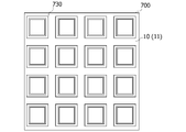
- FIG. 1 to 3 are views showing an example of a radio wave absorbing sheet according to an embodiment.
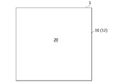
- FIG. 1 is a front view of the radio wave absorption sheet according to the embodiment.
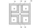
- FIG. 2 is an enlarged perspective view of a conductor pattern arranged on the radio wave absorbing sheet according to the embodiment.
- FIG. 3 is a rear view of the radio wave absorbing sheet according to the embodiment.
- the radio wave absorbing sheet 1 includes a dielectric layer 10, a conductor layer 20, and a plurality of conductor patterns 30, and the whole thereof is formed in a sheet shape.
- a plurality of conductor patterns 30 are arranged apart from each other on the front surface 11 of the dielectric layer 10 formed in a sheet shape.
- a conductor layer 20 is formed on the back surface 12 of the dielectric layer 10.
- the dielectric layer 10 is formed of an insulator.
- the insulator include rubber, plastic, resin, glass, paper, air and the like.
- the thickness T of the dielectric layer 10 is, for example, 5.0 mm.
- the conductor layer 20 is formed of a conductor such as metal. Examples of the conductor include copper, gold, aluminum and the like. As illustrated in FIG. 3, the conductor layer 20 is formed on the entire back surface 12 of the dielectric layer 10.
- the conductor pattern 30 is formed of a conductor such as metal, similarly to the conductor layer 20.
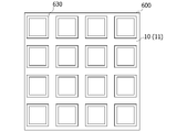
- a plurality of conductor patterns 30 are periodically arranged side by side on the front surface 11 of the dielectric layer 10.
- FIG. 4 is a diagram illustrating the shape of the conductor pattern in the embodiment.
- a loop antenna element 31 and four patch antenna elements 32 are formed by providing a cross-shaped hole 34 in a plate member formed of a conductor.
- the loop antenna element 31 and the patch antenna element 32 are each provided with diagonal lines having different inclination directions.
- a solid line is provided between the loop antenna element 31 and the patch antenna element 32 to help understanding, but the loop antenna element 31 and the patch antenna element 32 are not formed of different materials. not.
- the loop antenna element 31 and the patch antenna element 32 are, for example, integrally formed.
- the loop antenna element 31 and the patch antenna element 32 may be formed separately, and then the loop antenna element 31 and the patch antenna element 32 may be combined to form the conductor pattern 30.
- the loop antenna element 31 forms a rectangular frame of the conductor pattern 30.
- the loop antenna element 31 is designed to resonate with a radio wave having a frequency of 2.5 GHz among the two frequency bands (2.4 GHz band and 5.0 GHz band) used in the wireless Local Area Network (LAN).
- One side of the loop antenna element 31 formed in a rectangular shape is formed to have a length of 1/4 wavelength of a radio wave having a frequency of 2.5 GHz. That is, the length of the loop antenna element 31 has one wavelength of radio waves having a frequency of 2.5 GHz.
- the length of one side of the loop antenna element 31 does not have to exactly match the length of the 1/4 wavelength of the radio wave having a frequency of 2.5 GHz.
- the length of one side of the loop antenna element 31 may be appropriately adjusted so that the loop antenna element 31 resonates with a radio wave having a frequency of 2.5 GHz.
- the loop antenna element 31 is an example of a “frame-shaped element”.
- the patch antenna element 32 is a rectangular plate-shaped element inscribed in the loop antenna element 31. Each of the patch antenna elements 32 is arranged so as to be inscribed in different angles of the loop antenna element 31. Each of the patch antenna elements 32 is separated from each other by a cross-shaped hole 34.
- One side of the patch antenna element 32 formed in a rectangular shape has a length of 1/4 wavelength of the radio wave having a frequency of 5.0 GHz among the two frequency bands (2.4 GHz band and 5.0 GHz band) used in the wireless LAN. It is formed in the air. That is, the length of the outer circumference of the patch antenna element 32 31 has a length of one wavelength of a radio wave having a frequency of 5.0 GHz.
- the length of one side of the patch antenna element 32 does not have to exactly match the length of 1/4 wavelength of the radio wave having a frequency of 5.0 GHz.
- the length of one side of the patch antenna element 32 may be appropriately adjusted so that the patch antenna element 32 resonates with a radio wave having a frequency of 5.0 GHz.
- the patch antenna element 32 may be provided with a rectangular through hole 33 penetrating in the thickness direction of the patch antenna element 32.
- the distance D (see FIG. 1) of the plurality of conductor patterns 30 arranged is set to a distance at which the loop antenna elements 31 of the adjacent conductor patterns 30 are capacitively coupled. That is, in the radio wave absorbing sheet 1, it can be said that the unit structure including the conductor pattern 30 and the dielectric layer 10 exposed in the width of D / 2 is periodically arranged around the conductor pattern 30.
- the patch antenna element 32 is an example of a “plate-shaped element”.
- FIG. 5 is a perspective view illustrating the size set in the simulation for the radio wave absorbing sheet according to the embodiment.
- the length L of one side of the conductor pattern 30 is 35.20 mm
- the line width W1 of the loop antenna element 31 is 4.40 mm
- the line width W2 of the patch antenna element 32 is 4.40 mm
- the width L2 of the patch antenna element 32 is 15.
- the thickness T of the dielectric layer 10 was set to 13 mm and 10.00 mm.
- the height H of the periodic structure including the conductor pattern 30 and the exposed dielectric layer 10 was set to 44.00 mm.
- the conductivity of the conductor layer 20 and the conductor pattern 30 was set to 1e + 4 (S / m), and the relative permittivity of the dielectric layer 10 was set to 1.0.
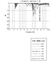
- FIG. 6 and 7 are diagrams illustrating simulation results of the radio wave absorption sheet according to the embodiment.
- FIG. 6 illustrates the radio wave absorption characteristics of the radio wave absorption sheet 1.
- the vertical axis represents absorption efficiency (dB) and the horizontal axis represents frequency (GHz).
- FIG. 7 illustrates a Smith chart of the radio wave absorption sheet 1. Assuming that the range where the absorption efficiency is -10db or less is the region where the desired performance is exhibited, the radio wave absorption sheet 1 can exhibit the desired radio wave absorption characteristics in the two frequency bands of 2.4 GHz and 5.0 GHz. Understandable.
- FIG. 8 and 9 are views showing an example of a radio wave absorbing sheet according to the first comparative example.
- FIG. 8 is a front view of the radio wave absorbing sheet according to the first comparative example.
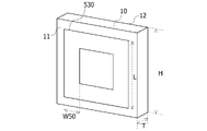
- FIG. 9 is a perspective view illustrating the shape of the conductor pattern according to the first comparative example.
- a plurality of conductor patterns 530 are arranged in place of the conductor pattern 30.
- the conductor pattern 530 is formed in the shape of a rectangular frame.
- the line width W50 (see FIG. 9) of the conductor pattern 530 was set to 9.50 mm.
- the conductivity of the conductor pattern 530, the length L of one side of the conductor pattern 530, the thickness T of the dielectric layer 10, and the height H of the periodic structure including the conductor pattern 530 and the exposed dielectric layer 10 are the embodiments. The value was the same as that of the radio wave absorbing sheet 1.
- FIG. 10 is a diagram illustrating the simulation result of the radio wave absorption sheet according to the first comparative example.
- FIG. 10 illustrates the radio wave absorption characteristics of the radio wave absorption sheet 500.
- the vertical axis represents absorption efficiency (dB) and the horizontal axis represents frequency (GHz).
- dB absorption efficiency
- GHz frequency
- the radio wave absorbing sheet 500 cannot exhibit the desired performance in any of the 2.4 GHz and 5.0 GHz frequency bands. I can understand that.
- FIG. 11 and 12 are views showing an example of a radio wave absorbing sheet according to the second comparative example.
- FIG. 11 is a front view of the radio wave absorption sheet according to the second comparative example.
- FIG. 12 is a perspective view illustrating the shape of the conductor pattern according to the second comparative example.
- a plurality of conductor patterns 630 are arranged in place of the conductor pattern 30.
- the conductor pattern 630 is formed in the shape of a rectangular frame.
- the line width W60 (see FIG. 12) of the conductor pattern 630 was set to 2.11 mm
- the thickness T60 of the dielectric layer 10 (see FIG. 12) was set to 15.00 mm.
- the conductivity of the conductor pattern 630, the length L of one side of the conductor pattern 630, and the height H of the periodic structure including the conductor pattern 630 and the exposed dielectric layer 10 have the same values as those of the radio wave absorbing sheet 1 according to the embodiment. bottom. That is, it can be said that the conductor pattern 630 according to the second comparative example has a line width W60 and a thickness T60 of the dielectric layer 10 changed from the conductor pattern 530 according to the first comparative example.
- FIG. 13 is a diagram showing a simulation result of the radio wave absorption sheet according to the second comparative example.
- the vertical axis represents absorption efficiency (dB) and the horizontal axis represents frequency (GHz).
- dB absorption efficiency
- GHz frequency
- the radio wave absorption sheet 600 exhibits the desired radio wave absorption characteristics in the two frequency bands of 2.4 GHz and 5.0 GHz. Can be understood.
- FIG. 14 and 15 are views showing an example of a radio wave absorbing sheet according to a third comparative example.
- FIG. 14 is a front view of the radio wave absorption sheet according to the third comparative example.
- FIG. 15 is a perspective view illustrating the shape of the conductor pattern according to the third comparative example.
- a plurality of conductor patterns 730 are arranged in place of the conductor pattern 30.
- the loop antenna element 731 and the patch antenna element 732 are formed by forming a rectangular loop slot 733 that penetrates a plate-shaped conductor (for example, copper) having a side of 18 mm in the thickness direction.
- the width of the loop slot 733 (distance between the loop antenna element 731 and the patch antenna element 732) was set to 1 mm.
- the central loop length of the loop slot 733 was set to 44 mm.
- a plurality of conductor patterns 730 are arranged so that the center spacing is 22 mm.
- 16 and 17 are diagrams illustrating simulation results of the radio wave absorption sheet according to the third comparative example. 16 and 17 show simulation results when the dielectric loss tangent (tan ⁇ ) of the dielectric layer 10 is changed in the range of 0.1 to 0.001.
- the vertical axis represents absorption efficiency (dB) and the horizontal axis represents frequency (GHz).
- dB absorption efficiency
- GHz frequency
- the radio wave absorbing sheet 700 cannot exhibit the performance of -10db or less in any of the frequency bands of 2.4 GHz and 5.0 GHz.
- the resistance of the conductor pattern 730 greatly fluctuates by changing the value of tan ⁇ .
- the line width of the loop antenna element 731 fluctuates from 3.0 mm to 0.05 mm as the width of the loop slot 733 is fluctuated. Therefore, in this simulation, it can be said that the line width of the loop antenna element 731 was changed from 3.0 mm to 0.05 mm.
- FIG. 18 and 19 are diagrams illustrating simulation results in which the width of the loop slot is varied in the third comparative example.
- the vertical axis represents absorption efficiency (dB) and the horizontal axis represents frequency (GHz).
- dB absorption efficiency
- GHz frequency
- the radio wave absorption sheet 700 can change the frequency band exhibiting high radio wave absorption characteristics by changing the line width of the loop antenna element 731.
- the resistance of the radio wave absorbing sheet 700 also fluctuates according to the fluctuation of the line width of the loop antenna element 731.
- FIG. 20 is a schematic diagram illustrating the relationship between the line width of the loop antenna element and the resistance of the material of the conductor pattern in the third comparative example.
- the vertical axis illustrates the line width of the loop antenna element 731
- the horizontal axis illustrates the resistance of the conductor pattern 730.
- the line width becomes narrower as it goes up.
- the resistance of the conductor pattern 730 decreases as it goes to the right.
- the line width of the loop antenna element 731 has an upper limit value and a lower limit value due to the influence of the formation of the loop slot 733 and the processing accuracy. Further, it is considered that the performance of the radio wave absorbing sheet 700 deteriorates if the resistance of the material such as metal forming the conductor pattern 730 is too large or too small. Therefore, in the third comparative example, the conductor pattern 730 suitable for the radio wave absorbing sheet 700 can be formed in the range of the region A between the upper limit of the line width and the lower limit of the line width and between the upper limit of the resistance and the lower limit of the resistance. .. That is, in the third modification, the frequency band exhibiting high radio wave absorption characteristics can be changed by changing the line width and resistance of the conductor pattern, but such a change is limited to the range of the region A. It will be.
- the radio wave absorbing sheet 1 according to the embodiment can be made thinner than the radio wave absorbing sheet 600 according to the second comparative example, and has two frequency bands (2.4 GHz and 5.0 GHz) used in the wireless LAN. It is possible to provide a radio wave absorption sheet that can handle the above.
- the radio wave absorbing sheet 1 according to the embodiment can have various shapes of the conductor pattern.
- a modified example of the conductor pattern of the radio wave absorbing sheet 1 will be described with reference to the drawings.
- FIG. 21 is a diagram showing an example of a conductor pattern in the first modification.
- the conductor pattern 30a of the radio wave absorbing sheet according to the first modification includes a loop antenna element 31 and one patch antenna element 32a inscribed in the loop antenna element 31.
- the patch antenna element 32a is inscribed at one of the four corners of the loop antenna element 31 formed in a rectangular frame shape.
- FIG. 22 is a diagram showing an example of the conductor pattern in the second modification.
- the conductor pattern 30b of the radio wave absorbing sheet according to the second modification includes a loop antenna element 31 and one patch antenna element 32b inscribed in the loop antenna element 31.
- the patch antenna element 32b is inscribed on one of the four sides of the loop antenna element 31 formed in a rectangular frame shape.
- the dielectric layer 10 is air (specific dielectric constant 1.0), the thickness of the dielectric layer 10 is 5.0 mm, the conductivity of the metal forming the conductor pattern is 1e + 5 (S / m), and the conductor pattern.
- the thickness is 10 ⁇ m, the length of one side of the loop antenna element is 18.7 mm, the line width of the loop antenna element is 4.55 mm, the distance between the loop antenna element and the patch antenna element is 4.0 mm, and one side of the patch antenna element.
- the length of the antenna was set to 20.31 mm. Further, the period of the conductor pattern (distance between the centers) was set to 44.0 mm.
- FIG. 23 is a diagram illustrating the comparison results of the first modified example and the second modified example by simulation.
- the simulation results for the third comparative example are also illustrated.
- the vertical axis represents absorption efficiency (dB) and the horizontal axis represents frequency (GHz).
- the first modification high radio wave absorption characteristics are exhibited in the two frequency bands (2.4 GHz and 5.0 GHz) used in the wireless LAN. Further, in the first modification, it can be understood that the frequency band showing the peak of the radio wave absorption characteristic is added (the portion circled in FIG. 23). Further, it can be understood that the second modification also shows the peak of the radio wave absorption characteristic at 2.1 GHz or 5.0 GHz.
- FIG. 24 is a Smith chart illustrating the comparison results of the first modified example and the second modified example by simulation. In FIG. 24, for reference, the simulation results for the third comparative example are also illustrated.
- the locus on the Smith chart is narrower in the first modified example than in the second modified example and the third comparative example. That is, it is considered that the resistance tends to be larger in the first modified example than in the second modified example and the third comparative example. Therefore, in the first modification, for example, it is conceivable to reduce the resistance by increasing the line width of the loop antenna element 31 and the patch antenna element 32a.
- FIG. 25 is a diagram showing an example of a conductor pattern in the third modification.
- the conductor pattern 30c of the radio wave absorbing sheet according to the third modification includes the loop antenna element 31 and one patch antenna element 32c inscribed in the loop antenna element 31.
- the patch antenna element 32c is inscribed at two corners formed on the same side among the four corners of the loop antenna element 31 formed in a rectangular frame shape.
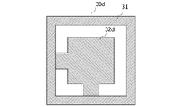
- FIG. 26 is a diagram showing an example of a conductor pattern in the fourth modification.
- the conductor pattern 30d of the radio wave absorbing sheet according to the fourth modification includes the loop antenna element 31 and one patch antenna element 32d inscribed in the loop antenna element 31.
- the patch antenna element 32d is inscribed on two adjacent sides of the four sides of the loop antenna element 31 formed in a rectangular frame shape.
- Simulations were performed for the third modification and the fourth modification to verify the radio wave absorption characteristics.
- the conditions set in the simulation are the same as the simulations of the first modification and the second modification described above.
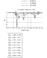
- FIG. 27 is a diagram illustrating the comparison results of the third modified example and the fourth modified example by simulation.
- the simulation results for the third comparative example are also illustrated.
- the vertical axis represents absorption efficiency (dB) and the horizontal axis represents frequency (GHz).
- the fourth modification high radio wave absorption characteristics are exhibited in the two frequency bands (2.4 GHz and 5.0 GHz) used in the wireless LAN. Further, in the fourth modification, it can be understood that the frequency band showing the peak of the radio wave absorption characteristic is added (the portion circled in FIG. 27). In other words, it can be said that the fourth modification is similar to the first modification in the radio wave absorption characteristics. Further, it can be understood that the third modification also shows the peak of the radio wave absorption characteristic at 2.1 GHz or 5.0 GHz.
- FIG. 28 is a Smith chart illustrating the comparison results of the third modified example and the fourth modified example by simulation. In FIG. 28, for reference, the simulation results for the third comparative example are also illustrated.
- the locus on the Smith chart is narrower than in the first modified example and the third comparative example. That is, it is considered that the resistance tends to be larger in the fourth modified example than in the third modified example and the third comparative example. Therefore, in the fourth modification, for example, it is conceivable to reduce the resistance by increasing the line width of the loop antenna element 31 and the patch antenna element 32a.
- FIG. 29 is a diagram illustrating the shape of the conductor pattern in the fifth modification.
- the conductor pattern 30e in the fifth modification includes three patch antenna elements 32e instead of the four patch antenna elements 32 of the conductor pattern 30 in the embodiment.
- the patch antenna element 32e is different from the patch antenna element 32 in that it does not have a through hole 33. That is, the disclosed technique can also employ a patch antenna element 32e that does not have a through hole 33.
- FIG. 30 is a diagram illustrating the shape of the conductor pattern in the fifth modification.
- the conductor pattern 30f in the fifth modification is different from the conductor pattern 30e in the fourth modification in that it includes two patch antenna elements 32e inscribed in each of the two opposing angles of the loop antenna element 31.
- FIG. 31 is a diagram illustrating the shape of the conductor pattern in the sixth modification.
- the conductor pattern 30g in the sixth modification is the same as the conductor pattern 30e in the fourth modification in that it includes two patch antenna elements 32e inscribed at both ends of one of the four sides of the loop antenna element 31. Is different.
- FIG. 32 is a diagram illustrating the shape of the conductor pattern in the seventh modification.
- the conductor pattern 30h in the seventh modification is different from the conductor pattern 30e in the fourth modification in that it includes one patch antenna element 32e inscribed in one of the four corners of the loop antenna element 31.
- FIG. 33 is a diagram illustrating the shape of the conductor pattern in the eighth modification.
- the conductor pattern 30i in the eighth modification is different from the conductor pattern 30 according to the embodiment in that it includes four patch antenna elements 32 inscribed in the center of each of the four sides of the loop antenna element 31. That is, in the conductor pattern 30i, the position of the patch antenna element 32 is different from that of the conductor pattern 30.
- FIG. 34 is a diagram illustrating the shape of the conductor pattern in the ninth modification.
- the conductor pattern 30j in the ninth modification is a loop antenna element 31a formed in a circular frame shape and four pieces arranged in a circular frame shape and inscribed in the loop antenna element 31a apart from each other.
- a patch antenna element 32f is provided.
- the patch antenna element 32f is formed in a circular shape and is provided with a through hole 33a that penetrates the patch antenna element 32f in the thickness direction. That is, the conductor pattern 30j differs from the conductor pattern 30 in the embodiment in the shapes of the loop antenna element 31a, the patch antenna element 32f, and the through hole 33a.
- the number of patch antenna elements 32f included in the conductor pattern 30j is not limited to four.
- the conductor pattern 30j may include three patch antenna elements 32f as illustrated in FIG. 35, or may include five or more or two or less patch antenna elements 32f.
- FIG. 36 is a diagram illustrating the shape of the conductor pattern in the tenth modification.
- the conductor pattern 30k in the tenth modification is different from the conductor pattern 30j in the ninth modification in that one patch antenna element 32g formed larger than the patch antenna element 32f is provided.
- FIG. 37 is a diagram illustrating the shape of the conductor pattern in the eleventh modification.
- the conductor pattern 30m in the eleventh modification is formed in the shape of a triangular frame and the loop antenna element 31b, and is arranged so as to be separated from each other and inscribed in the loop antenna element 31b.
- a patch antenna element 32h is provided.
- the patch antenna element 32h is formed in a triangular shape and is provided with a through hole 33b that penetrates the patch antenna element 32h in the thickness direction. That is, the shape of the loop antenna element 31a, the patch antenna element 32h, and the through hole 33b of the conductor pattern 30h is different from that of the conductor pattern 30 in the embodiment.
- FIG. 38 is a diagram illustrating the shape of the conductor pattern in the twelfth modification.
- the conductor pattern 30n in the twelfth modification includes three patch antenna elements 32 inscribed in the loop antenna element 31 and a patch antenna element 32i inscribed in the loop antenna element 31 and having a size different from that of the patch antenna element 32. If the radio wave absorbing sheet 1 employs the conductor pattern 30n provided with the patch antenna elements 32i having different sizes as described above, it can absorb radio waves in three or more frequency bands.
- a through hole may or may not be provided.
- the size of the through hole may be appropriately determined in consideration of matching with a radio wave of a desired frequency.
- FIG. 39 is a first diagram illustrating the arrangement of the conductor pattern on the radio wave absorbing sheet.
- a radio wave absorbing sheet 1 in which the conductor patterns 30j are arranged side by side on the front surface 11 of the dielectric layer 10 so as to have a substantially honeycomb structure is exemplified.
- conductor patterns other than the conductor pattern 30j may be arranged side by side on the front surface 11 of the dielectric layer 10 so as to have a honeycomb structure.
- FIG. 40 is a second diagram illustrating the arrangement of the conductor pattern on the radio wave absorbing sheet.
- FIG. 40 includes a first row in which conductor patterns 30 m formed in an overall triangular shape are arranged in a horizontal row with the vertices facing down, and a second row in which the conductor patterns 30m are arranged in a horizontal row with the vertices facing up.
- the vertices of the conductor pattern 30m arranged in the second row are arranged so as to be between adjacent vertices of the conductor pattern 30m arranged in the first row.
- ⁇ Usage example> By providing the radio wave absorbing sheet 1 described above between the lanes of the factory, for example, it is possible to suppress the leakage of radio waves from one lane to another. Further, the radio wave absorbing sheet 1 is provided at the boundary of each booth such as an exhibition hall, an aquarium, a museum, a zoo, etc., so that other boosts can provide different information in each booth by using wireless communication. By providing the radio wave absorption sheet 1 at the boundary of each department in the office, it is possible to suppress information leakage between departments due to the radio waves used for wireless communication reaching other departments.
- wireless LAN environments have been provided in public places such as waiting rooms at stations and airports, inside Shinkansen trains, inside restaurants, and coworking spaces.
- the radio wave absorbing sheet 1 By providing the radio wave absorbing sheet 1 at the boundary of seats or the like in such a public place, it is possible to suppress information leakage due to the radio waves used for wireless communication reaching other seats or the like.
- the radio wave absorbing sheet 1 is provided at the boundary of the space, so that such malfunction can be suppressed. ..
- the radio wave absorbing sheet 1 according to the present embodiment can be easily made thinner. Therefore, the radio wave absorbing sheet 1 can be easily used as a wallpaper of a room or superimposed on a seat surface or a backrest of a chair.
Landscapes
- Engineering & Computer Science (AREA)
- Microelectronics & Electronic Packaging (AREA)
- Waveguide Aerials (AREA)
- Details Of Aerials (AREA)
Priority Applications (2)
| Application Number | Priority Date | Filing Date | Title |
|---|---|---|---|
| JP2022556337A JP7685516B2 (ja) | 2020-10-22 | 2020-10-22 | 電波吸収体 |
| PCT/JP2020/039768 WO2022085164A1 (ja) | 2020-10-22 | 2020-10-22 | 電波吸収体 |
Applications Claiming Priority (1)
| Application Number | Priority Date | Filing Date | Title |
|---|---|---|---|
| PCT/JP2020/039768 WO2022085164A1 (ja) | 2020-10-22 | 2020-10-22 | 電波吸収体 |
Publications (1)
| Publication Number | Publication Date |
|---|---|
| WO2022085164A1 true WO2022085164A1 (ja) | 2022-04-28 |
Family
ID=81290259
Family Applications (1)
| Application Number | Title | Priority Date | Filing Date |
|---|---|---|---|
| PCT/JP2020/039768 Ceased WO2022085164A1 (ja) | 2020-10-22 | 2020-10-22 | 電波吸収体 |
Country Status (2)
| Country | Link |
|---|---|
| JP (1) | JP7685516B2 (https=) |
| WO (1) | WO2022085164A1 (https=) |
Citations (5)
| Publication number | Priority date | Publication date | Assignee | Title |
|---|---|---|---|---|
| JPH1117380A (ja) * | 1997-05-01 | 1999-01-22 | Tokai Univ | 電波吸収体 |
| JP2007073662A (ja) * | 2005-09-06 | 2007-03-22 | Mitsubishi Gas Chem Co Inc | 電波吸収体 |
| JP2011217205A (ja) * | 2010-03-31 | 2011-10-27 | Tokyo Keiki Inc | 平面アンテナ |
| JP2014110325A (ja) * | 2012-12-03 | 2014-06-12 | Sumitomo Electric Ind Ltd | 電磁波吸収体および光トランシーバ |
| JP2017092377A (ja) * | 2015-11-16 | 2017-05-25 | 富士通テン株式会社 | シールドカバー、デバイス |
-
2020
- 2020-10-22 JP JP2022556337A patent/JP7685516B2/ja active Active
- 2020-10-22 WO PCT/JP2020/039768 patent/WO2022085164A1/ja not_active Ceased
Patent Citations (5)
| Publication number | Priority date | Publication date | Assignee | Title |
|---|---|---|---|---|
| JPH1117380A (ja) * | 1997-05-01 | 1999-01-22 | Tokai Univ | 電波吸収体 |
| JP2007073662A (ja) * | 2005-09-06 | 2007-03-22 | Mitsubishi Gas Chem Co Inc | 電波吸収体 |
| JP2011217205A (ja) * | 2010-03-31 | 2011-10-27 | Tokyo Keiki Inc | 平面アンテナ |
| JP2014110325A (ja) * | 2012-12-03 | 2014-06-12 | Sumitomo Electric Ind Ltd | 電磁波吸収体および光トランシーバ |
| JP2017092377A (ja) * | 2015-11-16 | 2017-05-25 | 富士通テン株式会社 | シールドカバー、デバイス |
Also Published As
| Publication number | Publication date |
|---|---|
| JP7685516B2 (ja) | 2025-05-29 |
| JPWO2022085164A1 (https=) | 2022-04-28 |
Similar Documents
| Publication | Publication Date | Title |
|---|---|---|
| US10892547B2 (en) | Inconspicuous multi-directional antenna system configured for multiple polarization modes | |
| US8164506B2 (en) | Electromagnetic absorber using resistive material | |
| US12562496B2 (en) | Meta-structure based reflectarrays for enhanced wireless applications | |
| JP7635917B2 (ja) | アンテナユニット及び窓ガラス | |
| CN105322291B (zh) | 微带阵列天线 | |
| KR20220043213A (ko) | 빔 형성 시스템을 위한 메타 구조의 무선 인프라구조 | |
| CN101548434A (zh) | 用于移动通信的双波段双极化基站天线 | |
| CN205231255U (zh) | 一种三频基站天线 | |
| US20220416414A1 (en) | Antenna unit and window glass | |
| WO2006088063A1 (ja) | 電波遮蔽体 | |
| WO2022264973A1 (ja) | アンテナ装置および建物用窓ガラス | |
| CN105140628B (zh) | 一种微带全向天线及通信器件 | |
| JP4744949B2 (ja) | 電波遮蔽装置 | |
| WO2022085164A1 (ja) | 電波吸収体 | |
| JP6965989B2 (ja) | 電磁波伝搬制御部材、電磁波伝搬制御構造体、電磁波伝搬制御部材付きサッシ及び窓構造体 | |
| CN205488477U (zh) | 高增益窄波束电梯天线 | |
| CN117616635A (zh) | 包括辐射器阵列和折射器件的天线装置 | |
| JP3180899B2 (ja) | 電波遮蔽面状体及び建物内電波遮蔽域 | |
| JP2015220411A (ja) | 電波吸収体及び電波暗室 | |
| JP6837932B2 (ja) | アンテナ | |
| WO2024029325A1 (ja) | 反射パネル、これを用いた電磁波反射装置、及び電磁波反射フェンス | |
| CN206673109U (zh) | 一种基站阵列天线 | |
| CN204668463U (zh) | 全向天线 | |
| TW202410552A (zh) | 反射板、使用其之電磁波反射裝置、及電磁波反射柵 | |
| US20240339756A1 (en) | Planar transparent antenna structure |
Legal Events
| Date | Code | Title | Description |
|---|---|---|---|
| 121 | Ep: the epo has been informed by wipo that ep was designated in this application |
Ref document number: 20958716 Country of ref document: EP Kind code of ref document: A1 |
|
| ENP | Entry into the national phase |
Ref document number: 2022556337 Country of ref document: JP Kind code of ref document: A |
|
| NENP | Non-entry into the national phase |
Ref country code: DE |
|
| 122 | Ep: pct application non-entry in european phase |
Ref document number: 20958716 Country of ref document: EP Kind code of ref document: A1 |