WO2022071549A1 - Detection device - Google Patents
Detection device Download PDFInfo
- Publication number
- WO2022071549A1 WO2022071549A1 PCT/JP2021/036348 JP2021036348W WO2022071549A1 WO 2022071549 A1 WO2022071549 A1 WO 2022071549A1 JP 2021036348 W JP2021036348 W JP 2021036348W WO 2022071549 A1 WO2022071549 A1 WO 2022071549A1
- Authority
- WO
- WIPO (PCT)
- Prior art keywords
- detector
- radiation
- container
- detection device
- drift electrode
- Prior art date
Links
- 238000001514 detection method Methods 0.000 title claims abstract description 134
- 230000005855 radiation Effects 0.000 claims abstract description 239
- 239000000463 material Substances 0.000 claims description 14
- 239000003463 adsorbent Substances 0.000 claims description 12
- 125000006850 spacer group Chemical group 0.000 claims description 8
- 239000004065 semiconductor Substances 0.000 claims description 5
- 230000004048 modification Effects 0.000 description 71
- 238000012986 modification Methods 0.000 description 71
- 239000007789 gas Substances 0.000 description 15
- 229910052751 metal Inorganic materials 0.000 description 15
- 239000002184 metal Substances 0.000 description 15
- 230000005684 electric field Effects 0.000 description 12
- 239000000758 substrate Substances 0.000 description 8
- 230000009471 action Effects 0.000 description 7
- 229910052782 aluminium Inorganic materials 0.000 description 6
- XAGFODPZIPBFFR-UHFFFAOYSA-N aluminium Chemical compound [Al] XAGFODPZIPBFFR-UHFFFAOYSA-N 0.000 description 6
- 230000005484 gravity Effects 0.000 description 6
- PXHVJJICTQNCMI-UHFFFAOYSA-N Nickel Chemical compound [Ni] PXHVJJICTQNCMI-UHFFFAOYSA-N 0.000 description 5
- 239000010949 copper Substances 0.000 description 4
- 230000006837 decompression Effects 0.000 description 4
- 230000000694 effects Effects 0.000 description 4
- 239000010931 gold Substances 0.000 description 4
- KDLHZDBZIXYQEI-UHFFFAOYSA-N Palladium Chemical compound [Pd] KDLHZDBZIXYQEI-UHFFFAOYSA-N 0.000 description 3
- 229910045601 alloy Inorganic materials 0.000 description 3
- 239000000956 alloy Substances 0.000 description 3
- 230000003321 amplification Effects 0.000 description 3
- 239000004020 conductor Substances 0.000 description 3
- 230000007547 defect Effects 0.000 description 3
- 238000010438 heat treatment Methods 0.000 description 3
- 239000012212 insulator Substances 0.000 description 3
- 238000005259 measurement Methods 0.000 description 3
- 238000003199 nucleic acid amplification method Methods 0.000 description 3
- 239000004033 plastic Substances 0.000 description 3
- 229920003023 plastic Polymers 0.000 description 3
- BASFCYQUMIYNBI-UHFFFAOYSA-N platinum Chemical compound [Pt] BASFCYQUMIYNBI-UHFFFAOYSA-N 0.000 description 3
- 239000010936 titanium Substances 0.000 description 3
- 229910000838 Al alloy Inorganic materials 0.000 description 2
- XKRFYHLGVUSROY-UHFFFAOYSA-N Argon Chemical compound [Ar] XKRFYHLGVUSROY-UHFFFAOYSA-N 0.000 description 2
- CURLTUGMZLYLDI-UHFFFAOYSA-N Carbon dioxide Chemical compound O=C=O CURLTUGMZLYLDI-UHFFFAOYSA-N 0.000 description 2
- RYGMFSIKBFXOCR-UHFFFAOYSA-N Copper Chemical compound [Cu] RYGMFSIKBFXOCR-UHFFFAOYSA-N 0.000 description 2
- BQCADISMDOOEFD-UHFFFAOYSA-N Silver Chemical compound [Ag] BQCADISMDOOEFD-UHFFFAOYSA-N 0.000 description 2
- RTAQQCXQSZGOHL-UHFFFAOYSA-N Titanium Chemical compound [Ti] RTAQQCXQSZGOHL-UHFFFAOYSA-N 0.000 description 2
- QVGXLLKOCUKJST-UHFFFAOYSA-N atomic oxygen Chemical compound [O] QVGXLLKOCUKJST-UHFFFAOYSA-N 0.000 description 2
- 239000003990 capacitor Substances 0.000 description 2
- 239000011651 chromium Substances 0.000 description 2
- 229910052802 copper Inorganic materials 0.000 description 2
- 238000009826 distribution Methods 0.000 description 2
- 238000010292 electrical insulation Methods 0.000 description 2
- -1 for example Inorganic materials 0.000 description 2
- PCHJSUWPFVWCPO-UHFFFAOYSA-N gold Chemical compound [Au] PCHJSUWPFVWCPO-UHFFFAOYSA-N 0.000 description 2
- 229910052737 gold Inorganic materials 0.000 description 2
- 238000004519 manufacturing process Methods 0.000 description 2
- VNWKTOKETHGBQD-UHFFFAOYSA-N methane Chemical compound C VNWKTOKETHGBQD-UHFFFAOYSA-N 0.000 description 2
- 238000000034 method Methods 0.000 description 2
- 229910052759 nickel Inorganic materials 0.000 description 2
- 239000001301 oxygen Substances 0.000 description 2
- 229910052760 oxygen Inorganic materials 0.000 description 2
- 230000008569 process Effects 0.000 description 2
- 230000000171 quenching effect Effects 0.000 description 2
- 239000010948 rhodium Substances 0.000 description 2
- 238000004904 shortening Methods 0.000 description 2
- 229910052709 silver Inorganic materials 0.000 description 2
- 239000004332 silver Substances 0.000 description 2
- 229910052719 titanium Inorganic materials 0.000 description 2
- XLYOFNOQVPJJNP-UHFFFAOYSA-N water Chemical compound O XLYOFNOQVPJJNP-UHFFFAOYSA-N 0.000 description 2
- SKJCKYVIQGBWTN-UHFFFAOYSA-N (4-hydroxyphenyl) methanesulfonate Chemical compound CS(=O)(=O)OC1=CC=C(O)C=C1 SKJCKYVIQGBWTN-UHFFFAOYSA-N 0.000 description 1
- VYZAMTAEIAYCRO-UHFFFAOYSA-N Chromium Chemical compound [Cr] VYZAMTAEIAYCRO-UHFFFAOYSA-N 0.000 description 1
- 229920002430 Fibre-reinforced plastic Polymers 0.000 description 1
- ZOKXTWBITQBERF-UHFFFAOYSA-N Molybdenum Chemical compound [Mo] ZOKXTWBITQBERF-UHFFFAOYSA-N 0.000 description 1
- VYPSYNLAJGMNEJ-UHFFFAOYSA-N Silicium dioxide Chemical compound O=[Si]=O VYPSYNLAJGMNEJ-UHFFFAOYSA-N 0.000 description 1
- ATJFFYVFTNAWJD-UHFFFAOYSA-N Tin Chemical compound [Sn] ATJFFYVFTNAWJD-UHFFFAOYSA-N 0.000 description 1
- 229910021536 Zeolite Inorganic materials 0.000 description 1
- HCHKCACWOHOZIP-UHFFFAOYSA-N Zinc Chemical compound [Zn] HCHKCACWOHOZIP-UHFFFAOYSA-N 0.000 description 1
- QCWXUUIWCKQGHC-UHFFFAOYSA-N Zirconium Chemical compound [Zr] QCWXUUIWCKQGHC-UHFFFAOYSA-N 0.000 description 1
- 229910052786 argon Inorganic materials 0.000 description 1
- 230000002238 attenuated effect Effects 0.000 description 1
- 229910002092 carbon dioxide Inorganic materials 0.000 description 1
- 239000001569 carbon dioxide Substances 0.000 description 1
- 239000003985 ceramic capacitor Substances 0.000 description 1
- 229910052804 chromium Inorganic materials 0.000 description 1
- HNPSIPDUKPIQMN-UHFFFAOYSA-N dioxosilane;oxo(oxoalumanyloxy)alumane Chemical compound O=[Si]=O.O=[Al]O[Al]=O HNPSIPDUKPIQMN-UHFFFAOYSA-N 0.000 description 1
- 239000011151 fibre-reinforced plastic Substances 0.000 description 1
- 230000003993 interaction Effects 0.000 description 1
- 150000002739 metals Chemical class 0.000 description 1
- 229910052750 molybdenum Inorganic materials 0.000 description 1
- 239000011733 molybdenum Substances 0.000 description 1
- 229910052756 noble gas Inorganic materials 0.000 description 1
- 229910052763 palladium Inorganic materials 0.000 description 1
- 239000002245 particle Substances 0.000 description 1
- 230000000149 penetrating effect Effects 0.000 description 1
- 229910052697 platinum Inorganic materials 0.000 description 1
- 238000010791 quenching Methods 0.000 description 1
- 230000009467 reduction Effects 0.000 description 1
- 239000011347 resin Substances 0.000 description 1
- 229920005989 resin Polymers 0.000 description 1
- 229910052703 rhodium Inorganic materials 0.000 description 1
- MHOVAHRLVXNVSD-UHFFFAOYSA-N rhodium atom Chemical compound [Rh] MHOVAHRLVXNVSD-UHFFFAOYSA-N 0.000 description 1
- 239000000741 silica gel Substances 0.000 description 1
- 229910002027 silica gel Inorganic materials 0.000 description 1
- 229910052715 tantalum Inorganic materials 0.000 description 1
- GUVRBAGPIYLISA-UHFFFAOYSA-N tantalum atom Chemical compound [Ta] GUVRBAGPIYLISA-UHFFFAOYSA-N 0.000 description 1
- WFKWXMTUELFFGS-UHFFFAOYSA-N tungsten Chemical compound [W] WFKWXMTUELFFGS-UHFFFAOYSA-N 0.000 description 1
- 229910052721 tungsten Inorganic materials 0.000 description 1
- 239000010937 tungsten Substances 0.000 description 1
- 229910052724 xenon Inorganic materials 0.000 description 1
- FHNFHKCVQCLJFQ-UHFFFAOYSA-N xenon atom Chemical compound [Xe] FHNFHKCVQCLJFQ-UHFFFAOYSA-N 0.000 description 1
- 239000010457 zeolite Substances 0.000 description 1
- 229910052725 zinc Inorganic materials 0.000 description 1
- 239000011701 zinc Substances 0.000 description 1
- 229910052726 zirconium Inorganic materials 0.000 description 1
Images


Classifications
-
- G—PHYSICS
- G01—MEASURING; TESTING
- G01T—MEASUREMENT OF NUCLEAR OR X-RADIATION
- G01T1/00—Measuring X-radiation, gamma radiation, corpuscular radiation, or cosmic radiation
- G01T1/16—Measuring radiation intensity
- G01T1/185—Measuring radiation intensity with ionisation chamber arrangements
Definitions
- the embodiment of the present disclosure relates to a detection device that detects radiation.
- a detection device for detecting radiation scattered by Compton and electrons generated by Compton scattering includes a container containing gas, a drift electrode and an electron detector facing each other inside the container, and a radiation detector located outside the container.
- the information is, for example, the position where the Compton scattering occurred, the track of the rebounding electron generated by the Compton scattering, the energy of the radiation scattered by the Compton, and the like.
- the drift electrode, the electron detector, and the radiation detector it may not be possible to obtain these information accurately.
- the radiation scattered in Compton inside the container passes through the electron detector, the container, and the air outside the container, and then enters the radiation detector.
- interaction can occur between the radiation and the electron detector, the container, and the air outside the container.
- the radiation is photoelectrically absorbed or that radiation having different energies is generated.
- Compton scattering occurs in the electron detector, the container, and the air outside the container. When these phenomena occur, the energy, position, etc. of the radiation detected by the radiation detector may not correspond to the Compton scattering generated between the drift electrode and the electron detector. Therefore, variations in detection results, errors, and the like are likely to occur.
- An embodiment of the present disclosure is an object of the present invention to provide a detection device capable of effectively solving such a problem.
- One embodiment of the present disclosure is a detection device that detects radiation.
- a container containing a gas including a first part, a second part facing the first part in the first direction, and a side part extending from the first part toward the second part.
- An electron detector located inside the container to detect electrons generated by Compton scattering
- a drift electrode located inside the container on the side of the second part of the electron detector and facing the electron detector. It is a detection device including a radiation detector that is located on the side of the second part of the drift electrode and detects scattered radiation.
- the radiation detector may be located inside the container.
- the radiation detector may be located outside the container.
- the first part has an outer surface that spreads flat in a range overlapping the electron detector when viewed along a direction in which the electron detector and the drift electrode face each other. It may be included.
- the distance between the inner surface of the first part and the electronic detector may be 10 mm or less.
- One embodiment of the present disclosure is a detection device that detects radiation.
- a container containing a gas including a first part, a second part facing the first part in the first direction, and a side part extending from the first part toward the second part.
- An electron detector located inside the container to detect electrons generated by Compton scattering
- a drift electrode located inside the container on the side of the first part of the electron detector and facing the electron detector.
- the radiation detector may be located inside the container.
- the radiation detector may be located outside the container.
- the first part includes an outer surface that spreads flat in a range overlapping the drift electrode when viewed along a direction in which the electron detector and the drift electrode face each other. You may be.
- the distance between the inner surface of the first part and the drift electrode may be 10 mm or more and 100 mm or less.
- the drift electrode may include a plurality of through holes.
- One embodiment of the present disclosure is a detection device that detects radiation.
- a container containing a gas including a first part, a second part facing the first part in the first direction, and a side part extending from the first part toward the second part.
- An electron detector located inside the container to detect electrons generated by Compton scattering
- a drift electrode located inside the container and facing the electron detector in a direction intersecting the first direction, It is a detection device including a radiation detector that is closer to the second part than the first part and detects scattered radiation.
- the radiation detector may be located inside the container.
- the radiation detector may be located outside the container.
- the detection device may be located between the electron detector and the drift electrode, and may include the electron detector and an electronic amplifier facing the drift electrode.
- the electron detector comprises a plurality of collection electrodes.
- the electronic amplifier includes a front surface and a back surface, a base material having a through hole overlapping the collection electrode in a direction facing the drift electrode, a first electrode located on the front surface, and a first electrode located on the back surface.
- the second electrode may be included.
- the detection device comprises a plurality of ring electrodes arranged along a direction in which the electron detector and the drift electrode face each other, and a spacer located between two adjacent ring electrodes. It may be provided with an auxiliary drift electrode including.
- the detection device comprises a plurality of ring electrodes arranged along a direction in which the electron detector and the drift electrode face each other, and a spacer located between two adjacent ring electrodes.
- An auxiliary drift electrode including the auxiliary drift electrode and a relay board for supporting the auxiliary drift electrode and the electron detector may be provided.
- the drift electrode may be attached to the auxiliary drift electrode so as to face the electron detector.
- the relay board may be arranged on the second part.
- the radiation detector may include a scintillator that is excited by the scattered radiation to emit fluorescence, and a photodetector that detects the fluorescence.
- the radiation detector may include a semiconductor detection element for detecting the scattered radiation.
- the side portion of the container may have a cylindrical shape.
- the detection device may include an adsorbent located inside the container.
- the detection device may include a circulation path connected to the container and a pump and a filter inserted in the circulation path.
- the detection accuracy of the radiation detector can be improved.
- the numerical range of the parameter is any one upper limit candidate and any one lower limit value. It may be configured by combining with the candidates of.
- “Parameter B may be, for example, A1 or more, A2 or more, or A3 or more. Parameter B may be, for example, A4 or less, A5 or less, or A6 or less. It may be. " In this case, the numerical range of the parameter B may be A1 or more and A4 or less, A1 or more and A5 or less, A1 or more and A6 or less, or A2 or more and A4 or less. It may be A2 or more and A5 or less, A2 or more and A6 or less, A3 or more and A4 or less, A3 or more and A5 or less, or A3 or more and A6 or less.
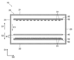
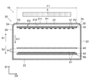
- FIG. 1 is a perspective view showing an example of the detection device 10.
- FIG. 2 is a cross-sectional view of the detection device 10 of FIG.
- the detection device 10 includes a container 20, an electron detector 30, a drift electrode 40, and a radiation detector 50 located inside the container 20.
- the container 20 is, for example, a chamber. At least a rare gas such as argon or xenon is contained in the container 20. In addition to the noble gas, a quenching gas having a quenching action such as carbon dioxide and methane may be contained in the container 20.
- the container 20 includes a first surface 21, a second surface 22 facing the first surface 21 in the first direction D1, and a side surface 23 extending from the first surface 21 toward the second surface 22.
- the detection device 10 is supposed to detect the radiation incident on the inside of the container 20 through the first surface 21.
- the container 20 may be placed so that the second surface 22 faces or is in contact with a surface such as a floor or a table.
- the container 20 may have a cylindrical shape. That is, the side surface 23 may have a circular cross section.
- the container 20 may have a shape other than a cylindrical shape, for example, a cube or a rectangular parallelepiped shape.
- the first surface 21 may be curved so as to be convex toward the outside of the container 20.
- the object that emits radiation is located outside the container 20.
- the first surface 21 is the surface of the container closest to the object. In the following description, the first surface 21 is also referred to as a first part 21.
- the second surface 22 is also referred to as a second part 22.
- the side surface 23 is also referred to as a side portion 23.
- the material of the container 20 is preferably one that easily transmits radiation. This makes it possible to prevent radiation from being absorbed or scattered by the container 20 while passing through the container 20.
- the container 20 may contain, for example, plastic or metal.
- the plastic may be a fiber reinforced plastic.
- the container 20 may be composed of a single metal element or may be composed of an alloy.
- the metal for example, aluminum or an aluminum alloy can be used.
- a metal having a specific gravity of less than 4 may be used.
- the thickness of the container 20 is, for example, 1 mm or more, may be 5 mm or more, or may be 10 mm or more.
- the thickness of the container 20 is, for example, 30 mm or less, 25 mm or less, or 20 mm or less.
- the thickness of the container 20 is, for example, 2 mm or more, may be 3 mm or more, or may be 5 mm or more.
- the thickness of the container 20 is, for example, 20 mm or less, may be 15 mm or less, or may be 10 mm or less.
- the electron detector 30, the drift electrode 40, and the radiation detector 50 are arranged in this order on the side from the first part 21 to the second part 22. That is, the drift electrode 40 is located closer to the second part 22 than the electron detector 30. The radiation detector 50 is located closer to the second part 22 than the drift electrode 40.
- the component A is located on the side of the second part 22 with respect to the component B
- the arrow S2 indicates the direction from the first part 21 to the second part 22.
- the distance from the component B to the second part 22 may be longer or shorter than the distance from the component B to the component A.
- the electron detector 30 may be closer to the first part 21 than to the second part 22.
- the drift electrode 40 and the radiation detector 50 may be closer to the second part 22 than to the first part 21.
- the electron detector 30, the drift electrode 40 and the radiation detector 50 will be described in detail.
- Compton scattering may occur when the radiation incident inside the container 20 collides with the gas.
- Compton scattering occurs, rebound electrons are generated.
- ionized electrons are generated along the tracks of the rebounding electrons.
- the electron detector 30 detects ionized electrons. By detecting the ionized electrons, the track and energy of the rebounding electrons can be calculated.
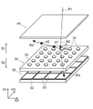
- FIG. 3 is a perspective view showing an example of the electronic detector 30.
- the electron detector 30 may include a plurality of collection electrodes 31 and a support substrate 32 that supports the collection electrodes 31.
- the collection electrode 31 faces the drift electrode 40.
- the support substrate 32 includes a surface extending in a direction intersecting the first direction D1.
- the collecting electrode 31 detects the ionized electrons attracted to the electron detector 30 by the electric field.
- the plurality of collection electrodes 31 may be arranged in a direction intersecting the first direction D1.
- the support substrate 32 may include a surface extending in a direction orthogonal to the first direction D1.
- the plurality of collection electrodes 31 may be arranged in the second direction D2 and the third direction D3 orthogonal to the first direction D1.
- the second direction D2 and the third direction D3 may be orthogonal to each other.
- the collection electrode 31 contains a conductive material.
- the materials of the collection electrode 31 include copper (Cu), gold (Au), silver (Ag), platinum (Pt), palladium (Pd), rhodium (Rh), tin (Sn), aluminum (Al), and nickel (Nickel).
- Metals such as Ni), chromium (Cr), titanium (Ti), molybdenum (Mo), tungsten (W), and tantalum (Ta) or alloys using these can be used.
- a metal having high conductivity such as copper (Cu), gold (Au), silver (Ag) is used.
- the electrons detected by the collection electrode 31 are processed as an electric signal.
- the electronic detector 30 may include a circuit, wiring, and the like for processing an electric signal.
- the electrical signal may be transmitted to the outside of the container 20 via, for example, a cable (not shown) connected to the electronic detector 30, a hermetic connector, a wiring board, or the like.
- a plurality of electron detectors 30 may be arranged in the second direction D2 or the third direction D3. As a result, the area where electrons can be detected can be expanded.
- the drift electrode 40 is arranged so as to face the electron detector 30.
- the drift electrode 40 faces the electron detector 30 in the first direction D1. That is, the drift electrode 40 includes a surface extending in a direction orthogonal to the first direction D1.
- the drift electrode 40 has a potential lower than the potential of the collection electrode 31 of the electron detector 30. Therefore, as shown in FIG. 2, an electric field E1 from the electron detector 30 toward the drift electrode 40 is generated between the electron detector 30 and the drift electrode 40.
- the ionized electrons associated with the rebound electrons generated by Compton scattering are attracted to the electron detector 30 side by the electric field E1.
- the drift electrode 40 contains a conductive material.
- the drift electrode 40 includes a metal having a specific gravity of less than 4, such as aluminum and an aluminum alloy. As a result, it is possible to suppress the influence of the radiation passing through the drift electrode 40 on the drift electrode 40 as compared with the case where the drift electrode 40 contains a metal having a large specific gravity.
- the thickness of the drift electrode 40 is, for example, 0.01 mm or more, may be 0.1 mm or more, or may be 0.3 mm or more.
- the thickness of the drift electrode 40 is, for example, 2.0 mm or less, may be 1.0 mm or less, or may be 0.5 mm or less. The smaller the thickness of the drift electrode 40, the more the radiation passing through the drift electrode 40 can be suppressed from being affected by the drift electrode 40.
- the radiation detector 50 detects scattered radiation.
- the radiation scattered between the electron detector 30 and the drift electrode 40 is detected by the radiation detector 50 after passing through the drift electrode 40.
- the radiation detector 50 can detect the position and energy of the radiation that has reached the radiation detector 50.
- FIG. 4 is a perspective view showing an example of the radiation detector 50.
- the radiation detector 50 may include a plurality of detection elements 51 and a circuit board 52 that supports the detection elements 51.
- the plurality of detection elements 51 may be arranged in a direction intersecting the first direction D1.
- the plurality of detection elements 51 may be arranged in the second direction D2 and the third direction D3 orthogonal to the first direction D1.
- the configuration of the detection element 51 is arbitrary as long as radiation can be detected.
- the detection element 51 may include a scintillator that is excited by scattered radiation to emit fluorescence, and a photodetector that detects fluorescence.
- the photodetector may include, for example, an avalanche photodiode.
- the detection element 51 may include a semiconductor detection element that detects the scattered radiation.
- the semiconductor detection element may include, for example, a semiconductor containing zinc telluride zinc cadonium.
- the radiation detector 50 has a first detection element 51 capable of detecting radiation having energy within the first range and a second detection element 51 capable of detecting radiation having energy within a second range different from the first range. And may be included. This makes it possible to expand the range of radiation energy that can be detected by the radiation detector 50.
- the radiation detected by the detection element 51 is processed as an electronic signal by the circuit board 52.
- the circuit board 52 may include a circuit for processing an electric signal, wiring, and the like.
- the electric signal may be transmitted to the outside of the container 20 via, for example, a cable (not shown) connected to the circuit board 52, a hermetic connector, a wiring board, or the like.
- the radiation detector 50 is electrically isolated from the drift electrode 40.
- the distance K1 between the radiation detector 50 and the drift electrode 40 is set so that electrical insulation is ensured.
- a gas, an insulator, or the like may be located between the drift electrode 40 and the radiation detector 50. As a result, it is possible to suppress the occurrence of defects such as electric discharge between the drift electrode 40 and the radiation detector 50.
- a plurality of radiation detectors 50 may be arranged in the second direction D2 or the third direction D3. This makes it possible to expand the area where radiation can be detected.
- the electrical components located inside the container 20, such as the electron detector 30, the drift electrode 40, and the radiation detector 50, are arranged so as not to cause a defect such as an electric discharge with the inner surface of the container 20.
- the arrangement and potential of the electric parts are determined so that the electric field generated between the electric parts located inside the container 20 and the inner surface of the container 20 is 2.5 kV / cm or less.
- the inside of the container used for processing is controlled to have a pressure atmosphere lower than the atmospheric pressure, and the electric parts are heated inside the container.
- the pressure of the atmosphere is, for example, 0.1 atm or less.
- the pressure may be maintained below 0.1 atm by exhausting the inside of the container during the reduced pressure baking process.
- the heating temperature is, for example, 60 ° C. or higher, and may be 100 ° C. or higher.
- the heating temperature may be 125 ° C. or lower.
- the heating time may be 2 hours or more, or 12 hours or more.
- the container 20 of the detection device 10 may be similarly subjected to the first decompression baking treatment.
- the electric component subjected to the first decompression baking process is placed inside the container 20.
- the electric component may be subjected to a second decompression baking treatment inside the container 20.
- the drift electrode 40, the radiation detector 50, the cable, and the connector parts that do not easily generate outgas are used.
- a component including a hollow portion such as an aluminum electrolytic capacitor tends to generate outgas.
- a monolithic ceramic capacitor instead of the aluminum electrolytic capacitor.
- reference numeral R1 represents radiation that has passed through the first part 21 of the container 20 and has entered the inside of the container 20.
- Radiation R1 is, for example, charged particles, gamma rays, X-rays, neutrons, ultraviolet light, or the like. After passing through the electron detector 30, the radiation R1 reaches the space between the electron detector 30 and the drift electrode 40.
- Reference numeral R2 represents the radiation that has reached the space between the electron detector 30 and the drift electrode 40. The energy of radiation R2 may be lower than that of radiation R1 due to the scattering and attenuation that occurs as it passes through the electron detector 30.
- Reference numeral R3 represents scattered radiation.
- the radiation R3 reaches the radiation detector 50 after passing through the drift electrode 40.
- Reference numeral R4 represents the radiation that has reached the radiation detector 50.
- the energy of the radiation R4 may be lower than the energy of the radiation R3 due to the scattering and attenuation that occur as it passes through the drift electrode 40.
- Radiation R4 is detected by one of the plurality of detection elements 51. Thereby, the arrival position and energy of the radiation R4 can be calculated.
- the symbol R5 represents a rebound electron generated by Compton scattering.
- An electron cloud is formed in the track of the rebound electron R5.
- Each electron of the electron cloud is attracted to the electron detector 30 side by the electric field E1.
- the electrons e1 and e2 generated in order along the track of the rebound electron R5 are attracted to the electron detector 30 side.
- the electrons e1 and e2 are detected by the collection electrode 31 corresponding to the positions of the electrons e1 and e2. Thereby, the positions and energies of the electrons e1 and e2 can be calculated.
- the track and energy of the rebound electron R5 and the scattering point P can be calculated.
- the radiation detector 50 is located inside the container 20. Therefore, as compared with the case where the radiation detector 50 is located outside the container 20, it is possible to suppress the occurrence of radiation scattering, attenuation, and the like before reaching the radiation detector 50. Therefore, it is possible to obtain more accurate information about the radiation R3 scattered in the space between the electron detector 30 and the drift electrode 40.
- the radiation detector 50 faces the drift electrode 40.
- the thickness of the drift electrode 40 is small and the specific gravity of the metal constituting the drift electrode 40 is small, the radiation passing through the drift electrode 40 is not easily affected by the drift electrode 40.
- This can also contribute to reducing the difference between the energy of the radiation R4 reaching the radiation detector 50 and the energy of the scattered radiation R3. Further, it can contribute to reducing the difference between the radiation dose of the radiation R4 reaching the radiation detector 50 and the radiation dose of the scattered radiation R3. Therefore, more accurate information about the scattered radiation R3 can be obtained.
- This embodiment is particularly useful when the energies of the radiations R1 and R2 before being scattered are unknown.
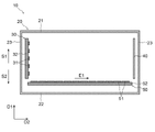
- FIG. 6 is a cross-sectional view showing the detection device 10 according to the first modification.
- the detection device 10 may include an electron amplifier 60 located between the electron detector 30 and the drift electrode 40.
- the electron amplifier 60 is arranged so as to face the electron detector 30 and the drift electrode 40, for example, in the first direction D1.
- the electron amplifier 60 is configured to cause electron avalanche amplification.
- the electronic amplifier 60 includes a base material 63 including a front surface 631 and a back surface 632, a first electrode 61 located on the front surface 631, and a second electrode 62 located on the back surface 632.
- the first electrode 61 faces the electron detector 30.
- the second electrode 62 faces the drift electrode 40.
- the base material 63 is formed with a plurality of through holes 64 penetrating from the front surface 631 to the back surface 632. As shown in FIG. 6, the through hole 64 overlaps with the collection electrode 31 of the electron detector 30 in the direction facing the drift electrode 40, for example, in the first direction D1.
- a plurality of collection electrodes 31 may overlap with one through hole 64.
- the potential of the second electrode 62 is higher than the potential of the drift electrode 40. Therefore, an electric field E2 from the second electrode 62 toward the drift electrode 40 is generated between the second electrode 62 and the drift electrode 40.
- the potential of the first electrode 61 is higher than the potential of the second electrode 62. Therefore, an electric field E3 from the first electrode 61 to the second electrode 62 is generated between the first electrode 61 and the second electrode 62.
- the electrons attracted to the electron amplifier 60 collide with the gas and ionize the gas.
- the ionized electrons are attracted to the first electrode 61 side as an electron group while being amplified like an avalanche inside the through hole 64.
- the electrons that have passed through the through hole 64 are detected by the collection electrode 31. According to this modification, the amount of electrons to be measured increases by using the electron amplifier 60. Therefore, the position of an electron or the like can be detected with higher accuracy.
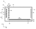
- FIG. 7 is a cross-sectional view showing the detection device 10 according to the second modification.
- the detection device 10 may include an auxiliary drift electrode 70 located between the electron detector 30 and the drift electrode 40.
- the auxiliary drift electrode 70 includes a surface 71 extending in a direction in which the electron detector 30 and the drift electrode 40 face each other.
- the surface 71 extends in the first direction D1.
- the auxiliary drift electrode 70 is provided to enhance the uniformity of the electric field distribution between the electron detector 30 and the drift electrode 40.
- the auxiliary drift electrode 70 may surround the space between the electron detector 30 and the drift electrode 40.
- the auxiliary drift electrode 70 may include a plurality of electrodes arranged along the first direction D1.
- the auxiliary drift electrode 70 may have a so-called cage-like structure in which a space between the electron detector 30 and the drift electrode 40 is surrounded by a plurality of electrodes.
- the auxiliary drift electrode 70 may be fixed by a material such as a resin having an insulating property.
- the auxiliary drift electrode 70 contains a conductive material like the drift electrode 40.
- the auxiliary drift electrode 70 may contain a metal having a specific gravity of less than 4, such as aluminum.
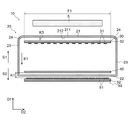
- FIG. 8 is a cross-sectional view showing the detection device 10 according to the third modification.
- the radiation detector 50 may be located outside the container 20.
- the radiation detector 50 may be located outside the second part 22.
- the radiation detector 50 may face the drift electrode 40 with the second part 22 interposed therebetween.
- the radiation detector 50 by arranging the radiation detector 50 outside the container 20, it is possible to prevent the outgas generated from the radiation detector 50 from affecting the environment inside the container 20. Thereby, for example, the density of the electron cloud formed in the track of the rebound electron R5 can be further increased. Further, when the electronic amplifier 60 is provided inside the container 20, the amplification of electrons by the electronic amplifier 60 can be further promoted.
- the radiation R3 scattered in the space between the electron detector 30 and the drift electrode 40 reaches the radiation detector 50 after passing through the drift electrode 40 and the second part 22 of the container 20. .. It is preferable that the thickness of the second part 22 is small in order to suppress the scattering and attenuation of radiation in the second part 22.
- FIG. 9 is a cross-sectional view showing the detection device 10 according to the fourth modification.
- the detection device 10 may include an adsorbent 81 located inside the container 20.
- the adsorbent 81 can adsorb outgas generated from an electric component located inside the container 20.
- the adsorbent 81 can adsorb water vapor, oxygen, and the like.
- the adsorbent 81 is, for example, a getter material of an active metal or alloy such as titanium or zirconium, an adsorbent material such as zeolite or silica gel, or a getter pump.
- the adsorbent 81 is arranged at a position where it does not interfere with radiation.
- the adsorbent 81 may be arranged on the side portion 23 of the container 20.
- FIG. 10 is a cross-sectional view showing the detection device 10 according to the fifth modification.
- the detection device 10 may include a device for removing outgas generated from an electric component located inside the container 20.
- the detection device 10 may include a circulation path 82 connected to the container 20 and a pump 83 and a filter 84 inserted in the circulation path 82.
- the pump 83 sucks the gas inside the container 20 into the circulation path 82.
- the filter 84 removes unnecessary components such as water vapor and oxygen from the gas sucked into the circulation path 82.
- the gas from which unnecessary components have been removed is returned to the inside of the container 20 again.
- FIG. 11 is a cross-sectional view showing the detection device 10 according to the sixth modification.
- the drift electrode 40 may include a plurality of through holes 41.
- the through hole 41 may overlap with the detection element 51 in the direction in which the drift electrode 40 and the radiation detector 50 face each other, for example, in the first direction D1.
- FIG. 12 is a perspective view showing an example of the detection device 10.
- FIG. 13 is a cross-sectional view of the detection device 10 of FIG.
- the detection device 10 includes a container 20, a drift electrode 40 located inside the container 20, an electron detector 30, and a radiation detector 50.
- the drift electrode 40, the electron detector 30, and the radiation detector 50 are arranged in this order on the side toward the second part 22 from the first part 21. That is, the drift electrode 40 is located closer to the first part 21 than the electron detector 30.
- the radiation detector 50 is located closer to the second part 22 than the electron detector 30.
- the component A is located on the side of the first part 21 with respect to the component B
- the arrow S1 indicates the direction from the second part 22 to the first part 21.
- the distance from the component B to the first part 21 may be longer or shorter than the distance from the component B to the component A.
- the drift electrode 40 may be closer to the first part 21 than to the second part 22.
- the electron detector 30 and the radiation detector 50 may be closer to the second part 22 than to the first part 21.
- the radiation detector 50 is electrically isolated from the electron detector 30.
- the distance K2 between the radiation detector 50 and the electron detector 30 is set to ensure electrical insulation.
- a gas, an insulator, or the like may be located between the electron detector 30 and the radiation detector 50. As a result, it is possible to suppress the occurrence of defects such as electric discharge between the electron detector 30 and the radiation detector 50.
- the radiation R1 incident on the inside of the container 20 passes through the drift electrode 40 and then reaches the space between the electron detector 30 and the drift electrode 40.
- Reference numeral R2 represents the radiation that has reached the space between the electron detector 30 and the drift electrode 40.
- the energy of the radiation R2 may be lower than the energy of the radiation R1 due to the scattering and attenuation that occur as it passes through the drift electrode 40.
- the radiation R3 scattered in the space between the electron detector 30 and the drift electrode 40 reaches the radiation detector 50 after passing through the electron detector 30.
- Reference numeral R4 represents the radiation that has reached the radiation detector 50.
- the energy of radiation R4 may be lower than that of radiation R3 due to the scattering and attenuation that occurs as it passes through the electron detector 30.
- Radiation R4 is detected by one of the plurality of detection elements 51. Thereby, the arrival position and energy of the radiation R4 can be calculated.
- Each electron of the electron cloud formed in the track of the rebound electron R5 is attracted to the electron detector 30 side by the electric field E1.
- the electrons e1 and e2 are detected by the collection electrode 31 corresponding to the positions of the electrons e1 and e2. Thereby, the positions and energies of the electrons e1 and e2 can be calculated.
- the track and energy of the rebound electron R5 and the scattering point P can be calculated.
- the radiation detector 50 is located inside the container 20 as in the case of the first embodiment. Therefore, as compared with the case where the radiation detector 50 is located outside the container 20, it is possible to suppress the occurrence of radiation scattering, attenuation, and the like before reaching the radiation detector 50. Therefore, it is possible to obtain more accurate information about the radiation R3 scattered in the space between the electron detector 30 and the drift electrode 40.
- the drift electrode 40 is located closer to the first part 21 than the electron detector 30.
- the drift electrode 40 contains a metal having a small specific gravity, the radiation passing through the drift electrode 40 is not easily affected by the drift electrode 40. Therefore, the rate of energy reduction of the radiation R2 that has reached the space between the electron detector 30 and the drift electrode 40 as compared with the case where the electron detector 30 is located closer to the first part 21 than the drift electrode 40. Becomes smaller. In other words, the ratio of the difference between the energy of the radiation R1 incident on the container 20 and the energy of the radiation R2 reaching the space between the electron detector 30 and the drift electrode 40 with respect to the radiation R1 becomes small.
- the difference between the radiation dose of the radiation R1 and the radiation dose of the radiation R2 becomes small. Therefore, it is possible to increase the probability that the expected Compton scattering occurs in the space between the electron detector 30 and the drift electrode 40. Further, by reducing the rate of energy decrease of the radiation R2, it is possible to increase the probability that the scattered radiation R3 expected as a measured value is directed to the second part 22 side.
- the scattered radiation R3 reaches the radiation detector 50 after passing through the electron detector 30. Therefore, as compared with the case of the first embodiment, the scattered radiation is more likely to be scattered or attenuated before it reaches the radiation detector 50. With this in mind, the radiation detector 50 may ignore this information if radiation with significantly less energy than expected is detected. As a result, it is possible to prevent the erroneous scattering point P from being calculated.
- This embodiment is particularly useful when the types of radiations R1 and R2 before being scattered are known. According to this embodiment, information on the amount, distribution, etc. of radiation can be efficiently obtained by increasing the probability that the expected Compton scattering occurs in the space between the electron detector 30 and the drift electrode 40. ..
- the detection device 10 may include an electron amplifier 60 located between the electron detector 30 and the drift electrode 40.
- the detection device 10 may include an auxiliary drift electrode 70 located between the electron detector 30 and the drift electrode 40.
- the detection device 10 may include the adsorbent 81 located inside the container 20.
- the detection device 10 may include a device for removing outgas generated from an electric component located inside the container 20.
- the drift electrode 40 may include a plurality of through holes 41.
- the radiation detector 50 may be located outside the container 20.
- the radiation detector 50 may be located outside the second part 22.
- the radiation detector 50 may face the electron detector 30 with the second part 22 interposed therebetween.
- FIG. 15 is a perspective view showing an example of the detection device 10.
- FIG. 16 is a cross-sectional view of the detection device 10 of FIG.
- the detection device 10 includes a container 20, an electron detector 30, a drift electrode 40, and a radiation detector 50 located inside the container 20.
- the electron detector 30 and the drift electrode 40 face each other in a direction intersecting the first direction D1.
- the electron detector 30 and the drift electrode 40 may face each other in the second direction D2 orthogonal to the first direction D1.
- the radiation detector 50 detects the radiation scattered in the space between the electron detector 30 and the drift electrode 40.
- the radiation detector 50 may be closer to the second part 22 than to the first part 21. In the example shown in FIGS. 15 and 16, the radiation detector 50 does not overlap the electron detector 30 and the drift electrode 40 in the second direction D2. Although not shown, the radiation detector 50 may overlap the electron detector 30 and the drift electrode 40 in the second direction D2.
- Reference numeral R2 represents the radiation that has reached the space between the electron detector 30 and the drift electrode 40.
- Reference numeral R4 represents the radiation that has reached the radiation detector 50.
- Each electron of the electron cloud formed in the track of the rebound electron R5 is attracted to the electron detector 30 side by the electric field E1.
- the electrons e1 and e2 are detected by the collection electrode 31 corresponding to the positions of the electrons e1 and e2. Thereby, the positions and energies of the electrons e1 and e2 can be calculated.
- the track and energy of the rebound electron R5 and the scattering point P can be calculated.
- the radiation detector 50 is located inside the container 20 as in the case of the first embodiment. Therefore, as compared with the case where the radiation detector 50 is located outside the container 20, it is possible to suppress the occurrence of radiation scattering, attenuation, and the like before reaching the radiation detector 50. Therefore, it is possible to obtain more accurate information about the radiation R3 scattered in the space between the electron detector 30 and the drift electrode 40.
- the radiation R1 incident on the inside of the container 20 does not pass through the electric parts such as the electron detector 30 and the drift electrode 40, and is between the electron detector 30 and the drift electrode 40. You can reach the space. Therefore, unlike the cases of the first embodiment and the second embodiment described above, the energy and the radiation dose of the radiation R1 incident on the container 20 and the space between the electron detector 30 and the drift electrode 40. The energy and the radiation dose of the radiation R2 that reached the above are equal to each other. Therefore, it is possible to increase the probability that the expected Compton scattering occurs in the space between the electron detector 30 and the drift electrode 40. Further, since the radiation R2 becomes equivalent to the radiation R1, the probability that the scattered radiation R3 expected as a measured value is directed to the second part 22 side can be increased.
- the radiation R3 scattered in the space between the electron detector 30 and the drift electrode 40 does not pass through the electric parts such as the electron detector 30 and the drift electrode 40, and is a radiation detector. You can reach 50. Therefore, unlike the cases of the first embodiment and the second embodiment described above, the energy and radiation dose of the scattered radiation R3 are the energy and radiation dose of the radiation R4 that has reached the radiation detector 50. It becomes equivalent. Therefore, it is possible to obtain more accurate information about the scattered radiation R3.
- FIG. 18 is a cross-sectional view showing the detection device 10 according to the first modification.
- the detection device 10 may include an electron amplifier 60 located between the electron detector 30 and the drift electrode 40.
- the electron amplifier 60 is arranged so as to face the electron detector 30 and the drift electrode 40, for example, in the second direction D2.
- the electron amplifier 60 By using the electron amplifier 60, the amount of electrons to be measured increases. Therefore, the position of an electron or the like can be detected with higher accuracy.
- FIG. 19 is a cross-sectional view showing the detection device 10 according to the third modification.
- the radiation detector 50 may be located outside the container 20.
- the radiation detector 50 may be located outside the second part 22.
- the radiation detector 50 may face the second part 22.
- the radiation detector 50 by arranging the radiation detector 50 outside the container 20, it is possible to prevent the outgas generated from the radiation detector 50 from affecting the environment inside the container 20. Thereby, for example, the density of the electron cloud formed in the track of the rebound electron R5 can be further increased. Further, when the electronic amplifier 60 is provided inside the container 20, the amplification of electrons by the electronic amplifier 60 can be further promoted.
- the detection device 10 may include an auxiliary drift electrode 70 located between the electron detector 30 and the drift electrode 40.
- the detection device 10 may include the adsorbent 81 located inside the container 20.
- the detection device 10 may include a device for removing outgas generated from an electric component located inside the container 20.
- the drift electrode 40 may include a plurality of through holes 41.
- the common modification can be applied to any of the first embodiment, the second embodiment and the third embodiment.
- FIG. 21 is a perspective view showing the container 20 according to the first common modification.
- the container 20 may include a first portion 21 and a side portion 23, and a corner 24 located between the first portion 21 and the side portion 23.
- the first part 21 may spread flat.
- the corner 24 may include a surface that extends in a direction different from that of the first portion 21 and the side portion 23.
- FIG. 22 is a cross-sectional view showing an example in which the container 20 according to the first common modification is applied to the first embodiment.
- Part 1 21 includes an outer surface 211 and an inner surface 212.
- the outer surface 211 may face the object 5.
- the object 5 emits radiation.
- the detection device 10 can detect the radiation incident on the inside of the container 20 through the first part 21.
- the outer surface 211 may spread flat.
- the outer surface 211 extends flat in the range F1.
- the difference between the position of the point P1 and the position of the point P2 in the facing direction is 10 mm or less.
- the range F1 is a range that overlaps with the electron detector 30 when viewed along the direction in which the electron detector 30 and the drift electrode 40 face each other (hereinafter, also referred to as facing directions).
- the point P1 on the outer surface 211 overlaps with the center point of the electron detector 30 when viewed along the opposite direction.
- the point P2 on the outer surface 211 overlaps the end of the electron detector 30 when viewed along the opposite direction.
- Reference numeral K3 represents the distance between the electron detector 30 and the inner surface 212 of the first part 21 in the opposite direction. By shortening the distance K3, the distance from the object 5 to the electron detector 30 can be shortened.
- the distance K3 is, for example, 10 mm or less, may be 5 mm or less, or may be 2 mm or less.
- the distance K3 may be 0 mm. That is, the electron detector 30 may be in contact with the inner surface 212.
- the inner surface 212 may spread flat. As a result, the distance K3 can be shortened over the entire area of the electron detector 30.
- the corner 24 may be curved so as to protrude toward the outside of the container 20. Thereby, the rigidity of the container 20 can be increased.
- FIG. 23 is a cross-sectional view showing another example in which the container 20 according to the first common modification is applied to the first embodiment.
- the radiation detector 50 may be located outside the second part 22.
- the radiation detector 50 may face the drift electrode 40 with the second part 22 interposed therebetween.
- FIG. 24 is a cross-sectional view showing an example in which the container 20 according to the first common modification is applied to the second embodiment.
- the outer surface 211 extends flat in the range F2.
- the difference between the position of the point P3 and the position of the point P4 in the facing direction is 10 mm or less.
- the range F2 is a range that overlaps with the drift electrode 40 when viewed along the facing direction.
- the point P3 on the outer surface 211 overlaps the center point of the drift electrode 40 when viewed along the opposite direction.
- the point P4 on the outer surface 211 overlaps the end of the drift electrode 40 when viewed along the opposite direction.
- Reference numeral K4 represents the distance between the drift electrode 40 and the inner surface 212 of the first part 21.
- the distance K4 is, for example, 100 mm or less, 70 mm or less, or 50 mm or less.
- the drift electrode 40 comes into contact with the inner surface 212, the drift electrode 40 is electrically connected to the container 20. Therefore, it is preferable to maintain the distance K4 above a certain level or to arrange an insulator between the drift electrode 40 and the inner surface 212.
- the distance K4 is, for example, 10 mm or more, may be 20 mm or more, or may be 30 mm or more.
- FIG. 25 is a cross-sectional view showing another example in which the container 20 according to the first common modification is applied to the second embodiment.
- the radiation detector 50 may be located outside the second part 22.
- the radiation detector 50 may face the electron detector 30 with the second part 22 interposed therebetween.
- FIG. 26 is a cross-sectional view showing an example in which the container 20 according to the first common modification is applied to the third embodiment.
- the outer surface 211 extends flat in the range F3.
- the difference between the position of the point P5 and the position of the point P6 in the surface direction of the side portion 23 is 10 mm or less.
- the range F3 is a range that overlaps the facing space when viewed along the plane direction of the side portion 23.
- the point P5 on the outer surface 211 overlaps with the center point of the facing space when viewed along the surface direction of the side portion 23.
- the point P6 on the outer surface 211 overlaps the surface of the electron detector 30 facing the drift electrode 40 or the surface of the drift electrode 40 facing the electron detector 30 when viewed along the surface direction of the side portion 23.
- FIG. 27 is a cross-sectional view showing another example in which the container 20 according to the first common modification is applied to the third embodiment.
- the radiation detector 50 may be located outside the second part 22.
- the radiation detector 50 may face the second part 22.
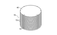
- the auxiliary drift electrode 70 may include a plurality of ring electrodes 72.
- the plurality of ring electrodes 72 are arranged along the facing direction.
- the ring electrode 72 includes a ring first surface 73 facing the drift electrode 40 and a ring second surface 74 located on the opposite side of the ring first surface 73.
- FIG. 30 is a plan view showing the ring electrode 72.
- An opening 721 is formed in the ring electrode 72.
- the opening 721 overlaps the electron detector 30 in the opposite direction.
- the ring electrode 72 does not have to overlap the electron detector 30 in the facing direction.
- the ring electrode 72 may overlap the drift electrode 40 in the facing direction.
- the ring electrode 72 has a width W1 in a plan view.
- the width W1 is, for example, 5 mm or more, may be 6 mm or more, or may be 8 mm or more.
- the width W1 is, for example, 30 mm or less, may be 25 mm or less, or may be 20 mm or less.
- the width W1 is the difference between the radius R11 of the circle forming the outer edge of the ring electrode 72 and the radius R12 of the circle forming the inner edge of the ring electrode 72.
- the ring electrode 72 may be composed of a wire having conductivity. For example, first, a wire having a first end and a second end is prepared. Subsequently, the wire is deformed into a circular shape or a polygonal shape to connect the first end and the second end. As a result, the ring electrode 72 is obtained.
- the width W1 of the ring electrode 72 corresponds to the dimension of the cross section of the wire. For example, if the cross section of the wire is circular, the width W1 of the ring electrode 72 is equal to the diameter of the cross section of the wire.
- the material of the wire is, for example, metal.
- the auxiliary drift electrode 70 may include a spacer 75 arranged between two adjacent ring electrodes 72 in the opposite direction.
- the spacer 75 determines the distance K5 between two adjacent ring electrodes 72 in the opposite direction.
- the distance K5 is determined according to the number of ring electrodes 72, the voltage between the electron detector 30 and the drift electrode 40, and the like.
- the distance K5 is, for example, 2 mm or more, may be 5 mm or more, or may be 8 mm or more.
- the distance K5 is, for example, 30 mm or less, may be 20 mm or less, or may be 15 mm or less.
- the drift electrode 40 may be attached to the auxiliary drift electrode 70.
- the auxiliary drift electrode 70 may include a spacer 75 located between the drift electrode 40 and the ring electrode 72.
- a structure including a drift electrode 40 and a plurality of ring electrodes 72 is also referred to as a drift cage 45.
- the auxiliary drift electrode 70 may include a wiring 76 that electrically connects two adjacent ring electrodes 72 in the opposite direction.
- the auxiliary drift electrode 70 may include a wiring 76 that electrically connects the adjacent drift electrode 40 and the ring electrode 72 in the facing direction.
- the auxiliary drift electrode 70 may include a resistor 77 inserted in the path of the wiring 76.
- the potential of the drift electrode 40 is -4000V
- the potential of the electron detector 30 is 0V
- 20 ring electrodes 72 are arranged between the drift electrode 40 and the electron detector 30.
- the potentials of the plurality of ring electrodes 72 arranged from the drift electrode 40 toward the electron detector 30 can be changed stepwise, such as -3800V, -3600V, -3400V, and so on. This makes it possible to improve the uniformity of the electric field formed in the space between the drift electrode 40 and the electron detector 30.
- the voltage between two adjacent ring electrodes 72 in the opposite direction is, for example, 50 V or more, 100 V or more, or 150 V or more.
- the voltage between two adjacent ring electrodes 72 in the opposite direction is, for example, 500 V or less, 400 V or less, or 300 V or less.
- the auxiliary drift electrode 70 may be supported by the relay board 90.
- the relay board 90 may support the electron detector 30.
- the relay board 90 may include a first board 91 that supports the electron detector 30, and a second board 92 that supports the auxiliary drift electrode 70.
- the second substrate 92 may be located between the first substrate 91 and the auxiliary drift electrode 70.
- the detection device 10 includes the electronic amplifier 60
- the electronic amplifier 60 may also be supported by the relay board 90.
- FIG. 31 is a cross-sectional view showing an example in which the auxiliary drift electrode 70 according to the second common modification is applied to the second embodiment.
- the radiation detector 50 may be located outside the container 20.
- the relay board 90 may be arranged on the second part 22.
- the relay board 90 may include a third board 93 extending from the inside of the container 20 to the outside.
- the relay board 90 may include a wire 95 that electrically connects the electron detector 30 and the first board 91.
- the electric signal of the electron detector 30 is transmitted to the outside of the container 20 via the wire 95, the first substrate 91 and the third substrate 93.
Abstract
Description
第1部と、第1方向において前記第1部に対向する第2部と、前記第1部から前記第2部に向かって広がる側部と、を含み、ガスが収容されている容器と、
前記容器の内部に位置し、コンプトン散乱によって発生した電子を検出する電子検出器と、
前記容器の内部において前記電子検出器よりも前記第2部の側に位置し、前記電子検出器に対向するドリフト電極と、
前記ドリフト電極よりも前記第2部の側に位置し、散乱された放射線を検出する放射線検出器と、を備える、検出装置である。 One embodiment of the present disclosure is a detection device that detects radiation.
A container containing a gas, including a first part, a second part facing the first part in the first direction, and a side part extending from the first part toward the second part.
An electron detector located inside the container to detect electrons generated by Compton scattering,
A drift electrode located inside the container on the side of the second part of the electron detector and facing the electron detector.
It is a detection device including a radiation detector that is located on the side of the second part of the drift electrode and detects scattered radiation.
第1部と、第1方向において前記第1部に対向する第2部と、前記第1部から前記第2部に向かって広がる側部と、を含み、ガスが収容されている容器と、
前記容器の内部に位置し、コンプトン散乱によって発生した電子を検出する電子検出器と、
前記容器の内部において前記電子検出器よりも前記第1部の側に位置し、前記電子検出器に対向するドリフト電極と、
前記電子検出器よりも前記第2部の側に位置し、散乱された放射線を検出する放射線検出器と、を備える、検出装置である。 One embodiment of the present disclosure is a detection device that detects radiation.
A container containing a gas, including a first part, a second part facing the first part in the first direction, and a side part extending from the first part toward the second part.
An electron detector located inside the container to detect electrons generated by Compton scattering,
A drift electrode located inside the container on the side of the first part of the electron detector and facing the electron detector.
It is a detection device including a radiation detector that is located on the side of the second part of the electron detector and detects scattered radiation.
第1部と、第1方向において前記第1部に対向する第2部と、前記第1部から前記第2部に向かって広がる側部と、を含み、ガスが収容されている容器と、
前記容器の内部に位置し、コンプトン散乱によって発生した電子を検出する電子検出器と、
前記容器の内部に位置し、前記第1方向に交差する方向において前記電子検出器に対向するドリフト電極と、
前記第1部よりも前記第2部に近接し、散乱された放射線を検出する放射線検出器と、を備える、検出装置である。 One embodiment of the present disclosure is a detection device that detects radiation.
A container containing a gas, including a first part, a second part facing the first part in the first direction, and a side part extending from the first part toward the second part.
An electron detector located inside the container to detect electrons generated by Compton scattering,
A drift electrode located inside the container and facing the electron detector in a direction intersecting the first direction,
It is a detection device including a radiation detector that is closer to the second part than the first part and detects scattered radiation.
前記電子増幅器は、表面及び裏面を含み、前記ドリフト電極と対向する方向において前記収集電極に重なる貫通孔が形成されている基材と、前記表面に位置する第1電極と、前記裏面に位置する第2電極と、を含んでいてもよい。 In the detector according to one embodiment of the present disclosure, the electron detector comprises a plurality of collection electrodes.
The electronic amplifier includes a front surface and a back surface, a base material having a through hole overlapping the collection electrode in a direction facing the drift electrode, a first electrode located on the front surface, and a first electrode located on the back surface. The second electrode may be included.
以下、本開示の第1の実施形態に係る検出装置10の構成について、図面を参照しながら詳細に説明する。まず、検出装置10の概要について説明する。図1は、検出装置10の一例を示す斜視図である。図2は、図1の検出装置10の断面図である。 First Embodiment Hereinafter, the configuration of the
検出装置10は、容器20と、容器20の内部に位置する電子検出器30、ドリフト電極40及び放射線検出器50と、を備える。容器20は、例えばチャンバーである。容器20の内部には、アルゴンやキセノンなどの希ガスが少なくとも収容されている。容器20の内部には、希ガスに加えて、二酸化炭素やメタンなどの消光作用を有するクエンチングガスが収容されていてもよい。 (Detection device)
The
例えば、検出素子51は、散乱された放射線によって励起されて蛍光を発するシンチレータと、蛍光を検出する光検出器と、を含んでいてもよい。光検出器は、例えばアバランシェフォトダイオードを含んでいてもよい。
検出素子51は、前記散乱された放射線を検出する半導体検出素子を含んでいてもよい。半導体検出素子は、例えば、テルル化亜鉛カドニウムを含む半導体を備えていてもよい。 The configuration of the
For example, the
The
次に、検出装置10の製造方法の一例を説明する。 (Manufacturing method of detector)
Next, an example of the manufacturing method of the
次に、図5を参照して、検出装置10の作用の一例を説明する。図5においては、容器20を省略している。 (Action of detector)
Next, an example of the operation of the
図6は、第1変形例に係る検出装置10を示す断面図である。検出装置10は、電子検出器30とドリフト電極40との間に位置する電子増幅器60を備えていてもよい。電子増幅器60は、例えば第1方向D1において電子検出器30及びドリフト電極40に対向するよう配置されている。 (First modification)
FIG. 6 is a cross-sectional view showing the
図7は、第2変形例に係る検出装置10を示す断面図である。検出装置10は、電子検出器30とドリフト電極40との間に位置する補助ドリフト電極70を備えていてもよい。補助ドリフト電極70は、電子検出器30とドリフト電極40とが対向する方向に広がる面71を含む。例えば、面71は第1方向D1に広がっている。 (Second modification)
FIG. 7 is a cross-sectional view showing the
図8は、第3変形例に係る検出装置10を示す断面図である。図8に示すように、放射線検出器50は、容器20の外部に位置していてもよい。例えば放射線検出器50は、第2部22の外側に位置していてもよい。放射線検出器50は、第2部22を挟んでドリフト電極40と対向していてもよい。 (Third modification example)
FIG. 8 is a cross-sectional view showing the
図9は、第4変形例に係る検出装置10を示す断面図である。検出装置10は、容器20の内部に位置する吸着材81を備えていてもよい。吸着材81は、容器20の内部に位置する電気部品から発生するアウトガスを吸着できる。例えば、吸着材81は、水蒸気、酸素などを吸着できる。吸着材81は、例えばチタンやジルコニウムなどの活性金属あるいは合金のゲッター材料、ゼオライトやシリカゲルなどの吸着材料、あるいはゲッターポンプなどである。 (Fourth modification)
FIG. 9 is a cross-sectional view showing the
図10は、第5変形例に係る検出装置10を示す断面図である。検出装置10は、容器20の内部に位置する電気部品から発生するアウトガスを除去するための装置を備えていてもよい。例えば、検出装置10は、容器20に接続されている循環路82と、循環路82に挿入されているポンプ83及びフィルタ84と、を備えていてもよい。 (Fifth modification)
FIG. 10 is a cross-sectional view showing the
図11は、第6変形例に係る検出装置10を示す断面図である。図11に示すように、ドリフト電極40は、複数の貫通孔41を含んでいてもよい。貫通孔41は、ドリフト電極40と放射線検出器50とが対向する方向において、例えば第1方向D1において、検出素子51と重なっていてもよい。 (6th modification)
FIG. 11 is a cross-sectional view showing the
次に、本開示の第2の実施の形態について説明する。第2の実施の形態において、第1の実施の形態と同一部分には同一符号を付して詳細な説明は省略する。また、第1の実施の形態において得られる作用効果が本実施の形態においても得られることが明らかである場合、その説明を省略することもある。 Second Embodiment Next, the second embodiment of the present disclosure will be described. In the second embodiment, the same parts as those in the first embodiment are designated by the same reference numerals, and detailed description thereof will be omitted. Further, when it is clear that the action and effect obtained in the first embodiment can be obtained in the present embodiment as well, the description thereof may be omitted.
次に、図14を参照して、検出装置10の作用の一例を説明する。図14においては、容器20を省略している。 (Action of detector)
Next, an example of the operation of the
次に、本開示の第3の実施の形態について説明する。第3の実施の形態において、第1の実施の形態と同一部分には同一符号を付して詳細な説明は省略する。また、第1の実施の形態において得られる作用効果が本実施の形態においても得られることが明らかである場合、その説明を省略することもある。 Third Embodiment Next, a third embodiment of the present disclosure will be described. In the third embodiment, the same parts as those in the first embodiment are designated by the same reference numerals, and detailed description thereof will be omitted. Further, when it is clear that the action and effect obtained in the first embodiment can be obtained in the present embodiment as well, the description thereof may be omitted.
次に、図17を参照して、検出装置10の作用の一例を説明する。図17においては、容器20を省略している。 (Action of detector)
Next, an example of the operation of the
図18は、第1変形例に係る検出装置10を示す断面図である。検出装置10は、電子検出器30とドリフト電極40との間に位置する電子増幅器60を備えていてもよい。電子増幅器60は、例えば第2方向D2において電子検出器30及びドリフト電極40に対向するよう配置されている。電子増幅器60を用いることにより、計測する電子の量が増える。このため、電子の位置などをより高い精度で検出できる。 (First modification)
FIG. 18 is a cross-sectional view showing the
図19は、第3変形例に係る検出装置10を示す断面図である。図19に示すように、放射線検出器50は、容器20の外部に位置していてもよい。例えば放射線検出器50は、第2部22の外側に位置していてもよい。放射線検出器50は、第2部22に対向していてもよい。 (Second modification)
FIG. 19 is a cross-sectional view showing the
第1の実施の形態の第2変形例の場合と同様に、検出装置10は、電子検出器30とドリフト電極40との間に位置する補助ドリフト電極70を備えていてもよい。第1の実施の形態の第4変形例の場合と同様に、検出装置10は、容器20の内部に位置する吸着材81を備えていてもよい。第1の実施の形態の第5変形例の場合と同様に、検出装置10は、容器20の内部に位置する電気部品から発生するアウトガスを除去するための装置を備えていてもよい。第1の実施の形態の第6変形例の場合と同様に、ドリフト電極40は、複数の貫通孔41を含んでいてもよい。 (Other variants)
As in the case of the second modification of the first embodiment, the
図21は、第1の共通変形例に係る容器20を示す斜視図である。図21に示すように、容器20は、第1部21及び側部23と、第1部21と側部23の間に位置するコーナー24と、を含んでいてもよい。第1部21は、平坦に広がっていてもよい。コーナー24は、第1部21及び側部23とは異なる方向に広がる面を含んでいてもよい。 (First common modification example)
FIG. 21 is a perspective view showing the
図28及び図29は、第2の共通変形例に係る補助ドリフト電極70を示す斜視図及び断面図である。補助ドリフト電極70は、複数のリング電極72を含んでいてもよい。複数のリング電極72は、対向方向に沿って並んでいる。リング電極72は、ドリフト電極40に向くリング第1面73と、リング第1面73の反対側に位置するリング第2面74と、を含む。 (Second common modification example)
28 and 29 are perspective views and cross-sectional views showing the
10 検出装置
20 容器
21 第1部
22 第2部
23 側部
24 コーナー
25 第1部分
26 第2部分
30 電子検出器
31 収集電極
32 支持基板
40 ドリフト電極
41 貫通孔
45 ドリフトケージ
50 放射線検出器
51 検出素子
52 回路基板
60 電子増幅器
61 第1電極
62 第2電極
63 基材
64 貫通孔
70 補助ドリフト電極
72 リング電極
73 リング第1面
74 リング第2面
75 スペーサ
76 配線
77 抵抗器
81 吸着材
82 循環路
83 ポンプ
84 フィルタ
90 中継基板
91 第1基板
92 第2基板
93 第3基板
95 ワイヤ 5
Claims (23)
- 放射線を検出する検出装置であって、
第1部と、第1方向において前記第1部に対向する第2部と、前記第1部から前記第2部に向かって広がる側部と、を含み、ガスが収容されている容器と、
前記容器の内部に位置し、コンプトン散乱によって発生した電子を検出する電子検出器と、
前記容器の内部において前記電子検出器よりも前記第2部の側に位置し、前記電子検出器に対向するドリフト電極と、
前記ドリフト電極よりも前記第2部の側に位置し、散乱された放射線を検出する放射線検出器と、を備える、検出装置。 A detector that detects radiation
A container containing a gas, including a first part, a second part facing the first part in the first direction, and a side part extending from the first part toward the second part.
An electron detector located inside the container to detect electrons generated by Compton scattering,
A drift electrode located inside the container on the side of the second part of the electron detector and facing the electron detector.
A detection device including a radiation detector that is located on the side of the second part of the drift electrode and detects scattered radiation. - 前記放射線検出器は、前記容器の内部に位置している、請求項1に記載の検出装置。 The detection device according to claim 1, wherein the radiation detector is located inside the container.
- 前記放射線検出器は、前記容器の外部に位置している、請求項1に記載の検出装置。 The detection device according to claim 1, wherein the radiation detector is located outside the container.
- 前記第1部は、前記電子検出器と前記ドリフト電極とが対向する方向に沿って見た場合に前記電子検出器に重なる範囲において平坦に広がる外面を含む、請求項1乃至3のいずれか一項に記載の検出装置。 One of claims 1 to 3, wherein the first part includes an outer surface that spreads flat in a range overlapping the electron detector when viewed along a direction in which the electron detector and the drift electrode face each other. The detector described in the section.
- 前記第1部の内面と前記電子検出器との間の距離が、10mm以下である、請求項4に記載の検出装置。 The detection device according to claim 4, wherein the distance between the inner surface of the first part and the electronic detector is 10 mm or less.
- 放射線を検出する検出装置であって、
第1部と、第1方向において前記第1部に対向する第2部と、前記第1部から前記第2部に向かって広がる側部と、を含み、ガスが収容されている容器と、
前記容器の内部に位置し、コンプトン散乱によって発生した電子を検出する電子検出器と、
前記容器の内部において前記電子検出器よりも前記第1部の側に位置し、前記電子検出器に対向するドリフト電極と、
前記電子検出器よりも前記第2部の側に位置し、散乱された放射線を検出する放射線検出器と、を備える、検出装置。 A detector that detects radiation
A container containing a gas, including a first part, a second part facing the first part in the first direction, and a side part extending from the first part toward the second part.
An electron detector located inside the container to detect electrons generated by Compton scattering,
A drift electrode located inside the container on the side of the first part of the electron detector and facing the electron detector.
A detection device including a radiation detector that is located on the side of the second part of the electron detector and detects scattered radiation. - 前記放射線検出器は、前記容器の内部に位置している、請求項6に記載の検出装置。 The detection device according to claim 6, wherein the radiation detector is located inside the container.
- 前記放射線検出器は、前記容器の外部に位置している、請求項6に記載の検出装置。 The detection device according to claim 6, wherein the radiation detector is located outside the container.
- 前記第1部は、前記電子検出器と前記ドリフト電極とが対向する方向に沿って見た場合に前記ドリフト電極に重なる範囲において平坦に広がる外面を含む、請求項6乃至8のいずれか一項に記載の検出装置。 One of claims 6 to 8, wherein the first part includes an outer surface that spreads flat in a range overlapping the drift electrode when viewed along a direction in which the electron detector and the drift electrode face each other. The detector according to.
- 前記第1部の内面と前記ドリフト電極との間の距離が、10mm以上100mm以下である、請求項9に記載の検出装置。 The detection device according to claim 9, wherein the distance between the inner surface of the first part and the drift electrode is 10 mm or more and 100 mm or less.
- 前記ドリフト電極は、複数の貫通孔を含む、請求項1乃至10のいずれか一項に記載の検出装置。 The detection device according to any one of claims 1 to 10, wherein the drift electrode includes a plurality of through holes.
- 放射線を検出する検出装置であって、
第1部と、第1方向において前記第1部に対向する第2部と、前記第1部から前記第2部に向かって広がる側部と、を含み、ガスが収容されている容器と、
前記容器の内部に位置し、コンプトン散乱によって発生した電子を検出する電子検出器と、
前記容器の内部に位置し、前記第1方向に交差する方向において前記電子検出器に対向するドリフト電極と、
前記第1部よりも前記第2部に近接し、散乱された放射線を検出する放射線検出器と、を備える、検出装置。 A detector that detects radiation
A container containing a gas, including a first part, a second part facing the first part in the first direction, and a side part extending from the first part toward the second part.
An electron detector located inside the container to detect electrons generated by Compton scattering,
A drift electrode located inside the container and facing the electron detector in a direction intersecting the first direction,
A detection device including a radiation detector that is closer to the second part than the first part and detects scattered radiation. - 前記放射線検出器は、前記容器の内部に位置している、請求項12に記載の検出装置。 The detection device according to claim 12, wherein the radiation detector is located inside the container.
- 前記放射線検出器は、前記容器の外部に位置している、請求項12に記載の検出装置。 The detection device according to claim 12, wherein the radiation detector is located outside the container.
- 前記電子検出器と前記ドリフト電極との間に位置し、前記電子検出器及び前記ドリフト電極に対向する電子増幅器を備える、請求項1乃至14のいずれか一項に記載の検出装置。 The detection device according to any one of claims 1 to 14, which is located between the electron detector and the drift electrode and includes the electron detector and an electronic amplifier facing the drift electrode.
- 前記電子検出器は、複数の収集電極を含み、
前記電子増幅器は、表面及び裏面を含み、前記ドリフト電極と対向する方向において前記収集電極に重なる貫通孔が形成されている基材と、前記表面に位置する第1電極と、前記裏面に位置する第2電極と、を含む、請求項15に記載の検出装置。 The electron detector includes a plurality of collection electrodes.
The electronic amplifier includes a front surface and a back surface, a base material having a through hole overlapping the collection electrode in a direction facing the drift electrode, a first electrode located on the front surface, and a first electrode located on the back surface. The detection device according to claim 15, comprising a second electrode. - 前記電子検出器と前記ドリフト電極とが対向する方向に沿って並ぶ複数のリング電極と、隣り合う2つの前記リング電極の間に位置するスペーサと、を含む補助ドリフト電極を備える、請求項1乃至16のいずれか一項に記載の検出装置。 1 to claim 1, further comprising an auxiliary drift electrode including a plurality of ring electrodes arranged along a direction in which the electron detector and the drift electrode face each other, and a spacer located between two adjacent ring electrodes. 16. The detection device according to any one of 16.
- 前記電子検出器と前記ドリフト電極とが対向する方向に沿って並ぶ複数のリング電極と、隣り合う2つの前記リング電極の間に位置するスペーサと、を含む補助ドリフト電極と、
前記補助ドリフト電極及び前記電子検出器を支持する中継基板と、を備え、
前記ドリフト電極は、前記電子検出器と対向するよう前記補助ドリフト電極に取り付けられており、
前記中継基板は、前記第2部上に配置されている、請求項8に記載の検出装置。 An auxiliary drift electrode including a plurality of ring electrodes arranged along a direction in which the electron detector and the drift electrode face each other, and a spacer located between two adjacent ring electrodes.
The auxiliary drift electrode and the relay board supporting the electron detector are provided.
The drift electrode is attached to the auxiliary drift electrode so as to face the electron detector.
The detection device according to claim 8, wherein the relay board is arranged on the second part. - 前記放射線検出器は、前記散乱された放射線によって励起されて蛍光を発するシンチレータと、前記蛍光を検出する光検出器と、を含む、請求項1乃至18のいずれか一項に記載の検出装置。 The detection device according to any one of claims 1 to 18, wherein the radiation detector includes a scintillator that is excited by the scattered radiation to emit fluorescence, and a photodetector that detects the fluorescence.
- 前記放射線検出器は、前記散乱された放射線を検出する半導体検出素子を含む、請求項1乃至19のいずれか一項に記載の検出装置。 The detection device according to any one of claims 1 to 19, wherein the radiation detector includes a semiconductor detection element that detects the scattered radiation.
- 前記容器の側部は円筒形を有する、請求項1乃至20のいずれか一項に記載の検出装置。 The detection device according to any one of claims 1 to 20, wherein the side portion of the container has a cylindrical shape.
- 前記容器の内部に位置する吸着材を備える、請求項1乃至21のいずれか一項に記載の検出装置。 The detection device according to any one of claims 1 to 21, comprising an adsorbent located inside the container.
- 前記容器に接続されている循環路と、前記循環路に挿入されているポンプ及びフィルタと、を備える、請求項1乃至22のいずれか一項に記載の検出装置。 The detection device according to any one of claims 1 to 22, comprising a circulation path connected to the container and a pump and a filter inserted in the circulation path.
Priority Applications (6)
| Application Number | Priority Date | Filing Date | Title |
|---|---|---|---|
| CN202180067162.5A CN116324518A (en) | 2020-10-01 | 2021-09-30 | Detection device |
| EP21875845.6A EP4224216A1 (en) | 2020-10-01 | 2021-09-30 | Detection device |
| JP2022515131A JP7215639B2 (en) | 2020-10-01 | 2021-09-30 | detector |
| US18/029,771 US20230384465A1 (en) | 2020-10-01 | 2021-09-30 | Detection device |
| JP2022198252A JP7420208B2 (en) | 2020-10-01 | 2022-12-12 | detection device |
| JP2024002108A JP2024038315A (en) | 2020-10-01 | 2024-01-10 | detection device |
Applications Claiming Priority (2)
| Application Number | Priority Date | Filing Date | Title |
|---|---|---|---|
| JP2020167130 | 2020-10-01 | ||
| JP2020-167130 | 2020-10-01 |
Publications (1)
| Publication Number | Publication Date |
|---|---|
| WO2022071549A1 true WO2022071549A1 (en) | 2022-04-07 |
Family
ID=80950551
Family Applications (1)
| Application Number | Title | Priority Date | Filing Date |
|---|---|---|---|
| PCT/JP2021/036348 WO2022071549A1 (en) | 2020-10-01 | 2021-09-30 | Detection device |
Country Status (5)
| Country | Link |
|---|---|
| US (1) | US20230384465A1 (en) |
| EP (1) | EP4224216A1 (en) |
| JP (3) | JP7215639B2 (en) |
| CN (1) | CN116324518A (en) |
| WO (1) | WO2022071549A1 (en) |
Cited By (1)
| Publication number | Priority date | Publication date | Assignee | Title |
|---|---|---|---|---|
| WO2024048759A1 (en) * | 2022-08-31 | 2024-03-07 | 大日本印刷株式会社 | Detection device and radiation identification device |
Families Citing this family (1)
| Publication number | Priority date | Publication date | Assignee | Title |
|---|---|---|---|---|
| EP4224216A1 (en) * | 2020-10-01 | 2023-08-09 | Dai Nippon Printing Co., Ltd. | Detection device |
Citations (9)
| Publication number | Priority date | Publication date | Assignee | Title |
|---|---|---|---|---|
| JP2003536079A (en) * | 2000-06-05 | 2003-12-02 | エックスカウンター アーベー | Radiation detection device and method |
| JP2004020249A (en) * | 2002-06-13 | 2004-01-22 | Toshiba Corp | Radiation detecting instrument |
| JP2007520865A (en) * | 2004-02-03 | 2007-07-26 | オルガニゼイション ユーロピエンヌ プール ラ レシェルシェ ニュークリエル | Radiation detector |
| JP2007234485A (en) * | 2006-03-02 | 2007-09-13 | Institute Of Physical & Chemical Research | Gas electron multiplier, manufacturing method of gas electron multiplication foil using it, and radiation detector using gas electron multiplier |
| JP2015190965A (en) * | 2014-03-28 | 2015-11-02 | キヤノン株式会社 | Radiation measuring device and radiation measuring method |
| JP2016161522A (en) | 2015-03-05 | 2016-09-05 | キヤノン株式会社 | Radiation detection device and compton camera |
| JP2016217874A (en) | 2015-05-20 | 2016-12-22 | キヤノン株式会社 | Ionizing radiation detector |
| WO2017057674A1 (en) | 2015-09-30 | 2017-04-06 | 大日本印刷株式会社 | Radiation image forming device |
| JP2021043081A (en) * | 2019-09-11 | 2021-03-18 | 株式会社日立製作所 | Gamma ray measurer, particle beam irradiation system, and measurement method |
Family Cites Families (10)
| Publication number | Priority date | Publication date | Assignee | Title |
|---|---|---|---|---|
| FI112285B (en) | 2001-12-20 | 2003-11-14 | Ari Virtanen | Method and apparatus for determining the intensity distribution of a time-dependent radiation field |
| JP5152950B2 (en) | 2005-07-29 | 2013-02-27 | 独立行政法人科学技術振興機構 | Microchannel plate, gas proportional counter, and imaging device |
| WO2008099921A1 (en) | 2007-02-16 | 2008-08-21 | Inter-University Research Institute Corporation High Energy Accelerator Research Organization | Gamma ray detector and pet device employing the same |
| JP2010286316A (en) | 2009-06-10 | 2010-12-24 | Univ Of Tokyo | Optical detector |
| JP2017096724A (en) | 2015-11-20 | 2017-06-01 | キヤノン株式会社 | Radiation detector |
| FR3051258B1 (en) | 2016-05-11 | 2019-08-02 | Centre National De La Recherche Scientifique | METHOD AND DEVICE FOR DETERMINING THE DENSITY OF ROCKY VOLUMES OR ARTIFICIAL BUILDINGS |
| JP6860369B2 (en) | 2017-02-09 | 2021-04-14 | 浜松ホトニクス株式会社 | Proportional counter and neutron imaging system |
| US10134571B1 (en) | 2018-01-26 | 2018-11-20 | C-Rad Imaging Ab | Detector for incident radiation |
| EP3770639A4 (en) | 2018-03-19 | 2021-04-14 | FUJIFILM Corporation | Radiation detector, radiographic photography device, and production method for radiation detector |
| EP4224216A1 (en) | 2020-10-01 | 2023-08-09 | Dai Nippon Printing Co., Ltd. | Detection device |
-
2021
- 2021-09-30 EP EP21875845.6A patent/EP4224216A1/en active Pending
- 2021-09-30 WO PCT/JP2021/036348 patent/WO2022071549A1/en active Application Filing
- 2021-09-30 CN CN202180067162.5A patent/CN116324518A/en active Pending
- 2021-09-30 US US18/029,771 patent/US20230384465A1/en active Pending
- 2021-09-30 JP JP2022515131A patent/JP7215639B2/en active Active
-
2022
- 2022-12-12 JP JP2022198252A patent/JP7420208B2/en active Active
-
2024
- 2024-01-10 JP JP2024002108A patent/JP2024038315A/en active Pending
Patent Citations (9)
| Publication number | Priority date | Publication date | Assignee | Title |
|---|---|---|---|---|
| JP2003536079A (en) * | 2000-06-05 | 2003-12-02 | エックスカウンター アーベー | Radiation detection device and method |
| JP2004020249A (en) * | 2002-06-13 | 2004-01-22 | Toshiba Corp | Radiation detecting instrument |
| JP2007520865A (en) * | 2004-02-03 | 2007-07-26 | オルガニゼイション ユーロピエンヌ プール ラ レシェルシェ ニュークリエル | Radiation detector |
| JP2007234485A (en) * | 2006-03-02 | 2007-09-13 | Institute Of Physical & Chemical Research | Gas electron multiplier, manufacturing method of gas electron multiplication foil using it, and radiation detector using gas electron multiplier |
| JP2015190965A (en) * | 2014-03-28 | 2015-11-02 | キヤノン株式会社 | Radiation measuring device and radiation measuring method |
| JP2016161522A (en) | 2015-03-05 | 2016-09-05 | キヤノン株式会社 | Radiation detection device and compton camera |
| JP2016217874A (en) | 2015-05-20 | 2016-12-22 | キヤノン株式会社 | Ionizing radiation detector |
| WO2017057674A1 (en) | 2015-09-30 | 2017-04-06 | 大日本印刷株式会社 | Radiation image forming device |
| JP2021043081A (en) * | 2019-09-11 | 2021-03-18 | 株式会社日立製作所 | Gamma ray measurer, particle beam irradiation system, and measurement method |
Cited By (1)
| Publication number | Priority date | Publication date | Assignee | Title |
|---|---|---|---|---|
| WO2024048759A1 (en) * | 2022-08-31 | 2024-03-07 | 大日本印刷株式会社 | Detection device and radiation identification device |
Also Published As
| Publication number | Publication date |
|---|---|
| JP7420208B2 (en) | 2024-01-23 |
| JP2023025252A (en) | 2023-02-21 |
| JPWO2022071549A1 (en) | 2022-04-07 |
| EP4224216A1 (en) | 2023-08-09 |
| US20230384465A1 (en) | 2023-11-30 |
| JP7215639B2 (en) | 2023-01-31 |
| JP2024038315A (en) | 2024-03-19 |
| CN116324518A (en) | 2023-06-23 |
Similar Documents
| Publication | Publication Date | Title |
|---|---|---|
| JP7420208B2 (en) | detection device | |
| JP4931793B2 (en) | Mass spectrometer focal plane detector assembly | |
| US8853643B2 (en) | Protected readout electrode assembly | |
| JP4613319B2 (en) | Gas radiation detector | |
| AU4442700A (en) | A method for detecting ionizing radiation, a radiation detector and an apparatusfor use in planar beam radiography | |
| JP2023036732A (en) | Silicon drift type radiation detection element, silicon drift type radiation detector and radiation detection device | |
| JP5604751B2 (en) | Particle beam image detector with pixel electrode using high resistance electrode | |
| JPS5831551B2 (en) | X-ray detector | |
| JP2016024085A (en) | Silicon drift detector | |
| JP6041484B2 (en) | Neutron detector | |
| US11346806B2 (en) | Low profile ionization detector | |
| JP2007139479A (en) | Nuclear medical diagnostic system and nuclear medical diagnostic method | |
| ES2751332T3 (en) | A wallless electron multiplier set | |
| JP2009206057A (en) | Gas electron amplifier and radiation detector using the same | |
| JP2009222410A (en) | Radiation detector | |
| JP4671153B2 (en) | Open window ionization chamber | |
| JP2005005128A (en) | Ion mobility detector | |
| JP2013191428A (en) | Electronic tube | |
| US7639783B1 (en) | Parallax free and spark protected X-ray detector | |
| JP5371057B2 (en) | Ionization gauge | |
| KR100860484B1 (en) | Large-area, multi-segmented, two-dimensional, position-sensitive proportional, gas injection type counter | |
| JPS5831877B2 (en) | X-ray detector | |
| JP2013044732A (en) | Detector | |
| JP2008027795A (en) | Proportional counter tube | |
| RU2398309C1 (en) | Drift tube structure for ion mobility spectrometre |
Legal Events
| Date | Code | Title | Description |
|---|---|---|---|
| ENP | Entry into the national phase |
Ref document number: 2022515131 Country of ref document: JP Kind code of ref document: A |
|
| 121 | Ep: the epo has been informed by wipo that ep was designated in this application |
Ref document number: 21875845 Country of ref document: EP Kind code of ref document: A1 |
|
| WWE | Wipo information: entry into national phase |
Ref document number: 18029771 Country of ref document: US |
|
| NENP | Non-entry into the national phase |
Ref country code: DE |
|
| ENP | Entry into the national phase |
Ref document number: 2021875845 Country of ref document: EP Effective date: 20230502 |