JP4931793B2 - Mass spectrometer focal plane detector assembly - Google Patents
Mass spectrometer focal plane detector assembly Download PDFInfo
- Publication number
- JP4931793B2 JP4931793B2 JP2007502023A JP2007502023A JP4931793B2 JP 4931793 B2 JP4931793 B2 JP 4931793B2 JP 2007502023 A JP2007502023 A JP 2007502023A JP 2007502023 A JP2007502023 A JP 2007502023A JP 4931793 B2 JP4931793 B2 JP 4931793B2
- Authority
- JP
- Japan
- Prior art keywords
- assembly
- microchannel plate
- electron multiplier
- mass spectrometer
- plate electron
- Prior art date
- Legal status (The legal status is an assumption and is not a legal conclusion. Google has not performed a legal analysis and makes no representation as to the accuracy of the status listed.)
- Active
Links
- 150000002500 ions Chemical class 0.000 claims description 77
- 238000000034 method Methods 0.000 claims description 9
- 230000005684 electric field Effects 0.000 claims description 8
- 239000012212 insulator Substances 0.000 claims description 6
- 238000005452 bending Methods 0.000 claims 1
- 238000001514 detection method Methods 0.000 description 7
- 230000003287 optical effect Effects 0.000 description 6
- 238000005259 measurement Methods 0.000 description 5
- 230000008569 process Effects 0.000 description 5
- 238000000926 separation method Methods 0.000 description 5
- 239000012855 volatile organic compound Substances 0.000 description 5
- 238000011161 development Methods 0.000 description 4
- 230000018109 developmental process Effects 0.000 description 4
- 238000010884 ion-beam technique Methods 0.000 description 4
- 239000004065 semiconductor Substances 0.000 description 4
- 238000004458 analytical method Methods 0.000 description 3
- 238000010586 diagram Methods 0.000 description 3
- 238000005516 engineering process Methods 0.000 description 3
- 238000001819 mass spectrum Methods 0.000 description 3
- 239000002245 particle Substances 0.000 description 3
- 125000006850 spacer group Chemical group 0.000 description 3
- 230000008901 benefit Effects 0.000 description 2
- 238000006243 chemical reaction Methods 0.000 description 2
- 238000000708 deep reactive-ion etching Methods 0.000 description 2
- 230000009977 dual effect Effects 0.000 description 2
- 238000010849 ion bombardment Methods 0.000 description 2
- 238000004949 mass spectrometry Methods 0.000 description 2
- 230000015654 memory Effects 0.000 description 2
- 238000012986 modification Methods 0.000 description 2
- 230000004048 modification Effects 0.000 description 2
- 239000013307 optical fiber Substances 0.000 description 2
- 239000000758 substrate Substances 0.000 description 2
- OAICVXFJPJFONN-UHFFFAOYSA-N Phosphorus Chemical compound [P] OAICVXFJPJFONN-UHFFFAOYSA-N 0.000 description 1
- XUIMIQQOPSSXEZ-UHFFFAOYSA-N Silicon Chemical compound [Si] XUIMIQQOPSSXEZ-UHFFFAOYSA-N 0.000 description 1
- 238000013459 approach Methods 0.000 description 1
- 238000000429 assembly Methods 0.000 description 1
- 230000000712 assembly Effects 0.000 description 1
- 230000015572 biosynthetic process Effects 0.000 description 1
- 230000000903 blocking effect Effects 0.000 description 1
- 238000000451 chemical ionisation Methods 0.000 description 1
- 238000007796 conventional method Methods 0.000 description 1
- BHEPBYXIRTUNPN-UHFFFAOYSA-N hydridophosphorus(.) (triplet) Chemical compound [PH] BHEPBYXIRTUNPN-UHFFFAOYSA-N 0.000 description 1
- 238000003698 laser cutting Methods 0.000 description 1
- 238000004519 manufacturing process Methods 0.000 description 1
- 239000000463 material Substances 0.000 description 1
- 229910052751 metal Inorganic materials 0.000 description 1
- 239000002184 metal Substances 0.000 description 1
- 229910044991 metal oxide Inorganic materials 0.000 description 1
- 150000004706 metal oxides Chemical class 0.000 description 1
- 239000000203 mixture Substances 0.000 description 1
- 238000012544 monitoring process Methods 0.000 description 1
- 230000009467 reduction Effects 0.000 description 1
- 230000004044 response Effects 0.000 description 1
- 229910052702 rhenium Inorganic materials 0.000 description 1
- WUAPFZMCVAUBPE-UHFFFAOYSA-N rhenium atom Chemical compound [Re] WUAPFZMCVAUBPE-UHFFFAOYSA-N 0.000 description 1
- 230000035945 sensitivity Effects 0.000 description 1
- 229910052710 silicon Inorganic materials 0.000 description 1
- 239000010703 silicon Substances 0.000 description 1
- 238000001228 spectrum Methods 0.000 description 1
- 238000007740 vapor deposition Methods 0.000 description 1
- 239000011364 vaporized material Substances 0.000 description 1
Images


Classifications
-
- H—ELECTRICITY
- H01—ELECTRIC ELEMENTS
- H01J—ELECTRIC DISCHARGE TUBES OR DISCHARGE LAMPS
- H01J49/00—Particle spectrometers or separator tubes
- H01J49/02—Details
- H01J49/04—Arrangements for introducing or extracting samples to be analysed, e.g. vacuum locks; Arrangements for external adjustment of electron- or ion-optical components
-
- G—PHYSICS
- G01—MEASURING; TESTING
- G01N—INVESTIGATING OR ANALYSING MATERIALS BY DETERMINING THEIR CHEMICAL OR PHYSICAL PROPERTIES
- G01N30/00—Investigating or analysing materials by separation into components using adsorption, absorption or similar phenomena or using ion-exchange, e.g. chromatography or field flow fractionation
- G01N30/02—Column chromatography
- G01N30/62—Detectors specially adapted therefor
- G01N30/72—Mass spectrometers
- G01N30/7206—Mass spectrometers interfaced to gas chromatograph
-
- H—ELECTRICITY
- H01—ELECTRIC ELEMENTS
- H01J—ELECTRIC DISCHARGE TUBES OR DISCHARGE LAMPS
- H01J49/00—Particle spectrometers or separator tubes
- H01J49/02—Details
- H01J49/025—Detectors specially adapted to particle spectrometers
-
- H—ELECTRICITY
- H01—ELECTRIC ELEMENTS
- H01J—ELECTRIC DISCHARGE TUBES OR DISCHARGE LAMPS
- H01J49/00—Particle spectrometers or separator tubes
- H01J49/26—Mass spectrometers or separator tubes
- H01J49/28—Static spectrometers
- H01J49/32—Static spectrometers using double focusing
- H01J49/322—Static spectrometers using double focusing with a magnetic sector of 90 degrees, e.g. Mattauch-Herzog type
-
- H—ELECTRICITY
- H01—ELECTRIC ELEMENTS
- H01J—ELECTRIC DISCHARGE TUBES OR DISCHARGE LAMPS
- H01J49/00—Particle spectrometers or separator tubes
- H01J49/44—Energy spectrometers, e.g. alpha-, beta-spectrometers
- H01J49/46—Static spectrometers
- H01J49/48—Static spectrometers using electrostatic analysers, e.g. cylindrical sector, Wien filter
Description
(関連出願への相互参照)
本出願は、2004年3月31日に出願された米国仮特許出願第60/577,920号;2004年3月31日に出願された米国仮特許出願第60/557,969号;2004年3月5日に出願された米国仮特許出願第60/550,663号;および2004年3月5日に出願された米国仮特許出願第60/550,664号の利益を主張し、ここで、これら4つの仮出願は、それらの全体が参考として本明細書中に援用される。
(Cross-reference to related applications)
This application is based on US Provisional Patent Application No. 60 / 577,920 filed on March 31, 2004; US Provisional Patent Application No. 60 / 557,969 filed on March 31, 2004; 2004 Claims the benefit of US Provisional Patent Application No. 60 / 550,663, filed Mar. 5, and US Provisional Patent Application No. 60 / 550,664, filed Mar. 5, 2004, where These four provisional applications are hereby incorporated by reference in their entirety.
(発明の背景)
(発明の分野)
本発明は、一般に質量分析計の分野に、そして特にその焦点面検出器に関する。
(Background of the Invention)
(Field of Invention)
The present invention relates generally to the field of mass spectrometers, and more particularly to its focal plane detector.
(関連する技術の説明)
質量分析計は、プロセスモニタリングから生命科学まで多くの適用で広く用いられている。過去60年間の経過に亘って種々の器具が開発されてきた。新たな開発の焦点は、2つの部分からなる:(1)高質量解像度とともになお高い質量範囲のための懸命の努力、および(2)小さな、デスクトップ質量分析計器具の開発に関する。
(Description of related technology)
Mass spectrometers are widely used in many applications from process monitoring to life sciences. Various instruments have been developed over the past 60 years. The new development focus consists of two parts: (1) hard efforts for still high mass ranges with high mass resolution, and (2) development of small, desktop mass spectrometer instruments.
質量分析計は、しばしば、複雑な混合物の分析のためにガスクロマトグラフと組み合わされる。これは、特に、揮発性有機化合物(VOC)および準揮発性有機化合物(semi−VOC)の分析のために有用である。組み合わされたガスクロマトグラフおよび質量分析計または分光器(GS/MS)器具は、代表的には、ガス入口システムを含み、これは、GC/MS器具のガスクロマトグラフ部分を含み得る。このGC/MS器具はまた、代表的には、イオン抽出器を備えた、電子衝撃(EI)を基礎にしたイオナイザー、イオンビームを焦点集めするためのイオン光学(optic)構成要素、イオン分離構成要素、およびイオン検出構成要素を含む。イオン化はまた、化学的イオン化を経由して実施され得る。 Mass spectrometers are often combined with gas chromatographs for the analysis of complex mixtures. This is particularly useful for the analysis of volatile organic compounds (VOC) and semi-volatile organic compounds (semi-VOC). A combined gas chromatograph and mass spectrometer or spectrometer (GS / MS) instrument typically includes a gas inlet system, which may include the gas chromatograph portion of the GC / MS instrument. The GC / MS instrument also typically includes an ion bombardment ionizer (EI) ionizer with an ion extractor, an ion optics component for focusing the ion beam, an ion separation configuration. Element, and an ion detection component. Ionization can also be performed via chemical ionization.
イオン分離は、時間または空間ドメインで実施され得る。時間ドメインにおける質量分離の例は、飛行時間型質量分析計である。空間的分離は、一般に用いられる四重極質量分析計で観察される。ここで、「四重極フィルター」は、イオナイザーから検出器に伝達される唯一の質量/電荷比を可能にする。完全な質量スペクトルは、この「質量フィルター」を通る質量範囲を走査することにより記録される。その他の空間的分離は、イオンエネルギーまたは磁場強度いずれかが変動される磁場に基づき、ここで再び、上記質量フィルターは、伝達されるべき唯一の質量/電荷比を可能にし、そしてスペクトルは、この質量範囲を通じて走査することにより記録され得る。 Ion separation can be performed in the time or space domain. An example of mass separation in the time domain is a time-of-flight mass spectrometer. Spatial separation is observed with commonly used quadrupole mass spectrometers. Here, a “quadrupole filter” allows for the only mass / charge ratio transferred from the ionizer to the detector. A complete mass spectrum is recorded by scanning the mass range through this “mass filter”. Other spatial separations are based on magnetic fields in which either ion energy or magnetic field strength is varied, where again the mass filter allows only one mass / charge ratio to be transmitted and the spectrum is It can be recorded by scanning through the mass range.
質量分析計の1つのタイプは質量分光器である。質量分光器においては、イオンは、磁場で空間的に分離され、そして位置感受性検出器で検出される。二重焦点合わせ質量分析計の概念は、最初、MattauchおよびHerzog(MH)によって1940年に導入された(非特許文献1)。 One type of mass spectrometer is a mass spectrometer. In a mass spectrometer, ions are spatially separated with a magnetic field and detected with a position sensitive detector. The concept of a double focusing mass spectrometer was first introduced in 1940 by Mattauch and Herzog (MH) (1).
二重焦点合わせは、拡散されたエネルギーおよび拡散された空間的ビームの両方を再焦点合わせする器具の能力をいう。磁石およびマイクロマシン技術における現代の発展は、これら器具のサイズにおける劇的な減少を可能にする。VOCおよび準VOC分析を行い得る質量分析計における焦点面の長さは、数センチメートルまで低減されている。 Double focusing refers to the ability of the instrument to refocus both the diffused energy and the diffused spatial beam. Modern developments in magnet and micromachine technology allow for dramatic reductions in the size of these instruments. The length of the focal plane in a mass spectrometer capable of performing VOC and quasi-VOC analysis has been reduced to a few centimeters.
小共焦点面レイアウトMattauch−Herzog器具の代表的な仕様は、以下のように要約される:
電子衝撃イオン化、レニウムフィラメント
DC−電圧および永久磁石
イオンエネルギー:0.5−2.5kV DC
質量範囲:2−200D
ファラデーカップ検出器アレイまたはストリップ電荷検出器
10∧11までのゲインを備えた積算操作性増幅器
衝撃係数(デューティサイクル):>99%
読み出し時間:0.03秒〜10秒
感度:ストリップ電荷検出器で約10ppm
さらに、イオン光学要素は、減圧チャンバーフロア内またはチャンバー壁上に取り付けられる。これらの光学要素はまた、減圧ハウジングの一体部分であり得る。小器具では、しかし、これらイオン光学要素は、「光学ベンチ」として作用するベースプレート上に構築され得る。このベンチは、これらイオン光学要素を支持する。このベースプレートは、減圧またはマスターフランジに対して取り付けられ、減圧下で質量分析計を作動するために必要な減圧シールを提供する。上記ベースプレートはまた、それ自体、減圧またはマスターフランジとして作用し得る。
Typical specifications for a small confocal plane layout Mattauch-Herzog instrument are summarized as follows:
Electron impact ionization, rhenium filament DC-voltage and permanent magnet ion energy: 0.5-2.5 kV DC
Mass range: 2-200D
Integrated Operative Amplifier Impact Factor (Duty Cycle) with Gain up to Faraday Cup Detector Array or
Readout time: 0.03 seconds to 10 seconds Sensitivity: about 10 ppm with strip charge detector
Furthermore, the ion optical element is mounted in the vacuum chamber floor or on the chamber wall. These optical elements can also be an integral part of the vacuum housing. In an instrument, however, these ion optical elements can be built on a base plate that acts as an “optical bench”. This bench supports these ion optical elements. This base plate is attached to a vacuum or a master flange and provides the vacuum seal necessary to operate the mass spectrometer under vacuum. The base plate can also itself act as a vacuum or a master flange.
Mattauch−Herzogイオン検出器は、位置感受性検出器である。多くの概念が、過去十年間に亘って開発されてきた。最近の開発は、従前に用いられた電子光学イオン検出(EOID)の代替として半導体ベースの直接イオン検出に焦点をあてている。 The Mattauch-Herzog ion detector is a position sensitive detector. Many concepts have been developed over the past decade. Recent developments have focused on semiconductor-based direct ion detection as an alternative to the previously used electron optical ion detection (EOID).
この電子光学イオン検出(EOID)は、マルチチャネルプレート(MCP)中のイオンを、電子に変換し、(同じMCP中の)これら電子を増幅し、そしてこのMCPから発せられる電子で衝突されるリンのフィルムを照射する。リンのフィルム上に形成されたイメージは、光ファイバーカプラーを経由して発光ダイオードアレイで記録される。このタイプのEOIDは、特許文献1に詳細に記載されている。このEOIDは、質量分析計の焦点面に沿って空間的に分離されたイオンの同時測定のために意図されている。このEOIDは、イオンを電子に、そして次に光子に転換することによって作動される。これら光子は、イオン誘導信号のイメージを形成する。これらイオンは、マイクロチャネル電子電子増倍管アレイに衝突することにより電子を生成する。これら電子は、光子イメージを生成する、リン光体で被覆された光ファイバープレートに加速される。これらのイメージは、光検出器アレイを用いて検出される。 This electro-optic ion detection (EOID) converts ions in a multichannel plate (MCP) into electrons, amplifies these electrons (in the same MCP), and is bombarded with electrons emitted from this MCP. Irradiate the film. The image formed on the phosphorous film is recorded with a light emitting diode array via an optical fiber coupler. This type of EOID is described in detail in US Pat. This EOID is intended for the simultaneous measurement of ions spatially separated along the focal plane of the mass spectrometer. This EOID is activated by converting ions into electrons and then into photons. These photons form an image of the ion induced signal. These ions produce electrons by colliding with the microchannel electron multiplier tube array. These electrons are accelerated to a phosphor coated optical fiber plate that produces a photon image. These images are detected using a photodetector array.
異なる形態によれば、直接電荷測定は、マイクロマシン加工されたファラデーカップ検出器アレイに基づき得る。ここでは、個々にアドレス可能なファラデーカップのアレイがイオンビームをモニターする。アレイの個々の要素で収集された電荷は、マルチプレクサユニットを経由して増幅器に譲られる。このレイアウトは、必要な増幅器およびフィードスルーの数を低減する。この概念は、非特許文献2、非特許文献3、および「電荷粒子ビーム検出システム」と題する非仮特許出願第09/744,360号のような最近の刊行物に詳細に記載されている。 According to a different form, the direct charge measurement can be based on a micromachined Faraday cup detector array. Here, an array of individually addressable Faraday cups monitors the ion beam. The charge collected at the individual elements of the array is transferred to the amplifier via the multiplexer unit. This layout reduces the number of amplifiers and feedthroughs required. This concept is described in detail in recent publications such as Non-Patent Document 2, Non-Patent Document 3, and Non-provisional Patent Application No. 09 / 744,360 entitled “Charged Particle Beam Detection System”.
分析計に関するその他の重要な参考文献は、非特許文献4、5および6である。 Other important references regarding analyzers are Non-Patent Documents 4, 5 and 6.
あるいは、特に、低エネルギーイオンについて、接地され、そして絶縁されたバックグラウンド上の平坦金属ストリップ(ストリップ電荷検出器(SCD)と称される)が、MCPとともに用いられ得る。上記に記載したように、MCPは、イオンを電子に変換し、そして電子を増幅する。このSCDは、電子を検出し、そして電荷を生成する。ここで再び、この電荷は、マルチプレクサを経由して増幅器まで譲られる。 Alternatively, a flat metal strip (referred to as a strip charge detector (SCD)) on a grounded and insulated background, particularly for low energy ions, can be used with the MCP. As described above, MCP converts ions to electrons and amplifies the electrons. This SCD detects electrons and generates charge. Here again, this charge is transferred to the amplifier via the multiplexer.
イオン検出器アレイの別の実施形態は、特許文献2に開示され、そしてシフトレジスターを基礎にした直接イオン検出器と称される。 Another embodiment of an ion detector array is disclosed in U.S. Patent No. 6,099,077 and is referred to as a shift register based direct ion detector.
このシフトレジスターを基礎にした直接イオン検出器は、GS/MSシステムで、電子および光子への変換なくして質量分析計におけるイオンの直接測定を可能にするための改変とともに(例えば、測定に先立つEOID)用いられ得る。この検出器は、金属酸化物半導体とともに電荷結合素子(CCD)を使用し得る。このGS/MSシステムは、この検出器を用いて電荷粒子の直接検出および収集を用い得る。検出された電荷粒子は、上記CCDの一部に関連するシフトレジスター中に直接蓄積するイメージ電荷の等価物を形成する。この信号電荷は、従来様式で、CCDを通じて単一の出力増幅器にクロックされ得る。CCDは、全検出器のために唯一の電荷−電圧変換増幅器のみを用いるので、検出器アレイ中の個々の要素の信号ゲインおよびオフセット変動は最小にされる。 This shift register based direct ion detector is a GS / MS system with modifications to allow direct measurement of ions in a mass spectrometer without conversion to electrons and photons (eg, EOID prior to measurement). ) Can be used. The detector may use a charge coupled device (CCD) with a metal oxide semiconductor. The GS / MS system may use direct detection and collection of charged particles using the detector. The detected charged particles form the equivalent of image charge that accumulates directly in the shift register associated with a portion of the CCD. This signal charge can be clocked through a CCD to a single output amplifier in a conventional manner. Since the CCD uses only one charge-to-voltage conversion amplifier for all detectors, the signal gain and offset variations of the individual elements in the detector array are minimized.
Mattauch−Herzog検出器アレイは、ファラデーカップ検出器アレイ、ストリップ電荷検出器、または別の型の前述の検出器から構成され得、磁石の出口端部に配置され得、これは、一般に、上記デバイスの焦点面と同一平面にあるように設計される。 The Mattauch-Herzog detector array can be composed of a Faraday cup detector array, a strip charge detector, or another type of the aforementioned detector, and can be located at the exit end of the magnet, Designed to be in the same plane as the focal plane.
ファラデーカップ検出器アレイ(FCDA)は、深反応性イオンエッチング(DRIE)によって作製され得る。ストリップ電荷検出器(SCD)は、蒸着によって作製され得る。能動要素(FCDAまたはSCD)を備えたダイが、通常、レーザー切断または鋸で切るような従来の技法でウェハーから切り出される。 The Faraday cup detector array (FCDA) can be made by deep reactive ion etching (DRIE). A strip charge detector (SCD) can be made by vapor deposition. A die with active elements (FCDA or SCD) is usually cut from the wafer by conventional techniques such as laser cutting or sawing.
このFCDAまたはSCDダイは、磁石の前に置かれ、そしてマルチプレクサおよび増幅器ユニットに電気的に接続され、これは、「ファラデーカップ検出器アレイ」−「入力/出力」−「プリント回路板」(FCDA−I/O−PCB)と呼ばれ、上記検出器要素で収集された電荷を読み出す。 This FCDA or SCD die is placed in front of the magnet and is electrically connected to the multiplexer and amplifier unit, which is “Faraday Cup Detector Array” — “Input / Output” — “Printed Circuit Board” (FCDA -I / O-PCB), which reads the charge collected by the detector element.
質量分析計およびガスクロマトグラフ/質量分析計の技術の主要な利点を示す特許は、特許文献3、4、5、6、7、8、9、および10である。また米国特許出願第10/811,576号号、および米国特許出願第10/860,776号がある。
(発明の簡単な要旨)
1つの局面では、質量分析計の焦点面検出器アセンブリは、この分析計の焦点面を横切るイオンを検出するような形態のイオン検出器、およびこの焦点面に平行な平面に横たわり、そしてイオンが上記イオン検出器と接触する前にメッシュを通過してこの質量分析計の磁石を出るように位置決めされた電気伝導性のメッシュを備える。このメッシュは、回路接地に対して低電圧電位で維持される。上記メッシュは、上記磁石に直接取り付けられ得るか、またはある程度の距離だけ離れて位置決めされ得る。
(Simple Summary of Invention)
In one aspect, the focal plane detector assembly of the mass spectrometer lies in a plane that is parallel to the focal plane and an ion detector configured to detect ions across the focal plane of the analyzer, and the ions are An electrically conductive mesh positioned to pass through the mesh and exit the magnet of the mass spectrometer before contacting the ion detector. This mesh is maintained at a low voltage potential relative to circuit ground. The mesh can be attached directly to the magnet or can be positioned some distance apart.
上記イオン検出器は、マイクロチャネルプレート電子増倍管、および第1のマイクロチャネルプレート電子増倍管から発せられる電子を検出するように位置決めされ、かつそのような形態にある検出器アレイを含む。磁石を通過するイオンは、上記電子倍増管の第1の面上の負電位によって生成された高負電圧場から上記メッシュによって遮蔽される。
The ion detector includes a microchannel plate electron multiplier and a detector array positioned and configured to detect electrons emitted from the first microchannel plate electron multiplier. Ions passing through the magnet are shielded by the mesh from the high negative voltage field generated by the negative potential on the first surface of the electron multiplier.
本発明の別の局面によれば、上記電子倍増管の第1の面は、かなりより低いすなわち、回路接地にかなりより近い電圧レベルで維持され、それ故、負の場の形成を避け、そしてメッシュの必要性をなくする。 According to another aspect of the invention, the first surface of the electron multiplier is maintained at a voltage level that is much lower, i.e., much closer to circuit ground, thus avoiding the formation of a negative field, and Eliminate the need for mesh.
上記検出器アレイは、ファラデーカップ検出器アレイ、ストリップ電荷検出器アレイ、またはCCD検出器アレイのような任意の適切なデバイスを含み得る。 The detector array may include any suitable device such as a Faraday cup detector array, a strip charge detector array, or a CCD detector array.
図面において、同一の参照番号は、類似の要素または作用を識別する。図面中の要素のサイズおよび相対的位置は、必ずしもスケール通りではない。例えば、種々の要素の形状および角度は、スケール通りには描写されず、そしてこれら要素のいくつかは、図面の見易さを改善するために任意に拡大され、そして位置決めされている。さらに、描写されるようなこれら要素の特定の形状は、特定の要素の実際の形状に関する任意の情報を伝えることは意図されず、そして図面における認識の容易さのためにのみ選択されている。 In the drawings, identical reference numbers identify similar elements or acts. The size and relative position of elements in the drawings are not necessarily on scale. For example, the shapes and angles of the various elements are not drawn to scale, and some of these elements are arbitrarily enlarged and positioned to improve the visibility of the drawings. Further, the particular shapes of these elements as depicted are not intended to convey any information regarding the actual shape of the particular element and are selected only for ease of recognition in the drawings.
(発明の詳細な説明)
以下の説明では、特定の詳細な説明は、本発明の種々の実施形態の完全な理解を提供するために提示される。しかし、当業者は、実施形態がこれらの詳細なくして実施され得ることを理解する。その他の例では、コンピューター、マイクロプロセッサー、メモリーなどのような、質量分析計にともなう周知の構造は、例示の実施形態の不必要なあいまいにする記載を避けるために詳細には示されないか、または記載されていない。
(Detailed description of the invention)
In the following description, specific details are presented to provide a thorough understanding of various embodiments of the invention. However, one of ordinary skill in the art appreciates that the embodiments may be practiced without these details. In other instances, well-known structures associated with mass spectrometers, such as computers, microprocessors, memories, etc., are not shown in detail to avoid unnecessary obscuring descriptions of the exemplary embodiments, or Not listed.
文脈がそうでないことを要求しなければ、以下の明細書および請求項を通じて、用語「包含する(comprise)」、ならびに「含む(comprises)」および「備える(comprising)」のようなその類似語は、開かれた、包括的な意味、すなわち、「含むがそれに制限されない」として解釈されるべきである。 Unless the context requires otherwise, throughout the following specification and claims, the terms “comprise” and similar terms such as “comprises” and “comprising” Should be construed as an open, comprehensive meaning, ie “including but not limited to”.
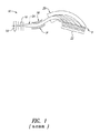
図1は、従来の二重焦点質量分析計10を示す。質量分析計10は、イオナイザー14、シャントおよびアパーチャ16、静電エネルギー分析器18、磁石20、および焦点面セクション22を備える。
FIG. 1 shows a conventional dual
操作において、ガス状または気化物質がイオナイザー14中に導入され、そこで、それは、電子によって衝突され、それ故、イオンを生成し、それは、シャントおよびアパーチャセクション16によって集束され、イオンビーム24を生成する。これらイオンの経路は、静電エネルギー分析器18により、それらの電気電荷に従って調節され、そして磁石20中の電荷/質量比に従って分離される。磁石20を出るイオンは、それらの電荷/質量比、静電エネルギー分析器18によって補償された電気的性質に従って空間的に分離および分配される。エネルギー分析器18および磁石20の物理学は、選択された範囲の比率内の任意の電荷質量比のイオンが、共通面P中で最大解像度の点に到達するように選択される。この平面Pは、質量分析計の焦点面と称される。
In operation, gaseous or vaporized material is introduced into the ionizer 14 where it is bombarded by electrons and thus produces ions that are focused by the shunt and
本明細書の背景のセクションでより詳細に記載されるように、この焦点面セクション22は、この焦点面Pを横切るイオンの位置、およびその上の任意の所定の点で平面Pを横切るイオンの相対量を検出および記録するような形態の、センサー、増幅器、およびプロセッサーを含む。従って、この焦点面セクション22のセンサーは、焦点面Pを横切る個々のイオン、およびこの面Pの共通点で横切るイオンの大きな質量に感受性であることが所望される。さらに、解像度は、異なるが非常に類似している質量電荷比を有するイオン間の鑑別を可能にするために重要である。
As described in more detail in the background section of this specification, this
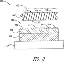
図2を参照して、1つの例示の実施形態による焦点面検出器アセンブリ100が示される。検出器アセンブリ100は、伝導性メッシュ102、マイクロチャネルプレート(MCP)104、ストリップ電荷検出器アレイ(SCD)106、絶縁体108、シリコン基板110、およびアセンブリマウント112を含む。この検出器アセンブリ100は、図1に描写されるもののように、メッシュ102が、質量分析計の焦点面Pと同一平面上にあるような形態で、かつ位置決めされる。
With reference to FIG. 2, a focal plane detector assembly 100 according to one exemplary embodiment is shown. The detector assembly 100 includes a
SCD106および絶縁体108は、半導体基板110上に公知の半導体製造技法を用いて形成される。このSCD106は、論理回路、プロセッサー、メモリーなどに連結された複数の検出器電極を備える。
The
マイクロチャネルプレート104は、第1の面118から第2の面120まで通過する複数のキャピラリー管116を含む。この第2の面120は、図2に示されるように、第1の面118と対向され得る。このMCP104の第1の面118および第2の面120は、各々、電気電荷を受容するような形態の伝導層を含む。
The
用語「第1の面」は、本明細書では、イオンの入来するストリームに面するデバイスの面または側面を一般にいうために用いられ、そして「第2の面」は、この第1の面とは反対の面または側面をいうために用いられる。 The term “first surface” is used herein to refer generally to the surface or side of the device that faces the incoming stream of ions, and “second surface” refers to this first surface. Is used to refer to the opposite side or side.
操作において、上記MCP104の第1の面は、第2の面120に対して負電圧電位で維持される。例えば、第1の面118は、−1400ボルトの電圧電位を有し得、その一方、第2の面120は、−500ボルトの電圧電位を有し、この第1の面118から第2の面120まで900ボルトの電圧差を生じる。イオンがこのMCP104の第1の面118を打つとき、それは、管116の1つに入り、そして管116の側壁を衝撃する。このイオンの衝撃は、多くの電子がこの側壁から発するようにする。
In operation, the first surface of the
第2の面120の第1の面118に対する正電荷のため、管116の側壁から発射された電子は、第2の面120に向かって引かれる。電子が管116の下に移動するとき、電子は、次いで、各々側壁を打ち、それからさらなる電子が発射されるようにする。このプロセスは、電子の雲が、MCP104の第2の面で管116を出るまで継続する。管116を出る電子は、MCP104とストリップ電荷検出器アレイ106との間の空間中に支出される。このストリップ電荷検出器アレイ106の電極114を打つ電子114は、個々の電極114中に電流を誘導し、これは、検出回路によって検出される。電子は、MCP104の第2の面120から外方にすべての方向で支出されるので、MCP104の第2の面とストリップ電荷検出器アレイ106との間の空間は、解像度を維持するために、可能な限りともに緊密に維持されることが所望される。
Due to the positive charge of the
1つの実施形態によれば、このMCP104は、第1の面118から第2の面120まで、500ボルトより大きい電圧差異を有する。
According to one embodiment, the
再び図1を参照して、イオン24のストリームは、焦点面Pに対して鋭い角度で磁石20に入ることが観察される。イオナイザー14中でサンプルをイオン化するプロセスは、このサンプルの分子から1つ以上の電子を除去することを含む。従って、上記イオンビーム24中のイオンは、正に電荷される。イオンが磁石20に入るとき、磁力は、それらの個々の質量/重量比に従って、個々のイオンの経路を曲げる。しかし、MCP104の第1の面118における高負電圧は、磁石20中の正に電荷したイオンに誘引的である電場を生成する。従って、これらイオンの経路は、MCP104の表面上の負電荷によって所望されずに歪められ得る。
Referring again to FIG. 1, it is observed that the stream of
上記検出器アレイ100が、焦点面Pで適正に位置決めされるとき、メッシュ102が、MCP104と磁石20の背面との間に位置決めされ、そして低電位電圧で提供される。例えば、メッシュ102は、回路接地に電気的に連結され得るか、または100ボルト未満の電圧で維持され得る。このメッシュ102は、MCP104の強力な負電場をブロックするために供され、その電場が、イオンが焦点面Pに接近するとき、イオンの経路に影響することを防ぐ。電場をブロックする際のメッシュ102の有効性は、メッシュ102中の開口部のサイズに反比例する。その一方、メッシュの材料に実際に接触するイオンはMCPと接触するようには通過しないので、メッシュ102がイオンに対して実質的に透明であることが所望される。これらの制約があるので、80%または90%を超える開口面積を有する非常に微細なメッシュ102が好ましい。このメッシュ102は、0.5ミリメートル未満の厚みを有し得る。
When the detector array 100 is properly positioned at the focal plane P, the
ここで、図3を参照して、図1に示される磁石20と同様に磁石122がそれに取り付けられたメッシュ102とともに提供される。図3の実施形態では、メッシュ102および磁石122は、接地電位で維持される。その他の実施形態では、メッシュ102は、磁石122から分離され得、そして異なる電位で維持されるが、メッシュ102と磁石122との間の電圧差異は最小であることが好ましい。例えば、1つの実施形態によれば、このメッシュ102は、磁石122の電位に対して500ボルト未満で維持される。別の実施形態によれば、このメッシュ102は、100ボルト、絶対値未満で維持される。
Referring now to FIG. 3, a
用語「絶対値」は、本明細書では、極性への参照なくして電圧電位をいうために用いられる。 The term “absolute value” is used herein to refer to a voltage potential without reference to polarity.
図4および5を参照して、焦点面検出器アセンブリ130が、別の例示の実施形態に従って示される。この検出器アセンブリ130は、第1の電極、第2の電極、第3の電極および第4の電極134〜137を備え、第1のMCP138および第2のMCP140、絶縁スペーサー142、144、検出器マウント146、およびアセンブリホルダー132を備える。
4 and 5, a focal
このアセンブリ130は、図5に概略が示される。このアセンブリ130は、アセンブリホルダー132によって支持されるベースに取り付けられるような形態である。ファスナー(図示せず)が、アセンブリホルダー132に検出器マウント146を付勢し、それらのその他の構成要素を間に挟持する。先に図2のMCP104を参照して説明したように、MCPは、電子カスケードを増幅する。このアセンブリ130の場合には、第1のMCP138は、焦点面を通過するイオンを受容し、そして応答で電子のカスケードを生成するような形態である。第2のMCP140は、第1のMCP138から電子を受容し、そしてイオンのカスケードを増幅し、そしてストリップ電荷検出器アレイ106により強い信号を提供する。第1の電極、第2の電極、第3の電極および第4の電極134〜137は、各々、個々のMCPの第1の面および第2の面にエネルギーを与えるためにターミナル148を経由して電圧電荷が提供される。第1の絶縁スペーサー142および第2のスペーサー144は、アセンブリ130の構成要素を電気的に絶縁するために提供される。アセンブリホルダー132もまた、非伝導性であり得、検出器アセンブリ130を、メッシュ102およびそれが採用される質量分析計のその他の構成要素から絶縁するか、または別個の絶縁体を含み得る。
This
1つの実施形態によれば、各MCP138、140の第1の面を第2の面に横切る電圧差異は、約500〜900ボルトの範囲であり、そして個々の電極134〜137で提供される。さらに、第2の電極135と第3の電極136との間の電圧差異はゼロに等しいがまたはゼロより大きい。
According to one embodiment, the voltage difference across the first side of each
このアセンブリの構成要素は、このアセンブリの解像度を最大にするために、電気接触なくして可能な限りともに緊密に間隔を置かれ得る。例えば、1つの実施形態によれば、メッシュ102は、焦点面Pに直接、またはその1ミリメートル内に配置される。第1のMCP138の第1の面139は、メッシュ102の2ミリメートル内に位置決めされ得、そして好ましくは0.5ミリメートル内である。本発明の実施形態によれば、第2のMCP140の第1の面145は、第1のMCP138の第2の面141の2ミリメートル内に位置決めされる。そして好ましくは0.5ミリートル以内である。
The components of the assembly can be spaced as closely together as possible without electrical contact to maximize the resolution of the assembly. For example, according to one embodiment, the
1つの実施形態によれば、第1のMCP138の第1の面139は、電場が生成され、それによって、磁石122の作動を妨害するに十分な強度を有さないように、比較的低い電圧レベルで維持される。例えば、この第1のMCP138の第1の面139は、100ボルト絶対値未満の電位を有し得る。このアセンブリのその他の構成要素の電圧レベルは、上記で概説したような所望の電圧差異を維持するよう選択される。この実施形態によれば、メッシュ102は必要ではない。なぜなら、感知し得る電場がないからである。
According to one embodiment, the
ここで図6を参照して、別の実施形態が示される。この実施形態では、焦点面検出器アセンブリ150が提供される。図6のアセンブリ150と図4および5のアセンブリ130との間の主な差異は、アセンブリ150が単一のMCP138のみを有するとして示される点にある。その他の局面では、アセンブリ150と130とは極めて類似している。図6はまた、質量分析計160の種々の構成要素を受容する形態のベースプレート152を示す。磁石122は、ベースプレート152上に位置決めされて示され、そしてメッシュ102は、分析計160の焦点面Pに位置決めされて示される。ファスナー154は、検出器マウント146およびアセンブリホルダー132を、線Fに沿ってベースプレート152に固定する位置で示される。図4および5のアセンブリ130は、類似の様式でベースプレートに取り付けられる類似の形態であることが認識される。
Referring now to FIG. 6, another embodiment is shown. In this embodiment, a focal
図6に示されるデバイスでは、焦点面Pは、磁石122の面と同一平面にある。その他の実施形態では、焦点面Pは、特定距離だけ磁石122から分離され得る。例えば、1つの実施形態によれば、分析計システムは、焦点面が磁石の背面から間隔を置かれ、メッシュ102が焦点面と磁石の背面との間にあり、そしてMCPの第1の面から小距離分離され、その一方、MCPの第1の面は、焦点面に正確に位置決めされるような形態である。
In the device shown in FIG. 6, the focal plane P is coplanar with the surface of the
メッシュ102は、磁石122の背面に取り付けられるとして説明されているが、別の実施形態によれば、メッシュ102は、アセンブリホルダー132に、このアセンブリホルダー132がメッシュと第1の電極134との間に絶縁体を形成するように取り付けられる。代替の実施形態によれば、メッシュ102は、アセンブリホルダー132と第1の電極134との間に位置決めされ、この場合、別の絶縁体が、メッシュ102と第1の電極134との間に提供される。
Although the
本発明を、二重焦点質量分析計を、そしてストリップ電荷検出器アレイを参照して説明した。これらの実施形態は、例示のみのために説明され、そして本発明の範囲を制限しない。例えば、この検出器アレイは、ファラデーカップ検出器アレイまたはCCDタイプ検出器アレイを含み得る。本発明の実施形態によれば、上記検出器アセンブリは、直接電荷測定デバイスを含み得る。 The present invention has been described with reference to a dual focus mass spectrometer and a strip charge detector array. These embodiments are described by way of example only and do not limit the scope of the invention. For example, the detector array may include a Faraday cup detector array or a CCD type detector array. According to embodiments of the invention, the detector assembly may include a direct charge measurement device.
本明細書で言及され、そして/または出願データシートで列挙される、すべての上記米国特許、米国特許出願公報、米国特許出願、外国特許、外国特許出願および非特許刊行物は、制限されずに、米国仮特許出願第60/557,920号;米国仮特許出願第60//577,969号;米国仮特許出願第60/550,663号;および米国仮特許出願第60/550,664号;米国特許第5,801,380号;米国非仮特許出願第10/811,576号;米国非仮特許出願第10/860,776号;米国非仮特許出願第09/744,360号;米国特許第6,576,899号;米国特許第5,317,151号、米国特許第5,801,380号、米国特許第6,182,831号、米国特許第6,191,419号、米国特許第6,403,956号;および米国特許第6,046,451号を含み、それらの全体が参考として本明細書中に援用される。 All the above U.S. patents, U.S. patent application publications, U.S. patent applications, foreign patents, foreign patent applications and non-patent publications mentioned in this specification and / or listed in the application data sheet are not limited. U.S. Provisional Patent Application No. 60 / 557,920; U.S. Provisional Patent Application No. 60 // 577,969; U.S. Provisional Patent Application No. 60 / 550,663; and U.S. Provisional Patent Application No. 60 / 550,664. U.S. Patent No. 5,801,380; U.S. Non-Tentative Application No. 10 / 811,576; U.S. Non-Tentative Application No. 10 / 860,776; U.S. Non-Tentative Application No. 09 / 744,360; US Pat. No. 6,576,899; US Pat. No. 5,317,151, US Pat. No. 5,801,380, US Pat. No. 6,182,831, US Pat. No. 6,191,419, USA Patent No. 6,403,956; include and U.S. Patent No. 6,046,451, the entire of which are incorporated herein by reference.
さらに、J.Mattauchにより公開された事項、Ergebnisse der exakten Naturwissenschaften、第9巻、170〜236頁、1940;「焦点面検出器csの基礎」K.Birkinshaw Jrnl.of Mass Spectrometry、32巻、795〜806(1997);A.A.Scheidemann、R.B.Darling、F.J.Schumacher、およびA.Isakarov、Tech.Digest of the 14th Int.Forum on Process Analytical Chem.(IFPAC−2000)Lake Las Vegas、Nevada、1月23〜26日、2000、要約1〜067;R.B.Darling、A.A.Scheidermann、K.N.Bhat、およびT.−C.Chen.、Proc.of the 14th IEEE Int.Conf.on Micro Electro Mechanical Systems(MEMS−2001)、Interlaken、Switzerland、1月21〜25日、2001、90〜93頁;Nier、D.J.Schlutter Rev.Sci.Instrum.56(2)、214〜219頁、1985;およびT.W.Burgoyneら、J.Am.Soc.Mass Spectrum 8、307〜318頁、1997はそれらの全体が参考として援用される。 Furthermore, J. et al. Matthach, Ergebnisse der excakten Naturwissenschafften, Vol. 9, pp. 170-236, 1940; “Focus plane detector cs basics” Birkinshaw Jrnl. of Mass Spectrometry, vol. 32, 795-806 (1997); A. Scheidemann, R.M. B. Darling, F.M. J. et al. Schumacher, and A.A. Isakarov, Tech. Digest of the 14th Int. Forum on Process Analytical Chem. (IFPAC-2000) Lake Las Vegas, Nevada, January 23-26, 2000, summary 1-067; B. Darling, A.D. A. Scheidermann, K.M. N. Bhat, and T.W. -C. Chen. Proc. of the 14th IEEE Int. Conf. on Micro Electro Mechanical Systems (MEMS-2001), Interlaken, Switzerland, January 21-25, 2001, pages 90-93; Nier, D. et al. J. et al. Schlitter Rev. Sci. Instrum. 56 (2), 214-219, 1985; W. Burgoyne et al. Am. Soc. Mass Spectrum 8, pages 307-318, 1997 are incorporated by reference in their entirety.
前述から、本発明の詳細な実施形態が例示の目的のために本明細書中に説明されているが、種々の改変が本発明の思想および範囲から逸脱することなくなされ得ることが認識される。従って、本発明は、添付の請求項によることを除いて制限されない。 From the foregoing, it will be appreciated that although detailed embodiments of the invention have been described herein for purposes of illustration, various modifications may be made without departing from the spirit and scope of the invention. . Accordingly, the invention is not limited except as by the appended claims.
Claims (29)
該質量分析計の焦点面に平行な第1の平面にある第1の面を有するイオン検出器であって、該イオン検出器が:
第1のマイクロチャネルプレート電子増倍管であって、該第1のマイクロチャネルプレート電子増倍管の第1の面が該イオン検出器の第1の面を規定する第1のマイクロチャネルプレート電子増倍管;および
該第1のマイクロチャネルプレート電子増倍管の第2の面から発する電子を検出するように位置決めされ、かつ形態とされるCCD検出器アレイ、を備える、イオン検出器;ならびに
該質量分析計の焦点面に平行な第2の平面にあり、そして第1の電圧電位を有する電気伝導性メッシュであって、該質量分析計の磁石を出るイオンが、該イオン検出器に接触する前に該メッシュを通過するよう配置されている、メッシュ、を備える、アセンブリ。A focal plane detector assembly for a mass spectrometer comprising:
An ion detector having a first surface in a first plane parallel to the focal plane of the mass spectrometer, the ion detector comprising:
A first microchannel plate electron multiplier, wherein the first surface of the first microchannel plate electron multiplier defines the first surface of the ion detector. An ion detector comprising: a multiplier; and a CCD detector array positioned and configured to detect electrons emanating from the second surface of the first microchannel plate electron multiplier; An electrically conductive mesh in a second plane parallel to the focal plane of the mass spectrometer and having a first voltage potential, wherein ions exiting the mass spectrometer magnet contact the ion detector An assembly, arranged to pass through the mesh prior to.
前記第1のマイクロチャネルプレート電子増倍管と前記CCD検出器アレイとの間に位置決めされる少なくとも第2のマイクロチャネルプレート電子増倍管を備える、請求項1に記載のアセンブリ。The ion detector is:
The assembly of claim 1, comprising at least a second microchannel plate electron multiplier positioned between the first microchannel plate electron multiplier and the CCD detector array.
第1のマイクロチャネルプレート電子増倍管であって、該第1のマイクロチャネルプレート電子増倍管の第1の面が、該質量分析計の焦点面に平行な第1の平面にあり、そして該質量分析計の磁石に面し、該磁石に対して100ボルト未満の電圧差異を有する、第1のマイクロチャネルプレート電子増倍管;および
該第1のマイクロチャネルプレート電子増倍管の第2の面から発する電子を検出するように位置決めされ、かつ形態にあるCCD検出器アレイ、を備える、アセンブリ。A focal plane detector assembly for a mass spectrometer comprising:
A first microchannel plate electron multiplier, wherein the first surface of the first microchannel plate electron multiplier is in a first plane parallel to the focal plane of the mass spectrometer; and A first microchannel plate electron multiplier facing the magnet of the mass spectrometer and having a voltage difference of less than 100 volts relative to the magnet; and a second of the first microchannel plate electron multiplier An assembly comprising a CCD detector array positioned and configured to detect electrons emanating from the surface of the device.
前記第1のマイクロチャネルプレート電子増倍管と前記検出器アレイとの間に位置決めされる少なくとも第2のマイクロチャネルプレート電子増倍管を備える、請求項19に記載のアセンブリ。further:
The assembly of claim 19, comprising at least a second microchannel plate electron multiplier positioned between the first microchannel plate electron multiplier and the detector array.
焦点合わせされたストリームでイオンを発するような形態であるイオン供給源;
該イオンのストリームのイオンの少なくとも一部分を受容するような形態である焦点面検出器であって、該焦点面検出器が:
マイクロチャネルプレート電子増倍管;および
該マイクロチャネルプレート電子増倍管から発する電子を検出するように位置決めされるCCD検出器アレイを備える、焦点面検出器;ならびに
該イオンが該分析計の焦点面に到達するまで、該焦点面検出器における電圧電位から該ストリームのイオンを遮蔽するための遮蔽手段、を備える、質量分析計。Mass spectrometer:
An ion source that is configured to emit ions in a focused stream;
A focal plane detector configured to receive at least a portion of ions of the stream of ions, the focal plane detector comprising:
A focal plane detector comprising: a microchannel plate electron multiplier; and a CCD detector array positioned to detect electrons emanating from the microchannel plate electron multiplier; and a focal plane of the analyzer where the ions are A mass spectrometer comprising shielding means for shielding ions of the stream from the voltage potential at the focal plane detector until reaching
個々のイオンの電荷/質量比に従って該ビームのイオンを曲げる工程;
該ビームのイオンに影響し得る電場をマイクロチャネルプレート電子増倍管において生成する工程;
該ビームのイオンが電気伝導性メッシュを通過するまで、該電場から該ビームのイオンを遮蔽する工程;
該ビームのイオンを該マイクロチャネルプレート電子増倍管に受容する工程;および
CCD検出器アレイを用いて、該マイクロチャネルプレート電子増倍管を出る電子を検出する工程、を包含する、方法。Generating a beam of ions;
Bending the ions of the beam according to the charge / mass ratio of the individual ions;
Generating an electric field in a microchannel plate electron multiplier that can affect the ions of the beam;
Shielding the beam ions from the electric field until the beam ions pass through an electrically conductive mesh;
Receiving ions of the beam into the microchannel plate electron multiplier; and detecting electrons exiting the microchannel plate electron multiplier using a CCD detector array.
Applications Claiming Priority (9)
| Application Number | Priority Date | Filing Date | Title |
|---|---|---|---|
| US55066404P | 2004-03-05 | 2004-03-05 | |
| US55066304P | 2004-03-05 | 2004-03-05 | |
| US60/550,663 | 2004-03-05 | ||
| US60/550,664 | 2004-03-05 | ||
| US55796904P | 2004-03-31 | 2004-03-31 | |
| US55792004P | 2004-03-31 | 2004-03-31 | |
| US60/557,920 | 2004-03-31 | ||
| US60/557,969 | 2004-03-31 | ||
| PCT/US2005/007128 WO2005088672A2 (en) | 2004-03-05 | 2005-03-04 | Focal plane detector assembly of a mass spectrometer |
Publications (3)
| Publication Number | Publication Date |
|---|---|
| JP2007527601A JP2007527601A (en) | 2007-09-27 |
| JP2007527601A5 JP2007527601A5 (en) | 2008-04-17 |
| JP4931793B2 true JP4931793B2 (en) | 2012-05-16 |
Family
ID=34961731
Family Applications (1)
| Application Number | Title | Priority Date | Filing Date |
|---|---|---|---|
| JP2007502023A Active JP4931793B2 (en) | 2004-03-05 | 2005-03-04 | Mass spectrometer focal plane detector assembly |
Country Status (4)
| Country | Link |
|---|---|
| US (2) | US7550722B2 (en) |
| EP (1) | EP1721330A2 (en) |
| JP (1) | JP4931793B2 (en) |
| WO (2) | WO2005088671A2 (en) |
Families Citing this family (24)
| Publication number | Priority date | Publication date | Assignee | Title |
|---|---|---|---|---|
| EP1073894B1 (en) * | 1998-10-06 | 2010-10-06 | The University Of Washington | Charged particle beam detection system |
| DE102006004478A1 (en) * | 2006-01-30 | 2007-08-02 | Spectro Analytical Instruments Gmbh & Co. Kg | Device for detecting particles for a mass spectrometer comprises trenches arranged between neighboring structures in the radiation direction |
| WO2007138679A1 (en) * | 2006-05-30 | 2007-12-06 | Shimadzu Corporation | Mass spectrometer |
| US7339169B1 (en) | 2006-11-29 | 2008-03-04 | Lawrence Livermore National Security, Llc | Sample rotating turntable kit for infrared spectrometers |
| DE102007052794A1 (en) * | 2007-11-02 | 2009-05-07 | Schwarzer, Robert, Prof. Dr. | Device for crystal orientation measurement by means of an ion-blocking pattern and a focused ion probe |
| JP5452038B2 (en) * | 2009-03-06 | 2014-03-26 | 浜松ホトニクス株式会社 | Electron multiplier and electron detector |
| US8549893B2 (en) | 2009-03-06 | 2013-10-08 | Thermo Finnigan Llc | System and method for a gas chromatograph to mass spectrometer interface |
| JP5210940B2 (en) * | 2009-03-31 | 2013-06-12 | 浜松ホトニクス株式会社 | Mass spectrometer |
| GB2478984A (en) | 2010-03-26 | 2011-09-28 | Hexcel Composites Ltd | Curable composite material |
| US11081331B2 (en) * | 2015-10-28 | 2021-08-03 | Duke University | Mass spectrometers having segmented electrodes and associated methods |
| US10872755B2 (en) * | 2016-03-17 | 2020-12-22 | Leidos, Inc. | Low power mass analyzer and system integrating same for chemical analysis |
| MX2020011575A (en) | 2018-04-30 | 2021-01-20 | Leidos Inc | An improved low-power mass interrogation system and assay for determining vitamin d levels. |
| GB201808890D0 (en) | 2018-05-31 | 2018-07-18 | Micromass Ltd | Bench-top time of flight mass spectrometer |
| GB201808894D0 (en) | 2018-05-31 | 2018-07-18 | Micromass Ltd | Mass spectrometer |
| GB201808936D0 (en) | 2018-05-31 | 2018-07-18 | Micromass Ltd | Bench-top time of flight mass spectrometer |
| GB201808912D0 (en) | 2018-05-31 | 2018-07-18 | Micromass Ltd | Bench-top time of flight mass spectrometer |
| US11373849B2 (en) | 2018-05-31 | 2022-06-28 | Micromass Uk Limited | Mass spectrometer having fragmentation region |
| GB201808949D0 (en) | 2018-05-31 | 2018-07-18 | Micromass Ltd | Bench-top time of flight mass spectrometer |
| GB201808892D0 (en) | 2018-05-31 | 2018-07-18 | Micromass Ltd | Mass spectrometer |
| GB2576077B (en) | 2018-05-31 | 2021-12-01 | Micromass Ltd | Mass spectrometer |
| CN109031452B (en) * | 2018-06-29 | 2019-11-12 | 北京空间机电研究所 | A kind of the splicing focal plane subassembly and joining method of multispectral section of detector |
| CN108962717B (en) * | 2018-08-09 | 2024-01-26 | 金华职业技术学院 | Mass spectrometer for researching macromolecules and method for researching electric charge quantity |
| JP6734449B1 (en) * | 2019-08-02 | 2020-08-05 | 浜松ホトニクス株式会社 | Ion detector, measuring device and mass spectrometer |
| JP7252179B2 (en) * | 2020-07-08 | 2023-04-04 | 浜松ホトニクス株式会社 | Ion detectors, measurement devices and mass spectrometers |
Family Cites Families (85)
| Publication number | Priority date | Publication date | Assignee | Title |
|---|---|---|---|---|
| US2309414A (en) * | 1939-10-24 | 1943-01-26 | Gen Electric | Damping magnet system |
| GB650861A (en) | 1948-10-01 | 1951-03-07 | Jack Blears | Improvements relating to magnet systems for mass spectrometers |
| GB674729A (en) | 1949-04-13 | 1952-07-02 | Mullard Radio Valve Co Ltd | Mass spectrographs and like apparatus |
| US2964627A (en) * | 1957-07-01 | 1960-12-13 | Trub Tauber & Co A G | Double-focussing spectrometer for electrically charged particles |
| US3478204A (en) * | 1964-08-24 | 1969-11-11 | Jean R Berry | Mass spectrometer ion source having a laser to cause autoionization of gas |
| US3521054A (en) * | 1968-02-29 | 1970-07-21 | Webb James E | Analytical photoionization mass spectrometer with an argon gas filter between the light source and monochrometer |
| US3555331A (en) * | 1968-08-08 | 1971-01-12 | Susquehanna Corp | Apparatus for maintaining vacuum conditions by molecular depletion of gas |
| SE358254B (en) | 1971-09-15 | 1973-07-23 | K Linderoth | |
| US3898456A (en) * | 1974-07-25 | 1975-08-05 | Us Energy | Electron multiplier-ion detector system |
| US4016421A (en) * | 1975-02-13 | 1977-04-05 | E. I. Du Pont De Nemours And Company | Analytical apparatus with variable energy ion beam source |
| US4071848A (en) * | 1976-11-26 | 1978-01-31 | Bell Telephone Laboratories, Incorporated | Thinned aperiodic antenna arrays with improved peak sidelobe level control |
| US4182984A (en) * | 1978-05-05 | 1980-01-08 | Westinghouse Electric Corp. | Magnetic damping assembly with temperature compensator for watthour meters |
| DE3014053A1 (en) * | 1980-04-11 | 1981-10-15 | Max-Planck-Gesellschaft zur Förderung der Wissenschaften e.V., 3400 Göttingen | CONTROL ARRANGEMENT FOR A MASS SPECTROMETER |
| JPS57191952A (en) * | 1981-05-22 | 1982-11-25 | Jeol Ltd | Mass spectrograph |
| US4456898A (en) * | 1982-02-11 | 1984-06-26 | General Electric Company | Thermal compensators for magnetic circuits |
| FR2544914B1 (en) * | 1983-04-19 | 1986-02-21 | Cameca | IMPROVEMENTS TO MASS SPECTROMETERS |
| US4476732A (en) * | 1983-04-21 | 1984-10-16 | Varian Associates, Inc. | Septumless jet stream on-column injector for chromatography |
| DE3510378A1 (en) * | 1985-03-22 | 1986-10-02 | Coulston International Corp., Albany, N.Y. | METHOD FOR THE ANALYTICAL DETERMINATION OF ORGANIC SUBSTANCES |
| DE3710935C2 (en) * | 1986-04-23 | 1994-08-18 | Finnigan Mat Gmbh | Method for operating a mass spectrometer and mass spectrometer for performing the method |
| US4855747A (en) * | 1987-08-17 | 1989-08-08 | Trustees Of The University Of Pennsylvania | Method of target imaging and identification |
| US4859848A (en) * | 1987-10-09 | 1989-08-22 | Masstron, Inc. | Mass spectrometer apparatus |
| FR2640697B1 (en) * | 1988-12-16 | 1993-01-08 | Cit Alcatel | PUMPING ASSEMBLY FOR PROVIDING HIGH VACUUMS |
| FR2640821B1 (en) * | 1988-12-16 | 1991-05-31 | Thomson Csf | ANTENNA WITH THREE-DIMENSIONAL COVERAGE AND ELECTRONIC SCANNING, OF THE RAREFIELD RANDOM VOLUME NETWORK TYPE |
| JPH0812773B2 (en) * | 1989-04-11 | 1996-02-07 | 日本電子株式会社 | Simultaneous detection mass spectrometer |
| US5299577A (en) * | 1989-04-20 | 1994-04-05 | National Fertility Institute | Apparatus and method for image processing including one-dimensional clean approximation |
| US5313061A (en) * | 1989-06-06 | 1994-05-17 | Viking Instrument | Miniaturized mass spectrometer system |
| US5231591A (en) * | 1989-09-11 | 1993-07-27 | Nellcor Incorporated | Agent gas analyzer and method of use |
| US5046018A (en) * | 1989-09-11 | 1991-09-03 | Nellcor, Inc. | Agent gas analyzer and method of use |
| US4988867A (en) * | 1989-11-06 | 1991-01-29 | Galileo Electro-Optics Corp. | Simultaneous positive and negative ion detector |
| GB8928917D0 (en) * | 1989-12-21 | 1990-02-28 | Vg Instr Group | Method and apparatus for surface analysis |
| US5135870A (en) * | 1990-06-01 | 1992-08-04 | Arizona Board Of Regents | Laser ablation/ionizaton and mass spectrometric analysis of massive polymers |
| GB2249426A (en) | 1990-10-31 | 1992-05-06 | Dennis Leigh Technology Limite | Mass spectrometer |
| JPH04326943A (en) * | 1991-04-25 | 1992-11-16 | Hitachi Ltd | Vacuum exhaust system and exhaust method |
| US5461235A (en) * | 1991-06-21 | 1995-10-24 | Cottrell; John S. | Mass spectrometry apparatus and method relating thereto |
| US5382793A (en) * | 1992-03-06 | 1995-01-17 | Hewlett-Packard Company | Laser desorption ionization mass monitor (LDIM) |
| US5264813A (en) * | 1992-05-19 | 1993-11-23 | Caterpillar Inc. | Force motor having temperature compensation characteristics |
| US5317151A (en) * | 1992-10-30 | 1994-05-31 | Sinha Mahadeva P | Miniaturized lightweight magnetic sector for a field-portable mass spectrometer |
| US5331158A (en) * | 1992-12-07 | 1994-07-19 | Hewlett-Packard Company | Method and arrangement for time of flight spectrometry |
| US5490765A (en) * | 1993-05-17 | 1996-02-13 | Cybor Corporation | Dual stage pump system with pre-stressed diaphragms and reservoir |
| US5386115A (en) * | 1993-09-22 | 1995-01-31 | Westinghouse Electric Corporation | Solid state micro-machined mass spectrograph universal gas detection sensor |
| GB9409953D0 (en) * | 1994-05-17 | 1994-07-06 | Fisons Plc | Mass spectrometer and electron impact ion source therefor |
| JP3128053B2 (en) * | 1995-05-30 | 2001-01-29 | 株式会社島津製作所 | Gas chromatograph mass spectrometer |
| DE19524609A1 (en) * | 1995-07-06 | 1997-01-09 | Leybold Ag | Device for the rapid evacuation of a vacuum chamber |
| US6135971A (en) * | 1995-11-09 | 2000-10-24 | Brigham And Women's Hospital | Apparatus for deposition of ultrasound energy in body tissue |
| US5801380A (en) * | 1996-02-09 | 1998-09-01 | California Institute Of Technology | Array detectors for simultaneous measurement of ions in mass spectrometry |
| US5808299A (en) * | 1996-04-01 | 1998-09-15 | Syagen Technology | Real-time multispecies monitoring by photoionization mass spectrometry |
| EP0898784A4 (en) * | 1996-04-12 | 2006-08-02 | Perkin Elmer Corp | Ion detector, detector array and instrument using same |
| US6051832A (en) * | 1996-08-20 | 2000-04-18 | Graseby Dynamics Limited | Drift chambers |
| DE19644713A1 (en) * | 1996-10-28 | 1998-05-07 | Bruker Franzen Analytik Gmbh | High-resolution high-mass detector for time-of-flight mass spectrometers |
| US6316768B1 (en) * | 1997-03-14 | 2001-11-13 | Leco Corporation | Printed circuit boards as insulated components for a time of flight mass spectrometer |
| US5929819A (en) * | 1996-12-17 | 1999-07-27 | Hughes Electronics Corporation | Flat antenna for satellite communication |
| US6191419B1 (en) * | 1997-08-06 | 2001-02-20 | California Institute Of Technology | Machined electrostatic sector for mass spectrometer |
| CA2304868A1 (en) | 1997-09-23 | 1999-04-01 | Ciphergen Biosystems, Inc | Secondary ion generator detector for time-of-flight mass spectrometry |
| WO1999017865A1 (en) | 1997-10-07 | 1999-04-15 | University Of Washington | Magnetic separator for linear dispersion and method for producing the same |
| US6403956B1 (en) * | 1998-05-01 | 2002-06-11 | California Institute Of Technology | Temperature compensation for miniaturized magnetic sector |
| US6155097A (en) * | 1998-05-29 | 2000-12-05 | Varian, Inc. | Method and apparatus for selectively extracting and compressing trace samples from a carrier to enhance detection |
| US6195705B1 (en) * | 1998-06-30 | 2001-02-27 | Cisco Technology, Inc. | Mobile IP mobility agent standby protocol |
| US6300626B1 (en) * | 1998-08-17 | 2001-10-09 | Board Of Trustees Of The Leland Stanford Junior University | Time-of-flight mass spectrometer and ion analysis |
| EP1073894B1 (en) | 1998-10-06 | 2010-10-06 | The University Of Washington | Charged particle beam detection system |
| US6198096B1 (en) * | 1998-12-22 | 2001-03-06 | Agilent Technologies, Inc. | High duty cycle pseudo-noise modulated time-of-flight mass spectrometry |
| JP2001015011A (en) * | 1999-06-30 | 2001-01-19 | Horiba Ltd | Ferroelectric photoelectric device |
| US6635883B2 (en) * | 1999-12-06 | 2003-10-21 | Epion Corporation | Gas cluster ion beam low mass ion filter |
| US6614019B2 (en) * | 2000-01-20 | 2003-09-02 | W. Bruce Feller | Mass spectrometry detector |
| US6858839B1 (en) * | 2000-02-08 | 2005-02-22 | Agilent Technologies, Inc. | Ion optics for mass spectrometers |
| US6831276B2 (en) * | 2000-05-08 | 2004-12-14 | Philip S. Berger | Microscale mass spectrometric chemical-gas sensor |
| US6734423B2 (en) * | 2000-05-31 | 2004-05-11 | The Johns Hopkins University | Pulsed laser sampling for mass spectrometer system |
| RU2182347C2 (en) * | 2000-08-04 | 2002-05-10 | Институт физики полупроводников СО РАН | Acoustooptical tunable filter |
| US6576899B2 (en) * | 2001-01-16 | 2003-06-10 | California Institute Of Technology | Direct detection of low-energy charged particles using metal oxide semiconductor circuitry |
| US6847039B2 (en) * | 2001-03-28 | 2005-01-25 | Canon Kabushiki Kaisha | Photodetecting device, radiation detecting device, and radiation imaging system |
| SE0101555D0 (en) * | 2001-05-04 | 2001-05-04 | Amersham Pharm Biotech Ab | Fast variable gain detector system and method of controlling the same |
| TW589723B (en) * | 2001-09-10 | 2004-06-01 | Ebara Corp | Detecting apparatus and device manufacturing method |
| US6649908B2 (en) * | 2001-09-20 | 2003-11-18 | Agilent Technologies, Inc. | Multiplexing capillary array for atmospheric pressure ionization-mass spectrometry |
| US6747258B2 (en) * | 2001-10-09 | 2004-06-08 | Itt Manufacturing Enterprises, Inc. | Intensified hybrid solid-state sensor with an insulating layer |
| US6646256B2 (en) * | 2001-12-18 | 2003-11-11 | Agilent Technologies, Inc. | Atmospheric pressure photoionization source in mass spectrometry |
| CA2475132A1 (en) * | 2002-02-20 | 2003-08-28 | University Of Washington | Analytical instruments using a pseudorandom array of sample sources, such as a micro-machined mass spectrometer or monochromator |
| AU2003224671A1 (en) * | 2002-03-08 | 2003-09-22 | Aventis Pharmaceuticals, Inc. | Preparative separation of mixtures by mass spectrometry |
| US6680477B2 (en) * | 2002-05-31 | 2004-01-20 | Battelle Memorial Institute | High spatial resolution matrix assisted laser desorption/ionization (MALDI) |
| US6838663B2 (en) * | 2002-05-31 | 2005-01-04 | University Of Florida | Methods and devices for laser desorption chemical ionization |
| KR100449876B1 (en) * | 2002-12-05 | 2004-09-22 | 삼성전기주식회사 | A multi-layer PCB for connecting multi-channel optical signals of block type, and methods thereof |
| KR100451635B1 (en) * | 2002-12-10 | 2004-10-08 | 삼성전기주식회사 | Fiber blocks and pipe blocks, and methods for connecting optical signals of multi-layer PCB by using them |
| US20060076482A1 (en) * | 2002-12-13 | 2006-04-13 | Hobbs Steven E | High throughput systems and methods for parallel sample analysis |
| KR100525223B1 (en) * | 2002-12-24 | 2005-10-28 | 삼성전기주식회사 | An optical printed circuit board for transmitting of signals long-distance |
| KR100499005B1 (en) * | 2002-12-27 | 2005-07-01 | 삼성전기주식회사 | A printed circuit board being packaged optical devices of multi-channel block type |
| US20040222374A1 (en) * | 2003-05-07 | 2004-11-11 | Scheidemann Adi A. | Ion detector array assembly and devices comprising the same |
| US6979818B2 (en) * | 2003-07-03 | 2005-12-27 | Oi Corporation | Mass spectrometer for both positive and negative particle detection |
-
2005
- 2005-03-04 US US11/073,426 patent/US7550722B2/en active Active
- 2005-03-04 JP JP2007502023A patent/JP4931793B2/en active Active
- 2005-03-04 WO PCT/US2005/007197 patent/WO2005088671A2/en active Application Filing
- 2005-03-04 US US11/071,992 patent/US20060011829A1/en not_active Abandoned
- 2005-03-04 EP EP05732599A patent/EP1721330A2/en not_active Withdrawn
- 2005-03-04 WO PCT/US2005/007128 patent/WO2005088672A2/en not_active Application Discontinuation
Also Published As
| Publication number | Publication date |
|---|---|
| WO2005088671A3 (en) | 2006-11-09 |
| US20060011829A1 (en) | 2006-01-19 |
| WO2005088672A3 (en) | 2006-08-10 |
| JP2007527601A (en) | 2007-09-27 |
| WO2005088672A2 (en) | 2005-09-22 |
| EP1721330A2 (en) | 2006-11-15 |
| US7550722B2 (en) | 2009-06-23 |
| US20060011826A1 (en) | 2006-01-19 |
| WO2005088671A2 (en) | 2005-09-22 |
Similar Documents
| Publication | Publication Date | Title |
|---|---|---|
| JP4931793B2 (en) | Mass spectrometer focal plane detector assembly | |
| US9543138B2 (en) | Ion optical system for MALDI-TOF mass spectrometer | |
| EP2297763B1 (en) | Charged particle detection system and method | |
| JP2009523300A (en) | Focused mass spectrometer ion guide, spectrometer and method | |
| US5464975A (en) | Method and apparatus for charged particle collection, conversion, fragmentation or detection | |
| JP6254612B2 (en) | Mass spectrometer with optimized magnetic shunt | |
| JPH11345591A (en) | Cycloid mass spectrometer and ionizer for use therein | |
| JP2023526078A (en) | Apparatus and method for high performance charged particle detection | |
| US5665966A (en) | Current measuring system | |
| US9564306B2 (en) | Mass spectrometer with improved magnetic sector | |
| JP6535250B2 (en) | Charged particle detector and control method thereof | |
| JP6676383B2 (en) | Time-of-flight mass spectrometer | |
| US8610055B1 (en) | Mass spectrometer ion trap having asymmetric end cap apertures | |
| US9640378B2 (en) | Time-of-flight mass spectrometer | |
| EP1533828A1 (en) | Ion detector | |
| JP2015519717A (en) | Compact time-of-flight mass spectrometer | |
| JPWO2018092271A1 (en) | Ion analyzer | |
| WO2019244805A1 (en) | Mcp assembly and charged particle detector | |
| JP2022545651A (en) | focal plane detector | |
| JP6717429B2 (en) | Ion detector and mass spectrometer | |
| JP2006221876A (en) | Ion detector, mass spectrometer having the same, and method for operating ion detector | |
| US9589776B2 (en) | Ruggedized advanced identification mass spectrometer | |
| WO2022024398A1 (en) | Ion trap and mass spectrometer | |
| Appelhans et al. | Wide dispersion multiple collector isotope ratio mass spectrometer | |
| RU2272334C1 (en) | Gas mixture analyzing device |
Legal Events
| Date | Code | Title | Description |
|---|---|---|---|
| A521 | Request for written amendment filed |
Free format text: JAPANESE INTERMEDIATE CODE: A523 Effective date: 20080228 |
|
| A621 | Written request for application examination |
Free format text: JAPANESE INTERMEDIATE CODE: A621 Effective date: 20080228 |
|
| A977 | Report on retrieval |
Free format text: JAPANESE INTERMEDIATE CODE: A971007 Effective date: 20110204 |
|
| A131 | Notification of reasons for refusal |
Free format text: JAPANESE INTERMEDIATE CODE: A131 Effective date: 20110208 |
|
| A521 | Request for written amendment filed |
Free format text: JAPANESE INTERMEDIATE CODE: A523 Effective date: 20110420 |
|
| A131 | Notification of reasons for refusal |
Free format text: JAPANESE INTERMEDIATE CODE: A131 Effective date: 20110614 |
|
| A131 | Notification of reasons for refusal |
Free format text: JAPANESE INTERMEDIATE CODE: A131 Effective date: 20111017 |
|
| A521 | Request for written amendment filed |
Free format text: JAPANESE INTERMEDIATE CODE: A523 Effective date: 20111222 |
|
| TRDD | Decision of grant or rejection written | ||
| A01 | Written decision to grant a patent or to grant a registration (utility model) |
Free format text: JAPANESE INTERMEDIATE CODE: A01 Effective date: 20120202 |
|
| A01 | Written decision to grant a patent or to grant a registration (utility model) |
Free format text: JAPANESE INTERMEDIATE CODE: A01 |
|
| A61 | First payment of annual fees (during grant procedure) |
Free format text: JAPANESE INTERMEDIATE CODE: A61 Effective date: 20120214 |
|
| R150 | Certificate of patent or registration of utility model |
Ref document number: 4931793 Country of ref document: JP Free format text: JAPANESE INTERMEDIATE CODE: R150 Free format text: JAPANESE INTERMEDIATE CODE: R150 |
|
| FPAY | Renewal fee payment (event date is renewal date of database) |
Free format text: PAYMENT UNTIL: 20150224 Year of fee payment: 3 |
|
| R250 | Receipt of annual fees |
Free format text: JAPANESE INTERMEDIATE CODE: R250 |
|
| R250 | Receipt of annual fees |
Free format text: JAPANESE INTERMEDIATE CODE: R250 |
|
| R250 | Receipt of annual fees |
Free format text: JAPANESE INTERMEDIATE CODE: R250 |
|
| R250 | Receipt of annual fees |
Free format text: JAPANESE INTERMEDIATE CODE: R250 |
|
| R250 | Receipt of annual fees |
Free format text: JAPANESE INTERMEDIATE CODE: R250 |
|
| R250 | Receipt of annual fees |
Free format text: JAPANESE INTERMEDIATE CODE: R250 |
|
| R250 | Receipt of annual fees |
Free format text: JAPANESE INTERMEDIATE CODE: R250 |
|
| R250 | Receipt of annual fees |
Free format text: JAPANESE INTERMEDIATE CODE: R250 |
|
| R250 | Receipt of annual fees |
Free format text: JAPANESE INTERMEDIATE CODE: R250 |
|
| R250 | Receipt of annual fees |
Free format text: JAPANESE INTERMEDIATE CODE: R250 |