WO2022070752A1 - 静電入力装置 - Google Patents
静電入力装置 Download PDFInfo
- Publication number
- WO2022070752A1 WO2022070752A1 PCT/JP2021/032307 JP2021032307W WO2022070752A1 WO 2022070752 A1 WO2022070752 A1 WO 2022070752A1 JP 2021032307 W JP2021032307 W JP 2021032307W WO 2022070752 A1 WO2022070752 A1 WO 2022070752A1
- Authority
- WO
- WIPO (PCT)
- Prior art keywords
- wirings
- detection
- noise canceling
- electrodes
- noise
- Prior art date
- Legal status (The legal status is an assumption and is not a legal conclusion. Google has not performed a legal analysis and makes no representation as to the accuracy of the status listed.)
- Ceased
Links
Images






Classifications
-
- G—PHYSICS
- G06—COMPUTING OR CALCULATING; COUNTING
- G06F—ELECTRIC DIGITAL DATA PROCESSING
- G06F3/00—Input arrangements for transferring data to be processed into a form capable of being handled by the computer; Output arrangements for transferring data from processing unit to output unit, e.g. interface arrangements
- G06F3/01—Input arrangements or combined input and output arrangements for interaction between user and computer
- G06F3/03—Arrangements for converting the position or the displacement of a member into a coded form
- G06F3/041—Digitisers, e.g. for touch screens or touch pads, characterised by the transducing means
- G06F3/0416—Control or interface arrangements specially adapted for digitisers
- G06F3/0418—Control or interface arrangements specially adapted for digitisers for error correction or compensation, e.g. based on parallax, calibration or alignment
-
- G—PHYSICS
- G06—COMPUTING OR CALCULATING; COUNTING
- G06F—ELECTRIC DIGITAL DATA PROCESSING
- G06F3/00—Input arrangements for transferring data to be processed into a form capable of being handled by the computer; Output arrangements for transferring data from processing unit to output unit, e.g. interface arrangements
- G06F3/01—Input arrangements or combined input and output arrangements for interaction between user and computer
- G06F3/03—Arrangements for converting the position or the displacement of a member into a coded form
- G06F3/041—Digitisers, e.g. for touch screens or touch pads, characterised by the transducing means
-
- G—PHYSICS
- G06—COMPUTING OR CALCULATING; COUNTING
- G06F—ELECTRIC DIGITAL DATA PROCESSING
- G06F3/00—Input arrangements for transferring data to be processed into a form capable of being handled by the computer; Output arrangements for transferring data from processing unit to output unit, e.g. interface arrangements
- G06F3/01—Input arrangements or combined input and output arrangements for interaction between user and computer
- G06F3/03—Arrangements for converting the position or the displacement of a member into a coded form
- G06F3/041—Digitisers, e.g. for touch screens or touch pads, characterised by the transducing means
- G06F3/0416—Control or interface arrangements specially adapted for digitisers
- G06F3/04164—Connections between sensors and controllers, e.g. routing lines between electrodes and connection pads
-
- G—PHYSICS
- G06—COMPUTING OR CALCULATING; COUNTING
- G06F—ELECTRIC DIGITAL DATA PROCESSING
- G06F3/00—Input arrangements for transferring data to be processed into a form capable of being handled by the computer; Output arrangements for transferring data from processing unit to output unit, e.g. interface arrangements
- G06F3/01—Input arrangements or combined input and output arrangements for interaction between user and computer
- G06F3/03—Arrangements for converting the position or the displacement of a member into a coded form
- G06F3/041—Digitisers, e.g. for touch screens or touch pads, characterised by the transducing means
- G06F3/044—Digitisers, e.g. for touch screens or touch pads, characterised by the transducing means by capacitive means
-
- G—PHYSICS
- G06—COMPUTING OR CALCULATING; COUNTING
- G06F—ELECTRIC DIGITAL DATA PROCESSING
- G06F3/00—Input arrangements for transferring data to be processed into a form capable of being handled by the computer; Output arrangements for transferring data from processing unit to output unit, e.g. interface arrangements
- G06F3/01—Input arrangements or combined input and output arrangements for interaction between user and computer
- G06F3/03—Arrangements for converting the position or the displacement of a member into a coded form
- G06F3/041—Digitisers, e.g. for touch screens or touch pads, characterised by the transducing means
- G06F3/044—Digitisers, e.g. for touch screens or touch pads, characterised by the transducing means by capacitive means
- G06F3/0443—Digitisers, e.g. for touch screens or touch pads, characterised by the transducing means by capacitive means using a single layer of sensing electrodes
-
- G—PHYSICS
- G06—COMPUTING OR CALCULATING; COUNTING
- G06F—ELECTRIC DIGITAL DATA PROCESSING
- G06F3/00—Input arrangements for transferring data to be processed into a form capable of being handled by the computer; Output arrangements for transferring data from processing unit to output unit, e.g. interface arrangements
- G06F3/01—Input arrangements or combined input and output arrangements for interaction between user and computer
- G06F3/03—Arrangements for converting the position or the displacement of a member into a coded form
- G06F3/041—Digitisers, e.g. for touch screens or touch pads, characterised by the transducing means
- G06F3/044—Digitisers, e.g. for touch screens or touch pads, characterised by the transducing means by capacitive means
- G06F3/0445—Digitisers, e.g. for touch screens or touch pads, characterised by the transducing means by capacitive means using two or more layers of sensing electrodes, e.g. using two layers of electrodes separated by a dielectric layer
-
- G—PHYSICS
- G06—COMPUTING OR CALCULATING; COUNTING
- G06F—ELECTRIC DIGITAL DATA PROCESSING
- G06F3/00—Input arrangements for transferring data to be processed into a form capable of being handled by the computer; Output arrangements for transferring data from processing unit to output unit, e.g. interface arrangements
- G06F3/01—Input arrangements or combined input and output arrangements for interaction between user and computer
- G06F3/03—Arrangements for converting the position or the displacement of a member into a coded form
- G06F3/041—Digitisers, e.g. for touch screens or touch pads, characterised by the transducing means
- G06F3/044—Digitisers, e.g. for touch screens or touch pads, characterised by the transducing means by capacitive means
- G06F3/0446—Digitisers, e.g. for touch screens or touch pads, characterised by the transducing means by capacitive means using a grid-like structure of electrodes in at least two directions, e.g. using row and column electrodes
-
- G—PHYSICS
- G06—COMPUTING OR CALCULATING; COUNTING
- G06F—ELECTRIC DIGITAL DATA PROCESSING
- G06F2203/00—Indexing scheme relating to G06F3/00 - G06F3/048
- G06F2203/041—Indexing scheme relating to G06F3/041 - G06F3/045
- G06F2203/04107—Shielding in digitiser, i.e. guard or shielding arrangements, mostly for capacitive touchscreens, e.g. driven shields, driven grounds
-
- G—PHYSICS
- G06—COMPUTING OR CALCULATING; COUNTING
- G06F—ELECTRIC DIGITAL DATA PROCESSING
- G06F2203/00—Indexing scheme relating to G06F3/00 - G06F3/048
- G06F2203/041—Indexing scheme relating to G06F3/041 - G06F3/045
- G06F2203/04108—Touchless 2D- digitiser, i.e. digitiser detecting the X/Y position of the input means, finger or stylus, also when it does not touch, but is proximate to the digitiser's interaction surface without distance measurement in the Z direction
Definitions
- the present invention relates to an electrostatic input device.
- the display area is provided with a plurality of first touch sensors capable of detecting proximity or contact on the detection surface, and the frame area can detect proximity or contact with the detection surface.
- a touch panel provided with a plurality of second touch sensors.
- the plurality of first touch sensors are capacitive sensors including a high resistance element electrically connected to an electrode (see, for example, Patent Document 1).
- the purpose is to provide an electrostatic input device that can be miniaturized.
- the electrostatic input device is provided between the plurality of first detection electrodes for detecting the approach of the object to be detected within the first distance from the detection surface and the plurality of first detection electrodes.
- the change in the capacitance of the second detection electrode, the plurality of first detection electrodes, and the second detection electrode for detecting the approach of the object to be detected within the second distance longer than the first distance from the detection surface. Includes a detection circuit to detect.
- FIG. 10 It is a figure which shows the electronic device 10 including the electrostatic input device 100. It is a figure which shows the operation part of the electronic device 10. It is a figure which shows the cross section of AA of FIG. FIG. 3 is an enlarged view showing a portion surrounded by a broken line ellipse in FIG. It is a figure which shows the input part 100A of the electrostatic input device 100. It is a figure which shows the part of FIG. 5 enlarged. It is a figure which shows the structure of the electrostatic input device 100. It is a figure explaining the cancellation of the noise in the 2nd detection electrode 151. It is a figure explaining the difference value which canceled the noise calculated about the 1st detection electrode 111.
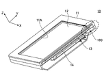
- FIG. 1 is a diagram showing an electronic device 10 including an electrostatic input device 100.
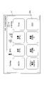
- FIG. 2 is a diagram showing an operation unit of the electronic device 10.
- the XYZ coordinate system will be defined and described.
- the plan view refers to the XY plane view, and the negative Z-axis side is referred to as the lower side or the lower side, and the positive Z-axis direction side is referred to as the upper side or the upper side. It's not a thing.
- the electronic device 10 includes a housing 11 and a panel 12 as main components.
- the housing 11 has a forehead shape in a plan view, and the opening 11A is provided with a panel 12.
- the panel 12 is a cover made of a transparent glass plate or the like.
- a plurality of icons 12A by GUI are displayed on the panel 12, and input is accepted by the user holding a hand on any of the icons 12A of the panel 12. Holding a hand means bringing the hand closer to some extent without touching the panel 12.
- the panel 12 can display the operation units of various devices.
- the operation unit of the air conditioner has eight icons 12A (MODE, temperature UP, air volume UP, Timer, and air conditioner power ON from the upper left to the lower right). / OFF, temperature DOWN, air volume DOWN, ECO (power saving mode)).
- icons 12A MODE, temperature UP, air volume UP, Timer, and air conditioner power ON from the upper left to the lower right.
- / OFF temperature DOWN
- air volume DOWN air volume DOWN
- ECO power saving mode
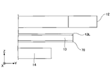
- FIG. 3 is a diagram showing a cross section taken along the line AA of FIG.
- FIG. 3 shows a substrate 13 and an LCD (Liquid Crystal Display) 14 included in the electronic device 10 in addition to the housing 11.
- FIG. 4 is an enlarged view showing a portion surrounded by a broken line ellipse in FIG.
- a substrate 13 and an LCD 14 made of a transparent acrylic plate are arranged on the back side of the panel 12.
- a conductive layer 13L is provided on the upper surface of the substrate 13, and an active shield electrode 70 is provided on the lower surface of the substrate 13.
- FIG. 5 is a diagram showing an input unit 100A of the electrostatic input device 100.
- FIG. 6 is an enlarged view showing a part of FIG. 5.
- the electrostatic input device 100 is an input device that detects the capacitance by a self-capacitance type.
- the input unit 100A includes a substrate 13, eight first detection electrodes 111 to 118, eight first connection electrodes 121 to 128, eight first wirings 131 to 138, and eight first noise canceling wirings.
- the input unit 100A also includes the active shield electrode 70 shown in FIG. 4, but is omitted in FIG.
- connection electrodes 161 to 165, the second wirings 171 to 175, the second noise canceling wires 181 to 185, and the second widening portions 181A to 185A are realized by the conductive layer 13L on the upper surface of the substrate 13.
- the first detection electrodes 111 to 118, the first connection electrodes 121 to 128, the first widening portions 141A to 148A, the second detection electrodes 151 to 155, the second connection electrodes 161 to 165, and the second widening portions 181A to 185A are It is provided in a region overlapping the LCD 14 in a plan view, and is realized by a transparent electrode such as ITO (Indium Tin Oxide).
- the first detection electrodes 111 to 118 and the second detection electrodes 151 to 155 are provided in the region 13A which is a part of the range overlapping the LCD in a plan view.
- the two noise canceling wires 181 to 185 and the second widening portions 181A to 185A are arranged outside the region 13A.
- the two noise canceling wires 181 to 185 and the second widening portions 181A to 185A may be made of ITO.
- the electrostatic input device 100 is an input device that detects the approach of the user's hand to the panel 12 with the second detection electrodes 151 to 155 and detects the operation to the icon 12A with the first detection electrodes 111 to 118.
- the range that can be detected by the first detection electrodes 111 to 118 is within about 3 cm to about 5 cm as an example from the surface of the panel 12 (see FIGS. 1 to 3). Further, the range that can be detected by the second detection electrodes 151 to 155 is within about 10 cm as an example from the surface of the panel 12.
- the surface of the panel 12 is an example of a detection surface.
- the distance from the surface of the panel 12 representing the range detectable by the first detection electrodes 111 to 118 is an example of the first distance, and is from the surface of the panel 12 representing the range detectable by the second detection electrodes 151 to 155.
- the distance is an example of the second distance.
- the second distance is longer than the first distance.
- the electrostatic input device 100 detects an approach within about 10 cm from the surface of the panel 12 of the user's hand with the second detection electrodes 151 to 155, and about 3 cm to about 3 cm from the surface of the panel 12 with the first detection electrodes 111 to 118. Detects an approach within about 5 cm. For example, when the electronic device 10 including the electrostatic input device 100 turns off the display of the LCD 14, and the second detection electrodes 151 to 155 detect the approach of the user's hand to the panel 12, the LCD 14 is turned on. Then, an image as shown in FIG. 2 is displayed, and when an approach to any of the first detection electrodes 111 to 118 is detected, the first detection electrode (one of 111 to 118) that detects the approach is detected.
- the operation of the icon 12A corresponding to the above is accepted, and the electronic device 10 executes a function corresponding to the operated icon 12A (for example, air volume adjustment and temperature adjustment of the air conditioner).
- a function corresponding to the operated icon 12A for example, air volume adjustment and temperature adjustment of the air conditioner.
- the time may be displayed on the LCD 14.
- the LCD 14 may be turned off when the second detection electrodes 151 to 155 do not detect the approach of the user's hand to the panel 12. This is to reduce power consumption by turning on the LCD 14 only when the hand approaches the panel 12.
- the first detection electrodes 111 to 118 are arranged in 4 columns in the X direction and 2 rows in the Y direction in the region 13A, and are arranged at equal intervals in the X direction and the Y direction. More specifically, the first detection electrodes 111 to 114 are arranged from the ⁇ X direction to the + X direction in the row on the + Y direction side, and the first detection electrode 111 to 114 is arranged in the row on the ⁇ Y direction side from the ⁇ X direction to the + X direction. 115 to 118 are arranged. The positions of the first detection electrodes 111 to 118 correspond to the positions of the eight icons 12A shown in FIG. Second detection electrodes 151 to 155 are provided between the first detection electrodes 111 and 118.
- the first detection electrodes 111 to 118 are, as an example, rectangular electrodes having a longitudinal direction in the Y direction, and the first connection electrodes 121 to 128 are connected to each other.
- the first connection electrodes 121 to 128 connect the first detection electrodes 111 to 118 and the first wiring 131 to 138, respectively.
- the first connection electrodes 121 to 128 are provided on the upper surface of the substrate 13 outside the region 13A.
- the first connection electrode 121 is connected to the first detection electrode 111 and extends in the ⁇ X direction.
- the first connection electrode 121 is connected to the end in the ⁇ Y direction of the side on the ⁇ X direction side of the first detection electrode 111.
- the first connection electrode 122 is connected to the first detection electrode 112 and extends in the + Y direction.
- the first connection electrode 122 is connected to the end in the ⁇ X direction of the side on the + Y direction side of the first detection electrode 112.
- the first connection electrode 123 is connected to the first detection electrode 113 and extends in the + Y direction.
- the first connection electrode 123 is connected to the + X direction end of the + Y direction side of the first detection electrode 113.
- the first connection electrode 124 is connected to the first detection electrode 114 and extends in the + X direction.
- the first connection electrode 124 is connected to the end in the ⁇ Y direction of the side on the + X direction side of the first detection electrode 114.
- the first connection electrode 125 is connected to the first detection electrode 115 and extends in the ⁇ Y direction.
- the first connection electrode 125 is connected to the + X direction end of the side of the first detection electrode 115 on the ⁇ Y direction side.
- the first connection electrode 126 is connected to the first detection electrode 116 and extends in the ⁇ Y direction.
- the first connection electrode 126 is connected to the + X direction end of the side of the first detection electrode 116 on the ⁇ Y direction side.
- the first connection electrode 127 is connected to the first detection electrode 117 and extends in the ⁇ Y direction.
- the first connection electrode 127 is connected to the end in the ⁇ X direction of the side on the ⁇ Y direction side of the first detection electrode 117.
- the first connection electrode 128 is connected to the first detection electrode 118 and extends in the ⁇ Y direction.
- the first connection electrode 128 is connected to the end in the ⁇ X direction of the side on the ⁇ Y direction side of the first detection electrode 118.
- the first connection electrodes 125 to 128 close to the convex portion 13B for the terminals of the substrate 13 are the smallest, and the first connection electrodes 122 and 123 farthest from the convex portion 13B. Is the largest, and the size of the first connection electrodes 121 and 124 located between the first connection electrodes 122 and 123 and the first connection electrodes 125 to 128 at a distance from the convex portion 13B is an intermediate size. .. The reason for this will be described later.
- the first wirings 131 to 138 are connected to the first connection electrodes 121 to 128, respectively, and extend along the edge of the substrate 13 outside the region 13A on the upper surface of the substrate 13.
- the first wirings 131 to 138 form eight sets with the first noise canceling wirings 141 to 148, respectively. More specifically, the first wiring 131 and the first noise canceling wiring 141 form the first set, and this also applies to the first wiring 132 to 138 and the first noise canceling wiring 142 to 148. It is the 8th pair from the 1st to the 8th.
- the eighth set includes the first wiring 138 and the first noise canceling wiring 148.
- the first wirings 131 to 138 and the first noise canceling wirings 141 to 148 are located on the same surface because they are included in the conductive layer 13L on the upper surface of the substrate 13, and the first wirings (of 131 to 138) of each set are located on the same surface. 1) and the first noise canceling wiring (one of 141 to 148) are wired next to each other. For example, as shown in FIG. 6, the first wiring 138 extends along the first noise canceling wiring 148 next to the first noise canceling wiring 148.
- the first wirings 131 to 138 are connected to the first detection electrodes 111 to 118 via the first connection electrodes 121 to 128, respectively.
- the first detection electrodes 111 to 118, the first connection electrodes 121 to 128, and the first wiring 131 to 138 are insulated from the first noise canceling wiring 141 to 148, and the second detection electrodes 151 to 155 and the first are the first.
- the two connection electrodes 161 to 165, the second wirings 171 to 175, and the second noise canceling wires 181 to 185 are also insulated.
- the first noise canceling wires 141 to 148 extend along the first wirings 131 to 138 on the outside of the region 13A on the upper surface of the substrate 13, respectively.
- the first noise canceling wires 141 to 148 are provided for the control unit, which will be described later, to acquire the noise used when canceling the noise generated in the first wirings 131 to 138.
- the first widening portions 141A to 148A are connected to the ends of the first noise canceling wires 141 to 148 on the first detection electrodes 111 to 118 side, respectively.
- the first noise canceling wires 141 to 148 extend from the first widening portions 141A to 148A along the first wirings 131 to 138 toward the convex portion 13B of the substrate 13, respectively.
- the first noise canceling wires 141 to 148 and the first wirings 131 to 138 have the same line width and thickness, and the lengths of the first noise canceling wires 141 to 148 are aligned with the lengths of the first wirings 131 to 138. There is.
- the uniform length means that the lengths are the same, or the lengths are different to the extent that noise cancellation is not affected even if they are not exactly the same due to structural restrictions or the like. That means. Further, if there is a hand or the like around the panel, the capacitance changes in the wiring 131 to 138 portion, but the first noise canceling wiring 141 to 148 also changes the capacitance to the same extent, so that the capacitance can be offset.
- the first widening portions 141A to 148A are arranged next to the first connection electrodes 121 to 128, respectively.
- the first widening portions 141A to 148A are provided for the control unit described later to acquire noise used when canceling the noise generated in the first connection electrodes 121 to 128, respectively.
- the first widening portions 141A to 148A each have a line width wider than that of the first noise canceling wiring 141 to 148.
- the line width is the width with respect to the direction in which the first noise canceling wires 141 to 148 extend in a plan view.
- the line widths of the first widening portions 141A to 148A are, for example, equal to the line widths of the first connection electrodes 121 to 128, respectively.
- Such first widening portions 141A to 148A each acquire the same level of noise as the noise acquired by the first connection electrodes 121 to 128.
- the first noise canceling wires 141 to 148 are provided in order to cancel the noise generated in the first wirings 131 to 138, and the first noise canceling wires 141 to 148 are provided in order to cancel the noise generated in the first connection electrodes 121 to 128, respectively.
- a mode in which the widening portions 141A to 148A are provided will be described, but the noises of the first wirings 131 to 138 and the first connection electrodes 121 to 128 connected to each other are combined with the first noise canceling wirings 141 to 148 connected to each other.
- the first widening portions 141A to 148A may be configured to cancel each of them.
- the second detection electrodes 151 to 155 are provided between the eight first detection electrodes 111 to 118 in the region 13A. This is to reduce the size of the electrostatic input device 100.
- the second detection electrode 151 includes an end edge extending in the Y direction on the + X direction side of the first detection electrode 111, an end edge extending in the X direction on the ⁇ Y direction side, and the first detection electrodes 112 and 115. It extends in an L shape between them.
- the second detection electrode 152 includes an end edge extending in the Y direction on the ⁇ X direction side of the first detection electrode 116, an end edge extending in the X direction on the + Y direction side, and the first detection electrodes 112 and 115. It extends in an L shape between them.
- the second detection electrode 153 extends in a cross shape between the first detection electrodes 112, 113, 116, and 117.
- the second detection electrode 154 includes an end edge extending in the Y direction on the + X direction side of the first detection electrode 117, an end edge extending in the X direction on the + Y direction side, and the first detection electrodes 113 and 118. It extends in an L-shape between them.
- the second detection electrode 155 has an end extending in the Y direction on the ⁇ X direction side of the first detection electrode 114, an end extending in the X direction on the ⁇ Y direction side, and the first detection electrodes 113 and 118. It extends in an L-shape between and.
- the second connection electrodes 161 to 165 are connected to the second detection electrodes 151 to 155, respectively.
- the second connection electrodes 161 to 165 connect the second detection electrodes 151 to 155 and the second wirings 171 to 175, respectively.
- the second connection electrodes 161 to 165 are provided on the upper surface of the substrate 13 outside the region 13A.
- the second connection electrode 161 is connected to a position closest to the convex portion 13B through the outside of the region 13A among the portions of the second detection electrode 151 in contact with the region 13A. Therefore, the position where the second connection electrode 161 is connected to the second detection electrode 151 is next to the end on the + Y direction side of the end side extending in the Y direction on the ⁇ X direction side of the first detection electrode 115. be.
- the second wiring 171 is connected to the second connection electrode 161.
- the second connection electrode 162 is connected to a position closest to the convex portion 13B through the outside of the region 13A among the portions of the second detection electrode 152 in contact with the region 13A. Therefore, the position where the second connection electrode 162 is connected to the second detection electrode 152 is next to the end on the ⁇ X direction side of the end edge extending in the X direction on the ⁇ Y direction side of the first detection electrode 116. Is.
- the second wiring 172 is connected to the second connection electrode 162.
- the second connection electrode 163 is connected to a position closest to the convex portion 13B through the outside of the region 13A among the portions of the second detection electrode 153 in contact with the region 13A. Therefore, the position where the second connection electrode 163 is connected to the second detection electrode 152 is at the center of the line width in the X direction of the end portion of the cross-shaped second connection electrode 163 on the ⁇ Y direction side in a plan view. be.
- the second wiring 173 is connected to the second connection electrode 163.
- the second connection electrode 164 is connected to a position closest to the convex portion 13B through the outside of the region 13A among the portions of the second detection electrode 154 in contact with the region 13A. Therefore, the position where the second connection electrode 164 is connected to the second detection electrode 154 is next to the end on the ⁇ X direction side of the end edge extending in the X direction on the ⁇ Y direction side of the first detection electrode 117. Is.
- the second wiring 174 is connected to the second connection electrode 164.
- the second connection electrode 165 is connected to a position closest to the convex portion 13B through the outside of the region 13A among the portions of the second detection electrode 155 in contact with the region 13A. Therefore, the position where the second connection electrode 165 is connected to the second detection electrode 155 is next to the end on the + Y direction side of the end edge extending in the Y direction on the + X direction side of the first detection electrode 118. ..
- the second wiring 175 is connected to the second connection electrode 165.
- the second wirings 171 to 175 are connected to the second connection electrodes 161 to 165, respectively, and extend along the edge of the substrate 13 outside the region 13A on the upper surface of the substrate 13.
- the second wirings 171 to 175 form five sets with the second noise canceling wirings 181 to 185, respectively.
- the second wiring 171 and the second noise canceling wiring 181 form the first set
- the second wirings 172 to 175 and the second noise canceling wirings 182 to 185 are the second, respectively. It is the fifth group from the group.
- the fifth set includes the second wiring 175 and the second noise canceling wiring 185.
- the second wirings 171 to 175 and the second noise canceling wirings 181 to 185 are located on the same surface because they are included in the conductive layer 13L on the upper surface of the substrate 13, and the second wirings (of 171 to 175) of each set are located on the same surface. 1) and the second noise canceling wiring (one of 181 to 185) are wired next to each other.
- the second wiring 174 extends along the second noise canceling wiring 184 next to the second noise canceling wiring 184
- the second wiring 175 extends along the second noise canceling wiring 184.
- Next to 185 it extends along the second noise canceling wire 185.
- the second wirings 171 to 175 are connected to the second detection electrodes 151 to 155 via the second connection electrodes 161 to 165, respectively.
- the second detection electrodes 151 to 155, the second connection electrodes 161 to 165, and the second wirings 171 to 175 are insulated from the second noise canceling wires 181 to 185, and the first detection electrodes 111 to 118 and the first are
- the 1 connection electrodes 121 to 128, the first wiring 131 to 138, and the first noise canceling wiring 141 to 148 are also insulated.
- the second noise canceling wirings 181 to 185 extend along the second wirings 171 to 175 on the outside of the region 13A on the upper surface of the substrate 13, respectively.
- the second noise canceling wires 181 to 185 are provided for the control unit, which will be described later, to acquire the noise used when canceling the noise generated in the second wirings 171 to 175.
- the second widening portions 181A to 185A are connected to the ends of the second noise canceling wires 181 to 185 on the second detection electrodes 151 to 155 side, respectively.
- the second noise canceling wires 181 to 185 extend from the second widening portions 181A to 185A toward the convex portions 13B of the substrate 13 along the second wirings 171 to 175, respectively.
- the second noise canceling wires 181 to 185 and the second wirings 171 to 175 have the same line width and thickness, and the lengths of the second noise canceling wires 181 to 185 are aligned with the lengths of the second wirings 171 to 175. There is.
- the uniform length means that the lengths are the same, or the lengths are different to the extent that noise cancellation is not affected even if they are not exactly the same due to structural restrictions or the like. That means.
- the second widening portions 181A to 185A are arranged next to the second connection electrodes 161 to 165, respectively.
- the second widening portions 181A to 185A are provided for the control unit, which will be described later, to acquire noise used when canceling the noise generated in the second connection electrodes 161 to 165, respectively.
- the second widening portions 181A to 185A each have a line width wider than that of the second noise canceling wires 181 to 185.
- the line width is the width with respect to the direction in which the second noise canceling wires 181 to 185 extend in a plan view.
- the line widths of the second widening portions 181A to 185A are, for example, equal to the line widths of the second connection electrodes 161 to 165, respectively.
- Such second widening portions 181A to 185A each acquire the same level of noise as the noise acquired by the second connection electrodes 161 to 165.
- the second noise canceling wires 181 to 185 are provided to cancel the noise generated in the second wirings 171 to 175, respectively, and the second noise canceling wires 181 to 185 are provided to cancel the noise generated in the second connection electrodes 161 to 165, respectively.
- a mode in which the widening portions 181A to 185A are provided will be described, but the noises of the second wirings 171 to 175 and the second connection electrodes 161 to 165 connected to each other are combined with each other by the second noise canceling wires 181 to 185 and the second noise canceling wires 181 to 185.
- the second widening portions 181A to 185A may be configured to cancel each of them.
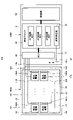
- FIG. 7 is a diagram showing the configuration of the electrostatic input device 100.
- the electrostatic input device 100 includes an input unit 100A and a detection circuit 100B.
- the input unit 100A has the configuration shown in FIG. 5, but is simplified in FIG. 7.
- the first detection electrodes 111 to 118, the first wiring 131 to 138, the first noise canceling wiring 141 to 148, the first widening unit 141A to 148A, and the second detection electrode are shown.
- 151 to 155, the second wiring 171 and 175, the second noise canceling wiring 181 and 185, and the second widening portion 181A to 185A are shown.
- FIG. 7 schematically shows each wiring included in the input unit 100A.
- the offset wirings 181 to 185 and the second widening portions 181A to 185A are arranged above the active shield electrode 70.
- the first connection electrodes 121 to 128 and the second connection electrodes 161 to 165, which are omitted in FIG. 7, are also arranged above the active shield electrode 70.
- the second wirings 171 to 175 are connected by the detection circuit 100B, and one wiring 191 is connected to the MUX 20.
- the second noise canceling wirings 181 to 185 are connected by the detection circuit 100B, and one wiring 192 is connected to the MUX.
- the detection circuit 100B includes a MUX (multiplexer) 20, a measurement block 30, and a control unit 50.
- the input side of the MUX 20 is connected to the first detection electrodes 111 to 118 via the first wiring 131 to 138, and is also connected to the first noise canceling wiring 141 to 148.
- the second detection electrodes 151 to 155 are connected to the MUX 20 via the second wirings 171 to 175 and the wiring 191.
- the second noise canceling wirings 181 to 185 are connected to the MUX 20 via the wiring 192.
- the output side of the MUX 20 is connected to the measurement block 30.
- the measurement block 30 has the capacitances of the first detection electrodes 111 to 118, the capacitance of the first noise canceling wires 141 to 148 combined, the capacitances of the second detection electrodes 151 to 155, and the second noise.
- the connection between the input side and the output side is switched in chronological order.
- the measurement block 30 has 16 measurement units 31 and one waveform generator 32.
- Each measuring unit 31 includes an AFE circuit and an ADC (Analog to Digital Converter).
- the 16 measuring units perform signal adjustment and AD conversion to the capacitances of the first detection electrodes 111 to 118 and the capacitances of the first noise canceling wires 141 to 148, respectively, to the control unit 50.
- Output Further, in the second sequence, signal adjustment and AD conversion are performed on the capacitance of the second detection electrodes 151 to 155 and the capacitance of the second noise canceling wires 181 to 185, respectively, to the control unit 50. Output.
- the capacitances of the first detection electrodes 111 to 118 are the capacitances measured via the first connection electrodes 121 to 128 and the first wiring 131 to 138, respectively, and are the capacitances measured through the first connection electrodes 121 to 121. Includes capacitance at 128 and first wiring 131-138.
- the combined capacitance of the second detection electrodes 151 to 155 is the capacitance measured via the second connection electrodes 161 to 165 and the second wirings 171 to 175, respectively, and the second connection electrode 161 Includes capacitance at ⁇ 165 and second wirings 171-175.
- the waveform generator 32 is connected to the active shield electrode 70 via the wiring 71, and an AC signal as an active shield signal is applied to the active shield electrode 70.
- the active shield electrode 70 includes first detection electrodes 111 to 118, first connection electrodes 121 to 128, first wiring 131 to 138, first noise canceling wiring 141 to 148, second detection electrodes 151 to 155, and second connection electrode. 161 to 165, second wirings 171 to 175, and second noise canceling wirings 181 to 185 are provided to shield the second wirings 181 to 185 from noise of the LCD 14.
- the control unit 50 calculates and outputs a difference value between each capacitance of the first detection electrodes 111 to 118 and a predetermined reference value.
- the control unit 50 performs the following processing on the measured value of the capacitance of the first detection electrodes 111 to 118 input from the measurement block 30.
- the control unit 50 obtains the average value of the measured values of the capacitance obtained by measuring a plurality of times in time series. Then, the control unit 50 acquires the obtained average value as a reference value when the first detection electrodes 111 to 118 measure the capacitance.
- the control unit 50 subtracts a reference value from the measured value of the capacitance of the first detection electrodes 111 to 118, and the difference value of the capacitance according to the distance between the first detection electrodes 111 to 118 and the hand. Ask for.
- the control unit 50 also has the capacitances of the first noise canceling wires 141 to 148, the capacitance of the second detection electrodes 151 to 155 combined, and the capacitance of the second noise canceling wires 181 to 185 combined.
- the same processing as the capacitance of the first detection electrodes 111 to 118 is performed, and the capacitance of the first noise canceling wires 141 to 148, the combined capacitance of the second detection electrodes 151 to 155, and the second noise cancellation are performed.
- the difference value (hereinafter referred to as a difference value) of the total capacitance of the wirings 181 to 185 is obtained. Each difference value becomes a value according to the distance between the hand and the panel 12.
- control unit 50 subtracts the difference values calculated for the first noise canceling wires 141 to 148 from the difference values calculated for the first detection electrodes 111 to 118, respectively, so that the first connection electrodes 121 to 128 and the first connection electrode 50 are the first.
- the noise component included in the difference value calculated for the wirings 131 to 138 is canceled.
- control unit 50 subtracts the difference value calculated for the combined capacitance of the second noise canceling wires 181 to 185 from the difference value calculated for the combined capacitance of the second detection electrodes 151 to 155. Cancels the noise component included in the difference value calculated for the combined capacitance of the second connection electrodes 161 to 165 and the second wirings 171 to 175.
- FIG. 8 is a diagram illustrating noise cancellation at the second detection electrode 151.
- the second detection electrode 151, the second connection electrode 161 and the resistor R1 corresponding to the second wiring 171, the resistor R2 corresponding to the active shield electrode 70, the LCD 14, and the second noise canceling wiring are shown.
- 181 and resistors Rs corresponding to the second widening portion 181A are shown.
- the capacitance between the resistor R1 corresponding to the second detection electrode 151, the second connection electrode 161 and the second wiring 171 and the resistor R2 corresponding to the active shield electrode 70 is indicated by the capacitor Crs1.
- the capacitor Crs1 is mainly the capacitance between the second detection electrode 151 and the active shield electrode 70.
- the capacitance between the resistor R2 corresponding to the active shield electrode 70 and the LCD 14 is indicated by the capacitor Csg.
- the capacitance between the second noise canceling wiring 181 and the second widening portion 181A and the active shield electrode 70 is indicated by the capacitor Crs2.
- the combined area of the second detection electrode 151, the second connection electrode 161 and the second wiring 171 is different from the combined area of the second noise canceling wiring 181 and the second widening portion 181A. Therefore, a capacitor is added to make the capacitances of the capacitor Crs1 and the capacitor Crs2 equal.
- noise applied to a wide range propagates to the active shield electrode 70 through the capacitor Csg as shown by the broken line arrow, and further propagates to the second detection electrode 151 and the second connection through the capacitor Crs1. It propagates to the electrode 161 and the second wiring 171.
- the noise generated in the LCD 14 propagates to the active shield electrode 70 through the capacitor Cgs, and further propagates to the second noise canceling wiring 181 and the second widening portion 181A through the capacitor Crs2. Therefore, the lengths of the second wiring 171 and the second noise canceling wiring 181 are aligned to align the time constants, and the second connection electrode 161 and the second widening portion 181A can acquire the same level of noise.
- the control unit 50 subtracts the difference value calculated for the second noise canceling wiring 181 and the second widening unit 181A from the difference value calculated for the second detection electrode 151, the second connection electrode 161 and the second wiring 171. Thereby, the influence of the noise on the second connection electrode 161 and the second wiring 171 can be canceled from the difference values calculated for the second detection electrode 151, the second connection electrode 161 and the second wiring 171. Since the equivalent circuit as shown in FIG. 8 also exists for the second detection electrodes 152 to 155, the control unit 50 has the second detection electrodes 152 to 155, the second connection electrodes 162 to 165, and the second detection electrode 152 to 155. From the difference values calculated for the two wirings 172 to 175, the influence of noise on the second connection electrodes 162 to 165 and the second wirings 172 to 175 can be canceled.
- the region where the second detection electrodes 151 to 155 exist is relatively wide, if one detection electrode is used, the distribution of resistance and capacitance is widened, and the second detection electrodes 151 to 155 and the second noise canceling wiring 181 to 185 are used. It becomes difficult to match the phase difference. By dividing the second detection electrodes 151 to 155, it becomes easy to match the phase difference between the second detection electrodes 151 to 155 and the second noise canceling wirings 181 to 185, and the noise can be easily canceled.
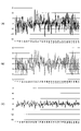
- FIG. 9 is a diagram illustrating a difference value in which the noise calculated for the first detection electrode 111 is canceled.
- FIG. 9A shows the difference value calculated by the control unit 50 for the first detection electrode 111
- FIG. 9B shows the difference value calculated by the control unit 50 for the first noise canceling wiring 141 and the first widening unit 141A. The difference value is shown
- FIG. 9 (C) shows the result of subtracting the difference value of FIG. 9 (B) from the difference value of FIG. 9 (A).
- the difference value shown in FIG. 9A is obtained by subtracting the reference value from the total capacitance of the capacitance of the first detection electrode 111 and the capacitance of the first connection electrode 121 and the first wiring 131. It is a value to be obtained, and includes a noise component acquired by the first detection electrode 111, the first connection electrode 121, and the first wiring 131.
- the difference value shown in FIG. 9B is a value obtained by subtracting the reference value from the capacitance of the first noise canceling wiring 141 and the first widening portion 141A.
- the difference value shown in FIG. 9 (C) obtained by subtracting the difference value in FIG. 9 (B) from the difference value in FIG. 9 (A) is based on the capacitance obtained only by the first detection electrode 111. Represents the difference value obtained by subtracting the value.
- the difference value obtained only by the first detection electrode 111 can be obtained with high accuracy. It should be noted that such a highly accurate difference value can be similarly obtained for the first detection electrodes 112 to 118.
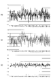
- FIG. 10 is a diagram for explaining the difference value in which the noise calculated for the second detection electrodes 151 to 155 is canceled.
- the control unit 50 shows the difference value in which the second detection electrodes 151 to 155 are combined
- the control unit 50 shows the second noise canceling wirings 181 to 185 and the second widening unit.
- the total difference value of 181A to 185A is shown
- FIG. 10C shows the result of subtracting the difference value of FIG. 10B from the difference value of FIG. 10A.
- the difference value shown in FIG. 10A is based on the total capacitance of the second detection electrodes 151 to 155 and the capacitances of the second connection electrodes 161 to 165 and the second wiring 171 to 175. It is a value obtained by subtracting the reference value, and includes noise components acquired by the second detection electrodes 151 to 155, the second connection electrodes 161 to 165, and the second wiring 171 to 175.
- the difference value shown in FIG. 10B is a value obtained by subtracting the reference value from the capacitances of the second noise canceling wires 181 to 185 and the second widening portions 181A to 185A.
- the second detection electrodes 151 to 155 are not divided, one large detection electrode including the second detection electrodes 151 to 155 is used.
- the detection electrode is large, the variation in the length of the path from an arbitrary point of the detection electrode to the connection electrode becomes large.
- the detection electrode uses a transparent electrode, the resistance value is high and the influence of the path length is large.
- the difference in the length of the path from any point of the second detection electrodes 151 to 155 to the second connection electrodes 161 to 165 becomes small.
- the second noise canceling wires 181 to 185 and the second widening portions 181A to 185A for canceling the noise are provided, the noise can be canceled.
- the second detection electrodes 151 to 155 are provided between the eight first detection electrodes 111 to 118 in the region 13A. Therefore, the electrostatic input device 100 can be miniaturized.
- the second detection electrodes 151 to 155 divided into five are included as detection electrodes for detecting the proximity of the hand, and the second noise canceling wires 181 to 185 and the second widening portion 181A to cancel the noise.
- 185A was provided.
- the lengths of the second noise canceling wires 181 to 185 are aligned with the lengths of the second wirings 171 to 175, and the time constants of the second noise canceling wires 181 to 185 are aligned with the time constants of the second wirings 171 to 175.
- the phase of the noise acquired by the second noise canceling wirings 181 to 185 can be aligned with the phase of the noise acquired by the second wirings 171 to 175. Therefore, it is possible to cancel the noise acquired by the second noise canceling wirings 181 to 185 and the noise acquired by the second wirings 171 to 175. Further, since the second widening portions 181A to 185A can acquire the same level of noise as the noise acquired by the second connection electrodes 161 to 165, the noise acquired by the second connection electrodes 161 to 165 and the second widening are widened. It is possible to cancel out the noise acquired by the units 181A to 185A.
- the difference value obtained only by each of the second detection electrodes 151 to 155 can be obtained with high accuracy, and the proximity of the hand can be detected with high accuracy. Further, since the second detection electrodes 151 to 155 divided into five have a relatively small distribution constant and are not easily affected by noise, the second detection electrode with respect to the phase of the difference value obtained for the first detection electrodes 111 to 118 It is possible to minimize the phase delay of the difference values obtained for 151 to 155.
- the hand approaches the second wiring 171 to 175, a capacitance is formed between the second wiring 171 to 175 and the hand, and the difference value obtained via the second wiring 171 to 175 changes. Since the second noise canceling wirings 181 to 185 are arranged next to the second wirings 171 to 175, the change in the difference value when the hands approach the second wirings 171 to 175 is the second noise canceling wirings 181 to 185. It can be offset by the difference value obtained through. Therefore, the approach of the hand to the second detection electrodes 151 to 155 can be detected with high accuracy.
- the first noise canceling wires 141 to 148 and the first widening portions 141A to 148A are provided in order to cancel the noise.
- the lengths of the first noise canceling wires 141 to 148 are aligned with the lengths of the first wirings 131 to 138, and the time constants of the first noise canceling wires 141 to 148 are the time constants of the first wirings 131 to 138. Therefore, the phase of the noise acquired by the first noise canceling wires 141 to 148 can be aligned with the phase of the noise acquired by the first wirings 131 to 138.
- the noise acquired by the first wirings 131 to 138 can be offset by the noise acquired by the first noise canceling wires 141 to 148, respectively.
- the first widening portions 141A to 148A can acquire the same level of noise as the noise acquired by the first connection electrodes 121 to 128. Thereby, the noise acquired by the first widening portions 141A to 148A and the noise acquired by the first connection electrodes 121 to 128 can be canceled out. Therefore, the difference value obtained only by each of the first detection electrodes 111 to 118 can be obtained with high accuracy. As a result, it is possible to determine with high accuracy which icon 12A was operated in a non-contact manner.
- the hand when the hand approaches the first wiring 131 to 138, a capacitance is formed between the first wiring 131 to 138 and the hand, and the difference value obtained via the first wiring 131 to 138 changes. Since the first noise canceling wires 141 to 148 are arranged next to the first wirings 131 to 138, the change in the difference value when the hand approaches the first wirings 131 to 138 is the change in the first noise canceling wires 141 to 148. It can be offset by the difference value obtained through. Therefore, the approach of the hand to the first detection electrodes 111 to 118 can be detected with high accuracy.
- the electrostatic input device 100 includes the active shield electrode 70 between the LCD 14 and the conductive layer 13L, the noise generated by the LCD 14 is generated by the first detection electrodes 111 to 118 and the first connection electrodes 121 to the conductive layer 13L. 128, 1st wiring 131-138, 1st noise canceling wiring 141-148, 1st widening portion 141A-148A, 2nd detection electrode 151-155, 2nd connection electrode 161-165, 2nd wiring 171-175, 1st 2 It is possible to suppress the influence of the noise canceling wirings 181 to 185 and the second widening portions 181A to 185A.
- the electrostatic input device 100 may be configured not to include the active shield electrode 70.
- the electrostatic input device 100 may be a mutual capacitance type.
- the electrostatic input device 100 includes the second detection electrodes 151 to 155 divided into five as the detection electrodes for detecting the proximity of the hand has been described, but the second detection electrodes 151 to 155 have been described.
- the configuration may include one detection electrode in which the second detection electrodes 151 to 155 are combined into one. In particular, when the phase delay is not a problem, such a configuration may be used.
- FIG. 11 is a diagram showing an input unit 100AM1 of the electrostatic input device of the first modification of the embodiment.
- the input unit 100AM1 includes a non-divided second detection electrode 150 instead of the second detection electrodes 151 to 155 of the input unit 100A shown in FIG. 5, and replaces the second connection electrodes 161 to 165 and the second wirings 171 to 175. Includes two second connection electrodes 161M1 and 162M1 and two second wirings 171M1 and 172M1.
- the input unit 100AM1 includes the second noise canceling wires 181M1 and 182M1 and the second widening units 181AM1 and 182AM1 instead of the second noise canceling wires 181 to 185 and the second widening sections 181A to 185A shown in FIG.
- an electrostatic input device that can be miniaturized (an electrostatic input device including an input unit 100AM1 shown in FIG. 11 instead of the input unit 100A (see FIG. 5) of the electrostatic input device 100).
- FIG. 12 is a diagram showing an input unit 100AM2 of the electrostatic input device of the second modification of the embodiment.
- the input unit 100AM2 includes the second detection electrodes 151M2 to 153M2 divided into three parts in place of the second detection electrodes 151 to 155 of the input unit 100A shown in FIG. 5, and the second connection electrodes 161 to 165 and the second wiring 171 to 175. Instead of, three second connection electrodes 161M2 to 163M2 and three second wirings 171M2 to 173M2 are included.
- the input unit 100AM2 uses three second noise canceling wires 181M2 to 183M2 and a second widening unit 181AM2 to 183AM2 instead of the second noise canceling wires 181 to 185 and the second widening portions 181A to 185A shown in FIG. include.
- the second detection electrode 151M2 has a configuration in which the second detection electrodes 151 and 152 shown in FIG. 5 are combined, and the second detection electrode 152M2 is the same as the second detection electrode 153 shown in FIG. 5, and is the second detection electrode.
- the 153M2 has a configuration in which the second detection electrodes 154 and 155 shown in FIG. 5 are combined.
- the second connection electrode 161M2 corresponds to the second connection electrode 162 shown in FIG. 5
- the second connection electrode 162M2 corresponds to the second connection electrode 163 shown in FIG. 5
- the second connection electrode 163M2 corresponds to FIG. It corresponds to the second connection electrode 164.
- the second wiring 171M2 corresponds to the second wiring 172 shown in FIG. 5, the second wiring 172M2 corresponds to the second wiring 173 shown in FIG. 5, and the second wiring 173M2 corresponds to the second wiring 174 shown in FIG. ..
- the second noise canceling wiring 181M2 corresponds to the second noise canceling wiring 182 shown in FIG. 5, the second noise canceling wiring 182M2 corresponds to the second noise canceling wiring 183 shown in FIG. 5, and the second noise canceling wiring 183M2 corresponds to the figure. It corresponds to the second noise canceling wiring 184 shown in 5.
- the second widening portion 181AM2 corresponds to the second widening portion 182A shown in FIG.
- the second widening portion 182AM2 corresponds to the second widening portion 183A shown in FIG. 5, and the second widening portion 183AM2 corresponds to the second widening portion 183AM2 shown in FIG. It corresponds to the widening portion 184A.
- an electrostatic input device that can be miniaturized (an electrostatic input device including an input unit 100AM2 shown in FIG. 12 instead of the input unit 100A (see FIG. 5) of the electrostatic input device 100).
- noise canceling wiring 141 to 148 and the second noise canceling wiring 181 to 185, 181M1, 182M1, and 181M2 to 183M2 noise can be removed and the detection accuracy can be improved.
Landscapes
- Engineering & Computer Science (AREA)
- General Engineering & Computer Science (AREA)
- Theoretical Computer Science (AREA)
- Human Computer Interaction (AREA)
- Physics & Mathematics (AREA)
- General Physics & Mathematics (AREA)
- Computer Networks & Wireless Communication (AREA)
- Position Input By Displaying (AREA)
Abstract
小形化が可能な静電入力装置を提供する。 静電入力装置は、検出面から第1距離以内の被検出体の接近を検出する複数の第1検出電極と、前記複数の第1検出電極同士の間に設けられ、前記検出面から前記第1距離よりも長い第2距離以内の被検出体の接近を検出する第2検出電極と、前記複数の第1検出電極及び前記第2検出電極の静電容量の変化を検出する検出回路とを含む。
Description
本発明は、静電入力装置に関する。
従来より、表示領域に、検出面での近接または接触を検出することの可能な複数の第1のタッチセンサを備えると共に、額縁領域に、前記検出面への近接または接触を検出することの可能な複数の第2のタッチセンサを備えるタッチパネルがある。前記複数の第1のタッチセンサは、電極に電気的に接続された高抵抗素子を備える、静電容量センサである(例えば、特許文献1参照)。
ところで、従来のタッチパネルは、複数の第2のタッチセンサが第1のタッチセンサが設けられる領域の外側の額縁領域に設けられているため、小形化が困難である。
そこで、小形化が可能な静電入力装置を提供することを目的とする。
本発明の実施形態の静電入力装置は、検出面から第1距離以内の被検出体の接近を検出する複数の第1検出電極と、前記複数の第1検出電極同士の間に設けられ、前記検出面から前記第1距離よりも長い第2距離以内の被検出体の接近を検出する第2検出電極と、前記複数の第1検出電極及び前記第2検出電極の静電容量の変化を検出する検出回路とを含む。
小形化が可能な静電入力装置を提供することができる。
以下、本発明の静電入力装置を適用した実施形態について説明する。
<実施形態>
図1は、静電入力装置100を含む電子機器10を示す図である。図2は、電子機器10の操作部を示す図である。以下では、XYZ座標系を定義して説明する。また、以下では、説明の便宜上、平面視とはXY面視をいい、Z軸負方向側を下側又は下、Z軸正方向側を上側又は上と称すが、普遍的な上下関係を表すものではない。
図1は、静電入力装置100を含む電子機器10を示す図である。図2は、電子機器10の操作部を示す図である。以下では、XYZ座標系を定義して説明する。また、以下では、説明の便宜上、平面視とはXY面視をいい、Z軸負方向側を下側又は下、Z軸正方向側を上側又は上と称すが、普遍的な上下関係を表すものではない。
電子機器10は、主な構成要素として、筐体11、パネル12を含む。筐体11は、平面視で額状であり、開口部11Aにはパネル12が設けられている。パネル12は、透明なガラス板等で構成されるカバーである。パネル12には、図2に示すようにGUI(Graphic User Interface)による複数のアイコン12Aが表示され、利用者がパネル12のいずれかのアイコン12Aに手を翳すことによって入力が受け付けられる。手を翳すとは、パネル12に接触せずにある程度手を近づけることをいう。
パネル12には様々な機器の操作部を表示でき、図2では一例としてエアコンディショナの操作部に8つのアイコン12A(左上から右下にかけて、MODE、温度UP、風量UP、Timer、エアコン電源ON/OFF、温度DOWN、風量DOWN、ECO(省電力モード))を示す。例えば、エアコン電源ON/OFFのアイコン12Aの上に手を翳すと、エアコン電源のON/OFFを切り替えることができる。このような操作の受付は、電子機器10に含まれる静電入力装置100によって行われる。なお、ここでは手を翳すことによって操作を行う形態について説明するが、手でパネル12に触れることによって操作を行うこともできる。
図3は、図1のA-A矢視断面を示す図である。図3には、筐体11に加えて、電子機器10に含まれる基板13及びLCD(Liquid Crystal Display)14を示す。図4は、図3における破線の楕円で囲む部分を拡大して示す図である。図3及び図4に示すように、パネル12の裏側には、透明アクリル板で構成される基板13とLCD14が配置される。基板13の上面には導電レイヤ13Lが設けられており、基板13の下面にはアクティブシールド電極70が設けられている。
図5は、静電入力装置100の入力部100Aを示す図である。図6は、図5の一部分を拡大して示す図である。静電入力装置100は、自己容量式で静電容量を検出する入力装置である。入力部100Aは、基板13と、8つの第1検出電極111~118と、8つの第1接続電極121~128と、8本の第1配線131~138と、8本の第1ノイズ相殺配線141~148と、8つの第1拡幅部141A~148Aと、5つの第2検出電極151~155と、5つの第2接続電極161~165と、5本の第2配線171~175と、5本の第2ノイズ相殺配線181~185と、5つの第2拡幅部181A~185Aとを含む。また、入力部100Aは、図4に示すアクティブシールド電極70も含むが、図5では省略する。
第1検出電極111~118、第1接続電極121~128、第1配線131~138、第1ノイズ相殺配線141~148、第1拡幅部141A~148A、第2検出電極151~155、第2接続電極161~165、第2配線171~175、第2ノイズ相殺配線181~185、及び第2拡幅部181A~185Aは、基板13の上面の導電レイヤ13Lによって実現される。
第1検出電極111~118、第1接続電極121~128、第1拡幅部141A~148A、第2検出電極151~155、第2接続電極161~165、及び第2拡幅部181A~185Aは、平面視でLCD14と重なる領域に設けられ、例えばITO(Indium Tin Oxide)のような透明電極によって実現される。平面視でLCDと重なる範囲の一部分の領域13Aに、第1検出電極111~118、及び第2検出電極151~155が設けられる。また、第1接続電極121~128、第1配線131~138、第1ノイズ相殺配線141~148、第1拡幅部141A~148A、第2接続電極161~165、第2配線171~175、第2ノイズ相殺配線181~185、及び第2拡幅部181A~185Aは、領域13Aの外側に配設される。第1接続電極121~128、第1配線131~138、第1ノイズ相殺配線141~148、第1拡幅部141A~148A、第2接続電極161~165、第2配線171~175、第2ノイズ相殺配線181~185、及び第2拡幅部181A~185Aは、領域13Aの外側に配設されてLCD14とは重ならないため、例えば、銀インクのように非透明な導体で作製されていてもよい。なお、第1接続電極121~128、第1配線131~138、第1ノイズ相殺配線141~148、第1拡幅部141A~148A、第2接続電極161~165、第2配線171~175、第2ノイズ相殺配線181~185、及び第2拡幅部181A~185Aは、ITOで作製されてもよい。
静電入力装置100は、第2検出電極151~155で利用者の手のパネル12への接近を検出し、第1検出電極111~118でアイコン12Aへの操作を検出する入力装置である。第1検出電極111~118で検出可能な範囲は、パネル12(図1乃至図3参照)の表面から一例として約3cm~約5cm以内である。また、第2検出電極151~155で検出可能な範囲は、パネル12の表面から一例として約10cm以内である。パネル12の表面は検出面の一例である。第1検出電極111~118で検出可能な範囲を表すパネル12の表面からの距離は第1距離の一例であり、第2検出電極151~155で検出可能な範囲を表すパネル12の表面からの距離は第2距離の一例である。第2距離は第1距離よりも長い。
静電入力装置100は、第2検出電極151~155で利用者の手のパネル12の表面から約10cm以内の接近を検出し、第1検出電極111~118でパネル12の表面から約3cm~約5cm以内への接近を検出する。例えば、静電入力装置100を含む電子機器10がLCD14の表示をオフにしている状態で、第2検出電極151~155で利用者の手のパネル12への接近が検出されるとLCD14をオンにして図2に示すような画像を表示し、第1検出電極111~118のいずれかへの接近が検出されると、接近を検出した第1検出電極(111~118のいずれか1つ)に対応するアイコン12Aの操作が受け付けられ、電子機器10は操作が行われたアイコン12Aに対応する機能(例えばエアコンディショナの風量調節や温度調節等)を実行する。また、第2検出電極151~155で利用者の手のパネル12への接近が検出されなくなると、LCD14に時刻を表示してもよい。パネル12に手が接近したときにのみアイコン12Aを表示することによって、一つの画面に複数の機能を持たせることができる。または、第2検出電極151~155で利用者の手のパネル12への接近が検出されなくなると、LCD14がオフにしてもよい。パネル12に手が接近したときにのみLCD14をオンにすることによって、消費電力を低減するためである。
第1検出電極111~118は、領域13A内において、X方向に4列、Y方向に2行に配列され、X方向及びY方向に等間隔で配置されている。より具体的には、+Y方向側の行には-X方向から+X方向にかけて第1検出電極111~114が配列され、-Y方向側の行には-X方向から+X方向にかけて第1検出電極115~118が配列されている。第1検出電極111~118の位置は、図2に示す8つのアイコン12Aの位置に対応している。第1検出電極111~118の間には、第2検出電極151~155が設けられている。第1検出電極111~118は、一例としてY方向に長手方向を有する長方形状の電極であり、第1接続電極121~128がそれぞれ接続されている。
第1接続電極121~128は、第1検出電極111~118と、第1配線131~138とをそれぞれ接続している。第1接続電極121~128は、基板13の上面において領域13Aの外側に設けられている。
第1接続電極121は、第1検出電極111と接続され、-X方向に延在している。第1接続電極121は、第1検出電極111の-X方向側の辺の-Y方向の端に接続される。第1接続電極122は、第1検出電極112と接続され、+Y方向に延在している。第1接続電極122は、第1検出電極112の+Y方向側の辺の-X方向の端に接続される。第1接続電極123は、第1検出電極113と接続され、+Y方向に延在している。第1接続電極123は、第1検出電極113の+Y方向側の辺の+X方向の端に接続される。第1接続電極124は、第1検出電極114と接続され、+X方向に延在している。第1接続電極124は、第1検出電極114の+X方向側の辺の-Y方向の端に接続される。
第1接続電極125は、第1検出電極115と接続され、-Y方向に延在している。第1接続電極125は、第1検出電極115の-Y方向側の辺の+X方向の端に接続される。第1接続電極126は、第1検出電極116と接続され、-Y方向に延在している。第1接続電極126は、第1検出電極116の-Y方向側の辺の+X方向の端に接続される。第1接続電極127は、第1検出電極117と接続され、-Y方向に延在している。第1接続電極127は、第1検出電極117の-Y方向側の辺の-X方向の端に接続される。第1接続電極128は、第1検出電極118と接続され、-Y方向に延在している。第1接続電極128は、第1検出電極118の-Y方向側の辺の-X方向の端に接続される。
第1接続電極121~128の平面視でのサイズは、基板13の端子用の凸部13Bに近い第1接続電極125~128が最も小さく、凸部13Bから最も遠い第1接続電極122及び123が最も大きく、凸部13Bからの距離が第1接続電極122及び123と、第1接続電極125~128との間にある第1接続電極121及び124のサイズが中間的なサイズになっている。この理由については後述する。
第1配線131~138は、第1接続電極121~128にそれぞれ接続され、基板13の上面の領域13Aの外側において、基板13の縁に沿って延在している。第1配線131~138は、それぞれ、第1ノイズ相殺配線141~148と8つの組をなしている。より具体的には、第1配線131と第1ノイズ相殺配線141は1つ目の組をなしており、これは第1配線132~138と第1ノイズ相殺配線142~148についても同様に2つ目から8つ目の組をなしている。8つ目の組は、第1配線138と第1ノイズ相殺配線148を含む。
第1配線131~138と第1ノイズ相殺配線141~148は、基板13の上面の導電レイヤ13Lに含まれるため同一面上に位置しており、各組の第1配線(131~138のうちの1つ)と第1ノイズ相殺配線(141~148のうちの1つ)とは隣り合って配線されている。例えば、図6に示すように、第1配線138は、第1ノイズ相殺配線148の隣で第1ノイズ相殺配線148に沿って延在している。
第1配線131~138は、第1接続電極121~128を介して第1検出電極111~118にそれぞれ接続されている。第1検出電極111~118、第1接続電極121~128、及び第1配線131~138は、第1ノイズ相殺配線141~148とは絶縁されているとともに、第2検出電極151~155、第2接続電極161~165、第2配線171~175、及び第2ノイズ相殺配線181~185とも絶縁されている。
第1ノイズ相殺配線141~148は、基板13の上面の領域13Aの外側において、第1配線131~138に沿ってそれぞれ延在している。第1ノイズ相殺配線141~148は、後述する制御部が、第1配線131~138に生じるノイズをキャンセルする際に利用するノイズを取得するために設けられている。
第1ノイズ相殺配線141~148の第1検出電極111~118側の端部には第1拡幅部141A~148Aがそれぞれ接続されている。第1ノイズ相殺配線141~148は、それぞれ、第1拡幅部141A~148Aから第1配線131~138に沿って基板13の凸部13Bに向かって延在している。第1ノイズ相殺配線141~148と第1配線131~138は、線幅及び厚さが等しく、第1ノイズ相殺配線141~148の長さは、第1配線131~138の長さと揃えられている。第1ノイズ相殺配線141~148と第1配線131~138とが受けるノイズを揃えるためである。長さが揃えられているとは、長さが同一であるか、又は、構造上の制約等によって厳密には同一ではなくてもノイズのキャンセルに影響が生じない程度の長さの差であることをいう。また、パネル周囲に手などがあると、配線131~138部分で静電容量が変化するが、第1ノイズ相殺配線141~148も同程度に静電容量が変化するので、相殺できる。
第1拡幅部141A~148Aは、それぞれ、第1接続電極121~128の隣に配置されている。第1拡幅部141A~148Aは、後述する制御部が、第1接続電極121~128に生じるノイズをそれぞれキャンセルする際に利用するノイズを取得するために設けられている。第1拡幅部141A~148Aは、それぞれ第1ノイズ相殺配線141~148よりも広い線幅を有する。線幅とは、平面視で第1ノイズ相殺配線141~148が延在する方向に対する幅である。第1拡幅部141A~148Aの線幅は、一例として第1接続電極121~128の線幅とそれぞれ等しい。このような第1拡幅部141A~148Aは、それぞれ、第1接続電極121~128が取得するノイズと同レベルのノイズを取得する。
なお、ここでは、第1配線131~138に生じるノイズをそれぞれキャンセルするために第1ノイズ相殺配線141~148を設けるとともに、第1接続電極121~128に生じるノイズをそれぞれキャンセルするために第1拡幅部141A~148Aを設ける形態について説明するが、互いに接続される第1配線131~138及び第1接続電極121~128のそれぞれのノイズを、互いに接続される第1ノイズ相殺配線141~148及び第1拡幅部141A~148Aでそれぞれキャンセルする構成であってもよい。
第2検出電極151~155は、領域13A内において8つの第1検出電極111~118同士の間に設けられている。静電入力装置100の小形化を図るためである。第2検出電極151は、第1検出電極111の+X方向側でY方向に延在する端辺と、-Y方向側でX方向に延在する端辺と、第1検出電極112及び115との間でL字型に延在している。第2検出電極152は、第1検出電極116の-X方向側でY方向に延在する端辺と、+Y方向側でX方向に延在する端辺と、第1検出電極112及び115との間でL字型に延在している。第2検出電極153は、第1検出電極112、113、116、117の間で十字型に延在している。第2検出電極154は、第1検出電極117の+X方向側でY方向に延在する端辺と、+Y方向側でX方向に延在する端辺と、第1検出電極113及び118との間でL字型に延在している。第2検出電極155は、第1検出電極114の-X方向側でY方向に延在する端辺と、-Y方向側でX方向に延在する端辺と、第1検出電極113及び118との間でL字型に延在している。第2検出電極151~155には、第2接続電極161~165がそれぞれ接続される。
第2接続電極161~165は、第2検出電極151~155と、第2配線171~175とをそれぞれ接続している。第2接続電極161~165は、基板13の上面において領域13Aの外側に設けられている。
第2接続電極161は、第2検出電極151の領域13Aに接している部分のうち、領域13Aの外を通って最も凸部13Bに近い位置に接続されている。このため、第2接続電極161が第2検出電極151に接続される位置は、第1検出電極115の-X方向側でY方向に延在する端辺の+Y方向側の端部の隣である。第2接続電極161には第2配線171が接続される。
第2接続電極162は、第2検出電極152の領域13Aに接している部分のうち、領域13Aの外を通って最も凸部13Bに近い位置に接続されている。このため、第2接続電極162が第2検出電極152に接続される位置は、第1検出電極116の-Y方向側でX方向に延在する端辺の-X方向側の端部の隣である。第2接続電極162には第2配線172が接続される。
第2接続電極163は、第2検出電極153の領域13Aに接している部分のうち、領域13Aの外を通って最も凸部13Bに近い位置に接続されている。このため、第2接続電極163が第2検出電極152に接続される位置は、平面視で十字型の第2接続電極163の-Y方向側の端部のX方向における線幅の中央部である。第2接続電極163には第2配線173が接続される。
第2接続電極164は、第2検出電極154の領域13Aに接している部分のうち、領域13Aの外を通って最も凸部13Bに近い位置に接続されている。このため、第2接続電極164が第2検出電極154に接続される位置は、第1検出電極117の-Y方向側でX方向に延在する端辺の-X方向側の端部の隣である。第2接続電極164には第2配線174が接続される。
第2接続電極165は、第2検出電極155の領域13Aに接している部分のうち、領域13Aの外を通って最も凸部13Bに近い位置に接続されている。このため、第2接続電極165が第2検出電極155に接続される位置は、第1検出電極118の+X方向側でY方向に延在する端辺の+Y方向側の端部の隣である。第2接続電極165には第2配線175が接続される。
第2配線171~175は、第2接続電極161~165にそれぞれ接続され、基板13の上面の領域13Aの外側において、基板13の縁に沿って延在している。第2配線171~175は、それぞれ、第2ノイズ相殺配線181~185と5つの組をなしている。具体的には、第2配線171と第2ノイズ相殺配線181とは1つ目の組をなしており、第2配線172~175と第2ノイズ相殺配線182~185とはそれぞれ2つ目の組から5つ目の組をなしている。5つ目の組には第2配線175と第2ノイズ相殺配線185とが含まれる。
第2配線171~175と第2ノイズ相殺配線181~185は、基板13の上面の導電レイヤ13Lに含まれるため同一面上に位置しており、各組の第2配線(171~175のうちの1つ)と第2ノイズ相殺配線(181~185のうちの1つ)とは隣り合って配線されている。例えば、図6に示すように、第2配線174は、第2ノイズ相殺配線184の隣で第2ノイズ相殺配線184に沿って延在しており、第2配線175は、第2ノイズ相殺配線185の隣で第2ノイズ相殺配線185に沿って延在している。
第2配線171~175は、第2接続電極161~165を介して第2検出電極151~155にそれぞれ接続されている。第2検出電極151~155、第2接続電極161~165、及び第2配線171~175は、第2ノイズ相殺配線181~185とは絶縁されているとともに、第1検出電極111~118、第1接続電極121~128、第1配線131~138、及び第1ノイズ相殺配線141~148とも絶縁されている。
第2ノイズ相殺配線181~185は、基板13の上面の領域13Aの外側において、第2配線171~175に沿ってそれぞれ延在している。第2ノイズ相殺配線181~185は、後述する制御部が、第2配線171~175に生じるノイズをキャンセルする際に利用するノイズを取得するために設けられている。
第2ノイズ相殺配線181~185の第2検出電極151~155側の端部には第2拡幅部181A~185Aがそれぞれ接続されている。第2ノイズ相殺配線181~185は、それぞれ、第2拡幅部181A~185Aから第2配線171~175に沿って基板13の凸部13Bに向かって延在している。第2ノイズ相殺配線181~185と第2配線171~175は、線幅及び厚さが等しく、第2ノイズ相殺配線181~185の長さは、第2配線171~175の長さと揃えられている。第2ノイズ相殺配線181~185と第2配線171~175の受けるノイズを揃えるためである。長さが揃えられているとは、長さが同一であるか、又は、構造上の制約等によって厳密には同一ではなくてもノイズのキャンセルに影響が生じない程度の長さの差であることをいう。
第2拡幅部181A~185Aは、それぞれ、第2接続電極161~165の隣に配置されている。第2拡幅部181A~185Aは、後述する制御部が、第2接続電極161~165に生じるノイズをそれぞれキャンセルする際に利用するノイズを取得するために設けられている。第2拡幅部181A~185Aは、それぞれ第2ノイズ相殺配線181~185よりも広い線幅を有する。線幅とは、平面視で第2ノイズ相殺配線181~185が延在する方向に対する幅である。第2拡幅部181A~185Aの線幅は、一例として第2接続電極161~165の線幅とそれぞれ等しい。このような第2拡幅部181A~185Aは、それぞれ、第2接続電極161~165が取得するノイズと同レベルのノイズを取得する。
なお、ここでは、第2配線171~175に生じるノイズをそれぞれキャンセルするために第2ノイズ相殺配線181~185を設けるとともに、第2接続電極161~165に生じるノイズをそれぞれキャンセルするために第2拡幅部181A~185Aを設ける形態について説明するが、互いに接続される第2配線171~175及び第2接続電極161~165のそれぞれのノイズを、互いに接続される第2ノイズ相殺配線181~185及び第2拡幅部181A~185Aでそれぞれキャンセルする構成であってもよい。
図7は、静電入力装置100の構成を示す図である。静電入力装置100は、入力部100Aと検出回路100Bとを含む。入力部100Aは、図5に示す構成を有するが、図7では簡略化して示す。図7には、入力部100Aの構成要素のうち、第1検出電極111~118、第1配線131~138、第1ノイズ相殺配線141~148、第1拡幅部141A~148A、第2検出電極151~155、第2配線171、175、第2ノイズ相殺配線181、185、及び第2拡幅部181A~185Aを示す。なお、図7では、第1接続電極121~128及び第2接続電極161~165を省略する。また、第2配線172~174については図示を省略するが、第2配線171及び175の間に同様に存在するものとして説明を行う。また、第2ノイズ相殺配線182~184については図示を省略するが、第2ノイズ相殺配線181及び185の間に同様に存在するものとして説明を行う。図7では、入力部100Aに含まれる各配線を模式的に示す。
第1検出電極111~118、第1配線131~138、第1ノイズ相殺配線141~148、第1拡幅部141A~148A、第2検出電極151~155、第2配線171~175、第2ノイズ相殺配線181~185、及び第2拡幅部181A~185Aは、アクティブシールド電極70の上側に配置される。図7では省略する第1接続電極121~128及び第2接続電極161~165もアクティブシールド電極70の上側に配置される。
第2配線171~175は、検出回路100Bで接続され、1本の配線191がMUX20に接続される。第2ノイズ相殺配線181~185は、検出回路100Bで接続され、1本の配線192がMUXに接続される。
検出回路100Bは、MUX(マルチプレクサ)20、測定ブロック30、及び制御部50を含む。MUX20の入力側は、第1配線131~138を介して第1検出電極111~118に接続されるとともに、第1ノイズ相殺配線141~148に接続されている。また、第2検出電極151~155は、第2配線171~175、配線191を介してMUX20に接続される。第2ノイズ相殺配線181~185は、配線192を介してMUX20に接続される。また、MUX20の出力側は、測定ブロック30に接続されている。MUX20は、測定ブロック30が第1検出電極111~118の各静電容量、第1ノイズ相殺配線141~148を合わせた静電容量、第2検出電極151~155の静電容量、第2ノイズ相殺配線181~185を合わせた静電容量を測定する際に、入力側と出力側の接続を時系列的に切り替える。
測定ブロック30は、16個の測定部31と1つの波形発生器32とを有する。各測定部31は、AFE回路及びADC(Analog to Digital Converter)を含む。16個の測定部は、第1シーケンスで、第1検出電極111~118の静電容量、第1ノイズ相殺配線141~148の静電容量にそれぞれ信号調整及びAD変換を行って制御部50に出力する。また、第2シーケンスで、第2検出電極151~155を合わせた静電容量と、第2ノイズ相殺配線181~185を合わせた静電容量にそれぞれ信号調整及びAD変換を行って制御部50に出力する。ここで、第1検出電極111~118の静電容量は、それぞれ、第1接続電極121~128及び第1配線131~138を介して測定される静電容量であり、第1接続電極121~128及び第1配線131~138における静電容量を含む。また、第2検出電極151~155を合わせた静電容量は、それぞれ、第2接続電極161~165及び第2配線171~175を介して測定される静電容量であり、第2接続電極161~165及び第2配線171~175における静電容量を含む。
波形発生器32は、配線71を介してアクティブシールド電極70に接続されており、アクティブシールド信号としての交流信号をアクティブシールド電極70に印加する。アクティブシールド電極70は、第1検出電極111~118、第1接続電極121~128、第1配線131~138、第1ノイズ相殺配線141~148、第2検出電極151~155、第2接続電極161~165、第2配線171~175、第2ノイズ相殺配線181~185をLCD14のノイズ等から遮蔽するために設けられている。
制御部50は、第1検出電極111~118の各静電容量と、所定の基準値との差分値を算出して出力する。制御部50は、測定ブロック30から入力される第1検出電極111~118についての静電容量の測定値について次のような処理を行う。制御部50は、第1検出電極111~118についての静電容量の測定値が閾値未満のときに、時系列的に複数回測定して得る静電容量の測定値の平均値を求める。そして、制御部50は、求めた平均値を第1検出電極111~118が静電容量を測定する際の基準値として取得する。制御部50は、第1検出電極111~118についての静電容量の測定値から基準値を減算して第1検出電極111~118と手との間の距離に応じた静電容量の差分値を求める。
制御部50は、第1ノイズ相殺配線141~148の各静電容量、第2検出電極151~155を合わせた静電容量、及び第2ノイズ相殺配線181~185を合わせた静電容量についても第1検出電極111~118の静電容量と同様の処理を行い、第1ノイズ相殺配線141~148の静電容量、第2検出電極151~155を合わせた静電容量、及び第2ノイズ相殺配線181~185を合わせた静電容量の差分値(以下、差分値と称す)を求める。各差分値は、手とパネル12の距離に応じた値になる。
また、制御部50は、第1検出電極111~118について算出した差分値から、第1ノイズ相殺配線141~148について算出した差分値をそれぞれ減じることによって、第1接続電極121~128及び第1配線131~138について算出した差分値に含まれるノイズの成分をキャンセルする。また、制御部50は、第2検出電極151~155を合わせた静電容量について算出した差分値から、第2ノイズ相殺配線181~185を合わせた静電容量について算出した差分値をそれぞれ減じることによって、第2接続電極161~165及び第2配線171~175を合わせた静電容量について算出した差分値に含まれるノイズの成分をキャンセルする。
図8は、第2検出電極151におけるノイズのキャンセルを説明する図である。図8には、第2検出電極151、第2接続電極161、及び第2配線171に相当する抵抗器R1と、アクティブシールド電極70に相当する抵抗器R2と、LCD14と、第2ノイズ相殺配線181及び第2拡幅部181Aに相当する抵抗器Rsとを示す。第2検出電極151、第2接続電極161、及び第2配線171に相当する抵抗器R1と、アクティブシールド電極70に相当する抵抗器R2との間の容量をコンデンサCrs1で示す。コンデンサCrs1は、主に第2検出電極151とアクティブシールド電極70との間の容量である。また、アクティブシールド電極70に相当する抵抗器R2とLCD14との間の容量をコンデンサCsgで示す。また、第2ノイズ相殺配線181及び第2拡幅部181Aと、アクティブシールド電極70との間の容量をコンデンサCrs2で示す。第2検出電極151、第2接続電極161、及び第2配線171を合わせた面積は、第2ノイズ相殺配線181及び第2拡幅部181Aを合わせた面積とは異なる。この為、キャパシタを加えて、コンデンサCrs1とコンデンサCrs2の静電容量を等しくする。
図8において、LCD14で発生したノイズ等、広い範囲に加わるノイズは、破線の矢印で示すように、コンデンサCsgを通じてアクティブシールド電極70に伝搬し、さらにコンデンサCrs1を通じて第2検出電極151、第2接続電極161、及び第2配線171に伝搬する。同様に、LCD14で発生したノイズは、コンデンサCgsを通じてアクティブシールド電極70に伝搬し、さらにコンデンサCrs2を通じて第2ノイズ相殺配線181及び第2拡幅部181Aにも伝搬する。このため、第2配線171と第2ノイズ相殺配線181の長さを揃えて時定数を揃えておくとともに、第2接続電極161と第2拡幅部181Aとが同レベルのノイズを取得可能にすれば、制御部50は、第2検出電極151、第2接続電極161、及び第2配線171について算出する差分値から、第2ノイズ相殺配線181及び第2拡幅部181Aについて算出する差分値を減じることによって、第2検出電極151、第2接続電極161、及び第2配線171について算出する差分値から第2接続電極161及び第2配線171が受けるノイズの影響をキャンセルすることができる。なお、図8に示すような等価回路は、第2検出電極152~155についても同様に存在するため、制御部50は、第2検出電極152~155、第2接続電極162~165、及び第2配線172~175についてそれぞれ算出する差分値から第2接続電極162~165及び第2配線172~175が受けるノイズの影響をキャンセルすることができる。
第2検出電極151~155が存在する領域は比較的広いので、1つの検出電極で構成すると、抵抗及び容量の分布が広がり第2検出電極151~155と第2ノイズ相殺配線181~185との位相差を合わせにくくなる。第2検出電極151~155を分割することで、第2検出電極151~155と、第2ノイズ相殺配線181~185との位相差を合わせやすくなり、ノイズのキャンセルしやすい構成になる。
図9は、第1検出電極111について算出されるノイズがキャンセルされた差分値を説明する図である。図9(A)には制御部50が第1検出電極111について算出する差分値を示し、図9(B)には制御部50が第1ノイズ相殺配線141及び第1拡幅部141Aについて算出する差分値を示し、図9(C)には図9(A)の差分値から図9(B)の差分値を減じた結果を示す。
図9(A)に示す差分値は、第1検出電極111の静電容量と、第1接続電極121及び第1配線131の静電容量との合計の静電容量から基準値を減じて得られる値であり、第1検出電極111、第1接続電極121及び第1配線131が取得するノイズ成分を含む。図9(B)に示す差分値は、第1ノイズ相殺配線141及び第1拡幅部141Aの静電容量から基準値を減じて得られる値である。コンデンサCrswと抵抗器Rsを、コンデンサCrs1と抵抗器R2に合わせることで、第1検出電極111、第1接続電極121及び第1配線131が取得するノイズ成分と第1ノイズ相殺配線141及び第1拡幅部141Aが取得するノイズ成分とを合わせることができる。このため、図9(A)の差分値から図9(B)の差分値を減じて得られる図9(C)に示す差分値は、第1検出電極111のみによって得られる静電容量から基準値を減じた差分値を表す。このように、第1ノイズ相殺配線141及び第1拡幅部141Aを用いることにより、第1検出電極111のみによって得られる差分値を高精度に求めることができる。なお、このような高精度な差分値は、第1検出電極112~118についても同様に求めることができる。
図10は、第2検出電極151~155について算出されるノイズがキャンセルされた差分値を説明する図である。図10(A)には制御部50が第2検出電極151~155を合わせた差分値を示し、図10(B)には制御部50が第2ノイズ相殺配線181~185及び第2拡幅部181A~185Aを合わせた差分値を示し、図10(C)には図10(A)の差分値から図10(B)の差分値を減じた結果を示す。
図10(A)に示す差分値は、第2検出電極151~155の静電容量と、第2接続電極161~165及び第2配線171~175の静電容量との合計の静電容量から基準値を減じて得られる値であり、第2検出電極151~155、第2接続電極161~165及び第2配線171~175が取得するノイズ成分を含む。図10(B)に示す差分値は、第2ノイズ相殺配線181~185及び第2拡幅部181A~185Aの静電容量から基準値を減じて得られる値である。第1検出電極111、第1接続電極121及び第1配線131が取得するノイズ成分と第1ノイズ相殺配線141及び第1拡幅部141Aが取得するノイズ成分とが同じ大きさになるように電気回路の回路定数を調整している。このため、図10(A)の差分値から図10(B)の差分値を減じて得られる図10(C)に示す差分値は、第2検出電極151~155のみによって得られる静電容量から基準値を減じた差分値を表す。このように、第2ノイズ相殺配線181~185及び第2拡幅部181A~185Aを用いることにより、第2検出電極151~155によって得られる差分値を高精度に求めることができる。
第2検出電極151~155を分割しない場合には、第2検出電極151~155を合わせた1つの大きな検出電極を用いることになる。検出電極が大きいと、検出電極の任意の点から接続電極までの経路の長さのばらつきが大きくなる。特に検出電極は透明電極を用いる為、抵抗値が高く、経路の長さの影響が大きい。
しかしながら、5つの第2検出電極151~155に分割することにより、第2検出電極151~155の任意の点から、第2接続電極161~165までの経路の長さの差が小さくなる。かつ、ノイズをキャンセルするための第2ノイズ相殺配線181~185及び第2拡幅部181A~185Aを設けているので、ノイズをキャンセルできる。
以上のように、領域13A内において8つの第1の検出電極111~118同士の間に第2検出電極151~155を設けた。このため、静電入力装置100の小形化を図ることができる。
したがって、小形化が可能な静電入力装置100を提供することができる。また、手の近接を検出するための検出電極として5つに分割した第2検出電極151~155を含むとともに、ノイズをキャンセルするために第2ノイズ相殺配線181~185及び第2拡幅部181A~185Aを設けた。第2ノイズ相殺配線181~185の長さは第2配線171~175の長さにそれぞれ揃えてあり、第2ノイズ相殺配線181~185の時定数を第2配線171~175の時定数に揃えたため、第2ノイズ相殺配線181~185が取得するノイズの位相と、第2配線171~175が取得するノイズの位相とを揃えることができる。このため、第2ノイズ相殺配線181~185が取得するノイズと、第2配線171~175が取得するノイズとを相殺可能である。また、第2拡幅部181A~185Aは、第2接続電極161~165が取得するノイズと同レベルのノイズを取得可能であるため、第2接続電極161~165が取得するノイズと、第2拡幅部181A~185Aが取得するノイズとを相殺可能である。このため、第2検出電極151~155の各々のみによって得られる差分値を高精度に求めることができ、手の近接を高精度に検出することができる。また、5つに分割した第2検出電極151~155は、分布定数が比較的小さく、ノイズの影響を受けにくいため、第1検出電極111~118について求めた差分値の位相に対する第2検出電極151~155について求めた差分値の位相の遅れを最小限にすることができる。
また、第2配線171~175に手が近づくと、第2配線171~175と手との間に静電容量が形成され、第2配線171~175を介して得られる差分値が変化するが、第2配線171~175の隣にそれぞれ第2ノイズ相殺配線181~185を配置したため、第2配線171~175に手が近づいた際の差分値の変化分を第2ノイズ相殺配線181~185を介して得られる差分値で相殺できる。このため、第2検出電極151~155への手の接近を高精度に検出することができる。
また、操作を検出するための第1検出電極111~118についても、ノイズをキャンセルするために第1ノイズ相殺配線141~148及び第1拡幅部141A~148Aを設けた。第1ノイズ相殺配線141~148の長さは、第1配線131~138の長さに揃えられており、第1ノイズ相殺配線141~148の時定数は、第1配線131~138の時定数に揃えられているため、第1ノイズ相殺配線141~148が取得するノイズの位相と、第1配線131~138が取得するノイズの位相とを揃えることができる。このため、第1配線131~138が取得するノイズを第1ノイズ相殺配線141~148が取得するノイズでそれぞれ相殺可能である。また、第1拡幅部141A~148Aは、第1接続電極121~128が取得するノイズと同レベルのノイズを取得可能である。これにより、第1拡幅部141A~148Aが取得するノイズと、第1接続電極121~128が取得するノイズとを相殺可能である。このため、第1検出電極111~118の各々のみによって得られる差分値を高精度に求めることができる。この結果、いずれのアイコン12Aが非接触で操作されたかを高精度に判定することができる。
また、第1配線131~138に手が近づくと、第1配線131~138と手との間に静電容量が形成され、第1配線131~138を介して得られる差分値が変化するが、第1配線131~138の隣にそれぞれ第1ノイズ相殺配線141~148を配置したため、第1配線131~138に手が近づいた際の差分値の変化分を第1ノイズ相殺配線141~148を介して得られる差分値で相殺できる。このため、第1検出電極111~118への手の接近を高精度に検出することができる。
また、静電入力装置100は、LCD14と導電レイヤ13Lとの間にアクティブシールド電極70を含むので、LCD14が発生するノイズが導電レイヤ13Lの第1検出電極111~118、第1接続電極121~128、第1配線131~138、第1ノイズ相殺配線141~148、第1拡幅部141A~148A、第2検出電極151~155、第2接続電極161~165、第2配線171~175、第2ノイズ相殺配線181~185、及び第2拡幅部181A~185Aに影響することを抑制することができる。
なお、以上では、静電入力装置100がアクティブシールド電極70を含む形態について説明したが、静電入力装置100は、アクティブシールド電極70を含まない構成であってもよい。
また、以上では、静電入力装置100が自己容量式である形態について説明したが、静電入力装置100は、相互容量式であってもよい。
また、以上では、静電入力装置100が手の近接を検出するための検出電極として5つに分割した第2検出電極151~155を含む形態について説明したが、第2検出電極151~155の代わりに、第2検出電極151~155を1つにまとめた1つの検出電極を含む構成であってもよい。特に、位相の遅れが問題にならない大きさの場合には、このような構成であってもよい。
図11は、実施形態の第1変形例の静電入力装置の入力部100AM1を示す図である。入力部100AM1は、図5に示す入力部100Aの第2検出電極151~155の代わりに非分割の第2検出電極150を含み、第2接続電極161~165及び第2配線171~175の代わりに、2つの第2接続電極161M1及び162M1と、2本の第2配線171M1及び172M1とを含む。また、入力部100AM1は、図5に示す第2ノイズ相殺配線181~185及び第2拡幅部181A~185Aの代わりに第2ノイズ相殺配線181M1及び182M1と第2拡幅部181AM1及び182AM1を含む。
したがって、小形化が可能な静電入力装置(静電入力装置100の入力部100A(図5参照)の代わりに図11に示す入力部100AM1を含む静電入力装置)を提供することができる。
図12は、実施形態の第2変形例の静電入力装置の入力部100AM2を示す図である。入力部100AM2は、図5に示す入力部100Aの第2検出電極151~155の代わりに3分割の第2検出電極151M2~153M2を含み、第2接続電極161~165及び第2配線171~175の代わりに、3つの第2接続電極161M2~163M2と、3本の第2配線171M2~173M2とを含む。また、入力部100AM2は、図5に示す第2ノイズ相殺配線181~185及び第2拡幅部181A~185Aの代わりに3本の第2ノイズ相殺配線181M2~183M2と第2拡幅部181AM2~183AM2を含む。
第2検出電極151M2は、図5に示す第2検出電極151及び152を合わせた構成であり、第2検出電極152M2は、図5に示す第2検出電極153と同一であり、第2検出電極153M2は、図5に示す第2検出電極154及び155を合わせた構成である。また、第2接続電極161M2は図5に示す第2接続電極162に相当し、第2接続電極162M2は図5に示す第2接続電極163に相当し、第2接続電極163M2は図5に示す第2接続電極164に相当する。
第2配線171M2は図5に示す第2配線172に相当し、第2配線172M2は図5に示す第2配線173に相当し、第2配線173M2は図5に示す第2配線174に相当する。第2ノイズ相殺配線181M2は図5に示す第2ノイズ相殺配線182に相当し、第2ノイズ相殺配線182M2は図5に示す第2ノイズ相殺配線183に相当し、第2ノイズ相殺配線183M2は図5に示す第2ノイズ相殺配線184に相当する。第2拡幅部181AM2は図5に示す第2拡幅部182Aに相当し、第2拡幅部182AM2は図5に示す第2拡幅部183Aに相当し、第2拡幅部183AM2は図5に示す第2拡幅部184Aに相当する。
したがって、小形化が可能な静電入力装置(静電入力装置100の入力部100A(図5参照)の代わりに図12に示す入力部100AM2を含む静電入力装置)を提供することができる。
更に、第1ノイズ相殺配線141~148と、第2ノイズ相殺配線181~185、181M1、182M1、181M2~183M2とを設けることで、ノイズを除去し、検出精度を向上できる。
以上、本発明の例示的な実施形態の静電入力装置について説明したが、本発明は、具体的に開示された実施形態に限定されるものではなく、特許請求の範囲から逸脱することなく、種々の変形や変更が可能である。
なお、本国際出願は、2020年10月2日に出願した日本国特許出願2020-167755に基づく優先権を主張するものであり、その全内容は本国際出願にここでの参照により援用されるものとする。
10 電子機器
12 パネル
13 基板
14 LCD
70 アクティブシールド電極
100 静電入力装置
100A、100AM1、100AM2 入力部
111~118 第1検出電極
121~128 第1接続電極
131~138 第1配線
141~148 第1ノイズ相殺配線
141A~148A 第1拡幅部
151~155、150、151M2~153M2 第2検出電極
161~165、161M1、162M1、161M2~163M2 第2接続電極
171~175、171M1、172M1、171M2~173M2 第2配線
181~185、181M1、182M1、181M2~183M2 第2ノイズ相殺配線
181A~185A、181AM1、182AM1、181AM2~183AM2 第2拡幅部
100B 検出回路
12 パネル
13 基板
14 LCD
70 アクティブシールド電極
100 静電入力装置
100A、100AM1、100AM2 入力部
111~118 第1検出電極
121~128 第1接続電極
131~138 第1配線
141~148 第1ノイズ相殺配線
141A~148A 第1拡幅部
151~155、150、151M2~153M2 第2検出電極
161~165、161M1、162M1、161M2~163M2 第2接続電極
171~175、171M1、172M1、171M2~173M2 第2配線
181~185、181M1、182M1、181M2~183M2 第2ノイズ相殺配線
181A~185A、181AM1、182AM1、181AM2~183AM2 第2拡幅部
100B 検出回路
Claims (14)
- 検出面から第1距離以内の被検出体の接近を検出する複数の第1検出電極と、
前記複数の第1検出電極同士の間に設けられ、前記検出面から前記第1距離よりも長い第2距離以内の被検出体の接近を検出する第2検出電極と、
前記複数の第1検出電極及び前記第2検出電極の静電容量の変化を検出する検出回路と
を含む、静電入力装置。 - 前記複数の第1検出電極と前記検出回路とをそれぞれ接続する複数の第1配線と、
前記複数の第1配線と同一数の複数の第1ノイズ相殺配線と
をさらに含み、前記第1ノイズ相殺配線は、前記検出回路に接続され、前記複数の第1配線が取得するノイズと同位相のノイズをそれぞれ取得可能な請求項1に記載の静電入力装置。 - 前記検出回路は、前記複数の第1配線を介して前記複数の第1検出電極から取得する複数の静電容量値と、前記複数の第1ノイズ相殺配線によって取得されるノイズのレベルとの差分に基づいて、前記複数の第1検出電極の静電容量の変化を検出する、請求項2に記載の静電入力装置。
- 前記第2検出電極は、複数の第2検出電極片に分けられており、
前記複数の第2検出電極片と前記検出回路とを接続する複数の第2配線と、
前記複数の第2配線と同一数の複数の第2ノイズ相殺配線と
をさらに含み、前記第2ノイズ相殺配線は、前記検出回路に接続され、前記複数の第2配線が取得するノイズと同位相のノイズをそれぞれ取得可能な請求項2又は3に記載の静電入力装置。 - 前記検出回路は、前記複数の第2配線を介して前記複数の第2検出電極片から取得する複数の静電容量値と、前記複数の第2ノイズ相殺配線によって取得されるノイズのレベルとの差分に基づいて、前記複数の第2検出電極片の静電容量の変化を検出する、請求項4に記載の静電入力装置。
- 前記複数の第1配線の時定数と、前記複数の第1ノイズ相殺配線の時定数とは、互いのノイズをそれぞれ相殺可能なように揃えられており、
前記複数の第2配線の時定数と、前記複数の第2ノイズ相殺配線の時定数とは、互いのノイズをそれぞれ相殺可能なように揃えられている、請求項4又は5に記載の静電入力装置。 - 前記複数の第1配線と、前記複数の第1ノイズ相殺配線とは、前記時定数が揃えられている組み同士が平面視で隣接して配置され、
前記複数の第2配線と、前記複数の第2ノイズ相殺配線とは、前記時定数が揃えられている組み同士が平面視で隣接して配置される、請求項6に記載の静電入力装置。 - 前記複数の第1配線と、前記複数の第1ノイズ相殺配線とは、長さがそれぞれ揃えられており、
前記複数の第2配線と、前記複数の第2ノイズ相殺配線とは、長さがそれぞれ揃えられている、請求項4又は5に記載の静電入力装置。 - 前記複数の第1配線と、前記複数の第1ノイズ相殺配線とは、前記長さが揃えられている組み同士が平面視で隣接して配置され、
前記複数の第2配線と、前記複数の第2ノイズ相殺配線とは、前記長さが揃えられている組み同士が平面視で隣接して配置される、請求項8に記載の静電入力装置。 - 前記複数の第1検出電極と前記複数の第1配線との接続部にそれぞれ設けられる複数の第1接続電極と、
前記複数の第2検出電極片と前記複数の第2配線との接続部にそれぞれ設けられる複数の第2接続電極と
前記複数の第1ノイズ相殺配線の端部にそれぞれ接続される複数の第1拡幅部と、
前記複数の第2ノイズ相殺配線の端部にそれぞれ接続される複数の第2拡幅部と
をさらに含み、
前記複数の第1接続電極、前記複数の第2接続電極、前記複数の第1拡幅部、及び前記複数の第2拡幅部は、前記複数の第1検出電極及び前記複数の第2検出電極片が設けられる領域の外側に設けられる、請求項4乃至9のいずれか1項に記載の静電入力装置。 - 交流信号を出力する交流源に接続されるシールド電極と、
前記シールド電極のグランド側の第1面とは反対側の第2面側に設けられる絶縁板と、
をさらに含み、
前記複数の第1検出電極、前記複数の第1配線、前記複数の第1ノイズ相殺配線、前記複数の第2検出電極片、前記複数の第2配線、及び前記複数の第2ノイズ相殺配線は、前記絶縁板の前記シールド電極の前記第2面側の第1面とは反対側の第2面に設けられており、
前記絶縁板の前記第2面において、前記複数の第1検出電極、及び前記複数の第2検出電極片が設けられる領域の外側に、前記複数の第1配線、前記複数の第1ノイズ相殺配線、前記複数の第2配線、及び前記複数の第2ノイズ相殺配線が設けられる、請求項4乃至10のいずれか1項に記載の静電入力装置。 - 前記シールド電極及び前記絶縁板は透明であり、
前記絶縁板の前記第2面と対向して透明パネルが設けられ、
前記シールド電極の前記第1面に対向して表示装置が設けられ、
前記複数の第1検出電極及び前記複数の第2検出電極片は、透明電極で構成され、
前記複数の第1配線、前記複数の第1ノイズ相殺配線、前記複数の第2配線、及び前記複数の第2ノイズ相殺配線は、不透明な導電体で構成される、請求項11に記載の静電入力装置。 - 前記検出回路によって前記複数の第2検出電極片のうちの少なくともいずれか1つの静電容量の変化が検出されると、前記表示装置に画像が表示される、請求項12に記載の静電入力装置。
- 前記複数の第1検出電極毎に、異なる操作が割り当てられる、請求項1乃至13のいずれか1項に記載の静電入力装置。
Priority Applications (2)
| Application Number | Priority Date | Filing Date | Title |
|---|---|---|---|
| JP2022553706A JP7489480B2 (ja) | 2020-10-02 | 2021-09-02 | 静電入力装置 |
| US18/172,475 US11989370B2 (en) | 2020-10-02 | 2023-02-22 | Electrostatic input device |
Applications Claiming Priority (2)
| Application Number | Priority Date | Filing Date | Title |
|---|---|---|---|
| JP2020-167755 | 2020-10-02 | ||
| JP2020167755 | 2020-10-02 |
Related Child Applications (1)
| Application Number | Title | Priority Date | Filing Date |
|---|---|---|---|
| US18/172,475 Continuation US11989370B2 (en) | 2020-10-02 | 2023-02-22 | Electrostatic input device |
Publications (1)
| Publication Number | Publication Date |
|---|---|
| WO2022070752A1 true WO2022070752A1 (ja) | 2022-04-07 |
Family
ID=80950131
Family Applications (1)
| Application Number | Title | Priority Date | Filing Date |
|---|---|---|---|
| PCT/JP2021/032307 Ceased WO2022070752A1 (ja) | 2020-10-02 | 2021-09-02 | 静電入力装置 |
Country Status (3)
| Country | Link |
|---|---|
| US (1) | US11989370B2 (ja) |
| JP (1) | JP7489480B2 (ja) |
| WO (1) | WO2022070752A1 (ja) |
Cited By (1)
| Publication number | Priority date | Publication date | Assignee | Title |
|---|---|---|---|---|
| US11550428B1 (en) * | 2021-10-06 | 2023-01-10 | Microsoft Technology Licensing, Llc | Multi-tone waveform generator |
Citations (2)
| Publication number | Priority date | Publication date | Assignee | Title |
|---|---|---|---|---|
| US20140184552A1 (en) * | 2012-12-27 | 2014-07-03 | Synaptics Incorporated | Near-field and far-field capacitive sensing |
| WO2018051487A1 (ja) * | 2016-09-16 | 2018-03-22 | 凸版印刷株式会社 | 表示装置及び表示装置基板 |
Family Cites Families (3)
| Publication number | Priority date | Publication date | Assignee | Title |
|---|---|---|---|---|
| JP5354545B2 (ja) | 2010-03-02 | 2013-11-27 | 株式会社ジャパンディスプレイ | 静電容量型タッチパネル付き液晶表示装置 |
| WO2016111077A1 (ja) * | 2015-01-06 | 2016-07-14 | 株式会社ワコム | 位置検出装置 |
| JP6062022B2 (ja) | 2015-11-24 | 2017-01-18 | 株式会社ジャパンディスプレイ | タッチパネル、表示装置および電子機器 |
-
2021
- 2021-09-02 WO PCT/JP2021/032307 patent/WO2022070752A1/ja not_active Ceased
- 2021-09-02 JP JP2022553706A patent/JP7489480B2/ja active Active
-
2023
- 2023-02-22 US US18/172,475 patent/US11989370B2/en active Active
Patent Citations (2)
| Publication number | Priority date | Publication date | Assignee | Title |
|---|---|---|---|---|
| US20140184552A1 (en) * | 2012-12-27 | 2014-07-03 | Synaptics Incorporated | Near-field and far-field capacitive sensing |
| WO2018051487A1 (ja) * | 2016-09-16 | 2018-03-22 | 凸版印刷株式会社 | 表示装置及び表示装置基板 |
Cited By (1)
| Publication number | Priority date | Publication date | Assignee | Title |
|---|---|---|---|---|
| US11550428B1 (en) * | 2021-10-06 | 2023-01-10 | Microsoft Technology Licensing, Llc | Multi-tone waveform generator |
Also Published As
| Publication number | Publication date |
|---|---|
| JPWO2022070752A1 (ja) | 2022-04-07 |
| US11989370B2 (en) | 2024-05-21 |
| JP7489480B2 (ja) | 2024-05-23 |
| US20230195261A1 (en) | 2023-06-22 |
Similar Documents
| Publication | Publication Date | Title |
|---|---|---|
| US10209826B2 (en) | Touch screen, touch panel, display device and electronic apparatus | |
| US8937607B2 (en) | Capacitive touch panel with dynamically allocated electrodes | |
| KR101237640B1 (ko) | 기생 캐패시턴스 방지 구조를 구비한 터치스크린 장치 | |
| US9348470B2 (en) | Projected capacitance touch panel with reference and guard electrode | |
| EP3183637B1 (en) | Electrode arrangement for touch detection and touchless gesture detection and tracking | |
| US8432373B2 (en) | Patterned resistive touch panel | |
| WO2009027629A1 (en) | Capacitive sensor with reduced noise | |
| WO2014076708A2 (en) | Transparent proximity sensor | |
| EP3080753A1 (en) | Fingerprint sensing system and method comprising a reference sensing element | |
| CN107179852A (zh) | 使用行电极和列电极的电容成像装置和方法 | |
| CN107340918B (zh) | 一种阵列基板、触控显示面板及触控显示装置 | |
| JP5426429B2 (ja) | 入力装置及びそれを備えた表示装置 | |
| WO2010059216A1 (en) | Method and system for measuring position on surface capacitance touch panel using a flying capacitor | |
| US20240219210A1 (en) | Capacitive sensor | |
| JP6012532B2 (ja) | タッチスクリーン、及び、それを備えるタッチパネル | |
| CN107368222B (zh) | 一种阵列基板、触控显示面板及其显示装置 | |
| WO2023223625A1 (ja) | 静電容量検出装置 | |
| US11989370B2 (en) | Electrostatic input device | |
| US20120050204A1 (en) | Touch panel with impedance adjusting structure and impedance adjusting method thereof | |
| KR101285686B1 (ko) | 커패시턴스의 간섭 측정 및 제거가 가능한 단일 적층 구조를 갖는 터치스크린 패널 | |
| JP7178972B2 (ja) | タッチパネル及び表示装置 | |
| JP5768386B2 (ja) | 座標入力システム | |
| CN105389052A (zh) | 触控面板 | |
| JP5974540B2 (ja) | 座標入力システム | |
| JP2016103122A (ja) | 静電容量型タッチパネル |
Legal Events
| Date | Code | Title | Description |
|---|---|---|---|
| 121 | Ep: the epo has been informed by wipo that ep was designated in this application |
Ref document number: 21875054 Country of ref document: EP Kind code of ref document: A1 |
|
| ENP | Entry into the national phase |
Ref document number: 2022553706 Country of ref document: JP Kind code of ref document: A |
|
| NENP | Non-entry into the national phase |
Ref country code: DE |
|
| 122 | Ep: pct application non-entry in european phase |
Ref document number: 21875054 Country of ref document: EP Kind code of ref document: A1 |