WO2022065150A1 - 信号伝達装置、電子機器、車両 - Google Patents
信号伝達装置、電子機器、車両 Download PDFInfo
- Publication number
- WO2022065150A1 WO2022065150A1 PCT/JP2021/033882 JP2021033882W WO2022065150A1 WO 2022065150 A1 WO2022065150 A1 WO 2022065150A1 JP 2021033882 W JP2021033882 W JP 2021033882W WO 2022065150 A1 WO2022065150 A1 WO 2022065150A1
- Authority
- WO
- WIPO (PCT)
- Prior art keywords
- potential
- terminal
- insulating layer
- chip
- coil
- Prior art date
- Legal status (The legal status is an assumption and is not a legal conclusion. Google has not performed a legal analysis and makes no representation as to the accuracy of the status listed.)
- Ceased
Links
Images






Classifications
-
- H—ELECTRICITY
- H02—GENERATION; CONVERSION OR DISTRIBUTION OF ELECTRIC POWER
- H02M—APPARATUS FOR CONVERSION BETWEEN AC AND AC, BETWEEN AC AND DC, OR BETWEEN DC AND DC, AND FOR USE WITH MAINS OR SIMILAR POWER SUPPLY SYSTEMS; CONVERSION OF DC OR AC INPUT POWER INTO SURGE OUTPUT POWER; CONTROL OR REGULATION THEREOF
- H02M1/00—Details of apparatus for conversion
- H02M1/08—Circuits specially adapted for the generation of control voltages for semiconductor devices incorporated in static converters
-
- H—ELECTRICITY
- H02—GENERATION; CONVERSION OR DISTRIBUTION OF ELECTRIC POWER
- H02M—APPARATUS FOR CONVERSION BETWEEN AC AND AC, BETWEEN AC AND DC, OR BETWEEN DC AND DC, AND FOR USE WITH MAINS OR SIMILAR POWER SUPPLY SYSTEMS; CONVERSION OF DC OR AC INPUT POWER INTO SURGE OUTPUT POWER; CONTROL OR REGULATION THEREOF
- H02M1/00—Details of apparatus for conversion
- H02M1/0003—Details of control, feedback or regulation circuits
- H02M1/0009—Devices or circuits for detecting current in a converter
-
- H—ELECTRICITY
- H02—GENERATION; CONVERSION OR DISTRIBUTION OF ELECTRIC POWER
- H02M—APPARATUS FOR CONVERSION BETWEEN AC AND AC, BETWEEN AC AND DC, OR BETWEEN DC AND DC, AND FOR USE WITH MAINS OR SIMILAR POWER SUPPLY SYSTEMS; CONVERSION OF DC OR AC INPUT POWER INTO SURGE OUTPUT POWER; CONTROL OR REGULATION THEREOF
- H02M1/00—Details of apparatus for conversion
- H02M1/32—Means for protecting converters other than automatic disconnection
-
- H—ELECTRICITY
- H02—GENERATION; CONVERSION OR DISTRIBUTION OF ELECTRIC POWER
- H02M—APPARATUS FOR CONVERSION BETWEEN AC AND AC, BETWEEN AC AND DC, OR BETWEEN DC AND DC, AND FOR USE WITH MAINS OR SIMILAR POWER SUPPLY SYSTEMS; CONVERSION OF DC OR AC INPUT POWER INTO SURGE OUTPUT POWER; CONTROL OR REGULATION THEREOF
- H02M7/00—Conversion of AC power input into DC power output; Conversion of DC power input into AC power output
- H02M7/003—Constructional details, e.g. physical layout, assembly, wiring or busbar connections
-
- H—ELECTRICITY
- H02—GENERATION; CONVERSION OR DISTRIBUTION OF ELECTRIC POWER
- H02M—APPARATUS FOR CONVERSION BETWEEN AC AND AC, BETWEEN AC AND DC, OR BETWEEN DC AND DC, AND FOR USE WITH MAINS OR SIMILAR POWER SUPPLY SYSTEMS; CONVERSION OF DC OR AC INPUT POWER INTO SURGE OUTPUT POWER; CONTROL OR REGULATION THEREOF
- H02M7/00—Conversion of AC power input into DC power output; Conversion of DC power input into AC power output
- H02M7/42—Conversion of DC power input into AC power output without possibility of reversal
- H02M7/44—Conversion of DC power input into AC power output without possibility of reversal by static converters
- H02M7/48—Conversion of DC power input into AC power output without possibility of reversal by static converters using discharge tubes with control electrode or semiconductor devices with control electrode
- H02M7/53—Conversion of DC power input into AC power output without possibility of reversal by static converters using discharge tubes with control electrode or semiconductor devices with control electrode using devices of a triode or transistor type requiring continuous application of a control signal
- H02M7/537—Conversion of DC power input into AC power output without possibility of reversal by static converters using discharge tubes with control electrode or semiconductor devices with control electrode using devices of a triode or transistor type requiring continuous application of a control signal using semiconductor devices only, e.g. single switched pulse inverters
- H02M7/5387—Conversion of DC power input into AC power output without possibility of reversal by static converters using discharge tubes with control electrode or semiconductor devices with control electrode using devices of a triode or transistor type requiring continuous application of a control signal using semiconductor devices only, e.g. single switched pulse inverters in a bridge configuration
-
- H—ELECTRICITY
- H03—ELECTRONIC CIRCUITRY
- H03K—PULSE TECHNIQUE
- H03K17/00—Electronic switching or gating, i.e. not by contact-making and –breaking
- H03K17/08—Modifications for protecting switching circuit against overcurrent or overvoltage
- H03K17/082—Modifications for protecting switching circuit against overcurrent or overvoltage by feedback from the output to the control circuit
- H03K17/0828—Modifications for protecting switching circuit against overcurrent or overvoltage by feedback from the output to the control circuit in composite switches
-
- H—ELECTRICITY
- H03—ELECTRONIC CIRCUITRY
- H03K—PULSE TECHNIQUE
- H03K17/00—Electronic switching or gating, i.e. not by contact-making and –breaking
- H03K17/51—Electronic switching or gating, i.e. not by contact-making and –breaking characterised by the components used
- H03K17/56—Electronic switching or gating, i.e. not by contact-making and –breaking characterised by the components used by the use, as active elements, of semiconductor devices
- H03K17/567—Circuits characterised by the use of more than one type of semiconductor device, e.g. BIMOS, composite devices such as IGBT
-
- H—ELECTRICITY
- H03—ELECTRONIC CIRCUITRY
- H03K—PULSE TECHNIQUE
- H03K17/00—Electronic switching or gating, i.e. not by contact-making and –breaking
- H03K17/51—Electronic switching or gating, i.e. not by contact-making and –breaking characterised by the components used
- H03K17/56—Electronic switching or gating, i.e. not by contact-making and –breaking characterised by the components used by the use, as active elements, of semiconductor devices
- H03K17/60—Electronic switching or gating, i.e. not by contact-making and –breaking characterised by the components used by the use, as active elements, of semiconductor devices the devices being bipolar transistors
- H03K17/605—Electronic switching or gating, i.e. not by contact-making and –breaking characterised by the components used by the use, as active elements, of semiconductor devices the devices being bipolar transistors with galvanic isolation between the control circuit and the output circuit
- H03K17/61—Electronic switching or gating, i.e. not by contact-making and –breaking characterised by the components used by the use, as active elements, of semiconductor devices the devices being bipolar transistors with galvanic isolation between the control circuit and the output circuit using transformer coupling
-
- H—ELECTRICITY
- H03—ELECTRONIC CIRCUITRY
- H03K—PULSE TECHNIQUE
- H03K17/00—Electronic switching or gating, i.e. not by contact-making and –breaking
- H03K17/51—Electronic switching or gating, i.e. not by contact-making and –breaking characterised by the components used
- H03K17/56—Electronic switching or gating, i.e. not by contact-making and –breaking characterised by the components used by the use, as active elements, of semiconductor devices
- H03K17/687—Electronic switching or gating, i.e. not by contact-making and –breaking characterised by the components used by the use, as active elements, of semiconductor devices the devices being field-effect transistors
- H03K17/689—Electronic switching or gating, i.e. not by contact-making and –breaking characterised by the components used by the use, as active elements, of semiconductor devices the devices being field-effect transistors with galvanic isolation between the control circuit and the output circuit
- H03K17/691—Electronic switching or gating, i.e. not by contact-making and –breaking characterised by the components used by the use, as active elements, of semiconductor devices the devices being field-effect transistors with galvanic isolation between the control circuit and the output circuit using transformer coupling
-
- H—ELECTRICITY
- H03—ELECTRONIC CIRCUITRY
- H03K—PULSE TECHNIQUE
- H03K19/00—Logic circuits, i.e. having at least two inputs acting on one output; Inverting circuits
- H03K19/02—Logic circuits, i.e. having at least two inputs acting on one output; Inverting circuits using specified components
- H03K19/173—Logic circuits, i.e. having at least two inputs acting on one output; Inverting circuits using specified components using elementary logic circuits as components
-
- H—ELECTRICITY
- H04—ELECTRIC COMMUNICATION TECHNIQUE
- H04L—TRANSMISSION OF DIGITAL INFORMATION, e.g. TELEGRAPHIC COMMUNICATION
- H04L25/00—Baseband systems
- H04L25/02—Details ; arrangements for supplying electrical power along data transmission lines
- H04L25/0264—Arrangements for coupling to transmission lines
- H04L25/0266—Arrangements for providing Galvanic isolation, e.g. by means of magnetic or capacitive coupling
Definitions
- the invention disclosed in the present specification relates to a signal transmission device, an electronic device using the signal transmission device, and a vehicle.
- a signal transmission device that transmits a signal between a primary circuit system and a secondary circuit system while electrically insulating between the primary circuit system and the secondary circuit system has been used in various applications (power supply device or motor). It is used for drive devices, etc.).
- Patent Document 1 by the applicant of the present application can be mentioned.
- the invention disclosed in the present specification is a signal transmission device capable of detecting a GND open of a secondary circuit system in view of the above-mentioned problems found by the inventors of the present application, and uses the same.
- the purpose is to provide the electronic devices and vehicles that have been used.
- the signal transmission device disclosed in the present specification is a transistor for driving a gate between the primary circuit system and the secondary circuit system while insulating between the primary circuit system and the secondary circuit system.
- a first external terminal that transmits a drive signal and is configured to connect the ground end of the secondary circuit system, and a terminal voltage depending on whether or not the first external terminal is in an open state. It has a second external terminal configured to change, and an open detection circuit that monitors the terminal voltage of the second external terminal and performs open detection of the first external terminal.
- a signal transmission device capable of detecting the GND open of a secondary circuit system, and an electronic device and a vehicle using the signal transmission device.
- FIG. 1 is a diagram showing a basic configuration of a signal transmission device.
- FIG. 2 is a diagram showing a basic structure of a transchip.
- FIG. 3 is a perspective view of a semiconductor device used as a 2-channel type transformer chip.
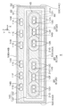
- FIG. 4 is a plan view of the semiconductor device shown in FIG.
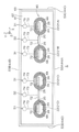
- FIG. 5 is a plan view showing a layer in which a low potential coil is formed in the semiconductor device of FIG.
- FIG. 6 is a plan view showing a layer in which a high potential coil is formed in the semiconductor device of FIG.
- FIG. 7 is a cross-sectional view taken along the line VIII-VIII shown in FIG.
- FIG. 8 is a diagram showing an enlarged view (separated structure) of the region XIII shown in FIG. 7.
- FIG. 8 is a diagram showing an enlarged view (separated structure) of the region XIII shown in FIG. 7.
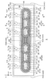
- FIG. 9 is a diagram schematically showing a layout example of the transformer chip.
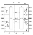
- FIG. 10 is a diagram showing an embodiment of a signal transmission device.
- FIG. 11 is a diagram showing a configuration example of an electronic device on which a signal transmission device is mounted.
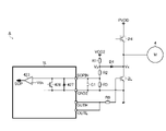
- FIG. 12 is a diagram showing a first connection example (DESAT method) of the short circuit detection terminal.
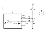
- FIG. 13 is a diagram showing a second connection example (emitter sense method) of the short circuit detection terminal.
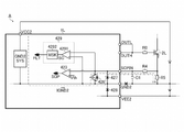
- FIG. 14 is a diagram showing a configuration example of an open detection circuit.
- FIG. 15 is a diagram showing an example of an open detection operation.
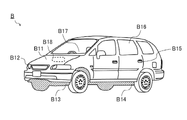
- FIG. 16 is a diagram showing the appearance of a vehicle on which an electronic device is mounted.
- FIG. 1 is a diagram showing a basic configuration of a signal transmission device.
- the signal transmission device 200 of this configuration example has the primary circuit system 200p to the secondary circuit system 200s while insulating between the primary circuit system 200p (VCC1-GND1 system) and the secondary circuit system 200s (VCC2-GND2 system).
- It is a semiconductor integrated circuit device (so-called isolated gate driver IC) that transmits a pulse signal to and drives a gate of a switch element (not shown) provided in the secondary circuit system 200s.
- the signal transmission device 200 includes a controller chip 210, a driver chip 220, and a transformer chip 230 sealed in a single package.
- the controller chip 210 is a semiconductor chip that operates by being supplied with a power supply voltage VCS1 (for example, a maximum of 7V based on GND1).
- VCS1 for example, a maximum of 7V based on GND1.
- the pulse transmission circuit 211 and the buffers 212 and 213 are integrated in the controller chip 210.
- the pulse transmission circuit 211 is a pulse generator that generates transmission pulse signals S11 and S21 according to the input pulse signal IN. More specifically, the pulse transmission circuit 211 performs pulse drive (single or multiple transmission pulse output) of the transmission pulse signal S11 when notifying that the input pulse signal IN is at a high level, and inputs the input pulse. When notifying that the signal IN is low level, the transmission pulse signal S21 is pulse-driven. That is, the pulse transmission circuit 211 pulse-drives either one of the transmission pulse signals S11 and S21 according to the logic level of the input pulse signal IN.
- the buffer 212 receives the input of the transmission pulse signal S11 from the pulse transmission circuit 211 and drives the transformer chip 230 (specifically, the transformer 231) in a pulse.
- the buffer 213 receives the input of the transmission pulse signal S21 from the pulse transmission circuit 211 and drives the transformer chip 230 (specifically, the transformer 232) in a pulse manner.
- the driver chip 220 is a semiconductor chip that operates by being supplied with a power supply voltage VCS2 (for example, a maximum of 30 V based on GND2).
- VCS2 for example, a maximum of 30 V based on GND2
- the buffers 221 and 222, the pulse receiving circuit 223, and the driver 224 are integrated in the driver chip 220.
- the buffer 221 waveform-shapes the received pulse signal S12 induced in the transformer chip 230 (specifically, the transformer 231) and outputs it to the pulse receiving circuit 223.
- the buffer 222 waveform-shapes the received pulse signal S22 induced in the transformer chip 230 (specifically, the transformer 232) and outputs it to the pulse receiving circuit 223.
- the pulse receiving circuit 223 generates an output pulse signal OUT by driving the driver 224 in response to the received pulse signals S12 and S22 input via the buffers 221 and 222. More specifically, the pulse receiving circuit 223 receives the pulse drive of the received pulse signal S12 to raise the output pulse signal OUT to a high level, while receives the pulse drive of the received pulse signal S22 to raise the output pulse signal OUT. Drive the driver 224 to lower to a low level. That is, the pulse receiving circuit 223 switches the logic level of the output pulse signal OUT according to the logic level of the input pulse signal IN. As the pulse receiving circuit 223, for example, an RS flip-flop can be preferably used.
- the driver 224 generates an output pulse signal OUT based on the drive control of the pulse receiving circuit 223.
- the transformer chip 230 receives the transmission pulse signals S11 and S21 input from the pulse transmission circuit 211, respectively, while insulating the controller chip 210 and the driver chip 220 in a direct current manner by using the transformers 231 and 232. And S22 are output to the pulse receiving circuit 223.
- DC insulating means that the object to be insulated is not connected by a conductor.
- the transformer 231 outputs the reception pulse signal S12 from the secondary coil 231s in response to the transmission pulse signal S11 input to the primary coil 231p.
- the transformer 232 outputs the received pulse signal S22 from the secondary coil 232s in response to the transmission pulse signal S21 input to the primary coil 232p.
- the signal transmission device 200 of this configuration example independently has a transformer chip 230 on which only the transformers 231 and 232 are mounted, in addition to the controller chip 210 and the driver chip 220, and these three chips are used as a single unit. It is sealed in a package.
- both the controller chip 210 and the driver chip 220 can be formed by a general low withstand voltage to medium withstand voltage process (withstand voltage of several V to several tens of V), and thus are dedicated. It is not necessary to use a high withstand voltage process (withstand voltage of several kV), and the manufacturing cost can be reduced.
- the signal transmission device 200 can be suitably used, for example, in a power supply device or a motor drive device of an in-vehicle device mounted on a vehicle.
- the above vehicles include electric vehicles (BEV [battery electric vehicle], HEV [hybrid electric vehicle], PHEV / PHV (plug-in hybrid electric vehicle / plug-in hybrid vehicle), or FCEV / FCV (xEV such as fuel cell electric vehicle / fuel cell vehicle) is also included.
- FIG. 2 is a diagram showing the basic structure of the transformer chip 230.
- the transformer 231 includes a primary coil 231p and a secondary coil 231s facing each other in the vertical direction.
- the transformer 232 includes a primary coil 232p and a secondary coil 232s facing each other in the vertical direction.
- Both the primary coil 231p and 232p are formed on the first wiring layer (lower layer) 230a of the transformer chip 230. Both the secondary coil 231s and 232s are formed on the second wiring layer (upper layer in this figure) 230b of the transformer chip 230.
- the secondary coil 231s is arranged directly above the primary coil 231p and faces the primary coil 231p. Further, the secondary coil 232s is arranged directly above the primary coil 232p and faces the primary coil 232p.
- the primary side coil 231p is laid spirally so as to surround the circumference of the internal terminal X21 in a clockwise direction starting from the first end connected to the internal terminal X21, and the second end corresponding to the end point thereof is inside. It is connected to the terminal X22.
- the primary side coil 232p is laid spirally so as to surround the circumference of the internal terminal X23 in a counterclockwise direction starting from the first end connected to the internal terminal X23, and the second end corresponding to the end point thereof. The end is connected to the internal terminal X22.
- the internal terminals X21, X22 and X23 are linearly arranged in the order shown in the figure.
- the internal terminal X21 is connected to the external terminal T21 of the second layer 230b via the conductive wiring Y21 and the via Z21.
- the internal terminal X22 is connected to the external terminal T22 of the second layer 230b via the conductive wiring Y22 and the via Z22.
- the internal terminal X23 is connected to the external terminal T23 of the second layer 230b via the conductive wiring Y23 and the via Z23.
- the external terminals T21 to T23 are arranged linearly side by side and are used for wire bonding with the controller chip 210.
- the secondary coil 231s is spirally laid so as to surround the circumference of the external terminal T24 in a counterclockwise direction starting from the first end connected to the external terminal T24, and the second end corresponding to the end point thereof. Is connected to the external terminal T25.
- the secondary side coil 232s is laid spirally so as to surround the circumference of the external terminal T26 in a clockwise direction starting from the first end connected to the external terminal T26, and the second end corresponding to the end point thereof. The end is connected to the external terminal T25.
- the external terminals T24, T25 and T26 are arranged linearly in the order shown in the drawing, and are used for wire bonding with the driver chip 220.
- the secondary coil 231s and 232s are AC-connected to the primary coils 231p and 232p by magnetic coupling, respectively, and are DC-insulated from the primary coils 231p and 232p, respectively. That is, the driver chip 220 is AC-connected to the controller chip 210 via the transformer chip 230, and is DC-insulated from the controller chip 210 by the transformer chip 230.
- FIG. 3 is a perspective view showing a semiconductor device 5 used as a 2-channel type transformer chip.
- FIG. 4 is a plan view of the semiconductor device 5 shown in FIG.
- FIG. 7 is a cross-sectional view taken along the line VIII-VIII shown in FIG.
- the semiconductor device 5 includes a rectangular parallelepiped semiconductor chip 41.
- the semiconductor chip 41 includes at least one of silicon, a wide bandgap semiconductor and a compound semiconductor.
- the wide bandgap semiconductor is composed of a semiconductor that exceeds the bandgap of silicon (about 1.12 eV). Wide bandgap The bandgap of the semiconductor is preferably 2.0 eV or more.
- the wide bandgap semiconductor may be SiC (silicon carbide).
- the compound semiconductor may be a group III-V compound semiconductor.
- the compound semiconductor may contain at least one of AlN (aluminum nitride), InN (indium nitride), GaN (gallium nitride) and GaAs (gallium arsenide).
- the semiconductor chip 41 includes a semiconductor substrate made of silicon.
- the semiconductor chip 41 may be an epitaxial substrate having a laminated structure including a silicon semiconductor substrate and a silicon epitaxial layer.
- the conductive type of the semiconductor substrate may be n-type or p-type.
- the epitaxial layer may be n-type or p-type.
- the semiconductor chip 41 has a first main surface 42 on one side, a second main surface 43 on the other side, and chip side walls 44A to 44D connecting the first main surface 42 and the second main surface 43.
- the first main surface 42 and the second main surface 43 are formed in a rectangular shape (rectangular shape in this form) in a plan view (hereinafter, simply referred to as “planar view”) viewed from their normal direction Z. ..
- the chip side walls 44A to 44D include a first chip side wall 44A, a second chip side wall 44B, a third chip side wall 44C, and a fourth chip side wall 44D.
- the first chip side wall 44A and the second chip side wall 44B form the long side of the semiconductor chip 41.
- the first chip side wall 44A and the second chip side wall 44B extend along the first direction X and face the second direction Y.
- the third chip side wall 44C and the fourth chip side wall 44D form the short side of the semiconductor chip 41.
- the third chip side wall 44C and the fourth chip side wall 44D extend in the second direction Y and face the first direction X.
- the chip side walls 44A to 44D are composed of a ground surface.
- the semiconductor device 5 further includes an insulating layer 51 formed on the first main surface 42 of the semiconductor chip 41.
- the insulating layer 51 has an insulating main surface 52 and insulating side walls 53A to 53D.
- the insulating main surface 52 is formed in a rectangular shape (rectangular shape in this form) that matches the first main surface 42 in a plan view.
- the insulating main surface 52 extends parallel to the first main surface 42.
- the insulating side walls 53A to 53D include a first insulating side wall 53A, a second insulating side wall 53B, a third insulating side wall 53C, and a fourth insulating side wall 53D.
- the insulating side walls 53A to 53D extend from the peripheral edge of the insulating main surface 52 toward the semiconductor chip 41 and are connected to the chip side walls 44A to 44D. Specifically, the insulating side walls 53A to 53D are formed flush with respect to the chip side walls 44A to 44D.
- the insulating side walls 53A to 53D form a flush grinding surface on the chip side walls 44A to 44D.
- the insulating layer 51 is composed of a multilayer insulating laminated structure including a lowermost insulating layer 55, an uppermost insulating layer 56, and a plurality of (11 layers in this form) interlayer insulating layers 57.
- the bottom insulating layer 55 is an insulating layer that directly covers the first main surface 42.
- the uppermost insulating layer 56 is an insulating layer forming the insulating main surface 52.
- the plurality of interlayer insulating layers 57 are insulating layers interposed between the lowermost insulating layer 55 and the uppermost insulating layer 56.
- the bottom insulating layer 55 in this form, has a single layer structure containing silicon oxide.
- the uppermost insulating layer 56 has a single-layer structure containing silicon oxide in this form.
- the thickness of the lowermost insulating layer 55 and the thickness of the uppermost insulating layer 56 may be 1 ⁇ m or more and 3 ⁇ m or less (for example, about 2 ⁇ m), respectively.
- the plurality of interlayer insulating layers 57 each have a laminated structure including a first insulating layer 58 on the lowermost insulating layer 55 side and a second insulating layer 59 on the uppermost insulating layer 56 side.
- the first insulating layer 58 may contain silicon nitride.
- the first insulating layer 58 is formed as an etching stopper layer for the second insulating layer 59.
- the thickness of the first insulating layer 58 may be 0.1 ⁇ m or more and 1 ⁇ m or less (for example, about 0.3 ⁇ m).
- the second insulating layer 59 is formed on the first insulating layer 58. It contains an insulating material different from that of the first insulating layer 58.
- the second insulating layer 59 may contain silicon oxide.
- the thickness of the second insulating layer 59 may be 1 ⁇ m or more and 3 ⁇ m or less (for example, about 2 ⁇ m). The thickness of the second insulating layer 59 preferably exceeds the thickness of the first insulating layer 58.
- the total thickness DT of the insulating layer 51 may be 5 ⁇ m or more and 50 ⁇ m or less.
- the total thickness DT of the insulating layer 51 and the number of layers of the interlayer insulating layer 57 are arbitrary and are adjusted according to the withstand voltage (dielectric breakdown resistance) to be realized.
- the insulating materials of the lowermost insulating layer 55, the uppermost insulating layer 56, and the interlayer insulating layer 57 are arbitrary and are not limited to a specific insulating material.
- the semiconductor device 5 includes a first functional device 45 formed on the insulating layer 51.
- the first functional device 45 includes one or more transformers 21 (corresponding to the transformers mentioned above). That is, the semiconductor device 5 is a multi-channel device including a plurality of transformers 21.
- the plurality of transformers 21 are formed in the inner portion of the insulating layer 51 at intervals from the insulating side walls 53A to 53D.
- the plurality of transformers 21 are formed at intervals in the first direction X.
- the plurality of transformers 21 are the first transformer 21A, the second transformer 21B, the third transformer 21C, and the first transformer 21A, the second transformer 21B, and the third transformer 21C formed in this order from the insulating side wall 53C side to the insulating side wall 53D side in a plan view.
- the plurality of transformers 21A to 21D each have a similar structure.
- the structure of the first transformer 21A will be described as an example.
- the description of the structure of the second transformer 21B, the third transformer 21C and the fourth transformer 21D the description of the structure of the first transformer 21A shall be applied mutatis mutandis and will be omitted.
- the first transformer 21A includes a low potential coil 22 and a high potential coil 23.
- the low potential coil 22 is formed in the insulating layer 51.
- the high-potential coil 23 is formed in the insulating layer 51 so as to face the low-potential coil 22 in the normal direction Z.
- the low-potential coil 22 and the high-potential coil 23 are formed in a region (that is, a plurality of interlayer insulating layers 57) sandwiched between the lowermost insulating layer 55 and the uppermost insulating layer 56.
- the low-potential coil 22 is formed in the insulating layer 51 on the lowermost insulating layer 55 (semiconductor chip 41) side, and the high-potential coil 23 has the uppermost insulating layer 56 in the insulating layer 51 with respect to the low-potential coil 22. It is formed on the (insulation main surface 52) side. That is, the high-potential coil 23 faces the semiconductor chip 41 with the low-potential coil 22 interposed therebetween.
- the location of the low-potential coil 22 and the high-potential coil 23 is arbitrary. Further, the high-potential coil 23 may face the low-potential coil 22 with one or more layers of the interlayer insulating layer 57 interposed therebetween.
- the distance between the low-potential coil 22 and the high-potential coil 23 (that is, the number of layers of the interlayer insulating layer 57) is appropriately adjusted according to the insulation withstand voltage and the electric field strength between the low-potential coil 22 and the high-potential coil 23.
- the low-potential coil 22 is formed in the interlayer insulating layer 57, which is the third layer counting from the lowermost insulating layer 55 side.
- the high potential coil 23 is formed on the interlayer insulating layer 57, which is the first layer counting from the uppermost insulating layer 56 side.
- the low-potential coil 22 is embedded in the interlayer insulating layer 57 so as to penetrate the first insulating layer 58 and the second insulating layer 59.
- the low potential coil 22 includes a first inner end 24, a first outer end 25, and a first spiral portion 26 spirally routed between the first inner end 24 and the first outer end 25.
- the first spiral portion 26 is drawn in a spiral shape extending in an elliptical shape (oval shape) in a plan view.
- the portion forming the innermost peripheral edge of the first spiral portion 26 defines the elliptical first inner region 66 in a plan view.
- the number of turns of the first spiral portion 26 may be 5 or more and 30 or less.
- the width of the first spiral portion 26 may be 0.1 ⁇ m or more and 5 ⁇ m or less.
- the width of the first spiral portion 26 is preferably 1 ⁇ m or more and 3 ⁇ m or less.
- the width of the first spiral portion 26 is defined by the width in the direction orthogonal to the spiral direction.
- the first winding pitch of the first spiral portion 26 may be 0.1 ⁇ m or more and 5 ⁇ m or less.
- the first winding pitch is preferably 1 ⁇ m or more and 3 ⁇ m or less.
- the first winding pitch is defined by the distance between two adjacent portions of the first spiral portion 26 in a direction orthogonal to the spiral direction.
- the winding shape of the first spiral portion 26 and the planar shape of the first inner region 66 are arbitrary and are not limited to the shapes shown in FIG. 5 and the like.
- the first spiral portion 26 may be wound into a polygonal shape such as a triangle shape or a quadrangular shape, or a circular shape in a plan view.
- the first inner region 66 may be divided into a polygonal shape such as a triangle shape, a quadrangular shape, or a circular shape in a plan view, depending on the winding shape of the first spiral portion 26.
- the low potential coil 22 may contain at least one of titanium, titanium nitride, copper, aluminum and tungsten.
- the low potential coil 22 may have a laminated structure including a barrier layer and a main body layer.
- the barrier layer partitions the recess space in the interlayer insulating layer 57.
- the barrier layer may contain at least one of titanium and titanium nitride.
- the body layer may contain at least one of copper, aluminum and tungsten.
- the high-potential coil 23 is embedded in the interlayer insulating layer 57 so as to penetrate the first insulating layer 58 and the second insulating layer 59.
- the high potential coil 23 includes a second inner end 27, a second outer end 28, and a second spiral portion 29 spirally routed between the second inner end 27 and the second outer end 28.
- the second spiral portion 29 is drawn in a spiral shape extending in an elliptical shape (oval shape) in a plan view.
- the portion forming the innermost peripheral edge of the second spiral portion 29, in this form partitions the second inner region 67 having an elliptical shape in a plan view.
- the second inner region 67 of the second spiral portion 29 faces the first inner region 66 of the first spiral portion 26 in the normal direction Z.
- the number of turns of the second spiral portion 29 may be 5 or more and 30 or less.
- the number of turns of the second spiral portion 29 with respect to the number of turns of the first spiral portion 26 is adjusted according to the voltage value to be boosted.
- the number of turns of the second spiral portion 29 preferably exceeds the number of turns of the first spiral portion 26.
- the number of turns of the second spiral portion 29 may be less than the number of turns of the first spiral portion 26, or may be equal to the number of turns of the first spiral portion 26.
- the width of the second spiral portion 29 may be 0.1 ⁇ m or more and 5 ⁇ m or less.
- the width of the second spiral portion 29 is preferably 1 ⁇ m or more and 3 ⁇ m or less.
- the width of the second spiral portion 29 is defined by the width in the direction orthogonal to the spiral direction.
- the width of the second spiral portion 29 is preferably equal to the width of the first spiral portion 26.
- the second winding pitch of the second spiral portion 29 may be 0.1 ⁇ m or more and 5 ⁇ m or less.
- the second winding pitch is preferably 1 ⁇ m or more and 3 ⁇ m or less.
- the second winding pitch is defined by the distance between two adjacent portions of the second spiral portion 29 in the direction orthogonal to the spiral direction.
- the second winding pitch is preferably equal to the first winding pitch of the first spiral portion 26.
- the winding shape of the second spiral portion 29 and the planar shape of the second inner region 67 are arbitrary and are not limited to the shapes shown in FIG. 6 and the like.
- the second spiral portion 29 may be wound into a polygonal shape such as a triangle shape or a quadrangular shape, or a circular shape in a plan view.
- the second inner region 67 may be divided into a polygonal shape such as a triangle shape, a quadrangular shape, or a circular shape in a plan view, depending on the winding shape of the second spiral portion 29.
- the high-potential coil 23 is preferably formed of the same conductive material as the low-potential coil 22. That is, the high-potential coil 23 preferably includes a barrier layer and a main body layer, similarly to the low-potential coil 22.
- the semiconductor device 5 includes a plurality of (12 in this figure) low-potential terminals 11 and a plurality of (12 in this figure) high-potential terminals 12.
- the plurality of low-potential terminals 11 are electrically connected to the low-potential coils 22 of the corresponding transformers 21A to 21D, respectively.
- the plurality of high-potential terminals 12 are electrically connected to the high-potential coils 23 of the corresponding transformers 21A to 21D, respectively.
- the plurality of low potential terminals 11 are formed on the insulating main surface 52 of the insulating layer 51. Specifically, the plurality of low potential terminals 11 are formed in the region on the insulating side wall 53B side at intervals in the second direction Y from the plurality of transformers 21A to 21D, and are arranged at intervals in the first direction X. Has been done.
- the plurality of low-potential terminals 11 include a first low-potential terminal 11A, a second low-potential terminal 11B, a third low-potential terminal 11C, a fourth low-potential terminal 11D, a fifth low-potential terminal 11E, and a sixth low-potential terminal 11F. include. In this embodiment, two low-potential terminals 11A to 11F are formed, respectively. The number of the plurality of low potential terminals 11A to 11F is arbitrary.
- the first low potential terminal 11A faces the first transformer 21A in the second direction Y in a plan view.
- the second low potential terminal 11B faces the second transformer 21B in the second direction Y in a plan view.
- the third low potential terminal 11C faces the third transformer 21C in the second direction Y in a plan view.
- the fourth low potential terminal 11D faces the fourth transformer 21D in the second direction Y in a plan view.
- the fifth low-potential terminal 11E is formed in a region between the first low-potential terminal 11A and the second low-potential terminal 11B in a plan view.
- the sixth low-potential terminal 11F is formed in a region between the third low-potential terminal 11C and the fourth low-potential terminal 11D in a plan view.
- the first low potential terminal 11A is electrically connected to the first inner terminal 24 of the first transformer 21A (low potential coil 22).
- the second low-potential terminal 11B is electrically connected to the first inner end 24 of the second transformer 21B (low-potential coil 22).
- the third low-potential terminal 11C is electrically connected to the first inner end 24 of the third transformer 21C (low-potential coil 22).
- the fourth low-potential terminal 11D is electrically connected to the first inner end 24 of the fourth transformer 21D (low-potential coil 22).
- the fifth low potential terminal 11E is electrically connected to the first outer end 25 of the first transformer 21A (low potential coil 22) and the first outer end 25 of the second transformer 21B (low potential coil 22). There is.
- the sixth low potential terminal 11F is electrically connected to the first outer end 25 of the third transformer 21C (low potential coil 22) and the first outer end 25 of the fourth transformer 21D (low potential coil 22). There is.
- the plurality of high-potential terminals 12 are formed on the insulating main surface 52 of the insulating layer 51 at intervals from the plurality of low-potential terminals 11. Specifically, the plurality of high-potential terminals 12 are formed in the region on the insulating side wall 53A side at intervals in the second direction Y from the plurality of low-potential terminals 11, and are arranged at intervals in the first direction X. ing.
- the plurality of high-potential terminals 12 are each formed in a region close to the corresponding transformers 21A to 21D in a plan view.
- the fact that the high-potential terminal 12 is close to the transformers 21A to 21D means that the distance between the high-potential terminal 12 and the transformer 21 is less than the distance between the low-potential terminal 11 and the high-potential terminal 12 in a plan view. means.
- the plurality of high potential terminals 12 are formed at intervals along the first direction X so as to face the plurality of transformers 21A to 21D along the first direction X in a plan view. .. More specifically, the plurality of high-potential terminals 12 are located along the first direction X so as to be located in a region between the second inner region 67 of the high-potential coil 23 and the adjacent high-potential coils 23 in a plan view. It is formed at intervals. As a result, the plurality of high-potential terminals 12 are arranged side by side with the plurality of transformers 21A to 21D in the first direction X in a plan view.
- the plurality of high-potential terminals 12 include a first high-potential terminal 12A, a second high-potential terminal 12B, a third high-potential terminal 12C, a fourth high-potential terminal 12D, a fifth high-potential terminal 12E, and a sixth high-potential terminal 12F. include. In this embodiment, two high-potential terminals 12A to 12F are formed, respectively. The number of the plurality of high potential terminals 12A to 12F is arbitrary.
- the first high-potential terminal 12A is formed in the second inner region 67 of the first transformer 21A (high-potential coil 23) in a plan view.
- the second high-potential terminal 12B is formed in the second inner region 67 of the second transformer 21B (high-potential coil 23) in a plan view.
- the third high-potential terminal 12C is formed in the second inner region 67 of the third transformer 21C (high-potential coil 23) in a plan view.
- the fourth high-potential terminal 12D is formed in the second inner region 67 of the fourth transformer 21D (high-potential coil 23) in a plan view.
- the fifth high potential terminal 12E is formed in the region between the first transformer 21A and the second transformer 21B in a plan view.
- the sixth high potential terminal 12F is formed in a region between the third transformer 21C and the fourth transformer 21D in a plan view.
- the first high potential terminal 12A is electrically connected to the second inner end 27 of the first transformer 21A (high potential coil 23).
- the second high-potential terminal 12B is electrically connected to the second inner end 27 of the second transformer 21B (high-potential coil 23).
- the third high-potential terminal 12C is electrically connected to the second inner end 27 of the third transformer 21C (high-potential coil 23).
- the fourth high potential terminal 12D is electrically connected to the second inner end 27 of the fourth transformer 21D (high potential coil 23).
- the fifth high potential terminal 12E is electrically connected to the second outer end 28 of the first transformer 21A (high potential coil 23) and the second outer end 28 of the second transformer 21B (high potential coil 23). There is.
- the sixth high potential terminal 12F is electrically connected to the second outer end 28 of the third transformer 21C (high potential coil 23) and the second outer end 28 of the fourth transformer 21D (high potential coil 23). There is.
- the semiconductor device 5 includes a first low-potential wiring 31, a second low-potential wiring 32, a first high-potential wiring 33, and a second high-potential wiring formed in the insulating layer 51, respectively. Including 34.
- a plurality of first low-potential wirings 31, a plurality of second low-potential wirings 32, a plurality of first high-potential wirings 33, and a plurality of second high-potential wirings 34 are formed.
- the first low-potential wiring 31 and the second low-potential wiring 32 fix the low-potential coil 22 of the first transformer 21A and the low-potential coil 22 of the second transformer 21B to the same potential. Further, in the first low-potential wiring 31 and the second low-potential wiring 32, the low-potential coil 22 of the third transformer 21C and the low-potential coil 22 of the fourth transformer 21D are fixed at the same potential. In this embodiment, the first low-potential wiring 31 and the second low-potential wiring 32 fix all the low-potential coils 22 of the transformers 21A to 21D to the same potential.
- the first high-potential wiring 33 and the second high-potential wiring 34 fix the high-potential coil 23 of the first transformer 21A and the high-potential coil 23 of the second transformer 21B to the same potential. Further, the first high-potential wiring 33 and the second high-potential wiring 34 fix the high-potential coil 23 of the third transformer 21C and the high-potential coil 23 of the fourth transformer 21D to the same potential. In this embodiment, the first high-potential wiring 33 and the second high-potential wiring 34 fix all the high-potential coils 23 of the transformers 21A to 21D to the same potential.
- the plurality of first low-potential wirings 31 are electrically connected to the first inner end 24 of the corresponding low-potential terminals 11A to 11D and the corresponding transformers 21A to 21D (low-potential coil 22), respectively.
- the plurality of first low-potential wirings 31 have a similar structure.
- the structure of the first low-potential wiring 31 connected to the first low-potential terminal 11A and the first transformer 21A will be described as an example.
- the description of the structure of the other first low-potential wiring 31 shall be applied mutatis mutandis and will be omitted.
- the first low-potential wiring 31 includes a through wiring 71, a low-potential connection wiring 72, a lead-out wiring 73, a first connection plug electrode 74, a second connection plug electrode 75, and one or more (plural) pad plug electrodes. 76 and one or more (s) substrate plug electrodes 77 in this form.
- the through wiring 71, the low potential connection wiring 72, the lead wiring 73, the first connection plug electrode 74, the second connection plug electrode 75, the pad plug electrode 76, and the substrate plug electrode 77 are made of the same conductive material as the low potential coil 22 and the like. It is preferable that each is formed. That is, the through wiring 71, the low potential connection wiring 72, the lead wiring 73, the first connection plug electrode 74, the second connection plug electrode 75, the pad plug electrode 76, and the substrate plug electrode 77 are the same as the low potential coil 22 and the like. It is preferable to include a barrier layer and a main body layer, respectively.
- the penetrating wiring 71 penetrates a plurality of interlayer insulating layers 57 in the insulating layer 51 and extends in a columnar shape extending along the normal direction Z.
- the through wiring 71 is formed in the region between the lowermost insulating layer 55 and the uppermost insulating layer 56 in the insulating layer 51.
- the through wiring 71 has an upper end portion on the uppermost insulating layer 56 side and a lower end portion on the lowermost insulating layer 55 side.
- the upper end of the through wiring 71 is formed in the same interlayer insulating layer 57 as the high potential coil 23, and is covered with the uppermost insulating layer 56.
- the lower end of the through wiring 71 is formed in the same interlayer insulating layer 57 as the low potential coil 22.
- the through wiring 71 includes a first electrode layer 78, a second electrode layer 79, and a plurality of wiring plug electrodes 80.
- the first electrode layer 78, the second electrode layer 79, and the wiring plug electrode 80 are each formed of the same conductive material as the low potential coil 22 and the like. That is, the first electrode layer 78, the second electrode layer 79, and the wiring plug electrode 80 include a barrier layer and a main body layer, respectively, like the low potential coil 22 and the like.
- the first electrode layer 78 forms the upper end portion of the through wiring 71.
- the second electrode layer 79 forms the lower end portion of the through wiring 71.
- the first electrode layer 78 is formed in an island shape and faces the low potential terminal 11 (first low potential terminal 11A) in the normal direction Z.
- the second electrode layer 79 is formed in an island shape and faces the first electrode layer 78 in the normal direction Z.
- the plurality of wiring plug electrodes 80 are embedded in the plurality of interlayer insulating layers 57 located in the region between the first electrode layer 78 and the second electrode layer 79, respectively.
- the plurality of wiring plug electrodes 80 are laminated from the lowest insulating layer 55 toward the uppermost insulating layer 56 so as to be electrically connected to each other, and the first electrode layer 78 and the second electrode layer 79 are electrically connected. You are connected.
- the plurality of wiring plug electrodes 80 each have a flat area of the first electrode layer 78 and a flat area less than the flat area of the second electrode layer 79.
- the number of layers of the plurality of wiring plug electrodes 80 matches the number of layers of the plurality of interlayer insulating layers 57.
- six wiring plug electrodes 80 are embedded in each interlayer insulating layer 57, but the number of wiring plug electrodes 80 embedded in each interlayer insulating layer 57 is arbitrary.
- one or a plurality of wiring plug electrodes 80 may be formed so as to penetrate the plurality of interlayer insulating layers 57.
- the low-potential connection wiring 72 is formed in the first inner region 66 of the first transformer 21A (low-potential coil 22) in the same interlayer insulating layer 57 as the low-potential coil 22.
- the low-potential connection wiring 72 is formed in an island shape and faces the high-potential terminal 12 (first high-potential terminal 12A) in the normal direction Z.
- the low-potential connection wiring 72 preferably has a flat area that exceeds the flat area of the wiring plug electrode 80.
- the low-potential connection wiring 72 is electrically connected to the first inner end 24 of the low-potential coil 22.
- the lead-out wiring 73 is formed in the region between the semiconductor chip 41 and the through wiring 71 in the interlayer insulating layer 57.
- the lead-out wiring 73 is formed in the interlayer insulating layer 57, which is the first layer counting from the lowest insulating layer 55.
- the lead-out wiring 73 includes a first end portion on one side, a second end portion on the other side, and a wiring portion connecting the first end portion and the second end portion.
- the first end of the lead-out wiring 73 is located in the region between the semiconductor chip 41 and the lower end of the through wiring 71.
- the second end of the lead wire 73 is located in the region between the semiconductor chip 41 and the low potential connection wire 72.
- the wiring portion extends along the first main surface 42 of the semiconductor chip 41, and extends in a band shape in the region between the first end portion and the second end portion.
- the first connection plug electrode 74 is formed in the region between the through wiring 71 and the lead wiring 73 in the interlayer insulating layer 57, and is electrically connected to the first end portion of the through wiring 71 and the lead wiring 73.
- the second connection plug electrode 75 is formed in the region between the low-potential connection wiring 72 and the lead-out wiring 73 in the interlayer insulating layer 57, and is electrically connected to the second end portion of the low-potential connection wiring 72 and the lead-out wiring 73. Has been done.
- the plurality of pad plug electrodes 76 are formed in the region between the low potential terminal 11 (first low potential terminal 11A) and the through wiring 71 in the uppermost insulating layer 56, and are formed at the upper ends of the low potential terminal 11 and the through wiring 71. Each is electrically connected.
- the plurality of substrate plug electrodes 77 are formed in the region between the semiconductor chip 41 and the lead-out wiring 73 in the lowermost insulating layer 55. In this embodiment, the substrate plug electrode 77 is formed in a region between the semiconductor chip 41 and the first end portion of the lead wire 73, and is electrically connected to the first end portion of the semiconductor chip 41 and the lead wire 73, respectively. There is.
- the plurality of first high-potential wirings 33 are located at the second inner ends 27 of the corresponding high-potential terminals 12A to 12D and the corresponding transformers 21A to 21D (high-potential coil 23), respectively. It is electrically connected.
- the plurality of first high-potential wirings 33 each have a similar structure.
- the structure of the first high-potential wiring 33 connected to the first high-potential terminal 12A and the first transformer 21A will be described as an example.
- the description of the structure of the other first high-potential wiring 33 the description of the structure of the first high-potential wiring 33 connected to the first transformer 21A shall be applied mutatis mutandis and will be omitted.
- the first high-potential wiring 33 includes a high-potential connection wiring 81 and one or more (plural in this form) pad plug electrodes 82.
- the high-potential connection wiring 81 and the pad plug electrode 82 are preferably formed of the same conductive material as the low-potential coil 22 and the like. That is, it is preferable that the high-potential connection wiring 81 and the pad plug electrode 82 include a barrier layer and a main body layer, similarly to the low-potential coil 22 and the like.
- the high-potential connection wiring 81 is formed in the second inner region 67 of the high-potential coil 23 in the same interlayer insulating layer 57 as the high-potential coil 23.
- the high-potential connection wiring 81 is formed in an island shape and faces the high-potential terminal 12 (first high-potential terminal 12A) in the normal direction Z.
- the high-potential connection wiring 81 is electrically connected to the second inner end 27 of the high-potential coil 23.
- the high-potential connection wiring 81 is formed at a distance from the low-potential connection wiring 72 in a plan view, and does not face the low-potential connection wiring 72 in the normal direction Z. As a result, the insulating distance between the low-potential connection wiring 72 and the high-potential connection wiring 81 is increased, and the withstand voltage of the insulating layer 51 is increased.
- the plurality of pad plug electrodes 82 are formed in the region between the high potential terminal 12 (first high potential terminal 12A) and the high potential connection wiring 81 in the uppermost insulating layer 56, and the high potential terminal 12 and the high potential connection wiring 81 are formed. Are electrically connected to each.
- the plurality of pad plug electrodes 82 each have a flat area smaller than the flat area of the high potential connection wiring 81 in a plan view.
- the distance D1 between the low-potential terminal 11 and the high-potential terminal 12 preferably exceeds the distance D2 between the low-potential coil 22 and the high-potential coil 23 (D2 ⁇ D1).
- the distance D1 preferably exceeds the total thickness DT of the plurality of interlayer insulating layers 57 (DT ⁇ D1).
- the ratio D2 / D1 of the distance D2 to the distance D1 may be 0.01 or more and 0.1 or less.
- the distance D1 is preferably 100 ⁇ m or more and 500 ⁇ m or less.
- the distance D2 may be 1 ⁇ m or more and 50 ⁇ m or less.
- the distance D2 is preferably 5 ⁇ m or more and 25 ⁇ m or less.
- the values of the distance D1 and the distance D2 are arbitrary and are appropriately adjusted according to the withstand voltage to be realized.
- the semiconductor device 5 includes a dummy pattern 85 embedded in the insulating layer 51 so as to be located around the transformers 21A to 21D in a plan view.
- the dummy pattern 85 is formed of a pattern (discontinuous pattern) different from that of the high-potential coil 23 and the low-potential coil 22, and is independent of the transformers 21A to 21D. That is, the dummy pattern 85 does not function as the transformers 21A to 21D.
- the dummy pattern 85 is formed as a shield conductor layer that shields the electric field between the low potential coil 22 and the high potential coil 23 in the transformers 21A to 21D and suppresses the electric field concentration on the high potential coil 23.
- the dummy pattern 85 is routed at a line density equal to the line density of the high potential coil 23 per unit area.
- the fact that the line density of the dummy pattern 85 is equal to the line density of the high potential coil 23 means that the line density of the dummy pattern 85 is within ⁇ 20% of the line density of the high potential coil 23.
- the depth position of the dummy pattern 85 inside the insulating layer 51 is arbitrary and is adjusted according to the electric field strength to be relaxed.
- the dummy pattern 85 is preferably formed in a region close to the high potential coil 23 with respect to the low potential coil 22 in the normal direction Z.
- the fact that the dummy pattern 85 is close to the high-potential coil 23 in the normal direction Z means that the distance between the dummy pattern 85 and the high-potential coil 23 is between the dummy pattern 85 and the low-potential coil 22 in the normal direction Z. Means less than the distance.
- the electric field concentration on the high potential coil 23 can be appropriately suppressed.
- the dummy pattern 85 is preferably formed in the same interlayer insulating layer 57 as the high potential coil 23. In this case, the electric field concentration on the high potential coil 23 can be suppressed more appropriately.
- the dummy pattern 85 includes a plurality of dummy patterns having different electrical states.
- the dummy pattern 85 may include a high potential dummy pattern.
- the depth position of the high potential dummy pattern 86 inside the insulating layer 51 is arbitrary, and is adjusted according to the electric field strength to be relaxed.
- the high-potential dummy pattern 86 is preferably formed in a region close to the high-potential coil 23 with respect to the low-potential coil 22 in the normal direction Z.
- the fact that the high-potential dummy pattern 86 is close to the high-potential coil 23 in the normal direction Z means that the distance between the high-potential dummy pattern 86 and the high-potential coil 23 in the normal direction Z is the high-potential dummy pattern 86 and the low-potential. It means that it is less than the distance between the coils 22.
- the dummy pattern 85 includes a floating dummy pattern formed in an electrically floating state in the insulating layer 51 so as to be located around the transformers 21A to 21D.
- the floating dummy pattern is drawn in a dense line shape so as to partially cover the area around the high potential coil 23 and partially expose it in a plan view.
- the floating dummy pattern may be formed in an endless shape or may be formed in an endless shape.
- the depth position of the floating dummy pattern inside the insulating layer 51 is arbitrary and is adjusted according to the electric field strength to be relaxed.
- the number of floating lines is arbitrary and is adjusted according to the electric field to be relaxed.
- the floating dummy pattern may be composed of a plurality of floating.
- the semiconductor device 5 includes a second functional device 60 formed on the first main surface 42 of the semiconductor chip 41 in the device region 62.
- the second functional device 60 is formed by utilizing the surface layer portion of the first main surface 42 of the semiconductor chip 41 and / or the region above the first main surface 42 of the semiconductor chip 41, and is formed by utilizing the insulating layer 51 (bottom). It is covered with an insulating layer 55).
- the second functional device 60 is shown simplified by the broken line shown on the surface layer of the first main surface 42.
- the second function device 60 is electrically connected to the low potential terminal 11 via the low potential wiring and electrically connected to the high potential terminal 12 via the high potential wiring.
- the low-potential wiring has the same structure as the first low-potential wiring 31 (second low-potential wiring 32) except that the low-potential wiring is routed in the insulating layer 51 so as to be connected to the second functional device 60.
- the high-potential wiring has the same structure as the first high-potential wiring 33 (second high-potential wiring 34) except that the high-potential wiring is routed in the insulating layer 51 so as to be connected to the second functional device 60.
- Specific description of the low-potential wiring and the high-potential wiring according to the second function device 60 will be omitted.
- the second function device 60 may include at least one of a passive device, a semiconductor rectifying device and a semiconductor switching device.
- the passive device the second functional device 60 may include a network in which any two or more kinds of devices among passive devices, semiconductor rectifying devices and semiconductor switching devices are selectively combined.
- the network may form part or all of the integrated circuit.
- the passive device may include a semiconductor passive device. Passive devices may include resistances and / or capacitors.
- the semiconductor rectifying device may include at least one of a pn junction diode, a PIN diode, a Zener diode, a Schottky barrier diode and a fast recovery diode.
- the semiconductor switching device may include at least one of BJT [Bipolar Junction Transistor], MISFET [Metal Insulator Field Effect Transistor], IGBT [Insulated Gate Bipolar Junction Transistor], and JFET [Junction Field Effect Transistor].
- the semiconductor device 5 further includes a seal conductor 61 embedded in the insulating layer 51.
- the seal conductor 61 is embedded in the insulating layer 51 in a wall shape at intervals from the insulating side walls 53A to 53D in a plan view, and the insulating layer 51 is divided into a device region 62 and an outer region 63.
- the seal conductor 61 suppresses the ingress of moisture and the ingress of cracks from the outer region 63 into the device region 62.
- the device area 62 includes a first functional device 45 (a plurality of transformers 21), a second functional device 60, a plurality of low potential terminals 11, a plurality of high potential terminals 12, a first low potential wiring 31, and a second low potential wiring. 32, a region including a first high-potential wiring 33, a second high-potential wiring 34, and a dummy pattern 85.
- the outer region 63 is an region outside the device region 62.
- the seal conductor 61 is electrically separated from the device area 62.
- the seal conductor 61 includes a first functional device 45 (a plurality of transformers 21), a second functional device 60, a plurality of low potential terminals 11, a plurality of high potential terminals 12, and a first low potential wiring 31. It is electrically separated from the second low-potential wiring 32, the first high-potential wiring 33, the second high-potential wiring 34, and the dummy pattern 85. More specifically, the seal conductor 61 is electrically fixed in a floating state. The seal conductor 61 does not form a current path leading to the device region 62.
- the seal conductor 61 is formed in a strip shape along the insulating side walls 53 to 53D in a plan view.
- the seal conductor 61 is formed in a square ring (specifically, a rectangular ring) in a plan view.
- the seal conductor 61 partitions the device region 62 having a rectangular shape (specifically, a rectangular shape) in a plan view.
- the seal conductor 61 partitions the outer region 63 of the square ring (specifically, the rectangular ring) surrounding the device region 62 in a plan view.
- the seal conductor 61 has an upper end portion on the insulating main surface 52 side, a lower end portion on the semiconductor chip 41 side, and a wall portion extending like a wall between the upper end portion and the lower end portion.
- the upper end portion of the seal conductor 61 is formed at a distance from the insulating main surface 52 to the semiconductor chip 41 side, and is located in the insulating layer 51.
- the upper end of the seal conductor 61 is covered with the uppermost insulating layer 56 in this form.
- the upper end of the seal conductor 61 may be covered with one or more interlayer insulating layers 57.
- the upper end portion of the seal conductor 61 may be exposed from the uppermost insulating layer 56.
- the lower end portion of the seal conductor 61 is formed at a distance from the semiconductor chip 41 toward the upper end portion side.
- the seal conductor 61 is embedded in the insulating layer 51 so as to be located on the semiconductor chip 41 side with respect to the plurality of low-potential terminals 11 and the plurality of high-potential terminals 12. Further, in the insulating layer 51, the seal conductor 61 includes a first functional device 45 (a plurality of transformers 21), a first low potential wiring 31, a second low potential wiring 32, a first high potential wiring 33, and a second high potential. It faces the wiring 34 and the dummy pattern 85 in a direction parallel to the insulating main surface 52. The seal conductor 61 may face a part of the second functional device 60 in the insulating layer 51 in a direction parallel to the insulating main surface 52.
- the seal conductor 61 includes a plurality of seal plug conductors 64 and one or more (plural in this form) seal via conductor 65.
- the number of seal via conductors 65 is arbitrary.
- the uppermost seal plug conductor 64 among the plurality of seal plug conductors 64 forms the upper end portion of the seal conductor 61.
- Each of the plurality of seal via conductors 65 forms a lower end portion of the seal conductor 61.
- the seal plug conductor 64 and the seal via conductor 65 are preferably formed of the same conductive material as the low potential coil 22. That is, it is preferable that the seal plug conductor 64 and the seal via conductor 65 include a barrier layer and a main body layer as in the case of the low potential coil 22 and the like.
- the plurality of seal plug conductors 64 are each embedded in the plurality of interlayer insulating layers 57, and are formed in a square ring (specifically, a rectangular ring) surrounding the device region 62 in a plan view.
- the plurality of seal plug conductors 64 are laminated from the lowermost insulating layer 55 toward the uppermost insulating layer 56 so as to be connected to each other.
- the number of layers of the plurality of seal plug conductors 64 corresponds to the number of layers of the plurality of interlayer insulating layers 57.
- one or more seal plug conductors 64 may be formed so as to penetrate the plurality of interlayer insulating layers 57.
- one annular seal conductor 61 is formed by an aggregate of a plurality of seal plug conductors 64, it is not necessary that all of the plurality of seal plug conductors 64 are formed in an annular shape.
- at least one of the plurality of seal plug conductors 64 may be formed in an endped shape.
- at least one of the plurality of seal plug conductors 64 may be divided into a plurality of endped strip-shaped portions.
- the plurality of seal plug conductors 64 are formed in an endless shape (annular shape).
- the plurality of seal via conductors 65 are each formed in the region between the semiconductor chip 41 and the seal plug conductor 64 in the lowermost insulating layer 55.
- the plurality of seal via conductors 65 are formed at intervals from the semiconductor chip 41 and are connected to the seal plug conductor 64.
- the plurality of seal via conductors 65 have a flat area smaller than the flat area of the seal plug conductor 64.
- the single seal via conductor 65 may have a flat area equal to or larger than the flat area of the seal plug conductor 64.
- the width of the seal conductor 61 may be 0.1 ⁇ m or more and 10 ⁇ m or less.
- the width of the seal conductor 61 is preferably 1 ⁇ m or more and 5 ⁇ m or less.
- the width of the seal conductor 61 is defined by the width in the direction orthogonal to the direction in which the seal conductor 61 extends.
- the semiconductor device 5 further includes a separation structure 130 that is interposed between the semiconductor chip 41 and the seal conductor 61 and electrically separates the seal conductor 61 from the semiconductor chip 41.
- the separation structure 130 preferably contains an insulator.
- the separation structure 130 is composed of a field insulating film 131 formed on the first main surface 42 of the semiconductor chip 41.
- the field insulating film 131 includes at least one of an oxide film (silicon oxide film) and a nitride film (silicon nitride film).
- the field insulating film 131 is preferably made of a LOCOS (local oxidation of silicon) film as an example of an oxide film formed by oxidation of the first main surface 42 of the semiconductor chip 41.
- the thickness of the field insulating film 131 is arbitrary as long as it can insulate the semiconductor chip 41 and the seal conductor 61.
- the thickness of the field insulating film 131 may be 0.1 ⁇ m or more and 5 ⁇ m or less.
- the separation structure 130 is formed on the first main surface 42 of the semiconductor chip 41 and extends in a strip shape along the seal conductor 61 in a plan view.
- the separated structure 130 is formed in a square ring (specifically, a rectangular ring) in a plan view.
- the separation structure 130 has a connection portion 132 to which the lower end portion (seal via conductor 65) of the seal conductor 61 is connected.
- the connecting portion 132 may form an anchor portion in which the lower end portion (seal via conductor 65) of the seal conductor 61 bites toward the semiconductor chip 41 side.
- the connecting portion 132 may be formed flush with respect to the main surface of the separation structure 130.
- the separation structure 130 includes an inner end portion 130A on the device region 62 side, an outer end portion 130B on the outer region 63 side, and a main body portion 130C between the inner end portion 130A and the outer end portion 130B.
- the inner end portion 130A partitions a region (that is, a device region 62) in which the second functional device 60 is formed in a plan view.
- the inner end portion 130A may be integrally formed with an insulating film (not shown) formed on the first main surface 42 of the semiconductor chip 41.
- the outer end portion 130B is exposed from the chip side walls 44A to 44D of the semiconductor chip 41 and is connected to the chip side walls 44A to 44D of the semiconductor chip 41. More specifically, the outer end portion 130B is formed flush with respect to the chip side walls 44A to 44D of the semiconductor chip 41. The outer end portion 130B forms a flush ground surface between the chip side walls 44A to 44D of the semiconductor chip 41 and the insulating side walls 53A to 53D of the insulating layer 51. Of course, in other forms, the outer end portion 130B may be formed in the first main surface 42 at a distance from the chip side walls 44A to 44D.
- the main body 130C has a flat surface extending substantially parallel to the first main surface 42 of the semiconductor chip 41.
- the main body portion 130C has a connecting portion 132 to which the lower end portion (seal via conductor 65) of the seal conductor 61 is connected.
- the connecting portion 132 is formed in a portion of the main body portion 130C at a distance from the inner end portion 130A and the outer end portion 130B.
- the separation structure 130 may take various forms other than the field insulating film 131.
- the semiconductor device 5 further includes an inorganic insulating layer 140 formed on the insulating main surface 52 of the insulating layer 51 so as to cover the seal conductor 61.
- the inorganic insulating layer 140 may be referred to as a passivation layer.
- the inorganic insulating layer 140 protects the insulating layer 51 and the semiconductor chip 41 from above the insulating main surface 52.
- the inorganic insulating layer 140 has a laminated structure including the first inorganic insulating layer 141 and the second inorganic insulating layer 142.
- the first inorganic insulating layer 141 may contain silicon oxide.
- the first inorganic insulating layer 141 preferably contains USG (undoped silicate glass), which is silicon oxide without impurities.
- the thickness of the first inorganic insulating layer 141 may be 50 nm or more and 5000 nm or less.
- the second inorganic insulating layer 142 may contain silicon nitride.
- the thickness of the second inorganic insulating layer 142 may be 500 nm or more and 5000 nm or less.
- the breakdown voltage (V / cm) of USG exceeds the breakdown voltage (V / cm) of silicon nitride. Therefore, when the inorganic insulating layer 140 is thickened, it is preferable that the first inorganic insulating layer 141, which is thicker than the second inorganic insulating layer 142, is formed.
- the first inorganic insulating layer 141 may contain at least one of BPSG (boron doped phosphor silicate glass) and PSG (phosphorus silicate glass) as an example of silicon oxide. However, in this case, since impurities (boron or phosphorus) are contained in the silicon oxide, it is particularly preferable to form the first inorganic insulating layer 141 made of USG in order to increase the withstand voltage on the high potential coil 23. ..
- the inorganic insulating layer 140 may have a single-layer structure composed of either the first inorganic insulating layer 141 or the second inorganic insulating layer 142.
- the inorganic insulating layer 140 covers the entire area of the seal conductor 61 and has a plurality of low-potential pad openings 143 and a plurality of high-potential pad openings 144 formed in a region outside the seal conductor 61.
- the plurality of low-potential pad openings 143 each expose the plurality of low-potential terminals 11.
- the plurality of high-potential pad openings 144 expose the plurality of high-potential terminals 12, respectively.
- the inorganic insulating layer 140 may have an overlapping portion that rides on the peripheral edge portion of the low potential terminal 11.
- the inorganic insulating layer 140 may have an overlapping portion that rides on the peripheral edge portion of the high potential terminal 12.
- the semiconductor device 5 further includes an organic insulating layer 145 formed on the inorganic insulating layer 140.
- the organic insulating layer 145 may contain a photosensitive resin.
- the organic insulating layer 145 may contain at least one of polyimide, polyamide and polybenzoxazole.
- the organic insulating layer 145 contains polyimide in this form.
- the thickness of the organic insulating layer 145 may be 1 ⁇ m or more and 50 ⁇ m or less.
- the thickness of the organic insulating layer 145 preferably exceeds the total thickness of the inorganic insulating layer 140. Further, the total thickness of the inorganic insulating layer 140 and the organic insulating layer 145 is preferably a distance D2 or more between the low potential coil 22 and the high potential coil 23. In this case, the total thickness of the inorganic insulating layer 140 is preferably 2 ⁇ m or more and 10 ⁇ m or less. Further, the thickness of the organic insulating layer 145 is preferably 5 ⁇ m or more and 50 ⁇ m or less.
- the thickness of the inorganic insulating layer 140 and the organic insulating layer 145 can be suppressed, and at the same time, the withstand voltage on the high potential coil 23 is appropriately increased by the laminated film of the inorganic insulating layer 140 and the organic insulating layer 145. be able to.
- the organic insulating layer 145 includes a first portion 146 that covers the region on the low potential side and a second portion 147 that covers the region on the high potential side.
- the first portion 146 covers the seal conductor 61 with the inorganic insulating layer 140 interposed therebetween.
- the first portion 146 has a plurality of low-potential terminal openings 148 that each expose a plurality of low-potential terminals 11 (low-potential pad openings 143) in a region outside the seal conductor 61.
- the first portion 146 may have an overlap portion that rides on the peripheral edge (overlap portion) of the low potential pad opening 143.
- the second portion 147 is formed at a distance from the first portion 146, and the inorganic insulating layer 140 is exposed from between the second portion 147 and the first portion 146.
- the second portion 147 has a plurality of high-potential terminal openings 149 each exposing the plurality of high-potential terminals 12 (high-potential pad openings 144).
- the second portion 147 may have an overlap portion that rides on the peripheral edge (overlap portion) of the high potential pad opening 144.
- the second part 147 collectively covers the transformers 21A to 21D and the dummy pattern 85. Specifically, the second portion 147 collectively covers a plurality of high-potential coils 23, a plurality of high-potential terminals 12, a first high-potential dummy pattern 87, a second high-potential dummy pattern 88, and a floating dummy pattern 121. is doing.
- the embodiment of the present invention can be implemented in still another embodiment.
- an example in which the first functional device 45 and the second functional device 60 are formed has been described.
- a form having only the second functional device 60 without having the first functional device 45 may be adopted.
- the dummy pattern 85 may be removed.
- the second functional device 60 can have the same effect as the effect described in the first embodiment (excluding the effect related to the dummy pattern 85).
- the second functional device 60 is formed.
- the second functional device 60 is not always necessary and may be removed.
- the dummy pattern 85 is formed.
- the dummy pattern 85 is not always necessary and may be removed.
- the first functional device 45 is a multi-channel type including a plurality of transformers 21 .
- a first functional device 45 consisting of a single channel type including a single transformer 21 may be adopted.
- FIG. 9 is a plan view (top view) schematically showing an example of the transformer arrangement in the 2-channel type transformer chip 300 (corresponding to the above-mentioned semiconductor device 5).
- the transformer chip 300 in this figure includes a first transformer 301, a second transformer 302, a third transformer 303, a fourth transformer 304, a first guard ring 305, a second guard ring 306, and pads a1 to a8. , Pads b1 to b8, pads c1 to c4, and pads d1 to d4.
- the pads a1 and b1 are connected to one end of the secondary coil L1s forming the first transformer 301, and the pads c1 and d1 are connected to the other end of the secondary coil L1s. ing.
- Pads a2 and b2 are connected to one end of the secondary coil L2s forming the second transformer 302, and pads c1 and d1 are connected to the other end of the secondary coil L2s.
- pads a3 and b3 are connected to one end of the secondary coil L3s forming the third transformer 303, and the pads c2 and d2 are connected to the other end of the secondary coil L3s.
- Pads a4 and b4 are connected to one end of the secondary coil L4s forming the fourth transformer 304, and pads c2 and d2 are connected to the other end of the secondary coil L4s.
- the primary side coil forming the first transformer 301, the primary side coil forming the second transformer 302, the primary side coil forming the third transformer 303, and the primary side coil forming the fourth transformer 304 will be any of them. Is not specified in this figure. However, each of the primary side coils basically has the same configuration as the secondary side coils L1s to L4s, and faces the secondary side coils L1s to L4s, respectively, and the secondary side coils L1s to L4s. It is located directly under each.
- the pads a5 and b5 are connected to one end of the primary coil forming the first transformer 301, and the pads c3 and d3 are connected to the other end of the primary coil. Further, the pads a6 and b6 are connected to one end of the primary coil forming the second transformer 302, and the pads c3 and d3 are connected to the other end of the primary coil.
- the pads a7 and b7 are connected to one end of the primary side coil forming the third transformer 303, and the pads c4 and d4 are connected to the other end of the primary side coil. Further, the pads a8 and b8 are connected to one end of the primary side coil forming the fourth transformer 304, and the pads c4 and d4 are connected to the other end of the primary side coil.
- pads a5 to a8, pads b5 to b8, pads c3 and c4, and pads d3 and d4 are pulled out from the inside to the surface of the trans chip 300 via vias (not shown).
- the pads a1 to a8 correspond to the first current supply pads
- the pads b1 to b8 correspond to the first voltage measurement pads, respectively.
- the pads c1 to c4 correspond to the second current supply pads, respectively
- the pads d1 to d4 correspond to the second voltage measurement pads, respectively.
- the series resistance component of each coil can be accurately measured at the time of inspecting the defective product. Therefore, not only reject defective products with broken wires in each coil, but also reject defective products with abnormal resistance values (for example, short circuit between coils). In the end, it is possible to prevent the outflow of defective products to the market.
- the plurality of pads may be used as connection means for connecting the primary side chip and the secondary side chip (for example, the controller chip 210 and the driver chip 220 described above). ..
- the pads a1 and b1, the pads a2 and b2, the pads a3 and b3, and the pads a4 and b4 may be connected to the signal input end or the signal output end of the secondary chip, respectively. Further, the pads c1 and d1 and the pads c2 and d2 may be connected to the common voltage application end (GND2) of the secondary chip, respectively.
- GND2 common voltage application end
- the pads a5 and b5, the pads a6 and b6, the pads a7 and b7, and the pads a8 and b8 may be connected to the signal input end or the signal output end of the primary chip, respectively. Further, the pads c3 and d3, and the pads c4 and d4 may be connected to the common voltage application end (GND1) of the primary chip, respectively.
- the first transformer 301 to the fourth transformer 304 are arranged by being coupled in each signal transmission direction.
- the first transformer 301 and the second transformer 302 that transmit a signal from the primary chip to the secondary chip are paired with the first guard ring 305.
- the third transformer 303 and the fourth transformer 304 that transmit a signal from the secondary chip to the primary chip are paired with the second guard ring 306.
- the reason for such coupling is that when the primary side coil and the secondary side coil forming the first transformer 301 to the fourth transformer 304 are stacked in the vertical direction of the substrate of the transformer chip 300, they are laminated and formed. This is to ensure a withstand voltage between the primary coil and the secondary coil.
- the first guard ring 305 and the second guard ring 306 are not necessarily essential components.
- the first guard ring 305 and the second guard ring 306 may be connected to low impedance wiring such as a grounding end via pads e1 and e2, respectively.
- the pads c1 and d1 are shared between the secondary coil L1s and the secondary coil L2s. Further, the pads c2 and d2 are shared between the secondary coil L3s and the secondary coil L4s. Further, the pads c3 and d3 are shared between the primary side coil L1p and the primary side coil L2p. Further, the pads c4 and d4 are shared with the corresponding primary coil. With such a configuration, it is possible to reduce the number of pads and reduce the size of the transformer chip 300.
- the primary side coil and the secondary side coil forming the first transformer 301 to the fourth transformer 304 respectively, have a rectangular shape (or a track with rounded corners) in the plan view of the transformer chip 300. It is desirable to wind it so that it becomes a shape). With such a configuration, the area of the portion where the primary side coil and the secondary side coil overlap each other becomes large, and it becomes possible to improve the transmission efficiency of the transformer.
- transformer arrangement in this figure is just an example, and the number, shape, arrangement, and pad arrangement of the coils are arbitrary. Further, the chip structure, transformer arrangement, and the like described so far can be applied to all semiconductor devices in which coils are integrated on a semiconductor chip.
- FIG. 10 is a diagram showing an embodiment of a signal transmission device.
- the signal transmission device 400 of the present embodiment electrically insulates between the primary circuit system 400p (VCC1-GND1 system) and the secondary circuit system 400s (VCC2-GND2 system), and is secondary from the primary circuit system 400p. It is a semiconductor integrated circuit device (so-called isolated gate driver IC) that transmits a pulse signal to the circuit system 400s and drives a gate of a power transistor (not shown) provided in the secondary circuit system 400s.
- the signal transmission device 400 can be understood as corresponding to the above-mentioned signal transmission device 200.
- the signal transmission device 400 has a plurality of external terminals (in this figure, power supply terminals VCS1 and VCS2, ground terminals GND1 and GND2, negative power supply terminals VEE2, input terminals INA and INB) as means for establishing an electrical connection with the outside of the device. , Output terminals OUT1H and OUT1L, fault terminal FLT, ready terminal RDY, and short circuit detection terminal SCPIN).
- Short circuit detection terminal SCPIN, ground terminal GND2, and negative power supply terminal VEE2 are arranged.
- the external terminals (GND1, FLT, INA and INB, RDY, and VCS1) of the primary circuit system 400p are integrated on the first side of the package, and the external terminals (VEE2, OUT1L, OUT1H) of the secondary circuit system 400s are integrated.
- VCC2, SCPIN, and GND2 may be aggregated on the second side of the package.
- ground terminal GND1 and a negative power supply terminal VEE2 are arranged at both ends of the first side and the second side of the package. That is, it is preferable to provide two ground terminals GND1 and two negative power supply terminals VEE2, respectively.
- the signal transmission device 400 is used for all applications (motor drivers or DC / DC converters that handle high voltage, etc.) that require signal transmission between the primary circuit system 400p and the secondary circuit system 400s while insulating them from each other. ) Can be widely applied.
- the controller chip 410 is a semiconductor chip that integrates circuit elements of a primary circuit system 400p that operates by receiving a supply of a power supply voltage VCS1 (for example, a maximum of 7V based on GND1).
- the controller chip 410 integrates, for example, a logic circuit 411, a UVLO [under-voltage lock out] / OVLO [over-voltage lock out] circuit 412, and NPLCs 413 and 414.
- abnormality detection signals undervoltage, overvoltage, short circuit, open, overheat, load power supply abnormality, etc.
- the UVLO / OVLO circuit 412 detects the low voltage / overvoltage of the power supply voltage VCS1, respectively, and outputs the detection result to the logic circuit 411.
- the driver chip 420 is a semiconductor chip in which circuit elements of the secondary circuit system 400s that operate by being supplied with a power supply voltage VCS2 (for example, a maximum of 30 V based on GND2) are integrated.
- VCS2 power supply voltage
- the driver chip 420 integrates, for example, a logic circuit 421, a UVLO / OVLO circuit 422, a comparator 423, a PHPLC 424, and NHPLC 425 and 426.
- the logic circuit 421 is a gate drive of a power transistor (not shown) connected to the output terminals OUT1H and OUT1L by turning on / off the PHPLC 424 and the N MOSFET 425 in response to the drive pulse signal PWM input via the transformer chip 430. I do.
- the output terminals OUT1H and OUT1L may be short-circuited to each other outside the signal transmission device 400.
- the logic circuit 421 also has a function of transmitting various abnormality detection signals (undervoltage, overvoltage, short circuit, open, overheat, load power supply abnormality, etc.) on the driver chip 420 side to the controller chip 410 via the transformer chip 430. ..
- the UVLO / OVLO circuit 422 detects the low voltage / overvoltage of the power supply voltage VCS2, respectively, and outputs the detection result to the logic circuit 421.
- Comparator 423 detects a short circuit of a power transistor by monitoring the terminal voltage of the short circuit detection terminal SCPIN (details will be described later).
- the PHPLC 424 is one of the gate drive transistors, and conducts / cuts off between the power supply end and the output terminal OUT1H in response to an instruction from the logic circuit 421. For example, when the drive pulse signal PWM is at a high level, the PHPLC 424 is turned on and the output terminal OUT1H (and thus the output pulse signal applied to the gate of the power transistor) becomes a high level.
- the NHPLC 425 is one of the gate drive transistors, and conducts / cuts off between the output terminal OUT1L and the ground end in response to an instruction from the logic circuit 421. For example, when the drive pulse signal PWM is low level, the NHPLC 425 is turned on and the output terminal OUT1L (and thus the output pulse signal applied to the gate of the power transistor) becomes low level.
- the P MOSFET 424 and the N MOSFET 425 function as a half-bridge output stage (CMOS [complementary MOS] inverter stage) for driving the gate.
- CMOS complementary MOS
- the NHPLC 426 functions as a discharge switch for discharging the capacitor (not shown) externally attached between the CSPIN and GND2 by turning on / off complementarily with the PHPLC 424 (which is a power transistor (not shown)) (not shown). Details will be described later).
- the transformer chip 430 is a semiconductor chip that integrates a transformer for bidirectional signal transmission while insulating the controller chip 410 and the driver chip 420.
- the signal transmission device 400 of the present embodiment independently has a transformer chip 430 on which only a transformer is mounted, in addition to the controller chip 410 and the driver chip 420, and these three chips are sealed in a single package. It consists of stopping.
- both the controller chip 410 and the driver chip 420 can be formed by a general low withstand voltage to medium withstand voltage process (withstand voltage of several V to several tens of V), and thus are dedicated. It is not necessary to use a high withstand voltage process (withstand voltage of several kV), and the manufacturing cost can be reduced.
- controller chip 410 and the driver chip 420 can both be created by a proven existing process, and there is no need to perform a new reliability test, so the development period can be shortened and the development cost can be reduced. It can contribute to the reduction.
- the controller chip 410 and the driver chip 420 can be used. There is no need to redevelop, which can contribute to shortening the development period and reducing development costs.
- FIG. 11 is a diagram showing a configuration example of an electronic device on which the signal transmission device 400 is mounted.
- the electronic device A of this configuration example includes an upper gate driver IC1H (u / v / w), a lower gate driver IC1L (u / v / w), an upper power transistor 2H (u / v / w), and a lower part. It has a side power transistor 2L (u / v / w), an ECU 3, and a motor 4.
- the upper gate driver IC1H (u / v / w) insulates between the ECU 3 and the upper power transistor 2H (u / v / w), respectively, and receives the upper gate control signal input from the ECU 3 to the upper gate. By generating a drive signal, the upper power transistor 2H (u / v / w) is driven.
- the lower gate driver IC 1L (u / v / w) responds to the lower gate control signal input from the ECU 3 while insulating between the ECU 3 and the lower power transistor 2L (u / v / w), respectively. By generating a lower gate drive signal, the lower power transistor 2L (u / v / w) is driven.
- the above-mentioned signal transmission device 400 can be preferably used.
- the lower power transistor 2L (u / v / w) serves as a lower switch forming a three-phase (U-phase / V-phase / W-phase) half-bridge output stage, respectively, with each phase input end of the motor 4 and power. It is connected to the system grounding end.
- IGBTs insulated gate bipolar transistors
- MOSFET metal oxide semiconductor field effect transistor
- the ECU 3 has an upper power transistor 2H (u / v / w) and a lower power transistor 2L (u) via the upper gate driver IC1H (u / v / w) and the lower gate driver IC1L (u / v / w).
- the rotational drive of the motor 4 is controlled.
- the ECU 3 monitors the fault terminal FLT and the ready terminal RDY of the upper gate driver IC1H (u / v / w) and the lower gate driver IC1L (u / v / w), respectively, and various types are based on the monitoring results. It also has a function to control safety.
- the motor 4 is a three-phase motor that is rotationally driven according to the three-phase drive voltage U / V / W input from each of the three-phase (U-phase / V-phase / W-phase) half-bridge output stages.
- FIG. 12 is a diagram showing a first connection example (DESAT method) of the short-circuit detection terminal SCPPIN, and for convenience of illustration, only one phase of the electronic device A is extracted and shown.
- a diode D1, resistors R0 to R3, and a capacitor C1 are connected to the outside of the lower gate driver IC1L (signal transduction device 400) that performs short-circuit detection by the DESAT method.
- the first end of the resistor R0 is connected to both the output terminals OUT1H and OUT1L.
- the second end of the resistor R0 is connected to the gate of the lower power transistor 2L.
- the first end of the resistor R1 is connected to the application end of the power supply voltage VCC2. Both the second end of the resistor R1 and the first end of the resistor R2 are connected to the anode of the diode D1.
- the cathode of the diode D1 is connected to a connection node between the emitter of the upper power transistor 2H and the collector of the lower power transistor 2L.
- the second end of the resistor R2 and the first end of each of the resistor R3 and the capacitor C1 are both connected to the short circuit detection terminal SCPPIN.
- the second ends of the resistor R3 and the capacitor C1 are both connected to the ground terminal GND2.
- a comparator 423, an NHPLC 426, and a diode 427 are connected to the short circuit detection terminal CSPIN.
- the NHPLC 426 complementarily turns on / off the lower power transistor 2L and the PHPLC 424 to conduct / cut off between the ground terminal GND2 and the short-circuit detection terminal SCPIN, thereby connecting the capacitor C1 externally attached between the SCPIN and GND2. Functions as a discharge switch that discharges. For example, the NHPLC 426 is turned off during the on period of the lower power transistor 2L and the PHPLC 424, and turned on during the off period of the lower power transistor 2L and the P MOSFET 424.
- the diode 427 is an electrostatic protection diode in which the anode is connected to the ground terminal GND2 and the cathode is connected to the short circuit detection terminal CSPIN.
- the cathode voltage Vx of the diode D1 rises to almost the load power supply voltage P VDD. Therefore, since the diode D1 has a reverse bias, the anode voltage Vy of the diode D1 becomes substantially the power supply voltage VCS2.
- the DESAT method by monitoring the short-circuit detection voltage SCPIN, whether or not the collector / emitter of the lower power transistor 2L is in an unsaturated state, that is, the upper power transistor 2H and the lower power transistor 2L are checked. It is possible to detect whether or not it is in a short-circuit state (simultaneous on state).
- FIG. 13 is a diagram showing a second connection example (emitter sense method) of the short-circuit detection terminal SCPIN, and is shown by extracting only one phase of the electronic device A as in FIG. 12 above.
- resistors R0, resistors R4 and R5 and a capacitor C1 are connected to the outside of the lower gate driver IC1L (signal transduction device 400) that performs short-circuit detection by the emitter sense method.
- the first end of the resistor R0 is connected to both the output terminals OUT1H and OUT1L.
- the second end of the resistor R0 is connected to the gate of the lower power transistor 2L.
- the first ends of the resistor R4 and the capacitor C1 are both connected to the short-circuit detection terminal SCPIN.
- Both the second end of the resistor R4 and the first end of the resistor R5 are connected to the emitter (emitter for sense) of the lower power transistor 2L.
- the second ends of the resistor R5 and the capacitor C1 are both connected to the ground terminal GND2.
- the short-circuit detection voltage SCPIN ⁇ Vz
- FIG. 14 is a diagram showing a configuration example of an open detection circuit.
- the open detection circuit 429 of this configuration example is a circuit block provided in the driver chip 420 for detecting whether or not the ground terminal GND2 of the secondary circuit system 400s is in the open state, and is a comparator 4291 and a mask process. A part 4292 and the like. Further, in this figure, a diode 428 for electrostatic protection connected between the negative power supply terminal VEE2 and the ground terminal GND2 is depicted. In the following description, the terminal voltage of the ground terminal GND2 (voltage inside the IC) may be referred to as internal GND2.
- the comparator 4291 generates a comparison signal SC by comparing the terminal voltage of the ground terminal GND2 input to the non-inverting input terminal (+) with the short-circuit detection terminal SCPIN input to the inverting input terminal (-). ..
- the circuit configuration of the comparator 4291 may be the same as that of the comparator 423.
- the mask processing unit 4292 applies mask processing to the comparison signal SC over a predetermined mask period.
- the lower gate driver IC1L (signal transmission device 400) of this configuration example has a first external terminal (for example, a ground terminal GND2) configured to connect the ground end of the secondary circuit system 400s, and a first unit. 1
- the first is to monitor the terminal voltage of the second external terminal (for example, short-circuit detection terminal SCPIN) configured so that the terminal voltage changes depending on whether the external terminal is open or not, and the terminal voltage of the second external terminal. It has an open detection circuit 429 for detecting the open of an external terminal.
- FIG. 15 is a diagram showing an example of the open detection operation, in order from the top, the terminal voltage of each of the input pulse signal INA, the output pulse signal OUT1H, the ON / OFF state of the NHPLC 426, the ground terminal GND2, and the short circuit detection terminal SCPIN. (Solid line and broken line), comparison signal SC, and fault signal FLT are depicted.
- the terminal voltage of the ground terminal GND2 (voltage inside the IC) may be referred to as an internal GND2
- the ground voltage outside the IC may be referred to as an external GND2 for distinction.
- the output pulse signal OUT1H is also at a low level, so that the lower power transistor 2L is turned off (the upper power transistor 2H is turned on).
- the NHPLC 426 functioning as the discharge switch of the capacitor C1 is turned on, the ground terminal GND2 and the short-circuit detection terminal SCPIN are short-circuited. Therefore, the terminal voltages of the ground terminal GND2 and the short-circuit detection terminal SCPIN are substantially the same (SCPIN ⁇ internal GND2).
- ground terminal GND2 when the ground terminal GND2 is in the open state, it is connected from the power supply terminal VCC2 to the circuit group of the secondary circuit system 400s (denoted as GND2SYS in the figure) and the ground terminal GND2 as shown by the thin alternate long and short dash line arrow in FIG.
- This circuit current IGND2 flows out of the lower gate driver IC1L (signal transmission device 400) from the short-circuit detection terminal SCPIN, and reaches the ground end of the secondary circuit system 400s via the resistors R4 and R5.
- the NHPLC 426 is turned on during the low level period of the output pulse signal OUT1H, the terminal voltages of the ground terminal GND2 and the short-circuit detection terminal SCPIN remain the same (SCPIN ⁇ internal GND2). Therefore, the comparison signal SC is maintained at a high level, and the fault signal FLT also remains at a high level.
- each of the resistors R4 and R5 does not exceed the withstand voltage of the diode 428 connected between the ground terminal GND2 and the negative power supply terminal VEE even if the terminal voltage (internal GND2) of the ground terminal GND2 rises. It is advisable to set to as appropriate.
- the output pulse signal OUT1H also rises to a high level, so that the lower power transistor 2L turns on (the upper power transistor 2H turns off).
- the circuit current IGND2 flows through the diode 427 or the body diode of the N MOSFET 426 which is a forward bias, as shown by the thin double-dashed line arrow in FIG.
- the ECU 3 can detect an abnormality in the lower gate driver IC1L (including the opening of the ground terminal GND2). As a condition for releasing the latch of the fault signal FLT, for example, the enable signal of the lower gate driver IC1L (signal transmission device 400) may be restarted from the ECU 3.
- the open detection circuit 429 includes the mask processing unit 4292, and the fault signal FLT of the fault signal FLT until the mask period T2 (for example, a minimum of 10 ⁇ s) elapses after the comparison signal SC is lowered to the low level.
- the comparison signal SC is masked so that the logic level does not switch. Therefore, it is possible to prevent open erroneous detection due to noise.
- NHPLC426 when NHPLC426 is on, SCPIN ⁇ internal GND2, so open detection of the ground terminal GND2 cannot be performed. Conversely, the open detection of the ground terminal GND2 needs to be performed when the NHPLC 426 is off.
- the NPLC426 is turned off during the high level period of the output pulse signal OUT1H (and thus the ON period of the lower power transistor 2L), and the ground terminal GND2 must be detected open during this period.
- the delay time (time required for transformer transmission and logic processing) from open detection to lowering the fault signal FLT to a low level is preferably about 10 to 36 ⁇ s.
- the external terminal to which the open detection circuit 429 is connected is not limited to the short-circuit detection terminal CSPIN, and is an external terminal configured so that the terminal voltage changes depending on whether or not the ground terminal GND2 is in the open state (for example).
- FIG. 16 is a diagram showing the appearance of a vehicle on which an electronic device is mounted.
- the vehicle B of this configuration example is equipped with electronic devices B11 to B18 that operate by receiving electric power from a battery (not shown).
- Vehicle B includes engine vehicles, electric vehicles (BEV [battery electric vehicle], HEV [hybrid electric vehicle], PHEV / PHV (plug-in hybrid electric vehicle / plug-in hybrid vehicle), or FCEV / FCV.
- BEV battery electric vehicle
- HEV battery electric vehicle
- PHEV / PHV plug-in hybrid electric vehicle / plug-in hybrid vehicle
- FCEV / FCV FCV
- XEV such as fuel cell electric vehicle / fuel cell vehicle
- the electronic device B11 is engine-related control (injection control, electronic throttle control, idling control, oxygen sensor heater control, auto-cruise control, etc.) or motor-related control (torque control, power regeneration control, etc.). It is an electronic control unit that performs.
- the electronic device B12 is a lamp control unit that controls turning on and off such as HID [high intensity discharged lamp] or DRL [daytime running lamp].
- the electronic device B13 is a transmission control unit that performs control related to the transmission.
- the electronic device B14 is a braking unit that performs control related to the motion of the vehicle B (ABS [anti-lock brake system] control, EPS [electric power steering] control, electronic suspension control, etc.).
- ABS anti-lock brake system
- EPS electric power steering
- electronic suspension control etc.
- the electronic device B15 is a security control unit that controls drive such as a door lock or a security alarm.
- the electronic device B16 is an electronic device incorporated in the vehicle B at the factory shipment stage as a standard equipment or a manufacturer's option such as a wiper, an electric door mirror, a power window, a damper (shock absorber), an electric sunroof, and an electric seat. Is.
- the electronic device B17 is an electronic device that is optionally mounted on the vehicle B as a user option such as an in-vehicle A / V [audio / visual] device, a car navigation system, and an ETC [electronic toll collection system].
- the electronic device B18 is an electronic device equipped with a high withstand voltage motor such as an in-vehicle blower, an oil pump, a water pump, and a battery cooling fan.
- a high withstand voltage motor such as an in-vehicle blower, an oil pump, a water pump, and a battery cooling fan.
- the electronic devices B11 to B18 can be understood as specific examples of the electronic device A described above. That is, the above-mentioned signal transmission devices 200 and 400 can be incorporated into any of the electronic devices B11 to B18.
- the signal transmission device disclosed in the present specification is a transistor for driving a gate between the primary circuit system and the secondary circuit system while insulating between the primary circuit system and the secondary circuit system.
- a first external terminal that transmits a drive signal and is configured to connect the ground end of the secondary circuit system, and a terminal voltage depending on whether or not the first external terminal is in an open state. It is configured to have a second external terminal configured so as to change, and an open detection circuit for monitoring the terminal voltage of the second external terminal and detecting the open of the first external terminal (first configuration). ing.
- the signal transmission device having the first configuration may have a diode having an anode connected to the first external terminal and a cathode connected to the second external terminal (second configuration). good.
- the signal transmission device having the first or second configuration further has a discharge switch for conducting / blocking between the first external terminal and the second external terminal in a complementary manner to the gate driving transistor. It may be configured (third configuration).
- the open detection circuit may be configured to perform the open detection when the discharge switch is off (fourth configuration).
- the open detection circuit is a comparator that compares the terminal voltages of the first external terminal and the second external terminal to generate a comparison signal. (Fifth configuration) may be used.
- the open detection circuit may further include a mask processing unit that masks the comparison signal over the mask period (sixth configuration). ..
- the mask period may be shorter than the on period of the gate drive transistor (seventh configuration).
- the open detection circuit is configured to logically operate and output the open detection result of the first external terminal to another abnormality detection signal (first). 8 configuration) may be used.
- the first chip in which the circuit elements of the primary circuit system are integrated and the second chip in which the circuit elements of the secondary circuit system are integrated are integrated.
- a third chip in which an insulating element that insulates between the primary circuit system and the secondary circuit system is integrated may be enclosed in a single package (nineth configuration).
- the electronic device disclosed in the present specification includes a power transistor and a gate driver IC for driving the gate of the power transistor, and the gate driver ICs are the first to ninth gate driver ICs. It is a configuration (10th configuration) which is a signal transmission device having any of the configurations.
- the vehicle disclosed in the present specification has a configuration having an electronic device having the tenth configuration (the eleventh configuration).
Landscapes
- Engineering & Computer Science (AREA)
- Power Engineering (AREA)
- Computer Networks & Wireless Communication (AREA)
- Signal Processing (AREA)
- Physics & Mathematics (AREA)
- Computer Hardware Design (AREA)
- Computing Systems (AREA)
- General Engineering & Computer Science (AREA)
- Mathematical Physics (AREA)
- Semiconductor Integrated Circuits (AREA)
- Arrangements For Transmission Of Measured Signals (AREA)
- Logic Circuits (AREA)
Abstract
Description
図1は、信号伝達装置の基本構成を示す図である。本構成例の信号伝達装置200は、一次回路系200p(VCC1-GND1系)と二次回路系200s(VCC2-GND2系)との間を絶縁しつつ、一次回路系200pから二次回路系200sにパルス信号を伝達し、二次回路系200sに設けられたスイッチ素子(不図示)のゲートを駆動する半導体集積回路装置(いわゆる絶縁ゲートドライバIC)である。例えば、信号伝達装置200は、コントローラチップ210と、ドライバチップ220と、トランスチップ230と、を単一のパッケージに封止して成る。
次に、トランスチップ230の基本構造について説明する。図2は、トランスチップ230の基本構造を示す図である。本図のトランスチップ230において、トランス231は、上下方向に対向する一次側コイル231pと二次側コイル231sを含む。トランス232は、上下方向に対向する一次側コイル232pと二次側コイル232sを含む。
図3は、2チャンネル型のトランスチップとして用いられる半導体装置5を示す斜視図である。図4は、図3に示す半導体装置5の平面図である。図5は、図3に示す半導体装置5において低電位コイル22(=トランスの一次側コイルに相当)が形成された層を示す平面図である。図6は、図3に示す半導体装置5において高電位コイル23(=トランスの二次側コイルに相当)が形成された層を示す平面図である。図7は、図6に示すVIII-VIII線に沿う断面図である。
図9は、2チャンネル型のトランスチップ300(先出の半導体装置5に相当)におけるトランス配列の一例を模式的に示す平面図(上面図)である。本図のトランスチップ300は、第1トランス301と、第2トランス302と、第3トランス303と、第4トランス304と、第1ガードリング305と、第2ガードリング306と、パッドa1~a8と、パッドb1~b8と、パッドc1~c4と、パッドd1~d4と、を有する。
図10は、信号伝達装置の実施形態を示す図である。本実施形態の信号伝達装置400は、一次回路系400p(VCC1-GND1系)と二次回路系400s(VCC2-GND2系)との間を電気的に絶縁しつつ、一次回路系400pから二次回路系400sにパルス信号を伝達し、二次回路系400sに設けられたパワートランジスタ(不図示)のゲートを駆動する半導体集積回路装置(いわゆる絶縁ゲートドライバIC)である。なお、信号伝達装置400は、先出の信号伝達装置200に相当するものとして理解することができる。
図11は、信号伝達装置400が搭載される電子機器の一構成例を示す図である。本構成例の電子機器Aは、上側ゲートドライバIC1H(u/v/w)と、下側ゲートドライバIC1L(u/v/w)と、上側パワートランジスタ2H(u/v/w)と、下側パワートランジスタ2L(u/v/w)と、ECU3と、モータ4と、を有する。
図12は、短絡検出端子SCPINの第1接続例(DESAT方式)を示す図であって、図示の便宜上、電子機器Aの1相のみが抽出して示されている。
図14は、オープン検出回路の一構成例を示す図である。本構成例のオープン検出回路429は、ドライバチップ420に設けられて二次回路系400sの接地端子GND2がオープン状態であるか否かを検出するための回路ブロックであり、コンパレータ4291と、マスク処理部4292と、を含む。また、本図では、負電源端子VEE2と接地端子GND2との間に接続された静電保護用のダイオード428が描写されている。なお、以下の説明では、接地端子GND2の端子電圧(IC内部の電圧)を内部GND2と呼ぶ場合がある。
図16は、電子機器が搭載される車両の外観を示す図である。本構成例の車両Bは、不図示のバッテリから電力供給を受けて動作する電子機器B11~B18を搭載している。
以下では、これまでに説明してきた種々の実施形態について総括的に述べる。
なお、本明細書中に開示されている種々の技術的特徴は、上記実施形態のほか、その技術的創作の主旨を逸脱しない範囲で種々の変更を加えることが可能である。すなわち、上記実施形態は、全ての点で例示であって制限的なものではないと考えられるべきであり、本発明の技術的範囲は、上記実施形態に限定されるものではなく、特許請求の範囲と均等の意味及び範囲内に属する全ての変更が含まれると理解されるべきである。
1L(u/v/w) 下側ゲートドライバIC
2H(u/v/w) 上側パワートランジスタ
2L(u/v/w) 下側パワートランジスタ
3 ECU
4 モータ
5 半導体装置
11、11A~11F 低電位端子
12、12A~12F 高電位端子
21、21A~21D 変圧器(トランス)
22 低電位コイル(一次側コイル)
23 高電位コイル(二次側コイル)
24 第1内側末端
25 第1外側末端
26 第1螺旋部
27 第2内側末端
28 第2外側末端
29 第2螺旋部
31 第1低電位配線
32 第2低電位配線
33 第1高電位配線
34 第2高電位配線
41 半導体チップ
42 第1主面
43 第2主面
44A~44D チップ側壁
45 第1機能デバイス
51 絶縁層
52 絶縁主面
53A~53D 絶縁側壁
55 最下絶縁層
56 最上絶縁層
57 層間絶縁層
58 第1絶縁層
59 第2絶縁層
60 第2機能デバイス
61 シール導体
62 デバイス領域
63 外側領域
64 シールプラグ導体
65 シールビア導体
66 第1内側領域
67 第2内側領域
71 貫通配線
72 低電位接続配線
73 引き出し配線
74 第1接続プラグ電極
75 第2接続プラグ電極
76 パッドプラグ電極
77 基板プラグ電極
78 第1電極層
79 第2電極層
80 配線プラグ電極
81 高電位接続配線
82 パッドプラグ電極
85 ダミーパターン
86 高電位ダミーパターン
87 第1高電位ダミーパターン
88 第2高電位ダミーパターン
89 第1領域
90 第2領域
91 第3領域
92 第1接続部
93 第1パターン
94 第2パターン
95 第3パターン
96 第1外周ライン
97 第2外周ライン
98 第1中間ライン
99 第1接続ライン
100 スリット
130 分離構造
140 無機絶縁層
141 第1無機絶縁層
142 第2無機絶縁層
143 低電位パッド開口
144 高電位パッド開口
145 有機絶縁層
146 第1部分
147 第2部分
148 低電位端子開口
149 高電位端子開口
200 信号伝達装置
200p 一次回路系
200s 二次回路系
210 コントローラチップ(第1チップ)
211 パルス送信回路(パルスジェネレータ)
212、213 バッファ
220 ドライバチップ(第2チップ)
221、222 バッファ
223 パルス受信回路(RSフリップフロップ)
224 ドライバ
230 トランスチップ(第3チップ)
230a 第1配線層(下層)
230b 第2配線層(上層)
231、232 トランス
231p、232p 一次側コイル
231s、232s 二次側コイル
300 トランスチップ
301 第1トランス
302 第2トランス
303 第3トランス
304 第4トランス
305 第1ガードリング
306 第2ガードリング
400 信号伝達装置(絶縁ゲートドライバIC)
400p 一次回路系
400s 二次回路系
410 コントローラチップ
411 ロジック回路
412 UVLO/OVLO回路
413、414 NMOSFET
420 ドライバチップ
421 ロジック回路
422 UVLO/OVLO回路
423 コンパレータ
424 PMOSFET
425 NMOSFET
426 NMOSFET(放電スイッチ)
427、428 ダイオード
429 オープン検出回路
4291 コンパレータ
4292 マスク処理部
430 トランスチップ
A 電子機器
B 車両
B11~B18 電子機器
C1 キャパシタ
D1 ダイオード
a1~a8 パッド(第1の電流供給用パッドに相当)
b1~b8 パッド(第1の電圧測定用パッドに相当)
c1~c4 パッド(第2の電流供給用パッドに相当)
d1~d4 パッド(第2の電圧測定用パッドに相当)
e1、e2 パッド
L1p、L2p 一次側コイル
L1s、L2s、L3s、L4s 二次側コイル
R0、R1、R2、R3、R4、R5 抵抗
T21、T22、T23、T24、T25、T26 外部端子
X 第1方向
X21、X22、X23 内部端子
Y 第2方向
Y21、Y22、Y23 配線
Z 法線方向
Z21、Z22、Z23 ビア
Claims (11)
- 一次回路系と二次回路系との間を絶縁しつつ前記一次回路系と前記二次回路系との間でゲート駆動用トランジスタの駆動信号を伝達する信号伝達装置であって、
前記二次回路系の接地端を接続するように構成された第1外部端子と、
前記第1外部端子がオープン状態であるか否かに応じて端子電圧が変化するように構成された第2外部端子と、
前記第2外部端子の端子電圧を監視して前記第1外部端子のオープン検出を行うオープン検出回路と、
を有する、信号伝達装置。 - アノードが前記第1外部端子に接続されてカソードが前記第2外部端子に接続されたダイオードをさらに有する、請求項1に記載の信号伝達装置。
- 前記ゲート駆動用トランジスタと相補的に前記第1外部端子と前記第2外部端子との間を導通/遮断する放電スイッチをさらに有する、請求項1又は2に記載の信号伝達装置。
- 前記オープン検出回路は、前記放電スイッチがオフしているときに前記オープン検出を行う、請求項3に記載の信号伝達装置。
- 前記オープン検出回路は、前記第1外部端子及び前記第2外部端子それぞれの端子電圧を比較して比較信号を生成するコンパレータを含む、請求項1~4のいずれか一項に記載の信号伝達装置。
- 前記オープン検出回路は、マスク期間に亘って前記比較信号にマスク処理を施すマスク処理部をさらに含む、請求項5に記載の信号伝達装置。
- 前記マスク期間は、前記ゲート駆動用トランジスタのオン期間よりも短い、請求項6に記載の信号伝達装置。
- 前記オープン検出回路は、前記第1外部端子のオープン検出結果を他の異常検出信号に論理演算して出力する、請求項1~7のいずれか一項に記載の信号伝達装置。
- 前記一次回路系の回路素子を集積化した第1チップと、
前記二次回路系の回路素子を集積化した第2チップと、
前記一次回路系と前記二次回路系の間を絶縁する絶縁素子を集積化した第3チップと、
を単一のパッケージに封止した、請求項1~8のいずれか一項に記載の信号伝達装置。 - パワートランジスタと、前記パワートランジスタのゲートを駆動するゲートドライバICと、を有し、前記ゲートドライバICは、請求項1~9のいずれか一項に記載の信号伝達装置である、電子機器。
- 請求項10に記載の電子機器を有する、車両。
Priority Applications (5)
| Application Number | Priority Date | Filing Date | Title |
|---|---|---|---|
| JP2022551914A JP7794749B2 (ja) | 2020-09-24 | 2021-09-15 | 信号伝達装置、電子機器、車両 |
| CN202180065473.8A CN116235396A (zh) | 2020-09-24 | 2021-09-15 | 信号传递装置、电子设备、车辆 |
| US18/022,807 US12284060B2 (en) | 2020-09-24 | 2021-09-15 | Signal transmission device, electronic device, and vehicle |
| DE112021003946.6T DE112021003946B4 (de) | 2020-09-24 | 2021-09-15 | Signalübertragungsvorrichtung, elektronische Vorrichtung und Fahrzeug |
| US19/086,802 US20250219875A1 (en) | 2020-09-24 | 2025-03-21 | Signal transmission device, electronic device, and vehicle |
Applications Claiming Priority (2)
| Application Number | Priority Date | Filing Date | Title |
|---|---|---|---|
| JP2020159637 | 2020-09-24 | ||
| JP2020-159637 | 2020-09-24 |
Related Child Applications (2)
| Application Number | Title | Priority Date | Filing Date |
|---|---|---|---|
| US18/022,807 A-371-Of-International US12284060B2 (en) | 2020-09-24 | 2021-09-15 | Signal transmission device, electronic device, and vehicle |
| US19/086,802 Continuation US20250219875A1 (en) | 2020-09-24 | 2025-03-21 | Signal transmission device, electronic device, and vehicle |
Publications (1)
| Publication Number | Publication Date |
|---|---|
| WO2022065150A1 true WO2022065150A1 (ja) | 2022-03-31 |
Family
ID=80845352
Family Applications (1)
| Application Number | Title | Priority Date | Filing Date |
|---|---|---|---|
| PCT/JP2021/033882 Ceased WO2022065150A1 (ja) | 2020-09-24 | 2021-09-15 | 信号伝達装置、電子機器、車両 |
Country Status (5)
| Country | Link |
|---|---|
| US (2) | US12284060B2 (ja) |
| JP (1) | JP7794749B2 (ja) |
| CN (1) | CN116235396A (ja) |
| DE (1) | DE112021003946B4 (ja) |
| WO (1) | WO2022065150A1 (ja) |
Cited By (1)
| Publication number | Priority date | Publication date | Assignee | Title |
|---|---|---|---|---|
| WO2024185511A1 (ja) * | 2023-03-09 | 2024-09-12 | ローム株式会社 | 半導体装置 |
Families Citing this family (1)
| Publication number | Priority date | Publication date | Assignee | Title |
|---|---|---|---|---|
| WO2022065150A1 (ja) * | 2020-09-24 | 2022-03-31 | ローム株式会社 | 信号伝達装置、電子機器、車両 |
Citations (5)
| Publication number | Priority date | Publication date | Assignee | Title |
|---|---|---|---|---|
| JPH056966A (ja) * | 1991-06-27 | 1993-01-14 | Mitsubishi Denki Eng Kk | 電気回路装置 |
| JPH0883909A (ja) * | 1994-09-09 | 1996-03-26 | Mitsubishi Electric Corp | 半導体集積回路 |
| JP2009219294A (ja) * | 2008-03-12 | 2009-09-24 | Hitachi Ltd | 電力変換装置 |
| JP2010256064A (ja) * | 2009-04-22 | 2010-11-11 | Fujitsu Semiconductor Ltd | グランドオープン検出回路を有する集積回路装置 |
| JP2018011108A (ja) * | 2016-07-11 | 2018-01-18 | 三菱電機株式会社 | 信号伝達装置、および、電力スイッチング素子駆動装置 |
Family Cites Families (21)
| Publication number | Priority date | Publication date | Assignee | Title |
|---|---|---|---|---|
| JP4564338B2 (ja) * | 2004-11-17 | 2010-10-20 | ダイハツ工業株式会社 | 漏電検出装置 |
| US7711967B2 (en) | 2006-01-17 | 2010-05-04 | Broadcom Corporation | Apparatus and method for multi-point detection in power-over ethernet detection mode |
| US7921308B2 (en) | 2007-05-24 | 2011-04-05 | Akros Silicon, Inc. | Power signal merging for network interface devices |
| CN101359873B (zh) | 2007-08-02 | 2010-09-08 | 洋鑫科技股份有限公司 | 具有自驱式同步整流器的回扫电压变换器 |
| JP5983274B2 (ja) * | 2012-10-09 | 2016-08-31 | 富士電機株式会社 | 半導体スイッチ素子の故障検知回路を有したゲート駆動回路 |
| JP7108173B2 (ja) * | 2018-01-22 | 2022-07-28 | ミツミ電機株式会社 | スイッチング電源装置および直流電源装置 |
| US10763844B2 (en) * | 2018-08-28 | 2020-09-01 | Texas Instruments Incorporated | Methods and apparatus to transmit signals in isolated gate drivers |
| US11637501B2 (en) | 2019-01-17 | 2023-04-25 | Solaredge Technologies Ltd. | Drive circuit for regulating voltage and reducing energy consumed |
| WO2022018959A1 (ja) * | 2020-07-20 | 2022-01-27 | ローム株式会社 | 信号伝達装置、電子機器、車両 |
| WO2022065150A1 (ja) * | 2020-09-24 | 2022-03-31 | ローム株式会社 | 信号伝達装置、電子機器、車両 |
| US12034437B2 (en) * | 2020-09-29 | 2024-07-09 | Rohm Co., Ltd. | Signal transmission device, electronic device and vehicle |
| US12143100B2 (en) * | 2020-10-28 | 2024-11-12 | Rohm Co., Ltd. | Signal transmission device, electronic device, and vehicle |
| JP7686394B2 (ja) * | 2020-12-24 | 2025-06-02 | ローム株式会社 | ゲートドライバ |
| JP7824273B2 (ja) * | 2021-02-25 | 2026-03-04 | ローム株式会社 | 絶縁モジュールおよびゲートドライバ |
| WO2022196092A1 (ja) * | 2021-03-16 | 2022-09-22 | ローム株式会社 | 絶縁ゲートドライバ、トラクションインバータ、電動車 |
| DE112022000692T5 (de) * | 2021-03-16 | 2023-12-28 | Rohm Co., Ltd. | Isolierter gate-treiber, traktionswechselrichter und elektrofahrzeug |
| JP7783257B2 (ja) * | 2021-03-29 | 2025-12-09 | ローム株式会社 | 絶縁トランス |
| WO2022210542A1 (ja) * | 2021-03-29 | 2022-10-06 | ローム株式会社 | 絶縁トランス、絶縁モジュールおよびゲートドライバ |
| WO2022210541A1 (ja) * | 2021-03-29 | 2022-10-06 | ローム株式会社 | 絶縁トランス |
| DE112022003862T5 (de) * | 2021-09-03 | 2024-05-29 | Rohm Co., Ltd. | Gate-treiber |
| JP2024042823A (ja) * | 2022-09-16 | 2024-03-29 | ローム株式会社 | スイッチ装置、電子機器、車両 |
-
2021
- 2021-09-15 WO PCT/JP2021/033882 patent/WO2022065150A1/ja not_active Ceased
- 2021-09-15 JP JP2022551914A patent/JP7794749B2/ja active Active
- 2021-09-15 DE DE112021003946.6T patent/DE112021003946B4/de active Active
- 2021-09-15 CN CN202180065473.8A patent/CN116235396A/zh active Pending
- 2021-09-15 US US18/022,807 patent/US12284060B2/en active Active
-
2025
- 2025-03-21 US US19/086,802 patent/US20250219875A1/en active Pending
Patent Citations (5)
| Publication number | Priority date | Publication date | Assignee | Title |
|---|---|---|---|---|
| JPH056966A (ja) * | 1991-06-27 | 1993-01-14 | Mitsubishi Denki Eng Kk | 電気回路装置 |
| JPH0883909A (ja) * | 1994-09-09 | 1996-03-26 | Mitsubishi Electric Corp | 半導体集積回路 |
| JP2009219294A (ja) * | 2008-03-12 | 2009-09-24 | Hitachi Ltd | 電力変換装置 |
| JP2010256064A (ja) * | 2009-04-22 | 2010-11-11 | Fujitsu Semiconductor Ltd | グランドオープン検出回路を有する集積回路装置 |
| JP2018011108A (ja) * | 2016-07-11 | 2018-01-18 | 三菱電機株式会社 | 信号伝達装置、および、電力スイッチング素子駆動装置 |
Cited By (1)
| Publication number | Priority date | Publication date | Assignee | Title |
|---|---|---|---|---|
| WO2024185511A1 (ja) * | 2023-03-09 | 2024-09-12 | ローム株式会社 | 半導体装置 |
Also Published As
| Publication number | Publication date |
|---|---|
| US12284060B2 (en) | 2025-04-22 |
| DE112021003946T5 (de) | 2023-06-07 |
| DE112021003946B4 (de) | 2024-08-08 |
| CN116235396A (zh) | 2023-06-06 |
| US20250219875A1 (en) | 2025-07-03 |
| JP7794749B2 (ja) | 2026-01-06 |
| US20230318882A1 (en) | 2023-10-05 |
| JPWO2022065150A1 (ja) | 2022-03-31 |
Similar Documents
| Publication | Publication Date | Title |
|---|---|---|
| US12395167B2 (en) | Signal transmission device, electronic device and vehicle | |
| WO2022196092A1 (ja) | 絶縁ゲートドライバ、トラクションインバータ、電動車 | |
| US20250219875A1 (en) | Signal transmission device, electronic device, and vehicle | |
| WO2022196091A1 (ja) | 絶縁ゲートドライバ、トラクションインバータ、電動車 | |
| US12143100B2 (en) | Signal transmission device, electronic device, and vehicle | |
| US20250308770A1 (en) | Signal transmission device, electronic device and vehicle | |
| WO2023032430A1 (ja) | ゲートドライバ | |
| US12494782B2 (en) | Signal transmission device, electronic device, and vehicle | |
| US20250309885A1 (en) | Power supply circuit, signal transmission device, electronic device and vehicle | |
| WO2023162536A1 (ja) | パルス送信回路、信号伝達装置、電子機器、車両 | |
| US20260045946A1 (en) | Signal transmission device, electronic device and vehicle | |
| WO2025062992A1 (ja) | 異常電圧保護回路、この異常電圧保護回路を備えた信号伝達装置、この信号伝達装置を備えた電子機器、およびこの電子機器を備えた車両 | |
| JP2024116829A (ja) | 駆動回路、信号伝達装置、電子機器、車両 | |
| WO2025057601A1 (ja) | 信号伝達装置、電子機器、車両 | |
| WO2023162537A1 (ja) | パルス受信回路、信号伝達装置、電子機器、車両 | |
| WO2024247509A1 (ja) | 電源回路、信号伝達装置、電子機器、車両 | |
| WO2024166561A1 (ja) | 駆動回路、信号伝達装置、電子機器、車両 | |
| WO2025062993A1 (ja) | 信号伝達装置および信号伝達装置を備えた電子機器、並びに電子機器を備えた車両 | |
| JP2026074563A (ja) | 信号伝達装置、絶縁スイッチ、電子機器、車両 | |
| JP2024123430A (ja) | 駆動回路、信号伝達装置、電子機器、車両 | |
| WO2024185358A1 (ja) | 信号伝達装置、電子機器、車両 | |
| WO2024181002A1 (ja) | 駆動回路、信号伝達装置、電子機器、車両 | |
| WO2024195368A1 (ja) | 駆動回路、信号伝達装置、電子機器、車両 | |
| WO2025069731A1 (ja) | 抵抗回路、電圧検出装置、電子機器、車両 | |
| WO2025004517A1 (ja) | 信号伝達装置、電子機器、車両 |
Legal Events
| Date | Code | Title | Description |
|---|---|---|---|
| 121 | Ep: the epo has been informed by wipo that ep was designated in this application |
Ref document number: 21872280 Country of ref document: EP Kind code of ref document: A1 |
|
| ENP | Entry into the national phase |
Ref document number: 2022551914 Country of ref document: JP Kind code of ref document: A |
|
| 122 | Ep: pct application non-entry in european phase |
Ref document number: 21872280 Country of ref document: EP Kind code of ref document: A1 |
|
| WWG | Wipo information: grant in national office |
Ref document number: 18022807 Country of ref document: US |