WO2022059166A1 - 有機コア材及びその製造方法 - Google Patents
有機コア材及びその製造方法 Download PDFInfo
- Publication number
- WO2022059166A1 WO2022059166A1 PCT/JP2020/035461 JP2020035461W WO2022059166A1 WO 2022059166 A1 WO2022059166 A1 WO 2022059166A1 JP 2020035461 W JP2020035461 W JP 2020035461W WO 2022059166 A1 WO2022059166 A1 WO 2022059166A1
- Authority
- WO
- WIPO (PCT)
- Prior art keywords
- core material
- organic core
- resin
- prepreg
- fiber cloth
- Prior art date
- Legal status (The legal status is an assumption and is not a legal conclusion. Google has not performed a legal analysis and makes no representation as to the accuracy of the status listed.)
- Ceased
Links
Images


Classifications
-
- B—PERFORMING OPERATIONS; TRANSPORTING
- B29—WORKING OF PLASTICS; WORKING OF SUBSTANCES IN A PLASTIC STATE IN GENERAL
- B29C—SHAPING OR JOINING OF PLASTICS; SHAPING OF MATERIAL IN A PLASTIC STATE, NOT OTHERWISE PROVIDED FOR; AFTER-TREATMENT OF THE SHAPED PRODUCTS, e.g. REPAIRING
- B29C70/00—Shaping composites, i.e. plastics material comprising reinforcements, fillers or preformed parts, e.g. inserts
- B29C70/04—Shaping composites, i.e. plastics material comprising reinforcements, fillers or preformed parts, e.g. inserts comprising reinforcements only, e.g. self-reinforcing plastics
- B29C70/28—Shaping operations therefor
- B29C70/30—Shaping by lay-up, i.e. applying fibres, tape or broadsheet on a mould, former or core; Shaping by spray-up, i.e. spraying of fibres on a mould, former or core
- B29C70/34—Shaping by lay-up, i.e. applying fibres, tape or broadsheet on a mould, former or core; Shaping by spray-up, i.e. spraying of fibres on a mould, former or core and shaping or impregnating by compression, i.e. combined with compressing after the lay-up operation
-
- B—PERFORMING OPERATIONS; TRANSPORTING
- B32—LAYERED PRODUCTS
- B32B—LAYERED PRODUCTS, i.e. PRODUCTS BUILT-UP OF STRATA OF FLAT OR NON-FLAT, e.g. CELLULAR OR HONEYCOMB, FORM
- B32B5/00—Layered products characterised by the non- homogeneity or physical structure, i.e. comprising a fibrous, filamentary, particulate or foam layer; Layered products characterised by having a layer differing constitutionally or physically in different parts
- B32B5/22—Layered products characterised by the non- homogeneity or physical structure, i.e. comprising a fibrous, filamentary, particulate or foam layer; Layered products characterised by having a layer differing constitutionally or physically in different parts characterised by the presence of two or more layers which are next to each other and are fibrous, filamentary, formed of particles or foamed
- B32B5/24—Layered products characterised by the non- homogeneity or physical structure, i.e. comprising a fibrous, filamentary, particulate or foam layer; Layered products characterised by having a layer differing constitutionally or physically in different parts characterised by the presence of two or more layers which are next to each other and are fibrous, filamentary, formed of particles or foamed one layer being a fibrous or filamentary layer
- B32B5/26—Layered products characterised by the non- homogeneity or physical structure, i.e. comprising a fibrous, filamentary, particulate or foam layer; Layered products characterised by having a layer differing constitutionally or physically in different parts characterised by the presence of two or more layers which are next to each other and are fibrous, filamentary, formed of particles or foamed one layer being a fibrous or filamentary layer another layer next to it also being fibrous or filamentary
- B32B5/262—Layered products characterised by the non- homogeneity or physical structure, i.e. comprising a fibrous, filamentary, particulate or foam layer; Layered products characterised by having a layer differing constitutionally or physically in different parts characterised by the presence of two or more layers which are next to each other and are fibrous, filamentary, formed of particles or foamed one layer being a fibrous or filamentary layer another layer next to it also being fibrous or filamentary characterised by one fibrous or filamentary layer being a woven fabric layer
- B32B5/263—Layered products characterised by the non- homogeneity or physical structure, i.e. comprising a fibrous, filamentary, particulate or foam layer; Layered products characterised by having a layer differing constitutionally or physically in different parts characterised by the presence of two or more layers which are next to each other and are fibrous, filamentary, formed of particles or foamed one layer being a fibrous or filamentary layer another layer next to it also being fibrous or filamentary characterised by one fibrous or filamentary layer being a woven fabric layer next to one or more woven fabric layers
-
- H—ELECTRICITY
- H10—SEMICONDUCTOR DEVICES; ELECTRIC SOLID-STATE DEVICES NOT OTHERWISE PROVIDED FOR
- H10W—GENERIC PACKAGES, INTERCONNECTIONS, CONNECTORS OR OTHER CONSTRUCTIONAL DETAILS OF DEVICES COVERED BY CLASS H10
- H10W70/00—Package substrates; Interposers; Redistribution layers [RDL]
- H10W70/60—Insulating or insulated package substrates; Interposers; Redistribution layers
- H10W70/67—Insulating or insulated package substrates; Interposers; Redistribution layers characterised by their insulating layers or insulating parts
- H10W70/69—Insulating materials thereof
- H10W70/695—Organic materials
-
- B—PERFORMING OPERATIONS; TRANSPORTING
- B32—LAYERED PRODUCTS
- B32B—LAYERED PRODUCTS, i.e. PRODUCTS BUILT-UP OF STRATA OF FLAT OR NON-FLAT, e.g. CELLULAR OR HONEYCOMB, FORM
- B32B27/00—Layered products comprising a layer of synthetic resin
- B32B27/06—Layered products comprising a layer of synthetic resin as the main or only constituent of a layer, which is next to another layer of the same or of a different material
- B32B27/08—Layered products comprising a layer of synthetic resin as the main or only constituent of a layer, which is next to another layer of the same or of a different material of synthetic resin
-
- B—PERFORMING OPERATIONS; TRANSPORTING
- B32—LAYERED PRODUCTS
- B32B—LAYERED PRODUCTS, i.e. PRODUCTS BUILT-UP OF STRATA OF FLAT OR NON-FLAT, e.g. CELLULAR OR HONEYCOMB, FORM
- B32B27/00—Layered products comprising a layer of synthetic resin
- B32B27/18—Layered products comprising a layer of synthetic resin characterised by the use of special additives
- B32B27/20—Layered products comprising a layer of synthetic resin characterised by the use of special additives using fillers, pigments, thixotroping agents
-
- B—PERFORMING OPERATIONS; TRANSPORTING
- B32—LAYERED PRODUCTS
- B32B—LAYERED PRODUCTS, i.e. PRODUCTS BUILT-UP OF STRATA OF FLAT OR NON-FLAT, e.g. CELLULAR OR HONEYCOMB, FORM
- B32B33/00—Layered products characterised by particular properties or particular surface features, e.g. particular surface coatings; Layered products designed for particular purposes not covered by another single class
-
- B—PERFORMING OPERATIONS; TRANSPORTING
- B32—LAYERED PRODUCTS
- B32B—LAYERED PRODUCTS, i.e. PRODUCTS BUILT-UP OF STRATA OF FLAT OR NON-FLAT, e.g. CELLULAR OR HONEYCOMB, FORM
- B32B5/00—Layered products characterised by the non- homogeneity or physical structure, i.e. comprising a fibrous, filamentary, particulate or foam layer; Layered products characterised by having a layer differing constitutionally or physically in different parts
- B32B5/02—Layered products characterised by the non- homogeneity or physical structure, i.e. comprising a fibrous, filamentary, particulate or foam layer; Layered products characterised by having a layer differing constitutionally or physically in different parts characterised by structural features of a fibrous or filamentary layer
- B32B5/024—Woven fabric
-
- B—PERFORMING OPERATIONS; TRANSPORTING
- B32—LAYERED PRODUCTS
- B32B—LAYERED PRODUCTS, i.e. PRODUCTS BUILT-UP OF STRATA OF FLAT OR NON-FLAT, e.g. CELLULAR OR HONEYCOMB, FORM
- B32B5/00—Layered products characterised by the non- homogeneity or physical structure, i.e. comprising a fibrous, filamentary, particulate or foam layer; Layered products characterised by having a layer differing constitutionally or physically in different parts
- B32B5/22—Layered products characterised by the non- homogeneity or physical structure, i.e. comprising a fibrous, filamentary, particulate or foam layer; Layered products characterised by having a layer differing constitutionally or physically in different parts characterised by the presence of two or more layers which are next to each other and are fibrous, filamentary, formed of particles or foamed
- B32B5/24—Layered products characterised by the non- homogeneity or physical structure, i.e. comprising a fibrous, filamentary, particulate or foam layer; Layered products characterised by having a layer differing constitutionally or physically in different parts characterised by the presence of two or more layers which are next to each other and are fibrous, filamentary, formed of particles or foamed one layer being a fibrous or filamentary layer
- B32B5/26—Layered products characterised by the non- homogeneity or physical structure, i.e. comprising a fibrous, filamentary, particulate or foam layer; Layered products characterised by having a layer differing constitutionally or physically in different parts characterised by the presence of two or more layers which are next to each other and are fibrous, filamentary, formed of particles or foamed one layer being a fibrous or filamentary layer another layer next to it also being fibrous or filamentary
-
- C—CHEMISTRY; METALLURGY
- C08—ORGANIC MACROMOLECULAR COMPOUNDS; THEIR PREPARATION OR CHEMICAL WORKING-UP; COMPOSITIONS BASED THEREON
- C08J—WORKING-UP; GENERAL PROCESSES OF COMPOUNDING; AFTER-TREATMENT NOT COVERED BY SUBCLASSES C08B, C08C, C08F, C08G or C08H
- C08J5/00—Manufacture of articles or shaped materials containing macromolecular substances
- C08J5/24—Impregnating materials with prepolymers which can be polymerised in situ, e.g. manufacture of prepregs
-
- H—ELECTRICITY
- H05—ELECTRIC TECHNIQUES NOT OTHERWISE PROVIDED FOR
- H05K—PRINTED CIRCUITS; CASINGS OR CONSTRUCTIONAL DETAILS OF ELECTRIC APPARATUS; MANUFACTURE OF ASSEMBLAGES OF ELECTRICAL COMPONENTS
- H05K1/00—Printed circuits
- H05K1/02—Details
- H05K1/03—Use of materials for the substrate
-
- H—ELECTRICITY
- H05—ELECTRIC TECHNIQUES NOT OTHERWISE PROVIDED FOR
- H05K—PRINTED CIRCUITS; CASINGS OR CONSTRUCTIONAL DETAILS OF ELECTRIC APPARATUS; MANUFACTURE OF ASSEMBLAGES OF ELECTRICAL COMPONENTS
- H05K1/00—Printed circuits
- H05K1/02—Details
- H05K1/03—Use of materials for the substrate
- H05K1/0313—Organic insulating material
-
- H—ELECTRICITY
- H10—SEMICONDUCTOR DEVICES; ELECTRIC SOLID-STATE DEVICES NOT OTHERWISE PROVIDED FOR
- H10W—GENERIC PACKAGES, INTERCONNECTIONS, CONNECTORS OR OTHER CONSTRUCTIONAL DETAILS OF DEVICES COVERED BY CLASS H10
- H10W70/00—Package substrates; Interposers; Redistribution layers [RDL]
- H10W70/60—Insulating or insulated package substrates; Interposers; Redistribution layers
-
- H—ELECTRICITY
- H10—SEMICONDUCTOR DEVICES; ELECTRIC SOLID-STATE DEVICES NOT OTHERWISE PROVIDED FOR
- H10W—GENERIC PACKAGES, INTERCONNECTIONS, CONNECTORS OR OTHER CONSTRUCTIONAL DETAILS OF DEVICES COVERED BY CLASS H10
- H10W70/00—Package substrates; Interposers; Redistribution layers [RDL]
- H10W70/60—Insulating or insulated package substrates; Interposers; Redistribution layers
- H10W70/67—Insulating or insulated package substrates; Interposers; Redistribution layers characterised by their insulating layers or insulating parts
- H10W70/68—Shapes or dispositions thereof
-
- H—ELECTRICITY
- H10—SEMICONDUCTOR DEVICES; ELECTRIC SOLID-STATE DEVICES NOT OTHERWISE PROVIDED FOR
- H10W—GENERIC PACKAGES, INTERCONNECTIONS, CONNECTORS OR OTHER CONSTRUCTIONAL DETAILS OF DEVICES COVERED BY CLASS H10
- H10W70/00—Package substrates; Interposers; Redistribution layers [RDL]
- H10W70/60—Insulating or insulated package substrates; Interposers; Redistribution layers
- H10W70/67—Insulating or insulated package substrates; Interposers; Redistribution layers characterised by their insulating layers or insulating parts
- H10W70/69—Insulating materials thereof
-
- H—ELECTRICITY
- H10—SEMICONDUCTOR DEVICES; ELECTRIC SOLID-STATE DEVICES NOT OTHERWISE PROVIDED FOR
- H10W—GENERIC PACKAGES, INTERCONNECTIONS, CONNECTORS OR OTHER CONSTRUCTIONAL DETAILS OF DEVICES COVERED BY CLASS H10
- H10W99/00—Subject matter not provided for in other groups of this subclass
-
- B—PERFORMING OPERATIONS; TRANSPORTING
- B32—LAYERED PRODUCTS
- B32B—LAYERED PRODUCTS, i.e. PRODUCTS BUILT-UP OF STRATA OF FLAT OR NON-FLAT, e.g. CELLULAR OR HONEYCOMB, FORM
- B32B2260/00—Layered product comprising an impregnated, embedded, or bonded layer wherein the layer comprises an impregnation, embedding, or binder material
- B32B2260/02—Composition of the impregnated, bonded or embedded layer
- B32B2260/021—Fibrous or filamentary layer
- B32B2260/023—Two or more layers
-
- B—PERFORMING OPERATIONS; TRANSPORTING
- B32—LAYERED PRODUCTS
- B32B—LAYERED PRODUCTS, i.e. PRODUCTS BUILT-UP OF STRATA OF FLAT OR NON-FLAT, e.g. CELLULAR OR HONEYCOMB, FORM
- B32B2260/00—Layered product comprising an impregnated, embedded, or bonded layer wherein the layer comprises an impregnation, embedding, or binder material
- B32B2260/04—Impregnation, embedding, or binder material
- B32B2260/046—Synthetic resin
-
- B—PERFORMING OPERATIONS; TRANSPORTING
- B32—LAYERED PRODUCTS
- B32B—LAYERED PRODUCTS, i.e. PRODUCTS BUILT-UP OF STRATA OF FLAT OR NON-FLAT, e.g. CELLULAR OR HONEYCOMB, FORM
- B32B2305/00—Condition, form or state of the layers or laminate
- B32B2305/07—Parts immersed or impregnated in a matrix
- B32B2305/076—Prepregs
-
- B—PERFORMING OPERATIONS; TRANSPORTING
- B32—LAYERED PRODUCTS
- B32B—LAYERED PRODUCTS, i.e. PRODUCTS BUILT-UP OF STRATA OF FLAT OR NON-FLAT, e.g. CELLULAR OR HONEYCOMB, FORM
- B32B2307/00—Properties of the layers or laminate
- B32B2307/70—Other properties
- B32B2307/732—Dimensional properties
- B32B2307/737—Dimensions, e.g. volume or area
- B32B2307/7375—Linear, e.g. length, distance or width
- B32B2307/7376—Thickness
-
- B—PERFORMING OPERATIONS; TRANSPORTING
- B32—LAYERED PRODUCTS
- B32B—LAYERED PRODUCTS, i.e. PRODUCTS BUILT-UP OF STRATA OF FLAT OR NON-FLAT, e.g. CELLULAR OR HONEYCOMB, FORM
- B32B2457/00—Electrical equipment
-
- B—PERFORMING OPERATIONS; TRANSPORTING
- B32—LAYERED PRODUCTS
- B32B—LAYERED PRODUCTS, i.e. PRODUCTS BUILT-UP OF STRATA OF FLAT OR NON-FLAT, e.g. CELLULAR OR HONEYCOMB, FORM
- B32B2457/00—Electrical equipment
- B32B2457/08—PCBs, i.e. printed circuit boards
Definitions
- This disclosure relates to organic core materials and their manufacturing methods.
- Patent Document 1 discloses a wiring board for realizing a high density of the wiring layer.
- Patent Document 2 discloses a printed wiring board and a semiconductor device for realizing excellent connection reliability.
- the prepreg used in the production of organic core materials contains fiber cloth such as glass cloth as a reinforcing material.
- Paragraph [0057] of Patent Document 2 describes that an organic core material is produced through a step of sandwiching a plurality of prepregs with a metal foil and press-molding them. According to the study by the present inventors, the fiber cloth existing in the prepreg causes waviness on the surface of the organic core material obtained by press molding. This surface waviness can cause a decrease in yield in the manufacture of semiconductor packages.
- connection yield between the wiring and the solder bumps tends to decrease due to the influence of the surface waviness of the organic core material. ..
- SAP Semi Adaptive Procedure
- the present disclosure provides an organic core material and a method for manufacturing the same, which are useful for achieving a higher density and higher reliability of a semiconductor package.
- first and second prepregs are used.
- the first prepreg has a first fiber cloth and a first resin layer composed of the first resin component and in which the first fiber cloth is embedded.
- the second prepreg has a second fiber cloth and a second resin layer composed of the second resin component and in which the second fiber cloth is embedded.
- the second prepreg is richer in resin than the first prepreg. That is, the content of the second resin component based on the mass of the second prepreg is higher than the content of the first resin component based on the mass of the first prepreg.
- the content of the second resin component based on the mass of the second prepreg is, for example, 60% by mass or more.
- the first aspect of the method for producing an organic core material according to the present disclosure includes a step of preparing a plurality of first prepregs, a step of preparing at least two second prepregs, a second prepreg, and a plurality of prepregs. It includes a step of heating while applying a pressing force in the thickness direction of a laminate comprising a first prepreg and a second prepreg in this order (hereinafter, referred to as a “heat pressing step” in some cases).
- a heating pressing force in the thickness direction of a laminate comprising a first prepreg and a second prepreg in this order hereinafter, referred to as a “heat pressing step” in some cases.
- this manufacturing method includes a step of preparing a plurality of first prepregs, a step of preparing at least two second prepregs, and a step in the thickness direction of the first laminate of the plurality of first prepregs.
- an organic core material having a sufficiently flat surface By using such an organic core, fine wiring can be formed with high accuracy.
- the fact that the surface of the organic core is sufficiently flat can be indicated by measuring the thickness of the organic core at a plurality of points and showing that the standard deviation of the measured values is sufficiently small.
- the organic core material according to the present disclosure has a standard deviation of thickness of, for example, 3.5 ⁇ m or less at four points corresponding to the vertices of a square having a side of 50 mm in a plan view.
- the first aspect of the organic core material according to the present disclosure has a laminated structure including a first layer and a second layer.
- the first layer has a first fiber cloth and a first resin layer composed of the first resin component and in which the first fiber cloth is embedded.
- the second layer has a second fiber cloth and a second resin layer composed of the second resin component and in which the second fiber cloth is embedded.
- the second layer is richer in resin component than the first layer.
- the organic core material according to the first aspect has a laminated structure including a second layer, a plurality of first layers, and a second layer in this order, and is based on the mass of the second layer.
- the content of the second resin component is higher than the content of the first resin component based on the mass of the first layer.
- the organic core material has a sufficiently flat surface because the second layer rich in the resin component is arranged near the surface of the organic core material. Such an organic core is useful for realizing high density and high reliability of a semiconductor package to a higher degree.
- the fiber cloth and the resin layer are alternately arranged in the vertical cross section, and the standard deviation of the thickness at four points corresponding to the vertices of a square having a side of 50 mm in a plan view is obtained. It is 3.5 ⁇ m or less.
- a fiber cloth thinner than the fiber cloth arranged in the central portion of the organic core material is arranged near the surface of the organic core material (see FIG. 2 (c)). ..
- an organic core material useful for achieving a high density and high reliability of a semiconductor package and a method for manufacturing the same are provided.
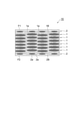
- FIG. 1 is a cross-sectional view schematically showing an embodiment of the organic core material according to the present disclosure.
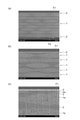
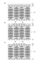
- 2 (a) to 2 (c) are SEM photographs showing an enlarged cross section of the organic core material according to the embodiment of the present disclosure.
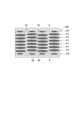
- FIG. 3 is a cross-sectional view schematically showing a state in which a metal foil is arranged on the surface of a laminate containing the first and second prepregs.
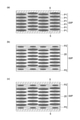
- 4 (a) to 4 (c) are cross-sectional views schematically showing a manufacturing process of the organic core material shown in FIG. 1.
- 5 (a) to 5 (c) are cross-sectional views schematically showing a process of manufacturing a fine wiring board using the organic core material according to the present disclosure.
- FIG. 6 (a) to 6 (c) are cross-sectional views schematically showing a process of manufacturing a fine wiring board using the organic core material according to the present disclosure.
- FIG. 7 is a cross-sectional view schematically showing a fine wiring board manufactured by using the organic core material according to the present disclosure.
- FIG. 1 is a cross-sectional view schematically showing an organic core material according to this embodiment.
- the organic core material 10 shown in FIG. 1 has a laminated structure including a first layer 1 and a second layer 2. That is, the organic core material 10 has a laminated structure including a second layer 2, a plurality of first layers 1, and a second layer 2 in this order.
- FIG. 1 illustrates an embodiment in which the first layer 1 is 6 layers, the number of layers of the first layer 1 is not limited to 6 layers.
- the second layer 2 constituting the surfaces F1 and F2 of the organic core material 10 may not be a single layer, but may be a plurality of layers, respectively.
- the thickness of the organic core material 10 is, for example, 500 to 1600 ⁇ m, and may be 600 to 1400 ⁇ m. When the thickness is 500 ⁇ m or more, the warp of the organic core material 10 is suppressed and the handleability tends to be good. On the other hand, when the thickness is 1600 ⁇ m or less, it tends to be possible to suppress the deterioration of handleability due to the weight.
- the thickness of the organic core material 10 can be adjusted by, for example, the number of layers of the first layer 1 or may be adjusted by the number of layers of the second layer 2.
- the width of the organic core material 10 is, for example, 200 to 1300 mm from the viewpoint of productivity.
- the first layer 1 has a first fiber cloth 1a and a first resin layer 1B composed of a first resin component and in which the first fiber cloth 1a is embedded.
- the second layer 2 has a second fiber cloth 2a and a second resin layer 2B composed of a second resin component and in which the second fiber cloth 2a is embedded.
- the fiber cloths 1a and 2a are composed of weft threads (wavy lines in FIG. 1) and warp threads (ellipses in FIG. 1).
- the second layer 2 is richer in resin component than the first layer 1. That is, the content of the second resin component based on the mass of the second layer is higher than the content of the first resin component based on the mass of the first layer.
- the first layer 1 is a cured prepreg P1
- the second layer 2 is a cured prepreg P2 (see FIG. 3).
- a prepreg P2 richer in resin component than prepreg P1 may be used.
- a prepreg P2 having a relatively thick second resin layer 2b may be used, or a second fiber cloth may be used.
- a prepreg P2 having a relatively thin 2a may be used.
- the alternate long and short dash line in FIG. 1 indicates the boundary between layers.
- FIG. 2A is an SEM photograph showing the entire configuration in the thickness direction from the surface F1 to the surface F2 of the organic core material.
- FIG. 2 (b) is an SEM photograph showing the surface F1 side enlarged from FIG. 2 (a)
- FIG. 2 (c) is an SEM photograph showing the surface F1 side enlarged from FIG. 2 (b).
- a second layer 2 (cured body of the second prepreg) is arranged in the vicinity of the surfaces F1 and F2, respectively, and eight layers of the first layer 1 (cured body of the first prepreg) are arranged between them. ing. It should be noted that the resin components of the adjacent prepregs are often integrated after curing, and the boundary between the two may not be grasped even by observing with an SEM photograph.
- FIGS. 2 (a) and 2 (c) show an example in which a fiber cloth 2a thinner than the fiber cloth 1a arranged in the center of the organic core material is arranged near the surface of the organic core material. It shows.
- the fiber cloths 1a and 2a are, for example, woven fabrics or non-woven fabrics containing inorganic fibers.
- the fibers constituting the fiber cloth natural fibers such as paper and cotton linter; inorganic fibers such as glass fiber and asbestos; organic fibers such as aramid, polyimide, polyvinyl alcohol, polyester, tetrafluoroethylene and acrylic; and a mixture thereof are used.
- glass fiber is preferable from the viewpoint of flame retardancy.
- the glass fiber include a woven cloth using E glass, C glass, D glass, S glass and the like, a glass woven cloth in which short fibers are bonded with an organic binder; and a mixture of glass fiber and cellulose fiber. More preferably, it is a glass woven fabric using E glass. It may be glass fiber, carbon fiber or a combination thereof.
- the fiber cloth has the shape of, for example, a woven fabric, a non-woven fabric, a robink, a chopped strand mat, a surfaced mat, or the like.
- the material and shape are selected according to the intended use or performance of the molded product, and one type may be used alone, or two or more types of materials and shapes may be combined, if necessary.
- the thickness of the fiber cloths 1a and 2a is, for example, 0.01 to 0.5 mm, and from the viewpoint of formability and enabling high-density wiring, 0.015 to 0.2 mm or 0.02 to 0.15 mm. May be. From the viewpoint of heat resistance, moisture resistance, processability, etc., the fiber cloth is preferably surface-treated with a silane coupling agent or the like, or mechanically opened.
- the first and second resin layers 1B and 2B are made of a cured product of a thermosetting resin composition. These layers contain organic components and optionally inorganic components (eg, inorganic fillers) as resin components. In the layers 1 and 2, the components excluding the inorganic fiber component (fiber cloth) can be regarded as the resin component.
- the content of the resin component in the first layer 1 may be 20 to 90% by mass with respect to the mass of the first layer 1, or 20 to 80% by mass from the viewpoint of reducing the linear expansion coefficient. It may be 30 to 90% by mass from the viewpoint of reducing voids after lamination, and may be 40 to 90% by mass from the viewpoint of further improving the flatness of the substrate material.
- the second layer 2 is richer in resin component than the first layer 1. That is, the content of the resin component in the second layer 2 may be 60 to 95% by mass with respect to the mass of the second layer 2, and is 60 to 80% by mass from the viewpoint of reducing the linear expansion coefficient. It may be 65 to 95% by mass from the viewpoint of reducing voids after lamination, and may be 70 to 95% by mass from the viewpoint of further improving the flatness of the substrate material.
- the content of organic components in layers 1 and 2 can be calculated by a method such as ash content measurement.
- the ash content measurement is a method of calculating the ratio of the organic component in the resin component by carbonizing the organic component at a high temperature.
- An example of an inorganic component is an inorganic filler.
- the components excluding the inorganic filler may be regarded as resin components.
- the mass ratio of the resin component contained in the layers 1 and 2 can be calculated from the microscopic image of the cross section of the organic core material 10.
- the image of the cross section is binarized, and the area ratio of the fiber cloths 1a and 2a and the resin layers 1b and 2b is calculated.
- the area ratio is calculated as the volume ratio.
- the mass ratio can be calculated by multiplying the volume ratios of the fiber cloths 1a and 2a and the resin layers 1b and 2b by the specific weights of the fiber cloths 1a and 2a and the resin layers 1b and 2b, respectively.
- the mass ratio of the resin component is calculated from the mass ratio.
- a method for calculating the mass ratio of the resin component will be described for a prepreg in which the fiber cloth is a glass cloth and the resin layer uses a resin component containing an epoxy resin and molten silica as main components.
- the specific gravity of the glass cloth is about 2 to 3 g / cm 3
- the specific gravity of the epoxy resin and the resin containing molten silica as a main component is about 0.8 to 2.5 g / cm 3 .
- the mass ratio of the resin component is calculated from the mass ratio, it is about 29% by mass to about 65% by mass.
- the mass ratio of the resin component For a prepreg using a glass cloth having a specific gravity of 2.6 g / cm 3 for a fiber cloth, an epoxy resin having a specific gravity of 1.8 g / cm 3 for a resin component, and a resin component containing molten silica as a main component, the mass ratio of the resin component.
- the ratio of the area of the resin component to the total cross-sectional area of the prepreg is 69% or more, the mass ratio of the resin component is 60% by mass or more.
- the organic core material 10 Since the second layer 2 rich in the resin component is arranged near the surface of the organic core material 10, the organic core material 10 has sufficiently flat surfaces F1 and F2.
- the organic core material 10 is useful for achieving a higher density and higher reliability of a semiconductor package.
- the flatness of the surface of the organic core material 10 can be evaluated by measuring the thickness of the organic core material 10 at a plurality of different positions and measuring the standard deviation thereof.
- the standard deviation of the thickness of the organic core material 10 may be 4 ⁇ m or less, 3.5 ⁇ m or less, 3 ⁇ m or less, 2.5 ⁇ m or less, 2 ⁇ m or less, or 0.1 ⁇ m or more.
- the standard deviation of the thickness of the organic core material 10 is the value ⁇ calculated by the following formula from the thicknesses T 1 , T 2 , ..., T n of the organic core material 10 at any n positions. There may be.
- the position where the thickness of the organic core material 10 is measured can be selected, for example, by dividing the entire main surface of the organic core material 10 into a plurality of regions having an area of 2500 mm 2 and selecting one or more from each region. The entire main surface of the organic core material 10 is divided so that the number of the plurality of regions having an area of 2500 mm 2 is maximized.
- the thickness is measured, for example, using a micrometer.
- the standard deviation of the thickness at four points corresponding to the vertices of a square having a side of 50 mm is, for example, 3.5 ⁇ m or less, and 3 ⁇ m or less, 2.5 ⁇ m or less, or 2 ⁇ m or less.
- the standard deviation of the thickness at the four points corresponding to the vertices of a square having a side of 70 mm is, for example, 5.0 ⁇ m or less, 4.5 ⁇ m or less, 4.0 ⁇ m or less, or 3.6 ⁇ m or less, and 0. It may be 1 ⁇ m or more.
- the prepreg is produced, for example, by impregnating a thermosetting resin composition with a fiber cloth and then subjecting it to a heat treatment.
- a film of a thermosetting resin composition may be prepared in advance, a fiber cloth may be sandwiched between a pair of films, and then heat treatment may be performed to produce a prepreg.
- the thermosetting resin composition is B-staged.
- the prepreg is preferably subjected to a cooling step for cooling the prepreg.
- the prepreg may be cooled by natural cooling, or may be cooled by using a cooling device such as a blower or a cooling roll.
- the temperature of the prepreg after cooling is usually 5 to 80 ° C, preferably 8 to 50 ° C, more preferably 10 to 30 ° C, and even more preferably room temperature.
- the thickness of one prepreg is not particularly limited, but is preferably 20 to 150 ⁇ m, more preferably 60 to 120 ⁇ m, for example.
- thermosetting resin contained in the thermosetting resin composition examples include epoxy resin, phenol resin, unsaturated imide resin, cyanate resin, isocyanate resin, benzoxazine resin, oxetane resin, unsaturated polyester resin, and allyl resin. , Dicyclopentadiene resin, silicone resin, modified silicone resin, triazine resin, melamine resin, urea resin, furan resin and the like. Further, without being particularly limited to these, known thermosetting resins can be used. These may be used alone or in combination of two or more. Among these, epoxy resin, unsaturated imide resin, and modified silicone resin are preferable.
- the epoxy resin is not particularly limited, but for example, bisphenol type epoxy resin such as bisphenol A type epoxy resin, bisphenol F type epoxy resin, bisphenol S type epoxy resin; alicyclic epoxy resin; aliphatic chain.
- Epoxy resin Novolak type epoxy resin such as phenol novolak type epoxy resin, cresol novolak type epoxy resin, bisphenol A novolak type epoxy resin, bisphenol F novolak type epoxy resin; phenol aralkyl type epoxy resin; stillben type epoxy resin; dicyclopentadiene Type epoxy resin; naphthalen skeleton-containing epoxy resin such as naphthol novolac type epoxy resin and naphthol aralkyl type epoxy resin; biphenyl type epoxy resin; biphenyl aralkyl type epoxy resin; xylylene type epoxy resin; dihydroanthracene type epoxy resin and the like. From these, a naphthalene skeleton-containing epoxy resin may be selected, or a naphthol aralkyl type epoxy resin may
- the unsaturated imide resin examples include a maleimide resin, an addition reaction product of a maleimide resin and a monoamine compound, and a reaction product of a maleimide resin, a monoamine compound, and a diamine compound.
- the maleimide compound is not particularly limited, and is, for example, bis (4-maleimidephenyl) methane, polyphenylmethane maleimide, bis (4-maleimidephenyl) ether, 3,3'-dimethyl-5,5.
- a monoamine compound having an acidic substituent for example, a hydroxyl group, a carboxy group, etc.
- an acidic substituent for example, a hydroxyl group, a carboxy group, etc.
- o-aminophenol for example, a hydroxyl group, a carboxy group, etc.
- M-aminobenzoic acid, p-aminobenzoic acid, o-aminobenzenesulfonic acid, m-aminobenzenesulfonic acid, p-aminobenzenesulfonic acid 3,5-dihydroxyaniline, 3,5-dicarboxyaniline, etc.
- diamine compound a diamine compound having at least two benzene rings is preferable, and a diamine compound having at least two benzene rings linearly between two amino groups is more preferable, and 4,4'-diamino.
- unsaturated imide resin for example, the maleimide compound described in JP-A-2018-165340 can also be used.
- the resin layers 1b and 2b include a curing agent, a curing accelerator, an inorganic filler, an organic filler, a coupling agent, a leveling agent, an antioxidant, a flame retardant, and the like, if necessary. It is preferable to contain at least one selected from a flame retardant aid, a rocking modifier, a thickener, a thixotropic agent, a flexible material, a surfactant, a photopolymerization initiator and the like.
- the thickness accuracy can be improved without high filling, so that the content of the inorganic filler can be, for example, 10 to 60% by volume.
- the upper limit value may be 70% by volume or 80% by volume.
- modified silicone compound modified silicone resin
- thermosetting resins curing agents, curing accelerators, inorganic fillers, heat.
- Thermosetting containing at least one selected from the group consisting of plastic resins, elastomers, organic fillers, flame retardants, ultraviolet absorbers, antioxidants, photopolymerization initiators, fluorescent whitening agents, adhesion improvers and the like.
- a sex resin composition or the like can also be used.
- both terminal amino-modified silicone compounds are preferable, specifically, (A) siloxane diamine represented by the following general formula (1), and (B) at least two N-substituted maleimides in the molecular structure.
- a maleimide compound having a group (C) a two-terminal amino-modified silicone compound obtained by reacting an amine compound having an acidic substituent represented by the following general formula (2), the details of which are described in International Publication No. 2012/099133. It's a street.
- the plurality of R 1s independently represent an alkyl group, a phenyl group or a substituted phenyl group, and may be the same or different from each other
- the plurality of R 2s independently represent an alkyl group and a phenyl group, respectively. It represents a group or a substituted phenyl group and may be the same or different from each other
- R 3 and R 4 independently represent an alkyl group, a phenyl group or a substituted phenyl group, respectively
- R 5 and R 6 are independently divalent. Indicates an organic group.
- n represents an integer of 2 to 50.
- each independently indicates a hydroxyl group, a carboxyl group or a sulfonic acid group
- x is an integer of 1 to 5
- y is an integer of 0 to 4
- x + y 5.
- the manufacturing method according to this embodiment includes the following steps. (A1) Step of preparing a plurality of first prepregs P1 (B1) Step of preparing at least two second prepregs P2 (C1) A second prepreg P2, a plurality of first prepregs P1, and a first A step of heating while applying a pressing force in the thickness direction of the laminated body 10P provided with the second prepreg P2 in this order.
- FIG. 3 is a cross-sectional view schematically showing a state in which a metal foil is arranged on the surface of a laminated body containing prepregs P1 and P2.
- the first prepreg P1 has a first fiber cloth 1a and a first resin layer 1b composed of a first resin component and in which the first fiber cloth 1a is embedded.
- the second prepreg P2 has a second fiber cloth 2a and a second resin layer 2b composed of a second resin component and in which the second fiber cloth 2a is embedded.
- the second prepreg P2 is richer in resin component than the first prepreg P1.
- the first prepreg P1 is cured to form the first layer 1.
- the second prepreg P2 is cured to form the second layer 2.
- the hot pressing step of the step (C1) is carried out using, for example, a multi-stage press, a multi-stage vacuum press, continuous forming, or an autoclave forming machine.
- the metal leaf 5 may be arranged on the surface of the laminated body 10P, respectively.
- the hot press temperature is, for example, 100 to 250 ° C.
- the heating and pressurizing time after the temperature rise is, for example, 0.1 to 5 hours.
- the organic core material after heating and pressurization may be further heated if necessary.
- the laminate 10P is continuously pressurized from the temperature rise to the heating and pressurization at the hot press temperature.
- the pressure applied to the laminated body 10P from the temperature rise to the heating and pressurization at the hot press temperature may be, for example, 0.2 to 10 MPa.
- the metal foil 5 is etched to obtain the organic core material 10.
- the metal leaf 5 can be removed by etching using, for example, ferric chloride solution, ammonium persulfate, or the like.
- this manufacturing method includes the following steps.
- (A2) Step of preparing a plurality of first prepregs P1 (B2) Step of preparing at least two second prepregs P2 (C2) Laminated body 20P (first laminate) composed of a plurality of first prepregs P1.
- Step of heating while applying a pressing force in the thickness direction of the body) (D2) A laminated body 30P (second laminated body) including a second prepreg P2, a laminated body 20P, and a second prepreg P2 in this order. ) The process of heating while applying pressing force in the thickness direction
- the heat pressing step of the step (C2) may be carried out in a state where the metal foils 5 are arranged on both sides of the laminated body 20P. Then, after etching the metal foil 5, the second prepreg P2 is arranged on the surface of the laminated body 20 (the cured body of the laminated body 20P) (see FIG. 4B). Further, the metal foil 5 is arranged on the surface of the second prepreg P2 (see FIG. 4 (c)). In the step (D2), a hot pressing step is carried out on the laminated body P30. Then, by etching the metal foil 5, the organic core material 10 is obtained.
- the step (D2) is carried out under conditions suitable for the curing treatment of the second prepreg P2. It is possible to further suppress the surface waviness of the organic core material 10.
- the metal foil 5 on the surface of the organic core material 10 may not be etched, and the metal foil 5 may be subjected to circuit processing to manufacture a printed wiring board.
- the metal of the metal foil 5 may be copper, gold, silver, nickel, platinum, molybdenum, ruthenium, aluminum, tungsten, iron, titanium, chromium, or at least one of these metal elements from the viewpoint of conductivity.
- the alloy containing the alloy is preferable, copper and aluminum are more preferable, and copper is more preferable.
- circuit processing for example, after forming a resist pattern on the surface of the metal foil, removing the unnecessary metal foil by etching, peeling the resist pattern, and then drilling. This can be done by forming the necessary through holes, forming the resist pattern again, applying plating to make the through holes conductive, and finally peeling off the resist pattern.
- a semiconductor package can be manufactured by mounting a semiconductor chip, memory, etc. at a predetermined position on a printed wiring board. Since the semiconductor package using the organic core material of the present embodiment has a small variation in thickness, the yield at the time of mounting the semiconductor chip tends to be improved.
- a build-up film layer can be formed on the printed wiring board. Circuit patterns can be formed on the printed wiring board or on the build-up film layer.
- a subtractive method a full additive method, a semi-additive method (SAP: Semi Adaptive Process), a modified semi-additive method (m-SAP: modified Semi Adaptive Process), or the like can be used (see FIGS. 5 to 7). ..
- a prepreg was prepared according to the following procedure.
- 24 g of silicone diamine (trade name "KF-8010", manufactured by Shinetsu Silicone)
- 240 g of bis (4-maleimidephenyl) methane 240 g
- propylene glycol monomethyl ether 400 g
- the mixture was charged and reacted at 115 ° C. for 4 hours, then heated to 130 ° C. and concentrated under normal pressure to obtain a solution having a resin content of 60% by mass.
- the obtained varnish was impregnated and coated on E glass having a thickness of 0.1 mm by adjusting the gap, and dried by heating at 150 ° C. for 10 minutes to prepare a prepreg having a resin content of 50% by mass. Further, the obtained varnish was impregnated and coated on E glass having a thickness of 0.015 mm by adjusting the gap, and dried by heating at 150 ° C. for 10 minutes to prepare a prepreg having a resin content of 70% by mass.
- the resin content of the prepreg contained all the components other than the glass cloth constituting the prepreg, and was calculated including the components of the silica slurry.
- the measurement of the mass ratio of the resin content was calculated by dividing the difference between the masses of the prepreg and the glass cloth by the mass of the prepreg. The adjustment of the gap width during the impregnation coating was repeated until the prepregs having the mass ratios of the resin components of 50% by mass and 70% by mass were obtained.
- Stainless steel plate (thickness 1.8 mm), 270 mm square size copper foil on the outside (thickness 5 ⁇ m, manufactured by Mitsui Mining & Smelting Co., Ltd.), and 265 mm square size cushion material on the outside (thickness 0.2 mm, Oji)
- Five sheets of paper, KS190), and 260 mm square copper foil (thickness 12 ⁇ m, manufactured by Mitsui Mining & Smelting Co., Ltd.) are placed on both sides, and a press device (manufactured by Meiki Seisakusho, MHPC-VF-350) is placed.
- the obtained organic core material was immersed in an aqueous solution of ammonium persulfate to etch the copper foil (see FIG. 4 (b)).
- One prepreg having a 250 mm square size resin content of 70% by mass was placed on the upper surface and the lower surface of the etched organic core material.
- a 270 mm square size copper foil was placed outside the prepreg having a resin component mass ratio of 70 mass% (see FIG. 4 (c)).
- Five cushioning materials were placed, and 260 mm square copper foil (thickness 12 ⁇ m, made by Mitsui Mining & Smelting Co., Ltd.) was placed on both sides.
- the holding time at a pressure of 3 MPa, a vacuum degree of 40 hPa, a temperature rise rate of 4 ° C./min, and a temperature of 240 ° C. is 85.
- An organic core material was obtained through a step of heating and pressurizing under the condition of minutes.
- Examples 3 and 4 After producing the prepreg in the same manner as in Example 1, the mass ratio of the resin content of 250 mm square size is 70% by mass on the upper surface and the lower surface of the prepreg having the mass ratio of the resin content of 250 mm square size of 6 stacked. The prepregs of were placed one by one. A 270 mm square size copper foil (thickness 5 ⁇ m, manufactured by Mitsui Mining & Smelting Co., Ltd.) was placed outside the prepreg having a resin content of 70% by mass (see FIG. 3).
- Five cushioning materials were placed, and 260 mm square copper foil (thickness 12 ⁇ m, made by Mitsui Mining & Smelting Co., Ltd.) was placed on both sides.
- the holding time at a pressure of 3 MPa, a vacuum degree of 40 hPa, a temperature rise rate of 4 ° C./min, and a temperature of 240 ° C. is 85.
- An organic core material was obtained through a step of heating and pressurizing under the condition of minutes.
- the organic core material obtained by the above method was evaluated according to the following evaluation method. The results are shown in Table 1.
- ⁇ Calculation of standard deviation of thickness of 50 mm square size The range of 150 mm square size at the center of the organic core material of 250 mm square size (square with a side of 250 mm in a plan view) was divided into 9 areas of 50 mm square, and the standard deviation value of the thickness of 9 areas was calculated. In the case of a large package for servers, it is assumed that the chip size will be about 50 mm square, and 50 mm square is set within the standard deviation calculation range. The outside of the center 150 mm square size was not used for evaluation because the resin contained in the prepreg flowed out to the outside of the prepreg and the organic core material became thin.
- the thickness of four points at the four corners of a 50 mm square area was measured.
- the standard deviation value was calculated using the thickness values of the four points as the population.
- the maximum value among the standard deviation values calculated from the nine areas is shown in Table 1 as the standard deviation value of each organic core material.
- ⁇ Calculation of thickness standard deviation of 70 mm square size The range of 140 mm square size at the center of the organic core material of 250 mm square size (square with a side of 250 mm in a plan view) was divided into four areas of 70 mm square, and the standard deviation values of the thicknesses of the four areas were calculated. Since the UV irradiation range at the time of forming the photoresist pattern in the copper wiring forming step is 70 mm square, 70 mm square was set as the range for calculating the standard deviation. Using a micrometer, the thickness of four points at the four corners of the 70 mm square area was measured. The standard deviation value was calculated using the thickness values of the four points as the population. The maximum value among the standard deviation values calculated from the four areas is shown in Table 1 as the standard deviation value of each organic core material.
- An organic core material having a size of 250 mm square (a square having a side of 250 mm in a plan view) was prepared.
- the central region (range of 150 mm square size) of this organic core material was cut into a 30 mm square size with a cutting machine.
- Refine Saw Excel A (manufactured by Refine Tech Co., Ltd.) was used for cutting. After cutting, the substrate surface was washed by immersing it in a 10 mass% sulfuric acid aqueous solution for 1 minute. Then, it was washed with pure water.
- a chip with a solder bump has a structure in which copper pillars are arranged on the surface of a silicon wafer and solders are arranged on an end face different from that of the silicon wafer of the copper pillars. Copper pillars and solder are collectively called solder bumps.
- the size of each configuration was as follows. ⁇ Chip size with solder bump: 25 mm square ⁇ Silicon wafer thickness: 725 ⁇ 25 ⁇ m ⁇ Solder bump pitch: 150 ⁇ m -Copper pillar height: 45 ⁇ m ⁇ Solder bump height: 15 ⁇ m ⁇ Solder diameter: 75 ⁇ m
- Copper wiring was formed in the organic core material by the semi-additive method.
- the copper foil of the organic core material was immersed in an aqueous solution of ammonium persulfate and etched.
- a build-up film manufactured by Ajinomoto Fine-Techno Co., Ltd., GX92
- a vacuum laminator manufactured by Nikko Materials Co., Ltd., V-130
- the conditions were a pressure of 0.5 MPa, a vacuuming time of 15 seconds, a pressurizing time of 60 seconds, and a temperature of 50 ° C.
- a seed layer 16 was formed on the surface of one of the build-up film layers by a sputtering method (FIG. 5 (b)).
- the seed layer 16 has a two-layer structure consisting of a titanium layer of 25 nm and a copper layer of 150 nm.
- a photoresist film (RY-5107UT, manufactured by Hitachi Kasei Co., Ltd.) of the photosensitive resin composition was laminated on the seed layer.
- the conditions were a pressure of 0.5 MPa, a vacuuming time of 15 seconds, a pressurizing time of 60 seconds, and a temperature of 50 ° C.
- the photosensitive resin layer 17 was formed on the surface of the seed layer 16 (FIG. 5 (c)).
- a square area with a side of 70 mm was irradiated with UV to expose it.
- a 1% by mass aqueous solution of sodium carbonate was sprayed and developed using a spin developer (ultra-high pressure spin developer manufactured by Blue Ocean Technology Co., Ltd.).
- a plasma asher AP series batch type plasma processing device manufactured by Nordson Advanced Technology Co., Ltd.
- oxygen plasma was applied to the resist pattern to remove the resist residue during development.
- a copper wiring 18 having a wiring width / space width (L / S) 2 ⁇ m / 2 ⁇ m was formed by an electrolytic copper plating method (FIG. 6 (b)).
- the wiring height was 3 ⁇ m.
- a 2.38% by mass aqueous solution of TMAH (tetramethylammonium hydroxide) was sprayed on a spin developer to peel off the resist (FIG. 6 (c)).
- the seed layer 16 exposed by peeling the resist was removed by etching (FIG. 7).
- the copper layer was removed by immersing it in an aqueous solution of a copper etching solution (manufactured by Mitsubishi Gas Chemical Company, WLC-C2) and pure water at a mass ratio of 1: 1 at 23 ° C.
- the titanium layer was removed by immersing it in an aqueous solution of a titanium etching solution (manufactured by Mitsubishi Gas Chemical Company, WLC-T) and a 23% aqueous ammonia solution at a mass ratio of 50: 1 at 23 ° C. for 65 seconds, and then washing with pure water. ..
- a titanium etching solution manufactured by Mitsubishi Gas Chemical Company, WLC-T
- a 23% aqueous ammonia solution at a mass ratio of 50: 1 at 23 ° C. for 65 seconds
- Wiring yield is 75% or more and 100% or less
- an organic core material useful for achieving a high density and high reliability of a semiconductor package and a method for manufacturing the same are provided.
Landscapes
- Engineering & Computer Science (AREA)
- Chemical & Material Sciences (AREA)
- Textile Engineering (AREA)
- Materials Engineering (AREA)
- Microelectronics & Electronic Packaging (AREA)
- Chemical Kinetics & Catalysis (AREA)
- Health & Medical Sciences (AREA)
- Medicinal Chemistry (AREA)
- Polymers & Plastics (AREA)
- Organic Chemistry (AREA)
- Manufacturing & Machinery (AREA)
- Composite Materials (AREA)
- Mechanical Engineering (AREA)
- Laminated Bodies (AREA)
- Reinforced Plastic Materials (AREA)
Abstract
本開示に係る有機コア材の製造方法は、第一の繊維クロスと、第一の樹脂成分からなり且つ第一の繊維クロスが埋め込まれている第一の樹脂層とをそれぞれ有する複数の第一のプリプレグを準備する工程と、第二の繊維クロスと、第二の樹脂成分からなり且つ第二の繊維クロスが埋め込まれている第二の樹脂層とをそれぞれ有する少なくとも二枚の第二のプリプレグを準備する工程と、第二のプリプレグと、複数の第一のプリプレグと、第二のプリプレグとをこの順序で備える積層体の厚さ方向に押圧力を加えながら加熱する工程とを含み、第二のプリプレグの質量を基準とする第二の樹脂成分の含有率が第一のプリプレグの質量を基準とする第一の樹脂成分の含有率よりも高い。
Description
本開示は有機コア材及びその製造方法に関する。
近年、電子機器の小型化、軽量化及び多機能化が一段と進んでいる。これに伴い、プリント配線板及びLSI(Large Scale Integration)を実装する半導体パッケージに対して高密度化及び高い信頼性が要求されている。特許文献1は、配線層の高密度化を実現するための配線基板を開示している。特許文献2は、優れた接続信頼性を実現するためのプリント配線板及び半導体装置を開示している。
半導体パッケージの高密度化及び高い信頼性をより一層高度に実現するため、有機コア材の厚さ精度に対する要求も厳しくなりつつある。有機コア材の製造に使用されるプリプレグはガラスクロス等の繊維クロスを補強材として含む。特許文献2の段落[0057]には、複数枚のプリプレグを金属箔で挟み込んでプレス成形する工程を経て有機コア材を製造することが記載されている。本発明者らの検討によると、プリプレグ内に存在する繊維クロスにより、プレス成型によって得られる有機コア材の表面にうねりが発生する。この表面うねりは、半導体パッケージの製造において歩留まり低下の原因となり得る。
例えば、有機コア材上に形成した配線層の上に微細なソルダーバンプを持つ半導体チップを実装する際、有機コア材の表面うねりの影響によって、配線とソルダーバンプの接続歩留まりが低下する傾向がある。また、有機コア材上に形成した絶縁層の上にセミアディティブ法(SAP:Semi Additive Process)を用いて配線幅/スペース幅=2/2μm以下の配線を形成する際、表面うねりの影響によって、フォトレジストパターンの形成歩留まりが低下し、配線の歩留まりが低下する傾向がある。配線幅/スペース幅=2/2μmより幅の広い配線を形成する場合であっても、フォトレジストパターンの幅のばらつきに起因して配線幅がばらつき、配線に信号を通した際の伝送損失が増大する傾向がある。
本開示は、半導体パッケージの高密度化及び高い信頼性をより一層高度に実現するのに有用な有機コア材及びその製造方法を提供する。
本開示に係る有機コア材の製造方法においては、少なくとも二種類のプリプレグ(第一及び第二のプリプレグ)を使用する。第一のプリプレグは、第一の繊維クロスと、第一の樹脂成分からなり且つ第一の繊維クロスが埋め込まれている第一の樹脂層とを有する。第二のプリプレグは、第二の繊維クロスと、第二の樹脂成分からなり且つ第二の繊維クロスが埋め込まれている第二の樹脂層とを有する。第二のプリプレグは、第一のプリプレグよりも樹脂成分リッチである。すなわち、第二のプリプレグの質量を基準とする第二の樹脂成分の含有率は、第一のプリプレグの質量を基準とする第一の樹脂成分の含有率よりも高い。第二のプリプレグの質量を基準とする第二の樹脂成分の含有率は、例えば、60質量%以上である。
本開示に係る有機コア材の製造方法の第一態様は、複数の第一のプリプレグを準備する工程と、少なくとも二枚の第二のプリプレグを準備する工程と、第二のプリプレグと、複数の第一のプリプレグと、第二のプリプレグとをこの順序で備える積層体の厚さ方向に押圧力を加えながら加熱する工程(以下、場合により、「熱プレス工程」という。)とを含む。樹脂成分リッチの第二のプリプレグで複数の第一のプリプレグをサンドイッチした状態で熱プレス工程を実施することで、繊維クロスに起因する表面うねりが十分に低減された有機コア材を製造することができる。
本開示に係る有機コア材の製造方法の第二態様は、複数の第一のプリプレグの積層体に対して熱プレス工程を実施した後、この積層体の両表面に第二のプリプレグを配置した状態で熱プレス工程を再度実施するものである。すなわち、この製造方法は、複数の第一のプリプレグを準備する工程と、少なくとも二枚の第二のプリプレグを準備する工程と、複数の第一のプリプレグの第一の積層体の厚さ方向に押圧力を加えながら加熱する工程と、第二のプリプレグと、第一の積層体と、第二のプリプレグとをこの順序で備える第二の積層体の厚さ方向に押圧力を加えながら加熱する工程とを含む。樹脂成分リッチの第二のプリプレグで第一の積層体をサンドイッチした状態で熱プレス工程を実施することで、繊維クロスに起因する表面うねりが十分に低減された有機コア材を製造することができる。
これらの製造方法によれば、十分に平坦な表面を有する有機コア材を製造することができる。かかる有機コアを使用することで、高い精度で微細配線を形成することができる。有機コアの表面が十分に平坦であることは、有機コアの厚さを複数点において測定し、測定値の標準偏差が十分に小さいことで示すことができる。本開示に係る有機コア材は、平面視において一辺50mmの正方形の頂点に相当する4点における厚さの標準偏差が例えば3.5μm以下である。
本開示に係る有機コア材の第一態様は、第一の層と第二の層とを含む積層構造を有する。第一の層は、第一の繊維クロスと、第一の樹脂成分からなり且つ第一の繊維クロスが埋め込まれている第一の樹脂層とを有する。第二の層は、第二の繊維クロスと、第二の樹脂成分からなり且つ第二の繊維クロスが埋め込まれている第二の樹脂層とを有する。第二の層は、第一の層よりも樹脂成分リッチである。第一態様に係る有機コア材は、第二の層と、複数の第一の層と、第二の層とをこの順序で備える積層構造を有し、第二の層の質量を基準とする第二の樹脂成分の含有率が第一の層の質量を基準とする第一の樹脂成分の含有率よりも高い。
有機コア材の表面近傍に樹脂成分リッチの第二の層が配置されていることで、有機コア材は十分に平坦な表面を有する。かかる有機コアは半導体パッケージの高密度化及び高い信頼性をより一層高度に実現するのに有用である。
本開示に係る有機コア材の第二態様は、縦断面において繊維クロスと樹脂層が交互に配置されており、平面視において一辺50mmの正方形の頂点に相当する4点における厚さの標準偏差が3.5μm以下である。この有機コア材の縦断面において、有機コア材の表面近傍に、例えば、有機コア材の中央部に配置された繊維クロスよりも薄い繊維クロスが配置されていている(図2(c)参照)。有機コア材の表面近傍に、薄い繊維クロスが配置されていることで、繊維クロスに起因する表面うねりを抑制することができる。平坦な表面を有する有機コアは半導体パッケージの高密度化及び高い信頼性をより一層高度に実現するのに有用である。
本開示によれば、半導体パッケージの高密度化及び高い信頼性をより一層高度に実現するのに有用な有機コア材及びその製造方法が提供される。
以下、本開示のいくつかの実施形態について詳細に説明する。ただし、本発明は以下の実施形態に限定されるものではない。
<有機コア材>
図1は、本実施形態に係る有機コア材を模式的に示す断面図である。図1に示される有機コア材10は、第一の層1と第二の層2とを含む積層構造を有する。すなわち、有機コア材10は、第二の層2と、複数の第一の層1と、第二の層2とをこの順序で備える積層構造を有する。なお、図1には第一の層1が6層である態様を図示したが、第一の層1の層数は6層に限定されるものではない。また、有機コア材10の表面F1,F2を構成する第二の層2はそれぞれ単層でなくてもよく、それぞれ複数の層であってもよい。
図1は、本実施形態に係る有機コア材を模式的に示す断面図である。図1に示される有機コア材10は、第一の層1と第二の層2とを含む積層構造を有する。すなわち、有機コア材10は、第二の層2と、複数の第一の層1と、第二の層2とをこの順序で備える積層構造を有する。なお、図1には第一の層1が6層である態様を図示したが、第一の層1の層数は6層に限定されるものではない。また、有機コア材10の表面F1,F2を構成する第二の層2はそれぞれ単層でなくてもよく、それぞれ複数の層であってもよい。
有機コア材10の厚さは、例えば、500~1600μmであり、600~1400μmであってもよい。厚さが500μm以上であることで、有機コア材10の反りが抑制されてハンドリング性が良好となる傾向がある。他方、厚さが1600μm以下であることで重さに起因してハンドリング性が悪化することを抑制できる傾向にある。有機コア材10の厚さは、例えば、第一の層1の層数によって調整することができ、第二の層2の層数によって調整してもよい。有機コア材10の幅は、生産性の観点から、例えば、200~1300mmである。
第一の層1は、第一の繊維クロス1aと、第一の樹脂成分からなり且つ第一の繊維クロス1aが埋め込まれている第一の樹脂層1Bとを有する。第二の層2は、第二の繊維クロス2aと、第二の樹脂成分からなり且つ第二の繊維クロス2aが埋め込まれている第二の樹脂層2Bとを有する。なお、繊維クロス1a,2aは横糸(図1における波線)と縦糸(図1における楕円)とによって構成されている。第二の層2は、第一の層1よりも樹脂成分リッチである。すなわち、第二の層の質量を基準とする第二の樹脂成分の含有率が第一の層の質量を基準とする第一の樹脂成分の含有率よりも高い。
第一の層1はプリプレグP1が硬化したものであり、第二の層2はプリプレグP2が硬化したものである(図3参照)。第二の層2が第一の層1よりも樹脂成分リッチな状態とするには、プリプレグP2としてプリプレグP1よりも樹脂成分リッチなものを使用すればよい。第二の層2が第一の層1と比較して樹脂成分リッチとするには、例えば、第二の樹脂層2bが比較的厚いプリプレグP2を使用してもよいし、第二の繊維クロス2aが比較的薄いプリプレグP2を使用してもよい。図1における一点鎖線は層の境界を示している。
図2(a)~図2(c)は本実施形態に係る有機コア材の断面を拡大して示すSEM写真である。図2(a)は有機コア材の表面F1から表面F2にわたる厚さ方向の全体の構成を示すSEM写真である。図2(b)は、表面F1側を図2(a)よりも拡大して示すSEM写真であり、図2(c)は図2(b)よりも拡大して示すSEM写真である。表面F1,F2の近傍にそれぞれ第二の層2(第二のプリプレグの硬化体)が配置され、これらの間に8層の第一の層1(第一のプリプレグの硬化体)が配置されている。なお、隣接するプリプレグ同士は硬化後においては樹脂成分が一体化することが多く、SEM写真で観察しても両者の境界を把握できない場合がある。
一方、SEMによる縦断面の観察により、樹脂層3と繊維クロス(繊維クロス1a,2a)が交互に配置されていることを確認することができる。図2(a)~図2(c)に示すSEM写真は、有機コア材の表面近傍に、有機コア材の中央部に配置された繊維クロス1aよりも薄い繊維クロス2aが配置された例を示すものである。有機コア材の表面近傍に、薄い繊維クロスを含むプリプレグの硬化体が配置されていることで、繊維クロスに起因する表面うねりを抑制することができる。
繊維クロス1a,2aは、例えば、無機繊維を含む織布又は不織布である。繊維クロスを構成する繊維として、紙、コットンリンター等の天然繊維;ガラス繊維及びアスベスト等の無機繊維;アラミド、ポリイミド、ポリビニルアルコール、ポリエステル、テトラフルオロエチレン及びアクリル等の有機繊維;これらの混合物などが挙げられる。これらの中でも、難燃性の観点から、ガラス繊維が好ましい。ガラス繊維としては、Eガラス、Cガラス、Dガラス、Sガラス等を用いた織布又は短繊維を有機バインダーで接着したガラス織布;ガラス繊維とセルロース繊維とを混抄したもの等が挙げられる。より好ましくは、Eガラスを使用したガラス織布である。ガラス繊維、炭素繊維又はこれらの組み合わせであってもよい。
繊維クロスは、例えば、織布、不織布、ロービンク、チョップドストランドマット又はサーフェシングマット等の形状を有するものである。なお、材質及び形状は、目的とする成形物の用途又は性能により選択され、1種を単独で使用してもよいし、必要に応じて、2種以上の材質及び形状を組み合わせることもできる。
繊維クロス1a,2aの厚さは、例えば、0.01~0.5mmであり、成形性及び高密度配線を可能にする観点から、0.015~0.2mm又は0.02~0.15mmであってもよい。繊維クロスは、耐熱性、耐湿性、加工性等の観点から、シランカップリング剤等で表面処理したもの、機械的に開繊処理を施したものなどであることが好ましい。
第一及び第二の樹脂層1B,2B(樹脂層3)は熱硬化性樹脂組成物の硬化物からなる。これらの層は、樹脂成分として、有機成分及び必要に応じて無機成分(例えば、無機フィラー)を含む。層1,2において、無機繊維成分(繊維クロス)を除いた成分を樹脂成分とみなすことができる。
第一の層1における樹脂成分の含有率は、第一の層1の質量に対して20~90質量%であってもよく、線膨張係数低減の観点から20~80質量%であってもよく、積層後のボイド低減の観点から30~90質量%であってもよく、基板材料の平坦性のより一層の向上の観点から40~90質量%であってもよい。一方、上述のとおり、第二の層2は第一の層1よりも樹脂成分リッチである。すなわち、第二の層2における樹脂成分の含有率は、第二の層2の質量に対して60~95質量%であってもよく、線膨張係数低減の観点から60~80質量%であってもよく、積層後のボイド低減の観点から65~95質量%であってもよく、基板材料の平坦性のより一層の向上の観点から70~95質量%であってもよい。
層1,2における有機成分の含有率は、灰分測定等の方法で算出できる。灰分測定は、有機成分を高温で炭化することにより、樹脂成分中の有機成分の割合を算出する方法である。無機成分の例は無機フィラーである。層1,2において、無機フィラーを除いた成分を樹脂成分とみなしてもよい。
層1,2に含まれる樹脂成分の質量割合は、有機コア材10の断面の顕微鏡画像から算出することができる。断面の画像を二値化処理し、繊維クロス1a,2a及び樹脂層1b,2bの面積比を算出する。面積比は体積比として計算する。繊維クロス1a,2a及び樹脂層1b,2bの体積比に、繊維クロス1a,2a及び樹脂層1b,2bのそれぞれの比重を掛け積算することで、質量比を算出できる。質量比から樹脂成分の質量割合を算出する。
例えば、繊維クロスがガラスクロスであり、樹脂層がエポキシ樹脂及び溶融シリカを主成分とした樹脂成分を用いたプリプレグについて、樹脂成分の質量割合の算出方法を説明する。ガラスクロスの比重は約2~3g/cm3、エポキシ樹脂及び溶融シリカを主成分とした樹脂の比重は約0.8~2.5g/cm3である。ガラスクロスと樹脂成分の面積比が4:6の場合、ガラスクロスと樹脂成分の質量比はガラスクロス:樹脂成分=4×3:6×0.8=25:10からガラスクロス:樹脂分=4×2:6×2.5=5:10の間となる。質量比から樹脂成分の質量割合を算出すると約29質量%~約65質量%となる。
例えば、繊維クロスに比重2.6g/cm3のガラスクロス、樹脂成分に比重1.8g/cm3のエポキシ樹脂及び溶融シリカを主成分とした樹脂成分を用いたプリプレグについて、樹脂成分の質量割合を算出する場合、プリプレグの断面積全体に占める樹脂分の面積の割合が69%以上のとき、樹脂成分の質量割合は60質量%以上となる。
有機コア材10の表面近傍に樹脂成分リッチの第二の層2が配置されていることで、有機コア材10は十分に平坦な表面F1,F2を有する。有機コア材10は半導体パッケージの高密度化及び高い信頼性をより一層高度に実現するのに有用である。有機コア材10の表面の平坦性は、有機コア材10の厚さを異なる複数の位置で測定し、その標準偏差で評価することができる。有機コア材10の厚さの標準偏差は4μm以下、3.5μm以下、3μm以下、2.5μm以下又は2μm以下であってもよく、0.1μm以上であってもよい。有機コア材10の厚さの標準偏差は、任意のn個の位置それぞれにおける有機コア材10の厚さT1、T2、・・・、Tnから、下記式によって算出される値σであってもよい。

有機コア材10の厚さが測定される位置は、例えば、有機コア材10の主面全体を2500mm2の面積を有する複数の領域に分割し、各領域から1個以上選択することができる。2500mm2の面積を有する複数の領域の数が最大になるように、有機コア材10の主面全体が分割される。厚さは例えばマイクロメータを用いて測定される。例えば、有機コア材10の平面視において、一辺50mmの正方形の頂点に相当する4点における厚さの標準偏差は、例えば、3.5μm以下であり、3μm以下、2.5μm以下又は2μm以下であってもよく、0.1μm以上であってもよい。一辺70mmの正方形の頂点に相当する4点における厚さの標準偏差は、例えば、5.0μm以下であり、4.5μm以下、4.0μm以下又は3.6μm以下であってもよく、0.1μm以上であってもよい。
(プリプレグ)
プリプレグは、例えば、繊維クロスを熱硬化性樹脂組成物に含浸した後、加熱処理を施すことによって製造される。あるいは、熱硬化性樹脂組成物のフィルムを予め準備し、一対のフィルムで繊維クロスをサンドイッチした後、加熱処理を施すことによってプリプレグを製造してもよい。加熱処理によって、熱硬化性樹脂組成物はB-ステージ化される。プリプレグは、その取扱い性及びタック性の観点から、これを冷却する冷却工程に供することが好ましい。プリプレグの冷却は、自然放冷によって行ってもよく、送風装置、冷却ロール等の冷却装置を用いて行ってもよい。冷却後のプリプレグの温度は、通常、5~80℃であり、8~50℃が好ましく、10~30℃がより好ましく、室温が更に好ましい。一枚のプリプレグの厚さは、特に制限されるものではないが、例えば、20~150μmが好ましく、60~120μmがより好ましい。
プリプレグは、例えば、繊維クロスを熱硬化性樹脂組成物に含浸した後、加熱処理を施すことによって製造される。あるいは、熱硬化性樹脂組成物のフィルムを予め準備し、一対のフィルムで繊維クロスをサンドイッチした後、加熱処理を施すことによってプリプレグを製造してもよい。加熱処理によって、熱硬化性樹脂組成物はB-ステージ化される。プリプレグは、その取扱い性及びタック性の観点から、これを冷却する冷却工程に供することが好ましい。プリプレグの冷却は、自然放冷によって行ってもよく、送風装置、冷却ロール等の冷却装置を用いて行ってもよい。冷却後のプリプレグの温度は、通常、5~80℃であり、8~50℃が好ましく、10~30℃がより好ましく、室温が更に好ましい。一枚のプリプレグの厚さは、特に制限されるものではないが、例えば、20~150μmが好ましく、60~120μmがより好ましい。
上記熱硬化性樹脂組成物に含まれる熱硬化性樹脂としては、例えば、エポキシ樹脂、フェノール樹脂、不飽和イミド樹脂、シアネート樹脂、イソシアネート樹脂、ベンゾオキサジン樹脂、オキセタン樹脂、不飽和ポリエステル樹脂、アリル樹脂、ジシクロペンタジエン樹脂、シリコーン樹脂、変性シリコーン樹脂、トリアジン樹脂、メラミン樹脂、尿素樹脂、フラン樹脂等が挙げられる。また、特にこれらに制限されず、公知の熱硬化性樹脂を使用できる。これらは、1種を単独で使用してもよいし、2種以上を併用することもできる。これらの中でも、エポキシ樹脂、不飽和イミド樹脂、変性シリコーン樹脂が好ましい。
上記エポキシ樹脂としては、特に制限されるものではないが、例えば、ビスフェノールA型エポキシ樹脂、ビスフェノールF型エポキシ樹脂、ビスフェノールS型エポキシ樹脂等のビスフェノール型エポキシ樹脂;脂環式エポキシ樹脂;脂肪族鎖状エポキシ樹脂;フェノールノボラック型エポキシ樹脂、クレゾールノボラック型エポキシ樹脂、ビスフェノールAノボラック型エポキシ樹脂、ビスフェノールFノボラック型エポキシ樹脂等のノボラック型エポキシ樹脂;フェノールアラルキル型エポキシ樹脂;スチルベン型エポキシ樹脂;ジシクロペンタジエン型エポキシ樹脂;ナフトールノボラック型エポキシ樹脂、ナフトールアラルキル型エポキシ樹脂等のナフタレン骨格含有型エポキシ樹脂;ビフェニル型エポキシ樹脂;ビフェニルアラルキル型エポキシ樹脂;キシリレン型エポキシ樹脂;ジヒドロアントラセン型エポキシ樹脂などが挙げられる。これらの中から、ナフタレン骨格含有型エポキシ樹脂を選択してもよく、ナフトールアラルキル型エポキシ樹脂を選択してもよい。
上記不飽和イミド樹脂としては、例えば、マレイミド樹脂、マレイミド樹脂とモノアミン化合物との付加反応物、マレイミド樹脂とモノアミン化合物とジアミン化合物との反応物等が挙げられる。前記マレイミド化合物としては、特に制限されるものではないが、例えば、ビス(4-マレイミドフェニル)メタン、ポリフェニルメタンマレイミド、ビス(4-マレイミドフェニル)エーテル、3,3’-ジメチル-5,5’-ジエチル-4,4’-ジフェニルメタンビスマレイミド、4-メチル-1,3-フェニレンビスマレイミド、m-フェニレンビスマレイミド、ビス(4-マレイミドフェニル)スルホン、ビス(4-マレイミドフェニル)スルフィド、ビス(4-マレイミドフェニル)ケトン、2,2-ビス(4-(4-マレイミドフェノキシ)フェニル)プロパン、ビス(4-(4-マレイミドフェノキシ)フェニル)スルホン、4,4’-ビス(3-マレイミドフェノキシ)ビフェニル、1,6-ビスマレイミド-(2,2,4-トリメチル)ヘキサン等が挙げられる。これらの中から、ビス(4-マレイミドフェニル)メタンを選択してもよい。
上記モノアミン化合物としては、酸性置換基(例えば、水酸基、カルボキシ基等)を有するモノアミン化合物が好ましく、具体的には、o-アミノフェノール、m-アミノフェノール、p-アミノフェノール、o-アミノ安息香酸、m-アミノ安息香酸、p-アミノ安息香酸、o-アミノベンゼンスルホン酸、m-アミノベンゼンスルホン酸、p-アミノベンゼンスルホン酸、3,5-ジヒドロキシアニリン、3,5-ジカルボキシアニリン等が挙げられる。
上記ジアミン化合物としては、少なくとも2個のベンゼン環を有するジアミン化合物が好ましく、2つのアミノ基の間に少なくとも2個のベンゼン環を直鎖状に有するジアミン化合物がより好ましく、4,4’-ジアミノジフェニルメタン、4,4’-ジアミノ-3,3’-ジメチル-ジフェニルメタン、4,4’-ジアミノ-3,3’-ジエチル-ジフェニルメタン、4,4’-ジアミノジフェニルエーテル、4,4’-ジアミノジフェニルスルホン、3,3’-ジアミノジフェニルスルホン、4,4’-ジアミノジフェニルケトン等が挙げられる。
前記不飽和イミド樹脂としては、例えば、特開2018-165340号公報等に記載のマレイミド化合物を使用することもできる。
前記不飽和イミド樹脂としては、例えば、特開2018-165340号公報等に記載のマレイミド化合物を使用することもできる。
樹脂層1b,2bは、上記熱硬化性樹脂の他に、必要に応じて、硬化剤、硬化促進剤、無機充填材、有機充填材、カップリング剤、レベリング剤、酸化防止剤、難燃剤、難燃助剤、揺変性付与剤、増粘剤、チキソ性付与剤、可撓性材料、界面活性剤及び光重合開始材等から選択される少なくとも1つを含有する態様が好ましい。特に、無機充填材については、本実施形態ではこれを高充填しなくとも厚さ精度を高めることができるため、該無機充填材の含有量を例えば10~60体積%にすることができ、20~60体積%にしてもよく、30~60体積%にしてもよく、当該数値範囲においてさらに上限値を57体積%とすることもでき、55体積%とすることもできる。但し、無機充填材を高充填する必要がある場合には、本実施形態においては、無機充填材の含有量が60体積%を超えることを必ずしも否定はせず、例えば前記含有量の数値範囲の上限値を70体積%としてもよいし、80体積%としてもよい。
また、例えば国際公開第2012/099133号に記載されている、変性シリコーン化合物(変性シリコーン樹脂)、必要に応じてさらに、他の熱硬化性樹脂、硬化剤、硬化促進剤、無機充填材、熱可塑性樹脂、エラストマー、有機充填材、難燃剤、紫外線吸収剤、酸化防止剤、光重合開始剤、蛍光増白剤及び接着性向上剤等からなる群から選択される少なくとも1種を含有する熱硬化性樹脂組成物等も用いることができる。
上記変性シリコーン化合物としては、両末端アミノ変性シリコーン化合物が好ましく、具体的には、(A)下記一般式(1)に示すシロキサンジアミン、(B)分子構中に少なくとも2個のN-置換マレイミド基を有するマレイミド化合物、(C)下記一般式(2)に示す酸性置換基を有するアミン化合物を反応させてなる両末端アミノ変性シリコーン化合物であり、詳細は国際公開第2012/099133号に記載の通りである。


<有機コア材の製造方法>
次に、有機コア材10の製造方法について説明する。本実施形態に係る製造方法は以下の工程を含む。
(A1)複数の第一のプリプレグP1を準備する工程
(B1)少なくとも二枚の第二のプリプレグP2を準備する工程
(C1)第二のプリプレグP2と、複数の第一のプリプレグP1と、第二のプリプレグP2とをこの順序で備える積層体10Pの厚さ方向に押圧力を加えながら加熱する工程
次に、有機コア材10の製造方法について説明する。本実施形態に係る製造方法は以下の工程を含む。
(A1)複数の第一のプリプレグP1を準備する工程
(B1)少なくとも二枚の第二のプリプレグP2を準備する工程
(C1)第二のプリプレグP2と、複数の第一のプリプレグP1と、第二のプリプレグP2とをこの順序で備える積層体10Pの厚さ方向に押圧力を加えながら加熱する工程
図3はプリプレグP1,P2を含む積層体の表面に金属箔を配置した状態を模式的に示す断面図である。第一のプリプレグP1は、第一の繊維クロス1aと、第一の樹脂成分からなり且つ第一の繊維クロス1aが埋め込まれている第一の樹脂層1bとを有する。第二のプリプレグP2は、第二の繊維クロス2aと、第二の樹脂成分からなり且つ第二の繊維クロス2aが埋め込まれている第二の樹脂層2bとを有する。第二のプリプレグP2は、第一のプリプレグP1よりも樹脂成分リッチである。第一のプリプレグP1が硬化処理されることで第一の層1となる。第二のプリプレグP2が硬化処理されることで第二の層2となる。
(C1)工程の熱プレス工程は、例えば、多段プレス、多段真空プレス、連続成形、又はオートクレーブ成形機を使用して実施される。図3に示すように、積層体10Pの表面に金属箔5をそれぞれ配置した状態で実施すればよい。
熱プレス温度は、例えば、100~250℃である。昇温後の加熱及び加圧の時間は、例えば、0.1~5時間である。加熱及び加圧後の有機コア材を、必要により更に加熱してもよい。昇温から熱プレス温度での加熱及び加圧にかけて、通常、積層体10Pは継続的に加圧される。昇温から熱プレス温度での加熱及び加圧にかけて積層体10Pに対して加えられる圧力は、例えば0.2~10MPaであってもよい。熱プレス工程後、金属箔5をエッチングすることで、有機コア材10が得られる。金属箔5は、例えば、塩化第二鉄液、過硫酸アンモニウム等を用いてエッチング除去できる。
上記実施形態においては、一回の熱プレス工程で有機コア材10を製造する場合を説明したが、以下に説明するように、二回の熱プレス工程を経て有機コア材10を製造してもよい。すなわち、この製造方法は以下の工程を含む。
(A2)複数の第一のプリプレグP1を準備する工程
(B2)少なくとも二枚の第二のプリプレグP2を準備する工程
(C2)複数の第一のプリプレグP1からなる積層体20P(第一の積層体)の厚さ方向に押圧力を加えながら加熱する工程
(D2)第二のプリプレグP2と、積層体20Pと、第二のプリプレグP2とをこの順序で備える積層体30P(第二の積層体)の厚さ方向に押圧力を加えながら加熱する工程
(A2)複数の第一のプリプレグP1を準備する工程
(B2)少なくとも二枚の第二のプリプレグP2を準備する工程
(C2)複数の第一のプリプレグP1からなる積層体20P(第一の積層体)の厚さ方向に押圧力を加えながら加熱する工程
(D2)第二のプリプレグP2と、積層体20Pと、第二のプリプレグP2とをこの順序で備える積層体30P(第二の積層体)の厚さ方向に押圧力を加えながら加熱する工程
(C2)工程の熱プレス工程は、図4(a)に示すように、積層体20Pの両面に金属箔5をそれぞれ配置した状態で実施すればよい。その後、金属箔5をエッチングした後、積層体20(積層体20Pの硬化体)の表面に第二のプリプレグP2をそれぞれ配置する(図4(b)参照)。更に、第二のプリプレグP2の表面に金属箔5をそれぞれ配置する(図4(c)参照)。(D2)工程は、積層体P30に対して熱プレス工程を実施する。その後、金属箔5をエッチングすることで、有機コア材10が得られる。
第二のプリプレグP2の硬化処理を複数の第一のプリプレグP1の硬化処理と別の工程で実施することで、第二のプリプレグP2の硬化処理に適した条件で、(D2)工程を実施することができ、有機コア材10の表面うねりをより一層抑制し得る。
有機コア材10の表面の金属箔5をエッチングせず、金属箔5に対して回路加工を施してプリント配線板を製造してもよい。金属箔5の金属としては、導電性の観点から、銅、金、銀、ニッケル、白金、モリブデン、ルテニウム、アルミニウム、タングステン、鉄、チタン、クロム、又はこれらの金属元素のうちの少なくとも1種を含む合金が好ましく、銅、アルミニウムがより好ましく、銅が更に好ましい回路加工は、例えば、金属箔表面にレジストパターンを形成後、エッチングにより不要部分の金属箔を除去し、レジストパターンを剥離後、ドリルにより必要なスルーホールを形成し、再度レジストパターンを形成後、スルーホールに導通させるためのメッキを施し、最後にレジストパターンを剥離することにより行うことができる。
プリント配線板の所定の位置に、半導体チップ、メモリ等を搭載することで、半導体パッケージを製造することができる。本実施形態の有機コア材を用いた半導体パッケージは、厚さのばらつきが小さいため、半導体チップ実装時の歩留まりが向上する傾向がある。
プリント配線板上にビルドアップフィルム層を形成することができる。プリント配線板上又はビルドアップフィルム層上に、回路パターンを形成することができる。形成方法はサブトラクティブ法、フルアディティブ法、セミアディティブ法(SAP:Semi Additive Process)、モディファイドセミアディティブ法(m-SAP:modified Semi Additive Process)等を用いることができる(図5~図7参照)。
以下、実施例を挙げて本開示についてより具体的に説明する。ただし、本発明は以下の実施例に限定されるものではない。
[実施例1,2]
まず、下記の手順に従いプリプレグを作製した。
攪拌機、温度計、及び窒素置換装置を備えたフラスコ内に、シリコーンジアミン(商品名「KF-8010」、信越シリコーン製)24g、ビス(4-マレイミドフェニル)メタンを240g、プロピレングリコールモノメチルエーテルを400g投入し、115℃で4時間反応した後、130℃まで昇温して常圧濃縮し、樹脂含有量が60質量%の溶液を得た。プロピレングリコールモノメチルエーテルに溶解したビフェニルアラルキル型エポキシ樹脂(商品名「NC―3000-H」、日本化薬製)を40g、上記の熱可塑性樹脂を固形分で50g、硬化促進剤(商品名「2P4MHZ-PW」、四国化成製)を0.5g、シリカスラリー(商品名「SC2050-KNK」、アドマテックス製)を固形分で40g配合し、所定量のN―メチル―2-ピロリドンを配合して、均一になるように30分間撹拌し、樹脂及びシリカスラリーを含む固形分含有量が65質量%の樹脂ワニスを得た。
まず、下記の手順に従いプリプレグを作製した。
攪拌機、温度計、及び窒素置換装置を備えたフラスコ内に、シリコーンジアミン(商品名「KF-8010」、信越シリコーン製)24g、ビス(4-マレイミドフェニル)メタンを240g、プロピレングリコールモノメチルエーテルを400g投入し、115℃で4時間反応した後、130℃まで昇温して常圧濃縮し、樹脂含有量が60質量%の溶液を得た。プロピレングリコールモノメチルエーテルに溶解したビフェニルアラルキル型エポキシ樹脂(商品名「NC―3000-H」、日本化薬製)を40g、上記の熱可塑性樹脂を固形分で50g、硬化促進剤(商品名「2P4MHZ-PW」、四国化成製)を0.5g、シリカスラリー(商品名「SC2050-KNK」、アドマテックス製)を固形分で40g配合し、所定量のN―メチル―2-ピロリドンを配合して、均一になるように30分間撹拌し、樹脂及びシリカスラリーを含む固形分含有量が65質量%の樹脂ワニスを得た。
得られたワニスを厚さ0.1mmのEガラスにギャップを調整して含浸塗工し、150℃で10分間加熱乾燥して樹脂分の質量割合が50質量%のプリプレグを作製した。また、得られたワニスを厚さ0.015mmのEガラスにギャップを調整して含浸塗工し、150℃で10分間加熱乾燥して樹脂分の質量割合が70質量%のプリプレグを作製した。プリプレグの樹脂分は、プリプレグを構成するガラスクロス以外の成分全てを含み、シリカスラリーの成分も含めて計算した。樹脂分の質量割合の測定は、プリプレグとガラスクロスの質量の差をプリプレグの質量で割ることで算出した。樹脂成分の質量割合が50質量%及び70質量%のプリプレグが得られるまで、含浸塗工時のギャップの広さの調節を繰り返した。
250mm角サイズの樹脂分の質量割合が50質量%のプリプレグを6枚重ね合わせ、プリプレグの外側に270mm角サイズの銅箔(厚さ5μm、三井金属鉱業株式会社製)、更に外側に260mm角サイズのステンレス板(厚さ1.8mm)、更に外側に270mm角サイズの銅箔(厚さ5μm、三井金属鉱業株式会社製)、更に外側に265mm角サイズのクッション材(厚さ0.2mm、王子製紙製、KS190)を5枚、更に外側に260mm角サイズの銅箔(厚さ12μm、三井金属鉱業株式会社製)を両面それぞれに配置し、プレス装置(名機製作所製、MHPC-VF-350-350-3-70)を用いて、圧力3MPa、真空度40hPa、昇温速度4℃/分、温度240℃での保持時間85分間の条件で加熱加圧し、有機コア材を得た(図4(a)参照)。
得られた有機コア材を過硫酸アンモニウム水溶液に浸漬して銅箔をエッチングした(図4(b)参照)。エッチング後の有機コア材の上面及び下面に、250mm角サイズの樹脂分の質量割合が70質量%のプリプレグを1枚ずつ配置した。樹脂成分の質量割合が70質量%のプリプレグの外側に270mm角サイズの銅箔(厚さ5μm、三井金属鉱業株式会社製)を配置した(図4(c)参照)。この銅箔の更に外側に260mm角サイズのステンレス板(厚さ1.8mm)、更に外側に270mm角サイズの銅箔(厚さ5μm、三井金属鉱業株式会社製)、更に外側に265mm角サイズのクッション材(厚さ0.2mm、王子製紙製、KS190)を5枚、更に外側に260mm角サイズの銅箔(厚さ12μm、三井金属鉱業株式会社製)を両面それぞれに配置した。この状態でプレス装置(名機製作所製、MHPC-VF-350-350-3-70)を用いて、圧力3MPa、真空度40hPa、昇温速度4℃/分、温度240℃での保持時間85分間の条件で加熱加圧する工程を経て有機コア材を得た。
[実施例3,4]
実施例1と同様にプリプレグを作製した後、6枚重ねた250mm角サイズの樹脂分の質量割合が50質量%のプリプレグの上面及び下面に、250mm角サイズの樹脂分の質量割合が70質量%のプリプレグを1枚ずつ配置した。樹脂分の質量割合が70質量%のプリプレグの外側に270mm角サイズの銅箔(厚さ5μm、三井金属鉱業株式会社製)を配置した(図3参照)。この銅箔の更に外側に260mm角サイズのステンレス板(厚さ1.8mm)、更に外側に270mm角サイズの銅箔(厚さ5μm、三井金属鉱業株式会社製)、更に外側に265mm角サイズのクッション材(厚さ0.2mm、王子製紙製、KS190)を5枚、更に外側に260mm角サイズの銅箔(厚さ12μm、三井金属鉱業株式会社製)を両面それぞれに配置した。この状態でプレス装置(名機製作所製、MHPC-VF-350-350-3-70)を用いて、圧力3MPa、真空度40hPa、昇温速度4℃/分、温度240℃での保持時間85分間の条件で加熱加圧する工程を経て有機コア材を得た。
実施例1と同様にプリプレグを作製した後、6枚重ねた250mm角サイズの樹脂分の質量割合が50質量%のプリプレグの上面及び下面に、250mm角サイズの樹脂分の質量割合が70質量%のプリプレグを1枚ずつ配置した。樹脂分の質量割合が70質量%のプリプレグの外側に270mm角サイズの銅箔(厚さ5μm、三井金属鉱業株式会社製)を配置した(図3参照)。この銅箔の更に外側に260mm角サイズのステンレス板(厚さ1.8mm)、更に外側に270mm角サイズの銅箔(厚さ5μm、三井金属鉱業株式会社製)、更に外側に265mm角サイズのクッション材(厚さ0.2mm、王子製紙製、KS190)を5枚、更に外側に260mm角サイズの銅箔(厚さ12μm、三井金属鉱業株式会社製)を両面それぞれに配置した。この状態でプレス装置(名機製作所製、MHPC-VF-350-350-3-70)を用いて、圧力3MPa、真空度40hPa、昇温速度4℃/分、温度240℃での保持時間85分間の条件で加熱加圧する工程を経て有機コア材を得た。
[比較例1]
実施例1同様にプリプレグを作製した後、8枚重ねた250mm角サイズの樹脂分の質量割合が50質量%のプリプレグの外側に270mm角サイズの銅箔(厚さ5μm、三井金属鉱業株式会社製)、更に外側に260mm角サイズのステンレス板(厚さ1.8mm)、更に外側に270mm角サイズの銅箔(厚さ5μm、三井金属鉱業株式会社製)、更に外側に265mm角サイズのクッション材(厚さ0.2mm、王子製紙製、KS190)を5枚、更に外側に260mm角サイズの銅箔(厚さ12μm、三井金属鉱業株式会社製)を両面それぞれに配置し、プレス装置(名機製作所製、MHPC-VF-350-350-3-70)を用いて、圧力3MPa、真空度40hPa、昇温速度4℃/分、温度240℃での保持時間85分間の条件で加熱加圧し、有機コア材を得た。
実施例1同様にプリプレグを作製した後、8枚重ねた250mm角サイズの樹脂分の質量割合が50質量%のプリプレグの外側に270mm角サイズの銅箔(厚さ5μm、三井金属鉱業株式会社製)、更に外側に260mm角サイズのステンレス板(厚さ1.8mm)、更に外側に270mm角サイズの銅箔(厚さ5μm、三井金属鉱業株式会社製)、更に外側に265mm角サイズのクッション材(厚さ0.2mm、王子製紙製、KS190)を5枚、更に外側に260mm角サイズの銅箔(厚さ12μm、三井金属鉱業株式会社製)を両面それぞれに配置し、プレス装置(名機製作所製、MHPC-VF-350-350-3-70)を用いて、圧力3MPa、真空度40hPa、昇温速度4℃/分、温度240℃での保持時間85分間の条件で加熱加圧し、有機コア材を得た。
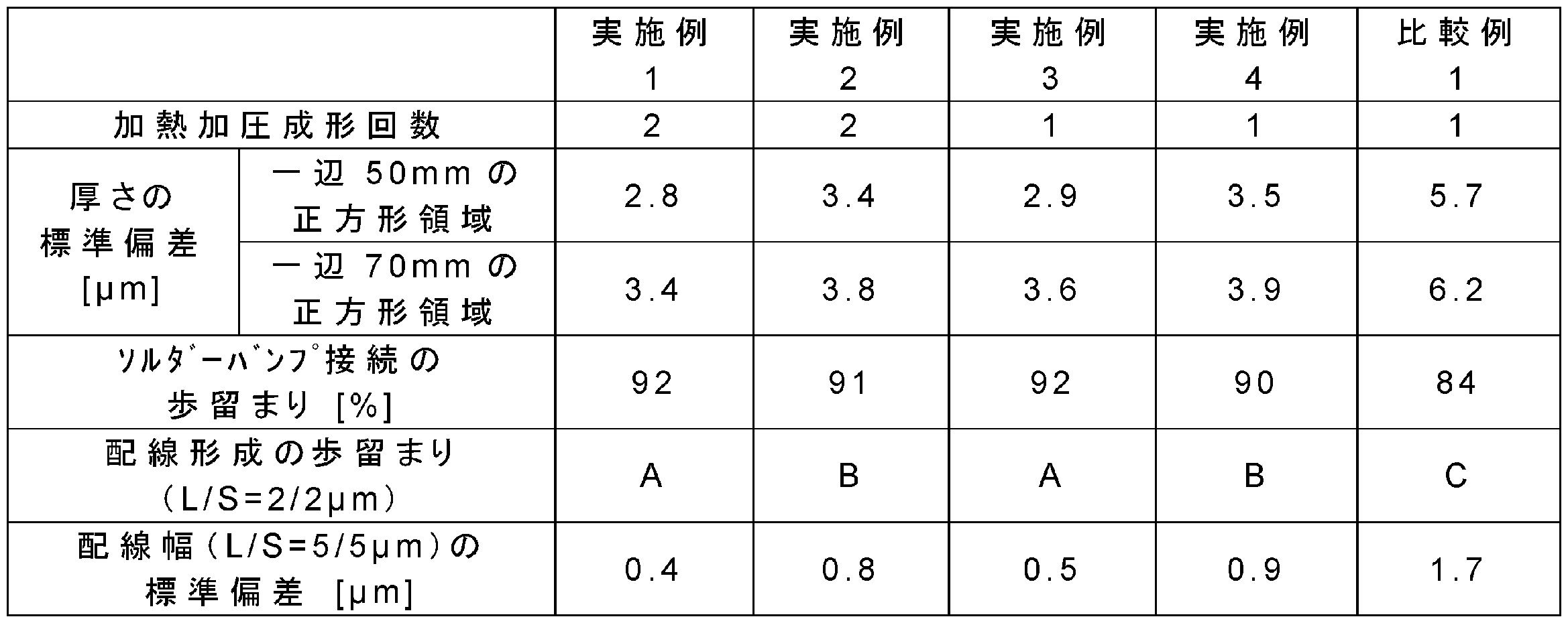
上記方法によって得られた有機コア材について、下記評価方法に従って各評価を行った。結果を表1に示す。
<50mm角サイズの厚さ標準偏差の算出>
250mm角サイズ(平面視で一辺250mmの正方形)の有機コア材の中心の150mm角サイズの範囲を、50mm角の9個のエリアに分け、9エリアの厚さの標準偏差の値を算出した。サーバ向けの大型のパッケージの場合、チップサイズが50mm角程度になることを想定し、50mm角を標準偏差算出の範囲に設定した。中心の150mm角サイズより外側は、プリプレグに含まれる樹脂がプリプレグの外側に流出し有機コア材が薄くなるため、評価には使用しなかった。
250mm角サイズ(平面視で一辺250mmの正方形)の有機コア材の中心の150mm角サイズの範囲を、50mm角の9個のエリアに分け、9エリアの厚さの標準偏差の値を算出した。サーバ向けの大型のパッケージの場合、チップサイズが50mm角程度になることを想定し、50mm角を標準偏差算出の範囲に設定した。中心の150mm角サイズより外側は、プリプレグに含まれる樹脂がプリプレグの外側に流出し有機コア材が薄くなるため、評価には使用しなかった。
マイクロメータ(株式会社ミツトヨ製、ID-C112X)を用いて、50mm角のエリアの四隅の4点の厚さを測定した。4点の厚さの値を母集団として標準偏差の値を算出した。9エリアから算出した標準偏差の値のうち最大の値を、各有機コア材の標準偏差の値として表1に記載した。
<70mm角サイズの厚さ標準偏差の算出>
250mm角サイズ(平面視で一辺250mmの正方形)の有機コア材の中心の140mm角サイズの範囲を、70mm角の4個のエリアに分け、4エリアの厚さの標準偏差の値を算出した。銅配線形成工程における、フォトレジストパターン形成時のUVの照射範囲が70mm角であることから、70mm角を標準偏差算出の範囲に設定した。マイクロメータを用いて、70mm角のエリアの4隅の4点の厚さを測定した。4点の厚さの値を母集団として標準偏差の値を算出した。4エリアから算出した標準偏差の値のうち最大の値を、各有機コア材の標準偏差の値として表1に記載した。
250mm角サイズ(平面視で一辺250mmの正方形)の有機コア材の中心の140mm角サイズの範囲を、70mm角の4個のエリアに分け、4エリアの厚さの標準偏差の値を算出した。銅配線形成工程における、フォトレジストパターン形成時のUVの照射範囲が70mm角であることから、70mm角を標準偏差算出の範囲に設定した。マイクロメータを用いて、70mm角のエリアの4隅の4点の厚さを測定した。4点の厚さの値を母集団として標準偏差の値を算出した。4エリアから算出した標準偏差の値のうち最大の値を、各有機コア材の標準偏差の値として表1に記載した。
<ソルダーバンプ接続の歩留まりの評価>
250mm角サイズ(平面視で一辺250mmの正方形)の有機コア材を準備した。この有機コア材の中心領域(150mm角サイズの範囲)を裁断機で30mm角サイズに裁断した。裁断には、リファイン・ソー・エクセルA(リファインテック株式会社製)を使用した。裁断後、10質量%硫酸水溶液に1分間浸漬して基板表面を洗浄した。その後、純水を用いて洗浄した。
250mm角サイズ(平面視で一辺250mmの正方形)の有機コア材を準備した。この有機コア材の中心領域(150mm角サイズの範囲)を裁断機で30mm角サイズに裁断した。裁断には、リファイン・ソー・エクセルA(リファインテック株式会社製)を使用した。裁断後、10質量%硫酸水溶液に1分間浸漬して基板表面を洗浄した。その後、純水を用いて洗浄した。
フラックス(千住金属工業製、SPARKLE FLUX WF-6317)を基板表面に塗布した後、以下に説明するソルダーバンプ付きチップ(ウォルツ製、FBW150-0001JY)を乗せた。その後、260℃の窒素リフロー炉(千住金属工業製、SNR-1065GT)に入れチップを基板に実装した。
ソルダーバンプ付きチップは、シリコンウェハ表面に銅のピラーが配置され、銅のピラーのシリコンウェハと異なる端面にソルダーが配置された構造を有する。銅のピラーとソルダーを合わせてソルダーバンプと称される。各構成のサイズは以下のとおりであった。
・ソルダーバンプ付きチップの大きさ:25mm角
・シリコンウェハの厚さ:725±25μm
・ソルダーバンプのピッチ:150μm
・銅のピラーの高さ:45μm
・ソルダーバンプの高さ:15μm
・ソルダーの直径:75μm
・ソルダーバンプ付きチップの大きさ:25mm角
・シリコンウェハの厚さ:725±25μm
・ソルダーバンプのピッチ:150μm
・銅のピラーの高さ:45μm
・ソルダーバンプの高さ:15μm
・ソルダーの直径:75μm
超音波洗浄機(アズワン製、VS-100III)を用いて、ソルダーバンプ付きチップと有機コア材の間のフラックスを除去した。条件は、周波数45kHz, 洗浄時間10分間とした。その後、オーブン(ヤマト科学製、DKN402)に入れ、100℃で30分間加熱して乾燥した。110℃に加熱したホットプレートにソルダーバンプ付きチップを実装した有機コア材を乗せ、有機コア材とソルダーバンプ付きチップの間にCUF(Capillary Underfill、日立化成株式会社製、CEL-C-3730S)を注入した。その後、オーブンに入れ150℃で2時間加熱して硬化した。
ソルダーバンプ付きチップを実装した有機コア材をエポキシ樹脂で注型した後、有機コア材とソルダーバンプ付きチップの断面を観察し、ソルダーバンプと有機コア材表面の銅箔が接続している箇所を数えた。接続を確認する箇所は、ソルダーバンプ付きチップの四隅のソルダーバンプそれぞれ10箇所、計40箇所とした。各試料の試験体数は3とし、合わせて120箇所のソルダーバンプに対して、銅箔と接続しているかどうかを調べた。ソルダーバンプ120箇所のうち、接続しているソルダーバンプの割合を算出し、これをソルダーバンプ接続歩留まりとした。
<配線形成の歩留まりの評価>
セミアディティブ法により、有機コア材に銅配線を形成した。まず、有機コア材の銅箔を過硫酸アンモニウム水溶液に浸漬してエッチングした。その後、有機コア材の両面に熱硬化性樹脂絶縁体のビルドアップフィルム(味の素ファインテクノ株式会社製、GX92)をラミネートした。真空ラミネータ(ニッコー・マテリアルズ株式会社製、V-130)を使用した。条件は圧力0.5MPa、真空引き時間15秒間、加圧時間60秒間、温度50℃とした。その後、オーブンに入れ130℃で15分間加熱して乾燥し、190℃で120分間加熱して硬化した。これにより、有機コア材の両面に絶縁層15をそれぞれ形成した(図5(a))。
セミアディティブ法により、有機コア材に銅配線を形成した。まず、有機コア材の銅箔を過硫酸アンモニウム水溶液に浸漬してエッチングした。その後、有機コア材の両面に熱硬化性樹脂絶縁体のビルドアップフィルム(味の素ファインテクノ株式会社製、GX92)をラミネートした。真空ラミネータ(ニッコー・マテリアルズ株式会社製、V-130)を使用した。条件は圧力0.5MPa、真空引き時間15秒間、加圧時間60秒間、温度50℃とした。その後、オーブンに入れ130℃で15分間加熱して乾燥し、190℃で120分間加熱して硬化した。これにより、有機コア材の両面に絶縁層15をそれぞれ形成した(図5(a))。
一方のビルドアップフィルム層の表面に、スパッタリング法によってシード層16を形成した(図5(b))。シード層16は、チタン層25nmと銅層150nmとの二層構造とした。その後、真空ラミネータを用いて、感光性樹脂組成物のフォトレジストフィルム(日立化成株式会社製、RY-5107UT)をシード層上にラミネートした。条件は圧力0.5MPa、真空引き時間15秒間、加圧時間60秒間、温度50℃とした。これにより、シード層16の表面に感光性樹脂層17を形成した(図5(c))。
投影露光装置(株式会社サーマプレシジョン製、S6Ck露光機)を用いて一辺70mmの正方形の領域にUVを照射して露光した。その後、スピン現像機(ブルーオーシャンテクノロジー株式会社製、超高圧スピン現像装置)を用いて炭酸ナトリウム1質量%水溶液をスプレーして現像した。この工程によってレジスト幅/スペース幅=2μm/2μmのパターンを作製した(図6(a))。その後、プラズマアッシャー(ノードソン・アドバンスト・テクノロジー株式会社製、APシリーズ バッチ式プラズマ処理装置)を用いて、酸素プラズマをレジストパターンに当てることで、現像時のレジスト残渣を取り除いた。
電解銅めっき法により、配線幅/スペース幅(L/S)=2μm/2μmの銅配線18を形成した(図6(b))。配線高さは3μmとした。スピン現像機でTMAH(水酸化テトラメチルアンモニウム)2.38質量%水溶液をスプレーし、レジストを剥離した(図6(c))。レジストの剥離によって露出したシード層16をエッチングによって除去した(図7)。銅層は銅のエッチング液(三菱ガス化学製、WLC-C2)と純水を1:1の質量比で混合した水溶液に23℃で45秒間浸漬後、純水洗浄して除去した。チタン層はチタンのエッチング液(三菱ガス化学製、WLC-T)と23%のアンモニア水溶液を50:1の質量比で混合した水溶液に23℃で65秒間浸漬後、純水洗浄して除去した。
金属顕微鏡で、配線幅/スペース幅=2μm/2μmの銅配線を観察し、配線倒れ、配線の欠損、配線同士の繋がり、配線の変形等の不良が無い配線の数を計測し、作製した45か所の配線に対する割合を算出した。これを配線歩留まりとした。評価基準は以下のとおりとした。
A:配線歩留まりが75%以上100%以下
B:配線歩留まりが50%以上75%未満
C:配線歩留まりが0%以上50%未満
A:配線歩留まりが75%以上100%以下
B:配線歩留まりが50%以上75%未満
C:配線歩留まりが0%以上50%未満
<配線幅の測定>
セミアディティブ法で作製した銅配線(銅配線:設計値の配線幅/スペース幅(L/S)=5μm/5μm)の断面をSU8200形走査電子顕微鏡(株式会社日立ハイテクノロジーズ、)を用いて観察し、配線の幅を測定した。一度にUV照射ができる範囲(一辺70mmの正方形)の中心と、この正方形の四つの頂点のうちの一つの頂点と、この頂点と対角に位置する頂点とに対応する計三つの測定点において配線幅を測定した。三つの測定値を母集団として標準偏差を算出した。
セミアディティブ法で作製した銅配線(銅配線:設計値の配線幅/スペース幅(L/S)=5μm/5μm)の断面をSU8200形走査電子顕微鏡(株式会社日立ハイテクノロジーズ、)を用いて観察し、配線の幅を測定した。一度にUV照射ができる範囲(一辺70mmの正方形)の中心と、この正方形の四つの頂点のうちの一つの頂点と、この頂点と対角に位置する頂点とに対応する計三つの測定点において配線幅を測定した。三つの測定値を母集団として標準偏差を算出した。
本開示によれば、半導体パッケージの高密度化及び高い信頼性をより一層高度に実現するのに有用な有機コア材及びその製造方法が提供される。
1…第一の層、1a…第一の繊維クロス、1b…第一の樹脂層(硬化前)、1B…第一の樹脂層(硬化後)、2…第二の層、2a…第二の繊維クロス、2b…第二の樹脂層(硬化前)、2B…第二の樹脂層(硬化後)、3…樹脂層、5…金属箔、10…有機コア材、20…積層体、10P,20P,30P…積層体、15…絶縁層、16…シード層、17…感光性樹脂層、18…銅配線、F1,F2…表面、P1…第一のプリプレグ、P2…第二のプリプレグ。
Claims (7)
- 第一の繊維クロスと、第一の樹脂成分からなり且つ前記第一の繊維クロスが埋め込まれている第一の樹脂層とをそれぞれ有する複数の第一のプリプレグを準備する工程と、
第二の繊維クロスと、第二の樹脂成分からなり且つ前記第二の繊維クロスが埋め込まれている第二の樹脂層とをそれぞれ有する少なくとも二枚の第二のプリプレグを準備する工程と、
前記第二のプリプレグと、複数の前記第一のプリプレグと、前記第二のプリプレグとをこの順序で備える積層体の厚さ方向に押圧力を加えながら加熱する工程と、
を含み、
前記第二のプリプレグの質量を基準とする前記第二の樹脂成分の含有率が前記第一のプリプレグの質量を基準とする前記第一の樹脂成分の含有率よりも高い、有機コア材の製造方法。 - 第一の繊維クロスと、第一の樹脂成分からなり且つ前記第一の繊維クロスが埋め込まれている第一の樹脂層とをそれぞれ有する複数の第一のプリプレグを準備する工程と、
第二の繊維クロスと、第二の樹脂成分からなり且つ前記第二の繊維クロスが埋め込まれている第二の樹脂層とをそれぞれ有する少なくとも二枚の第二のプリプレグを準備する工程と、
複数の前記第一のプリプレグの第一の積層体の厚さ方向に押圧力を加えながら加熱する工程と、
前記第二のプリプレグと、前記第一の積層体と、前記第二のプリプレグとをこの順序で備える第二の積層体の厚さ方向に押圧力を加えながら加熱する工程と、
を含み、
前記第二のプリプレグの質量を基準とする前記第二の樹脂成分の含有率が前記第一のプリプレグの質量を基準とする前記第一の樹脂成分の含有率よりも高い、有機コア材の製造方法。 - 前記第二のプリプレグの質量を基準とする前記第二の樹脂成分の含有率が60質量%以上である、請求項1又は2に記載の有機コア材の製造方法。
- 平面視において一辺50mmの正方形の頂点に相当する4点における厚さの標準偏差が3.5μm以下である、有機コア材。
- 第一の繊維クロスと、第一の樹脂成分からなり且つ前記第一の繊維クロスが埋め込まれている第一の樹脂層とを有する第一の層と、
第二の繊維クロスと、第二の樹脂成分からなり且つ前記第二の繊維クロスが埋め込まれている第二の樹脂層とを有する第二の層と、
を備え、
前記第二の層と、複数の前記第一の層と、前記第二の層とをこの順序で備える積層構造を有し、
前記第二の樹脂層の質量を基準とする前記第二の樹脂成分の含有率が前記第一の樹脂層の質量を基準とする前記第一の樹脂成分の含有率よりも高い、有機コア材。 - 複数の層を有する有機コア材であって、
当該有機コア材の縦断面において繊維クロスと樹脂層が交互に配置されており、
平面視において一辺50mmの正方形の頂点に相当する4点における厚さの標準偏差が3.5μm以下である、有機コア材。 - 当該有機コア材の縦断面において、当該有機コア材の表面近傍に、当該有機コア材の中央部に配置された前記繊維クロスよりも薄い前記繊維クロスが配置されている、請求項6に記載の有機コア材。
Priority Applications (6)
| Application Number | Priority Date | Filing Date | Title |
|---|---|---|---|
| PCT/JP2020/035461 WO2022059166A1 (ja) | 2020-09-18 | 2020-09-18 | 有機コア材及びその製造方法 |
| JP2022550588A JP7746998B2 (ja) | 2020-09-18 | 2021-09-15 | 有機コア材及びその製造方法、有機コア材を含む積層体、並びに配線板 |
| KR1020237011220A KR20230069944A (ko) | 2020-09-18 | 2021-09-15 | 유기 코어재 및 그 제조 방법, 유기 코어재를 포함하는 적층체, 및 배선판 |
| PCT/JP2021/033953 WO2022059711A1 (ja) | 2020-09-18 | 2021-09-15 | 有機コア材及びその製造方法、有機コア材を含む積層体、並びに配線板 |
| US18/245,348 US20230356498A1 (en) | 2020-09-18 | 2021-09-15 | Organic core material, production method for same, laminate including organic core material, and circuit board |
| TW110134532A TWI910228B (zh) | 2020-09-18 | 2021-09-16 | 有機芯材及其製造方法、包含有機芯材之積層體、以及配線板 |
Applications Claiming Priority (1)
| Application Number | Priority Date | Filing Date | Title |
|---|---|---|---|
| PCT/JP2020/035461 WO2022059166A1 (ja) | 2020-09-18 | 2020-09-18 | 有機コア材及びその製造方法 |
Publications (1)
| Publication Number | Publication Date |
|---|---|
| WO2022059166A1 true WO2022059166A1 (ja) | 2022-03-24 |
Family
ID=80776032
Family Applications (2)
| Application Number | Title | Priority Date | Filing Date |
|---|---|---|---|
| PCT/JP2020/035461 Ceased WO2022059166A1 (ja) | 2020-09-18 | 2020-09-18 | 有機コア材及びその製造方法 |
| PCT/JP2021/033953 Ceased WO2022059711A1 (ja) | 2020-09-18 | 2021-09-15 | 有機コア材及びその製造方法、有機コア材を含む積層体、並びに配線板 |
Family Applications After (1)
| Application Number | Title | Priority Date | Filing Date |
|---|---|---|---|
| PCT/JP2021/033953 Ceased WO2022059711A1 (ja) | 2020-09-18 | 2021-09-15 | 有機コア材及びその製造方法、有機コア材を含む積層体、並びに配線板 |
Country Status (5)
| Country | Link |
|---|---|
| US (1) | US20230356498A1 (ja) |
| JP (1) | JP7746998B2 (ja) |
| KR (1) | KR20230069944A (ja) |
| TW (1) | TWI910228B (ja) |
| WO (2) | WO2022059166A1 (ja) |
Families Citing this family (3)
| Publication number | Priority date | Publication date | Assignee | Title |
|---|---|---|---|---|
| US20230143137A1 (en) * | 2020-04-21 | 2023-05-11 | Kyocera Corporation | Electronic component, electronic device, and method for manufacturing electronic component |
| JP7635894B2 (ja) * | 2022-12-07 | 2025-02-26 | 株式会社レゾナック | 金属張り積層板、プリント配線板及び半導体パッケージ |
| JPWO2024122586A1 (ja) * | 2022-12-07 | 2024-06-13 |
Citations (2)
| Publication number | Priority date | Publication date | Assignee | Title |
|---|---|---|---|---|
| JPH0697670A (ja) * | 1992-02-26 | 1994-04-08 | Risho Kogyo Co Ltd | 多層プリント配線用基板 |
| JP2007110044A (ja) * | 2005-10-17 | 2007-04-26 | Kyocera Chemical Corp | 銅張り積層板 |
Family Cites Families (6)
| Publication number | Priority date | Publication date | Assignee | Title |
|---|---|---|---|---|
| JPH02155726A (ja) * | 1988-12-09 | 1990-06-14 | Sumitomo Bakelite Co Ltd | 熱硬化性樹脂積層板の製造方法 |
| JPH05261861A (ja) * | 1992-03-19 | 1993-10-12 | Shin Kobe Electric Mach Co Ltd | 積層板 |
| JP2985642B2 (ja) * | 1994-02-23 | 1999-12-06 | 松下電工株式会社 | 金属張り積層板の製造方法 |
| KR101763975B1 (ko) | 2010-05-07 | 2017-08-01 | 스미토모 베이클리트 컴퍼니 리미티드 | 회로 기판용 에폭시 수지 조성물, 프리프레그, 적층판, 수지 시트, 프린트 배선판용 적층기재, 프린트 배선판, 및 반도체 장치 |
| JP2014167053A (ja) * | 2013-02-28 | 2014-09-11 | 3M Innovative Properties Co | 高熱伝導性プリプレグ、プリプレグを用いた配線板および多層配線板、ならびに多層配線板を用いた半導体装置 |
| JP6133227B2 (ja) | 2014-03-27 | 2017-05-24 | 新光電気工業株式会社 | 配線基板及びその製造方法 |
-
2020
- 2020-09-18 WO PCT/JP2020/035461 patent/WO2022059166A1/ja not_active Ceased
-
2021
- 2021-09-15 WO PCT/JP2021/033953 patent/WO2022059711A1/ja not_active Ceased
- 2021-09-15 US US18/245,348 patent/US20230356498A1/en active Pending
- 2021-09-15 JP JP2022550588A patent/JP7746998B2/ja active Active
- 2021-09-15 KR KR1020237011220A patent/KR20230069944A/ko active Pending
- 2021-09-16 TW TW110134532A patent/TWI910228B/zh active
Patent Citations (2)
| Publication number | Priority date | Publication date | Assignee | Title |
|---|---|---|---|---|
| JPH0697670A (ja) * | 1992-02-26 | 1994-04-08 | Risho Kogyo Co Ltd | 多層プリント配線用基板 |
| JP2007110044A (ja) * | 2005-10-17 | 2007-04-26 | Kyocera Chemical Corp | 銅張り積層板 |
Also Published As
| Publication number | Publication date |
|---|---|
| JP7746998B2 (ja) | 2025-10-01 |
| KR20230069944A (ko) | 2023-05-19 |
| WO2022059711A1 (ja) | 2022-03-24 |
| TWI910228B (zh) | 2026-01-01 |
| JPWO2022059711A1 (ja) | 2022-03-24 |
| US20230356498A1 (en) | 2023-11-09 |
| TW202212151A (zh) | 2022-04-01 |
Similar Documents
| Publication | Publication Date | Title |
|---|---|---|
| JP7746998B2 (ja) | 有機コア材及びその製造方法、有機コア材を含む積層体、並びに配線板 | |
| JP5569270B2 (ja) | プリプレグ、金属張積層板、プリント配線板及び半導体装置 | |
| TWI433773B (zh) | 積層板,電路板及半導體裝置 | |
| JP6206035B2 (ja) | 金属張積層板、プリント配線基板、および半導体装置 | |
| WO2022059716A1 (ja) | 半導体パッケージ用基板材料を製造する方法、プリプレグ、及び半導体パッケージ用基板材料 | |
| TW201811556A (zh) | 覆金屬積層板、印刷線路板及半導體封裝體 | |
| JP7351315B2 (ja) | 金属張り積層板の製造方法、金属張り積層板、プリント配線板及び半導体パッケージ、並びにコアレス基板形成用支持体及び半導体再配線層形成用支持体 | |
| TW202033361A (zh) | 積層板、印刷線路板、半導體封裝體及積層板的製造方法 | |
| JP5594128B2 (ja) | プリント配線板用樹脂組成物、プリプレグ、積層板、樹脂シート、プリント配線板及び半導体装置 | |
| KR20240053065A (ko) | 반도체 패키지용 기판 재료를 제조하는 방법, 프리프레그, 및 프리프레그의 응용 | |
| JP5256681B2 (ja) | 半導体装置、半導体装置用プリント配線板及び銅張積層板 | |
| TW202417553A (zh) | 預浸體、積層板、印刷線路板及半導體封裝體 | |
| JP5293654B2 (ja) | 回路基板用樹脂組成物、プリプレグ、積層板、プリント配線板、及び半導体装置 | |
| JP2022164680A (ja) | プリプレグ及びその製造方法、積層板、プリント配線板並びに半導体パッケージ | |
| JP7529188B1 (ja) | 金属張積層板、プリント配線板及び半導体パッケージ並びにこれらの製造方法 | |
| JP2012158645A (ja) | プリント配線板用エポキシ樹脂組成物、プリプレグ、金属張積層板、樹脂シート、プリント配線板及び半導体装置 | |
| WO2025173767A1 (ja) | 半導体パッケージ | |
| WO2025258595A1 (ja) | 金属張積層板の製造方法、金属張積層板、プリント配線板及びその製造方法、半導体パッケージ及びその製造方法 | |
| JP5211624B2 (ja) | 半導体装置の製造方法および半導体装置用プリント配線板の製造方法 | |
| TW202212119A (zh) | 積層板、印刷線路板、半導體封裝體及積層板的製造方法 | |
| TW202436096A (zh) | 覆金屬積層板、印刷線路板及半導體封裝體 |
Legal Events
| Date | Code | Title | Description |
|---|---|---|---|
| 121 | Ep: the epo has been informed by wipo that ep was designated in this application |
Ref document number: 20954151 Country of ref document: EP Kind code of ref document: A1 |
|
| NENP | Non-entry into the national phase |
Ref country code: DE |
|
| 122 | Ep: pct application non-entry in european phase |
Ref document number: 20954151 Country of ref document: EP Kind code of ref document: A1 |
|
| NENP | Non-entry into the national phase |
Ref country code: JP |