WO2022054729A1 - コンデンサ - Google Patents
コンデンサ Download PDFInfo
- Publication number
- WO2022054729A1 WO2022054729A1 PCT/JP2021/032548 JP2021032548W WO2022054729A1 WO 2022054729 A1 WO2022054729 A1 WO 2022054729A1 JP 2021032548 W JP2021032548 W JP 2021032548W WO 2022054729 A1 WO2022054729 A1 WO 2022054729A1
- Authority
- WO
- WIPO (PCT)
- Prior art keywords
- connection terminal
- bus bar
- terminal portion
- recess
- protrusion
- Prior art date
Links
- 239000003990 capacitor Substances 0.000 title claims abstract description 105
- 229920005989 resin Polymers 0.000 claims description 35
- 239000011347 resin Substances 0.000 claims description 35
- 238000005452 bending Methods 0.000 claims description 12
- 239000010408 film Substances 0.000 description 31
- 238000012986 modification Methods 0.000 description 20
- 230000004048 modification Effects 0.000 description 20
- 238000005304 joining Methods 0.000 description 13
- 238000000034 method Methods 0.000 description 12
- 238000005476 soldering Methods 0.000 description 11
- 229910052751 metal Inorganic materials 0.000 description 10
- 239000002184 metal Substances 0.000 description 10
- 239000011104 metalized film Substances 0.000 description 8
- 238000003466 welding Methods 0.000 description 8
- 238000012544 monitoring process Methods 0.000 description 5
- 229910052782 aluminium Inorganic materials 0.000 description 4
- XAGFODPZIPBFFR-UHFFFAOYSA-N aluminium Chemical compound [Al] XAGFODPZIPBFFR-UHFFFAOYSA-N 0.000 description 4
- 238000010030 laminating Methods 0.000 description 4
- 150000002739 metals Chemical class 0.000 description 4
- 238000000465 moulding Methods 0.000 description 4
- RYGMFSIKBFXOCR-UHFFFAOYSA-N Copper Chemical compound [Cu] RYGMFSIKBFXOCR-UHFFFAOYSA-N 0.000 description 3
- 239000004020 conductor Substances 0.000 description 3
- 229910052802 copper Inorganic materials 0.000 description 3
- 239000010949 copper Substances 0.000 description 3
- 230000000694 effects Effects 0.000 description 3
- 239000007791 liquid phase Substances 0.000 description 3
- 238000004804 winding Methods 0.000 description 3
- 239000004734 Polyphenylene sulfide Substances 0.000 description 2
- HCHKCACWOHOZIP-UHFFFAOYSA-N Zinc Chemical compound [Zn] HCHKCACWOHOZIP-UHFFFAOYSA-N 0.000 description 2
- 230000015572 biosynthetic process Effects 0.000 description 2
- 238000000151 deposition Methods 0.000 description 2
- 238000009434 installation Methods 0.000 description 2
- 229920000069 polyphenylene sulfide Polymers 0.000 description 2
- 229910052725 zinc Inorganic materials 0.000 description 2
- 239000011701 zinc Substances 0.000 description 2
- FYYHWMGAXLPEAU-UHFFFAOYSA-N Magnesium Chemical compound [Mg] FYYHWMGAXLPEAU-UHFFFAOYSA-N 0.000 description 1
- 239000000956 alloy Substances 0.000 description 1
- 229910045601 alloy Inorganic materials 0.000 description 1
- 239000000470 constituent Substances 0.000 description 1
- 239000003822 epoxy resin Substances 0.000 description 1
- 229910052749 magnesium Inorganic materials 0.000 description 1
- 239000011777 magnesium Substances 0.000 description 1
- 238000004519 manufacturing process Methods 0.000 description 1
- 238000001465 metallisation Methods 0.000 description 1
- 238000012806 monitoring device Methods 0.000 description 1
- 230000000149 penetrating effect Effects 0.000 description 1
- 239000012071 phase Substances 0.000 description 1
- 229920000647 polyepoxide Polymers 0.000 description 1
- 238000003825 pressing Methods 0.000 description 1
- 239000004065 semiconductor Substances 0.000 description 1
- 238000005507 spraying Methods 0.000 description 1
- 229920005992 thermoplastic resin Polymers 0.000 description 1
- 229920001187 thermosetting polymer Polymers 0.000 description 1
Images


Classifications
-
- H—ELECTRICITY
- H01—ELECTRIC ELEMENTS
- H01G—CAPACITORS; CAPACITORS, RECTIFIERS, DETECTORS, SWITCHING DEVICES, LIGHT-SENSITIVE OR TEMPERATURE-SENSITIVE DEVICES OF THE ELECTROLYTIC TYPE
- H01G2/00—Details of capacitors not covered by a single one of groups H01G4/00-H01G11/00
- H01G2/10—Housing; Encapsulation
-
- H—ELECTRICITY
- H01—ELECTRIC ELEMENTS
- H01G—CAPACITORS; CAPACITORS, RECTIFIERS, DETECTORS, SWITCHING DEVICES, LIGHT-SENSITIVE OR TEMPERATURE-SENSITIVE DEVICES OF THE ELECTROLYTIC TYPE
- H01G4/00—Fixed capacitors; Processes of their manufacture
- H01G4/002—Details
- H01G4/224—Housing; Encapsulation
-
- H—ELECTRICITY
- H01—ELECTRIC ELEMENTS
- H01G—CAPACITORS; CAPACITORS, RECTIFIERS, DETECTORS, SWITCHING DEVICES, LIGHT-SENSITIVE OR TEMPERATURE-SENSITIVE DEVICES OF THE ELECTROLYTIC TYPE
- H01G4/00—Fixed capacitors; Processes of their manufacture
- H01G4/002—Details
- H01G4/228—Terminals
-
- H—ELECTRICITY
- H01—ELECTRIC ELEMENTS
- H01G—CAPACITORS; CAPACITORS, RECTIFIERS, DETECTORS, SWITCHING DEVICES, LIGHT-SENSITIVE OR TEMPERATURE-SENSITIVE DEVICES OF THE ELECTROLYTIC TYPE
- H01G4/00—Fixed capacitors; Processes of their manufacture
- H01G4/32—Wound capacitors
Definitions
- the present invention relates to a capacitor.
- a protrusion is provided on the case, and a fitting hole for fitting the protrusion of the case is provided on the bus bar connected to the electrode of the capacitor element. Then, the bus bar is positioned and fixed to the case by fitting the protrusion and the fitting hole.
- an object of the present invention is to provide a capacitor that can easily install a bus bar on a case.
- the main aspect of the present invention relates to a capacitor.
- the capacitor according to this embodiment includes a capacitor element, an electrode terminal portion and a connection terminal portion, and has a bus bar in which the electrode terminal portion is connected to the electrode of the capacitor element and a case having an accommodating portion for accommodating the capacitor element. , Equipped with.
- the connection terminal portion is positioned outside the accommodating portion and has a protrusion, and the case has a recess into which the protrusion is inserted.
- the bus bar can be easily installed on the case.
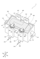
- FIG. 1 is a perspective view of a film capacitor according to an embodiment.
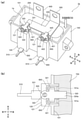
- FIG. 2 is an exploded perspective view of a capacitor element unit composed of a capacitor element, a first bus bar, and a second bus bar according to an embodiment.
- FIG. 3 is an exploded perspective view of a structure composed of a capacitor element unit, a case, a first terminal, and a second terminal according to an embodiment.
- FIG. 4A is a perspective view of a structure including a capacitor element unit, a case, a first terminal, and a second terminal according to an embodiment.
- FIG. 4B is a top view of the vicinity of the box-shaped portion on the left side in a state where the structure is filled with the filling resin according to the embodiment.
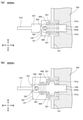
- FIG. 5 (a) and 5 (b) are cross-sectional views in the vicinity of the two recesses formed on the upper surface of the box-shaped portion on the left side, respectively, according to the embodiment.
- 6 (a) and 6 (b) are cross-sectional views in the vicinity of the two recesses formed on the upper surface of the box-shaped portion on the left side, respectively, according to the first modification.
- FIG. 7A is a top view of the vicinity of the box-shaped portion on the left side according to the second modification.
- FIG. 7B is a top view of the vicinity of the box-shaped portion on the left side according to the modified example 3.
- the film capacitor 1 which is an embodiment of the capacitor of the present invention, will be described with reference to the drawings.
- each figure is appropriately marked with front-back, left-right, and up-down directions.
- a plane parallel to the front-back and left-right directions is referred to as a horizontal plane for convenience.
- the direction shown in the figure merely indicates the relative direction of the film capacitor 1, and does not indicate the absolute direction.
- the film capacitor 1 corresponds to the "capacitor” described in the claims.
- the notch 101a corresponds to the "connection passage” described in the claims.
- the first electrode 210 and the second electrode 220 correspond to the “electrode” described in the claims.
- the first bus bar 300 and the second bus bar 400 correspond to the "bus bar” described in the claims.
- the first terminal 500 and the second terminal 600 correspond to the "terminals” described in the claims.
- the external connection terminal portions 510 and 610 correspond to the "one end” described in the claims.
- the connection terminal portions 520 and 620 correspond to the “other end” described in the claims.
- the filling resin 700 corresponds to the "resin” described in the claims.
- FIG. 1 is a perspective view of the film capacitor 1.
- the outline configuration of the film capacitor 1 will be described with reference to FIG. 1, and the detailed configuration of each part will be described later with reference to FIGS. 2 and later.
- the film capacitor 1 includes a case 100, a capacitor element 200, a first bus bar 300, a second bus bar 400, a first terminal 500, a second terminal 600, and a filling resin 700.
- the case 100 is formed in a substantially rectangular parallelepiped box shape, and has a housing portion 101 having an open upper portion inside.
- the accommodating portion 101 accommodates the capacitor element 200.
- Mounting tabs 110 are provided on the left and right outer surfaces of the case 100, respectively.
- a hole 111 penetrating in the front-rear direction is formed in the mounting tab 110, and a metal collar 112 for increasing the strength of the hole is fitted in the hole 111.
- a mounting tab is provided on the outer bottom surface of the case 100 as well as the outer surface, and a metal collar is fitted into the hole of the mounting tab.
- two box-shaped portions 120 are provided side by side with an interval in the left-right direction.
- the first terminal 500 and the second terminal 600 are installed on the left side and the right side box-shaped portions 120 by insert molding, respectively.
- the terminals of the external device are connected to the external connection terminal portion 510 of the first terminal 500 and the external connection terminal portion 610 of the second terminal 600, respectively.
- two recesses 800 extending in the front-rear direction are provided side by side with an interval in the left-right direction.
- the first bus bar 300 and the second bus bar 400 are installed on the upper surface and the lower surface of the capacitor element 200, respectively.
- the external connection terminal portion 310 of the first bus bar 300 and the external connection terminal portion 410 of the second bus bar 400 each extend upward and are positioned outside the accommodating portion 101.
- the terminals of the external device are connected to the external connection terminal portions 310 and 410, respectively.
- connection terminal portion 320 of the first bus bar 300 and the connection terminal portion 420 of the second bus bar 400 are located outside the accommodating portion 101, and the connection terminal portion 520 and the second terminal 600 at the upper end of the first terminal 500, respectively. It is connected to the connection terminal portion 620 at the upper end of the bus by a joining method such as soldering.
- the filling resin 700 is a thermosetting resin such as an epoxy resin, and the capacitor element 200 is injected into the housing section 101 in a liquid phase state while being housed in the housing section 101 of the case 100, and then the case 100 is injected. It cures when heated. The portions of the first bus bar 300 and the second bus bar 400 in the accommodating portion 101 and the capacitor element 200 are protected from moisture and impact by the filling resin 700.
- FIG. 2 is an exploded perspective view of a capacitor element unit 1a composed of a capacitor element 200, a first bus bar 300, and a second bus bar 400.
- the first bus bar 300 is composed of an external connection terminal portion 310, a connection terminal portion 320, and an electrode terminal portion 330.
- the first bus bar 300 is formed by appropriately bending or otherwise processing a metal plate (for example, a copper plate) which is a conductive material having a predetermined shape.
- the electrode terminal portion 330 has a flat plate shape parallel to a horizontal plane.
- the external connection terminal portion 310 has a flat plate shape and extends upward from the rear end of the electrode terminal portion 330.
- the external connection terminal portion 310 is formed with a mounting hole 311 that penetrates the external connection terminal portion 310 in the front-rear direction. After the assembly of the film capacitor 1 is completed, the terminal of the external device is connected to the external connection terminal portion 310 by screwing using the mounting hole 311.
- a flat plate-shaped connecting portion 331 extending upward is formed in the vicinity of the left end of the front end of the electrode terminal portion 330.
- the width of the connection portion 331 in the left-right direction is narrower than the width of the external connection terminal portion 310 in the left-right direction.
- the connection terminal portion 320 has a flat plate shape parallel to the horizontal plane and extends forward from the upper end of the connection portion 331.
- the connection terminal portion 320 has a main body portion 320a having a width equal to that of the connection portion 331 in the left-right direction.
- a flange portion 320b extending slightly outward in the left-right direction is formed at the left end and the right end of the main body portion 320a, and a flat plate-shaped protrusion 321 extending downward is formed at the outer end portion of the flange portion 320b.
- the left and right protrusions 321 are formed symmetrically with respect to the center of the main body 320a.
- the protrusion 321 is formed by bending a part of the connection terminal portion 320 parallel to the horizontal plane downward.
- the left and right side surfaces of the protrusion 321 have a rectangular shape.
- connection hole 322 that penetrates the connection terminal portion 320 in the vertical direction is formed in the vicinity of the front end of the connection terminal portion 320.
- the connection terminal portion 520 (see FIG. 3) at the upper end of the first terminal 500 is connected to the connection hole 322 by a joining method such as soldering.
- the second bus bar 400 has substantially the same configuration as the first bus bar 300, and is composed of an external connection terminal portion 410, a connection terminal portion 420, and an electrode terminal portion 430.
- the second bus bar 400 is formed by appropriately bending or otherwise processing a metal plate (for example, a copper plate) which is a conductive material having a predetermined shape.
- the electrode terminal portion 430 has a flat plate shape parallel to a horizontal plane.
- the external connection terminal portion 410 has a flat plate shape and extends upward from the rear end of the electrode terminal portion 430.
- the vertical length of the external connection terminal portion 410 is longer than the vertical length of the external connection terminal portion 310, and the horizontal width of the external connection terminal portion 410 is the horizontal width of the external connection terminal portion 310. equal.
- the external connection terminal portion 410 is formed with a mounting hole 411 that penetrates the external connection terminal portion 410 in the front-rear direction. After the assembly of the film capacitor 1 is completed, the terminal of the external device is connected to the external connection terminal portion 410 by screwing using the mounting hole 411.
- a flat plate-shaped connecting portion 431 extending upward is formed in the vicinity of the right end of the front end of the electrode terminal portion 430.
- the width of the connection portion 431 in the left-right direction is narrower than the width of the external connection terminal portion 410 in the left-right direction, and is equal to the width of the connection portion 331 in the left-right direction.
- the vertical length of the connecting portion 431 is longer than the vertical length of the connecting portion 331.
- the connection terminal portion 420 has a flat plate shape parallel to the horizontal plane and extends forward from the upper end of the connection portion 431.
- the connection terminal portion 420 has a main body portion 420a having a width equal to that of the connection portion 431 in the left-right direction.
- a flange portion 420b slightly extending outward in the left-right direction is formed at the left end and the right end of the main body portion 420a, and a flat plate-shaped protrusion 421 extending downward is formed at the outer end portion of the flange portion 420b.
- the left and right protrusions 421 are formed symmetrically with respect to the center of the main body 420a.
- the protrusion 421 is formed by bending a part of the connection terminal portion 420 parallel to the horizontal plane downward.
- the left and right side surfaces of the protrusion 421 have a rectangular shape.
- connection hole 422 that penetrates the connection terminal portion 420 in the vertical direction is formed in the vicinity of the front end of the connection terminal portion 420.
- the connection terminal portion 620 (see FIG. 3) at the upper end of the second terminal 600 is connected to the connection hole 422 by a joining method such as soldering.
- the capacitor element 200 is formed by stacking two metallized films on which aluminum is vapor-deposited on a dielectric film, winding or laminating the stacked metallized films, and pressing them in a flat shape.
- the first electrode 210 is formed on the upper surface and the second electrode 220 is formed on the lower surface of the capacitor element 200 by spraying a metal such as zinc.
- the capacitor element 200 of the present embodiment is formed of a metallized film in which aluminum is vapor-deposited on a dielectric film, but in addition to this, metallization in which other metals such as zinc and magnesium are vapor-deposited. It may be formed of a film. Alternatively, the capacitor element 200 may be formed of a metallized film obtained by depositing a plurality of metals among these metals, or may be formed by a metallized film obtained by depositing an alloy of these metals. ..
- the lower surface of the electrode terminal portion 330 of the first bus bar 300 is joined to the first electrode 210 on the upper surface of the capacitor element 200 by a joining method such as soldering.
- the first bus bar 300 is electrically connected to the first electrode 210.
- the upper surface of the electrode terminal portion 430 of the second bus bar 400 is connected to the second electrode 220 on the lower surface of the capacitor element 200 by a joining method such as soldering.
- the second bus bar 400 is electrically connected to the second electrode 220.
- Pin-shaped terminals may be formed in the electrode terminal portions 330 and 430, and these terminals may be bonded to the first electrode 210 and the second electrode 220 by soldering or the like. In this way, the capacitor element unit 1a is completed as shown in FIG.
- FIG. 3 is an exploded perspective view of a structure 1b composed of a capacitor element unit 1a, a case 100, a first terminal 500, and a second terminal 600.
- the case 100 is made of resin and is formed of, for example, polyphenylene sulfide (PPS) which is a thermoplastic resin.
- PPS polyphenylene sulfide
- the two box-shaped portions 120 are provided side by side on the front surface of the case 100 at intervals in the left-right direction.
- the box-shaped portion 120 has a surface projecting forward from the front surface of the case 100 and a surface projecting rearward from the front surface of the accommodating portion 101.
- the upper surface 121 of the box-shaped portion 120 is formed with two recesses 800 arranged side by side at predetermined intervals in the left-right direction.
- the recess 800 extends in the front-rear direction and is recessed downward from the upper surface 121.
- the distance between the centers of the two adjacent recesses 800 is equal to the distance between the centers of the two protrusions 321 of the first bus bar 300 and the distance between the centers of the two protrusions 421 of the second bus bar 400. ..
- the first terminal 500 is composed of an external connection terminal portion 510, a connection terminal portion 520, and connection portions 531 and 532. Like the first bus bar 300, the first terminal 500 is formed by appropriately bending a metal plate (for example, a copper plate) which is a conductive material having a predetermined shape. In the left-right direction, the width of the connecting portions 531 and 532 is substantially equal to the width of the main body portion 320a of the first bus bar 300.
- the connecting portion 531 and the connecting portion 532 are connected, the connecting portion 531 has a flat plate shape parallel to the horizontal plane, and the connecting portion 532 has a flat plate shape parallel to the horizontal direction and the vertical direction.
- the external connection terminal portion 510 has a pin shape and protrudes forward from the front end of the connection portion 531.
- the connection terminal portion 520 has a pin shape and projects upward from the upper end of the connection portion 532.
- the first terminal 500 is installed in the box-shaped portion 120 on the left side by insert molding when the case 100 is molded. As a result, a part of the connection portions 531 and 532 is embedded in the box-shaped portion 120, and the external connection terminal portion 510 and the connection terminal portion 520 are positioned outside the box-shaped portion 120. After the assembly of the film capacitor 1 is completed, the terminals of the external device are connected to the external connection terminal portion 510 by a joining method such as soldering.
- the second terminal 600 is configured in the same manner as the first terminal 500, and is composed of an external connection terminal portion 610, a connection terminal portion 520, and connection portions 631 and 632. In the left-right direction, the widths of the connecting portions 631 and 632 are substantially equal to the width of the main body portion 420a of the second bus bar 400.
- the second terminal 600 is installed in the box-shaped portion 120 on the right side by insert molding when the case 100 is molded. As a result, a part of the connection portions 631 and 632 is embedded in the box-shaped portion 120, and the external connection terminal portion 610 and the connection terminal portion 620 are positioned outside the box-shaped portion 120. After the assembly of the film capacitor 1 is completed, the terminals of the external device are connected to the external connection terminal portion 610 by a joining method such as soldering.
- the capacitor element unit 1a is housed in the housing section 101 from above the case 100.
- the two protrusions 321 of the first bus bar 300 are inserted into the two recesses 800 formed in the upper surface 121 of the box-shaped portion 120 on the left side, respectively, and the two protrusions 421 of the second bus bar 400 are inserted.
- Each of which is inserted into two recesses 800 formed in the upper surface 121 of the box-shaped portion 120 on the right side.
- connection terminal portion 520 is inserted into the connection hole 322 of the first bus bar 300, and the connection terminal portion 620 is inserted into the connection hole 422 of the second bus bar 400. Then, the connection hole 322 and the connection terminal portion 520 are connected by a joining method such as soldering, and the connection hole 422 and the connection terminal portion 620 are connected by a joining method such as soldering. In this way, the structure 1b is completed as shown in FIG. 4A.
- connection between the connection hole 322 and the connection terminal portion 520 and the connection between the connection hole 422 and the connection terminal portion 620 are performed after filling and curing the filling resin 700 described with reference to FIG. 4A. May be good.
- FIG. 4A is a perspective view of the structure 1b.
- FIG. 4B is a top view of the vicinity of the box-shaped portion 120 on the left side in a state where the structure 1b is filled with the filling resin 700.
- the filling resin 700 is injected in a liquid phase state between the inner wall of the accommodating portion 101 and the capacitor element 200.
- the accommodating portion 101 is filled with the filling resin 700 up to the vicinity of the upper surface of the case 100, so that the accommodating portion 101 is filled with the filling resin 700 as shown in FIG. 4 (b).
- a notch 101a is formed between the recess 800 and the accommodating portion 101 by notching the upper surface 121 of the box-shaped portion 120.
- FIG. 4B the vicinity of the box-shaped portion 120 on the left side is shown, but the vicinity of the box-shaped portion 120 on the right side has the same configuration. That is, a notch 101a is also formed between the recess 800 and the accommodating portion 101 on the upper surface 121 of the box-shaped portion 120 on the right side, and the inside of the two recesses 800 of the box-shaped portion 120 on the right side is formed through the notch 101a. Is filled with the filling resin 700.
- 5 (a) and 5 (b) are cross-sectional views in the vicinity of two recesses 800 formed on the upper surface 121 of the box-shaped portion 120 on the left side.
- FIG. 5A is a cross-sectional view of the cut surface when the film capacitor 1 is cut in a plane parallel to the vertical direction and the horizontal direction passing through the center of the protrusion 321 in the front-rear direction, as viewed from the front.
- FIG. 5B is a cross-sectional view of the cut surface when the film capacitor 1 is cut in a plane parallel to the vertical direction and the front-rear direction passing through the center of the right-side protrusion 321 in the left-right direction, as viewed from the right.
- the cross-sectional structure shown in FIG. 5A is the same for the box-shaped portion 120 on the right side
- the cross-sectional structure shown in FIG. 5B is the same for the left protruding portion 321 and the two protruding portions 421. Is.
- the recess 800 includes a bottom surface 810 parallel to a horizontal plane, an inclined surface 821 formed near the upper end of the recess 800, and a side surface 822 formed near the lower end of the recess 800. Be prepared. By forming the inclined surface 821 on the inner side surface of the recess 800, the width of the recess 800 in the horizontal plane becomes narrower from the upper end to the lower side.
- a notch 101a is formed between the rear end of the recess 800 and the accommodating portion 101.
- the notch 101a is a connecting passage connecting the inside of the recess 800 and the inside of the accommodating portion 101.
- the recess 800 includes an inclined surface 831 formed below the notch 101a from the lower end of the notch 101a and a side surface 832 formed near the lower end of the recess 800.
- the inclined surface 831 below the notch 101a, the width of the recess 800 in the horizontal plane of the recess 800 becomes narrower from the lower end of the notch 101a toward the lower side.
- the inclined surfaces 821 and 831 as shown in FIG. 3, when the capacitor element unit 1a is housed in the housing portion 101 of the case 100, the protrusions 321 and 421 are smoothly inserted in the recess 800. Can be inserted into.
- the connection terminal portion 520 can be smoothly inserted into the connection hole 322 of the first bus bar 300, and the connection terminal portion 620 can be smoothly inserted into the connection hole 422 of the second bus bar 400.
- the film capacitor 1 is mounted on, for example, an inverter device for driving an electric motor in an electric vehicle.
- DC power is supplied to the inverter device from the power supply device (battery).
- the inverter device includes an inverter circuit including an IGBT (Insulated Gate Bipolar Transistor), converts direct current power into three-phase alternating power, and supplies it to an electric motor.
- IGBT Insulated Gate Bipolar Transistor
- the external terminals of the corresponding external devices are connected to the external connection terminal portion 310 of the first bus bar 300 by screwing using the mounting holes 311.
- the external terminals of the corresponding external devices are connected to the external connection terminal portion 410 of the second bus bar 400 by screwing using the mounting holes 411.
- an external terminal of an external device for monitoring the voltage value of the capacitor element 200 is attached to the external connection terminal portion 510 of the first terminal 500 and the external connection terminal portion 610 of the second terminal 600 by a joining method such as soldering. Connected by.
- the film capacitor 1 When the film capacitor 1 is energized, the voltage of the capacitor element 200 is output as a voltage signal from the external connection terminal portions 510 and 610, which are signal output terminals, to the external device via the connection terminal portions 320 and 420. This makes it possible to detect and monitor the voltage of the capacitor element 200 in the monitoring device for monitoring the voltage signal included in the external device.
- the first bus bar 300 includes an electrode terminal portion 330 and a connection terminal portion 320, and the electrode terminal portion 330 is connected to the first electrode 210 of the capacitor element 200.
- the second bus bar 400 includes an electrode terminal portion 430 and a connection terminal portion 420, and the electrode terminal portion 430 is connected to the second electrode 220 of the capacitor element 200.
- the connection terminal portion 320 is positioned outside (above) the accommodating portion 101 and has a protrusion 321.
- the connection terminal portion 420 is positioned outside (above) the accommodating portion 101 and has a protrusion 421.
- the case 100 has a recess 800 into which the protrusions 321 and 421 are inserted.
- the first bus bar 300 and the second bus bar 400 can be installed on the case 100 by inserting the protrusions 321 and 421 into the recess 800.
- the first bus bar 300 and the second bus bar 400 can be easily installed on the case 100.
- connection terminal portion 320 of the first bus bar 300 and the connection terminal portion 420 of the second bus bar 400 relay the voltage value to an external device for monitoring the voltage value of the capacitor element 200. It is provided in. Therefore, the main body portions 320a and 420a (see FIG. 2) of the present embodiment are configured to have a narrow width in the left-right direction. When the widths of the main bodies 320a and 420a in the left-right direction are narrowed in this way, it becomes difficult to provide fitting holes for installing the connection terminal portions 320 and 420 in the case 100 in the main bodies 320a and 420a.
- protrusions 321 are provided on the left and right sides of the connection terminal portion 320, and protrusions 421 are provided on the left and right sides of the connection terminal portion 420.
- the connection terminal portions 320 and 420 can be installed in the case 100 by inserting the protrusions 321 and 421 into the recess 800.
- connection terminal portions 320 and 420 are provided with the protrusions 321 and 421, respectively, so that the connection terminal portions 320 and 420 are placed in the case 100 while suppressing an increase in electrical resistance. Can be installed.
- the protrusion 321 is formed by bending a part of the connection terminal portion 320, and the protrusion 421 is formed by bending a part of the connection terminal portion 420.
- the protrusion 321 can be easily formed on the first bus bar 300, and the protrusion 421 can be easily formed on the second bus bar 400.
- the recess 800 has inclined surfaces 821 and 831 so that the width of the recess 800 becomes narrower from the upper end (entrance portion) toward the lower side (inside).
- the protrusions 321 and 421 can be smoothly inserted into the recess 800 along the inclined surfaces 821 and 831.
- the first terminal 500 is insert-molded into the case 100, and the external connection terminal portion 510 (one end of the first terminal 500) is pulled out to the outside.
- the second terminal 600 is insert-molded into the case 100, and the external connection terminal portion 610 (one end of the second terminal 600) is pulled out to the outside.
- the connection terminal portion 320 of the first bus bar 300 is configured to be positioned at a position where it can be connected to the connection terminal portion 520 (the other end of the first terminal 500) when the protrusion 321 is inserted into the recess 800.
- the connection terminal portion 420 of the second bus bar 400 is configured to be positioned at a position where it can be connected to the connection terminal portion 620 (the other end of the second terminal 600) when the protrusion 421 is inserted into the recess 800.
- connection terminal portions 320 and the first bus bar 300 of the first bus bar 300 are installed.
- the positions of the connection terminal portion 520 of the terminal 500 can be matched, and the positions of the connection terminal portion 420 of the second bus bar 400 and the connection terminal portion 620 of the second terminal 600 can be matched. Therefore, the connection between the first bus bar 300 and the first terminal 500 and the connection between the second bus bar 400 and the second terminal 600 can be smoothly performed.
- connection terminal portion 320 of the first bus bar 300 has a connection hole 322 into which the connection terminal portion 520 of the first terminal 500 can be inserted
- connection terminal portion 420 of the second bus bar 400 has a connection terminal portion of the second terminal 600. It has a connection hole 422 into which a 620 can be inserted.
- the connection hole 322 is provided at a position where the protrusion 321 is inserted into the connection terminal portion 520 (the other end of the first terminal 500) when the protrusion 321 is inserted into the recess 800, and the connection hole 422 has the protrusion 421 of the recess 800. It is provided at a position where the connection terminal portion 620 (the other end of the second terminal 600) is inserted when it is inserted into.
- the positions of the connection hole 322 and the connection terminal portion 520 can be determined. It can be matched, and the positions of the connection hole 422 and the connection terminal portion 620 can be matched. Therefore, the connection between the first bus bar 300 and the first terminal 500 and the connection between the second bus bar 400 and the second terminal 600 can be surely and smoothly performed.
- the protrusion 321 is fixed to the recess 800 by filling the filling resin 700 between the protrusion 321 and the recess 800, and the protrusion 421 is fixed to the recess 800, and the protrusion 421 is filled with the filling resin between the protrusion 421 and the recess 800. By filling 700, it is fixed to the recess 800.
- the first bus bar 300 and the second bus bar 400 can be securely fixed to the case 100.
- the case 100 includes a notch 101a (connection passage) for connecting the accommodating portion 101 accommodating the capacitor element 200 and the recess 800.
- the protrusions 321 and 421 are fixed to the recess 800 by filling the recess 800 with the filling resin 700 filled between the capacitor element 200 and the accommodating portion 101 via the notch 101a.
- the capacitor element 200 is fixed to the accommodating portion 101 and the protrusions 321 and 421 with respect to the recess 800 are fixed. It can be fixed smoothly.
- the recesses 800 are provided with inclined surfaces 821 and 831, but in the first modification, the protrusions 321 and 421 are provided with inclined surfaces.
- 6 (a) and 6 (b) are cross-sectional views in the vicinity of the recess 800 formed on the upper surface 121 of the left box-shaped portion 120 according to the first modification. 6 (a) and 6 (b) are cross-sectional views similar to those of FIGS. 5 (a) and 5 (b), respectively.
- inclined surfaces 321a are formed on the left and right side surfaces of the protrusion 321 and as shown in FIG. 6B, inclined surfaces are formed on the front and rear side surfaces of the protrusion 321. 321b is formed.
- the cross section of the protrusion 321 provided on the connection terminal portion 320 is configured so that the width in the left-right direction and the width in the front-rear direction becomes smaller as it goes downward.
- the inclined surface is omitted from the side surface of the recess 800, and the side surfaces 822 and 832 extend upward.
- the two protrusions 421 and the two recesses 800 corresponding to the two protrusions 421 are also configured in the same manner as in FIGS. 6A and 6B.
- the width of the protrusions 321 and 421 becomes narrower from the upper end to the lower side due to the formation of the inclined surface on the protrusions 321 and 421. As a result, the protrusions 321 and 421 can be smoothly inserted into the recess 800.
- an inclined surface is provided on either one of the protrusions 321 and 421 and the recess 800, but an inclined surface may be provided on both of them. Further, instead of the inclined surfaces provided in the protrusions 321 and 421 and the recess 800, a surface having a stepped cross section may be formed so that the width gradually narrows as the width advances downward.
- the flange portions 320b, 420b and the protrusions 321 and 421 are formed by bending the flat plate portions extending in the left-right direction from the main body portions 320a and 420a in the downward direction.
- the flange portions 320b and 420b are omitted, and separate protrusions 321 and 421 are joined to the lower surfaces of the main body portions 320a and 420a by welding or the like.
- FIG. 7A is a top view of the vicinity of the box-shaped portion 120 on the left side according to the second modification. Since the configuration in the vicinity of the box-shaped portion 120 on the right side is the same, the configuration in the vicinity of the box-shaped portion 120 on the left side will be described below.
- the second modification two protrusions 321 are formed at intervals on the lower surface of the main body 320a of the connection terminal 320.
- the distance between the centers of the two protrusions 321 in the left-right direction is shorter than that of the above embodiment. Therefore, in the second modification, the two recesses 800 are formed on the upper surface 121 of the box-shaped portion 120 on the left side so that the distance between the centers of the two recesses 800 is shorter than that in the above embodiment.
- the first bus bar 300 and the second bus bar 400 can be installed in the case 100 by inserting the protrusions 321 and 421 into the recess 800.
- the protrusions 321 and 421 need to be joined to the lower surfaces of the main bodies 320a and 420a by welding or the like. Therefore, in order to form the protrusions 321 and 421 more easily, it is preferable to form the protrusions 321 and 421 by bending a part of the connection terminal portions 320 and 420 as in the above embodiment.
- connection terminal portion 320 is installed with respect to the case 100 by inserting the two protrusions 321 into the two recesses 800, but in the third modification, the three protrusions are three. It is installed with respect to the case 100 by being inserted into the recess. Similarly, the connection terminal portion 420 is also installed with respect to the case 100 by inserting the three protrusions into the three recesses.
- FIG. 7B is a top view of the vicinity of the box-shaped portion 120 on the left side according to the modified example 3. Since the configuration in the vicinity of the box-shaped portion 120 on the right side is the same, the configuration in the vicinity of the box-shaped portion 120 on the left side will be described below.
- a protrusion 323 is further formed between the two protrusions 321 and the connection hole 322.
- the protrusion 323 is joined to the lower surface of the main body 320a by welding or the like.
- the protrusion 323 has the same shape as the protrusion 321 and has planes parallel to the vertical and horizontal directions.
- a recess 900 is formed on the upper surface 121 of the box-shaped portion 120 below the protrusion 323.
- the recess 900 has the same shape as the recess 800.
- the two protrusions 321 are inserted into the two recesses 800, and the protrusions 323 are inserted into the recesses 900.
- the accommodating portion 101 is filled with the filling resin 700, so that the accommodating portion 101 and the recess 800 are filled with the filling resin 700.
- the recess 900 is also separately filled with the filling resin 700.
- the first bus bar 300 can be installed more firmly with respect to the case 100 by inserting the two protrusions 321 into the two recesses 800 and further inserting the protrusions 323 into the recesses 900. ..
- the second bus bar 400 can be installed more firmly with respect to the case 100 by inserting the three protrusions into the three recesses.
- the recess 900 since the recess 900 is not connected to the accommodating portion 101, it is necessary to separately fill the recess 900 with the filling resin 700 when fixing the protrusion 323. Therefore, in the third modification, a notch connecting the recess 900 and the recess 800 is provided so that the recess 900 is also filled with the filling resin 700 according to the filling of the accommodating portion 101 with the filling resin 700. good.
- first bus bar 300 and the second bus bar 400 may be installed in the case 100 by four or more protrusions and the same number of recesses as the protrusions. Further, the first bus bar 300 and the second bus bar 400 may be installed in the case 100 by one protrusion and one recess. However, in order to stably install the first bus bar 300 and the second bus bar 400, it is preferable to provide a plurality of protrusions and the same number of recesses as the protrusions.
- protrusions 321, 421 and recesses 800 are provided on the connection terminal 320 side of the first bus bar 300 and the connection terminal 420 side of the second bus bar 400.
- the configuration of the protrusion and the recess is not limited to the connection terminal portions 320 and 420, and may be provided on the external connection terminal portions 310 and 410.
- the protrusions and recesses for fixing the first bus bar 300 and the second bus bar 400 to the case 100 are not only provided in the connection terminal portions 320 and 420 having a narrow width in the left-right direction, but also in the left-right direction. It may be provided in the external connection terminal portions 310 and 410 having a wide width.
- the protrusions 321, 421 and the recess 800 are configured so that the width of the protrusions 321 and 421 is smaller than the width of the recess 800 in the direction parallel to the horizontal plane.
- the width of the protrusions 321 and 421 may be substantially the same as the width of the recess 800 in the direction parallel to the horizontal plane.
- the protrusions 321 and 421 may not fit into the recess 800, or a gap larger than necessary may occur between the protrusions 321 and 421 and the recess 800. is assumed. Therefore, in order to smoothly insert and securely fix the protrusions 321 and 421 into the recess 800, a gap is provided between the protrusions 321 and 421 and the recess 800 as in the above embodiment. It is preferable that the gap is filled with the filling resin 700 and the protrusions 321 and 421 are fixed to the recess 800.
- the first bus bar 300 is connected to an external connection terminal portion 310 for connecting to an external device (power supply device and inverter device) and an external device for monitoring the voltage value of the capacitor element 200.
- a connection terminal portion 320 is provided with respect to the electrode terminal portion 330.
- the main bus bar provided with the external connection terminal portion 310 and the electrode terminal portion for connecting to the external device (power supply device and inverter device), and the capacitor element 200.
- a subbus bar provided with a connection terminal portion 320 and an electrode terminal portion for connecting to an external device for monitoring a voltage value may be used.
- a main bus bar and a sub bus bar may be used instead of the second bus bar 400.
- the same configuration as the protrusion 321 and the recess 800 may be provided not only on the sub bus bar side but also on the main bus bar side.
- the same configuration as the protrusion 421 and the recess 800 may be provided not only on the sub bus bar side but also on the main bus bar side.
- each part of the first bus bar 300 is formed by performing processing such as bending, but the present invention is not limited to this, and for example, the external connection terminal part 310, the connection terminal part 320, and the electrode terminal part 330 are not limited to this.
- the first bus bar 300 may be formed by joining the flat plates for forming the above to each other by welding.
- the second bus bar 400 may be formed by joining the flat plates for forming the external connection terminal portion 410, the connection terminal portion 420, and the electrode terminal portion 430 to each other by welding.
- the protrusions 321 and 421 are formed by bending a part of the connection terminal portions 320 and 420, respectively, but the present invention is not limited to this and the protrusions 321 and 421 are formed.
- the flat plates for this purpose may be joined to the lower surfaces of the flange portions 320b and 420b by welding, respectively.
- connection hole 322 is provided in the connection terminal portion 320, the connection terminal portion 520 of the first terminal 500 is passed through the connection hole 322, and the connection hole 322 and the connection terminal portion 520 are soldered or the like. It was connected by the joining method of.
- the present invention is not limited to this, and instead of the connection hole 322, a surface parallel to the left-right direction and the up-down direction may be formed at the front end portion of the main body portion 320a of the connection terminal portion 320. In this case, the surface of the front end portion of the main body portion 320a and the surface of the connection terminal portion 520 are connected by spot welding.
- the connection terminal portion 420 the surface formed on the front end portion of the main body portion 420a of the connection terminal portion 420 and the surface of the connection terminal portion 620 may be connected by spot welding.
- a notch 101a is formed between the accommodating portion 101 and the recess 800 as a connection passage connecting the accommodating portion 101 and the recess 800, but the connection is not limited to this and is not open upward.
- a passage that is, a connecting passage passing through the inside of the case 100, may be formed between the accommodating portion 101 and the recess 800.
- one capacitor element 200 is provided in the film capacitor 1.
- the number of the capacitor elements 200 may be two or more, and may be appropriately changed.
- the capacitor element 200 is formed by stacking two metallized films on which aluminum is vapor-deposited on a dielectric film, and winding or laminating the stacked metallized films.
- these capacitor elements 200 may be formed by laminating a metallized film in which aluminum is vapor-deposited on both sides of a dielectric film and an insulating film, and winding or laminating them.
- the film capacitor 1 was mentioned as an example of the capacitor of the present invention.
- the present invention can also be applied to capacitors other than the film capacitor 1.
- the terms such as “upper” and “lower” indicate the relative direction depending only on the relative positional relationship of the constituent members, and indicate the vertical direction and the horizontal direction. It does not indicate the absolute direction such as.
- the present invention is useful for capacitors used in various electronic devices, electrical devices, industrial devices, electrical components of vehicles, and the like.
Landscapes
- Engineering & Computer Science (AREA)
- Power Engineering (AREA)
- Microelectronics & Electronic Packaging (AREA)
- Manufacturing & Machinery (AREA)
- Fixed Capacitors And Capacitor Manufacturing Machines (AREA)
Priority Applications (2)
| Application Number | Priority Date | Filing Date | Title |
|---|---|---|---|
| JP2022547563A JPWO2022054729A1 (zh) | 2020-09-14 | 2021-09-03 | |
| CN202180054807.1A CN116075911A (zh) | 2020-09-14 | 2021-09-03 | 电容器 |
Applications Claiming Priority (2)
| Application Number | Priority Date | Filing Date | Title |
|---|---|---|---|
| JP2020-154172 | 2020-09-14 | ||
| JP2020154172 | 2020-09-14 |
Publications (1)
| Publication Number | Publication Date |
|---|---|
| WO2022054729A1 true WO2022054729A1 (ja) | 2022-03-17 |
Family
ID=80631843
Family Applications (1)
| Application Number | Title | Priority Date | Filing Date |
|---|---|---|---|
| PCT/JP2021/032548 WO2022054729A1 (ja) | 2020-09-14 | 2021-09-03 | コンデンサ |
Country Status (3)
| Country | Link |
|---|---|
| JP (1) | JPWO2022054729A1 (zh) |
| CN (1) | CN116075911A (zh) |
| WO (1) | WO2022054729A1 (zh) |
Cited By (1)
| Publication number | Priority date | Publication date | Assignee | Title |
|---|---|---|---|---|
| US20220102073A1 (en) * | 2019-07-23 | 2022-03-31 | Panasonic Intellectual Property Management Co., Ltd. | Capacitor |
Citations (4)
| Publication number | Priority date | Publication date | Assignee | Title |
|---|---|---|---|---|
| JPH0587937U (ja) * | 1992-04-27 | 1993-11-26 | ヴィム エレクトロニック カンパニー リミテッド | ウェルディングを用いないコンデンサーの構造 |
| JPH10270285A (ja) * | 1997-03-17 | 1998-10-09 | Wolfgang Westermann | フィルムコンデンサ、および配線型フィルムコンデンサを製造するための方法 |
| JP2000195748A (ja) * | 1998-12-25 | 2000-07-14 | Matsushita Electric Ind Co Ltd | コンデンサ |
| JP2003100959A (ja) * | 2001-09-25 | 2003-04-04 | Nippon Chemicon Corp | 樹脂封止型電子部品 |
-
2021
- 2021-09-03 WO PCT/JP2021/032548 patent/WO2022054729A1/ja active Application Filing
- 2021-09-03 CN CN202180054807.1A patent/CN116075911A/zh active Pending
- 2021-09-03 JP JP2022547563A patent/JPWO2022054729A1/ja active Pending
Patent Citations (4)
| Publication number | Priority date | Publication date | Assignee | Title |
|---|---|---|---|---|
| JPH0587937U (ja) * | 1992-04-27 | 1993-11-26 | ヴィム エレクトロニック カンパニー リミテッド | ウェルディングを用いないコンデンサーの構造 |
| JPH10270285A (ja) * | 1997-03-17 | 1998-10-09 | Wolfgang Westermann | フィルムコンデンサ、および配線型フィルムコンデンサを製造するための方法 |
| JP2000195748A (ja) * | 1998-12-25 | 2000-07-14 | Matsushita Electric Ind Co Ltd | コンデンサ |
| JP2003100959A (ja) * | 2001-09-25 | 2003-04-04 | Nippon Chemicon Corp | 樹脂封止型電子部品 |
Cited By (2)
| Publication number | Priority date | Publication date | Assignee | Title |
|---|---|---|---|---|
| US20220102073A1 (en) * | 2019-07-23 | 2022-03-31 | Panasonic Intellectual Property Management Co., Ltd. | Capacitor |
| US11587733B2 (en) * | 2019-07-23 | 2023-02-21 | Panasonic Intellectual Property Management Co., Ltd. | Capacitor |
Also Published As
| Publication number | Publication date |
|---|---|
| CN116075911A (zh) | 2023-05-05 |
| JPWO2022054729A1 (zh) | 2022-03-17 |
Similar Documents
| Publication | Publication Date | Title |
|---|---|---|
| JP6425024B2 (ja) | コンデンサおよびインバータ | |
| US11776758B2 (en) | Capacitor | |
| US11062850B2 (en) | Capacitor | |
| US11869717B2 (en) | Capacitor | |
| JP7050229B2 (ja) | コンデンサ | |
| JP6932173B2 (ja) | 電子部品の固定構造および電流検出装置 | |
| WO2022054729A1 (ja) | コンデンサ | |
| US10923281B2 (en) | Capacitor | |
| WO2021014927A1 (ja) | コンデンサ | |
| JP2008294338A (ja) | パワーモジュールおよびそれを備えた輸送機器 | |
| US11404212B2 (en) | Capacitor | |
| US11232908B2 (en) | Capacitor having improved positional relationship between terminal mount and case | |
| JP7349676B2 (ja) | コンデンサ | |
| JP7336640B2 (ja) | コンデンサ | |
| JP7365679B2 (ja) | コンデンサ | |
| CN113170596A (zh) | 电路结构体 | |
| WO2021085107A1 (ja) | コンデンサ | |
| WO2021157262A1 (ja) | コンデンサ | |
| WO2022059531A1 (ja) | コンデンサ |
Legal Events
| Date | Code | Title | Description |
|---|---|---|---|
| 121 | Ep: the epo has been informed by wipo that ep was designated in this application |
Ref document number: 21866688 Country of ref document: EP Kind code of ref document: A1 |
|
| ENP | Entry into the national phase |
Ref document number: 2022547563 Country of ref document: JP Kind code of ref document: A |
|
| NENP | Non-entry into the national phase |
Ref country code: DE |
|
| 122 | Ep: pct application non-entry in european phase |
Ref document number: 21866688 Country of ref document: EP Kind code of ref document: A1 |