WO2022054148A1 - 画像処理装置、画像表示装置、画像処理方法、及び画像処理プログラム - Google Patents
画像処理装置、画像表示装置、画像処理方法、及び画像処理プログラム Download PDFInfo
- Publication number
- WO2022054148A1 WO2022054148A1 PCT/JP2020/034026 JP2020034026W WO2022054148A1 WO 2022054148 A1 WO2022054148 A1 WO 2022054148A1 JP 2020034026 W JP2020034026 W JP 2020034026W WO 2022054148 A1 WO2022054148 A1 WO 2022054148A1
- Authority
- WO
- WIPO (PCT)
- Prior art keywords
- temperature
- light emitting
- emitting element
- unit
- image data
- Prior art date
Links
Images


Classifications
-
- G—PHYSICS
- G09—EDUCATION; CRYPTOGRAPHY; DISPLAY; ADVERTISING; SEALS
- G09G—ARRANGEMENTS OR CIRCUITS FOR CONTROL OF INDICATING DEVICES USING STATIC MEANS TO PRESENT VARIABLE INFORMATION
- G09G3/00—Control arrangements or circuits, of interest only in connection with visual indicators other than cathode-ray tubes
- G09G3/20—Control arrangements or circuits, of interest only in connection with visual indicators other than cathode-ray tubes for presentation of an assembly of a number of characters, e.g. a page, by composing the assembly by combination of individual elements arranged in a matrix no fixed position being assigned to or needed to be assigned to the individual characters or partial characters
- G09G3/22—Control arrangements or circuits, of interest only in connection with visual indicators other than cathode-ray tubes for presentation of an assembly of a number of characters, e.g. a page, by composing the assembly by combination of individual elements arranged in a matrix no fixed position being assigned to or needed to be assigned to the individual characters or partial characters using controlled light sources
- G09G3/30—Control arrangements or circuits, of interest only in connection with visual indicators other than cathode-ray tubes for presentation of an assembly of a number of characters, e.g. a page, by composing the assembly by combination of individual elements arranged in a matrix no fixed position being assigned to or needed to be assigned to the individual characters or partial characters using controlled light sources using electroluminescent panels
- G09G3/32—Control arrangements or circuits, of interest only in connection with visual indicators other than cathode-ray tubes for presentation of an assembly of a number of characters, e.g. a page, by composing the assembly by combination of individual elements arranged in a matrix no fixed position being assigned to or needed to be assigned to the individual characters or partial characters using controlled light sources using electroluminescent panels semiconductive, e.g. using light-emitting diodes [LED]
Definitions
- the present disclosure relates to an image processing device, an image display device, an image processing method, and an image processing program.
- Patent Document 1 is a method for driving a liquid crystal display panel that measures the temperature of a liquid crystal display panel using an LED (Light Emitting Diode) as a backlight and corrects image data using correction data according to the measured temperature. Is proposing.
- LED Light Emitting Diode
- one light emitting element unit (also referred to as "3in1 chip type LED element") having three LEDs that emit red (R), green (G), and blue (B) light is defined as one pixel.
- a display panel in which a plurality of image display units in which a plurality of pixels are regularly arranged are connected to form one screen has been put into practical use. Further, in general, the brightness and chromaticity of light generated by a light emitting element such as an LED change depending on the temperature. Therefore, uneven brightness and uneven chromaticity occur on the display panel.
- the temperature of each light emitting element is different because the current flowing through each light emitting element changes depending on the display content (that is, the input image data). Since the chromaticity and brightness of the light emitting element change depending on the temperature, uneven brightness and uneven chromaticity occur in the image.
- An object of the present disclosure is to reduce at least one of brightness unevenness and chromaticity unevenness of an image displayed on an image display unit.
- the image processing device is a device having a plurality of light emitting element units, each of the plurality of light emitting element units including one or more light emitting elements, and displaying an image on an image display unit. Therefore, the data reduction unit that reduces the gradation of the image data for each pixel to generate the image data with the gradation reduced, and the temperature measurement value output from the temperature measurement unit that measures the temperature and the gradation reduction.
- a temperature estimation unit that estimates the temperature of each of the plurality of light emitting element units or the temperature of each of the light emitting elements based on the obtained image data, and outputs a temperature estimation value indicating the estimated temperature, and the above.
- a chromaticity / brightness unevenness correction unit that corrects the image data based on the temperature estimation value so as to compensate for at least one unevenness of brightness and chromaticity due to temperature.
- the temperature estimation unit is a model of a trained neural network that associates the gradation-reduced image data with the temperature measurement value and the temperature of each of the plurality of light emitting element units or the temperature of each of the light emitting elements.
- the temperature estimation value indicating the temperature of each of the plurality of light emitting element units is calculated, and the parameters of the model formula are obtained by learning from the result of measuring the input / output relationship of the model formula in advance. It is characterized by being a given value.
- the image processing method is an image in which an image is displayed on an image display unit having a plurality of light emitting element units and each of the plurality of light emitting element units includes one or more light emitting elements. It is a processing method that reduces the gradation of image data for each pixel to generate image data with reduced gradation, and the temperature measurement value output from the temperature measurement unit that measures the temperature and the gradation. A step of estimating the temperature of each of the plurality of light emitting element units or the temperature of each of the light emitting elements based on the reduced image data, and outputting a temperature estimation value indicating the estimated temperature, and the plurality of steps.
- Each of the light emitting element portions of the above has a step of correcting the image data based on the temperature estimated value so that at least one unevenness of brightness and chromaticity due to temperature is compensated, and the temperature estimated value is provided.
- a model formula of a trained neural network that associates the gradation-reduced image data with the temperature measurement value and the temperature of each of the plurality of light emitting elements or the temperature of each of the light emitting elements is used.
- the temperature of each of the plurality of light emitting element units is calculated, and the parameter of the model formula is a value obtained by learning from the result of measuring the input / output relationship of the model formula in advance. do.
- any one of the image processing device, the image display device, the image processing method, and the image processing program of the present disclosure it is possible to reduce at least one of the luminance unevenness and the chromaticity unevenness of the image displayed on the image display unit. ..
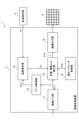
- FIG. (A) is a front view schematically showing a plurality of light emitting element units provided in the image display unit shown in FIG. 1, and (b) is an enlarged view schematically showing the structure of one light emitting element unit.
- FIG. (A) and (b) are diagrams showing an example of a change in luminance and a change in chromaticity depending on the temperature of a light emitting element.
- FIG. (A) and (b) are diagrams showing an operation example of the chromaticity / luminance unevenness correction unit shown in FIG.
- FIG. It is a figure which shows the example of the neural network which constitutes the temperature estimation part shown in FIG.
- FIG. 1 is a block diagram showing a configuration of an image display device 1 according to the first embodiment.
- the image display device 1 includes an image processing device 2 and a temperature measuring unit (for example, a temperature sensor that detects an environmental temperature which is an external temperature of the image display device 1) 3 for measuring air temperature. It has an image display unit 4 which is a display for displaying an image.
- the image processing device 2 can implement the image processing method according to the first embodiment.
- the image processing device 2 causes the image display unit 4 to display an image.
- the air temperature measuring unit 3 may be an external device configured to be able to communicate with the image display device 1. In this case, since the image display device 1 receives the air temperature measurement value Ta provided from the outside, it is not necessary to have the air temperature measurement unit 3.
- the image processing device 2 includes an image input unit 11, a data reduction unit 12, a temperature estimation unit 13, a correction parameter storage unit 14, a chromaticity / luminance unevenness correction unit 15, and an image. It has an output unit 16.
- the correction parameter storage unit 14 may be a storage device as an external configuration of the image processing device 2.
- the image input unit 11 and the image output unit 16 may have an external configuration of the image processing device 2.
- chromaticity / luminance means chromaticity and luminance, or luminance, or chromaticity. That is, “chromaticity / luminance” means at least one of chromaticity and luminance.
- chromaticity / luminance unevenness means chromaticity unevenness and luminance unevenness, luminance unevenness, or luminance unevenness. That is, “chromaticity / luminance unevenness” means at least one of chromaticity unevenness and luminance unevenness.
- FIG. 2A is a front view schematically showing a plurality of light emitting element units 40 provided in the image display unit 4 shown in FIG. 1, and FIG. 2B is a front view schematically showing one light emitting element unit 40. It is an enlarged view which shows the structure roughly.
- xmax pieces are used in the horizontal scanning direction (horizontal direction in FIG. 2A), and y in the vertical scanning direction (vertical direction in FIG. 2A).
- the max number of light emitting element units 40 are regularly arranged (for example, in a matrix).
- x max and y max are predetermined positive integers.
- Each light emitting element unit 40 has, for example, an LED chip as a light emitting element that emits red (R), green (G), and blue (B) light.
- the LED chips that emit R, G, and B light are also referred to as “LED chip for R”, “LED chip for G”, and “LED chip for B”, respectively. Further, the LED that emits R, G, and B light is also referred to as "LED chip for R, G, and B".
- each light emitting element unit (that is, each pixel) 40 has an LED chip for R, an LED chip for G, and B in one package. It has a structure provided with an LED chip for the purpose.
- the structure of the light emitting element unit 40 is not limited to the above, and may be any one having one or more light emitting elements. When one light emitting element unit 40 has one light emitting element, the light emitting element unit 40 and the light emitting element are the same.
- FIG. 3 (a) and 3 (b) are diagrams showing an example of changes in brightness and chromaticity of light generated in the light emitting element unit 40 having LEDs for R, G, and B depending on the temperature.
- FIG. 3A is a graph showing the luminance ratio (that is, the normalized value of luminance) Vp, which is the ratio of the luminance at the temperature T to the luminance, which is the luminance at the reference temperature Tr.
- FIG. 3B is a graph showing the chromaticity ratio (that is, the normalized value of the chromaticity) which is the ratio of the chromaticity at the temperature T to the reference chromaticity which is the chromaticity at the reference temperature Tr. As shown in FIGS.
- both or one of the brightness and chromaticity of the generated light depends on the temperature T. Change.
- the luminance ratio Vp decreases as the temperature T increases.
- the chromaticity is represented by, for example, the X stimulation value Xp and the Y stimulation value Yp of the CIE-XYZ color system.
- FIG. 3B shows changes in the X stimulus value Xp, which is the chromaticity ratio, and the Y stimulus value Yp, which is the chromaticity ratio.
- the X stimulation value Xp and the Y stimulation value Yp decrease as the temperature T increases.
- the image processing device 2 causes the image display unit 4 to display an image corresponding to the input image data.
- the image processing device 2 estimates and estimates the temperature of each light emitting element unit 40 (that is, the pixels of the coordinates (x, y)) of the image display unit 4 or the temperature of each of the LEDs based on the input image data.
- the temperature estimated value D13 also referred to as “Te” or “Te (x, y)”
- the image data for compensating for the change in chromaticity is corrected (for example, the image data for each pixel is corrected), and the corrected image data is supplied to the image display unit 4.
- the image processing device 2 may be partially or wholly composed of a processing circuit.
- the functions of the plurality of parts of the image processing device 2 may be realized by separate processing circuits, or the functions of the plurality of parts of the image processing device 2 may be collectively realized by one processing circuit. ..
- the processing circuit may be configured by hardware or may be configured by a computer that executes a program as software.
- a part of the functions of the image processing device 2 may be realized by hardware, and the other part may be realized by a computer that executes a program as software.
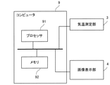
- FIG. 4 is a block diagram showing a computer 9 that realizes the functions of the image processing device 2 together with an image display unit 4 and an air temperature measurement unit 3.
- the computer 9 has a processor 91 as an information processing unit and a memory 92 as a storage unit.
- the processor 91 includes, for example, a CPU (Central Processing Unit), a GPU (Graphics Processing Unit), a microprocessor, a microcontroller, a DSP (Digital Signal Processor), and the like.
- a CPU Central Processing Unit
- GPU Graphics Processing Unit
- microprocessor a microcontroller
- DSP Digital Signal Processor
- the memory 92 is, for example, a RAM (Random Access Memory), a ROM (Read Only Memory), a flash memory, an EPROM (Erasable Programmable Read Only Memory), or an EPROM (Electrically Memory Memory) with an EPROM (Electrically Memory) .
- the memory 92 may include a magnetic disk, an optical disk, a magneto-optical disk, or the like.
- the processor 91 realizes the function of the image processing device 2 by executing the image processing program stored in the memory 92.
- the function of the image processing device 2 includes the control of the display operation in the image display unit 4.
- the computer 9 shown in FIG. 4 includes a single processor 91, but may include two or more processors.
- the image input unit 11 shown in FIG. 1 is a digital interface that receives digital image data and outputs n-bit (n is a positive integer) digital image data.
- the image input unit 11 receives digital image data and outputs the image data D11 to the data reduction unit 12 and the chromaticity / luminance unevenness correction unit 15.
- D11 is also written as "D11 (x, y)".
- D11 (x, y) means the image data of the pixel of the coordinate (x, y).
- the image input unit 11 may be an A / D (analog / digital) converter that converts an analog image signal into digital image data.
- FIG. 5 is a diagram showing an operation example of the data reduction unit 12.
- the data reduction unit 12 reduces the gradation of the image data D11 for each pixel to generate the image data D12 with the gradation reduced.
- D12 is also written as "D12 (x, y)".
- D12 (x, y) means image data in which the gradation of the pixel of the coordinate (x, y) is reduced.
- the data reduction unit 12 performs an operation represented by the equation (1), for example.
- X is the input data (8 bits) of a certain pixel in the image data D11 input to the data reduction unit 12
- Y is the gradation-reduced image data D12 output from the data reduction unit 12. Is the output data (6 bits) of the corresponding pixel in.
- the formula (1) is an image data D12 (that is, output data) output from the data reduction unit 12 with respect to a first value indicating the gradation of the image data D11 (that is, input data) input to the data reduction unit 12.
- the data retention rate which is the ratio of the second value indicating the gradation of), is higher as the gradation of the image data D11 input to the data reduction unit 12 is lower.
- the characteristics of the data reduction unit 12 are not limited to those shown in the equation (1) and FIG. However, it is desirable that the lower the gradation of the input image data D11, the higher the maintenance rate of the output image data D12. If it is not necessary to reduce the amount of data processed by the temperature estimation unit 13, the data reduction unit 12 can be omitted.
- the temperature estimation unit 13 shown in FIG. 1 is based on the temperature measurement value Ta output from the temperature measurement unit 3 and the image data D12 whose gradation is reduced for each pixel, and the temperature of each of the plurality of light emitting element units 40. Alternatively, the temperature of each of the LEDs is estimated, and the temperature estimation value Te indicating the estimated temperature is output. Te is also written as "Te (x, y)". Te (x, y) means the temperature estimate of the pixel at the coordinates (x, y).
- the chromaticity / luminance unevenness correction unit 15 shown in FIG. 1 is based on the temperature estimation value Te so that at least one unevenness of brightness and chromaticity due to temperature is compensated for each of the plurality of light emitting element units 40.
- the image data D11 is corrected.
- the temperature estimation unit 13 uses a trained neural network model formula for associating the gradation-reduced image data D12, the temperature measurement value Ta, and the respective temperatures of the light emitting element unit 40 with each other of the light emitting element unit 40.
- the temperature estimation value Te indicating the temperature is calculated.
- the parameter of the model formula stored in the correction parameter storage unit 14 is a value obtained by learning from the result of measuring the input / output relationship of the model formula in advance.
- the temperature estimation unit 13 estimates the individual temperature of each light emitting element unit 40 of the image display unit 4 or the temperature of each LED based on the gradation-reduced image data D12 and the temperature measurement value Ta.
- the estimated value Te is output to the chromaticity / luminance unevenness correction unit 15.
- the temperature estimation unit 13 is composed of, for example, a multi-layer neural network.
- FIG. 6 is a diagram showing an example of a neural network 13N constituting the temperature estimation unit 13.
- the neural network 13N shown in FIG. 6 has an input layer 131, an intermediate layer (that is, a hidden layer) 132, and an output layer 133.
- the number of intermediate layers is 3, but the number of intermediate layers may be 2 or less or 4 or more.
- Each of the neurons P of the input layer 131 is assigned the lighting rate of the LED to be measured, the temperature measurement value Ta, and the reduced image data D12.
- Each of the neurons P of the input layer 131 has any of the lighting rate of the LED to be measured, the temperature measurement value Ta, the reduced image data D12, and the past temperature estimation value (for example, the temperature estimation value one frame before). May be assigned.
- One of the temperature estimated value Te and the image data (that is, the pixel value) of each of the plurality of light emitting element units 40 is assigned to each of the plurality of light emitting element units 40, and each neuron P is assigned. Values (lighting rate, temperature measurement, temperature estimation, and image data) are input.
- the neuron P of the input layer 131 outputs the input as it is.
- the neuron P of the output layer 133 is composed of a plurality of bits, for example, 10 bits, and outputs data indicating the temperature estimation value Te of the selected light emitting element unit.
- Each of the neurons P in the intermediate layer 132 and the output layer 133 performs an operation represented by the following model formula (2) for a plurality of inputs.
- N is the number of inputs to neuron P.
- the number of inputs to neuron P is not always the same among neurons.
- x 1 to x N indicate the input data of the neuron P
- w 1 to w N indicate the weight for the input data x 1 to x N
- b indicates the bias.
- the weights w 1 to w N and the bias b are determined by learning. Further, the weights w1 to wN and the bias b are collectively referred to as parameters.
- the function s (a) is an activation function.
- the activation function may be, for example, a step function that outputs 0 if a is 0 or less, and outputs 1 otherwise.
- the activation function s (a) may be a ReLU (Rectifier Liner Unit) function that outputs 0 if a is 0 or less, and outputs an input value a otherwise, and the input value a is used as it is. It may be an equal function as an output value, or it may be a jigmoid function.
- the activation function used by the neuron P of the input layer 131 is an identity function.
- the step function or the jigmoid function may be used in the intermediate layer 132, and the ReLU function may be used in the output layer.
- different activation functions may be used between neurons P in the same layer.
- the number of neurons P and the number of layers are not limited to the example shown in FIG.
- the method of calculating the weight parameter of the temperature estimation unit 13 will be described.
- a plurality of patterns of input / output data of the temperature estimation unit 13 are measured in advance, and the difference between the output value (estimated value) in each input pattern and the measured value of the actual temperature is calculated.
- the weight parameters are learned so that the difference between the measured value and the estimated value in all patterns is minimized.
- the calculation method is not limited to this. Any value may be used as long as it is a value calculated in advance from the input / output data of the temperature estimation unit 13.
- the correction parameter storage unit 14 stores correction parameters for correcting changes in luminance and chromaticity due to temperature.
- the chromaticity / luminance unevenness correction unit 15 refers to the correction parameters stored in the correction parameter storage unit 14 according to the temperature estimated by the temperature estimation unit 13, and the image data supplied from the image input unit 11. To correct. This correction is performed for each R, G, B pixel. This correction is a correction for canceling changes in luminance and chromaticity due to changes in the temperature of the light emitting element unit 40.
- 7 (a) and 7 (b) show an example of the relationship between the input and the output defined by the correction parameter stored in the correction parameter storage unit 14.
- the relationship between the input and the output here is expressed by the ratio of the output to the input, that is, a coefficient. This coefficient is called a correction coefficient.
- the compensation table for luminance is the one having the input-output relationship exemplified in FIG. 7 (a), that is, the temperature. It is memorized that the change with respect to the rise is opposite to that in FIG. 7 (a).
- the compensation table is configured by the compensation coefficient Vq equal to the reciprocal of the normalized value of the luminance ratio Vp.
- the normalized value referred to here is a ratio to the brightness at the reference temperature.
- the correction parameter is the input-output relationship exemplified in FIG. 7 (b). That is, the one having the above, that is, the one in which the change with respect to the increase in temperature is opposite to that in FIG. 3 (b) is stored.
- the correction parameter of the X stimulus value is configured by the compensation coefficient Xq equal to the reciprocal of the normalized value of the X stimulus value Xp.
- the correction parameter of the Y stimulation value is configured by the compensation coefficient Yq equal to the reciprocal of the normalized value of the Y stimulation value Yp.
- the normalized value referred to here is a ratio to the X stimulation value and the Y stimulation value at the reference temperature.
- the correction parameter storage unit 14 may hold the chromaticity correction parameter as a correction parameter based on the chromaticity ratio, or may hold the correction parameter for converting each of R, G, and B.
- a value representing an average change is used as a curve showing the luminance and chromaticity of FIGS. 3 (a) and 3 (b).
- a correction parameter representing the compensation coefficients in FIGS. 7 (a) and 7 (b) is created to compensate for such an average change. Will be done.
- the correction parameter is set to the average value, but the present embodiment is not limited to this. Parameters may be set for each light emitting element.
- the correction parameter has a compensation coefficient value for each of the possible values of the temperature of the light emitting element, but is not limited to this. That is, for the temperature of the light emitting element which has the value of the compensation coefficient discretely with respect to the temperature of the light emitting element and does not have the value of the compensation coefficient, the value of the corresponding compensation coefficient may be obtained by interpolation. This interpolation can be performed, for example, by using the value of the compensation coefficient corresponding to the temperature value (table point) having the value of the compensation coefficient.
- the correction parameters may be different for each of the light emitting elements of R, G, and B.
- the image output unit 16 converts the image data D15 output from the chromaticity / luminance unevenness correction unit 15 into a signal in a format that matches the display method of the image display unit 4, and outputs the converted image signal D16. For example, when the light emitting element unit of the image display unit 4 emits light by PWM (Pulse Width Modulation) drive, the image output unit 16 converts the gradation value of the image data into a PWM signal.
- PWM Pulse Width Modulation
- the image display unit 4 displays an image based on the image signal received from the image processing device 2.
- changes in brightness and chromaticity due to temperature are compensated for each light emitting element unit (that is, a pixel) or for each LED (that is, a sub-pixel). Therefore, the uneven brightness and uneven chromaticity of the image displayed on the image display unit 4 are reduced.
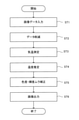
- FIG. 8 is a flowchart showing an image processing method implemented by the image processing device 2.
- the processing shown in FIG. 8 indicates the processing by the processor 91.
- step ST1 when the image data is input to the image input unit 11, the process by the image input unit 11 is executed.
- steps ST2 and ST3 the data reduction unit 12 reduces the data and measures the temperature.
- the temperature estimation unit 13 estimates the temperature of each light emitting element unit 40.
- step ST5 the estimated temperature value is stored in the estimated temperature storage unit 17.
- step ST6 the chromaticity / luminance unevenness correction unit 15 corrects the brightness and the chromaticity, and the image data is output from the image output unit 16.
- FIG. 9 is a block diagram showing the image display device according to the first embodiment together with the learning device 20, the trained model storage unit 23, and the learning temperature measuring unit 24.
- the learning device 20 has a data acquisition unit 22 and a model generation unit 21.
- the learning temperature measuring unit 24 has one or more temperature sensors. Each of the one or more temperature sensors is provided corresponding to one or more light emitting element units of the plurality of light emitting element units 40 constituting the image display unit 4, and each temperature sensor is provided with the corresponding light emitting element unit. The temperature of 40 is measured, and the temperature measurement values Tf (1), Tf (2), ... Are acquired.
- One or more light emitting element units to be measured for temperature are specified in advance.
- a light emitting element unit located in the center of the screen may be specified, or a light emitting element unit located between the center of the screen and the peripheral portion may be specified.
- the learning device 20 may be configured by a computer.
- the learning device 101 may be configured by the same computer.
- the computer constituting the learning device 101 may be, for example, the one shown in FIG. In that case, the function of the learning device 101 may be realized by the processor 91 executing the program stored in the memory 92.
- the learning device 20 operates a part of the image processing device 2, causes the temperature estimation unit 13 to estimate the temperature of the designated light emitting element unit, and the temperature estimation value Te (x d , y d ) is the temperature measurement for learning. Learning is performed so as to be close to the temperature measurement value Tf (x d , y d ) of the designated light emitting element unit obtained by the measurement of the unit 24.
- the model generation unit 21 stores the parameters of the equation (2), which is the result of learning, in the trained model storage unit 23.
- the parameters stored in the trained model storage unit 23 are provided in the correction parameter storage unit 14. Alternatively, the trained model storage unit 23 may be a part of the correction parameter storage unit 14.
- the temperature sensor of the learning temperature measuring unit 24 is removed, and the image display device 1 is used in a state where the temperature sensor is removed. That is, when used for image display, the image display device 1 does not require a temperature sensor for detecting the temperature of the light emitting element unit. This is because the temperature estimation unit 13 can estimate the temperature of the light emitting element unit or the temperature of each of the LEDs even if there is no temperature sensor for detecting the temperature of the light emitting element unit.
- the learning device 20 may be removed or may remain attached after learning is completed.
- the function of the learning device 101 is realized by executing a program by the processor 91, the program may remain stored in the memory 92.
- the temperature of each of the light emitting element units 40 or the temperature of each of the LEDs is estimated without the need for a temperature sensor for each LED, and the brightness unevenness and the chromaticity unevenness due to the temperature are estimated. One or both can be corrected.
- the calculation amount of the temperature estimation unit 13 can be reduced as compared with the case where the temperature estimation is performed with the input image without gradation reduction without using the data reduction unit.
- the data retention rate by the data reduction unit 12 is higher as the gradation of the image data D11 input to the data reduction unit 12 is lower. Therefore, the accuracy of the temperature estimation value Te at the time of low gradation can be improved.
- FIG. 10 is a block diagram showing the configuration of the image display device 1a according to the second embodiment.
- components that are the same as or correspond to the components shown in FIG. 1 are designated by the same reference numerals as those shown in FIG.
- the image display device 1a according to the second embodiment is different from the image display device 1 according to the first embodiment in the points shown in the following (E1) to (E3).
- the image processing device 2a has an estimated temperature storage unit 17 that stores the temperature estimated by the temperature estimation unit 13a as a past temperature estimation value Tp.
- the temperature estimation unit 13a of the image processing apparatus 2a has one or more past times (preferably, a plurality of times) stored in the temperature measurement value Ta, the image data D12 with reduced gradation, and the estimated temperature storage unit 17.
- the temperature of each of the plurality of light emitting element units 40 that is, the temperature of each pixel is estimated based on the temperature estimation value Tp of (time). This process is performed, for example, as shown in (E3) below.
- the temperature estimation unit 13a of the image processing apparatus 2a has the temperature estimation value Tp of one or more past times stored in the gradation-reduced image data D12, the temperature measurement value Ta, and the estimation temperature storage unit 17. Using the model formula of the trained neural network that associates the temperature estimated value Te of each of the light emitting element units 40 with the temperature estimated value Te of each of the light emitting element units 40, the temperature estimated value Te of each of the light emitting element units 40, that is, the temperature of each pixel is calculated.
- FIG. 11 is a diagram showing an example of the neural network 13Na constituting the temperature estimation unit 13a shown in FIG.
- the neural network 13Na is a model formula of a multi-layer neural network that inputs image data N12 with reduced gradation, temperature measurement value Ta, and temperature estimation value Tp at multiple times in the past, and outputs the temperature of each LED of the image display unit 4. It has become.
- the neural network 13Na shown in FIG. 11 has an input layer 131a, an intermediate layer 132a, and an output layer 133a. In the illustrated example, the number of intermediate layers 132a is 3, but the number of intermediate layers 132a may be 2 or less or 4 or more.
- Each of the neurons P of the input layer 131a is assigned one of the lighting rate of the LED to be measured, the temperature measurement value Ta, the gradation-reduced image data D12, and the past temperature estimation value Tp.
- One of the temperature estimated value Te and the image data (that is, the pixel value) of each of the plurality of light emitting element units 40 is assigned to each of the plurality of light emitting element units 40, and each neuron P is assigned.
- Values (lighting rate, temperature measurement, temperature estimation, and image data) are input.
- the neuron P of the input layer 131a outputs the input as it is.
- the neuron P of the output layer 133a is composed of a plurality of bits, for example, 10 bits, and outputs data indicating the temperature estimation value Te (x, y) of the selected light emitting element unit.
- Each of the neurons P in the intermediate layer 132a and the output layer 133a performs an operation represented by the following model formula (3) for a plurality of inputs.
- N is the number of inputs to neuron P.
- the number of inputs to neuron P is not necessarily the same among neurons.
- x 1 to x N indicate the input data of the neuron P
- w 1 to w N indicate the weight for the input data x 1 to x N
- b indicates the bias.
- the weights w 1 to w N and the bias b are determined by learning. Equation (3) is the same as the above equation (2) in terms of notation, but the actual values of the weights w1 to wN and the bias b are different.
- FIG. 12 is a flowchart showing an image processing method implemented by the image processing device 2a.
- the same or corresponding step as the step shown in FIG. 8 is designated by the same reference numeral as that shown in FIG.
- the temperature estimated by the temperature estimation unit 13a is stored in the estimated temperature storage unit 17 as the past temperature estimation value Tp in step ST7, and the temperature measurement value Ta and the gradation are stored in step ST4a.
- the image processing method according to the first embodiment is different from the image processing method according to the first embodiment in that the temperature of each of the plurality of light emitting element units 40 is estimated based on the reduced image data D12 and the past temperature estimation value Tp.
- the second embodiment it is not necessary to provide a temperature sensor for each of the light emitting element units 40 or each LED, and the temperature of each LED is estimated, and one of the luminance unevenness and the chromaticity unevenness due to the temperature, or one of them. Both can be corrected.
- the calculation amount of the temperature estimation unit 13 can be reduced as compared with the case where the temperature estimation is performed with the input image without gradation reduction without using the data reduction unit.
- the data retention rate by the data reduction unit 12 is higher as the gradation of the image data D11 input to the data reduction unit 12 is lower. Therefore, the accuracy of the temperature estimation value Te at the time of low gradation can be improved.
- the temperature estimation unit 13a can use the temperature estimation value Tp at one or more times in the past, so that the accuracy of the temperature estimation value Te can be improved.
Abstract
画像処理装置(2)は、画像データ(D11)の階調を画素ごとに削減して、階調削減された画像データ(D12)を生成するデータ削減部(12)と、気温測定値(Ta)と階調削減された画像データ(D12)とに基づいて、複数の発光素子部の各々の温度を推定する温度推定部(13)と、複数の発光素子部(40)の各々について、温度による輝度及び色度の少なくとも一方のムラが補償されるように、温度推定値(Te)に基づいて画像データ(D11)を補正する色度・輝度ムラ補正部(15)とを有し、温度推定部(13)は、階調削減された画像データ(D12)と気温測定値(Ta)と複数の発光素子部の各々の温度とを対応付ける学習済みニューラルネットワークのモデル式を用いて、複数の発光素子部の各々の温度を示す温度推定値(Te)を算出し、モデル式のパラメータは、予めモデル式の入出力の関係を計測した結果から学習して得られた値である。
Description
本開示は、画像処理装置、画像表示装置、画像処理方法、及び画像処理プログラムに関する。
特許文献1は、バックライトにLED(Light Emitting Diode)が用いられた液晶表示パネルの温度を測定し、測定された温度に応じた補正データを用いて画像データを補正する液晶表示パネルの駆動方法を提案している。
また、赤(R)、緑(G)及び青(B)の光を発する3個のLEDを有する1つの発光素子部(「3in1チップタイプのLED素子」とも称される。)を1画素とし、複数の画素が規則的に配置された画像表示ユニットを複数個連結して1画面を構成する表示パネルが実用されている。また、一般的に、LEDなどの発光素子で発生する光の輝度及び色度は温度に応じて変化する。このため、表示パネルでは、輝度ムラ及び色度ムラが発生する。
しかしながら、1つの発光素子部を1画素とする表示パネルでは、表示コンテンツ(すなわち、入力画像データ)によって、個々の発光素子に流れる電流が変わるため、個々の発光素子の温度が異なる。発光素子は温度によって色度及び輝度が変化するため、画像に輝度ムラ及び色度ムラが発生する。
本開示の目的は、画像表示部に表示される画像の輝度ムラ及び色度ムラの少なくとも一方を低減することである。
本開示の一態様に係る画像処理装置は、複数の発光素子部を有し、前記複数の発光素子部の各々が1つ以上の発光素子を含む、画像表示部に、画像を表示させる装置であって、画像データの階調を画素ごとに削減して、階調削減された画像データを生成するデータ削減部と、気温を測定する気温測定部から出力された気温測定値と前記階調削減された画像データとに基づいて、前記複数の発光素子部の各々の温度又は前記発光素子の各々の温度を推定し、推定された前記温度を示す温度推定値を出力する温度推定部と、前記複数の発光素子部の各々について、温度による輝度及び色度の少なくとも一方のムラが補償されるように、前記温度推定値に基づいて前記画像データを補正する色度・輝度ムラ補正部と、を有し、前記温度推定部は、前記階調削減された画像データと前記気温測定値と前記複数の発光素子部の各々の温度又は前記発光素子の各々の温度とを対応付ける学習済みニューラルネットワークのモデル式を用いて、前記複数の発光素子部の各々の温度を示す前記温度推定値を算出し、前記モデル式のパラメータは、予め前記モデル式の入出力の関係を計測した結果から学習して得られた値であることを特徴とする。
本開示の他の態様に係る画像処理方法は、複数の発光素子部を有し、前記複数の発光素子部の各々が1つ以上の発光素子を含む、画像表示部に、画像を表示させる画像処理方法であって、画像データの階調を画素ごとに削減して、階調削減された画像データを生成するステップと、気温を測定する気温測定部から出力された気温測定値と前記階調削減された画像データとに基づいて、前記複数の発光素子部の各々の温度又は前記発光素子の各々の温度を推定し、推定された前記温度を示す温度推定値を出力するステップと、前記複数の発光素子部の各々について、温度による輝度及び色度の少なくとも一方のムラが補償されるように、前記温度推定値に基づいて前記画像データを補正するステップと、を有し、前記温度推定値を出力するステップでは、前記階調削減された画像データと前記気温測定値と前記複数の発光素子部の各々の温度又は前記発光素子の各々の温度とを対応付ける学習済みニューラルネットワークのモデル式を用いて、前記複数の発光素子部の各々の温度を算出し、前記モデル式のパラメータは、予め前記モデル式の入出力の関係を計測した結果から学習して得られた値であることを特徴とする。
本開示の画像処理装置、画像表示装置、画像処理方法、及び画像処理プログラムのいずれかを用いれば、画像表示部に表示される画像の輝度ムラ及び色度ムラの少なくとも一方を低減することができる。
以下に、実施の形態に係る画像処理装置、画像表示装置、画像処理方法、及び画像処理プログラムを、図面を参照しながら説明する。以下の実施の形態は、例にすぎず、実施の形態を適宜組み合わせること及び各実施の形態を適宜変更することが可能である。
実施の形態1.
図1は、実施の形態1に係る画像表示装置1の構成を示すブロック図である。図1に示されるように、画像表示装置1は、画像処理装置2と、気温を測定する気温測定部(例えば、画像表示装置1の外部の温度である環境温度を検出する温度センサ)3と、画像を表示するディスプレイである画像表示部4とを有する。画像処理装置2は、実施の形態1に係る画像処理方法を実施することができる。画像処理装置2は、画像表示部4に画像を表示させる。気温測定部3は、画像表示装置1と通信可能に構成された、外部の装置であってもよい。この場合には、画像表示装置1は、外部から提供される気温測定値Taを受信するので、気温測定部3を有する必要はない。
図1は、実施の形態1に係る画像表示装置1の構成を示すブロック図である。図1に示されるように、画像表示装置1は、画像処理装置2と、気温を測定する気温測定部(例えば、画像表示装置1の外部の温度である環境温度を検出する温度センサ)3と、画像を表示するディスプレイである画像表示部4とを有する。画像処理装置2は、実施の形態1に係る画像処理方法を実施することができる。画像処理装置2は、画像表示部4に画像を表示させる。気温測定部3は、画像表示装置1と通信可能に構成された、外部の装置であってもよい。この場合には、画像表示装置1は、外部から提供される気温測定値Taを受信するので、気温測定部3を有する必要はない。
図1に示されるように、画像処理装置2は、画像入力部11と、データ削減部12と、温度推定部13と、補正パラメータ格納部14と、色度・輝度ムラ補正部15と、画像出力部16とを有する。補正パラメータ格納部14は、画像処理装置2の外部の構成としての記憶装置であってもよい。画像入力部11及び画像出力部16は、画像処理装置2の外部の構成であってもよい。
本出願において、「色度・輝度」とは、色度及び輝度、又は、輝度、又は、色度を意味する。すなわち、「色度・輝度」は、色度及び輝度の少なくとも一方を意味する。また、「色度・輝度ムラ」は、色度ムラ及び輝度ムラ、又は、輝度ムラ、又は、色度ムラを意味する。すなわち、「色度・輝度ムラ」は、色度ムラ及び輝度ムラの少なくとも一方を意味する。
図2(a)は、図1に示される画像表示部4に備えられた複数の発光素子部40を概略的に示す正面図であり、図2(b)は、1つの発光素子部40の構造を概略的に示す拡大図である。図2(a)に示されるように、画像表示部4では、水平走査方向(図2(a)における横方向)にxmax個、垂直走査方向(図2(a)における縦方向)にymax個の発光素子部40が規則的に(例えば、マトリックス状に)配置されている。xmax及びymaxは、予め定められた正の整数である。
各発光素子部40は、例えば、赤(R)、緑(G)及び青(B)の光を発する発光素子としてのLEDチップを有する。R、G、Bの光を発するLEDチップは、それぞれ「R用のLEDチップ」、「G用のLEDチップ」、「B用のLEDチップ」とも表記される。また、R、G、Bの光を発するLEDは、「R、G、B用のLEDチップ」とも表記される。図2(b)に符号R、G、Bで示されるように、各発光素子部(すなわち、各画素)40は、1つのパッケージ内にR用のLEDチップ、G用のLEDチップ、及びB用のLEDチップが設けられた構造を有している。ただし、発光素子部40の構造は、上記のものに限定されず、1つ以上の発光素子を有するものであればよい。1つの発光素子部40が1つの発光素子を有する場合は、発光素子部40と発光素子とは、同じものである。
図3(a)及び(b)は、R、G、B用のLEDを有する発光素子部40で発生する光の輝度及び色度の温度による変化の例を示す図である。図3(a)には、基準温度Trにおける輝度である基準輝度に対する温度Tにおける輝度の比である輝度比(すなわち、輝度の正規化値)Vpがグラフで示されている。図3(b)には、基準温度Trにおける色度である基準色度に対する温度Tにおける色度の比である色度比(すなわち、色度の正規化値)がグラフで示されている。図3(a)及び(b)に示されるように、R、G、B用のLEDを有する発光素子部40は、発生する光の輝度及び色度の双方又は一方が、温度Tに応じて変化する。図3(a)では、輝度比Vpは温度Tの上昇に応じて低下する。図3(b)では、色度は、例えば、CIE-XYZ表色系のX刺激値Xp及びY刺激値Ypで表される。図3(b)は、色度比であるX刺激値Xp及び色度比であるY刺激値Ypの変化を示す。図3(b)では、X刺激値Xp及びY刺激値Ypは、温度Tの上昇に応じて低下する。
画像処理装置2は、入力画像データに応じた画像を画像表示部4に表示させる。画像処理装置2は、入力画像データに基づいて、画像表示部4の各発光素子部40(すなわち、座標(x,y)の画素)の温度又はLEDの各々の温度を推定し、推定された温度である温度推定値D13(「Te」又は「Te(x,y)」とも表記する。)に基づいて、温度変化による座標(x,y)の発光素子部40で発生する光の輝度及び色度の変化を補償するための画像データの補正(例えば、画素ごとの画像データの補正)を行い、補正された画像データを画像表示部4に供給する。
画像処理装置2は、その一部又は全部を処理回路で構成し得る。例えば、画像処理装置2の複数の部分の機能をそれぞれ別個の処理回路で実現してもよく、又は、画像処理装置2の複数の部分の機能を纏めて1つの処理回路で実現してもよい。処理回路は、ハードウェアで構成されてもよく、ソフトウェアとしてのプログラムを実行するコンピュータで構成されてもよい。画像処理装置2の機能のうちの一部をハードウェアで実現し、他の部分をソフトウェアとしてのプログラムを実行するコンピュータで実現してもよい。
図4は、画像処理装置2の機能を実現するコンピュータ9を、画像表示部4及び気温測定部3とともに示すブロック図である。コンピュータ9は、情報処理部としてのプロセッサ91と、記憶部としてのメモリ92とを有する。
プロセッサ91は、例えば、CPU(Central Processing Unit)、GPU(Graphics Processing Unit)、マイクロプロセッサ、マイクロコントローラ又はDSP(Digital Signal Processor)などを備える。
メモリ92は、例えば、RAM(Random Access Memory)、ROM(Read Only Memory)、フラッシュメモリ、EPROM(Erasable Programmable Read Only Memory)若しくはEEPROM(Electrically Erasable Programmable Read Only Memory)等の半導体メモリを有している。メモリ92は、磁気ディスク、光ディスク、又は、光磁気ディスク等を有してもよい。
プロセッサ91は、メモリ92に記憶されている画像処理プログラムを実行することにより、画像処理装置2の機能を実現する。画像処理装置2の機能には、画像表示部4における表示動作の制御が含まれる。なお、図4に示されるコンピュータ9は、単一のプロセッサ91を含むが、2つ以上のプロセッサを含んでいてもよい。
図1に示される画像入力部11は、デジタル画像データを受信して、nビット(nは正の整数)のデジタル画像データを出力するデジタルインターフェースである。画像入力部11は、デジタルの画像データを受信して、データ削減部12及び色度・輝度ムラ補正部15に画像データD11を出力する。D11は、「D11(x,y)」とも表記される。D11(x,y)は、座標(x,y)の画素の画像データを意味する。なお、画像入力部11は、アナログの画像信号をデジタルの画像データに変換するA/D(アナログ・デジタル)変換器であってもよい。
図5は、データ削減部12の動作例を示す図である。データ削減部12は、画像データD11の階調を画素ごとに削減して、階調削減された画像データD12を生成する。D12は、「D12(x,y)」とも表記される。D12(x,y)は、座標(x,y)の画素の階調削減された画像データを意味する。データ削減部12は、例えば、式(1)で表される演算を行う。

ここで、Xは、データ削減部12に入力される画像データD11における、ある画素の入力データ(8ビット)であり、Yは、データ削減部12から出力される階調削減された画像データD12における、対応する画素の出力データ(6ビット)である。
式(1)は、データ削減部12に入力される画像データD11(すなわち、入力データ)の階調を示す第1の値に対する、データ削減部12から出力される画像データD12(すなわち、出力データ)の階調を示す第2の値の割合であるデータの維持率は、データ削減部12に入力される画像データD11の階調が低いほど、高い。データ削減部12の特性は、式(1)及び図5に示されるものに限定されない。ただし、入力される画像データD11の階調が低いほど、出力される画像データD12の維持率が高いことが望ましい。なお、温度推定部13によるデータ処理量の低減が必要でない場合には、データ削減部12を省略することが可能である。
図1に示される温度推定部13は、気温測定部3から出力された気温測定値Taと画素ごとに階調削減された画像データD12とに基づいて、複数の発光素子部40の各々の温度又はLEDの各々の温度を推定し、推定された温度を示す温度推定値Teを出力する。Teは、「Te(x,y)」とも表記される。Te(x,y)は、座標(x,y)の画素の温度推定値を意味する。
図1に示される色度・輝度ムラ補正部15は、複数の発光素子部40の各々について、温度による輝度及び色度の少なくとも一方のムラが補償されるように、温度推定値Teに基づいて画像データD11を補正する。
温度推定部13は、階調削減された画像データD12と気温測定値Taと発光素子部40の各々の温度とを対応付ける学習済みニューラルネットワークのモデル式とを用いて、発光素子部40の各々の温度を示す温度推定値Teを算出する。補正パラメータ格納部14に格納されている、モデル式のパラメータは、予めモデル式の入出力の関係を計測した結果から学習して得られた値である。
温度推定部13は、階調削減された画像データD12及び気温測定値Taとに基づいて画像表示部4の各発光素子部40の個々の温度又はLED個々の温度を推定して得られた温度推定値Teを、色度・輝度ムラ補正部15へ出力する。温度推定部13は、例えば、多層ニューラルネットワークで構成されている。
図6は、温度推定部13を構成するニューラルネットワーク13Nの例を示す図である。図6に示されるニューラルネットワーク13Nは、入力層131と、中間層(すなわち、隠れ層)132と、出力層133とを有する。図示の例では、中間層の数が3であるが、中間層の数は、2以下であってもよく、4以上であってもよい。
入力層131のニューロンPの各々には、測定対象のLEDの点灯率、気温測定値Ta、削減された画像データD12が割り当てられる。入力層131のニューロンPの各々には、測定対象のLEDの点灯率、気温測定値Ta、削減された画像データD12、及び過去の温度推定値(例えば、1フレーム前の温度推定値)のいずれかが割り当てられてもよい。複数の発光素子部40のそれぞれには、温度推定値Te、及び複数の発光素子部40のそれぞれの画像データ(すなわち、画素値)のいずれかが割り当てられ、各ニューロンPには、割り当てられた値(点灯率、気温測定値、温度推定値、及び画像データ)が入力される。入力層131のニューロンPは、入力をそのまま出力する。
出力層133のニューロンPは、複数のビット、例えば、10ビットから成り、選択されている発光素子部の温度推定値Teを示すデータを出力する。
中間層132及び出力層133のニューロンPの各々は、複数の入力に対して下記のモデル式である式(2)で表される演算を行う。
式(2)において、Nは、ニューロンPへの入力の数である。ニューロンPへの入力の数は、ニューロン相互間で同じであるとは限らない。式(2)において、x1~xNは、ニューロンPの入力データ、w1~wNは、入力データx1~xNに対する重み、bは、バイアスを示す。重みw1~wN及びバイアスbは、学習により定められる。また、重みw1~wN及びバイアスbを纏めてパラメータとも言う。
関数s(a)は、活性化関数である。活性化関数は、例えば、aが0以下であれば0を出力し、それ以外であれば1を出力するステップ関数であってもよい。活性化関数s(a)は、aが0以下であれば0を出力し、それ以外であれば入力値aを出力するReLU(Rectified Linear Unit)関数であってもよく、入力値aをそのまま出力値とする恒等関数でもよく、ジグモイド関数であってもよい。
上記のように、入力層131のニューロンPは、入力をそのまま出力するものであるので、入力層131のニューロンPで用いられる活性化関数は、恒等関数である。
例えば、中間層132では、ステップ関数又はジグモイド関数を用い、出力層ではReLU関数を用いてもよい。また、同じ層内のニューロンPの相互間で異なる活性化関数が用いられていてもよい。なお、ニューロンPの数、層の数(すなわち、段階数)は、図6に示される例に限定されない。
温度推定部13の重みパラメータの算出方法を説明する。予め温度推定部13の入出力のデータを複数パターン測定し、各入力パターンにおける出力値(推定値)と実際の温度の測定値の差を算出する。全てのパターンにおける測定値と推定値の差が最小になるように重みパラメータを学習する。算出方法は、これに限定しない。予め温度推定部13の入出力データから算出した値であればよい。
補正パラメータ格納部14は、温度による輝度及び色度の変化を補正するための補正パラメータを格納している。
色度・輝度ムラ補正部15は、温度推定部13で推定された温度に応じて、補正パラメータ格納部14に格納されている補正パラメータを参照して、画像入力部11から供給される画像データを補正する。この補正は、R,G,B画素毎に行われる。この補正は、発光素子部40の温度の変化による輝度及び色度の変化を打ち消すための補正である。
図7(a)及び(b)は、補正パラメータ格納部14に格納されている補正パラメータで定義される入力と出力との関係の一例を示す。ここで言う入力と出力との関係は、入力に対する出力の比、すなわち係数で表される。この係数を補正係数と言う。
例えば、温度による輝度の変化が、図3(a)に示す如くである場合、輝度についての補償テーブルとしては、図7(a)に例示される入力-出力関係を有するもの、すなわち、温度の上昇に対する変化が、図7(a)とは逆向きであるものが記憶されている。例えば、輝度比Vpの正規化値の逆数に等しい補償係数Vqにより補償テーブルが構成されている。ここで言う、正規化値は、基準温度における輝度に対する比である。
同様に、温度による色度を表すX刺激値及びY刺激値の変化が、図3(b)に示す如くである場合、補正パラメータとしては、図7(b)に例示される入力-出力関係を有するもの、すなわち、温度の上昇に対する変化が、図3(b)とは、逆向きであるものが記憶されている。
例えば、X刺激値Xpの正規化値の逆数に等しい補償係数XqによりX刺激値の補正パラメータが構成されている。同様に、Y刺激値Ypの正規化値の逆数に等しい補償係数YqによりY刺激値の補正パラメータが構成されている。ここで言う、正規化値は、基準温度におけるX刺激値及びY刺激値に対する比である。
補正パラメータ格納部14は、色度の補正パラメータは、色度比を基準とした補正パラメータとして保持してもよいし、R,G,Bそれぞれを変換する補正パラメータで保持していてもよい。
発光素子相互間では、温度による輝度及び色度の変化の仕方が異なる可能性がある。その場合には、図3(a)及び(b)の輝度及び色度を示す曲線として、平均的な変化を表す値が用いられる。例えば、多数の発光素子についての変化を平均した値が用いられ、図7(a)及び(b)の補償係数を表す補正パラメータとして、そのような平均的な変化を補償するためのものが作成される。
発光素子相互間では、温度による輝度及び色度の変化の仕方が異なる場合、補正パラメータへは平均値としたが、本実施の形態は、これに限定されない。発光素子ごとにパラメータを設定してもよい。
補正パラメータは、発光素子の温度が取り得る値の各々に対して、補償係数の値を持つものとしているが、これに限定されない。すなわち、発光素子の温度につき、離散的に補償係数の値を持ち、補償係数の値を持たない発光素子の温度については、補間によって対応する補償係数の値を求めてもよい。この補間は、例えば、補償係数の値を持つ温度の値(テーブル点)に対応する補償係数の値を用いて行うことができる。
補正パラメータは、R,G,Bの発光素子ごとに異なる補正パラメータでもよい。
画像出力部16は、色度・輝度ムラ補正部15から出力された画像データD15を、画像表示部4の表示方式に合致したフォーマットの信号に変換し、変換後の画像信号D16を出力する。例えば、画像表示部4の発光素子部がPWM(Pulse Width Modulation)駆動によって発光する場合には、画像出力部16は、画像データの階調値をPWM信号に変換する。
画像表示部4は、画像処理装置2から受け取った画像信号に基づいて画像を表示する。表示される画像は、温度による輝度及び色度の変化が発光素子部(すなわち、画素)ごとに又はLED(すなわち、副画素)ごとに補償されたものとなる。したがって、画像表示部4に表示される画像の輝度ムラ及び色度ムラが低減される。
図8は、画像処理装置2によって実施される画像処理方法を示すフローチャートである。画像処理装置2が図4に示されるコンピュータ9で構成されている場合、図8に示される処理はプロセッサ91による処理を示す。
図8に示される処理は、フレーム期間ごとに行われる。ステップST1では、画像データが画像入力部11に入力されると、画像入力部11による処理が実行される。ステップST2及びST3では、データ削減部12によるデータの削減及び気温の測定が行われる。ステップST4では、温度推定部13によって各発光素子部40の温度の推定が行われる。
ステップST5では、推定温度格納部17に、温度推定値が格納される。この処理と並行して、ステップST6では、色度・輝度ムラ補正部15によって輝度及び色度の補正が行われ、画像出力部16から画像データが出力される。
図9は、実施の形態1に係る画像表示装置を、学習装置20、学習済モデル記憶部23、及び学習用温度測定部24とともに示すブロック図である。学習装置20は、データ取得部22と、モデル生成部21とを有する。
学習用温度測定部24は、1以上の温度センサを有する。1以上の温度センサはそれぞれ、画像表示部4を構成する複数の発光素子部40うちの1以上の発光素子部に対応して設けられたものであり、各温度センサは、対応する発光素子部40の温度を測定して、温度測定値Tf(1),Tf(2),…を取得する。
温度測定の対象となる1以上の発光素子部は、予め指定される。1つの発光素子部を指定する場合、例えば、画面の中央に位置する発光素子部を指定してもよく、画面の中央と周辺部との中間に位置する発光素子部を指定してもよい。
学習装置20は、コンピュータで構成されていてもよい。画像処理装置2がコンピュータで構成される場合、同じコンピュータで学習装置101が構成されていてもよい。学習装置101を構成するコンピュータは、例えば、図3に示されるものであってもよい。その場合、学習装置101の機能は、プロセッサ91がメモリ92に記憶されているプログラムを実行することで実現されるものであってもよい。
学習装置20は、画像処理装置2の一部を動作させ、温度推定部13に、上記指定発光素子部の温度を推定させ、温度推定値Te(xd,yd)が、学習用温度測定部24の測定で得られた指定発光素子部の温度測定値Tf(xd,yd)に近くなるように学習を行う。モデル生成部21は、学習の結果である式(2)のパラメータを学習済モデル記憶部23に格納する。学習済モデル記憶部23に格納されパラメータは、補正パラメータ格納部14に提供される。或いは、学習済モデル記憶部23は、補正パラメータ格納部14の一部であってもよい。
学習が終了した後、学習用温度測定部24の温度センサは、取り外され、画像表示装置1は、該温度センサが取り外された状態で使用される。すなわち、画像表示のために利用される際は、画像表示装置1は、発光素子部の温度を検知する温度センサを必要としない。発光素子部の温度を検知する温度センサがなくても、温度推定部13で発光素子部の温度又はLEDの各々の温度を推定し得るからである。
学習装置20は、学習が終了した後に、取り外されてもよく、装着されたままであってもよい。特に、学習装置101の機能がプロセッサ91によるプログラムの実行によって実現される場合には、該プログラムは、メモリ92に記憶されたままであってもよい。
以上に説明したように、実施の形態1では、LED個々に温度センサを必要とせずに、発光素子部40の各々の温度又はLEDの各々の温度を推定し、温度による輝度ムラ及び色度ムラの一方又は両方を補正することができる。
また、データ削減部12を有することで、データ削減部を用いずに温度推定を階調削減しない入力画像で行った場合に比べて、温度推定部13の演算量を削減することができる。
また、データ削減部12によるデータの維持率は、データ削減部12に入力される画像データD11の階調が低いほど、高い。このため、低い階調時における温度推定値Teの精度を向上できる。
実施の形態2.
図10は、実施の形態2に係る画像表示装置1aの構成を示すブロック図である。図10において、図1に示される構成要素と同一又は対応する構成要素には、図1に示される符号と同じ符号が付される。実施の形態2に係る画像表示装置1aは、以下の(E1)~(E3)に示す点において、実施の形態1に係る画像表示装置1と相違する。
図10は、実施の形態2に係る画像表示装置1aの構成を示すブロック図である。図10において、図1に示される構成要素と同一又は対応する構成要素には、図1に示される符号と同じ符号が付される。実施の形態2に係る画像表示装置1aは、以下の(E1)~(E3)に示す点において、実施の形態1に係る画像表示装置1と相違する。
(E1)画像処理装置2aは、温度推定部13aによって推定された温度を過去の温度推定値Tpとして格納する推定温度格納部17を有する。
(E2)画像処理装置2aの温度推定部13aは、気温測定値Taと階調削減された画像データD12と推定温度格納部17に格納されている過去の1つ以上の時刻(望ましくは、複数の時刻)の温度推定値Tpとに基づいて、複数の発光素子部40の各々の温度、すなわち、各画素の温度を推定する。この処理は、例えば、以下の(E3)のように行われる。
(E3)画像処理装置2aの温度推定部13aは、階調削減された画像データD12と気温測定値Taと推定温度格納部17に格納されている過去の1つ以上の時刻の温度推定値Tpと発光素子部40の各々の温度推定値Teとを対応付ける学習済みニューラルネットワークのモデル式を用いて、発光素子部40の各々の温度推定値Te、すなわち、各画素の温度を算出する。
図11は、図10に示される温度推定部13aを構成するニューラルネットワーク13Naの例を示す図である。ニューラルネットワーク13Naは、階調削減された画像データN12、気温測定値Ta、過去の複数時刻の温度推定値Tpを入力、画像表示部4のLED個々の温度を出力とする多層ニューラルネットワークのモデル式になっている。図11に示されるニューラルネットワーク13Naは、入力層131aと、中間層132aと、出力層133aとを有する。図示の例では、中間層132aの数が3であるが、中間層132aの数は、2以下であってもよく、4以上であってもよい。
入力層131aのニューロンPの各々には、測定対象のLEDの点灯率、気温測定値Ta、階調削減された画像データD12、及び過去の温度推定値Tpのいずれかが割り当てられる。複数の発光素子部40のそれぞれには、温度推定値Te、及び複数の発光素子部40のそれぞれの画像データ(すなわち、画素値)のいずれかが割り当てられ、各ニューロンPには、割り当てられた値(点灯率、気温測定値、温度推定値、及び画像データ)が入力される。入力層131aのニューロンPは、入力をそのまま出力する。
出力層133aのニューロンPは、複数のビット、例えば、10ビットから成り、選択されている発光素子部の温度推定値Te(x,y)を示すデータを出力する。
中間層132a及び出力層133aのニューロンPの各々は、複数の入力に対して下記のモデル式である式(3)で表される演算を行う。
式(3)において、Nは、ニューロンPへの入力の数である。ニューロンPへの入力の数は、ニューロン相互間で同じであるは限らない。式(3)において、x1~xNは、ニューロンPの入力データ、w1~wNは、入力データx1~xNに対する重み、bは、バイアスを示す。重みw1~wN及びバイアスbは、学習により定められる。式(3)は、上記式(2)と表記上は同じであるが、重みw1~wN及びバイアスbの実際の値が異なる。
以上、本開示をハードウェアで実現する場合について説明したが、図10に示される構成の一部又は全部をソフトウェアにより実現することも可能である。その場合の処理を、図12を参照して説明する。
図12は、画像処理装置2aで実施される画像処理方法を示すフローチャートである。図12において、図8に示されるステップと同一又は対応するステップには、図8に示される符号と同じ符号が付される。図12の画像処理は、ステップST7において、温度推定部13aによって推定された温度を過去の温度推定値Tpとして推定温度格納部17に格納する点、及びステップST4aにおいて、気温測定値Taと階調削減された画像データD12と過去の温度推定値Tpとに基づいて、複数の発光素子部40の各々の温度を推定する点が、実施の形態1に係る画像処理方法と異なる。
以上に説明したように、実施の形態2では、発光素子部40の各々又はLED個々に温度センサを備える必要がなく、LED個々の温度を推定し、温度による輝度ムラ及び色度ムラの一方又は両方を補正することができる。
また、データ削減部12を有することで、データ削減部を用いずに温度推定を階調削減しない入力画像で行った場合に比べて、温度推定部13の演算量を削減することができる。
また、データ削減部12によるデータの維持率は、データ削減部12に入力される画像データD11の階調が低いほど、高い。このため、低い階調時における温度推定値Teの精度を向上できる。
さらに、実施の形態2では、温度推定部13aは、過去の1つ以上の時刻の温度推定値Tpを用いることができるので、温度推定値Teの精度を向上できる。
実施の形態2において、上記以外の点は、実施の形態1と同じである。
1、1a 画像表示装置、 2、2a 画像処理装置、 3 気温測定部、 4 画像表示部、 11 画像入力部、 12 データ削減部、 13、13a 温度推定部、 14 補正パラメータ格納部、 15 色度・輝度ムラ補正部、 16 画像出力部、 17 推定温度格納部、 20 学習装置、 40 発光素子部(画素)、 R、G、B LED(発光素子、副画素)、 Ta 気温測定値、 Te 温度推定値、 Tp 過去の温度推定値。
Claims (10)
- 複数の発光素子部を有し、前記複数の発光素子部の各々が1つ以上の発光素子を含む、画像表示部に、画像を表示させる画像処理装置であって、
画像データの階調を画素ごとに削減して、階調削減された画像データを生成するデータ削減部と、
気温を測定する気温測定部から出力された気温測定値と前記階調削減された画像データとに基づいて、前記複数の発光素子部の各々の温度又は前記発光素子の各々の温度を推定し、推定された前記温度を示す温度推定値を出力する温度推定部と、
前記複数の発光素子部の各々について、温度による輝度及び色度の少なくとも一方のムラが補償されるように、前記温度推定値に基づいて前記画像データを補正する色度・輝度ムラ補正部と、
を有し、
前記温度推定部は、前記階調削減された画像データと前記気温測定値と前記複数の発光素子部の各々の温度又は前記発光素子の各々の温度とを対応付ける学習済みニューラルネットワークのモデル式を用いて、前記複数の発光素子部の各々の温度を示す前記温度推定値を算出し、
前記モデル式のパラメータは、予め前記モデル式の入出力の関係を計測した結果から学習して得られた値である
ことを特徴とする画像処理装置。 - 前記温度推定部は、前記気温測定値と前記階調削減された画像データと過去の温度推定値とに基づいて、前記複数の発光素子部の各々の温度を推定し、
前記温度推定部は、前記階調削減された画像データと前記気温測定値と前記過去の温度推定値と前記発光素子部の各々の温度とを対応付ける学習済みニューラルネットワークのモデル式を用いて、前記発光素子部の各々の温度を算出する
ことを特徴とする請求項1に記載の画像処理装置。 - 前記温度推定部によって推定された温度を過去の温度推定値として格納する推定温度格納部をさらに有し、
前記温度推定部は、前記気温測定値と前記階調削減された画像データと前記過去の1つ以上の時刻の温度推定値とに基づいて、前記複数の発光素子部の各々の温度を推定し、
前記温度推定部は、前記階調削減された画像データと前記気温測定値と前記過去の温度推定値と前記発光素子部の各々の温度とを対応付ける学習済みニューラルネットワークのモデル式を用いて、前記発光素子部の各々の温度を算出する
ことを特徴とする請求項1に記載の画像処理装置。 - 前記データ削減部に入力される画像データの階調を示す第1の値に対する、前記データ削減部から出力される画像データの階調を示す第2の値の割合であるデータの維持率は、前記データ削減部に入力される画像データの階調が低いほど高い
ことを特徴とする請求項1から3のいずれか1項に記載の画像処理装置。 - 前記パラメータを記憶する補正パラメータ格納部をさらに有することを特徴とする請求項1から4のいずれか1項に記載の画像処理装置。
- 請求項1から5のいずれか1項に記載の画像処理装置と、
前記色度・輝度ムラ補正部によって補正された画像データに基づく画像を表示する画像表示部と
を有することを特徴とする画像表示装置。 - 前記気温は、前記画像表示装置の周辺の温度であることを特徴とする請求項6に記載の画像表示装置。
- 前記発光素子は、LEDである請求項6又は7に記載の画像表示装置。
- 複数の発光素子部を有し、前記複数の発光素子部の各々が1つ以上の発光素子を含む、画像表示部に、画像を表示させる画像処理方法であって、
画像データの階調を画素ごとに削減して、階調削減された画像データを生成するステップと、
気温を測定する気温測定部から出力された気温測定値と前記階調削減された画像データとに基づいて、前記複数の発光素子部の各々の温度又は前記発光素子の各々の温度を推定し、推定された前記温度を示す温度推定値を出力するステップと、
前記複数の発光素子部の各々について、温度による輝度及び色度の少なくとも一方のムラが補償されるように、前記温度推定値に基づいて前記画像データを補正するステップと、
を有し、
前記温度推定値を出力するステップでは、前記階調削減された画像データと前記気温測定値と前記複数の発光素子部の各々の温度又は前記発光素子の各々の温度とを対応付ける学習済みニューラルネットワークのモデル式を用いて、前記複数の発光素子部の各々の温度を算出し、
前記モデル式のパラメータは、予め前記モデル式の入出力の関係を計測した結果から学習して得られた値である
ことを特徴とする画像処理方法。 - 複数の発光素子部を有し、前記複数の発光素子部の各々が1つ以上の発光素子を含む、画像表示部に、画像を表示させる画像処理方法をコンピュータに実行させる画像処理プログラムであって、
画像データの階調を画素ごとに削減して、階調削減された画像データを生成するステップと、
気温を測定する気温測定部から出力された気温測定値と前記階調削減された画像データとに基づいて、前記複数の発光素子部の各々の温度又は前記発光素子の各々の温度を推定し、推定された前記温度を示す温度推定値を出力するステップと、
前記複数の発光素子部の各々について、温度による輝度及び色度の少なくとも一方のムラが補償されるように、前記温度推定値に基づいて前記画像データを補正するステップと、
を前記コンピュータに実行させ、
前記温度推定値を出力するステップでは、前記階調削減された画像データと前記気温測定値と前記複数の発光素子部の各々の温度又は前記発光素子の各々の温度とを対応付ける学習済みニューラルネットワークのモデル式を用いて、前記複数の発光素子部の各々の温度を算出し、
前記モデル式のパラメータは、予め前記モデル式の入出力の関係を計測した結果から学習して得られた値である
ことを特徴とする画像処理プログラム。
Priority Applications (2)
| Application Number | Priority Date | Filing Date | Title |
|---|---|---|---|
| PCT/JP2020/034026 WO2022054148A1 (ja) | 2020-09-09 | 2020-09-09 | 画像処理装置、画像表示装置、画像処理方法、及び画像処理プログラム |
| JP2022548280A JP7275402B2 (ja) | 2020-09-09 | 2020-09-09 | 画像処理装置、画像表示装置、画像処理方法、及び画像処理プログラム |
Applications Claiming Priority (1)
| Application Number | Priority Date | Filing Date | Title |
|---|---|---|---|
| PCT/JP2020/034026 WO2022054148A1 (ja) | 2020-09-09 | 2020-09-09 | 画像処理装置、画像表示装置、画像処理方法、及び画像処理プログラム |
Publications (1)
| Publication Number | Publication Date |
|---|---|
| WO2022054148A1 true WO2022054148A1 (ja) | 2022-03-17 |
Family
ID=80630422
Family Applications (1)
| Application Number | Title | Priority Date | Filing Date |
|---|---|---|---|
| PCT/JP2020/034026 WO2022054148A1 (ja) | 2020-09-09 | 2020-09-09 | 画像処理装置、画像表示装置、画像処理方法、及び画像処理プログラム |
Country Status (2)
| Country | Link |
|---|---|
| JP (1) | JP7275402B2 (ja) |
| WO (1) | WO2022054148A1 (ja) |
Citations (4)
| Publication number | Priority date | Publication date | Assignee | Title |
|---|---|---|---|---|
| JP2012237972A (ja) * | 2011-04-26 | 2012-12-06 | Canon Inc | 温度推定装置、その制御方法、及び画像表示装置 |
| JP2014013335A (ja) * | 2012-07-05 | 2014-01-23 | Canon Inc | 表示装置及び表示パネルの駆動方法 |
| US20170236490A1 (en) * | 2016-02-17 | 2017-08-17 | Samsung Display Co., Ltd. | Luminance compensator in display device |
| WO2019059000A1 (ja) * | 2017-09-25 | 2019-03-28 | Eizo株式会社 | 雰囲気温度推定装置、雰囲気温度推定方法、プログラム及びシステム |
-
2020
- 2020-09-09 JP JP2022548280A patent/JP7275402B2/ja active Active
- 2020-09-09 WO PCT/JP2020/034026 patent/WO2022054148A1/ja active Application Filing
Patent Citations (4)
| Publication number | Priority date | Publication date | Assignee | Title |
|---|---|---|---|---|
| JP2012237972A (ja) * | 2011-04-26 | 2012-12-06 | Canon Inc | 温度推定装置、その制御方法、及び画像表示装置 |
| JP2014013335A (ja) * | 2012-07-05 | 2014-01-23 | Canon Inc | 表示装置及び表示パネルの駆動方法 |
| US20170236490A1 (en) * | 2016-02-17 | 2017-08-17 | Samsung Display Co., Ltd. | Luminance compensator in display device |
| WO2019059000A1 (ja) * | 2017-09-25 | 2019-03-28 | Eizo株式会社 | 雰囲気温度推定装置、雰囲気温度推定方法、プログラム及びシステム |
Also Published As
| Publication number | Publication date |
|---|---|
| JPWO2022054148A1 (ja) | 2022-03-17 |
| JP7275402B2 (ja) | 2023-05-17 |
Similar Documents
| Publication | Publication Date | Title |
|---|---|---|
| US9858853B2 (en) | OLED display system and method | |
| JP3719424B2 (ja) | 画像処理システム、プロジェクタ、画像処理方法、プログラムおよび情報記憶媒体 | |
| JP2012237972A (ja) | 温度推定装置、その制御方法、及び画像表示装置 | |
| JP5089427B2 (ja) | 画像表示装置および画像表示方法 | |
| TWI443639B (zh) | 影像顯示裝置及驅動該影像顯示裝置的方法 | |
| TWI459354B (zh) | 四原色顯示器及第四原色相對亮度計算方法 | |
| JP7068905B2 (ja) | 階調補正データ作成装置、階調補正装置、電子機器および階調補正データ作成方法 | |
| WO2020008585A1 (ja) | Led表示システム、led表示装置およびled表示制御装置 | |
| JP6976599B2 (ja) | 画像表示装置 | |
| JP2015031874A (ja) | 表示装置、表示装置の制御方法、及び、プログラム | |
| JP2016133640A5 (ja) | ||
| US20220208065A1 (en) | Image processing device, method, image display device, and recording medium | |
| CN109658864B (zh) | 一种显示面板显示处理方法和显示处理装置 | |
| TWI694432B (zh) | 顯示裝置 | |
| JP6648932B2 (ja) | 表示装置及びその制御方法 | |
| JP6478688B2 (ja) | 画像処理装置及び画像処理方法 | |
| WO2014141884A1 (ja) | 画像処理装置及び液晶表示装置 | |
| WO2022054148A1 (ja) | 画像処理装置、画像表示装置、画像処理方法、及び画像処理プログラム | |
| JP7471416B2 (ja) | 画像処理装置、表示制御装置、画像表示装置、画像処理方法、プログラム、及び記録媒体 | |
| CN110021268B (zh) | Oled的显示控制方法和装置 | |
| CN110896466B (zh) | 一种显示装置的白平衡调整方法及系统 | |
| TWI692240B (zh) | 影像處理方法以及影像處理系統 | |
| JP7313287B2 (ja) | デュアル表示パネルに画像を表示するための方法及びその装置 | |
| KR20160054698A (ko) | 유기발광표시장치 및 그 표시방법 | |
| JP7233551B2 (ja) | 画像表示装置、表示制御装置及び画像処理装置、並びにプログラム及び記録媒体 |
Legal Events
| Date | Code | Title | Description |
|---|---|---|---|
| 121 | Ep: the epo has been informed by wipo that ep was designated in this application |
Ref document number: 20953216 Country of ref document: EP Kind code of ref document: A1 |
|
| ENP | Entry into the national phase |
Ref document number: 2022548280 Country of ref document: JP Kind code of ref document: A |
|
| NENP | Non-entry into the national phase |
Ref country code: DE |
|
| 122 | Ep: pct application non-entry in european phase |
Ref document number: 20953216 Country of ref document: EP Kind code of ref document: A1 |