WO2022050226A1 - スイッチング電源装置 - Google Patents
スイッチング電源装置 Download PDFInfo
- Publication number
- WO2022050226A1 WO2022050226A1 PCT/JP2021/031760 JP2021031760W WO2022050226A1 WO 2022050226 A1 WO2022050226 A1 WO 2022050226A1 JP 2021031760 W JP2021031760 W JP 2021031760W WO 2022050226 A1 WO2022050226 A1 WO 2022050226A1
- Authority
- WO
- WIPO (PCT)
- Prior art keywords
- voltage
- circuit
- signal
- carrier wave
- power supply
- Prior art date
- Legal status (The legal status is an assumption and is not a legal conclusion. Google has not performed a legal analysis and makes no representation as to the accuracy of the status listed.)
- Ceased
Links
Images


Classifications
-
- H—ELECTRICITY
- H02—GENERATION; CONVERSION OR DISTRIBUTION OF ELECTRIC POWER
- H02M—APPARATUS FOR CONVERSION BETWEEN AC AND AC, BETWEEN AC AND DC, OR BETWEEN DC AND DC, AND FOR USE WITH MAINS OR SIMILAR POWER SUPPLY SYSTEMS; CONVERSION OF DC OR AC INPUT POWER INTO SURGE OUTPUT POWER; CONTROL OR REGULATION THEREOF
- H02M1/00—Details of apparatus for conversion
- H02M1/42—Circuits or arrangements for compensating for or adjusting power factor in converters or inverters
- H02M1/4208—Arrangements for improving power factor of AC input
- H02M1/4258—Arrangements for improving power factor of AC input using a single converter stage both for correction of AC input power factor and generation of a regulated and galvanically isolated DC output voltage
-
- H—ELECTRICITY
- H02—GENERATION; CONVERSION OR DISTRIBUTION OF ELECTRIC POWER
- H02M—APPARATUS FOR CONVERSION BETWEEN AC AND AC, BETWEEN AC AND DC, OR BETWEEN DC AND DC, AND FOR USE WITH MAINS OR SIMILAR POWER SUPPLY SYSTEMS; CONVERSION OF DC OR AC INPUT POWER INTO SURGE OUTPUT POWER; CONTROL OR REGULATION THEREOF
- H02M1/00—Details of apparatus for conversion
- H02M1/0003—Details of control, feedback or regulation circuits
- H02M1/0025—Arrangements for modifying reference values, feedback values or error values in the control loop of a converter
-
- H—ELECTRICITY
- H02—GENERATION; CONVERSION OR DISTRIBUTION OF ELECTRIC POWER
- H02M—APPARATUS FOR CONVERSION BETWEEN AC AND AC, BETWEEN AC AND DC, OR BETWEEN DC AND DC, AND FOR USE WITH MAINS OR SIMILAR POWER SUPPLY SYSTEMS; CONVERSION OF DC OR AC INPUT POWER INTO SURGE OUTPUT POWER; CONTROL OR REGULATION THEREOF
- H02M1/00—Details of apparatus for conversion
- H02M1/0003—Details of control, feedback or regulation circuits
- H02M1/0016—Control circuits providing compensation of output voltage deviations using feedforward of disturbance parameters
- H02M1/0022—Control circuits providing compensation of output voltage deviations using feedforward of disturbance parameters the disturbance parameters being input voltage fluctuations
-
- H—ELECTRICITY
- H02—GENERATION; CONVERSION OR DISTRIBUTION OF ELECTRIC POWER
- H02M—APPARATUS FOR CONVERSION BETWEEN AC AND AC, BETWEEN AC AND DC, OR BETWEEN DC AND DC, AND FOR USE WITH MAINS OR SIMILAR POWER SUPPLY SYSTEMS; CONVERSION OF DC OR AC INPUT POWER INTO SURGE OUTPUT POWER; CONTROL OR REGULATION THEREOF
- H02M1/00—Details of apparatus for conversion
- H02M1/0067—Converter structures employing plural converter units, other than for parallel operation of the units on a single load
- H02M1/007—Plural converter units in cascade
-
- H—ELECTRICITY
- H02—GENERATION; CONVERSION OR DISTRIBUTION OF ELECTRIC POWER
- H02M—APPARATUS FOR CONVERSION BETWEEN AC AND AC, BETWEEN AC AND DC, OR BETWEEN DC AND DC, AND FOR USE WITH MAINS OR SIMILAR POWER SUPPLY SYSTEMS; CONVERSION OF DC OR AC INPUT POWER INTO SURGE OUTPUT POWER; CONTROL OR REGULATION THEREOF
- H02M3/00—Conversion of DC power input into DC power output
- H02M3/22—Conversion of DC power input into DC power output with intermediate conversion into AC
- H02M3/24—Conversion of DC power input into DC power output with intermediate conversion into AC by static converters
- H02M3/28—Conversion of DC power input into DC power output with intermediate conversion into AC by static converters using discharge tubes with control electrode or semiconductor devices with control electrode to produce the intermediate AC
- H02M3/325—Conversion of DC power input into DC power output with intermediate conversion into AC by static converters using discharge tubes with control electrode or semiconductor devices with control electrode to produce the intermediate AC using devices of a triode or a transistor type requiring continuous application of a control signal
- H02M3/335—Conversion of DC power input into DC power output with intermediate conversion into AC by static converters using discharge tubes with control electrode or semiconductor devices with control electrode to produce the intermediate AC using devices of a triode or a transistor type requiring continuous application of a control signal using semiconductor devices only
- H02M3/33507—Conversion of DC power input into DC power output with intermediate conversion into AC by static converters using discharge tubes with control electrode or semiconductor devices with control electrode to produce the intermediate AC using devices of a triode or a transistor type requiring continuous application of a control signal using semiconductor devices only with automatic control of the output voltage or current, e.g. flyback converters
-
- H—ELECTRICITY
- H02—GENERATION; CONVERSION OR DISTRIBUTION OF ELECTRIC POWER
- H02M—APPARATUS FOR CONVERSION BETWEEN AC AND AC, BETWEEN AC AND DC, OR BETWEEN DC AND DC, AND FOR USE WITH MAINS OR SIMILAR POWER SUPPLY SYSTEMS; CONVERSION OF DC OR AC INPUT POWER INTO SURGE OUTPUT POWER; CONTROL OR REGULATION THEREOF
- H02M3/00—Conversion of DC power input into DC power output
- H02M3/22—Conversion of DC power input into DC power output with intermediate conversion into AC
- H02M3/24—Conversion of DC power input into DC power output with intermediate conversion into AC by static converters
- H02M3/28—Conversion of DC power input into DC power output with intermediate conversion into AC by static converters using discharge tubes with control electrode or semiconductor devices with control electrode to produce the intermediate AC
- H02M3/325—Conversion of DC power input into DC power output with intermediate conversion into AC by static converters using discharge tubes with control electrode or semiconductor devices with control electrode to produce the intermediate AC using devices of a triode or a transistor type requiring continuous application of a control signal
- H02M3/335—Conversion of DC power input into DC power output with intermediate conversion into AC by static converters using discharge tubes with control electrode or semiconductor devices with control electrode to produce the intermediate AC using devices of a triode or a transistor type requiring continuous application of a control signal using semiconductor devices only
- H02M3/33569—Conversion of DC power input into DC power output with intermediate conversion into AC by static converters using discharge tubes with control electrode or semiconductor devices with control electrode to produce the intermediate AC using devices of a triode or a transistor type requiring continuous application of a control signal using semiconductor devices only having several active switching elements
-
- H—ELECTRICITY
- H02—GENERATION; CONVERSION OR DISTRIBUTION OF ELECTRIC POWER
- H02M—APPARATUS FOR CONVERSION BETWEEN AC AND AC, BETWEEN AC AND DC, OR BETWEEN DC AND DC, AND FOR USE WITH MAINS OR SIMILAR POWER SUPPLY SYSTEMS; CONVERSION OF DC OR AC INPUT POWER INTO SURGE OUTPUT POWER; CONTROL OR REGULATION THEREOF
- H02M3/00—Conversion of DC power input into DC power output
- H02M3/22—Conversion of DC power input into DC power output with intermediate conversion into AC
- H02M3/24—Conversion of DC power input into DC power output with intermediate conversion into AC by static converters
- H02M3/28—Conversion of DC power input into DC power output with intermediate conversion into AC by static converters using discharge tubes with control electrode or semiconductor devices with control electrode to produce the intermediate AC
- H02M3/325—Conversion of DC power input into DC power output with intermediate conversion into AC by static converters using discharge tubes with control electrode or semiconductor devices with control electrode to produce the intermediate AC using devices of a triode or a transistor type requiring continuous application of a control signal
- H02M3/335—Conversion of DC power input into DC power output with intermediate conversion into AC by static converters using discharge tubes with control electrode or semiconductor devices with control electrode to produce the intermediate AC using devices of a triode or a transistor type requiring continuous application of a control signal using semiconductor devices only
- H02M3/33569—Conversion of DC power input into DC power output with intermediate conversion into AC by static converters using discharge tubes with control electrode or semiconductor devices with control electrode to produce the intermediate AC using devices of a triode or a transistor type requiring continuous application of a control signal using semiconductor devices only having several active switching elements
- H02M3/33571—Half-bridge at primary side of an isolation transformer
-
- H—ELECTRICITY
- H02—GENERATION; CONVERSION OR DISTRIBUTION OF ELECTRIC POWER
- H02M—APPARATUS FOR CONVERSION BETWEEN AC AND AC, BETWEEN AC AND DC, OR BETWEEN DC AND DC, AND FOR USE WITH MAINS OR SIMILAR POWER SUPPLY SYSTEMS; CONVERSION OF DC OR AC INPUT POWER INTO SURGE OUTPUT POWER; CONTROL OR REGULATION THEREOF
- H02M7/00—Conversion of AC power input into DC power output; Conversion of DC power input into AC power output
- H02M7/02—Conversion of AC power input into DC power output without possibility of reversal
- H02M7/04—Conversion of AC power input into DC power output without possibility of reversal by static converters
- H02M7/06—Conversion of AC power input into DC power output without possibility of reversal by static converters using discharge tubes without control electrode or semiconductor devices without control electrode
-
- Y—GENERAL TAGGING OF NEW TECHNOLOGICAL DEVELOPMENTS; GENERAL TAGGING OF CROSS-SECTIONAL TECHNOLOGIES SPANNING OVER SEVERAL SECTIONS OF THE IPC; TECHNICAL SUBJECTS COVERED BY FORMER USPC CROSS-REFERENCE ART COLLECTIONS [XRACs] AND DIGESTS
- Y02—TECHNOLOGIES OR APPLICATIONS FOR MITIGATION OR ADAPTATION AGAINST CLIMATE CHANGE
- Y02B—CLIMATE CHANGE MITIGATION TECHNOLOGIES RELATED TO BUILDINGS, e.g. HOUSING, HOUSE APPLIANCES OR RELATED END-USER APPLICATIONS
- Y02B70/00—Technologies for an efficient end-user side electric power management and consumption
- Y02B70/10—Technologies improving the efficiency by using switched-mode power supplies [SMPS], i.e. efficient power electronics conversion e.g. power factor correction or reduction of losses in power supplies or efficient standby modes
Definitions
- This disclosure relates to a switching power supply device.
- a switching power supply used for electronic devices, etc. reswitches an AC commercial power supply at a higher frequency and outputs it via a transformer to generate an isolated DC power supply.
- AC power is rectified and smoothed to generate direct current for switching.
- a pulsed current flows in this rectification and smoothing, it deteriorates the power factor of the switching power supply.
- a PFC (Power Factor Correction) circuit is usually provided in the switching power supply device (see Patent Document 1).
- the switching power supply device switches between a rectifying circuit that rectifies an input AC voltage and outputs it as a first voltage and the first voltage based on a feedback signal.
- a switching circuit that generates a switching voltage, an output circuit that generates a second voltage from the switching voltage, and a feedback circuit that generates the feedback signal from the first voltage and the second voltage are included.
- the feedback circuit is a carrier with a predetermined period, the wave height changes according to the average value of the first voltage, and a carrier generation circuit that generates a carrier in which at least one of rising and falling is nonlinear, and the first.
- a PWM circuit that generates a PWM signal based on a comparison result between one voltage and the voltage of the carrier and has a wave height corresponding to the second voltage, and a feedback signal generated from the PWM signal. Due to the non-linearity of the carrier, the PWM signal has a larger change in pulse width in response to a change in the first voltage as the value of the first voltage increases.
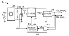
- FIG. 1 is a diagram showing a configuration of a switching power supply device 1 according to an embodiment.
- the switching power supply device 1 is, for example, a power conversion device that converts a commercial AC power supply into a DC power supply, and includes a rectifier circuit 10, a switching (SW) circuit 20, an output circuit 30, and a feedback circuit 40.
- SW switching
- the rectifier circuit 10 is, for example, a diode bridge, which full-wave rectifies the AC Vac output from the commercial AC power supply 5 and outputs the full-wave rectified voltage Vdd to the feeder line 11.
- the voltage Vdd is divided by resistance division or the like and is supplied to the feedback circuit 40 as a signal Vin.
- a smoothing capacitor C is connected in parallel to the output end of the rectifier circuit 10.
- the SW circuit 20 generates a switching voltage Vsw based on the reference signal Vref and the feedback signal Fb output from the feedback circuit 40.
- the output circuit 30 outputs the positive voltage Dc_out (+) and the negative voltage Dc_out (-) from the switching voltage Vsw.
- the output of the switching power supply device 1 is the voltage Dc_out (+) on the positive side and the voltage Dc_out (-) on the negative side, but it may be configured to output only one of the voltages.
- the feedback circuit 40 includes a separator 42 and a feedback signal generation circuit 44.
- the separator 42 outputs, for example, the potential difference between the voltages Dc_out (+) and Dc_out (-) as a signal Vfb via a photocoupler.
- the reason for passing through the photocoupler is to insulate the AC Vac on the input side from the voltages Dc_out (+) and Dc_out (-) on the output side.
- the signal Vfb is a voltage that decreases as the potential difference increases according to the potential difference between the voltages Dc_out (+) and Dc_out (-), and can be rephrased as the negative output voltage of the switching power supply device 1.
- the signal Vfb is a DC voltage corresponding to the voltages Dc_out (+) and Dc_out (-).
- the feedback signal generation circuit 44 is a circuit that outputs a feedback signal Fb to the switching circuit 20 based on the signal Vin input from the rectifier circuit 10 and the signal Vfb output from the separator 42.
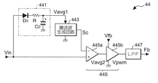
- FIG. 2 is a diagram showing an example of the configuration of the feedback signal generation circuit 44.
- the feedback signal generation circuit 44 includes an averaging circuit 441, a carrier wave generation circuit 443, a PWM circuit 445, and a low-pass filter 447.
- the averaging circuit 441 includes, for example, a diode D0, a resistance element R, and a capacitor C0, and the signal Vin in which the ripple remains is smoothed by the capacitor C0. That is, the averaging circuit 441 outputs the average value of the voltage in the signal Vin.
- the signal output from the averaging circuit 441 is referred to as Vavg1.
- the averaging circuit 441 is a circuit that outputs the signal Vavg1, which is the average value of the signal Vin, to the carrier wave generation circuit 443 based on the signal Vin input from the rectifier circuit 10.
- the average value of the voltage is a value obtained by dividing the integrated value of the voltage in the unit time by the unit time, and in the circuit, it means the voltage appearing at both ends of the capacitor C0.
- the carrier wave generation circuit 443 outputs the carrier wave Sc.
- the waveform of the carrier wave Sc is a triangular wave in which a portion T1 in which the voltage rises and a portion T2 in which the voltage falls in one cycle Tp are repeated.
- the voltage increases non-linearly (non-linearly) with the passage of time, and in the partial T2, the voltage decreases linearly (straight line) with the passage of time.
- the characteristic of the partial T1 is represented by the function F of the following equation (1).
- V F (t ⁇ (1/2)) ... (1) That is, the voltage V in the portion T1 is expressed as a function of time t to the (1/2) power, that is, the square root.
- the non-linear part T1 is the function F in a part of the domain 0 ⁇ t ⁇ 1. It means that it has a shape corresponding to (t ⁇ (1/2)).
- the carrier wave generation circuit 443 makes the wave height Vsow (pp) of the carrier wave Sc proportional to the voltage of the signal Vavg1. Therefore, when the voltage of the signal Vavg1 is a certain value and the carrier wave Sc is output as shown by the solid line A, when the voltage of the signal Vavg1 becomes high, the carrier wave Sc is output as shown by the broken line B1. When the voltage of the signal Vavg1 becomes low, the carrier wave Sc is output as shown by the broken line B2.
- the frequency (1 / Tp) of the carrier wave Sc the frequency of the AC power supply 5 is about several tens of kHz to several hundreds of kHz.
- the wave height is indicated by a peak-to-peak value.
- the carrier wave generation circuit 443 is a circuit that outputs a carrier wave Sc having a wave height proportional to the average value of the signal Vin of the rectifier circuit 10.
- the PWM circuit 445 includes a comparator 445a and a buffer 445b.
- the comparator 445a compares the voltage of the signal Vin with the voltage of the carrier wave Sc, and outputs the signal Vavg2 having a substantially constant wave height as a result of the comparison.
- the comparator 445a outputs the signal Vavg2 at the H level if the voltage of the signal Vin is equal to or higher than the voltage of the carrier Sc, and outputs the signal Vavg2 to L if the voltage of the signal Vin is less than the voltage of the carrier Sc. Output by level.
- the signal Vagv2 is a pulse width modulated signal.
- the buffer 445b is a level shifter, and outputs a signal Vpwm in which the wave height is changed to the signal Vfb while maintaining the pulse shape of the signal Vavg2. That is, the PWM circuit 445 is a circuit that changes the wave height of the signal Vpwm based on the input signal Vfb. Since the signal Vpwm is a signal obtained by level-shifting the signal Vavg2, it is a pulse width-modulated signal similar to the signal Vavg2.
- the low-pass filter 447 demodulates the pulse width-modulated signal Vpwm into the analog voltage feedback signal Fb.
- FIG. 4 is a diagram showing an example of the configuration of the SW circuit 20 and the output circuit 30.
- the SW circuit 20 includes a control circuit 21, drivers 25, 26, switches SwH and SwL, and the output circuit 30 includes a transformer 33 and a rectification smoothing circuit 34.
- the control circuit 21 outputs the signals Sw_H and Sw_L based on the reference signal Vref and the feedback signal Fb.
- the driver 25 amplifies the signal Sw_H and outputs it as a control signal of the switch SwH.
- the driver 26 amplifies the signal Sw_L and outputs it as a control signal of the switch SwL.
- the feeder line 11 to which the voltage Vdd is output is connected to one end of the switch SwH in the SW circuit 20 and one end on the primary side in the transformer 33.
- the other end of the switch SwH is connected to the other end of the primary side of the transformer 33 and one end of the switch SwL.
- the output signal of the driver 25 conducts when the output signal is H level, and is insulated when the output signal is L level.
- the output signal of the driver 26 conducts when the output signal is H level, and is insulated when the output signal is L level.
- a rectifying smoothing circuit 34 is provided on the secondary side of the transformer 33.
- the rectifying smoothing circuit 34 includes diodes D1, D2, capacitors C1 and C2.
- One end of the secondary side of the transformer 33 is connected to the anode of the diode D1, and the cathode of the diode D1 is connected to the output end of the voltage Dc_out (+) and one end of the capacitor C1.
- the other end of the secondary side of the transformer 33 is connected to the cathode of the diode D2, and the anode of the diode D2 is connected to the output end of the voltage Dc_out ( ⁇ ) and one end of the capacitor C2.
- the neutral point on the secondary side of the transformer 33 is connected to the other end of the capacitor C1 and the other end of the capacitor C2, and is isolated from the primary side and grounded.
- the control circuit 21 in the SW circuit 20 controls the duty ratio of the signal Sw_H and the duty ratio of the signal Sw_L so that the difference between the voltage of the reference signal Vref and the voltage of the feedback signal Fb output from the feedback circuit 40 becomes small. ..
- the control circuit 21 controls the duty ratios of the signals Sw_H and Sw_L so that the duty ratio of the voltage Vsw applied to the primary side of the transformer 33 increases as the voltage of the feedback signal Fb increases.
- the signal Vfb is negative, the duty ratio of the voltage Vsw becomes smaller as the output voltage becomes higher, and the duty ratio of the voltage Vsw becomes larger as the output voltage becomes lower. By this operation, the output voltage approaches a predetermined target voltage.
- the factor for reducing the power factor is the means for rectifying and smoothing the AC voltage.
- FIG. 1 it is a rectifier circuit 10 and a capacitor C.
- AC is converted to DC voltage by rectifying and smoothing, and the DC voltage is switched by a switching circuit to stabilize the output voltage. Therefore, the rectifying circuit 10 and the condenser C can be omitted. Can not. Therefore, in the switching power supply device 1 according to the present embodiment, the feedback circuit 40 generates the feedback signal Fb to the SW circuit 20 by the following calculation.
- the voltage of the signal Vin after rectifying and smoothing the AC Vac is squared to generate a signal (Vin ⁇ 2).
- a signal (Vin ⁇ 2 / Vin average value) obtained by dividing the voltage of the signal (Vin ⁇ 2) by the average value of the voltage in the signal Vin is generated.
- the signal ⁇ Vfb ⁇ (Vin ⁇ 2 / Vin average value) ⁇ obtained by multiplying the signal Vfb indicating the output voltage and the signal (Vin ⁇ 2 / Vin average value) is obtained, and the multiplied signal is switched to SW. It is supplied as a feedback signal Fb to the circuit 20.
- the calculation in the feedback circuit 40 includes multiplication and division. Multiplication and division are performed in this embodiment as follows.
- the pulse width modulated signal is a binary signal obtained by comparing the voltage of the input signal Vin with the voltage of the carrier wave.
- the gain G in pulse width modulation can be expressed by the following equation (1).
- G Vout / Vin ... (1)
- Vout is an analog voltage obtained by demodulating the pulse width-modulated signal with a low-pass filter.
- the gain G can also be expressed by the following equation (2).
- G Vpwm (pp) / Vsow (pp)...
- Vpwm (pp) is the voltage wave height in the pulse-modulated signal
- Vsow (pp) is the voltage wave height in the carrier wave as described above. That is, by changing the voltage wave height Vpwm (pp) or / and the voltage wave height Vsow (pp) in the carrier wave in the pulse-modulated signal, the gain G of the pulse width modulation can be changed.
- the gain G is proportional to the wave height Vpwm (pp) and inversely proportional to the wave height Vsow (pp). Therefore, the change in wave height Vpwm (pp) corresponds to multiplication, and the change in wave height Vsow (pp) corresponds to division.
- the inclined portion of the carrier wave is made straight.
- the conversion characteristic of the pulse width modulation is an inverse function of the function F (t). It follows a certain characteristic of F -1 (t). Therefore, when outputting a signal obtained by squaring the voltage of the input signal, this inclined portion is represented by a function F (t ⁇ (1/2)) which is an inverse function of the function F (t ⁇ 2). You just have to do it.
- the inclined portion of the carrier wave is a portion of the carrier wave where a time difference occurs when compared with a different voltage level.
- the pulse width of the signal Vavg2 changes. It is the part that mainly contributes.
- the inclined portion of the carrier wave is a portion excluding the sudden drop (or rapid rise) part of the voltage if it is a sawtooth wave in which the voltage rises and drops (or the voltage drops and suddenly rises) repeatedly with the passage of time. If there is a triangular wave in which the voltage rises and falls alternately, it is the portion where the voltage rises and falls.
- the sudden rise or fall of the voltage in the sawtooth wave is not the sloped part here because the time difference is sufficiently small when compared to different voltage levels.
- the voltage of the feedback signal Fb is the product of the voltage of the signal Vfb and the squared value of the voltage at the signal Vin divided by the average value of the voltage at the signal Vin, that is, ⁇ Vfb ⁇ (Vin ⁇ 2 / Vin average value). ) ⁇ .
- the term (Vin ⁇ 2) is obtained by forming the waveform of the portion T1 on the carrier wave Sc into a shape represented by the function F (t ⁇ (1/2)). ..
- the term (1 / Vin average value) is obtained by changing the wave height of the carrier wave Sc according to the average value of Vin. Therefore, if the signal Vavg2 output from the comparator 445a is demodulated by the low-pass filter, the voltage becomes (Vin ⁇ 2 / Vin average value) as shown in FIG.
- the instantaneous value of (Vin ⁇ 2 / Vin average value) changes according to the instantaneous value of the signal Vin. Further, the wave height and shape of (Vin ⁇ 2 / Vin average value) are almost unchanged when viewed in periodic units. Specifically, the wave height of (Vin ⁇ 2 / Vin average value) is approximately the same regardless of the level of the signal level (average voltage) of the signal Vin, and (Vin ⁇ 2 / Vin average value). In the waveform of, a large value is obtained near the peak in each period of the signal Vin.
- the point to be multiplied by the term of Vfb is achieved by changing the wave height of the signal Vavg2 to the voltage of the signal Vfb by the buffer 445b.
- the feedback signal Fb By demodulating the signal Vpwm in which the wave height of the signal Vavg2 is changed according to the signal Vfb by the low-pass filter 447, the feedback signal Fb having the voltage indicated by the above product is fed back to the SW circuit 20.
- the feedback signal Fb increases near the positive and negative peaks in each cycle of the AC Vac, and the duty ratio of the voltage Vsw increases accordingly. More energy is supplied to the primary side of the transformer 33 near the peak, resulting in an improvement in the power factor of the power supply 1.
- logarithmic transformation utilizes the fact that multiplication can be performed by addition and division by subtraction. and, Input signal ⁇ logarithmic conversion ⁇ addition / subtraction ⁇ inverse logarithmic conversion ⁇ output signal After going through the procedure, multiplication / division becomes possible.
- the absolute value of the voltage Vbe of the transistor is small and the collector current Ic changes greatly with a small change, it is difficult to secure the dynamic range due to the influence of thermal noise or noise of the transistor itself.
- the voltage Vbe is liable to change with temperature, it is necessary to take measures to cancel the influence of temperature, which is a factor of cost increase due to an increase in the number of circuit elements and the use of a dedicated IC.
- the carrier wave Sc is a triangular wave as shown in FIG. 3, but the waveform of the carrier wave Sc may be a sawtooth wave as shown in FIG. That is, in FIG. 3, the portion T2 that decreases with the gradient of the voltage may be eliminated, and only the portion T1 in which the voltage increases in a non-linear manner may be used.
- the non-linear part T1 may have a shape corresponding to the function F (t ⁇ (1/2)) in the entire domain 0 ⁇ t ⁇ 1.
- the portion where the voltage rises in a non-linear manner the slope becomes smaller with the passage of time. For example, as shown in FIG. 6, the higher the voltage of the signal Vin, the more the signal with respect to the change of the voltage of the signal Vin. It suffices if the change in the pulse width of Vavg2 becomes large.
- the portion T1 in which the voltage rises with the passage of time in the carrier wave Sc is defined as non-linear, but the portion T2 in which the voltage decreases with the passage of time in a triangular wave or a sawtooth wave may be defined as non-linear.
- the control circuit 21 a circuit may be used in which the duty ratio of the voltage Vsw applied to the primary side of the transformer 33 becomes smaller as the voltage of the feedback signal Fb becomes larger. In that case, the term of the signal Vfb is positive (value proportional to the output voltage), and the term of (Vin ⁇ 2 / Vin average value) is negative (Vin ⁇ 2 / Vin average value) is reduced from the predetermined value. Value).
- the switching power supply device switches between a rectifying circuit that rectifies an input AC voltage and outputs it as a first voltage and the first voltage based on a feedback signal, and switches signals.
- the feedback circuit includes a switching circuit that generates a second voltage based on the switching voltage, a feedback circuit that generates a feedback signal from the first voltage and the second voltage, and the feedback circuit.
- the circuit is a carrier generation circuit having a predetermined period, the wave height changes according to the average value of the first voltage, and at least one of the rising edge and the falling edge is a nonlinear carrier, and the first voltage.
- a PWM circuit that generates a PWM signal based on a comparison result between the voltage of the carrier and a PWM signal having a wave height corresponding to the second voltage, and a low pass that generates the feedback signal from the PWM signal. Due to the non-linearity of the carrier including the filter, the larger the value of the first voltage, the larger the change in the pulse width of the PWM signal according to the change in the first voltage. According to this aspect, since the operation for generating the feedback signal is executed by pulse width modulation, there are few factors that change with temperature as compared with the configuration using the logarithmic characteristics of the transistor, and the circuit configuration. Is simplified.
- the voltage of the signal Vin is an example of the first voltage
- the voltage Dc_out (+) or Dc_out (-) is an example of the second voltage
- the signal Vpwm is an example of a PWM signal
- the partial T1 is an example of the rising edge of the carrier wave
- the partial T2 is an example of the falling edge of the carrier wave.
- the non-linearity has a shape corresponding to the function F (t ⁇ (1/2)) of the domain 0 ⁇ t ⁇ 1. According to this aspect, it is possible to perform a square calculation when generating a feedback signal.
- the output circuit inputs the switching voltage and outputs the AC voltage, and rectifies and smoothes the AC voltage to obtain the second voltage. Includes a rectifying and smoothing circuit to generate.
- the carrier wave is a sawtooth wave having a non-linear rising or falling edge, or a triangular wave having at least one of a rising edge or a falling edge is non-linear. ..
Landscapes
- Engineering & Computer Science (AREA)
- Power Engineering (AREA)
- Dc-Dc Converters (AREA)
Abstract
力率を改善するスイッチング電源装置1を簡易な構成で実現する。 入力交流電圧を整流して、第1電圧として出力する整流回路10と、第1電圧を、帰還信号Fbに基づいてスイッチングし、スイッチング電圧を生成するSW回路20と、スイッチング電圧から、第2電圧を生成する出力回路30と、第1電圧と第2電圧とから帰還信号Fbを生成する帰還回路40と、を含み、帰還回路40は、所定周期の搬送波であって、第1電圧の平均値に応じて波高が変化し、かつ、立ち上がりと立ち下がり少なくとも一方が非線形の搬送波を生成する搬送波生成回路と、第1電圧と搬送波の電圧との比較結果に基づいたPWM信号であって、かつ、第2電圧に応じた波高を有するPWM信号を生成するPWM回路と、PWM信号から前記帰還信号を生成するローパスフィルターとを含む。
Description
本開示は、スイッチング電源装置に関する。
電子機器等に使用されるスイッチング電源装置は、交流の商用電源を、より高い周波数でスイッチングしなおし、トランスを介して出力して、アイソレートされた直流電源を生成する。スイッチ電源装置では、交流電源を、整流および平滑化し、直流を生成して、スイッチングする。この整流および平滑化においてパルス状の電流が流れると、それによりスイッチング電源装置の力率が悪化する。この電流波形を制御して、力率を改善するため、通常、スイッチング電源装置にはPFC(Power Factor Correction)回路が設けられる(特許文献1参照)。
しかしながら、PFC回路が設けられる構成では、スイッチング電源装置が大規模化する、という問題がある。
上記目的を達成するために、本開示の一態様に係るスイッチング電源装置は、入力交流電圧を整流して、第1電圧として出力する整流回路と、前記第1電圧を、帰還信号に基づいてスイッチングし、スイッチング電圧を生成するスイッチング回路と、前記スイッチング電圧から、第2電圧を生成する出力回路と、前記第1電圧と前記第2電圧とから前記帰還信号を生成する帰還回路と、を含み、前記帰還回路は、所定周期の搬送波であって、前記第1電圧の平均値に応じて波高が変化し、かつ、立ち上がりと立ち下がり少なくとも一方が非線形の搬送波を生成する搬送波生成回路と、前記第1電圧と前記搬送波の電圧との比較結果に基づいたPWM信号であって、かつ、前記第2電圧に応じた波高を有するPWM信号を生成するPWM回路と、前記PWM信号から前記帰還信号を生成するローパスフィルターとを含み、前記搬送波の非線形により、前記PWM信号は、前記第1電圧の値が大きいほど前記第1電圧の変化に応じたパルス幅の変化が大きい。
以下、本開示の実施形態について図面を参照して説明する。
図1は、実施形態に係るスイッチング電源装置1の構成を示す図である。このスイッチング電源装置1は、例えば商用の交流電源を直流電源に変換する電力変換装置であり、整流回路10、スイッチング(SW)回路20、出力回路30および帰還回路40を含む。
図1は、実施形態に係るスイッチング電源装置1の構成を示す図である。このスイッチング電源装置1は、例えば商用の交流電源を直流電源に変換する電力変換装置であり、整流回路10、スイッチング(SW)回路20、出力回路30および帰還回路40を含む。
整流回路10は、例えばダイオードブリッジであり、商用の交流電源5から出力される交流Vacを全波整流して、当該全波整流した電圧Vddを給電線11に出力する。電圧Vddは、抵抗分割等により分圧されて、信号Vinとして帰還回路40に供給される。また、整流回路10の出力端には平滑用のコンデンサーCが並列に接続される。
SW回路20は、基準信号Vrefと帰還回路40から出力される帰還信号Fbとに基づいてスイッチング電圧Vswを生成する。
出力回路30は、スイッチング電圧Vswから、正側の電圧Dc_out(+)および負側のDc_out(-)を出力する。なお、本実施形態では、スイッチング電源装置1の出力を正側の電圧Dc_out(+)および負側のDc_out(-)としているが、どちらか一方の電圧のみを出力する構成としてもよい。
出力回路30は、スイッチング電圧Vswから、正側の電圧Dc_out(+)および負側のDc_out(-)を出力する。なお、本実施形態では、スイッチング電源装置1の出力を正側の電圧Dc_out(+)および負側のDc_out(-)としているが、どちらか一方の電圧のみを出力する構成としてもよい。
帰還回路40は、セパレータ42と帰還信号生成回路44とを含む。セパレータ42は、例えば電圧Dc_out(+)およびDc_out(-)の電位差を、フォトカプラを介して信号Vfbとして出力する。フォトカプラを介するのは、入力側の交流Vacと出力側の電圧Dc_out(+)、Dc_out(-)との絶縁を図るためである。なお、信号Vfbは、電圧Dc_out(+)およびDc_out(-)の電位差に応じて、電位差が大きくなるほど小さくなる電圧であり、スイッチング電源装置1の負極性の出力電圧と言い換えられる。なお、信号Vfbは、電圧Dc_out(+)およびDc_out(-)に応じた直流電圧である。図1に示すように、帰還信号生成回路44は、整流回路10から入力される信号Vinとセパレータ42から出力される信号Vfbに基づいて帰還信号Fbをスイッチング回路20に出力する回路である。
図2は、帰還信号生成回路44の構成の一例を示す図である。帰還信号生成回路44は、平均化回路441、搬送波生成回路443、PWM回路445と、ローパスフィルター447とを含む。
平均化回路441は、例えダイオードD0、抵抗素子RおよびコンデンサーC0を含み、リップルが残存する信号VinをコンデンサーC0によって平滑化する。すなわち、平均化回路441は、信号Vinにおける電圧の平均値を出力する。なお、平均化回路441から出力される信号をVavg1とする。つまり、平均化回路441は、整流回路10から入力される信号Vinに基づいて、信号Vinの平均値である信号Vavg1を搬送波生成回路443に出力する回路である。電圧の平均値とは、単位時間における当該電圧の積分値を当該単位時間で除した値であり、回路でいえば、コンデンサーC0の両端に現れる電圧をいう。
平均化回路441は、例えダイオードD0、抵抗素子RおよびコンデンサーC0を含み、リップルが残存する信号VinをコンデンサーC0によって平滑化する。すなわち、平均化回路441は、信号Vinにおける電圧の平均値を出力する。なお、平均化回路441から出力される信号をVavg1とする。つまり、平均化回路441は、整流回路10から入力される信号Vinに基づいて、信号Vinの平均値である信号Vavg1を搬送波生成回路443に出力する回路である。電圧の平均値とは、単位時間における当該電圧の積分値を当該単位時間で除した値であり、回路でいえば、コンデンサーC0の両端に現れる電圧をいう。
搬送波生成回路443は、搬送波Scを出力する。搬送波Scの波形は、例えば図3に示されるように、1周期Tpにおいて電圧が上昇する部分T1と電圧が低下する部分T2とが繰り返される三角波である。部分T1では電圧が時間経過に対して非線形(非直線)で上昇し、部分T2では時間経過に対して電圧が線形(直線)で低下する。
本実施形態において、部分T1の特性は次式(1)の関数Fで表される。
V=F(t^(1/2))…(1)
すなわち、部分T1における電圧Vは、時間tの(1/2)乗、つまり平方根の関数で示される。
なお、関数Fの時間tについて、搬送波Scの1周期Tpの起点を0とし、終点を1として正規化した場合、非線形の部分T1は、変域0≦t≦1の一部において、関数F(t^(1/2))に対応する形状を有している、ということになる。
本実施形態において、部分T1の特性は次式(1)の関数Fで表される。
V=F(t^(1/2))…(1)
すなわち、部分T1における電圧Vは、時間tの(1/2)乗、つまり平方根の関数で示される。
なお、関数Fの時間tについて、搬送波Scの1周期Tpの起点を0とし、終点を1として正規化した場合、非線形の部分T1は、変域0≦t≦1の一部において、関数F(t^(1/2))に対応する形状を有している、ということになる。
また、搬送波生成回路443は、搬送波Scの波高Vsow(p-p)を、信号Vavg1の電圧に比例させる。このため、信号Vavg1の電圧がある値の場合に、搬送波Scが実線Aのように出力される状況において、信号Vavg1の電圧が高くなった場合には、搬送波Scが破線B1のように出力され、信号Vavg1の電圧が低くなった場合には、搬送波Scが破線B2のように出力される。
なお、搬送波Scの周波数(1/Tp)は、交流電源5の周波数は数十kHz~数百kHz程度である。また、波高はピークトゥピーク値で示される。
このような搬送波生成回路443は、例えば、搬送波Scの基本波形をメモリに記憶させておき、当該メモリから波形を繰り返して読み出すとともに、その波高Vsow(p-p)を、信号Vavg1の電圧に比例させて出力する構成により実現できる。また、搬送波生成回路443は、整流回路10の信号Vinの平均値に比例する波高を有する搬送波Scを出力する回路であるということもできる。
なお、搬送波Scの周波数(1/Tp)は、交流電源5の周波数は数十kHz~数百kHz程度である。また、波高はピークトゥピーク値で示される。
このような搬送波生成回路443は、例えば、搬送波Scの基本波形をメモリに記憶させておき、当該メモリから波形を繰り返して読み出すとともに、その波高Vsow(p-p)を、信号Vavg1の電圧に比例させて出力する構成により実現できる。また、搬送波生成回路443は、整流回路10の信号Vinの平均値に比例する波高を有する搬送波Scを出力する回路であるということもできる。
PWM回路445は、コンパレーター445aとバッファ445bとを含む。
コンパレーター445aにおいて、正入力端(+)には信号Vinが供給され、負入力端(-)には搬送波Scが供給される。このため、コンパレーター445aは、信号Vinの電圧と搬送波Scの電圧とを比較し、当該比較の結果として、波高がほぼ一定の信号Vavg2を出力する。詳細には、コンパレーター445aは、信号Vinの電圧が搬送波Scの電圧以上であれば、信号Vavg2をHレベルで出力し、信号Vinの電圧が搬送波Scの電圧未満であれば、信号Vavg2をLレベルで出力する。信号Vagv2は、パルス幅変調された信号である。バッファ445bはレベルシフタであって、信号Vavg2のパルス形状を保ったまま、その波高を信号Vfbに変えた信号Vpwmを出力する。すなわち、PWM回路445は、入力された信号Vfbに基づいて、信号Vpwmの波高を変更する回路である。なお、信号Vpwmは、信号Vavg2をレベルシフトした信号であるので、信号Vavg2と同様にパルス幅変調された信号である。
コンパレーター445aにおいて、正入力端(+)には信号Vinが供給され、負入力端(-)には搬送波Scが供給される。このため、コンパレーター445aは、信号Vinの電圧と搬送波Scの電圧とを比較し、当該比較の結果として、波高がほぼ一定の信号Vavg2を出力する。詳細には、コンパレーター445aは、信号Vinの電圧が搬送波Scの電圧以上であれば、信号Vavg2をHレベルで出力し、信号Vinの電圧が搬送波Scの電圧未満であれば、信号Vavg2をLレベルで出力する。信号Vagv2は、パルス幅変調された信号である。バッファ445bはレベルシフタであって、信号Vavg2のパルス形状を保ったまま、その波高を信号Vfbに変えた信号Vpwmを出力する。すなわち、PWM回路445は、入力された信号Vfbに基づいて、信号Vpwmの波高を変更する回路である。なお、信号Vpwmは、信号Vavg2をレベルシフトした信号であるので、信号Vavg2と同様にパルス幅変調された信号である。
ローパスフィルター447は、パルス幅変調された信号Vpwmをアナログ電圧の帰還信号Fbに復調する。
図4は、SW回路20および出力回路30の構成の一例を示す図である。SW回路20は、制御回路21、ドライバー25、26、スイッチSwHおよびSwLを含み、出力回路30は、トランス33および整流平滑化回路34を含む。
制御回路21は、基準信号Vrefと帰還信号Fbとに基づいて信号Sw_HおよびSw_Lを出力する。
ドライバー25は、信号Sw_Hを増幅し、スイッチSwHの制御信号として出力する。ドライバー26は、信号Sw_Lを増幅して、スイッチSwLの制御信号として出力する。電圧Vddが出力される給電線11は、SW回路20におけるスイッチSwHの一端およびトランス33における一次側の一端に接続される。スイッチSwHの他端は、トランス33における一次側の他端およびスイッチSwLの一端に接続される。
スイッチSwHにおける一端および他端の間は、ドライバー25の出力信号がHレベルのときに導通し、当該出力信号がLレベルのときに絶縁する。同様に、スイッチSwLにおける一端および他端の間は、ドライバー26の出力信号がHレベルのときに導通し、当該出力信号がLレベルのときに絶縁する。
ドライバー25は、信号Sw_Hを増幅し、スイッチSwHの制御信号として出力する。ドライバー26は、信号Sw_Lを増幅して、スイッチSwLの制御信号として出力する。電圧Vddが出力される給電線11は、SW回路20におけるスイッチSwHの一端およびトランス33における一次側の一端に接続される。スイッチSwHの他端は、トランス33における一次側の他端およびスイッチSwLの一端に接続される。
スイッチSwHにおける一端および他端の間は、ドライバー25の出力信号がHレベルのときに導通し、当該出力信号がLレベルのときに絶縁する。同様に、スイッチSwLにおける一端および他端の間は、ドライバー26の出力信号がHレベルのときに導通し、当該出力信号がLレベルのときに絶縁する。
トランス33の二次側には、整流平滑化回路34が設けられる。詳細には、整流平滑化回路34は、ダイオードD1、D2、コンデンサーC1およびC2を含む。トランス33における二次側の一端は、ダイオードD1のアノードに接続され、ダイオードD1のカソードは、電圧Dc_out(+)の出力端およびコンデンサーC1の一端に接続される。トランス33における二次側の他端は、ダイオードD2のカソードに接続され、ダイオードD2のアノードは、電圧Dc_out(-)の出力端およびコンデンサーC2の一端に接続される。トランス33における二次側の中性点は、コンデンサーC1の他端およびコンデンサーC2の他端に接続されて、一次側とは絶縁されて接地される。
SW回路20における制御回路21は、基準信号Vrefの電圧と帰還回路40から出力される帰還信号Fbの電圧との差が小さくなるように、信号Sw_Hのデューティー比および信号Sw_Lのデューティー比を制御する。制御回路21は、帰還信号Fbの電圧が大きくなるほど、トランス33の一次側に掛かる電圧Vswのデューティ比が大きくなるよう、信号Sw_H及び信号Sw_Lのデューティ比を制御する。先述したように、信号Vfbは負極性であるので、出力電圧が高くなるほど電圧Vswのデューティ比は小さくなり、出力電圧が低くなるほど電圧Vswのデューティ比は大きくなる。この動作により、出力電圧は、所定の目標電圧に近づく。
一般的なスイッチング電源装置において、具体的には出力信号の電圧がSW回路20に直接帰還される構成において、力率を低下させる要因は、交流電圧を整流および平滑化する手段にある。具体的には、図1でいえば整流回路10およびコンデンサーCである。スイッチング電源装置では、交流を整流および平滑化することで直流電圧に変換し、当該直流電圧をスイッチング回路によりスイッチングすることで出力電圧を安定化させるので、整流回路10およびコンデンサーCを省略することができない。
そこで、本実施形態に係るスイッチング電源装置1では、帰還回路40が、SW回路20への帰還信号Fbを次のような演算により生成している。
第1に、交流Vacを整流および平滑化した後の信号Vinの電圧を、二乗した信号(Vin^2)を生成する。
第2に、交流Vac(信号Vin)の電圧変動を吸収するために、信号(Vin^2)の電圧を信号Vinにおける電圧の平均値で除した信号(Vin^2/Vin平均値)を生成する。
第3に、出力電圧を示す信号Vfbと、信号(Vin^2/Vin平均値)とを乗算した信号{Vfb×(Vin^2/Vin平均値)}を求めて、当該乗算した信号をSW回路20への帰還信号Fbとして供給する。
そこで、本実施形態に係るスイッチング電源装置1では、帰還回路40が、SW回路20への帰還信号Fbを次のような演算により生成している。
第1に、交流Vacを整流および平滑化した後の信号Vinの電圧を、二乗した信号(Vin^2)を生成する。
第2に、交流Vac(信号Vin)の電圧変動を吸収するために、信号(Vin^2)の電圧を信号Vinにおける電圧の平均値で除した信号(Vin^2/Vin平均値)を生成する。
第3に、出力電圧を示す信号Vfbと、信号(Vin^2/Vin平均値)とを乗算した信号{Vfb×(Vin^2/Vin平均値)}を求めて、当該乗算した信号をSW回路20への帰還信号Fbとして供給する。
このように帰還回路40での演算には、乗算および除算が含まれる。乗算および除算は、本実施形態では、次のようにして実行される。
パルス幅変調された信号は、入力信号Vinの電圧と搬送波の電圧とを比較して得られる二値信号である。パルス幅変調におけるゲインGは、次式(1)のように表すことできる。
G=Vout/Vin …(1)
式(1)において、Voutは、パルス幅変調された信号をローパスフィルターで復調することで得られるアナログ電圧である。
G=Vout/Vin …(1)
式(1)において、Voutは、パルス幅変調された信号をローパスフィルターで復調することで得られるアナログ電圧である。
また、ゲインGは、次式(2)のように表すこともできる。
G=Vpwm(p-p)/Vsow(p-p) …(2)
式(2)において、Vpwm(p-p)はパルス変調された信号における電圧の波高であり、Vsow(p-p)は上述したように搬送波における電圧の波高である。
つまり、パルス変調された信号における電圧の波高Vpwm(p-p)、または/および、搬送波における電圧の波高Vsow(p-p)を変化させると、パルス幅変調のゲインGを変化させることができる。
式(2)から判るように、ゲインGは、波高Vpwm(p-p)に比例し、波高Vsow(p-p)に反比例する。このため、波高Vpwm(p-p)の変化は乗算に相当し、波高Vsow(p-p)の変化は除算に相当する。
G=Vpwm(p-p)/Vsow(p-p) …(2)
式(2)において、Vpwm(p-p)はパルス変調された信号における電圧の波高であり、Vsow(p-p)は上述したように搬送波における電圧の波高である。
つまり、パルス変調された信号における電圧の波高Vpwm(p-p)、または/および、搬送波における電圧の波高Vsow(p-p)を変化させると、パルス幅変調のゲインGを変化させることができる。
式(2)から判るように、ゲインGは、波高Vpwm(p-p)に比例し、波高Vsow(p-p)に反比例する。このため、波高Vpwm(p-p)の変化は乗算に相当し、波高Vsow(p-p)の変化は除算に相当する。
パルス幅変調において、入力信号から出力信号(すなわち、パルス幅変調された信号をローパスフィルターで搬送波成分を除去した復調信号)への変換特性をリニアにするためには、搬送波の傾斜部分を直線にする必要がある。
逆にいえば、傾斜部分が直線ではなく、例えば、時間tで変化する関数F(t)にしたがって湾曲していると、パルス幅変調の変換特性は、当該関数F(t)の逆関数であるF-1(t)の特性にしたがうことになる。
このため、入力信号の電圧を二乗した信号を出力する場合、この傾斜部分を、関数F(t^2)の逆関数である関数F(t^(1/2))で表される形状とすればよいことになる。
逆にいえば、傾斜部分が直線ではなく、例えば、時間tで変化する関数F(t)にしたがって湾曲していると、パルス幅変調の変換特性は、当該関数F(t)の逆関数であるF-1(t)の特性にしたがうことになる。
このため、入力信号の電圧を二乗した信号を出力する場合、この傾斜部分を、関数F(t^2)の逆関数である関数F(t^(1/2))で表される形状とすればよいことになる。
なお、搬送波の傾斜部分とは、搬送波のうち、異なる電圧レベルと比較したときに時間差が生じる部分であり、換言すれば、信号Vinの電圧が変化したときに、信号Vavg2のパルス幅の変化に主に寄与する部分である。具体的には、搬送波の傾斜部分とは、時間経過とともに電圧の上昇および急降下(または電圧の下降および急上昇)が繰り返される鋸波であれば、電圧の急降下(または急上昇)部分を除いた部分であり、電圧の上昇および下降が交互に繰り返される三角波であれば、その電圧の上昇および下降する部分である。鋸波における電圧の急上昇部分または急降下部分では、異なる電圧レベルと比較したときに時間差が十分に小さいので、ここでいう傾斜部分ではない。
帰還信号Fbの電圧は、信号Vfbの電圧と、信号Vinにおける電圧の二乗値を当該信号Vinにおける電圧の平均値で除した値と、の積、すなわち{Vfb×(Vin^2/Vin平均値)}である。
本実施形態では、上記積のうち、(Vin^2)の項については、搬送波Scにおける部分T1の波形を関数F(t^(1/2))で表される形状とすることで求められる。(1/Vin平均値)の項については、搬送波Scの波高をVinの平均値に応じて変化させることで求められる。このため、コンパレーター445aから出力される信号Vavg2は、仮にローパスフィルターで復調されると、図5に示されるように、(Vin^2/Vin平均値)の電圧となる。
本実施形態では、上記積のうち、(Vin^2)の項については、搬送波Scにおける部分T1の波形を関数F(t^(1/2))で表される形状とすることで求められる。(1/Vin平均値)の項については、搬送波Scの波高をVinの平均値に応じて変化させることで求められる。このため、コンパレーター445aから出力される信号Vavg2は、仮にローパスフィルターで復調されると、図5に示されるように、(Vin^2/Vin平均値)の電圧となる。
なお、(Vin^2/Vin平均値)の瞬時値は、信号Vinの瞬時値に応じて変化する。また、(Vin^2/Vin平均値)の波高および形状とは、周期単位でみれば、ほぼ変化しない。具体的には、(Vin^2/Vin平均値)の波高については、信号Vinの信号レベル(平均電圧)の高低にかかわらず、おおよそ同じであり、かつ、(Vin^2/Vin平均値)の波形では、信号Vinの各周期におけるピーク付近で大きな値となる。
次に、上記積のうち、Vfbの項を乗じる点については、信号Vavg2の波高を、バッファ445bによって信号Vfbの電圧に変えることにより達成される。
信号Vavg2の波高を信号Vfbに応じて変えた信号Vpwmを、ローパスフィルター447で復調することにより、上記積で示される電圧を有する帰還信号FbがSW回路20に帰還される。帰還信号Fbは交流Vacの各周期における正と負のピーク付近で大きくなり、それに応じて電圧Vswのデューティ比も大きくなる。ピーク付近でトランス33の一次側により多くのエネルギーが供給され、結果として電源装置1の力率が改善される。
次に、上記積のうち、Vfbの項を乗じる点については、信号Vavg2の波高を、バッファ445bによって信号Vfbの電圧に変えることにより達成される。
信号Vavg2の波高を信号Vfbに応じて変えた信号Vpwmを、ローパスフィルター447で復調することにより、上記積で示される電圧を有する帰還信号FbがSW回路20に帰還される。帰還信号Fbは交流Vacの各周期における正と負のピーク付近で大きくなり、それに応じて電圧Vswのデューティ比も大きくなる。ピーク付近でトランス33の一次側により多くのエネルギーが供給され、結果として電源装置1の力率が改善される。
従来において乗算および除算をアナログ演算で実行する場合には、トランジスターのベース・エミッタ間の電圧Vbeとコレクタ電流Icとの対数特性が用いられることが多い。具体的には、対数変換(log変換)すると、乗算が加算で、除算が減算で行えることを利用する。そして、
入力信号→対数変換→加算/減算→逆対数変換→出力信号
という手順を経ると、乗算/除算が可能になる。
しかしながら、トランジスターの電圧Vbeの絶対値が小さく、微小な変化でコレクタ電流Icが大きく変化するので、トランジスター自身の熱雑音やノイズの影響でダイナミックレンジを確保することが難しい。また、電圧Vbeが温度で変化しやすいので、温度の影響をキャンセルする工夫が必要となり、回路素子数の増加や専用IC化などのためにコストアップの要因になっている。
入力信号→対数変換→加算/減算→逆対数変換→出力信号
という手順を経ると、乗算/除算が可能になる。
しかしながら、トランジスターの電圧Vbeの絶対値が小さく、微小な変化でコレクタ電流Icが大きく変化するので、トランジスター自身の熱雑音やノイズの影響でダイナミックレンジを確保することが難しい。また、電圧Vbeが温度で変化しやすいので、温度の影響をキャンセルする工夫が必要となり、回路素子数の増加や専用IC化などのためにコストアップの要因になっている。
これに対して、本実施形態では、二乗を含む乗算および除算の演算がパルス幅変調により実現されるので、上記トランジスターの対数特性を用いた構成と比較して、温度で変化する要素が少なく、また、回路構成の簡易化が図られる。
上述した実施形態では、搬送波Scを図3に示されるような三角波としたが、搬送波Scの波形としては、図6に示されるような鋸波としてもよい。すなわち、図3において電圧の傾斜を伴って低下する部分T2をなくして、非線形で電圧が上昇する部分T1のみとしてもよい。換言すれば、非線形の部分T1は、変域0≦t≦1の全部において、関数F(t^(1/2))に対応する形状を有してもよい。
なお、電圧が非線形で上昇する部分については、時間経過とともに傾きが小さくなって、例えば図6に示されるように、信号Vinの電圧が高いほど、当該信号Vinの電圧の変化に対して、信号Vavg2のパルス幅の変化が大きくなればよい。
なお、電圧が非線形で上昇する部分については、時間経過とともに傾きが小さくなって、例えば図6に示されるように、信号Vinの電圧が高いほど、当該信号Vinの電圧の変化に対して、信号Vavg2のパルス幅の変化が大きくなればよい。
また、図3または図6においては、搬送波Scにおいて電圧が時間経過とともに上昇する部分T1を非線形としたが、三角波または鋸波において電圧が時間経過とともに低下する部分T2を非線形としてもよい。制御回路21として、帰還信号Fbの電圧が大きくなるほど、トランス33の一次側に掛かる電圧Vswのデューティ比を小さくする回路を用いても良い。その場合、信号Vfbの項を正極性(出力電圧に比例する値)とし、(Vin^2/Vin平均値)の項を負極性(所定値から(Vin^2/Vin平均値)を減産した値)とすればよい。
<付記>
上述した実施形態等から、例えば以下のような態様が把握される。
上述した実施形態等から、例えば以下のような態様が把握される。
本開示の態様(第1態様)に係るスイッチング電源装置は、入力交流電圧を整流して、第1電圧として出力する整流回路と、前記第1電圧を、帰還信号に基づいてスイッチングし、スイッチング信号を生成するスイッチング回路と、前記スイッチング電圧に基づいて、第2電圧を生成する出力回路と、前記第1電圧と前記第2電圧とから前記帰還信号を生成する帰還回路と、を含み、前記帰還回路は、所定周期の搬送波であって、前記第1電圧の平均値に応じて波高が変化し、かつ、立ち上がりと立ち下がり少なくとも一方が非線形の搬送波を生成する搬送波生成回路と、前記第1電圧と前記搬送波の電圧との比較結果に基づいたPWM信号であって、かつ、前記第2電圧に応じた波高を有するPWM信号を生成するPWM回路と、前記PWM信号から前記帰還信号を生成するローパスフィルターとを含み、前記搬送波の非線形により、前記PWM信号は、前記第1電圧の値が大きいほど前記第1電圧の変化に応じたパルス幅の変化が大きい。
この態様によれば、帰還信号を生成するに際の演算がパルス幅変調により実行されるので、トランジスターの対数特性を用いた構成と比較して、温度で変化する要素が少なく、また、回路構成の簡易化が図られる。
なお、信号Vinの電圧が第1電圧の一例であり、電圧Dc_out(+)またはDc_out(-)が第2電圧の一例である。また、信号VpwmがPWM信号の一例である。また、部分T1が搬送波の立ち上がりの一例であり、部分T2が搬送波の立ち下がりの一例である。
この態様によれば、帰還信号を生成するに際の演算がパルス幅変調により実行されるので、トランジスターの対数特性を用いた構成と比較して、温度で変化する要素が少なく、また、回路構成の簡易化が図られる。
なお、信号Vinの電圧が第1電圧の一例であり、電圧Dc_out(+)またはDc_out(-)が第2電圧の一例である。また、信号VpwmがPWM信号の一例である。また、部分T1が搬送波の立ち上がりの一例であり、部分T2が搬送波の立ち下がりの一例である。
第1態様の例(第2態様)において、前記非線形は、変域0≦t≦1の関数F(t^(1/2))に対応する形状を有する。この態様によれば、帰還信号を生成する際の二乗の演算を実行することができる。
第1または第2態様の例(第3態様)において、前記出力回路は、前記スイッチング電圧を入力して、交流電圧を出力するトランスと、前記交流電圧を整流平滑化して、前記第2電圧を生成する整流平滑化回路と、を含む。
第1乃至第3のいずれかの態様の例(第4態様)において、前記搬送波は、立ち上がりまたは立ち下がりが非線形である鋸波、もしくは、少なくとも立ち上がりまたは立ち下がりの一方が非線形である三角波である。
第1乃至第3のいずれかの態様の例(第4態様)において、前記搬送波は、立ち上がりまたは立ち下がりが非線形である鋸波、もしくは、少なくとも立ち上がりまたは立ち下がりの一方が非線形である三角波である。
1…スイッチング電源装置、10…整流回路、20…スイッチング回路、30…出力回路、33…トランス、34…整流平滑化回路、40…帰還回路、44…帰還信号生成回路、443…搬送波生成回路、445…PWM回路、447…ローパスフィルター。
Claims (10)
- 入力交流電圧を整流して、第1電圧として出力する整流回路と、
前記第1電圧を、帰還信号に基づいてスイッチングし、スイッチング電圧を生成するスイッチング回路と、
前記スイッチング電圧から、第2電圧を生成する出力回路と、
前記第1電圧と前記第2電圧とから前記帰還信号を生成する帰還回路と、を含み、
前記帰還回路は、
所定周期の搬送波であって、前記第1電圧の平均値に応じて波高が変化し、かつ、立ち上がりと立ち下がり少なくとも一方が非線形の搬送波を生成する搬送波生成回路と、
前記第1電圧と前記搬送波の電圧との比較結果に基づいたPWM信号であって、かつ、前記第2電圧に応じた波高を有するPWM信号を生成するPWM回路と、
前記PWM信号から前記帰還信号を生成するローパスフィルターと、を含み、
前記搬送波の非線形により、前記PWM信号は、前記第1電圧の値が大きいほど前記第1電圧の変化に応じたパルス幅の変化が大きい、スイッチング電源装置。 - 前記非線形は、変域0≦t≦1の関数F(t^(1/2))に対応する形状を有する請求項1のスイッチング電源装置。
- 前記出力回路は、
前記スイッチング電圧)が入力され、交流電圧を出力するトランスと、
前記交流電圧を整流平滑化して、前記第2電圧を生成する整流平滑化回路と、を含む請求項1または2のスイッチング電源装置。 - 前記搬送波は、立ち上がりまたは立ち下がりが非線形である鋸波、もしくは、少なくとも立ち上がりまたは立ち下がりの一方が非線形である三角波である請求項1乃至3のいずれかのスイッチング電源装置。
- 前記帰還回路は、
前記整流回路から前記第1電圧が入力される帰還信号生成回路と、
前記出力回路から前記第2電圧が入力されるセパレータと、を含み、
前記帰還信号生成回路は、入力された前記第1電圧及び前記セパレータからの出力に基づいて前記帰還信号を前記スイッチング回路に出力する請求項1乃至4のいずれかのスイッチング電源装置。 - 前記帰還回路は、入力された前記第1電圧に基づいて前記第1電圧の平均値を前記搬送波出力回路に出力する平均化回路を、さらに備える請求項1乃至5のいずれかのスイッチング電源装置。
- 前記搬送波出力回路から出力される前記搬送波の波高は、入力される前記第1電圧の平均値に比例する請求項1乃至6のいずれかのスイッチング電源装置。
- 前記出力回路は、入力された前記スイッチング電圧に基づいて前記第2電圧の正側の電圧及び負側の電圧を出力するものであり、
前記帰還回路の前記PWM回路には、前記第2電圧の前記正側の電圧と前記負側の電圧の電位差に応じた電位差電圧が入力される請求項1乃至7のいずれかのスイッチング電源装置。 - 前記PWM回路は、入力された前記電位差電圧に基づいて、前記PWM信号の波高を変更する請求項8のスイッチング電源装置。
- 前記PWM回路から出力される信号は、前記電位差電圧と前記第1電圧の2乗の積を前記第1電圧の平均値で除算したものである請求項9のスイッチング電源装置。
Priority Applications (2)
| Application Number | Priority Date | Filing Date | Title |
|---|---|---|---|
| JP2022546310A JP7392864B2 (ja) | 2020-09-02 | 2021-08-30 | スイッチング電源装置 |
| US18/116,021 US12261523B2 (en) | 2020-09-02 | 2023-03-01 | Switching power supply |
Applications Claiming Priority (2)
| Application Number | Priority Date | Filing Date | Title |
|---|---|---|---|
| JP2020147424 | 2020-09-02 | ||
| JP2020-147424 | 2020-09-02 |
Related Child Applications (1)
| Application Number | Title | Priority Date | Filing Date |
|---|---|---|---|
| US18/116,021 Continuation US12261523B2 (en) | 2020-09-02 | 2023-03-01 | Switching power supply |
Publications (1)
| Publication Number | Publication Date |
|---|---|
| WO2022050226A1 true WO2022050226A1 (ja) | 2022-03-10 |
Family
ID=80491722
Family Applications (1)
| Application Number | Title | Priority Date | Filing Date |
|---|---|---|---|
| PCT/JP2021/031760 Ceased WO2022050226A1 (ja) | 2020-09-02 | 2021-08-30 | スイッチング電源装置 |
Country Status (3)
| Country | Link |
|---|---|
| US (1) | US12261523B2 (ja) |
| JP (1) | JP7392864B2 (ja) |
| WO (1) | WO2022050226A1 (ja) |
Citations (5)
| Publication number | Priority date | Publication date | Assignee | Title |
|---|---|---|---|---|
| JPH05300734A (ja) * | 1992-04-18 | 1993-11-12 | Nippon Purotekutaa:Kk | スイッチングレギュレータ |
| JPH0622546A (ja) * | 1992-07-03 | 1994-01-28 | Nippon Purotekutaa:Kk | スイッチングレギュレータ |
| JP2010124567A (ja) * | 2008-11-18 | 2010-06-03 | Nayuta:Kk | スイッチング電源装置 |
| JP2012191775A (ja) * | 2011-03-11 | 2012-10-04 | Eye Lighting Syst Corp | 直流電源装置、および、これを備えたled照明器具 |
| JP2020137322A (ja) * | 2019-02-22 | 2020-08-31 | Ntn株式会社 | スイッチング電源用pwm制御装置 |
Family Cites Families (5)
| Publication number | Priority date | Publication date | Assignee | Title |
|---|---|---|---|---|
| US5867379A (en) * | 1995-01-12 | 1999-02-02 | University Of Colorado | Non-linear carrier controllers for high power factor rectification |
| US5804950A (en) * | 1996-06-20 | 1998-09-08 | Micro Linear Corporation | Input current modulation for power factor correction |
| US5689176A (en) * | 1996-08-07 | 1997-11-18 | Deloy; Jeff J. | Power factor/harmonics correction circuitry and method thereof |
| US8004262B2 (en) * | 2008-11-07 | 2011-08-23 | Power Integrations, Inc. | Method and apparatus to control a power factor correction circuit |
| JP5400833B2 (ja) | 2011-06-06 | 2014-01-29 | シャープ株式会社 | スイッチング電源回路、半導体装置、led照明装置 |
-
2021
- 2021-08-30 WO PCT/JP2021/031760 patent/WO2022050226A1/ja not_active Ceased
- 2021-08-30 JP JP2022546310A patent/JP7392864B2/ja active Active
-
2023
- 2023-03-01 US US18/116,021 patent/US12261523B2/en active Active
Patent Citations (5)
| Publication number | Priority date | Publication date | Assignee | Title |
|---|---|---|---|---|
| JPH05300734A (ja) * | 1992-04-18 | 1993-11-12 | Nippon Purotekutaa:Kk | スイッチングレギュレータ |
| JPH0622546A (ja) * | 1992-07-03 | 1994-01-28 | Nippon Purotekutaa:Kk | スイッチングレギュレータ |
| JP2010124567A (ja) * | 2008-11-18 | 2010-06-03 | Nayuta:Kk | スイッチング電源装置 |
| JP2012191775A (ja) * | 2011-03-11 | 2012-10-04 | Eye Lighting Syst Corp | 直流電源装置、および、これを備えたled照明器具 |
| JP2020137322A (ja) * | 2019-02-22 | 2020-08-31 | Ntn株式会社 | スイッチング電源用pwm制御装置 |
Also Published As
| Publication number | Publication date |
|---|---|
| US12261523B2 (en) | 2025-03-25 |
| US20230208311A1 (en) | 2023-06-29 |
| JP7392864B2 (ja) | 2023-12-06 |
| JPWO2022050226A1 (ja) | 2022-03-10 |
Similar Documents
| Publication | Publication Date | Title |
|---|---|---|
| JP5170096B2 (ja) | Pfcコンバータ | |
| EP1229634B1 (en) | Switching power supply apparatus | |
| US9491819B2 (en) | Hysteretic power factor control method for single stage power converters | |
| JP6272691B2 (ja) | 振幅正規化回路、電源装置および電子機器 | |
| TWI491154B (zh) | 交直流轉換電源供應裝置及其電源控制架構與方法 | |
| KR100221705B1 (ko) | 교류.직류 변환용 전원 회로 | |
| US8787039B2 (en) | Hybrid adaptive power factor correction schemes for switching power converters | |
| JP5400833B2 (ja) | スイッチング電源回路、半導体装置、led照明装置 | |
| JP6481516B2 (ja) | スイッチング電源のスイッチング制御装置 | |
| US8907648B2 (en) | Power factor correction circuit, control circuit therefor and method for driving load circuit through power factor correction | |
| US20130223119A1 (en) | Boost pfc controller | |
| US20130038229A1 (en) | Light-emitting device control circuit | |
| US11601043B2 (en) | Control method and control circuit for an AC-DC power supply | |
| WO2010109694A1 (ja) | スイッチング電源装置 | |
| JP4104868B2 (ja) | スイッチング電源装置 | |
| US20050219871A1 (en) | Piecewise on-time modulation apparatus and method for a power factor corrector | |
| US7199561B2 (en) | DC-DC converter and converter device | |
| US12476536B2 (en) | Multi-mode PFC circuit and control method thereof | |
| US7352599B2 (en) | Switching power source apparatus | |
| US20240275273A1 (en) | Multi-mode pfc circuit and control method thereof | |
| JP7392864B2 (ja) | スイッチング電源装置 | |
| JP4423994B2 (ja) | 力率改善回路 | |
| JP2001320880A (ja) | 整流電源 | |
| JP2968670B2 (ja) | 保護回路付きdc−dcコンバータ | |
| US12095359B2 (en) | Power factor correction converter, controller and digital peak-hold circuit thereof |
Legal Events
| Date | Code | Title | Description |
|---|---|---|---|
| 121 | Ep: the epo has been informed by wipo that ep was designated in this application |
Ref document number: 21864284 Country of ref document: EP Kind code of ref document: A1 |
|
| ENP | Entry into the national phase |
Ref document number: 2022546310 Country of ref document: JP Kind code of ref document: A |
|
| NENP | Non-entry into the national phase |
Ref country code: DE |
|
| 122 | Ep: pct application non-entry in european phase |
Ref document number: 21864284 Country of ref document: EP Kind code of ref document: A1 |