WO2022049999A1 - 半導体装置 - Google Patents
半導体装置 Download PDFInfo
- Publication number
- WO2022049999A1 WO2022049999A1 PCT/JP2021/029378 JP2021029378W WO2022049999A1 WO 2022049999 A1 WO2022049999 A1 WO 2022049999A1 JP 2021029378 W JP2021029378 W JP 2021029378W WO 2022049999 A1 WO2022049999 A1 WO 2022049999A1
- Authority
- WO
- WIPO (PCT)
- Prior art keywords
- metal plate
- electrode pad
- semiconductor device
- transistor chip
- wire
- Prior art date
- Legal status (The legal status is an assumption and is not a legal conclusion. Google has not performed a legal analysis and makes no representation as to the accuracy of the status listed.)
- Ceased
Links
Images



Classifications
-
- H—ELECTRICITY
- H10—SEMICONDUCTOR DEVICES; ELECTRIC SOLID-STATE DEVICES NOT OTHERWISE PROVIDED FOR
- H10W—GENERIC PACKAGES, INTERCONNECTIONS, CONNECTORS OR OTHER CONSTRUCTIONAL DETAILS OF DEVICES COVERED BY CLASS H10
- H10W72/00—Interconnections or connectors in packages
Definitions
- This disclosure relates to semiconductor devices.
- Patent Document 1 Packaged semiconductor devices are known (see, for example, Patent Document 1).
- the semiconductor device disclosed in Patent Document 1 has two power device dies facing each other.
- the semiconductor device includes a drain terminal, a source terminal, and a gate terminal.
- the semiconductor device includes a first metal plate, a second metal plate arranged at intervals from the first metal plate, and a third metal arranged at intervals from each of the first metal plate and the second metal plate.
- the SiC transistor chip is provided with a second SiC transistor chip which is plate-shaped and is mounted on a first metal plate adjacent to the first SiC transistor chip.
- the first metal plate and the drain terminal are electrically connected.
- the second metal plate and the source terminal are electrically connected.
- the third metal plate and the gate terminal are electrically connected.
- the first SiC transistor chip includes a first source electrode pad and a first gate electrode pad arranged on one side in the thickness direction, and a first drain electrode pad arranged on the other side in the thickness direction.
- the second SiC transistor chip includes a second source electrode pad and a second gate electrode pad arranged on one side in the thickness direction, and a second drain electrode pad arranged on the other side in the thickness direction. ,including.
- the first drain electrode pad is joined to the first metal plate.
- the second drain electrode pad is joined to the first metal plate.
- the semiconductor device includes a first conductor that electrically connects each of the first source electrode pad and the second source electrode pad and the second metal plate, and the first gate electrode pad and the second gate electrode pad.
- a second conductor that electrically connects each to the third metal plate, and one first wire that electrically connects the first source electrode pad, the second source electrode pad, and the fourth metal plate. To prepare for. At least one end of the first wire is joined
- FIG. 1 is a schematic plan view of the semiconductor device according to the first embodiment.
- FIG. 2 is a schematic plan view showing a part of the semiconductor device shown in FIG. 1 in an enlarged manner.
- FIG. 3 is a schematic cross-sectional view showing a part of the semiconductor device shown in FIG. 1 in an enlarged manner.
- FIG. 4 is a schematic plan view showing an enlarged part of the semiconductor device according to the second embodiment.
- FIG. 5 is a schematic plan view showing an enlarged part of the semiconductor device according to the third embodiment.
- FIG. 6 is a schematic plan view showing an enlarged part of the semiconductor device according to the fourth embodiment.
- FIG. 7 is a schematic side view when a part of the semiconductor device shown in FIG. 6 is viewed in the direction indicated by the arrow X.
- FIG. 7 is a schematic side view when a part of the semiconductor device shown in FIG. 6 is viewed in the direction indicated by the arrow X.
- FIG. 8 is a schematic side view of a part of the semiconductor device shown in FIG. 6 when viewed in the Y direction.
- FIG. 9 is a schematic side view when a part of the semiconductor device shown in FIG. 6 is viewed in the direction opposite to the direction indicated by the arrow X.
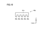
- FIG. 10 is a schematic plan view showing an enlarged part of a bus bar included in the semiconductor device according to the fourth embodiment.
- FIG. 11 is a schematic plan view showing an enlarged part of the semiconductor device according to the sixth embodiment.
- one of the purposes of the present disclosure is to provide a semiconductor device capable of improving the yield and reliability.
- the semiconductor device includes a drain terminal, a source terminal, and a gate terminal.
- the semiconductor device includes a first metal plate, a second metal plate arranged at intervals from the first metal plate, and a third metal arranged at intervals from each of the first metal plate and the second metal plate.
- the SiC transistor chip is provided with a second SiC transistor chip which is plate-shaped and is mounted on a first metal plate adjacent to the first SiC transistor chip.
- the first metal plate and the drain terminal are electrically connected.
- the second metal plate and the source terminal are electrically connected.
- the third metal plate and the gate terminal are electrically connected.
- the first SiC transistor chip includes a first source electrode pad and a first gate electrode pad arranged on one side in the thickness direction, and a first drain electrode pad arranged on the other side in the thickness direction.
- the second SiC transistor chip includes a second source electrode pad and a second gate electrode pad arranged on one side in the thickness direction, and a second drain electrode pad arranged on the other side in the thickness direction. , including.
- the first drain electrode pad is joined to the first metal plate.
- the second drain electrode pad is joined to the first metal plate.
- the semiconductor device includes a first conductor that electrically connects each of the first source electrode pad and the second source electrode pad and the second metal plate, and the first gate electrode pad and the second gate electrode pad.
- a second conductor that electrically connects each to the third metal plate, and one first wire that electrically connects the first source electrode pad, the second source electrode pad, and the fourth metal plate. To prepare for. At least one end of the first wire is joined to the fourth metal plate.
- the first SiC transistor chip and the second SiC transistor chip are mounted next to each other on the first metal plate.
- Such a first SiC transistor chip and a second SiC transistor chip are electrically connected in parallel.
- the SiC transistor chip refers to a transistor chip having a semiconductor layer made of SiC (silicon carbide) as an operating layer.
- the SiC transistor chip has low on-resistance and high withstand voltage. Therefore, the semiconductor device of the present disclosure adopting the above configuration in which a plurality of SiC transistor chips are connected in parallel can pass a large current.
- switching timing shifts may occur due to variations in the characteristics of each SiC transistor chip, and as a result, parasitic oscillation may occur. Since such parasitic oscillation may damage the transistor chip, it is required to suppress the parasitic oscillation.
- the first source electrode pad and the second source electrode pad are connected by the conductive first wire. Therefore, the potentials of the first source electrode pad and the second source electrode pad can be made the same. Therefore, parasitic oscillation can be suppressed.
- first source electrode pad and the second source electrode pad are electrically connected by the first wire, they may be connected by using wire bonding.
- wire connection using wire bonding each member and wire are connected one after another by ultrasonic bonding, and then the wire is finally cut.
- the blade of the cutter is pressed against the wire to cut the wire. If the SiC transistor chip comes into contact with the cutter blade when the wire is cut, the SiC transistor chip may be damaged. As a result, the yield at the time of manufacturing the semiconductor device is lowered.
- the semiconductor device of the present disclosure at least one end of the first wire is joined to the fourth metal plate. Therefore, the blade of the cutter can be pressed against the fourth metal plate to cut the wire. Therefore, it is possible to prevent the SiC transistor chip from coming into contact with the blade of the cutter when the wire is cut, and it is possible to reduce the risk of damage to the SiC transistor chip. Unlike the first metal plate connected to the drain terminal, a large current does not flow through the fourth metal plate. Therefore, even if the cutter blade is damaged, the reliability of the semiconductor device is not impaired. Therefore, it is possible to suppress a decrease in the yield of the semiconductor device at the time of manufacturing. From the above, according to the semiconductor device of the present disclosure, it is possible to improve the yield and the reliability.
- the above semiconductor device may further include a Kelvin terminal.
- the fourth metal plate and the Kelvin terminal may be electrically connected.
- a Kelvin terminal for controlling the gate voltage may be provided from the viewpoint of removing the influence of the parasitic inductance of the SiC transistor chips and reducing the switching loss.
- the Kelvin terminal forms a closed circuit with the gate terminal, and a large current does not flow. Therefore, in such a semiconductor device, the fourth metal plate can be effectively used as a configuration in which the fourth metal plate is connected to the Kelvin terminal, and the switching operation can be speeded up.
- the fourth metal plate may not be connected to each of the first metal plate, the second metal plate, and the third metal plate. By doing so, it is possible to obtain a fourth metal plate that is an electrically independent member, and even if the blade of the cutter comes into contact with the fourth metal plate and the fourth metal plate is damaged, the function as a semiconductor device is not impaired. Can be.
- the first wire may be arranged at a distance from each of the first conductor and the second conductor when viewed in the thickness direction of the first metal plate.
- the first conductor may be a bus bar (electrode plate).
- the parasitic inductance can be further reduced as compared with the case of connecting with a wire.
- soldering the bus bar it is possible to eliminate damage to the SiC transistor chip during wire bonding in connection using wires. Therefore, such a semiconductor device can further improve the yield and reliability.
- the first conductor may be a conductive second wire. By doing so, it is possible to electrically connect using the second wire in the same process as the first wire, and it is possible to improve the manufacturing efficiency.
- only one first wire may be used. By doing so, it is possible to improve the manufacturing efficiency.
- the semiconductor device of the present disclosure includes a drain terminal, a source terminal, a gate terminal, and a Kelvin terminal.
- the semiconductor device includes a first metal plate, a second metal plate arranged at intervals from the first metal plate, and a third metal arranged at intervals from each of the first metal plate and the second metal plate.
- the SiC transistor chip is provided with a second SiC transistor chip which is plate-shaped and is mounted on a first metal plate adjacent to the first SiC transistor chip. The first metal plate and the drain terminal are electrically connected.
- the second metal plate and the source terminal are electrically connected.
- the third metal plate and the gate terminal are electrically connected.
- the fourth metal plate and the Kelvin terminal are electrically connected.
- the fourth metal plate is not connected to each of the first metal plate, the second metal plate, and the third metal plate.
- the first SiC transistor chip includes a first source electrode pad and a first gate electrode pad arranged on one side in the thickness direction, and a first drain electrode pad arranged on the other side in the thickness direction. ,including.
- the second SiC transistor chip includes a second source electrode pad and a second gate electrode pad arranged on one side in the thickness direction, and a second drain electrode pad arranged on the other side in the thickness direction. ,including.
- the first drain electrode pad is joined to the first metal plate.
- the second drain electrode pad is joined to the first metal plate.
- the semiconductor device includes a first conductor that electrically connects each of the first source electrode pad and the second source electrode pad and the second metal plate, and the first gate electrode pad and the second gate electrode pad.
- a second conductor that electrically connects each to the third metal plate, and one first wire that electrically connects the first source electrode pad, the second source electrode pad, and the fourth metal plate.
- At least one end of the first wire is joined to the fourth metal plate.
- the first wire is arranged at a distance from each of the first conductor and the second conductor when viewed in the thickness direction of the first metal plate. There is only one first wire.
- FIG. 1 is a schematic plan view of the semiconductor device according to the first embodiment.
- FIG. 2 is a schematic plan view showing a part of the semiconductor device shown in FIG. 1 in an enlarged manner. In FIG. 2, the case described later shown in FIG. 1 is not shown.
- FIG. 3 is a schematic cross-sectional view showing a part of the semiconductor device shown in FIG. 1 in an enlarged manner.
- the semiconductor device 10a includes a drain terminal 31a, a source terminal 32a, a gate terminal 33a, and a Kelvin terminal 34a.
- the semiconductor device 10a includes a first metal plate 11a, a second metal plate 12a, a third metal plate 13a, a fourth metal plate 14a, and a first SiC transistor chip 21a arranged on the first metal plate 11a.
- a second SiC transistor chip 21b arranged on the first metal plate 11a, and a case 17a are included.
- the first metal plate 11a includes a substrate portion 15a having a rectangular shape when viewed in the thickness direction (Z direction) of the first metal plate 11a.
- the first metal plate 11a, the second metal plate 12a, the third metal plate 13a, and the fourth metal plate 14a constitute the lead frame 16a.
- the second metal plate 12a is arranged at a distance from the first metal plate 11a.
- the third metal plate 13a is arranged at a distance from each of the first metal plate 11a and the second metal plate 12a.
- the fourth metal plate 14a is arranged at intervals from each of the first metal plate 11a, the second metal plate 12a, and the third metal plate 13a.
- the semiconductor device 10a according to the first embodiment is a discrete device including a first SiC transistor chip 21a and a second SiC transistor chip 21b in a package.
- the first metal plate 11a, the second metal plate 12a, the third metal plate 13a, and the fourth metal plate 14a are each in the shape of a flat plate.
- a copper plate is adopted as the first metal plate 11a, the second metal plate 12a, the third metal plate 13a, and the fourth metal plate 14a.
- a thickness of this copper plate for example, one having a thickness of 1 mm is used.
- the first metal plate 11a and the drain terminal 31a are electrically connected to each other.
- the first metal plate 11a is integrally formed with the drain terminal 31a.
- the first metal plate 11a has a shape in which the drain terminal 31a is connected to the substrate portion 15a and is integrated.
- the second metal plate 12a and the source terminal 32a are electrically connected to each other.
- the second metal plate 12a is integrally formed with the source terminal 32a.
- the third metal plate 13a and the gate terminal 33a are electrically connected to each other.
- the third metal plate 13a is integrally formed with the gate terminal 33a.
- the fourth metal plate 14a and the Kelvin terminal 34a are electrically connected to each other.
- the fourth metal plate 14a is integrally formed with the Kelvin terminal 34a.
- the drain terminal 31a, the source terminal 32a, the gate terminal 33a, and the Kelvin terminal 34a each have a band-shaped shape.
- the drain terminal 31a, the source terminal 32a, the gate terminal 33a, and the Kelvin terminal 34a are arranged at intervals in the X direction, respectively.
- the drain terminal 31a, the source terminal 32a, the Kelvin terminal 34a, and the gate terminal 33a are arranged in this order in the direction of the arrow X.
- the semiconductor device 10a according to the first embodiment adopts a so-called four-terminal structure.
- An example of the boundary between the metal and the metal is shown by a broken line.
- the first SiC transistor chip 21a and the second SiC transistor chip 21b are so-called vertical semiconductor chips, for example, metal-oxide-semiconductor field effect transistors (MOSFETs).
- MOSFETs metal-oxide-semiconductor field effect transistors
- the first SiC transistor chip 21a and the second SiC transistor chip 21b are used as switching elements, respectively.
- the first SiC transistor chip 21a and the second SiC transistor chip 21b are connected in parallel.
- the first SiC transistor chip 21a and the second SiC transistor chip 21b each include a semiconductor layer made of silicon carbide (SiC) as an operating layer.
- SiC silicon carbide
- Such a first SiC transistor chip 21a and a second SiC transistor chip 21b have low on-resistance and high withstand voltage. Therefore, it is suitably used for semiconductor devices that carry a large current.
- the first SiC transistor chip 21a has a first drain electrode pad 22a located on one side in the thickness direction, a first source electrode pad 23a located on the other side in the thickness direction, and a first gate electrode pad. 24a and.
- the first drain electrode pad 22a of the first SiC transistor chip 21a is joined to the substrate portion 15a by, for example, solder (not shown). In this way, the first drain electrode pad 22a of the first SiC transistor chip 21a and the drain terminal 31a are electrically connected.
- the second SiC transistor chip 21b has a second drain electrode pad 22b located on one side in the thickness direction, a second source electrode pad 23b located on the other side in the thickness direction, and a second gate electrode pad. 24b and.
- the second drain electrode pad 22b of the second SiC transistor chip 21b is bonded to the substrate portion 15a by, for example, solder (not shown). In this way, the second drain electrode pad 22b of the second SiC transistor chip 21b and the drain terminal 31a are electrically connected.
- the first SiC transistor chip 21a and the second SiC transistor chip 21b are arranged on the substrate portion 15a at intervals in the Y direction, respectively. The positions of the first SiC transistor chip 21a and the second SiC transistor chip 21b in the X direction are the same.
- the case 17a is made of resin and is configured to cover the substrate portion 15a, the first SiC transistor chip 21a, the second SiC transistor chip 21b, and the wire described later.
- the case 17a has an insulating property. In this way, the substrate portion 15a, the first SiC transistor chip 21a, the second SiC transistor chip 21b, and the wire are sealed.
- the case 17a has a rectangular parallelepiped shape.
- the case 17a has a rectangular shape in which the length in the Y direction is longer than the length in the X direction when viewed in the thickness direction of the first metal plate 11a.
- the portions arranged in the case 17a constitute the first metal plate 11a, the second metal plate 12a, the third metal plate 13a, and the fourth metal plate 14, respectively.
- a portion exposed from one side of the rectangular case 17a constitutes a drain terminal 31a, a source terminal 32a, a gate terminal 33a, and a Kelvin terminal 34a, respectively. That is, in the present embodiment, the broken line indicates the boundary of the portion exposed from the case 17a.
- the case 17a is formed with a through hole 18a that penetrates in the thickness direction (Z direction).
- the first source electrode pad 23a of the first SiC transistor chip 21a is connected to the second metal plate 12a by two second wires 26a as the first conductor. Each of the two second wires 26a has conductivity. In this way, the first source electrode pad 23a of the first SiC transistor chip 21a is electrically connected to the source terminal 32a.
- the second source electrode pad 23b of the second SiC transistor chip 21b is connected to the second metal plate 12a by two second wires 26b as the first conductor. Each of the two second wires 26b has conductivity. In this way, the second source electrode pad 23b of the second SiC transistor chip 21b is electrically connected to the source terminal 32a.
- the first gate electrode pad 24a of the first SiC transistor chip 21a is connected to the third metal plate 13a by one third wire 27a as a second conductor.
- the third wire 27a has conductivity. In this way, the first gate electrode pad 24a of the first SiC transistor chip 21a is electrically connected to the gate terminal 33a.
- the second gate electrode pad 24b of the second SiC transistor chip 21b is connected to the third metal plate 13a by one third wire 27b as a second conductor.
- the third wire 27b has conductivity. In this way, the second gate electrode pad 24b of the second SiC transistor chip 21b is electrically connected to the gate terminal 33a.
- connection by the second wires 26a, 26b and the third wires 27a, 27b is carried out by using wire bonding, for example, using a wire bonder (not shown) equipped with a bond tool (not shown) from the viewpoint of manufacturing efficiency. be able to.
- the semiconductor device 10a includes one conductive first wire 28a.
- the first wire 28a electrically connects the first source electrode pad 23a, the second source electrode pad 23b, and the fourth metal plate 14a.
- One end 29a of the first wire 28a is joined to the first source electrode pad 23a.
- the other end 29c of the first wire 28a is joined to the fourth metal plate 14a.
- the first wire 28a is arranged at intervals from the second wires 26a and 26b, which are the first conductors, and the third wires 27a, 27b, which are the second conductors, when viewed in the thickness direction of the first metal plate 11a. Has been done. That is, the first wire 28a does not intersect the second wires 26a and 26b and the third wires 27a and 27b, respectively, when viewed in the thickness direction of the first metal plate 11a.
- the manufacturing method of the semiconductor device 10a will be briefly described.
- the first SiC transistor chip 21a and the second SiC transistor chip 21b are soldered to the substrate portion 15a. Join on top. Then, using wire bonding, each member is electrically connected by a wire.
- the joining of the first wire 28a is performed as follows. First, one end 29a of the wire, in this case, the tip of the wire is placed on the first source electrode pad 23a, and the tip of the wire bonder is pressed from above the wire. In such a state, one end 29a of the wire is ultrasonically bonded to the first source electrode pad 23a. Next, the wire bonder is moved onto the second source electrode pad 23b of the second SiC transistor chip 21b while supplying the wire. Then, at the bonding portion 29b, the wire and the first source electrode pad 23a are ultrasonically bonded by a wire bonder. Next, the wire supply unit is moved onto the fourth metal plate 14a while supplying the wire.
- the wire and the fourth metal plate 14a are ultrasonically bonded by a wire bonder.
- the cutter is pressed against the wire of the ultrasonically bonded portion to cut the wire.
- the other end 29c of the wire will be joined to the fourth metal plate 14a. In this way, the first wire 28a is joined.
- the other end 29c of the first wire 28a is joined to the fourth metal plate 14a. Therefore, the blade of the cutter can be pressed onto the fourth metal plate 14a to cut the wire. Therefore, when the wire is cut, the contact between the first SiC transistor chip 21a and the second SiC transistor chip 21b and the blade of the cutter can be prevented, and the first SiC transistor chip 21a and the second SiC transistor can be prevented. The risk of damage to the chip 21b can be reduced. Therefore, it is possible to suppress a decrease in the yield of the semiconductor device 10a at the time of manufacturing. As a result, such a semiconductor device 10a can improve the yield and the reliability.
- the fourth metal plate 14a and the Kelvin terminal 34a are electrically connected. Therefore, it is possible to reduce the switching loss by removing the influence of the parasitic inductance of the first SiC transistor chip 21a and the second SiC transistor chip 21b. Further, the Kelvin terminal 34a forms a closed circuit with the gate terminal 33a, and a large current does not flow. Therefore, such a semiconductor device 10a is a semiconductor device capable of effectively utilizing the fourth metal plate 14a as a configuration in which the fourth metal plate 14a is connected to the Kelvin terminal 34a and speeding up the switching operation. There is.
- the first wire 28a is a first conductor, the second wire 26a, 26b, and the second conductor, the third wire 27a, 27b, respectively, when viewed in the thickness direction of the first metal plate 11a. And are arranged at intervals. Therefore, it is possible to reduce the possibility that the first wire 28a and the second wires 26a and 26b and the third wires 27a and 27b each interfere with each other. Therefore, the semiconductor device 10a is a semiconductor device that facilitates wire bonding and can improve manufacturing efficiency.
- the first conductor is the conductive second wires 26a and 26b. Therefore, the second wires 26a and 26b can be used for electrical connection in the same process as the first wire 28a. Therefore, the semiconductor device 10a is a semiconductor device capable of improving manufacturing efficiency. In this embodiment, the third wires 27a and 27b can be used for connection in the same process as the first wire 28a.
- the semiconductor device 10a includes a drain terminal 31a, a source terminal 32a, a gate terminal 33a, and a Kelvin terminal 34a.
- the semiconductor device 10a is spaced from the first metal plate 11a, the second metal plate 12a arranged at intervals from the first metal plate 11a, and the first metal plate 11a and the second metal plate 12a, respectively.
- a transistor chip 21b is provided.
- the first metal plate 11a and the drain terminal 31a are electrically connected to each other.
- the second metal plate 12a and the source terminal 32a are electrically connected to each other.
- the third metal plate 13a and the gate terminal 33a are electrically connected to each other.
- the fourth metal plate 14a and the Kelvin terminal 34a are electrically connected to each other.
- the fourth metal plate 14a is not connected to each of the first metal plate 11a, the second metal plate 12a, and the third metal plate 13a.
- the first SiC transistor chip 21a has a first source electrode pad 23a and a first gate electrode pad 24a arranged on one side in the thickness direction, and a first drain arranged on the other side in the thickness direction.
- the electrode pad 22a and the like are included.
- the second SiC transistor chip 21b has a second source electrode pad 23b and a second gate electrode pad 24b arranged on one side in the thickness direction, and a second drain arranged on the other side in the thickness direction. Includes electrode pads 22b and.
- the first drain electrode pad 22a is joined to the first metal plate 11a.
- the second drain electrode pad 22b is joined to the first metal plate 11a.
- the second wires 26a and 26b as the first conductor for electrically connecting each of the first source electrode pad 23a and the second source electrode pad 23b and the second metal plate 12a, and the first one.
- the third wires 27a and 27b as the second conductor for electrically connecting each of the gate electrode pads 24a and the second gate electrode pads 24b and the third metal plate 13a, and the first source electrode pads 23a and the first.
- a first wire 28a for electrically connecting the source electrode pad 23b of 2 and the fourth metal plate 14a is provided.
- the other end 29c of the first wire 28a is joined to the fourth metal plate 14a.
- the first wire 28a is arranged at intervals from the second wires 26a and 26b, which are the first conductors, and the third wires 27a, 27b, which are the second conductors, when viewed in the thickness direction of the first metal plate 11a. Has been done. There is only one first wire 28a.
- FIG. 4 is a schematic plan view showing an enlarged part of the semiconductor device according to the second embodiment.
- the semiconductor device of the second embodiment is different from the case of the first embodiment in that the second wires, which are the first conductors, intersect with each other when viewed in the thickness direction of the first metal plate 11a.
- the positions of the first SiC transistor chip 21a and the second SiC transistor chip 21b included in the semiconductor device 10b of the second embodiment are different in the X direction.
- the second SiC transistor chip 21b is arranged so as to be closer to the drain terminal 31a than the first SiC transistor chip 21a.
- the second wire 26a as the first conductor intersects the second wire 26b when viewed in the thickness direction of the first metal plate 11a.
- the semiconductor device 10b is a semiconductor device capable of improving reliability. In the present embodiment, it is possible to increase the degree of freedom in the arrangement and orientation of the first SiC transistor chip 21a and the second SiC transistor chip 21b on the substrate portion 15a.
- FIG. 5 is a schematic plan view showing an enlarged part of the semiconductor device according to the third embodiment.
- the semiconductor device of the third embodiment is different from the case of the first embodiment and the second embodiment in that the Kelvin terminal is not included and the first wire intersects the second conductor.
- the positions of the first SiC transistor chip 21a and the second SiC transistor chip 21b included in the semiconductor device 10c of the third embodiment are different in the X direction.
- the first SiC transistor chip 21a is arranged so as to be closer to the drain terminal 31a than the second SiC transistor chip 21b.
- the first wire 28a intersects with the third wire 27a as the second conductor when viewed in the thickness direction of the first metal plate 11a.
- the fourth metal plate 14a included in the semiconductor device 10c of the third embodiment is not exposed from the case 17a.
- the semiconductor device 10c of the third embodiment does not include the Kelvin terminal 34a included in the semiconductor devices 10a and 10b of the first embodiment and the second embodiment.
- the semiconductor device 10c according to the third embodiment adopts a three-terminal structure.
- the fourth metal plate 14a is not connected to any of the first metal plate 11a, the second metal plate 12a, and the third metal plate 13a.
- the fourth metal plate 14a is used for cutting the first wire 28a during manufacturing.
- the semiconductor device 10c of the present embodiment is a semiconductor device capable of improving reliability.
- the semiconductor device 10c of the present embodiment is preferably used when adopting a three-terminal structure without a Kelvin terminal.
- the semiconductor device may be configured to incorporate a diode chip that suppresses the flow of current in the reverse direction in the electric circuit. By doing so, the risk of damage to the first SiC transistor chip 21a and the second SiC transistor chip 21b can be reduced, and the reliability of the semiconductor device can be further improved.
- FIG. 6 is a schematic plan view showing an enlarged part of the semiconductor device according to the fourth embodiment.
- FIG. 7 is a schematic side view when a part of the semiconductor device shown in FIG. 6 is viewed in the direction indicated by the arrow X.
- FIG. 8 is a schematic side view of a part of the semiconductor device shown in FIG. 6 when viewed in the Y direction.
- FIG. 9 is a schematic side view when a part of the semiconductor device shown in FIG. 6 is viewed in the direction opposite to the direction indicated by the arrow X.
- the semiconductor device of the fourth embodiment is different from the case of the first embodiment in that a bus bar (electrode plate) is used instead of the wire as the first conductor and that the semiconductor device has a diode chip.
- a bus bar electrode plate
- the semiconductor device 10d of the fourth embodiment includes a first metal plate 11a, a second metal plate 12a, a third metal plate 13a, and a fourth metal.
- the case 17d is formed so as to surround the substrate portion 15a.
- the diode chip 36a is a so-called vertical semiconductor chip, for example, a Schottky barrier diode (SBD).
- SBD Schottky barrier diode
- a SiC diode chip including a semiconductor layer made of silicon carbide (SiC) as an operating layer is adopted from the viewpoint of low on-resistance and high withstand voltage.
- the diode chip 36a is arranged on the first metal plate 11a. In the present embodiment, the diode chip 36a is arranged on the substrate portion 15a of the first metal plate 11a.
- the diode chip 36a has a plate shape.
- the diode chip 36a includes a cathode electrode pad 37a located on one side in the thickness direction and an anode electrode pad 38a located on the other side in the thickness direction.
- the diode chip 36a is arranged on the substrate portion 15a by joining the cathode electrode pad 37a to the substrate portion 15a, for example, by soldering (not shown). By adopting a configuration including such a diode chip 36a, it is possible to suppress the flow of current in the reverse direction.
- the bus bar 40a has, for example, a bent steel strip.
- the bus bar 40a is connected to a band-shaped first portion 41a extending in the Y direction and a first portion 41a, and is connected to a second portion 42a bent in a semicircular shape in the thickness direction and a second portion 42a, and is in a flat plate shape. It includes a third portion 43a, a fourth portion 44a extending in an inclined manner connected to the third portion 43a, and a flat plate-shaped fifth portion 45a connected to the fourth portion 44a and parallel to the third portion 43a.
- the first portion 41a is arranged so as to straddle the first SiC transistor chip 21a and the second SiC transistor chip 21b.
- the third portion 43a is arranged on the diode chip 36a.
- the fifth portion 45a is arranged on the second metal plate 12a constituting the lead frame 16a.
- the first portion 41a, the first SiC transistor chip 21a, and the second SiC transistor chip 21b are each joined by solder (not shown).
- the third portion 43a and the diode chip 36a are joined by solder (not shown).
- the fifth portion 45a and the second metal plate 12a are joined by solder (not shown).
- the first conductor connecting each of the first source electrode pad 23a and the second source electrode pad 23b to the second metal plate 12a is a bus bar 40a.
- the parasitic inductance can be further reduced as compared with the case of connecting with a wire.
- soldering the bus bar 40a it is possible to eliminate damage to the first SiC transistor chip 21a and the second SiC transistor chip 21b during wire bonding in the connection using wires. Therefore, such a semiconductor device 10d is a semiconductor device capable of further improving the yield and reliability.
- FIG. 10 is a schematic plan view showing an enlarged part of a bus bar included in the semiconductor device according to the fourth embodiment.
- the semiconductor device of the fifth embodiment is different from the case of the fourth embodiment in the shape of the first portion of the bus bar.
- the first portion 41b of the bus bar 40b included in the semiconductor device of the fifth embodiment includes a plurality of protrusions 46b.
- the protrusions 46b are formed so as to extend in the Z direction with a gap in the Y direction.
- the tip of the protrusion 46b in the Z direction is formed of a flat surface.
- it is joined to each of the first SiC transistor chip 21a and the second SiC transistor chip 21b.
- FIG. 11 is a schematic plan view showing an enlarged part of the semiconductor device according to the sixth embodiment.
- the semiconductor device 10e of the sixth embodiment includes a first metal plate 11a, a second metal plate 12a, a third metal plate 13a, a fourth metal plate 14a, and a first metal plate 11a.
- the first conductor connecting each of the first source electrode pad 23a and the second source electrode pad 23b to the second metal plate 12a is a bus bar 40a.
- the parasitic inductance can be further reduced. Therefore, such a semiconductor device 10e is a semiconductor device capable of further improving the yield and reliability.
- the SiC transistor chip is included, but the present invention is not limited to this, and the operating layer may include another semiconductor layer, for example, a semiconductor layer composed of gallium nitride or gallium oxide. good.
- SiC transistor chips connected in parallel are included, but the present invention is not limited to this, and three or more SiC transistor chips connected in parallel may be included.
- the number of the first wire is only one, but the present invention is not limited to this, and two or more first wires, that is, a plurality of the first wires may be included.
- the present invention is not limited to this, and one end of the first wire is the fourth metal plate. It may be joined to. Further, both ends of the first wire may be joined to the fourth metal plate. In this case, a plurality of fourth metal plates may be provided.
- the first metal plate 11a and the drain terminal 31a are integrally configured, but the present invention is not limited to this, and the first metal plate 11a and the drain terminal 31a are each configured. It is composed of a separate member, and the first metal plate 11a and the drain terminal 31a may be electrically connected by a member having conductivity.
- the second metal plate 12a and the source terminal 32a may be electrically connected by a conductive member.
- the third metal plate 13a and the gate terminal 33a are integrally configured, but the present invention is not limited to this, and the third metal plate 13a and the gate terminal 33a are each composed of separate members, and the third metal plate 13a and the gate terminal 33a are configured as separate members.
- the metal plate 13a and the gate terminal 33a may be electrically connected by a conductive member.
- the fourth metal plate 14a and the Kelvin terminal 34a are integrally configured, but the present invention is not limited to this, and the fourth metal plate 14a and the Kelvin terminal 34a are each composed of separate members, and the fourth metal plate 14a and the Kelvin terminal 34a are configured as separate members.
- the metal plate 14a and the Kelvin terminal 34a may be electrically connected by a conductive member.
- 10a, 10b, 10c, 10d, 10e Semiconductor device, 11a 1st metal plate, 12a 2nd metal plate, 13a 3rd metal plate, 14a 4th metal plate, 15a substrate part, 16a lead frame, 17a, 17d case, 18a Through hole, 21a first SiC transistor chip, 21b second SiC transistor chip, 22a first drain electrode pad, 22b second drain electrode pad, 23a first source electrode pad, 23b second source electrode pad , 24a 1st gate electrode pad, 24b 2nd gate electrode pad, 26a, 26b 2nd wire, 27a, 27b 3rd wire, 28a 1st wire, 29a, 29c end, 29b joint, 31a drain terminal, 32a source terminal, 33a gate terminal, 34a Kelvin terminal, 36a diode chip, 37a cathode electrode pad, 38a anode electrode pad, 40a, 40b bus bar, 41a, 41b 1st part, 42a 2nd part, 43a 3rd part, 44a 1st 4 parts
Landscapes
- Junction Field-Effect Transistors (AREA)
- Electrodes Of Semiconductors (AREA)
Abstract
ドレイン端子と、ソース端子と、ゲート端子と、を含む半導体装置は、第1金属板と、第2金属板と、第3金属板と、第4金属板と、第1のSiCトランジスタチップと、第2のSiCトランジスタチップと、を備える。半導体装置は、第1導体と、第2導体と、第1のソース電極パッド、第2のソース電極パッドおよび第4金属板を電気的に接続する1本の第1ワイヤと、を備える。第1ワイヤの少なくともいずれか一方の端部は、第4金属板に接合されている。
Description
本開示は、半導体装置に関するものである。
本出願は、2020年9月1日出願の日本出願第2020-146874号に基づく優先権を主張し、前記日本出願に記載された全ての記載内容を援用するものである。
パッケージ化された半導体デバイスが知られている(たとえば、特許文献1参照)。特許文献1に開示の半導体デバイスは、対向する2つのパワーデバイスダイを有する。
本開示に従った半導体装置は、ドレイン端子と、ソース端子と、ゲート端子と、を含む。半導体装置は、第1金属板と、第1金属板と間隔をあけて配置される第2金属板と、第1金属板および第2金属板のそれぞれと間隔をあけて配置される第3金属板と、第1金属板、第2金属板および第3金属板のそれぞれと間隔をあけて配置される第4金属板と、板状であって、第1金属板上に搭載される第1のSiCトランジスタチップと、板状であって、第1のSiCトランジスタチップと隣り合って第1金属板上に搭載される第2のSiCトランジスタチップと、を備える。第1金属板とドレイン端子とは、電気的に接続されている。第2金属板とソース端子とは、電気的に接続されている。第3金属板とゲート端子とは、電気的に接続されている。第1のSiCトランジスタチップは、厚さ方向の一方側に配置される第1のソース電極パッドおよび第1のゲート電極パッドと、厚さ方向の他方側に配置される第1のドレイン電極パッドと、を含む。第2のSiCトランジスタチップは、厚さ方向の一方側に配置される第2のソース電極パッドおよび第2のゲート電極パッドと、厚さ方向の他方側に配置される第2のドレイン電極パッドと、を含む。第1のドレイン電極パッドは、第1金属板に接合されている。第2のドレイン電極パッドは、第1金属板に接合されている。半導体装置は、第1のソース電極パッドおよび第2のソース電極パッドのそれぞれと第2金属板とを電気的に接続する第1導体と、第1のゲート電極パッドおよび第2のゲート電極パッドのそれぞれと第3金属板とを電気的に接続する第2導体と、第1のソース電極パッド、第2のソース電極パッドおよび第4金属板を電気的に接続する1本の第1ワイヤと、を備える。第1ワイヤの少なくともいずれか一方の端部は、第4金属板に接合されている。
[本開示が解決しようとする課題]
特許文献1に開示の半導体デバイスによると、部品点数が多く、複雑な製造であるため、高コストとなってしまう。また昨今、半導体装置において大電流を流すことができる観点から、トランジスタチップにおいてSiトランジスタチップに替え、SiCトランジスタチップを用いる場合がある。SiCトランジスタチップは、Siトランジスタチップと異なり、チップの製造時における歩留まりが劣る。よって、比較的面積の小さいSiCトランジスタチップを複数並列に接続した構成が採用される場合がある。複数のSiCトランジスタチップを用いた半導体装置において、半導体装置の製造時にSiCトランジスタチップが損傷すると、歩留まりおよび信頼性が低下してしまうこととなる。歩留まりの向上および信頼性の向上を図ることができる半導体装置が求められる。
特許文献1に開示の半導体デバイスによると、部品点数が多く、複雑な製造であるため、高コストとなってしまう。また昨今、半導体装置において大電流を流すことができる観点から、トランジスタチップにおいてSiトランジスタチップに替え、SiCトランジスタチップを用いる場合がある。SiCトランジスタチップは、Siトランジスタチップと異なり、チップの製造時における歩留まりが劣る。よって、比較的面積の小さいSiCトランジスタチップを複数並列に接続した構成が採用される場合がある。複数のSiCトランジスタチップを用いた半導体装置において、半導体装置の製造時にSiCトランジスタチップが損傷すると、歩留まりおよび信頼性が低下してしまうこととなる。歩留まりの向上および信頼性の向上を図ることができる半導体装置が求められる。
そこで、歩留まりの向上および信頼性の向上を図ることができる半導体装置を提供することを本開示の目的の1つとする。
[本開示の効果]
上記半導体装置によれば、歩留まりの向上および信頼性の向上を図ることができる。
上記半導体装置によれば、歩留まりの向上および信頼性の向上を図ることができる。
[本開示の実施形態の説明]
最初に本開示の実施態様を列記して説明する。本開示に係る半導体装置は、ドレイン端子と、ソース端子と、ゲート端子と、を含む。半導体装置は、第1金属板と、第1金属板と間隔をあけて配置される第2金属板と、第1金属板および第2金属板のそれぞれと間隔をあけて配置される第3金属板と、第1金属板、第2金属板および第3金属板のそれぞれと間隔をあけて配置される第4金属板と、板状であって、第1金属板上に搭載される第1のSiCトランジスタチップと、板状であって、第1のSiCトランジスタチップと隣り合って第1金属板上に搭載される第2のSiCトランジスタチップと、を備える。第1金属板とドレイン端子とは、電気的に接続されている。第2金属板とソース端子とは、電気的に接続されている。第3金属板とゲート端子とは、電気的に接続されている。第1のSiCトランジスタチップは、厚さ方向の一方側に配置される第1のソース電極パッドおよび第1のゲート電極パッドと、厚さ方向の他方側に配置される第1のドレイン電極パッドと、を含む。第2のSiCトランジスタチップは、厚さ方向の一方側に配置される第2のソース電極パッドおよび第2のゲート電極パッドと、厚さ方向の他方側に配置される第2のドレイン電極パッドと、を含む。第1のドレイン電極パッドは、第1金属板に接合されている。第2のドレイン電極パッドは、第1金属板に接合されている。半導体装置は、第1のソース電極パッドおよび第2のソース電極パッドのそれぞれと第2金属板とを電気的に接続する第1導体と、第1のゲート電極パッドおよび第2のゲート電極パッドのそれぞれと第3金属板とを電気的に接続する第2導体と、第1のソース電極パッド、第2のソース電極パッドおよび第4金属板を電気的に接続する1本の第1ワイヤと、を備える。第1ワイヤの少なくともいずれか一方の端部は、第4金属板に接合されている。
最初に本開示の実施態様を列記して説明する。本開示に係る半導体装置は、ドレイン端子と、ソース端子と、ゲート端子と、を含む。半導体装置は、第1金属板と、第1金属板と間隔をあけて配置される第2金属板と、第1金属板および第2金属板のそれぞれと間隔をあけて配置される第3金属板と、第1金属板、第2金属板および第3金属板のそれぞれと間隔をあけて配置される第4金属板と、板状であって、第1金属板上に搭載される第1のSiCトランジスタチップと、板状であって、第1のSiCトランジスタチップと隣り合って第1金属板上に搭載される第2のSiCトランジスタチップと、を備える。第1金属板とドレイン端子とは、電気的に接続されている。第2金属板とソース端子とは、電気的に接続されている。第3金属板とゲート端子とは、電気的に接続されている。第1のSiCトランジスタチップは、厚さ方向の一方側に配置される第1のソース電極パッドおよび第1のゲート電極パッドと、厚さ方向の他方側に配置される第1のドレイン電極パッドと、を含む。第2のSiCトランジスタチップは、厚さ方向の一方側に配置される第2のソース電極パッドおよび第2のゲート電極パッドと、厚さ方向の他方側に配置される第2のドレイン電極パッドと、を含む。第1のドレイン電極パッドは、第1金属板に接合されている。第2のドレイン電極パッドは、第1金属板に接合されている。半導体装置は、第1のソース電極パッドおよび第2のソース電極パッドのそれぞれと第2金属板とを電気的に接続する第1導体と、第1のゲート電極パッドおよび第2のゲート電極パッドのそれぞれと第3金属板とを電気的に接続する第2導体と、第1のソース電極パッド、第2のソース電極パッドおよび第4金属板を電気的に接続する1本の第1ワイヤと、を備える。第1ワイヤの少なくともいずれか一方の端部は、第4金属板に接合されている。
本開示の半導体装置によると、第1のSiCトランジスタチップと第2のSiCトランジスタチップとが隣り合って、それぞれ第1金属板上に搭載されている。このような第1のSiCトランジスタチップと第2のSiCトランジスタチップは、電気的に並列に接続された構成となる。SiCトランジスタチップとは、SiC(炭化珪素)から構成される半導体層を動作層として有するトランジスタチップをいう。SiCトランジスタチップは、低オン抵抗かつ高耐圧である。よって、複数のSiCトランジスタチップが並列に接続された上記構成を採用する本開示の半導体装置は、大電流を流すことができる。
並列に接続されたSiCトランジスタチップを採用する半導体装置においては、各SiCトランジスタチップの特性のばらつきに起因して、スイッチングのタイミングのずれが生じ、その結果、寄生発振が生ずるおそれがある。このような寄生発振は、トランジスタチップにダメージを与えるおそれがあるため、寄生発振を抑制することが求められる。
本開示の半導体装置によると、導電性の第1ワイヤにより第1のソース電極パッドと第2のソース電極パッドとが接続されている。よって、第1のソース電極パッドと第2のソース電極パッドとの電位を同じにすることができる。したがって、寄生発振を抑制することができる。
製造効率の観点から、第1のソース電極パッドと第2のソース電極パッドとを第1ワイヤにより電気的に接続する際に、ワイヤボンディングを利用して接続する場合がある。ワイヤボンディングを利用したワイヤの接続においては、超音波接合により各部材とワイヤとを次々に接続した後、最終的にワイヤを切断する。この場合、第1のソース電極パッドと第2のソース電極パッドとをワイヤにより接続した後、カッターの刃をワイヤに押し当てて、ワイヤを切断する。ワイヤの切断時にSiCトランジスタチップとカッターの刃が接触すると、SiCトランジスタチップが損傷してしまうおそれがある。その結果、半導体装置の製造時における歩留まりが低下してしまうこととなる。
本開示の半導体装置によると、第1ワイヤの少なくともいずれか一方の端部は、第4金属板に接合されている。よって、第4金属板の上でカッターの刃を押し当て、ワイヤを切断することができる。したがって、ワイヤの切断時において、SiCトランジスタチップとカッターの刃との接触を防止することができ、SiCトランジスタチップが損傷するおそれを低減することができる。第4金属板には、ドレイン端子と接続される第1金属板のように大電流が流れない。よって、カッターの刃による損傷を受けても、半導体装置の信頼性を損ねることはない。したがって、製造時において半導体装置の歩留まりの低下を抑制することができる。以上より、本開示の半導体装置によると、歩留まりの向上および信頼性の向上を図ることができる。
上記半導体装置は、ケルビン端子をさらに含んでもよい。第4金属板とケルビン端子とは、電気的に接続されていてもよい。並列に接続されたSiCトランジスタチップを採用する半導体装置において、SiCトランジスタチップの寄生インダクタンスの影響を取り除き、スイッチング損失の低減を図る観点から、ゲート電圧の制御用のケルビン端子を設ける場合がある。ケルビン端子は、ゲート端子と閉回路を形成し、大電流が流れることはない。よって、このような半導体装置は、第4金属板がケルビン端子と接続される構成として第4金属板を有効利用し、スイッチング動作の高速化を図ることができる。
上記半導体装置において、第4金属板は、第1金属板、第2金属板および第3金属板のそれぞれと接続されていなくてもよい。このようにすることにより、電気的に独立した部材とした第4金属板とすることができ、カッターの刃が接触して第4金属板が損傷しても、半導体装置としての機能を損ねないものとすることができる。
上記半導体装置において、第1ワイヤは、第1金属板の厚さ方向に見て、第1導体および第2導体のそれぞれと間隔をあけて配置されてもよい。このようにすることにより、第1ワイヤと、第1導体および第2導体のそれぞれとが干渉するおそれを低減することができる。したがって、ワイヤボンディングの実施が容易となり、製造効率の向上を図ることができる。
上記半導体装置において、第1導体は、バスバー(電極板)であってもよい。このようにすることにより、ワイヤで接続する場合に比べて寄生インダクタンスをさらに低減することができる。また、バスバーをはんだ付けすることで、ワイヤを用いた接続におけるワイヤボンディング時のSiCトランジスタチップの損傷を除外することができる。したがって、このような半導体装置は、より歩留まりの向上および信頼性の向上を図ることができる。
上記半導体装置において、第1導体は、導電性の第2ワイヤであってもよい。このようにすることにより、第1ワイヤと同様の工程で第2ワイヤを用いて電気的に接続することができ、製造効率の向上を図ることができる。
上記半導体装置において、第1ワイヤは、1本のみであってもよい。このようにすることにより、製造効率の向上を図ることができる。
また、本開示の半導体装置は、ドレイン端子と、ソース端子と、ゲート端子と、ケルビン端子と、を含む。半導体装置は、第1金属板と、第1金属板と間隔をあけて配置される第2金属板と、第1金属板および第2金属板のそれぞれと間隔をあけて配置される第3金属板と、第1金属板、第2金属板および第3金属板のそれぞれと間隔をあけて配置される第4金属板と、板状であって、第1金属板上に搭載される第1のSiCトランジスタチップと、板状であって、第1のSiCトランジスタチップと隣り合って第1金属板上に搭載される第2のSiCトランジスタチップと、を備える。第1金属板とドレイン端子とは、電気的に接続されている。第2金属板とソース端子とは、電気的に接続されている。第3金属板とゲート端子とは、電気的に接続されている。第4金属板とケルビン端子とは、電気的に接続されている。第4金属板は、第1金属板、第2金属板および第3金属板のそれぞれと接続されていない。第1のSiCトランジスタチップは、厚さ方向の一方側に配置される第1のソース電極パッドおよび第1のゲート電極パッドと、厚さ方向の他方側に配置される第1のドレイン電極パッドと、を含む。第2のSiCトランジスタチップは、厚さ方向の一方側に配置される第2のソース電極パッドおよび第2のゲート電極パッドと、厚さ方向の他方側に配置される第2のドレイン電極パッドと、を含む。第1のドレイン電極パッドは、第1金属板に接合されている。第2のドレイン電極パッドは、第1金属板に接合されている。半導体装置は、第1のソース電極パッドおよび第2のソース電極パッドのそれぞれと第2金属板とを電気的に接続する第1導体と、第1のゲート電極パッドおよび第2のゲート電極パッドのそれぞれと第3金属板とを電気的に接続する第2導体と、第1のソース電極パッド、第2のソース電極パッドおよび第4金属板を電気的に接続する1本の第1ワイヤと、を備える。第1ワイヤの少なくともいずれか一方の端部は、第4金属板に接合されている。第1ワイヤは、第1金属板の厚さ方向に見て、第1導体および第2導体のそれぞれと間隔をあけて配置されている。第1ワイヤは、1本のみである。
このような半導体装置によると、歩留まりの向上および信頼性の向上を図ることができる。また、半導体装置としての機能を損ねず、スイッチング動作の高速化を図りながら、製造効率の向上を図ることができる。
[本開示の実施形態の詳細]
次に、本開示の半導体装置の実施形態を、図面を参照しつつ説明する。以下の図面において同一または相当する部分には同一の参照符号を付しその説明は繰り返さない。
次に、本開示の半導体装置の実施形態を、図面を参照しつつ説明する。以下の図面において同一または相当する部分には同一の参照符号を付しその説明は繰り返さない。
(実施の形態1)
本開示の実施の形態1における半導体装置の構成について説明する。図1は、実施の形態1における半導体装置の概略平面図である。図2は、図1に示す半導体装置の一部を拡大して示す概略平面図である。図2においては、図1中に示す後述するケースの図示を省略している。図3は、図1に示す半導体装置の一部を拡大して示す概略断面図である。
本開示の実施の形態1における半導体装置の構成について説明する。図1は、実施の形態1における半導体装置の概略平面図である。図2は、図1に示す半導体装置の一部を拡大して示す概略平面図である。図2においては、図1中に示す後述するケースの図示を省略している。図3は、図1に示す半導体装置の一部を拡大して示す概略断面図である。
図1、図2および図3を参照して、実施の形態1における半導体装置10aは、ドレイン端子31aと、ソース端子32aと、ゲート端子33aと、ケルビン端子34aと、を含む。半導体装置10aは、第1金属板11aと、第2金属板12aと、第3金属板13aと、第4金属板14aと、第1金属板11a上に配置される第1のSiCトランジスタチップ21aと、第1金属板11a上に配置される第2のSiCトランジスタチップ21bと、ケース17aと、を含む。第1金属板11aは、第1金属板11aの厚さ方向(Z方向)に見て矩形状の基板部15aを含む。第1金属板11a、第2金属板12a、第3金属板13aおよび第4金属板14aは、リードフレーム16aを構成する。第2金属板12aは、第1金属板11aと間隔をあけて配置される。第3金属板13aは、第1金属板11aおよび第2金属板12aのそれぞれと間隔をあけて配置される。第4金属板14aは、第1金属板11a、第2金属板12aおよび第3金属板13aのそれぞれと間隔をあけて配置される。実施の形態1における半導体装置10aは、第1のSiCトランジスタチップ21aおよび第2のSiCトランジスタチップ21bをパッケージ内に含むディスクリートデバイスである。
第1金属板11a、第2金属板12a、第3金属板13aおよび第4金属板14aはそれぞれ、平板状である。第1金属板11a、第2金属板12a、第3金属板13aおよび第4金属板14aとして、たとえば銅板が採用される。この銅板の厚さとしては、たとえば1mmのものが用いられる。第1金属板11aとドレイン端子31aとは、電気的に接続されている。本実施形態においては、第1金属板11aは、ドレイン端子31aと一体で構成されている。具体的には、第1金属板11aは、基板部15aにドレイン端子31aが接続され、一体とされた形状を有する。第2金属板12aとソース端子32aとは、電気的に接続されている。本実施形態においては、第2金属板12aは、ソース端子32aと一体で構成されている。第3金属板13aとゲート端子33aとは、電気的に接続されている。本実施形態においては、第3金属板13aは、ゲート端子33aと一体で構成されている。第4金属板14aとケルビン端子34aとは、電気的に接続されている。本実施形態においては、第4金属板14aは、ケルビン端子34aと一体で構成されている。ドレイン端子31a、ソース端子32a、ゲート端子33aおよびケルビン端子34aはそれぞれ、帯状の形状を有する。ドレイン端子31a、ソース端子32a、ゲート端子33aおよびケルビン端子34aはそれぞれ、X方向に間隔をあけて配置されている。本実施形態においては、矢印Xの向きにドレイン端子31a、ソース端子32a、ケルビン端子34a、ゲート端子33aの順で配置される。実施の形態1における半導体装置10aは、いわゆる4端子構造を採用している。なお、第1金属板11aとドレイン端子31aとの境界、第2金属板12aとソース端子32aとの境界、第3金属板13aとゲート端子33aとの境界および第4金属板14aとケルビン端子34aとの境界の一例をそれぞれ破線で示している。
第1のSiCトランジスタチップ21aおよび第2のSiCトランジスタチップ21bはそれぞれ、いわゆる縦型の半導体チップであり、たとえば金属-酸化物-半導体電界効果型トランジスタ(MOSFET)である。本実施形態においては、第1のSiCトランジスタチップ21aおよび第2のSiCトランジスタチップ21bはそれぞれ、スイッチング素子として用いられる。第1のSiCトランジスタチップ21aおよび第2のSiCトランジスタチップ21bは並列に接続される。第1のSiCトランジスタチップ21aおよび第2のSiCトランジスタチップ21bはそれぞれ、炭化珪素(SiC)から構成される半導体層を動作層として含む。このような第1のSiCトランジスタチップ21aおよび第2のSiCトランジスタチップ21bは、低オン抵抗かつ高耐圧である。よって、大電流を流す半導体装置に好適に用いられる。
第1のSiCトランジスタチップ21aは、厚さ方向の一方側に位置する第1のドレイン電極パッド22aと、厚さ方向の他方側に位置する第1のソース電極パッド23aおよび第1のゲート電極パッド24aと、を含む。第1のSiCトランジスタチップ21aの第1のドレイン電極パッド22aは、たとえばはんだ(図示せず)により基板部15aに接合される。このようにして、第1のSiCトランジスタチップ21aの第1のドレイン電極パッド22aとドレイン端子31aとが電気的に接続される。第2のSiCトランジスタチップ21bは、厚さ方向の一方側に位置する第2のドレイン電極パッド22bと、厚さ方向の他方側に位置する第2のソース電極パッド23bおよび第2のゲート電極パッド24bと、を含む。第1のSiCトランジスタチップ21aの場合と同様に、第2のSiCトランジスタチップ21bの第2のドレイン電極パッド22bは、たとえばはんだ(図示せず)により基板部15aに接合される。このようにして、第2のSiCトランジスタチップ21bの第2のドレイン電極パッド22bとドレイン端子31aとが電気的に接続される。本実施形態においては、基板部15a上において、第1のSiCトランジスタチップ21aおよび第2のSiCトランジスタチップ21bはそれぞれ、Y方向に間隔をあけて配置される。なお、第1のSiCトランジスタチップ21aおよび第2のSiCトランジスタチップ21bのX方向の位置は、同じである。
ケース17aは、樹脂製であって、基板部15a、第1のSiCトランジスタチップ21a、第2のSiCトランジスタチップ21bおよび後述するワイヤを覆うように構成される。ケース17aは、絶縁性を有する。このようにして、基板部15a、第1のSiCトランジスタチップ21a、第2のSiCトランジスタチップ21bおよびワイヤが封止される。ケース17aは、直方体の形状を有する。ケース17aは、第1金属板11aの厚さ方向に見て、Y方向の長さがX方向の長さよりも長い矩形状を有する。ケース17a内に配置される部分がそれぞれ、第1金属板11a、第2金属板12a、第3金属板13aおよび第4金属板14を構成する。また、矩形状のケース17aの一辺から露出した部分がそれぞれ、ドレイン端子31a、ソース端子32a、ゲート端子33a、ケルビン端子34aを構成する。すなわち、本実施形態においては、破線は、ケース17aから露出する部分の境界を示している。半導体装置10aにおいては、ケルビン端子34aとの間で閉回路を形成するゲート端子33aの電圧を制御することにより、スイッチング動作の高速化を図りながら、ドレイン端子31aに大電流を流すことができる。なお、ケース17aには、厚さ方向(Z方向)に貫通する貫通孔18aが形成されている。
第1のSiCトランジスタチップ21aの第1のソース電極パッド23aは、第1導体としての2本の第2ワイヤ26aにより第2金属板12aに接続される。2本の第2ワイヤ26aはそれぞれ、導電性を有する。このようにして、第1のSiCトランジスタチップ21aの第1のソース電極パッド23aは、ソース端子32aと電気的に接続される。第2のSiCトランジスタチップ21bの第2のソース電極パッド23bは、第1導体としての2本の第2ワイヤ26bにより第2金属板12aに接続される。2本の第2ワイヤ26bはそれぞれ、導電性を有する。このようにして、第2のSiCトランジスタチップ21bの第2のソース電極パッド23bは、ソース端子32aと電気的に接続される。第1のSiCトランジスタチップ21aの第1のゲート電極パッド24aは、第2導体としての1本の第3ワイヤ27aにより第3金属板13aに接続される。第3ワイヤ27aは、導電性を有する。このようにして、第1のSiCトランジスタチップ21aの第1のゲート電極パッド24aは、ゲート端子33aと電気的に接続される。第2のSiCトランジスタチップ21bの第2のゲート電極パッド24bは、第2導体としての1本の第3ワイヤ27bにより第3金属板13aに接続される。第3ワイヤ27bは、導電性を有する。このようにして、第2のSiCトランジスタチップ21bの第2のゲート電極パッド24bは、ゲート端子33aと電気的に接続される。第2ワイヤ26a,26b、第3ワイヤ27a,27bによる接続は、製造効率の観点から、例えばボンドツール(図示せず)を備えるワイヤボンダ(図示せず)を用い、ワイヤボンディングを利用して実施することができる。
ここで、半導体装置10aは、1本の導電性の第1ワイヤ28aを含む。第1ワイヤ28aは、第1のソース電極パッド23a、第2のソース電極パッド23bおよび第4金属板14aを電気的に接続する。第1ワイヤ28aの一方の端部29aは、第1のソース電極パッド23aに接合されている。第1ワイヤ28aの他方の端部29cは、第4金属板14aに接合されている。第1ワイヤ28aは、第1金属板11aの厚さ方向に見て、第1導体である第2ワイヤ26a,26bおよび第2導体である第3ワイヤ27a,27bのそれぞれと間隔をあけて配置されている。すなわち、第1ワイヤ28aは、第1金属板11aの厚さ方向に見て、第2ワイヤ26a,26bおよび第3ワイヤ27a,27bのそれぞれと交わっていない。
次に、半導体装置10aの製造方法について、簡単に説明する。実施の形態1における半導体装置10aの製造方法では、銅板を打ちぬいてリードフレーム16aの外形形状を形成した後、第1のSiCトランジスタチップ21aおよび第2のSiCトランジスタチップ21bをはんだにより基板部15a上に接合する。その後、ワイヤボンディングを利用して、ワイヤにより各部材を電気的に接続する。
ここで、第1ワイヤ28aの接合については、以下のようにして行う。まず、ワイヤの一方の端部29a、この場合、ワイヤの先端部を第1のソース電極パッド23a上に配置して、ワイヤボンダの先端部をワイヤ上から押し当てる。このような状態でワイヤの一方の端部29aを第1のソース電極パッド23aに超音波接合する。次に、ワイヤを供給しながら第2のSiCトランジスタチップ21bの第2のソース電極パッド23b上にワイヤボンダを移動させる。その後、接合部29bにおいてワイヤと第1のソース電極パッド23aとをワイヤボンダにより超音波接合する。次に、ワイヤを供給しながら第4金属板14a上にワイヤ供給部を移動させる。その後、ワイヤと第4金属板14aとをワイヤボンダにより超音波接合する。次に、超音波接合した部分のワイヤにカッターを押し当て、ワイヤを切断する。ワイヤの他方の端部29cが第4金属板14aに接合されることになる。このようにして、第1ワイヤ28aの接合を行う。
本開示の半導体装置10aによると、第1ワイヤ28aの他方の端部29cは、第4金属板14aに接合されている。よって、第4金属板14aの上でカッターの刃を押し当て、ワイヤを切断することができる。したがって、ワイヤの切断時において、第1のSiCトランジスタチップ21aおよび第2のSiCトランジスタチップ21bとカッターの刃との接触を防止することができ、第1のSiCトランジスタチップ21aおよび第2のSiCトランジスタチップ21bが損傷するおそれを低減することができる。したがって、製造時において半導体装置10aの歩留まりの低下を抑制することができる。その結果、このような半導体装置10aは、歩留まりの向上および信頼性の向上を図ることができる。
上記半導体装置10aにおいて、第4金属板14aとケルビン端子34aとは、電気的に接続されている。よって、第1のSiCトランジスタチップ21aおよび第2のSiCトランジスタチップ21bの寄生インダクタンスの影響を取り除いて、スイッチング損失の低減を図ることができる。また、ケルビン端子34aは、ゲート端子33aと閉回路を形成し、大電流が流れることはない。よって、このような半導体装置10aは、第4金属板14aがケルビン端子34aと接続される構成として第4金属板14aを有効利用し、スイッチング動作の高速化を図ることができる半導体装置となっている。
上記半導体装置10aにおいて、第1ワイヤ28aは、第1金属板11aの厚さ方向に見て、第1導体である第2ワイヤ26a,26bおよび第2導体である第3ワイヤ27a,27bのそれぞれと間隔をあけて配置されている。よって、第1ワイヤ28aと、第2ワイヤ26a,26bおよび第3ワイヤ27a,27bのそれぞれとが干渉するおそれを低減することができる。したがって、上記半導体装置10aは、ワイヤボンディングの実施が容易となり、製造効率の向上を図ることができる半導体装置となっている。
上記半導体装置10aにおいて、第1導体は、導電性の第2ワイヤ26a,26bである。よって、第1ワイヤ28aと同様の工程で第2ワイヤ26a,26bを用いて電気的に接続することができる。したがって、上記半導体装置10aは、製造効率の向上を図ることができる半導体装置となっている。なお、本実施形態においては、第1ワイヤ28aと同様の工程で第3ワイヤ27a,27bを用いて接続することができる。
上記半導体装置において、第1ワイヤ28aは、1本のみである。このようにすることにより、製造効率の向上を図ることができる。
また、上記半導体装置10aは、ドレイン端子31aと、ソース端子32aと、ゲート端子33aと、ケルビン端子34aと、を含む。半導体装置10aは、第1金属板11aと、第1金属板11aと間隔をあけて配置される第2金属板12aと、第1金属板11aおよび第2金属板12aのそれぞれと間隔をあけて配置される第3金属板13aと、第1金属板11a、第2金属板12aおよび第3金属板13aのそれぞれと間隔をあけて配置される第4金属板14aと、板状であって、第1金属板11a上に搭載される第1のSiCトランジスタチップ21aと、板状であって、第1のSiCトランジスタチップ21aと隣り合って第1金属板11a上に搭載される第2のSiCトランジスタチップ21bと、を備える。第1金属板11aとドレイン端子31aとは、電気的に接続されている。第2金属板12aとソース端子32aとは、電気的に接続されている。第3金属板13aとゲート端子33aとは、電気的に接続されている。第4金属板14aとケルビン端子34aとは、電気的に接続されている。第4金属板14aは、第1金属板11a、第2金属板12aおよび第3金属板13aのそれぞれと接続されていない。第1のSiCトランジスタチップ21aは、厚さ方向の一方側に配置される第1のソース電極パッド23aおよび第1のゲート電極パッド24aと、厚さ方向の他方側に配置される第1のドレイン電極パッド22aと、を含む。第2のSiCトランジスタチップ21bは、厚さ方向の一方側に配置される第2のソース電極パッド23bおよび第2のゲート電極パッド24bと、厚さ方向の他方側に配置される第2のドレイン電極パッド22bと、を含む。第1のドレイン電極パッド22aは、第1金属板11aに接合されている。第2のドレイン電極パッド22bは、第1金属板11aに接合されている。半導体装置10aは、第1のソース電極パッド23aおよび第2のソース電極パッド23bのそれぞれと第2金属板12aとを電気的に接続する第1導体としての第2ワイヤ26a,26bと、第1のゲート電極パッド24aおよび第2のゲート電極パッド24bのそれぞれと第3金属板13aとを電気的に接続する第2導体としての第3ワイヤ27a,27bと、第1のソース電極パッド23a、第2のソース電極パッド23bおよび第4金属板14aを電気的に接続する1本の第1ワイヤ28aと、を備える。第1ワイヤ28aの他方の端部29cは、第4金属板14aに接合されている。第1ワイヤ28aは、第1金属板11aの厚さ方向に見て、第1導体である第2ワイヤ26a,26bおよび第2導体である第3ワイヤ27a,27bのそれぞれと間隔をあけて配置されている。第1ワイヤ28aは、1本のみである。
このような半導体装置10aによると、歩留まりの向上および信頼性の向上を図ることができる。また、半導体装置10aとしての機能を損ねず、スイッチング動作の高速化を図りながら、製造効率の向上を図ることができる。
(実施の形態2)
次に、他の実施の形態である実施の形態2について説明する。図4は、実施の形態2における半導体装置の一部を拡大して示す概略平面図である。実施の形態2の半導体装置は、第1金属板11aの厚さ方向に見て第1導体である第2ワイヤ同士が交差している点において実施の形態1の場合と異なっている。
次に、他の実施の形態である実施の形態2について説明する。図4は、実施の形態2における半導体装置の一部を拡大して示す概略平面図である。実施の形態2の半導体装置は、第1金属板11aの厚さ方向に見て第1導体である第2ワイヤ同士が交差している点において実施の形態1の場合と異なっている。
図4を参照して、実施の形態2の半導体装置10bに含まれる第1のSiCトランジスタチップ21aと第2のSiCトランジスタチップ21bのX方向の位置は、異なっている。具体的には、X方向において、第1のSiCトランジスタチップ21aよりも第2のSiCトランジスタチップ21bの方が、ドレイン端子31aに近くなるよう配置されている。第1導体としての第2ワイヤ26aは、第1金属板11aの厚さ方向に見て第2ワイヤ26bと交差している。
このような構成によっても、第1のSiCトランジスタチップ21aおよび第2のSiCトランジスタチップ21bとカッターの刃との接触を防止することができ、第1のSiCトランジスタチップ21aおよび第2のSiCトランジスタチップ21bが損傷するおそれを低減することができる。したがって、上記半導体装置10bは、信頼性の向上を図ることができる半導体装置となっている。本実施形態においては、基板部15a上における第1のSiCトランジスタチップ21aおよび第2のSiCトランジスタチップ21bの配置や設置する向きの自由度を高めることができる。また、寄生インダクタンスの影響を低減すべく、たとえばドレイン端子31aが接続される外部電極と第1のSiCトランジスタチップ21aおよび第2のSiCトランジスタチップ21bとのそれぞれの配線距離を等しくすることが容易となる。
(実施の形態3)
次に、さらに他の実施の形態である実施の形態3について説明する。図5は、実施の形態3における半導体装置の一部を拡大して示す概略平面図である。実施の形態3の半導体装置は、ケルビン端子を含まない点および第1ワイヤが第2導体と交差する点において実施の形態1および実施の形態2の場合と異なっている。
次に、さらに他の実施の形態である実施の形態3について説明する。図5は、実施の形態3における半導体装置の一部を拡大して示す概略平面図である。実施の形態3の半導体装置は、ケルビン端子を含まない点および第1ワイヤが第2導体と交差する点において実施の形態1および実施の形態2の場合と異なっている。
図5を参照して、実施の形態3の半導体装置10cに含まれる第1のSiCトランジスタチップ21aと第2のSiCトランジスタチップ21bのX方向の位置は、異なっている。具体的には、X方向において、第2のSiCトランジスタチップ21bよりも第1のSiCトランジスタチップ21aの方が、ドレイン端子31aに近くなるよう配置されている。第1ワイヤ28aは、第2導体としての第3ワイヤ27aはと、第1金属板11aの厚さ方向に見て交差している。
実施の形態3の半導体装置10cに含まれる第4金属板14aは、ケース17aから露出していない。実施の形態3の半導体装置10cは、実施の形態1および実施の形態2の半導体装置10a,10bに含まれるケルビン端子34aを含まない。実施の形態3における半導体装置10cは、3端子構造を採用する。第4金属板14aは、第1金属板11a、第2金属板12aおよび第3金属板13aのいずれとも接続されていない。第4金属板14aは、製造時における第1ワイヤ28aの切断に利用される。
本実施形態の半導体装置10cにおいても、第1のSiCトランジスタチップ21aおよび第2のSiCトランジスタチップ21bとカッターの刃との接触を防止することができ、第1のSiCトランジスタチップ21aおよび第2のSiCトランジスタチップ21bが損傷するおそれを低減することができる。したがって、上記半導体装置10cは、信頼性の向上を図ることができる半導体装置となっている。本実施形態の半導体装置10cは、ケルビン端子を設けない3端子構造を採用する際に好適に用いられる。
なお、上記の実施の形態において、半導体装置は、電気回路内に逆方向に電流が流れることを抑制するダイオードチップを組み込む構成としてもよい。このようにすることにより、第1のSiCトランジスタチップ21aおよび第2のSiCトランジスタチップ21bが損傷するおそれを低減して、半導体装置の信頼性をより向上させることができる。
(実施の形態4)
次に、さらに他の実施の形態である実施の形態4について説明する。図6は、実施の形態4における半導体装置の一部を拡大して示す概略平面図である。図7は、図6に示す半導体装置の一部を矢印Xで示す向きに見た場合の概略側面図である。図8は、図6に示す半導体装置の一部をY方向に見た場合の概略側面図である。図9は、図6に示す半導体装置の一部を矢印Xで示す向きと逆の向きに見た場合の概略側面図である。実施の形態4の半導体装置は、第1導体としてワイヤの代わりにバスバー(電極板)を用いている点およびダイオードチップを有している点において実施の形態1の場合と異なっている。
次に、さらに他の実施の形態である実施の形態4について説明する。図6は、実施の形態4における半導体装置の一部を拡大して示す概略平面図である。図7は、図6に示す半導体装置の一部を矢印Xで示す向きに見た場合の概略側面図である。図8は、図6に示す半導体装置の一部をY方向に見た場合の概略側面図である。図9は、図6に示す半導体装置の一部を矢印Xで示す向きと逆の向きに見た場合の概略側面図である。実施の形態4の半導体装置は、第1導体としてワイヤの代わりにバスバー(電極板)を用いている点およびダイオードチップを有している点において実施の形態1の場合と異なっている。
図6、図7、図8および図9を参照して、実施の形態4の半導体装置10dは、第1金属板11aと、第2金属板12aと、第3金属板13aと、第4金属板14aと、第1金属板11a上に配置される第1のSiCトランジスタチップ21aと、第1金属板11a上に配置される第2のSiCトランジスタチップ21bと、ケース17dと、ダイオードチップ36aと、第1導体としてのバスバー40aと、第1ワイヤ28aと、第3ワイヤ27a,27bと、を含む。ケース17dは、基板部15aを取り囲むように形成されている。
ダイオードチップ36aは、いわゆる縦型の半導体チップであり、たとえばショットキーバリアダイオード(SBD)である。ダイオードチップ36aとしては、低オン抵抗かつ高耐圧の観点から、炭化珪素(SiC)から構成される半導体層を動作層として含むSiCダイオードチップが採用される。ダイオードチップ36aは、第1金属板11a上に配置される。本実施形態においては、ダイオードチップ36aは、第1金属板11aの基板部15a上に配置される。ダイオードチップ36aは、板状である。ダイオードチップ36aは、厚さ方向の一方側に位置するカソード電極パッド37aと、厚さ方向の他方側に位置するアノード電極パッド38aと、を含む。ダイオードチップ36aは、カソード電極パッド37aが、たとえばはんだ(図示せず)により基板部15aに接合されることにより、基板部15a上に配置される。このようなダイオードチップ36aを含む構成を採用することにより、逆方向に電流が流れることを抑制することができる。
バスバー40aは、たとえば帯状の鋼板を折り曲げた形状を有する。バスバー40aは、Y方向に延びる帯状の第1部分41aと、第1部分41aと連なり、厚さ方向において半円弧状に折り曲げられた第2部分42aと、第2部分42aと連なり、平板状の第3部分43aと、第3部分43aと連なって傾斜して延びる第4部分44aと、第4部分44aと連なり、第3部分43aと平行な平板状の第5部分45aと、を含む。第1部分41aは、第1のSiCトランジスタチップ21aおよび第2のSiCトランジスタチップ21b上に跨って配置される。第3部分43aは、ダイオードチップ36a上に配置される。第5部分45aは、リードフレーム16aを構成する第2金属板12a上に配置される。
第1部分41aと第1のSiCトランジスタチップ21aおよび第2のSiCトランジスタチップ21bとはそれぞれ、図示しないはんだにより接合されている。第3部分43aとダイオードチップ36aとは、図示しないはんだにより接合されている。第5部分45aと第2金属板12aとは、図示しないはんだにより接合されている。
上記半導体装置10dにおいて、第1のソース電極パッド23aおよび第2のソース電極パッド23bのそれぞれと第2金属板12aとを接続する第1導体は、バスバー40aである。このようにすることにより、ワイヤで接続する場合に比べて寄生インダクタンスをさらに低減することができる。また、バスバー40aをはんだ付けすることで、ワイヤを用いた接続におけるワイヤボンディング時の第1のSiCトランジスタチップ21aおよび第2のSiCトランジスタチップ21bの損傷を除外することができる。したがって、このような半導体装置10dは、より歩留まりの向上および信頼性の向上を図ることができる半導体装置となっている。
(実施の形態5)
次に、さらに他の実施の形態である実施の形態5について説明する。図10は、実施の形態4における半導体装置に含まれるバスバーの一部を拡大して示す概略平面図である。実施の形態5の半導体装置は、バスバーの第1部分の形状において、実施の形態4の場合と異なっている。
次に、さらに他の実施の形態である実施の形態5について説明する。図10は、実施の形態4における半導体装置に含まれるバスバーの一部を拡大して示す概略平面図である。実施の形態5の半導体装置は、バスバーの第1部分の形状において、実施の形態4の場合と異なっている。
図10を参照して、実施の形態5の半導体装置に含まれるバスバー40bの第1部分41bは、複数の突起部46bを含む。突起部46bはそれぞれY方向に間隔をあけてZ方向に延びるように形成されている。突起部46bのZ方向の先端は、平面で構成されている。突起部46bの先端において、第1のSiCトランジスタチップ21aおよび第2のSiCトランジスタチップ21bのそれぞれと接合される。このようにすることによっても、インダクタンスの低減を図りながら、第1のSiCトランジスタチップ21aおよび第2のSiCトランジスタチップ21bの損傷を抑制して、信頼性の向上を図ることができる。
(実施の形態6)
次に、さらに他の実施の形態である実施の形態6について説明する。図11は、実施の形態6における半導体装置の一部を拡大して示す概略平面図である。
次に、さらに他の実施の形態である実施の形態6について説明する。図11は、実施の形態6における半導体装置の一部を拡大して示す概略平面図である。
図11を参照して、実施の形態6の半導体装置10eは、第1金属板11aと、第2金属板12aと、第3金属板13aと、第4金属板14aと、第1金属板11a上に配置される第1のSiCトランジスタチップ21aと、第1金属板11a上に配置される第2のSiCトランジスタチップ21bと、ケース17dと、ダイオードチップ36aと、第1導体としてのバスバー40aと、第3ワイヤ27a,27bと、を含む。第1金属板11a、第2金属板12a、第3金属板13a、第4金属板14a、第1のSiCトランジスタチップ21a、第2のSiCトランジスタチップ21b、ケース17d、ダイオードチップ36a、第1導体としてのバスバー40aおよび第3ワイヤ27a,27bの構成は、実施の形態5の半導体装置10dと同様であるため、それらの説明を省略する。
上記半導体装置10eにおいて、第1のソース電極パッド23aおよび第2のソース電極パッド23bのそれぞれと第2金属板12aとを接続する第1導体は、バスバー40aである。このようにすることにより、寄生インダクタンスをさらに低減することができる。したがって、このような半導体装置10eは、より歩留まりの向上および信頼性の向上を図ることができる半導体装置となっている。
(他の実施の形態)
なお、上記の実施の形態においては、SiCトランジスタチップを含むこととしたが、これに限らず、動作層として他の半導体層、たとえば窒化ガリウムまたは酸化ガリウムから構成される半導体層を含むこととしてもよい。
なお、上記の実施の形態においては、SiCトランジスタチップを含むこととしたが、これに限らず、動作層として他の半導体層、たとえば窒化ガリウムまたは酸化ガリウムから構成される半導体層を含むこととしてもよい。
また、上記の実施の形態においては、並列に接続された2つのSiCトランジスタチップを含むこととしたが、これに限らず、並列に接続された3つ以上のSiCトランジスタチップを含むようにしてもよい。
なお、上記の実施の形態において、第1ワイヤは1本のみとしたが、これに限らず、第1ワイヤを2本以上、すなわち、複数本含むこととしてもよい。
また、上記の実施の形態において、第1ワイヤの他方の端部が第4金属板に接合されていることとしたが、これに限らず、第1ワイヤの一方の端部が第4金属板に接合されていてもよい。また、第1ワイヤの両端部が、第4金属板に接合されていてもよい。この場合、第4金属板は、複数設けられていてもよい。
なお、上記の実施の形態においては、第1金属板11aとドレイン端子31aとが一体で構成されていることとしたが、これに限らず、第1金属板11aとドレイン端子31aとがそれぞれ、別部材で構成されており、第1金属板11aとドレイン端子31aとが、導電性を有する部材により電気的に接続されていてもよい。第2金属板12a、第3金属板13aおよび第4金属板14aの場合についても同様である。すなわち、第2金属板12aとソース端子32aとが一体で構成されていることとしたが、これに限らず、第2金属板12aとソース端子32aとがそれぞれ、別部材で構成されており、第2金属板12aとソース端子32aとが、導電性を有する部材により電気的に接続されていてもよい。第3金属板13aとゲート端子33aとが一体で構成されていることとしたが、これに限らず、第3金属板13aとゲート端子33aとがそれぞれ、別部材で構成されており、第3金属板13aとゲート端子33aとが、導電性を有する部材により電気的に接続されていてもよい。第4金属板14aとケルビン端子34aとが一体で構成されていることとしたが、これに限らず、第4金属板14aとケルビン端子34aとがそれぞれ、別部材で構成されており、第4金属板14aとケルビン端子34aとが、導電性を有する部材により電気的に接続されていてもよい。
今回開示された実施の形態はすべての点で例示であって、どのような面からも制限的なものではないと理解されるべきである。本開示の範囲は上記した説明ではなく、請求の範囲によって規定され、請求の範囲と均等の意味および範囲内でのすべての変更が含まれることが意図される。
10a,10b,10c,10d,10e 半導体装置、11a 第1金属板、12a 第2金属板、13a 第3金属板、14a 第4金属板、15a 基板部、16a リードフレーム、17a,17d ケース、18a 貫通孔、21a 第1のSiCトランジスタチップ、21b 第2のSiCトランジスタチップ、22a 第1のドレイン電極パッド、22b 第2のドレイン電極パッド、23a 第1のソース電極パッド、23b 第2のソース電極パッド、24a 第1のゲート電極パッド、24b 第2のゲート電極パッド、26a,26b 第2ワイヤ、27a,27b 第3ワイヤ、28a 第1ワイヤ、29a,29c 端部、29b 接合部、31a ドレイン端子、32a ソース端子、33a ゲート端子、34a ケルビン端子、36a ダイオードチップ、37a カソード電極パッド、38a アノード電極パッド、40a,40b バスバー、41a,41b 第1部分、42a 第2部分、43a 第3部分、44a 第4部分、45a 第5部分、46b 突起部。
Claims (8)
- ドレイン端子と、ソース端子と、ゲート端子と、を含む半導体装置であって、
第1金属板と、
前記第1金属板と間隔をあけて配置される第2金属板と、
前記第1金属板および前記第2金属板のそれぞれと間隔をあけて配置される第3金属板と、
前記第1金属板、前記第2金属板および前記第3金属板のそれぞれと間隔をあけて配置される第4金属板と、
板状であって、前記第1金属板上に搭載される第1のSiCトランジスタチップと、
板状であって、前記第1のSiCトランジスタチップと隣り合って前記第1金属板上に搭載される第2のSiCトランジスタチップと、を備え、
前記第1金属板と前記ドレイン端子とは、電気的に接続されており、
前記第2金属板と前記ソース端子とは、電気的に接続されており、
前記第3金属板と前記ゲート端子とは、電気的に接続されており、
前記第1のSiCトランジスタチップは、厚さ方向の一方側に配置される第1のソース電極パッドおよび第1のゲート電極パッドと、厚さ方向の他方側に配置される第1のドレイン電極パッドと、を含み、
前記第2のSiCトランジスタチップは、厚さ方向の一方側に配置される第2のソース電極パッドおよび第2のゲート電極パッドと、厚さ方向の他方側に配置される第2のドレイン電極パッドと、を含み、
前記第1のドレイン電極パッドは、前記第1金属板に接合されており、
前記第2のドレイン電極パッドは、前記第1金属板に接合されており、
前記半導体装置は、
前記第1のソース電極パッドおよび前記第2のソース電極パッドのそれぞれと前記第2金属板とを電気的に接続する第1導体と、
前記第1のゲート電極パッドおよび前記第2のゲート電極パッドのそれぞれと前記第3金属板とを電気的に接続する第2導体と、
前記第1のソース電極パッド、前記第2のソース電極パッドおよび前記第4金属板を電気的に接続する1本の第1ワイヤと、を備え、
前記第1ワイヤの少なくともいずれか一方の端部は、前記第4金属板に接合されている、半導体装置。 - ケルビン端子をさらに含み、
前記第4金属板と前記ケルビン端子とは、電気的に接続されている、請求項1に記載の半導体装置。 - 前記第4金属板は、前記第1金属板、前記第2金属板および前記第3金属板のそれぞれと接続されていない、請求項1に記載の半導体装置。
- 前記第1ワイヤは、前記第1金属板の厚さ方向に見て、前記第1導体および前記第2導体のそれぞれと間隔をあけて配置される、請求項1から請求項3のいずれか1項に記載の半導体装置。
- 前記第1導体は、バスバーである、請求項1から請求項4のいずれか1項に記載の半導体装置。
- 前記第1導体は、第2ワイヤである、請求項1から請求項4のいずれか1項に記載の半導体装置。
- 前記第1ワイヤは、1本のみである、請求項1から請求項6のいずれか1項に記載の半導体装置。
- ドレイン端子と、ソース端子と、ゲート端子と、ケルビン端子と、を含む半導体装置であって、
第1金属板と、
前記第1金属板と間隔をあけて配置される第2金属板と、
前記第1金属板および前記第2金属板のそれぞれと間隔をあけて配置される第3金属板と、
前記第1金属板、前記第2金属板および前記第3金属板のそれぞれと間隔をあけて配置される第4金属板と、
板状であって、前記第1金属板上に搭載される第1のSiCトランジスタチップと、
板状であって、前記第1のSiCトランジスタチップと隣り合って前記第1金属板上に搭載される第2のSiCトランジスタチップと、を備え、
前記第1金属板と前記ドレイン端子とは、電気的に接続されており、
前記第2金属板と前記ソース端子とは、電気的に接続されており、
前記第3金属板と前記ゲート端子とは、電気的に接続されており、
前記第4金属板と前記ケルビン端子とは、電気的に接続されており、
前記第4金属板は、前記第1金属板、前記第2金属板および前記第3金属板のそれぞれと接続されておらず、
前記第1のSiCトランジスタチップは、厚さ方向の一方側に配置される第1のソース電極パッドおよび第1のゲート電極パッドと、厚さ方向の他方側に配置される第1のドレイン電極パッドと、を含み、
前記第2のSiCトランジスタチップは、厚さ方向の一方側に配置される第2のソース電極パッドおよび第2のゲート電極パッドと、厚さ方向の他方側に配置される第2のドレイン電極パッドと、を含み、
前記第1のドレイン電極パッドは、前記第1金属板に接合されており、
前記第2のドレイン電極パッドは、前記第1金属板に接合されており、
前記半導体装置は、
前記第1のソース電極パッドおよび前記第2のソース電極パッドのそれぞれと前記第2金属板とを電気的に接続する第1導体と、
前記第1のゲート電極パッドおよび前記第2のゲート電極パッドのそれぞれと前記第3金属板とを電気的に接続する第2導体と、
前記第1のソース電極パッド、前記第2のソース電極パッドおよび前記第4金属板を電気的に接続する1本の第1ワイヤと、を備え、
前記第1ワイヤの少なくともいずれか一方の端部は、前記第4金属板に接合されており、
前記第1ワイヤは、前記第1金属板の厚さ方向に見て、前記第1導体および前記第2導体のそれぞれと間隔をあけて配置されており、
前記第1ワイヤは、1本のみである、半導体装置。
Priority Applications (1)
| Application Number | Priority Date | Filing Date | Title |
|---|---|---|---|
| JP2022546188A JPWO2022049999A1 (ja) | 2020-09-01 | 2021-08-06 |
Applications Claiming Priority (2)
| Application Number | Priority Date | Filing Date | Title |
|---|---|---|---|
| JP2020146874 | 2020-09-01 | ||
| JP2020-146874 | 2020-09-01 |
Publications (1)
| Publication Number | Publication Date |
|---|---|
| WO2022049999A1 true WO2022049999A1 (ja) | 2022-03-10 |
Family
ID=80491992
Family Applications (1)
| Application Number | Title | Priority Date | Filing Date |
|---|---|---|---|
| PCT/JP2021/029378 Ceased WO2022049999A1 (ja) | 2020-09-01 | 2021-08-06 | 半導体装置 |
Country Status (2)
| Country | Link |
|---|---|
| JP (1) | JPWO2022049999A1 (ja) |
| WO (1) | WO2022049999A1 (ja) |
Citations (2)
| Publication number | Priority date | Publication date | Assignee | Title |
|---|---|---|---|---|
| WO2018198957A1 (ja) * | 2017-04-24 | 2018-11-01 | ローム株式会社 | 半導体装置 |
| WO2020059285A1 (ja) * | 2018-09-20 | 2020-03-26 | 富士電機株式会社 | 半導体装置 |
-
2021
- 2021-08-06 JP JP2022546188A patent/JPWO2022049999A1/ja not_active Withdrawn
- 2021-08-06 WO PCT/JP2021/029378 patent/WO2022049999A1/ja not_active Ceased
Patent Citations (2)
| Publication number | Priority date | Publication date | Assignee | Title |
|---|---|---|---|---|
| WO2018198957A1 (ja) * | 2017-04-24 | 2018-11-01 | ローム株式会社 | 半導体装置 |
| WO2020059285A1 (ja) * | 2018-09-20 | 2020-03-26 | 富士電機株式会社 | 半導体装置 |
Also Published As
| Publication number | Publication date |
|---|---|
| JPWO2022049999A1 (ja) | 2022-03-10 |
Similar Documents
| Publication | Publication Date | Title |
|---|---|---|
| US8461623B2 (en) | Power semiconductor module | |
| JP5232367B2 (ja) | 半導体装置 | |
| TWI614877B (zh) | 半導體裝置 | |
| JP4865829B2 (ja) | 半導体装置およびその製造方法 | |
| JP5714916B2 (ja) | 半導体装置およびその製造方法 | |
| JP2009231805A (ja) | 半導体装置 | |
| KR20080096483A (ko) | 반도체 장치 | |
| CN104821282A (zh) | 功率半导体组件 | |
| JPWO2015111691A1 (ja) | 電極端子、電力用半導体装置、および電力用半導体装置の製造方法 | |
| US9159715B2 (en) | Miniaturized semiconductor device | |
| US11996344B2 (en) | Semiconductor device | |
| US20230395451A1 (en) | Semiconductor device and manufacturing method for semiconductor device | |
| JP7545845B2 (ja) | 半導体装置 | |
| CN109564918B (zh) | 半导体装置 | |
| US20250301761A1 (en) | Semiconductor device | |
| JP2022074290A (ja) | 半導体装置 | |
| JP7835681B2 (ja) | 半導体装置 | |
| WO2022049999A1 (ja) | 半導体装置 | |
| CN113363228A (zh) | 半导体装置 | |
| US20230136604A1 (en) | Semiconductor device | |
| CN115116977A (zh) | 半导体装置及其制造方法 | |
| KR20220063570A (ko) | 반도체 소자 패키지 | |
| CN223566612U (zh) | 一种GaN芯片的封装结构和电子设备 | |
| WO2020166283A1 (ja) | 半導体装置 | |
| US12327780B2 (en) | Semiconductor device including a lead and a sealing resin |
Legal Events
| Date | Code | Title | Description |
|---|---|---|---|
| 121 | Ep: the epo has been informed by wipo that ep was designated in this application |
Ref document number: 21864057 Country of ref document: EP Kind code of ref document: A1 |
|
| ENP | Entry into the national phase |
Ref document number: 2022546188 Country of ref document: JP Kind code of ref document: A |
|
| NENP | Non-entry into the national phase |
Ref country code: DE |
|
| 122 | Ep: pct application non-entry in european phase |
Ref document number: 21864057 Country of ref document: EP Kind code of ref document: A1 |