WO2022049945A1 - フレキシブルプリント基板の接続構造およびフレキシブルプリント基板ユニットの製造方法 - Google Patents
フレキシブルプリント基板の接続構造およびフレキシブルプリント基板ユニットの製造方法 Download PDFInfo
- Publication number
- WO2022049945A1 WO2022049945A1 PCT/JP2021/028317 JP2021028317W WO2022049945A1 WO 2022049945 A1 WO2022049945 A1 WO 2022049945A1 JP 2021028317 W JP2021028317 W JP 2021028317W WO 2022049945 A1 WO2022049945 A1 WO 2022049945A1
- Authority
- WO
- WIPO (PCT)
- Prior art keywords
- component
- flexible printed
- back surface
- fixing portion
- fixed
- Prior art date
- Legal status (The legal status is an assumption and is not a legal conclusion. Google has not performed a legal analysis and makes no representation as to the accuracy of the status listed.)
- Ceased
Links
Images







Classifications
-
- H—ELECTRICITY
- H01—ELECTRIC ELEMENTS
- H01R—ELECTRICALLY-CONDUCTIVE CONNECTIONS; STRUCTURAL ASSOCIATIONS OF A PLURALITY OF MUTUALLY-INSULATED ELECTRICAL CONNECTING ELEMENTS; COUPLING DEVICES; CURRENT COLLECTORS
- H01R12/00—Structural associations of a plurality of mutually-insulated electrical connecting elements, specially adapted for printed circuits, e.g. printed circuit boards [PCB], flat or ribbon cables, or like generally planar structures, e.g. terminal strips, terminal blocks; Coupling devices specially adapted for printed circuits, flat or ribbon cables, or like generally planar structures; Terminals specially adapted for contact with, or insertion into, printed circuits, flat or ribbon cables, or like generally planar structures
- H01R12/70—Coupling devices
- H01R12/77—Coupling devices for flexible printed circuits, flat or ribbon cables or like structures
- H01R12/79—Coupling devices for flexible printed circuits, flat or ribbon cables or like structures connecting to rigid printed circuits or like structures
-
- H—ELECTRICITY
- H01—ELECTRIC ELEMENTS
- H01R—ELECTRICALLY-CONDUCTIVE CONNECTIONS; STRUCTURAL ASSOCIATIONS OF A PLURALITY OF MUTUALLY-INSULATED ELECTRICAL CONNECTING ELEMENTS; COUPLING DEVICES; CURRENT COLLECTORS
- H01R24/00—Two-part coupling devices, or either of their cooperating parts, characterised by their overall structure
- H01R24/60—Contacts spaced along planar side wall transverse to longitudinal axis of engagement
-
- H—ELECTRICITY
- H01—ELECTRIC ELEMENTS
- H01R—ELECTRICALLY-CONDUCTIVE CONNECTIONS; STRUCTURAL ASSOCIATIONS OF A PLURALITY OF MUTUALLY-INSULATED ELECTRICAL CONNECTING ELEMENTS; COUPLING DEVICES; CURRENT COLLECTORS
- H01R12/00—Structural associations of a plurality of mutually-insulated electrical connecting elements, specially adapted for printed circuits, e.g. printed circuit boards [PCB], flat or ribbon cables, or like generally planar structures, e.g. terminal strips, terminal blocks; Coupling devices specially adapted for printed circuits, flat or ribbon cables, or like generally planar structures; Terminals specially adapted for contact with, or insertion into, printed circuits, flat or ribbon cables, or like generally planar structures
- H01R12/50—Fixed connections
- H01R12/59—Fixed connections for flexible printed circuits, flat or ribbon cables or like structures
- H01R12/62—Fixed connections for flexible printed circuits, flat or ribbon cables or like structures connecting to rigid printed circuits or like structures
-
- H—ELECTRICITY
- H01—ELECTRIC ELEMENTS
- H01R—ELECTRICALLY-CONDUCTIVE CONNECTIONS; STRUCTURAL ASSOCIATIONS OF A PLURALITY OF MUTUALLY-INSULATED ELECTRICAL CONNECTING ELEMENTS; COUPLING DEVICES; CURRENT COLLECTORS
- H01R12/00—Structural associations of a plurality of mutually-insulated electrical connecting elements, specially adapted for printed circuits, e.g. printed circuit boards [PCB], flat or ribbon cables, or like generally planar structures, e.g. terminal strips, terminal blocks; Coupling devices specially adapted for printed circuits, flat or ribbon cables, or like generally planar structures; Terminals specially adapted for contact with, or insertion into, printed circuits, flat or ribbon cables, or like generally planar structures
- H01R12/70—Coupling devices
- H01R12/77—Coupling devices for flexible printed circuits, flat or ribbon cables or like structures
- H01R12/778—Coupling parts carrying sockets, clips or analogous counter-contacts
-
- H—ELECTRICITY
- H01—ELECTRIC ELEMENTS
- H01R—ELECTRICALLY-CONDUCTIVE CONNECTIONS; STRUCTURAL ASSOCIATIONS OF A PLURALITY OF MUTUALLY-INSULATED ELECTRICAL CONNECTING ELEMENTS; COUPLING DEVICES; CURRENT COLLECTORS
- H01R43/00—Apparatus or processes specially adapted for manufacturing, assembling, maintaining, or repairing of line connectors or current collectors or for joining electric conductors
- H01R43/20—Apparatus or processes specially adapted for manufacturing, assembling, maintaining, or repairing of line connectors or current collectors or for joining electric conductors for assembling or disassembling contact members with insulating base, case or sleeve
- H01R43/205—Apparatus or processes specially adapted for manufacturing, assembling, maintaining, or repairing of line connectors or current collectors or for joining electric conductors for assembling or disassembling contact members with insulating base, case or sleeve with a panel or printed circuit board
-
- H—ELECTRICITY
- H05—ELECTRIC TECHNIQUES NOT OTHERWISE PROVIDED FOR
- H05K—PRINTED CIRCUITS; CASINGS OR CONSTRUCTIONAL DETAILS OF ELECTRIC APPARATUS; MANUFACTURE OF ASSEMBLAGES OF ELECTRICAL COMPONENTS
- H05K1/00—Printed circuits
- H05K1/02—Details
- H05K1/11—Printed elements for providing electric connections to or between printed circuits
- H05K1/118—Printed elements for providing electric connections to or between printed circuits specially for flexible printed circuits, e.g. using folded portions
-
- H—ELECTRICITY
- H05—ELECTRIC TECHNIQUES NOT OTHERWISE PROVIDED FOR
- H05K—PRINTED CIRCUITS; CASINGS OR CONSTRUCTIONAL DETAILS OF ELECTRIC APPARATUS; MANUFACTURE OF ASSEMBLAGES OF ELECTRICAL COMPONENTS
- H05K1/00—Printed circuits
- H05K1/18—Printed circuits structurally associated with non-printed electric components
- H05K1/189—Printed circuits structurally associated with non-printed electric components characterised by the use of flexible or folded printed circuits
-
- H—ELECTRICITY
- H05—ELECTRIC TECHNIQUES NOT OTHERWISE PROVIDED FOR
- H05K—PRINTED CIRCUITS; CASINGS OR CONSTRUCTIONAL DETAILS OF ELECTRIC APPARATUS; MANUFACTURE OF ASSEMBLAGES OF ELECTRICAL COMPONENTS
- H05K2201/00—Indexing scheme relating to printed circuits covered by H05K1/00
- H05K2201/05—Flexible printed circuits [FPCs]
- H05K2201/056—Folded around rigid support or component
-
- H—ELECTRICITY
- H05—ELECTRIC TECHNIQUES NOT OTHERWISE PROVIDED FOR
- H05K—PRINTED CIRCUITS; CASINGS OR CONSTRUCTIONAL DETAILS OF ELECTRIC APPARATUS; MANUFACTURE OF ASSEMBLAGES OF ELECTRICAL COMPONENTS
- H05K2201/00—Indexing scheme relating to printed circuits covered by H05K1/00
- H05K2201/09—Shape and layout
- H05K2201/09209—Shape and layout details of conductors
- H05K2201/09372—Pads and lands
- H05K2201/09445—Pads for connections not located at the edge of the PCB, e.g. for flexible circuits
-
- H—ELECTRICITY
- H05—ELECTRIC TECHNIQUES NOT OTHERWISE PROVIDED FOR
- H05K—PRINTED CIRCUITS; CASINGS OR CONSTRUCTIONAL DETAILS OF ELECTRIC APPARATUS; MANUFACTURE OF ASSEMBLAGES OF ELECTRICAL COMPONENTS
- H05K2201/00—Indexing scheme relating to printed circuits covered by H05K1/00
- H05K2201/10—Details of components or other objects attached to or integrated in a printed circuit board
- H05K2201/10007—Types of components
- H05K2201/10189—Non-printed connector
-
- H—ELECTRICITY
- H05—ELECTRIC TECHNIQUES NOT OTHERWISE PROVIDED FOR
- H05K—PRINTED CIRCUITS; CASINGS OR CONSTRUCTIONAL DETAILS OF ELECTRIC APPARATUS; MANUFACTURE OF ASSEMBLAGES OF ELECTRICAL COMPONENTS
- H05K2203/00—Indexing scheme relating to apparatus or processes for manufacturing printed circuits covered by H05K3/00
- H05K2203/16—Inspection; Monitoring; Aligning
- H05K2203/167—Using mechanical means for positioning, alignment or registration, e.g. using rod-in-hole alignment
Definitions
- This disclosure relates to a connection structure of a flexible printed board and a method of manufacturing a flexible printed board unit.
- Patent Document 1 discloses a connection structure of a signal transmission medium (FPC, FFC, etc.) to an electric connector mounted on a printed wiring board.
- the electrical connector comprises an insulating housing, an actuator, and a plurality of contact members.
- the insulating housing has a hollow frame shape extending in an elongated shape.
- the actuator is attached to the front edge portion of the insulating housing.
- the actuator rotates so as to be pushed down toward the front end side of the connector into which the terminal portion of the signal transmission medium is inserted.
- Each contact portion of the plurality of contact members is arranged so as to form a multipolar shape in the insulating housing.
- each contact portion of the plurality of contact members is arranged along the longitudinal direction of the insulating housing. Therefore, when trying to provide more contact members, it is conceivable to add contact members along the longitudinal direction of the insulating housing. In this case, the size of the insulating housing in the longitudinal direction becomes large.
- the present disclosure has been completed based on the above circumstances, and is a flexible printed board connection structure and a flexible printed board unit that are not easily affected by dimensional tolerances between adjacent contacts and can prevent an increase in size. It is an object of the present invention to provide the manufacturing method of.
- the connection structure of the flexible printed circuit board of the present disclosure is It is a connection structure of a flexible printed circuit board in which a flexible printed circuit board is connected to the connector on the other side.
- the flexible printed substrate is A first component in which a plurality of first contacts arranged along a predetermined first direction are provided on the surface, and a first component.
- a second component provided on the surface with a plurality of second contacts arranged alongside the first component in a second direction orthogonal to the first direction and arranged along the first direction.
- a support portion for supporting the flexible printed substrate in a bent state so that the back surface of the first component and the back surface of the second component face each other is provided.
- a plurality of the first contacts and a plurality of the second contacts are staggered along the first direction.
- the mating connector is arranged along the first direction, sandwiches the first component and the second component from both sides in the second direction, and either the first contact or the second contact. Has multiple terminal fittings that come into contact with.
- the method for manufacturing the flexible printed circuit board unit of the present disclosure is as follows.
- a method for manufacturing a flexible printed circuit board unit including a flexible printed circuit board connected to a mating connector and a support portion for supporting the flexible printed circuit board.
- the flexible printed substrate is A first component in which a plurality of first contacts arranged along a predetermined first direction are provided on the surface, and a first component.
- a second component arranged alongside the first component in a second direction orthogonal to the first direction and having a second contact arranged along the first direction on the surface.
- the support portion is The first fixing portion fixed to the back surface of the first component and the first fixing portion A second fixing portion that is separate from the first fixing portion and is fixed to the back surface of the second component, Have,
- the first fixing portion is connected to the back surface of the first component portion by reflow solder so that the first component portion becomes flat with respect to the flat flexible printed substrate, and the second component portion is flat.
- the second fixing part is connected to the back surface of the second component part by reflow solder so as to have a shape. After the reflow process, the first fixed portion and the second fixed portion are brought close to each other so that the back surface of the first component portion and the back surface of the second component portion face each other, and the flexible printed substrate is bent.
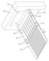
- FIG. 1 is a perspective view of the first connector of the first embodiment.
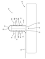
- FIG. 2 is a side view of the first connector.
- FIG. 3 is a plan view of the first connector.
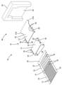
- FIG. 4 is an exploded perspective view of the first connector.
- FIG. 5 is a perspective view seen from the upper side of the second connector.
- FIG. 6 is a perspective view seen from the lower side of the second connector.
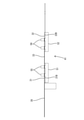
- FIG. 7 is a cross-sectional view of the second connector.
- FIG. 8 is a side view showing a state in which the first fixing portion and the second fixing portion are attached to the flexible printed substrate.
- FIG. 9 is a cross-sectional view showing a state in which the holding member is attached to the flexible printed substrate in the state shown in FIG. FIG.
- FIG. 10 is a perspective view showing a state in which the holding portion is attached to the flexible printed substrate in the state shown in FIG.
- FIG. 11 is a cross-sectional view of the first connector produced by bending the flexible printed circuit board shown in FIGS. 9 and 10.
- FIG. 12 is a perspective view showing a state in which the first connector is assembled to the second connector.
- FIG. 13 is a cross-sectional view showing a state in which the first connector is assembled to the second connector.
- connection structure of the flexible printed circuit board of the present disclosure is (1) A flexible printed board connection structure in which a flexible printed board is connected to a mating connector, wherein the flexible printed board is provided with a plurality of first contacts arranged along a predetermined first direction on the surface thereof. A plurality of second contacts arranged along with the first component in a second direction orthogonal to the first direction and arranged along the first direction are provided on the surface of the first component. A plurality of the support portions having a second component and supporting the flexible printed substrate in a bent state so that the back surface of the first component and the back surface of the second component face each other.
- the first contact and the plurality of second contacts are staggered along the first direction, and the mating connectors are arranged along the first direction, the first component and the second configuration. It has a plurality of terminal fittings that sandwich the portion from both sides in the second direction and come into contact with either the first contact or the second contact.
- a first component having a plurality of first contacts arranged along the first direction on the surface, and a second component having a plurality of second contacts arranged along the first direction on the surface. Are arranged so as to line up in the second direction orthogonal to the first direction. Therefore, the size of the flexible printed substrate in the first direction can be reduced as compared with the configuration in which the total number of contacts of the first contact and the second contact are arranged along the first direction. Since the back surface of the first component and the back surface of the second component face each other, the second component and the second component are second as compared with the structure in which the first component and the second component are planar along the second direction. The size of the flexible printed substrate in the direction can be reduced. Since the plurality of first contacts and the plurality of second contacts are staggered along the first direction, the distance between adjacent contacts in the first direction is set relatively wide, and the influence of the dimensional tolerance is not easily affected.
- the support portion has a fixing portion in which the back surface of the first component portion and the back surface of the second component portion are fixed in a plane. According to this configuration, the first component and the second component can be smoothly connected by the terminal fitting of the mating connector, as compared with the configuration in which the back surface of the first component or the back surface of the second component is curved or the like. Can be pinched.
- the fixing portion is a separate body from the first fixing portion in which the back surface of the first component portion is fixed in a planar shape and the first fixing portion, and the back surface of the second component portion is in a planar shape. It is preferable to have a second fixing portion fixed to the.
- the first fixed portion in which the back surface of the first component is fixed in a plane and the second fixed portion in which the back surface of the second component is fixed in a plane are the same two-dimensional plane. Can be lined up on top. Therefore, the reflow process can be performed on the first fixed portion and the second fixed portion arranged in a plane, and the first fixed portion and the second fixed portion can be easily fixed to the flexible printed substrate.
- the first fixing portion is fixed to the back surface of the first component portion by soldering
- the second fixing portion is fixed to the back surface of the second component portion by soldering. According to this configuration, it becomes easy to fix the back surface of the first component portion and the back surface of the second component portion to the first fixing portion and the second fixing portion so as to be flat, respectively.
- the method for manufacturing a flexible printed board unit of the present disclosure is a method for manufacturing a flexible printed board unit including a flexible printed board connected to a mating connector and a support portion for supporting the flexible printed board.
- the printed substrate is aligned with the first component having a plurality of first contacts arranged along a predetermined first direction on the surface and the first component in the second direction orthogonal to the first direction.
- the support portion has a second component portion provided on the surface thereof, and the support portion is fixed to the back surface of the first component portion.
- the first fixing portion is separate from the first fixing portion and has a second fixing portion fixed to the back surface of the second component portion.
- the first fixing portion is connected to the back surface of the first component portion by reflow solder so that the first component portion is flat, and the second component portion is connected to the back surface of the second component portion so as to be flat.
- the second fixing portion is connected by reflow solder, and after the reflow processing, the first fixing portion and the second fixing portion are connected so that the back surface of the first component portion and the back surface of the second component portion face each other. Bring it closer and bend the flexible printed substrate.
- the back surface of the first component is fixed in a plane and the back surface of the second component is fixed in a plane with respect to the flexible printed substrate in a plane.
- the fixed portion and the fixed portion can be arranged on the same two-dimensional plane. Therefore, the reflow process can be performed on the first fixed portion and the second fixed portion arranged in a plane, and the first fixed portion and the second fixed portion can be easily fixed to the flexible printed substrate. After the reflow process, the flexible printed substrate can be easily bent by bringing the first fixed portion and the second fixed portion close to each other so that the back surface of the first component portion and the back surface of the second component portion face each other.
- the method for manufacturing the flexible printed substrate unit of the present disclosure also has the same effect as that described in (1) above.
- Example 1 embodying the connection structure of the flexible printed circuit board of the present disclosure will be described with reference to FIGS. 1 to 13.
- the directions appearing in FIGS. 1, 2, 6 to 8, 12 to 14 are defined as upward and downward as they are.
- the left and right sides appearing in FIGS. 1 to 14 are defined as front and back, respectively.
- the left-right direction is synonymous with the width direction, and the front and back appearing in FIGS. 1, 2, 4, 6 to 14 are defined as right and left, respectively.
- connection structure of the flexible printed circuit board of the first embodiment is composed of the first connector 10 (flexible printed circuit board unit) shown in FIG. 1 and the second connector (counterpart connector) 60 shown in FIG.
- the first connector 10 is assembled to the second connector 60 as shown in FIG.
- the first connector 10 includes a flexible printed substrate 20 and a support portion 40.
- the flexible printed substrate 20 is supported in a bent state by the support portion 40.
- the flexible printed substrate 20 has a plurality of strip-shaped electric wires 21 and an insulating sheet 22 that covers each electric wire 21.
- the electric wire 21 is formed by, for example, gold plating.
- the electric wires 21 are arranged in parallel at a constant pitch.
- the insulating sheet 22 is a sheet made of an insulating resin.
- the electric wire 21 is covered with an insulating sheet 22.
- the flexible printed substrate 20 has a first component portion 31, a second component unit 32, a bent portion 33, and a main body portion 34.
- the first component 31, the second component 32, and the bent portion 33 form a terminal portion of the strip-shaped flexible printed circuit board 20.
- the flexible printed substrate 20 is arranged in the order of the first component portion 31, the bent portion 33, and the second component portion 32 from the main body portion 34 toward the end portion.
- the first component 31 has a flat plate shape as shown in FIGS. 1 and 2.
- the first component 31 extends upward from the end of the main body 34.
- the plate surface of the first component 31 is orthogonal to the plate surface of the main body 34.
- the connecting portion between the first component portion 31 and the main body portion 34 is curved.
- a plurality of first contacts 35 arranged at equal intervals along a predetermined first direction (left-right direction) are provided on the surface (upper surface) 31A of the first component 31.
- the first direction is the lateral direction of the insulating sheet 22.
- the first contact 35 has a rectangular shape.
- the first contact 35 is provided at the end of the electric wire 21.
- the width dimension of the first contact 35 is larger than the width dimension of the electric wire 21.
- the first contact 35 is exposed without being covered with the insulating sheet 22.
- the second component 32 has a flat plate shape as shown in FIGS. 1 and 2.
- the second component 32 extends downward from the end of the bent portion 33 (the end opposite to the first component 31), which will be described later.
- the plate surface of the second component 32 is orthogonal to the plate surface of the main body 34.
- a plurality of second contacts 36 arranged at equal intervals along the first direction (left-right direction) are provided on the surface (upper surface) 32A of the second component 32.
- the second contact 36 has a rectangular shape.
- the second contact 36 is provided at the end of the electric wire 21.
- a part of the electric wire 21 connected to the second contact 36 is also included in the first component portion 31 and the bent portion 33.
- the width dimension of the second contact 36 is the same width dimension as that of the first contact 35, that is, the width dimension of the second contact 36 is larger than the width dimension of the electric wire 21.
- the second contact 36 is exposed without being covered with the insulating sheet 22.
- the bent portion 33 connects the first constituent portion 31 and the second constituent portion 32.
- the bent portion 33 has a configuration in which the bent portion 33 is bent so as to be folded upward so as to be convex upward.
- the flexible printed substrate 20 has a plurality of first contacts 35 and a plurality of second contacts 36 in a staggered arrangement along the left-right direction in a state (planar shape) before bending. ..
- the left-right rows of the plurality of first contacts 35 and the left-right rows of the plurality of second contacts 36 are arranged so as to be offset in the front-rear direction.
- the support portion 40 supports the flexible printed substrate 20 in a bent state so that the back surface 31B of the first component unit 31 and the back surface 32B of the second component unit 32 face each other.
- the support portion 40 has a fixing portion 41 and a holding portion 42.
- the fixing portion 41 includes a first fixing portion 51 and a second fixing portion 52.
- the first fixed portion 51 and the second fixed portion 52 are separate bodies.
- the first fixing portion 51 and the second fixing portion 52 are made of, for example, metal.
- the first fixing portion 51 includes a plate portion 53, a pair of bent portions 54, four protrusions 55, and a pair of hooking portions 56.
- the plate portion 53 has a rectangular shape that is long in the left-right direction.
- the bent portion 54 is provided at the left and right edge portions of the plate portion 53, except for the hook portion 56, which will be described later.
- the bent portion 54 is bent in a U shape when viewed from the front-rear direction so as to be convex downward.
- the pair of protrusions 55 project upward in a strip shape from the tip of the bent portion 54 (the end opposite to the plate portion 53).
- the pair of hooking portions 56 project downward from the front ends of the left and right edges of the plate portion 53.
- the hooking portion 56 has a strip-like shape, and its tip is bent inward (on the other hooking portion 56 side) like a hook.
- the first fixing portion 51 is fixed to the back surface (lower surface) 31B of the first component portion 31 by soldering. As shown in FIG. 2, the back surface (lower surface) 31B of the first component 31 is fixed to the first fixing portion 51 in a planar shape.
- the upper surface (left side surface in FIG. 2) of the plate portion 53 is covered with the back surface (lower surface) 31B of the first component portion 31.
- the upper surface of the plate portion 53 is in contact with the back surface (lower surface) 31B of the first component portion 31.
- the protrusion 55 is inserted into a hole (not shown) provided in the first component 31 and is solder-connected.
- the second fixing portion 52 includes a plate portion 57, a pair of bent portions 58, and four protrusions 59.
- the plate portion 57 has a rectangular shape that is long in the left-right direction. As shown in FIG. 11, the plate portion 57 is bent into an L shape when viewed from the left-right direction. At the rear end of the plate portion 57, a pair of extending portions 57A extending on both the left and right sides are provided. The rear end side (the portion orthogonal to the front end side) of the plate portion 57 is fixed to the holding portion 42 described later. As shown in FIG. 4, the bent portion 58 is provided on the left and right edges of the plate portion 57.
- the bent portion 58 is bent in a U shape when viewed from the front-rear direction so as to be convex downward.
- the pair of protrusions 59 project upward in a strip shape from the tip of the bent portion 58 (the end opposite to the plate portion 57).
- the second fixing portion 52 is fixed to the back surface (lower surface) 32B of the second component portion 32 by soldering. As shown in FIG. 2, the back surface (lower surface) 32B of the second component 32 is fixed to the second fixing portion 52 in a planar shape.
- the upper surface (right side surface in FIG. 2) of the plate portion 57 is covered with the back surface (lower surface) 32B of the second component portion 32.
- the upper surface of the plate portion 57 is in contact with the back surface (lower surface) 32B of the second component portion 32.
- the protrusion 59 is inserted into a hole (not shown) provided near the left-right end of the second component 32, and is solder-connected.
- the holding portion 42 shown in FIG. 4 is a member that supports the fixing portion 41.
- the holding portion 42 is made of, for example, resin.
- the holding portion 42 has a rectangular parallelepiped shape.
- the holding portion 42 is provided with a groove portion 43 in which the front side and the upper side are open. A portion on the rear end side of the plate portion 57 is fixed to the bottom portion of the groove portion 43.
- Slits 44 along the front-rear direction are provided at both left and right ends of the bottom of the groove 43.
- the second fixing portion 52 is fixed to the holding portion 42 by inserting the extending portion 57A into the slit 44.
- the support portion 40 supports the flexible printed substrate 20 in a bent state so that the back surface 31B of the first component unit 31 and the back surface 32B of the second component unit 32 face each other.
- the back surface 31B of the first component 31 and the back surface 32B of the second component 32 are in contact with each other.
- the bent portion 54 and the bent portion 58 are in contact with each other along the vertical direction.
- the hooking portion 56 of the first constituent portion 31 is hooked on the left-right end portion of the plate portion 57 of the second constituent portion 32.
- the back surface 31B of the first component 31 and the back surface 32B of the second component 32 are maintained in a facing state.
- the plate surface of the plate portion 53 of the first component portion 31 and the plate surface of the plate portion 57 of the second component portion 32 are parallel to each other.
- the surface 31A of the first component 31 and the surface 32A of the second component 32 are parallel to each other.
- a plurality of first contacts 35 and a plurality of second contacts 36 are arranged alternately in the left-right direction and staggered in the front-rear direction. None.
- the rows of the plurality of first contacts 35 and the rows of the plurality of second contacts 36 are arranged so as to be offset in the front-rear direction.
- the second contact 36 is located at the center position (half the pitch) between the first contacts 35. ..
- the plurality of first contacts 35 and the plurality of second contacts 36 are arranged in a row at equal intervals in the left-right direction.
- the first connector 10 has the same number of contacts (the number of contacts in which the first contact 35 and the second contact 36 are combined) arranged along the left-right direction due to the staggered arrangement of the contacts in the left-right direction.
- the size of the flexible printed substrate 20 in the above can be reduced. Since the first connector 10 has a configuration in which the back surface 31B of the first configuration unit 31 and the back surface 32B of the second configuration unit 32 face each other, the first configuration unit 31 and the second configuration unit 32 are aligned in the front-rear direction.
- the size of the flexible printed substrate 20 in the front-rear direction can be reduced as compared with the flat configuration.
- the distance between adjacent contacts in the left-right direction between adjacent first contacts 35 and adjacent second contacts 36
- the second connector 60 includes a plurality of terminal fittings 61 and a case 62.
- the terminal fitting 61 is a tuning fork-shaped plate-shaped terminal.
- the terminal fitting 61 has a pair of holding pieces 63 and a connecting piece 64.
- the pair of holding pieces 63 project downward in parallel.
- a third contact 65 projecting inward (on the other holding piece 63 side) is provided.
- the connecting piece 64 projects in a direction orthogonal to the projecting direction of the sandwiching piece 63 on the base end side of the pair of sandwiching pieces 63.
- the connection piece 64 is exposed from the upper end of the case 62. Wiring or the like is connected to the connection piece 64, for example.
- Case 62 is open downward as shown in FIG. As shown in FIG. 7, the front and rear lower ends of the case 62 are tapered inwardly.
- the case 62 holds a plurality of terminal fittings 61.
- the plurality of terminal fittings 61 are arranged at equal intervals in the plate thickness direction.
- the protruding directions of the connection pieces 64 are opposite between the adjacent terminal fittings 61.
- the connection pieces 64 of the plurality of terminal fittings 61 are arranged in a staggered manner (see FIG. 5) along the horizontal direction.
- the row of connecting pieces 64 protruding to the front side and the row of connecting pieces 64 protruding to the rear side are arranged so as to be offset in the left-right direction.
- connection piece 64 protruding to the rear side When viewed through a plurality of terminal fittings 61 from the front-rear direction, the connection piece 64 protruding to the rear side is located at the center position (half the pitch) between the connection pieces 64 protruding to the front side. positioned.
- the connection piece 64 projecting to the front side and the connection piece 64 projecting to the rear side are arranged in a row at equal intervals in the left-right direction.
- Each terminal fitting 61 contacts either the first contact 35 or the second contact 36.
- the fixing portion 41 is attached to the flat flexible printed substrate 20.
- the first fixing portion 51 is connected to the back surface 31B of the first constituent portion 31 with reflow solder (solder paste before heat treatment) so that the first constituent portion 31 becomes flat.
- the protrusion 55 is inserted into a hole (not shown) provided in the first component 31, and reflow solder is applied.
- the second fixing portion 52 is connected to the back surface 32B of the second constituent portion 32 by reflow soldering so that the second constituent portion 32 becomes flat.
- the protrusion 59 is inserted into a hole (not shown) provided in the second component 32, and reflow solder is applied.
- first fixing portion 51 is soldered to the back surface 31B of the first configuration portion 31, and the second fixing portion 52 is soldered to the back surface 32B of the second configuration portion 32. Since the first fixing portion 51 and the second fixing portion 52 are separate bodies, the first fixing portion 51 in which the first component 31 is fixed in a plane and the second component 32 are fixed in a plane. 2 The fixing portion 52 and the fixing portion 52 can be arranged in a plane. Therefore, the first component unit 31 and the second component unit 32 can be easily reflowed.
- the second fixing portion 52 is fixed to the holding portion 42.
- the portion of the second fixing portion 52 on the rear end side of the plate portion 57 is fixed to the bottom portion of the groove portion 43.
- a structure for hooking the plate portion 57 to the groove portion 43 is provided.
- the first fixing portion 51 and the second fixing portion 52 are brought close to each other so that the back surface 31B of the first component unit 31 and the back surface 32B of the second component unit 32 face each other.
- Bend the flexible printed circuit board 20 The flexible printed circuit board 20 is bent so that the bent portion 33 is convex upward.
- the plate surface of the plate portion 53 of the first fixing portion 51 and the plate surface of the plate portion 57 of the second fixing portion 52 face each other.
- the bent portion 54 of the first fixing portion 51 and the bent portion 58 of the second fixing portion 52 come into contact with each other in the front-rear direction.
- the plate portion 53 of the first fixing portion 51 and the plate portion 57 of the second fixing portion 52 are parallel to each other in the vertical direction.
- the plate surface of the first component portion 31 and the plate surface of the second component unit 32 are parallel to each other in the vertical direction.
- the hooking portion 56 of the first constituent portion 31 is hooked on the end portion of the plate portion 57 of the second constituent portion 32 in the left-right direction.
- the back surface 31B of the first component 31 and the back surface 32B of the second component 32 are maintained in a facing state. In this way, the first connector is manufactured.
- the first connector 10 is assembled to the second connector 60.
- a closing portion 45 is provided which covers the groove portion 43 of the holding portion 42 from the upper side.
- the bent portion (first component 31, second component 32, and bent 33) of the flexible printed substrate 20 is placed inside the case 62 (more specifically, a pair of holding pieces 63). Between). The pair of holding pieces 63 of the terminal fitting 61 sandwich the first component 31 and the second component 32 from both sides in the front-rear direction.
- first component 31 and the second component 32 are fixed to the fixed portion 41 in a planar shape, a pair of components is compared with a configuration in which the first component 31 and the second component 32 have a curved shape or the like.
- the first component 31 and the second component 32 can be smoothly sandwiched by the sandwich piece 63.
- the terminal fitting 61 contacts either the first contact 35 or the second contact 36.
- the connection structure of the flexible printed substrate of the present disclosure includes a first component portion 31 on which a plurality of first contacts 35 arranged along the left-right direction (first direction) are provided on the surface, and a left-right direction (first direction).
- a plurality of second contacts 36 arranged along the first direction) are arranged so as to be aligned with the second component 32 provided on the surface in the front-rear direction (second direction) orthogonal to the left-right direction (first direction). Will be distributed. Therefore, the size of the flexible printed substrate 20 in the left-right direction (first direction) is compared with the configuration in which the total number of contacts of the first contact 35 and the second contact 36 are arranged along the left-right direction (first direction). Can be reduced.
- the first component 31 and the second component 32 are flat in the front-rear direction (second direction). It is possible to reduce the size of the flexible printed substrate 20 in the front-rear direction (second direction) as compared with the configuration in which the shape is formed. Since the plurality of first contacts 35 and the plurality of second contacts 36 form a staggered arrangement along the left-right direction (first direction), the distance between adjacent contacts in the left-right direction (first direction) is set relatively wide. Less susceptible to dimensional tolerances.
- the support portion 40 has a fixing portion 41 in which the back surface 31B of the first component portion 31 and the back surface 32B of the second component unit 32 are fixed in a plane.
- the terminal fitting 61 of the second connector (counterpart connector) 60 is the first configuration as compared with the configuration in which the back surface 31B of the first configuration unit 31 or the back surface 32B of the second configuration unit 32 has a curved shape or the like.
- the portion 31 and the second component portion 32 can be smoothly sandwiched.
- the fixing portion 41 is a separate body from the first fixing portion 51 in which the back surface 31B of the first component portion 31 is fixed in a plane shape and the first fixing portion 51. It has a second fixing portion 52 in which the back surface 32B of the second constituent portion 32 is fixed in a plane.
- the first fixing portion 51 in which the back surface 31B of the first configuration portion 31 is fixed in a plane and the second fixing portion 52 in which the back surface 32B of the second configuration portion 32 is fixed in a plane are the same. Can be lined up on a two-dimensional plane. Therefore, the reflow processing can be performed on the first fixing portion 51 and the second fixing portion 52 arranged in a plane, and the first fixing portion 51 and the second fixing portion 52 can be easily fixed to the flexible printed substrate 20. ..
- the first fixing portion 51 is fixed to the back surface 31B of the first configuration portion 31 by soldering
- the second fixing portion 52 is soldered to the back surface 32B of the second configuration portion 32. It is fixed by soldering.
- the back surface 31B of the first component 31 and the back surface 32B of the second component 32 can be easily fixed to the first fixing portion 51 and the second fixing portion 52 so as to be flat, respectively.
- the method of manufacturing the flexible printed circuit board unit of the present disclosure includes a first connector (flexible) including a flexible printed circuit board 20 connected to a second connector (mother connector) 60 and a support portion 40 for supporting the flexible printed circuit board 20. It is a manufacturing method of a printed circuit board unit) 10.
- a plurality of first contacts 35 arranged along the left-right direction are orthogonal to the first component portion 31 provided on the surface 31A in the left-right direction (first direction).
- a second component 32 provided on the surface 32A with a second contact 36 arranged alongside the first component 31 in the front-rear direction (second direction) and arranged along the left-right direction (first direction). have.
- the support portion 40 is a separate body from the first fixing portion 51 fixed to the back surface 31B of the first constituent portion 31 and the first fixing portion 51, and is fixed to the back surface 32B of the second constituent portion 32. It has a fixed portion 52 and.
- the first fixing portion 51 is connected to the flat flexible printed substrate 20 by reflow soldering to the back surface 31B of the first constituent portion 31 so that the first constituent portion 31 becomes flat.
- the second fixing portion 52 is connected to the back surface 32B of the second constituent portion 32 by reflow soldering so that the second constituent portion 32 becomes flat.
- the first fixing portion 51 and the second fixing portion 52 are brought close to each other so that the back surface 31B of the first component portion 31 and the back surface 32B of the second component portion 32 face each other, and the flexible printed substrate 20 is bent.
- the back surface 31B of the first component 31 is fixed in a plane to the flexible printed substrate 20, and the back surface 32B of the second component 32 is fixed in a plane.
- the second fixed portion 52 to be formed can be arranged on the same two-dimensional plane. Therefore, the reflow processing can be performed on the first fixing portion 51 and the second fixing portion 52 arranged in a plane, and the first fixing portion 51 and the second fixing portion 52 can be easily fixed to the flexible printed substrate 20. ..
- the flexible printed substrate 20 can be easily made by bringing the first fixing portion 51 and the second fixing portion 52 close to each other so that the back surface 31B of the first component 31 and the back surface 32B of the second component 32 face each other. Can be folded into.
- the terminal fitting 61 is a tuning fork type plate-shaped terminal, but it may have another shape.
- one contact piece (a portion in contact with either the first contact 35 or the second contact 36) may be provided.
Landscapes
- Engineering & Computer Science (AREA)
- Microelectronics & Electronic Packaging (AREA)
- Manufacturing & Machinery (AREA)
- Coupling Device And Connection With Printed Circuit (AREA)
Priority Applications (2)
| Application Number | Priority Date | Filing Date | Title |
|---|---|---|---|
| CN202180052783.6A CN115943530A (zh) | 2020-09-04 | 2021-07-30 | 柔性印制基板的连接构造及柔性印制基板单元的制造方法 |
| US18/021,948 US12362525B2 (en) | 2020-09-04 | 2021-07-30 | Connection structure for flexible printed board and method for manufacturing flexible printed board unit |
Applications Claiming Priority (2)
| Application Number | Priority Date | Filing Date | Title |
|---|---|---|---|
| JP2020148914A JP7486037B2 (ja) | 2020-09-04 | 2020-09-04 | フレキシブルプリント基板の接続構造およびフレキシブルプリント基板ユニットの製造方法 |
| JP2020-148914 | 2020-09-04 |
Publications (1)
| Publication Number | Publication Date |
|---|---|
| WO2022049945A1 true WO2022049945A1 (ja) | 2022-03-10 |
Family
ID=80491984
Family Applications (1)
| Application Number | Title | Priority Date | Filing Date |
|---|---|---|---|
| PCT/JP2021/028317 Ceased WO2022049945A1 (ja) | 2020-09-04 | 2021-07-30 | フレキシブルプリント基板の接続構造およびフレキシブルプリント基板ユニットの製造方法 |
Country Status (4)
| Country | Link |
|---|---|
| US (1) | US12362525B2 (enExample) |
| JP (1) | JP7486037B2 (enExample) |
| CN (1) | CN115943530A (enExample) |
| WO (1) | WO2022049945A1 (enExample) |
Families Citing this family (1)
| Publication number | Priority date | Publication date | Assignee | Title |
|---|---|---|---|---|
| WO2026088664A1 (ja) * | 2024-10-21 | 2026-04-30 | 株式会社村田製作所 | コネクタセット及びコネクタ |
Citations (4)
| Publication number | Priority date | Publication date | Assignee | Title |
|---|---|---|---|---|
| JPH04368787A (ja) * | 1991-06-17 | 1992-12-21 | Kel Corp | フレキシブル配線板を用いたツーピースコネクタ |
| JPH05144522A (ja) * | 1991-05-17 | 1993-06-11 | Internatl Business Mach Corp <Ibm> | モジユール・コネクタ |
| JPH09312183A (ja) * | 1996-05-23 | 1997-12-02 | Smk Corp | プリント配線基板用コネクタ |
| US6053751A (en) * | 1996-10-10 | 2000-04-25 | Thomas & Betts Corporation | Controlled impedance, high density electrical connector |
Family Cites Families (8)
| Publication number | Priority date | Publication date | Assignee | Title |
|---|---|---|---|---|
| US3158421A (en) * | 1961-12-04 | 1964-11-24 | Gen Dynamics Corp | Electrical connector for a printed circuit board and cable |
| US5044980A (en) * | 1990-01-16 | 1991-09-03 | Beta Phase, Inc. | High density and multiple insertion connector |
| US5040997A (en) * | 1990-06-08 | 1991-08-20 | The Foxboro Company | Flex circuit connector assembly and method for manufacturing the same |
| US5507651A (en) | 1991-04-22 | 1996-04-16 | Kel Corporation | Connector assembly for film circuitry |
| JP6312028B2 (ja) * | 2014-01-09 | 2018-04-18 | パナソニックIpマネジメント株式会社 | ケーブル保持部材、プラグコネクタ、コネクタ装置およびプラグコネクタの組立方法 |
| JP6090341B2 (ja) | 2015-01-09 | 2017-03-08 | 第一精工株式会社 | 電気コネクタ |
| US10219379B1 (en) * | 2017-08-07 | 2019-02-26 | Advanced Flexible Circuits Co., Ltd. | Stacked flexible printed circuit board assembly with side connection section |
| TWI759330B (zh) | 2017-09-08 | 2022-04-01 | 易鼎股份有限公司 | 可撓性電路載板的疊合插接結構 |
-
2020
- 2020-09-04 JP JP2020148914A patent/JP7486037B2/ja active Active
-
2021
- 2021-07-30 CN CN202180052783.6A patent/CN115943530A/zh active Pending
- 2021-07-30 WO PCT/JP2021/028317 patent/WO2022049945A1/ja not_active Ceased
- 2021-07-30 US US18/021,948 patent/US12362525B2/en active Active
Patent Citations (4)
| Publication number | Priority date | Publication date | Assignee | Title |
|---|---|---|---|---|
| JPH05144522A (ja) * | 1991-05-17 | 1993-06-11 | Internatl Business Mach Corp <Ibm> | モジユール・コネクタ |
| JPH04368787A (ja) * | 1991-06-17 | 1992-12-21 | Kel Corp | フレキシブル配線板を用いたツーピースコネクタ |
| JPH09312183A (ja) * | 1996-05-23 | 1997-12-02 | Smk Corp | プリント配線基板用コネクタ |
| US6053751A (en) * | 1996-10-10 | 2000-04-25 | Thomas & Betts Corporation | Controlled impedance, high density electrical connector |
Also Published As
| Publication number | Publication date |
|---|---|
| US12362525B2 (en) | 2025-07-15 |
| CN115943530A (zh) | 2023-04-07 |
| JP2022043576A (ja) | 2022-03-16 |
| US20230361516A1 (en) | 2023-11-09 |
| JP7486037B2 (ja) | 2024-05-17 |
Similar Documents
| Publication | Publication Date | Title |
|---|---|---|
| JP3300450B2 (ja) | 同軸コネクタモジュール | |
| US7811128B2 (en) | Electrical connector having improved shielding plate | |
| TW202226679A (zh) | 整體屏蔽式電纜連接器 | |
| JP4618745B1 (ja) | 電気コネクタ | |
| JPH0628791Y2 (ja) | 電気コネクタにおける端子 | |
| JP2001006771A (ja) | コネクタ | |
| JP5356621B1 (ja) | コネクタ | |
| CN111373608A (zh) | 电连接器 | |
| CN114175410B (zh) | 安全、稳固、紧凑的连接器 | |
| JP2001217025A (ja) | Pcbの終端アダプタ | |
| JP2015516109A (ja) | 印刷回路基板を相互接続するためのシステム | |
| JPH08124638A (ja) | 表面実装型コネクタ及びその電気コンタクト | |
| JP5356620B1 (ja) | コネクタ | |
| US12362525B2 (en) | Connection structure for flexible printed board and method for manufacturing flexible printed board unit | |
| CN2513243Y (zh) | 电连接器 | |
| JP2009520325A (ja) | 電気コネクタ組立体及びその製造方法 | |
| JP5622051B2 (ja) | 基板用端子およびそれを用いた基板用コネクタ | |
| TW201222992A (en) | Electrical connector and its manufacturing method | |
| CN100411255C (zh) | 使用表面贴装和插入式封装技术的印刷电路板式接头 | |
| WO2022249679A1 (ja) | コネクタおよびコネクタ実装体 | |
| JP2013125581A (ja) | 電気コネクタ | |
| JP2007242473A (ja) | 多極コネクタおよび多極コネクタの製造方法、実装方法 | |
| JP5271314B2 (ja) | 表面実装用接続端子 | |
| TWI275206B (en) | Electrical connector | |
| JP2009524906A (ja) | コネクタ |
Legal Events
| Date | Code | Title | Description |
|---|---|---|---|
| 121 | Ep: the epo has been informed by wipo that ep was designated in this application |
Ref document number: 21864003 Country of ref document: EP Kind code of ref document: A1 |
|
| NENP | Non-entry into the national phase |
Ref country code: DE |
|
| 122 | Ep: pct application non-entry in european phase |
Ref document number: 21864003 Country of ref document: EP Kind code of ref document: A1 |
|
| WWG | Wipo information: grant in national office |
Ref document number: 18021948 Country of ref document: US |