WO2022045249A1 - 熱電素子及び熱電装置 - Google Patents
熱電素子及び熱電装置 Download PDFInfo
- Publication number
- WO2022045249A1 WO2022045249A1 PCT/JP2021/031369 JP2021031369W WO2022045249A1 WO 2022045249 A1 WO2022045249 A1 WO 2022045249A1 JP 2021031369 W JP2021031369 W JP 2021031369W WO 2022045249 A1 WO2022045249 A1 WO 2022045249A1
- Authority
- WO
- WIPO (PCT)
- Prior art keywords
- thermoelectric
- thermoelectric element
- current
- magnetic field
- heat
- Prior art date
- Legal status (The legal status is an assumption and is not a legal conclusion. Google has not performed a legal analysis and makes no representation as to the accuracy of the status listed.)
- Ceased
Links
Images







Classifications
-
- H—ELECTRICITY
- H10—SEMICONDUCTOR DEVICES; ELECTRIC SOLID-STATE DEVICES NOT OTHERWISE PROVIDED FOR
- H10N—ELECTRIC SOLID-STATE DEVICES NOT OTHERWISE PROVIDED FOR
- H10N15/00—Thermoelectric devices without a junction of dissimilar materials; Thermomagnetic devices, e.g. using the Nernst-Ettingshausen effect
-
- H—ELECTRICITY
- H02—GENERATION; CONVERSION OR DISTRIBUTION OF ELECTRIC POWER
- H02N—ELECTRIC MACHINES NOT OTHERWISE PROVIDED FOR
- H02N11/00—Generators or motors not provided for elsewhere; Alleged perpetua mobilia obtained by electric or magnetic means
Definitions
- the present invention relates to a thermoelectric element and a thermoelectric device including the thermoelectric element.
- a heat pump is a device that transports heat from low temperature to high temperature.
- heat pumps that use a heat medium have been predominant, and exchange heat and transfer heat by heat of vaporization and heat of condensation.
- CFC substitutes that do not destroy the ozone layer have been used as heat media.
- the Kigali Amendment enacted in 2016 requires a significant reduction in the amount of CFC substitutes used. Therefore, there is an urgent need to develop a heat pump with a new mechanism that replaces the current mechanism that uses CFC substitutes as a heat medium.
- Non-Patent Document 1 proposes a cooling device using the Peltier effect, which is the reverse process of the Seebeck effect, as the thermoelectric effect. Further, as another thermoelectric effect, a cooling device using the Ettingshausen effect, which is the reverse process of the Nernst effect, has also been proposed (see, for example, Non-Patent Document 2 and Non-Patent Document 3). ).
- thermoelectric effect heat pumps that use the thermoelectric effect have hardly been put into practical use.
- the Pelche effect since the heat transport direction and the current are in the same direction, a three-dimensional and complicated structure in which p-type semiconductors and n-type semiconductors are alternately provided (see FIG. 3) is formed, and a large number of PN junctions are formed. I need.
- the current cooling device using the Perche effect has a low coefficient of performance (COP), which is an energy efficiency index, of about 0.5.
- COP coefficient of performance
- the present invention has been made in view of the above problems, and an object of the present invention is to provide an energy-efficient thermoelectric element and thermoelectric device using the Ettingshausen effect.
- thermoelectric element according to the embodiment of the present invention is made of a semi-metal or a semiconductor having a band gap of 0.5 eV or less, and when a current is passed in one direction and a magnetic field is applied in a direction orthogonal to the current, both the current and the magnetic field are applied. A temperature gradient is generated in the direction orthogonal to.
- thermoelectric device includes a plurality of thermoelectric elements each having a shape extending in one direction.
- the plurality of thermoelectric elements are arranged so that their longitudinal directions are parallel to each other, and are made of a semi-metal or a semiconductor having a band gap of 0.5 eV or less.
- a magnetic field is applied to, a temperature gradient is generated in the direction orthogonal to both the current and the magnetic field.
- thermoelectric element made of a semimetal or a semiconductor having a bandgap of 0.5 eV or less.
- thermoelectric device which concerns on 1st Embodiment. It is a perspective view which shows the arrangement of the plurality of thermoelectric elements constituting the thermoelectric device shown in FIG. 4A. It is a top view which shows the arrangement of the plurality of thermoelectric elements constituting the thermoelectric device shown in FIG. 4A. 6 is a graph showing the current dependence of the amount of heat absorbed for each temperature difference in the thermoelectric device according to the first embodiment including the thermoelectric element composed of Cd 3 As 2 .
- thermoelectric device is a graph showing the current dependence of COP for each temperature difference in the thermoelectric device according to the first embodiment including the thermoelectric element composed of Cd 3 As 2 .
- thermoelectric device which concerns on 2nd Embodiment.
- thermoelectric device which concerns on 3rd Embodiment.
- thermoelectric device which concerns on 3rd Embodiment.
- shape of the thermoelectric element which concerns on the modification of 3rd Embodiment.
- thermoelectric element 6 is a graph showing the relationship between (width of heat dissipation surface) / (width of cooling surface) and maximum temperature difference for the thermoelectric element shown in FIG. 10. It is a graph showing the relationship between the dimensionless figure of merit and the Carnot efficiency for each conventional Pelche element and each thermoelectric element according to each embodiment (new technology).
- the Nernst effect is a phenomenon in which when a heat flow flows through a thermoelectric element, an electromotive force is generated in a direction perpendicular to both the heat flow and the magnetization of the thermoelectric element.
- a heat flow ⁇ temperature difference ⁇ T
- the carrier is subjected to magnetization M in the width direction of the thermoelectric element.
- the direction of movement is bent, and an electromotive force V is generated in a direction perpendicular to both the magnetization M and the heat flow.
- the electromotive force V is SN ⁇ T (l / t).
- the electromotive force V generated by the Nernst effect is proportional to the shape factor l / t of the thermoelectric element.
- the Zeebeck effect is a phenomenon in which when a heat flow flows through a thermoelectric element, carriers move along the heat flow and an electromotive force is generated in the heat flow direction.
- a heat flow ⁇ temperature difference ⁇ T
- a heat flow ⁇ temperature difference ⁇ T
- an electromotive force V is generated in parallel with the heat flow.
- the Seebeck coefficient of the thermoelectric element is S
- the electromotive force V is S ⁇ T.
- FIG. 3 shows a schematic configuration of the conventional Pelche cooling device 1.
- the Pelche cooling device 1 rod-shaped p-type semiconductors 5p and n-type semiconductors 5n are alternately connected between two insulating substrates 3a and 3b, and the adjacent p-type semiconductors 5p and n-type semiconductors 5n are It is joined by a metal electrode 7.
- a current I flows in the ⁇ z direction in the n-type semiconductor 5n and in the + z direction in the p-type semiconductor 5p, heat moves in the + z direction, and heat is absorbed by the electrode on the substrate 3a side.
- Dissipation occurs at the electrode on the substrate 3b side. In this way, heat is transported from the endothermic side (cold) to the heat dissipation side (hot).
- Th be the heat dissipation side temperature
- T c be the endothermic side temperature
- R be the resistance of a pair of adjacent p-type and n-type semiconductors (hereinafter referred to as Pelche elements)
- K be the thermal conductance
- S be the Zeebeck coefficient.
- the heat dissipation amount Q h on the high temperature side and the endothermic amount Q c on the low temperature side of the Pelche element are expressed as equations (1) and (2), respectively.
- the first, second, and third terms on the right side of equations (1) and (2) represent the Perche effect, Joule heat, and heat conduction (heat inflow from high temperature), respectively.
- the width in the x direction of each of the p-type and n-type semiconductors constituting the Pelche element is w
- the depth in the y direction is l
- the thickness (height) in the z direction is t
- the electrical resistivity of the Pelche element is ⁇
- the heat Assuming that the conductivity is ⁇ , the resistivity R and the thermal conductance K of the Pelche element are expressed by the equation (3).
- each Pelche element is composed of Bi 2 Te 3
- 40 mm ⁇ 40 mm each is composed of 120 sets of Pelche elements (that is, 120 sets of p-type and n-type semiconductors) having a size of 1 mm ⁇ 1 mm ⁇ 1 mm.
- the electrical resistivity ⁇ of each Pelche element is about 103 ⁇ cm
- the thermal conductivity ⁇ is about 2 W / Km
- the Seebeck coefficient S is about 200 ⁇ V / K
- the resistance R tot thermal conductance ⁇ tot
- the coefficients Shot are about 3 ⁇ , about 0.5W / K, and about 0.05V / K, respectively.
- the total amount of heat absorbed by the entire module is expressed as Q c_tot .
- Q c_tot The total amount of heat absorbed by the entire module is expressed as Q c_tot .
- the first term (Perche effect) of the equation (2) is about in the total heat absorption Q c_tot . 14W
- the second term (Joule heat) is about 1.5W
- the third term (heat conduction) is about 1W.
- the COP max which is the maximum value of the COP of the entire module composed of the above-mentioned Pelche element, is about 4 as shown in the equation (4).
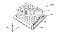
- thermoelectric device 100 shows a schematic configuration of the thermoelectric device 100 according to the first embodiment.
- the thermoelectric device 100 is a heat pump using the Ettingshausen effect, and includes a plurality of rectangular parallelepiped thermoelectric elements 104 extending in one direction (y direction). As shown in FIGS. 4A to 4C, the plurality of thermoelectric elements 104 are arranged in parallel on the substrate 102 in a direction perpendicular to the longitudinal direction (x direction) so that their respective longitudinal directions (y direction) are parallel. Have been placed.
- the + y side of the thermoelectric element 104 of interest is connected to the ⁇ y side of the thermoelectric element 104 adjacent to the + x side by a copper wiring 106, and the ⁇ y side of the thermoelectric element 104 of interest is ⁇ . It is connected to the + y side of the thermoelectric element 104 adjacent to the x side by the copper wiring 106.
- the plurality of thermoelectric elements 104 are electrically connected in series so that the current I flows in the same direction (for example, the + y direction).
- the thermoelectric element 104 is made of a semimetal or a semiconductor having a bandgap of 0.5 eV or less, and has higher mobility (inversely proportional to the electrical resistivity ⁇ ) and higher thermal conductivity ⁇ than the conventional Pelche element at the operating temperature. It consists of a small material.
- the gapless semimetal include Cd 3 As 2 which is a Dirac semimetal, Ag 2 Se, and Ag 2 Te.
- the semiconductor material include InSb, Bi 0.5 Sb 1.5 Te 3 , AgCuSe, simple substance Te, Ag 8 SiSe 6 , or Ag 8 SnSe 6 .
- the Mn 3 Sn-based, Full-Whisler-based Co 2 Mn Ga, and Fe 3 Ga-based thermoelectric materials in which the inventors of the present application have observed the anomalous Nernst effect are also expected as material candidates for heat pumps using the Ettingshausen effect. can do.
- the anomalous Nernst effect of Mn 3 Sn thermoelectric materials is disclosed in Japanese Patent No. 6611167 and the following papers.
- Arabic Ikhlas, Takahiro Tomita, Takashi Koretsune, Michi-To Suzuki, Daisuke Nishio-Hamane, Ryotaro Arita, Yoshichika Otani and Satoru Nakatsuji “Large anomalous Nernst effect at room temperature in a chiral antiferromagnet.” Nature Physics volume 13, pages 1085- 1090 (2017).
- the anomalous Nernst effects of full-Whisler-based Co 2 Mn Ga and Fe 3 Ga-based thermoelectric materials are disclosed in International Publication No. 2019/009308 and PCT / JP2020 / 018010, respectively.
- a plurality of heat sinks 110 (heat sinks) made of a metal material having high thermal conductivity such as aluminum, iron, or copper are provided on the heat radiation side of the plurality of thermoelectric elements 104. Dissipate heat from the thermoelectric element 104. Although only a part of the heat sink 110 is shown in FIG. 4A, the actual heat sink 110 is provided so as to cover the entire plurality of thermoelectric elements 104. In order to improve the heat dissipation efficiency of the heat radiating plate 110, a shape having a large surface area is adopted. For example, in addition to the structure having a plurality of protrusions as shown in FIG. 4A, there is a bellows-shaped structure.
- thermoelectric element 104 When a current I is passed through the plurality of thermoelectric elements 104 in the + y direction along their respective longitudinal directions and a magnetic field H is applied in the + x direction orthogonal to the current I, each thermoelectric element 104 is magnetized in the + x direction and the current is applied. A temperature gradient is generated in the z direction orthogonal to both I and the magnetic field H, and heat is transported from the heat absorbing side (cold) to the heat dissipation side (hot) (in the + z direction).
- each thermoelectric element 104 has a width of w in the x direction, a length of l in the y direction, and a thickness of t in the z direction.
- the heat dissipation side temperature of each thermoelectric element 104 is Th
- the heat absorption side temperature is T c
- the resistance is R
- the thermal conductance is K
- the Nernst coefficient is SN
- the heat dissipation amount Q h and the heat absorption amount Q of each thermoelectric element 104.
- c is expressed as the formula (5) and the formula (6), respectively.
- the first, second, and third terms on the right side of equations (5) and (6) represent the Ettingshausen effect, Joule heat, and heat conduction (heat inflow from high temperature), respectively.
- the first term representing the Ettingshausen effect is proportional to the shape factor l / t of each thermoelectric element 104.
- thermoelectric element 104 The resistance R and the thermal conductance K of each thermoelectric element 104 are expressed by the equation (7).
- 20 thermoelectric elements 104 are arranged so that the total length l of the plurality of thermoelectric elements 104 is 0.8 m.
- the total amount of heat absorbed by the entire sample is expressed as Q c_tot .
- the electrical resistivity ⁇ of each thermoelectric element 104 is 100 ⁇ cm, the thermal conductivity ⁇ is 15 W / Km, and the Nernst coefficient SN is 200 ⁇ V / K.
- the first term (Ettingshausen effect) of 6) is about 96 W
- the second term (Joule heat) is about 1.5 W
- the third term (heat conduction) is about 24 W.
- FIG . 5 shows the current dependence of the heat absorption amount Qc when a magnetic field of 0.5 T is applied to a sample of the above size (FIG. 4C) in which each thermoelectric element 104 is made of Cd 3 As 2 for each temperature difference ⁇ T. ..
- FIG. 5 shows the current dependence of the heat absorption amount Qc when a magnetic field of 0.5 T is applied to a sample of the above size (FIG. 4C) in which each thermoelectric element 104 is made of Cd 3 As 2 for each temperature difference ⁇ T. ..
- FIG. 5 shows the current dependence of the heat absorption amount Qc when a magnetic field of 0.5 T is applied to a sample of the above size (FIG. 4C) in which each thermoelectric element 104 is made of Cd 3 As 2 for each temperature difference ⁇ T. ..
- the smaller the temperature difference ⁇ T the larger the heat absorption amount Q c
- the heat absorption amount Q c takes the maximum value when the current I is 10 A.
- thermoelectric device 100 using the Ettingshausen effect, the cooling performance of the thermoelectric device 100 can be controlled by the shape factor l / t of the thermoelectric element 104. This makes it possible to realize high conversion efficiency that could not be realized by the conventional Pelche element.
- thermoelectric elements 104 arranged so that their longitudinal directions are parallel to each other are electrically connected in series so that a current I in the same direction flows, but they are adjacent thermoelectric elements.
- a circuit configuration may be adopted in which currents flowing in opposite directions to each other flow.
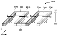
- FIG. 7 shows a schematic configuration of the thermoelectric device 200A according to the second embodiment.
- the thermoelectric device 200A includes a plurality of first thermoelectric elements 204a and a plurality of second thermoelectric elements 204b having a rectangular shape and the same size, and the respective longitudinal directions (y directions) are parallel to each other.
- the first thermoelectric element 204a and the second thermoelectric element 204b are alternately arranged.
- the first thermoelectric element 204a and the second thermoelectric element 204b are made of the same material as the thermoelectric element 104 according to the first embodiment.
- thermoelectric device 200A also absorbs heat from the plurality of first thermoelectric elements 204a and the plurality of second thermoelectric elements 204b, similarly to the thermoelectric device 100 (FIG. 4A) according to the first embodiment.
- a substrate is provided on the cold side, and a heat dissipation plate is provided on the heat dissipation side (hot).
- thermoelectric device 200B FIG. 8 described later.
- the + y side of the first thermoelectric element 204a of interest is connected to the + y side of the second thermoelectric element 204b adjacent to the + x side by a copper wiring 206, and-of the first thermoelectric element 204a of interest.
- the y side is connected to the ⁇ y side of the second thermoelectric element 204b adjacent to the ⁇ x side by the copper wiring 206.
- the plurality of thermoelectric elements are electrically connected in series so that the currents I flow in opposite directions to the adjacent thermoelectric elements due to the structure in which the + y side is connected to each other and the ⁇ y side is connected to each other alternately. It is connected to the.
- FIG. 7 shows an example in which a current I in the + y direction flows through the first thermoelectric element 204a and a current I in the ⁇ y direction flows through the second thermoelectric element 204b.
- thermoelectric element 204a Since the current I flows in the opposite directions to the first thermoelectric element 204a and the second thermoelectric element 204b, in order to generate a temperature gradient in the same direction (+ z direction or ⁇ z direction) due to the Ettingshausen effect, these It is necessary to apply magnetic currents in opposite directions to the thermoelectric element. For example, as shown in FIG. 7, assuming that the direction from the heat absorbing side (cold) to the heat radiating side (hot) is the + z direction, a magnetic field H1 in the + x direction is applied to the first thermoelectric element 204a by a permanent magnet.
- thermoelectric element 204b By applying a magnetic field H2 in the ⁇ x direction to the second thermoelectric element 204b with a permanent magnet, the first thermoelectric element 204a is magnetized in the + x direction and the second thermoelectric element 204b is magnetized in the ⁇ x direction. That is, alternating magnetic fields in opposite directions are applied to adjacent thermoelectric elements.
- thermoelectric device 200A since the plurality of first thermoelectric elements 204a and the plurality of second thermoelectric elements 204b constituting the thermoelectric device 200A are in the same plane, it is necessary to apply the alternating magnetic fields H1 and H2 in the same plane. However, it is structurally not easy to apply an alternating magnetic field in the opposite direction to adjacent thermoelectric elements in the same plane. Therefore, if the first thermoelectric element and the second thermoelectric element are arranged in separate planes, a magnetic field in the same direction can be applied in the same plane.
- thermoelectric device 200B a plurality of first thermoelectric elements 224a and a plurality of second thermoelectric elements 224b having a rectangular shape and the same size are provided, and the plurality of first thermoelectric elements 224a are provided.
- Arranged in odd-numbered stages in the + z direction (1st stage, 3rd stage, ...) and odd-numbered rows in the + x direction (1st row, 3rd row, ...), and a plurality of second thermoelectric elements 224b are even numbers in the + z direction. It may be arranged in the columns (second column, fourth column, ...) And even columns in the + x direction (second column, fourth column, ).
- first thermoelectric element 224a and the second thermoelectric element 224b have different positions in the first direction (z direction) perpendicular to the longitudinal direction (y direction), and are perpendicular to both the longitudinal direction and the first direction.
- the positions in the two directions (x direction) are also arranged so as to be different from each other.
- the first thermoelectric element 224a and the second thermoelectric element 224b are also made of the same material as the thermoelectric element 104 according to the first embodiment.
- thermoelectric element 224a Currents in opposite directions flow along the longitudinal direction in the first thermoelectric element 224a and the second thermoelectric element 224b.
- the current I flows in the + y direction in the first thermoelectric element 224a
- the current I flows in the ⁇ y direction in the second thermoelectric element 224b.
- thermoelectric element 224a In order to generate a temperature gradient in the same direction (+ z direction or ⁇ z direction) due to the Ettingshausen effect, it is necessary to apply magnetic fields in opposite directions to the first thermoelectric element 224a and the second thermoelectric element 224b.
- a permanent magnet 226 having a magnetization of + x direction is arranged between two first thermoelectric elements 224a adjacent to each other in the x direction, and two second thermoelectric elements 224b adjacent to each other in the x direction.
- a permanent magnet 226 whose magnetization is in the ⁇ x direction may be placed between them.
- Each permanent magnet 226 is made of a material having a larger coercive force than the first thermoelectric element 224a and the second thermoelectric element 224b. Further, in order to make the thermal conductivity in the direction in which the temperature gradient occurs (z direction) uniform, it is preferable that each permanent magnet 226 is made of a material having the same thermal conductivity as the first thermoelectric element 224a and the second thermoelectric element 224b. ..
- the magnetization in the same plane is stabilized.
- Non-Patent Document 1 the cooling performance is enhanced by stacking plate-shaped blocks made of Pelche elements in the direction in which the temperature gradient is generated and forming the blocks on the heat dissipation side in a stepped shape wider than the blocks on the endothermic side. It is disclosed that it will be done.
- the loss due to a large number of PN junctions is extremely high, which causes a decrease in device performance. Therefore, as in Non-Patent Document 1, when a plurality of blocks are multiple-connected, there is a problem that the loss due to the PN junction becomes larger.
- thermoelectric elements exhibiting the Ettingshausen effect do not require a PN junction, it is considered that the element performance can be fully exhibited even if plate-shaped thermoelectric elements are stacked as described above. Therefore, in the third embodiment, a structure in which a plurality of thermoelectric elements exhibiting the Ettingshausen effect are stacked and a structure equivalent thereto will be described.
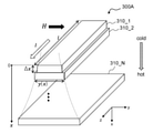
- the thermoelectric device 300A has a plurality of plate-shaped thermoelectric elements 310_1, 310_2, ..., 310_N (N is 2 or more) stacked in a direction (x direction) in which a temperature gradient is generated.
- the thermoelectric element is made of the same material as the thermoelectric element 104 according to the first embodiment.
- the number of thermoelectric elements constituting the thermoelectric device 300A is not particularly limited.
- thermoelectric elements 310_1, 310_2, ..., 310_N all have the same thickness ⁇ x in the direction in which the temperature gradient occurs (x direction) and the length l in the direction in which the current I flows (z direction; longitudinal direction).
- the widths in the direction (y direction) in which the magnetic field H is applied are different from each other. Specifically, the thermoelectric element on the heat dissipation side (hot) is wider than the thermoelectric element on the endothermic side (cold), and the cross section in the xy plane has a symmetrical staircase shape.
- thermoelectric element When a current I is passed in the + z direction along the longitudinal direction of each thermoelectric element constituting the thermoelectric device 300A and a magnetic field H is applied in the + y direction orthogonal to the current I, each thermoelectric element is magnetized in the + y direction. A temperature gradient is generated in the x direction orthogonal to both the current I and the magnetic field H, and heat is transported from the heat absorbing side (cold) to the heat dissipation side (hot) (in the + x direction).
- y (x) be the width of the thermoelectric element at this position x in the y direction.
- the electrical resistivity, thermal conductivity, and Nernst coefficient of each thermoelectric element are ⁇ , ⁇ , and SN , respectively.
- (X + ⁇ x) is expressed as Eq. (9) and Eq. (10), respectively.
- T m (x) and T m (x + ⁇ x) are the temperature on the endothermic side (x) and the temperature on the heat dissipation side (x + ⁇ x) of the m-th thermoelectric element 310_m, respectively.
- t m (x) represents the temperature gradient in the m-th thermoelectric element 310_m, and is defined as in the equation (11).
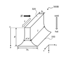
- thermoelectric element 300B in the structure in which a large number of thermoelectric elements having a small thickness ⁇ x are stacked, the direction in which the magnetic field H is applied from the endothermic side (cold) to the heat dissipation side (hot) of one thermoelectric element 300B. It is equivalent to the structure that widens the width in.
- thermoelectric element 300B for a thermoelectric element exhibiting the Ettingshausen effect, the optimum shape that brings about the maximum temperature difference is a shape in which the width increases exponentially from the endothermic side (cold) to the heat dissipation side (hot). It is shown to be. Therefore, it is considered that the thermoelectric element 300B may have such a shape.
- the thermoelectric element 300B is also made of the same material as the thermoelectric element 104 according to the first embodiment.
- the thickness of the thermoelectric element 300B is X
- the width y (x) of the thermoelectric element 300B at the position x in the direction in which the temperature gradient is generated may be defined as in the equation (12).
- FIG. 11 shows the maximum temperature difference ⁇ T max obtained when the value of y h / y c of the thermoelectric element 300B is changed.
- the Nernst coefficient SN of the thermoelectric element 300B was 200 ⁇ V / K
- the electrical resistivity ⁇ was 100 ⁇ cm
- the thermal conductivity ⁇ was 15 W / Km
- the heat dissipation side temperature Th was fixed at 300 K.
- the maximum temperature difference ⁇ T max increases as y h / y c increases. In this way, by adopting a shape in which the width y (x) increases exponentially from the endothermic side to the heat dissipation side as in equation (12) for materials with the same performance, a larger temperature difference can be obtained. It can be realized.
- each thermoelectric element according to the first to third embodiments has a simpler element structure than the Pelche element and has a degree of freedom in shape.
- the cooling performance can be further improved.
- thermoelectric element exhibiting the Ettingshausen effect according to the first to third embodiments has significantly better Carnot efficiency than the Pelche element.
Landscapes
- Cooling Or The Like Of Semiconductors Or Solid State Devices (AREA)
Abstract
エッティングスハウゼン効果を用いたエネルギー効率の良い熱電素子及び熱電装置を提供する。熱電素子104は、半金属又はバンドギャップが0.5eV以下の半導体からなり、一方向に電流Iを流し、電流Iと直交する方向に磁場Hを印加すると、電流Iと磁場Hの双方に直交する方向に温度勾配(Tc→Th)が生じる。熱電装置は、各々が一方向に延在した形状をなす複数の熱電素子104を備えており、複数の熱電素子104は、それぞれの長手方向が平行になるように基板102に配置されている。
Description
本発明は、熱電素子、及び熱電素子を備えた熱電装置に関する。
ヒートポンプは、低温から高温へ熱を輸送するデバイスである。ヒートポンプは、これまで熱媒体を用いたものが支配的であり、気化熱及び凝縮熱による熱のやり取りと熱輸送を行う。近年、オゾン層を破壊しない代替フロンが熱媒体として用いられてきた。しかしながら、代替フロンはCO2に比べてはるかに温室効果が高いため、2016年に制定されたキガリ改正(Kigali Amendment)により、代替フロンの使用量の大幅な削減が求められている。したがって、現行の代替フロンを熱媒体とした機構に代わる新たな仕組みのヒートポンプの開発が急務である。
ヒートポンプに熱電効果を用いる研究が1950年代から続けられている。例えば、非特許文献1では、熱電効果として、ゼーベック効果(Seebeck effect)の逆過程であるペルチェ効果(Peltier effect)を用いた冷却装置が提案されている。また、別の熱電効果として、ネルンスト効果(Nernst effect)の逆過程であるエッティングスハウゼン効果(Ettingshausen Effect)を用いた冷却装置も提案されている(例えば、非特許文献2及び非特許文献3参照)。
T. Metzger, R.P. Huebener,"Modelling and cooling behaviour of Peltier cascades," Cryogenics, Volume 39, 1999, Pages 235-239.
B. J. O'Brien and C. S. Wallace, "Ettingshausen Effect and Thermomagnetic Cooling," Journal of Applied Physics 29, 1958, Pages 1010-1012.
R. T. Delves. "The prospects for Ettingshausen and Peltier cooling at low temperatures," British Journal of Applied Physics, Volume 13, 1962, Pages 440-445.
しかしながら、熱電効果を用いたヒートポンプは、ほとんど実用化に至っていない。特に、ペルチェ効果では、熱の輸送方向と電流が同じ方向であるため、p型半導体とn型半導体とを交互に設けた立体的で複雑な構造(図3参照)となり、多数のPN接合を必要とする。これにより、ペルチェ効果を用いた現状の冷却装置は、エネルギー効率指標である成績係数(Coefficient Of Performance:COP)が0.5程度の低い値となっている。
本発明は、上記課題に鑑みてなされたものであり、エッティングスハウゼン効果を用いたエネルギー効率の良い熱電素子及び熱電装置を提供することを目的とする。
本発明の一実施形態に係る熱電素子は、半金属又はバンドギャップが0.5eV以下の半導体からなり、一方向に電流を流し、電流と直交する方向に磁場を印加すると、電流と磁場の双方に直交する方向に温度勾配が生じる。
本発明の一実施形態に係る熱電装置は、各々が一方向に延在した形状をなす複数の熱電素子を備える。複数の熱電素子は、それぞれの長手方向が平行になるように配置され、半金属又はバンドギャップが0.5eV以下の半導体からなり、それぞれの長手方向に沿った電流を流し、電流と直交する方向に磁場を印加すると、電流と磁場の双方に直交する方向に温度勾配が生じる。
本発明によれば、半金属又はバンドギャップが0.5eV以下の半導体からなる熱電素子がエッティングスハウゼン効果を示すことにより、エネルギー効率を向上させることが可能となる。
以下、添付の図面を参照して、本発明の例示の実施形態について説明する。
図面において、同一又は同様の構成要素には同一の参照符号を付している。図面は模式的なものであり、平面寸法と厚みとの関係、及び各部材の厚みの比率は現実のものとは異なる。また、図面相互間においても互いの寸法の関係や比率が異なる部分が含まれていることは勿論である。
図面において、同一又は同様の構成要素には同一の参照符号を付している。図面は模式的なものであり、平面寸法と厚みとの関係、及び各部材の厚みの比率は現実のものとは異なる。また、図面相互間においても互いの寸法の関係や比率が異なる部分が含まれていることは勿論である。
まず、図1及び図2を参照して、ネルンスト効果及びゼーベック効果についてそれぞれ説明する。
ネルンスト効果とは、熱電素子に熱流が流れると、熱流及び熱電素子の磁化の双方に垂直な方向に起電力が生じる現象である。例えば、図1に示すように、直方体状の熱電素子(奥行l、幅w、厚みt)において厚み方向に熱流(∝温度差ΔT)が流れると、熱電素子の幅方向における磁化Mによりキャリアの移動方向が曲げられ、磁化Mと熱流の双方に垂直な方向に起電力Vが生じる。熱電素子のネルンスト係数をSNとすると、起電力VはSNΔT(l/t)である。このように、ネルンスト効果により発生する起電力Vは、熱電素子の形状因子l/tに比例する。
一方、ゼーベック効果とは、熱電素子に熱流が流れると、キャリアが熱流に沿って移動し、熱流方向に起電力が生じる現象である。例えば、図2に示すように、直方体状の熱電素子(奥行l、幅w、厚みt)において厚み方向に熱流(∝温度差ΔT)が流れると、熱流に平行に起電力Vが生じる。熱電素子のゼーベック係数をSとすると、起電力VはSΔTである。
次に、ゼーベック効果の逆過程であるペルチェ効果を用いた従来のヒートポンプ(以下、ペルチェ冷却装置と呼ぶ。)の機構について説明する。
図3に、従来のペルチェ冷却装置1の概略構成を示す。ペルチェ冷却装置1は、2枚の絶縁性基板3a及び3bの間に、棒状のp型半導体5pとn型半導体5nとが交互に連結され、隣接するp型半導体5pとn型半導体5nとは金属電極7で接合されている。図3に示すように直流電圧Vをかけると、n型半導体5nでは-z方向、p型半導体5pでは+z方向に電流Iが流れ、+z方向に熱が移動し、基板3a側の電極において吸熱、基板3b側の電極において放熱が起こる。このようにして、吸熱側(cold)から放熱側(hot)へ熱が輸送される。
放熱側温度をTh、吸熱側温度をTcとし、一対の隣接するp型及びn型半導体(以下、ペルチェ素子と呼ぶ。)の抵抗をR、熱コンダクタンスをK、ゼーベック係数をSとすると、ペルチェ素子の高温側の放熱量Qh及び低温側の吸熱量Qcは、それぞれ、式(1)及び式(2)のように表される。

式(1)及び式(2)の右辺第1項、第2項、及び第3項は、それぞれ、ペルチェ効果、ジュール熱、及び熱伝導(高温からの熱流入)を表している。
ペルチェ素子を構成するp型及びn型半導体の各々のx方向における幅をw、y方向における奥行をl、z方向における厚み(高さ)をtとし、ペルチェ素子の電気抵抗率をρ、熱伝導度をκとすると、ペルチェ素子の抵抗R及び熱コンダクタンスKは、式(3)のように表される。

例えば、各ペルチェ素子がBi2Te3からなるものとし、1つあたり1mm×1mm×1mmのサイズのペルチェ素子120組(すなわち、120組のp型及びn型半導体)から構成される40mm×40mm×4mmのサイズのモジュールを用意する。各ペルチェ素子の電気抵抗率ρを約103μΩcm、熱伝導度κを約2W/Km、ゼーベック係数Sを約200μV/Kとすると、モジュール全体での抵抗Rtot、熱コンダクタンスΚtot、及びゼーベック係数Stotは、それぞれ、約3Ω、約0.5W/K、約0.05V/Kとなる。
モジュール全体での全吸熱量をQc_totと表記する。モジュールに1Aの電流Iを流し、生じた温度差ΔT(=Th-Tc)を2℃とすると、全吸熱量Qc_totのうち、式(2)の第1項(ペルチェ効果)は約14W、第2項(ジュール熱)は約1.5W、第3項(熱伝導)は約1Wとなる。
上述のペルチェ素子からなるモジュール全体のCOPの最大値であるCOPmaxは、式(4)に示すように約4となる。

このように、ペルチェ冷却装置1は多数のPN接合を設ける必要があるため、COPが低く、素子性能の低下を招いていることがわかる。また、電流I又は温度差ΔT(=Th-Tc)が大きくなると、COPが大きく減少することがわかる。なお、上述のように、現状のペルチェ冷却装置は、COPが0.5程度である。
次に、図4A~図12を参照して、ネルンスト効果の逆過程であるエッティングスハウゼン効果を用いた本発明の第1、第2及び第3実施形態を説明する。
<第1実施形態>
まず、図4A~図6を参照して、本発明の第1実施形態を説明する。図4A~図4Cに、第1実施形態に係る熱電装置100の概略構成を示す。
まず、図4A~図6を参照して、本発明の第1実施形態を説明する。図4A~図4Cに、第1実施形態に係る熱電装置100の概略構成を示す。
熱電装置100は、エッティングスハウゼン効果を用いたヒートポンプであり、一方向(y方向)に延在した直方体状の熱電素子104を複数備える。図4A~図4Cに示すように、複数の熱電素子104は、基板102上に、それぞれの長手方向(y方向)が平行になるように、長手方向と垂直な方向(x方向)に並列に配置されている。
図4Cに示すように、着目する熱電素子104の+y側は、+x側に隣接する熱電素子104の-y側と銅配線106によって接続され、当該着目する熱電素子104の-y側は、-x側に隣接する熱電素子104の+y側と銅配線106によって接続される。このように、複数の熱電素子104は、同じ向き(例えば+y方向)に電流Iが流れるように、電気的に直列に接続されている。
熱電素子104は、半金属又はバンドギャップが0.5eV以下の半導体からなり、使用温度において、従来のペルチェ素子よりも、移動度(電気抵抗率ρに反比例する。)が高く熱伝導度κが小さい材料からなる。ギャップレスの半金属としては、ディラック半金属(Dirac semimetal)であるCd3As2の他、Ag2Se、Ag2Teなどが挙げられる。半導体材料としては、InSb、Bi0.5Sb1.5Te3、AgCuSe、単体のTe、Ag8SiSe6、又はAg8SnSe6などが挙げられる。
その他、本願発明者らが異常ネルンスト効果を観測した、Mn3Sn系、フルホイスラー系Co2MnGa、及びFe3Ga系の熱電材料についても、エッティングスハウゼン効果を用いたヒートポンプの材料候補として期待することができる。
Mn3Sn系の熱電材料の異常ネルンスト効果については、日本国特許第6611167号及び以下の論文に開示されている。
Muhammad Ikhlas, Takahiro Tomita, Takashi Koretsune, Michi-To Suzuki, Daisuke Nishio-Hamane, Ryotaro Arita, Yoshichika Otani and Satoru Nakatsuji, “Large anomalous Nernst effect at room temperature in a chiral antiferromagnet.” Nature Physics volume 13, pages 1085-1090 (2017).
フルホイスラー系Co2MnGa、Fe3Ga系熱電材料の異常ネルンスト効果については、それぞれ、国際公開第2019/009308号、PCT/JP2020/018010に開示されている。
Muhammad Ikhlas, Takahiro Tomita, Takashi Koretsune, Michi-To Suzuki, Daisuke Nishio-Hamane, Ryotaro Arita, Yoshichika Otani and Satoru Nakatsuji, “Large anomalous Nernst effect at room temperature in a chiral antiferromagnet.” Nature Physics volume 13, pages 1085-1090 (2017).
フルホイスラー系Co2MnGa、Fe3Ga系熱電材料の異常ネルンスト効果については、それぞれ、国際公開第2019/009308号、PCT/JP2020/018010に開示されている。
図4Aに示すように、複数の熱電素子104の放熱側には、アルミニウム、鉄、又は銅などの高い熱伝導性を有する金属材料からなる放熱板110(ヒートシンク)が設けられており、複数の熱電素子104からの熱を放出する。図4Aでは、放熱板110の一部のみを示しているが、実際の放熱板110は、複数の熱電素子104全体を覆うように設けられている。放熱板110の放熱効率を向上させるため、表面積が広くなるような形状が採用されており、例えば、図4Aのような複数の突起部を有する構造の他、蛇腹状の構造のものがある。
複数の熱電素子104に、例えば、それぞれの長手方向に沿った+y方向に電流Iを流し、電流Iと直交する+x方向に磁場Hを印加すると、各熱電素子104は+x方向に磁化され、電流Iと磁場Hの双方に直交するz方向に温度勾配が生じ、吸熱側(cold)から放熱側(hot)へ(+z方向へ)熱が輸送される。
各熱電素子104は、図4Bに示すように、x方向における幅がw、y方向における長さがl、z方向における厚みがtであるものとする。各熱電素子104の放熱側温度をTh、吸熱側温度をTcとし、抵抗をR、熱コンダクタンスをK、ネルンスト係数をSNとすると、各熱電素子104の放熱量Qh及び吸熱量Qcは、それぞれ、式(5)及び式(6)のように表される。

式(5)及び式(6)の右辺第1項、第2項、及び第3項は、それぞれ、エッティングスハウゼン効果、ジュール熱、及び熱伝導(高温からの熱流入)を表している。エッティングスハウゼン効果を表す第1項は、各熱電素子104の形状因子l/tに比例している。
各熱電素子104の抵抗R及び熱コンダクタンスKは、式(7)のように表される。

図4Cに示すように、サイズが50mm×50mmの基板102の40mm×40mmの領域に、厚さt=0.5mm、幅w=0.5mm、長さl=40mmの複数の熱電素子104を平行に並べた試料を用意する。ここでは、複数の熱電素子104の長さlの合計が0.8mとなるように、20個の熱電素子104が配置されるものとする。
試料全体での全吸熱量をQc_totと表記する。各熱電素子104の電気抵抗率ρを100μΩcm、熱伝導度κを15W/Km、ネルンスト係数SNを200μV/Kとする。試料に0.5Tの磁場Hを印加し、1Aの電流Iを流したときに生じた温度差ΔT(=Th-Tc)を2℃とすると、全吸熱量Qc_totのうち、式(6)の第1項(エッティングスハウゼン効果)は約96W、第2項(ジュール熱)は約1.5W、第3項(熱伝導)は約24Wとなる。試料全体の抵抗をRtotと表記すると、試料全体のCOPは、式(8)に示すように約15という大きな値をとる。

図5に、各熱電素子104がCd3As2からなる上述のサイズの試料(図4C)に0.5Tの磁場を印加したときの吸熱量Qcの電流依存性を温度差ΔTごとに示す。図5に示すように、同じ電流Iに対し、温度差ΔTが小さいほど吸熱量Qcが大きくなる一方で、温度差ΔTが大きいほど吸熱量Qcが小さくなり、低温から高温への熱輸送が困難になることがわかる。また、同じ温度差ΔTでも電流Iが10Aときに吸熱量Qcが最大値をとることがわかる。この試料では最大で約70℃の温度差をつけられる。
この試料について、図6に、COPの電流依存性を温度差ΔTごとに示す。図6に示すように、温度差ΔTが小さいほどCOPが高くなり、ΔT=1Kでは、COPが30を超えることがわかる。
以上のように、エッティングスハウゼン効果を用いた熱電装置100によると、熱電素子104の形状因子l/tによって熱電装置100の冷却性能をコントロールすることができる。これにより、従来のペルチェ素子では実現できなかった高変換効率を実現することが可能となる。
<第2実施形態>
次に、図7及び図8を参照して、本発明の第2実施形態を説明する。
次に、図7及び図8を参照して、本発明の第2実施形態を説明する。
第1実施形態では、それぞれの長手方向が平行になるように配置された複数の熱電素子104は、同じ向きの電流Iが流れるように電気的に直列に接続されていたが、隣接する熱電素子に互いに逆向きの電流が流れるような回路構成を採用してもよい。
図7に、第2実施形態に係る熱電装置200Aの概略構成を示す。熱電装置200Aは、図7に示すように、直方体状で同一サイズの複数の第1熱電素子204aと複数の第2熱電素子204bとを備え、それぞれの長手方向(y方向)が平行になるように、第1熱電素子204aと第2熱電素子204bが交互に配置されている。第1熱電素子204a及び第2熱電素子204bは、第1実施形態に係る熱電素子104と同じ材料からなる。
なお、図7には示していないが、熱電装置200Aも、第1実施形態に係る熱電装置100(図4A)と同様に、複数の第1熱電素子204aと複数の第2熱電素子204bの吸熱側(cold)に基板を備え、放熱側(hot)に放熱板を備えている。後述の熱電装置200B(図8)についても同様である。
図7に示すように、着目する第1熱電素子204aの+y側は、+x側に隣接する第2熱電素子204bの+y側と銅配線206によって接続され、当該着目する第1熱電素子204aの-y側は、-x側に隣接する第2熱電素子204bの-y側と銅配線206によって接続される。このように、複数の熱電素子は、+y側同士の接続、-y側同士の接続が交互に繰り返される構造により、隣接する熱電素子に互いに逆向きに電流Iが流れるように、電気的に直列に接続されている。図7では、第1熱電素子204aに+y方向の電流Iが流れ、第2熱電素子204bに-y方向の電流Iが流れる例が示されている。
第1熱電素子204aと第2熱電素子204bには互いに逆向きに電流Iが流れるため、エッティングスハウゼン効果によって同一方向(+z方向又は-z方向)に温度勾配を生じさせるためには、これらの熱電素子に互いに逆向きの磁場を印加する必要がある。例えば、図7に示すように、吸熱側(cold)から放熱側(hot)への方向が+z方向であるとすると、第1熱電素子204aに対して永久磁石により+x方向の磁場H1を印加し、第2熱電素子204bに対して永久磁石により-x方向の磁場H2を印加することで、第1熱電素子204aを+x方向に磁化させ、第2熱電素子204bを-x方向に磁化させる。すなわち、隣接する熱電素子に対して互いに逆向きの交替磁場が印加される。
このように、熱電装置200Aを構成する複数の第1熱電素子204aと複数の第2熱電素子204bは同一面内にあるため、同一面内で交替磁場H1及びH2を印加する必要がある。しかしながら、同一面内で隣接する熱電素子に逆向きの交替磁場を印加するのは、構造上容易ではない。そこで、第1熱電素子と第2熱電素子が別々の面内に配置されるようにすれば、同一面内で同一方向の磁場を印加することができる。
具体的には、図8に示す熱電装置200Bのように、直方体状で同一サイズの複数の第1熱電素子224aと複数の第2熱電素子224bとを設け、複数の第1熱電素子224aを、+z方向の奇数段(1段目、3段目、…)及び+x方向の奇数列(1列目、3列目、…)に配置し、複数の第2熱電素子224bを、+z方向の偶数段(2段目、4段目、…)及び+x方向の偶数列(2列目、4列目、…)に配置すればよい。すなわち、第1熱電素子224aと第2熱電素子224bは、長手方向(y方向)に垂直な第1方向(z方向)における位置が互いに異なり、且つ長手方向及び第1方向の双方に垂直な第2方向(x方向)における位置も互いに異なるように配置されている。なお、第1熱電素子224a及び第2熱電素子224bも、第1実施形態に係る熱電素子104と同じ材料からなる。
第1熱電素子224a及び第2熱電素子224bには、長手方向に沿って互いに逆向きの電流が流れる。例えば、第1熱電素子224aには、電流Iが+y方向に流れ、第2熱電素子224bには、電流Iがーy方向に流れる。
エッティングスハウゼン効果によって同一方向(+z方向又は-z方向)に温度勾配を生じさせるためには、第1熱電素子224aと第2熱電素子224bに互いに逆向きの磁場を印加する必要がある。例えば、図8に示すように、x方向において隣接する2つの第1熱電素子224aの間に、磁化が+x方向の永久磁石226を配置し、x方向において隣接する2つの第2熱電素子224bの間に、磁化が-x方向の永久磁石226を配置すればよい。永久磁石226をこのように配置することで、交替磁場が印加されることとなる。これにより、第1熱電素子224aは+x方向に磁化され、第2熱電素子224bは-x方向に磁化される。
なお、各永久磁石226は、第1熱電素子224a及び第2熱電素子224bよりも保磁力が大きな材料からなる。また、温度勾配が生じる方向(z方向)における熱伝導度を均質にするため、各永久磁石226は、第1熱電素子224a及び第2熱電素子224bと同じ熱伝導度の材料であることが好ましい。
以上のように、同一面内で磁場の方向を揃えるように永久磁石226を配置することにより、同一面内での磁化が安定化する。
<第3実施形態>
次に、図9~図11を参照して、本発明の第3実施形態を説明する。
次に、図9~図11を参照して、本発明の第3実施形態を説明する。
非特許文献1には、ペルチェ素子からなる板状のブロックを温度勾配が生じる方向に重ね、放熱側のブロックが吸熱側のブロックよりも幅が広い階段状に構成することで、冷却性能が増強されることが開示されている。しかしながら、上述のように、ペルチェ効果では、多数のPN接合によるロスが極めて高いことから、素子性能の低下を招いている。よって、非特許文献1のように、複数のブロックを多重連結すると、PN接合によるロスが一層大きくなってしまうという問題がある。
一方、エッティングスハウゼン効果では、PN接合を必要としないため、板状の熱電素子を上述のように重ねても、素子性能が十分に発揮可能であると考えられる。そこで、第3実施形態では、エッティングスハウゼン効果を示す複数の熱電素子を重ねた構造及びそれに等価な構造について説明する。
第3実施形態に係る熱電装置300Aは、図9に示すように、温度勾配が生じる方向(x方向)に重ねられた複数の板状の熱電素子310_1、310_2、…、310_N(Nは2以上の整数)を備えており、これらの熱電素子は、いずれも第1実施形態に係る熱電素子104と同じ材料からなる。なお、熱電装置300Aを構成する熱電素子の数は特に限定されない。
複数の熱電素子310_1、310_2、…、310_Nは、いずれも、温度勾配が生じる方向(x方向)における厚みΔxと、電流Iが流れる方向(z方向;長手方向)における長さlが等しいが、磁場Hが印加される方向(y方向)における幅が互いに異なっている。具体的には、放熱側(hot)の熱電素子は吸熱側(cold)の熱電素子よりも幅が広く、x-y平面における断面は、左右対称な階段形状をなしている。
熱電装置300Aを構成する各熱電素子に、それぞれの長手方向に沿った+z方向に電流Iを流し、電流Iと直交する+y方向に磁場Hを印加すると、各熱電素子は+y方向に磁化され、電流Iと磁場Hの双方に直交するx方向に温度勾配が生じ、吸熱側(cold)から放熱側(hot)へ(+x方向へ)熱が輸送される。
m番目の熱電素子310_m(m=1、2、…、N)の吸熱側の位置xは(m-1)Δxである。この位置xにある熱電素子のy方向における幅をy(x)とする。各熱電素子の電気抵抗率、熱伝導度、及びネルンスト係数を、それぞれ、ρ、κ、及びSNとすると、m番目の熱電素子310_mの吸熱量Qc
m(x)及び放熱量Qh
m(x+Δx)は、それぞれ、式(9)及び式(10)のように表される。

式(9)及び式(10)において、iは電流密度であり、i=I/y(x)Δxと定義される。Tm(x)、Tm(x+Δx)は、それぞれ、m番目の熱電素子310_mの吸熱側(x)での温度、放熱側(x+Δx)での温度である。tm(x)は、m番目の熱電素子310_mにおける温度勾配を表しており、式(11)のように定義される。

厚みΔxの小さな多数の熱電素子を重ねた構造は、図10に示すように、1つの熱電素子300Bが、吸熱側(cold)から放熱側(hot)に向けて、磁場Hが印加される方向における幅が広くなる構造と等価である。
非特許文献2には、エッティングスハウゼン効果を示す熱電素子について、最大温度差をもたらす最適な形状が、吸熱側(cold)から放熱側(hot)に向けて幅が指数関数的に増加する形状であることが示されている。よって、熱電素子300Bをそのような形状にすればよいと考えられる。なお、熱電素子300Bも、第1実施形態に係る熱電素子104と同じ材料からなる。
ここで、熱電素子300Bの厚みをX、x=0での冷却面320における幅をyc、x=Xでの放熱面330における幅をyhとする(yc<yh)。最適な形状の熱電素子300Bを得るためには、温度勾配が生じる方向における位置xでの熱電素子300Bの幅y(x)を式(12)のように定義すればよい。

図11に、熱電素子300Bのyh/ycの値を変化させたときに得られる最大温度差ΔTmaxを示す。ここで、熱電素子300Bのネルンスト係数SNを200μV/K、電気抵抗率ρを100μΩcm、熱伝導度κを15W/Kmとし、放熱側温度Thを300Kに固定した。図11に示すように、yh/ycが大きくなるにつれて最大温度差ΔTmaxが大きくなることがわかる。このように、同じ性能の材料に対し、吸熱側から放熱側に向けて幅y(x)が式(12)のように指数関数的に増加する形状を採用することで、より大きな温度差を実現することができる。
以上のように、第1~第3実施形態に係る各熱電素子は、ペルチェ素子よりも素子構造が単純で、形状に自由度がある。特に、図10に示すような形状を採用することで、一層冷却性能を向上させることができる。
次に、無次元性能指数(dimensionless figure of merit)とカルノー効率との関係について説明する。従来のペルチェ素子(図3)の無次元性能指数をZT(=S2T/ρκ)、第1~第3実施形態に示した各熱電素子(新技術)の無次元性能指数をZNT(=SN
2T/ρκ)とし、図12に、無次元性能指数ZT及びZNTとカルノー効率との関係を示す。図12より、ZNTに対するカルノー効率の上昇率は、ZTに対する上昇率よりも大きいことがわかる。具体的には、従来のペルチェ素子はZT=∞で最高性能を示し、各実施形態に係る熱電素子はZNT=1で最高性能を示す。ここで、ZNT=1でのカルノー効率は、高温が800K、低温が300Kのときに定まる値である。
このように、第1~第3実施形態に係るエッティングスハウゼン効果を示す各熱電素子は、ペルチェ素子よりもカルノー効率が格段に良い。
100、200A、200B、300A 熱電装置
102 基板
104、300B 熱電素子
106、206 銅配線
110 放熱板
204a、224a 第1熱電素子
204b、224b 第2熱電素子
226 永久磁石
320 冷却面
330 放熱面
102 基板
104、300B 熱電素子
106、206 銅配線
110 放熱板
204a、224a 第1熱電素子
204b、224b 第2熱電素子
226 永久磁石
320 冷却面
330 放熱面
Claims (10)
- 半金属又はバンドギャップが0.5eV以下の半導体からなり、
一方向に電流を流し、前記電流と直交する方向に磁場を印加すると、前記電流と前記磁場の双方に直交する方向に温度勾配が生じる、熱電素子。 - 前記一方向に延在した形状をなす、請求項1に記載の熱電素子。
- 前記熱電素子は、吸熱側から放熱側に向けて、前記磁場が印加される方向における幅が広くなる形状である、請求項1又は2に記載の熱電素子。
- 前記磁場が印加される方向における幅は、前記温度勾配が生じる方向に対して指数関数的に変化する、請求項3に記載の熱電素子。
- 前記半金属又は前記半導体は、Cd3As2、Ag2Se、Ag2Te、InSb、Bi0.5Sb1.5Te3、AgCuSe、Te、Ag8SiSe6、又はAg8SnSe6である、請求項1~4の何れか1項に記載の熱電素子。
- 各々が一方向に延在した形状をなす複数の熱電素子を備える熱電装置であって、
前記複数の熱電素子は、
それぞれの長手方向が平行になるように配置され、
請求項1~5の何れか1項に記載の熱電素子と同一の材料からなり、
前記それぞれの長手方向に沿った電流を流し、前記電流と直交する方向に磁場を印加すると、前記電流と前記磁場の双方に直交する方向に温度勾配が生じる、熱電装置。 - 前記複数の熱電素子は、同じ向きに前記電流が流れるように電気的に直列に接続され、前記電流と直交する同一の方向に前記磁場が印加される、請求項6に記載の熱電装置。
- 前記複数の熱電素子は、隣接する熱電素子に対して互いに逆向きの前記電流が流れるように電気的に直列に接続され、
前記隣接する熱電素子に対し、前記電流と直交する互いに逆向きの交替磁場が印加される、請求項6に記載の熱電装置。 - 前記複数の熱電素子は、第1熱電素子及び第2熱電素子を含み、
前記第1熱電素子及び前記第2熱電素子は、
前記長手方向に垂直な第1方向における位置が互いに異なり、且つ前記長手方向及び前記第1方向の双方に垂直な第2方向における位置が互いに異なるように配置されており、
前記第1熱電素子と前記第2熱電素子に対して、前記長手方向に沿って互いに逆向きの前記電流を流し、且つ、前記第1方向に沿って互いに逆向きの交替磁場を印加すると、前記第1熱電素子と前記第2熱電素子の各々に、前記第2方向に沿った温度勾配が生じる、請求項6に記載の熱電装置。 - 前記複数の熱電素子は、板状をなし、前記温度勾配が生じる方向に重ねられており、
放熱側の熱電素子は吸熱側の熱電素子よりも、前記磁場が印加される方向における幅が広い、請求項6に記載の熱電装置。
Applications Claiming Priority (2)
| Application Number | Priority Date | Filing Date | Title |
|---|---|---|---|
| JP2020-146338 | 2020-08-31 | ||
| JP2020146338A JP7709717B2 (ja) | 2020-08-31 | 2020-08-31 | 熱電素子及び熱電装置 |
Publications (1)
| Publication Number | Publication Date |
|---|---|
| WO2022045249A1 true WO2022045249A1 (ja) | 2022-03-03 |
Family
ID=80353406
Family Applications (1)
| Application Number | Title | Priority Date | Filing Date |
|---|---|---|---|
| PCT/JP2021/031369 Ceased WO2022045249A1 (ja) | 2020-08-31 | 2021-08-26 | 熱電素子及び熱電装置 |
Country Status (2)
| Country | Link |
|---|---|
| JP (1) | JP7709717B2 (ja) |
| WO (1) | WO2022045249A1 (ja) |
Cited By (2)
| Publication number | Priority date | Publication date | Assignee | Title |
|---|---|---|---|---|
| JP2023141388A (ja) * | 2022-03-24 | 2023-10-05 | 国立研究開発法人産業技術総合研究所 | 異常ネルンスト効果を利用した熱流センサおよびその製造方法 |
| JPWO2023223920A1 (ja) * | 2022-05-16 | 2023-11-23 |
Citations (3)
| Publication number | Priority date | Publication date | Assignee | Title |
|---|---|---|---|---|
| JPS63257282A (ja) * | 1987-04-14 | 1988-10-25 | Komatsu Ltd | 電子ク−ラ− |
| JPS63315924A (ja) * | 1987-06-18 | 1988-12-23 | Komatsu Ltd | 赤外線検出器 |
| JP2017084854A (ja) * | 2015-10-23 | 2017-05-18 | 国立大学法人 東京大学 | 熱電変換デバイス |
Family Cites Families (20)
| Publication number | Priority date | Publication date | Assignee | Title |
|---|---|---|---|---|
| JP2517103B2 (ja) * | 1989-03-13 | 1996-07-24 | 松下電器産業株式会社 | 薄膜熱電素子 |
| JP2512213B2 (ja) * | 1990-06-28 | 1996-07-03 | 松下電器産業株式会社 | 熱電装置およびその製造方法 |
| JPH04206884A (ja) * | 1990-11-30 | 1992-07-28 | Matsushita Electric Ind Co Ltd | 熱電装置及びその製造方法 |
| JPH07202277A (ja) * | 1993-12-28 | 1995-08-04 | Yuninetsuto:Kk | ネルンスト素子材料 |
| JP2569428B2 (ja) * | 1994-07-28 | 1997-01-08 | 核融合科学研究所長 | 太陽熱発電装置 |
| JPH08153898A (ja) * | 1994-11-28 | 1996-06-11 | Matsushita Electric Ind Co Ltd | 熱電素子 |
| JPH08262166A (ja) * | 1995-03-24 | 1996-10-11 | Hitachi Ltd | 核融合装置用磁場センサ |
| JP4471439B2 (ja) * | 1999-10-15 | 2010-06-02 | 株式会社ワイ・ワイ・エル | 熱電変換方法と熱電素子 |
| JP2003060244A (ja) * | 2001-08-10 | 2003-02-28 | Sumitomo Special Metals Co Ltd | 冷却素子と熱電変換材料 |
| FR2849540B1 (fr) * | 2002-12-27 | 2005-03-04 | Makaya Zacharie Fouti | Generateur asynchrone a effet galvanomagnetothermique |
| WO2006085929A2 (en) * | 2004-06-14 | 2006-08-17 | Delphi Technologies, Inc. | Thermoelectric materials comprising nanoscale inclusions to enhance seebeck coefficient |
| US20090235969A1 (en) * | 2008-01-25 | 2009-09-24 | The Ohio State University Research Foundation | Ternary thermoelectric materials and methods of fabrication |
| WO2012094055A2 (en) * | 2010-11-02 | 2012-07-12 | California Institute Of Technology | HIGH THERMOELECTRIC PERFORMANCE BY CONVERGENCE OF BANDS IN IV-VI SEMICONDUCTORS, HEAVILY DOPED PbTe, AND ALLOYS/NANOCOMPOSITES |
| US8795545B2 (en) * | 2011-04-01 | 2014-08-05 | Zt Plus | Thermoelectric materials having porosity |
| KR102269412B1 (ko) * | 2015-06-09 | 2021-06-24 | 한국전기연구원 | 도핑재를 첨가하여 열전성능이 향상된 열전소재 |
| JP2018078147A (ja) * | 2016-11-07 | 2018-05-17 | Tdk株式会社 | 磁気熱電素子および発電方法 |
| EP3651218B1 (en) * | 2017-07-03 | 2025-07-02 | The University of Tokyo | Thermoelectric conversion element and thermoelectric conversion device |
| US11011692B2 (en) * | 2017-10-11 | 2021-05-18 | Ohio State Innovation Foundation | Thermoelectric device utilizing non-zero berry curvature |
| JP7316579B2 (ja) * | 2018-12-18 | 2023-07-28 | 国立大学法人茨城大学 | 熱電変換装置 |
| JP2020113679A (ja) * | 2019-01-15 | 2020-07-27 | 国立研究開発法人物質・材料研究機構 | 熱流制御装置及びこれを用いた電子機器 |
-
2020
- 2020-08-31 JP JP2020146338A patent/JP7709717B2/ja active Active
-
2021
- 2021-08-26 WO PCT/JP2021/031369 patent/WO2022045249A1/ja not_active Ceased
Patent Citations (3)
| Publication number | Priority date | Publication date | Assignee | Title |
|---|---|---|---|---|
| JPS63257282A (ja) * | 1987-04-14 | 1988-10-25 | Komatsu Ltd | 電子ク−ラ− |
| JPS63315924A (ja) * | 1987-06-18 | 1988-12-23 | Komatsu Ltd | 赤外線検出器 |
| JP2017084854A (ja) * | 2015-10-23 | 2017-05-18 | 国立大学法人 東京大学 | 熱電変換デバイス |
Cited By (4)
| Publication number | Priority date | Publication date | Assignee | Title |
|---|---|---|---|---|
| JP2023141388A (ja) * | 2022-03-24 | 2023-10-05 | 国立研究開発法人産業技術総合研究所 | 異常ネルンスト効果を利用した熱流センサおよびその製造方法 |
| JP7818270B2 (ja) | 2022-03-24 | 2026-02-20 | 国立研究開発法人産業技術総合研究所 | 異常ネルンスト効果を利用した熱流センサおよびその製造方法 |
| JPWO2023223920A1 (ja) * | 2022-05-16 | 2023-11-23 | ||
| JP7768606B2 (ja) | 2022-05-16 | 2025-11-12 | 国立研究開発法人物質・材料研究機構 | 熱流センサ付きペルチェ素子 |
Also Published As
| Publication number | Publication date |
|---|---|
| JP7709717B2 (ja) | 2025-07-17 |
| JP2022041249A (ja) | 2022-03-11 |
Similar Documents
| Publication | Publication Date | Title |
|---|---|---|
| Pan et al. | Ultrahigh transverse thermoelectric power factor in flexible Weyl semimetal WTe2 | |
| Ziabari et al. | Nanoscale solid-state cooling: a review | |
| Vashaee et al. | Improved thermoelectric power factor in metal-based superlattices | |
| US10573574B2 (en) | Devices for cooling and power | |
| US20090139244A1 (en) | Devices for cooling and power | |
| JP7252692B2 (ja) | 熱電デバイス、デバイスを冷却するための方法、および電気的エネルギーを発生させるための方法 | |
| Adachi et al. | Fundamentals and advances in transverse thermoelectrics | |
| US11011692B2 (en) | Thermoelectric device utilizing non-zero berry curvature | |
| Liu et al. | The interplay of magnetism and thermoelectricity: a review | |
| Hirai et al. | Hybridizing anomalous Nernst effect in artificially tilted multilayer based on magnetic topological material | |
| Watling et al. | A study of the impact of dislocations on the thermoelectric properties of quantum wells in the Si/SiGe materials system | |
| Pan et al. | Topological materials for high performance transverse thermoelectrics | |
| Uchida et al. | Hybrid Transverse Magneto‐Thermoelectric Cooling in Artificially Tilted Multilayers | |
| JP7709717B2 (ja) | 熱電素子及び熱電装置 | |
| Ezzahri et al. | A comparison of thin film microrefrigerators based on Si/SiGe superlattice and bulk SiGe | |
| WO2013035148A1 (ja) | 熱電変換素子及びそれを用いた熱電変換モジュール | |
| Murata et al. | Zero-magnetic-field operation of ordinary-Nernst-effect-based transverse thermoelectric module using embedded permanent magnets | |
| Ando et al. | Adiabatic transverse thermoelectric conversion enhanced by heat current manipulation in artificially tilted multilayers | |
| WO1994028364A1 (en) | A peltier device | |
| Li et al. | Spin Seebeck effect driven by thermal flux in two-dimensional ferromagnets | |
| Müller | Thermoelectrics in an array of molecular junctions | |
| CN110366785B (zh) | 热电装置 | |
| Heremans et al. | BiSb and spin-related thermoelectric phenomena | |
| Bora et al. | Proximity induced longitudinal and transverse thermoelectric response in graphene-ferromagnetic CrBr3 vdW heterostructure | |
| Goldsmid | Bismuth--The Thermoelectric Material of the Future? |
Legal Events
| Date | Code | Title | Description |
|---|---|---|---|
| 121 | Ep: the epo has been informed by wipo that ep was designated in this application |
Ref document number: 21861671 Country of ref document: EP Kind code of ref document: A1 |
|
| NENP | Non-entry into the national phase |
Ref country code: DE |
|
| 122 | Ep: pct application non-entry in european phase |
Ref document number: 21861671 Country of ref document: EP Kind code of ref document: A1 |