WO2022043567A1 - Compostion for depositing a palladium coating on a substrate - Google Patents
Compostion for depositing a palladium coating on a substrate Download PDFInfo
- Publication number
- WO2022043567A1 WO2022043567A1 PCT/EP2021/073932 EP2021073932W WO2022043567A1 WO 2022043567 A1 WO2022043567 A1 WO 2022043567A1 EP 2021073932 W EP2021073932 W EP 2021073932W WO 2022043567 A1 WO2022043567 A1 WO 2022043567A1
- Authority
- WO
- WIPO (PCT)
- Prior art keywords
- palladium
- composition
- substrate
- ions
- nickel
- Prior art date
- Legal status (The legal status is an assumption and is not a legal conclusion. Google has not performed a legal analysis and makes no representation as to the accuracy of the status listed.)
- Ceased
Links
Classifications
-
- C—CHEMISTRY; METALLURGY
- C23—COATING METALLIC MATERIAL; COATING MATERIAL WITH METALLIC MATERIAL; CHEMICAL SURFACE TREATMENT; DIFFUSION TREATMENT OF METALLIC MATERIAL; COATING BY VACUUM EVAPORATION, BY SPUTTERING, BY ION IMPLANTATION OR BY CHEMICAL VAPOUR DEPOSITION, IN GENERAL; INHIBITING CORROSION OF METALLIC MATERIAL OR INCRUSTATION IN GENERAL
- C23C—COATING METALLIC MATERIAL; COATING MATERIAL WITH METALLIC MATERIAL; SURFACE TREATMENT OF METALLIC MATERIAL BY DIFFUSION INTO THE SURFACE, BY CHEMICAL CONVERSION OR SUBSTITUTION; COATING BY VACUUM EVAPORATION, BY SPUTTERING, BY ION IMPLANTATION OR BY CHEMICAL VAPOUR DEPOSITION, IN GENERAL
- C23C18/00—Chemical coating by decomposition of either liquid compounds or solutions of the coating forming compounds, without leaving reaction products of surface material in the coating; Contact plating
- C23C18/16—Chemical coating by decomposition of either liquid compounds or solutions of the coating forming compounds, without leaving reaction products of surface material in the coating; Contact plating by reduction or substitution, e.g. electroless plating
- C23C18/31—Coating with metals
- C23C18/42—Coating with noble metals
- C23C18/44—Coating with noble metals using reducing agents
-
- C—CHEMISTRY; METALLURGY
- C23—COATING METALLIC MATERIAL; COATING MATERIAL WITH METALLIC MATERIAL; CHEMICAL SURFACE TREATMENT; DIFFUSION TREATMENT OF METALLIC MATERIAL; COATING BY VACUUM EVAPORATION, BY SPUTTERING, BY ION IMPLANTATION OR BY CHEMICAL VAPOUR DEPOSITION, IN GENERAL; INHIBITING CORROSION OF METALLIC MATERIAL OR INCRUSTATION IN GENERAL
- C23C—COATING METALLIC MATERIAL; COATING MATERIAL WITH METALLIC MATERIAL; SURFACE TREATMENT OF METALLIC MATERIAL BY DIFFUSION INTO THE SURFACE, BY CHEMICAL CONVERSION OR SUBSTITUTION; COATING BY VACUUM EVAPORATION, BY SPUTTERING, BY ION IMPLANTATION OR BY CHEMICAL VAPOUR DEPOSITION, IN GENERAL
- C23C18/00—Chemical coating by decomposition of either liquid compounds or solutions of the coating forming compounds, without leaving reaction products of surface material in the coating; Contact plating
- C23C18/02—Chemical coating by decomposition of either liquid compounds or solutions of the coating forming compounds, without leaving reaction products of surface material in the coating; Contact plating by thermal decomposition
- C23C18/12—Chemical coating by decomposition of either liquid compounds or solutions of the coating forming compounds, without leaving reaction products of surface material in the coating; Contact plating by thermal decomposition characterised by the deposition of inorganic material other than metallic material
- C23C18/1229—Composition of the substrate
- C23C18/1241—Metallic substrates
-
- C—CHEMISTRY; METALLURGY
- C23—COATING METALLIC MATERIAL; COATING MATERIAL WITH METALLIC MATERIAL; CHEMICAL SURFACE TREATMENT; DIFFUSION TREATMENT OF METALLIC MATERIAL; COATING BY VACUUM EVAPORATION, BY SPUTTERING, BY ION IMPLANTATION OR BY CHEMICAL VAPOUR DEPOSITION, IN GENERAL; INHIBITING CORROSION OF METALLIC MATERIAL OR INCRUSTATION IN GENERAL
- C23C—COATING METALLIC MATERIAL; COATING MATERIAL WITH METALLIC MATERIAL; SURFACE TREATMENT OF METALLIC MATERIAL BY DIFFUSION INTO THE SURFACE, BY CHEMICAL CONVERSION OR SUBSTITUTION; COATING BY VACUUM EVAPORATION, BY SPUTTERING, BY ION IMPLANTATION OR BY CHEMICAL VAPOUR DEPOSITION, IN GENERAL
- C23C28/00—Coating for obtaining at least two superposed coatings either by methods not provided for in a single one of groups C23C2/00 - C23C26/00 or by combinations of methods provided for in subclasses C23C and C25C or C25D
- C23C28/02—Coating for obtaining at least two superposed coatings either by methods not provided for in a single one of groups C23C2/00 - C23C26/00 or by combinations of methods provided for in subclasses C23C and C25C or C25D only coatings only including layers of metallic material
-
- H—ELECTRICITY
- H05—ELECTRIC TECHNIQUES NOT OTHERWISE PROVIDED FOR
- H05K—PRINTED CIRCUITS; CASINGS OR CONSTRUCTIONAL DETAILS OF ELECTRIC APPARATUS; MANUFACTURE OF ASSEMBLAGES OF ELECTRICAL COMPONENTS
- H05K3/00—Apparatus or processes for manufacturing printed circuits
- H05K3/10—Apparatus or processes for manufacturing printed circuits in which conductive material is applied to the insulating support in such a manner as to form the desired conductive pattern
- H05K3/18—Apparatus or processes for manufacturing printed circuits in which conductive material is applied to the insulating support in such a manner as to form the desired conductive pattern using precipitation techniques to apply the conductive material
- H05K3/181—Apparatus or processes for manufacturing printed circuits in which conductive material is applied to the insulating support in such a manner as to form the desired conductive pattern using precipitation techniques to apply the conductive material by electroless plating
-
- H—ELECTRICITY
- H05—ELECTRIC TECHNIQUES NOT OTHERWISE PROVIDED FOR
- H05K—PRINTED CIRCUITS; CASINGS OR CONSTRUCTIONAL DETAILS OF ELECTRIC APPARATUS; MANUFACTURE OF ASSEMBLAGES OF ELECTRICAL COMPONENTS
- H05K3/00—Apparatus or processes for manufacturing printed circuits
- H05K3/22—Secondary treatment of printed circuits
- H05K3/24—Reinforcing of the conductive pattern
- H05K3/244—Finish plating of conductors, especially of copper conductors, e.g. for pads or lands
-
- H—ELECTRICITY
- H05—ELECTRIC TECHNIQUES NOT OTHERWISE PROVIDED FOR
- H05K—PRINTED CIRCUITS; CASINGS OR CONSTRUCTIONAL DETAILS OF ELECTRIC APPARATUS; MANUFACTURE OF ASSEMBLAGES OF ELECTRICAL COMPONENTS
- H05K2201/00—Indexing scheme relating to printed circuits covered by H05K1/00
- H05K2201/03—Conductive materials
- H05K2201/0332—Structure of the conductor
- H05K2201/0335—Layered conductors or foils
- H05K2201/0338—Layered conductor, e.g. layered metal substrate, layered finish layer or layered thin film adhesion layer
-
- H—ELECTRICITY
- H05—ELECTRIC TECHNIQUES NOT OTHERWISE PROVIDED FOR
- H05K—PRINTED CIRCUITS; CASINGS OR CONSTRUCTIONAL DETAILS OF ELECTRIC APPARATUS; MANUFACTURE OF ASSEMBLAGES OF ELECTRICAL COMPONENTS
- H05K2203/00—Indexing scheme relating to apparatus or processes for manufacturing printed circuits covered by H05K3/00
- H05K2203/07—Treatments involving liquids, e.g. plating, rinsing
- H05K2203/0703—Plating
- H05K2203/072—Electroless plating, e.g. finish plating or initial plating
Definitions
- the present invention according to a first aspect relates to a composition for depositing a palladium coating on a substrate, in particular on a nickel-coated substrate, the composition comprising (i) palladium ions, (ii) chloride ions, (iii) ethylenediamine (EDA), (iv) ethylenediamine disuccinate (EDDS), and (v) at least one reducing agent.
- a composition for depositing a palladium coating on a substrate, in particular on a nickel-coated substrate the composition comprising (i) palladium ions, (ii) chloride ions, (iii) ethylenediamine (EDA), (iv) ethylenediamine disuccinate (EDDS), and (v) at least one reducing agent.
- the present invention is further directed to a use of the composition according to the first aspect for depositing a pure palladium coating on a substrate, in particular on a nickel-coated substrate.
- the present invention is further directed to a substrate, in particular a nickel-coated substrate, with a surface, wherein the surface of the substrate comprises a pure palladium coating obtained by a use of the composition according to the second aspect.
- Base metals can be protected against aggressive gases or liquids by means of corrosion resistant metal coatings, the type of which is determined essentially by the intended use of the article. For example in a welding wire, iron and/or steel are protected against rusting by thin copper layers, deposited thereon.
- gold is commonly used for coating surfaces to be bonded or soldered or surfaces for electrical contact. Silver is generally not used for corrosion protection due to its tendency to migrate.
- Nickel coatings may also be used for corrosion protection of, for example, copper and copper alloys. First the surfaces are superficially activated. Then the article having the surfaces to be coated is dipped into an acidic palladium solution, so that extremely fine palladium particles are formed, on which the deposition of nickel starts. The palladium coating is not sealed but is very finely distributed. The palladium coated surfaces have a gray appearance. It is the subsequent nickel coating that seals the surface completely. However, the nickel coating layers are not resistant to oxidation. Thus, the nickel coated surfaces cannot be soldered or bonded after storage and are thus not suitable for providing corrosion protection to circuit boards.
- noble metals are primarily used.
- Various baths for the chemical deposition of palladium layers are known in the art.
- U.S. Pat. No. 4,424,241 discloses a process for the chemical deposition of palladium. The process operates at a pH-value lower than 2 and uses formic acid, among other agents, as a reducing agent. Along with carboxylic acid, amines are disclosed as complexing agents; however, no information is given about the particular type of amines used. Comparative tests show that the palladium layers deposited from these baths are black and do not adhere satisfactorily to the substrate. Furthermore, the baths decompose very rapidly. It is also stated that the danger of spontaneous decomposition of the bath exists when the concentration of the reducing agent is set too high.
- U.S. Pat. No. 3,285,754 discloses a cementation bath for the deposition of palladium on copper and copper alloys and other substrates.
- the bath contains nitrito-palladium complexes and operates in the pH range of between 2 and 5.
- the palladium complex also contains complex-bound acid anions such as, for example, sulfate, acetate and chloride.
- the layers produced with the bath are extraordinarily thin and contain pores.
- EP patent EP 0 698 130 B1 discloses a method and bath for depositing palladium layers on metal surfaces, wherein the bath comprises a palladium salt, at least one nitro- gen-containing complexing agent and methanoic acid or methanoic acid derivatives at a pH value above 4, and wherein the bath does not comprise formaldehyde.
- U.S. Pat. US 7,704,307 B2 discloses an electroless palladium plating liquid used for plating electronic components, wherein the plating liquid comprises a water-soluble palladium compound containing palladium, at least one of ammonia, an amine compound, an aminocarboxylic acid compound and a carboxylic acid as complexing agent, as well as bismuth or a bismuth compound as stabilizer.
- this impairment can be caused by a varying palladium deposition rate during the deposition process, an uneven thickness distribution of the palladium coating after deposition, or a quick deterioration of the chemicals of said conventional treatment solutions.
- MTO metal turnover
- compositions for depositing a palladium coating on a substrate, in particular on a nickel- coated substrate comprising:
- composition allows for an efficient depositing a palladium coating on a substrate, in particular on a nickel-coated substrate, wherein said palladium coating ensures an efficient corrosion protection of the substrate for an extended period of time to allow for a subsequent soldering or wire bonding of said substrate.
- the composition according to the first aspect allows for a deposition of a palladium coating with optimal structural and optical properties, such as a high palladium thickness of preferably more than 400 nm, a significantly reduced variability of palladium thickness over the deposition area and an exceptionally fine crystalline structure of the palladium coating.
- composition according to the first aspect allows for an efficient deposition of palladium of areas to be wire bonded or areas to be soldered, in particular by maintaining an optimal solder joint integrity.
- the composition according to the first aspect shows an improved bath stability, which allows for a stable plating rate and performance of the bath life, which results in an increased metal turn over (MTO), which in turn corresponds to the number of times palladium ions can be added to the composition before the composition has to be replaced. Therefore, a robust and cost-saving handling of the composition according to the first aspect can be ensured.
- MTO metal turn over
- composition according to the first aspect has increased robustness against contamination, for example by nickel ions, which therefore allows for an efficient coating of a variety of substrates, in particular nickel substrates.
- the composition can be effectively used with a low concentration of palladium ions, for example 0.5 g/L, which allows for a significant cost reduction.
- the composition according to the first aspect allows for a deposition of a pure palladium coating on a substrate, in particular on a nickel-coated substrate, wherein a pure palladium coating preferably comprises more than 98 wt.-% of palladium, more preferably more than 99 wt.-% of palladium, even more preferably more than 99.5 wt.-% of palladium, and most preferably more than 99.9 wt.-% of palladium. Therefore, a palladium coating with exceptional purity can be deposited on the substrate.
- the first to sixth objectives mentioned above are solved according to a second aspect by a use of the composition according to the first aspect, if desired for depositing a pure palladium coating on a substrate, in particular on a nickel-coated substrate.
- composition allows for a superior deposition of a pure palladium coating on the substrate.
- the first to sixth objectives mentioned above are solved according to a third aspect by a substrate, in particular a nickel-coated substrate, with a surface, wherein the surface of the substrate comprises a pure palladium coating obtained by a use of the composition according to the second aspect.
- Said substrate comprises a highly superior pure palladium coating.
- the term “at least one” or “one or more” denotes (and is exchangeable with) “one, two, three or more than three”.
- palladium coating refers to a pure palladium coating and to palladium coatings which can contain further elements as boron and/ or phosphorus.
- nickel-coated substrate refers to a pure nickel coated substrate and to nickel-coated substrate which can contain phosphorus.
- Preferred nickel-phosphorus-coated substrate having phosphorus content from 3 to 12% by weight, preferably from 7 to 9% by weight.
- the present invention according to the first aspect provides a composition for depositing a palladium coating on a substrate, in particular on a nickel-coated substrate, the composition comprising:
- the composition comprises divalent, tetravalent and/or pentavalent palladiums ions, preferably divalent palladiums ions.
- the composition is an aqueous composition.
- the composition is for depositing a pure palladium coating on the substrate, wherein a pure palladium coating preferably comprises more than 98 wt.-% of palladium, more preferably more than 99 wt.-% of palladium, even more preferably more than 99.5 wt.-% of palladium, and most preferably more than 99.9 wt.-% of palladium.
- One advantage which is achieved by the composition for depositing a palladium coating on a substrate, in particular on a nickel substrate, results in a palladium coating with optimal structural and optical properties, such as a high palladium thickness of more than 400 nm, a significantly reduced variability of palladium thickness over the deposition area and an exceptionally fine crystalline structure of the palladium coating.
- Said optimal structural and optical properties are in particular achieved by maintaining a relatively constant palladium deposition rate during the palladium deposition process, for example with a palladium deposition rate of about 20 - 30 nm/min.
- the use of chloride ions, ethylenediamine (EDA) and ethylenediamine succinate (EDDS) in the composition allows for an efficient stabilization of the palladium ions by complex- ation, respectively chelatization. Said stabilization allows for the composition according to the present invention to be used for an extended period of time solely by replenishing the deposited palladium ions, thereby resulting in an environmentally friendly and cost effective process due to the reduction of the amount of wastewater, which is produced during the process.
- composition according to the present invention can be used with a minimal concentration of palladium ions, for example 0.5 g/L, thereby also leading to a significant cost reduction of the process.
- the at least one reducing agent is selected from the group consisting of formic acid, a formate salt, a formate derivative, formaldehyde, hypophosphite, amine borane compound wherein formic acid, a formate salt, a formate derivative and formaldehyde are preferred.
- an exceptional pure palladium coating can be deposited on the substrate, preferably with more than 98 wt.-% of palladium, more preferably more than 99 wt.-% of palladium, even more preferably more than 99.5 wt.-% of palladium, and most preferably more than 99.9 wt.-% of palladium.
- Phosphorus containing reducing agent such as sodium hypophosphite and/or derivate thereof provide phosphorus-containing palladium coatings.
- Use of amine boranes as reducing agent leads to boron-containing palladium coatings.
- the components of the composition according to the present invention in particular the palladium ions, the chloride ions, the ethylenediamine (EDA), the ethylenediamine disuccinate (EDDS), and/or the at least one reducing agent can be provided as salts, preferably for e.g. sodium formate, which are added to the composition.
- salts include, but are not limited to, alkaline metal salts such as sodium salt, potassium salt and the like; alkaline earth metals such as calcium salt, magnesium salt; inorganic acid salts such as chloride, hydrochloride, sulfate, phosphate and the like; organic acid salts such as formate, acetate, trifluoroacetate, maleate, tartrate and the like; sulfonates such as methanesulfonate, benzenesulfonate, p-toluenesulfonate, and the like; amino acid salts such as arginate, asparginate, glutamate and the like.
- alkaline metal salts such as sodium salt, potassium salt and the like
- alkaline earth metals such as calcium salt, magnesium salt
- inorganic acid salts such as chloride, hydrochloride, sulfate, phosphate and the like
- organic acid salts such as formate, acetate, trifluoroacetate, maleate,
- a composition for depositing a palladium coating on a substrate, in particular on a nickel- coated substrate is preferred, wherein the composition has a pH in a range from 5.5 to 6.8, preferably from 5.6 to 6.7, more preferably from 5.7 to 6.6, and most preferably from 5.8 to 6.5.
- the preferred pH ranges of the composition By selecting the preferred pH ranges of the composition, a particularly effective palladium deposition process can be ensured.
- the pH of the composition would be too basic, i.e. with pH values of 7.0 or more, or too acidic, i.e. with pH values of 5.0 or less, the effectivity of the palladium deposition process would be impaired.
- an acidic salt more preferably sodium hydrogensulfate, and/or an acid, more preferably sulfuric acid, and/or hydrochloric acid, or sodium hydroxide or potassium hydroxide may be added to the composition.
- a composition for depositing a palladium coating on a substrate, in particular on a nickel- coated substrate is preferred, wherein the composition comprises the palladium ions in a total concentration in a range from 0.3 g/L to 2.0 g/L, based on the total volume of the composition, preferably from 0.4 g/L to 1.5 g/L, more preferably from 0.4 g/L to 1.0 g/L, even more preferably from 0.4 g/L to 0.6 g/L, and most preferably the total concentration of the palladium ions is 0.5 g/L based on the total volume of the composition.
- the composition according to the present invention can be effective with a very low concentration of palladium ions, for example with a concentration of 0.5 g/L or even 0.4 g/L of palladium ions based on the total volume of the composition. Thereby, by reducing the amount of palladium ions in the composition, the cost of the process can be significantly reduced.
- the upper limit of palladium ion concentration can be increased to a concentration range of up to 2.0 g/L or even more without negatively affecting the palladium deposition process
- the lower limit of palladium ion concentration is about 0.3 g/L.
- the palladium deposition rate is significantly decreased and the thickness variability of the deposited palladium coating is increased, thereby resulting in an inferior quality palladium coating.
- a composition for depositing a palladium coating on a substrate, in particular on a nickel- coated substrate is preferred, wherein in the composition the ratio of palladium ions to ethylenediamine (EDA) is from 1 :2 to 1 :6, preferably from 1 :3 to 1 :5, more preferably from 1 :4 to 1 :5, and most preferably in the composition the ratio of palladium ions to ethylenediamine (EDA) is 1 :4.5.
- the ratio of palladium ions to ethylenediamine (EDA) is of particular influence in respect to the stabilization of palladium ions in solution, thereby also affecting the palladium deposition process on the substrate.
- EDA ethylenediamine
- a too low ratio of ethylenediamine (EDA) in respect to palladium ions not all of the available palladium ions are complexed and hence tending to precipitate, while when a too high ratio of ethylenediamine (EDA) in respect to palladium ions is used the excess of ethylenediamine (EDA) negatively affects the palladium deposition process.
- compositions for depositing a palladium coating on a substrate, in particular on a nickel- coated substrate are preferred, wherein the composition comprises palladium chloride and/or palladium sulfate to provide the palladium ions, wherein the composition preferably comprises palladium sulfate.
- an effective source for palladium ions of the composition could be provided.
- the concentration of palladium ions in the composition is decreased during the palladium deposition process, the palladium ions deposited can be advantageously replenished by adding the respective concentration of palladium chloride and/or palladium sulfate, preferably during a constantly performed replenishing process.
- compositions for depositing a palladium coating on a substrate, in particular on a nickel- coated substrate are preferred, wherein the composition comprises sodium chloride and/or potassium chloride to provide the chloride ions, wherein the composition preferably comprises sodium chloride.
- sodium chloride and/or potassium chloride preferably sodium chloride
- an effective source for chloride ions of the composition could be provided to allow for an effective stabilization of palladium ions in the composition.
- a composition for depositing a palladium coating on a substrate, in particular on a nickel- coated substrate is preferred, wherein the composition comprises the ethylenediamine (EDA) in a total concentration in a range from 10 mM to 75 mM, preferably from 15 mM to 60 mM, more preferably from 15 mM to 50 mM, even more preferably from 15 mM to 25 mM, most preferably from 20 mM to 25 mM, and even most preferably the composition comprises the ethylenediamine (EDA) in a total concentration of 22.5 mM.
- EDA ethylenediamine
- an optimal concentration of ethylenediamine (EDA), which functions as a complexing agent for palladium ions, is advantageous to allow for an effective palladium deposition to occur.
- concentration of ethylenediamine (EDA) is significantly increased beyond 75 mM or is significantly decreased below 10 mM a negative effect on palladium deposition can be observed.
- a composition for depositing a palladium coating on a substrate, in particular on a nickel- coated substrate is preferred, wherein the composition comprises the chloride ions in a total concentration in a range from 25 mM to 200 mM, preferably from 25 mM to 150 mM, more preferably from 25 mM to 100 mM, even more preferably from 25 mM to 75 mM, most preferably from 30 mM to 60 mM and even most preferably the composition comprises the chloride ions in a total concentration of 50 mM.
- a composition for depositing a palladium coating on a substrate, in particular on a nickel- coated substrate is preferred, wherein the composition does not comprise any bromide ions, iodine ions and/or fluoride ions.
- composition according to the present invention does not comprise bromide ions, does not comprise iodine ions and does not comprise fluoride ions.
- a composition for depositing a palladium coating on a substrate, in particular on a nickel- coated substrate is preferred, wherein the composition comprises the ethylenediamine disuccinate (EDDS) in a total concentration in a range from 5 mM to 60 mM, preferably from 5 mM to 30 mM, more preferably from 5 mM to 15 mM, and most preferably the composition comprises the ethylenediamine disuccinate (EDDS) in a total concentration of 5 mM to 10 mM.
- EDDS ethylenediamine disuccinate
- ethylenediamine disuccinate ethylenediamine disuccinate
- EDDS ethylenediamine disuccinate
- a composition for depositing a palladium coating on a substrate, in particular on a nickel- coated substrate is preferred, wherein the reducing agent comprises format ions, wherein preferably the reducing agent is selected as sodium formate, potassium formate and/or ammonium formate.
- the reducing agent comprises formic acid, esters of formic acid, more preferably formic acid ethyl ester, substituted and non-substituted amines of formic acid, more preferably formamide and/or N,N-dimethyl formamide, the salts of formic acid, more preferably sodium formate, and/or activated formic acid, more preferably orthoformic acid.
- the salts of formic acid the elements of the first, second and third major groups, especially lithium, sodium, potassium, magnesium, calcium, and aluminum may be preferably used.
- formates that comprise ammonium or quaternary ammonia compounds as the cation may be used.
- Formate ions as reducing agents are non-toxic, and only hydrogen and carbon dioxide are produced as non-toxic side products during the reaction, which diffuse out of the composition during the deposition process and can therefore be effectively removed from the composition.
- a composition for depositing a palladium coating on a substrate, in particular on a nickel- coated substrate is preferred, wherein the composition comprises the reducing agent, in particular the formate ions, in a total concentration in a range from 200 mM to 1000 mM, preferably from 300 mM to 600 mM, more preferably from 450 mM to 550 mM, and most preferably the composition comprises the reducing agent, preferably the formate ions, in a total concentration of 500 mM.
- format ions preferably sodium formate, potassium formate and/or ammonium formate, preferably in the preferred concentration ranges, as reducing agent, deposition of a pure palladium coating on the substrate can be achieved.
- a composition for depositing a palladium coating on a substrate, in particular on a nickel- coated substrate is preferred, wherein the composition comprises a concentration of nickel ions of less than 70 ppm, preferably less than 60 ppm, more preferably less than 50 ppm, even more preferably less than 40 ppm, and most preferably less than 30 ppm.
- composition according to the present invention is preferably robust in respect to the presence of nickel ions, thereby allowing for an effective deposition of the palladium coating in particular on nickel substrates.
- a composition for depositing a palladium coating on a substrate, in particular on a nickel- coated substrate is preferred, wherein the composition provides a metal turn over (MTO) up to 10, preferably up to 20, wherein the metal turn over (MTO) corresponds to the number of times palladium ions can be added to the composition during deposition before the composition has to be replaced.
- MTO metal turn over
- the same composition could be used for multiple times on different substrates without replacing the overall composition, wherein only the deposited palladium ions have to be replenished. Thereby, the cost of the deposition process and a wastewater amount can be effectively decreased.
- the replenishment solution contains at least palladium ions, ethylenediamine (EDA) and chloride ions.
- EDA ethylenediamine
- chloride ions can be enriched up to 500 mM; the concentration of EDA is enriched up to 250 mM, wherein the compostion is still working.
- a composition for depositing a palladium coating on a substrate, in particular on a nickel- coated substrate is preferred, wherein the composition does not comprise any boron hydride and/or phosphite compounds.
- the present invention according to the second aspect provides a use of the composition according to the first aspect, for depositing a palladium coating, preferably a pure palladium coating, on a substrate, in particular on a nickel-coated substrate.
- a palladium coating preferably a pure palladium coating
- the composition is directly used after the substrate was coated with nickel. This avoids corrosion or contamination of the substrate.
- the freshly nickel- coated substrate is preferably rinsed with water.
- the substrate can be further coated with a gold with an immersion gold bath.
- the use according to the second aspect ensures an effective palladium deposition process.
- the use according to the second aspect comprises circuit board manufacturing, production of electronic components, such as hybrid circuits and substrates for integrated circuits in which the palladium coatings are generally applied to copper and/or nickel surfaces, and the production of microelectrode arrays.
- palladium coatings of this type may also be used in corrosion protection and solder protection layers.
- a use of the present invention is preferred, wherein the use provides a metal turn over (MTO) up to 10, preferably up to 20, wherein the metal turn over (MTO) corresponds to the number of times palladium ions can be added to the composition during deposition before the composition has to be replaced.
- MTO metal turn over
- the same composition could be used for multiple times on different substrates without replacing the overall composition, wherein only the deposited palladium ions have to be replenished.
- the temperature of the composition for depositing a palladium coating on a substrate, in particular on a nickel-coated substrate is from 45 °C to 75°C, preferably from 50 °C to 70 °C, more preferably from 52 °C to 65°C, even more preferably from 54 °C to 63°C, and most preferably from 55°C to 60 °C.
- a use of the present invention is preferred, wherein the composition is used for depositing a palladium coating on a substrate, in particular on a nickel-coated substrate, with a constant deposition rate during the deposition process, preferably with a deposition rate of 20 - 30 nm/min.
- a constant deposition rate is advantageous for the palladium deposition process, since it allows for an even distribution of palladium on the surface of the substrate, thereby resulting in a decreased thickness variability of the deposited palladium coating.
- the deposition is carried out in conventional immersion units, in which the substrate to be treated, in particular the nickel-coated substrate, is immersed substantially in the vertical direction in the composition.
- the substrate may be moved through a treatment unit in the horizontal direction and a least a portion of the substrate comes into contact with the composition, for example in a metallization unit for the selective metallization of contact areas on circuit boards.
- composition is used for depositing a pure palladium coating on a substrate, in particular on a nickel-coated substrate, wherein the pure palladium coating comprises at least 98 % of palladium, preferably between 99 % and 99.9 % of palladium.
- a pure palladium coating preferably comprises more than 98 wt.-% of palladium, more preferably more than 99 wt.-% of palladium, even more preferably more than 99.5 wt.-% of palladium, and most preferably more than 99.9 wt.-% of palladium, since it ensures optimal functional and structural properties of the palladium coating.
- a use of the present invention is preferred, wherein the composition is an electroless depositing composition for depositing a palladium coating on a substrate, in particular on a nickel-coated substrate, without applying any voltage to the composition.
- An electroless deposition allows for an easy-to-perform and cost-effective palladium deposition process.
- a use of the present invention is preferred, wherein the composition is used for depositing a palladium coating on a substrate, in particular on a nickel-coated substrate, for a time period from 3 minutes to 30 minutes, preferably from 5 minutes to 25 minutes, and most preferably for a time period from 8 minutes to 20 minutes.
- the preferred time intervals allow for an efficient palladium deposition process.
- the thickness of the deposited palladium coating according to customer requirements is more than 50 nm, preferably more than 200 nm, more preferably more than 300 nm and most preferably more than 400 nm.
- composition according to the first aspect of the present invention preferably what is described as being preferred, applies likewise to the use of the composition of the second aspect of the present invention and vice versa.
- the present invention is further directed to a substrate, in particular a nickel-coated substrate, with a surface, wherein the surface of the substrate comprises a palladium coating, preferably pure palladium coating, obtained by a use of the composition according to the second aspect.
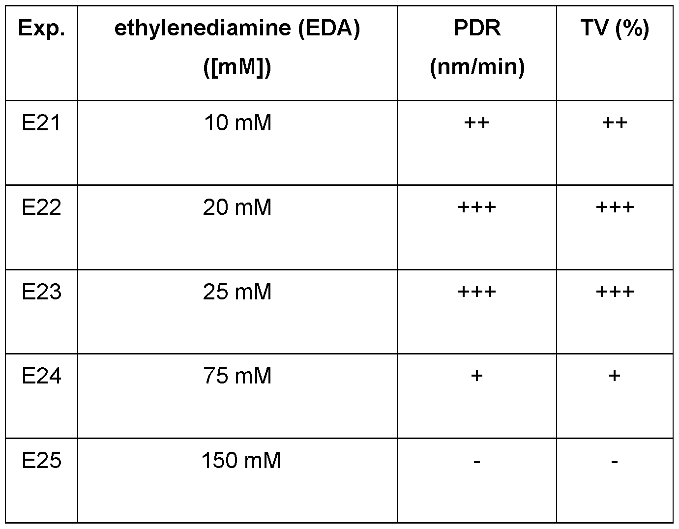
- Respective test compositions were prepared freshly comprising E1 to E25 (weight: appr. 0.27 g/L - 0.53 g/L Pd 2+ ) between 2.5 mM and 5.0 mM of palladium ions (e.g. palladium sulfate or palladium chloride as palladium source) (see Table 1 , E1 to E5), from 5 mM to 60 mM ethylenediamine disuccinate (EDDS) (see Table 2, E6 to E10), a pH in a range from 5.0 to 7.0 (see Table 3, E11 to 15), from 25 mM to 200 mM chloride or 50 mM bromine or 10 mM iodine (see Table 4, E16 to E20), from 5 mM to 75 mM of ethylenediamine (EDA) (see Table 5, E21 to E25), and 500mM sodium formate as reducing agent.
- palladium ions e.g. palladium sulfate or palladium
- a piece of SFTB1 test vehicle (size of 142 mm x 240 mm) comprising a fresh deposited nickel or nickel-phosphorus surface at both sides, and which has rinsed, is immersed into the respective test composition for 8 - 20 minutes to achieve palladium thickness of 160 nm - 400 nm respectively at a temperature of 55°C.
- the palladium deposition rate (PDR, nm/min) of the respective test composition was determined based on thickness measurements by XRF, and the thickness variability (TV) of the palladium coating deposited on the substrate of the respective test composition was determined based on the coefficient of variance (CV), which is based on statistics theory.
- the coefficient of variance is defined as the ratio of the standard deviation to the mean and expressed usually in percentage.
- Test compositions E1 to E5 comprise between 2.5 mM and 5.0 mM of palladium ions, 11.25 - 22.5 mM of ethylenediamine (EDA) with ratio 1 : 4.5 of palladium to EDA, 7.5 mM ethylenediamine disuccinate (EDDS), 50 mM chloride, and 500 mM of formate as reducing agent at pH of 5.8.
- EDA ethylenediamine
- EDDS ethylenediamine disuccinate
- 50 mM chloride 50 mM chloride
- 500 mM of formate as reducing agent at pH of 5.8.
- Test compositions E6 to E10 comprise 5 mM of palladium ions, from 5 mM to 60 mM of ethylenediamine disuccinate (EDDS), 50mM chloride, 22.5 mM of ethylenediamine (EDA), and 500 mM of formate as reducing agent at pH of 5.8.
- Test compositions E11 to E15 comprise 5.0 mM of palladium ions, 5 mM of ethylenediamine disuccinate (EDDS), a pH between 5.0 and 7.0, 50 mM chloride, 22.5 mM of ethylenediamine (EDA), and 500 mM of formate as reducing agent.
- the optimal palladium deposition rate (PDR) and thickness variability (TV) of the palladium coating can be observed in a pH range between 5.8 (E12) and 6.5 (E13), while a pH of 5.0 (E11) or less leads to a significant bath instability.
- pH value of 6.8 (E14) or 7.0 (E15) or higher results in a significant de- crease in palladium deposition rate (PDR) or even no palladium plating and also results in a significant increase of thickness variability (TV) of the palladium coating.
- Test compositions E16 to E20 comprise 5 mM of palladium ions, 5 mM of ethylenediamine disuccinate (EDDS), between 25 mM (E16) and 200 mM (E18) chloride or 50 mM bromide (E19) or 10 mM iodide (E20), 22.5 mM of ethylenediamine (EDA), and 500 mM of formate as reducing agent at pH of 5.8.
- Test compositions E21 to E25 comprise 5.0 mM of palladium ions, 5 mM of ethylenediamine disuccinate (EDDS), 50 mM chloride, between 10 mM and 150 mM of ethylenedi- amine (EDA), and 500mM of formate as reducing agent at pH of 5.8.
- EDDS ethylenediamine disuccinate
- EDA ethylenedi- amine
- the ethylenediamine (EDA) concentration over a concentration range from 10mM (E21) to 25 mM (E23) allows for an excellent palladium deposition, according to excellent palladium deposition rates and thickness variability, while eth- ylenediamine (EDA) concentration of 75 mM leads to a significant drop of palladium deposition rate and poor thickness variability, while150 mM (E25) or higher impairs the palladium deposition process.
Landscapes
- Chemical & Material Sciences (AREA)
- Engineering & Computer Science (AREA)
- Metallurgy (AREA)
- Chemical Kinetics & Catalysis (AREA)
- Materials Engineering (AREA)
- Mechanical Engineering (AREA)
- Organic Chemistry (AREA)
- General Chemical & Material Sciences (AREA)
- Manufacturing & Machinery (AREA)
- Microelectronics & Electronic Packaging (AREA)
- Inorganic Chemistry (AREA)
- Physics & Mathematics (AREA)
- Thermal Sciences (AREA)
- Chemically Coating (AREA)
Abstract
Description


Claims
Priority Applications (4)
| Application Number | Priority Date | Filing Date | Title |
|---|---|---|---|
| JP2023513809A JP7846675B2 (en) | 2020-08-31 | 2021-08-31 | Composition for depositing palladium coating on a substrate |
| US18/042,791 US20230323542A1 (en) | 2020-08-31 | 2021-08-31 | Compostion for depositing a palladium coating on a substrate |
| CN202180050663.2A CN116249797A (en) | 2020-08-31 | 2021-08-31 | Compositions for depositing palladium coatings on substrates |
| KR1020237006279A KR20230058391A (en) | 2020-08-31 | 2021-08-31 | Compositions for Depositing Palladium Coatings on Substrates |
Applications Claiming Priority (2)
| Application Number | Priority Date | Filing Date | Title |
|---|---|---|---|
| EP20193722.4 | 2020-08-31 | ||
| EP20193722.4A EP3960898A1 (en) | 2020-08-31 | 2020-08-31 | Compostion for depositing a palladium coating on a substrate |
Publications (1)
| Publication Number | Publication Date |
|---|---|
| WO2022043567A1 true WO2022043567A1 (en) | 2022-03-03 |
Family
ID=72292444
Family Applications (1)
| Application Number | Title | Priority Date | Filing Date |
|---|---|---|---|
| PCT/EP2021/073932 Ceased WO2022043567A1 (en) | 2020-08-31 | 2021-08-31 | Compostion for depositing a palladium coating on a substrate |
Country Status (6)
| Country | Link |
|---|---|
| US (1) | US20230323542A1 (en) |
| EP (1) | EP3960898A1 (en) |
| JP (1) | JP7846675B2 (en) |
| KR (1) | KR20230058391A (en) |
| CN (1) | CN116249797A (en) |
| WO (1) | WO2022043567A1 (en) |
Citations (9)
| Publication number | Priority date | Publication date | Assignee | Title |
|---|---|---|---|---|
| US3285754A (en) | 1962-07-05 | 1966-11-15 | Johnson Matthey Co Ltd | Deposition of palladium |
| US4424241A (en) | 1982-09-27 | 1984-01-03 | Bell Telephone Laboratories, Incorporated | Electroless palladium process |
| EP0698130B1 (en) | 1993-05-13 | 1997-04-23 | ATOTECH Deutschland GmbH | Process for the deposition of palladium layers |
| JPH11269658A (en) * | 1998-03-24 | 1999-10-05 | Ishihara Chem Co Ltd | Electroless palladium plating solution |
| US6336962B1 (en) * | 1997-10-08 | 2002-01-08 | Atotech Deutschland Gmbh | Method and solution for producing gold coating |
| US20090044720A1 (en) * | 2007-08-15 | 2009-02-19 | Kojima Chemicals Co., Ltd. | Electroless palladium plating solution |
| US20090081369A1 (en) * | 2005-07-20 | 2009-03-26 | Akihiro Aiba | Electroless Palladium Plating Liquid |
| US20160053379A1 (en) * | 2013-03-27 | 2016-02-25 | Atotech Deutschland Gmbh | Electroless copper plating solution |
| US20170130337A1 (en) * | 2010-07-20 | 2017-05-11 | Tdk Corporation | Coating and electronic component |
Family Cites Families (9)
| Publication number | Priority date | Publication date | Assignee | Title |
|---|---|---|---|---|
| JP3035763B2 (en) * | 1993-08-30 | 2000-04-24 | 小島化学薬品株式会社 | Electroless palladium plating solution |
| GB9422762D0 (en) * | 1994-11-11 | 1995-01-04 | Ass Octel | Use of a compound |
| JP2001342453A (en) | 2000-06-01 | 2001-12-14 | Mitsubishi Rayon Co Ltd | Chelating composition |
| KR100688833B1 (en) | 2005-10-25 | 2007-03-02 | 삼성전기주식회사 | Plating layer formation method of a printed circuit board and a printed circuit board manufactured therefrom |
| US20140072706A1 (en) | 2012-09-11 | 2014-03-13 | Ernest Long | Direct Electroless Palladium Plating on Copper |
| WO2015155173A1 (en) | 2014-04-10 | 2015-10-15 | Atotech Deutschland Gmbh | Plating bath composition and method for electroless plating of palladium |
| SG11201700463TA (en) | 2014-08-15 | 2017-02-27 | Atotech Deutschland Gmbh | Method for reducing the optical reflectivity of a copper and copper alloy circuitry and touch screen device |
| US20160145745A1 (en) | 2014-11-24 | 2016-05-26 | Rohm And Haas Electronic Materials Llc | Formaldehyde-free electroless metal plating compositions and methods |
| ES2773771T3 (en) | 2017-05-23 | 2020-07-14 | Saxonia Edelmetalle Gmbh | Preparation of noble metal salt, a method for the preparation thereof, and use for electroplating |
-
2020
- 2020-08-31 EP EP20193722.4A patent/EP3960898A1/en active Pending
-
2021
- 2021-08-31 WO PCT/EP2021/073932 patent/WO2022043567A1/en not_active Ceased
- 2021-08-31 KR KR1020237006279A patent/KR20230058391A/en active Pending
- 2021-08-31 JP JP2023513809A patent/JP7846675B2/en active Active
- 2021-08-31 US US18/042,791 patent/US20230323542A1/en active Pending
- 2021-08-31 CN CN202180050663.2A patent/CN116249797A/en active Pending
Patent Citations (10)
| Publication number | Priority date | Publication date | Assignee | Title |
|---|---|---|---|---|
| US3285754A (en) | 1962-07-05 | 1966-11-15 | Johnson Matthey Co Ltd | Deposition of palladium |
| US4424241A (en) | 1982-09-27 | 1984-01-03 | Bell Telephone Laboratories, Incorporated | Electroless palladium process |
| EP0698130B1 (en) | 1993-05-13 | 1997-04-23 | ATOTECH Deutschland GmbH | Process for the deposition of palladium layers |
| US6336962B1 (en) * | 1997-10-08 | 2002-01-08 | Atotech Deutschland Gmbh | Method and solution for producing gold coating |
| JPH11269658A (en) * | 1998-03-24 | 1999-10-05 | Ishihara Chem Co Ltd | Electroless palladium plating solution |
| US20090081369A1 (en) * | 2005-07-20 | 2009-03-26 | Akihiro Aiba | Electroless Palladium Plating Liquid |
| US7704307B2 (en) | 2005-07-20 | 2010-04-27 | Nippon Mining & Metals Co., Ltd. | Electroless palladium plating liquid |
| US20090044720A1 (en) * | 2007-08-15 | 2009-02-19 | Kojima Chemicals Co., Ltd. | Electroless palladium plating solution |
| US20170130337A1 (en) * | 2010-07-20 | 2017-05-11 | Tdk Corporation | Coating and electronic component |
| US20160053379A1 (en) * | 2013-03-27 | 2016-02-25 | Atotech Deutschland Gmbh | Electroless copper plating solution |
Also Published As
| Publication number | Publication date |
|---|---|
| CN116249797A (en) | 2023-06-09 |
| EP3960898A1 (en) | 2022-03-02 |
| KR20230058391A (en) | 2023-05-03 |
| TW202217065A (en) | 2022-05-01 |
| JP7846675B2 (en) | 2026-04-15 |
| US20230323542A1 (en) | 2023-10-12 |
| JP2023539306A (en) | 2023-09-13 |
Similar Documents
| Publication | Publication Date | Title |
|---|---|---|
| TW301844B (en) | ||
| KR101996915B1 (en) | Substitution type electroless gold plating bath containing purine or pyrimidine-based compound having carbonyl oxygen and substitution type electroless gold plating using the same | |
| US5882736A (en) | palladium layers deposition process | |
| EP1781421B1 (en) | Silver plating in electronics manufacture | |
| US9249513B2 (en) | Beta-amino acid comprising plating formulation | |
| JP2918339B2 (en) | Palladium layer deposition method | |
| EP0060294A1 (en) | PLATING OF ALLOYS WITHOUT ELECTRICAL CURRENT. | |
| TW201720955A (en) | Plating bath composition for electroless plating of gold and a method for depositing a gold layer | |
| WO2023144003A1 (en) | Composition for depositing a palladium coating on an activated copper-coated substrate | |
| KR20180037962A (en) | Compositions and methods for electroless plating of copper on palladium, and coated parts therefrom | |
| CN101634021B (en) | Electroless gold plating solution | |
| KR20130055956A (en) | Transferring method for conductive mesh | |
| WO2022043567A1 (en) | Compostion for depositing a palladium coating on a substrate | |
| EP3792374B1 (en) | Electroless copper plating bath | |
| TWI804539B (en) | Electroless gold plating bath | |
| TWI918707B (en) | Compostion for depositing a palladium coating on a substrate | |
| JP2004512429A (en) | Lead-free chemical nickel alloy | |
| US20190085461A1 (en) | Water soluble and air stable phosphaadamantanes as stabilizers for electroless metal deposition | |
| JP3227505B2 (en) | Substitution type electroless gold plating solution | |
| KR101483599B1 (en) | An electroless gold plating solution | |
| EP4407067A1 (en) | Plating bath composition for plating of precious metal and a method for depositing a precious metal layer | |
| JP5066691B2 (en) | Method to stabilize electroless gold plating bath | |
| US20170350016A1 (en) | Use of Water Soluble Lanthanide Compounds As Stabilizer In Electrolytes For Electroless Metal Deposition | |
| HK1002869B (en) | Printed circuit board manufacture |
Legal Events
| Date | Code | Title | Description |
|---|---|---|---|
| 121 | Ep: the epo has been informed by wipo that ep was designated in this application |
Ref document number: 21770183 Country of ref document: EP Kind code of ref document: A1 |
|
| ENP | Entry into the national phase |
Ref document number: 2023513809 Country of ref document: JP Kind code of ref document: A |
|
| WWE | Wipo information: entry into national phase |
Ref document number: 202327022220 Country of ref document: IN |
|
| NENP | Non-entry into the national phase |
Ref country code: DE |
|
| 122 | Ep: pct application non-entry in european phase |
Ref document number: 21770183 Country of ref document: EP Kind code of ref document: A1 |