WO2022030366A1 - 表示素子、表示装置および電子機器 - Google Patents
表示素子、表示装置および電子機器 Download PDFInfo
- Publication number
- WO2022030366A1 WO2022030366A1 PCT/JP2021/028184 JP2021028184W WO2022030366A1 WO 2022030366 A1 WO2022030366 A1 WO 2022030366A1 JP 2021028184 W JP2021028184 W JP 2021028184W WO 2022030366 A1 WO2022030366 A1 WO 2022030366A1
- Authority
- WO
- WIPO (PCT)
- Prior art keywords
- unit
- image
- substrate
- phase modulation
- light
- Prior art date
- Legal status (The legal status is an assumption and is not a legal conclusion. Google has not performed a legal analysis and makes no representation as to the accuracy of the status listed.)
- Ceased
Links
Images













Classifications
-
- H—ELECTRICITY
- H10—SEMICONDUCTOR DEVICES; ELECTRIC SOLID-STATE DEVICES NOT OTHERWISE PROVIDED FOR
- H10K—ORGANIC ELECTRIC SOLID-STATE DEVICES
- H10K59/00—Integrated devices, or assemblies of multiple devices, comprising at least one organic light-emitting element covered by group H10K50/00
- H10K59/80—Constructional details
- H10K59/8791—Arrangements for improving contrast, e.g. preventing reflection of ambient light
-
- G—PHYSICS
- G02—OPTICS
- G02F—OPTICAL DEVICES OR ARRANGEMENTS FOR THE CONTROL OF LIGHT BY MODIFICATION OF THE OPTICAL PROPERTIES OF THE MEDIA OF THE ELEMENTS INVOLVED THEREIN; NON-LINEAR OPTICS; FREQUENCY-CHANGING OF LIGHT; OPTICAL LOGIC ELEMENTS; OPTICAL ANALOGUE/DIGITAL CONVERTERS
- G02F1/00—Devices or arrangements for the control of the intensity, colour, phase, polarisation or direction of light arriving from an independent light source, e.g. switching, gating or modulating; Non-linear optics
- G02F1/01—Devices or arrangements for the control of the intensity, colour, phase, polarisation or direction of light arriving from an independent light source, e.g. switching, gating or modulating; Non-linear optics for the control of the intensity, phase, polarisation or colour
-
- G—PHYSICS
- G02—OPTICS
- G02F—OPTICAL DEVICES OR ARRANGEMENTS FOR THE CONTROL OF LIGHT BY MODIFICATION OF THE OPTICAL PROPERTIES OF THE MEDIA OF THE ELEMENTS INVOLVED THEREIN; NON-LINEAR OPTICS; FREQUENCY-CHANGING OF LIGHT; OPTICAL LOGIC ELEMENTS; OPTICAL ANALOGUE/DIGITAL CONVERTERS
- G02F1/00—Devices or arrangements for the control of the intensity, colour, phase, polarisation or direction of light arriving from an independent light source, e.g. switching, gating or modulating; Non-linear optics
- G02F1/01—Devices or arrangements for the control of the intensity, colour, phase, polarisation or direction of light arriving from an independent light source, e.g. switching, gating or modulating; Non-linear optics for the control of the intensity, phase, polarisation or colour
- G02F1/13—Devices or arrangements for the control of the intensity, colour, phase, polarisation or direction of light arriving from an independent light source, e.g. switching, gating or modulating; Non-linear optics for the control of the intensity, phase, polarisation or colour based on liquid crystals, e.g. single liquid crystal display cells
-
- G—PHYSICS
- G02—OPTICS
- G02F—OPTICAL DEVICES OR ARRANGEMENTS FOR THE CONTROL OF LIGHT BY MODIFICATION OF THE OPTICAL PROPERTIES OF THE MEDIA OF THE ELEMENTS INVOLVED THEREIN; NON-LINEAR OPTICS; FREQUENCY-CHANGING OF LIGHT; OPTICAL LOGIC ELEMENTS; OPTICAL ANALOGUE/DIGITAL CONVERTERS
- G02F1/00—Devices or arrangements for the control of the intensity, colour, phase, polarisation or direction of light arriving from an independent light source, e.g. switching, gating or modulating; Non-linear optics
- G02F1/01—Devices or arrangements for the control of the intensity, colour, phase, polarisation or direction of light arriving from an independent light source, e.g. switching, gating or modulating; Non-linear optics for the control of the intensity, phase, polarisation or colour
- G02F1/13—Devices or arrangements for the control of the intensity, colour, phase, polarisation or direction of light arriving from an independent light source, e.g. switching, gating or modulating; Non-linear optics for the control of the intensity, phase, polarisation or colour based on liquid crystals, e.g. single liquid crystal display cells
- G02F1/133—Constructional arrangements; Operation of liquid crystal cells; Circuit arrangements
- G02F1/1333—Constructional arrangements; Manufacturing methods
- G02F1/1335—Structural association of cells with optical devices, e.g. polarisers or reflectors
-
- G—PHYSICS
- G02—OPTICS
- G02F—OPTICAL DEVICES OR ARRANGEMENTS FOR THE CONTROL OF LIGHT BY MODIFICATION OF THE OPTICAL PROPERTIES OF THE MEDIA OF THE ELEMENTS INVOLVED THEREIN; NON-LINEAR OPTICS; FREQUENCY-CHANGING OF LIGHT; OPTICAL LOGIC ELEMENTS; OPTICAL ANALOGUE/DIGITAL CONVERTERS
- G02F1/00—Devices or arrangements for the control of the intensity, colour, phase, polarisation or direction of light arriving from an independent light source, e.g. switching, gating or modulating; Non-linear optics
- G02F1/01—Devices or arrangements for the control of the intensity, colour, phase, polarisation or direction of light arriving from an independent light source, e.g. switching, gating or modulating; Non-linear optics for the control of the intensity, phase, polarisation or colour
- G02F1/13—Devices or arrangements for the control of the intensity, colour, phase, polarisation or direction of light arriving from an independent light source, e.g. switching, gating or modulating; Non-linear optics for the control of the intensity, phase, polarisation or colour based on liquid crystals, e.g. single liquid crystal display cells
- G02F1/133—Constructional arrangements; Operation of liquid crystal cells; Circuit arrangements
- G02F1/1333—Constructional arrangements; Manufacturing methods
- G02F1/1335—Structural association of cells with optical devices, e.g. polarisers or reflectors
- G02F1/1336—Illuminating devices
-
- G—PHYSICS
- G02—OPTICS
- G02F—OPTICAL DEVICES OR ARRANGEMENTS FOR THE CONTROL OF LIGHT BY MODIFICATION OF THE OPTICAL PROPERTIES OF THE MEDIA OF THE ELEMENTS INVOLVED THEREIN; NON-LINEAR OPTICS; FREQUENCY-CHANGING OF LIGHT; OPTICAL LOGIC ELEMENTS; OPTICAL ANALOGUE/DIGITAL CONVERTERS
- G02F1/00—Devices or arrangements for the control of the intensity, colour, phase, polarisation or direction of light arriving from an independent light source, e.g. switching, gating or modulating; Non-linear optics
- G02F1/01—Devices or arrangements for the control of the intensity, colour, phase, polarisation or direction of light arriving from an independent light source, e.g. switching, gating or modulating; Non-linear optics for the control of the intensity, phase, polarisation or colour
- G02F1/13—Devices or arrangements for the control of the intensity, colour, phase, polarisation or direction of light arriving from an independent light source, e.g. switching, gating or modulating; Non-linear optics for the control of the intensity, phase, polarisation or colour based on liquid crystals, e.g. single liquid crystal display cells
- G02F1/133—Constructional arrangements; Operation of liquid crystal cells; Circuit arrangements
- G02F1/1333—Constructional arrangements; Manufacturing methods
- G02F1/1347—Arrangement of liquid crystal layers or cells in which the final condition of one light beam is achieved by the addition of the effects of two or more layers or cells
-
- G—PHYSICS
- G09—EDUCATION; CRYPTOGRAPHY; DISPLAY; ADVERTISING; SEALS
- G09F—DISPLAYING; ADVERTISING; SIGNS; LABELS OR NAME-PLATES; SEALS
- G09F9/00—Indicating arrangements for variable information in which the information is built-up on a support by selection or combination of individual elements
- G09F9/30—Indicating arrangements for variable information in which the information is built-up on a support by selection or combination of individual elements in which the desired character or characters are formed by combining individual elements
-
- G—PHYSICS
- G09—EDUCATION; CRYPTOGRAPHY; DISPLAY; ADVERTISING; SEALS
- G09F—DISPLAYING; ADVERTISING; SIGNS; LABELS OR NAME-PLATES; SEALS
- G09F9/00—Indicating arrangements for variable information in which the information is built-up on a support by selection or combination of individual elements
- G09F9/46—Indicating arrangements for variable information in which the information is built-up on a support by selection or combination of individual elements in which the desired character is selected from a number of characters arranged one behind the other
-
- H—ELECTRICITY
- H05—ELECTRIC TECHNIQUES NOT OTHERWISE PROVIDED FOR
- H05B—ELECTRIC HEATING; ELECTRIC LIGHT SOURCES NOT OTHERWISE PROVIDED FOR; CIRCUIT ARRANGEMENTS FOR ELECTRIC LIGHT SOURCES, IN GENERAL
- H05B33/00—Electroluminescent light sources
- H05B33/12—Light sources with substantially two-dimensional [2D] radiating surfaces
Definitions
- This disclosure relates to display elements, display devices and electronic devices. More specifically, the present invention relates to a display element capable of individually modulating the intensity and phase of light, a display device including the display element, and an electronic device including the display device.
- Patent Document 1 discloses that phase modulation is performed using a panel using a liquid crystal material.
- an object of the present disclosure is to provide a display element capable of reducing an increase in calculation cost and deterioration of image quality, a display device provided with such a display element, and an electronic device provided with such a display device. ..
- the display element according to the present disclosure for achieving the above object is An image display unit that displays an image consisting of luminance-modulated coherent light, and A phase modulation unit that performs phase modulation on the light from the image display unit, It is a display element having.
- the display device for achieving the above object is An image display unit that displays an image consisting of luminance-modulated coherent light, and A phase modulation unit that performs phase modulation on the light from the image display unit, It is a display device including a display element having the above.
- the electronic devices pertaining to this disclosure to achieve the above objectives are: An image display unit that displays an image consisting of luminance-modulated coherent light, and A phase modulation unit that performs phase modulation on the light from the image display unit, It is an electronic device using a display device including a display element having the above.
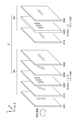
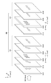
- FIG. 1 is a schematic perspective view when the display device according to the first embodiment is virtually separated.
- FIG. 2 is a block diagram of a display element used in the first embodiment.
- FIG. 3 is a schematic partial cross-sectional view of a substrate or the like for explaining the structure of the display element.
- FIG. 4 is a schematic configuration diagram showing the arrangement relationship of the optical elements constituting the display element.
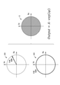
- FIG. 5 is a diagram showing that complete phase modulation can be obtained by combining luminance modulation and phase modulation.
- FIG. 6 is a schematic configuration diagram showing an arrangement of optical elements constituting the display element according to the first modification.
- FIG. 7 is a schematic partial cross-sectional view of a substrate or the like for explaining the structure of the display element according to the first modification.
- FIG. 1 is a schematic perspective view when the display device according to the first embodiment is virtually separated.
- FIG. 2 is a block diagram of a display element used in the first embodiment.
- FIG. 3 is a schematic partial cross-sectional view of
- FIG. 8 is a schematic configuration diagram showing an arrangement of optical elements constituting the display element according to the second modification.
- FIG. 9 is a schematic partial cross-sectional view of a substrate or the like for explaining the structure of the display element according to the second modification.
- FIG. 10 is a schematic partial cross-sectional view of a substrate or the like for explaining the structure of the display element according to the third modification.
- FIG. 11 is a schematic partial cross-sectional view of a substrate or the like for explaining the structure of the display element according to the fourth modification.
- FIG. 12 is a schematic partial cross-sectional view of a substrate or the like for explaining the structure of the display element according to the fifth modification.
- FIG. 13 is a schematic partial cross-sectional view of a substrate or the like for explaining the structure of the display element according to the sixth modification.
- FIG. 14 is a schematic partial cross-sectional view of a substrate or the like for explaining the structure of the display element according to the seventh modification.
- FIG. 15 is a diagram for explaining an eighth modification, and is a conceptual diagram showing a configuration of a display device that displays colors using three display elements.
- FIG. 16 is a diagram for explaining an eighth modification, following FIG. 15, and is a conceptual diagram showing a configuration of a display device that displays a color using one display element.
- FIG. 17 is a schematic partial plan view for explaining the arrangement of color filters.
- FIG. 18 is a schematic partial plan view for explaining the arrangement of color filters, following FIG. FIG.
- FIG. 19 is a schematic diagram for explaining a configuration of a display device using the display element according to the ninth modification.
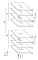
- FIG. 20 is a schematic diagram for explaining the configuration of the display device according to the second embodiment.
- FIG. 21 is a schematic configuration diagram showing the arrangement relationship of the optical elements constituting the display element.
- FIG. 22 is a schematic configuration diagram showing the arrangement relationship of the optical elements constituting the display element, following FIG. 21.
- FIG. 23 is a schematic partial cross-sectional view of a substrate or the like for explaining the structure of the display element.
- FIG. 24 is a conceptual diagram of the display device according to the third embodiment.
- FIG. 25 is a conceptual diagram for explaining a first modification of the third embodiment.
- FIG. 26 is a conceptual diagram for explaining a second modification of the third embodiment.
- FIG. 27 is a conceptual diagram for explaining a configuration example of a projection type display device.
- FIG. 28 is a conceptual diagram for explaining a configuration example of a projection type display device adopting a three-panel system.
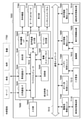
- FIG. 29 is a block diagram showing an example of a schematic configuration of a vehicle control system.
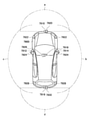
- FIG. 30 is an explanatory diagram showing an example of the installation positions of the vehicle exterior information detection unit and the image pickup unit.
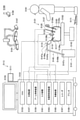
- FIG. 31 is a diagram schematically showing the overall configuration of the operating room system.
- FIG. 32 is a diagram showing a display example of an operation screen on the centralized operation panel.
- FIG. 33 is a diagram showing an example of a state of surgery to which the operating room system is applied.
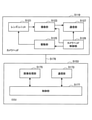
- FIG. 34 is a block diagram showing an example of the functional configuration of the camera head and the CCU shown in FIG. 33.
- the display device according to the present disclosure and the display device used for the electronic device according to the present disclosure may be simply referred to as “the display device of the present disclosure”.
- the display element according to the present disclosure and the display device used in the display device of the present disclosure may be simply referred to as "the display element of the present disclosure”.
- the display element of the present disclosure, the display device of the present disclosure, and the electronic device according to the present disclosure may be simply referred to as "the present disclosure”.
- the display element of the present disclosure is An image display unit that displays an image consisting of luminance-modulated coherent light, and A phase modulation unit that performs phase modulation on the light from the image display unit, have.
- the phase modulator It includes a first substrate having a first electrode arranged in a matrix, a second substrate having a second electrode, and a liquid crystal material layer arranged between the first substrate and the second substrate. Based on the voltage applied between the first electrode and the second electrode, the light incident from the image display unit can be phase-modulated.
- the image display unit is It includes a third substrate having pixel electrodes arranged in a matrix, a fourth substrate having a common electrode, and a liquid crystal material layer arranged between the third substrate and the fourth substrate.
- Luminance modulation can be applied to the coherent light incident on the image display unit based on the voltage applied between the pixel electrode and the common electrode.
- the display element of the present disclosure it is possible to obtain an output in which the amplitude A of light and the phase ⁇ are individually modulated.
- the ability to individually modulate the amplitude A and the phase ⁇ of light is referred to as complete phase modulation.
- the propagation of light is reproduced by controlling the spatial distribution of the phase of light, and the image is displayed by controlling the distance of image formation. The observer recognizes the image based on the light from which the light from the image display unit is further appropriately phase-modulated.
- the image display is transmissive or reflective and
- the image display unit and the phase modulation unit are stacked, It can be configured.
- the bonding method includes, for example, a bonding method using an adhesive, a bonding method in which a coated glass paste or the like is welded with a laser, or the surface is activated. It is possible to use a method of bonding by laminating afterwards by an interatomic force or a method of bonding by chemical bonding with a reaction solution applied. Qualitatively, due to the characteristics of the display element, it is preferable to make the joint portion as narrow as possible. Although it depends on the material to be bonded, it is basically preferable to bond by an interatomic force or a chemical bond.
- one of the first substrate and the second substrate of the phase modulation unit and one of the third substrate and the fourth substrate of the image display portion are laminated so as to face each other.
- the configuration may be such that either one of the first substrate and the second substrate of the phase modulation unit and one of the third substrate and the fourth substrate of the image display unit are shared. ..
- the microlenses arranged in a matrix can be arranged between the image display unit and the phase modulation unit.
- a color filter may be arranged at at least one of the image display unit and the phase modulation unit.
- the color filter may be configured to be arranged in a stripe shape for each type of transparent color.
- the color filter can be configured such that stripes of the same transparent color are arranged so as not to be adjacent to each other.
- the color filter may be configured such that a plurality of adjacent stripes are arranged so as to have the same transparent color.
- the propagation of light is reproduced by controlling the spatial distribution of the phase of light, and the image is displayed by controlling the distance of image formation. Therefore, the observer recognizes an image in which the image displayed by the image display unit is further appropriately phase-modulated. Therefore, even if the display area of the display element is roughly classified for each predetermined color, the image can be displayed without any trouble by controlling the phase modulation unit.
- the image display unit instead of the above-mentioned image display unit including the liquid crystal material layer, The image display unit has a light emitting element that emits coherent light arranged in a matrix. By controlling the brightness of the light emitting element, an image composed of coherent light can be displayed.
- the image display unit and the phase modulation unit can be configured to be laminated.
- the configuration of the light emitting element is not particularly limited as long as the implementation of the present disclosure is not hindered.
- the light emitting element include a semiconductor laser element, an LED element, and an organic electroluminescence element.
- a light emitting element that emits coherent light can be configured. From the viewpoint of constituting a flat display element, it is preferable that the light emitting element is composed of an organic electroluminescence element.
- a splitter may be arranged between the image display unit and the phase modulation unit.
- a splitter may be arranged on the emission side of the phase modulation unit.
- the display device of the present disclosure is An image display unit that displays an image consisting of luminance-modulated coherent light, and A phase modulation unit that performs phase modulation on the light from the image display unit, Includes display elements that have.
- the display device can be configured to have a light source unit that irradiates the image display unit with coherent light.
- a light source unit that irradiates coherent light for example, a light source using a semiconductor laser element can be mentioned.
- a film made of polyimide can be used as a substrate.
- a suitable material may be appropriately selected and used in consideration of the translucency required for the display element and the like.
- the phase modulation unit has a first substrate having a first electrode arranged in a matrix, a second substrate having a second electrode, and a liquid crystal material layer arranged between the first substrate and the second substrate.
- the first electrode and the second electrode can be formed by using a transparent conductive material such as indium tin oxide (ITO) or indium zinc oxide (IZO).
- ITO indium tin oxide
- IZO indium zinc oxide
- a metal film thin enough to have light transmission can be used.
- the image display unit includes a third substrate having pixel electrodes arranged in a matrix, a fourth substrate having common electrodes, and a liquid crystal material layer arranged between the third substrate and the fourth substrate.
- the common electrode can be formed by using a transparent conductive material such as indium tin oxide (ITO) or indium zinc oxide (IZO). In some cases, a metal film thin enough to have light transmission can be used.
- the image display unit is a transmissive type
- the pixel electrode can be formed by using the same material as the common electrode.
- the pixel electrode can be formed by using a metal material such as silver (Ag) or aluminum (Al).
- an alignment film for defining the initial orientation of the liquid crystal molecules is provided on the surface in contact with the liquid crystal material layer.
- the alignment film can be formed by using a well-known material such as an organic compound or an inorganic compound.
- an alignment film made of an inorganic material having excellent light resistance.
- the alignment film made of an inorganic material can be formed, for example, by depositing an inorganic material such as silicon oxide from an oblique direction with respect to the substrate.
- the configuration of the polarizing element used in the display element is not particularly limited, and for example, an absorption type polarizing element formed of a stretched resin or the like or a reflective type polarizing element such as a wire grid polarizing element is used. Can be done.
- the wire grid polarizing element has an advantage that it has excellent heat resistance and can be arranged in an in-cell in a phase modulation unit or an image display unit.
- the first electrode arranged in a matrix and the pixel electrodes arranged in a matrix can be driven by using, for example, a transistor constituting a switching element.
- a transistor constituting a switching element As the transistor, in addition to the so-called thin film transistor, a transistor provided in the well region of the semiconductor substrate can be used.
- the materials constituting the various wirings and contacts used in the present disclosure are not particularly limited, and are, for example, aluminum (Al), aluminum alloys such as Al—Cu and Al—Si, tungsten (W), and tungsten silicide (WSi). Metallic materials such as tungsten alloys such as x ) can be used.
- the insulating layer and the material constituting the insulating film used in the present disclosure are not particularly limited as long as they do not interfere with the implementation of the present disclosure.
- an inorganic material such as silicon oxide or an organic material such as polyimide can be used.
- the display device may be configured to display a monochrome image or may be configured to display a color image.
- pixel values of the liquid crystal display device U-XGA (1600,1200), HD-TV (1920,1080), Q-XGA (2048,1536), (3840,2160), (7680,)
- Some of the image resolutions, such as 4320) can be exemplified, but are not limited to these values.
- a direct-view type or a projection type display device can be exemplified.
- various electronic devices having an image display function can be exemplified.
- the first embodiment relates to a display element, a display device, and an electronic device according to the present disclosure.
- FIG. 1 is a schematic perspective view when the display device according to the first embodiment is virtually separated.
- the display device 1 includes a light source unit 2 that irradiates coherent light and a display element 3.
- the light source unit 2 is, for example, a light source using a vertical resonator type surface emitting laser, and irradiates the display element 3 with coherent light.
- the display element 3 has an image display unit 30 that displays an image composed of brightness-modulated coherent light, and a phase modulation unit 40 that performs phase modulation on the light from the image display unit 30. ..
- the display element 3 has a panel shape having a diagonal dimension of, for example, about 1 inch.
- the display device 1 operates based on a signal from an image control circuit (not shown), controls the distance of image formation, and displays a 2D or 3D image.
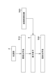
- FIG. 2 is a configuration diagram of a display element used in the first embodiment.
- the phase modulation unit 40 used in the display element 3 is configured as a so-called transmissive active matrix type liquid crystal panel.
- the phase modulation unit 40 includes various circuits such as pixels PX arranged in a matrix, a horizontal drive circuit 41 for driving the pixels PX, and a vertical drive circuit 42.
- the reference numeral SCL is a scanning line for scanning the pixel PX
- the reference numeral DTL is a signal line for supplying a seed voltage to the pixel PX.
- M pixels in the horizontal direction and N pixels in the vertical direction, for a total of M ⁇ N are arranged in a matrix.
- the image display unit 30 is also configured as a so-called transmissive active matrix type liquid crystal panel.
- the image display unit 30 is a transmissive type and is driven by a horizontal drive circuit 31 or a vertical drive circuit (not shown).
- the thickness of the liquid crystal material layer is different, and the image display unit 30 basically has the same configuration as the phase modulation unit 40.
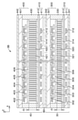
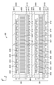
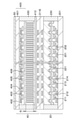
- FIG. 3 is a schematic partial cross-sectional view of a substrate or the like for explaining the structure of the display element.
- the display element 3 is configured by stacking an image display unit 30 and a phase modulation unit 40.
- one of the first substrate and the second substrate of the phase modulation unit and one of the third substrate and the fourth substrate of the image display unit face each other. It can be configured to be laminated.
- the second substrate 410 of the phase modulation unit 40 and the third substrate 300 of the image display unit 30 are laminated so as to face each other.
- Reference numeral BD indicates a junction portion between the image display unit 30 and the phase modulation unit 40.
- the image display unit 30 is arranged between the third substrate 300 having the pixel electrodes 304 arranged in a matrix, the fourth substrate 310 having the common electrode 313, and the third substrate 300 and the fourth substrate 310. It includes a liquid crystal material layer 320. Then, the coherent light incident on the image display unit 30 from the light source unit 2 is subjected to luminance modulation based on the voltage applied between the pixel electrode 304 and the common electrode 313.
- the phase modulation unit 40 is arranged between the first substrate 400 having the first electrode 404 arranged in a matrix, the second substrate 410 having the second electrode 413, and the first substrate 400 and the second substrate 410. Includes the liquid crystal material layer 420 and the like. Phase modulation is applied to the light incident from the image display unit 30 based on the voltage applied between the first electrode 404 and the second electrode 413.
- the first substrate 400 includes, for example, a substrate 401 made of quartz. On the surface of the substrate 401 on the liquid crystal material layer 420 side, the entire surface including the semiconductor material layer 402 constituting the transistor, the light-shielding portion 403 composed of wiring and electrodes, the first electrode 404, the first electrode 404, and the light-shielding portion 403.
- the provided flattening film 405 is arranged. Further, the alignment film 406 is provided on the flattening film 405.
- the second substrate 410 includes, for example, a substrate 411 made of quartz.
- the substrate 411 is formed by stacking a plurality of substrates so as to sandwich the light-shielding portion 412 corresponding to the light-shielding portion 403, for example.
- the light-shielding portion 412 may be omitted.
- a common second electrode 413 is arranged on the surface of the substrate 411 on the liquid crystal material layer 420 side. Further, an alignment film 414 is provided on the second electrode 413.
- the first substrate 400 and the second substrate 410 are sealed with the liquid crystal material layer 420 sandwiched between them.
- Reference numeral 430 indicates a sealing portion.
- the alignment films 406 and 414 set the initial orientation direction of the liquid crystal molecules 421 of the liquid crystal material layer 420. In a state where no electric field is applied to the liquid crystal material layer 420, the liquid crystal molecules 421 form a predetermined tilt angle and are oriented in a substantially vertical direction.
- the phase modulation unit 40 is a so-called vertically oriented type (VA mode) liquid crystal display.
- the third substrate 300 includes a substrate 301 made of, for example, quartz.
- the surface of the substrate 301 on the liquid crystal material layer 320 side is provided on the entire surface including the semiconductor material layer 302 constituting the transistor, the light-shielding portion 303 composed of wiring and electrodes, the pixel electrode 304, and the pixel electrode 304 and the light-shielding portion 303.
- the flattening film 305 is arranged. Further, the alignment film 306 is provided on the flattening film 305.
- the fourth substrate 310 contains, for example, a substrate 311 made of quartz.
- the substrate 311 is formed by stacking a plurality of substrates so as to sandwich the light-shielding portion 312 corresponding to the light-shielding portion 303, for example.
- the light-shielding portion 303 may be omitted.
- a common electrode 313 is arranged on the surface of the substrate 311 on the liquid crystal material layer 320 side. Further, an alignment film 314 is provided on the common electrode 313.
- the third substrate 300 and the fourth substrate 310 are sealed with the liquid crystal material layer 320 sandwiched between them.
- Reference numeral 330 indicates a sealing portion.
- the alignment films 306 and 314 set the initial orientation direction of the liquid crystal molecules 321 of the liquid crystal material layer 320. In a state where no electric field is applied to the liquid crystal material layer 320, the liquid crystal molecules 321 form a predetermined tilt angle and are oriented in a substantially vertical direction.
- the image display unit 30 is a so-called vertically oriented type (VA mode) liquid crystal device.
- a pair of polarizing elements 341 and 342 arranged so as to be in the state of cross Nicol are arranged.
- the polarizing element 341 is arranged on the fourth substrate 310 side, and the polarizing element 342 is arranged on the third substrate 300 side.
- FIG. 3 shows the arrangement in the case where the polarizing elements 341 and 342 are so-called film-shaped polarizing elements independent of the substrate, but this is only an example.
- the polarizing elements 341 and 342 may be composed of wire grid polarizing elements and may be arranged in cells on the third substrate 300 or the fourth substrate 310.
- phase modulation can be obtained by combining luminance modulation and phase modulation.
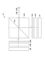
- FIG. 4 is a schematic configuration diagram showing the arrangement relationship of the optical elements constituting the display element.
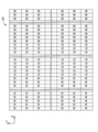
- FIG. 5 is a diagram showing that complete phase modulation can be obtained by combining luminance modulation and phase modulation.
- the coherent light from the light source unit 2 is incident on the polarizing element 341 of the image display unit 30, and linearly polarized light in a predetermined direction is incident on the liquid crystal material layer 320.
- the voltage between the pixel electrode 304 and the common electrode 313 changes the retardation of the liquid crystal material 320 sandwiched between the pixel electrode 304 and the common electrode 313.
- the linearly polarized light passes through the liquid crystal material layer 320 as it is and reaches the polarizing element 342. Since the polarizing elements 341 and 342 are in the cross-nicoled state, the light transmitted through the liquid crystal material layer 320 is blocked by the polarizing element 342 and is displayed in black.
- the polarization direction of the light transmitted through the liquid crystal material layer 320 changes by about 90 degrees and reaches the splitter 342. Therefore, the light transmitted through the liquid crystal material layer 320 is transmitted through the polarizing element 342, so that the display is white.
- the intensity of the light transmitted through the polarizing element 342 is controlled by the voltage applied to the pixel electrode 304. That is, the degree of luminance modulation is controlled by the voltage applied to the pixel electrode 304.
- Interfering light transmitted through the image display unit 30 is incident on the liquid crystal material layer 420 of the phase modulation unit 40.
- the voltage between the first electrode 404 and the second electrode 413 changes the retardation of the liquid crystal material layer 420 sandwiched between the first electrode 404 and the second electrode 413. That is, the phase of the light transmitted through the liquid crystal material layer 420 changes in the range of 0 to 2 ⁇ depending on the voltage applied to the first electrode 404. In other words, the degree of phase modulation is controlled by the voltage applied to the first electrode 404.
- the arrows attached to the alignment films 314 and 306 indicate the orientation direction of the liquid crystal molecules 321 located on the alignment film.
- the arrows attached to the alignment films 414 and 406 indicate the orientation direction of the liquid crystal molecules 421 located on the alignment film.
- the intensity of light having a predetermined phase relationship is controlled.
- the phase modulation unit 40 the phase is controlled in the range of 0 to 2 ⁇ . Therefore, by using the display element 3 in which the image display unit 30 and the phase modulation unit 40 are combined, it is possible to obtain an output in which the amplitude A of the light and the phase ⁇ are individually modulated.
- phase modulation can be obtained by combining luminance modulation and phase modulation.
- the propagation of light is reproduced by controlling the spatial distribution of the phase of light, and the image is displayed by controlling the distance of image formation.
- the observer recognizes the image based on the light from which the light from the image display unit is further appropriately phase-modulated.
- the pixels of the phase modulation unit 40 of the pixels of the image display unit 30 are basically in a one-to-one pair, and the shape of the opening is basically the same. However, it is conceivable that stray light may occur due to misalignment between the image display unit 30 and the phase modulation unit 40, diffraction of light emitted from the opening of the image display unit 30, and the like.
- the image display unit 30 and the phase modulation unit 40 are laminated as close as possible.
- the display element 3 and the display device 1 using the display element 3 can be variously modified. Hereinafter, a modified example will be described.
- FIG. 6 is a schematic configuration diagram showing an arrangement of optical elements constituting the display element according to the first modification.
- FIG. 7 is a schematic partial cross-sectional view of a substrate or the like for explaining the structure of the display element according to the first modification.
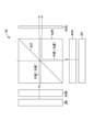
- the display element 3A shown in FIG. 6 has a configuration in which the polarizing element 342 of the image display unit 30 is omitted, and as an alternative, the polarizing element 442 is arranged on the emission side of the phase modulation unit 40.
- the polarizing element 341 on the image display unit 30 side and the polarizing element 442 on the phase modulation unit 40 side are arranged in a cross Nicol state.
- the polarizing element 442 when it is a so-called film-shaped polarizing element independent of the substrate is shown, but this is only an example.
- the polarizing element 442 may be composed of a wire grid polarizing element and may be arranged in an in-cell on the first substrate 400. The same applies to other modifications described later.
- FIG. 8 is a schematic configuration diagram showing an arrangement of optical elements constituting the display element according to the second modification.
- FIG. 9 is a schematic partial cross-sectional view of a substrate or the like for explaining the structure of the display element according to the second modification.
- the display element 3B shown in FIG. 8 has a configuration in which a polarizing element 442 is further arranged on the emission side of the phase modulation unit 40 with respect to the display element 3.
- the splitters 341 and 342 on the image display unit 30 side are arranged in a cross Nicol state.
- the polarizing element 442 on the emitting side of the phase modulation unit 40 is arranged in a state of parallel Nicol with the polarizing element 342 on the image display unit 30 side.
- This configuration has an advantage that when light other than the desired polarization direction is generated when passing through the phase modulation unit 40, it can be removed as noise.
- FIG. 10 is a schematic partial cross-sectional view of a substrate or the like for explaining the structure of the display element according to the third modification.
- the second substrate 410 of the phase modulation unit 40 and the third substrate 300 of the image display unit 30 were laminated so as to face each other.
- the first substrate 400C of the phase modulation unit 40 and the third substrate 300 of the image display unit 30 are laminated so as to face each other. Has been done.
- the positional relationship between the shading section 403 and the semiconductor material layer 402 is interchanged.
- FIG. 11 is a schematic partial cross-sectional view of a substrate or the like for explaining the structure of the display element according to the fourth modification.
- the microlens ML arranged in a matrix is arranged between the image display unit 30 and the phase modulation unit 40.
- the traveling direction of the light wrapping around the back of the light shielding unit 303 is the original traveling direction. Can be directed to.
- FIG. 12 is a schematic partial cross-sectional view of a substrate or the like for explaining the structure of the display element according to the fifth modification.
- a light-shielding wall extending in the Z direction is further provided in the light-shielding portion of the phase modulation unit.
- the light on the exit side of the image display unit 30 is one of the light due to diffraction when it passes through the opening between the light-shielding portion 303 and the light-shielding portion 303 of the third substrate 300.
- the portion wraps around behind the light-shielding portion 303.
- a light-shielding wall extending in the Z direction is further provided on the light-shielding unit 412 of the phase modulation unit 40. This makes it possible to prevent stray light due to diffraction from entering the phase modulation unit 40.
- FIG. 13 is a schematic partial cross-sectional view of a substrate or the like for explaining the structure of the display element according to the sixth modification.
- either one of the first substrate and the second substrate of the phase modulation unit, and the third substrate and the fourth substrate of the image display unit are shared with either one.
- the second substrate of the phase modulation unit 40 and the first substrate of the image display unit are shared. More specifically, the substrate 411 and the substrate 301 shown in the image display unit 3 shown in FIG. 3 are shared by the substrate 301F. According to this configuration, the joint BD shown in FIG. 3 can be omitted, and the thickness of the substrate can be reduced as a whole, so that the image display unit 30 and the phase modulation unit 40 are laminated closer to each other. be able to.
- FIG. 14 is a schematic partial cross-sectional view of a substrate or the like for explaining the structure of the display element according to the seventh modification.
- the substrate is shared between the phase modulation unit and the image display unit.
- the second substrate of the phase modulation unit 40 and the second substrate of the image display unit are shared by the substrate 311G.
- the positional relationship between the light-shielding portion 403 and the semiconductor material layer 402 is interchanged in the first substrate 400 of the phase modulation section 40.
- the eighth modification relates to a display element and a display device for performing color display.
- FIG. 15 is a diagram for explaining an eighth modification, and is a conceptual diagram showing a configuration of a display device that displays colors using three display elements.
- the display device 1A has a so-called three-plate type configuration. That is, a light source unit 2 R that emits red light, a light source unit 2 G that emits green light, and a light source unit 2 B that emits blue light are individually prepared, and are displayed independently corresponding to each light source unit. Elements 3 R , 3 G , and 3 B are arranged, and color display is performed by additive color mixing of each color.
- FIG. 16 is a diagram for explaining an eighth modification, following FIG. 15, and is a conceptual diagram showing a configuration of a display device that displays a color using one display element.
- the display device 1B has a so-called single plate type configuration.
- the light source unit 2 RGB emits light including red light, green light, and blue light.
- the display element 3H has a configuration in which a color filter is further added to the display element 3.
- the position of the color filter CF is not particularly limited.
- a color filter may be arranged on at least one of the image display unit and the phase modulation unit. Further, a plurality of color filter CFs may be arranged. In the example shown in FIG. 16, the color filter CF is arranged between the image display unit 30 and the phase modulation unit 40.
- FIG. 17 is a schematic partial plan view for explaining the arrangement of color filters.
- the color filter CF shown in FIG. 17 shows an example in which the color filters CF are arranged in a stripe shape for each type of transparent color.
- Reference numeral R, reference numeral G, and reference numeral B indicate regions of a red filter, a green filter, and a blue filter, respectively.
- the color filter CF is arranged so that stripes of the same transparent color are not adjacent to each other.
- FIG. 18 is a schematic partial plan view for explaining the arrangement of color filters, following FIG. 17.
- the color filter CF shown in FIG. 18 is also arranged in a stripe shape for each type of transparent color. However, unlike FIG. 17, the color filter CF is arranged so that a plurality of adjacent stripes have the same transparent color. More specifically, the color filter CF is divided into three areas: a region in which the red filter is continuously arranged, a region in which the green filter is continuously arranged, and a region in which the blue filter is continuously arranged.
- the propagation of light is reproduced by controlling the spatial distribution of the phase of light, and the image is displayed by controlling the distance of image formation. Therefore, the observer recognizes an image in which the image displayed by the image display unit is further appropriately phase-modulated. Therefore, even if the display area of the display element is roughly classified for each predetermined color, the image can be displayed without any trouble by controlling the phase modulation unit.
- the color filter CF shown in FIG. 17 stripes of the same transparent color are arranged so as not to be adjacent to each other. Therefore, it is difficult to narrow the pitch of the pixels as compared with the color filter CF shown in FIG. Qualitatively, the narrower the pitch of the pixels, the wider the diffraction angle and the wider the viewing range. Therefore, from the viewpoint of expanding the field of view, it is preferable to use the color filter CF shown in FIG.
- the image display unit 30 is configured as a so-called transmissive active matrix type liquid crystal panel.
- the image display unit 30 may have a reflective structure.
- FIG. 19 is a schematic diagram for explaining the configuration of a display device using the display element according to the ninth modification.
- the display device 1C has a configuration in which a light source unit 2 and a display element 3J are combined with a polarization beam splitter PBS.
- the display device 3J has a configuration in which an image display unit 30J composed of a reflection type active matrix type liquid crystal panel and a phase modulation unit 40J are combined.
- the light source unit 2 is arranged on the bottom surface of the polarizing beam splitter PBS, and the P wave light reflected at the interface of the polarizing beam splitter PBS is incident on the phase modulation unit 40J. Then, the light reflected by the reflection type image display unit 30J is transmitted through the phase modulation unit 40J, and the S wave light is transmitted through the polarization beam splitter PBS.
- the thickness of the liquid crystal material layer may be adjusted as appropriate. Generally, if the same liquid crystal material is used, the thickness of the reflective liquid crystal material layer (so-called cell gap) is about half that of the transmissive type.
- the second embodiment also relates to a display element, a display device, and an electronic device according to the present disclosure.
- FIG. 20 is a schematic diagram for explaining the configuration of the display device according to the second embodiment.
- the image display unit constituting the display element is composed of a liquid crystal panel that is not self-luminous.
- the image display unit 20 has a light emitting element that is arranged in a matrix and emits coherent light. .. Then, the image display unit 20 displays an image composed of coherent light by controlling the brightness of the light emitting element.
- a polarizing element is arranged between the image display unit 20 and the phase modulation unit 40. The coherent light from the image display unit 20 is configured to be incident on the phase modulation unit 40 via the polarizing element 50.
- FIG. 21 is a schematic configuration diagram showing the arrangement relationship of optical elements constituting the display device.
- the image display unit 20 has an organic electroluminescence element as a light emitting element.
- the light of the light emitting element is emitted as coherent light through a resonator structure or the like.
- the light from the image display unit 20 is incident on the polarizing element 50, and the linear polarization in a predetermined direction is incident on the phase modulation unit 40.
- Interfering light transmitted through the image display unit 30 is incident on the liquid crystal material layer 420 of the phase modulation unit 40.
- the voltage between the first electrode 404 and the second electrode 413 changes the retardation of the liquid crystal material layer 420 sandwiched between the first electrode 404 and the second electrode 413. That is, the phase of the light transmitted through the liquid crystal material layer 420 changes in the range of 0 to 2 ⁇ depending on the voltage applied to the first electrode 404. In other words, the degree of phase modulation is controlled by the voltage applied to the first electrode 404.
- the intensity of the light transmitted through the polarizing element 50 is controlled by the image display unit 20. Then, in the phase modulation unit 40, the phase is controlled in the range of 0 to 2 ⁇ . Therefore, the display element 3 in which the image display unit 20 and the phase modulation unit 40 are combined can obtain an output in which the amplitude A of the light and the phase ⁇ are individually modulated. As long as the implementation is not hindered, various configurations may be adopted for the arrangement position of the polarizing element 50. For example, as shown in FIG. 22, the modulator may be arranged on the display surface side of the phase modulation unit 40.
- FIG. 23 is a schematic partial cross-sectional view of a substrate or the like for explaining the structure of the display element.
- the substrate 201 is made of, for example, quartz, and the surface of the substrate 201 is provided with a wiring 201, a semiconductor material layer 202 constituting the transistor, and a pixel electrode 211 connected to one end of the transistor.
- Reference numeral 212 is a partition wall portion for partitioning between the pixel electrodes.
- An organic layer 213 including a light emitting layer is formed on the entire surface including the partition wall portion 212 and the pixel electrode 211, and the common electrode 214 is formed on the organic layer 213.
- the organic layer 213 in the portion sandwiched between the pixel electrode 211 and the common electrode 214 emits light according to the voltage between the pixel electrode 211 and the common electrode 214.
- a protective layer 221 is formed on the common electrode 214.
- the configuration on the protective layer 221 is substantially the same as the configuration of the display device 3G described with reference to FIG. In this way, the image display unit 20 and the phase modulation unit 40 are laminated.
- Reference numeral 230 is a sealing portion.
- a third embodiment also relates to a display device and an electronic device according to the present disclosure.
- the image display unit controls the light intensity
- the phase modulation unit controls the phase to perform complete phase modulation
- the output obtained by individually modulating the amplitude A and the phase ⁇ of light can be expressed as A ⁇ exp (i ⁇ ) in a mathematical formula, and this formula can be expressed as exp (i ⁇ ) by appropriately selecting the variables ⁇ 1 and ⁇ 2. 1 ) + exp (i ⁇ 2 ) can also be expressed.
- the display device of the third embodiment has a configuration in which two outputs of the phase modulation unit are appropriately superimposed.
- FIG. 24 is a conceptual diagram of the display device according to the third embodiment.
- the display device 1E has a configuration in which a pair of a light source unit that irradiates coherent light and a transmission type phase modulation unit are arranged on both of the pair of incident surfaces of the cube-type half mirror MR. That is, a light source unit 2A and a phase modulation unit 40A are arranged on the bottom surface of the half mirror MR. Further, a light source unit 2B and a phase modulation unit 40B are arranged on the left side surface of the bottom surface of the half mirror MR. Light source unit A polarizing element 50A is arranged between the light source unit 2A and the phase modulation unit 40A, and a polarizing element 50B is arranged between the light source unit 2B and the phase modulation unit 40B.
- the light transmitted through the phase modulation units 40A and 40B is set to be P wave light or S wave light.
- the light from the phase modulation unit 40B passes through the reflection surface RP of the half mirror MR as it is.
- the light from the phase modulation unit 40A is reflected by the reflection surface RP and is superimposed on the light from the phase modulation unit 40B.
- the display device 1E can also be modified in various ways. Hereinafter, a modified example will be described.
- FIG. 25 is a conceptual diagram for explaining a first modification of the third embodiment.
- the positions of the polarizing elements 50A and 50B are changed.
- the splitter 50A is arranged between the phase modulation unit 40A and the half mirror MR. Further, the splitter 50B is arranged between the phase modulation unit 40B and the half mirror MR.
- FIG. 26 is a conceptual diagram for explaining a second modification of the third embodiment.
- the splitter 50C is arranged on the exit surface of the half mirror MR.
- the light from the phase modulation unit 40A and the light from the phase modulation unit 40B are configured to be incident on the half mirror MR without passing through the polarizing element.
- the first embodiment to the third embodiment has been described above. According to the present disclosure, it is possible to obtain an output in which the amplitude A of light and the phase ⁇ are individually modulated. When displaying an image only by phase modulation, optimization and approximation by iterative calculation are required. However, in a display device using the display element of the present disclosure, complete phase modulation is possible, so that the calculation cost is high. It is possible to reduce the increase and the deterioration of the image quality.
- the display element of the present disclosure described above can be used as an element capable of individually modulating the amplitude A and the phase ⁇ of light.
- the display device of the present disclosure is used as a display unit (display device) of an electronic device in all fields for displaying a video signal input to the electronic device or a video signal generated in the electronic device as an image or a video. be able to.
- it can be used as a display unit such as a projection type display device or a head-mounted display (head-mounted display).
- the display element of the present disclosure also includes a modular one having a sealed configuration.
- the module may be provided with a circuit unit for inputting / outputting signals from the outside, a flexible printed circuit (FPC), and the like.
- FPC flexible printed circuit
- a projection type display device will be illustrated as a specific example of the electronic device using the display device of the present disclosure.
- the specific examples exemplified here are only examples, and are not limited to these.
- FIG. 27 is a conceptual diagram of a projection type display device using the display element of the present disclosure.
- the projection type display device includes a light source unit 2, an illumination optical system 510, a display element 3, an image control circuit 520 for driving the display element 3, a projection optical system 530, and the like.
- the light source unit 2 can be composed of, for example, a semiconductor light emitting element such as a semiconductor laser.
- the illumination optical system 510 is used to guide the light from the light source unit 2 to the display element 3, and a prism, a dichroic mirror, or the like is appropriately selected as needed.
- the display element 3 reproduces the propagation of light by controlling the spatial distribution of the phase of light, and controls the distance of image formation to display an image.
- FIG. 28 is a conceptual diagram for explaining a configuration example of a projection type display device adopting a three-panel system.
- the display device shown in the figure includes a display element 3 R for displaying red, a display element 3 G for displaying green, and a display element 3 B for displaying blue. These are arranged on the three entrance planes of the cross prism 515. A lens as a projection optical system 530 is arranged on the exit surface of the cross prism 515. A color filter is not required in the display element.
- a display element having the configuration described with reference to FIGS. 4, 6 to 14 can be used.
- the display device includes a light source unit 2 equipped with laser light sources of three colors of red light, green light, and blue light. As shown in the figure, the light from the light source unit 2 is separated into each color by the condenser lens 511, the dichroic mirrors 512A, 512B, the relay lens 513, and the mirrors 514A, 514B, 514C constituting the illumination optical system 510.
- the blue light separated by the dichroic mirror 512A is reflected by the mirror 514A and incident on the display element 3 B for displaying blue.
- the red light and green light transmitted through the dichroic mirror 512A are separated by the dichroic mirror 512B, and the reflected green light is incident on the display element 3G for green display.
- the red light transmitted through the dichroic mirror 512B is incident on the display element 3 R for displaying red through the relay lenses 513, mirrors 514B, and 514C.
- the light transmitted through the display elements 3R, 3G, and 3B is superimposed by the cross prism 515 and emitted to the outside via the projection optical system 530.
- the technology according to the present disclosure can be applied to various products.
- the technology according to the present disclosure is any kind of movement such as an automobile, an electric vehicle, a hybrid electric vehicle, a motorcycle, a bicycle, a personal mobility, an airplane, a drone, a ship, a robot, a construction machine, and an agricultural machine (tractor). It may be realized as a device mounted on the body.
- FIG. 29 is a block diagram showing a schematic configuration example of a vehicle control system 7000, which is an example of a mobile control system to which the technique according to the present disclosure can be applied.
- the vehicle control system 7000 includes a plurality of electronic control units connected via a communication network 7010.
- the vehicle control system 7000 includes a drive system control unit 7100, a body system control unit 7200, a battery control unit 7300, an outside information detection unit 7400, an in-vehicle information detection unit 7500, and an integrated control unit 7600. ..
- the communication network 7010 connecting these multiple control units conforms to any standard such as CAN (Controller Area Network), LIN (Local Interconnect Network), LAN (Local Area Network) or FlexRay (registered trademark). It may be an in-vehicle communication network.
- CAN Controller Area Network
- LIN Local Interconnect Network
- LAN Local Area Network
- FlexRay registered trademark
- Each control unit includes a microcomputer that performs arithmetic processing according to various programs, a storage unit that stores programs executed by the microcomputer or parameters used for various arithmetic, and a drive circuit that drives various controlled devices. To prepare for.
- Each control unit is provided with a network I / F for communicating with other control units via the communication network 7010, and is connected to devices or sensors inside and outside the vehicle by wired communication or wireless communication.
- a communication I / F for performing communication is provided. In FIG.
- the functional configuration of the integrated control unit 7600 includes a microcomputer 7610, a general-purpose communication I / F7620, a dedicated communication I / F7630, a positioning unit 7640, a beacon receiving unit 7650, an in-vehicle device I / F7660, and an audio image output unit 7670.
- the vehicle-mounted network I / F 7680 and the storage unit 7690 are illustrated.
- Other control units also include a microcomputer, a communication I / F, a storage unit, and the like.
- the drive system control unit 7100 controls the operation of the device related to the drive system of the vehicle according to various programs.
- the drive system control unit 7100 has a driving force generator for generating the driving force of the vehicle such as an internal combustion engine or a driving motor, a driving force transmission mechanism for transmitting the driving force to the wheels, and a steering angle of the vehicle. It functions as a control device such as a steering mechanism for adjusting and a braking device for generating braking force of the vehicle.
- the drive system control unit 7100 may have a function as a control device such as ABS (Antilock Brake System) or ESC (Electronic Stability Control).
- the vehicle state detection unit 7110 is connected to the drive system control unit 7100.
- the vehicle state detection unit 7110 may include, for example, a gyro sensor that detects the angular velocity of the axial rotation motion of the vehicle body, an acceleration sensor that detects the acceleration of the vehicle, an accelerator pedal operation amount, a brake pedal operation amount, or steering wheel steering. It includes at least one of sensors for detecting an angle, engine speed, wheel speed, and the like.
- the drive system control unit 7100 performs arithmetic processing using a signal input from the vehicle state detection unit 7110, and controls an internal combustion engine, a drive motor, an electric power steering device, a brake device, and the like.
- the body system control unit 7200 controls the operation of various devices mounted on the vehicle body according to various programs.
- the body system control unit 7200 functions as a keyless entry system, a smart key system, a power window device, or a control device for various lamps such as headlamps, back lamps, brake lamps, turn signals or fog lamps.
- a radio wave transmitted from a portable device that substitutes for a key or signals of various switches may be input to the body system control unit 7200.
- the body system control unit 7200 receives inputs of these radio waves or signals and controls a vehicle door lock device, a power window device, a lamp, and the like.
- the battery control unit 7300 controls the secondary battery 7310, which is the power supply source of the drive motor, according to various programs. For example, information such as the battery temperature, the battery output voltage, or the remaining capacity of the battery is input to the battery control unit 7300 from the battery device including the secondary battery 7310. The battery control unit 7300 performs arithmetic processing using these signals, and controls the temperature control of the secondary battery 7310 or the cooling device provided in the battery device.
- the vehicle outside information detection unit 7400 detects information outside the vehicle equipped with the vehicle control system 7000.
- the image pickup unit 7410 and the vehicle exterior information detection unit 7420 is connected to the vehicle exterior information detection unit 7400.
- the image pickup unit 7410 includes at least one of a ToF (Time Of Flight) camera, a stereo camera, a monocular camera, an infrared camera, and other cameras.
- the vehicle outside information detection unit 7420 is used, for example, to detect the current weather or an environment sensor for detecting the weather, or other vehicles, obstacles, pedestrians, etc. around the vehicle equipped with the vehicle control system 7000. At least one of the surrounding information detection sensors is included.
- the environment sensor may be, for example, at least one of a raindrop sensor that detects rainy weather, a fog sensor that detects fog, a sunshine sensor that detects the degree of sunshine, and a snow sensor that detects snowfall.
- the ambient information detection sensor may be at least one of an ultrasonic sensor, a radar device, and a LIDAR (Light Detection and Ranging, Laser Imaging Detection and Ranging) device.
- the image pickup unit 7410 and the vehicle exterior information detection unit 7420 may be provided as independent sensors or devices, or may be provided as a device in which a plurality of sensors or devices are integrated.
- FIG. 30 shows an example of the installation position of the image pickup unit 7410 and the vehicle outside information detection unit 7420.
- the image pickup unit 7910, 7912, 7914, 7916, 7918 are provided, for example, at at least one of the front nose, side mirror, rear bumper, back door, and upper part of the windshield of the vehicle interior of the vehicle 7900.
- the image pickup unit 7910 provided in the front nose and the image pickup section 7918 provided in the upper part of the windshield in the vehicle interior mainly acquire an image in front of the vehicle 7900.
- the image pickup units 7912 and 7914 provided in the side mirrors mainly acquire images of the side of the vehicle 7900.
- the image pickup unit 7916 provided in the rear bumper or the back door mainly acquires an image of the rear of the vehicle 7900.
- the image pickup unit 7918 provided on the upper part of the windshield in the vehicle interior is mainly used for detecting a preceding vehicle, a pedestrian, an obstacle, a traffic light, a traffic sign, a lane, or the like.
- FIG. 30 shows an example of the shooting range of each of the imaging units 7910, 7912, 7914, 7916.
- the imaging range a indicates the imaging range of the imaging unit 7910 provided on the front nose
- the imaging ranges b and c indicate the imaging range of the imaging units 7912 and 914 provided on the side mirrors, respectively
- the imaging range d indicates the imaging range d.
- the imaging range of the imaging unit 7916 provided on the rear bumper or the back door is shown. For example, by superimposing the image data captured by the image pickup units 7910, 7912, 7914, 7916, a bird's-eye view image of the vehicle 7900 can be obtained.
- the vehicle exterior information detection unit 7920, 7922, 7924, 7926, 7928, 7930 provided at the front, rear, side, corner and the upper part of the windshield of the vehicle interior of the vehicle 7900 may be, for example, an ultrasonic sensor or a radar device.
- the vehicle exterior information detection units 7920, 7926, 7930 provided on the front nose, rear bumper, back door, and upper part of the windshield in the vehicle interior of the vehicle 7900 may be, for example, a lidar device.
- These out-of-vehicle information detection units 7920.79330 are mainly used for detecting preceding vehicles, pedestrians, obstacles, and the like.
- the vehicle outside information detection unit 7400 causes the image pickup unit 7410 to capture an image of the outside of the vehicle and receives the captured image data. Further, the vehicle outside information detection unit 7400 receives detection information from the connected vehicle outside information detection unit 7420.
- the vehicle exterior information detection unit 7420 is an ultrasonic sensor, a radar device, or a lidar device
- the vehicle exterior information detection unit 7400 transmits ultrasonic waves, electromagnetic waves, or the like, and receives received reflected wave information.
- the out-of-vehicle information detection unit 7400 may perform object detection processing or distance detection processing such as a person, a vehicle, an obstacle, a sign, or a character on a road surface based on the received information.
- the out-of-vehicle information detection unit 7400 may perform an environment recognition process for recognizing rainfall, fog, road surface conditions, etc. based on the received information.
- the out-of-vehicle information detection unit 7400 may calculate the distance to an object outside the vehicle based on the received information.
- the vehicle outside information detection unit 7400 may perform image recognition processing or distance detection processing for recognizing a person, a vehicle, an obstacle, a sign, a character on the road surface, or the like based on the received image data.
- the vehicle outside information detection unit 7400 performs processing such as distortion correction or alignment on the received image data, and synthesizes image data captured by different image pickup units 7410 to generate a bird's-eye view image or a panoramic image. May be good.
- the vehicle exterior information detection unit 7400 may perform the viewpoint conversion process using the image data captured by different image pickup units 7410.
- the in-vehicle information detection unit 7500 detects the in-vehicle information.
- a driver state detection unit 7510 for detecting the state of the driver is connected to the in-vehicle information detection unit 7500.
- the driver state detection unit 7510 may include a camera that captures the driver, a biosensor that detects the driver's biological information, a microphone that collects sound in the vehicle interior, and the like.
- the biosensor is provided on, for example, on the seat surface or the steering wheel, and detects the biometric information of the passenger sitting on the seat or the driver holding the steering wheel.
- the in-vehicle information detection unit 7500 may calculate the degree of fatigue or concentration of the driver based on the detection information input from the driver state detection unit 7510, and may determine whether the driver is asleep. You may.
- the in-vehicle information detection unit 7500 may perform processing such as noise canceling processing on the collected audio signal.
- the integrated control unit 7600 controls the overall operation in the vehicle control system 7000 according to various programs.
- An input unit 7800 is connected to the integrated control unit 7600.
- the input unit 7800 is realized by a device that can be input-operated by the passenger, such as a touch panel, a button, a microphone, a switch, or a lever. Data obtained by recognizing the voice input by the microphone may be input to the integrated control unit 7600.
- the input unit 7800 may be, for example, a remote control device using infrared rays or other radio waves, or an external connection device such as a mobile phone or a PDA (Personal Digital Assistant) corresponding to the operation of the vehicle control system 7000. You may.
- the input unit 7800 may be, for example, a camera, in which case the passenger can input information by gesture. Alternatively, data obtained by detecting the movement of the wearable device worn by the passenger may be input. Further, the input unit 7800 may include, for example, an input control circuit that generates an input signal based on the information input by the passenger or the like using the input unit 7800 and outputs the input signal to the integrated control unit 7600. By operating the input unit 7800, the passenger or the like inputs various data to the vehicle control system 7000 and instructs the processing operation.
- the storage unit 7690 may include a ROM (Read Only Memory) for storing various programs executed by the microcomputer, and a RAM (Random Access Memory) for storing various parameters, calculation results, sensor values, and the like. Further, the storage unit 7690 may be realized by a magnetic storage device such as an HDD (Hard Disc Drive), a semiconductor storage device, an optical storage device, an optical magnetic storage device, or the like.
- ROM Read Only Memory
- RAM Random Access Memory
- the general-purpose communication I / F 7620 is a general-purpose communication I / F that mediates communication with various devices existing in the external environment 7750.
- General-purpose communication I / F7620 is a cellular communication protocol such as GSM (registered trademark) (Global System of Mobile communications), WiMAX, LTE (Long Term Evolution) or LTE-A (LTE-Advanced), or wireless LAN (Wi-Fi).
- GSM Global System of Mobile communications
- WiMAX Wireless F
- LTE Long Term Evolution
- LTE-A Long Term Evolution-A
- Wi-Fi wireless LAN
- Other wireless communication protocols such as (also referred to as (registered trademark)) and Bluetooth (registered trademark) may be implemented.
- the general-purpose communication I / F7620 connects to a device (for example, an application server or a control server) existing on an external network (for example, the Internet, a cloud network, or a business-specific network) via a base station or an access point, for example. You may. Further, the general-purpose communication I / F7620 uses, for example, P2P (Peer To Peer) technology, and is a terminal existing in the vicinity of the vehicle (for example, a driver, a pedestrian or a store terminal, or an MTC (Machine Type Communication) terminal). May be connected with.
- P2P Peer To Peer
- MTC Machine Type Communication
- the dedicated communication I / F 7630 is a communication I / F that supports a communication protocol formulated for use in a vehicle.
- the dedicated communication I / F7630 uses a standard protocol such as WAVE (Wireless Access in Vehicle Environment), DSRC (Dedicated Short Range Communications), which is a combination of the lower layer IEEE802.11p and the upper layer IEEE1609, or a cellular communication protocol. May be implemented.
- Dedicated communication I / F7630 is typically vehicle-to-vehicle (Vehicle to Vehicle) communication, road-to-vehicle (Vehicle to Infrastructure) communication, vehicle-to-house (Vehicle to Home) communication, and pedestrian-to-vehicle (Vehicle to Pedestrian) communication. ) Carry out V2X communication, a concept that includes one or more of the communications.
- the positioning unit 7640 receives, for example, a GNSS signal from a GNSS (Global Navigation Satellite System) satellite (for example, a GPS signal from a GPS (Global Positioning System) satellite), executes positioning, and executes positioning, and the latitude, longitude, and altitude of the vehicle. Generate location information including.
- the positioning unit 7640 may specify the current position by exchanging signals with the wireless access point, or may acquire position information from a terminal such as a mobile phone, PHS, or smartphone having a positioning function.
- the beacon receiving unit 7650 receives radio waves or electromagnetic waves transmitted from a radio station or the like installed on the road, and acquires information such as the current position, traffic jam, road closure, or required time.
- the function of the beacon receiving unit 7650 may be included in the above-mentioned dedicated communication I / F 7630.
- the in-vehicle device I / F 7660 is a communication interface that mediates the connection between the microcomputer 7610 and various in-vehicle devices 7760 existing in the vehicle.
- the in-vehicle device I / F7660 may establish a wireless connection using a wireless communication protocol such as wireless LAN, Bluetooth (registered trademark), NFC (Near Field Communication) or WUSB (Wireless USB).
- a wireless communication protocol such as wireless LAN, Bluetooth (registered trademark), NFC (Near Field Communication) or WUSB (Wireless USB).
- the in-vehicle device I / F7660 is connected via a connection terminal (and a cable if necessary) (not shown), USB (Universal Serial Bus), HDMI (registered trademark) (High-Definition Multimedia Interface), or MHL (Mobile).
- a wired connection such as High-definition Link may be established.
- the in-vehicle device 7760 may include, for example, at least one of a passenger's mobile device or wearable device, or information device carried in or attached to the vehicle. Further, the in-vehicle device 7760 may include a navigation device that searches for a route to an arbitrary destination.
- the in-vehicle device I / F 7660 exchanges control signals or data signals with these in-vehicle devices 7760.
- the in-vehicle network I / F7680 is an interface that mediates communication between the microcomputer 7610 and the communication network 7010.
- the vehicle-mounted network I / F7680 transmits / receives signals and the like according to a predetermined protocol supported by the communication network 7010.
- the microcomputer 7610 of the integrated control unit 7600 is via at least one of general-purpose communication I / F7620, dedicated communication I / F7630, positioning unit 7640, beacon receiving unit 7650, in-vehicle device I / F7660, and in-vehicle network I / F7680.
- the vehicle control system 7000 is controlled according to various programs based on the information acquired. For example, the microcomputer 7610 calculates the control target value of the driving force generator, the steering mechanism, or the braking device based on the acquired information inside and outside the vehicle, and outputs a control command to the drive system control unit 7100. May be good.
- the microcomputer 7610 realizes ADAS (Advanced Driver Assistance System) functions including vehicle collision avoidance or impact mitigation, follow-up driving based on inter-vehicle distance, vehicle speed maintenance driving, vehicle collision warning, vehicle lane deviation warning, and the like. Cooperative control may be performed for the purpose of.
- the microcomputer 7610 automatically travels autonomously without relying on the driver's operation by controlling the driving force generator, steering mechanism, braking device, etc. based on the acquired information on the surroundings of the vehicle. Coordinated control may be performed for the purpose of driving or the like.
- the microcomputer 7610 has information acquired via at least one of a general-purpose communication I / F7620, a dedicated communication I / F7630, a positioning unit 7640, a beacon receiving unit 7650, an in-vehicle device I / F7660, and an in-vehicle network I / F7680. Based on the above, three-dimensional distance information between the vehicle and an object such as a surrounding structure or a person may be generated, and local map information including the peripheral information of the current position of the vehicle may be created. Further, the microcomputer 7610 may predict the danger of a vehicle collision, a pedestrian or the like approaching or entering a closed road, and generate a warning signal based on the acquired information.
- the warning signal may be, for example, a signal for generating a warning sound or lighting a warning lamp.
- the audio image output unit 7670 transmits an output signal of at least one of audio and image to an output device capable of visually or audibly notifying information to the passenger or the outside of the vehicle.
- an audio speaker 7710, a display unit 7720, and an instrument panel 7730 are exemplified as output devices.
- the display unit 7720 may include, for example, at least one of an onboard display and a head-up display.
- the display unit 7720 may have an AR (Augmented Reality) display function.
- the output device may be other devices such as headphones, wearable devices such as eyeglass-type displays worn by passengers, projectors or lamps other than these devices.
- the display device displays the results obtained by various processes performed by the microcomputer 7610 or the information received from other control units in various formats such as texts, images, tables, and graphs. Display visually.
- the audio output device converts an audio signal composed of reproduced audio data, acoustic data, or the like into an analog signal and outputs the audio signal audibly.
- At least two control units connected via the communication network 7010 may be integrated as one control unit.
- each control unit may be composed of a plurality of control units.
- the vehicle control system 7000 may include another control unit (not shown).
- the other control unit may have a part or all of the functions carried out by any of the control units. That is, as long as information is transmitted and received via the communication network 7010, predetermined arithmetic processing may be performed by any of the control units.
- a sensor or device connected to any control unit may be connected to another control unit, and a plurality of control units may send and receive detection information to and from each other via the communication network 7010. .
- the technique according to the present disclosure can be applied to, for example, the display unit of an output device capable of visually or audibly notifying information among the configurations described above.
- FIG. 31 is a diagram schematically showing the overall configuration of the operating room system 5100 to which the technique according to the present disclosure can be applied.
- the operating room system 5100 is configured by connecting devices installed in the operating room in a coordinated manner via an audiovisual controller (AV Controller) 5107 and an operating room control device 5109.
- AV Controller audiovisual controller
- FIG. 31 As an example, various device groups 5101 for endoscopic surgery, a sealing camera 5187 provided on the ceiling of the operating room to capture the operator's hand, and an operating room provided on the ceiling of the operating room.
- the operating room camera 5189 that captures the whole situation, a plurality of display devices 5103A.5103D, a recorder 5105, a patient bed 5183, and an illumination 5191 are illustrated.
- the device group 5101 belongs to the endoscopic surgery system 5113 described later, and includes an endoscope, a display device for displaying an image captured by the endoscope, and the like.
- Each device belonging to the endoscopic surgery system 5113 is also referred to as a medical device.
- the display device 5103A.5103D, the recorder 5105, the patient bed 5183 and the lighting 5191 are devices provided in the operating room, for example, separately from the endoscopic surgery system 5113.
- Each of these devices that does not belong to the endoscopic surgery system 5113 is also referred to as a non-medical device.
- the audiovisual controller 5107 and / or the operating room control device 5109 controls the operation of these medical devices and non-medical devices in cooperation with each other.
- the audiovisual controller 5107 comprehensively controls processing related to image display in medical devices and non-medical devices.
- the device group 5101, the sealing camera 5187, and the operating room camera 5189 have a function of transmitting information to be displayed during the operation (hereinafter, also referred to as display information).
- It can be a device (hereinafter, also referred to as a source device).
- the display device 5103A.5103D may be a device for outputting display information (hereinafter, also referred to as an output destination device).
- the recorder 5105 may be a device corresponding to both the source device and the output destination device.
- the audiovisual controller 5107 controls the operation of the source device and the output destination device, acquires display information from the source device, and transmits the display information to the output destination device to display or record the display information.
- the displayed information includes various images captured during the surgery, various information related to the surgery (for example, physical information of the patient, past test results, information about the surgical procedure, etc.).
- the audiovisual controller 5107 may transmit information about the image of the surgical site in the body cavity of the patient captured by the endoscope as display information from the device group 5101.
- the ceiling camera 5187 may transmit information about the image at the operator's hand captured by the ceiling camera 5187 as display information.
- the operating room camera 5189 may transmit as display information information about an image showing the state of the entire operating room captured by the operating room camera 5189. If the operating room system 5100 has another device having an image pickup function, the audiovisual controller 5107 acquires information about the image captured by the other device from the other device as display information. You may.
- the recorder 5105 records information about these images captured in the past by the audiovisual controller 5107.
- the audiovisual controller 5107 can acquire information about the previously captured image from the recorder 5105 as display information.
- the recorder 5105 may also record various information regarding the surgery in advance.
- the audiovisual controller 5107 causes at least one of the display devices 5103A.5103D, which is the output destination device, to display the acquired display information (that is, images taken during the surgery and various information related to the surgery).
- the display device 5103A is a display device suspended from the ceiling of the operating room
- the display device 5103B is a display device installed on the wall surface of the operating room
- the display device 5103C is the display device in the operating room. It is a display device installed on a desk
- the display device 5103D is a mobile device having a display function (for example, a tablet PC (Personal Computer)).
- the operating room system 5100 may include a device outside the operating room.
- the device outside the operating room may be, for example, a server connected to a network constructed inside or outside the hospital, a PC used by medical staff, a projector installed in a conference room of a hospital, or the like.
- the audiovisual controller 5107 can also display the display information on the display device of another hospital via a video conference system or the like for telemedicine.
- the operating room control device 5109 comprehensively controls processing other than processing related to image display in non-medical equipment.
- the operating room control device 5109 controls the drive of the patient bed 5183, the ceiling camera 5187, the operating room camera 5189, and the lighting 5191.
- the operating room system 5100 is provided with a centralized operation panel 5111, and the user can give an instruction regarding image display to the audiovisual controller 5107 or the operating room control device 5109 via the centralized operation panel 5111. On the other hand, instructions on the operation of non-medical devices can be given.
- the centralized operation panel 5111 is configured by providing a touch panel on the display surface of the display device.
- FIG. 32 is a diagram showing a display example of an operation screen on the centralized operation panel 5111.
- FIG. 32 shows, as an example, an operation screen corresponding to a case where the operating room system 5100 is provided with two display devices as output destination devices.
- the operation screen 5193 is provided with a source selection area 5195, a preview area 5197, and a control area 5201.
- the source device provided in the operating room system 5100 and the thumbnail screen showing the display information possessed by the source device are linked and displayed.
- the user can select the display information to be displayed on the display device from any of the source devices displayed in the source selection area 5195.
- a preview of the screen displayed on the two display devices which are the output destination devices, is displayed.
- four images are displayed in PinP on one display device.
- the four images correspond to the display information transmitted from the source device selected in the source selection area 5195.
- one is displayed relatively large as the main image and the remaining three are displayed relatively small as the sub-image.
- the user can switch the main image and the sub image by appropriately selecting the area in which the four images are displayed.
- a status display area 5199 is provided at the lower part of the area where the four images are displayed, and the status related to the surgery (for example, the elapsed time of the surgery, the physical information of the patient, etc.) is appropriately displayed in the area. obtain.
- the source operation area 5203 in which the GUI (Graphical User Interface) component for operating the source device is displayed, and the GUI component for operating the output destination device. Is provided with an output destination operation area 5205 and.
- the source operation area 5203 is provided with GUI components for performing various operations (pan, tilt, and zoom) on the camera in the source device having an image pickup function. The user can operate the operation of the camera in the originating device by appropriately selecting these GUI components.
- the source device selected in the source selection area 5195 is a recorder (that is, in the preview area 5197, an image recorded in the past by the recorder is displayed.
- the source operation area 5203 may be provided with a GUI component for performing operations such as reproduction, reproduction stop, rewind, and fast forward of the image.
- GUI parts for performing various operations for the display on the display device which is the output destination device are provided. It is provided. The user can operate the display on the display device by appropriately selecting these GUI components.
- the operation screen displayed on the centralized operation panel 5111 is not limited to the illustrated example, and the user can use the audiovisual controller 5107 and the operating room control device 5109 provided in the operating room system 5100 via the centralized operation panel 5111. Operational inputs to each device that can be controlled may be possible.
- FIG. 33 is a diagram showing an example of an operation in which the operating room system described above is applied.
- the ceiling camera 5187 and the operating room camera 5189 are provided on the ceiling of the operating room, and can photograph the hand of the surgeon (doctor) 5181 who treats the affected part of the patient 5185 on the patient bed 5183 and the entire operating room. Is.
- the ceiling camera 5187 and the surgical field camera 5189 may be provided with a magnification adjustment function, a focal length adjustment function, a shooting direction adjustment function, and the like.
- the illumination 5191 is provided on the ceiling of the operating room and illuminates at least the hand of the surgeon 5181.
- the illumination 5191 may be capable of appropriately adjusting the amount of irradiation light, the wavelength (color) of the irradiation light, the irradiation direction of the light, and the like.
- the endoscopic surgery system 5113, patient bed 5183, sealing camera 5187, operating room camera 5189 and lighting 5191 are via an audiovisual controller 5107 and an operating room control device 5109 (not shown in FIG. 33), as shown in FIG. Are connected so that they can cooperate with each other.
- the centralized operation panel 5111 is provided in the operating room, and as described above, the user can appropriately operate these devices existing in the operating room via the centralized operation panel 5111.
- the endoscopic surgery system 5113 includes an endoscope 5115, other surgical tools 5131, a support arm device 5141 that supports the endoscope 5115, and various devices for endoscopic surgery. It is composed of a cart 5151 on which the
- trocca 5139a.5139d In endoscopic surgery, instead of cutting the abdominal wall to open the abdomen, a plurality of tubular opening devices called trocca 5139a.5139d are punctured into the abdominal wall. Then, from the trocca 5139a.5139d, the lens barrel 5117 of the endoscope 5115 and other surgical tools 5131 are inserted into the body cavity of the patient 5185.
- other surgical tools 5131 a pneumoperitoneum tube 5133, an energy treatment tool 5135, and forceps 5137 are inserted into the body cavity of patient 5185.
- the energy treatment tool 5135 is a treatment tool for incising and peeling a tissue, sealing a blood vessel, or the like by using a high frequency current or ultrasonic vibration.
- the surgical tool 5131 shown is only an example, and various surgical tools generally used in endoscopic surgery such as a sword and a retractor may be used as the surgical tool 5131.
- the image of the surgical site in the body cavity of the patient 5185 taken by the endoscope 5115 is displayed on the display device 5155.
- the surgeon 5181 performs a procedure such as excising the affected area by using the energy treatment tool 5135 or the forceps 5137 while viewing the image of the surgical site displayed on the display device 5155 in real time.
- the pneumoperitoneum tube 5133, the energy treatment tool 5135, and the forceps 5137 are supported by the surgeon 5181 or an assistant during the operation.
- the support arm device 5141 includes an arm portion 5145 extending from the base portion 5143.
- the arm portion 5145 is composed of joint portions 5147a, 5147b, 5147c, and links 5149a, 5149b, and is driven by control from the arm control device 5159.
- the endoscope 5115 is supported by the arm portion 5145, and its position and posture are controlled. As a result, the stable position of the endoscope 5115 can be fixed.
- the endoscope 5115 is composed of a lens barrel 5117 in which a region having a predetermined length from the tip is inserted into the body cavity of the patient 5185, and a camera head 5119 connected to the base end of the lens barrel 5117.
- the endoscope 5115 configured as a so-called rigid mirror having a rigid barrel 5117 is illustrated, but the endoscope 5115 is configured as a so-called flexible mirror having a flexible barrel 5117. May be good.
- An opening in which an objective lens is fitted is provided at the tip of the lens barrel 5117.
- a light source device 5157 is connected to the endoscope 5115, and the light generated by the light source device 5157 is guided to the tip of the lens barrel by a light guide extending inside the lens barrel 5117, and is an objective. It is irradiated toward the observation target in the body cavity of the patient 5185 through the lens.
- the endoscope 5115 may be a direct endoscope, a perspective mirror, or a side endoscope.
- An optical system and an image pickup element are provided inside the camera head 5119, and the reflected light (observation light) from the observation target is focused on the image pickup element by the optical system.
- the observation light is photoelectrically converted by the image pickup device, and an electric signal corresponding to the observation light, that is, an image signal corresponding to the observation image is generated.
- the image signal is transmitted to the camera control unit (CCU: Camera Control Unit) 5153 as RAW data.
- the camera head 5119 is equipped with a function of adjusting the magnification and the focal length by appropriately driving the optical system thereof.
- the camera head 5119 may be provided with a plurality of image pickup elements.
- a plurality of relay optical systems are provided inside the lens barrel 5117 in order to guide the observation light to each of the plurality of image pickup elements.
- the CCU 5153 is composed of a CPU (Central Processing Unit), a GPU (Graphics Processing Unit), and the like, and comprehensively controls the operations of the endoscope 5115 and the display device 5155. Specifically, the CCU 5153 performs various image processing for displaying an image based on the image signal, such as a development process (demosaic process), on the image signal received from the camera head 5119. The CCU 5153 provides the image signal subjected to the image processing to the display device 5155. Further, the audiovisual controller 5107 shown in FIG. 31 is connected to the CCU 5153. The CCU 5153 also provides the image processed image signal to the audiovisual controller 5107.
- a CPU Central Processing Unit
- GPU Graphics Processing Unit
- the CCU 5153 transmits a control signal to the camera head 5119 and controls the driving thereof.
- the control signal may include information about imaging conditions such as magnification and focal length.
- the information regarding the imaging condition may be input via the input device 5161 or may be input via the centralized operation panel 5111 described above.
- the display device 5155 displays an image based on the image signal processed by the CCU 5153 under the control of the CCU 5153.
- the endoscope 5115 is compatible with high-resolution shooting such as 4K (horizontal number of pixels 3840 x vertical pixel number 2160) or 8K (horizontal pixel number 7680 x vertical pixel number 4320), and / or 3D display.
- the display device 5155 a device capable of displaying a high resolution and / or a device capable of displaying in 3D may be used.
- a display device 5155 having a size of 55 inches or more is used for high-resolution shooting such as 4K or 8K, a further immersive feeling can be obtained.
- a plurality of display devices 5155 having different resolutions and sizes may be provided depending on the application.
- the light source device 5157 is composed of, for example, a light source such as an LED (light emission diode), and supplies irradiation light for photographing the surgical site to the endoscope 5115.
- a light source such as an LED (light emission diode)
- the arm control device 5159 is configured by a processor such as a CPU, and operates according to a predetermined program to control the drive of the arm portion 5145 of the support arm device 5141 according to a predetermined control method.
- the input device 5161 is an input interface for the endoscopic surgery system 5113.
- the user can input various information and input instructions to the endoscopic surgery system 5113 via the input device 5161.
- the user inputs various information related to the surgery, such as physical information of the patient and information about the surgical procedure, via the input device 5161.
- the user gives an instruction to drive the arm portion 5145 via the input device 5161 and an instruction to change the imaging conditions (type of irradiation light, magnification, focal length, etc.) by the endoscope 5115.
- Instructions to drive the energy treatment tool 5135, etc. are input.
- the type of the input device 5161 is not limited, and the input device 5161 may be various known input devices.
- the input device 5161 for example, a mouse, a keyboard, a touch panel, a switch, a foot switch 5171 and / or a lever and the like can be applied.
- the touch panel may be provided on the display surface of the display device 5155.
- the input device 5161 is a device worn by the user, such as a glasses-type wearable device or an HMD (Head Mounted Display), and various inputs are made according to the user's gesture and line of sight detected by these devices. Is done. Further, the input device 5161 includes a camera capable of detecting the movement of the user, and various inputs are performed according to the gesture and the line of sight of the user detected from the image captured by the camera. Further, the input device 5161 includes a microphone capable of picking up the voice of the user, and various inputs are performed by voice via the microphone.
- a glasses-type wearable device or an HMD Head Mounted Display
- the input device 5161 is configured to be able to input various information in a non-contact manner, so that a user who belongs to a clean area (for example, an operator 5181) can operate a device belonging to the unclean area in a non-contact manner. Is possible. In addition, the user can operate the device without taking his / her hand off the surgical tool that he / she has, which improves the convenience of the user.
- a clean area for example, an operator 5181
- the user can operate the device without taking his / her hand off the surgical tool that he / she has, which improves the convenience of the user.
- the treatment tool control device 5163 controls the drive of the energy treatment tool 5135 for cauterizing, incising, sealing blood vessels, and the like.
- the pneumoperitoneum device 5165 gas in the body cavity through the pneumoperitoneum tube 5133 in order to inflate the body cavity of the patient 5185 for the purpose of securing the field of view by the endoscope 5115 and securing the operator's work space. Is sent.
- the recorder 5167 is a device capable of recording various information related to surgery.
- the printer 5169 is a device capable of printing various information related to surgery in various formats such as text, images, and graphs.
- the support arm device 5141 includes a base portion 5143 that is a base, and an arm portion 5145 that extends from the base portion 5143.
- the arm portion 5145 is composed of a plurality of joint portions 5147a, 5147b, 5147c and a plurality of links 5149a, 5149b connected by the joint portions 5147b, but in FIG. 33, for the sake of simplicity.
- the configuration of the arm portion 5145 is simplified and illustrated.
- the shapes, numbers and arrangements of the joint portions 5147a to 5147c and the links 5149a and 5149b, the direction of the rotation axis of the joint portions 5147a to 5147c, and the like are appropriately set so that the arm portion 5145 has a desired degree of freedom.
- the arm portion 5145 may be preferably configured to have more than 6 degrees of freedom.
- the endoscope 5115 can be freely moved within the movable range of the arm portion 5145, so that the lens barrel 5117 of the endoscope 5115 can be inserted into the body cavity of the patient 5185 from a desired direction. It will be possible.
- An actuator is provided in the joint portions 5147a to 5147c, and the joint portions 5147a to 5147c are configured to be rotatable around a predetermined rotation axis by driving the actuator.
- the arm control device 5159 By controlling the drive of the actuator by the arm control device 5159, the rotation angles of the joint portions 5147a to 5147c are controlled, and the drive of the arm portion 5145 is controlled. Thereby, control of the position and posture of the endoscope 5115 can be realized.
- the arm control device 5159 can control the drive of the arm unit 5145 by various known control methods such as force control or position control.
- the surgeon 5181 appropriately inputs an operation input via the input device 5161 (including the foot switch 5171), and the arm control device 5159 appropriately controls the drive of the arm portion 5145 according to the operation input.
- the position and orientation of the endoscope 5115 may be controlled.
- the endoscope 5115 at the tip of the arm portion 5145 can be moved from an arbitrary position to an arbitrary position, and then fixedly supported at the moved position.
- the arm portion 5145 may be operated by a so-called master slave method.
- the arm portion 5145 can be remotely controlled by the user via an input device 5161 installed at a location away from the operating room.
- the arm control device 5159 When force control is applied, the arm control device 5159 receives an external force from the user, and the actuators of the joint portions 514a to 5147c are arranged so that the arm portion 5145 moves smoothly according to the external force. So-called power assist control for driving may be performed.
- the arm portion 5145 when the user moves the arm portion 5145 while directly touching the arm portion 5145, the arm portion 5145 can be moved with a relatively light force. Therefore, the endoscope 5115 can be moved more intuitively and with a simpler operation, and the convenience of the user can be improved.
- the endoscope 5115 was supported by a doctor called a scopist.
- the position of the endoscope 5115 can be fixed more reliably without human intervention, so that an image of the surgical site can be stably obtained. , It becomes possible to perform surgery smoothly.
- the arm control device 5159 does not necessarily have to be provided on the cart 5151. Further, the arm control device 5159 does not necessarily have to be one device. For example, the arm control device 5159 may be provided at each joint portion 5147a to 5147c of the arm portion 5145 of the support arm device 5141, and the arm portion 5145 may be driven by the plurality of arm control devices 5159 cooperating with each other. Control may be realized.
- the light source device 5157 supplies the endoscope 5115 with irradiation light for photographing the surgical site.
- the light source device 5157 is composed of, for example, an LED, a laser light source, or a white light source composed of a combination thereof.
- the white light source is configured by the combination of the RGB laser light sources, the output intensity and the output timing of each color (each wavelength) can be controlled with high accuracy, so that the white balance of the captured image is controlled by the light source device 5157. Can be adjusted.
- the laser light from each of the RGB laser light sources is irradiated to the observation target in a time-division manner, and the drive of the image sensor of the camera head 5119 is controlled in synchronization with the irradiation timing to correspond to each of RGB. It is also possible to capture the image in a time-division manner. According to this method, a color image can be obtained without providing a color filter in the image pickup device.
- the drive of the light source device 5157 may be controlled so as to change the intensity of the output light at predetermined time intervals.
- the drive of the image sensor of the camera head 5119 in synchronization with the timing of the change of the light intensity to acquire an image in time division and synthesizing the image, so-called high dynamic without blackout and overexposure. Range images can be generated.
- the light source device 5157 may be configured to be able to supply light in a predetermined wavelength band corresponding to special light observation.
- special light observation for example, by utilizing the wavelength dependence of light absorption in body tissue, the surface layer of the mucous membrane is irradiated with light in a narrower band than the irradiation light (that is, white light) during normal observation.
- narrow band imaging in which a predetermined tissue such as a blood vessel is photographed with high contrast, is performed.
- fluorescence observation may be performed in which an image is obtained by fluorescence generated by irradiating with excitation light.
- the body tissue is irradiated with excitation light to observe the fluorescence from the body tissue (autofluorescence observation), or a reagent such as indocyanine green (ICG) is locally injected into the body tissue and the body tissue is injected.
- An excitation light corresponding to the fluorescence wavelength of the reagent may be irradiated to obtain a fluorescence image.
- the light source device 5157 may be configured to be capable of supplying narrowband light and / or excitation light corresponding to such special light observation.
- FIG. 34 is a block diagram showing an example of the functional configuration of the camera head 5119 and the CCU 5153 shown in FIG. 33.
- the camera head 5119 has a lens unit 5121, an image pickup unit 5123, a drive unit 5125, a communication unit 5127, and a camera head control unit 5129 as its functions.
- the CCU 5153 has a communication unit 5173, an image processing unit 5175, and a control unit 5177 as its functions.
- the camera head 5119 and the CCU 5153 are bidirectionally connected by a transmission cable 5179 so as to be communicable.
- the lens unit 5121 is an optical system provided at a connection portion with the lens barrel 5117.
- the observation light taken in from the tip of the lens barrel 5117 is guided to the camera head 5119 and incident on the lens unit 5121.
- the lens unit 5121 is configured by combining a plurality of lenses including a zoom lens and a focus lens.
- the optical characteristics of the lens unit 5121 are adjusted so as to collect the observation light on the light receiving surface of the image pickup element of the image pickup unit 5123.
- the zoom lens and the focus lens are configured so that their positions on the optical axis can be moved in order to adjust the magnification and the focus of the captured image.
- the image pickup unit 5123 is composed of an image pickup element and is arranged after the lens unit 5121.
- the observation light that has passed through the lens unit 5121 is focused on the light receiving surface of the image pickup device, and an image signal corresponding to the observation image is generated by photoelectric conversion.
- the image signal generated by the image pickup unit 5123 is provided to the communication unit 5127.
- CMOS Complementary Metal Oxide Semiconductor
- image pickup device for example, an image pickup device capable of capturing a high-resolution image of 4K or higher may be used.
- the image pickup element constituting the image pickup unit 5123 is configured to have a pair of image pickup elements for acquiring image signals for the right eye and the left eye corresponding to 3D display, respectively.
- the 3D display enables the surgeon 5181 to more accurately grasp the depth of the living tissue in the surgical site.
- the image pickup unit 5123 is composed of multiple plates, a plurality of lens units 5121 are also provided corresponding to each image pickup element.
- the image pickup unit 5123 does not necessarily have to be provided on the camera head 5119.
- the image pickup unit 5123 may be provided inside the lens barrel 5117, immediately after the objective lens.
- the drive unit 5125 is composed of an actuator, and the zoom lens and focus lens of the lens unit 5121 are moved by a predetermined distance along the optical axis under the control of the camera head control unit 5129. As a result, the magnification and focus of the image captured by the image pickup unit 5123 can be adjusted as appropriate.
- the communication unit 5127 is composed of a communication device for transmitting and receiving various information to and from the CCU 5153.
- the communication unit 5127 transmits the image signal obtained from the image pickup unit 5123 as RAW data to the CCU 5153 via the transmission cable 5179.
- the image signal is transmitted by optical communication.
- the surgeon 5181 performs the surgery while observing the condition of the affected area with the captured image, so for safer and more reliable surgery, the moving image of the surgical site is displayed in real time as much as possible. This is because it is required.
- the communication unit 5127 is provided with a photoelectric conversion module that converts an electric signal into an optical signal.
- the image signal is converted into an optical signal by the photoelectric conversion module, and then transmitted to the CCU 5153 via the transmission cable 5179.
- the communication unit 5127 receives a control signal for controlling the drive of the camera head 5119 from the CCU 5153.
- the control signal includes, for example, information to specify the frame rate of the captured image, information to specify the exposure value at the time of imaging, and / or information to specify the magnification and focus of the captured image. Contains information about the condition.
- the communication unit 5127 provides the received control signal to the camera head control unit 5129.
- the control signal from the CCU 5153 may also be transmitted by optical communication.
- the communication unit 5127 is provided with a photoelectric conversion module that converts an optical signal into an electric signal, and the control signal is converted into an electric signal by the photoelectric conversion module and then provided to the camera head control unit 5129.
- the image pickup conditions such as the frame rate, the exposure value, the magnification, and the focal point are automatically set by the control unit 5177 of the CCU 5153 based on the acquired image signal. That is, the so-called AE (Auto Exposure) function, AF (Auto Focus) function, and AWB (Auto White Balance) function are mounted on the endoscope 5115.
- AE Auto Exposure
- AF Automatic Focus
- AWB Automatic White Balance
- the camera head control unit 5129 controls the drive of the camera head 5119 based on the control signal from the CCU 5153 received via the communication unit 5127. For example, the camera head control unit 5129 controls the drive of the image pickup element of the image pickup unit 5123 based on the information to specify the frame rate of the image pickup image and / or the information to specify the exposure at the time of image pickup. Further, for example, the camera head control unit 5129 appropriately moves the zoom lens and the focus lens of the lens unit 5121 via the drive unit 5125 based on the information that the magnification and the focus of the captured image are specified.
- the camera head control unit 5129 may further have a function of storing information for identifying the lens barrel 5117 and the camera head 5119.
- the camera head 5119 can be made resistant to autoclave sterilization.
- the communication unit 5173 is composed of a communication device for transmitting and receiving various information to and from the camera head 5119.
- the communication unit 5173 receives an image signal transmitted from the camera head 5119 via the transmission cable 5179.
- the image signal can be suitably transmitted by optical communication.
- the communication unit 5173 is provided with a photoelectric conversion module that converts an optical signal into an electric signal.
- the communication unit 5173 provides the image processing unit 5175 with an image signal converted into an electric signal.
- the communication unit 5173 transmits a control signal for controlling the drive of the camera head 5119 to the camera head 5119.
- the control signal may also be transmitted by optical communication.
- the image processing unit 5175 performs various image processing on the image signal which is the RAW data transmitted from the camera head 5119.
- the image processing includes, for example, development processing, high image quality processing (band enhancement processing, super-resolution processing, NR (Noise reduction) processing and / or camera shake correction processing, etc.), and / or enlargement processing (electronic zoom processing). Etc., various known signal processing is included.
- the image processing unit 5175 performs detection processing on the image signal for performing AE, AF, and AWB.
- the image processing unit 5175 is composed of a processor such as a CPU or GPU, and the processor operates according to a predetermined program, so that the above-mentioned image processing and detection processing can be performed.
- the image processing unit 5175 is composed of a plurality of GPUs, the image processing unit 5175 appropriately divides the information related to the image signal and performs image processing in parallel by the plurality of GPUs.
- the control unit 5177 performs various controls regarding the imaging of the surgical site by the endoscope 5115 and the display of the captured image. For example, the control unit 5177 generates a control signal for controlling the drive of the camera head 5119. At this time, when the imaging condition is input by the user, the control unit 5177 generates a control signal based on the input by the user. Alternatively, when the endoscope 5115 is equipped with an AE function, an AF function, and an AWB function, the control unit 5177 has an optimum exposure value, focal length, and a focal length according to the result of detection processing by the image processing unit 5175. The white balance is calculated appropriately and a control signal is generated.
- control unit 5177 causes the display device 5155 to display the image of the surgical unit based on the image signal processed by the image processing unit 5175.
- the control unit 5177 recognizes various objects in the surgical unit image by using various image recognition techniques.
- the control unit 5177 detects a surgical tool such as forceps, a specific biological part, bleeding, a mist when using the energy treatment tool 5135, etc. by detecting the shape, color, etc. of the edge of the object included in the surgical site image. Can be recognized.
- the control unit 5177 uses the recognition result to superimpose and display various surgical support information on the image of the surgical site. By superimposing the surgery support information and presenting it to the surgeon 5181, it becomes possible to proceed with the surgery more safely and surely.
- the transmission cable 5179 that connects the camera head 5119 and the CCU 5153 is an electric signal cable that supports electric signal communication, an optical fiber that supports optical communication, or a composite cable thereof.
- the communication is performed by wire using the transmission cable 5179, but the communication between the camera head 5119 and the CCU 5153 may be performed wirelessly.
- the communication between the two is performed wirelessly, it is not necessary to lay the transmission cable 5179 in the operating room, so that the situation where the movement of the medical staff in the operating room is hindered by the transmission cable 5179 can be solved.
- the operating room system 5100 to which the technique according to the present disclosure can be applied.
- the medical system to which the operating room system 5100 is applied is the endoscopic surgery system 5113
- the configuration of the operating room system 5100 is not limited to such an example.
- the operating room system 5100 may be applied to an examination flexible endoscopic system or a microsurgery system instead of the endoscopic surgery system 5113.
- the technique according to the present disclosure can be applied to, for example, the display unit of an output device capable of visually or audibly notifying information among the configurations described above.
- the phase modulator is It includes a first substrate having a first electrode arranged in a matrix, a second substrate having a second electrode, and a liquid crystal material layer arranged between the first substrate and the second substrate.
- the display element according to the above [A1] which performs phase modulation on the light incident from the image display unit based on the voltage applied between the first electrode and the second electrode.
- the image display is It includes a third substrate having pixel electrodes arranged in a matrix, a fourth substrate having a common electrode, and a liquid crystal material layer arranged between the third substrate and the fourth substrate.
- the display element according to the above [A2] which performs luminance modulation on coherent light incident on an image display unit based on a voltage applied between a pixel electrode and a common electrode.
- the image display is transmissive or reflective and The display element according to the above [A3], wherein the image display unit and the phase modulation unit are laminated.
- one of the first substrate and the second substrate of the phase modulation unit and one of the third substrate and the fourth substrate of the image display unit are laminated so as to face each other.
- [A6] The display according to the above [A4], wherein either one of the first substrate and the second substrate of the phase modulation unit and one of the third substrate and the fourth substrate of the image display unit are shared. element.
- [A7] The display element according to any one of the above [A4] to [A6], wherein microlenses arranged in a matrix are arranged between the image display unit and the phase modulation unit.
- [A8] The display element according to any one of [A3] to [A8] above, wherein a color filter is arranged on at least one of an image display unit and a phase modulation unit.
- [A9] The display element according to the above [A8], wherein the color filter is arranged in a stripe shape for each type of transparent color.
- [A14] The display element according to the above [A12] or [A13], wherein the light emitting element comprises an organic electroluminescence element.
- [A15] The display element according to any one of the above [A12] to [A14], wherein a polarizing element is arranged between the image display unit and the phase modulation unit.
- [A16] The display element according to any one of the above [A2] to [A15], wherein a polarizing element is arranged on the emission side of the phase modulation unit.
- An image display unit that displays an image consisting of luminance-modulated coherent light
- a display device including a display element having a phase modulation unit that performs phase modulation on light from an image display unit.
- the phase modulator is It includes a first substrate having a first electrode arranged in a matrix, a second substrate having a second electrode, and a liquid crystal material layer arranged between the first substrate and the second substrate.
- the display device according to the above [B1] which performs phase modulation on the light incident from the image display unit based on the voltage applied between the first electrode and the second electrode.
- the image display is It includes a third substrate having pixel electrodes arranged in a matrix, a fourth substrate having a common electrode, and a liquid crystal material layer arranged between the third substrate and the fourth substrate.
- the image display is transmissive or reflective and The display device according to the above [B3] or [B4], wherein the image display unit and the phase modulation unit are laminated.
- [B9] The display device according to any one of [B3] to [B8] above, wherein a color filter is arranged on at least one of an image display unit and a phase modulation unit.
- a color filter is arranged on at least one of an image display unit and a phase modulation unit.
- the color filters are arranged in stripes for each type of transparent color.
- the color filter is arranged so that stripes of the same transparent color are not adjacent to each other.
- the color filter is arranged so that a plurality of adjacent stripes have the same transparent color.
- the image display unit has a light emitting element that emits coherent light arranged in a matrix.
- the display device which displays an image composed of coherent light by controlling the brightness of the light emitting element.
- [B14] The display device according to the above [B13], wherein the image display unit and the phase modulation unit are laminated.
- [B15] The display device according to the above [B13] or [B14], wherein the light emitting element comprises an organic electroluminescence element.
- [B16] The display device according to any one of [B13] to [B15] above, wherein a polarizing element is arranged between the image display unit and the phase modulation unit.
- [B17] The display device according to any one of the above [B2] to [B16], wherein a polarizing element is arranged on the emission side of the phase modulation unit.
- the phase modulator is It includes a first substrate having a first electrode arranged in a matrix, a second substrate having a second electrode, and a liquid crystal material layer arranged between the first substrate and the second substrate.
- the electronic device according to the above [C1] which performs phase modulation on the light incident from the image display unit based on the voltage applied between the first electrode and the second electrode.
- the image display is It includes a third substrate having pixel electrodes arranged in a matrix, a fourth substrate having a common electrode, and a liquid crystal material layer arranged between the third substrate and the fourth substrate.
- the image display is transmissive or reflective and The electronic device according to the above [C3] or [C4], wherein the image display unit and the phase modulation unit are laminated.
- [C9] The electronic device according to any one of [C3] to [C8] above, wherein a color filter is arranged on at least one of an image display unit and a phase modulation unit.
- a color filter is arranged on at least one of an image display unit and a phase modulation unit.
- the color filters are arranged in stripes for each type of transparent color.
- the color filter is arranged so that stripes of the same transparent color are not adjacent to each other.
- the color filter is arranged so that a plurality of adjacent stripes have the same transparent color.
- the image display unit has a light emitting element that emits coherent light arranged in a matrix.
- the electronic device which displays an image composed of coherent light by controlling the brightness of the light emitting element.
- [C14] The electronic device according to the above [C13], wherein the image display unit and the phase modulation unit are laminated.
- [C15] The electronic device according to the above [C13] or [C14], wherein the light emitting device comprises an organic electroluminescence device.
- [C16] The electronic device according to any one of [C13] to [C15] above, wherein a polarizing element is arranged between the image display unit and the phase modulation unit.
- [C17] The electronic device according to any one of the above [C2] to [C16], wherein a polarizing element is arranged on the emission side of the phase modulation unit.
- 1,1A, 1B, 1C, 1D, 1E ... Display device 2,2 R , 2 G , 2 B , 2 RGB, 2A, 2B ... Light source unit, 3,3A , 3B, 3C, 3D, 3E, 3F, 3G, 3H, 3K, 3R , 3G, 3B ... Display element, 20, 30 ... -Image display unit, 31 ... Horizontal drive circuit, 40, 40A, 40B ... Phase modulation unit, 41 ... Horizontal drive circuit, 42 ... Vertical drive circuit, 50, 50A, 50B ... Polarization Child, 201 ... substrate, 202 ... semiconductor material layer, 211 ... pixel electrode, 212 ... partition wall, 213 ... organic layer, 214 ...
- common electrode 221 ... protective layer , 230 ... Sealing part, 300 ... Third substrate, 301, 301F ... Substrate, 32 ... Semiconductor material layer, 303 ... Shading part, 304 ... Pixel electrode, 305 ... Flattening film, 306 ... alignment film, 310 ... 4th substrate, 311, 311G ... substrate, 312 ... light-shielding part, 313 ... common electrode, 314 ... alignment film, 320 ... Liquid crystal material layer, 321 ... Liquid crystal molecule, 330 ... Sealing part, 341 ... Polarizer, 342 ... Polarizer, 400 ... First substrate, 401 ... Substrate, 402 ...
- Semiconductor material layer 403 ... Light-shielding part, 404 ... First electrode, 405 ... Flattening film, 406 ... Alignment film, 410 ... Second substrate, 411 ... Substrate, 412 ... light-shielding part, 413 ... second electrode, 414 ... alignment film, 420 ... liquid crystal material layer, 421 ... liquid crystal molecule, 430 ... sealing part, 442 ... Polarizer, 510 ... Illumination optical system, 511 ... Condenser lens, 512A, 512B ... Dycroic mirror, 513 ... Relay lens, 514A, 514B, 514C, 514D ...
Landscapes
- Physics & Mathematics (AREA)
- Nonlinear Science (AREA)
- General Physics & Mathematics (AREA)
- Optics & Photonics (AREA)
- Chemical & Material Sciences (AREA)
- Crystallography & Structural Chemistry (AREA)
- Mathematical Physics (AREA)
- Engineering & Computer Science (AREA)
- Theoretical Computer Science (AREA)
- Liquid Crystal (AREA)
- Devices For Indicating Variable Information By Combining Individual Elements (AREA)
Abstract
[課題]計算コストの増大や画質の劣化を低減することができる表示素子、係る表示素子を備えた表示装置、および、係る表示装置を備えた電子機器を提供する。 [解決手段]本開示に係る表示素子は、輝度変調された可干渉性の光から成る画像を表示する画像表示部と、画像表示部からの光に対して位相変調を施す位相変調部とを有している。位相変調部は、マトリクス状に配置された第1電極を有する第1基板と、第2電極を有する第2基板と、第1基板と第2基板との間に配置された液晶材料層とを含んでおり、第1電極と第2電極との間に印加される電圧に基づいて、画像表示部から入射する光に対して位相変調を施す。
Description
本開示は、表示素子、表示装置および電子機器に関する。より詳しくは、光の強度と相とを個別に変調することができる表示素子、係る表示素子を備えた表示装置、および、係る表示装置を備えた電子機器に関する。
一般的なディスプレイにおいて画像が表示されているとき、観察者は、輝度変調された画素そのものを観察することによって画像を認識する。これに対して、光の位相の空間分布を制御することによって光の伝搬を再現し、結像の距離を制御して画像を表示するといった方法も知られている。この場合、観察者は、結像距離が一定であれば二次元の画像として認識し、結像距離が複数あれば立体画像として認識する。例えば特許文献1には、液晶材料を用いたパネルを用いて位相変調を行うといったことが開示されている。
位相変調のみで画像を表示する場合、反復計算による最適化や近似が必要となり、計算コストの増大や画質の劣化が生ずる。
従って、本開示の目的は、計算コストの増大や画質の劣化を低減することができる表示素子、係る表示素子を備えた表示装置、および、係る表示装置を備えた電子機器を提供することにある。
上記の目的を達成するための本開示に係る表示素子は、
輝度変調された可干渉性の光から成る画像を表示する画像表示部と、
画像表示部からの光に対して位相変調を施す位相変調部と、
を有している表示素子である。
輝度変調された可干渉性の光から成る画像を表示する画像表示部と、
画像表示部からの光に対して位相変調を施す位相変調部と、
を有している表示素子である。
上記の目的を達成するための本開示に係る表示装置は、
輝度変調された可干渉性の光から成る画像を表示する画像表示部と、
画像表示部からの光に対して位相変調を施す位相変調部と、
を有している表示素子を含む表示装置である。
輝度変調された可干渉性の光から成る画像を表示する画像表示部と、
画像表示部からの光に対して位相変調を施す位相変調部と、
を有している表示素子を含む表示装置である。
上記の目的を達成するための本開示に係る電子機器は、
輝度変調された可干渉性の光から成る画像を表示する画像表示部と、
画像表示部からの光に対して位相変調を施す位相変調部と、
を有している表示素子を含む表示装置を用いた電子機器である。
輝度変調された可干渉性の光から成る画像を表示する画像表示部と、
画像表示部からの光に対して位相変調を施す位相変調部と、
を有している表示素子を含む表示装置を用いた電子機器である。
以下、図面を参照して、実施形態に基づいて本開示を説明する。本開示は実施形態に限定されるものではなく、実施形態における種々の数値や材料は例示である。以下の説明において、同一要素または同一機能を有する要素には同一符号を用いることとし、重複する説明は省略する。尚、説明は、以下の順序で行う。
1.本開示に係る、表示素子、表示装置および電子機器、全般に関する説明
2.第1の実施形態とその変形例
3.第2の実施形態
4.第3の実施形態とその変形例
5.電子機器の説明
6.応用例1
7.応用例2
8.その他
1.本開示に係る、表示素子、表示装置および電子機器、全般に関する説明
2.第1の実施形態とその変形例
3.第2の実施形態
4.第3の実施形態とその変形例
5.電子機器の説明
6.応用例1
7.応用例2
8.その他
[本開示に係る、表示素子、表示装置および電子機器、全般に関する説明]
以下の説明において、本開示に係る表示装置および本開示に係る電子機器に用いられる表示装置を、単に、「本開示の表示装置」と呼ぶ場合がある。また、本開示に係る表示素子および本開示の表示装置に用いられる表示装置を、単に、「本開示の表示素子」と呼ぶ場合がある。また、本開示の表示素子、本開示の表示装置および本開示に係る電子機器を、単に「本開示」と呼ぶ場合がある。
以下の説明において、本開示に係る表示装置および本開示に係る電子機器に用いられる表示装置を、単に、「本開示の表示装置」と呼ぶ場合がある。また、本開示に係る表示素子および本開示の表示装置に用いられる表示装置を、単に、「本開示の表示素子」と呼ぶ場合がある。また、本開示の表示素子、本開示の表示装置および本開示に係る電子機器を、単に「本開示」と呼ぶ場合がある。
上述したように、本開示の表示素子は、
輝度変調された可干渉性の光から成る画像を表示する画像表示部と、
画像表示部からの光に対して位相変調を施す位相変調部と、
を有している。
輝度変調された可干渉性の光から成る画像を表示する画像表示部と、
画像表示部からの光に対して位相変調を施す位相変調部と、
を有している。
この場合において、位相変調部は、
マトリクス状に配置された第1電極を有する第1基板と、第2電極を有する第2基板と、第1基板と第2基板との間に配置された液晶材料層とを含んでおり、
第1電極と第2電極との間に印加される電圧に基づいて、画像表示部から入射する光に対して位相変調を施す構成とすることができる。
マトリクス状に配置された第1電極を有する第1基板と、第2電極を有する第2基板と、第1基板と第2基板との間に配置された液晶材料層とを含んでおり、
第1電極と第2電極との間に印加される電圧に基づいて、画像表示部から入射する光に対して位相変調を施す構成とすることができる。
この場合において、画像表示部は、
マトリクス状に配置された画素電極を有する第3基板と、共通電極を有する第4基板と、第3基板と第4基板との間に配置された液晶材料層とを含んでおり、
画像表示部に入射する可干渉性の光に対して、画素電極と共通電極との間に印加される電圧に基づいて、輝度変調を施す構成とすることができる。
マトリクス状に配置された画素電極を有する第3基板と、共通電極を有する第4基板と、第3基板と第4基板との間に配置された液晶材料層とを含んでおり、
画像表示部に入射する可干渉性の光に対して、画素電極と共通電極との間に印加される電圧に基づいて、輝度変調を施す構成とすることができる。
本開示の表示素子にあっては、光の振幅Aと位相φとを個別に変調した出力を得ることができる。ここでは、光の振幅Aと位相φとが個別に変調できることを、完全位相変調と呼ぶ。そして、本開示の表示素子を用いた表示装置にあっては、光の位相の空間分布を制御することによって光の伝搬を再現し、結像の距離を制御して画像を表示する。観察者は、画像表示部からの光が更に適宜位相変調された光に基づいて画像を認識する。
上述した好ましい構成の本開示の表示素子において、
画像表示部は透過型または反射型であり、
画像表示部と位相変調部とは積層されている、
構成とすることができる。
画像表示部は透過型または反射型であり、
画像表示部と位相変調部とは積層されている、
構成とすることができる。
画像表示部と位相変調部とを接合して積層する場合、接合方法として、例えば、接着剤用いた接合方法や塗布したガラスペーストなどをレーザで溶着する接合方法、あるいは又、表面を活性化した後に張り合わせて原子間力によって接合する方法や反応液を塗布した状態で化学結合により接合する方法を用いることができる。定性的には、表示素子の特性上、接合部分をできるだけ狭くすることが好ましい。接合対象の材質にもよるが、基本的には、原子間力による接合や化学結合により接合することが好ましい。
この場合において、位相変調部の第1基板および第2基板のうちいずれか一方と、画像示部の第3基板と第4基板のうちいずれか一方とが対向するように積層されている構成とすることができる。あるいは又、位相変調部の第1基板および第2基板のうちいずれか一方と、画像表示部の第3基板と第4基板のうちいずれか一方とが共通化されている構成とすることができる。あるいは又、画像表示部と位相変調部との間には、マトリクス状に配置されたマイクロレンズが配置されている構成とすることができる。
上述した各種の好ましい構成の本開示の表示素子において、画像表示部および位相変調部の少なくとも一方にはカラーフィルタが配されている構成とすることができる。この場合において、カラーフィルタは、透過色の種類毎にストライプ状に配置されている構成とすることができる。
この場合において、カラーフィルタは、同一の透過色のストライプが隣接しないように配置されている構成とすることができる。あるいは又、カラーフィルタは、隣接する複数本のストライプが同一の透過色となるように配置されている構成とすることができる。
本開示の表示素子を用いた表示装置にあっては、光の位相の空間分布を制御することによって光の伝搬を再現し、結像の距離を制御して画像を表示する。従って、観察者は、画像表示部が表示する画像が更に適宜位相変調された画像を認識する。このため、表示素子の表示領域が所定色毎に大別されていても、位相変調部の制御によって支障なく画像を表示することが可能である。
本開示にあっては、液晶材料層を含む上述した画像表示部に替えて、
画像表示部は、マトリクス状に配置された、可干渉性の光を発光する発光素子を有しており、
発光素子の輝度を制御することによって可干渉性の光から成る画像を表示する、構成とすることができる。この場合において、画像表示部と位相変調部とは積層されている構成とすることができる。
画像表示部は、マトリクス状に配置された、可干渉性の光を発光する発光素子を有しており、
発光素子の輝度を制御することによって可干渉性の光から成る画像を表示する、構成とすることができる。この場合において、画像表示部と位相変調部とは積層されている構成とすることができる。
本開示の実施に支障が生じない限り、発光素子の構成は特に限定するものではない。発光素子として、例えば、半導体レーザ素子、LED素子および有機エレクトロルミネッセンス素子を挙げることができる。例えば、発光部と共振器構造などを組み合わせることによって、可干渉性の光を発光する発光素子を構成することができる。平面型の表示素子を構成する観点からは、中でも、発光素子は有機エレクトロルミネッセンス素子から成る構成とすることが好ましい。
あるいは又、この場合において、画像表示部と位相変調部との間には偏光子が配置されている構成とすることができる。
上述した各種の好ましい構成の本開示の表示素子において、位相変調部の出射側には偏光子が配置されている構成とすることができる。
上述したように、本開示の表示装置は、
輝度変調された可干渉性の光から成る画像を表示する画像表示部と、
画像表示部からの光に対して位相変調を施す位相変調部と、
を有している表示素子を含む。
輝度変調された可干渉性の光から成る画像を表示する画像表示部と、
画像表示部からの光に対して位相変調を施す位相変調部と、
を有している表示素子を含む。
この場合において、表示装置は、画像表示部に可干渉性の光を照射する光源部を有する構成とすることができる。可干渉性の光を照射する光源部として例えば、半導体レーザ素子を用いた光源を挙げることができる。
表示素子に用いられる基板として、例えばガラスや石英などの透明材料から成る透明基板や、例えばシリコンから成る半導体基板を用いることができる。あるいは又、ポリイミドから成るフィルムを基板として用いることもできる。基板の材料は、表示素子に求められる透光性などに鑑みて、適宜好適な材料を選択して用いればよい。
位相変調部が、マトリクス状に配置された第1電極を有する第1基板と、第2電極を有する第2基板と、第1基板と第2基板との間に配置された液晶材料層とを含む構成の場合、第1電極および第2電極は、インジウムスズ酸化物(ITO)やインジウム亜鉛酸化物(IZO)などの透明導電材料を用いて形成することができる。尚、場合によっては、光透過性を有するほどに薄膜化した金属膜を用いることもできる。
画像表示部が、マトリクス状に配置された画素電極を有する第3基板と、共通電極を有する第4基板と、第3基板と第4基板との間に配置された液晶材料層とを含む構成である場合、共通電極は、インジウムスズ酸化物(ITO)やインジウム亜鉛酸化物(IZO)などの透明導電材料を用いて形成することができる。尚、場合によっては、光透過性を有するほどに薄膜化した金属膜を用いることもできる。画像表示部が透過型の場合、画素電極は、共通電極と同様の材料を用いて形成することができる。画像表示部が反射型の場合、画素電極は、銀(Ag)やアルミニウム(Al)などの金属材料を用いて形成することができる。
位相変調部や画像表示部において、液晶材料層と接する面には、液晶分子の初期配向を規定するための配向膜が設けられる。配向膜は、有機化合物や無機化合物などの周知の材料を用いて構成することができる。光源部から強い光が照射される表示装置にあっては、耐光性に優れた無機材料から成る配向膜も用いることが好ましい。無機材料から成る配向膜は、例えば、シリコン酸化物などの無機材料を基板に対して斜め方向から蒸着することにより形成することができる。
表示素子に用いられる偏光子の構成は特に限定するものではなく、例えば延伸処理を施した樹脂等で形成される吸収型の偏光子や、ワイヤグリッド偏光子などの反射型の偏光子を用いることができる。ワイヤグリッド偏光子は、耐熱性に優れ、また、位相変調部や画像表示部にインセルで配置することができるといった利点を有する。
マトリクス状に配置された第1電極やマトリクス状に配置された画素電極は、例えば、スイッチング素子を構成するトランジスタを用いて駆動することができる。トランジスタとして、所謂薄膜トランジスタの他、半導体基板のウェル領域に設けられたトランジスタを用いることができる。
本開示に用いられる各種の配線やコンタクトを構成する材料は特に限定するものではなく、例えば、アルミニウム(Al)、Al-CuやAl-Si等のアルミニウム合金、タングステン(W)、タングステンシリサイド(WSi x)などのタングステン合金といった金属材料を用いることができる。
本開示に用いられる絶縁層や絶縁膜を構成する材料は、本開示の実施に支障がない限り、特に限定するものではない。例えば、シリコン酸化物などの無機材料や、ポリイミドなどの有機材料を用いることができる。
表示装置は、モノクロ画像を表示する構成であってもよいし、カラー画像を表示する構成であってもよい。液晶表示装置の画素(ピクセル)の値として、U-XGA(1600,1200)、HD-TV(1920,1080)、Q-XGA(2048,1536)の他、(3840,2160)、(7680,4320)等、画像用解像度の幾つかを例示することができるが、これらの値に限定するものではない。
また、本開示の表示装置として、直視型や投射型の表示装置を例示することができる。また、本開示の表示装置を用いた電子機器として、画像表示機能を備えた各種の電子機器を例示することができる。
本明細書における各種の条件は、厳密に成立する場合の他、実質的に成立する場合にも満たされる。設計上あるいは製造上生ずる種々のばらつきの存在は許容される。また、以下の説明において用いる各図面は模式的なものであり、実際の寸法やその割合を示すものではない。
[第1の実施形態]
第1の実施形態は、本開示に係る、表示素子、表示装置および電子機器に関する。
第1の実施形態は、本開示に係る、表示素子、表示装置および電子機器に関する。
図1は、第1の実施形態に係る表示装置を仮想的に分離したときの模式的な斜視図である。
第1の実施形態に係る表示装置1は、可干渉性の光を照射する光源部2と、表示素子3とを備えている。光源部2は、例えば垂直共振器型面発光レーザを用いた光源であって、可干渉性の光を表示素子3に照射する。
表示素子3は、輝度変調された可干渉性の光から成る画像を表示する画像表示部30と、画像表示部30からの光に対して位相変調を施す位相変調部40とを有している。表示素子3は、対角寸法が例えば1インチ程度のパネル状である。表示装置1は、図示せぬ画像制御回路からの信号に基づいて動作し、結像の距離を制御して2Dや3Dの画像を表示する。
図2は、第1の実施形態に用いられる表示素子の構成図である。表示素子3に用いられる位相変調部40は、所謂透過型のアクティブマトリクス型液晶パネルとして構成されている。図2に示すように、位相変調部40は、マトリクス状に配置されている画素PX、画素PXを駆動するための水平駆動回路41および垂直駆動回路42といった各種回路を備えている。符号SCLは画素PXを走査するための走査線であり、符号DTLは画素PXに種の電圧を供給するための信号線である。画素PXは、例えば水平方向にM個、垂直方向にN個、合計M×N個が、マトリクス状に配置されている。
尚、画像表示部30も、所謂透過型のアクティブマトリクス型液晶パネルとして構成されている。表示装置1において画像表示部30は透過型であり、水平駆動回路31や図示せぬ垂直駆動回路などによって駆動される。後述するように、液晶材料層の厚さが相違する他、基本的に、画像表示部30は位相変調部40と同様の構成である。
図3は、表示素子の構造を説明するための基板などの模式的な一部断面図である。
表示素子3は、画像表示部30と位相変調部40とが積層されて構成されている。本開示の表示素子にあっては、位相変調部の第1基板および第2基板のうちいずれか一方と、画像表示部の第3基板と第4基板のうちいずれか一方とが対向するように積層されている構成とすることができる。図3に示す例では、位相変調部40の第2基板410と、画像表示部30の第3基板300とが対向するように積層されている。符号BDは、画像表示部30と位相変調部40との接合部分を示す。
画像表示部30は、マトリクス状に配置された画素電極304を有する第3基板300と、共通電極313を有する第4基板310と、第3基板300と第4基板310との間に配置された液晶材料層320とを含んでいる。そして、光源部2から画像表示部30に入射する可干渉性の光に対して、画素電極304と共通電極313との間に印加される電圧に基づいて、輝度変調を施す。
位相変調部40は、マトリクス状に配置された第1電極404を有する第1基板400と、第2電極413を有する第2基板410と、第1基板400と第2基板410との間に配置された液晶材料層420とを含んでいる。第1電極404と第2電極413との間に印加される電圧に基づいて、画像表示部30から入射する光に対して位相変調を施す。
引き続き、画像表示部30と位相変調部40の他の構成要素について説明する。
先ず、位相変調部40について説明する。第1基板400は、例えば石英から成る基板401を含んでいる。基板401の液晶材料層420側の面には、トランジスタを構成する半導体材料層402、配線や電極などから成る遮光部403、第1電極404、第1電極404や遮光部403上を含む全面に設けられた平坦化膜405が配置されている。更に、配向膜406が平坦化膜405上に設けられている。
第2基板410は、例えば石英から成る基板411を含んでいる。基板411は例えば遮光部403に対応する遮光部412を挟むように複数の基板が積層されて形成されている。尚、遮光部412は省略されていてもよい。基板411の液晶材料層420側の面には、共通の第2電極413が配置されている。更に、配向膜414が第2電極413上に設けられている。
第1基板400と第2基板410とは、液晶材料層420を挟んだ状態で封止されている。符号430は封止部を示す。配向膜406,414によって、液晶材料層420の液晶分子421の初期配向方向が設定される。液晶材料層420に電界が印加されていない状態で、液晶分子421は所定のチルト角を成して略垂直方向に配向する。位相変調部40は、所謂垂直配向型(VAモード)の液晶装置である。液晶材料層420の厚さd2は、設計中心の光の波長をλ、液晶分子421の複屈折率をΔnとするとき、Δn・d2=λを満たし、位相差が最大2πとなるように設定されている。
次いで、画像表示部30について説明する。第3基板300は、例えば石英から成る基板301を含んでいる。基板301の液晶材料層320側の面には、トランジスタを構成する半導体材料層302、配線や電極などから成る遮光部303、画素電極304、画素電極304や遮光部303上を含む全面に設けられた平坦化膜305が配置されている。更に、配向膜306が平坦化膜305上に設けられている。
第4基板310は、例えば石英から成る基板311を含んでいる。基板311は例えば遮光部303に対応する遮光部312を挟むように複数の基板が積層されて形成されている。尚、遮光部303は省略されていてもよい。基板311の液晶材料層320側の面には、共通電極313が配置されている。更に、配向膜314が共通電極313上に設けられている。
第3基板300と第4基板310とは、液晶材料層320を挟んだ状態で封止されている。符号330は封止部を示す。配向膜306,314によって、液晶材料層320の液晶分子321の初期配向方向が設定される。液晶材料層320に電界が印加されていない状態で、液晶分子321は所定のチルト角を成して略垂直方向に配向する。画像表示部30は、所謂垂直配向型(VAモード)の液晶装置である。液晶材料層320の厚さd1は、設計中心の光の波長をλ、液晶分子321の複屈折率をΔnとするとき、Δn・d2=λ/2を満たし、位相差が最大πとなるように設定されている。
画像表示部30には、例えばクロスニコルの状態となるように配置された一対の偏光子341,342が配置されている。偏光子341は第4基板310側に配置されており、偏光子342は第3基板300側に配置されている。
尚、図3においては、偏光子341,342が基板とは独立した所謂フィルム状の偏光子である場合の配置を示したが、これは一例に過ぎない。例えば、偏光子341,342をワイヤグリッド偏光子から構成し、第3基板300や第4基板310にインセルで配置されている構成とすることもできる。
以上、画像表示部30と位相変調部40の他の構成要素について説明した。
次いで、輝度変調と位相変調とを組み合わせることによって完全位相変調が得られることを説明する。
図4は、表示素子を構成する光学要素の配置関係を示す模式的な構成図である。図5は、輝度変調と位相変調とを組み合わせることによって完全位相変調が得られることを示す図である。
図4に示すように、光源部2からの可干渉性の光は、画像表示部30の偏光子341に入射し、所定の方向の直線偏光が液晶材料層320に入射する。画素電極304と共通電極313との間の電圧によって、画素電極304と共通電極313とに挟まれる液晶材料320のリタデーションは変化する。液晶材料層320に電圧が印加されない状態では、直線偏光はそのまま液晶材料層320を透過し、偏光子342に達する。偏光子341,342はクロスニコルの状態であるため、液晶材料層320を透過する光は偏光子342によって遮られ、黒表示となる。
一方、液晶材料層320に充分な電圧が印加されている状態では、液晶材料層320を透過する光の偏光方向は略90度変化し、偏光子342に達する。したがって、液晶材料層320を透過する光は偏光子342を透過するので、白表示となる。偏光子342を透過する光の強度は、画素電極304に印加される電圧によって制御される。即ち、画素電極304に印加される電圧によって、輝度変調の程度が制御される。
画像表示部30を透過した可干渉性の光は、位相変調部40の液晶材料層420に入射する。第1電極404と第2電極413との間の電圧によって、第1電極404と第2電極413とに挟まれる液晶材料層420のリタデーションは変化する。即ち、液晶材料層420を透過する光の位相は、第1電極404に印加される電圧によって、0ないし2πの範囲で変化する。換言すれば、第1電極404に印加される電圧によって、位相変調の程度が制御される。尚、図において配向膜314,306に付した矢印は、配向膜上に位置する液晶分子321の配向方向を表している。同様に、配向膜414,406に付した矢印は、配向膜上に位置する液晶分子421の配向方向を表している。
図5に示すように、画像表示部30にあっては、所定の位相関係にある光について、その強度が制御される。そして、位相変調部40にあっては、0ないし2πの範囲で位相が制御される。したがって、画像表示部30と位相変調部40とを組み合わせた表示素子3を用いることによって、光の振幅Aと位相φとを個別に変調した出力を得ることができる。
以上、輝度変調と位相変調とを組み合わせることによって完全位相変調が得られることを説明した。
表示素子3を用いた表示装置1にあっては、光の位相の空間分布を制御することによって光の伝搬を再現し、結像の距離を制御して画像を表示する。観察者は、画像表示部からの光が更に適宜位相変調された光に基づいて画像を認識する。位相変調のみで画像を表示する場合、反復計算による最適化や近似が必要となるが、表示素子3を用いた表示装置1にあっては完全位相変調が可能であるため、計算コストの増大や画質の劣化を低減することができる。
尚、画像表示部30の画素の位相変調部40の画素は一対一の対となり、開口の形状は同形状となるのが基本である。但し、画像表示部30と位相変調部40との位置合わせずれや、画像表示部30の開口から出る光の回折などによって迷光が生ずることが考えられる。
迷光による影響を低減するといった観点からは、画像表示部30と位相変調部40とはできるだけ接近して積層することが好ましい。あるいは又、画像表示部30と位相変調部40のいずれか一方の開口を相対的に小さくすることが好ましい。定性的には、位相変調部40の出射側において開口を相対的に小さくすることが好ましい。
表示素子3や表示素子3を用いた表示装置1については、種々の変形が可能である。以下、変形例について説明する。
(第1の変形例)
図6は、第1の変形例に係る表示素子を構成する光学要素の配置を示す模式的な構成図である。図7は、第1の変形例に係る表示素子の構造を説明するための基板などの模式的な一部断面図である。
図6は、第1の変形例に係る表示素子を構成する光学要素の配置を示す模式的な構成図である。図7は、第1の変形例に係る表示素子の構造を説明するための基板などの模式的な一部断面図である。
図6に示す表示素子3Aは、画像表示部30の偏光子342を省略し、代替として、位相変調部40の出射側に偏光子442を配置したといった構成である。画像表示部30側の偏光子341と位相変調部40側の偏光子442とはクロスニコルの状態で配置されている。
尚、図7においては、偏光子442は、基板とは独立した所謂フィルム状の偏光子である場合の配置を示したが、これは一例に過ぎない。例えば、偏光子442をワイヤグリッド偏光子から構成し、第1基板400にインセルで配置されている構成とすることもできる。後述する他の変形例においても同様である。
(第2の変形例)
図8は、第2の変形例に係る表示素子を構成する光学要素の配置を示す模式的な構成図である。図9は、第2の変形例に係る表示素子の構造を説明するための基板などの模式的な一部断面図である。
図8は、第2の変形例に係る表示素子を構成する光学要素の配置を示す模式的な構成図である。図9は、第2の変形例に係る表示素子の構造を説明するための基板などの模式的な一部断面図である。
図8に示す表示素子3Bは、表示素子3に対して位相変調部40の出射側に更に偏光子442を配置したといった構成である。画像表示部30側の偏光子341,342はクロスニコルの状態で配置されている。位相変調部40の出射側の偏光子442は、画像表示部30側の偏光子342とパラレルニコルの状態で配置されている。
この構成は、位相変調部40を透過する際に所望の偏光方向以外の光が生ずる場合に、これをノイズとして除去することができるといった利点を有する。
(第3の変形例)
図10は、第3の変形例に係る表示素子の構造を説明するための基板などの模式的な一部断面図である。
図10は、第3の変形例に係る表示素子の構造を説明するための基板などの模式的な一部断面図である。
図3に示す表示素子3にあっては、位相変調部40の第2基板410と、画像表示部30の第3基板300とが対向するように積層されていた。これに対し、図10に示す第3の変形例に係る表示素子3Cにあっては、位相変調部40の第1基板400Cと、画像表示部30の第3基板300とが対向するように積層されている。
半導体材料層の遮光の観点から、位相変調部40の第1基板400Cにあっては、遮光部403と半導体材料層402との位置関係が入れ替わっている。
(第4の変形例)
図11は、第4の変形例に係る表示素子の構造を説明するための基板などの模式的な一部断面図である。
図11は、第4の変形例に係る表示素子の構造を説明するための基板などの模式的な一部断面図である。
第4の変形例に係る表示素子3Dにおいて、画像表示部30と位相変調部40との間には、マトリクス状に配置されたマイクロレンズMLが配置されている。
画像表示部30の出射側の光は、第3基板300の遮光部303と遮光部303との間の開口を透過する際に、回折によって光の一部が遮光部303の裏に回り込む。画像表示部30と位相変調部40とが接近して積層できない場合、遮光部303の裏に回り込む光は迷光となって画質を損ねる原因となる。このような場合に、画像表示部30と位相変調部40との間にマトリクス状に配置されたマイクロレンズMLを配置することによって、遮光部303の裏に回り込む光の進行方向を本来の進行方向に向かわせることができる。
(第5の変形例)
図12は、第5の変形例に係る表示素子の構造を説明するための基板などの模式的な一部断面図である。
図12は、第5の変形例に係る表示素子の構造を説明するための基板などの模式的な一部断面図である。
第5の変形例に係る表示素子3Eにあっては、位相変調部の遮光部に、Z方向に延びる遮光壁が更に設けられている。
第4の変形例において説明したように、画像表示部30の出射側の光は、第3基板300の遮光部303と遮光部303との間の開口を透過する際に、回折によって光の一部が遮光部303の裏に回り込む。表示素子3Eにあっては、位相変調部40の遮光部412にZ方向に延びる遮光壁が更に設けられている。これによって、回折による迷光が位相変調部40に入射することを防ぐことができる。
(第6の変形例)
図13は、第6の変形例に係る表示素子の構造を説明するための基板などの模式的な一部断面図である。
図13は、第6の変形例に係る表示素子の構造を説明するための基板などの模式的な一部断面図である。
画像表示部30と位相変調部40とを接近して積層するために、位相変調部の第1基板および第2基板のうちいずれか一方と、画像表示部の第3基板と第4基板のうちいずれか一方とを共通化するといったことが考えられる。図13に示す表示素子3Fにあっては、位相変調部40の第2基板と画像表示部の第1基板とが共通化されている。より具体的には、図3に示す画像表示部3に示す基板411と基板301とが基板301Fによって共通化されたといった構成である。この構成によれば、図3に示す接合部BDを省略することができ、また、全体として基板の厚さを薄くできるので、画像表示部30と位相変調部40とをより接近して積層することができる。
(第7の変形例)
図14は、第7の変形例に係る表示素子の構造を説明するための基板などの模式的な一部断面図である。
図14は、第7の変形例に係る表示素子の構造を説明するための基板などの模式的な一部断面図である。
第6の変形例と同様に、表示素子3Gにおいても、位相変調部と画像表示部とにおいて基板が共通化されている。表示素子3Gにあっては、位相変調部40の第2基板と画像表示部の第2基板とが基板311Gによって共通化されている。尚、半導体材料層の遮光の観点から、位相変調部40の第1基板400にあっては、遮光部403と半導体材料層402との位置関係が入れ替わっている。
(第8の変形例)
第8の変形例は、カラー表示を行うための表示素子および表示装置に関する。
第8の変形例は、カラー表示を行うための表示素子および表示装置に関する。
図15は、第8の変形例を説明するための図であって、3個の表示素子を用いてカラー表示をする表示装置の構成を示す概念図である。
表示装置1Aは、所謂3板式の構成である。即ち、赤色光を発光する光源部2R、緑色光を発光する光源部2 G、青色光を発光する光源部2Bを個別に用意し、また、各光源部に対応してそれぞれ独立に表示素子3R,3G,3Bを配置して、各色の加法混色によってカラー表示を行う。
図16は、図15に引き続き、第8の変形例を説明するための図であって、1個の表示素子を用いてカラー表示をする表示装置の構成を示す概念図である。
表示装置1Bは、所謂単板式の構成である。光源部2RGBは赤色光、緑色光および青色光を含む光を発光する。表示素子3Hは、表示素子3にカラーフィルタを更に加えたといった構成である。尚、カラーフィルタCFの位置は特に限定するものではない。画像表示部および位相変調部の少なくとも一方にはカラーフィルタが配されている構成であればよい。また、複数のカラーフィルタCFが配置されていてもよい。図16に示す例では、画像表示部30と位相変調部40との間にカラーフィルタCFが配置されている。
図17は、カラーフィルタの配列を説明するための模式的な一部平面図である。
図17に示すカラーフィルタCFは、透過色の種類毎にストライプ状に配置されている例を示す。符号R、符号G、符号Bは、それぞれ、赤色フィルタ、緑色フィルタ、青色フィルタの領域を示す。カラーフィルタCFは、同一の透過色のストライプが隣接しないように配置されている。
図18は、図17に引き続き、カラーフィルタの配列を説明するための模式的な一部平面図である。
図18に示すカラーフィルタCFも、透過色の種類毎にストライプ状に配置されている。但し、図17とは異なり、カラーフィルタCFは、隣接する複数本のストライプが同一の透過色となるように配置されている。より具体的には、カラーフィルタCFは、赤色フィルタが連続して配置される領域、緑色フィルタが連続して配置される領域、青色フィルタが連続して配置される領域に3分割されている。
本開示の表示素子を用いた表示装置にあっては、光の位相の空間分布を制御することによって光の伝搬を再現し、結像の距離を制御して画像を表示する。従って、観察者は、画像表示部が表示する画像が更に適宜位相変調された画像を認識する。このため、表示素子の表示領域が所定色毎に大別されていても、位相変調部の制御によって支障なく画像を表示することが可能である。
図17に示すカラーフィルタCFでは、同一の透過色のストライプが隣接しないように配置されている。このため、図18に示すカラーフィルタCFに比べて、画素の狭ピッチ化が図りにくい。定性的には、画素の狭ピッチ化を図るほど回折角が広くなり視域が拡大する。したがって、視域を拡大する観点からは図18に示すカラーフィルタCFを採用することが好ましい。
(第9の変形例)
上述した各変形例を含めて、画像表示部30は所謂透過型のアクティブマトリクス型液晶パネルとして構成されている。しかしながら、画像表示部30は反射型の構成とすることもできる。
上述した各変形例を含めて、画像表示部30は所謂透過型のアクティブマトリクス型液晶パネルとして構成されている。しかしながら、画像表示部30は反射型の構成とすることもできる。
図19は、第9の変形例に係る表示素子を用いた表示装置の構成を説明するための模式図である。
表示装置1Cは、偏光ビームスプリッタPBSに、光源部2と表示素子3Jとを組み合わせたといった構成である。表示装置3Jは、反射型のアクティブマトリクス型液晶パネルから成る画像表示部30Jと、位相変調部40Jとを組み合わせた構成である。光源部2は偏光ビームスプリッタPBSの底面に配置され、偏光ビームスプリッタPBSの界面で反射したP波光が位相変調部40Jに入射する。そして、反射型の画像表示部30Jにて反射した光が位相変調部40Jを透過し、S波光が偏光ビームスプリッタPBSを透過するといった構成である。透過型とは光路長が異なるが、液晶材料層の厚さなどを適宜調整すればよい。一般的に、同じ液晶材料を用いるならば、反射型の液晶材料層の厚さ(所謂セルギャップ)は、透過型の約半分となる。
[第2の実施形態]
第2の実施形態も、本開示に係る、表示素子、表示装置および電子機器に関する。
第2の実施形態も、本開示に係る、表示素子、表示装置および電子機器に関する。
図20は、第2の実施形態に係る表示装置の構成を説明するための模式図である。
第1の実施形態において、表示素子を構成する画像表示部は自発光ではない液晶パネルから構成されていた。これに対し、第2の実施形態に係る表示装置1Dに用いられる表示素子3Kにおいて、画像表示部20は、マトリクス状に配置された、可干渉性の光を発光する発光素子を有している。そして、画像表示部20は、発光素子の輝度を制御することによって可干渉性の光から成る画像を表示する。画像表示部20と位相変調部40との間には偏光子が配置されている。画像表示部20からの可干渉性の光は、偏光子50を介して位相変調部40に入射するといった構成である。
図21は、表示装置を構成する光学要素の配置関係を示す模式的な構成図である。
画像表示部20は発光素子として有機エレクトロルミネッセンス素子を有している。発光素子の光は共振器構造などを介することによって可干渉性の光として出射する。画像表示部20からの光は、偏光子50に入射し、所定の方向の直線偏光が位相変調部40に入射する。
画像表示部30を透過した可干渉性の光は、位相変調部40の液晶材料層420に入射する。第1電極404と第2電極413との間の電圧によって、第1電極404と第2電極413とに挟まれる液晶材料層420のリタデーションは変化する。即ち、液晶材料層420を透過する光の位相は、第1電極404に印加される電圧によって、0ないし2πの範囲で変化する。換言すれば、第1電極404に印加される電圧によって、位相変調の程度が制御される。
偏光子50を透過する光は、画像表示部20によってその強度が制御される。そして、位相変調部40にあっては、0ないし2πの範囲で位相が制御される。したがって、画像表示部20と位相変調部40とを組み合わせた表示素子3は、光の振幅Aと位相φとを個別に変調した出力を得ることが可能である。尚、実施に支障が生じない限り、偏光子50の配置位置については、種々の構成を取り得る。例えば、図22に示すように、位相変調部40の表示面側に偏光子を配置する構成とすることもできる。
図23は、表示素子の構造を説明するための基板などの模式的な一部断面図である。
画像表示部20について説明する。基板201は例えば石英から成り、基板201の面には、配線201やトランジスタを構成する半導体材料層202、トランジスタの一端に接続された画素電極211が設けられている。符号212は、画素電極間を区画するための隔壁部である。隔壁部212や画素電極211上を含む全面には、発光層を含む有機層213が形成されており、その上に共通電極214が形成されている。画素電極211と共通電極214とで挟まれた部分の有機層213は、画素電極211と共通電極214との間の電圧に応じて発光する。
共通電極214上には保護層221が形成されている。保護層221上の構成は、図1を参照して説明した表示装置3Gの構成と略同様である。このように、画像表示部20と位相変調部40とは積層されている。尚、符号230は封止部である。
[第3の実施形態]
第3の実施形態も、本開示に係る、表示装置および電子機器に関する。
第3の実施形態も、本開示に係る、表示装置および電子機器に関する。
上述した第1の実施形態および第2の実施形態にあっては、画像表示部において光の強度を制御し、位相変調部において位相を制御することで完全位相変調を行うといった構成であった。
光の振幅Aと位相φとを個別に変調した出力は数式でA・exp(iφ)と表すことができるが、この式は、変数θ 1及びθ 2を適宜選択することによって、exp(iθ1)+exp(iθ2)と表すこともできる。これは、位相変調部の出力を2つ適宜重畳することで、完全位相変調が行えることを表している。第3の実施形態の表示装置は、位相変調部の出力を2つ適宜重畳するといった構成である。
図24は、第3の実施形態に係る表示装置の概念図である。
表示装置1Eは、キューブ型のハーフミラーMRの一対の入射面の双方に、可干渉性の光を照射する光源部と透過型の位相変調部との組を配置したといった構成である。即ち、ハーフミラーMRの底面には、光源部2Aと位相変調部40Aが配置されている。また、ハーフミラーMRの底面には左側面には光源部2Bと位相変調部40Bが配置されている。光源部光源部2Aと位相変調部40Aとの間には偏光子50Aが配置されており、光源部2Bと位相変調部40Bとの間には偏光子50Bが配置されている。
表示装置1Eにおいて、位相変調部40A,40Bを透過する光はいずれもP波光あるいはS波光となるように設定される。位相変調部40Bからの光はハーフミラーMRの反射面RPをそのまま透過する。一方、位相変調部40Aからの光は反射面RPで反射し、位相変調部40Bからの光と重畳される。
表示装置1Eについても、種々の変形が可能である。以下、変形例について説明する。
図25は、第3の実施形態の第1の変形例を説明するための概念図である。
図25に示す例では、偏光子50A,50Bの位置が変更されている。偏光子50Aは、位相変調部40AとハーフミラーMRとの間に配置されている。また、偏光子50Bは、位相変調部40BとハーフミラーMRとの間に配置されている。
図26は、第3の実施形態の第2の変形例を説明するための概念図である。
図26に示す例では、偏光子50CはハーフミラーMRの出射面に配置されている。位相変調部40Aからの光と位相変調部40Bからの光は、偏光子を介さない状態で、ハーフミラーMRに入射するといった構成である。
以上、第1の実施形態ないし第3の実施形態について説明した。本開示によれば、光の振幅Aと位相φとを個別に変調した出力を得ることができる。位相変調のみで画像を表示する場合、反復計算による最適化や近似が必要となるが、本開示の表示素子を用いた表示装置などにあっては完全位相変調が可能であるため、計算コストの増大や画質の劣化を低減することができる。
[電子機器の説明]
以上説明した本開示の表示素子は、光の振幅Aと位相φとを個別に変調することができる素子として利用することができる。また、本開示の表示装置は、電子機器に入力された映像信号、若しくは、電子機器内で生成した映像信号を、画像若しくは映像として表示するあらゆる分野の電子機器の表示部(表示装置)として用いることができる。一例として、例えば、投射型の表示装置や、ヘッドマウントディスプレイ(頭部装着型ディスプレイ)等の表示部として用いることができる。
以上説明した本開示の表示素子は、光の振幅Aと位相φとを個別に変調することができる素子として利用することができる。また、本開示の表示装置は、電子機器に入力された映像信号、若しくは、電子機器内で生成した映像信号を、画像若しくは映像として表示するあらゆる分野の電子機器の表示部(表示装置)として用いることができる。一例として、例えば、投射型の表示装置や、ヘッドマウントディスプレイ(頭部装着型ディスプレイ)等の表示部として用いることができる。
本開示の表示素子は、封止された構成のモジュール形状のものをも含む。モジュールには、外部からの信号等を入出力するための回路部やフレキシブルプリントサーキット(FPC)などが設けられていてもよい。以下、本開示の表示装置を用いた電子機器の具体例として、投射型の表示装置を例示する。但し、ここで例示する具体例は一例に過ぎず、これに限られるものではない。
図27は、本開示の表示素子を用いた投射型の表示装置の概念図である。投射型の表示装置は、光源部2、照明光学系510、表示素子3、表示素子3を駆動する画像制御回路520、および投射光学系530などから構成されている。光源部2は、例えば、半導体レーザなどの半導体発光素子から構成することができる。照明光学系510は光源部2からの光を表示素子3に導くために用いられ、必要に応じてプリズムやダイクロイックミラーなどが適宜選択される。表示素子3は光の位相の空間分布を制御することによって光の伝搬を再現し、結像の距離を制御して画像を表示する。
図28は、3板式を採用した投射型の表示装置の構成例を説明するための概念図である。
図に示す表示装置は、赤色表示用の表示素子3R、緑色表示用の表示素子3Gおよび青色表示用の表示素子3Bを備えている。これらは、クロスプリズム515の3つの入射面に配置されている。クロスプリズム515の出射面には、投射光学系530としてのレンズが配置されている。尚、表示素子においてカラーフィルタは不要である。例えば、図4、図6ないし図14を参照して説明した構成の表示素子を用いることができる。
表示装置は赤色光、緑色光および青色光の3色のレーザ光源を備えた光源部2を備えている。図に示すように、光源部2からの光は、照明光学系510を構成する、コンデンサレンズ511、ダイクロイックミラー512A,512B、リレーレンズ513、ミラー514A,514B,514Cによって、各色に分離される。
ダイクロイックミラー512Aによって分離される青色光は、ミラー514Aによって反射され、青色表示用の表示素子3Bに入射する。ダイクロイックミラー512Aを透過した赤色光および緑色光は、ダイクロイックミラー512Bによって分離され、反射した緑色光は緑色表示用の表示素子3Gに入射する。ダイクロイックミラー512Bを透過した赤色光は、リレーレンズ513、ミラー514B,514Cを介して、赤色表示用の表示素子3Rに入射する。
表示素子3 R,3 G,3 Bを透過した光は、クロスプリズム515によって重畳され、投射光学系530を介して外部に出射する。
[応用例1]
本開示に係る技術は、様々な製品へ応用することができる。例えば、本開示に係る技術は、自動車、電気自動車、ハイブリッド電気自動車、自動二輪車、自転車、パーソナルモビリティ、飛行機、ドローン、船舶、ロボット、建設機械、農業機械(トラクター)などのいずれかの種類の移動体に搭載される装置として実現されてもよい。
本開示に係る技術は、様々な製品へ応用することができる。例えば、本開示に係る技術は、自動車、電気自動車、ハイブリッド電気自動車、自動二輪車、自転車、パーソナルモビリティ、飛行機、ドローン、船舶、ロボット、建設機械、農業機械(トラクター)などのいずれかの種類の移動体に搭載される装置として実現されてもよい。
図29は、本開示に係る技術が適用され得る移動体制御システムの一例である車両制御システム7000の概略的な構成例を示すブロック図である。車両制御システム7000は、通信ネットワーク7010を介して接続された複数の電子制御ユニットを備える。図29に示した例では、車両制御システム7000は、駆動系制御ユニット7100、ボディ系制御ユニット7200、バッテリ制御ユニット7300、車外情報検出ユニット7400、車内情報検出ユニット7500、及び統合制御ユニット7600を備える。これらの複数の制御ユニットを接続する通信ネットワーク7010は、例えば、CAN(Controller Area Network)、LIN(Local Interconnect Network)、LAN(Local Area Network)又はFlexRay(登録商標)等の任意の規格に準拠した車載通信ネットワークであってよい。
各制御ユニットは、各種プログラムにしたがって演算処理を行うマイクロコンピュータと、マイクロコンピュータにより実行されるプログラム又は各種演算に用いられるパラメータ等を記憶する記憶部と、各種制御対象の装置を駆動する駆動回路とを備える。各制御ユニットは、通信ネットワーク7010を介して他の制御ユニットとの間で通信を行うためのネットワークI/Fを備えるとともに、車内外の装置又はセンサ等との間で、有線通信又は無線通信により通信を行うための通信I/Fを備える。図29では、統合制御ユニット7600の機能構成として、マイクロコンピュータ7610、汎用通信I/F7620、専用通信I/F7630、測位部7640、ビーコン受信部7650、車内機器I/F7660、音声画像出力部7670、車載ネットワークI/F7680及び記憶部7690が図示されている。他の制御ユニットも同様に、マイクロコンピュータ、通信I/F及び記憶部等を備える。
駆動系制御ユニット7100は、各種プログラムにしたがって車両の駆動系に関連する装置の動作を制御する。例えば、駆動系制御ユニット7100は、内燃機関又は駆動用モータ等の車両の駆動力を発生させるための駆動力発生装置、駆動力を車輪に伝達するための駆動力伝達機構、車両の舵角を調節するステアリング機構、及び、車両の制動力を発生させる制動装置等の制御装置として機能する。駆動系制御ユニット7100は、ABS(Antilock Brake System)又はESC(Electronic Stability Control)等の制御装置としての機能を有してもよい。
駆動系制御ユニット7100には、車両状態検出部7110が接続される。車両状態検出部7110には、例えば、車体の軸回転運動の角速度を検出するジャイロセンサ、車両の加速度を検出する加速度センサ、あるいは、アクセルペダルの操作量、ブレーキペダルの操作量、ステアリングホイールの操舵角、エンジン回転数又は車輪の回転速度等を検出するためのセンサのうちの少なくとも一つが含まれる。駆動系制御ユニット7100は、車両状態検出部7110から入力される信号を用いて演算処理を行い、内燃機関、駆動用モータ、電動パワーステアリング装置又はブレーキ装置等を制御する。
ボディ系制御ユニット7200は、各種プログラムにしたがって車体に装備された各種装置の動作を制御する。例えば、ボディ系制御ユニット7200は、キーレスエントリシステム、スマートキーシステム、パワーウィンドウ装置、あるいは、ヘッドランプ、バックランプ、ブレーキランプ、ウィンカー又はフォグランプ等の各種ランプの制御装置として機能する。この場合、ボディ系制御ユニット7200には、鍵を代替する携帯機から発信される電波又は各種スイッチの信号が入力され得る。ボディ系制御ユニット7200は、これらの電波又は信号の入力を受け付け、車両のドアロック装置、パワーウィンドウ装置、ランプ等を制御する。
バッテリ制御ユニット7300は、各種プログラムにしたがって駆動用モータの電力供給源である二次電池7310を制御する。例えば、バッテリ制御ユニット7300には、二次電池7310を備えたバッテリ装置から、バッテリ温度、バッテリ出力電圧又はバッテリの残存容量等の情報が入力される。バッテリ制御ユニット7300は、これらの信号を用いて演算処理を行い、二次電池7310の温度調節制御又はバッテリ装置に備えられた冷却装置等の制御を行う。
車外情報検出ユニット7400は、車両制御システム7000を搭載した車両の外部の情報を検出する。例えば、車外情報検出ユニット7400には、撮像部7410及び車外情報検出部7420のうちの少なくとも一方が接続される。撮像部7410には、ToF(Time Of Flight)カメラ、ステレオカメラ、単眼カメラ、赤外線カメラ及びその他のカメラのうちの少なくとも一つが含まれる。車外情報検出部7420には、例えば、現在の天候又は気象を検出するための環境センサ、あるいは、車両制御システム7000を搭載した車両の周囲の他の車両、障害物又は歩行者等を検出するための周囲情報検出センサのうちの少なくとも一つが含まれる。
環境センサは、例えば、雨天を検出する雨滴センサ、霧を検出する霧センサ、日照度合いを検出する日照センサ、及び降雪を検出する雪センサのうちの少なくとも一つであってよい。周囲情報検出センサは、超音波センサ、レーダ装置及びLIDAR(Light Detection and Ranging、Laser Imaging Detection and Ranging)装置のうちの少なくとも一つであってよい。これらの撮像部7410及び車外情報検出部7420は、それぞれ独立したセンサないし装置として備えられてもよいし、複数のセンサないし装置が統合された装置として備えられてもよい。
ここで、図30は、撮像部7410及び車外情報検出部7420の設置位置の例を示す。撮像部7910,7912,7914,7916,7918は、例えば、車両7900のフロントノーズ、サイドミラー、リアバンパ、バックドア及び車室内のフロントガラスの上部のうちの少なくとも一つの位置に設けられる。フロントノーズに備えられる撮像部7910及び車室内のフロントガラスの上部に備えられる撮像部7918は、主として車両7900の前方の画像を取得する。サイドミラーに備えられる撮像部7912,7914は、主として車両7900の側方の画像を取得する。リアバンパ又はバックドアに備えられる撮像部7916は、主として車両7900の後方の画像を取得する。車室内のフロントガラスの上部に備えられる撮像部7918は、主として先行車両又は、歩行者、障害物、信号機、交通標識又は車線等の検出に用いられる。
なお、図30には、それぞれの撮像部7910,7912,7914,7916の撮影範囲の一例が示されている。撮像範囲aは、フロントノーズに設けられた撮像部7910の撮像範囲を示し、撮像範囲b,cは、それぞれサイドミラーに設けられた撮像部7912,914の撮像範囲を示し、撮像範囲dは、リアバンパ又はバックドアに設けられた撮像部7916の撮像範囲を示す。例えば、撮像部7910,7912,7914,7916で撮像された画像データが重ね合わせられることにより、車両7900を上方から見た俯瞰画像が得られる。
車両7900のフロント、リア、サイド、コーナ及び車室内のフロントガラスの上部に設けられる車外情報検出部7920,7922,7924,7926,7928,7930は、例えば超音波センサ又はレーダ装置であってよい。車両7900のフロントノーズ、リアバンパ、バックドア及び車室内のフロントガラスの上部に設けられる車外情報検出部7920,7926,7930は、例えばLIDAR装置であってよい。これらの車外情報検出部7920.7930は、主として先行車両、歩行者又は障害物等の検出に用いられる。
図29に戻って説明を続ける。車外情報検出ユニット7400は、撮像部7410に車外の画像を撮像させるとともに、撮像された画像データを受信する。また、車外情報検出ユニット7400は、接続されている車外情報検出部7420から検出情報を受信する。車外情報検出部7420が超音波センサ、レーダ装置又はLIDAR装置である場合には、車外情報検出ユニット7400は、超音波又は電磁波等を発信させるとともに、受信された反射波の情報を受信する。車外情報検出ユニット7400は、受信した情報に基づいて、人、車、障害物、標識又は路面上の文字等の物体検出処理又は距離検出処理を行ってもよい。車外情報検出ユニット7400は、受信した情報に基づいて、降雨、霧又は路面状況等を認識する環境認識処理を行ってもよい。車外情報検出ユニット7400は、受信した情報に基づいて、車外の物体までの距離を算出してもよい。
また、車外情報検出ユニット7400は、受信した画像データに基づいて、人、車、障害物、標識又は路面上の文字等を認識する画像認識処理又は距離検出処理を行ってもよい。車外情報検出ユニット7400は、受信した画像データに対して歪補正又は位置合わせ等の処理を行うとともに、異なる撮像部7410により撮像された画像データを合成して、俯瞰画像又はパノラマ画像を生成してもよい。車外情報検出ユニット7400は、異なる撮像部7410により撮像された画像データを用いて、視点変換処理を行ってもよい。
車内情報検出ユニット7500は、車内の情報を検出する。車内情報検出ユニット7500には、例えば、運転者の状態を検出する運転者状態検出部7510が接続される。運転者状態検出部7510は、運転者を撮像するカメラ、運転者の生体情報を検出する生体センサ又は車室内の音声を集音するマイク等を含んでもよい。生体センサは、例えば、座面又はステアリングホイール等に設けられ、座席に座った搭乗者又はステアリングホイールを握る運転者の生体情報を検出する。車内情報検出ユニット7500は、運転者状態検出部7510から入力される検出情報に基づいて、運転者の疲労度合い又は集中度合いを算出してもよいし、運転者が居眠りをしていないかを判別してもよい。車内情報検出ユニット7500は、集音された音声信号に対してノイズキャンセリング処理等の処理を行ってもよい。
統合制御ユニット7600は、各種プログラムにしたがって車両制御システム7000内の動作全般を制御する。統合制御ユニット7600には、入力部7800が接続されている。入力部7800は、例えば、タッチパネル、ボタン、マイクロフォン、スイッチ又はレバー等、搭乗者によって入力操作され得る装置によって実現される。統合制御ユニット7600には、マイクロフォンにより入力される音声を音声認識することにより得たデータが入力されてもよい。入力部7800は、例えば、赤外線又はその他の電波を利用したリモートコントロール装置であってもよいし、車両制御システム7000の操作に対応した携帯電話又はPDA(Personal Digital Assistant)等の外部接続機器であってもよい。入力部7800は、例えばカメラであってもよく、その場合搭乗者はジェスチャにより情報を入力することができる。あるいは、搭乗者が装着したウェアラブル装置の動きを検出することで得られたデータが入力されてもよい。さらに、入力部7800は、例えば、上記の入力部7800を用いて搭乗者等により入力された情報に基づいて入力信号を生成し、統合制御ユニット7600に出力する入力制御回路などを含んでもよい。搭乗者等は、この入力部7800を操作することにより、車両制御システム7000に対して各種のデータを入力したり処理動作を指示したりする。
記憶部7690は、マイクロコンピュータにより実行される各種プログラムを記憶するROM(Read Only Memory)、及び各種パラメータ、演算結果又はセンサ値等を記憶するRAM(Random Access Memory)を含んでいてもよい。また、記憶部7690はHDD(Hard Disc Drive)等の磁気記憶デバイス、半導体記憶デバイス、光記憶デバイス又は光磁気記憶デバイス等によって実現してもよい。
汎用通信I/F7620は、外部環境7750に存在する様々な機器との間の通信を仲介する汎用的な通信I/Fである。汎用通信I/F7620は、GSM(登録商標)(Global System of Mobile communications)、WiMAX、LTE(Long Term Evolution)若しくはLTE-A(LTE-Advanced)などのセルラー通信プロトコル、又は無線LAN(Wi-Fi(登録商標)ともいう)、Bluetooth(登録商標)などのその他の無線通信プロトコルを実装してよい。汎用通信I/F7620は、例えば、基地局又はアクセスポイントを介して、外部ネットワーク(例えば、インターネット、クラウドネットワーク又は事業者固有のネットワーク)上に存在する機器(例えば、アプリケーションサーバ又は制御サーバ)へ接続してもよい。また、汎用通信I/F7620は、例えばP2P(Peer To Peer)技術を用いて、車両の近傍に存在する端末(例えば、運転者、歩行者若しくは店舗の端末、又はMTC(Machine Type Communication)端末)と接続してもよい。
専用通信I/F7630は、車両における使用を目的として策定された通信プロトコルをサポートする通信I/Fである。専用通信I/F7630は、例えば、下位レイヤのIEEE802.11pと上位レイヤのIEEE1609との組合せであるWAVE(Wireless Access in Vehicle Environment)、DSRC(Dedicated Short Range Communications)、又はセルラー通信プロトコルといった標準プロトコルを実装してよい。専用通信I/F7630は、典型的には、車車間(Vehicle to Vehicle)通信、路車間(Vehicle to Infrastructure)通信、車両と家との間(Vehicle to Home)の通信及び歩車間(Vehicle to Pedestrian)通信のうちの1つ以上を含む概念であるV2X通信を遂行する。
測位部7640は、例えば、GNSS(Global Navigation Satellite System)衛星からのGNSS信号(例えば、GPS(Global Positioning System)衛星からのGPS信号)を受信して測位を実行し、車両の緯度、経度及び高度を含む位置情報を生成する。なお、測位部7640は、無線アクセスポイントとの信号の交換により現在位置を特定してもよく、又は測位機能を有する携帯電話、PHS若しくはスマートフォンといった端末から位置情報を取得してもよい。
ビーコン受信部7650は、例えば、道路上に設置された無線局等から発信される電波あるいは電磁波を受信し、現在位置、渋滞、通行止め又は所要時間等の情報を取得する。なお、ビーコン受信部7650の機能は、上述した専用通信I/F7630に含まれてもよい。
車内機器I/F7660は、マイクロコンピュータ7610と車内に存在する様々な車内機器7760との間の接続を仲介する通信インタフェースである。車内機器I/F7660は、無線LAN、Bluetooth(登録商標)、NFC(Near Field Communication)又はWUSB(Wireless USB)といった無線通信プロトコルを用いて無線接続を確立してもよい。また、車内機器I/F7660は、図示しない接続端子(及び、必要であればケーブル)を介して、USB(Universal Serial Bus)、HDMI(登録商標)(High-Definition Multimedia Interface)、又はMHL(Mobile High-definition Link)等の有線接続を確立してもよい。車内機器7760は、例えば、搭乗者が有するモバイル機器若しくはウェアラブル機器、又は車両に搬入され若しくは取り付けられる情報機器のうちの少なくとも1つを含んでいてもよい。また、車内機器7760は、任意の目的地までの経路探索を行うナビゲーション装置を含んでいてもよい。車内機器I/F7660は、これらの車内機器7760との間で、制御信号又はデータ信号を交換する。
車載ネットワークI/F7680は、マイクロコンピュータ7610と通信ネットワーク7010との間の通信を仲介するインタフェースである。車載ネットワークI/F7680は、通信ネットワーク7010によりサポートされる所定のプロトコルに則して、信号等を送受信する。
統合制御ユニット7600のマイクロコンピュータ7610は、汎用通信I/F7620、専用通信I/F7630、測位部7640、ビーコン受信部7650、車内機器I/F7660及び車載ネットワークI/F7680のうちの少なくとも一つを介して取得される情報に基づき、各種プログラムにしたがって、車両制御システム7000を制御する。例えば、マイクロコンピュータ7610は、取得される車内外の情報に基づいて、駆動力発生装置、ステアリング機構又は制動装置の制御目標値を演算し、駆動系制御ユニット7100に対して制御指令を出力してもよい。例えば、マイクロコンピュータ7610は、車両の衝突回避あるいは衝撃緩和、車間距離に基づく追従走行、車速維持走行、車両の衝突警告、又は車両のレーン逸脱警告等を含むADAS(Advanced Driver Assistance System)の機能実現を目的とした協調制御を行ってもよい。また、マイクロコンピュータ7610は、取得される車両の周囲の情報に基づいて駆動力発生装置、ステアリング機構又は制動装置等を制御することにより、運転者の操作に拠らずに自律的に走行する自動運転等を目的とした協調制御を行ってもよい。
マイクロコンピュータ7610は、汎用通信I/F7620、専用通信I/F7630、測位部7640、ビーコン受信部7650、車内機器I/F7660及び車載ネットワークI/F7680のうちの少なくとも一つを介して取得される情報に基づき、車両と周辺の構造物や人物等の物体との間の3次元距離情報を生成し、車両の現在位置の周辺情報を含むローカル地図情報を作成してもよい。また、マイクロコンピュータ7610は、取得される情報に基づき、車両の衝突、歩行者等の近接又は通行止めの道路への進入等の危険を予測し、警告用信号を生成してもよい。警告用信号は、例えば、警告音を発生させたり、警告ランプを点灯させたりするための信号であってよい。
音声画像出力部7670は、車両の搭乗者又は車外に対して、視覚的又は聴覚的に情報を通知することが可能な出力装置へ音声及び画像のうちの少なくとも一方の出力信号を送信する。図29の例では、出力装置として、オーディオスピーカ7710、表示部7720及びインストルメントパネル7730が例示されている。表示部7720は、例えば、オンボードディスプレイ及びヘッドアップディスプレイの少なくとも一つを含んでいてもよい。表示部7720は、AR(Augmented Reality)表示機能を有していてもよい。出力装置は、これらの装置以外の、ヘッドホン、搭乗者が装着する眼鏡型ディスプレイ等のウェアラブルデバイス、プロジェクタ又はランプ等の他の装置であってもよい。出力装置が表示装置の場合、表示装置は、マイクロコンピュータ7610が行った各種処理により得られた結果又は他の制御ユニットから受信された情報を、テキスト、イメージ、表、グラフ等、様々な形式で視覚的に表示する。また、出力装置が音声出力装置の場合、音声出力装置は、再生された音声データ又は音響データ等からなるオーディオ信号をアナログ信号に変換して聴覚的に出力する。
なお、図29に示した例において、通信ネットワーク7010を介して接続された少なくとも二つの制御ユニットが一つの制御ユニットとして一体化されてもよい。あるいは、個々の制御ユニットが、複数の制御ユニットにより構成されてもよい。さらに、車両制御システム7000が、図示されていない別の制御ユニットを備えてもよい。また、上記の説明において、いずれかの制御ユニットが担う機能の一部又は全部を、他の制御ユニットに持たせてもよい。つまり、通信ネットワーク7010を介して情報の送受信がされるようになっていれば、所定の演算処理が、いずれかの制御ユニットで行われるようになってもよい。同様に、いずれかの制御ユニットに接続されているセンサ又は装置が、他の制御ユニットに接続されるとともに、複数の制御ユニットが、通信ネットワーク7010を介して相互に検出情報を送受信してもよい。
本開示に係る技術は、以上説明した構成のうち、例えば、視覚的又は聴覚的に情報を通知することが可能な出力装置の表示部に適用され得る。
[応用例2]
本開示に係る技術は、様々な製品へ応用することができる。例えば、本開示に係る技術は、手術室システムに適用されてもよい。
本開示に係る技術は、様々な製品へ応用することができる。例えば、本開示に係る技術は、手術室システムに適用されてもよい。
図31は、本開示に係る技術が適用され得る手術室システム5100の全体構成を概略的に示す図である。図31を参照すると、手術室システム5100は、手術室内に設置される装置群が視聴覚コントローラ(AV Controller)5107及び手術室制御装置5109を介して互いに連携可能に接続されることにより構成される。
手術室には、様々な装置が設置され得る。図31では、一例として、内視鏡下手術のための各種の装置群5101と、手術室の天井に設けられ術者の手元を撮像するシーリングカメラ5187と、手術室の天井に設けられ手術室全体の様子を撮像する術場カメラ5189と、複数の表示装置5103A.5103Dと、レコーダ5105と、患者ベッド5183と、照明5191と、を図示している。
ここで、これらの装置のうち、装置群5101は、後述する内視鏡手術システム5113に属するものであり、内視鏡や当該内視鏡によって撮像された画像を表示する表示装置等からなる。内視鏡手術システム5113に属する各装置は医療用機器とも呼称される。一方、表示装置5103A.5103D、レコーダ5105、患者ベッド5183及び照明5191は、内視鏡手術システム5113とは別個に、例えば手術室に備え付けられている装置である。これらの内視鏡手術システム5113に属さない各装置は非医療用機器とも呼称される。視聴覚コントローラ5107及び/又は手術室制御装置5109は、これら医療機器及び非医療機器の動作を互いに連携して制御する。
視聴覚コントローラ5107は、医療機器及び非医療機器における画像表示に関する処理を、統括的に制御する。具体的には、手術室システム5100が備える装置のうち、装置群5101、シーリングカメラ5187及び術場カメラ5189は、手術中に表示すべき情報(以下、表示情報ともいう)を発信する機能を有する装置(以下、発信元の装置とも呼称する)であり得る。また、表示装置5103A.5103Dは、表示情報が出力される装置(以下、出力先の装置とも呼称する)であり得る。また、レコーダ5105は、発信元の装置及び出力先の装置の双方に該当する装置であり得る。視聴覚コントローラ5107は、発信元の装置及び出力先の装置の動作を制御し、発信元の装置から表示情報を取得するとともに、当該表示情報を出力先の装置に送信し、表示又は記録させる機能を有する。なお、表示情報とは、手術中に撮像された各種の画像や、手術に関する各種の情報(例えば、患者の身体情報や、過去の検査結果、術式についての情報等)等である。
具体的には、視聴覚コントローラ5107には、装置群5101から、表示情報として、内視鏡によって撮像された患者の体腔内の術部の画像についての情報が送信され得る。また、シーリングカメラ5187から、表示情報として、当該シーリングカメラ5187によって撮像された術者の手元の画像についての情報が送信され得る。また、術場カメラ5189から、表示情報として、当該術場カメラ5189によって撮像された手術室全体の様子を示す画像についての情報が送信され得る。なお、手術室システム5100に撮像機能を有する他の装置が存在する場合には、視聴覚コントローラ5107は、表示情報として、当該他の装置からも当該他の装置によって撮像された画像についての情報を取得してもよい。
あるいは、例えば、レコーダ5105には、過去に撮像されたこれらの画像についての情報が視聴覚コントローラ5107によって記録されている。視聴覚コントローラ5107は、表示情報として、レコーダ5105から当該過去に撮像された画像についての情報を取得することができる。なお、レコーダ5105には、手術に関する各種の情報も事前に記録されていてもよい。
視聴覚コントローラ5107は、出力先の装置である表示装置5103A.5103Dの少なくともいずれかに、取得した表示情報(すなわち、手術中に撮影された画像や、手術に関する各種の情報)を表示させる。図示する例では、表示装置5103Aは手術室の天井から吊り下げられて設置される表示装置であり、表示装置5103Bは手術室の壁面に設置される表示装置であり、表示装置5103Cは手術室内の机上に設置される表示装置であり、表示装置5103Dは表示機能を有するモバイル機器(例えば、タブレットPC(Personal Computer))である。
また、図31では図示を省略しているが、手術室システム5100には、手術室の外部の装置が含まれてもよい。手術室の外部の装置は、例えば、病院内外に構築されたネットワークに接続されるサーバや、医療スタッフが用いるPC、病院の会議室に設置されるプロジェクタ等であり得る。このような外部装置が病院外にある場合には、視聴覚コントローラ5107は、遠隔医療のために、テレビ会議システム等を介して、他の病院の表示装置に表示情報を表示させることもできる。
手術室制御装置5109は、非医療機器における画像表示に関する処理以外の処理を、統括的に制御する。例えば、手術室制御装置5109は、患者ベッド5183、シーリングカメラ5187、術場カメラ5189及び照明5191の駆動を制御する。
手術室システム5100には、集中操作パネル5111が設けられており、ユーザは、当該集中操作パネル5111を介して、視聴覚コントローラ5107に対して画像表示についての指示を与えたり、手術室制御装置5109に対して非医療機器の動作についての指示を与えることができる。集中操作パネル5111は、表示装置の表示面上にタッチパネルが設けられて構成される。
図32は、集中操作パネル5111における操作画面の表示例を示す図である。図32では、一例として、手術室システム5100に、出力先の装置として、2つの表示装置が設けられている場合に対応する操作画面を示している。図32を参照すると、操作画面5193には、発信元選択領域5195と、プレビュー領域5197と、コントロール領域5201と、が設けられる。
発信元選択領域5195には、手術室システム5100に備えられる発信元装置と、当該発信元装置が有する表示情報を表すサムネイル画面と、が紐付けられて表示される。ユーザは、表示装置に表示させたい表示情報を、発信元選択領域5195に表示されているいずれかの発信元装置から選択することができる。
プレビュー領域5197には、出力先の装置である2つの表示装置(Monitor1、Monitor2)に表示される画面のプレビューが表示される。図示する例では、1つの表示装置において4つの画像がPinP表示されている。当該4つの画像は、発信元選択領域5195において選択された発信元装置から発信された表示情報に対応するものである。4つの画像のうち、1つはメイン画像として比較的大きく表示され、残りの3つはサブ画像として比較的小さく表示される。ユーザは、4つの画像が表示された領域を適宜選択することにより、メイン画像とサブ画像を入れ替えることができる。また、4つの画像が表示される領域の下部には、ステータス表示領域5199が設けられており、当該領域に手術に関するステータス(例えば、手術の経過時間や、患者の身体情報等)が適宜表示され得る。
コントロール領域5201には、発信元の装置に対して操作を行うためのGUI(Graphical User Interface)部品が表示される発信元操作領域5203と、出力先の装置に対して操作を行うためのGUI部品が表示される出力先操作領域5205と、が設けられる。図示する例では、発信元操作領域5203には、撮像機能を有する発信元の装置におけるカメラに対して各種の操作(パン、チルト及びズーム)を行うためのGUI部品が設けられている。ユーザは、これらのGUI部品を適宜選択することにより、発信元の装置におけるカメラの動作を操作することができる。なお、図示は省略しているが、発信元選択領域5195において選択されている発信元の装置がレコーダである場合(すなわち、プレビュー領域5197において、レコーダに過去に記録された画像が表示されている場合)には、発信元操作領域5203には、当該画像の再生、再生停止、巻き戻し、早送り等の操作を行うためのGUI部品が設けられ得る。
また、出力先操作領域5205には、出力先の装置である表示装置における表示に対する各種の操作(スワップ、フリップ、色調整、コントラスト調整、2D表示と3D表示の切り替え)を行うためのGUI部品が設けられている。ユーザは、これらのGUI部品を適宜選択することにより、表示装置における表示を操作することができる。
なお、集中操作パネル5111に表示される操作画面は図示する例に限定されず、ユーザは、集中操作パネル5111を介して、手術室システム5100に備えられる、視聴覚コントローラ5107及び手術室制御装置5109によって制御され得る各装置に対する操作入力が可能であってよい。
図33は、以上説明した手術室システムが適用された手術の様子の一例を示す図である。シーリングカメラ5187及び術場カメラ5189は、手術室の天井に設けられ、患者ベッド5183上の患者5185の患部に対して処置を行う術者(医者)5181の手元及び手術室全体の様子を撮影可能である。シーリングカメラ5187及び術場カメラ5189には、倍率調整機能、焦点距離調整機能、撮影方向調整機能等が設けられ得る。照明5191は、手術室の天井に設けられ、少なくとも術者5181の手元を照射する。照明5191は、その照射光量、照射光の波長(色)及び光の照射方向等を適宜調整可能であってよい。
内視鏡手術システム5113、患者ベッド5183、シーリングカメラ5187、術場カメラ5189及び照明5191は、図31に示すように、視聴覚コントローラ5107及び手術室制御装置5109(図33では図示せず)を介して互いに連携可能に接続されている。手術室内には、集中操作パネル5111が設けられており、上述したように、ユーザは、当該集中操作パネル5111を介して、手術室内に存在するこれらの装置を適宜操作することが可能である。
以下、内視鏡手術システム5113の構成について詳細に説明する。図示するように、内視鏡手術システム5113は、内視鏡5115と、その他の術具5131と、内視鏡5115を支持する支持アーム装置5141と、内視鏡下手術のための各種の装置が搭載されたカート5151と、から構成される。
内視鏡手術では、腹壁を切って開腹する代わりに、トロッカ5139a.5139dと呼ばれる筒状の開孔器具が腹壁に複数穿刺される。そして、トロッカ5139a.5139dから、内視鏡5115の鏡筒5117や、その他の術具5131が患者5185の体腔内に挿入される。図示する例では、その他の術具5131として、気腹チューブ5133、エネルギー処置具5135及び鉗子5137が、患者5185の体腔内に挿入されている。また、エネルギー処置具5135は、高周波電流や超音波振動により、組織の切開及び剥離、又は血管の封止等を行う処置具である。ただし、図示する術具5131はあくまで一例であり、術具5131としては、例えば攝子、レトラクタ等、一般的に内視鏡下手術において用いられる各種の術具が用いられてよい。
内視鏡5115によって撮影された患者5185の体腔内の術部の画像が、表示装置5155に表示される。術者5181は、表示装置5155に表示された術部の画像をリアルタイムで見ながら、エネルギー処置具5135や鉗子5137を用いて、例えば患部を切除する等の処置を行う。なお、図示は省略しているが、気腹チューブ5133、エネルギー処置具5135及び鉗子5137は、手術中に、術者5181又は助手等によって支持される。
(支持アーム装置)
支持アーム装置5141は、ベース部5143から延伸するアーム部5145を備える。図示する例では、アーム部5145は、関節部5147a、5147b、5147c、及びリンク5149a、5149bから構成されており、アーム制御装置5159からの制御により駆動される。アーム部5145によって内視鏡5115が支持され、その位置及び姿勢が制御される。これにより、内視鏡5115の安定的な位置の固定が実現され得る。
支持アーム装置5141は、ベース部5143から延伸するアーム部5145を備える。図示する例では、アーム部5145は、関節部5147a、5147b、5147c、及びリンク5149a、5149bから構成されており、アーム制御装置5159からの制御により駆動される。アーム部5145によって内視鏡5115が支持され、その位置及び姿勢が制御される。これにより、内視鏡5115の安定的な位置の固定が実現され得る。
(内視鏡)
内視鏡5115は、先端から所定の長さの領域が患者5185の体腔内に挿入される鏡筒5117と、鏡筒5117の基端に接続されるカメラヘッド5119と、から構成される。図示する例では、硬性の鏡筒5117を有するいわゆる硬性鏡として構成される内視鏡5115を図示しているが、内視鏡5115は、軟性の鏡筒5117を有するいわゆる軟性鏡として構成されてもよい。
内視鏡5115は、先端から所定の長さの領域が患者5185の体腔内に挿入される鏡筒5117と、鏡筒5117の基端に接続されるカメラヘッド5119と、から構成される。図示する例では、硬性の鏡筒5117を有するいわゆる硬性鏡として構成される内視鏡5115を図示しているが、内視鏡5115は、軟性の鏡筒5117を有するいわゆる軟性鏡として構成されてもよい。
鏡筒5117の先端には、対物レンズが嵌め込まれた開口部が設けられている。内視鏡5115には光源装置5157が接続されており、当該光源装置5157によって生成された光が、鏡筒5117の内部に延設されるライトガイドによって当該鏡筒の先端まで導光され、対物レンズを介して患者5185の体腔内の観察対象に向かって照射される。なお、内視鏡5115は、直視鏡であってもよいし、斜視鏡又は側視鏡であってもよい。
カメラヘッド5119の内部には光学系及び撮像素子が設けられており、観察対象からの反射光(観察光)は当該光学系によって当該撮像素子に集光される。当該撮像素子によって観察光が光電変換され、観察光に対応する電気信号、すなわち観察像に対応する画像信号が生成される。当該画像信号は、RAWデータとしてカメラコントロールユニット(CCU:Camera Control Unit)5153に送信される。なお、カメラヘッド5119には、その光学系を適宜駆動させることにより、倍率及び焦点距離を調整する機能が搭載される。
なお、例えば立体視(3D表示)等に対応するために、カメラヘッド5119には撮像素子が複数設けられてもよい。この場合、鏡筒5117の内部には、当該複数の撮像素子のそれぞれに観察光を導光するために、リレー光学系が複数系統設けられる。
(カートに搭載される各種の装置)
CCU5153は、CPU(Central Processing Unit)やGPU(Graphics Processing Unit)等によって構成され、内視鏡5115及び表示装置5155の動作を統括的に制御する。具体的には、CCU5153は、カメラヘッド5119から受け取った画像信号に対して、例えば現像処理(デモザイク処理)等の、当該画像信号に基づく画像を表示するための各種の画像処理を施す。CCU5153は、当該画像処理を施した画像信号を表示装置5155に提供する。また、CCU5153には、図31に示す視聴覚コントローラ5107が接続される。CCU5153は、画像処理を施した画像信号を視聴覚コントローラ5107にも提供する。また、CCU5153は、カメラヘッド5119に対して制御信号を送信し、その駆動を制御する。当該制御信号には、倍率や焦点距離等、撮像条件に関する情報が含まれ得る。当該撮像条件に関する情報は、入力装置5161を介して入力されてもよいし、上述した集中操作パネル5111を介して入力されてもよい。
CCU5153は、CPU(Central Processing Unit)やGPU(Graphics Processing Unit)等によって構成され、内視鏡5115及び表示装置5155の動作を統括的に制御する。具体的には、CCU5153は、カメラヘッド5119から受け取った画像信号に対して、例えば現像処理(デモザイク処理)等の、当該画像信号に基づく画像を表示するための各種の画像処理を施す。CCU5153は、当該画像処理を施した画像信号を表示装置5155に提供する。また、CCU5153には、図31に示す視聴覚コントローラ5107が接続される。CCU5153は、画像処理を施した画像信号を視聴覚コントローラ5107にも提供する。また、CCU5153は、カメラヘッド5119に対して制御信号を送信し、その駆動を制御する。当該制御信号には、倍率や焦点距離等、撮像条件に関する情報が含まれ得る。当該撮像条件に関する情報は、入力装置5161を介して入力されてもよいし、上述した集中操作パネル5111を介して入力されてもよい。
表示装置5155は、CCU5153からの制御により、当該CCU5153によって画像処理が施された画像信号に基づく画像を表示する。内視鏡5115が例えば4K(水平画素数3840×垂直画素数2160)又は8K(水平画素数7680×垂直画素数4320)等の高解像度の撮影に対応したものである場合、及び/又は3D表示に対応したものである場合には、表示装置5155としては、それぞれに対応して、高解像度の表示が可能なもの、及び/又は3D表示可能なものが用いられ得る。4K又は8K等の高解像度の撮影に対応したものである場合、表示装置5155として55インチ以上のサイズのものを用いることで一層の没入感が得られる。また、用途に応じて、解像度、サイズが異なる複数の表示装置5155が設けられてもよい。
光源装置5157は、例えばLED(light emitting diode)等の光源から構成され、術部を撮影する際の照射光を内視鏡5115に供給する。
アーム制御装置5159は、例えばCPU等のプロセッサによって構成され、所定のプログラムに従って動作することにより、所定の制御方式に従って支持アーム装置5141のアーム部5145の駆動を制御する。
入力装置5161は、内視鏡手術システム5113に対する入力インタフェースである。ユーザは、入力装置5161を介して、内視鏡手術システム5113に対して各種の情報の入力や指示入力を行うことができる。例えば、ユーザは、入力装置5161を介して、患者の身体情報や、手術の術式についての情報等、手術に関する各種の情報を入力する。また、例えば、ユーザは、入力装置5161を介して、アーム部5145を駆動させる旨の指示や、内視鏡5115による撮像条件(照射光の種類、倍率及び焦点距離等)を変更する旨の指示、エネルギー処置具5135を駆動させる旨の指示等を入力する。
入力装置5161の種類は限定されず、入力装置5161は各種の公知の入力装置であってよい。入力装置5161としては、例えば、マウス、キーボード、タッチパネル、スイッチ、フットスイッチ5171及び/又はレバー等が適用され得る。入力装置5161としてタッチパネルが用いられる場合には、当該タッチパネルは表示装置5155の表示面上に設けられてもよい。
あるいは、入力装置5161は、例えばメガネ型のウェアラブルデバイスやHMD(Head Mounted Display)等の、ユーザによって装着されるデバイスであり、これらのデバイスによって検出されるユーザのジェスチャや視線に応じて各種の入力が行われる。また、入力装置5161は、ユーザの動きを検出可能なカメラを含み、当該カメラによって撮像された映像から検出されるユーザのジェスチャや視線に応じて各種の入力が行われる。更に、入力装置5161は、ユーザの声を収音可能なマイクロフォンを含み、当該マイクロフォンを介して音声によって各種の入力が行われる。このように、入力装置5161が非接触で各種の情報を入力可能に構成されることにより、特に清潔域に属するユーザ(例えば術者5181)が、不潔域に属する機器を非接触で操作することが可能となる。また、ユーザは、所持している術具から手を離すことなく機器を操作することが可能となるため、ユーザの利便性が向上する。
処置具制御装置5163は、組織の焼灼、切開又は血管の封止等のためのエネルギー処置具5135の駆動を制御する。気腹装置5165は、内視鏡5115による視野の確保及び術者の作業空間の確保の目的で、患者5185の体腔を膨らめるために、気腹チューブ5133を介して当該体腔内にガスを送り込む。レコーダ5167は、手術に関する各種の情報を記録可能な装置である。プリンタ5169は、手術に関する各種の情報を、テキスト、画像又はグラフ等各種の形式で印刷可能な装置である。
以下、内視鏡手術システム5113において特に特徴的な構成について、更に詳細に説明する。
(支持アーム装置)
支持アーム装置5141は、基台であるベース部5143と、ベース部5143から延伸するアーム部5145と、を備える。図示する例では、アーム部5145は、複数の関節部5147a、5147b、5147cと、関節部5147bによって連結される複数のリンク5149a、5149bと、から構成されているが、図33では、簡単のため、アーム部5145の構成を簡略化して図示している。実際には、アーム部5145が所望の自由度を有するように、関節部5147a~5147c及びリンク5149a、5149bの形状、数及び配置、並びに関節部5147a~5147cの回転軸の方向等が適宜設定され得る。例えば、アーム部5145は、好適に、6自由度以上の自由度を有するように構成され得る。これにより、アーム部5145の可動範囲内において内視鏡5115を自由に移動させることが可能になるため、所望の方向から内視鏡5115の鏡筒5117を患者5185の体腔内に挿入することが可能になる。
支持アーム装置5141は、基台であるベース部5143と、ベース部5143から延伸するアーム部5145と、を備える。図示する例では、アーム部5145は、複数の関節部5147a、5147b、5147cと、関節部5147bによって連結される複数のリンク5149a、5149bと、から構成されているが、図33では、簡単のため、アーム部5145の構成を簡略化して図示している。実際には、アーム部5145が所望の自由度を有するように、関節部5147a~5147c及びリンク5149a、5149bの形状、数及び配置、並びに関節部5147a~5147cの回転軸の方向等が適宜設定され得る。例えば、アーム部5145は、好適に、6自由度以上の自由度を有するように構成され得る。これにより、アーム部5145の可動範囲内において内視鏡5115を自由に移動させることが可能になるため、所望の方向から内視鏡5115の鏡筒5117を患者5185の体腔内に挿入することが可能になる。
関節部5147a~5147cにはアクチュエータが設けられており、関節部5147a~5147cは当該アクチュエータの駆動により所定の回転軸まわりに回転可能に構成されている。当該アクチュエータの駆動がアーム制御装置5159によって制御されることにより、各関節部5147a~5147cの回転角度が制御され、アーム部5145の駆動が制御される。これにより、内視鏡5115の位置及び姿勢の制御が実現され得る。この際、アーム制御装置5159は、力制御又は位置制御等、各種の公知の制御方式によってアーム部5145の駆動を制御することができる。
例えば、術者5181が、入力装置5161(フットスイッチ5171を含む)を介して適宜操作入力を行うことにより、当該操作入力に応じてアーム制御装置5159によってアーム部5145の駆動が適宜制御され、内視鏡5115の位置及び姿勢が制御されてよい。当該制御により、アーム部5145の先端の内視鏡5115を任意の位置から任意の位置まで移動させた後、その移動後の位置で固定的に支持することができる。なお、アーム部5145は、いわゆるマスタースレイブ方式で操作されてもよい。この場合、アーム部5145は、手術室から離れた場所に設置される入力装置5161を介してユーザによって遠隔操作され得る。
また、力制御が適用される場合には、アーム制御装置5159は、ユーザからの外力を受け、その外力にならってスムーズにアーム部5145が移動するように、各関節部514a~5147cのアクチュエータを駆動させる、いわゆるパワーアシスト制御を行ってもよい。これにより、ユーザが直接アーム部5145に触れながらアーム部5145を移動させる際に、比較的軽い力で当該アーム部5145を移動させることができる。従って、より直感的に、より簡易な操作で内視鏡5115を移動させることが可能となり、ユーザの利便性を向上させることができる。
ここで、一般的に、内視鏡下手術では、スコピストと呼ばれる医師によって内視鏡5115が支持されていた。これに対して、支持アーム装置5141を用いることにより、人手によらずに内視鏡5115の位置をより確実に固定することが可能になるため、術部の画像を安定的に得ることができ、手術を円滑に行うことが可能になる。
なお、アーム制御装置5159は必ずしもカート5151に設けられなくてもよい。また、アーム制御装置5159は必ずしも1つの装置でなくてもよい。例えば、アーム制御装置5159は、支持アーム装置5141のアーム部5145の各関節部5147a~5147cにそれぞれ設けられてもよく、複数のアーム制御装置5159が互いに協働することにより、アーム部5145の駆動制御が実現されてもよい。
(光源装置)
光源装置5157は、内視鏡5115に術部を撮影する際の照射光を供給する。光源装置5157は、例えばLED、レーザ光源又はこれらの組み合わせによって構成される白色光源から構成される。このとき、RGBレーザ光源の組み合わせにより白色光源が構成される場合には、各色(各波長)の出力強度及び出力タイミングを高精度に制御することができるため、光源装置5157において撮像画像のホワイトバランスの調整を行うことができる。また、この場合には、RGBレーザ光源それぞれからのレーザ光を時分割で観察対象に照射し、その照射タイミングに同期してカメラヘッド5119の撮像素子の駆動を制御することにより、RGBそれぞれに対応した画像を時分割で撮像することも可能である。当該方法によれば、当該撮像素子にカラーフィルタを設けなくても、カラー画像を得ることができる。
光源装置5157は、内視鏡5115に術部を撮影する際の照射光を供給する。光源装置5157は、例えばLED、レーザ光源又はこれらの組み合わせによって構成される白色光源から構成される。このとき、RGBレーザ光源の組み合わせにより白色光源が構成される場合には、各色(各波長)の出力強度及び出力タイミングを高精度に制御することができるため、光源装置5157において撮像画像のホワイトバランスの調整を行うことができる。また、この場合には、RGBレーザ光源それぞれからのレーザ光を時分割で観察対象に照射し、その照射タイミングに同期してカメラヘッド5119の撮像素子の駆動を制御することにより、RGBそれぞれに対応した画像を時分割で撮像することも可能である。当該方法によれば、当該撮像素子にカラーフィルタを設けなくても、カラー画像を得ることができる。
また、光源装置5157は、出力する光の強度を所定の時間ごとに変更するようにその駆動が制御されてもよい。その光の強度の変更のタイミングに同期してカメラヘッド5119の撮像素子の駆動を制御して時分割で画像を取得し、その画像を合成することにより、いわゆる黒つぶれ及び白とびのない高ダイナミックレンジの画像を生成することができる。
また、光源装置5157は、特殊光観察に対応した所定の波長帯域の光を供給可能に構成されてもよい。特殊光観察では、例えば、体組織における光の吸収の波長依存性を利用して、通常の観察時における照射光(すなわち、白色光)に比べて狭帯域の光を照射することにより、粘膜表層の血管等の所定の組織を高コントラストで撮影する、いわゆる狭帯域光観察(Narrow Band Imaging)が行われる。あるいは、特殊光観察では、励起光を照射することにより発生する蛍光により画像を得る蛍光観察が行われてもよい。蛍光観察では、体組織に励起光を照射し当該体組織からの蛍光を観察するもの(自家蛍光観察)、又はインドシアニングリーン(ICG)等の試薬を体組織に局注するとともに当該体組織にその試薬の蛍光波長に対応した励起光を照射し蛍光像を得るもの等が行われ得る。光源装置5157は、このような特殊光観察に対応した狭帯域光及び/又は励起光を供給可能に構成され得る。
(カメラヘッド及びCCU)
図34を参照して、内視鏡5115のカメラヘッド5119及びCCU5153の機能についてより詳細に説明する。図34は、図33に示すカメラヘッド5119及びCCU5153の機能構成の一例を示すブロック図である。
図34を参照して、内視鏡5115のカメラヘッド5119及びCCU5153の機能についてより詳細に説明する。図34は、図33に示すカメラヘッド5119及びCCU5153の機能構成の一例を示すブロック図である。
図34を参照すると、カメラヘッド5119は、その機能として、レンズユニット5121と、撮像部5123と、駆動部5125と、通信部5127と、カメラヘッド制御部5129と、を有する。また、CCU5153は、その機能として、通信部5173と、画像処理部5175と、制御部5177と、を有する。カメラヘッド5119とCCU5153とは、伝送ケーブル5179によって双方向に通信可能に接続されている。
まず、カメラヘッド5119の機能構成について説明する。レンズユニット5121は、鏡筒5117との接続部に設けられる光学系である。鏡筒5117の先端から取り込まれた観察光は、カメラヘッド5119まで導光され、当該レンズユニット5121に入射する。レンズユニット5121は、ズームレンズ及びフォーカスレンズを含む複数のレンズが組み合わされて構成される。レンズユニット5121は、撮像部5123の撮像素子の受光面上に観察光を集光するように、その光学特性が調整されている。また、ズームレンズ及びフォーカスレンズは、撮像画像の倍率及び焦点の調整のため、その光軸上の位置が移動可能に構成される。
撮像部5123は撮像素子によって構成され、レンズユニット5121の後段に配置される。レンズユニット5121を通過した観察光は、当該撮像素子の受光面に集光され、光電変換によって、観察像に対応した画像信号が生成される。撮像部5123によって生成された画像信号は、通信部5127に提供される。
撮像部5123を構成する撮像素子としては、例えばCMOS(Complementary Metal Oxide Semiconductor)タイプのイメージセンサであり、Bayer配列を有するカラー撮影可能なものが用いられる。なお、当該撮像素子としては、例えば4K以上の高解像度の画像の撮影に対応可能なものが用いられてもよい。術部の画像が高解像度で得られることにより、術者5181は、当該術部の様子をより詳細に把握することができ、手術をより円滑に進行することが可能となる。
また、撮像部5123を構成する撮像素子は、3D表示に対応する右目用及び左目用の画像信号をそれぞれ取得するための1対の撮像素子を有するように構成される。3D表示が行われることにより、術者5181は術部における生体組織の奥行きをより正確に把握することが可能になる。なお、撮像部5123が多板式で構成される場合には、各撮像素子に対応して、レンズユニット5121も複数系統設けられる。
また、撮像部5123は、必ずしもカメラヘッド5119に設けられなくてもよい。例えば、撮像部5123は、鏡筒5117の内部に、対物レンズの直後に設けられてもよい。
駆動部5125は、アクチュエータによって構成され、カメラヘッド制御部5129からの制御により、レンズユニット5121のズームレンズ及びフォーカスレンズを光軸に沿って所定の距離だけ移動させる。これにより、撮像部5123による撮像画像の倍率及び焦点が適宜調整され得る。
通信部5127は、CCU5153との間で各種の情報を送受信するための通信装置によって構成される。通信部5127は、撮像部5123から得た画像信号をRAWデータとして伝送ケーブル5179を介してCCU5153に送信する。この際、術部の撮像画像を低レイテンシで表示するために、当該画像信号は光通信によって送信されることが好ましい。手術の際には、術者5181が撮像画像によって患部の状態を観察しながら手術を行うため、より安全で確実な手術のためには、術部の動画像が可能な限りリアルタイムに表示されることが求められるからである。光通信が行われる場合には、通信部5127には、電気信号を光信号に変換する光電変換モジュールが設けられる。画像信号は当該光電変換モジュールによって光信号に変換された後、伝送ケーブル5179を介してCCU5153に送信される。
また、通信部5127は、CCU5153から、カメラヘッド5119の駆動を制御するための制御信号を受信する。当該制御信号には、例えば、撮像画像のフレームレートを指定する旨の情報、撮像時の露出値を指定する旨の情報、並びに/又は撮像画像の倍率及び焦点を指定する旨の情報等、撮像条件に関する情報が含まれる。通信部5127は、受信した制御信号をカメラヘッド制御部5129に提供する。なお、CCU5153からの制御信号も、光通信によって伝送されてもよい。この場合、通信部5127には、光信号を電気信号に変換する光電変換モジュールが設けられ、制御信号は当該光電変換モジュールによって電気信号に変換された後、カメラヘッド制御部5129に提供される。
なお、上記のフレームレートや露出値、倍率、焦点等の撮像条件は、取得された画像信号に基づいてCCU5153の制御部5177によって自動的に設定される。つまり、いわゆるAE(Auto Exposure)機能、AF(Auto Focus)機能及びAWB(Auto White Balance)機能が内視鏡5115に搭載される。
カメラヘッド制御部5129は、通信部5127を介して受信したCCU5153からの制御信号に基づいて、カメラヘッド5119の駆動を制御する。例えば、カメラヘッド制御部5129は、撮像画像のフレームレートを指定する旨の情報及び/又は撮像時の露光を指定する旨の情報に基づいて、撮像部5123の撮像素子の駆動を制御する。また、例えば、カメラヘッド制御部5129は、撮像画像の倍率及び焦点を指定する旨の情報に基づいて、駆動部5125を介してレンズユニット5121のズームレンズ及びフォーカスレンズを適宜移動させる。カメラヘッド制御部5129は、更に、鏡筒5117やカメラヘッド5119を識別するための情報を記憶する機能を備えてもよい。
なお、レンズユニット5121や撮像部5123等の構成を、気密性及び防水性が高い密閉構造内に配置することで、カメラヘッド5119について、オートクレーブ滅菌処理に対する耐性を持たせることができる。
次に、CCU5153の機能構成について説明する。通信部5173は、カメラヘッド5119との間で各種の情報を送受信するための通信装置によって構成される。通信部5173は、カメラヘッド5119から、伝送ケーブル5179を介して送信される画像信号を受信する。この際、上記のように、当該画像信号は好適に光通信によって送信され得る。この場合、光通信に対応して、通信部5173には、光信号を電気信号に変換する光電変換モジュールが設けられる。通信部5173は、電気信号に変換した画像信号を画像処理部5175に提供する。
また、通信部5173は、カメラヘッド5119に対して、カメラヘッド5119の駆動を制御するための制御信号を送信する。当該制御信号も光通信によって送信されてよい。
画像処理部5175は、カメラヘッド5119から送信されたRAWデータである画像信号に対して各種の画像処理を施す。当該画像処理としては、例えば現像処理、高画質化処理(帯域強調処理、超解像処理、NR(Noise reduction)処理及び/又は手ブレ補正処理等)、並びに/又は拡大処理(電子ズーム処理)等、各種の公知の信号処理が含まれる。また、画像処理部5175は、AE、AF及びAWBを行うための、画像信号に対する検波処理を行う。
画像処理部5175は、CPUやGPU等のプロセッサによって構成され、当該プロセッサが所定のプログラムに従って動作することにより、上述した画像処理や検波処理が行われ得る。なお、画像処理部5175が複数のGPUによって構成される場合には、画像処理部5175は、画像信号に係る情報を適宜分割し、これら複数のGPUによって並列的に画像処理を行う。
制御部5177は、内視鏡5115による術部の撮像、及びその撮像画像の表示に関する各種の制御を行う。例えば、制御部5177は、カメラヘッド5119の駆動を制御するための制御信号を生成する。この際、撮像条件がユーザによって入力されている場合には、制御部5177は、当該ユーザによる入力に基づいて制御信号を生成する。あるいは、内視鏡5115にAE機能、AF機能及びAWB機能が搭載されている場合には、制御部5177は、画像処理部5175による検波処理の結果に応じて、最適な露出値、焦点距離及びホワイトバランスを適宜算出し、制御信号を生成する。
また、制御部5177は、画像処理部5175によって画像処理が施された画像信号に基づいて、術部の画像を表示装置5155に表示させる。この際、制御部5177は、各種の画像認識技術を用いて術部画像内における各種の物体を認識する。例えば、制御部5177は、術部画像に含まれる物体のエッジの形状や色等を検出することにより、鉗子等の術具、特定の生体部位、出血、エネルギー処置具5135使用時のミスト等を認識することができる。制御部5177は、表示装置5155に術部の画像を表示させる際に、その認識結果を用いて、各種の手術支援情報を当該術部の画像に重畳表示させる。手術支援情報が重畳表示され、術者5181に提示されることにより、より安全かつ確実に手術を進めることが可能になる。
カメラヘッド5119及びCCU5153を接続する伝送ケーブル5179は、電気信号の通信に対応した電気信号ケーブル、光通信に対応した光ファイバ、又はこれらの複合ケーブルである。
ここで、図示する例では、伝送ケーブル5179を用いて有線で通信が行われていたが、カメラヘッド5119とCCU5153との間の通信は無線で行われてもよい。両者の間の通信が無線で行われる場合には、伝送ケーブル5179を手術室内に敷設する必要がなくなるため、手術室内における医療スタッフの移動が当該伝送ケーブル5179によって妨げられる事態が解消され得る。
以上、本開示に係る技術が適用され得る手術室システム5100の一例について説明した。なお、ここでは、一例として手術室システム5100が適用される医療用システムが内視鏡手術システム5113である場合について説明したが、手術室システム5100の構成はかかる例に限定されない。例えば、手術室システム5100は、内視鏡手術システム5113に代えて、検査用軟性内視鏡システムや顕微鏡手術システムに適用されてもよい。
本開示に係る技術は、以上説明した構成のうち、例えば、視覚的又は聴覚的に情報を通知することが可能な出力装置の表示部に適用され得る。
[その他]
なお、本開示の技術は以下のような構成も取ることができる。
なお、本開示の技術は以下のような構成も取ることができる。
[A1]
輝度変調された可干渉性の光から成る画像を表示する画像表示部と、
画像表示部からの光に対して位相変調を施す位相変調部と、
を有している表示素子。
[A2]
位相変調部は、
マトリクス状に配置された第1電極を有する第1基板と、第2電極を有する第2基板と、第1基板と第2基板との間に配置された液晶材料層とを含んでおり、
第1電極と第2電極との間に印加される電圧に基づいて、画像表示部から入射する光に対して位相変調を施す、上記[A1]に記載の表示素子。
[A3]
画像表示部は、
マトリクス状に配置された画素電極を有する第3基板と、共通電極を有する第4基板と、第3基板と第4基板との間に配置された液晶材料層とを含んでおり、
画像表示部に入射する可干渉性の光に対して、画素電極と共通電極との間に印加される電圧に基づいて、輝度変調を施す、上記[A2]に記載の表示素子。
[A4]
画像表示部は透過型または反射型であり、
画像表示部と位相変調部とは積層されている、上記[A3]に記載の表示素子。
[A5]
位相変調部の第1基板および第2基板のうちいずれか一方と、画像表示部の第3基板と第4基板のうちいずれか一方とが対向するように積層されている、上記[A4]に記載の表示素子。
[A6]
位相変調部の第1基板および第2基板のうちいずれか一方と、画像表示部の第3基板と第4基板のうちいずれか一方とが共通化されている、上記[A4]に記載の表示素子。
[A7]
画像表示部と位相変調部との間には、マトリクス状に配置されたマイクロレンズが配置されている、上記[A4]ないし[A6]のいずれかに記載の表示素子。
[A8]
画像表示部および位相変調部の少なくとも一方にはカラーフィルタが配されている、上記[A3]ないし[A8]のいずれかに記載の表示素子。
[A9]
カラーフィルタは、透過色の種類毎にストライプ状に配置されている、上記[A8]に記載の表示素子。
[A10]
カラーフィルタは、同一の透過色のストライプが隣接しないように配置されている、上記[A9]に記載の表示素子。
[A11]
カラーフィルタは、隣接する複数本のストライプが同一の透過色となるように配置されている、上記[A9]に記載の表示素子。
[A12]
画像表示部は、マトリクス状に配置された、可干渉性の光を発光する発光素子を有しており、
発光素子の輝度を制御することによって可干渉性の光から成る画像を表示する、上記[A2]に記載の表示素子。
[A13]
画像表示部と位相変調部とは積層されている、上記[A12]に記載の表示素子。
[A14]
発光素子は有機エレクトロルミネッセンス素子から成る、上記[A12]または[A13]に記載の表示素子。
[A15]
画像表示部と位相変調部との間には偏光子が配置されている、上記[A12]ないし[A14]のいずれかに記載の表示素子。
[A16]
位相変調部の出射側には偏光子が配置されている、上記[A2]ないし[A15]のいずれかに記載の表示素子。
輝度変調された可干渉性の光から成る画像を表示する画像表示部と、
画像表示部からの光に対して位相変調を施す位相変調部と、
を有している表示素子。
[A2]
位相変調部は、
マトリクス状に配置された第1電極を有する第1基板と、第2電極を有する第2基板と、第1基板と第2基板との間に配置された液晶材料層とを含んでおり、
第1電極と第2電極との間に印加される電圧に基づいて、画像表示部から入射する光に対して位相変調を施す、上記[A1]に記載の表示素子。
[A3]
画像表示部は、
マトリクス状に配置された画素電極を有する第3基板と、共通電極を有する第4基板と、第3基板と第4基板との間に配置された液晶材料層とを含んでおり、
画像表示部に入射する可干渉性の光に対して、画素電極と共通電極との間に印加される電圧に基づいて、輝度変調を施す、上記[A2]に記載の表示素子。
[A4]
画像表示部は透過型または反射型であり、
画像表示部と位相変調部とは積層されている、上記[A3]に記載の表示素子。
[A5]
位相変調部の第1基板および第2基板のうちいずれか一方と、画像表示部の第3基板と第4基板のうちいずれか一方とが対向するように積層されている、上記[A4]に記載の表示素子。
[A6]
位相変調部の第1基板および第2基板のうちいずれか一方と、画像表示部の第3基板と第4基板のうちいずれか一方とが共通化されている、上記[A4]に記載の表示素子。
[A7]
画像表示部と位相変調部との間には、マトリクス状に配置されたマイクロレンズが配置されている、上記[A4]ないし[A6]のいずれかに記載の表示素子。
[A8]
画像表示部および位相変調部の少なくとも一方にはカラーフィルタが配されている、上記[A3]ないし[A8]のいずれかに記載の表示素子。
[A9]
カラーフィルタは、透過色の種類毎にストライプ状に配置されている、上記[A8]に記載の表示素子。
[A10]
カラーフィルタは、同一の透過色のストライプが隣接しないように配置されている、上記[A9]に記載の表示素子。
[A11]
カラーフィルタは、隣接する複数本のストライプが同一の透過色となるように配置されている、上記[A9]に記載の表示素子。
[A12]
画像表示部は、マトリクス状に配置された、可干渉性の光を発光する発光素子を有しており、
発光素子の輝度を制御することによって可干渉性の光から成る画像を表示する、上記[A2]に記載の表示素子。
[A13]
画像表示部と位相変調部とは積層されている、上記[A12]に記載の表示素子。
[A14]
発光素子は有機エレクトロルミネッセンス素子から成る、上記[A12]または[A13]に記載の表示素子。
[A15]
画像表示部と位相変調部との間には偏光子が配置されている、上記[A12]ないし[A14]のいずれかに記載の表示素子。
[A16]
位相変調部の出射側には偏光子が配置されている、上記[A2]ないし[A15]のいずれかに記載の表示素子。
[B1]
輝度変調された可干渉性の光から成る画像を表示する画像表示部と、
画像表示部からの光に対して位相変調を施す位相変調部と、を有している表示素子を含む表示装置。
[B2]
位相変調部は、
マトリクス状に配置された第1電極を有する第1基板と、第2電極を有する第2基板と、第1基板と第2基板との間に配置された液晶材料層とを含んでおり、
第1電極と第2電極との間に印加される電圧に基づいて、画像表示部から入射する光に対して位相変調を施す、上記[B1]に記載の表示装置。
[B3]
画像表示部は、
マトリクス状に配置された画素電極を有する第3基板と、共通電極を有する第4基板と、第3基板と第4基板との間に配置された液晶材料層とを含んでおり、
画像表示部に入射する可干渉性の光に対して、画素電極と共通電極との間に印加される電圧に基づいて、輝度変調を施す、上記[B2]に記載の表示装置。
[B4]
可干渉性の光を画像表示部に照射する光源部を有する、上記[B3]に記載の表示装置。
[B5]
画像表示部は透過型または反射型であり、
画像表示部と位相変調部とは積層されている、上記[B3]または[B4]に記載の表示装置。
[B6]
位相変調部の第1基板および第2基板のうちいずれか一方と、画像表示部の第3基板と第4基板のうちいずれか一方とが対向するように積層されている、上記[B5]に記載の表示装置。
[B7]
位相変調部の第1基板および第2基板のうちいずれか一方と、画像表示部の第3基板と第4基板のうちいずれか一方とが共通化されている、上記[B5]に記載の表示装置。
[B8]
画像表示部と位相変調部との間には、マトリクス状に配置されたマイクロレンズが配置されている、上記[B5]ないし[B7]のいずれかに記載の表示装置。
[B9]
画像表示部および位相変調部の少なくとも一方にはカラーフィルタが配されている、上記[B3]ないし[B8]のいずれかに記載の表示装置。
[B10]
カラーフィルタは、透過色の種類毎にストライプ状に配置されている、上記[B9]に記載の表示装置。
[B11]
カラーフィルタは、同一の透過色のストライプが隣接しないように配置されている、上記[B10]に記載の表示装置。
[B12]
カラーフィルタは、隣接する複数本のストライプが同一の透過色となるように配置されている、上記[B10]に記載の表示装置。
[B13]
画像表示部は、マトリクス状に配置された、可干渉性の光を発光する発光素子を有しており、
発光素子の輝度を制御することによって可干渉性の光から成る画像を表示する、上記[B2]に記載の表示装置。
[B14]
画像表示部と位相変調部とは積層されている、上記[B13]に記載の表示装置。
[B15]
発光素子は有機エレクトロルミネッセンス素子から成る、上記[B13]または[B14]に記載の表示装置。
[B16]
画像表示部と位相変調部との間には偏光子が配置されている、上記[B13]ないし[B15]のいずれかに記載の表示装置。
[B17]
位相変調部の出射側には偏光子が配置されている、上記[B2]ないし[B16]のいずれかに記載の表示装置。
輝度変調された可干渉性の光から成る画像を表示する画像表示部と、
画像表示部からの光に対して位相変調を施す位相変調部と、を有している表示素子を含む表示装置。
[B2]
位相変調部は、
マトリクス状に配置された第1電極を有する第1基板と、第2電極を有する第2基板と、第1基板と第2基板との間に配置された液晶材料層とを含んでおり、
第1電極と第2電極との間に印加される電圧に基づいて、画像表示部から入射する光に対して位相変調を施す、上記[B1]に記載の表示装置。
[B3]
画像表示部は、
マトリクス状に配置された画素電極を有する第3基板と、共通電極を有する第4基板と、第3基板と第4基板との間に配置された液晶材料層とを含んでおり、
画像表示部に入射する可干渉性の光に対して、画素電極と共通電極との間に印加される電圧に基づいて、輝度変調を施す、上記[B2]に記載の表示装置。
[B4]
可干渉性の光を画像表示部に照射する光源部を有する、上記[B3]に記載の表示装置。
[B5]
画像表示部は透過型または反射型であり、
画像表示部と位相変調部とは積層されている、上記[B3]または[B4]に記載の表示装置。
[B6]
位相変調部の第1基板および第2基板のうちいずれか一方と、画像表示部の第3基板と第4基板のうちいずれか一方とが対向するように積層されている、上記[B5]に記載の表示装置。
[B7]
位相変調部の第1基板および第2基板のうちいずれか一方と、画像表示部の第3基板と第4基板のうちいずれか一方とが共通化されている、上記[B5]に記載の表示装置。
[B8]
画像表示部と位相変調部との間には、マトリクス状に配置されたマイクロレンズが配置されている、上記[B5]ないし[B7]のいずれかに記載の表示装置。
[B9]
画像表示部および位相変調部の少なくとも一方にはカラーフィルタが配されている、上記[B3]ないし[B8]のいずれかに記載の表示装置。
[B10]
カラーフィルタは、透過色の種類毎にストライプ状に配置されている、上記[B9]に記載の表示装置。
[B11]
カラーフィルタは、同一の透過色のストライプが隣接しないように配置されている、上記[B10]に記載の表示装置。
[B12]
カラーフィルタは、隣接する複数本のストライプが同一の透過色となるように配置されている、上記[B10]に記載の表示装置。
[B13]
画像表示部は、マトリクス状に配置された、可干渉性の光を発光する発光素子を有しており、
発光素子の輝度を制御することによって可干渉性の光から成る画像を表示する、上記[B2]に記載の表示装置。
[B14]
画像表示部と位相変調部とは積層されている、上記[B13]に記載の表示装置。
[B15]
発光素子は有機エレクトロルミネッセンス素子から成る、上記[B13]または[B14]に記載の表示装置。
[B16]
画像表示部と位相変調部との間には偏光子が配置されている、上記[B13]ないし[B15]のいずれかに記載の表示装置。
[B17]
位相変調部の出射側には偏光子が配置されている、上記[B2]ないし[B16]のいずれかに記載の表示装置。
[C1]
輝度変調された可干渉性の光から成る画像を表示する画像表示部と、
画像表示部からの光に対して位相変調を施す位相変調部と、を有している表示素子を含む表示装置を用いた電子機器。
[C2]
位相変調部は、
マトリクス状に配置された第1電極を有する第1基板と、第2電極を有する第2基板と、第1基板と第2基板との間に配置された液晶材料層とを含んでおり、
第1電極と第2電極との間に印加される電圧に基づいて、画像表示部から入射する光に対して位相変調を施す、上記[C1]に記載の電子機器。
[C3]
画像表示部は、
マトリクス状に配置された画素電極を有する第3基板と、共通電極を有する第4基板と、第3基板と第4基板との間に配置された液晶材料層とを含んでおり、
画像表示部に入射する可干渉性の光に対して、画素電極と共通電極との間に印加される電圧に基づいて、輝度変調を施す、上記[C2]に記載の電子機器。
[C4]
可干渉性の光を画像表示部に照射する光源部を有する、上記[C3]に記載の電子機器。
[C5]
画像表示部は透過型または反射型であり、
画像表示部と位相変調部とは積層されている、上記[C3]または[C4]に記載の電子機器。
[C6]
位相変調部の第1基板および第2基板のうちいずれか一方と、画像表示部の第3基板と第4基板のうちいずれか一方とが対向するように積層されている、上記[C5]に記載の電子機器。
[C7]
位相変調部の第1基板および第2基板のうちいずれか一方と、画像表示部の第3基板と第4基板のうちいずれか一方とが共通化されている、上記[C5]に記載の電子機器。
[C8]
画像表示部と位相変調部との間には、マトリクス状に配置されたマイクロレンズが配置されている、上記[C5]ないし[C7]のいずれかに記載の電子機器。
[C9]
画像表示部および位相変調部の少なくとも一方にはカラーフィルタが配されている、上記[C3]ないし[C8]のいずれかに記載の電子機器。
[C10]
カラーフィルタは、透過色の種類毎にストライプ状に配置されている、上記[C9]に記載の電子機器。
[C11]
カラーフィルタは、同一の透過色のストライプが隣接しないように配置されている、上記[C10]に記載の電子機器。
[C12]
カラーフィルタは、隣接する複数本のストライプが同一の透過色となるように配置されている、上記[C10]に記載の電子機器。
[C13]
画像表示部は、マトリクス状に配置された、可干渉性の光を発光する発光素子を有しており、
発光素子の輝度を制御することによって可干渉性の光から成る画像を表示する、上記[C2]に記載の電子機器。
[C14]
画像表示部と位相変調部とは積層されている、上記[C13]に記載の電子機器。
[C15]
発光素子は有機エレクトロルミネッセンス素子から成る、上記[C13]または[C14]に記載の電子機器。
[C16]
画像表示部と位相変調部との間には偏光子が配置されている、上記[C13]ないし[C15]のいずれかに記載の電子機器。
[C17]
位相変調部の出射側には偏光子が配置されている、上記[C2]ないし[C16]のいずれかに記載の電子機器。
輝度変調された可干渉性の光から成る画像を表示する画像表示部と、
画像表示部からの光に対して位相変調を施す位相変調部と、を有している表示素子を含む表示装置を用いた電子機器。
[C2]
位相変調部は、
マトリクス状に配置された第1電極を有する第1基板と、第2電極を有する第2基板と、第1基板と第2基板との間に配置された液晶材料層とを含んでおり、
第1電極と第2電極との間に印加される電圧に基づいて、画像表示部から入射する光に対して位相変調を施す、上記[C1]に記載の電子機器。
[C3]
画像表示部は、
マトリクス状に配置された画素電極を有する第3基板と、共通電極を有する第4基板と、第3基板と第4基板との間に配置された液晶材料層とを含んでおり、
画像表示部に入射する可干渉性の光に対して、画素電極と共通電極との間に印加される電圧に基づいて、輝度変調を施す、上記[C2]に記載の電子機器。
[C4]
可干渉性の光を画像表示部に照射する光源部を有する、上記[C3]に記載の電子機器。
[C5]
画像表示部は透過型または反射型であり、
画像表示部と位相変調部とは積層されている、上記[C3]または[C4]に記載の電子機器。
[C6]
位相変調部の第1基板および第2基板のうちいずれか一方と、画像表示部の第3基板と第4基板のうちいずれか一方とが対向するように積層されている、上記[C5]に記載の電子機器。
[C7]
位相変調部の第1基板および第2基板のうちいずれか一方と、画像表示部の第3基板と第4基板のうちいずれか一方とが共通化されている、上記[C5]に記載の電子機器。
[C8]
画像表示部と位相変調部との間には、マトリクス状に配置されたマイクロレンズが配置されている、上記[C5]ないし[C7]のいずれかに記載の電子機器。
[C9]
画像表示部および位相変調部の少なくとも一方にはカラーフィルタが配されている、上記[C3]ないし[C8]のいずれかに記載の電子機器。
[C10]
カラーフィルタは、透過色の種類毎にストライプ状に配置されている、上記[C9]に記載の電子機器。
[C11]
カラーフィルタは、同一の透過色のストライプが隣接しないように配置されている、上記[C10]に記載の電子機器。
[C12]
カラーフィルタは、隣接する複数本のストライプが同一の透過色となるように配置されている、上記[C10]に記載の電子機器。
[C13]
画像表示部は、マトリクス状に配置された、可干渉性の光を発光する発光素子を有しており、
発光素子の輝度を制御することによって可干渉性の光から成る画像を表示する、上記[C2]に記載の電子機器。
[C14]
画像表示部と位相変調部とは積層されている、上記[C13]に記載の電子機器。
[C15]
発光素子は有機エレクトロルミネッセンス素子から成る、上記[C13]または[C14]に記載の電子機器。
[C16]
画像表示部と位相変調部との間には偏光子が配置されている、上記[C13]ないし[C15]のいずれかに記載の電子機器。
[C17]
位相変調部の出射側には偏光子が配置されている、上記[C2]ないし[C16]のいずれかに記載の電子機器。
1,1A,1B,1C,1D,1E・・・表示装置、2,2R,2G,2B,2
RGB,2A,2B・・・光源部、3,3A,3B,3C,3D,3E,3F,3G,3H,3K,3R,3G,3B・・・表示素子、20,30・・・画像表示部、31・・・水平駆動回路、40,40A,40B・・・位相変調部、41・・・水平駆動回路、42・・・垂直駆動回路、50,50A,50B・・・偏光子、201・・・基板、202・・・半導体材料層、211・・・画素電極、212・・・隔壁部、213・・・有機層、214・・・共通電極、221・・・保護層、230・・・封止部、300・・・第3基板、301,301F・・・基板、32・・・半導体材料層、303・・・遮光部、304・・・画素電極、305・・・平坦化膜、306・・・配向膜、310・・・第4基板、311,311G・・・基板、312・・・遮光部、313・・・共通電極、314・・・配向膜、320・・・液晶材料層、321・・・液晶分子、330・・・封止部、341・・・偏光子、342・・・偏光子、400・・・第1基板、401・・・基板、402・・・半導体材料層、403・・・遮光部、404・・・第1電極、405・・・平坦化膜、406・・・配向膜、410・・・第2基板、411・・・基板、412・・・遮光部、413・・・第2電極、414・・・配向膜、420・・・液晶材料層、421・・・液晶分子、430・・・封止部、442・・・偏光子、510・・・照明光学系、511・・・コンデンサレンズ、512A,512B・・・ダイクロイックミラー、513・・・リレーレンズ、514A,514B,514C,514D・・・ミラー、515・・・クロスプリズム、520・・・画像制御回路、530・・・投射光学系、CF・・・カラーフィルタ、PBS・・・偏光ビームスプリッタ、MR・・・ハーフミラー、RP・・・反射面
RGB,2A,2B・・・光源部、3,3A,3B,3C,3D,3E,3F,3G,3H,3K,3R,3G,3B・・・表示素子、20,30・・・画像表示部、31・・・水平駆動回路、40,40A,40B・・・位相変調部、41・・・水平駆動回路、42・・・垂直駆動回路、50,50A,50B・・・偏光子、201・・・基板、202・・・半導体材料層、211・・・画素電極、212・・・隔壁部、213・・・有機層、214・・・共通電極、221・・・保護層、230・・・封止部、300・・・第3基板、301,301F・・・基板、32・・・半導体材料層、303・・・遮光部、304・・・画素電極、305・・・平坦化膜、306・・・配向膜、310・・・第4基板、311,311G・・・基板、312・・・遮光部、313・・・共通電極、314・・・配向膜、320・・・液晶材料層、321・・・液晶分子、330・・・封止部、341・・・偏光子、342・・・偏光子、400・・・第1基板、401・・・基板、402・・・半導体材料層、403・・・遮光部、404・・・第1電極、405・・・平坦化膜、406・・・配向膜、410・・・第2基板、411・・・基板、412・・・遮光部、413・・・第2電極、414・・・配向膜、420・・・液晶材料層、421・・・液晶分子、430・・・封止部、442・・・偏光子、510・・・照明光学系、511・・・コンデンサレンズ、512A,512B・・・ダイクロイックミラー、513・・・リレーレンズ、514A,514B,514C,514D・・・ミラー、515・・・クロスプリズム、520・・・画像制御回路、530・・・投射光学系、CF・・・カラーフィルタ、PBS・・・偏光ビームスプリッタ、MR・・・ハーフミラー、RP・・・反射面
Claims (19)
- 輝度変調された可干渉性の光から成る画像を表示する画像表示部と、
画像表示部からの光に対して位相変調を施す位相変調部と、
を有している表示素子。 - 位相変調部は、
マトリクス状に配置された第1電極を有する第1基板と、第2電極を有する第2基板と、第1基板と第2基板との間に配置された液晶材料層とを含んでおり、
第1電極と第2電極との間に印加される電圧に基づいて、画像表示部から入射する光に対して位相変調を施す、請求項1に記載の表示素子。 - 画像表示部は、
マトリクス状に配置された画素電極を有する第3基板と、共通電極を有する第4基板と、第3基板と第4基板との間に配置された液晶材料層とを含んでおり、
画像表示部に入射する可干渉性の光に対して、画素電極と共通電極との間に印加される電圧に基づいて、輝度変調を施す、請求項2に記載の表示素子。 - 画像表示部は透過型または反射型であり、
画像表示部と位相変調部とは積層されている、請求項3に記載の表示素子。 - 位相変調部の第1基板および第2基板のうちいずれか一方と、画像表示部の第3基板と第4基板のうちいずれか一方とが対向するように積層されている、請求項4に記載の表示素子。
- 位相変調部の第1基板および第2基板のうちいずれか一方と、画像表示部の第3基板と第4基板のうちいずれか一方とが共通化されている、請求項4に記載の表示素子。
- 画像表示部と位相変調部との間には、マトリクス状に配置されたマイクロレンズが配置されている、請求項4に記載の表示素子。
- 画像表示部および位相変調部の少なくとも一方にはカラーフィルタが配されている、請求項3に記載の表示素子。
- カラーフィルタは、透過色の種類毎にストライプ状に配置されている、請求項8に記載の表示素子。
- カラーフィルタは、同一の透過色のストライプが隣接しないように配置されている、請求項9に記載の表示素子。
- カラーフィルタは、隣接する複数本のストライプが同一の透過色となるように配置されている、請求項9に記載の表示素子。
- 画像表示部は、マトリクス状に配置された、可干渉性の光を発光する発光素子を有しており、
発光素子の輝度を制御することによって可干渉性の光から成る画像を表示する、請求項2に記載の表示素子。 - 画像表示部と位相変調部とは積層されている、請求項12に記載の表示素子。
- 発光素子は有機エレクトロルミネッセンス素子から成る、請求項12に記載の表示素子。
- 画像表示部と位相変調部との間には偏光子が配置されている、請求項12に記載の表示素子。
- 位相変調部の出射側には偏光子が配置されている、請求項2に記載の表示素子。
- 輝度変調された可干渉性の光から成る画像を表示する画像表示部と、
画像表示部からの光に対して位相変調を施す位相変調部と、を有している表示素子を含む表示装置。 - 可干渉性の光を画像表示部に照射する光源部を有する、請求項17に記載の表示装置。
- 輝度変調された可干渉性の光から成る画像を表示する画像表示部と、
画像表示部からの光に対して位相変調を施す位相変調部と、を有している表示素子を含む表示装置を用いた電子機器。
Priority Applications (1)
| Application Number | Priority Date | Filing Date | Title |
|---|---|---|---|
| JP2022541496A JP7826206B2 (ja) | 2020-08-05 | 2021-07-29 | 表示素子、表示装置および電子機器 |
Applications Claiming Priority (2)
| Application Number | Priority Date | Filing Date | Title |
|---|---|---|---|
| JP2020-133207 | 2020-08-05 | ||
| JP2020133207 | 2020-08-05 |
Publications (1)
| Publication Number | Publication Date |
|---|---|
| WO2022030366A1 true WO2022030366A1 (ja) | 2022-02-10 |
Family
ID=80117884
Family Applications (1)
| Application Number | Title | Priority Date | Filing Date |
|---|---|---|---|
| PCT/JP2021/028184 Ceased WO2022030366A1 (ja) | 2020-08-05 | 2021-07-29 | 表示素子、表示装置および電子機器 |
Country Status (2)
| Country | Link |
|---|---|
| JP (1) | JP7826206B2 (ja) |
| WO (1) | WO2022030366A1 (ja) |
Cited By (1)
| Publication number | Priority date | Publication date | Assignee | Title |
|---|---|---|---|---|
| US20240369711A1 (en) * | 2022-01-25 | 2024-11-07 | Sony Semiconductor Solutions Corporation | Time-of-flight system and method |
Citations (4)
| Publication number | Priority date | Publication date | Assignee | Title |
|---|---|---|---|---|
| JP2005292597A (ja) * | 2004-04-01 | 2005-10-20 | Dainippon Printing Co Ltd | 表示装置 |
| JP2013054098A (ja) * | 2011-09-01 | 2013-03-21 | Mitsubishi Electric Corp | マルチプルビュー表示装置 |
| JP2015197578A (ja) * | 2014-04-01 | 2015-11-09 | セイコーエプソン株式会社 | 液晶装置及び電子機器 |
| JP2017142351A (ja) * | 2016-02-10 | 2017-08-17 | 三菱電機株式会社 | 反射型表示装置およびその制御方法 |
-
2021
- 2021-07-29 WO PCT/JP2021/028184 patent/WO2022030366A1/ja not_active Ceased
- 2021-07-29 JP JP2022541496A patent/JP7826206B2/ja active Active
Patent Citations (4)
| Publication number | Priority date | Publication date | Assignee | Title |
|---|---|---|---|---|
| JP2005292597A (ja) * | 2004-04-01 | 2005-10-20 | Dainippon Printing Co Ltd | 表示装置 |
| JP2013054098A (ja) * | 2011-09-01 | 2013-03-21 | Mitsubishi Electric Corp | マルチプルビュー表示装置 |
| JP2015197578A (ja) * | 2014-04-01 | 2015-11-09 | セイコーエプソン株式会社 | 液晶装置及び電子機器 |
| JP2017142351A (ja) * | 2016-02-10 | 2017-08-17 | 三菱電機株式会社 | 反射型表示装置およびその制御方法 |
Cited By (1)
| Publication number | Priority date | Publication date | Assignee | Title |
|---|---|---|---|---|
| US20240369711A1 (en) * | 2022-01-25 | 2024-11-07 | Sony Semiconductor Solutions Corporation | Time-of-flight system and method |
Also Published As
| Publication number | Publication date |
|---|---|
| JPWO2022030366A1 (ja) | 2022-02-10 |
| JP7826206B2 (ja) | 2026-03-09 |
Similar Documents
| Publication | Publication Date | Title |
|---|---|---|
| US11372200B2 (en) | Imaging device | |
| JP7229988B2 (ja) | 測距システム、及び、受光モジュール、並びに、バンドパスフィルタの製造方法 | |
| US11350053B2 (en) | Imaging device, method thereof, and imaging element | |
| JP6950706B2 (ja) | 情報処理装置および方法、並びにプログラム | |
| WO2018020857A1 (ja) | 固体撮像素子、撮像装置、および、固体撮像素子の制御方法 | |
| JP7548220B2 (ja) | 表示制御装置、表示制御方法および表示制御プログラム | |
| WO2020166225A1 (ja) | 光源ユニット、光源装置及び測距装置 | |
| WO2018100992A1 (ja) | 撮像光学系、カメラモジュール、及び、電子機器 | |
| WO2018037680A1 (ja) | 撮像装置、撮像システム、及び、信号処理方法 | |
| US12149759B2 (en) | Display control apparatus, display control method, and video output apparatus | |
| JP2020144048A (ja) | 光源装置及び測距装置 | |
| JP7679837B2 (ja) | 光位相変調素子、および表示装置 | |
| JP7826206B2 (ja) | 表示素子、表示装置および電子機器 | |
| JP2020134202A (ja) | 光源ユニット及び測距装置 | |
| WO2019082686A1 (ja) | 撮像装置 | |
| US12298619B2 (en) | Liquid crystal display element, display device, electronic device, drive substrate, and method for manufacturing drive substrate | |
| JP7727660B2 (ja) | 液晶表示素子、表示装置および電子機器、並びに、駆動基板および駆動基板の製造方法 | |
| US12613430B2 (en) | Lens array and stereoscopic display apparatus | |
| JPWO2019082503A1 (ja) | レンズ装置及び撮像装置 | |
| WO2022113864A1 (ja) | 表示装置および電子機器、並びに、表示装置の製造方法 | |
| WO2020202812A1 (ja) | 駆動モーター、像ぶれ補正装置及び撮像装置 |
Legal Events
| Date | Code | Title | Description |
|---|---|---|---|
| 121 | Ep: the epo has been informed by wipo that ep was designated in this application |
Ref document number: 21853219 Country of ref document: EP Kind code of ref document: A1 |
|
| ENP | Entry into the national phase |
Ref document number: 2022541496 Country of ref document: JP Kind code of ref document: A |
|
| NENP | Non-entry into the national phase |
Ref country code: DE |
|
| 122 | Ep: pct application non-entry in european phase |
Ref document number: 21853219 Country of ref document: EP Kind code of ref document: A1 |