WO2022030201A1 - 測光装置 - Google Patents
測光装置 Download PDFInfo
- Publication number
- WO2022030201A1 WO2022030201A1 PCT/JP2021/026393 JP2021026393W WO2022030201A1 WO 2022030201 A1 WO2022030201 A1 WO 2022030201A1 JP 2021026393 W JP2021026393 W JP 2021026393W WO 2022030201 A1 WO2022030201 A1 WO 2022030201A1
- Authority
- WO
- WIPO (PCT)
- Prior art keywords
- light
- photometric
- optical system
- light receiving
- finder
- Prior art date
- Legal status (The legal status is an assumption and is not a legal conclusion. Google has not performed a legal analysis and makes no representation as to the accuracy of the status listed.)
- Ceased
Links
Images


Classifications
-
- G—PHYSICS
- G01—MEASURING; TESTING
- G01J—MEASUREMENT OF INTENSITY, VELOCITY, SPECTRAL CONTENT, POLARISATION, PHASE OR PULSE CHARACTERISTICS OF INFRARED, VISIBLE OR ULTRAVIOLET LIGHT; COLORIMETRY; RADIATION PYROMETRY
- G01J1/00—Photometry, e.g. photographic exposure meter
- G01J1/02—Details
- G01J1/04—Optical or mechanical part supplementary adjustable parts
- G01J1/0407—Optical elements not provided otherwise, e.g. manifolds, windows, holograms, gratings
- G01J1/0414—Optical elements not provided otherwise, e.g. manifolds, windows, holograms, gratings using plane or convex mirrors, parallel phase plates, or plane beam-splitters
-
- G—PHYSICS
- G01—MEASURING; TESTING
- G01J—MEASUREMENT OF INTENSITY, VELOCITY, SPECTRAL CONTENT, POLARISATION, PHASE OR PULSE CHARACTERISTICS OF INFRARED, VISIBLE OR ULTRAVIOLET LIGHT; COLORIMETRY; RADIATION PYROMETRY
- G01J3/00—Spectrometry; Spectrophotometry; Monochromators; Measuring colours
- G01J3/02—Details
- G01J3/0205—Optical elements not provided otherwise, e.g. optical manifolds, diffusers, windows
- G01J3/0248—Optical elements not provided otherwise, e.g. optical manifolds, diffusers, windows using a sighting port, e.g. camera or human eye
-
- G—PHYSICS
- G01—MEASURING; TESTING
- G01J—MEASUREMENT OF INTENSITY, VELOCITY, SPECTRAL CONTENT, POLARISATION, PHASE OR PULSE CHARACTERISTICS OF INFRARED, VISIBLE OR ULTRAVIOLET LIGHT; COLORIMETRY; RADIATION PYROMETRY
- G01J1/00—Photometry, e.g. photographic exposure meter
- G01J1/02—Details
- G01J1/04—Optical or mechanical part supplementary adjustable parts
- G01J1/0403—Mechanical elements; Supports for optical elements; Scanning arrangements
-
- G—PHYSICS
- G01—MEASURING; TESTING
- G01J—MEASUREMENT OF INTENSITY, VELOCITY, SPECTRAL CONTENT, POLARISATION, PHASE OR PULSE CHARACTERISTICS OF INFRARED, VISIBLE OR ULTRAVIOLET LIGHT; COLORIMETRY; RADIATION PYROMETRY
- G01J1/00—Photometry, e.g. photographic exposure meter
- G01J1/02—Details
- G01J1/04—Optical or mechanical part supplementary adjustable parts
- G01J1/0407—Optical elements not provided otherwise, e.g. manifolds, windows, holograms, gratings
- G01J1/044—Optical elements not provided otherwise, e.g. manifolds, windows, holograms, gratings using shutters
-
- G—PHYSICS
- G01—MEASURING; TESTING
- G01J—MEASUREMENT OF INTENSITY, VELOCITY, SPECTRAL CONTENT, POLARISATION, PHASE OR PULSE CHARACTERISTICS OF INFRARED, VISIBLE OR ULTRAVIOLET LIGHT; COLORIMETRY; RADIATION PYROMETRY
- G01J3/00—Spectrometry; Spectrophotometry; Monochromators; Measuring colours
- G01J3/02—Details
- G01J3/0205—Optical elements not provided otherwise, e.g. optical manifolds, diffusers, windows
- G01J3/0208—Optical elements not provided otherwise, e.g. optical manifolds, diffusers, windows using focussing or collimating elements, e.g. lenses or mirrors; performing aberration correction
-
- G—PHYSICS
- G01—MEASURING; TESTING
- G01J—MEASUREMENT OF INTENSITY, VELOCITY, SPECTRAL CONTENT, POLARISATION, PHASE OR PULSE CHARACTERISTICS OF INFRARED, VISIBLE OR ULTRAVIOLET LIGHT; COLORIMETRY; RADIATION PYROMETRY
- G01J3/00—Spectrometry; Spectrophotometry; Monochromators; Measuring colours
- G01J3/02—Details
- G01J3/0205—Optical elements not provided otherwise, e.g. optical manifolds, diffusers, windows
- G01J3/021—Optical elements not provided otherwise, e.g. optical manifolds, diffusers, windows using plane or convex mirrors, parallel phase plates, or particular reflectors
-
- G—PHYSICS
- G01—MEASURING; TESTING
- G01J—MEASUREMENT OF INTENSITY, VELOCITY, SPECTRAL CONTENT, POLARISATION, PHASE OR PULSE CHARACTERISTICS OF INFRARED, VISIBLE OR ULTRAVIOLET LIGHT; COLORIMETRY; RADIATION PYROMETRY
- G01J3/00—Spectrometry; Spectrophotometry; Monochromators; Measuring colours
- G01J3/02—Details
- G01J3/0205—Optical elements not provided otherwise, e.g. optical manifolds, diffusers, windows
- G01J3/0232—Optical elements not provided otherwise, e.g. optical manifolds, diffusers, windows using shutters
-
- G—PHYSICS
- G01—MEASURING; TESTING
- G01J—MEASUREMENT OF INTENSITY, VELOCITY, SPECTRAL CONTENT, POLARISATION, PHASE OR PULSE CHARACTERISTICS OF INFRARED, VISIBLE OR ULTRAVIOLET LIGHT; COLORIMETRY; RADIATION PYROMETRY
- G01J3/00—Spectrometry; Spectrophotometry; Monochromators; Measuring colours
- G01J3/02—Details
- G01J3/0291—Housings; Spectrometer accessories; Spatial arrangement of elements, e.g. folded path arrangements
-
- G—PHYSICS
- G03—PHOTOGRAPHY; CINEMATOGRAPHY; ANALOGOUS TECHNIQUES USING WAVES OTHER THAN OPTICAL WAVES; ELECTROGRAPHY; HOLOGRAPHY
- G03B—APPARATUS OR ARRANGEMENTS FOR TAKING PHOTOGRAPHS OR FOR PROJECTING OR VIEWING THEM; APPARATUS OR ARRANGEMENTS EMPLOYING ANALOGOUS TECHNIQUES USING WAVES OTHER THAN OPTICAL WAVES; ACCESSORIES THEREFOR
- G03B13/00—Viewfinders; Focusing aids for cameras; Means for focusing for cameras; Autofocus systems for cameras
- G03B13/02—Viewfinders
-
- G—PHYSICS
- G03—PHOTOGRAPHY; CINEMATOGRAPHY; ANALOGOUS TECHNIQUES USING WAVES OTHER THAN OPTICAL WAVES; ELECTROGRAPHY; HOLOGRAPHY
- G03B—APPARATUS OR ARRANGEMENTS FOR TAKING PHOTOGRAPHS OR FOR PROJECTING OR VIEWING THEM; APPARATUS OR ARRANGEMENTS EMPLOYING ANALOGOUS TECHNIQUES USING WAVES OTHER THAN OPTICAL WAVES; ACCESSORIES THEREFOR
- G03B17/00—Details of cameras or camera bodies; Accessories therefor
- G03B17/18—Signals indicating condition of a camera member or suitability of light
- G03B17/20—Signals indicating condition of a camera member or suitability of light visible in viewfinder
Definitions
- the present invention relates to a photometric device, and more particularly to a photometric device capable of performing data acquisition and photometry for analysis of a light emission profile in parallel.
- a method of arranging a light receiving sensor in a photometric system which is a method of synchronizing frequencies, which is one of emission profile analysis, has been conventionally known and used.
- Patent Document 1 proposes a time source analysis method using an array detector in order to synchronize an image pickup device of an illumination light source that is discontinuous in time.
- Patent Document 1 has a problem that it is not efficient because it cannot be performed in parallel because data acquisition for photometry and emission profile analysis is performed while switching.
- the present invention has been made in view of such a technical background, and an object of the present invention is to provide a photometric device capable of performing data acquisition and photometry for analysis of an emission profile in parallel. ..
- a photometric device provided with a luminous flux dividing means that divides a light flux incident from a single light receiving optical system and guides it to a finder optical system and a photometric means, and divides the light beam into the finder optical system by the light flux dividing means.
- a photometric device provided with a light receiving means that is arranged at a position that receives at least a part of the received light and generates an output for light emission profile analysis according to the light receiving result.
- a half mirror is provided which transmits a part of the light divided into the finder optical system by the luminous flux dividing means and reflects the remaining light to the finder eyepiece, and the light receiving means is provided by the half mirror.
- the photometric device which is arranged at a position where it receives at least a part of the transmitted light.
- the light receiving means is divided into the finder optical system by the luminous flux dividing means, and is arranged at a position where at least a part of the light reaching the finder eyepiece is received, and when the light receiving means receives light, the finder is received.
- the photometric device comprising a shutter that blocks back light entering from the eyepiece.
- the light receiving means is mounted on the shutter and is provided with a moving means for moving the shutter to a position where the reverse light is blocked in accordance with the photometric timing by the photometric means. ..
- a reflection / blocking position that reflects at least a part of the light that is divided into the finder optical system by the light beam dividing means and reaches the finder eyepiece, and blocks the back light entering from the finder eyepiece.
- the light receiving means includes a light guide mirror that can be moved to and from the standby position, and a moving means that moves the light guide mirror from the standby position to the reflection / blocking position when light is received by the light receiving means.
- the light measuring device according to item 1 above, which is arranged at a position where at least a part of the light reflected by the light guide mirror moved to the reflection / blocking position is received.
- the photometric device according to item 5 above, wherein the moving means moves the light guide mirror to the reflection / blocking position in accordance with the photometric timing by the photometric means.
- the light measuring device comprising an electronic viewfinder that receives light divided into the finder optical system by the luminous flux dividing means, and the light receiving means is configured by the electronic viewfinder.
- the luminous flux dividing means is an aperture mirror having an aperture in the center.
- the photometric device is a spectroscopic device.
- the luminous flux incident from a single light receiving optical system is divided and guided to the finder optical system and the photometric means.
- a light receiving means is arranged at a position where at least a part of the light divided into the finder optical system is received, and the light receiving means generates an output for light emission profile analysis according to the light receiving result.
- the light receiving means for generating the output for light emission profile analysis is arranged at a position where at least a part of the light divided into the finder optical system is received, and is not arranged on the optical path guided to the photometric means. Photometry and acquisition of data for emission profile analysis do not depend on each other, and therefore both can be performed in parallel, and efficiency can be improved.
- the light receiving means includes a half mirror that transmits a part of the light divided into the finder optical system by the light beam dividing means and guides the remaining light to the finder eyepiece. Since it is arranged at a position where it receives at least a part of the light transmitted by the half mirror, it is surely configured that the light receiving means is provided at a position where it receives at least a part of the light divided into the finder optical system. It can be realized.
- the light receiving means is arranged at a position where a part of the light that is divided into the finder optical system and reaches the finder eyepiece is received, and further, when the light receiving means receives light, the finder is used.
- the back light from the eyepiece is blocked by the shutter. Therefore, it is possible to surely realize a configuration in which the light receiving means is provided at a position where at least a part of the light divided into the finder optical system is received, and at the time of receiving light by the light receiving means, the light is received from the finder eyepiece.
- the adverse effect of back light can be prevented by the shutter.
- the shutter equipped with the light receiving means since the shutter equipped with the light receiving means is moved to a position where the back light is blocked in accordance with the photometric timing by the photometric means, it is performed in parallel with the photometric measurement by the photometric means.
- the output for light emission profile analysis can be obtained from the light receiving means.
- the light guide mirror when the light is received by the light receiving means, the light guide mirror is divided into the finder optical system from the standby position and reflects at least a part of the light reaching the finder eyepiece, and the finder. Since the light receiving means moves to a reflection / blocking position that blocks the back light entering from the eyepiece and the light receiving means receives at least a part of the light reflected by the light guide mirror, the light guide mirror allows the light guide mirror to be used from the finder eyepiece. It is possible to generate an output for light emission profile analysis from the light receiving means while blocking the back-incoming light of the light receiving means to prevent its adverse effect.
- the light emitting means is used for light emission profile analysis in synchronization with the photometric measurement by the photometric means. You can get the output.
- the light receiving means is configured by the electronic viewfinder that receives the light divided into the finder optical system, the electronic viewfinder and the light receiving means can be used together, and the component configuration is simplified. Can be changed.
- the focused aperture reflected light can be received by the light receiving means, it is possible to perform emission profile analysis at extremely low brightness.
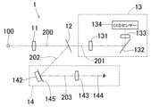
- FIG. 1 is a configuration diagram of a photometric device 1 according to the first embodiment of the present invention.
- the photometric device 1 includes an objective lens 11 that collects a light beam from an object 100 to be measured, and an aperture mirror (light beam) arranged behind the objective lens 11 (front in the traveling direction of the light beam 200). It includes a (corresponding to a dividing means) 12, a measuring optical system 13, and a finder optical system 14.
- the aperture mirror 12 is a mirror having an aperture through which the luminous flux 200 that has passed through the objective lens 11 passes through.
- the luminous flux 201 from the photometric area of the object to be measured 100 passes through the aperture of the aperture mirror 12 and goes straight to the measurement optical system 13 in the subsequent stage.
- the luminous flux outside the photometric area is reflected as the luminous flux 202 by the aperture mirror 12, passes through the lens group including the reflection mirror 141 and the relay lens 143 in the finder optical system 14, and then from the finder eyepiece 144 to the observer's pupil. Be guided.
- the observer visually recognizes the object to be measured 100 and the index circle (the area that is not reflected by the aperture mirror and looks black to the user) from the finder eyepiece 144, and performs measurement positioning and focusing.
- the measurement optical system 13 includes a condenser lens 131 that concentrates the light beam 201 that has passed through the opening of the aperture mirror 12, a diffraction grid 132 that disperses the light beam 201 that has passed through the condenser lens 131, and a front of the diffraction grid 132.
- An imaging lens 133 arranged (downstream side) and a CCD sensor (corresponding to a photometric means) 134 as a two-dimensional light receiving sensor that receives the diffracted light from the diffraction grid 132 via the imaging lens 133 are provided. ..
- the configuration of such a measurement optical system 13 is known.
- the light receiving sensor (corresponding to the light receiving means) 142 is arranged at a position on the optical path between the reflection mirror 141 and the relay lens 143 in the finder optical system 14 so that a part of the light flux 203 can be received. There is.
- the light receiving sensor 142 is preferably arranged at a position off the center of the index circle so as not to interfere with the observation in the index circle when the observer looks into the finder eyepiece 144.
- the luminous flux 200 focused from the object to be measured 100 through the objective lens 11 is the light flux 201 directed to the measurement optical system 13 and the finder optical system 14 by the aperture mirror 12. It is divided into a luminous flux 202 toward.
- the luminous flux 201 directed toward the measurement optical system 13 passes through the condenser lens 131, is separated by the diffraction grating 132 for each frequency component, and is imaged on the CCD sensor 134 via the imaging lens 133.
- the CCD sensor 134 generates an output for each spectroscopic frequency component. Based on this output, a photometric value is obtained by an arithmetic unit (not shown).
- the light beam 202 divided into the finder optical system 14 by the aperture mirror 12 is reflected by the reflection mirror 141 in the finder optical system 14. Then, a part of the reflected light flux 203 is received by the light receiving sensor 142, and the remaining light flux 203 passes through the relay lens 143 to reach the finder eyepiece 144 and further to the observer's pupil.
- the light receiving sensor-142 generates an output according to the light receiving result. This output is transmitted to a light emission profile analysis device (not shown) and used for analysis of a light emission profile including a light emission profile at extremely low brightness.
- the light receiving sensor 142 that generates the output for light emission profile analysis is located at a position where the light receiving sensor 142 is divided into the finder optical system 14 and further receives at least a part of the light beam 203 reflected by the reflection mirror. Since it is arranged, divided by the aperture mirror 12, and not arranged on the optical path that is incident on the measurement optical system 13 and guided to the CCD sensor 134, it emits light by the light receiving sensor 142 without being affected by the light measurement by the CCD sensor 134. Data for profile analysis can be acquired. Therefore, it is possible to perform photometry by the CCD sensor 134 and data acquisition for emission profile analysis by the light receiving sensor 142 in parallel, which is efficient.
- the light received by the light receiving sensor 142 can be received by using the aperture reflected light collected by the aperture mirror 12, it is possible to analyze the light emission profile at extremely low brightness.
- FIG. 2 is a block diagram of the photometric device 1 according to the second embodiment of the present invention.
- the arrangement position and the light receiving mode of the light receiving sensor 142 in the finder optical system 14 are different from those of the first embodiment shown in FIG.
- a half mirror 145 which transmits a part of the light beam 202 split into the finder optical system 14 by the aperture mirror 12 and reflects the remaining light, and is provided with a light receiving sensor 142. Is arranged at a position opposite to the light beam 202 of the half mirror 145 so as to receive at least a part of the light transmitted by the half mirror 145. Further, the luminous flux 203 reflected by the half mirror 145 is guided to the finder eyepiece portion 144.
- the light receiving sensor 142 that generates the output for light emission profile analysis is divided into the finder optical system 14 and further receives at least a part of the light transmitted by the half mirror 145. Since it is not arranged on the optical path that is divided by the aperture mirror 12 and is incident on the measurement optical system 13 and guided to the CCD sensor 134, it is not affected by the light measurement by the CCD sensor 134 and is not affected by the light receiving sensor 142. Data for luminescence profile analysis can be acquired. Therefore, it is possible to perform photometry by the CCD sensor 134 and data acquisition for emission profile analysis by the light receiving sensor 142 in parallel, which is efficient.
- FIG. 3 is a block diagram of the photometric device 1 according to the third embodiment of the present invention. This embodiment differs from the first embodiment shown in FIG. 1 in that the shutter 143 is provided in the vicinity of the light receiving sensor 142 in the finder optical system 14.
- the light receiving sensor 142 has a luminous flux 203 on the optical path between the reflection mirror 141 and the relay lens 143 in the finder optical system 14.
- a shutter 146 is provided close to the front side of the light receiving sensor 142 in the traveling direction of the light beam. The shutter 146 is for blocking back light incident from the finder eyepiece 144 when the light receiving sensor 142 receives light, in other words, when data for light emission profile analysis is output. For this reason, the shutter 146 is movable in the Y direction of FIG.
- the moving unit 150 blocks the optical path of the reverse light entering from the finder eyepiece portion 144.
- the shutter 146 is moved to the position where the shutter 146 is to be moved, and after the light is received by the light receiving sensor 142, the shutter is moved to the standby position at the bottom of FIG. 3 so as to be separated from the optical path.
- the light beam 202 divided into the finder optical system 14 by the aperture mirror 12 is reflected by the reflection mirror 141 in the finder optical system 14. Then, a part of the reflected light flux 203 is received by the light receiving sensor 142, and the remaining light flux 203 passes through the relay lens 143 and is guided to the finder eyepiece 144, and further reaches the observer's pupil.
- the shutter 146 that has been waiting in the standby position moves to the position where the reverse light from the finder eyepiece 144 is blocked by the moving unit 150, and waits again after receiving light from the light receiving sensor 142. Move to position.
- the light receiving sensor 142 receives light in a state where the reverse light from the finder eyepiece 144 is blocked by the shutter 146, and generates an output according to the light receiving result. This output is transmitted to a light emission profile analysis device (not shown) and used for analysis of a light emission profile including a light emission profile at extremely low brightness.
- the light receiving sensor 142 is arranged at a position where it is divided into the finder optical system 14 and receives a part of the light reaching the finder eyepiece 144, and further, the light receiving sensor 142 receives light. Occasionally, the back light from the viewfinder eyepiece 144 is blocked by the shutter 144. Therefore, it is possible to surely realize a configuration in which the light receiving sensor 142 is provided at a position where at least a part of the light divided into the finder optical system 14 is received, and the light measurement by the CCD sensor 134 and the light receiving sensor 142 are used. Data for emission profile analysis can be acquired in parallel. Further, when the light is received by the light receiving sensor 142, the adverse effect of the back light from the finder eyepiece 144 can be prevented by the shutter 146.
- the light receiving sensor 142 is fixedly arranged, and the shutter 146 is moved between the position where the back light from the finder eyepiece 144 is blocked and the standby position. did.
- the shutter 146 is placed between the position where the back light from the finder eyepiece 144 is blocked and the standby position. It may be configured to move with. In this case, by moving the shutter 146 on which the light receiving sensor 142 is mounted to a position where the reverse light is blocked according to the metering timing by the CCD sensor 134, the light is emitted from the light receiving sensor 142 in synchronization with the metering by the CCD sensor 134. You can get the output for profile analysis.
- a window that can be opened and closed is provided in the shutter 146, and the window is closed when the light receiving sensor 142 receives light to block the back light from the finder eyepiece 144. It may be configured to open the window.
- FIG. 4 is a block diagram of the photometric device 1 according to the fourth embodiment of the present invention.
- the shutter 146 is configured to be moved in the Y direction by the moving portion 150, but in the fourth embodiment, the light guide mirror 147 can be moved in the Y direction by the moving portion 150.
- the arrangement position of the light receiving sensor 142 is different from that of the third embodiment of FIG.
- the light guide mirror 147 is divided into the finder optical system 14 by the aperture mirror 12 and reflected by the reflection mirror 141 to the finder eyepiece 144 when the light receiving sensor 142 receives light, in other words, when data for light emission profile analysis is output. It serves to reflect at least a part of the luminous flux 203 and to block the back light from the finder eyepiece 144. Therefore, the light guide mirror 147 can be moved in the Y direction of FIG. 4 by the moving portion 150 in a state of being inclined diagonally downward with respect to the luminous flux 203 reflected by the reflection mirror 141 and reaching the finder eyepiece portion 144. It has been done.
- the moving unit 150 When the light receiving sensor 142 receives light, the moving unit 150 reflects at least a part of the luminous flux 203 reaching the finder eyepiece portion 144, and blocks the back light from the finder eyepiece portion 144, as shown in FIG.
- the light guide mirror 147 is moved to the reflection / cutoff position, which is the position where the light is received, while being tilted, and after the light is received by the light receiving sensor 142, it is moved to the standby position at the bottom of FIG. 4 to be separated from the optical path.
- the light receiving sensor 142 is arranged at a position where it receives at least a part of the light flux reflected diagonally downward by the light guide mirror 147 moved to the reflection / blocking position.
- the light beam 202 divided into the finder optical system 14 by the aperture mirror 12 is reflected by the reflection mirror 141 in the finder optical system 14 and guided to the finder eyepiece 144, and further, the observer. To the eyes of.
- the light guide mirror 147 that has been waiting in the standby position moves to the above-mentioned reflection / blocking position by the moving unit 150, and moves to the standby position again after receiving light from the light receiving sensor 142. ..
- the output for light emission profile analysis is acquired from the light receiving sensor 142 in synchronization with the photometric measurement by the CCD sensor 134. be able to.
- the luminous flux 203 is reflected by the light guide mirror 147 that has moved to the reflection / cutoff position, and the light receiving sensor 142 receives at least a part of the reflected light and generates an output according to the light receiving result.
- This output is transmitted to a light emission profile analysis device (not shown) and used for analysis of a light emission profile including a light emission profile at extremely low brightness.
- the light guide mirror 147 moved to the reflection / blocking position blocks the back light entering from the finder eyepiece 144 when the light receiving sensor 142 receives light.
- the light guide mirror 147 is divided into the finder optical system 14 from the standby position and reflects at least a part of the light flux 203 reaching the finder eyepiece 144. Then, the light guide mirror 142 moves to a reflection / blocking position that blocks the back light entering from the finder eyepiece 144, and the light receiving sensor 142 receives at least a part of the light reflected by the light guide mirror 147. With 147, it is possible to generate an output for light emission profile analysis from the light receiving sensor 142 while blocking the back light entering from the finder eyepiece 144 to prevent its adverse effect.
- FIG. 5 is a block diagram of the photometric device 1 according to the fifth embodiment of the present invention. This embodiment differs from the first embodiment shown in FIG. 1 in that the finder optical system 14 is provided with an electronic viewfinder 148.
- the light beam 202 divided into the finder optical system 14 by the aperture mirror 12 is directly incident on the electronic viewfinder 148, and the observer is measured on the screen of the electronic viewfinder 148. Observe the object 100 and the like.
- the electronic viewfinder 148 also serves as a light receiving sensor that generates an output for light emission profile analysis, and when light is received by the light receiving sensor, the output of the electronic viewfinder 148 is acquired as it is, and the output for light emission profile analysis is used. do.
- the component configuration can be simplified.
- the present invention is not limited to the above embodiment.
- the photometric device 1 is a spectroscopic device, that is, when the measurement optical system 13 is in a state where the light beam 201 passing through the condenser lens 131 is separated by the diffraction grating 132 and the photometry is performed by the CCD sensor 134.
- a photometric device of a type that measures light without spectroscopy may be used.
- the present invention can be used as a photometric device capable of performing data acquisition and photometry for analysis of a light emission profile in parallel.
- Photometer 11 Objective lens 12 Aperture mirror 13 Measurement optical system 14 Finder optical system 100 Object to be measured 132 Diffraction grating 134 CCD sensor (measurement means) 141 Reflective mirror 142 Light receiving sensor (light receiving means) 144 Finder eyepiece 145 Half mirror 146 Shutter 147 Light guide mirror 148 Electronic viewfinder 150 Moving part
Landscapes
- Physics & Mathematics (AREA)
- Spectroscopy & Molecular Physics (AREA)
- General Physics & Mathematics (AREA)
- Photometry And Measurement Of Optical Pulse Characteristics (AREA)
- Exposure Control For Cameras (AREA)
Priority Applications (3)
| Application Number | Priority Date | Filing Date | Title |
|---|---|---|---|
| CN202180058760.6A CN116057359A (zh) | 2020-08-03 | 2021-07-14 | 测光装置 |
| US18/019,231 US12031860B2 (en) | 2020-08-03 | 2021-07-14 | Photometer |
| JP2022541182A JPWO2022030201A1 (https=) | 2020-08-03 | 2021-07-14 |
Applications Claiming Priority (2)
| Application Number | Priority Date | Filing Date | Title |
|---|---|---|---|
| JP2020-131729 | 2020-08-03 | ||
| JP2020131729 | 2020-08-03 |
Publications (1)
| Publication Number | Publication Date |
|---|---|
| WO2022030201A1 true WO2022030201A1 (ja) | 2022-02-10 |
Family
ID=80119789
Family Applications (1)
| Application Number | Title | Priority Date | Filing Date |
|---|---|---|---|
| PCT/JP2021/026393 Ceased WO2022030201A1 (ja) | 2020-08-03 | 2021-07-14 | 測光装置 |
Country Status (4)
| Country | Link |
|---|---|
| US (1) | US12031860B2 (https=) |
| JP (1) | JPWO2022030201A1 (https=) |
| CN (1) | CN116057359A (https=) |
| WO (1) | WO2022030201A1 (https=) |
Citations (8)
| Publication number | Priority date | Publication date | Assignee | Title |
|---|---|---|---|---|
| JP2005221651A (ja) * | 2004-02-04 | 2005-08-18 | Konica Minolta Sensing Inc | 測光装置 |
| JP2012016620A (ja) * | 2011-10-24 | 2012-01-26 | Topcon Corp | 眼底観察装置 |
| JP2012198119A (ja) * | 2011-03-22 | 2012-10-18 | Olympus Corp | 測光装置および測光方法 |
| JP2013507612A (ja) * | 2009-10-12 | 2013-03-04 | ベンタナ メディカル システムズ, インコーポレイテッド | 高められた病理学的決定のための複数モダリティコントラストおよび明視野コンテキスト表現、および組織内の複数検体検出 |
| US20160238532A1 (en) * | 2013-06-21 | 2016-08-18 | Invenio Imaging Inc. | Multi-photon systems and methods |
| WO2017179520A1 (ja) * | 2016-04-14 | 2017-10-19 | コニカミノルタ株式会社 | 光学測定装置、故障判断システム、故障判断方法、および故障判断プログラム |
| JP2018529980A (ja) * | 2015-08-07 | 2018-10-11 | センチネル モニタリング システムズ インコーポレイテッド | オンラインプロセスモニタリング |
| WO2019021472A1 (ja) * | 2017-07-28 | 2019-01-31 | オリンパス株式会社 | 細胞特定方法、細胞集団の製造方法及び細胞特定システム |
Family Cites Families (6)
| Publication number | Priority date | Publication date | Assignee | Title |
|---|---|---|---|---|
| US3813172A (en) * | 1972-01-03 | 1974-05-28 | Kollmorgen Corp | Photometric device with a plurality of measuring fields |
| US3740147A (en) * | 1972-01-10 | 1973-06-19 | Farrand Optical Co Inc | Microspectrophotometer with two fields of view |
| US20050103979A1 (en) * | 2003-11-13 | 2005-05-19 | Photo Research, Inc. | Temporal source analysis using array detectors |
| CN101799324A (zh) * | 2009-12-15 | 2010-08-11 | 杭州远方光电信息有限公司 | 一种亮度计 |
| CN101813517B (zh) * | 2009-12-23 | 2013-09-18 | 杭州远方光电信息股份有限公司 | 一种亮度测量装置 |
| JP5928308B2 (ja) * | 2012-11-13 | 2016-06-01 | ソニー株式会社 | 画像取得装置および画像取得方法 |
-
2021
- 2021-07-14 JP JP2022541182A patent/JPWO2022030201A1/ja active Pending
- 2021-07-14 WO PCT/JP2021/026393 patent/WO2022030201A1/ja not_active Ceased
- 2021-07-14 US US18/019,231 patent/US12031860B2/en active Active
- 2021-07-14 CN CN202180058760.6A patent/CN116057359A/zh active Pending
Patent Citations (8)
| Publication number | Priority date | Publication date | Assignee | Title |
|---|---|---|---|---|
| JP2005221651A (ja) * | 2004-02-04 | 2005-08-18 | Konica Minolta Sensing Inc | 測光装置 |
| JP2013507612A (ja) * | 2009-10-12 | 2013-03-04 | ベンタナ メディカル システムズ, インコーポレイテッド | 高められた病理学的決定のための複数モダリティコントラストおよび明視野コンテキスト表現、および組織内の複数検体検出 |
| JP2012198119A (ja) * | 2011-03-22 | 2012-10-18 | Olympus Corp | 測光装置および測光方法 |
| JP2012016620A (ja) * | 2011-10-24 | 2012-01-26 | Topcon Corp | 眼底観察装置 |
| US20160238532A1 (en) * | 2013-06-21 | 2016-08-18 | Invenio Imaging Inc. | Multi-photon systems and methods |
| JP2018529980A (ja) * | 2015-08-07 | 2018-10-11 | センチネル モニタリング システムズ インコーポレイテッド | オンラインプロセスモニタリング |
| WO2017179520A1 (ja) * | 2016-04-14 | 2017-10-19 | コニカミノルタ株式会社 | 光学測定装置、故障判断システム、故障判断方法、および故障判断プログラム |
| WO2019021472A1 (ja) * | 2017-07-28 | 2019-01-31 | オリンパス株式会社 | 細胞特定方法、細胞集団の製造方法及び細胞特定システム |
Also Published As
| Publication number | Publication date |
|---|---|
| JPWO2022030201A1 (https=) | 2022-02-10 |
| US20230273067A1 (en) | 2023-08-31 |
| US12031860B2 (en) | 2024-07-09 |
| CN116057359A (zh) | 2023-05-02 |
Similar Documents
| Publication | Publication Date | Title |
|---|---|---|
| US8390926B2 (en) | High speed acquisition vision system and method for selectively viewing object features | |
| US12298221B2 (en) | Observation device | |
| CN120446068A (zh) | 测序拍照成像系统及测序拍照成像方法 | |
| CN102419473A (zh) | 摄影方法和显微镜装置 | |
| JP2012244277A (ja) | 撮像装置およびこれを備える顕微鏡システム | |
| EP3893039A1 (en) | Oblique plane microscope for imaging a sample | |
| US11846544B2 (en) | Spectrophotometer | |
| CN115266578A (zh) | 分析装置 | |
| US20240094518A1 (en) | Microscope for fluorescence light imaging | |
| CN113671717B (zh) | 光源装置和光学检测设备 | |
| WO2022030201A1 (ja) | 測光装置 | |
| CN117233947B (zh) | 显微镜照明系统、控制方法及显微成像检测系统 | |
| JP4262380B2 (ja) | 光量測定装置 | |
| US12146787B2 (en) | Optical control apparatus and optical control method | |
| JPH0580246A (ja) | 自動合焦装置及びそれを備えた観察装置 | |
| EP4060977B1 (en) | An arrangement for assessing ambient light in a video camera | |
| RU2464608C1 (ru) | Оптическая система голографической видеокамеры | |
| JP2007285761A (ja) | ハーフミラーおよびそれを使用した顕微分光測定装置 | |
| KR20260015745A (ko) | 광학 장치 및 광학 장치의 제어 방법 | |
| JP3447877B2 (ja) | 濃度計測光学系 | |
| US7868279B2 (en) | Focus detecting apparatus for focusing on surface of transparent substance | |
| JP2923328B2 (ja) | 顕微鏡写真撮影装置 | |
| JPH11271632A (ja) | 顕微鏡 | |
| CN117031718A (zh) | 一种基于光谱和偏振联合调制的无标记显微成像装置 | |
| JP2007183111A (ja) | 光強度検出装置とこれを有する光学装置、顕微鏡 |
Legal Events
| Date | Code | Title | Description |
|---|---|---|---|
| 121 | Ep: the epo has been informed by wipo that ep was designated in this application |
Ref document number: 21854600 Country of ref document: EP Kind code of ref document: A1 |
|
| ENP | Entry into the national phase |
Ref document number: 2022541182 Country of ref document: JP Kind code of ref document: A |
|
| NENP | Non-entry into the national phase |
Ref country code: DE |
|
| 122 | Ep: pct application non-entry in european phase |
Ref document number: 21854600 Country of ref document: EP Kind code of ref document: A1 |