WO2022029941A1 - 光モジュール - Google Patents
光モジュール Download PDFInfo
- Publication number
- WO2022029941A1 WO2022029941A1 PCT/JP2020/030090 JP2020030090W WO2022029941A1 WO 2022029941 A1 WO2022029941 A1 WO 2022029941A1 JP 2020030090 W JP2020030090 W JP 2020030090W WO 2022029941 A1 WO2022029941 A1 WO 2022029941A1
- Authority
- WO
- WIPO (PCT)
- Prior art keywords
- optical
- protrusion
- optical module
- fiber
- optical fiber
- Prior art date
- Legal status (The legal status is an assumption and is not a legal conclusion. Google has not performed a legal analysis and makes no representation as to the accuracy of the status listed.)
- Ceased
Links
Images



Classifications
-
- G—PHYSICS
- G02—OPTICS
- G02B—OPTICAL ELEMENTS, SYSTEMS OR APPARATUS
- G02B6/00—Light guides; Structural details of arrangements comprising light guides and other optical elements, e.g. couplings
- G02B6/24—Coupling light guides
- G02B6/26—Optical coupling means
- G02B6/30—Optical coupling means for use between fibre and thin-film device
-
- G—PHYSICS
- G02—OPTICS
- G02B—OPTICAL ELEMENTS, SYSTEMS OR APPARATUS
- G02B6/00—Light guides; Structural details of arrangements comprising light guides and other optical elements, e.g. couplings
- G02B6/24—Coupling light guides
- G02B6/36—Mechanical coupling means
- G02B6/3616—Holders, macro size fixtures for mechanically holding or positioning fibres, e.g. on an optical bench
- G02B6/362—Vacuum holders for optical elements
-
- G—PHYSICS
- G02—OPTICS
- G02B—OPTICAL ELEMENTS, SYSTEMS OR APPARATUS
- G02B6/00—Light guides; Structural details of arrangements comprising light guides and other optical elements, e.g. couplings
- G02B6/44—Mechanical structures for providing tensile strength and external protection for fibres, e.g. optical transmission cables
- G02B6/4439—Auxiliary devices
- G02B6/444—Systems or boxes with surplus lengths
Definitions
- the present invention relates to an optical module which is an optical communication component that transmits and processes high-frequency electric signals and optical signals.
- BGA Ball Grid Array
- the BGA package is mounted on the board by reflow mounting. Therefore, it can be expected that the mounting cost will be reduced as compared with the case where the side-mounted pin package and the flexible printed wiring board (FPC) package used in the conventional optical module are mounted by soldering.
- FPC flexible printed wiring board
- the optical module with an optical fiber has a configuration in which the optical fiber is optically coupled to the optical waveguide chip built in the optical device.
- the optical module with an optical fiber has a configuration in which the optical fiber is optically coupled to the optical waveguide chip built in the optical device.
- Patent Document 1 there is a technique (see Patent Document 1) in which an optical fiber is wound and attached to an optical fiber extra length storage portion provided in the middle of each receptacle between a receptacle configuration surface and an optical circuit arrangement surface while rotating the optical fiber in a coil shape. Proposed. Further, there is known a technique of pressing an optical fiber against a wall structure provided in a housing of an optical connector or a grip portion of an optical fiber and accommodating the optical fiber by the restoring force of the optical fiber (see Patent Document 2). The technique of storing the optical fiber coupled to the optical device using the latter wall structure is easier to store the optical fiber than the case of attaching the optical fiber to the optical fiber extra length storage portion while rotating the optical fiber. It is attracting attention because of its convenience.
- FIG. 1 is a schematic view showing the basic structure of the optical module 600 using the conventional wall structure.
- FIG. 1A is a top view of the optical module 600.
- FIG. 1B is a side view of the optical module 600.
- FIG. 1 (c) is an end view of the optical module 600 in a cross section in the Ic-Ic direction in FIG. 1 (a).
- the optical module 600 has a structure in which an optical device 100 with an optical fiber 300 is attached to and mounted on a fiber holding carrier 400 having a flat plate-shaped substrate.
- the optical device 100 incorporates, for example, an optical IC chip 200 as an optical waveguide chip, and an optical fiber 300 is optically coupled to the optical IC chip 200 so as to be connected and held.
- a pair of wall portions 410 are erected on the upper surface side of the fiber holding carrier 400 so as to face each other near the long edge thereof, and the optical device 100 is attached and fixed to the lower surface side of the fiber holding carrier 400. Will be done.
- the extra length portion of the optical fiber 300 extending from the optical device 100 is routed between the pair of wall portions 410 and stored.
- the extra length portion of the optical fiber 300 is fixed between the pair of wall portions 410 by the restoring force of the optical fiber 300 when the optical fiber 300 is pressed against the pair of wall portions 410.
- the pickup region EP shown by a circular dotted line in the center of the upper surface of the fiber holding carrier 400 shown in FIG. 1A is automatically adsorbed by a device on which the optical module 600 is mounted for surface mounting. , Used for transporting.
- the extra length portion is made smaller on the opposite surface (upper surface) side of the fiber holding carrier 400 to which the optical device 100 is attached. Can be stored. Therefore, the pickup region EP in the central portion on the upper surface side of the fiber holding carrier 400 can be used and automatically adsorbed and conveyed by the mounting device.
- the pickup area EP is adsorbed by a pickup tool or the like of the on-board device.
- An object of the embodiment of the present invention is to provide an optical module having a structure capable of preventing an extra length portion of an optical fiber to be housed from entering a pickup region for mounting a component.
- one aspect of the present invention is an optical device including an optical waveguide chip, an optical fiber optically coupled to the optical waveguide chip, and an optical device attached to the optical device to provide a pickup region for light.
- An optical module including a fiber holding carrier for holding a fiber, characterized in that the fiber holding carrier is provided with a protrusion for preventing the optical fiber from entering the pickup region.
- an optical module having a structure capable of preventing the optical fiber from entering the pickup region for automatic adsorption by the on-board device.
- FIG. 1 It is a schematic diagram which showed the basic structure of the optical module using the conventional wall structure.
- FIG. 1 is a top view of an optical module.
- B is a side view of an optical module.
- C is a cross-sectional view of the optical module in the Ic-Ic direction in (a). It is a schematic diagram which showed the basic structure of the optical module which concerns on Embodiment 1 of this invention.
- (A) is a top view of an optical module.
- (B) is a side view of an optical module.
- (C) is an end view of the optical module in the direction of IIc-IIc in (a). It is a schematic diagram which showed the basic structure of the optical module which concerns on Embodiment 2 of this invention.
- (A) is a top view of an optical module.
- (B) is a side view of an optical module.
- (C) is a cross-sectional view of the optical module in the direction of IIIc-IIIc in (a). It is a schematic diagram which showed the basic structure of the optical module which concerns on Embodiment 3 of this invention.
- (A) is a top view of an optical module.
- (B) is a side view of an optical module.
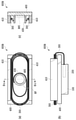
- FIG. 2 is a schematic view showing the basic structure of the optical module 600A according to the first embodiment of the present invention.
- FIG. 2A is a top view of the optical module 600A.
- FIG. 2B is a side view of the optical module 600A.
- FIG. 2C is an end view of the optical module 600A in the direction of IIc-IIc in FIG. 2A.
- optical device 100 with the optical fiber 300 is attached to and mounted on the fiber holding carrier 400 having a flat plate-shaped substrate. It has become.
- the optical device 100 has a built-in optical IC chip 200, and the optical fiber 300 is optically coupled to the optical IC chip 200 so as to be connected and held.
- a pair of wall portions 410 are erected on the upper surface side of the fiber holding carrier 400 so as to face each other near the long edge thereof, and the optical device 100 is attached and fixed to the lower surface side of the fiber holding carrier 400. Will be done.
- a cylindrical protrusion portion having a circular region substantially in the center of the upper surface of the fiber holding carrier 400 and having a dedicated pickup region EP1 secured in the entire pickup region EP for automatic suction by the mounting device.
- the protrusion 420 has the same height as the pair of wall portions 410 in the direction perpendicular to the pickup region EP, and has a flat top surface 420a at the top in the height.
- the surface 420a is the dedicated pickup area EP1.
- the top surface 420a of the protrusion 420 is used as the pickup region EP1 that replaces the existing pickup region EP.
- the pickup region EP1 is located directly above the pickup region EP on the upper surface of the fiber holding carrier 400 and has the same area. Therefore, the top surface 420a of the protrusion 420 has a flat structure sufficient for picking up. That is, again, the pickup region EP1 is used for mounting the optical module 600A for surface mounting and automatically sucking and transporting the optical module 600A by the mounting device.
- the optical device 100 be attached to the fiber holding carrier 400 in an adhesive structure from the viewpoint of ease of removal and configuration. Further, instead of the adhesive structure, an optical device other than the carrier or the optical device 100, or a mechanical clamp structure provided on another member may be applied.
- a pair of facing wall portions 410 are provided on the surface of the fiber holding carrier 400 opposite to the surface on which the optical device 100 is attached. Therefore, in the state after the optical device 100 is attached to the fiber holding carrier 400, the extra length portion of the optical fiber 300 extending from the optical device 100 is routed between the pair of wall portions 410 and stored. At this time, the extra length portion including the tip portion of the optical fiber 300 is held in the storage area of the fiber holding carrier 400 by the restoring force generated by being pressed against the pair of wall portions 410. Further, in this holding state, the tip portion of the extra length portion of the optical fiber 300 can be arranged along the outer periphery of the protrusion 420. As a result, the extra length portion including the tip portion of the optical fiber 300 is compactly housed and fixed between the pair of wall portions 410 and the protrusions 420.
- the extra length portion is the opposite surface (upper surface) of the fiber holding carrier 400 to which the optical device 100 is attached. Can be miniaturized and stored on the side. Therefore, the top surface 420a of the protrusion 420 in the central portion on the upper surface side of the fiber holding carrier 400 can be used as the pickup region EP1 and can be automatically adsorbed and conveyed by the mounting device.
- the pickup area EP1 here is also attracted by the pickup tool or the like of the on-board device.
- a cylindrical protrusion 420 is provided on the entire existing pickup region EP on the upper surface of the fiber holding carrier 400, and the top surface 420a of the protrusion 420 is used as a dedicated pickup region EP1.
- the outer peripheral wall of the protrusion 420 allows the tip portion of the extra length portion of the optical fiber 300 to enter the dedicated pickup area EP1. Intrusion can be effectively prevented. As a result, it is possible to sufficiently prevent the tip portion of the extra length portion of the optical fiber 300 from entering the dedicated pickup region EP1 for automatic suction by the mounting device.
- the wall structure of the protrusion 420 has a cylindrical shape is shown.
- the extra length portion of the optical fiber 300 is also a dedicated pickup. It is possible to prevent the region EP1 from invading.
- the protrusion it is desirable that the portion 420 has a cylindrical shape.
- FIG. 3 is a schematic view showing the basic structure of the optical module 600B according to the second embodiment of the present invention.
- FIG. 3A is a top view of the optical module 600B.
- FIG. 3B is a side view of the optical module 600B.
- FIG. 3 (c) is an end view of the optical module 600B in the direction of IIIc-IIIc in FIG. 3 (a).
- a hollow cylindrical protrusion 430 is provided on the peripheral edge of the pickup region EP instead of the cylindrical protrusion 420 of the optical module 600A. It is provided. Then, as shown in FIGS. 3A and 3C, a dedicated pickup region EP2 is secured inside the cylindrical protrusion 430 on the upper surface of the fiber holding carrier 400. Since the dedicated pickup area EP2 has a smaller area than the pickup area EP due to the presence of the hollow cylindrical protrusion 430, it is sufficiently flattened so that it can receive the suction force required for vacuum suction. Must have been.
- the dedicated pickup region EP2 can be regarded as the pickup region EP corresponding to the hollow portion in the cylindrical protrusion 430 of the wall structure.
- the hollow cylindrical protrusion 430 has the same height as the pair of wall portions 410 in the direction perpendicular to the pickup region EP.
- Other components of the optical module 600B are the same as those of the optical module 600A.
- the hollow cylindrical protrusion 430 is effective when the fiber holding carrier 400 is manufactured by resin molding.
- the reason is that when a wall structure having a cylindrical protrusion 420 is created by resin molding as in the case of the first embodiment, the cylindrical protrusion 420 due to the difference in the thickness of the wall structure between the protrusion 420 and the wall 410.
- a depression may be formed on the top surface 420a of the surface. If a depression is formed on the top surface 420a of the protrusion 420, the flatness may be impaired and problems such as poor adsorption and dropping during transportation may occur.
- the dedicated pickup area EP2 is partitioned by the presence of the hollow cylindrical protrusion 430, but basically the area of the existing pickup area EP is narrowed, so that the protrusion is formed. It is not easily affected by the formation of 430.
- the extra length portion is the opposite surface (upper surface) of the fiber holding carrier 400 to which the optical device 100 is attached.
- the tip portion of the extra length portion of the optical fiber 300 is arranged along the outer periphery of the protrusion 430. Therefore, the hollow portion inside the protrusion 430 in the central portion on the upper surface side of the fiber holding carrier 400 is used as the pickup region EP2, and can be automatically adsorbed and conveyed by the mounting device.
- the pickup area EP2 here is also attracted by the pickup tool or the like of the on-board device.
- a hollow cylindrical protrusion 430 is provided on the peripheral edge of the existing pickup region EP on the upper surface of the fiber holding carrier 400, and the inside of the protrusion 430 is dedicated to the pickup region EP2. It is supposed to be. Therefore, even if an impact is applied from the outside and the storage position of the optical fiber 300 changes to some extent, the outer peripheral wall of the protrusion 430 allows the tip portion of the extra length portion of the optical fiber 300 to enter the dedicated pickup area EP2. Intrusion can be effectively prevented. As a result, it is possible to sufficiently prevent the tip portion of the extra length portion of the optical fiber 300 from entering the dedicated pickup region EP2 for automatic suction by the mounting device.
- FIG. 4 is a schematic view showing the basic structure of the optical module 100C according to the third embodiment of the present invention.
- FIG. 4A is a top view of the optical module 100C.
- FIG. 4B is a side view of the optical module 100C.
- the peripheral portion of the pickup region EP has a cylindrical local shape separated by four cuts 450.
- Four protrusions 440 are provided.
- a dedicated pickup region EP2 is secured inside each protrusion 440 having a cylindrical local shape on the upper surface of the fiber holding carrier 400.
- the dedicated pickup area EP2 also has a smaller area than the pickup area EP due to the presence of each protrusion 440 having a cylindrical local shape, and is therefore sufficiently flat so that the suction force required for vacuum suction can be received. It needs to be made.
- Each protrusion 440 having a cylindrical local shape has the same height as the pair of wall portions 410 in the direction perpendicular to the pickup region EP.
- Other components of the optical module 600C are the same as those of the optical module 600A.
- Each protrusion 440 having a cylindrical local shape is effective when the optical device 100 is adhesively fixed to the fiber holding carrier 400.
- the reason is that after the optical module 600C is surface-mounted, when the fiber holding carrier 400 is removed, the fiber holding carrier 400 can be removed by entwining the protrusion portion of another jig with the cut 450 and rotating the carrier 400. Because. As a result, the removal work that does not depend on the manual work of the worker becomes possible, and the convenience is enhanced.
- this optical module 100C a configuration has been described in which four cuts 450 are provided in a cross shape and four cylindrical locally shaped protrusions 440 are provided. However, if the number is such that rotation removal work is possible, other than that. You may apply the number of.
- the extra length portion is the opposite surface of the fiber holding carrier 400 to which the optical device 100 is attached. Can be miniaturized and stored on the upper surface) side.
- the tip portion of the extra length portion of the optical fiber 300 the tip portion of the surplus length portion of the optical fiber 300 is arranged along the outer periphery of the protrusion 440. Therefore, the hollow portion inside each protrusion 440 in the central portion on the upper surface side of the fiber holding carrier 400 is used as the pickup region EP2, and can be automatically adsorbed and conveyed by the mounting device.
- the pickup area EP2 here is also attracted by the pickup tool or the like of the on-board device.
- each protrusion 440 having a cylindrical local shape is provided on the peripheral portion of the existing pickup region EP on the upper surface of the fiber holding carrier 400, and the inside of each protrusion 440 is a dedicated pickup region. It is EP2. Therefore, even if an impact is applied from the outside and the storage position of the optical fiber 300 changes to some extent, the outer peripheral wall of each protrusion 440 enters the dedicated pickup area EP2 at the tip of the extra length portion of the optical fiber 300. Can be effectively prevented from invading. As a result, it is possible to sufficiently prevent the tip portion of the extra length portion of the optical fiber 300 from entering the dedicated pickup area EP2 for mounting the component.
- the wall structure in which the extra length portion of the optical fiber 300 is pressed against the pair of wall portions 410 and is stored in a small size is shown.
- the optical fiber 300 is sandwiched between the groove structures. It may be configured to store the extra length part of.
- a claw structure may be provided for this purpose. In this case, the claw structure is provided in the direction perpendicular to the height direction of the wall portion 410.
- a configuration in which one long optical fiber 300 is connected to the optical IC chip 200 is illustrated.
- a plurality of optical fibers 300 are connected to the optical IC chip 200, and the extra length portion of each optical fiber 300 is accommodated in the extra length portion of each optical fiber 300 on the upper surface of the fiber holding carrier 400. It may be configured to be stored in. However, in this case, the plurality of optical fibers 300 can be exemplified for use in applications such as input light, transmission light, reception light, and input light having different wavelengths for wavelength division multiplexing.
- the configuration in which the protrusion 420 is provided on the entire pickup region EP arranged in the center of the upper surface of the fiber holding carrier 400 has been described.
- the configuration in which the protrusion 430 and each protrusion 440 are provided on the peripheral edge of the same pickup region EP has been described.
- alternative structures can also be applied.
- the pickup region EP may not be the central portion depending on the position where the optical device 100 is arranged on the fiber holding carrier 400 and the design of the center of gravity position due to the structure of the fiber holding carrier 400.
- a plurality of pickup area EPs may be arranged depending on the shape of the pickup tool and the convenience of process design.
- a configuration is applied in which the protrusions 420 are provided on the entire pickup area EP or each pickup area EP other than the central portion, or the protrusions 430 and each protrusion 440 are provided on the peripheral edges of the pickup area EP and each pickup area EP. can.
- the case where the height of the protrusions 420, 430 and the protrusions 440 in the direction perpendicular to the pickup region EP is the same as the height of the wall portion 410 has been described, but the wall portion 410 has been described. It may be taller than. Further, the height of the region where the extra length portion of the optical fiber 300 on the upper surface of the fiber holding carrier 400 is housed is designed to be lower than the height of the wall portion 410 due to the claw structure provided on the wall portion 410 or the like. In some cases.
- the height of the protrusions 420, 430, and each protrusion 440 in the direction perpendicular to the pickup area EP is designed to be higher than the height of the area where the extra length portion of the optical fiber 300 is housed. I just need to be there.
Landscapes
- Physics & Mathematics (AREA)
- General Physics & Mathematics (AREA)
- Optics & Photonics (AREA)
- Optical Couplings Of Light Guides (AREA)
- Light Guides In General And Applications Therefor (AREA)
Abstract
Description
図2は、本発明の実施形態1に係る光モジュール600Aの基本構造を示した概略図である。図2(a)は、光モジュール600Aの上面図である。図2(b)は、光モジュール600Aの側面図である。図2(c)は、光モジュール600Aの図2(a)中のIIc-IIc方向で断面にした端面図である。
図3は、本発明の実施形態2に係る光モジュール600Bの基本構造を示した概略図である。図3(a)は、光モジュール600Bの上面図である。図3(b)は、光モジュール600Bの側面図である。図3(c)は、光モジュール600Bの図3(a)中のIIIc-IIIc方向で断面にした端面図である。
図4は、本発明の実施形態3に係る光モジュール100Cの基本構造を示した概略図である。図4(a)は、光モジュール100Cの上面図である。図4(b)は、光モジュール100Cの側面図である。
Claims (8)
- 光導波路チップを含む光デバイスと、
前記光導波路チップに光学的に結合された光ファイバと、
前記光デバイスに取り付けられ、ピックアップ領域が設けられて前記光ファイバを保持するファイバ保持用キャリアと、
を備えた光モジュールであって、
前記ファイバ保持用キャリアに、前記光ファイバが前記ピックアップ領域内に侵入することを防止する突起部が設けられたことを特徴とする光モジュール。 - 前記突起部は、突起方向の頂部に前記ピックアップ領域を有する
ことを特徴とする請求項1に記載の光モジュール。 - 前記突起部は、突起方向に延在する中空部を有する筒形状の壁構造であり、当該筒形状の底部に前記ピックアップ領域を有する
ことを特徴とする請求項1に記載の光モジュール。 - 前記壁構造には、切れ目が設けられている
ことを特徴とする請求項3に記載の光モジュール。 - 前記切れ目は、複数設けられて前記突起部が複数個存在する
ことを特徴とする請求項4に記載の光モジュール。 - 前記ピックアップ領域は、円形状である
ことを特徴とする請求項1~5の何れか1項に記載の光モジュール。 - 前記ファイバ保持用キャリアの前記光デバイスを取り付けた面とは反対の面には、複数の壁部が設けられており、
前記光ファイバは、余長部分が前記複数の壁部に押し当てられることによる復元力で前記ファイバ保持用キャリアの収納領域となる当該複数の壁部と前記突起部との間に保持され、且つ当該余長部分での先端部分が当該突起部の外周に沿うように配置された
ことを特徴とする請求項1~6の何れか1項に記載の光モジュール。 - 前記突起部における前記ピックアップ領域と垂直な方向での背高は、前記光ファイバの余長部分が収納される領域の背高よりも高い
ことを特徴とする請求項7に記載の光モジュール。
Priority Applications (3)
| Application Number | Priority Date | Filing Date | Title |
|---|---|---|---|
| PCT/JP2020/030090 WO2022029941A1 (ja) | 2020-08-05 | 2020-08-05 | 光モジュール |
| JP2022541027A JP7364967B2 (ja) | 2020-08-05 | 2020-08-05 | 光モジュール |
| US18/005,141 US12248181B2 (en) | 2020-08-05 | 2020-08-05 | Optical module |
Applications Claiming Priority (1)
| Application Number | Priority Date | Filing Date | Title |
|---|---|---|---|
| PCT/JP2020/030090 WO2022029941A1 (ja) | 2020-08-05 | 2020-08-05 | 光モジュール |
Publications (1)
| Publication Number | Publication Date |
|---|---|
| WO2022029941A1 true WO2022029941A1 (ja) | 2022-02-10 |
Family
ID=80117805
Family Applications (1)
| Application Number | Title | Priority Date | Filing Date |
|---|---|---|---|
| PCT/JP2020/030090 Ceased WO2022029941A1 (ja) | 2020-08-05 | 2020-08-05 | 光モジュール |
Country Status (3)
| Country | Link |
|---|---|
| US (1) | US12248181B2 (ja) |
| JP (1) | JP7364967B2 (ja) |
| WO (1) | WO2022029941A1 (ja) |
Cited By (1)
| Publication number | Priority date | Publication date | Assignee | Title |
|---|---|---|---|---|
| JP7741930B1 (ja) * | 2024-05-30 | 2025-09-18 | Nttイノベーティブデバイス株式会社 | 光モジュールカバー部品、光モジュール保持部品及び光モジュール組立部品 |
Citations (6)
| Publication number | Priority date | Publication date | Assignee | Title |
|---|---|---|---|---|
| JPH04191705A (ja) * | 1990-11-26 | 1992-07-10 | Fujitsu Ltd | 光ファイバケーブルの余長収納装置 |
| JP2007156117A (ja) * | 2005-12-06 | 2007-06-21 | Nec Corp | 光ファイバ損失調整方法、光ファイバ損失調整装置及び光伝送システム |
| US20160124164A1 (en) * | 2014-10-29 | 2016-05-05 | Acacia Communications, Inc. | Optoelectronic ball grid array package with fiber |
| US10025047B1 (en) * | 2017-04-14 | 2018-07-17 | Google Llc | Integration of silicon photonics IC for high data rate |
| JP2019191421A (ja) * | 2018-04-26 | 2019-10-31 | 日本電信電話株式会社 | 光モジュール |
| JP2020112654A (ja) * | 2019-01-10 | 2020-07-27 | 日本電信電話株式会社 | 光モジュール |
Family Cites Families (3)
| Publication number | Priority date | Publication date | Assignee | Title |
|---|---|---|---|---|
| US6290401B1 (en) * | 1999-04-26 | 2001-09-18 | Corning Incorporated | Automated chip/phaser holder |
| JP4210268B2 (ja) | 2005-05-11 | 2009-01-14 | 日本電信電話株式会社 | 光モジュール |
| JP5363514B2 (ja) | 2011-01-31 | 2013-12-11 | 日本電信電話株式会社 | 光コネクタ |
-
2020
- 2020-08-05 JP JP2022541027A patent/JP7364967B2/ja active Active
- 2020-08-05 WO PCT/JP2020/030090 patent/WO2022029941A1/ja not_active Ceased
- 2020-08-05 US US18/005,141 patent/US12248181B2/en active Active
Patent Citations (6)
| Publication number | Priority date | Publication date | Assignee | Title |
|---|---|---|---|---|
| JPH04191705A (ja) * | 1990-11-26 | 1992-07-10 | Fujitsu Ltd | 光ファイバケーブルの余長収納装置 |
| JP2007156117A (ja) * | 2005-12-06 | 2007-06-21 | Nec Corp | 光ファイバ損失調整方法、光ファイバ損失調整装置及び光伝送システム |
| US20160124164A1 (en) * | 2014-10-29 | 2016-05-05 | Acacia Communications, Inc. | Optoelectronic ball grid array package with fiber |
| US10025047B1 (en) * | 2017-04-14 | 2018-07-17 | Google Llc | Integration of silicon photonics IC for high data rate |
| JP2019191421A (ja) * | 2018-04-26 | 2019-10-31 | 日本電信電話株式会社 | 光モジュール |
| JP2020112654A (ja) * | 2019-01-10 | 2020-07-27 | 日本電信電話株式会社 | 光モジュール |
Cited By (2)
| Publication number | Priority date | Publication date | Assignee | Title |
|---|---|---|---|---|
| JP7741930B1 (ja) * | 2024-05-30 | 2025-09-18 | Nttイノベーティブデバイス株式会社 | 光モジュールカバー部品、光モジュール保持部品及び光モジュール組立部品 |
| WO2025249391A1 (ja) * | 2024-05-30 | 2025-12-04 | Nttイノベーティブデバイス株式会社 | 光モジュールカバー部品、光モジュール保持部品及び光モジュール組立部品 |
Also Published As
| Publication number | Publication date |
|---|---|
| US12248181B2 (en) | 2025-03-11 |
| JPWO2022029941A1 (ja) | 2022-02-10 |
| US20230258872A1 (en) | 2023-08-17 |
| JP7364967B2 (ja) | 2023-10-19 |
Similar Documents
| Publication | Publication Date | Title |
|---|---|---|
| US20050175297A1 (en) | Optical sub-assembly for opto-electronic modules | |
| US9104000B2 (en) | Optical module | |
| WO2020145260A1 (ja) | 光モジュール | |
| JP2003503858A (ja) | 光子デバイス用気密形チップスケールパッケージ | |
| JP2004354532A (ja) | 光モジュール及びその製造方法、光通信装置、電子機器 | |
| WO2018092233A1 (ja) | 光モジュール、撮像モジュールおよび内視鏡 | |
| US7366367B2 (en) | Optical data link and method of manufacturing optical data link | |
| JP2014179561A (ja) | ボンディングヘッドとそれを備えたダイボンダ | |
| JP5700297B2 (ja) | 光電変換モジュール付きケーブル | |
| US9122031B2 (en) | Optical connector | |
| JP5632479B2 (ja) | 光印刷回路基板及びその製造方法 | |
| JP7364967B2 (ja) | 光モジュール | |
| US20180011264A1 (en) | Optical module | |
| US20140133799A1 (en) | Optical board, method for manufacturing the same, and optical module | |
| JP6561491B2 (ja) | テープファイバの接続構造、及び、製造方法 | |
| WO2018048532A1 (en) | Optical module for optical fibers and method of manufacturing the same | |
| US10088640B2 (en) | Optical fiber holding structure, optical transmission module, and method of manufacturing optical fiber holding structure | |
| US8774570B2 (en) | Optical printed circuit board and method for manufacturing the same | |
| JP2009054938A (ja) | 受光モジュール | |
| JP6589345B2 (ja) | 光配線基板、光モジュール、及び光アクティブケーブル | |
| KR101164952B1 (ko) | 광인쇄회로기판 및 그 제조방법 | |
| US10838194B2 (en) | Optical transmission module and endoscope | |
| JP2007300031A (ja) | 光モジュール用シールド部品及び光モジュール並びにその製造方法 | |
| JP2009302745A (ja) | 固体撮像装置及び固体撮像装置の製造方法 | |
| JP6690131B2 (ja) | 光配線基板、光モジュール、及び光アクティブケーブル |
Legal Events
| Date | Code | Title | Description |
|---|---|---|---|
| 121 | Ep: the epo has been informed by wipo that ep was designated in this application |
Ref document number: 20948670 Country of ref document: EP Kind code of ref document: A1 |
|
| ENP | Entry into the national phase |
Ref document number: 2022541027 Country of ref document: JP Kind code of ref document: A |
|
| NENP | Non-entry into the national phase |
Ref country code: DE |
|
| 122 | Ep: pct application non-entry in european phase |
Ref document number: 20948670 Country of ref document: EP Kind code of ref document: A1 |
|
| WWG | Wipo information: grant in national office |
Ref document number: 18005141 Country of ref document: US |