WO2022025232A1 - 変形検出センサ - Google Patents
変形検出センサ Download PDFInfo
- Publication number
- WO2022025232A1 WO2022025232A1 PCT/JP2021/028283 JP2021028283W WO2022025232A1 WO 2022025232 A1 WO2022025232 A1 WO 2022025232A1 JP 2021028283 W JP2021028283 W JP 2021028283W WO 2022025232 A1 WO2022025232 A1 WO 2022025232A1
- Authority
- WO
- WIPO (PCT)
- Prior art keywords
- electrode
- wiring
- ground electrode
- base material
- detection
- Prior art date
- Legal status (The legal status is an assumption and is not a legal conclusion. Google has not performed a legal analysis and makes no representation as to the accuracy of the status listed.)
- Ceased
Links
Images






Classifications
-
- H—ELECTRICITY
- H10—SEMICONDUCTOR DEVICES; ELECTRIC SOLID-STATE DEVICES NOT OTHERWISE PROVIDED FOR
- H10N—ELECTRIC SOLID-STATE DEVICES NOT OTHERWISE PROVIDED FOR
- H10N30/00—Piezoelectric or electrostrictive devices
- H10N30/30—Piezoelectric or electrostrictive devices with mechanical input and electrical output, e.g. functioning as generators or sensors
- H10N30/302—Sensors
-
- G—PHYSICS
- G01—MEASURING; TESTING
- G01B—MEASURING LENGTH, THICKNESS OR SIMILAR LINEAR DIMENSIONS; MEASURING ANGLES; MEASURING AREAS; MEASURING IRREGULARITIES OF SURFACES OR CONTOURS
- G01B7/00—Measuring arrangements characterised by the use of electric or magnetic techniques
- G01B7/16—Measuring arrangements characterised by the use of electric or magnetic techniques for measuring the deformation in a solid, e.g. by resistance strain gauge
-
- H—ELECTRICITY
- H10—SEMICONDUCTOR DEVICES; ELECTRIC SOLID-STATE DEVICES NOT OTHERWISE PROVIDED FOR
- H10N—ELECTRIC SOLID-STATE DEVICES NOT OTHERWISE PROVIDED FOR
- H10N30/00—Piezoelectric or electrostrictive devices
- H10N30/01—Manufacture or treatment
- H10N30/03—Assembling devices that include piezoelectric or electrostrictive parts
-
- H—ELECTRICITY
- H10—SEMICONDUCTOR DEVICES; ELECTRIC SOLID-STATE DEVICES NOT OTHERWISE PROVIDED FOR
- H10N—ELECTRIC SOLID-STATE DEVICES NOT OTHERWISE PROVIDED FOR
- H10N30/00—Piezoelectric or electrostrictive devices
- H10N30/01—Manufacture or treatment
- H10N30/07—Forming of piezoelectric or electrostrictive parts or bodies on an electrical element or another base
- H10N30/072—Forming of piezoelectric or electrostrictive parts or bodies on an electrical element or another base by laminating or bonding of piezoelectric or electrostrictive bodies
-
- H—ELECTRICITY
- H10—SEMICONDUCTOR DEVICES; ELECTRIC SOLID-STATE DEVICES NOT OTHERWISE PROVIDED FOR
- H10N—ELECTRIC SOLID-STATE DEVICES NOT OTHERWISE PROVIDED FOR
- H10N30/00—Piezoelectric or electrostrictive devices
- H10N30/50—Piezoelectric or electrostrictive devices having a stacked or multilayer structure
-
- H—ELECTRICITY
- H10—SEMICONDUCTOR DEVICES; ELECTRIC SOLID-STATE DEVICES NOT OTHERWISE PROVIDED FOR
- H10N—ELECTRIC SOLID-STATE DEVICES NOT OTHERWISE PROVIDED FOR
- H10N30/00—Piezoelectric or electrostrictive devices
- H10N30/80—Constructional details
- H10N30/87—Electrodes or interconnections, e.g. leads or terminals
-
- H—ELECTRICITY
- H10—SEMICONDUCTOR DEVICES; ELECTRIC SOLID-STATE DEVICES NOT OTHERWISE PROVIDED FOR
- H10N—ELECTRIC SOLID-STATE DEVICES NOT OTHERWISE PROVIDED FOR
- H10N30/00—Piezoelectric or electrostrictive devices
- H10N30/80—Constructional details
- H10N30/87—Electrodes or interconnections, e.g. leads or terminals
- H10N30/872—Interconnections, e.g. connection electrodes of multilayer piezoelectric or electrostrictive devices
Definitions
- the present invention relates to a deformation detection sensor that detects deformation of a detection target.
- Patent Document 1 discloses a pressing sensor using a piezoelectric film.
- the piezoelectric film is sandwiched between the detection electrode and the ground electrode.
- the pressing sensor detects pressing by detecting the potential difference between the detection electrode and the ground electrode.
- a pressing sensor as in Patent Document 1 requires wiring to output the sensor signal to the arithmetic circuit.
- a mounting component such as a terminal component is used.
- the thickness increases, and the characteristics of the thin piezoelectric film cannot be utilized.
- an object of the present invention is to provide a deformation detection sensor that can utilize the characteristics of a thin piezoelectric film and does not need to secure a mounting portion for mounting terminal components or the like on the sensor.
- the deformation detection sensor of the present invention includes a detection electrode, a first ground electrode, a second ground electrode, a piezoelectric film sandwiched between the detection electrode and the first ground electrode, and the detection electrode and the second ground electrode.
- the formed base material, a wiring connected to the detection electrode, and a joining member for joining the wiring and the detection electrode are provided. Then, the joining member overlaps with the first ground electrode in a plan view, and is arranged on the second surface side of the base material opposite to the first surface side on which the piezoelectric film is arranged.
- the wiring and the detection electrode are joined by a joining member (for example, solder, anisotropic conductive resin, etc.).
- a joining member for example, solder, anisotropic conductive resin, etc.
- the portion to be joined is the second surface side opposite to the first surface side on which the piezoelectric film is arranged, it is not necessary to provide a mounting portion on the surface side of the piezoelectric film. That is, the occupied area of the piezoelectric film can be increased, and the area of the sensor as a whole can be reduced.
- the present invention it is possible to utilize the characteristics of a thin piezoelectric film, and to provide a deformation detection sensor that does not require a mounting portion for mounting a terminal component or the like on the sensor.
- FIG. 1A is a plan view of an electronic device 1 provided with a pressing sensor 10, and FIG. 1B is a side view of the electronic device 1.
- FIG. 2A is a plan view of the pressing sensor 10, and FIG. 2A is a cross-sectional view taken along the line AA. It is sectional drawing of the pressing sensor 10A of the modification 1.
- FIG. 4A is a plan view of the pressing sensor 10B according to the modified example 2, and FIG. 4B is a cross-sectional view taken along the line AA. It is sectional drawing of the pressing sensor 10C of the modification 3.
- FIG. It is sectional drawing of the pressing sensor 10D of the modification 4.
- FIG. is sectional drawing of the pressing sensor 10E of the modification 5.
- FIG. It is a top view of the pressing sensor 10F.
- FIG. 9 (A) is a perspective view of the pressing sensor 10F
- FIG. 9 (B) is a partially disassembled perspective view.
- 10 (A) is a cross-sectional view taken along the line AA shown in FIG. 8
- FIG. 10B is a cross-sectional view taken along the line BB shown in FIG.
- FIG. 1A is a plan view of an electronic device 1 provided with a pressing sensor 10.
- FIG. 1B is a side view of the electronic device 1.
- the electronic device 1 is an information processing terminal such as a smartphone.
- the electronic device 1 includes a housing 2, a surface panel 3, and a display device 4.
- Various circuits of the information processing terminal are built in the housing 2.
- the display device 4 includes a capacitance sensor 5 and a display unit 6.
- the capacitance sensor 5 detects a touch operation on the surface panel 3.
- the display unit 6 is composed of an LCD or an OLED and displays an image.
- the surface panel 3 is deformed when pressed by a finger or the like.
- the pressing sensor 10 is an example of the deformation detection sensor of the present invention.
- the pressing sensor 10 is integrally deformed with the surface panel 3.
- the pressing sensor 10 has a rectangular shape when viewed from the front.
- FIG. 2A is a plan view of the pressing sensor 10, and FIG. 2A is a cross-sectional view taken along the line AA.
- the pressing sensor 10 includes a piezoelectric film 15, a base material 16, wiring 20, and a connecting member 50.
- the first ground electrode 12 is arranged on the first main surface of the piezoelectric film 15, and the detection electrode 13 is arranged on the second main surface.
- the detection electrode 13 is arranged on the first main surface of the base material 16, and the second ground electrode 14 is arranged on the second main surface.
- the wiring 20 includes a wiring base material 23, a wiring ground electrode 22 formed on the first main surface of the wiring base material 23, and a wiring detection electrode 21 formed on the second main surface of the wiring base material 23. It is equipped with.
- the detection electrode 13 of the base material 16 and the wiring detection electrode 21 of the wiring 20 are joined by the joining member 30.
- the connecting member 50 is connected to an object for deformation detection such as the surface panel 3. As a result, the connecting member 50 is deformed as the surface panel 3 is deformed.
- the second ground electrode 14 is attached to the upper surface of the connecting member 50 via an adhesive (not shown) or the like.
- the base material 16 is made of an insulating member such as polyimide. Electrodes such as copper foil are formed on both main surfaces of the base material 16. In this example, the electrode formed on the first main surface on the first ground electrode side of the base material 16 is the detection electrode 13, and the electrode formed on the second main surface on the opposite side is the second ground electrode 14. It becomes.
- a piezoelectric film 15 is attached to the upper surface of the detection electrode 13 via an adhesive (not shown) or the like.
- the first ground electrode 12 is attached to the upper surface of the piezoelectric film 15.
- the first ground electrode 12 is composed of, for example, a conductive pressure-sensitive adhesive and a metal thin film.
- the first ground electrode 12 has approximately the same area as the piezoelectric film 15 or is larger than the area of the piezoelectric film 15 and covers the piezoelectric film 15 in a plan view.
- the base material 16 is laterally extended along the long axis direction of the piezoelectric film 15 in a plan view.
- the joining member 30 is arranged on the upper surface of the detection electrode 13. The joining member 30 electrically and physically connects the detection electrode 13 and the wiring detection electrode 21.
- the wiring base material 23 is made of an insulating member such as polyimide. Electrodes such as copper foil are formed on both main surfaces of the wiring base material 23.
- the electrode formed on the first main surface on the first ground electrode side is the wiring ground electrode 22, and the electrode formed on the second main surface on the opposite side is the wiring detection electrode. It becomes 21.
- the first ground electrode 12 and the second ground electrode 14 are connected to the wiring ground electrode 22 via a via conductor (not shown) or the like.
- the joining member 30 is made of, for example, solder, an anisotropic conductive resin, or the like.
- the anisotropic conductive resin is thermocompression bonded to electrically connect the detection electrode 13 and the wiring detection electrode 21 and physically bond them.
- the joining member 30 overlaps the second ground electrode 14 and the wiring ground electrode 22 in a plan view. Therefore, the shielding property of the joining member 30 is improved. Further, both the second ground electrode 14 and the wiring ground electrode 22 are composed of electrodes formed on the base material 16 and the wiring base material 23, respectively. Therefore, the mechanical strength of the joining member 30 is improved.
- the pressing sensor 10A of the present embodiment does not use terminal parts for the electrical connection between the base material 16 and the wiring 20, the feature of the thin piezoelectric film 15 can be utilized.
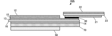
- FIG. 3 is a cross-sectional view of the pressing sensor 10A of the modified example 1.
- the same reference numerals are given to the configurations common to those in FIG. 2B, and the description thereof will be omitted.
- the pressing sensor 10A of the first modification is provided with a reinforcing member 70 between the connecting member 50 and the second ground electrode 14.
- the reinforcing member 70 is made of, for example, a SUS plate.
- the reinforcing member 70 is a joining member such as solder, and is joined to the second ground electrode 14 and the connecting member 50. As a result, the pressing sensor 10A of the first modification improves the shielding property and the mechanical strength of the joining member 30.
- FIG. 4A is a plan view of the pressing sensor 10B according to the modified example 2
- FIG. 4B is a cross-sectional view taken along the line AA.
- the same reference numerals are given to the configurations common to those in FIGS. 2 (A) and 2 (B), and the description thereof will be omitted.
- the electrodes formed on the first main surface and the second main surface of the base material 16 are patterned.
- the electrode formed on the first main surface is divided into a detection electrode 13A and a ground electrode 13B.
- the detection electrode 13A is arranged at a position facing the piezoelectric film 15.
- the ground electrode 13B is arranged at a position not facing the piezoelectric film 15 and at a position where the base material 16 and the wiring 20 overlap with each other in a substantially plan view.
- the electrode formed on the second main surface is divided into a detection electrode 14A and a ground electrode 14B.
- the detection electrode 14A is formed at a position where the base material 16 and the wiring 20 overlap each other and a position where the piezoelectric film 15 partially overlaps in a plan view.
- the detection electrode 14A is formed at a position excluding both ends of the base material 16 in the minor axis direction.
- the ground electrode 13B is formed at a position where the ground electrode 13B overlaps substantially the entire surface of the piezoelectric film 15 in a plan view and a position where the base material 16 and the wiring 20 overlap in a plan view.
- the ground electrodes 13B are arranged on both ends in the short axis direction at positions where the base material 16 and the wiring 20 overlap in a plan view.
- the detection electrode 13A and the detection electrode 14A are electrically connected by a via conductor 90 at a position where they overlap with the piezoelectric film 15 in a plan view.
- the position of the via conductor 90 is not limited to this example. That is, in this example, the detection electrodes include a first electrode (detection electrode 13A) arranged on the first surface side of the base material 16 and a second electrode (detection electrode 14A) arranged on the second surface side. Consists of.
- the electrodes formed on the first main surface of the wiring base material 23 are also patterned.
- the electrode formed on the first main surface of the wiring base material 23 is divided into a wiring detection electrode 21A and a wiring ground electrode 21B.
- the wiring detection electrode 21A is formed at a position excluding both ends of the wiring base material 23 in the minor axis direction in a plan view.
- the wiring ground electrode 21B is formed on both ends of the wiring base material 23 in the short axis direction in a plan view.
- the wiring detection electrode 21A and the detection electrode 14A are connected by a joining member 30. Further, the wiring ground electrode 21B and the ground electrode 14B are connected by another joining member (not shown).
- the first ground electrode 12A is attached to the upper surface of the piezoelectric film 15.
- the first ground electrode 12A is composed of, for example, a conductive pressure-sensitive adhesive and a metal thin film.
- the first ground electrode 12A is attached so as to cover not only the upper surface of the piezoelectric film 15 but also the entire surface of the base material 16.
- the first ground electrode 12A is also attached to the ground electrode 13B.
- the ground electrode 13B is connected to the ground electrode 14B by a via conductor (not shown) or the like. That is, in this example, the first ground electrode is composed of the first ground electrode 12A of the conductive member attached to the piezoelectric film 15 and the ground electrode 13B arranged on the first surface side of the base material 16. ..
- the pressing sensor 10B of the second modification joins the wiring 20 on the second main surface side of the base material 16 opposite to the first main surface side on which the piezoelectric film 15 is arranged. As a result, it is not necessary to provide a mounting portion for connecting the wiring 20 on the first main surface side where the piezoelectric film 15 is arranged. That is, the pressing sensor 10B of the modification 2 can increase the occupied area of the piezoelectric film 15. In other words, even if the area of the same piezoelectric film 15 is the same, the area of the sensor as a whole can be reduced.
- FIG. 5 is a cross-sectional view of the pressing sensor 10C according to the modified example 3.
- the same reference numerals are given to the configurations common to the cross-sectional view of FIG. 4B, and the description thereof will be omitted.
- the area of the piezoelectric film 15 is larger than that of the pressing sensor 10B of the modified example 2.
- the piezoelectric film 15 is also arranged at a position where it overlaps with the joining member 30 in a plan view. As a result, the pressing sensor 10C of the modified example 3 can further increase the occupied area of the piezoelectric film 15.
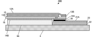
- FIG. 6 is a cross-sectional view of the pressing sensor 10D according to the modified example 4.
- the same reference numerals are given to the configurations common to the cross-sectional view of FIG. 5, and the description thereof will be omitted.
- the wiring 20 is connected to the surface panel 3 which is the object of deformation detection.
- the wiring ground electrode 22 of the wiring 20 is in contact with the surface panel 3, but in reality, the wiring 20 is attached to and fixed to the surface panel 3 via an adhesive or the like.
- the surface panel 3 is the object of deformation detection, but of course, the housing 2 may be the object of deformation detection.
- the pressing sensor 10D connects the wiring 20 to the object for deformation detection, when the object is deformed, the strain due to the deformation of the object is transmitted to the piezoelectric film 15 via the connecting portion of the wiring 20. can do. As a result, the detection sensitivity of the pressing sensor 10D is improved. For example, when the output of the pressing sensor 10C in FIG. 5 is 0.15Vpp (Vpp is a peak to peak voltage), the output of the pressing sensor 10D in FIG. 6 under the same conditions is 0.22Vpp, which is about 0.22Vpp. It improves by 1.5 times. In addition, strain can be detected in a portion having an area larger than the area of the piezoelectric film 15. In particular, the detection sensitivity of pressing against the connection portion with the wiring 20 is remarkably improved.
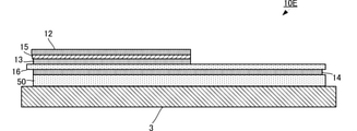
- FIG. 7 is a cross-sectional view of the pressing sensor 10E according to the modified example 5.
- the same reference numerals are given to the configurations common to the cross-sectional view of FIG. 2B, and the description thereof will be omitted.
- the base material 16 and the connecting member 50 are laterally extended along the long axis direction of the piezoelectric film 15 in a plan view.
- the second ground electrode 14 is also laterally extended along the long axis direction of the piezoelectric film 15 in a plan view, but it is not essential that the second ground electrode 14 is laterally extended. ..
- the base material 16 and the connecting member 50 are connected to the surface panel 3 which is the object of deformation detection. That is, the base material 16 is connected to the object for deformation detection even at a position where the piezoelectric film 15 is not arranged in a plan view. Therefore, when the object is deformed, the strain due to the deformation of the object can be transmitted to the piezoelectric film 15 via the connecting portion. As a result, the detection sensitivity of the pressing sensor 10E is improved. In addition, strain can be detected in a portion having an area larger than the area of the piezoelectric film 15. In particular, the detection sensitivity of pressing on the laterally extended portion is significantly improved.
- FIG. 8 is a plan view showing the overall structure of the pressing sensor 10F
- FIG. 9A is a perspective view of the pressing sensor 10F
- FIG. 9B is a partially exploded perspective view.
- 10 (A) is a cross-sectional view taken along the line AA shown in FIG. 10
- (B) is a cross-sectional view taken along the line BB shown in FIG.
- the pressing sensor 10F of this example has a sensor unit 80 and a wiring unit 81.
- the wiring unit 81 has a circuit component 39 such as an amplifier circuit and an output terminal 390.
- the sensor unit 80 has an adhesive 200 and a separator 201.
- the pressure-sensitive adhesive 200 is attached to the ground electrode 14B.
- the pressure-sensitive adhesive 200 is composed of, for example, an acrylic pressure-sensitive adhesive.
- a separator 201 is attached to the pressure-sensitive adhesive 200.
- the separator 201 protects the adhesive surface of the adhesive 200.
- the separator 201 has a mold release portion for peeling off the separator 201.
- the release portion is a portion of the separator 201 that is not attached to the pressure-sensitive adhesive 200.
- a user of the piezoelectric sensor 100 peels off the separator 201 by picking and pulling the release portion with tweezers or the like.
- the adhesive 200 after peeling off the separator 201 is attached to a housing or the like of an electronic component.
- the circuit component 39 does not necessarily have to be provided.
- the first ground electrode 12A is attached to the ground electrode 13B. However, in this example, the first ground electrode 12A does not overlap the joining member 30 in a plan view. If both the first ground electrode 12A and the ground electrode 13B overlap the joining member 30, and the thickness of the first ground electrode 12A varies, the bonding strength of the bonding member 30 may vary. be. Further, if both the first ground electrode 12A and the ground electrode 13B overlap the joining member 30 and the first ground electrode 12A is deformed by heat, the adhesion between the first ground electrode 12A and the ground electrode 13B varies. It may occur. In this case, the stress related to the piezoelectric film 15 may vary, and the characteristics of the sensor may vary. However, since the first ground electrode 12A does not overlap the joining member 30 in a plan view, it is possible to prevent such variations in joining strength and adhesion.
- the ground electrode 13B overlaps the base material 16 and the joining member 30 in a plan view. Since the ground electrode 13B overlaps the base material 16, the main surface of the base material 16 can be easily held in a flat shape. If the ground electrode 13B is also configured so as not to overlap the joining member 30 in a plan view, the main surface of the base material 16 may not be flat due to the influence of the shape of the wiring detection electrode 21A, and the joining strength of the joining member 30 varies. May occur. In the present embodiment, since the ground electrode 13B overlaps the base material 16, the main surface of the base material 16 is maintained in a flat shape, and it is possible to prevent variations in the joining strength of the joining member 30.
- the length (width) A1 of the joining member 30 along the X direction is wider than the width A2 of the detection electrode 14A and the width A3 of the wiring detection electrode 21A. ..
- the width A3 of the wiring detection electrode 21A is wider than the width A2 of the detection electrode 14A.
- the width A2 of the detection electrode 14A may be wider than the width A3 of the wiring detection electrode 21A.
- one of the width A3 of the wiring detection electrode 21A and the width A2 of the detection electrode 14A is wider than the other.
- the entire main surface of either the wiring detection electrode 21A or the detection electrode 14A overlaps with the other main surface. Therefore, the stability when the joining member 30 is thermocompression bonded and joined is improved.
- the width A4 of the ground electrode 13B and the width A4 of the wiring ground electrode 22 are wider than the width A2 of the detection electrode 14A and the width A3 of the wiring detection electrode 21A.
- the ground electrodes such as the ground electrode 13B and the wiring ground electrode 22 reinforce the joint portion. Since the width of the ground electrode is wider than the width of the detection electrode, the stability when the joining member 30 is thermocompression bonded and joined is further improved, and it is possible to prevent the occurrence of high thermal stress or the like locally.
- the ground electrode is a solid electrode that is not patterned at the joint portion.
- the wiring portion 81 has a portion (constricted portion 85) whose width is shortened in a plan view.
- the wiring portion 81 has a constricted portion 85, so that the flexibility is improved.
- the wiring portion 81 can relieve the stress by the constricted portion 85 and suppress the stress from being transmitted to the sensor portion 80, and the sensor can be suppressed. It is possible to prevent malfunction.
- both main surfaces of the sensor unit 80 and the wiring unit 81 are covered with a resist (not shown), the resist (not shown) may be removed around the constricted portion 85.
- the wiring portion 81 can further improve the flexibility by removing the resist around the constricted portion 85.
Landscapes
- Engineering & Computer Science (AREA)
- Manufacturing & Machinery (AREA)
- Physics & Mathematics (AREA)
- General Physics & Mathematics (AREA)
- Measurement Of Length, Angles, Or The Like Using Electric Or Magnetic Means (AREA)
- Force Measurement Appropriate To Specific Purposes (AREA)
Abstract
Description
2…筐体
3…表面パネル
4…表示装置
5…静電容量センサ
6…表示部
10,10A,10B,10C…押圧センサ
12,12A…第1グランド電極
13,13A…検出電極
13B…グランド電極
14…第2グランド電極
14A…検出電極
14B…グランド電極
15…圧電フィルム
16…基材
20…配線
21,21A…配線検出電極
22…配線グランド電極
21B…配線グランド電極
23…配線基材
30…接合部材
50…接続部材
70…補強部材
90…ビア導体
Claims (6)
- 検出電極と、
第1グランド電極と、
第2グランド電極と、
前記検出電極および前記第1グランド電極で挟まれる圧電フィルムと、
前記検出電極および前記第2グランド電極が形成された基材と、
前記検出電極に接続される配線と、
前記配線および前記検出電極を接合する接合部材と、
を備え、
前記接合部材は、前記基材のうち前記圧電フィルムが配置される第1面側と反対側の第2面側に配置される、
変形検出センサ。 - 前記基材を補強し、前記第2グランド電極に接続され、前記基材を補強する補強部材を備えた、
請求項1に記載の変形検出センサ。 - 前記検出電極は、前記基材のうち前記第1面側に配置される第1電極と、前記第2面側に配置される第2電極と、からなり、
前記第1電極と前記第2電極とを電気的に接続するビア導体を備える、
請求項1または請求項2に記載の変形検出センサ。 - 前記第1グランド電極は、前記圧電フィルムに貼り付けられる導電性部材と、前記基材のうち前記第1面側に配置される第1電極と、からなる、
請求項1乃至請求項3のいずれか1項に記載の変形検出センサ。 - 前記配線は、変形検出の対象物に接続される、
請求項1乃至請求項4のいずれか1項に記載の変形検出センサ。 - 前記接合部材は平面視して前記第1グランド電極と重なる、請求項1乃至請求項5のいずれか1項に記載の変形検出センサ。
Priority Applications (4)
| Application Number | Priority Date | Filing Date | Title |
|---|---|---|---|
| CN202180010660.6A CN114981614B (zh) | 2020-07-30 | 2021-07-30 | 变形检测传感器 |
| JP2022521465A JP7088442B1 (ja) | 2020-07-30 | 2021-07-30 | 変形検出センサ |
| JP2022088492A JP7416128B2 (ja) | 2020-07-30 | 2022-05-31 | 変形検出センサ |
| US17/864,019 US12484448B2 (en) | 2020-07-30 | 2022-07-13 | Deformation detection sensor |
Applications Claiming Priority (2)
| Application Number | Priority Date | Filing Date | Title |
|---|---|---|---|
| JP2020-129282 | 2020-07-30 | ||
| JP2020129282 | 2020-07-30 |
Related Child Applications (1)
| Application Number | Title | Priority Date | Filing Date |
|---|---|---|---|
| US17/864,019 Continuation US12484448B2 (en) | 2020-07-30 | 2022-07-13 | Deformation detection sensor |
Publications (1)
| Publication Number | Publication Date |
|---|---|
| WO2022025232A1 true WO2022025232A1 (ja) | 2022-02-03 |
Family
ID=80035805
Family Applications (1)
| Application Number | Title | Priority Date | Filing Date |
|---|---|---|---|
| PCT/JP2021/028283 Ceased WO2022025232A1 (ja) | 2020-07-30 | 2021-07-30 | 変形検出センサ |
Country Status (4)
| Country | Link |
|---|---|
| US (1) | US12484448B2 (ja) |
| JP (2) | JP7088442B1 (ja) |
| CN (1) | CN114981614B (ja) |
| WO (1) | WO2022025232A1 (ja) |
Citations (5)
| Publication number | Priority date | Publication date | Assignee | Title |
|---|---|---|---|---|
| JP2004118754A (ja) * | 2002-09-30 | 2004-04-15 | Smk Corp | タッチパネル |
| JP2013178241A (ja) * | 2012-02-07 | 2013-09-09 | Sumitomo Electric Ind Ltd | 圧力感知センサ搭載配線板 |
| JP2015018368A (ja) * | 2013-07-10 | 2015-01-29 | 住友電気工業株式会社 | 感圧式タッチ入力部材付き表示装置 |
| WO2015159628A1 (ja) * | 2014-04-18 | 2015-10-22 | 株式会社村田製作所 | 押圧センサ |
| WO2019021981A1 (ja) * | 2017-07-26 | 2019-01-31 | 株式会社村田製作所 | 押圧センサ及び電子機器 |
Family Cites Families (14)
| Publication number | Priority date | Publication date | Assignee | Title |
|---|---|---|---|---|
| US4555953A (en) * | 1984-04-16 | 1985-12-03 | Paolo Dario | Composite, multifunctional tactile sensor |
| JP4946763B2 (ja) * | 2007-10-01 | 2012-06-06 | ブラザー工業株式会社 | 屈曲検出装置 |
| JP5526761B2 (ja) * | 2009-12-22 | 2014-06-18 | ソニー株式会社 | センサ装置及び情報処理装置 |
| JP5216041B2 (ja) * | 2010-04-07 | 2013-06-19 | ダイキン工業株式会社 | 透明圧電シートをそれぞれ有するフレーム付透明圧電シート、タッチパネル、および電子装置 |
| US8985734B2 (en) * | 2012-08-31 | 2015-03-24 | Brother Kogyo Kabushiki Kaisha | Liquid jetting apparatus, piezoelectric actuator, and method for producing the liquid jetting apparatus |
| JP6294177B2 (ja) * | 2013-07-10 | 2018-03-14 | 積水化学工業株式会社 | 圧電センサ |
| US20160274724A1 (en) * | 2015-03-20 | 2016-09-22 | Egalax_Empia Technology Inc. | Pressure Sensing and Touch Sensitive Panel, Pressure Sensing Method, Pressure Sensing Electronic Device and Control Unit Thereof |
| WO2016194690A1 (ja) * | 2015-05-29 | 2016-12-08 | 株式会社村田製作所 | 圧電フィルムセンサおよび保持状態検出装置 |
| JP6447779B2 (ja) * | 2016-04-22 | 2019-01-09 | 株式会社村田製作所 | モニタリングシステム |
| WO2017208798A1 (ja) * | 2016-05-30 | 2017-12-07 | 株式会社村田製作所 | 表示装置及び表示システム |
| JP6489290B2 (ja) * | 2016-08-03 | 2019-03-27 | 株式会社村田製作所 | 変形検知センサ、電子機器、および変形検知センサの製造方法 |
| KR102638861B1 (ko) * | 2016-09-06 | 2024-02-22 | 세키스이가가쿠 고교가부시키가이샤 | 압전 센서 |
| KR102249961B1 (ko) * | 2017-08-08 | 2021-05-11 | 알프스 알파인 가부시키가이샤 | 입력 장치의 제조 방법 및 입력 장치 |
| CN213120923U (zh) * | 2018-12-20 | 2021-05-04 | 株式会社村田制作所 | 按压传感器和按压检测装置 |
-
2021
- 2021-07-30 WO PCT/JP2021/028283 patent/WO2022025232A1/ja not_active Ceased
- 2021-07-30 CN CN202180010660.6A patent/CN114981614B/zh active Active
- 2021-07-30 JP JP2022521465A patent/JP7088442B1/ja active Active
-
2022
- 2022-05-31 JP JP2022088492A patent/JP7416128B2/ja active Active
- 2022-07-13 US US17/864,019 patent/US12484448B2/en active Active
Patent Citations (5)
| Publication number | Priority date | Publication date | Assignee | Title |
|---|---|---|---|---|
| JP2004118754A (ja) * | 2002-09-30 | 2004-04-15 | Smk Corp | タッチパネル |
| JP2013178241A (ja) * | 2012-02-07 | 2013-09-09 | Sumitomo Electric Ind Ltd | 圧力感知センサ搭載配線板 |
| JP2015018368A (ja) * | 2013-07-10 | 2015-01-29 | 住友電気工業株式会社 | 感圧式タッチ入力部材付き表示装置 |
| WO2015159628A1 (ja) * | 2014-04-18 | 2015-10-22 | 株式会社村田製作所 | 押圧センサ |
| WO2019021981A1 (ja) * | 2017-07-26 | 2019-01-31 | 株式会社村田製作所 | 押圧センサ及び電子機器 |
Also Published As
| Publication number | Publication date |
|---|---|
| JPWO2022025232A1 (ja) | 2022-02-03 |
| CN114981614A (zh) | 2022-08-30 |
| JP2022125027A (ja) | 2022-08-26 |
| JP7088442B1 (ja) | 2022-06-21 |
| US20220344572A1 (en) | 2022-10-27 |
| US12484448B2 (en) | 2025-11-25 |
| JP7416128B2 (ja) | 2024-01-17 |
| CN114981614B (zh) | 2025-09-16 |
Similar Documents
| Publication | Publication Date | Title |
|---|---|---|
| JP5605433B2 (ja) | 圧電振動装置 | |
| US11733109B2 (en) | Force sensor and manufacturing method thereof | |
| CN110352337B (zh) | 应变体及具备该应变体的力传感器 | |
| TWI644083B (zh) | 超聲波感測器及具有該超聲波感測器之電子裝置 | |
| CN102483363B (zh) | 压力检测单元以及压力检测装置 | |
| CN108235748B (zh) | 压阻式传感器、压力检测装置、电子设备 | |
| CN108291796B (zh) | 压电挠曲传感器以及检测装置 | |
| CN110325832A (zh) | 应变体及具备该应变体的力传感器 | |
| CN114981761B (zh) | 触觉效果装置 | |
| JP6776151B2 (ja) | 起歪体およびその起歪体を備えた力覚センサ | |
| JP7088442B1 (ja) | 変形検出センサ | |
| WO2022006844A1 (zh) | 触觉反馈单元、触觉反馈装置和电子设备 | |
| CN215494958U (zh) | 压力感应模组及触控装置 | |
| US10541359B2 (en) | Simple-assembly sensing device | |
| CN212659039U (zh) | 触觉反馈装置和电子设备 | |
| JP6022967B2 (ja) | 振動装置、電子機器、および携帯端末 | |
| WO2025118257A1 (zh) | 压电换能器及压力感应按键 | |
| JP2018092223A (ja) | 指紋検出装置、電子装置 | |
| CN111813225A (zh) | 触觉反馈单元、触觉反馈装置和电子设备 | |
| CN221978921U (zh) | 感应模组、按键组件及电子设备 | |
| CN105760001A (zh) | 触控装置以及采用该触控装置的电子设备 | |
| CN115016662B (zh) | 电子装置 | |
| CN212659040U (zh) | 触觉反馈单元、触觉反馈装置和电子设备 | |
| CN115996621A (zh) | 按压传感器 | |
| JP2007052974A (ja) | 静電容量式スイッチ装置 |
Legal Events
| Date | Code | Title | Description |
|---|---|---|---|
| 121 | Ep: the epo has been informed by wipo that ep was designated in this application |
Ref document number: 21849761 Country of ref document: EP Kind code of ref document: A1 |
|
| ENP | Entry into the national phase |
Ref document number: 2022521465 Country of ref document: JP Kind code of ref document: A |
|
| NENP | Non-entry into the national phase |
Ref country code: DE |
|
| 122 | Ep: pct application non-entry in european phase |
Ref document number: 21849761 Country of ref document: EP Kind code of ref document: A1 |
|
| WWG | Wipo information: grant in national office |
Ref document number: 202180010660.6 Country of ref document: CN |