WO2022024813A1 - SiC半導体装置 - Google Patents
SiC半導体装置 Download PDFInfo
- Publication number
- WO2022024813A1 WO2022024813A1 PCT/JP2021/026791 JP2021026791W WO2022024813A1 WO 2022024813 A1 WO2022024813 A1 WO 2022024813A1 JP 2021026791 W JP2021026791 W JP 2021026791W WO 2022024813 A1 WO2022024813 A1 WO 2022024813A1
- Authority
- WO
- WIPO (PCT)
- Prior art keywords
- trench
- source
- gate
- insulating film
- electrode
- Prior art date
- Legal status (The legal status is an assumption and is not a legal conclusion. Google has not performed a legal analysis and makes no representation as to the accuracy of the status listed.)
- Ceased
Links
Images

















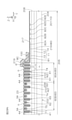
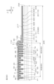


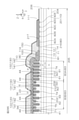
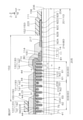




Classifications
-
- H—ELECTRICITY
- H10—SEMICONDUCTOR DEVICES; ELECTRIC SOLID-STATE DEVICES NOT OTHERWISE PROVIDED FOR
- H10D—INORGANIC ELECTRIC SEMICONDUCTOR DEVICES
- H10D62/00—Semiconductor bodies, or regions thereof, of devices having potential barriers
- H10D62/10—Shapes, relative sizes or dispositions of the regions of the semiconductor bodies; Shapes of the semiconductor bodies
- H10D62/13—Semiconductor regions connected to electrodes carrying current to be rectified, amplified or switched, e.g. source or drain regions
- H10D62/149—Source or drain regions of field-effect devices
- H10D62/151—Source or drain regions of field-effect devices of IGFETs
- H10D62/152—Source regions of DMOS transistors
- H10D62/155—Shapes
-
- H—ELECTRICITY
- H10—SEMICONDUCTOR DEVICES; ELECTRIC SOLID-STATE DEVICES NOT OTHERWISE PROVIDED FOR
- H10D—INORGANIC ELECTRIC SEMICONDUCTOR DEVICES
- H10D62/00—Semiconductor bodies, or regions thereof, of devices having potential barriers
- H10D62/80—Semiconductor bodies, or regions thereof, of devices having potential barriers characterised by the materials
- H10D62/83—Semiconductor bodies, or regions thereof, of devices having potential barriers characterised by the materials being Group IV materials, e.g. B-doped Si or undoped Ge
- H10D62/832—Semiconductor bodies, or regions thereof, of devices having potential barriers characterised by the materials being Group IV materials, e.g. B-doped Si or undoped Ge being Group IV materials comprising two or more elements, e.g. SiGe
- H10D62/8325—Silicon carbide
-
- H—ELECTRICITY
- H10—SEMICONDUCTOR DEVICES; ELECTRIC SOLID-STATE DEVICES NOT OTHERWISE PROVIDED FOR
- H10D—INORGANIC ELECTRIC SEMICONDUCTOR DEVICES
- H10D12/00—Bipolar devices controlled by the field effect, e.g. insulated-gate bipolar transistors [IGBT]
- H10D12/01—Manufacture or treatment
- H10D12/031—Manufacture or treatment of IGBTs
-
- H—ELECTRICITY
- H10—SEMICONDUCTOR DEVICES; ELECTRIC SOLID-STATE DEVICES NOT OTHERWISE PROVIDED FOR
- H10D—INORGANIC ELECTRIC SEMICONDUCTOR DEVICES
- H10D30/00—Field-effect transistors [FET]
- H10D30/01—Manufacture or treatment
- H10D30/021—Manufacture or treatment of FETs having insulated gates [IGFET]
- H10D30/028—Manufacture or treatment of FETs having insulated gates [IGFET] of double-diffused metal oxide semiconductor [DMOS] FETs
- H10D30/0291—Manufacture or treatment of FETs having insulated gates [IGFET] of double-diffused metal oxide semiconductor [DMOS] FETs of vertical DMOS [VDMOS] FETs
- H10D30/0295—Manufacture or treatment of FETs having insulated gates [IGFET] of double-diffused metal oxide semiconductor [DMOS] FETs of vertical DMOS [VDMOS] FETs using recessing of the source electrodes
-
- H—ELECTRICITY
- H10—SEMICONDUCTOR DEVICES; ELECTRIC SOLID-STATE DEVICES NOT OTHERWISE PROVIDED FOR
- H10D—INORGANIC ELECTRIC SEMICONDUCTOR DEVICES
- H10D30/00—Field-effect transistors [FET]
- H10D30/01—Manufacture or treatment
- H10D30/021—Manufacture or treatment of FETs having insulated gates [IGFET]
- H10D30/028—Manufacture or treatment of FETs having insulated gates [IGFET] of double-diffused metal oxide semiconductor [DMOS] FETs
- H10D30/0291—Manufacture or treatment of FETs having insulated gates [IGFET] of double-diffused metal oxide semiconductor [DMOS] FETs of vertical DMOS [VDMOS] FETs
- H10D30/0297—Manufacture or treatment of FETs having insulated gates [IGFET] of double-diffused metal oxide semiconductor [DMOS] FETs of vertical DMOS [VDMOS] FETs using recessing of the gate electrodes, e.g. to form trench gate electrodes
-
- H—ELECTRICITY
- H10—SEMICONDUCTOR DEVICES; ELECTRIC SOLID-STATE DEVICES NOT OTHERWISE PROVIDED FOR
- H10D—INORGANIC ELECTRIC SEMICONDUCTOR DEVICES
- H10D30/00—Field-effect transistors [FET]
- H10D30/60—Insulated-gate field-effect transistors [IGFET]
- H10D30/64—Double-diffused metal-oxide semiconductor [DMOS] FETs
- H10D30/66—Vertical DMOS [VDMOS] FETs
- H10D30/665—Vertical DMOS [VDMOS] FETs having edge termination structures
-
- H—ELECTRICITY
- H10—SEMICONDUCTOR DEVICES; ELECTRIC SOLID-STATE DEVICES NOT OTHERWISE PROVIDED FOR
- H10D—INORGANIC ELECTRIC SEMICONDUCTOR DEVICES
- H10D30/00—Field-effect transistors [FET]
- H10D30/60—Insulated-gate field-effect transistors [IGFET]
- H10D30/64—Double-diffused metal-oxide semiconductor [DMOS] FETs
- H10D30/66—Vertical DMOS [VDMOS] FETs
- H10D30/668—Vertical DMOS [VDMOS] FETs having trench gate electrodes, e.g. UMOS transistors
-
- H—ELECTRICITY
- H10—SEMICONDUCTOR DEVICES; ELECTRIC SOLID-STATE DEVICES NOT OTHERWISE PROVIDED FOR
- H10D—INORGANIC ELECTRIC SEMICONDUCTOR DEVICES
- H10D62/00—Semiconductor bodies, or regions thereof, of devices having potential barriers
- H10D62/10—Shapes, relative sizes or dispositions of the regions of the semiconductor bodies; Shapes of the semiconductor bodies
- H10D62/102—Constructional design considerations for preventing surface leakage or controlling electric field concentration
- H10D62/103—Constructional design considerations for preventing surface leakage or controlling electric field concentration for increasing or controlling the breakdown voltage of reverse-biased devices
- H10D62/104—Constructional design considerations for preventing surface leakage or controlling electric field concentration for increasing or controlling the breakdown voltage of reverse-biased devices having particular shapes of the bodies at or near reverse-biased junctions, e.g. having bevels or moats
-
- H—ELECTRICITY
- H10—SEMICONDUCTOR DEVICES; ELECTRIC SOLID-STATE DEVICES NOT OTHERWISE PROVIDED FOR
- H10D—INORGANIC ELECTRIC SEMICONDUCTOR DEVICES
- H10D62/00—Semiconductor bodies, or regions thereof, of devices having potential barriers
- H10D62/10—Shapes, relative sizes or dispositions of the regions of the semiconductor bodies; Shapes of the semiconductor bodies
- H10D62/102—Constructional design considerations for preventing surface leakage or controlling electric field concentration
- H10D62/103—Constructional design considerations for preventing surface leakage or controlling electric field concentration for increasing or controlling the breakdown voltage of reverse-biased devices
- H10D62/105—Constructional design considerations for preventing surface leakage or controlling electric field concentration for increasing or controlling the breakdown voltage of reverse-biased devices by having particular doping profiles, shapes or arrangements of PN junctions; by having supplementary regions, e.g. junction termination extension [JTE]
-
- H—ELECTRICITY
- H10—SEMICONDUCTOR DEVICES; ELECTRIC SOLID-STATE DEVICES NOT OTHERWISE PROVIDED FOR
- H10D—INORGANIC ELECTRIC SEMICONDUCTOR DEVICES
- H10D62/00—Semiconductor bodies, or regions thereof, of devices having potential barriers
- H10D62/10—Shapes, relative sizes or dispositions of the regions of the semiconductor bodies; Shapes of the semiconductor bodies
- H10D62/102—Constructional design considerations for preventing surface leakage or controlling electric field concentration
- H10D62/103—Constructional design considerations for preventing surface leakage or controlling electric field concentration for increasing or controlling the breakdown voltage of reverse-biased devices
- H10D62/105—Constructional design considerations for preventing surface leakage or controlling electric field concentration for increasing or controlling the breakdown voltage of reverse-biased devices by having particular doping profiles, shapes or arrangements of PN junctions; by having supplementary regions, e.g. junction termination extension [JTE]
- H10D62/106—Constructional design considerations for preventing surface leakage or controlling electric field concentration for increasing or controlling the breakdown voltage of reverse-biased devices by having particular doping profiles, shapes or arrangements of PN junctions; by having supplementary regions, e.g. junction termination extension [JTE] having supplementary regions doped oppositely to or in rectifying contact with regions of the semiconductor bodies, e.g. guard rings with PN or Schottky junctions
-
- H—ELECTRICITY
- H10—SEMICONDUCTOR DEVICES; ELECTRIC SOLID-STATE DEVICES NOT OTHERWISE PROVIDED FOR
- H10D—INORGANIC ELECTRIC SEMICONDUCTOR DEVICES
- H10D62/00—Semiconductor bodies, or regions thereof, of devices having potential barriers
- H10D62/10—Shapes, relative sizes or dispositions of the regions of the semiconductor bodies; Shapes of the semiconductor bodies
- H10D62/102—Constructional design considerations for preventing surface leakage or controlling electric field concentration
- H10D62/103—Constructional design considerations for preventing surface leakage or controlling electric field concentration for increasing or controlling the breakdown voltage of reverse-biased devices
- H10D62/105—Constructional design considerations for preventing surface leakage or controlling electric field concentration for increasing or controlling the breakdown voltage of reverse-biased devices by having particular doping profiles, shapes or arrangements of PN junctions; by having supplementary regions, e.g. junction termination extension [JTE]
- H10D62/109—Reduced surface field [RESURF] PN junction structures
-
- H—ELECTRICITY
- H10—SEMICONDUCTOR DEVICES; ELECTRIC SOLID-STATE DEVICES NOT OTHERWISE PROVIDED FOR
- H10D—INORGANIC ELECTRIC SEMICONDUCTOR DEVICES
- H10D62/00—Semiconductor bodies, or regions thereof, of devices having potential barriers
- H10D62/10—Shapes, relative sizes or dispositions of the regions of the semiconductor bodies; Shapes of the semiconductor bodies
- H10D62/124—Shapes, relative sizes or dispositions of the regions of semiconductor bodies or of junctions between the regions
- H10D62/126—Top-view geometrical layouts of the regions or the junctions
- H10D62/127—Top-view geometrical layouts of the regions or the junctions of cellular field-effect devices, e.g. multicellular DMOS transistors or IGBTs
-
- H—ELECTRICITY
- H10—SEMICONDUCTOR DEVICES; ELECTRIC SOLID-STATE DEVICES NOT OTHERWISE PROVIDED FOR
- H10D—INORGANIC ELECTRIC SEMICONDUCTOR DEVICES
- H10D62/00—Semiconductor bodies, or regions thereof, of devices having potential barriers
- H10D62/10—Shapes, relative sizes or dispositions of the regions of the semiconductor bodies; Shapes of the semiconductor bodies
- H10D62/13—Semiconductor regions connected to electrodes carrying current to be rectified, amplified or switched, e.g. source or drain regions
- H10D62/149—Source or drain regions of field-effect devices
- H10D62/151—Source or drain regions of field-effect devices of IGFETs
- H10D62/156—Drain regions of DMOS transistors
- H10D62/157—Impurity concentrations or distributions
-
- H—ELECTRICITY
- H10—SEMICONDUCTOR DEVICES; ELECTRIC SOLID-STATE DEVICES NOT OTHERWISE PROVIDED FOR
- H10D—INORGANIC ELECTRIC SEMICONDUCTOR DEVICES
- H10D64/00—Electrodes of devices having potential barriers
- H10D64/111—Field plates
- H10D64/117—Recessed field plates, e.g. trench field plates or buried field plates
-
- H—ELECTRICITY
- H10—SEMICONDUCTOR DEVICES; ELECTRIC SOLID-STATE DEVICES NOT OTHERWISE PROVIDED FOR
- H10D—INORGANIC ELECTRIC SEMICONDUCTOR DEVICES
- H10D64/00—Electrodes of devices having potential barriers
- H10D64/20—Electrodes characterised by their shapes, relative sizes or dispositions
- H10D64/23—Electrodes carrying the current to be rectified, amplified, oscillated or switched, e.g. sources, drains, anodes or cathodes
- H10D64/251—Source or drain electrodes for field-effect devices
- H10D64/252—Source or drain electrodes for field-effect devices for vertical or pseudo-vertical devices
-
- H—ELECTRICITY
- H10—SEMICONDUCTOR DEVICES; ELECTRIC SOLID-STATE DEVICES NOT OTHERWISE PROVIDED FOR
- H10D—INORGANIC ELECTRIC SEMICONDUCTOR DEVICES
- H10D64/00—Electrodes of devices having potential barriers
- H10D64/20—Electrodes characterised by their shapes, relative sizes or dispositions
- H10D64/23—Electrodes carrying the current to be rectified, amplified, oscillated or switched, e.g. sources, drains, anodes or cathodes
- H10D64/251—Source or drain electrodes for field-effect devices
- H10D64/252—Source or drain electrodes for field-effect devices for vertical or pseudo-vertical devices
- H10D64/2527—Source or drain electrodes for field-effect devices for vertical or pseudo-vertical devices for vertical devices wherein the source or drain electrodes are recessed in semiconductor bodies
-
- H—ELECTRICITY
- H10—SEMICONDUCTOR DEVICES; ELECTRIC SOLID-STATE DEVICES NOT OTHERWISE PROVIDED FOR
- H10D—INORGANIC ELECTRIC SEMICONDUCTOR DEVICES
- H10D64/00—Electrodes of devices having potential barriers
- H10D64/20—Electrodes characterised by their shapes, relative sizes or dispositions
- H10D64/27—Electrodes not carrying the current to be rectified, amplified, oscillated or switched, e.g. gates
- H10D64/311—Gate electrodes for field-effect devices
- H10D64/411—Gate electrodes for field-effect devices for FETs
- H10D64/511—Gate electrodes for field-effect devices for FETs for IGFETs
- H10D64/514—Gate electrodes for field-effect devices for FETs for IGFETs characterised by the insulating layers
- H10D64/516—Gate electrodes for field-effect devices for FETs for IGFETs characterised by the insulating layers the thicknesses being non-uniform
Definitions
- the present invention relates to a SiC semiconductor device.
- Patent Document 1 discloses a semiconductor device having a semiconductor substrate, a trench gate structure formed on the semiconductor substrate, and a trench source structure formed on the semiconductor substrate so as to be adjacent to the trench gate structure.
- One embodiment of the present invention provides a SiC semiconductor device capable of improving reliability.
- One embodiment of the present invention includes a SiC chip having a main surface, a trench gate structure formed on the main surface, and a trench source structure formed on the main surface separated from the trench gate structure in one direction.
- An insulating film that covers the trench gate structure and the trench source structure on the main surface, a gate main surface electrode formed on the insulating film, and the trench gate structure and the trench source in one direction. It is drawn from the gate main surface electrode so as to cross the structure onto the insulating film, penetrates the insulating film, is electrically connected to the trench gate structure, and faces the trench source structure with the insulating film interposed therebetween.
- a SiC semiconductor device including a gate wiring to be used.
- a SiC chip having a main surface, a trench gate structure formed on the main surface and extending in one direction in a plan view, and the main surface separated from the trench gate structure in one direction.
- An intermediate trench source structure formed on a surface and extending in one direction in a plan view, an insulating film covering the trench gate structure and the intermediate trench source structure, and an insulating film formed on the insulating film and penetrating the insulating film.
- the gate wiring electrically connected to the trench gate structure and the insulating film formed at a distance from the gate wiring, penetrate the insulating film, and electrically connect to the intermediate trench source structure.
- a SiC semiconductor device including a connected source wiring.
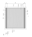
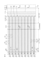
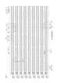
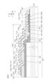
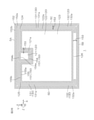
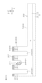
- FIG. 1 is a plan view showing a SiC semiconductor device according to the first embodiment of the present invention.
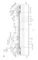
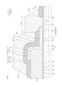
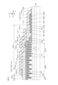
- FIG. 2 is a cross-sectional view showing a cross section along the line II-II shown in FIG. 1, omitting the structure inside the SiC chip.
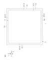
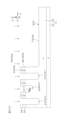
- FIG. 3 is a plan view showing the first main surface of the SiC chip shown in FIG. 1 by omitting the structure inside the SiC chip.
- FIG. 4 is a plan view showing a simplified structure in which the first main surface shown in FIG. 3 is built in the SiC chip.
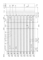
- FIG. 5 is an enlarged plan view of a main part of the first main surface shown in FIG.
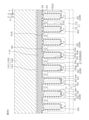
- FIG. 6 is an enlarged plan view of the end portion of the transistor region shown in FIG. FIG.
- FIG. 7 is an enlarged plan view of the inner portion of the transistor region shown in FIG.
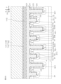
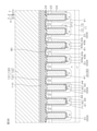
- FIG. 8 is a cross-sectional view taken along the line VIII-VIII shown in FIG.
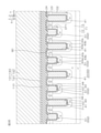
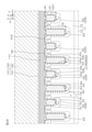
- FIG. 9 is a cross-sectional view taken along the line IX-IX shown in FIG.
- FIG. 10 is a cross-sectional view taken along the line XX shown in FIG.
- FIG. 11 is a cross-sectional view taken along the line XI-XI shown in FIG.
- FIG. 12 is a cross-sectional view taken along the line XII-XII shown in FIG.
- FIG. 13 is an enlarged plan view of a corner portion of the first peripheral edge region shown in FIG.
- FIG. 14 is a cross-sectional view taken along the line XIV-XIV shown in FIG.
- FIG. 15 is a cross-sectional view taken along the line XV-XV shown in FIG.
- FIG. 16 is an enlarged plan view of the end portion of the first peripheral edge region shown in FIG.
- FIG. 17 is an enlarged plan view of the inner portion of the first peripheral region shown in FIG.
- FIG. 18 is a cross-sectional view taken along the line XVIII-XVIII shown in FIG.
- FIG. 19 is a cross-sectional view taken along the line XIX-XIX shown in FIG.
- FIG. 20 is a cross-sectional view taken along the line XX-XX shown in FIG.
- FIG. 21 is a cross-sectional view taken along the line XXI-XXI shown in FIG. FIG.
- FIG. 22 is a cross-sectional view taken along the line XXII-XXII shown in FIG.
- FIG. 23 is a cross-sectional view taken along the line XXIII-XXIII shown in FIG.
- FIG. 24 is a cross-sectional view taken along the line XXIV-XXIV shown in FIG.
- FIG. 25 is a cross-sectional view taken along the line XXV-XXV shown in FIG.
- FIG. 26 is a cross-sectional view taken along the line XXVI-XXVI shown in FIG.
- FIG. 27 is a plan view for explaining the structure of the main surface electrode.
- FIG. 28 is a plan view for explaining the structure of the second inorganic insulating film.
- FIG. 29A is a cross-sectional view showing an example of a method for manufacturing the SiC semiconductor device shown in FIG.
- FIG. 29B is a cross-sectional view showing the process after FIG. 29A.
- FIG. 29C is a cross-sectional view showing the process after FIG. 29B.
- FIG. 29D is a cross-sectional view showing the process after FIG. 29C.
- FIG. 29E is a cross-sectional view showing the process after FIG. 29D.
- FIG. 29F is a cross-sectional view showing the process after FIG. 29E.
- FIG. 29G is a cross-sectional view showing the process after FIG. 29F.
- FIG. 29H is a cross-sectional view showing the process after FIG. 29G.
- FIG. 29A is a cross-sectional view showing an example of a method for manufacturing the SiC semiconductor device shown in FIG.
- FIG. 29B is a cross-sectional view showing the process after FIG. 29A.
- FIG. 29C is
- FIG. 29I is a cross-sectional view showing the process after FIG. 29H.
- FIG. 29J is a cross-sectional view showing the process after FIG. 29I.
- FIG. 29K is a cross-sectional view showing the process after FIG. 29J.
- FIG. 29L is a cross-sectional view showing the process after FIG. 29K.
- FIG. 29M is a cross-sectional view showing the process after FIG. 29L.
- FIG. 29N is a cross-sectional view showing the process after FIG. 29M.
- FIG. 29O is a cross-sectional view showing the process after FIG. 29N.
- FIG. 29P is a cross-sectional view showing the process after FIG. 29O.
- FIG. 29Q is a cross-sectional view showing the process after FIG. 29P.
- FIG. 29R is a cross-sectional view showing the process after FIG. 29Q.
- FIG. 29S is a cross-sectional view showing the process after FIG. 29R.
- FIG. 29T is a cross-sectional view showing the process after FIG. 29S.
- FIG. 29U is a cross-sectional view showing the process after FIG. 29T.
- FIG. 29V is a cross-sectional view showing the process after FIG. 29U.
- FIG. 30 is a plan view showing a SiC semiconductor device according to the first reference embodiment (first reference preferred embodiment) corresponding to FIG.
- FIG. 31A is a cross-sectional view showing an example of a method for manufacturing the SiC semiconductor device shown in FIG. 30.
- FIG. 31B is a cross-sectional view showing the process after FIG. 31A.
- FIG. 31C is a cross-sectional view showing the process after FIG. 31B.
- FIG. 31D is a cross-sectional view showing the process after FIG. 31C.
- FIG. 32 is a plan view showing a SiC semiconductor device according to a second reference embodiment (second reference preferred embodiment) corresponding to FIG.
- FIG. 33 is a cross-sectional view taken along the line XXXIII-XXXIII shown in FIG. 32.
- FIG. 34 is a plan view showing a SiC semiconductor device according to a second embodiment of the present invention, corresponding to FIG.
- FIG. 35 is a cross-sectional view taken along the line XXXV-XXXV shown in FIG. 34.
- FIG. 36 is a cross-sectional view taken along the line XXXVI-XXXVI shown in FIG. 34.
- FIG. 37 is a cross-sectional view taken along the line XXXVII-XXXVII shown in FIG. 34.
- FIG. 38 is a plan view showing the SiC semiconductor device shown in FIG. 34, which corresponds to FIG.
- FIG. 39 is a cross-sectional view taken along the line XXXIX-XXXIX shown in FIG. 38.
- FIG. 40 is a cross-sectional view taken along the line XL-XL shown in FIG. 38.
- FIG. 41 is a cross-sectional view taken along the line XLI-XLI shown in FIG. 38.
- FIG. 1 is a plan view showing a SiC semiconductor device 1 according to a first embodiment of the present invention.
- FIG. 2 is a cross-sectional view showing a cross section along the line II-II shown in FIG. 1, omitting the structure inside the SiC chip 2.
- FIG. 3 is a plan view showing the first main surface 3 of the SiC chip 2 shown in FIG. 1 by omitting the structure inside the SiC chip 2.
- the SiC semiconductor device 1 is an electronic component including a SiC chip 2 made of a hexagonal SiC (silicon carbide) single crystal in this embodiment. Further, the SiC semiconductor device 1 is a semiconductor switching device including a SiC-MISFET (Metal Insulator Semiconductor Field Effect Transistor) in this form.
- the hexagonal SiC single crystal has a plurality of polytypes including 2H (Hexagonal) -SiC single crystal, 4H-SiC single crystal, 6H-SiC single crystal and the like. In this embodiment, an example in which the SiC chip 2 is composed of a 4H-SiC single crystal is shown, but other polytypes are not excluded.
- the SiC chip 2 is formed in a rectangular parallelepiped shape.
- the SiC chip 2 has a first main surface 3 on one side, a second main surface 4 on the other side, and first to fourth side surfaces 5A to 5D connecting the first main surface 3 and the second main surface 4. is doing.
- the first main surface 3 is a device surface on which a functional device is formed.
- the second main surface 4 is a non-device surface on which a functional device is not formed.
- the first main surface 3 and the second main surface 4 are formed in a rectangular shape in a plan view (hereinafter, simply referred to as “plan view”) viewed from their normal direction Z.
- the first main surface 3 and the second main surface 4 may be formed in a square shape or a rectangular shape in a plan view.
- the first main surface 3 and the second main surface 4 face the c-plane of the SiC single crystal.
- the c-plane includes a silicon plane ((0001) plane) and a carbon plane ((000-1) plane) of the SiC single crystal. It is preferable that the first main surface 3 faces the silicon surface and the second main surface 4 faces the carbon surface.
- the first main surface 3 and the second main surface 4 may have an off angle inclined at a predetermined angle in a predetermined off direction with respect to the c surface.
- the off direction is preferably the a-axis direction ([11-20] direction) of the SiC single crystal.
- the off angle may be greater than 0 ° and less than or equal to 10 °.
- the off angle is preferably 5 ° or less.
- the off angle is particularly preferably 2 ° or more and 4.5 ° or less.
- the second main surface 4 may be a rough surface having either or both of a grinding mark and an annealing mark (specifically, a laser irradiation mark).
- the annealing marks may contain amorphized SiC and / or SiC (specifically Si) that is silicinated (alloyed) with a metal.
- the second main surface 4 is preferably made of an ohmic surface having at least annealing marks.
- the first side surface 5A and the second side surface 5B extend in the first direction X along the first main surface 3 and face the second direction Y intersecting (specifically, orthogonal to) the first direction X.
- the third side surface 5C and the fourth side surface 5D extend in the second direction Y and face the first direction X.
- the first direction X is the m-axis direction ([1-100] direction) of the SiC single crystal
- the second direction Y is the a-axis direction of the SiC single crystal.
- first side surface 5A and the second side surface 5B are formed by the a-plane of the SiC single crystal
- the third side surface 5C and the fourth side surface 5D are formed by the m-plane of the SiC single crystal.
- the first to fourth side surfaces 5A to 5D form the peripheral edge of the first main surface 3 and the peripheral edge of the second main surface 4, respectively.
- the first to fourth side surfaces 5A to 5D may consist of a grinding surface having grinding marks formed by cutting with a dicing blade, or may consist of a cleavage surface having a modified layer formed by laser irradiation.
- the modified layer comprises a region in which a part of the crystal structure of the SiC chip 2 is modified to another property. That is, the modified layer is composed of a region modified to have a density, a refractive index, a mechanical strength (crystal strength), or other physical properties different from those of the SiC chip 2.
- the modified layer may include at least one layer of an amorphous layer, a melt rehardened layer, a defect layer, a dielectric breakdown layer or a refractive index changing layer.
- the first side surface 5A and the second side surface 5B may form an inclined surface having an inclination angle due to an off angle.
- the inclination angle due to the off angle is an angle with respect to the normal direction Z when the normal direction Z is 0 °.
- the first side surface 5A and the second side surface 5B may form an inclined surface extending along the c-axis direction ([0001] direction) of the SiC single crystal with respect to the normal direction Z.
- the tilt angle caused by the off angle is almost equal to the off angle.
- the tilt angle due to the off angle may be more than 0 ° and 10 ° or less (preferably 2 ° or more and 4.5 ° or less). Since the third side surface 5C and the fourth side surface 5D extend in the off direction (a-axis direction), they do not have an inclination angle due to the off angle.
- the third side surface 5C and the fourth side surface 5D extend in a plane in the second direction Y (a-axis direction) and the normal direction Z. Specifically, the third side surface 5C and the fourth side surface 5D are formed substantially perpendicular to the first main surface 3 and the second main surface 4.
- the first main surface 3 has an active surface 6, an outer surface 7, and first to fourth connecting surfaces 8A to 8D (connecting surface).
- the active surface 6, the outer surface 7, and the first to fourth connecting surfaces 8A to 8D partition the active plateau 9 (active mesa) on the first main surface 3.
- the active surface 6 may be referred to as the first surface
- the outer surface 7 may be referred to as the second surface
- the active plateau 9 may be referred to as the plateau.
- the active surface 6 is a surface on which a trench insulated gate type MOSFET is formed.
- the active surface 6 is formed at a distance inward from the peripheral edge of the first main surface 3 (first to fourth side surfaces 5A to 5D).
- the active surface 6 has a flat surface extending in the first direction X and the second direction Y.
- the active surface 6 is formed in a rectangular shape having four sides parallel to the peripheral edge of the first main surface 3 in a plan view.
- the corner portion of the active surface 6 is chamfered (specifically, R chamfer) in a curved shape toward the outer surface 7 side. Therefore, in this form, the active surface 6 is formed in a rectangular shape with curved four corners in a plan view.
- the outer surface 7 is located outside the active surface 6 and is recessed from the active surface 6 in the thickness direction of the SiC chip 2 (on the side of the second main surface 4) at the first depth D1. That is, the outer surface 7 is located on the side of the second main surface 4 with respect to the active surface 6.
- the outer side surface 7 is formed in a band shape extending along the active surface 6 in a plan view. Specifically, the outer side surface 7 is formed in an annular shape (specifically, a square annular shape) surrounding the active surface 6 in a plan view.
- the outer surface 7 has a flat surface extending in the first direction X and the second direction Y, and is formed substantially parallel to the active surface 6.
- the outer side surface 7 communicates with the first to fourth side surfaces 5A to 5D.
- the first depth D1 of the outer side surface 7 may be 0.5 ⁇ m or more and 10 ⁇ m or less.
- the first depth D1 is preferably 5 ⁇ m or less.
- the first depth D1 is particularly preferably 2.5 ⁇ m or less.
- the first to fourth connecting surfaces 8A to 8D extend in the normal direction Z and connect the active surface 6 and the outer surface 7.
- the first connection surface 8A is located on the first side surface 5A side
- the second connection surface 8B is located on the second side surface 5B side
- the third connection surface 8C is located on the third side surface 5C side
- the fourth connection surface 8D Is located on the 4th side surface 5D side.
- the first connection surface 8A and the second connection surface 8B extend in the first direction X and face the second direction Y.
- the third connection surface 8C and the fourth connection surface 8D extend in the second direction Y and face the first direction X.
- the first connection surface 8A and the second connection surface 8B face the a-plane of the SiC single crystal
- the third connection surface 8C and the fourth connection surface 8D face the m-plane of the SiC single crystal.
- the first to fourth connecting surfaces 8A to 8D may be formed substantially perpendicular to the active surface 6 and the outer surface 7.
- the square columnar active plateau 9 is partitioned on the first main surface 3.
- the first to fourth connecting surfaces 8A to 8D may be inclined downward from the active surface 6 toward the outer surface 7.
- the square pyramid-shaped active plateau 9 is partitioned on the first main surface 3.
- the inclination angle of the first to fourth connection surfaces 8A to 8D may be 90 ° or more and 135 ° or less.
- the inclination angles of the first to fourth connecting surfaces 8A to 8D are angles formed by the first to fourth connecting surfaces 8A to 8D with the active surface 6 in the SiC chip 2.
- the inclination angle of the first to fourth connection surfaces 8A to 8D is preferably 95 ° or less.
- the SiC semiconductor device 1 includes an n-type (first conductive type) first semiconductor region 10 formed on the surface layer portion of the second main surface 4 of the SiC chip 2.
- the first semiconductor region 10 forms a drain of the MISFET.
- the first semiconductor region 10 may be referred to as a drain region.
- the first semiconductor region 10 has a substantially constant n-type impurity concentration in the thickness direction.
- the concentration of n-type impurities in the first semiconductor region 10 may be 1 ⁇ 10 18 cm -3 or more and 1 ⁇ 10 21 cm -3 or less.
- the first semiconductor region 10 is formed on the surface layer portion of the second main surface 4 at intervals from the outer surface 7 to the second main surface 4 side.
- the first semiconductor region 10 is formed over the entire surface layer portion of the second main surface 4, and is exposed from the second main surface 4 and the first to fourth side surfaces 5A to 5D. That is, the first semiconductor region 10 has a part of the second main surface 4 and the first to fourth side surfaces 5A to 5D.
- the thickness of the first semiconductor region 10 may be 5 ⁇ m or more and 300 ⁇ m or less.
- the thickness of the first semiconductor region 10 is typically 50 ⁇ m or more and 250 ⁇ m or less.
- the thickness of the first semiconductor region 10 is adjusted by grinding the second main surface 4.
- the first semiconductor region 10 is formed of an n-type semiconductor substrate (SiC substrate).
- the SiC semiconductor device 1 includes an n-type second semiconductor region 11 formed on the surface layer portion of the first main surface 3 of the SiC chip 2.
- the second semiconductor region 11 is electrically connected to the first semiconductor region 10 and forms a drain of the MISFET together with the first semiconductor region 10.
- the second semiconductor region 11 may be referred to as a drift region.
- the second semiconductor region 11 has an n-type impurity concentration less than the n-type impurity concentration of the first semiconductor region 10.
- the concentration of n-type impurities in the second semiconductor region 11 may be 1 ⁇ 10 15 cm -3 or more and 1 ⁇ 10 18 cm -3 or less.
- the second semiconductor region 11 is formed over the entire surface layer portion of the first main surface 3 and is exposed from the first main surface 3 and the first to fourth side surfaces 5A to 5D. Specifically, the second semiconductor region 11 is exposed from the active surface 6, the outer surface 7, and the first to fourth connecting surfaces 8A to 8D. The second semiconductor region 11 has a part of the first main surface 3 and the first to fourth side surfaces 5A to 5D.
- the thickness of the second semiconductor region 11 may be 5 ⁇ m or more and 20 ⁇ m or less.
- the thickness of the second semiconductor region 11 is a thickness based on the active surface 6. In this form, the second semiconductor region 11 is formed by an n-type epitaxial layer (SiC epitaxial layer).
- the second semiconductor region 11 has a concentration gradient in which the concentration of n-type impurities increases (specifically, gradually increases) from the side of the first semiconductor region 10 toward the first main surface 3. That is, the second semiconductor region 11 is located on the relatively low concentration first concentration region 12 (low concentration region) located on the first semiconductor region 10 side, and on the first main surface 3 side, and is the first concentration region. It is preferable to have a second concentration region 13 (high concentration region) having a higher concentration than 12.
- the first concentration region 12 is located on the first semiconductor region 10 side with respect to the outer surface 7, and is exposed from the first to fourth side surfaces 5A to 5D.
- the second concentration region 13 is located on the first main surface 3 side with respect to the first concentration region 12, and is exposed from the active surface 6, the outer surface 7, and the first to fourth connection surfaces 8A to 8D.
- the n-type impurity concentration in the first concentration region 12 may be 1 ⁇ 10 15 cm -3 or more and 1 ⁇ 10 17 cm -3 or less.
- the n-type impurity concentration in the second concentration region 13 may be 1 ⁇ 10 16 cm -3 or more and 1 ⁇ 10 18 cm -3 or less.
- the SiC semiconductor device 1 includes an n-type third semiconductor region 14 (concentration transition region) interposed between the first semiconductor region 10 and the second semiconductor region 11 in the SiC chip 2.
- the third semiconductor region 14 is electrically connected to the first semiconductor region 10 and the second semiconductor region 11, and forms a drain of the MISFET together with the first semiconductor region 10 and the second semiconductor region 11.
- the third semiconductor region 14 may be referred to as a buffer region.
- the third semiconductor region 14 has a concentration gradient in which the n-type impurity concentration decreases (specifically, gradually decreases) from the n-type impurity concentration in the first semiconductor region 10 to the n-type impurity concentration in the second semiconductor region 11. ing.
- the third semiconductor region 14 is interposed in the entire area between the first semiconductor region 10 and the second semiconductor region 11 and is exposed from the first to fourth side surfaces 5A to 5D. That is, the third semiconductor region 14 has a part of the first to fourth side surfaces 5A to 5D.
- the thickness of the third semiconductor region 14 may be 1 ⁇ m or more and 10 ⁇ m or less.
- the third semiconductor region 14 is formed by an n-type epitaxial layer (SiC epitaxial layer).
- FIG. 4 is a plan view showing a simplified structure of the first main surface 3 shown in FIG. 3 built into the SiC chip 2.
- FIG. 5 is an enlarged plan view of a main part of the first main surface 3 shown in FIG.
- the SiC semiconductor device 1 includes a transistor region 20 set on the active surface 6.
- the transistor region 20 may be referred to as an active region.
- only one transistor region 20 is set on the active surface 6. That is, the SiC semiconductor device 1 is composed of a discrete device including a single transistor region 20 in this form.
- the transistor region 20 is set in the central portion of the active surface 6 at an inward distance from the first connection surface 8A and the second connection surface 8B.
- the transistor region 20 is set in a rectangular shape having four sides parallel to the first to fourth connection surfaces 8A to 8D.
- the SiC semiconductor device 1 includes a plurality of peripheral regions 21 and 22 set in a region outside the transistor region 20 on the active surface 6.
- the plurality of peripheral regions 21 and 22 specifically include a first peripheral region 21 and a second peripheral region 22.
- the first peripheral edge region 21 is set in a band shape extending in the first direction X between the third connection surface 8C and the fourth connection surface 8D in the region between the first connection surface 8A and the transistor region 20.
- the first peripheral edge region 21 faces the transistor region 20 in the second direction Y.
- the second peripheral edge region 22 is set in a band shape extending in the first direction X between the third connection surface 8C and the fourth connection surface 8D in the region between the second connection surface 8B and the transistor region 20.
- the second peripheral edge region 22 faces the first peripheral edge region 21 with the transistor region 20 interposed therebetween in the second direction Y.
- FIG. 6 is an enlarged plan view of the end portion of the transistor region 20 shown in FIG.
- FIG. 7 is an enlarged plan view of the inner portion of the transistor region 20 shown in FIG.
- FIG. 8 is a cross-sectional view taken along the line VIII-VIII shown in FIG.
- FIG. 9 is a cross-sectional view taken along the line IX-IX shown in FIG.
- FIG. 10 is a cross-sectional view taken along the line XX shown in FIG.
- FIG. 11 is a cross-sectional view taken along the line XI-XI shown in FIG.
- FIG. 12 is a cross-sectional view taken along the line XII-XII shown in FIG.
- the SiC semiconductor device 1 includes a p-type (second conductive type) body region 23 formed on the surface layer portion of the active surface 6.
- the body region 23 forms a part of the body diode of the MISFET.
- the concentration of p-type impurities in the body region 23 may be 1 ⁇ 10 16 cm -3 or more and 1 ⁇ 10 18 cm -3 or less.
- the body region 23 is formed on the surface layer portion of the second semiconductor region 11 in the entire area of the active surface 6. More specifically, the body region 23 is formed on the surface layer portion of the second concentration region 13, and faces the first semiconductor region 10 (third semiconductor region 14) with a part of the first concentration region 12 interposed therebetween. There is.
- the SiC semiconductor device 1 includes an n-type source region 24 formed on the surface layer portion of the body region 23 on the active surface 6.
- the source region 24 forms the source of the MISFET.
- the source region 24 has an n-type impurity concentration that exceeds the n-type impurity concentration of the second semiconductor region 11 (second concentration region 13).
- the concentration of n-type impurities in the source region 24 may be 1 ⁇ 10 18 cm -3 or more and 1 ⁇ 10 21 cm -3 or less.
- the source region 24 is formed on the surface layer portion of the body region 23 in the entire area of the active surface 6.
- the source region 24 is formed at intervals from the bottom of the body region 23 to the active surface 6 side.
- the source region 24 forms a channel of the MISFET with the second semiconductor region 11 (second concentration region 13) in the body region 23.
- the source region 24 does not necessarily have to be formed in the entire area of the active surface 6, and may be formed only in the region (for example, the transistor region 20) in which the channel should be formed in the active surface 6.
- the SiC semiconductor device 1 includes a transistor structure 30 formed on the active surface 6 in the transistor region 20 (inner portion of the active surface 6).
- the transistor structure 30 includes a plurality of trench gate structures 31 (a plurality of transistor gate structures) formed on the active surface 6.
- the plurality of trench gate structures 31 (the trench gate structures) form the gate of the MISFET.
- a gate potential is applied to the plurality of trench gate structures 31.
- the plurality of trench gate structures 31 control the on / off of channels in the body region 23.
- the plurality of trench gate structures 31 are formed in the inner portion of the active surface 6 at intervals from the first to fourth connecting surfaces 8A to 8D in a plan view.
- the plurality of trench gate structures 31 are each formed in a band shape (rectangular shape) extending in the first direction X in a plan view, and are formed at intervals in the second direction Y.
- the plurality of trench gate structures 31 are formed in a striped shape extending in the first direction X in a plan view.
- the plurality of trench gate structures 31 preferably cross a line passing through the central portion of the active surface 6 in the second direction Y in the first direction X in a plan view.
- the plurality of trench gate structures 31 each have a first width W1.
- the first width W1 is the width in the direction orthogonal to the direction in which each trench gate structure 31 extends (that is, the second direction Y).
- the first width W1 may be 0.1 ⁇ m or more and 3 ⁇ m or less.
- the first width W1 is preferably 0.5 ⁇ m or more and 1.5 ⁇ m or less.
- the plurality of trench gate structures 31 are arranged in the second direction Y with a first interval P1.
- the first interval P1 is the distance between two trench gate structures 31 adjacent to the second direction Y.
- the first interval P1 preferably exceeds the first width W1 (W1 ⁇ P1).
- the first interval P1 may be 0.4 ⁇ m or more and 5 ⁇ m or less.
- the first interval P1 is preferably 0.8 ⁇ m or more and 3 ⁇ m or less.
- Each trench gate structure 31 has a second depth D2.
- the second depth D2 is less than the first depth D1 (D2 ⁇ D1) of the outer surface 7.
- the second depth D2 may be 0.1 ⁇ m or more and 3 ⁇ m or less.
- the second depth D2 is preferably 0.5 ⁇ m or more and 2 ⁇ m or less.
- the aspect ratio D2 / W1 of each trench gate structure 31 is preferably 1 or more and 5 or less.
- the aspect ratio D2 / W1 is the ratio of the second depth D2 to the first width W1.
- the aspect ratio D2 / W1 is particularly preferably 1.5 or more.
- Each trench gate structure 31 includes a side wall and a bottom wall.
- the portion of the side wall of each trench gate structure 31 that forms the long side is formed by the a-plane of the SiC single crystal.
- the portion of the side wall of each trench gate structure 31 that forms the short side is formed by the m-plane of the SiC single crystal.
- the bottom wall of each trench gate structure 31 is formed by the c-plane of a SiC single crystal.
- Each trench gate structure 31 may be formed in a vertical shape having a substantially constant opening width. Each trench gate structure 31 may be formed in a tapered shape having an opening width narrowing toward the bottom wall. The bottom wall of each trench gate structure 31 is preferably formed in a curved shape toward the second main surface 4. Of course, the bottom wall of each trench gate structure 31 may have a flat surface parallel to the active surface 6.
- Each trench gate structure 31 is formed on the active surface 6 so as to cross the body region 23 and the source region 24 and reach the second semiconductor region 11. Specifically, each trench gate structure 31 is formed at a distance from the bottom of the second semiconductor region 11 to the active surface 6 side, and the first semiconductor region 10 (the first semiconductor region 10) sandwiches a part of the second semiconductor region 11. 3 Facing the semiconductor region 14). In this embodiment, each trench gate structure 31 is formed in the second concentration region 13 and faces the first concentration region 12 with a part of the second concentration region 13 interposed therebetween. The side wall of each trench gate structure 31 is in contact with the second semiconductor region 11, the body region 23, and the source region 24. The bottom wall of each trench gate structure 31 is in contact with the second semiconductor region 11.
- the plurality of trench gate structures 31 include a gate trench 32, a gate insulating film 33, and a gate electrode 34, respectively.
- the gate trench 32 forms a side wall and a bottom wall of the trench gate structure 31.
- the side wall and the bottom wall form the wall surface (inner wall and outer wall) of the gate trench 32.
- the opening edge of the gate trench 32 is inclined downward from the active surface 6 toward the gate trench 32.
- the opening edge is a connection between the active surface 6 and the side wall of the gate trench 32.
- the opening edge portion is formed in a curved shape recessed toward the SiC chip 2.
- the opening edge portion may be formed in a curved shape toward the inside of the gate trench 32.
- the gate insulating film 33 is formed in a film shape on the inner wall of the gate trench 32, and partitions the recess space in the gate trench 32.
- the gate insulating film 33 covers the second semiconductor region 11, the body region 23, and the source region 24 on the inner wall of the gate trench 32.
- the gate insulating film 33 includes at least one of a silicon oxide film, a silicon nitride film, and a silicon oxynitride film. In this form, the gate insulating film 33 has a single-layer structure made of a silicon oxide film.
- the gate insulating film 33 includes a first portion 33a, a second portion 33b, and a third portion 33c.
- the first portion 33a covers the side wall of the gate trench 32.
- the second portion 33b covers the bottom wall of the gate trench 32.
- the third portion 33c covers the opening edge portion. In this form, the third portion 33c bulges inwardly toward the gate trench 32 at the opening edge portion in a curved shape.
- the thickness of the first portion 33a may be 10 nm or more and 100 nm or less.
- the second portion 33b may have a thickness exceeding the thickness of the first portion 33a.
- the thickness of the second portion 33b may be 50 nm or more and 200 nm or less.
- the third portion 33c has a thickness exceeding the thickness of the first portion 33a.
- the thickness of the third portion 33c may be 50 nm or more and 200 nm or less.
- the gate insulating film 33 having a uniform thickness may be formed.
- the gate electrode 34 is embedded in the gate trench 32 with the gate insulating film 33 interposed therebetween.
- the gate electrode 34 faces the second semiconductor region 11, the body region 23, and the source region 24 with the gate insulating film 33 interposed therebetween.
- the gate electrode 34 has an electrode surface exposed from the gate trench 32.
- the electrode surface of the gate electrode 34 is formed in a curved shape recessed toward the bottom wall of the gate trench 32, and is narrowed by the third portion 33c of the gate insulating film 33.
- a gate potential is applied to the gate electrode 34.
- the gate electrode 34 controls the on / off of the channel in the body region 23 via the gate insulating film 33.
- the gate electrode 34 is preferably made of conductive polysilicon.
- the gate electrode 34 may contain n-type polysilicon added with n-type impurities and / or p-type polysilicon added with p-type impurities.
- the transistor structure 30 includes a plurality of first trench source structures 41 formed on the active surface 6.
- a source potential is applied to the plurality of first trench source structures 41.
- the source potential may be a reference potential that serves as an operating reference for the MISFET.
- the plurality of first trench source structures 41 are each formed on the active surface 6 so as to be adjacent to the plurality of trench gate structures 31 in the second direction Y. Specifically, the plurality of first trench source structures 41 are formed in a region between two adjacent trench gate structures 31 on the active surface 6 at intervals from each trench gate structure 31.
- the plurality of first trench source structures 41 are each formed in a band shape extending in the first direction X in a plan view, and are formed at intervals in the second direction Y so as to sandwich one trench gate structure 31.
- the plurality of first trench source structures 41 are formed in a striped shape extending in the first direction X in a plan view.
- each first trench source structure 41 cross the line passing through the central portion of the active surface 6 in the second direction Y in the first direction X in a plan view.
- Each first trench source structure 41 in this embodiment, has a length that exceeds the length of each trench gate structure 31 with respect to the first direction X.
- the plurality of first trench source structures 41 cross the end of each trench gate structure 31 in the first direction X from the second direction Y side in a plan view.
- the plurality of first trench source structures 41 are located in a region between the periphery of the active surface 6 (third connection surface 8C and fourth connection surface 8D) and the end of each trench gate structure 31 in a second direction Y in plan view. Each includes opposite parts.
- the plurality of first trench source structures 41 are exposed from at least one of the third connection surface 8C and the fourth connection surface 8D.
- the plurality of first trench source structures 41 are exposed from both the third connecting surface 8C and the fourth connecting surface 8D in this form. That is, the plurality of first trench source structures 41 penetrate the third connection surface 8C and the fourth connection surface 8D.
- the plurality of first trench source structures 41 each have a second width W2.
- the second width W2 is the width in the direction orthogonal to the direction in which each first trench source structure 41 extends (that is, the second direction Y).
- the second width W2 may be 0.1 ⁇ m or more and 3 ⁇ m or less.
- the second width W2 is preferably 0.5 ⁇ m or more and 1.5 ⁇ m or less.
- the second width W2 may exceed the first width W1 (W1 ⁇ W2), or may be the first width W1 or less (W1 ⁇ W2).
- the second width W2 is substantially equal to the first width W1 in this embodiment (W1 ⁇ W2).
- the second width W2 preferably has a value within ⁇ 10% of the value of the first width W1.
- Each first trench source structure 41 has a third depth D3.
- the third depth D3 exceeds the second depth D2 (D2 ⁇ D3) of the trench gate structure 31.
- the third depth D3 is preferably 1.5 times or more and 3 times or less the second depth D2.
- the third depth D3 is substantially equal to the first depth D1 of the outer surface 7 in this embodiment (D1 ⁇ D3). That is, each first trench source structure 41 communicates with the outer surface 7, the third connection surface 8C, and the fourth connection surface 8D.
- the third depth D3 preferably has a value within ⁇ 10% of the value of the first depth D1.
- the third depth D3 may be 0.5 ⁇ m or more and 10 ⁇ m or less.
- the third depth D3 is preferably 5 ⁇ m or less.
- the third depth D3 is particularly preferably 2.5 ⁇ m or less.
- the aspect ratio D3 / W2 of each first trench source structure 41 is preferably 1 or more and 5 or less.
- the aspect ratio D3 / W2 is the ratio of the third depth D3 to the second width W2. It is particularly preferable that the aspect ratio D3 / W2 is 2 or more.
- the plurality of first trench source structures 41 are arranged from the plurality of trench gate structures 31 in the second direction Y with a second interval P2.
- the second interval P2 is the distance between one trench gate structure 31 and one first trench source structure 41 adjacent to the second direction Y.
- the second interval P2 is preferably one-fourth or more of the first interval P1 and one-half or less of the first interval P1 (1/4 ⁇ P1 ⁇ P2 ⁇ 1/2 ⁇ P1).
- the second interval P2 may be 0.1 ⁇ m or more and 2.5 ⁇ m or less.
- the second interval P2 is preferably 0.5 ⁇ m or more and 1.5 ⁇ m or less.
- the second interval P2 is preferably less than the first width W1 (P2 ⁇ W1) of the trench gate structure 31.
- the second interval P2 is preferably less than the second width W2 (P2 ⁇ W2) of the first trench source structure 41.
- the second interval P2 may be the first width W1 and the second width W2 or more.
- Each first trench source structure 41 includes a side wall and a bottom wall.
- the side wall of each first trench source structure 41 is formed by the a-plane of the SiC single crystal.
- the side wall of each first trench source structure 41 communicates with the third connecting surface 8C and the fourth connecting surface 8D.
- the bottom wall of each first trench source structure 41 is formed by the c-plane of the SiC single crystal.
- the bottom wall of each first trench source structure 41 communicates with the outer surface 7.
- Each first trench source structure 41 may be formed in a vertical shape having a substantially constant opening width. Each first trench source structure 41 may be formed in a tapered shape having an opening width narrowing toward the bottom wall. The bottom wall of each first trench source structure 41 is preferably formed in a curved shape toward the second main surface 4. Of course, the bottom wall of each first trench source structure 41 may have a flat surface parallel to the active surface 6.
- Each first trench source structure 41 is formed on the active surface 6 so as to cross the body region 23 and the source region 24 and reach the second semiconductor region 11. Specifically, each first trench source structure 41 is formed at a distance from the bottom of the second semiconductor region 11 to the active surface 6 side, and the first semiconductor region 10 sandwiches a part of the second semiconductor region 11. It faces (third semiconductor region 14). In this embodiment, each first trench source structure 41 is formed in the second concentration region 13 and faces the first concentration region 12 with a part of the second concentration region 13 interposed therebetween.
- each first trench source structure 41 is in contact with the second semiconductor region 11, the body region 23, and the source region 24.
- the bottom wall of each first trench source structure 41 is in contact with the second semiconductor region 11.
- Each first trench source structure 41 is formed deeper than each trench gate structure 31 in this form. That is, the bottom wall of each first trench source structure 41 is located on the bottom side of the second semiconductor region 11 (second concentration region 13) with respect to the bottom wall of each trench gate structure 31.
- the plurality of first trench source structures 41 include a source trench 42, a source insulating film 43, and a source electrode 44, respectively.
- the source trench 42, the source insulating film 43, and the source electrode 44 of each first trench source structure 41 may be referred to as a “first source trench”, a “first source insulating film”, and a “first source electrode”.
- first source trench a “first source trench”
- first source insulating film a “first source electrode”.
- the source trench 42 forms the side wall and the bottom wall of the first trench source structure 41.
- the side wall and the bottom wall form the wall surface (inner wall and outer wall) of the source trench 42.
- the opening edge of the source trench 42 is inclined downward from the active surface 6 toward the source trench 42.
- the opening edge is a connection between the active surface 6 and the side wall of the source trench 42.
- the opening edge portion is formed in a curved shape recessed toward the SiC chip 2.
- the opening edge portion may be formed in a curved shape toward the inside of the source trench 42.
- the source insulating film 43 is formed in a film shape on the inner wall of the source trench 42, and partitions the recess space in the source trench 42.
- the source insulating film 43 covers the second semiconductor region 11, the body region 23, and the source region 24 on the inner wall of the source trench 42.
- the source insulating film 43 includes at least one of a silicon oxide film, a silicon nitride film and a silicon oxynitride film. In this form, the source insulating film 43 has a single-layer structure made of a silicon oxide film.
- the source insulating film 43 includes a first portion 43a, a second portion 43b, and a third portion 43c.
- the first portion 43a covers the side wall of the source trench 42. Specifically, the first portion 43a is spaced from the open end of the source trench 42 toward the bottom wall in an arbitrary region of the source trench 42 (specifically, a region in which the contact region 70 described later is formed).
- the side wall of the source trench 42 is covered, and the surface layer portion of the first main surface 3 is exposed from the side wall of the source trench 42.
- the first portion 43a covers the entire side wall of the source trench 42 on the peripheral edge side of the active surface 6.
- the second portion 43b covers the bottom wall of the source trench 42.
- the third portion 43c covers the opening edge portion of the source trench 42 outside the region where the first portion 43a is formed. In this form, the third portion 43c bulges inwardly inward in the source trench 42 at the opening edge.
- the thickness of the first portion 43a may be 10 nm or more and 100 nm or less.
- the second portion 43b may have a thickness exceeding the thickness of the first portion 43a.
- the thickness of the second portion 43b may be 50 nm or more and 200 nm or less.
- the third portion 43c has a thickness exceeding the thickness of the first portion 43a.
- the thickness of the third portion 43c may be 50 nm or more and 200 nm or less.
- the source insulating film 43 having a uniform thickness may be formed.
- the source electrode 44 is embedded in the source trench 42 with the source insulating film 43 interposed therebetween.
- the source electrode 44 faces the second semiconductor region 11, the body region 23, and the source region 24 with the source insulating film 43 interposed therebetween.
- the source electrode 44 has an upper end portion exposed from the source insulating film 43 in the portion where the first portion 43a of the source insulating film 43 is formed.
- the upper end portion of the source electrode 44 partitions the recess recessed in the thickness direction of the SiC chip 2 between the source trench 42 and the source insulating film 43.
- the source electrode 44 has an electrode surface exposed from the source trench 42.
- the electrode surface of the source electrode 44 is formed in a curved shape recessed toward the bottom wall of the source trench 42.
- the electrode surface of the source electrode 44 is narrowed by the third portion 43c of the insulating film on the peripheral edge side of the active surface 6.
- the source electrode 44 is preferably made of conductive polysilicon.
- the source electrode 44 may contain n-type polysilicon added with n-type impurities and / or p-type polysilicon added with p-type impurities.
- the source electrode 44 preferably contains the same conductive material as the gate electrode 34.
- the transistor structure 30 includes a plurality of second trench source structures 51 (a plurality of second transistor source structures).
- the second trench source structure 51 may be referred to as an intermediate trench source structure.
- a source potential is applied to the plurality of second trench source structures 51.
- the plurality of second trench source structures 51 are formed in the peripheral edge of the active surface 6 and the region between the plurality of trench gate structures 31, respectively.
- the plurality of second trench source structures 51 specifically include a region between the third connection surface 8C and the plurality of trench gate structures 31 on the active surface 6, and the fourth connection surface 8D and the plurality of trench gate structures 31. Each is formed in the area between.
- the plurality of second trench source structures 51 are spaced from the trench gate structure 31 and the two first trench source structures 41 in the region between the two adjacent first trench source structures 41 on the active surface 6, respectively. It is formed.
- the plurality of second trench source structures 51 are arranged at intervals in the second direction Y so as to sandwich one first trench source structure 41, and the plurality of trench gate structures 31 are arranged in the first direction X. They face each other in a one-to-one correspondence. That is, each second trench source structure 51 faces the trench gate structure 31 in the first direction X and faces the second trench source structure 51 in the second direction Y.
- the plurality of second trench source structures 51 have a region on the third connection surface 8C side and a region on the fourth connection surface 8D side so as to sandwich one corresponding trench gate structure 31 from both sides of the first direction X. They are arranged in each.
- the plurality of second trench source structures 51 are each formed in a band shape extending in the first direction X in a plan view.
- the plurality of second trench source structures 51 are formed in a striped shape extending in the first direction X in a plan view.
- the plurality of second trench source structures 51 located on the third connection surface 8C side are exposed from the third connection surface 8C, and the plurality of second trench source structures 51 located on the fourth connection surface 8D side are the fourth connection surface 8D. It is exposed from. That is, the plurality of second trench source structures 51 are formed so as to penetrate either the third connection surface 8C or the fourth connection surface 8D depending on the arrangement.
- the plurality of second trench source structures 51 have a length less than the length of the plurality of trench gate structures 31 with respect to the first direction X. Looking at one trench gate structure 31 and two second trench source structures 51 arranged in the first direction X, the total length of the two second trench source structures 51 is less than the length of one trench gate structure 31. Is. Such a structure is effective in ensuring the channel length.
- the plurality of second trench source structures 51 have a second width W2 and a third depth D3 (aspect ratio D3 / W2), respectively, like the first trench source structure 41. Further, the plurality of second trench source structures 51 are arranged in the second direction Y with a second interval P2, similarly to the first trench source structure 41.
- the plurality of second trench source structures 51 are arranged from the plurality of trench gate structures 31 in the first direction X with a third interval P3.
- the third interval P3 is the distance between one trench gate structure 31 and one second trench source structure 51 close to the first direction X.
- the third interval P3 is preferably one-fourth or more of the first interval P1 of the plurality of trench gate structures 31 and not more than the first interval P1 (1/4 ⁇ P1 ⁇ P3 ⁇ P1).
- the third interval P3 is preferably half or less (P3 ⁇ 1/2 ⁇ P1) of the first interval P1.
- the third interval P3 may be 0.1 ⁇ m or more and 2.5 ⁇ m or less.
- the third interval P3 is preferably 0.5 ⁇ m or more and 1.5 ⁇ m or less.
- the third interval P3 is preferably substantially equal to the second interval P2 of the trench gate structure 31 and the first trench source structure 41 (P2 ⁇ P3).
- the third interval P3 preferably has a value within ⁇ 10% of the value of the second interval P2.
- Each second trench source structure 51 includes a side wall and a bottom wall.
- the side wall forming the long side of each second trench source structure 51 is formed by the a-plane of the SiC single crystal.
- the side wall forming the short side of each second trench source structure 51 is formed by the m-plane of the SiC single crystal.
- the side wall of each second trench source structure 51 communicates with either the third connection surface 8C or the fourth connection surface 8D.
- the bottom wall of each second trench source structure 51 is formed by the c-plane of the SiC single crystal.
- the bottom wall of each second trench source structure 51 communicates with the outer surface 7.
- Each second trench source structure 51 may be formed in a vertical shape having a substantially constant opening width. Each second trench source structure 51 may be formed in a tapered shape having an opening width that narrows toward the bottom wall.
- the bottom wall of each second trench source structure 51 is preferably formed in a curved shape toward the second main surface 4. Of course, the bottom wall of each second trench source structure 51 may have a flat surface parallel to the active surface 6.
- Each second trench source structure 51 is formed on the active surface 6 so as to cross the body region 23 and the source region 24 and reach the second semiconductor region 11. Specifically, each second trench source structure 51 is formed at a distance from the bottom of the second semiconductor region 11 to the active surface 6 side, and the first semiconductor region 10 sandwiches a part of the second semiconductor region 11. It faces (third semiconductor region 14). In this embodiment, each second trench source structure 51 is formed in the second concentration region 13 and faces the first concentration region 12 with a part of the second concentration region 13 interposed therebetween.
- each second trench source structure 51 is in contact with the second semiconductor region 11, the body region 23, and the source region 24.
- the bottom wall of each second trench source structure 51 is in contact with the second semiconductor region 11.
- Each second trench source structure 51 is formed deeper than each trench gate structure 31 in this form. That is, the bottom wall of each second trench source structure 51 is located on the bottom side of the second semiconductor region 11 (second concentration region 13) with respect to the bottom wall of each trench gate structure 31.
- the plurality of second trench source structures 51 include a source trench 42, a source insulating film 43, and a source electrode 44, respectively, like the first trench source structure 41.
- the source trench 42, the source insulating film 43, and the source electrode 44 of each second trench source structure 51 may be referred to as a “second source trench”, a “second source insulating film”, and a “second source electrode”.
- each second trench source structure 51 the third portion 43c of the source insulating film 43 is formed over the entire opening edge portion of the source trench 42.
- the description of the source trench 42, the source insulating film 43, and the source electrode 44 of the second trench source structure 51 is the description of the source trench 42, the source insulating film 43, and the source electrode 44 of the first trench source structure 41, respectively. Applies.
- FIG. 13 is an enlarged plan view of a corner portion of the first peripheral edge region 21 shown in FIG.
- FIG. 14 is a cross-sectional view taken along the line XIV-XIV shown in FIG.
- FIG. 15 is a cross-sectional view taken along the line XV-XV shown in FIG.
- FIG. 16 is an enlarged plan view of the end portion of the first peripheral edge region 21 shown in FIG.
- FIG. 17 is an enlarged plan view of the inner portion of the first peripheral edge region 21 shown in FIG.
- FIG. 18 is a cross-sectional view taken along the line XVIII-XVIII shown in FIG.
- FIG. 19 is a cross-sectional view taken along the line XIX-XIX shown in FIG.
- FIG. 20 is a cross-sectional view taken along the line XX-XX shown in FIG.
- FIG. 21 is a cross-sectional view taken along the line XXI-XXI shown in FIG.
- the structure of the second peripheral edge region 22 side (second connection surface 8B side) is the same as the structure of the first peripheral edge region 21 side (first connection surface 8A side). 1
- the structure of the connection surface 8A side) will be described as an example.
- the SiC semiconductor device 1 includes a dummy structure 60 formed on the first peripheral region 21 (peripheral portion of the active surface 6) on the active surface 6.
- the dummy structure 60 is a region that does not operate as a MISFET, and may be referred to as a dummy transistor structure.
- the dummy structure 60 includes a first dummy structure 60A and a second dummy structure 60B in this form.
- the first dummy structure 60A is formed in the region between the peripheral edge of the active surface 6 (first connection surface 8A) and the transistor structure 30 in the first peripheral edge region 21.
- the first dummy structure 60A is formed in the outermost edge portion of the active surface 6 (region close to the first connection surface 8A) in the first peripheral edge region 21.
- the second dummy structure 60B is formed in the region between the transistor structure 30 and the first dummy structure 60A in the first peripheral region 21.
- the first dummy structure 60A has a first dummy width WD1 with respect to the second direction Y.
- the second dummy structure 60B has a second dummy width WD2 with respect to the second direction Y.
- the second dummy width WD2 is arbitrary, but preferably exceeds the first dummy width WD1 (WD1 ⁇ WD2).
- the second dummy width WD2 is preferably 5 times or less (WD2 ⁇ 5 ⁇ WD1) of the first dummy width WD1. It is particularly preferable that the second dummy width WD2 is 3 times or less (WD2 ⁇ 3 ⁇ WD1) of the first dummy width WD1.
- the dummy structure 60 may include at least one of the first dummy structure 60A and the second dummy structure 60B, and does not necessarily have to include both the first dummy structure 60A and the second dummy structure 60B at the same time.
- the dummy structure 60 may have a single dummy structure including the first dummy structure 60A or the second dummy structure 60B.
- the dummy structure 60 preferably includes at least the first dummy structure 60A. It is most preferable that the dummy structure 60 includes both the first dummy structure 60A and the second dummy structure 60B.
- the first dummy structure 60A includes at least one first dummy trench source structure 61 formed on the active surface 6.
- the first dummy structure 60A includes a plurality of first dummy trench source structures 61 (a plurality of first dummy trench source structures).
- the number of the first dummy trench source structures 61 is arbitrary, but is preferably 10 or more and 50 or less.
- the first dummy width WD1 is adjusted by the number of first dummy trench source structures 61.
- the number of the first dummy trench source structures 61 is particularly preferably 25 or less. In this case, it is possible to suppress a decrease in the area of the transistor region 20 caused by the first peripheral region 21.
- a source potential is applied to the plurality of first dummy trench source structures 61.
- the plurality of first dummy trench source structures 61 are each formed in a band shape extending in the first direction X in a plan view, and are continuously arranged at intervals in the second direction Y so as to be adjacent to each other.
- the plurality of first dummy trench source structures 61 are formed in a striped shape extending in the first direction X in a plan view.
- the plurality of first dummy trench source structures 61 cross the line passing through the central portion of the active surface 6 in the second direction Y in the first direction X in a plan view.
- Each first dummy trench source structure 61 in this embodiment, has a length that exceeds the length of each trench gate structure 31 with respect to the first direction X.
- the plurality of first dummy trench source structures 61 cross the end of each trench gate structure 31 in the first direction X from the second direction Y side in a plan view.
- the plurality of first dummy trench source structures 61 are located in a region between the periphery of the active surface 6 (third connection surface 8C and fourth connection surface 8D) and the end of each trench gate structure 31 in a plan view. Includes the parts facing each other.
- the plurality of first dummy trench source structures 61 face the plurality of trench gate structures 31, the plurality of first trench source structures 41, and the plurality of second trench source structures 51 in the second direction Y.
- the plurality of first dummy trench source structures 61 are each exposed from at least one of the third connection surface 8C and the fourth connection surface 8D.
- the plurality of first dummy trench source structures 61 are each exposed from both the third connection surface 8C and the fourth connection surface 8D in this embodiment. That is, the plurality of first dummy trench source structures 61 penetrate the third connection surface 8C and the fourth connection surface 8D, similarly to the first trench source structure 41.
- the plurality of first dummy trench source structures 61 have a second width W2 and a third depth D3 (aspect ratio D3 / W2), respectively, like the first trench source structure 41. That is, each first dummy trench source structure 61 communicates with the outer surface 7, the third connection surface 8C, and the fourth connection surface 8D.
- the plurality of first dummy trench source structures 61 are arranged in the second direction Y with a fourth interval P4.
- the fourth interval P4 is the distance between the two first dummy trench source structures 61 adjacent to the second direction Y.
- the fourth interval P4 is preferably one-fourth or more of the first interval P1 and one-half or less of the first interval P1 (1/4 ⁇ P1 ⁇ P4 ⁇ 1/2 ⁇ P1).
- the fourth interval P4 may be 0.1 ⁇ m or more and 2.5 ⁇ m or less.
- the fourth interval P4 is preferably 0.5 ⁇ m or more and 1.5 ⁇ m or less.
- the fourth interval P4 is preferably less than the first width W1 (P4 ⁇ W1) of the trench gate structure 31.
- the fourth interval P4 is preferably less than the second width W2 (P4 ⁇ W2) of the first dummy trench source structure 61.
- the fourth interval P4 may be the first width W1 and the second width W2 or more.
- the fourth interval P4 is substantially equal to the second interval P2 of the trench gate structure 31 and the first trench source structure 41 (P2 ⁇ P4).
- the fourth interval P4 preferably has a value within ⁇ 10% of the value of the second interval P2. It is preferable that the fourth interval P4 is substantially equal to the third interval P3 of the trench gate structure 31 and the second trench source structure 51 (P3 ⁇ P4).
- the fourth interval P4 preferably has a value within ⁇ 10% of the value of the third interval P3.
- Each first dummy trench source structure 61 includes a side wall and a bottom wall.
- the side wall of each first dummy trench source structure 61 is formed by the a-plane of the SiC single crystal.
- the side wall of each first dummy trench source structure 61 communicates with the third connecting surface 8C and the fourth connecting surface 8D.
- the bottom wall of each first dummy trench source structure 61 is formed by the c-plane of a SiC single crystal.
- the bottom wall of each first dummy trench source structure 61 communicates with the outer surface 7.
- Each first dummy trench source structure 61 may be formed in a vertical shape having a substantially constant opening width. Each first dummy trench source structure 61 may be formed in a tapered shape having an opening width narrowing toward the bottom wall.
- the bottom wall of each first dummy trench source structure 61 is preferably formed in a curved shape toward the second main surface 4. Of course, the bottom wall of each first dummy trench source structure 61 may have a flat surface parallel to the active surface 6.
- Each first dummy trench source structure 61 is formed on the active surface 6 so as to cross the body region 23 and the source region 24 and reach the second semiconductor region 11. Specifically, each first dummy trench source structure 61 is formed at a distance from the bottom of the second semiconductor region 11 to the active surface 6 side, and sandwiches a part of the second semiconductor region 11 in the first semiconductor region. It faces 10 (third semiconductor region 14). In this embodiment, each first dummy trench source structure 61 is formed in the second concentration region 13 and faces the first concentration region 12 with a part of the second concentration region 13 interposed therebetween.
- each first dummy trench source structure 61 is in contact with the second semiconductor region 11, the body region 23, and the source region 24.
- the bottom wall of each first dummy trench source structure 61 is in contact with the second semiconductor region 11.
- Each first dummy trench source structure 61 is formed deeper than each trench gate structure 31 in this form. That is, the bottom wall of each first dummy trench source structure 61 is located on the bottom side of the second semiconductor region 11 (second concentration region 13) with respect to the bottom wall of each trench gate structure 31.
- the plurality of first dummy trench source structures 61 include a source trench 42, a source insulating film 43, and a source electrode 44, respectively, like the first trench source structure 41.
- the source trench 42, source insulating film 43, and source electrode 44 of each first dummy trench source structure 61 are referred to as "first dummy source trench”, “first dummy source insulating film”, and “first dummy source electrode”. You may.
- each first dummy trench source structure 61 the third portion 43c of the source insulating film 43 is formed over the entire opening edge portion of the source trench 42.
- the description of the source trench 42, the source insulating film 43, and the source electrode 44 of the first dummy trench source structure 61 describes the source trench 42, the source insulating film 43, and the source electrode 44 of the first trench source structure 41. Each applies.
- the second dummy structure 60B includes at least one dummy trench gate structure 62 formed on the active surface 6 and at least one second dummy trench source formed on the active surface 6 so as to be adjacent to the dummy trench gate structure 62. Includes structure 63.
- the second dummy trench structure 60B includes a plurality of dummy trench gate structures 62 (a plurality of dummy trench gate structures) and a plurality of second dummy trench source structures 63 (a plurality of second dummy trench source structures).
- the plurality of dummy trench gate structures 62 (the dummy trench gate structures) and the plurality of second dummy trench source structures 63 (the second dummy trench source structures) have two dummy trench gate structures 62 as an arrangement start point and an arrangement end point. They are arranged alternately at intervals in two directions Y. That is, in this embodiment, the second dummy structure 60B is defined by a group of trench structures having two dummy trench gate structures 62 as an arrangement start point and an arrangement end point.
- the second dummy structure 60B is formed with a second interval P2 from the first trench source structure 41 of the transistor structure 30, and is formed from the first dummy trench source structure 61 of the first dummy structure 60A with a fourth interval P4 (second interval P4). It is formed with P2) open.
- the number of dummy trench gate structures 62 is arbitrary, but it is preferably less than the number of trench gate structures 31.
- the number of dummy trench gate structures 62 may be 10 or more and 50 or less.
- the number of dummy trench gate structures 62 is preferably 25 or less.
- the number of the second dummy trench source structures 63 is arbitrary, but is preferably less than the number of the first trench source structures 41.
- the number of the second dummy trench source structures 63 may be 10 or more and 50 or less.
- the number of the second dummy trench source structures 63 is preferably 25 or less.
- the total number of the dummy trench gate structure 62 and the second dummy trench source structure 63 preferably exceeds the total number of the first dummy trench source structures 61 of the first dummy structure 60A.
- the total number of the dummy trench gate structure 62 and the second dummy trench source structure 63 is preferably 50 or less. In this case, it is possible to suppress a decrease in the area of the transistor region 20 caused by the first peripheral region 21.
- the plurality of dummy trench gate structures 62 do not form the gate of the MISFET.
- a source potential is applied to the plurality of dummy trench gate structures 62. Therefore, the formation of channels due to the plurality of dummy trench gate structures 62 is suppressed.
- the plurality of dummy trench gate structures 62 are each formed in a band shape extending in the first direction X in a plan view, and are arranged at intervals in the second direction Y.
- the plurality of dummy trench gate structures 62 are formed in a striped shape extending in the first direction X in a plan view.
- the plurality of dummy trench gate structures 62 preferably cross a line passing through the central portion of the active surface 6 in the second direction Y in the first direction X in a plan view.
- each dummy trench gate structure 62 has a length exceeding the length of each trench gate structure 31 with respect to the first direction X.
- the plurality of dummy trench gate structures 62 cross the end of each trench gate structure 31 in the first direction X from the second direction Y side in a plan view.
- the plurality of dummy trench gate structures 62 face the region between the peripheral edges of the active surface 6 (third connection surface 8C and fourth connection surface 8D) and the ends of each trench gate structure 31 in a plan view in the second direction Y. Includes the part to be used.
- the plurality of dummy trench gate structures 62 face the plurality of trench gate structures 31, the plurality of first trench source structures 41, the plurality of second trench source structures 51, and the plurality of first dummy trench source structures 61 in the second direction Y. is doing.
- the plurality of dummy trench gate structures 62 are exposed from at least one of the third connection surface 8C and the fourth connection surface 8D.
- the plurality of dummy trench gate structures 62 are exposed from both the third connection surface 8C and the fourth connection surface 8D in this embodiment, respectively. That is, the plurality of dummy trench gate structures 62 penetrate the third connection surface 8C and the fourth connection surface 8D, similarly to the first trench source structure 41.
- the plurality of dummy trench gate structures 62 have a first width W1 and a second depth D2 (aspect ratio D2 / W1), respectively, like the trench gate structure 31. That is, each dummy trench gate structure 62 communicates with the third connection surface 8C and the fourth connection surface 8D at intervals from the outer surface 7 to the active surface 6 side. Further, the plurality of dummy trench gate structures 62 are arranged with a first interval P1 in the second direction Y, similarly to the trench gate structure 31.
- Each dummy trench gate structure 62 includes a side wall and a bottom wall.
- the side wall of each dummy trench gate structure 62 is formed by the a-plane of the SiC single crystal.
- the side wall of each dummy trench gate structure 62 communicates with the third connection surface 8C and the fourth connection surface 8D.
- the bottom wall of each dummy trench gate structure 62 is formed by the c-plane of a SiC single crystal.
- the bottom wall of each dummy trench gate structure 62 communicates with the third connecting surface 8C and the fourth connecting surface 8D.
- Each dummy trench gate structure 62 may be formed in a vertical shape having a substantially constant opening width. Each dummy trench gate structure 62 may be formed in a tapered shape having an opening width narrowing toward the bottom wall.
- the bottom wall of each dummy trench gate structure 62 is preferably formed in a curved shape toward the second main surface 4. Of course, the bottom wall of each dummy trench gate structure 62 may have a flat surface parallel to the active surface 6.
- Each dummy trench gate structure 62 is formed on the active surface 6 so as to cross the body region 23 and the source region 24 and reach the second semiconductor region 11. Specifically, each dummy trench gate structure 62 is formed at a distance from the bottom of the second semiconductor region 11 to the active surface 6 side, and the first semiconductor region 10 (with a part of the second semiconductor region 11 interposed therebetween) is formed. It faces the third semiconductor region 14).
- each dummy trench gate structure 62 is formed in the second concentration region 13 and faces the first concentration region 12 with a part of the second concentration region 13 interposed therebetween.
- the side wall of each dummy trench gate structure 62 is in contact with the second semiconductor region 11, the body region 23, and the source region 24.
- the bottom wall of each dummy trench gate structure 62 is in contact with the second semiconductor region 11.
- the plurality of dummy trench gate structures 62 include a gate trench 32, a gate insulating film 33, and a gate electrode 34, respectively.
- the gate trench 32, the gate insulating film 33, and the gate electrode 34 of each dummy trench gate structure 62 may be referred to as a “dummy gate trench”, a “dummy gate insulating film”, and a “dummy gate electrode”.
- the description of the gate trench 32, the gate insulating film 33, and the gate electrode 34 of the dummy trench gate structure 62 is applied to the description of the gate trench 32, the gate insulating film 33, and the gate electrode 34 of the trench gate structure 31, respectively.
- a source potential is applied to the plurality of second dummy trench source structures 63.
- the plurality of second dummy trench source structures 63 are formed on the active surface 6 so as to be adjacent to the plurality of dummy trench gate structures 62 in the second direction Y.
- the plurality of second dummy trench source structures 63 are formed in a region between two dummy trench gate structures 62 adjacent to each other on the active surface 6 at intervals from each dummy trench gate structure 62. ..
- the plurality of second dummy trench source structures 63 are each formed in a band shape extending in the first direction X in a plan view, and are spaced in the second direction Y in a manner of sandwiching one dummy trench gate structure 62. It is formed open.
- the plurality of second dummy trench source structures 63 are formed in a striped shape extending in the first direction X in a plan view.
- the plurality of second dummy trench source structures 63 preferably cross a line passing through the central portion of the active surface 6 in the second direction Y in the first direction X in a plan view.
- the plurality of second dummy trench source structures 63 have a length exceeding the length of the plurality of trench gate structures 31 with respect to the first direction X in this form.
- the plurality of second dummy trench source structures 63 cross the ends of the plurality of trench gate structures 31 in the first direction X from the second direction Y side in a plan view.
- the plurality of second dummy trench source structures 63 have a second direction in the region between the periphery of the active surface 6 (third connection surface 8C and fourth connection surface 8D) and the end of each dummy trench gate structure 62 in plan view. Includes the portion facing Y.
- the second dummy trench source structure 63 includes a plurality of trench gate structures 31, a plurality of first trench source structures 41, a plurality of second trench source structures 51, a plurality of first dummy trench source structures 61, and a plurality of trench gate structures 31 in the second direction Y. Facing the dummy trench gate structure 62 of.
- the plurality of second dummy trench source structures 63 are exposed from at least one of the third connection surface 8C and the fourth connection surface 8D.
- the plurality of second dummy trench source structures 63 are each exposed from both the third connection surface 8C and the fourth connection surface 8D in this embodiment. That is, the plurality of second dummy trench source structures 63 penetrate the third connection surface 8C and the fourth connection surface 8D.
- the plurality of second dummy trench source structures 63 have a second width W2 and a third depth D3 (aspect ratio D3 / W2), respectively, like the first trench source structure 41. That is, similarly to the first trench source structure 41, each second dummy trench source structure 63 communicates with the outer surface 7, the third connection surface 8C, and the fourth connection surface 8D. Further, the plurality of second dummy trench source structures 63 are arranged with a second interval P2 in the second direction Y, similarly to the first trench source structure 41.
- Each second dummy trench source structure 63 includes a side wall and a bottom wall.
- the side wall of each second dummy trench source structure 63 is formed by the a-plane of the SiC single crystal.
- the side wall of each second dummy trench source structure 63 communicates with the third connecting surface 8C and the fourth connecting surface 8D.
- the bottom wall of each second dummy trench source structure 63 is formed by the c-plane of the SiC single crystal.
- the bottom wall of each second dummy trench source structure 63 communicates with the outer surface 7.
- Each second dummy trench source structure 63 may be formed in a vertical shape having a substantially constant opening width. Each second dummy trench source structure 63 may be formed in a tapered shape having an opening width that narrows toward the bottom wall.
- the bottom wall of each second dummy trench source structure 63 is preferably formed in a curved shape toward the second main surface 4. Of course, the bottom wall of each second dummy trench source structure 63 may have a flat surface parallel to the active surface 6.
- Each second dummy trench source structure 63 is formed on the active surface 6 so as to cross the body region 23 and the source region 24 and reach the second semiconductor region 11. Specifically, each of the second dummy trench source structures 63 is formed at a distance from the bottom of the second semiconductor region 11 to the active surface 6 side, and sandwiches a part of the second semiconductor region 11 in the first semiconductor region. It faces 10 (third semiconductor region 14). In this embodiment, each second dummy trench source structure 63 is formed in the second concentration region 13 and faces the first concentration region 12 with a part of the second concentration region 13 interposed therebetween.
- each second dummy trench source structure 63 is in contact with the second semiconductor region 11, the body region 23, and the source region 24.
- the bottom wall of each second dummy trench source structure 63 is in contact with the second semiconductor region 11.
- Each second dummy trench source structure 63 is formed deeper than each dummy trench gate structure 62 in this form. That is, the bottom wall of each second dummy trench source structure 63 is located on the bottom side of the second semiconductor region 11 (second concentration region 13) with respect to the bottom wall of each dummy trench gate structure 62.
- the plurality of second dummy trench source structures 63 include the source trench 42, the source insulating film 43, and the source electrode 44, respectively, as in the first trench source structure 41.
- the source trench 42, source insulating film 43, and source electrode 44 of each second dummy trench source structure 63 are referred to as "second dummy source trench”, “second dummy source insulating film”, and “second dummy source electrode”. You may.
- each second dummy trench source structure 63 the third portion 43c of the source insulating film 43 is formed over the entire opening edge portion of the source trench 42.
- the description of the source trench 42, the source insulating film 43, and the source electrode 44 of the second dummy trench source structure 63 describes the source trench 42, the source insulating film 43, and the source electrode 44 of the first trench source structure 41. Each applies.
- the SiC semiconductor device 1 includes a plurality of p-type contact regions 70 formed on the surface layer portion of the active surface 6 of the transistor region 20.
- the plurality of contact regions 70 are formed in regions along the plurality of first trench source structures 41, and are not formed in regions along the plurality of second trench source structures 51.
- Each of the plurality of contact regions 70 has a p-type impurity concentration that exceeds the p-type impurity concentration of the body region 23.
- the concentration of p-type impurities in the plurality of contact regions 70 may be 1 ⁇ 10 18 cm -3 or more and 1 ⁇ 10 21 cm -3 or less.
- the plurality of contact regions 70 are formed in a one-to-many correspondence with each first trench source structure 41 in a plan view.
- the plurality of contact regions 70 are formed at intervals along each first trench source structure 41 in a plan view, and each first trench source structure 41 is partially exposed.
- the plurality of contact regions 70 are each formed in a band shape extending in the first direction X in a plan view. It is preferable that the plurality of contact regions 70 each have a length exceeding the distance between two contact regions 70 adjacent to each other in the first direction X.
- the plurality of contact regions 70 covering one first trench source structure 41 face each other in a one-to-one correspondence with the plurality of contact regions 70 covering another adjacent first trench source structure 41 in the second direction Y. is doing. That is, in this form, the plurality of contact regions 70 are arranged in a matrix with an interval in the first direction X and the second direction Y as a whole in a plan view.
- the plurality of contact regions 70 covering one first trench source structure 41 are offset by half a pitch in the first direction X with respect to the plurality of contact regions 70 covering another adjacent first trench source structure 41. It may be arranged. That is, the plurality of contact regions 70 may be arranged in a staggered manner with an interval in the first direction X and the second direction Y as a whole in a plan view.
- the plurality of contact regions 70 are spaced from the peripheral edge of the active surface 6 (third connection surface 8C and fourth connection surface 8D) to the inner part of the plurality of first trench source structures 41 in a plan view. It is formed. Specifically, in the plurality of contact regions 70, the distance between the end portion of the first trench source structure 41 and the outermost contact region 70 is larger than the distance between two contact regions 70 adjacent to each other in the first direction X. It is formed in the inner part of the active surface 6 so as to be.
- the plurality of contact regions 70 are not formed in the portions of the plurality of first trench source structures 41 facing the plurality of second trench source structures 51. Further, the plurality of contact regions 70 are not formed in the portions of the plurality of first trench source structures 41 facing the ends of the plurality of trench gate structures 31.
- the plurality of contact regions 70 are exposed from the active surface 6.
- the plurality of contact regions 70 are formed at intervals from the trench gate structure 31 to the first trench source structure 41 side.
- Each contact region 70 is formed at a distance from the bottom of the second semiconductor region 11 (second concentration region 13) to the active surface 6 side, and the first semiconductor region 10 (with a part of the second semiconductor region 11 interposed therebetween) is formed. It faces the third semiconductor region 14).
- Each contact region 70 covers the side wall and the bottom wall of each first trench source structure 41 in the second semiconductor region 11 (second concentration region 13).
- the plurality of contact regions 70 are electrically connected to the body region 23 at the side wall of each first trench source structure 41.
- the SiC semiconductor device 1 includes a plurality of p-shaped well regions 71 (a plurality of well regions) formed on the surface layer portion of the active surface 6 of the transistor region 20.
- the plurality of well regions 71 (the well regions) are formed in regions along the plurality of first trench source structures 41, respectively.
- the plurality of well regions 71 each have a p-type impurity concentration less than the p-type impurity concentration of each contact region 70. It is preferable that the p-type impurity concentration of the plurality of well regions 71 exceeds the p-type impurity concentration of the body region 23.
- the concentration of p-type impurities in the plurality of well regions 71 may be 1 ⁇ 10 16 cm -3 or more and 1 ⁇ 10 18 cm -3 or less.
- the plurality of well regions 71 are each formed in a one-to-one correspondence with the plurality of first trench source structures 41.
- Each well region 71 is formed in a strip shape extending along each first trench source structure 41 in a plan view, and is exposed from the third connection surface 8C and the fourth connection surface 8D.
- Each well region 71 is formed at a distance from the trench gate structure 31 to the first trench source structure 41 side to expose the trench gate structure 31.
- Each well region 71 covers the side wall and bottom wall of each first trench source structure 41. Each well region 71 covers each first trench source structure 41 with a plurality of contact regions 70 interposed therebetween. That is, each well region 71 is a portion that directly covers each first trench source structure 41 with a plurality of contact regions 70 interposed therebetween, and a portion that covers each first trench source structure 41 with a plurality of contact regions 70 interposed therebetween. including. Each well region 71 is electrically connected to the body region 23 at the side wall of each first trench source structure 41.
- the thickness of the portion of each well region 71 that covers the bottom wall of each first trench source structure 41 exceeds the thickness of the portion of each well region 71 that covers the side wall of each first trench source structure 41. It is preferable to have.
- the thickness of the portion of each well region 71 that covers the side wall of each first trench source structure 41 is the thickness in the normal direction of the side wall of each first trench source structure 41.
- the thickness of the portion of each well region 71 that covers the bottom wall of each first trench source structure 41 is the thickness of the bottom wall of each first trench source structure 41 in the normal direction.
- the plurality of well regions 71 are also formed in regions along the plurality of second trench source structures 51, respectively.
- the plurality of well regions 71 are formed in a one-to-one correspondence with the plurality of second trench source structures 51, respectively.
- Each well region 71 is formed in a strip shape extending along each second trench source structure 51 in a plan view.
- Each well region 71 along each second trench source structure 51 on the third connection surface 8C side is exposed from the third connection surface 8C.
- Each well region 71 along each second trench source structure 51 on the fourth connection surface 8D side is exposed from the fourth connection surface 8D.
- Each well region 71 is formed at a distance from the trench gate structure 31 to the second trench source structure 51 side to expose the trench gate structure 31. Each well region 71 covers the side wall and bottom wall of each second trench source structure 51. Each well region 71 directly covers each second trench source structure 51. Each well region 71 is electrically connected to the body region 23 at the side wall of each second trench source structure 51.
- the thickness of the portion of each well region 71 that covers the bottom wall of each second trench source structure 51 exceeds the thickness of the portion of each well region 71 that covers the side wall of each second trench source structure 51. It is preferable to have.
- the thickness of the portion of each well region 71 that covers the side wall of each second trench source structure 51 is the thickness in the normal direction of the side wall of each second trench source structure 51.
- the thickness of the portion of each well region 71 that covers the bottom wall of each second trench source structure 51 is the thickness of the bottom wall of each second trench source structure 51 in the normal direction.
- Each well region 71 is formed at a distance from the bottom of the second semiconductor region 11 (second concentration region 13) to the active surface 6 side, and sandwiches a part of the second semiconductor region 11 to form the first semiconductor region 10 (1st semiconductor region 10). It faces the third semiconductor region 14). That is, each well region 71 is electrically connected to the second semiconductor region 11 (second concentration region 13).
- the bottom of the plurality of well regions 71 is formed at a substantially constant depth with respect to the bottom wall of the plurality of first trench source structures 41 and the bottom wall of the plurality of second trench source structures 51.
- the plurality of well regions 71 form a pn junction with the second semiconductor region 11 (second concentration region 13), and expand the depletion layer in the width direction and the depth direction of the SiC chip 2.
- the plurality of well regions 71 bring the trench-insulated gate type MISFET closer to the structure of the pn junction diode and relax the electric field in the SiC chip 2.
- the plurality of well regions 71 are formed so that the depletion layer overlaps the bottom wall of the trench gate structure 31.
- the second concentration region 13 interposed between the plurality of well regions 71 reduces the JFET (Junction Field Effect Transistor) resistance.
- the second concentration region 13 located below the plurality of well regions 71 reduces the current spread resistance.
- the first concentration region 12 increases the withstand voltage of the SiC chip 2 in such a structure.
- the SiC semiconductor device 1 includes a plurality of p-shaped gate well regions 72 (a plurality of gate well regions) formed along the plurality of trench gate structures 31 in the surface layer portion of the active surface 6.
- the plurality of gate well regions 72 have a p-type impurity concentration lower than the p-type impurity concentration of the plurality of contact regions 70.
- the p-type impurity concentration in each gatewell region 72 preferably exceeds the p-type impurity concentration in the body region 23.
- the concentration of p-type impurities in each gatewell region 72 may be 1 ⁇ 10 16 cm -3 or more and 1 ⁇ 10 18 cm -3 or less. It is preferable that the p-type impurity concentration in each gate well region 72 is substantially equal to the p-type impurity concentration in each well region 71.
- the plurality of gatewell regions 72 are each formed in a one-to-one correspondence with the plurality of trench gate structures 31.
- Each gatewell region 72 is formed in a strip shape extending along each trench gate structure 31 in a plan view.
- Each gatewell region 72 is formed at a distance from the first trench source structure 41 to the trench gate structure 31 side.
- Each gatewell region 72 covers the side wall and bottom wall of each trench gate structure 31.
- Each gatewell region 72 is electrically connected to the body region 23 at the side wall of each trench gate structure 31.
- Each gatewell region 72 is formed at a distance from the bottom of the second semiconductor region 11 (second concentration region 13) to the first main surface 3 side, and the first semiconductor sandwiches a part of the second semiconductor region 11. It faces the region 10 (third semiconductor region 14). In this form, each gatewell region 72 is formed in the second concentration region 13 and faces the first concentration region 12 with a part of the second concentration region 13 interposed therebetween.
- the thickness of the portion of each gatewell region 72 that covers the bottom wall of each trench gate structure 31 exceeds the thickness of the portion of each gatewell region 72 that covers the side wall of each trench gate structure 31. Is preferable.
- the thickness of the portion of each gatewell region 72 that covers the side wall of each trench gate structure 31 is the thickness in the normal direction of the side wall of each trench gate structure 31.
- the thickness of the portion of each gatewell region 72 that covers the bottom wall of each trench gate structure 31 is the thickness in the normal direction of the bottom wall of the trench gate structure 31.
- the bottom of the plurality of gate well regions 72 is located on the bottom wall side of the trench gate structure 31 with respect to the bottom of the plurality of well regions 71.
- the bottom of the plurality of gatewell regions 72 is preferably formed at a substantially constant depth with respect to the bottom walls of the plurality of trench gate structures 31.
- the plurality of gatewell regions 72 form a pn junction with the second semiconductor region 11 (second concentration region 13), and expand the depletion layer in the width direction and the depth direction of the SiC chip 2.
- the plurality of gatewell regions 72 bring the trench-insulated gate type MISFET closer to the structure of the pn junction diode and relax the electric field in the SiC chip 2.
- the SiC semiconductor device 1 has a plurality of p-type dummy contact regions 73 (a plurality of dummy contact regions) formed on the surface layer portion of the active surface 6 of the first peripheral region 21. including.
- the plurality of dummy contact regions 73 are formed in regions along the plurality of second dummy trench source structures 63 of the second dummy structure 60B, respectively, and the plurality of first dummy trench sources of the first dummy structure 60A are formed. It is not formed in the region along the structure 61.
- Each of the plurality of dummy contact regions 73 has a p-type impurity concentration that exceeds the p-type impurity concentration of the body region 23.
- the concentration of p-type impurities in the plurality of dummy contact regions 73 may be 1 ⁇ 10 18 cm -3 or more and 1 ⁇ 10 21 cm -3 or less. It is preferable that the p-type impurity concentration of the plurality of dummy contact regions 73 exceeds the p-type impurity concentration of the plurality of well regions 71. It is preferable that the p-type impurity concentration of the plurality of dummy contact regions 73 is substantially equal to the p-type impurity concentration of the plurality of contact regions 70.
- the plurality of dummy contact regions 73 are formed in a one-to-many correspondence with each second dummy trench source structure 63 in a plan view.
- the plurality of dummy contact regions 73 are formed at intervals along each second dummy trench source structure 63 in a plan view, and each second dummy trench source structure 63 is partially exposed.
- the plurality of dummy contact regions 73 are each formed in a band shape extending in the first direction X in a plan view.
- the plurality of dummy contact regions 73 preferably have a length exceeding the distance between two dummy contact regions 73 adjacent to each other in the first direction X.
- the plurality of dummy contact regions 73 covering one second dummy trench source structure 63 have a one-to-one correspondence with the plurality of dummy contact regions 73 covering another adjacent second dummy trench source structure 63 in the second direction Y. They are facing each other in a relationship. That is, in this embodiment, the plurality of dummy contact regions 73 are arranged in a matrix with an interval in the first direction X and the second direction Y as a whole in a plan view. In this embodiment, the plurality of dummy contact regions 73 face the plurality of contact regions 70 in the second direction Y in a plan view.
- the plurality of dummy contact regions 73 covering one second dummy trench source structure 63 are half pitched in the first direction X with respect to the plurality of dummy contact regions 73 covering another adjacent second dummy trench source structure 63. They may be arranged with a deviation of the minute. That is, the plurality of dummy contact regions 73 may be arranged in a staggered manner with an interval in the first direction X and the second direction Y as a whole in a plan view. In this case, the plurality of dummy contact regions 73 may face the plurality of contact regions 70 in the second direction Y in a plan view.
- the plurality of dummy contact regions 73 are spaced from the peripheral edge of the active surface 6 (third connection surface 8C and fourth connection surface 8D) to the inner portion of the plurality of second dummy trench source structures 63 in a plan view. It is formed open. Specifically, the plurality of dummy contact regions 73 are located between two dummy contact regions 73 in which the distance between the end portion of the second dummy trench source structure 63 and the outermost dummy contact region 73 is adjacent to each other in the first direction X. It is formed in the inner part of the active surface 6 so as to be larger than the distance.
- the plurality of dummy contact regions 73 are not formed in the portions of the plurality of second dummy trench source structures 63 facing the plurality of second trench source structures 51. Further, the plurality of dummy contact regions 73 are not formed in the portions of the plurality of second dummy trench source structures 63 facing the ends of the plurality of trench gate structures 31. That is, the plurality of dummy contact regions 73 are formed along the second dummy trench source structure 63 in the same manner as the plurality of contact regions 70.
- the plurality of dummy contact regions 73 are exposed from the active surface 6.
- the plurality of dummy contact regions 73 are formed at intervals from the dummy trench gate structure 62 to the second dummy trench source structure 63 side.
- Each dummy contact region 73 is formed at a distance from the bottom of the second semiconductor region 11 (second concentration region 13) to the active surface 6 side, and the first semiconductor region 10 sandwiches a part of the second semiconductor region 11. It faces (third semiconductor region 14).
- Each dummy contact region 73 covers the side wall and the bottom wall of each second dummy trench source structure 63 in the second semiconductor region 11 (second concentration region 13).
- the plurality of dummy contact regions 73 are electrically connected to the body region 23 at the side wall of each second dummy trench source structure 63.
- the SiC semiconductor device 1 includes a plurality of dummy well regions 74 formed on the surface layer of the active surface 6 of the first peripheral region 21.
- the plurality of dummy well regions 74 each have a p-type impurity concentration lower than the p-type impurity concentration of the plurality of dummy contact regions 73. It is preferable that the p-type impurity concentration of the plurality of dummy well regions 74 exceeds the p-type impurity concentration of the body region 23.
- the concentration of p-type impurities in the plurality of dummy well regions 74 may be 1 ⁇ 10 16 cm -3 or more and 1 ⁇ 10 18 cm -3 or less. It is preferable that the p-type impurity concentration of the plurality of dummy well regions 74 is substantially equal to the p-type impurity concentration of the plurality of well regions 71.
- the plurality of dummy well regions 74 are formed in the regions along the plurality of first dummy trench source structures 61 in the first dummy structure 60A, respectively.
- the plurality of dummy well regions 74 are each formed in a one-to-one correspondence with the plurality of first dummy trench source structures 61. Specifically, each dummy well region 74 covers the corresponding first dummy trench source structure 61 at intervals from the adjacent first dummy trench source structure 61.
- Each dummy well region 74 is formed in a strip shape extending along each first dummy trench source structure 61 in a plan view, and is exposed from the third connection surface 8C and the fourth connection surface 8D. Each dummy well region 74 covers the side wall and bottom wall of each first dummy trench source structure 61. Each dummy well region 74 directly covers each first dummy trench source structure 61. Each dummy well region 74 is electrically connected to the body region 23 at the side wall of each first dummy trench source structure 61.
- the thickness of the portion of each dummy well region 74 that covers the bottom wall of each first dummy trench source structure 61 is the thickness of the portion of each dummy well region 74 that covers the side wall of each first dummy trench source structure 61. It is preferable that the sauce is exceeded.
- the thickness of the portion of each dummy well region 74 that covers the side wall of each first dummy trench source structure 61 is the thickness in the normal direction of the side wall of each first dummy trench source structure 61.
- the thickness of the portion of each dummy well region 74 that covers the bottom wall of each first dummy trench source structure 61 is the thickness of the bottom wall of each first dummy trench source structure 61 in the normal direction.
- the plurality of dummy well regions 74 are also formed in the regions along the plurality of second dummy trench source structures 63 in the second dummy structure 60B, respectively.
- the plurality of dummy well regions 74 are formed in a one-to-one correspondence with the plurality of second dummy trench source structures 63, respectively.
- Each dummy well region 74 covers the corresponding second dummy trench source structure 63 at intervals from the dummy trench gate structure 62 to the second dummy trench source structure 63 side.
- Each dummy well region 74 is formed in a strip shape extending along each second dummy trench source structure 63 in a plan view, and is exposed from the third connection surface 8C and the fourth connection surface 8D. Each dummy well region 74 covers the side wall and bottom wall of each second dummy trench source structure 63. Each dummy well region 74 covers each second dummy trench source structure 63 with a plurality of dummy contact regions 73 interposed therebetween.
- each dummy well region 74 has a portion that directly covers each second dummy trench source structure 63 with the plurality of dummy contact regions 73 interposed therebetween, and each second dummy trench source structure with the plurality of dummy contact regions 73 interposed therebetween. Includes a portion covering 63.
- Each dummy well region 74 is electrically connected to the body region 23 at the side wall of each second dummy trench source structure 63.
- the thickness of the portion of each dummy well region 74 that covers the bottom wall of each second dummy trench source structure 63 is the thickness of the portion of each dummy well region 74 that covers the side wall of each second dummy trench source structure 63. It is preferable that the sauce is exceeded.
- the thickness of the portion of each dummy well region 74 that covers the side wall of each second dummy trench source structure 63 is the thickness in the normal direction of the side wall of each second dummy trench source structure 63.
- the thickness of the portion of each dummy well region 74 that covers the bottom wall of each second dummy trench source structure 63 is the thickness of the bottom wall of each second dummy trench source structure 63 in the normal direction.
- Each dummy well region 74 is formed at a distance from the bottom of the second semiconductor region 11 (second concentration region 13) to the active surface 6 side, and the first semiconductor region 10 sandwiches a part of the second semiconductor region 11. It faces (third semiconductor region 14). That is, each dummy well region 74 is electrically connected to the second semiconductor region 11 (second concentration region 13).
- the bottom of the plurality of dummy well regions 74 may be formed at a substantially constant depth with respect to the bottom wall of the plurality of first dummy trench source structures 61 and the bottom wall of the plurality of second dummy trench source structures 63. preferable.
- the bottom of the plurality of dummy well regions 74 is formed at a depth substantially equal to the bottom of the plurality of well regions 71.
- the plurality of dummy well regions 74 form a pn junction with the second semiconductor region 11 (second concentration region 13), and expand the depletion layer in the width direction and the depth direction of the SiC chip 2.
- the plurality of dummy well regions 74 bring the trench-insulated gate type MISFET closer to the structure of the pn junction diode and relax the electric field in the SiC chip 2.
- the plurality of dummy well regions 74 are preferably formed so that the depletion layer overlaps the bottom wall of the dummy trench gate structure 62.
- the SiC semiconductor device 1 includes a plurality of p-shaped dummy gate well regions 75 (a plurality of dummy gate well regions) formed along the plurality of dummy trench gate structures 62 in the surface layer portion of the active surface 6.
- the plurality of dummy gate well regions 75 have a p-type impurity concentration that exceeds the p-type impurity concentration of the body region 23.
- the p-type impurity concentration in each dummy gate well region 75 is preferably less than the p-type impurity concentration in the plurality of dummy contact regions 73.
- the concentration of p-type impurities in each dummy gate well region 75 may be 1 ⁇ 10 16 cm -3 or more and 1 ⁇ 10 18 cm -3 or less. It is preferable that the p-type impurity concentration in each dummy gatewell region 75 is substantially equal to the p-type impurity concentration in each gatewell region 72.
- the plurality of dummy gate well regions 75 are each formed in a one-to-one correspondence with the plurality of dummy trench gate structures 62.
- Each dummy gate well region 75 is formed in a strip shape extending along each dummy trench gate structure 62 in a plan view.
- Each dummy gate well region 75 is formed at intervals from the second dummy trench source structure 63 to the dummy trench gate structure 62 side.
- Each dummy gate well region 75 covers the side wall and bottom wall of each dummy trench gate structure 62.
- Each dummy gate well region 75 is electrically connected to the body region 23 at the side wall of each dummy trench gate structure 62.
- Each dummy gate well region 75 is formed at a distance from the bottom of the second semiconductor region 11 (second concentration region 13) to the first main surface 3 side, and the first is sandwiched between a part of the second semiconductor region 11. It faces the semiconductor region 10 (third semiconductor region 14).
- each dummy gate well region 75 is formed in the second concentration region 13 and faces the first concentration region 12 with a part of the second concentration region 13 interposed therebetween.
- the thickness of the portion of each dummy gate well region 75 that covers the bottom wall of each dummy trench gate structure 62 is the thickness of the portion of each dummy gate well region 75 that covers the side wall of each dummy trench gate structure 62. It is preferable that it exceeds.
- the thickness of the portion of each dummy gate well region 75 that covers the side wall of each dummy trench gate structure 62 is the thickness in the normal direction of the side wall of each dummy trench gate structure 62.
- the thickness of the portion of each dummy gate well region 75 that covers the bottom wall of each dummy trench gate structure 62 is the thickness in the normal direction of the bottom wall of the dummy trench gate structure 62.
- the bottom of the plurality of dummy well regions 75 is located on the bottom wall side of the dummy trench gate structure 62 with respect to the bottom of the plurality of dummy well regions 74.
- the bottom of the plurality of dummy gate well regions 75 is preferably formed at a substantially constant depth with respect to the bottom wall of the plurality of dummy trench gate structures 62. It is preferable that the bottom of the plurality of dummy gatewell regions 75 is formed at a depth substantially equal to the bottom of the plurality of gatewell regions 72.
- the plurality of dummy gate well regions 75 form a pn junction with the second semiconductor region 11 (second concentration region 13), and expand the depletion layer in the width direction and the depth direction of the SiC chip 2.
- the plurality of dummy gate well regions 75 bring the trench-insulated gate type MISFET closer to the structure of the pn junction diode and relax the electric field in the SiC chip 2.
- FIG. 22 is a cross-sectional view taken along the line XXII-XXII shown in FIG.
- FIG. 23 is a cross-sectional view taken along the line XXIII-XXIII shown in FIG.
- FIG. 24 is a cross-sectional view taken along the line XXIV-XXIV shown in FIG.
- FIG. 25 is a cross-sectional view taken along the line XXV-XXV shown in FIG.
- FIG. 26 is a cross-sectional view taken along the line XXVI-XXVI shown in FIG.
- FIG. 27 is a plan view for explaining the structure of the first main surface electrode 120.
- FIG. 28 is a plan view for explaining the structure of the second inorganic insulating film 150.
- the SiC semiconductor device 1 includes a p-shaped outer contact region 80 formed on the surface layer portion of the outer surface 7.
- the outer contact region 80 may have a p-type impurity concentration of 1 ⁇ 10 18 cm -3 or more and 1 ⁇ 10 21 cm -3 or less.
- the outer contact region 80 has a p-type impurity concentration that exceeds the p-type impurity concentration of the body region 23. It is preferable that the p-type impurity concentration in the outer contact region 80 is substantially equal to the p-type impurity concentration in the contact region 70 (dummy contact region 73).
- the outer contact region 80 is active at a distance from the peripheral edges of the active surface 6 (1st to 4th connecting surfaces 8A to 8D) and the peripheral edges of the outer surface 7 (1st to 4th side surfaces 5A to 5D) in a plan view. It is formed in the region between the peripheral edge of the surface 6 and the peripheral edge of the outer surface 7.
- the outer contact region 80 extends in a band shape along the active surface 6 (first to fourth connecting surfaces 8A to 8D) in a plan view.
- the outer contact region 80 is formed in an annular shape surrounding the active surface 6 in a plan view.
- the outer contact region 80 is formed in a square ring having four sides parallel to the active surface 6 in a plan view.
- the outer contact region 80 is formed at intervals from the bottom of the second semiconductor region 11 to the outer surface 7. Specifically, the outer contact region 80 is formed at intervals from the bottom of the second concentration region 13 to the outer surface 7. The entire outer contact region 80 is located on the bottom side of the second semiconductor region 11 with respect to the bottom wall of the plurality of trench gate structures 31 and the bottom wall of the plurality of dummy trench gate structures 62.
- the bottom of the outer contact region 80 includes a bottom wall of a plurality of first trench source structures 41, a bottom wall of a plurality of second trench source structures 51, a bottom wall of a plurality of first dummy trench source structures 61, and a plurality of firsts. 2 It is located on the bottom side of the second semiconductor region 11 with respect to the bottom wall of the dummy trench source structure 63.
- the bottom of the outer contact region 80 is formed at a depth substantially equal to the bottom of the plurality of contact regions 70 and the plurality of dummy contact regions 73.
- the outer contact region 80 forms a pn junction with the second semiconductor region 11 (specifically, the second concentration region 13). As a result, a pn junction diode having the outer contact region 80 as the anode and the second semiconductor region 11 as the cathode is formed.
- the outer contact region 80 may be referred to as an anode region.
- the SiC semiconductor device 1 includes a p-shaped outer well region 81 formed on the surface layer portion of the outer surface 7.
- the p-type impurity concentration in the outer well region 81 may be 1 ⁇ 10 16 cm -3 or more and 1 ⁇ 10 18 cm -3 or less.
- the outer well region 81 has a p-type impurity concentration lower than the p-type impurity concentration of the outer contact region 80.
- the p-type impurity concentration in the outer well region 81 is preferably substantially equal to the p-type impurity concentration in the well region 71 (dummy well region 74). It is preferable that the p-type impurity concentration in the outer well region 81 is substantially equal to the p-type impurity concentration in the gatewell region 72 (dummy gatewell region 75).
- the outer well region 81 is formed in a region between the peripheral edge of the active surface 6 (first to fourth connecting surfaces 8A to 8D) and the outer contact region 80 in a plan view.
- the outer well region 81 extends in a band shape along the active surface 6 (first to fourth connecting surfaces 8A to 8D) in a plan view.
- the outer well region 81 is formed in an annular shape (in this form, a square annular shape) surrounding the active surface 6 (first to fourth connecting surfaces 8A to 8D) in a plan view.
- the outer well region 81 is formed over the entire region between the first to fourth connection surfaces 8A to 8D and the outer contact region 80.
- the outer well region 81 further extends from the outer surface 7 toward the first to fourth connecting surfaces 8A to 8D, and covers the first to fourth connecting surfaces 8A to 8D in the SiC chip 2.
- the outer well region 81 is electrically connected to the well region 71, the dummy well region 74, and the dummy gate well region 75 on the surface layer portions of the first to fourth connection surfaces 8A to 8D.
- the portion of the outer well region 81 that covers the first to fourth connection surfaces 8A to 8D is an integral well region that integrally includes the well region 71, the dummy well region 74, and the dummy gate well region 75. May be regarded as.
- the outer well region 81 is connected to the well region 71 at a portion where the bottom wall of the first trench source structure 41 communicates with the outer surface 7. That is, the outer well region 81 is continuously drawn out from the portion of the well region 71 that covers the bottom wall of the first trench source structure 41 toward the outer surface 7 in the surface direction.
- the outer well region 81 is connected to the well region 71 at a portion where the bottom wall of the second trench source structure 51 communicates with the outer surface 7. That is, the outer well region 81 is continuously drawn out from the portion of the well region 71 that covers the bottom wall of the second trench source structure 51 toward the outer surface 7 in the surface direction.
- the outer well region 81 is connected to the dummy well region 74 at the portion where the bottom wall of the first dummy trench source structure 61 communicates with the outer surface 7. That is, the outer well region 81 is continuously drawn out from the portion of the dummy well region 74 that covers the bottom wall of the first dummy trench source structure 61 toward the outer surface 7 in the plane direction.
- the outer well region 81 is connected to the dummy well region 74 at a portion where the bottom wall of the second dummy trench source structure 63 communicates with the outer surface 7. That is, the outer well region 81 is continuously drawn out from the portion of the dummy well region 74 that covers the bottom wall of the second dummy trench source structure 63 toward the outer surface 7 in the surface direction.
- the outer well region 81 is formed at intervals from the bottom of the second semiconductor region 11 to the outer surface 7. Specifically, the outer well region 81 is formed at intervals from the bottom of the second concentration region 13 to the outer surface 7. The entire outer well region 81 is located on the bottom side of the second semiconductor region 11 with respect to the bottom wall of the plurality of trench gate structures 31 and the bottom wall of the plurality of dummy trench gate structures 62.
- the outer well region 81 is electrically connected to the outer contact region 80 on the outer surface 7.
- the outer well region 81 is formed deeper than the outer contact region 80.
- the bottom of the outer well region 81 includes a bottom wall of a plurality of first trench source structures 41, a bottom wall of a plurality of second trench source structures 51, a bottom wall of a plurality of first dummy trench source structures 61, and a plurality of firsts. 2 It is located on the bottom side of the second semiconductor region 11 with respect to the bottom wall of the dummy trench source structure 63. It is preferable that the bottom of the outer well region 81 is formed at a depth substantially equal to the bottom of the well region 71 and the bottom of the dummy well region 74.
- the outer well region 81 forms a pn junction together with the outer contact region 80 and the second semiconductor region 11 (specifically, the second concentration region 13). Further, the outer well region 81 forms a pn junction with the second semiconductor region 11 at a portion along the first to fourth connection surfaces 8A to 8D. That is, in the SiC chip 2, a pn junction is formed at a portion along the first to fourth connection surfaces 8A to 8D.
- the SiC semiconductor device 1 is at least one (preferably two) formed in the region between the outer contact region 80 and the peripheral edges (first to fourth side surfaces 5A to 5D) of the outer contact region 7 on the surface layer portion of the outer surface 7. 20 or less) p-type field regions 82A to 82E are included.
- the SiC semiconductor device 1 includes five field regions 82A to 82E in this embodiment.
- the five field areas 82A to 82E include a first field area 82A, a second field area 82B, a third field area 82C, a fourth field area 82D, and a fifth field area 82E.
- the first to fifth field regions 82A to 82E are formed at intervals in this order from the outer contact region 80 side toward the peripheral edge side of the outer surface 7.
- the field regions 82A to 82E relax the electric field on the outer surface 7.
- the number, width, depth, p-type impurity concentration, etc. of the field regions 82A to 82E can take various values depending on the electric field to be relaxed.
- the p-type impurity concentration in the field regions 82A to 82E may be 1 ⁇ 10 15 cm -3 or more and 1 ⁇ 10 18 cm -3 or less.
- Each field region 82A to 82E is formed in a band shape extending along the active surface 6 in a plan view.
- Each field region 82A to 82E is formed in an annular shape surrounding the active surface 6 in a plan view.
- the field regions 82A to 82E are formed in a square ring shape having four sides parallel to the active surface 6 (first to fourth connecting surfaces 8A to 8D) in a plan view.
- Each field area 82A to 82E may be referred to as a FLR (Field Limiting Ring) area.
- the innermost first field area 82A is connected to the outer contact area 80 in this form.
- the innermost first field region 82A forms a pn junction with the second semiconductor region 11 (specifically, the second concentration region 13) together with the outer contact region 80.
- the second to fifth field regions 82B to 82E are formed in an electrically floating state at intervals from the outer contact region 80.
- Each field region 82A to 82E is formed deeper than the outer contact region 80.
- the field regions 82A to 82E are formed at intervals from the bottom of the second semiconductor region 11 to the outer surface 7. Specifically, the field regions 82A to 82E are formed at intervals from the bottom of the second concentration region 13 to the outer surface 7.
- the entire field regions 82A to 82E are located on the bottom side of the second semiconductor region 11 with respect to the bottom walls of the plurality of trench gate structures 31 and the plurality of dummy trench gate structures 62.
- the bottom of each field area 82A to 82E includes a plurality of bottom walls of the first trench source structure 41, a plurality of bottom walls of the second trench source structure 51, a plurality of bottom walls of the first dummy trench source structure 61, and a plurality of bottom walls. It is located on the bottom side of the second semiconductor region 11 with respect to the bottom wall of the second dummy trench source structure 63.
- the SiC semiconductor device 1 includes a main surface insulating film 90 that covers the first main surface 3. Specifically, the main surface insulating film 90 covers the active surface 6, the outer surface 7, and the first to fourth connecting surfaces 8A to 8D in a film shape.
- the main surface insulating film 90 includes at least one of a silicon oxide film, a silicon nitride film, and a silicon oxynitride film. In this form, the main surface insulating film 90 has a single-layer structure made of a silicon oxide film.
- the main surface insulating film 90 includes a silicon oxide film made of an oxide of the SiC chip 2.
- the thickness of the main surface insulating film 90 may be 50 nm or more and 500 nm or less.
- the main surface insulating film 90 includes a gate insulating film 33 of a plurality of trench gate structures 31, a source insulating film 43 of a plurality of first trench source structures 41, a source insulating film 43 of a plurality of second trench source structures 51, and a plurality of first surfaces. 1
- the active surface 6 is coated so as to be connected to the source insulating film 43 of the dummy trench source structure 61, the gate insulating film 33 of the plurality of dummy trench gate structures 62, and the source insulating film 43 of the plurality of second dummy trench source structures 63. is doing.
- the main surface insulating film 90 has the gate electrode 34 of the plurality of trench gate structures 31, the source electrode 44 of the plurality of first trench source structures 41, and the source electrode 44 of the plurality of second trench source structures 51 on the active surface 6.
- the source electrode 44 of the plurality of first dummy trench source structures 61, the gate electrode 34 of the plurality of dummy trench gate structures 62, and the source electrode 44 of the plurality of second dummy trench source structures 63 are exposed.
- the main surface insulating film 90 includes a gate insulating film 33 of a plurality of trench gate structures 31, a source insulating film 43 of a plurality of first trench source structures 41, a source insulating film 43 of a plurality of second trench source structures 51, and a plurality of first surfaces. 1st to 4th so as to be connected to the source insulating film 43 of the 1 dummy trench source structure 61, the gate insulating film 33 of the plurality of dummy trench gate structures 62, and the source insulating film 43 of the plurality of second dummy trench source structures 63. It covers the connecting surfaces 8A to 8D.
- the main surface insulating film 90 has a gate electrode 34 of a plurality of trench gate structures 31, a source electrode 44 of the plurality of first trench source structures 41, and a plurality of second trench sources on the first to fourth connection surfaces 8A to 8D.
- the source electrode 44 of the structure 51, the source electrode 44 of the plurality of first dummy trench source structures 61, the gate electrode 34 of the plurality of dummy trench gate structures 62, and the source electrode 44 of the plurality of second dummy trench source structures 63 are exposed. I'm letting you.
- the main surface insulating film 90 is formed at a distance inward from the peripheral edge of the outer surface 7 (first to fourth side surfaces 5A to 5D), and has a peripheral wall that exposes the peripheral edge of the outer surface 7.
- the SiC semiconductor device 1 covers the gate electrode 34 of the trench gate structure 31 on the first main surface 3 (specifically, the active surface 6) in the transistor region 20.
- a plurality of gate contact electrodes 91 are indicated by thick broken lines.
- the plurality of gate contact electrodes 91 are not formed in the first peripheral region 21 and the second peripheral region 22 in this form. That is, the plurality of gate contact electrodes 91 are not formed on the gate electrodes 34 of the dummy trench gate structure 62.
- the plurality of gate contact electrodes 91 each cover a plurality of trench gate structures 31 and are electrically connected to the corresponding gate electrodes 34, respectively. Specifically, the plurality of gate contact electrodes 91 are formed at both ends of the plurality of trench gate structures 31 at intervals from the inner portion of the plurality of trench gate structures 31. That is, the plurality of gate contact electrodes 91 are electrically connected to the corresponding gate electrodes 34 in a region close to both ends of the trench gate structure 31 with respect to the inner portion of the trench gate structure 31.
- the plurality of gate contact electrodes 91 are each drawn out from above the plurality of trench gate structures 31 onto the main surface insulating film 90 (on).
- the plurality of gate contact electrodes 91 are formed from the plurality of first trench source structures 41 at intervals in the second direction Y in a plan view.
- the plurality of gate contact electrodes 91 are formed at intervals in the first direction X from the plurality of second trench source structures 51 in a plan view.
- the plurality of gate contact electrodes 91 are arranged alternately with the plurality of first trench source structures 41 in the second direction Y in such a manner that one first trench source structure 41 is sandwiched in a plan view.
- the plurality of gate contact electrodes 91 are each formed in a band shape extending in the first direction X.
- the plurality of gate contact electrodes 91 are formed in a striped shape extending in the first direction X in a plan view.
- the plurality of gate contact electrodes 91 do not face the plurality of second trench source structures 51 in the second direction Y in a plan view.
- the plurality of gate contact electrodes 91 have an electrode width WE (W1 ⁇ WE) that exceeds the first width W1 of the trench gate structure 31 with respect to the first direction X.
- the electrode width WE is the width in the direction (second direction Y) orthogonal to the direction in which the gate contact electrode 91 extends (first direction X).
- the plurality of gate contact electrodes 91 have a length less than the length of the trench gate structure 31 with respect to the second direction Y.
- the plurality of gate contact electrodes 91 each have an electrode surface 91a extending along the active surface 6.
- the plurality of gate contact electrodes 91 are formed in a tapered shape (square pyramid trapezoidal shape) in which the electrode width WE narrows from the active surface 6 toward the electrode surface 91a.
- the electrode surface 91a is formed wider than the electrode surface of the gate electrode 34 with respect to the second direction Y. That is, the electrode surface 91a may include a portion facing the gate electrode 34 in the normal direction Z and a portion facing the region outside the trench gate structure 31 (that is, the main surface insulating film 90) in the normal direction Z. preferable.
- each gate contact electrode 91 is made of conductive polysilicon.
- Each gate contact electrode 91 may contain n-type polysilicon to which an n-type impurity is added and / or p-type polysilicon to which a p-type impurity is added. It is preferable that each gate contact electrode 91 is made of the same conductive material as each gate electrode 34.
- Each gate contact electrode 91 in this form, comprises a drawer portion drawn out above the active surface 6 from each gate electrode 34. That is, the plurality of gate contact electrodes 91 are drawn out from the gate electrode 34 onto the main surface insulating film 90 via the third portion 33c of the gate insulating film 33.
- the SiC semiconductor device 1 covers at least one of the first to fourth connection surfaces 8A to 8D.
- the sidewall wiring 100 formed on the outer surface 7 as described above is included.
- the sidewall wiring 100 is formed as a sidewall structure (step mitigation structure) that alleviates the step formed between the active surface 6 and the outer surface 7.
- the sidewall wiring 100 is formed on the main surface insulating film 90 (on).
- the sidewall wiring 100 covers at least one of the third connection surface 8C and the fourth connection surface 8D.
- the sidewall wiring 100 is formed in a band shape extending along the first to fourth connecting surfaces 8A to 8D in a plan view.
- the sidewall wiring 100 is formed in an annular shape (specifically, a square annular shape) surrounding the active surface 6 in a plan view, and covers the entire area of the first to fourth connection surfaces 8A to 8D.
- the sidewall wiring 100 has a trench gate structure 31, a first trench source structure 41, a second trench source structure 51, and a first dummy trench source structure 61 on the first connection surface 8A side and the second connection surface 8B side. It extends in a direction (first direction X) along the dummy trench gate structure 62 and the second dummy trench source structure 63.
- the sidewall wiring 100 has a trench gate structure 31, a first trench source structure 41, a second trench source structure 51, a first dummy trench source structure 61, and a dummy trench on the third connection surface 8C side and the fourth connection surface 8D side. It extends in a direction (second direction Y) intersecting the gate structure 62 and the second dummy trench source structure 63.
- the portion of the sidewall wiring 100 that covers the four corners of the active surface 6 (corners of the first to fourth connecting surfaces 8A to 8D) is formed in a curved shape toward the outer surface 7 side. Therefore, in this form, the sidewall wiring 100 is formed in a square ring shape in which the four corners are curved as a whole in a plan view.
- the sidewall wiring 100 includes a portion extending like a film along the outer surface 7 and a portion extending like a film along the first to fourth connection surfaces 8A to 8D.
- the portion of the sidewall wiring 100 located above the outer surface 7 may cover the outer surface 7 in the region on the outer surface 7 side with respect to the active surface 6.
- the portion of the sidewall wiring 100 located above the outer surface 7 may have a thickness less than the thickness of the active plateau 9 (first depth D1).
- the portion of the sidewall wiring 100 located above the first to fourth connection surfaces 8A to 8D is formed in a film shape along the first to fourth connection surfaces 8A to 8D.
- the portion of the sidewall wiring 100 located above the first to fourth connection surfaces 8A to 8D may have an outer surface that is inclined downward from the active surface 6 toward the outer surface 7.
- the outer surface of the sidewall wiring 100 may be formed in a curved shape protruding in a direction away from the first to fourth connection surfaces 8A to 8D, or may be formed on the first to fourth connection surfaces 8A to 8D side. It may be formed in a curved shape that is recessed toward it.
- the sidewall wiring 100 faces a part of the outer well region 81 on the outer surface 7 with the main surface insulating film 90 interposed therebetween.
- the sidewall wiring 100 further faces the outer contact region 80 on the outer surface 7 with the main surface insulating film 90 interposed therebetween.
- the sidewall wiring 100 is formed at a distance from the field regions 82A to 82E on the active surface 6 side in a plan view, and does not face the field regions 82A to 82E with the main surface insulating film 90 interposed therebetween.
- the sidewall wiring 100 faces the SiC chip 2 with the main surface insulating film 90 interposed therebetween on the first to fourth connection surfaces 8A to 8D. That is, the sidewall wiring 100 has a pn junction (outer well region 81 and) along the first to fourth connection surfaces 8A to 8D with the main surface insulating film 90 interposed therebetween on the first to fourth connection surfaces 8A to 8D. It faces the pn junction of the second semiconductor region 11).
- the sidewall wiring 100 further exposes the exposed portion of the first trench source structure 41, the exposed portion of the second trench source structure 51, and the exposed portion of the first dummy trench source structure 61 on the first to fourth connection surfaces 8A to 8D. It covers the exposed portion of the dummy trench gate structure 62 and the exposed portion of the second dummy trench source structure 63.
- the sidewall wiring 100 has the first trench source structure 41, the second trench source structure 51, the first dummy trench source structure 61, and the dummy trench gate structure 62 on the first to fourth connection surfaces 8A to 8D. And is electrically connected to the second dummy trench source structure 63.
- the sidewall wiring 100 has a source electrode 44 of the first trench source structure 41, a source electrode 44 of the second trench source structure 51, and a first dummy on the first to fourth connection surfaces 8A to 8D. It is electrically connected to the source electrode 44 of the trench source structure 61, the gate electrode 34 of the dummy trench gate structure 62, and the source electrode 44 of the second dummy trench source structure 63. That is, the sidewall wiring 100 is formed on the outer surface 7 as a wiring for imparting a source potential.
- the sidewall wiring 100 has a source electrode 44 of the first trench source structure 41, a source electrode 44 of the second trench source structure 51, and a first dummy trench on the first to fourth connection surfaces 8A to 8D. It is integrally formed with the source electrode 44 of the source structure 61, the gate electrode 34 of the dummy trench gate structure 62, and the source electrode 44 of the second dummy trench source structure 63.
- the sidewall wiring 100 has an overlap portion 101 that rides on the edge portion of the active surface 6 from at least one of the first to fourth connection surfaces 8A to 8D.
- the overlap portion 101 is formed in a band shape extending along the edge portion of the active surface 6 in a plan view. In this form, the overlap portion 101 rides on the edge portion of the active surface 6 from all of the first to fourth connection surfaces 8A to 8D. That is, the overlap portion 101 extends along the edge portion of the active surface 6 in a plan view, and is formed in an annular shape surrounding the inner portion of the active surface 6.
- the overlap portion 101 includes a pair of first overlap portions 101A and a pair of second overlap portions 101B.
- the pair of first overlapping portions 101A is a portion of the overlapping portion 101 extending along the first connecting surface 8A and the second connecting surface 8B.
- the pair of second overlapping portions 101B is a portion of the overlapping portion 101 extending along the third connecting surface 8C and the fourth connecting surface 8D.
- the pair of first overlap portions 101A has a similar structure
- the pair of second overlap portions 101B have a similar structure.
- the structures of the first overlap portion 101A on the first connection surface 8A side and the second overlap portion 101B on the third connection surface 8C side will be described.
- the first overlap portion 101A faces the active surface 6 with the main surface insulating film 90 interposed therebetween, and covers at least one first dummy trench source structure 61 located at the outermost side. In this embodiment, the first overlap portion 101A covers the entire area of one first dummy trench source structure 61 located at the outermost position. The first overlap portion 101A is electrically connected to the source electrode 44 of the outermost first dummy trench source structure 61 on the active surface 6.
- the first overlap portion 101A is integrally formed on the active surface 6 with the source electrode 44 of the outermost first dummy trench source structure 61.
- the first overlap portion 101A may cover a plurality of first dummy trench source structures 61.
- the number of the first dummy trench source structures 61 covered by the first overlap portion 101A is preferably less than the number of the first dummy trench source structures 61 exposed from the first overlap portion 101A.
- the second overlapping portion 101B faces the active surface 6 with the main surface insulating film 90 interposed therebetween, and is the end portion of the first trench source structure 41, the end portion of the second trench source structure 51, and the first dummy trench source structure 61. Covers the end of the dummy trench gate structure 62, and the end of the second dummy trench source structure 63.
- the second overlap portion 101B has a source electrode 44 of the first trench source structure 41, a source electrode 44 of the second trench source structure 51, a source electrode 44 of the first dummy trench source structure 61, and a dummy trench on the active surface 6. It is electrically connected to the gate electrode 34 of the gate structure 62 and the source electrode 44 of the second dummy trench source structure 63.
- the second overlap portion 101B is the source electrode 44 of the first trench source structure 41, the source electrode 44 of the second trench source structure 51, and the source of the first dummy trench source structure 61 on the active surface 6. It is integrally formed with the electrode 44, the gate electrode 34 of the dummy trench gate structure 62, and the source electrode 44 of the second dummy trench source structure 63.
- the overlap portion 101 has an overlap width WO.
- the overlap width WO is a width in a direction orthogonal to the direction in which the overlap portion 101 extends with respect to the first to fourth connection surfaces 8A to 8D.
- the overlap width WO is preferably less than the first depth D1 (WO ⁇ D1) of the outer surface 7.
- the overlap width WO is preferably less than the third depth (WO ⁇ D3) of the first trench source structure 41.
- the overlap width WO may be the second depth D2 or more (WO ⁇ D2) of the trench gate structure 31, or may be less than the second depth D2 (WO ⁇ D2).
- the sidewall wiring 100 is preferably made of conductive polysilicon.
- the sidewall wiring 100 may include n-type polysilicon added with n-type impurities and / or p-type polysilicon added with p-type impurities.
- the sidewall wiring 100 is preferably made of the same conductive material as the gate electrode 34. Further, it is preferable that the sidewall wiring 100 is made of the same conductive material as the source electrode 44.
- the SiC semiconductor device 1 includes a first inorganic insulating film 110 formed on the main surface insulating film 90.
- the first inorganic insulating film 110 may be referred to as an "interlayer insulating film", an “intermediate insulating film", an "upper insulating film” or a “covered object".
- the first inorganic insulating film 110 may have a laminated structure including a plurality of insulating films, or may have a single-layer structure composed of a single insulating film.
- the first inorganic insulating film 110 preferably includes at least one of a silicon oxide film, a silicon nitride film and a silicon oxynitride film.
- the first inorganic insulating film 110 may have a laminated structure including a plurality of silicon oxide films, a laminated structure including a plurality of silicon nitride films, or a laminated structure including a plurality of silicon nitride films.
- the first inorganic insulating film 110 may have a laminated structure in which at least two types of a silicon oxide film, a silicon nitride film and a silicon nitride film are laminated in any order.
- the first inorganic insulating film 110 may have a single-layer structure made of a silicon oxide film, a silicon nitride film, or a silicon oxynitride film. In this form, the first inorganic insulating film 110 has a laminated structure in which a plurality of silicon oxide films are laminated.
- the first inorganic insulating film 110 has a laminated structure including an NSG (Non doped Silicate Glass) film and a PSG (Phosphor Silicate Glass) film laminated in this order from the main surface insulating film 90 side.
- the NSG film is made of a silicon oxide film without impurities.
- the PSG film comprises a silicon oxide film to which phosphorus has been added.
- the thickness of the NSG film may be 10 nm or more and 300 nm or less.
- the thickness of the PSG film may be 50 nm or more and 500 nm or less.
- the thickness of the first inorganic insulating film 110 preferably exceeds the thickness of the main surface insulating film 90.
- the first inorganic insulating film 110 covers the transistor region 20, the first peripheral region 21 and the second peripheral region 22 in a film shape on the active surface 6.
- the first inorganic insulating film 110 selectively covers the plurality of trench gate structures 31, the plurality of first trench source structures 41, and the plurality of second trench source structures 51 in the transistor region 20.
- the first inorganic insulating film 110 covers the entire area of the first dummy structure 60A and the entire area of the second dummy structure 60B in the first peripheral area 21 and the second peripheral area 22. That is, the first inorganic insulating film 110 collectively covers the plurality of first dummy trench source structures 61, the plurality of dummy trench gate structures 62, and the plurality of second dummy trench source structures 63.
- the first inorganic insulating film 110 covers the sidewall wiring 100 in the region between the active surface 6 and the outer surface 7, and crosses the first to fourth connecting surfaces 8A to 8D from above the active surface 6 to the outer surface 7. It is pulled out on top.
- the first inorganic insulating film 110 covers the sidewall wiring 100 in the form of a film.
- the first inorganic insulating film 110 covers the main surface insulating film 90 in the form of a film on the outer surface 7.
- the first inorganic insulating film 110 is formed at a distance inward from the peripheral edge of the outer surface 7 (first to fourth side surfaces 5A to 5D), and has a peripheral wall that exposes the peripheral edge of the outer surface 7. ..
- the peripheral wall of the first inorganic insulating film 110, together with the peripheral wall of the main surface insulating film 90, defines a notch opening 111 that exposes the peripheral edge of the outer surface 7.
- the first inorganic insulating film 110 has a plurality of gate openings 112 on the active surface 6 side.
- the plurality of gate openings 112 are formed on the transistor region 20 side, and both ends of the plurality of trench gate structures 31 are exposed.
- the plurality of gate openings 112 are not formed on the first peripheral edge region 21 side and the second peripheral edge region 22 side, and do not expose the plurality of dummy trench gate structures 62.
- the plurality of gate openings 112 expose the plurality of gate contact electrodes 91 in a one-to-one correspondence relationship.
- the plurality of gate openings 112 may expose one gate contact electrode 91 in a one-to-many correspondence.
- the plurality of gate openings 112 expose the electrode surfaces 91a of the corresponding gate contact electrodes 91 at intervals from the peripheral edges of the corresponding gate contact electrodes 91 in a plan view.
- each of the plurality of gate openings 112 exposes only the electrode surface 91a of the corresponding gate contact electrode 91.
- the plurality of gate openings 112 are each formed in a band shape extending in the direction in which the gate contact electrode 91 extends (first direction X).
- the plurality of gate openings 112 are formed in a striped shape as a whole in a plan view.
- the planar shape of the plurality of gate openings 112 is arbitrary, and may be formed in a circular shape.
- the first inorganic insulating film 110 has a plurality of source openings 113 (a plurality of source openings) on the active surface 6 side.
- the plurality of source openings 113 are formed on the transistor region 20 side, and each of the plurality of first trench source structures 41 is exposed.
- the plurality of source openings 113 do not expose the plurality of second trench source structures 51. That is, the plurality of second trench source structures 51 are covered with the first inorganic insulating film 110.
- the plurality of source openings 113 are not formed on the first peripheral edge region 21 side and the second peripheral edge region 22 side, and the plurality of first dummy trench source structures 61 and the plurality of second dummy trench source structures 63 are formed. Not exposed.
- the plurality of source openings 113 are formed in a one-to-one correspondence with the plurality of contact regions 70, and the corresponding first trench source structures 41 are exposed from a plurality of locations. That is, the plurality of source openings 113 are arranged in a matrix-like or staggered pattern at intervals in the first direction X and the second direction Y in a plan view according to the arrangement of the plurality of contact regions 70.
- the plurality of source openings 113 are each formed in a band shape extending in the first direction X corresponding to the planar shape of the plurality of contact regions 70.
- the planar shape of the plurality of source openings 113 is arbitrary, and may be formed in a circular shape.
- the plurality of source openings 113 expose the corresponding source region 24 and the corresponding contact region 70, respectively, in addition to the source electrode 44 of the corresponding first trench source structure 41.
- the plurality of source openings 113 may expose the plurality of first trench source structures 41 in a one-to-one correspondence. In this case, it is preferable that the plurality of first trench source structures 41 are formed in a strip shape extending along the corresponding first trench source structure 41.
- the first inorganic insulating film 110 has at least one sidewall opening 114 on the outer surface 7 side.
- the first inorganic insulating film 110 has one sidewall opening 114 in this form.
- the sidewall opening 114 is formed in a strip shape extending along the sidewall wiring 100 in a plan view.
- the sidewall opening 114 is formed in an annular shape (specifically, a square annular shape) extending along the sidewall wiring 100 in a plan view.
- the sidewall opening 114 exposes a portion of the sidewall wiring 100 that covers the outer surface 7 over the entire circumference.
- the sidewall opening 114 also exposes the outer contact region 80 over the entire circumference.
- the SiC semiconductor device 1 includes a first main surface electrode 120 formed on the first inorganic insulating film 110.
- the first main surface electrode 120 is arranged only on the active surface 6 and not on the outer surface 7.
- the first main surface electrode 120 includes a gate main surface electrode 121.
- the gate main surface electrode 121 may be referred to as a gate pad electrode.
- the gate main surface electrode 121 is electrically connected to a plurality of trench gate structures 31 (gate electrodes 34), and a gate potential (gate signal) input from the outside is applied to the plurality of trench gate structures 31 (gate electrodes 34). do.
- the gate main surface electrode 121 is arranged on the peripheral edge of the active surface 6 at intervals from the first to fourth connecting surfaces 8A to 8D in a plan view. In this embodiment, the gate main surface electrode 121 is arranged in a region facing the central portion of the first connection surface 8A in the peripheral portion of the active surface 6. The gate main surface electrode 121 is arranged at least at a distance from the outermost first dummy trench source structure 61 (sidewall wiring 100) inward of the active surface 6. The gate main surface electrode 121 is formed in a rectangular shape having four sides parallel to the active surface 6 in a plan view.
- the gate main surface electrode 121 faces a part of the first peripheral region 21 (a part of the first dummy structure 60A) with the first inorganic insulating film 110 interposed therebetween. It is preferable that the gate main surface electrode 121 faces at least one first dummy trench source structure 61 with the first inorganic insulating film 110 interposed therebetween.
- the gate main surface electrode 121 crosses a plurality of first dummy trench source structures 61 in this form.
- the gate main surface electrode 121 is electrically separated from the plurality of first dummy trench source structures 61 by the first inorganic insulating film 110.
- the gate main surface electrode 121 is drawn out from the first dummy structure 60A side to the second dummy structure 60B side, and faces a part of the second dummy structure 60B with the first inorganic insulating film 110 interposed therebetween.
- the gate main surface electrode 121 faces one or both of the dummy trench gate structure 62 and the second dummy trench source structure 63 with the first inorganic insulating film 110 interposed therebetween.
- the gate main surface electrode 121 crosses all of the plurality of dummy trench gate structures 62 and the plurality of second dummy trench source structures 63.
- the gate main surface electrode 121 is electrically separated from the plurality of dummy trench gate structures 62 and the plurality of second dummy trench source structures 63 by the first inorganic insulating film 110.
- the gate main surface electrode 121 is drawn out from the first peripheral region 21 side to the transistor region 20 side, and faces a part of the transistor structure 30 with the first inorganic insulating film 110 interposed therebetween.
- the gate main surface electrode 121 faces one or both of the trench gate structure 31 and the first trench source structure 41.
- the gate main surface electrode 121 crosses the plurality of trench gate structures 31 and the plurality of first trench source structures 41 in this form.
- the gate main surface electrode 121 is electrically separated from the plurality of trench gate structures 31 and the plurality of first trench source structures 41 by the first inorganic insulating film 110.
- the gate main surface electrode 121 is arranged at intervals from the plurality of second trench source structures 51, and is also electrically separated from the plurality of second trench source structures 51.
- the gate main surface electrode 121 has a gate electrode side wall 121a (electrode side wall) located on the first inorganic insulating film 110.
- the gate electrode side wall 121a is formed in a tapered shape inclined diagonally downward from the main surface of the gate main surface electrode 121.
- the gate electrode side wall 121a may be formed in a curved tapered shape curved toward the first inorganic insulating film 110.
- the first main surface electrode 120 includes the source main surface electrode 122.
- the source main surface electrode 122 is arranged on the active surface 6 at a distance from the gate main surface electrode 121.
- the source main surface electrode 122 may be referred to as a source pad electrode.
- the source main surface electrode 122 is electrically connected to a plurality of first trench source structures 41 (source electrodes 44), and a source potential input from the outside is applied to the plurality of first trench source structures 41 (source electrodes 44). do.
- the source main surface electrode 122 is formed on the active surface 6 at a distance from the first to fourth connecting surfaces 8A to 8D in a plan view.
- the source main surface electrode 122 is formed in a rectangular shape having four sides parallel to the active surface 6 (first to fourth connecting surfaces 8A to 8D) in a plan view.
- the source main surface electrode 122 has a polygonal shape having a recessed inward inward in the active surface 6 so as to be aligned with the gate main surface electrode 121 on the side along the first connection surface 8A in a plan view. Is formed in.
- the source main surface electrode 122 has a flat area that exceeds the flat area of the gate main surface electrode 121.
- the source main surface electrode 122 is arranged at least at a distance from the outermost first dummy trench source structure 61 (sidewall wiring 100) inward of the active surface 6.
- the source main surface electrodes 122 are arranged at intervals from the first dummy structure 60A to the inside of the active surface 6 in a plan view.
- the source main surface electrode 122 includes a main body portion 123, a first drawer portion 124, a second drawer portion 125, and a third drawer portion 126.
- the main body portion 123 is arranged on the transistor region 20 and faces the gate main surface electrode 121 in the second direction Y. In this embodiment, the main body portion 123 faces all of the plurality of trench gate structures 31 and all of the plurality of first trench source structures 41.
- the main body 123 enters the plurality of source openings 113 from above the first inorganic insulating film 110, and is electrically connected to the plurality of source regions 24, the plurality of source electrodes 44, and the plurality of contact regions 70. As a result, the source potential applied to the source main surface electrode 122 is applied to the plurality of source electrodes 44, the plurality of source regions 24, and the plurality of contact regions 70.
- the first lead-out portion 124 is pulled out from above the transistor region 20 onto one side (third connection surface 8C side) of the first peripheral edge region 21 and faces the gate main surface electrode 121 in the first direction X. ..
- the second lead-out portion 125 is pulled out from above the transistor region 20 onto the other side (fourth connection surface 8D side) of the first peripheral edge region 21, and the first lead surface electrode 121 is sandwiched in the first direction X. It faces the drawer portion 124.
- the first to second drawing portions 124 to 125 each face a part of the second dummy structure 60B with the first inorganic insulating film 110 interposed therebetween.
- the first to second drawer portions 124 to 125 face either one or both of the dummy trench gate structure 62 and the second dummy trench source structure 63, respectively.
- the first to second drawer portions 124 to 125 face both the dummy trench gate structure 62 and the second dummy trench source structure 63, respectively.
- the first to second drawer portions 124 to 125 may face the plurality of dummy trench gate structures 62 and the plurality of second dummy trench source structures 63, respectively.
- the first to second extraction portions 124 to 125 are electrically separated from the plurality of dummy trench gate structures 62 and the plurality of second dummy trench source structures 63 by the first inorganic insulating film 110, respectively.
- the first to second drawer portions 124 to 125 are arranged at intervals from the first dummy structure 60A side to the second dummy structure 60B side. Therefore, the first to second drawing portions 124 to 125 do not face the plurality of first dummy trench source structures 61 with the first inorganic insulating film 110 interposed therebetween.
- the first to second extraction portions 124 to 125 are electrically separated from the plurality of first dummy trench source structures 61 by the first inorganic insulating film 110, respectively.
- first to second drawing portions 124 to 125 are drawn out from the second dummy structure 60B side to the first dummy structure 60A side, and sandwich the first inorganic insulating film 110 into a part of the first dummy structure 60A, respectively. They may be facing each other. In this case, the first to second drawing portions 124 to 125 may face at least one first dummy trench source structure 61 with the first inorganic insulating film 110 interposed therebetween.
- the third lead-out portion 126 is pulled out from above the transistor region 20 onto the second peripheral edge region 22, and faces a part of the second dummy structure 60B with the first inorganic insulating film 110 interposed therebetween.
- the third drawer 126 faces either or both of the dummy trench gate structure 62 and the second dummy trench source structure 63.
- the third drawer portion 126 faces both the dummy trench gate structure 62 and the second dummy trench source structure 63.
- the third drawer 126 may face the plurality of dummy trench gate structures 62 and the plurality of second dummy trench source structures 63.
- the third extraction portion 126 is electrically separated from the plurality of dummy trench gate structures 62 and the plurality of second dummy trench source structures 63 by the first inorganic insulating film 110.
- the third drawer portion 126 is pulled out from the second dummy structure 60B side to the first dummy structure 60A side, and faces a part of the first dummy structure 60A with the first inorganic insulating film 110 interposed therebetween.
- the third extraction portion 126 faces each of a plurality of (all in this embodiment) first dummy trench source structures 61 with the first inorganic insulating film 110 interposed therebetween.
- the third extraction portion 126 is electrically separated from the plurality of first dummy trench source structures 61 by the first inorganic insulating film 110.
- the source main surface electrode 122 has a source electrode side wall 122a (electrode side wall) located on the first inorganic insulating film 110.
- the source electrode side wall 122a is formed in a tapered shape that is inclined downward from the main surface of the source main surface electrode 122.
- the source electrode side wall 122a may be formed in a curved tapered shape curved toward the first inorganic insulating film 110.
- the SiC semiconductor device 1 includes a wiring electrode 130 formed on the first inorganic insulating film 110.
- the wiring electrode 130 is routed to an arbitrary region on the first inorganic insulating film 110 including a region covering the active surface 6 and a region covering the outer surface 7.
- the wiring electrode 130 includes a gate wiring electrode 131 (gate wiring).
- the gate wiring electrode 131 may be referred to as a gate finger electrode.
- the gate wiring electrode 131 is drawn from the gate main surface electrode 121 onto the portion of the first inorganic insulating film 110 that covers the active surface 6.
- the gate wiring electrode 131 is formed on the active surface 6 and not on the outer surface 7.
- the gate wiring electrode 131 transmits the gate potential applied to the gate main surface electrode 121 to another region.
- the gate wiring electrodes 131 are spaced from the first to fourth connection surfaces 8A to 8D and the source main surface electrodes 122, and from the gate main surface electrodes 121 to the first to fourth connection surfaces 8A to 8D and the source main surface electrodes 122. It is pulled out to the area between.
- the gate wiring electrode 131 is formed in a band shape extending along the first to fourth connection surfaces 8A to 8D. Specifically, the gate wiring electrode 131 extends in a band shape along at least two of the first to fourth connection surfaces 8A to 8D so as to face the source main surface electrode 122 from a plurality of directions in a plan view. Is preferable.
- the gate wiring electrode 131 faces the source main surface electrode 122 from four directions in a plan view.
- the portions of the gate wiring electrode 131 extending along the four corners of the active surface 6 are formed in a curved shape toward the outer surface 7 side. Therefore, in this form, the gate wiring electrode 131 extends in a strip shape with curved four corners as a whole in a plan view.
- the gate wiring electrode 131 has an open portion on the second connection surface 8B side. The position and size of the open portion are arbitrary.
- the gate wiring electrode 131 is drawn out from the gate main surface electrode 121 onto the first peripheral edge region 21 and extends along the first connection surface 8A and the third connection surface 8C.
- the gate wiring electrode 131 faces a part of the first dummy structure 60A and a part of the second dummy structure 60B with the first inorganic insulating film 110 interposed therebetween on the first peripheral edge region 21 side.
- the gate wiring electrode 131 faces a plurality of first dummy trench source structures 61, a plurality of dummy trench gate structures 62, and a plurality of second dummy trench source structures 63 with the first inorganic insulating film 110 interposed therebetween. ing.
- the gate wiring electrode 131 is electrically separated from the plurality of first dummy trench source structures 61, the plurality of dummy trench gate structures 62, and the plurality of second dummy trench source structures 63 by the first inorganic insulating film 110.
- the gate wiring electrode 131 is drawn out from the first peripheral edge region 21 side to the transistor region 20 side and extends along the third connection surface 8C and the fourth connection surface 8D.
- the gate wiring electrode 131 faces a part of the transistor structure 30 with the first inorganic insulating film 110 interposed therebetween on the transistor region 20 side.
- the gate wiring electrode 131 intersects (specifically, orthogonally) a plurality of trench gate structures 31 and a plurality of first trench source structures 41 in a plan view.
- the gate wiring electrode 131 intersects (specifically, orthogonally) in the direction (first direction X) in which the plurality of trench gate structures 31 and the plurality of first trench source structures 41 extend (specifically, orthogonal) in the direction (second direction Y). It is extending. In other words, the gate wiring electrode 131 intersects (specifically, orthogonally) the facing direction (first direction X) of the plurality of trench gate structures 31 and the plurality of second trench source structures 51 (second direction Y). Extends to.
- the gate wiring electrode 131 extends so as to cross the region between the trench gate structure 31 and the second trench source structure 51 in a plan view, and is included in the end portions of the plurality of trench gate structures 31 and the plurality of first trench source structures 41. It intersects (specifically, orthogonally) the sides and the ends of the plurality of second trench source structures 51.
- the gate wiring electrode 131 enters the plurality of gate openings 112 from above the first inorganic insulating film 110 and is electrically connected to the plurality of gate contact electrodes 91.
- the gate potential applied to the gate main surface electrode 121 is applied to the plurality of trench gate structures 31 via the gate wiring electrode 131.
- the gate wiring electrode 131 is drawn out from the transistor region 20 onto the second peripheral edge region 22 and extends along the third connection surface 8C and the second connection surface 8B.
- the gate wiring electrode 131 faces a part of the first dummy structure 60A and a part of the second dummy structure 60B with the first inorganic insulating film 110 interposed therebetween on the second peripheral edge region 22 side.
- the gate wiring electrode 131 faces a plurality of first dummy trench source structures 61, a plurality of dummy trench gate structures 62, and a plurality of second dummy trench source structures 63 with the first inorganic insulating film 110 interposed therebetween. ing.
- the gate wiring electrode 131 is electrically separated from the plurality of first dummy trench source structures 61, the plurality of dummy trench gate structures 62, and the plurality of second dummy trench source structures 63 by the first inorganic insulating film 110.
- the gate wiring electrode 131 has a gate wiring side wall 131a (wiring side wall) located on the first inorganic insulating film 110.
- the gate wiring side wall 131a is formed in a tapered shape inclined diagonally downward from the main surface of the gate wiring electrode 131.
- the gate wiring side wall 131a may be formed in a curved tapered shape curved toward the first inorganic insulating film 110.
- the wiring electrode 130 includes a source wiring electrode 132 (source wiring).
- the source wiring electrode 132 may be referred to as a source finger electrode.
- the source wiring electrode 132 transmits the source potential applied to the source main surface electrode 122 to another region.
- the source wiring electrode 132 passes from the source main surface electrode 122 through the open portion of the gate wiring electrode 131, and is drawn out onto the portion of the first inorganic insulating film 110 that covers the sidewall wiring 100.
- the source wiring electrode 132 is formed in a strip shape extending along the sidewall wiring 100 at intervals from the gate wiring electrode 131 in a plan view.
- the source wiring electrode 132 is formed in a band shape extending along the first to fourth connection surfaces 8A to 8D. Specifically, the source wiring electrode 132 extends in a band shape along at least two of the first to fourth connection surfaces 8A to 8D so as to face the source main surface electrode 122 from a plurality of directions in a plan view. Is preferable.
- the source wiring electrode 132 is formed in an annular shape (specifically, a square annular shape) extending along the sidewall wiring 100 so as to face the source main surface electrode 122 from four directions in a plan view. That is, the source wiring electrode 132 collectively surrounds the gate main surface electrode 121, the source main surface electrode 122, and the gate wiring electrode 131 in a plan view.
- the portions of the source wiring electrode 132 extending along the four corners of the active surface 6 are formed in a curved shape toward the outer surface 7 side. Therefore, in this form, the source wiring electrode 132 is formed in an annular shape with curved four corners as a whole in a plan view. In this form, the source wiring electrode 132 covers the entire area of the sidewall wiring 100 with the first inorganic insulating film 110 interposed therebetween.
- the source wiring electrode 132 is further drawn from above the sidewall wiring 100 onto the portion of the first inorganic insulating film 110 that covers the outer surface 7. Specifically, the source wiring electrode 132 is drawn out on the outer contact region 80 and is formed in a band shape extending along the outer contact region 80 in a plan view. In this form, the source wiring electrode 132 is formed in an annular shape (specifically, a square annular shape) extending along the outer contact region 80 in a plan view. That is, the source wiring electrode 132 covers the outer contact region 80 and the sidewall wiring 100 over the entire circumference.
- the source wiring electrode 132 enters the sidewall opening 114 from above the first inorganic insulating film 110 and is electrically connected to the sidewall wiring 100 and the outer contact region 80. In this form, the source wiring electrode 132 is electrically connected to the sidewall wiring 100 and the outer contact region 80 over the entire circumference. As a result, the source potential applied to the source main surface electrode 122 is applied to the sidewall wiring 100 and the outer contact region 80 via the source wiring electrode 132.
- the source potential applied to the sidewall wiring 100 includes a plurality of first trench source structures 41, a plurality of second trench source structures 51, a plurality of first dummy trench source structures 61, a plurality of dummy trench gate structures 62, and the like. It is imparted to a plurality of second dummy trench source structures 63. That is, the source wiring electrode 132 electrically connects a plurality of first trench source structures 41 to the source main surface electrode 122 at a position different from that of the source main surface electrode 122 by passing through the sidewall wiring 100.
- the source wiring electrode 132 has a plurality of second trench source structures 51 and a plurality of first dummy trench source structures electrically separated from the source main surface electrode 122 on the active surface 6 via the sidewall wiring 100.
- 61, a plurality of dummy trench gate structures 62, and a plurality of second dummy trench source structures 63 are electrically connected to the source main surface electrode 122 from the first to fourth connection surfaces 8A to 8D. That is, according to the sidewall wiring 100, any trench structure electrically separated from the first main surface electrode 120 on the active surface 6 is a region outside the active surface 6 (first to fourth connection surfaces 8A to 8D). ) Is electrically connected to the first main surface electrode 120.
- the source wiring electrode 132 has a source wiring side wall 132a (wiring side wall) located on the first inorganic insulating film 110.
- the source wiring side wall 132a is formed in a tapered shape inclined diagonally downward from the main surface of the source main surface electrode 122.
- the source wiring side wall 132a may be formed in a curved tapered shape curved toward the first inorganic insulating film 110.
- the first main surface electrode 120 and the wiring electrode 130 each have a laminated structure including a first electrode film 141 and a second electrode film 142 laminated in this order from the first inorganic insulating film 110 side.
- the first electrode film 141 is formed in a film shape along the first inorganic insulating film 110.
- the first electrode film 141 is made of a metal barrier membrane. In this form, the first electrode film 141 is made of a Ti-based metal film.
- the first electrode film 141 includes at least one of a titanium film and a titanium nitride film.
- the first electrode film 141 may have a single-layer structure made of a titanium film or a titanium nitride film.
- the first electrode film 141 has a laminated structure including a titanium film and a titanium nitride film laminated in this order from the first main surface 3 side.
- the thickness of the first electrode film 141 may be 10 nm or more and 500 nm or less.
- the second electrode film 142 is formed in a film shape along the first electrode film 141.
- the first electrode film 141 is made of a Cu-based metal film or an Al-based metal film.
- the first electrode film 141 is a pure Cu film (Cu film having a purity of 99% or more), a pure Al film (Al film having a purity of 99% or more), an AlCu alloy film, an AlSi alloy film, and an AlSiCu alloy film. It may contain at least one of.
- the first electrode film 141 has a single-layer structure made of an AlCu alloy film.
- the thickness of the second electrode film 142 may be 0.5 ⁇ m or more and 10 ⁇ m or less.
- the thickness of the second electrode film 142 is preferably 2.5 ⁇ m or more and 7.5 ⁇ m or less.
- the SiC semiconductor device 1 includes a second inorganic insulating film 150.
- the second inorganic insulating film 150 is made of an inorganic insulator having a relatively high density, and has a barrier property (shielding property) against moisture (moisture).
- the oxide of the first main surface electrode 120 aluminum oxide in this form
- the oxide of the first main surface electrode 120 becomes a factor that causes partial peeling or cracking of the first main surface electrode 120 and other structures due to thermal expansion.
- the second inorganic insulating film 150 shields moisture (moisture) from the outside by covering either or both of the first inorganic insulating film 110 and the first main surface electrode 120, and the SiC chip 2 and the first main surface electrode 120.
- the surface electrode 120 is protected from oxidation.
- the second inorganic insulating film 150 may be referred to as a passivation film.
- the second inorganic insulating film 150 may have a laminated structure including a plurality of insulating films, or may have a single-layer structure composed of a single insulating film.
- the second inorganic insulating film 150 preferably includes at least one of a silicon oxide film, a silicon nitride film and a silicon oxynitride film.
- the second inorganic insulating film 150 may have a laminated structure including a plurality of silicon oxide films, a laminated structure including a plurality of silicon nitride films, or a laminated structure including a plurality of silicon nitride films.
- the second inorganic insulating film 150 may have a laminated structure in which at least two types of a silicon oxide film, a silicon nitride film and a silicon nitride film are laminated in any order.
- the second inorganic insulating film 150 may have a single-layer structure composed of a silicon oxide film, a silicon nitride film, or a silicon oxynitride film.
- the second inorganic insulating film 150 has a single-layer structure made of a silicon nitride film. That is, the second inorganic insulating film 150 is made of an insulator different from that of the first inorganic insulating film 110.
- the thickness of the second inorganic insulating film 150 is preferably less than the thickness of the first inorganic insulating film 110.
- the thickness of the second inorganic insulating film 150 may be greater than or equal to the thickness of the first inorganic insulating film 110.
- the thickness of the second inorganic insulating film 150 preferably exceeds the thickness of the first electrode film 141.
- the thickness of the second inorganic insulating film 150 is preferably equal to or less than the thickness of the second electrode film 142. It is particularly preferable that the thickness of the second inorganic insulating film 150 is less than the thickness of the second electrode film 142.
- the thickness of the second inorganic insulating film 150 may be 0.05 ⁇ m or more and 5 ⁇ m or less.
- the thickness of the second inorganic insulating film 150 is preferably 0.1 ⁇ m or more and 2 ⁇ m or less.
- the second inorganic insulating film 150 includes a plurality of inner coating portions 151 (electrode coating portions), outer coating portions 152 (insulation coating portions), and removal portions 153 in this form.
- the plurality of inner covering portions 151 each cover the first main surface electrode 120 so as to expose the electrode side wall of the first main surface electrode 120.
- the plurality of inner covering portions 151 include a gate inner covering portion 154 that covers the gate main surface electrode 121, and a source inner covering portion 155 that covers the source main surface electrode 122.
- the second inorganic insulating film 150 may have at least one of the gate inner coating portion 154 and the source inner coating portion 155, and necessarily includes both the gate inner coating portion 154 and the source inner coating portion 155 at the same time. There is no.
- the second inorganic insulating film 150 preferably has a source inner covering portion 155 that covers at least the source main surface electrode 122 having a larger area than the gate main surface electrode 121.
- the second inorganic insulating film 150 has both a gate inner coating portion 154 and a source inner coating portion 155. Further, the second inorganic insulating film 150 may have at least one of the plurality of inner coating portions 151 and the outer coating portion 152, and necessarily includes both of the plurality of inner coating portions 151 and the outer coating portion 152. There is no need.
- the second inorganic insulating film 150 preferably has at least a plurality of inner coating portions 151. It is most preferable to include both the inner covering portion 151 and the outer covering portion 152.
- the gate inner coating portion 154 of the second inorganic insulating film 150 covers the gate main surface electrode 121 so as to expose the gate electrode side wall 121a on the active surface 6. Specifically, the gate inner covering portion 154 covers the gate main surface electrode 121 at a distance from the gate electrode side wall 121a so as to expose the peripheral edge portion of the gate main surface electrode 121. The gate inner covering portion 154 also exposes the inner portion of the gate main surface electrode 121.
- the gate inner covering portion 154 is formed in a band shape extending along the gate electrode side wall 121a in a plan view.
- the gate inner covering portion 154 is formed in an annular shape surrounding the inner portion of the gate main surface electrode 121 in a plan view.
- the gate inner covering portion 154 is formed in an annular shape (specifically, a square annular shape) having four sides parallel to the gate electrode side wall 121a in a plan view.
- the gate inner covering portion 154 has a first inner wall portion 154a on the inner side of the gate main surface electrode 121 and a first outer wall portion 154b on the gate electrode side wall 121a side.
- the first inner wall portion 154a is formed in a rectangular shape having four sides parallel to the gate electrode side wall 121a in a plan view.
- the first inner wall portion 154a is formed in a tapered shape that is obliquely downwardly inclined from the main surface of the second inorganic insulating film 150 toward the inner portion of the gate main surface electrode 121.
- the first inner wall portion 154a partitions the first gate opening 156 that exposes the inner portion of the gate main surface electrode 121.
- the first outer wall portion 154b is formed on the gate main surface electrode 121 at a distance from the gate electrode side wall 121a so as to expose the peripheral edge portion of the gate main surface electrode 121.
- the first outer wall portion 154b is formed in a rectangular shape having four sides parallel to the gate electrode side wall 121a in a plan view.
- the first outer wall portion 154b is formed in a tapered shape that is inclined downward from the main surface of the second inorganic insulating film 150 toward the gate electrode side wall 121a of the gate main surface electrode 121.
- the source inner coating portion 155 of the second inorganic insulating film 150 covers the source main surface electrode 122 so as to expose the source electrode side wall 122a on the active surface 6. Specifically, the source inner covering portion 155 covers the source main surface electrode 122 at a distance from the source electrode side wall 122a so as to expose the peripheral edge portion of the source main surface electrode 122. The source inner covering portion 155 also exposes the inner portion of the source main surface electrode 122.
- the source inner covering portion 155 is formed in a band shape extending along the source electrode side wall 122a in a plan view.
- the source inner covering portion 155 is formed in an annular shape surrounding the inner portion of the source main surface electrode 122 in a plan view.
- the source inner covering portion 155 has a portion recessed inward toward the source main surface electrode 122 so as to be along the portion forming the recess of the source electrode side wall 122a in a plan view.
- the source inner covering portion 155 is formed in an annular shape (specifically, a polygonal annular shape) having a side parallel to the source electrode side wall 122a in a plan view.
- the source inner covering portion 155 has a second inner wall portion 155a on the inner side of the source main surface electrode 122 and a second outer wall portion 155b on the source electrode side wall 122a side of the source main surface electrode 122.
- the second inner wall portion 155a is formed in a polygonal shape having a side parallel to the source electrode side wall 122a in a plan view.
- the second inner wall portion 155a is formed in a tapered shape that is obliquely downwardly inclined from the main surface of the second inorganic insulating film 150 toward the inner portion of the source main surface electrode 122.
- the second inner wall portion 155a partitions the first source opening 157 that exposes the inner portion of the source main surface electrode 122.
- the second outer wall portion 155b is formed on the source main surface electrode 122 at a distance from the source electrode side wall 122a so as to expose the peripheral edge portion of the source main surface electrode 122.
- the second outer wall portion 155b is formed in a polygonal shape having a side parallel to the source electrode side wall 122a in a plan view.
- the second outer wall portion 155b is formed in a tapered shape that is inclined downward from the main surface of the second inorganic insulating film 150 toward the source electrode side wall 122a of the source main surface electrode 122.
- the outer coating portion 152 of the second inorganic insulating film 150 is spaced from the gate main surface electrode 121 and the source main surface electrode 122 toward the peripheral edge side of the first main surface 3 so as to expose the gate electrode side wall 121a and the source electrode side wall 122a.
- the first inorganic insulating film 110 is covered with a space.
- the outer covering portion 152 is formed at a distance from the gate wiring electrode 131 to the peripheral edge of the first main surface 3 so as to expose the gate wiring side wall 131a.
- the outer covering portion 152 is formed at a distance from the source wiring electrode 132 to the peripheral edge of the first main surface 3 so as to expose the source wiring side wall 132a.
- the outer covering portion 152 is formed at a distance from the sidewall wiring 100 to the peripheral edge of the first main surface 3.
- the outer covering portion 152 is formed in a band shape extending along the active surface 6 (first to fourth connecting surfaces 8A to 8D) in a plan view.
- the outer covering portion 152 is formed in an annular shape surrounding the active surface 6 in a plan view.
- the outer covering portion 152 is formed in a square ring having four sides parallel to the active surface 6 in a plan view.
- the outer covering portion 152 surrounds the sidewall wiring 100, the gate main surface electrode 121, the source main surface electrode 122, the gate wiring electrode 131, and the source wiring electrode 132 in a plan view.
- the outer covering portion 152 faces at least one field region 82A to 82E with the first inorganic insulating film 110 interposed therebetween.
- the outer covering portion 152 is formed at a distance from the innermost first field region 82A to the peripheral edge side of the first main surface 3 in a plan view, and the second to the second are formed with the first inorganic insulating film 110 interposed therebetween. It faces the fifth field regions 82B to 82E.
- the outer covering portion 152 may face all of the first to fifth field regions 82A to 82E with the first inorganic insulating film 110 interposed therebetween.
- the outer covering portion 152 is pulled out from above the first inorganic insulating film 110 onto the peripheral edge portion of the outer surface 7 exposed from the notch opening 111.
- the first inorganic insulating film 110 partitions the dicing street 158 from the peripheral edge of the first main surface 3 with the peripheral edge portion of the outer surface 7 exposed.
- the dicing street 158 is divided into a square ring extending along the peripheral edge of the first main surface 3.
- the width of the dicing street 158 may be 5 ⁇ m or more and 25 ⁇ m or less.
- the width of the dicing street 158 is the width in the direction orthogonal to the direction in which the dicing street 158 extends.
- the outer covering portion 152 has a third inner wall portion 152a on the active surface 6 side and a third outer wall portion 152b on the peripheral edge side of the first main surface 3.
- the third inner wall portion 152a is formed on the first inorganic insulating film 110 at intervals from the sidewall opening 114 so as to expose the first inorganic insulating film 110 on the outer surface 7.
- the third inner wall portion 152a is formed on the first inorganic insulating film 110 at a distance from the source wiring side wall 132a of the source wiring electrode 132 so as to expose the first inorganic insulating film 110. ..
- the third inner wall portion 152a is formed in a quadrangular shape having four sides parallel to the source wiring electrode 132 (source wiring side wall 132a) in a plan view.
- the third inner wall portion 152a collectively surrounds the sidewall wiring 100, the gate main surface electrode 121, the source main surface electrode 122, the gate wiring electrode 131, and the source wiring electrode 132.
- the third inner wall portion 152a is formed in a tapered shape that is inclined downward from the main surface of the second inorganic insulating film 150 toward the first inorganic insulating film 110.
- the third outer wall portion 152b is formed in a region between the notch opening 111 and the peripheral edge of the outer surface 7 in a plan view, and exposes the peripheral edge portion of the outer surface 7.
- the third outer wall portion 152b is formed in a tapered shape that is inclined downward from the main surface of the second inorganic insulating film 150 toward the outer surface 7.
- the third outer wall portion 152b partitions the dicing street 158 with the peripheral edge of the outer surface 7.
- the removal portion 153 of the second inorganic insulating film 150 is between the gate inner covering portion 154 (first outer wall portion 154b) and the outer covering portion 152 (third inner wall portion 152a), and the source inner covering portion 155 (second outer wall portion 155b). ) And the outer covering portion 152 (third inner wall portion 152a), and between the gate inner covering portion 154 (first outer wall portion 154b) and the source inner covering portion 155 (second outer wall portion 155b). ..
- the removing portion 153 is formed in a strip shape extending along the first to fourth connecting surfaces 8A to 8D, the first outer wall portion 154b, and the second outer wall portion 155b in a plan view.
- the removing portion 153 has an annular portion extending along the first outer wall portion 154b and an annular portion extending along the second outer wall portion 155b (first to fourth connecting surfaces 8A to 8D) in a plan view. Including integrally.
- the removing portion 153 exposes the stepped portion (that is, the first to fourth connecting surfaces 8A to 8D) between the active surface 6 and the outer surface 7 over the entire circumference, and at the same time, the gate electrode side wall 121a and the source electrode side wall 122a. , The gate wiring side wall 131a and the source wiring side wall 132a are exposed over the entire circumference. That is, the removing unit 153 exposes the entire area of the gate wiring electrode 131, the entire area of the source wiring electrode 132, and the entire area of the sidewall wiring 100 interposed between the gate wiring electrode 131 and the source wiring electrode 132.
- the gate inner coating portion 154 is formed on the flat gate main surface electrode 121
- the source inner coating portion 155 is formed on the flat source main surface electrode 122
- the outer coating portion 152 is formed. Is formed on the flat first inorganic insulating film 110. Therefore, in the second inorganic insulating film 150, the step caused by the sidewall wiring 100, the gate main surface electrode 121, the source main surface electrode 122, the gate wiring electrode 131, and the source wiring electrode 132 is removed by the removing portion 153.
- the SiC semiconductor device 1 includes an organic insulating film 160 that selectively covers the first inorganic insulating film 110, the second inorganic insulating film 150, and the first main surface electrode 120.
- the organic insulating film 160 has a hardness lower than that of the second inorganic insulating film 150.
- the organic insulating film 160 has an elastic modulus smaller than the elastic modulus of the second inorganic insulating film 150, and functions as a cushioning material (protective film) against an external force.
- the organic insulating film 160 protects the SiC chip 2, the first main surface electrode 120, the second inorganic insulating film 150, and the like from external forces.
- the organic insulating film 160 preferably contains a photosensitive resin.
- the photosensitive resin may be a negative type or a positive type.
- the organic insulating film 160 may include at least one of a polyimide film, a polyamide film and a polybenzoxazole film.
- the organic insulating film 160 includes a polyimide film in this form.
- the thickness of the organic insulating film 160 may be 1 ⁇ m or more and 50 ⁇ m or less.
- the thickness of the organic insulating film 160 is preferably 5 ⁇ m or more and 20 ⁇ m or less.
- the thickness of the organic insulating film 160 preferably exceeds the thickness of the second inorganic insulating film 150. It is particularly preferable that the thickness of the organic insulating film 160 exceeds the thickness of the first main surface electrode 120.
- the organic insulating film 160 covers the gate electrode side wall 121a of the gate main surface electrode 121 on the active surface 6. Specifically, the organic insulating film 160 covers the gate electrode side wall 121a over the entire circumference of the gate main surface electrode 121. The organic insulating film 160 covers the first electrode film 141 and the second electrode film 142 at the gate electrode side wall 121a. The organic insulating film 160 covers the edge of the gate main surface electrode 121.
- the organic insulating film 160 extends from the gate electrode side wall 121a toward the gate inner covering portion 154 and covers the peripheral edge portion of the gate main surface electrode 121 exposed from between the gate electrode side wall 121a and the gate inner covering portion 154. There is. The organic insulating film 160 further extends from the peripheral edge portion of the gate main surface electrode 121 toward the top of the gate inner coating portion 154 and covers the gate inner coating portion 154.
- the organic insulating film 160 covers the gate inner coating portion 154 so as to expose the inner portion of the gate main surface electrode 121. Specifically, the organic insulating film 160 covers the gate inner covering portion 154 so as to expose the first inner wall portion 154a of the gate inner covering portion 154. More specifically, the organic insulating film 160 covers the gate inner covering portion 154 at intervals from the first inner wall portion 154a to the first outer wall portion 154b side, and covers the inner portion of the gate main surface electrode 121 and the inside of the gate. The edge of the covering portion 154 is exposed.
- the organic insulating film 160 covers the source electrode side wall 122a of the source main surface electrode 122 on the active surface 6. Specifically, the organic insulating film 160 covers the source electrode side wall 122a over the entire circumference of the source main surface electrode 122. The organic insulating film 160 covers the first electrode film 141 and the second electrode film 142 at the source electrode side wall 122a. The organic insulating film 160 covers the edge of the source main surface electrode 122.
- the organic insulating film 160 extends from the source electrode side wall 122a toward the source inner coating portion 155 side and covers the peripheral edge portion of the source main surface electrode 122 exposed from between the source electrode side wall 122a and the source inner coating portion 155. ing. The organic insulating film 160 further extends from the peripheral edge portion of the source main surface electrode 122 toward the top of the source inner coating portion 155 and covers the source inner coating portion 155.
- the organic insulating film 160 covers the source inner coating portion 155 so as to expose the inner portion of the source main surface electrode 122. Specifically, the organic insulating film 160 covers the source inner coating portion 155 so as to expose the second inner wall portion 155a of the source inner coating portion 155. More specifically, the organic insulating film 160 covers the source inner covering portion 155 at intervals from the second inner wall portion 155a to the second outer wall portion 155b side, and covers the inner portion of the source main surface electrode 122 and the inside of the source. The edge of the covering portion 155 is exposed.
- the organic insulating film 160 covers the gate wiring side wall 131a of the gate wiring electrode 131 on the active surface 6. Specifically, the organic insulating film 160 covers the gate wiring side wall 131a over the entire circumference of the gate wiring electrode 131. The organic insulating film 160 covers the first electrode film 141 and the second electrode film 142 at the gate wiring side wall 131a. The organic insulating film 160 extends from the gate wiring side wall 131a onto the gate wiring electrode 131 and covers the entire area of the gate wiring electrode 131.
- the organic insulating film 160 covers the sidewall wiring 100 with the source wiring electrode 132 and the first inorganic insulating film 110 interposed therebetween in the region between the active surface 6 and the outer surface 7.
- the organic insulating film 160 covers the source wiring side wall 132a over the entire circumference of the source wiring electrode 132.
- the organic insulating film 160 covers the first electrode film 141 and the second electrode film 142 at the source wiring side wall 132a.
- the organic insulating film 160 extends from the source wiring side wall 132a onto the source wiring electrode 132 and covers the entire area of the source wiring electrode 132. That is, the organic insulating film 160 covers the entire area of the sidewall wiring 100 with the source wiring electrode 132 and the first inorganic insulating film 110 interposed therebetween.
- the organic insulating film 160 is pulled out from above the source wiring electrode 132 onto the outer coating portion 152 of the second inorganic insulating film 150, and covers the outer coating portion 152.
- the organic insulating film 160 covers the outer coating portion 152 so as to expose the peripheral edge portion of the outer surface 7.
- the organic insulating film 160 covers the outer coating portion 152 so as to expose the third outer wall portion 152b of the outer coating portion 152.
- the organic insulating film 160 covers the outer covering portion 152 at a distance from the third outer wall portion 152b to the third inner wall portion 152a side, and in plan view, the peripheral portion and the outer covering portion of the outer surface 7 are covered.
- the peripheral edge of 152 is exposed.
- the organic insulating film 160 has a fourth inner wall portion 160a on the gate main surface electrode 121 side.
- the fourth inner wall portion 160a extends along the first inner wall portion 154a (first gate opening 156) of the gate inner covering portion 154.
- the fourth inner wall portion 160a is formed in a quadrangular shape having four sides parallel to the first inner wall portion 154a in a plan view.
- the fourth inner wall portion 160a is formed on the gate inner covering portion 154 at a distance from the first inner wall portion 154a to the first outer wall portion 154b side, and is formed on the inner portion of the gate main surface electrode 121 and the inner portion of the gate main surface electrode 121.
- the edge of the gate inner covering portion 154 is exposed. That is, the second gate opening 161 exposes the inner portion of the gate main surface electrode 121 and the edge portion of the gate inner covering portion 154.
- the fourth inner wall portion 160a partitions the second gate opening 161 that exposes the inner portion of the gate main surface electrode 121.
- the fourth inner wall portion 160a (second gate opening 161) communicates with the first inner wall portion 154a (first gate opening 156), and connects the first inner wall portion 154a (first gate opening 156) and one gate pad opening 162. Is forming.
- the fourth inner wall portion 160a (second gate opening 161) is formed in a tapered shape that is inclined downward from the main surface of the organic insulating film 160 toward the first inner wall portion 154a. In this form, the fourth inner wall portion 160a is formed in a curved tapered shape curved toward the gate inner covering portion 154.
- the organic insulating film 160 has a fifth inner wall portion 160b on the source main surface electrode 122 side.
- the fifth inner wall portion 160b extends along the second inner wall portion 155a (first source opening 157) of the source inner covering portion 155.
- the fifth inner wall portion 160b is formed in a polygonal shape having sides parallel to the second inner wall portion 155a of the source inner covering portion 155 in a plan view.
- the fifth inner wall portion 160b is formed on the source inner covering portion 155 at intervals from the second inner wall portion 155a of the source inner covering portion 155 to the second outer wall portion 155b side, and is formed on the source main surface electrode.
- the inner part of 122 and the edge of the inner covering part 155 of the source are exposed. That is, the second source opening 163 exposes the inner portion of the source main surface electrode 122 and the edge portion of the source inner covering portion 155.
- the fifth inner wall portion 160b partitions a second source opening 163 that exposes the inner portion of the source main surface electrode 122.
- the fifth inner wall portion 160b (second source opening 163) communicates with the second inner wall portion 155a (first source opening 157) of the source inner covering portion 155, and the second inner wall portion 155a (first source opening 157) and 1 It forms one source pad opening 164.
- the fifth inner wall portion 160b (second source opening 163) is formed in a tapered shape that is inclined downward from the main surface of the organic insulating film 160 toward the second inner wall portion 155a. In this form, the fifth inner wall portion 160b is formed in a curved tapered shape curved toward the source inner covering portion 155.
- the organic insulating film 160 has a fourth outer wall portion 160c.
- the fourth outer wall portion 160c is formed at a distance from the peripheral edge of the outer surface 7 (first to fourth side surfaces 5A to 5D) to the outer covering portion 152 side so as to expose the peripheral edge portion of the outer surface 7. .. Specifically, the fourth outer wall portion 160c is formed on the third outer wall portion 152b so as to expose the third outer wall portion 152b of the outer covering portion 152.
- the fourth outer wall portion 160c is formed in a rectangular shape having four sides parallel to the active surface 6 in a plan view.
- the fourth outer wall portion 160c is formed in a tapered shape that is inclined downward from the main surface of the organic insulating film 160 toward the third outer wall portion 152b of the outer covering portion 152.
- the fourth outer wall portion 160c is formed in a curved tapered shape curved toward the outer covering portion 152.
- the fourth outer wall portion 160c and the third outer wall portion 152b partition the dicing street 158.
- the organic insulating film 160 is formed on the active surface 6 with the edge of the gate main surface electrode 121, the edge of the source main surface electrode 122, the entire area of the gate wiring electrode 131, and the second inorganic insulating film 150. It covers a plurality of inner covering portions 151.
- the organic insulating film 160 covers the portion of the first inorganic insulating film 110 exposed from the gate main surface electrode 121, the gate wiring electrode 131, the source main surface electrode 122, and the source wiring electrode 132. ..
- the organic insulating film 160 covers the entire area of the source wiring electrode 132 (sidewall wiring 100) between the active surface 6 and the outer surface 7.
- the organic insulating film 160 covers the outer coating portion 152 of the second inorganic insulating film 150.
- the organic insulating film 160 covers the portion of the first inorganic insulating film 110 exposed from the source wiring electrode 132 and the second inorganic insulating film 150 on the outer surface 7.
- the organic insulating film 160 is formed so as to straddle the plurality of inner coating portions 151 and the outer coating portion 152 of the second inorganic insulating film 150, and is inside the removing portion 153 between the plurality of inner coating portions 151 and the outer coating portion 152. Covers the entire area of the source wiring electrode 132 (sidewall wiring 100), the entire area of the gate wiring electrode 131, the edge portion of the gate main surface electrode 121, and the edge portion of the source main surface electrode 122.
- the organic insulating film 160 includes the first inorganic insulating film 110, the source wiring electrode 132 (sidewall wiring 100), the second inorganic insulating film 150, the gate main surface electrode 121, and the source main surface electrode 122. , The unevenness formed by the gate wiring electrode 131 and the source wiring electrode 132 is filled. The step in the portion of the organic insulating film 160 located inside the removing portion 153 is relaxed by the sidewall wiring 100.
- the SiC semiconductor device 1 includes a second main surface electrode 170 that covers the second main surface 4.
- the second main surface electrode 170 may be referred to as a drain electrode.
- the second main surface electrode 170 covers the entire area of the second main surface 4 and is connected to the peripheral edge of the first main surface 3 (first to fourth side surfaces 5A to 5D).
- the second main surface electrode 170 is electrically connected to the first semiconductor region 10 (second main surface 4). Specifically, the second main surface electrode 170 forms ohmic contact with the first semiconductor region 10 (second main surface 4).
- the second main surface electrode 170 includes at least one of a Ti film, a Ni film, a Pd film, an Au film, and an Ag film.
- the second main surface electrode 170 may include at least a Ti film, and the presence or absence of a Ni film, a Pd film, an Au film, and an Ag film and the stacking order are arbitrary.
- the second main surface electrode 170 may include a Ti film, a Ni film, a Pd film, and an Au film laminated in this order from the second main surface 4 side.
- the second main surface electrode 170 may have a laminated structure including a Ti film, a Ni film, and an Au film.
- 29A to 29V are cross-sectional views showing an example of the manufacturing method of the SiC semiconductor device 1 shown in FIG.
- a SiC wafer 201 wafer / semiconductor wafer
- a semiconductor crystal SiC in this form
- the third semiconductor region 14 having a predetermined n-type impurity concentration and the second semiconductor region 11 having a predetermined n-type impurity concentration are formed on the SiC wafer 201 in this order.
- the third semiconductor region 14 and the second semiconductor region 11 are each composed of a SiC epitaxial layer in this form.
- the wafer structure including the first semiconductor region 10 (SiC wafer 201), the third semiconductor region 14 (SiC epitaxial layer), and the second semiconductor region 11 (SiC epitaxial layer) is referred to as a SiC epiwafer 202.
- the SiC epiwafer 202 has a first wafer main surface 203 on one side and a second wafer main surface 204 on the other side.
- the first wafer main surface 203 and the second wafer main surface 204 correspond to the first main surface 3 and the second main surface 4 of the SiC chip 2, respectively.
- the plurality of device areas 205 and the planned cutting line 206 for partitioning the plurality of device areas 205 are set on the first wafer main surface 203.
- the plurality of device regions 205 are set in a matrix in a plan view, for example, at intervals in the first direction X and the second direction Y.
- the planned cutting line 206 is set in a grid pattern according to the arrangement of the plurality of device regions 205 in a plan view.
- FIG. 29A a part of one device region 205 is shown, and the planned cut line 206 is indicated by a long-dotted line (hereinafter, the same applies to FIGS. 29B to 29V).
- a p-type body region 23 and an n-type source region 24 are formed on the surface layer portion of the first wafer main surface 203.
- the body region 23 is formed over the entire surface layer portion of the first wafer main surface 203.
- the body region 23 is formed by introducing a p-type impurity into the first wafer main surface 203.
- the source region 24 is formed over the entire surface layer portion of the first wafer main surface 203.
- the source region 24 is formed by introducing an n-type impurity into the first wafer main surface 203.
- the source region 24 is preferably carried out after the forming step of the body region 23, but may be carried out before the forming step of the body region 23.
- the hard mask 207 is formed on the first wafer main surface 203.
- the hard mask 207 may contain silicon oxide.
- the hard mask 207 may be formed by a CVD (chemical vapor deposition) method or a thermal oxidation treatment method.
- the hard mask 207 is formed by a thermal oxidation treatment method in this step.
- a first resist mask 208 having a predetermined pattern is formed on the hard mask 207.
- the first resist mask 208 exposes a region to form a plurality of gate trenches 209, a plurality of source trenches 210, and an outer surface 7, and covers other regions.
- the plurality of gate trenches 209 include a gate trench 32 of the plurality of trench gate structures 31 and a gate trench 32 of the plurality of dummy trench gate structures 62 (hereinafter, the same applies).
- the plurality of source trenches 210 include the source trench 42 of the plurality of first trench source structures 41, the source trench 42 of the plurality of second trench source structures 51, the source trench 42 of the plurality of first dummy trench source structures 61, and the plurality of source trenches 210.
- a plurality of source trenches 42 of the second dummy trench source structure 63 are included (hereinafter, the same applies).
- an unnecessary portion of the hard mask 207 is removed by an etching method (for example, a dry etching method) via the first resist mask 208.
- an etching method for example, a dry etching method
- the exposure pattern corresponding to the plurality of gate trenches 209, the plurality of source trenches 210, and the outer surface 7 is formed on the hard mask 207.
- the first resist mask 208 is then removed.
- an unnecessary portion of the SiC epiwafer 202 is removed by an etching method via a hard mask 207 (for example, a dry etching method).
- a hard mask 207 for example, a dry etching method.
- an unnecessary portion of the second semiconductor region 11 is removed.
- a plurality of gate trenches 209, a plurality of source trenches 210, and an outer surface 7 are formed on the first wafer main surface 203.
- the active plateau 9 is formed on the main surface 203 of the first wafer.
- the active plateau 9 includes an active surface 6, an outer surface 7, and first to fourth connecting surfaces 8A to 8D.
- a second resist mask 211 having a predetermined pattern is formed on the hard mask 207.
- the second resist mask 211 covers the plurality of gate trenches 209 in a manner of embedding the plurality of gate trenches 209, respectively, and exposes the plurality of source trenches 210 and the outer surface 7.
- the second resist mask 211 exposes all of the source trenches 42 of the plurality of first dummy trench source structures 61 (that is, the entire area of the first dummy structure 60A), and all of the plurality of second dummy trench source structures 63 (that is, the entire area of the first dummy structure 60A). That is, a part of the second dummy structure 60B) is exposed.
- the first dummy structure 60A and the second dummy structure 60B (particularly, the first dummy structure 60A) have an inclination of the second resist mask 211 due to a step between the active surface 6 and the outer surface 7 at the peripheral edge of the active surface 6. And protects the transistor structure 30 from shape defects caused by the inclination of the second resist mask 211.
- an unnecessary portion of the SiC epiwafer 202 is removed by an etching method via the second resist mask 211.
- the etching method is preferably an anisotropic dry etching method (for example, a RIE (Reactive Ion Etching) method).
- RIE Reactive Ion Etching
- an unnecessary portion of the second semiconductor region 11 is removed.
- the plurality of source trenches 210 and the outer surface 7 are further dug in the thickness direction of the SiC epiwafer 202 (the second wafer main surface 204 side).
- the second resist mask 211 is then removed.
- the etching method may be a wet etching method and / or a dry etching method.
- a third resist mask 212 having a predetermined pattern is formed on the first wafer main surface 203.
- the third resist mask 212 exposes a region to form a plurality of well regions 213 and covers the other regions.
- the plurality of well regions 213 include a plurality of well regions 71, a plurality of gate well regions 72, a plurality of dummy well regions 74, a plurality of dummy gate well regions 75, and an outer well region 81.
- the p-type impurities are introduced into the surface layer portion of the first wafer main surface 203 via the third resist mask 212.
- a plurality of well regions 213 are formed on the surface layer portion of the first wafer main surface 203.
- the third resist mask 212 is then removed.
- a fourth resist mask 214 having a predetermined pattern is formed on the first wafer main surface 203.
- the fourth resist mask 214 exposes the regions to form the plurality of field regions 82A to 82E and covers the other regions.
- the p-type impurities are introduced into the surface layer portion of the first wafer main surface 203 via the fourth resist mask 214.
- a plurality of field regions 82A to 82E are formed on the surface layer portion of the first wafer main surface 203.
- the fourth resist mask 214 is then removed.
- a fifth resist mask 215 having a predetermined pattern is formed on the first wafer main surface 203.
- the fifth resist mask 215 exposes a region to form a plurality of contact regions 216 and covers the other regions.
- the plurality of contact areas 216 include a plurality of contact areas 70, a plurality of dummy contact areas 73, and an outer contact area 80.
- the fifth resist mask 215 covers the plurality of gate trenches 209 in a manner of embedding the plurality of gate trenches 209. Further, the fifth resist mask 215 covers the plurality of first dummy trench source structures 61 in a manner of embedding the source trench 42 of the plurality of first dummy trench source structures 61. Further, the fifth resist mask 215 includes a source trench 42 of a plurality of first trench source structures 41, a source trench 42 of a plurality of second trench source structures 51, a source trench 42 of a plurality of second dummy trench source structures 63, and a plurality of source trenches 42. , A part of the outer surface 7 is exposed.
- the fifth resist mask 215 covers all of the plurality of first dummy trench source structures 61 (the entire area of the first dummy structure 60A).
- the first dummy structure 60A and the second dummy structure 60B (particularly, the second dummy structure 60B) have an inclination of the fifth resist mask 215 due to a step between the active surface 6 and the outer surface 7 at the peripheral edge of the active surface 6. It suppresses and protects the transistor structure 30 from defective introduction of p-type impurities due to the inclination of the fifth resist mask 215.
- the p-type impurities are introduced into the surface layer portion of the first wafer main surface 203 via the fifth resist mask 215.
- a plurality of contact regions 216 are formed on the surface layer portion of the first wafer main surface 203.
- the fifth resist mask 215 is then removed.
- the base insulating film 217 covering the first wafer main surface 203 is formed.
- the base insulating film 217 serves as a base for the gate insulating film 33, the source insulating film 43, and the main surface insulating film 90.
- the base insulating film 217 may be formed by a CVD (chemical vapor deposition) method or a thermal oxidation treatment method.
- the base insulating film 217 is formed by a thermal oxidation treatment method in this step. That is, the base insulating film 217 includes an oxide film made of an oxide of the SiC epiwafer 202.
- the portion of the base insulating film 217 that covers the side wall of the gate trench 209 and the portion that covers the side wall of the source trench 210 are formed thinner than the other portions. Further, in this step, the portion of the base insulating film 217 that covers the opening edge portion of the gate trench 209 and the portion that covers the opening edge portion of the source trench 210 are formed thicker than the other portions.
- the first base electrode film 218 is formed on the first wafer main surface 203.
- the first base electrode film 218 serves as a base for a plurality of gate electrodes 34, a plurality of source electrodes 44, a plurality of gate contact electrodes 91, and a sidewall wiring 100.
- the first base electrode film 218 fills a plurality of gate trenches 209 and a plurality of source trenches 210 and covers the first wafer main surface 203 (active surface 6, outer surface 7 and first to fourth connecting surfaces 8A to 8D). do.
- the first base electrode film 218 includes a polysilicon film in this step.
- the first base electrode film 218 may be formed by a CVD method.
- the CVD method is preferably an LP-CVD (Low Pressure-CVD) method.
- a sixth resist mask 219 having a predetermined pattern is formed on the first base electrode film 218.
- the sixth resist mask 219 covers the regions where the plurality of gate contact electrodes 91 and the sidewall wiring 100 are to be formed, and exposes the regions other than these.
- an unnecessary portion of the first base electrode film 218 is removed by an etching method via the sixth resist mask 219.
- the etching method may be a wet etching method and / or a dry etching method. The unnecessary portion of the first base electrode film 218 is removed until the base insulating film 217 is exposed.
- a plurality of gate electrodes 34, a plurality of source electrodes 44, a plurality of gate contact electrodes 91, and a sidewall wiring 100 are formed. Further, a plurality of trench gate structures 31, a plurality of first trench source structures 41, a plurality of second trench source structures 51, a plurality of first dummy trench source structures 61, a plurality of dummy trench gate structures 62, and a plurality of firsts. 2 Dummy trench source structure 63 is formed. The sixth resist mask 219 is then removed.
- the first inorganic insulating film 110 is formed on the first wafer main surface 203.
- the first inorganic insulating film 110 has a plurality of trench gate structures 31, a plurality of first trench source structures 41, a plurality of second trench source structures 51, and a plurality of first dummy trench sources on the first wafer main surface 203.
- the structure 61, the plurality of dummy trench gate structures 62, the plurality of second dummy trench source structures 63, and the sidewall wiring 100 are collectively covered.
- the first inorganic insulating film 110 is made of a silicon oxide film in this form.
- the first inorganic insulating film 110 may be formed by a CVD method.
- a seventh resist mask 220 having a predetermined pattern is formed on the first inorganic insulating film 110.
- the seventh resist mask 220 exposes the notch openings 111, the plurality of gate openings 112, the plurality of source openings 113, and the regions to form the sidewall openings 114, and covers the other regions.
- the unnecessary portion of the first inorganic insulating film 110 and the unnecessary portion of the base insulating film 217 are removed by an etching method via the sixth resist mask 219.
- the etching method may be a wet etching method and / or a dry etching method.
- the notch opening 111, the plurality of gate openings 112, the plurality of source openings 113, and the sidewall opening 114 are formed in the first inorganic insulating film 110.
- the second base electrode film 221 which is the base of the first main surface electrode 120 is formed on the first wafer main surface 203.
- the second base electrode film 221 covers the entire area of the first inorganic insulating film 110 on the first wafer main surface 203.
- the second base electrode film 221 has a laminated structure including the first electrode film 141 and the second electrode film 142 laminated in this order from the side of the main surface 203 of the first wafer.
- the first electrode film 141 is made of a Ti-based metal film in this form.
- the second electrode film 142 is made of an Al-based metal film.
- the first electrode film 141 and the second electrode film 142 may be formed by at least one of a sputtering method, a vapor deposition method, and a plating method.
- the first electrode film 141 and the second electrode film 142 are each formed by a sputtering method in this form.
- an eighth resist mask 222 having a predetermined pattern is formed on the second base electrode film 221.
- the eighth resist mask 222 includes a first main surface electrode 120 (gate main surface electrode 121 and source main surface electrode 122) and a wiring electrode 130 (gate wiring electrode 131 and source wiring electrode 132) in the second base electrode film 221. It has an opening that covers the area to be formed and exposes the other areas.
- an unnecessary portion of the second base electrode film 221 is removed by an etching method via the eighth resist mask 222.
- the etching method may be a wet etching method and / or a dry etching method.
- the first main surface electrode 120 and the wiring electrode 130 are formed.
- the eighth resist mask 222 is then removed.
- the second inorganic insulating film 150 is formed on the first wafer main surface 203 so as to cover the first inorganic insulating film 110 and the first main surface electrode 120.
- the second inorganic insulating film 150 is made of a silicon nitride film in this form.
- the second inorganic insulating film 150 may be formed by a CVD method.
- a ninth resist mask 223 having a predetermined pattern is formed on the second inorganic insulating film 150.
- the ninth resist mask 223 covers a plurality of inner covering portions 151 and outer covering portions 152 in the second inorganic insulating film 150, and covers the portions of the second inorganic insulating film 150 that become the removing portion 153 and the dicing street 158. It is exposed.
- an unnecessary portion of the second inorganic insulating film 150 is removed by an etching method via the ninth resist mask 223.
- the etching method may be a wet etching method and / or a dry etching method.
- the second inorganic insulating film 150 having a plurality of inner coating portions 151, outer coating portions 152, and removal portions 153 is formed.
- the outer coating portion 152 of the second inorganic insulating film 150 partitions the dicing street 158 that exposes the planned cutting line 206 on the main surface 203 of the first wafer.
- the ninth resist mask 223 is then removed.
- the organic insulating film 160 is placed on the first wafer main surface 203 so as to cover the first main surface electrode 120, the first inorganic insulating film 110, and the second inorganic insulating film 150. It is formed.
- the organic insulating film 160 is formed by applying a photosensitive resin on the main surface 203 of the first wafer.
- the organic insulating film 160 is made of a polyimide film in this form.
- the organic insulating film 160 is exposed and then developed in a pattern corresponding to the second gate opening 161 and the second source opening 163 and the dicing street 158.
- the second gate opening 161 and the second source opening 163 and the dicing street 158 are formed in the organic insulating film 160.
- the SiC epiwafer 202 is thinned to a desired thickness by grinding with respect to the second wafer main surface 204.
- the grinding step may be carried out by a CMP (Chemical Mechanical Polishing) method.
- CMP Chemical Mechanical Polishing
- grinding marks are formed on the main surface 204 of the second wafer.
- the grinding step of the second wafer main surface 204 does not necessarily have to be carried out, and may be omitted if necessary.
- thinning the first semiconductor region 10 is effective in reducing the resistance value of the SiC chip 2.
- an annealing process may be performed on the second wafer main surface 204.
- the annealing treatment may be carried out by a laser irradiation method.
- the second wafer main surface 204 (second main surface 4) becomes an ohmic surface having grinding marks and laser irradiation marks.
- the second main surface electrode 170 is formed on the second wafer main surface 204.
- the second main surface electrode 170 forms ohmic contact with the second wafer main surface 204.
- the second main surface electrode 170 may include at least one of a Ti film, a Ni film, a Pd film, an Au film, and an Ag film.
- the Ti film, Ni film, Pd film, Au film and Ag film may be formed by at least one of a sputtering method, a vapor deposition method and a plating method (in this form, a sputtering method).
- the SiC epiwafer 202 is cut along the scheduled cutting line 206.
- the cutting step of the SiC epiwafer 202 may include a cutting step using a dicing blade.
- the SiC epiwafer 202 is cut along the scheduled cutting line 206 partitioned by the dicing street 158.
- the dicing blade preferably has a blade width smaller than the width of the dicing street 158. Since the first inorganic insulating film 110, the second inorganic insulating film 150, and the organic insulating film 160 are not located on the planned cutting line 206, they are spared from cutting by the dicing blade.
- the cutting step of the SiC epiwafer 202 may include a cleavage step using a laser beam irradiation method.
- the laser light is irradiated from the laser light irradiation device (not shown) to the inside of the SiC epiwafer 202 via the dicing street 158. It is preferable that the laser beam is pulsed from the side of the main surface 203 of the first wafer, which does not have the second main surface electrode 170, to the inside of the SiC epiwafer 202.
- the condensing part (focus) of the laser light is set inside the SiC epiwafer 202 (in the middle of the thickness direction), and the irradiation position of the laser light is moved along the dicing street 158 (specifically, the planned cutting line 206). To.
- a modified layer extending in a grid pattern along the dicing street 158 in a plan view is formed inside the SiC epiwafer 202.
- the modified layer is preferably formed inside the SiC epiwafer 202 at a distance from the first wafer main surface 203.
- the modified layer is preferably formed in a portion composed of the first semiconductor region 10 (SiC wafer 201) inside the SiC epiwafer 202. It is particularly preferable that the modified layer is formed in the first semiconductor region 10 (SiC wafer 201) at a distance from the second semiconductor region 11 (SiC epitaxial layer). It is most preferable that the modified layer is not formed in the second semiconductor region 11 (SiC epitaxial layer).
- an external force is applied to the SiC epiwafer 202, and the SiC epiwafer 202 is cleaved from the modified layer as a starting point. It is preferable that the external force is applied to the SiC epiwafer 202 from the side of the second wafer main surface 204.
- the second main surface electrode 170 is cleaved at the same time as the SiC epiwafer 202 is cleaved. Since the first inorganic insulating film 110, the second inorganic insulating film 150, and the organic insulating film 160 are not located on the planned cutting line 206, they are spared from cleavage.
- the SiC semiconductor device 1 is manufactured through the steps including the above.
- FIG. 30 is a plan view showing the SiC semiconductor device 301 according to the first reference embodiment (first reference preferred embodiment) corresponding to FIG.
- the SiC semiconductor device 301 according to the first reference embodiment has a transistor structure 30 over the entire active surface 6, and has a first dummy structure 60A and a second dummy structure 60B. Does not have.
- a plurality of trench gate structures 31, a plurality of first trench source structures 41, and a plurality of second peripheral regions are also formed on the peripheral edges of the active surface 6 (first peripheral edge region 21 and second peripheral region 22).
- a transistor structure 30 having a trench source structure 51 is formed.
- the other structure of the SiC semiconductor device 301 according to the first reference embodiment is substantially the same as the structure of the SiC semiconductor device 1. The description of other structures of the SiC semiconductor device 301 will be omitted.
- FIGS. 31A to 31D are cross-sectional views showing an example of a manufacturing method of the SiC semiconductor device 301 according to the first reference embodiment.
- FIGS. 31A to 31D a cross section of the peripheral portion (first peripheral edge region 21) of the active surface 6 is shown.
- a second resist mask 211 having a predetermined pattern is formed on the hard mask 207 in the step of digging the plurality of source trenches 210 and the outer surface 7. See also FIG. 29F).
- the second resist mask 211 covers the plurality of gate trenches 209 in a manner of embedding the plurality of gate trenches 209, respectively, and exposes the plurality of source trenches 210 and the outer surface 7.
- the portion of the second resist mask 211 that fills the plurality of gate trenches 209 formed on the peripheral edge of the active surface 6 is inclined obliquely due to the step between the active surface 6 and the outer surface 7.
- an unnecessary portion of the SiC epiwafer 202 is removed by an etching method via the second resist mask 211 (see also FIG. 29G).
- the etching method is preferably an anisotropic dry etching method (for example, the RIE method).
- an unnecessary portion of the second semiconductor region 11 is removed.
- the plurality of source trenches 210 and the outer surface 7 are further dug in the thickness direction of the SiC epiwafer 202 (the second wafer main surface 204 side).
- the second resist mask 211 is removed.
- the removal of the second resist mask 211 becomes insufficient due to the inclination of the second resist mask 211.
- a part of the second resist mask 211 remains in the gate trench 209 as a residue.
- the hard mask 207 is removed by an etching method.
- the etching method may be a wet etching method and / or a dry etching method.
- the inner wall of the gate trench 209 is partially removed via the residue of the second resist mask 211. Therefore, the portion of the inner wall of the gate trench 209 exposed from the residue of the second resist mask 211 is further dug into the portion covered with the residue.
- the SiC semiconductor device 301 is formed through the same process as the manufacturing process of the SiC semiconductor device 1.
- a gate trench 32 having an inner wall having a poor shape is formed at the peripheral edge of the active surface 6.
- the poorly shaped gate trench 32 deteriorates the electrical characteristics of the SiC semiconductor device 301.
- the poorly shaped gate trench 32 for example, contributes to a decrease in the withstand voltage (breakdown voltage) of the SiC semiconductor device 1 and a fluctuation in the gate threshold voltage.
- the SiC semiconductor device 1 having the SiC chip 2, the transistor structure 30, and the first dummy structure 60A (dummy structure 60) is adopted.
- the SiC chip 2 includes a first main surface 3.
- the first main surface 3 includes an active surface 6 (first surface), an outer surface 7 (second surface), and first to fourth connecting surfaces 8A to 8D.
- the outer side surface 7 is recessed outside the active surface 6 at a first depth D1 in the thickness direction.
- the first to fourth connecting surfaces 8A to 8D connect the active surface 6 and the outer surface 7.
- the active surface 6, the outer surface 7, and the first to fourth connecting surfaces 8A to 8D partition the active plateau 9 (plateau) in the first main surface 3.
- the transistor structure 30 is formed in the inner portion of the active surface 6.
- the transistor structure 30 includes a trench gate structure 31 and a first trench source structure 41.
- the trench gate structure 31 has a second depth D2 (D2 ⁇ D1) that is less than the first depth D1.
- the first trench source structure 41 has a third depth D3 (D2 ⁇ D3) that exceeds the second depth D2, and is adjacent to the trench gate structure 31 in one direction (second direction Y).
- the first dummy structure 60A is formed on the peripheral edge of the active surface 6.
- the first dummy structure 60A has a third depth D3 (D2 ⁇ D3), and has a plurality of first dummy trench source structures 61 adjacent to each other in one direction (second direction Y).
- the transistor structure 30 is formed in the inner portion of the active surface 6, and the first dummy structure 60A that does not function as the transistor structure 30 is formed in the peripheral portion of the active surface 6. Therefore, it is possible to suppress fluctuations in the electrical characteristics of the transistor structure 30 due to poor shape at the peripheral edge of the active surface 6. Therefore, it is possible to provide a SiC semiconductor device 1 that can improve reliability.
- the plurality of first dummy trench source structures 61 are continuously arranged at intervals so as to be adjacent to each other. Further, the plurality of first dummy trench source structures 61 are arranged at intervals from each other without sandwiching the trench structure having a depth less than the third depth D3.
- a gate potential is applied to the trench gate structure 31.
- a source potential is applied to the first trench source structure 41. It is preferable that the source potential is applied to the first dummy trench source structure 61.
- the plurality of first trench source structures 41 are exposed from either or both of the third connection surface 8C and the fourth connection surface 8D.
- the plurality of first dummy trench source structures 61 are preferably exposed from either or both of the third connection surface 8C and the fourth connection surface 8D.
- the trench gate structure 31 is preferably formed at intervals from the third connecting surface 8C and the fourth connecting surface 8D to the inside of the active surface 6.
- the transistor structure 30 has a third depth D3 (D2 ⁇ D3) and is orthogonal to the facing direction (second direction Y) of the trench gate structure 31 and the first trench source structure 41 (first direction). It is preferable that X) includes at least one second trench source structure 51 facing the trench gate structure 31.
- At least one second trench source structure 51 is formed in the region between the peripheral edge of the active surface 6 and the trench gate structure 31.
- the second trench source structure 51 may be formed in the region between the third connection surface 8C and the trench gate structure 31, or may be formed in the region between the fourth connection surface 8D and the trench gate structure 31. May be good.
- the second trench source structure 51 is preferably exposed from the third connection surface 8C or the fourth connection surface 8D.
- the SiC semiconductor device 1 preferably includes a second dummy structure 60B formed in a region between the transistor structure 30 and the first dummy structure 60A at the peripheral edge of the active surface 6.
- the second dummy structure 60B has a dummy trench gate structure 62 having a second depth D2 (D2 ⁇ D3) and a third depth D3 (D2 ⁇ D3), and has one direction toward the dummy trench gate structure 62 ( A second dummy trench source structure 63 adjacent to the second direction Y) is included.
- the second dummy structure 60B which has the same form as the transistor structure 30 but does not function as the transistor structure 30, is a region between the transistor structure 30 and the first dummy structure 60A at the peripheral edge of the active surface 6. Is formed in. That is, the active surface 6 employs a gradation structure in which the first dummy structure 60A, the second dummy structure 60B, and the transistor structure 30 are arranged in this order from the peripheral edge of the active surface 6 inward.
- the dummy trench gate structure 62 is provided with a source potential. Further, it is preferable that the source potential is applied to the second dummy trench source structure 63.
- the SiC semiconductor device 1 preferably includes a sidewall wiring 100 (sidewall structure) formed on the outer surface 7 so as to cover at least one of the first to fourth connection surfaces 8A to 8D. .. According to this structure, the step between the active surface 6 and the outer surface 7 can be relaxed.
- the SiC semiconductor device 1 preferably includes a first inorganic insulating film 110 that covers the transistor structure 30 and the first dummy structure 60A on the active surface 6.
- the SiC semiconductor device 1 preferably includes a gate main surface electrode 121 formed on the first inorganic insulating film 110.
- the SiC semiconductor device 1 preferably includes a gate wiring electrode 131 drawn from the gate main surface electrode 121 onto the first inorganic insulating film 110. It is preferable that the gate wiring electrode 131 penetrates the first inorganic insulating film 110 and is electrically connected to the trench gate structure 31 and faces the first trench source structure 41 with the first inorganic insulating film 110 interposed therebetween. ..
- the SiC semiconductor device 1 preferably includes a source main surface electrode 122 formed on the first inorganic insulating film 110 apart from the gate main surface electrode 121 and the gate wiring electrode 131.
- the source main surface electrode 122 is electrically connected to the first trench source structure 41 through the first inorganic insulating film 110, and faces the trench gate structure 31 with the first inorganic insulating film 110 interposed therebetween.
- the source main surface electrode 122 is formed on the first inorganic insulating film 110 apart from the first dummy structure 60A in a plan view.
- the SiC semiconductor device 1 preferably includes a source wiring electrode 132 drawn from the source main surface electrode 122 onto the first inorganic insulating film 110. It is preferable that the source wiring electrode 132 penetrates the first inorganic insulating film 110 at a position different from that of the source main surface electrode 122 and is electrically connected to the first trench source structure 41. It is preferable that the source wiring electrode 132 penetrates the first inorganic insulating film 110 and is electrically connected to the first dummy trench source structure 61.
- a SiC semiconductor device 1 including a SiC chip 2, a transistor structure 30, and a second dummy structure 60B (dummy structure 60) may be adopted.
- the SiC chip 2 includes a first main surface 3.
- the first main surface 3 includes an active surface 6 (first surface), an outer surface 7 (second surface), and first to fourth connecting surfaces 8A to 8D.
- the outer side surface 7 is recessed outside the active surface 6 at a first depth D1 in the thickness direction.
- the first to fourth connecting surfaces 8A to 8D connect the active surface 6 and the outer surface 7.
- the active surface 6, the outer surface 7, and the first to fourth connecting surfaces 8A to 8D partition the active plateau 9 (plateau) in the first main surface 3.
- the transistor structure 30 is formed in the inner portion of the active surface 6.
- the transistor structure 30 includes a trench gate structure 31 and a first trench source structure 41.
- the trench gate structure 31 has a second depth D2 (D2 ⁇ D1) that is less than the first depth D1.
- the first trench source structure 41 has a third depth D3 (D2 ⁇ D3) that exceeds the second depth D2, and is adjacent to the trench gate structure 31 in one direction (second direction Y).
- the first dummy structure 60A is formed on the peripheral edge of the active surface 6.
- the second dummy structure 60B has a dummy trench gate structure 62 having a second depth D2 (D2 ⁇ D1) and a third depth D3 (D2 ⁇ D3), and is unidirectional to the dummy trench gate structure 62 ( A second dummy trench source structure 63 adjacent to the second direction Y) is included.
- the transistor structure 30 is formed in the inner portion of the active surface 6, and the second dummy structure 60B that does not function as the transistor structure 30 is formed in the peripheral portion of the active surface 6. Therefore, it is possible to suppress fluctuations in the electrical characteristics of the transistor structure 30 due to poor shape at the peripheral edge of the active surface 6. Therefore, it is possible to provide a SiC semiconductor device 1 that can improve reliability.
- the SiC semiconductor device 1 includes a SiC chip 2, a first trench source structure 41 (trench structure), and a sidewall wiring 100.
- the SiC chip 2 includes the first main surface 3.
- the first main surface 3 includes an active surface 6 (first surface), an outer surface 7 (second surface), and first to fourth connecting surfaces 8A to 8D.
- the outer side surface 7 is recessed outside the active surface 6 at a first depth D1 in the thickness direction.
- the first to fourth connecting surfaces 8A to 8D connect the active surface 6 and the outer surface 7.
- the active surface 6, the outer surface 7, and the first to fourth connecting surfaces 8A to 8D partition the active plateau 9 (plateau) in the first main surface 3.
- the first trench source structure 41 is formed on the active surface 6 so as to be exposed from at least one of the first to fourth connecting surfaces 8A to 8D.
- the sidewall wiring 100 covers at least one of the first to fourth connection surfaces 8A to 8D on the outer surface 7 so as to be electrically connected to the first trench source structure 41. According to this structure, the first trench source structure 41 and the sidewall wiring 100 can be electrically connected on the first to fourth connection surfaces 8A to 8D. Therefore, it is possible to provide the SiC semiconductor device 1 having a novel wiring structure in which the design rule is given flexibility by the sidewall wiring 100.
- first trench source structures 41 are formed at intervals on the active surface 6.
- the sidewall wiring 100 is electrically connected to the plurality of first trench source structures 41 at at least one of the first to fourth connection surfaces 8A to 8D.
- the first trench source structure 41 includes a source trench 42 formed on the active surface 6, a source insulating film 43 covering the inner wall of the source trench 42, and a source electrode embedded in the source trench 42 with the source insulating film 43 interposed therebetween. It is preferable to include 44. In this case, the sidewall wiring 100 is preferably electrically connected to the source electrode 44.
- the SiC semiconductor device 1 preferably covers the outer surface 7 and the first to fourth connecting surfaces 8A to 8D, and includes a main surface insulating film 90 connected to the source insulating film 43.
- the sidewall wiring 100 is preferably formed on the main surface insulating film 90.
- the SiC semiconductor device 1 preferably includes a pn junction (well region 71 and / or outer well region 81) formed in a region along the first to fourth connection surfaces 8A to 8D inside the SiC chip 2.
- a pn junction well region 71 and / or outer well region 81
- the sidewall wiring 100 faces the pn junction portion of the first to fourth connection surfaces 8A to 8D with the main surface insulating film 90 interposed therebetween.
- the sidewall wiring 100 is integrally formed with the source electrode 44.
- the bottom wall of the source trench 42 preferably communicates with the outer surface 7.
- the sidewall wiring 100 preferably includes an overlap portion 101 that covers the peripheral edge portion of the active surface 6.
- the first trench source structure 41 preferably extends in one direction (first direction X) in a plan view. In this case, it is preferable that the sidewall wiring 100 extends in the crossing direction (second direction Y) intersecting in one direction (first direction X) in a plan view.
- the SiC semiconductor device 1 preferably includes a first inorganic insulating film 110 that covers the sidewall wiring 100. According to this structure, the sidewall wiring 100 can be protected by the first inorganic insulating film 110. In this structure, it is preferable that the first inorganic insulating film 110 crosses the sidewall wiring 100 and covers the active surface 6 and the outer surface 7.
- the SiC semiconductor device 1 includes a SiC chip 2, a trench gate structure 31, a first trench source structure 41, and a sidewall wiring 100.
- the SiC chip 2 includes a first main surface 3.
- the first main surface 3 includes an active surface 6 (first surface), an outer surface 7 (second surface), and first to fourth connecting surfaces 8A to 8D.
- the outer side surface 7 is recessed outside the active surface 6 at a first depth D1 in the thickness direction.
- the first to fourth connecting surfaces 8A to 8D connect the active surface 6 and the outer surface 7.
- the active surface 6, the outer surface 7, and the first to fourth connecting surfaces 8A to 8D partition the active plateau 9 (plateau) in the first main surface 3.
- the trench gate structure 31 is formed on the active surface 6 at intervals from the first to fourth connecting surfaces 8A to 8D.
- the first trench source structure 41 is formed on the active surface 6 so as to be exposed from at least one of the first to fourth connecting surfaces 8A to 8D.
- the sidewall wiring 100 covers at least one of the first to fourth connection surfaces 8A to 8D so as to be electrically connected to the first trench source structure 41, and is formed on the outer surface 7. There is.
- the first trench source structure 41 and the sidewall wiring 100 can be electrically connected on the first to fourth connection surfaces 8A to 8D. Therefore, it is possible to provide the SiC semiconductor device 1 having a novel wiring structure in which the design rule is given flexibility by the sidewall wiring 100.
- the first trench source structure 41 is preferably formed deeper than the trench gate structure 31. It is preferable that a plurality of trench gate structures 31 are formed on the active surface 6. In this case, it is preferable that the plurality of first trench source structures 41 are alternately formed on the active surface 6 with the plurality of trench gate structures 31. Further, in this case, it is preferable that the sidewall wiring 100 is electrically connected to the plurality of first trench source structures 41 and electrically separated from the plurality of trench gate structures 31.
- the SiC semiconductor device 1 preferably includes a second trench source structure 51 formed in a region between the first to fourth connecting surfaces 8A to 8D and the trench gate structure 31 on the active surface 6.
- the second trench source structure 51 is preferably exposed from at least one of the first to fourth connection surfaces 8A to 8D.
- the sidewall wiring 100 is preferably electrically connected to the first trench source structure 41 and the second trench source structure 51.
- the SiC semiconductor device 1 preferably includes a trench gate structure 31, a first trench source structure 41, and a first inorganic insulating film 110 that covers the sidewall wiring 100 on the first main surface 3. According to this structure, the trench gate structure 31, the first trench source structure 41, and the sidewall wiring 100 can be protected by the first inorganic insulating film 110.
- the SiC semiconductor device 1 preferably includes a gate main surface electrode 121 formed on the first inorganic insulating film 110.
- the SiC semiconductor device 1 is drawn from the gate main surface electrode 121 onto the first inorganic insulating film 110, penetrates the first inorganic insulating film 110, and is electrically connected to the trench gate structure 31 to form a first inorganic insulating film. It is preferable to include the gate wiring electrode 131 facing the first trench source structure 41 with the 110 interposed therebetween.
- the SiC semiconductor device 1 is formed on the first inorganic insulating film 110, penetrates the first inorganic insulating film 110, is electrically connected to the first trench source structure 41, and sandwiches the first inorganic insulating film 110. It is preferable to include the source main surface electrode 122 facing the trench gate structure 31.
- the SiC semiconductor device 1 has a source wiring electrode 132 that is drawn from the source main surface electrode 122 onto the first inorganic insulating film 110, penetrates the first inorganic insulating film 110, and is electrically connected to the sidewall wiring 100. It is preferable to include it. It is preferable that the source wiring electrode 132 penetrates the first inorganic insulating film 110 at a position different from that of the source main surface electrode 122 and is electrically connected to the first trench source structure 41.
- FIG. 32 is a plan view showing the SiC semiconductor device 311 according to the second reference embodiment (second reference preferred embodiment) corresponding to FIG.
- FIG. 33 is a cross-sectional view taken along the line XXXIII-XXXIII shown in FIG. 32.
- the same reference numerals will be given to the structures corresponding to the structures described for the SiC semiconductor device 1, and the description thereof will be omitted.
- the plurality of first trench source structures 41 have active surfaces 6 spaced apart from the first to fourth connection surfaces 8A to 8D in a plan view. It is formed in the inner part of.
- the plurality of first trench source structures 41 do not cross the end of each trench gate structure 31 from the second direction Y side to the first direction X in a plan view.
- the plurality of first trench source structures 41 have a length substantially equal to the length of the plurality of trench gate structures 31 with respect to the first direction X in this form.
- the transistor structure 30 according to the SiC semiconductor device 311 includes a plurality of second trench gate structures 321 (a plurality of second trench gate structures) formed on the active surface 6. A gate potential is applied to the plurality of second trench gate structures 321 (the second trench gate structures).
- the plurality of second trench gate structures 321 are adjacent to the plurality of first trench source structures 41 in the first direction X, and adjacent to the plurality of trench gate structures 31 in the second direction Y. It is formed on the active surface 6 at intervals from 8A to 8D. Specifically, the plurality of second trench gate structures 321 are formed in a region between two adjacent trench gate structures 31 on the active surface 6 at intervals from each trench gate structure 31, respectively, in the first direction X. It is adjacent to each of a plurality of first trench source structures 41.
- the plurality of second trench gate structures 321 are each formed in a band shape extending in the first direction X in a plan view, and are spaced apart in the second direction Y in a manner of sandwiching one trench gate structure 31. It is formed.
- the plurality of second trench gate structures 321 are formed in a striped shape extending in the first direction X in a plan view.
- the plurality of second trench gate structures 321 each have a third width W3.
- the third width W3 is the width in the direction orthogonal to the extending direction of each second trench gate structure 321 (that is, the second direction Y).
- the third width W3 may be 0.1 ⁇ m or more and 3 ⁇ m or less.
- the third width W3 is preferably 0.5 ⁇ m or more and 1.5 ⁇ m or less.
- the third width W3 may exceed the first width W1 (W1 ⁇ W3), or may be the first width W1 or less (W1 ⁇ W3).
- the third width W3 is substantially equal to the first width W1 in this embodiment (W1 ⁇ W3).
- the third width W3 preferably has a value within ⁇ 10% of the value of the first width W1.
- Each second trench gate structure 321 has a fourth depth D4.
- the fourth depth D4 exceeds the second depth D2 of the trench gate structure 31 (D2 ⁇ D4).
- the fourth depth D4 is preferably 1.5 times or more and 3 times or less the second depth D2.
- the fourth depth D4 is substantially equal to the first depth D1 of the outer surface 7 in this form (D1 ⁇ D4).
- the fourth depth D4 is substantially equal to the third depth D3 of the first trench source structure 41 (D3 ⁇ D4).
- the fourth depth D4 preferably has a value within ⁇ 10% of the value of the third depth D3.
- the fourth depth D4 may be 0.5 ⁇ m or more and 10 ⁇ m or less.
- the fourth depth D4 is preferably 5 ⁇ m or less.
- the fourth depth D4 is particularly preferably 2.5 ⁇ m or less.
- the aspect ratio D4 / W3 of each second trench gate structure 321 is preferably 1 or more and 5 or less.
- the aspect ratio D4 / W3 is the ratio of the fourth depth D4 to the third width W3. It is particularly preferable that the aspect ratio D4 / W3 is 2 or more.
- the plurality of second trench gate structures 321 are arranged from the plurality of trench gate structures 31 in the second direction Y with a fifth interval P5.
- the fifth interval P5 is the distance between one trench gate structure 31 and one second trench gate structure 321 that are close to the second direction Y.
- the fifth interval P5 is preferably one-fourth or more of the first interval P1 of the plurality of trench gate structures 31 and not more than the first interval P1 (1/4 ⁇ P1 ⁇ P5 ⁇ P1).
- the fifth interval P5 is preferably half or less (P5 ⁇ 1/2 ⁇ P1) of the first interval P1.
- the fifth interval P5 may be 0.1 ⁇ m or more and 2.5 ⁇ m or less.
- the fifth interval P5 is preferably 0.5 ⁇ m or more and 1.5 ⁇ m or less. It is preferable that the fifth interval P5 is substantially equal to the second interval P2 of the trench gate structure 31 and the first trench source structure 41 (P2 ⁇ P5).
- the fifth interval P5 preferably has a value within ⁇ 10% of the value of the second interval P2.
- the plurality of second trench gate structures 321 are arranged from the plurality of first trench source structures 41 in the first direction X with a sixth interval P6.
- the sixth interval P6 is the distance between one first trench source structure 41 and one second trench gate structure 321 close to the first direction X.
- the sixth interval P6 is preferably one-fourth or more of the first interval P1 of the plurality of trench gate structures 31 and not more than the first interval P1 (1/4 ⁇ P1 ⁇ P6 ⁇ P1).
- the sixth interval P6 is preferably half or less (P6 ⁇ 1/2 ⁇ P1) of the first interval P1.
- the sixth interval P6 may be 0.1 ⁇ m or more and 2.5 ⁇ m or less.
- the sixth interval P6 is preferably 0.5 ⁇ m or more and 1.5 ⁇ m or less.
- the sixth interval P6 is preferably substantially equal to the second interval P2 of the trench gate structure 31 and the first trench source structure 41 (P2 ⁇ P6).
- the sixth interval P6 preferably has a value within ⁇ 10% of the value of the second interval P2.
- Each second trench gate structure 321 includes a side wall and a bottom wall.
- the side wall forming the long side of each second trench gate structure 321 is formed by the a-plane of the SiC single crystal.
- the side wall forming the short side of each second trench gate structure 321 is formed by the m-plane of the SiC single crystal.
- the bottom wall of each second trench gate structure 321 is formed by the c-plane of the SiC single crystal.
- Each second trench gate structure 321 may be formed in a vertical shape having a substantially constant opening width. Each second trench gate structure 321 may be formed in a tapered shape having an opening width narrowing toward the bottom wall.
- the bottom wall of each second trench gate structure 321 is preferably formed in a curved shape toward the second main surface 4. Of course, the bottom wall of each second trench gate structure 321 may have a flat surface parallel to the active surface 6.
- Each second trench gate structure 321 is formed on the active surface 6 so as to cross the body region 23 and the source region 24 and reach the second semiconductor region 11. Specifically, each second trench gate structure 321 is formed at a distance from the bottom of the second semiconductor region 11 to the active surface 6 side, and the first semiconductor region 10 sandwiches a part of the second semiconductor region 11. It faces (third semiconductor region 14). In this embodiment, each second trench gate structure 321 is formed in the second concentration region 13 and faces the first concentration region 12 with a part of the second concentration region 13 interposed therebetween.
- each second trench gate structure 321 is in contact with the second semiconductor region 11, the body region 23, and the source region 24.
- the bottom wall of each second trench gate structure 321 is in contact with the second semiconductor region 11.
- Each second trench gate structure 321 is formed deeper than each trench gate structure 31 in this form. That is, the bottom wall of each second trench gate structure 321 is located on the bottom side of the second semiconductor region 11 (second concentration region 13) with respect to the bottom wall of each trench gate structure 31.
- the plurality of second trench gate structures 321 include a second gate trench 322, a second gate insulating film 323, and a second gate electrode 324, respectively.
- the second gate trench 322 forms the side wall and the bottom wall of the second trench gate structure 321.
- the side wall and the bottom wall form the wall surface (inner wall and outer wall) of the second gate trench 322.
- the opening edge of the second gate trench 322 is inclined downward from the active surface 6 toward the second gate trench 322.
- the opening edge is a connection between the active surface 6 and the side wall of the second gate trench 322.
- the opening edge portion is formed in a curved shape recessed toward the SiC chip 2.
- the opening edge portion may be formed in a curved shape toward the inside of the second gate trench 322.
- the second gate insulating film 323 is formed in a film shape on the inner wall of the second gate trench 322, and partitions the recess space in the second gate trench 322.
- the second gate insulating film 323 covers the second semiconductor region 11, the body region 23, and the source region 24 on the inner wall of the second gate trench 322.
- the second gate insulating film 323 includes at least one of a silicon oxide film, a silicon nitride film, and a silicon oxynitride film. In this form, the second gate insulating film 323 has a single-layer structure made of a silicon oxide film.
- the second gate insulating film 323 includes a first portion 323a, a second portion 323b, and a third portion 323c.
- the first portion 323a covers the side wall of the second gate trench 322. Specifically, the first portion 323a covers the side wall of the second gate trench 322 at an interval from the opening end of the second gate trench 322 to the bottom wall side on the inner side of the active surface 6.
- the surface layer portion of the first main surface 3 is exposed from the opening end of the 2-gate trench 322.
- the first portion 323a covers the entire side wall of the second gate trench 322 on the peripheral edge side of the active surface 6.
- the second portion 323b covers the bottom wall of the second gate trench 322.
- the third portion 323c is formed on the peripheral edge side of the active surface 6 at a distance from the inner portion of the active surface 6, and covers the opening edge portion of the second gate trench 322. In this form, the third portion 323c bulges inwardly inward of the second gate trench 322 at the opening edge portion.
- the thickness of the first portion 323a may be 10 nm or more and 100 nm or less.
- the second portion 323b may have a thickness exceeding the thickness of the first portion 323a.
- the thickness of the second portion 323b may be 50 nm or more and 200 nm or less.
- the third portion 323c has a thickness exceeding the thickness of the first portion 323a.
- the thickness of the third portion 323c may be 50 nm or more and 200 nm or less.
- a second gate insulating film 323 having a uniform thickness may be formed.
- the second gate electrode 324 is embedded in the second gate trench 322 with the second gate insulating film 323 interposed therebetween.
- the second gate electrode 324 faces the second semiconductor region 11, the body region 23, and the source region 24 with the second gate insulating film 323 interposed therebetween.
- the second gate electrode 324 has an electrode surface exposed from the second gate trench 322.
- the electrode surface of the second gate electrode 324 is formed in a curved shape recessed toward the bottom wall of the second gate trench 322.
- the electrode surface of the second gate electrode 324 is narrowed by the third portion 323c of the insulating film on the peripheral edge side of the active surface 6.
- a gate potential is applied to the second gate electrode 324.
- the second gate electrode 324 is preferably made of conductive polysilicon.
- the second gate electrode 324 may contain n-type polysilicon added with n-type impurities and / or p-type polysilicon added with p-type impurities.
- the second gate electrode 324 preferably contains the same conductive material as the gate electrode 34.
- the second trench gate structure 321 having the structure corresponding to the first trench source structure 41 is formed on the active surface 6.
- the second trench gate structure 321 can also be regarded as a portion separated from the first trench source structure 41.
- the plurality of second trench source structures 51 face each other in a one-to-one correspondence with the plurality of trench gate structures 31 and the plurality of second trench gate structures 321 in the first direction X. It is formed with a third interval P3 in two directions Y. That is, the plurality of second trench source structures 51 sandwich one trench gate structure 31 from both sides of the first direction X. Further, the plurality of second trench source structures 51 sandwich the plurality of second trench gate structures 321 with the plurality of first trench source structures 41 from both sides of the first direction X.
- the other structures of the plurality of second trench source structures 51 are the same as those of the plurality of second trench source structures 51 according to the SiC semiconductor device 1.
- the plurality of contact regions 70 are not formed in the region along the plurality of second trench gate structures 321 in the surface layer portion of the first main surface 3.
- the plurality of gatewell regions 72 are formed in regions along the plurality of second trench gate structures 321 in addition to the plurality of trench gate structures 31.
- the plurality of gatewell regions 72 are formed in a one-to-one correspondence with the plurality of second trench gate structures 321 respectively.
- Each gatewell region 72 is formed in a strip shape extending along each second trench gate structure 321 in a plan view. Each gatewell region 72 is formed at intervals from the trench gate structure 31 and the first trench source structure 41 to the second trench gate structure 321 side, and exposes the trench gate structure 31 and the first trench source structure 41. .. Each gatewell region 72 covers the entire side wall and bottom wall of each second trench gate structure 321. Each gatewell region 72 is electrically connected to the body region 23 at the side wall of each second trench gate structure 321.
- each gatewell region 72 covering each second trench gate structure 321 is a second semiconductor region 11 (second concentration region 13) with respect to the bottom of each gatewell region 72 covering each trench gate structure 31. It is located in the area on the bottom side.
- the bottom of each gatewell region 72 covering each second trench gate structure 321 is formed to a depth substantially equal to the bottom of each well region 71 covering each first trench source structure 41.
- Each gatewell region 72 covering each second trench gate structure 321 is formed at intervals from the bottom of the second semiconductor region 11 (second concentration region 13) to the active surface 6 side, and is formed in the second semiconductor region 11. It faces the first semiconductor region 10 (third semiconductor region 14) with a part thereof interposed therebetween. That is, each gatewell region 72 covering each second trench gate structure 321 is electrically connected to the second semiconductor region 11 (second concentration region 13).
- the thickness of the portion of each gatewell region 72 that covers the bottom wall of each second trench gate structure 321 is the thickness of the portion of each gatewell region 72 that covers the side wall of each second trench gate structure 321. It is preferable that it exceeds.
- the thickness of the portion of each gatewell region 72 that covers the side wall of each second trench gate structure 321 is the thickness in the normal direction of the side wall of each second trench gate structure 321.
- the thickness of the portion of each gatewell region 72 that covers the bottom wall of each second trench gate structure 321 is the thickness of the bottom wall of each second trench gate structure 321 in the normal direction.
- the bottom of the plurality of gatewell regions 72 is formed at a substantially constant depth with respect to the bottom wall of the plurality of second trench gate structures 321.
- the plurality of gatewell regions 72 form a pn junction with the second semiconductor region 11 (second concentration region 13), and expand the depletion layer in the width direction and the depth direction of the SiC chip 2.
- the plurality of gatewell regions 72 bring the trench-insulated gate type MISFET closer to the structure of the pn junction diode and relax the electric field in the SiC chip 2.
- the SiC semiconductor device 311 includes a plurality of gate contact electrodes 91.
- the plurality of gate contact electrodes 91 include a gate contact electrode 91 on the third connection surface 8C side and a gate contact electrode 91 on the fourth connection surface 8D side.
- the gate contact electrode 91 on the third connection surface 8C side will be described.
- the gate contact electrode 91 covers the plurality of trench gate structures 31 and the plurality of second trench gate structures 321 at intervals from the plurality of first trench source structures 41 and the plurality of second trench source structures 51.
- the gate contact electrode 91 is connected to the gate electrode 34 of the plurality of trench gate structures 31 and the second gate electrode 324 of the plurality of second trench gate structures 321.
- the gate contact electrode 91 is formed in a strip shape extending in the second direction Y so as to cross the end portions of the plurality of trench gate structures 31 and the inner portions of the plurality of second trench gate structures 321 in a plan view.
- the gate contact electrode 91 has an electrode surface 91a extending along the active surface 6.
- the gate contact electrode 91 is formed in a tapered shape (square pyramid trapezoidal shape) in which the width narrows from the active surface 6 toward the electrode surface 91a.
- the electrode surface 91a includes a portion facing the gate electrode 34 in the normal direction Z and a portion facing the region outside the trench gate structure 31 (that is, the main surface insulating film 90) in the normal direction Z.
- the gate contact electrode 91 is preferably made of conductive polysilicon.
- the gate contact electrode 91 may contain n-type polysilicon added with n-type impurities and / or p-type polysilicon added with p-type impurities.
- the gate contact electrode 91 is preferably made of the same conductive material as each gate electrode 34.
- each gate contact electrode 91 is composed of a drawing portion drawn out from the gate electrode 34 and the second gate electrode 324 onto the active surface 6 (above). That is, the plurality of gate contact electrodes 91 are drawn out from the gate electrode 34 via the third portion 33c of the gate insulating film 33 onto the main surface insulating film 90, and from the second gate electrode 324 to the second gate insulating film 323. It is drawn out onto the main surface insulating film 90 via the third portion 323c.
- the plurality of gate openings 112 are formed in a band shape extending along the plurality of gate contact electrodes 91 so as to expose the plurality of gate contact electrodes 91, respectively.
- the gate wiring electrode 131 enters the plurality of gate openings 112 from above the first inorganic insulating film 110 and is electrically connected to the plurality of gate contact electrodes 91.
- the gate potential applied to the gate wiring electrode 131 is applied to the plurality of trench gate structures 31 and the plurality of second trench gate structures 321 via the gate wiring electrode 131.
- the SiC semiconductor device 311 includes a SiC chip 2, a trench gate structure 31, a second trench gate structure 321, a first inorganic insulating film 110, a gate main surface electrode 121, and a gate wiring electrode 131.
- the trench gate structure 31 is formed on the first main surface 3 at a second depth D2.
- the second trench gate structure 321 has a fourth depth D4 that exceeds the second depth D2, and is formed on the first main surface 3 so as to be adjacent to the trench gate structure 31.
- the first inorganic insulating film 110 covers the trench gate structure 31 and the second trench gate structure 321 on the first main surface 3.
- the gate main surface electrode 121 is formed on the first inorganic insulating film 110.
- the gate wiring electrode 131 is drawn out from the gate main surface electrode 121 onto the first inorganic insulating film 110, penetrates the first inorganic insulating film 110, and is electrically connected to the trench gate structure 31 and the second trench gate structure 321. Has been done. According to this structure, a gate potential can be applied to the trench gate structure 31 while suppressing a decrease in withstand voltage.
- the SiC semiconductor device 311 according to the second reference embodiment preferably includes a gatewell region 72 formed in a region along the trench gate structure 31 in the surface layer portion of the SiC chip 2. According to this structure, a decrease in withstand voltage (breakdown voltage) can be appropriately suppressed.
- the SiC semiconductor device 311 preferably further includes a second gatewell region 72 formed in a region along the second trench gate structure 321 in the surface layer portion of the SiC chip 2. According to this structure, the decrease in withstand voltage can be suppressed more appropriately.
- the SiC semiconductor device 311 according to the second reference embodiment further includes a gate contact electrode 91 that covers the gate electrode 34 and the second gate electrode 324 on the first main surface 3.
- the first inorganic insulating film 110 covers the gate contact electrode 91, and the gate wiring electrode 131 penetrates the first inorganic insulating film 110 and is electrically connected to the gate contact electrode 91.
- the gate wiring electrode 131 can be electrically connected to both the gate electrode 34 and the second gate electrode 324 at the same time via the gate contact electrode 91. Further, according to this structure, the alignment margin of the gate wiring electrode 131 with respect to the gate electrode 34 and the second gate electrode 324 can be relaxed by the gate contact electrode 91. That is, the misalignment of the gate wiring electrode 131 with respect to the gate electrode 34 and the second gate electrode 324 can be compensated for by the gate contact electrode 91.
- the gate wiring electrode 131 can be appropriately electrically connected to the gate electrode 34 and the second gate electrode 324.
- the gate contact electrode 91 preferably partially covers the gate electrode 34 and the second gate electrode 324. Further, it is preferable that the gate main surface electrode 121 is formed on the first inorganic insulating film 110 at a distance from the gate contact electrode 91 in a plan view.
- a second trench gate structure 321 having a fourth depth D4 exceeding the second depth D2 of the trench gate structure 31 is formed in the region below the gate wiring electrode 131. ing. Therefore, due to a process error, the thickness of the second gate insulating film 323 of the second trench gate structure 321 may deviate from the thickness of the gate insulating film 33 of the trench gate structure 31. In this case, when the gate potential is applied to the second trench gate structure 321, the withstand voltage may decrease due to the electric field concentration on the second trench gate structure 321.
- the SiC chip 2 the trench gate structure 31, the first trench source structure 41, the first inorganic insulating film 110, the gate main surface electrode 121, and the gate wiring electrode
- the SiC semiconductor device 1 including 131 is adopted.
- the trench gate structure 31 is formed on the first main surface 3.
- the first trench source structure 41 is formed on the first main surface 3 apart from the trench gate structure 31 in one direction (second direction Y).
- the first inorganic insulating film 110 covers the trench gate structure 31 and the first trench source structure 41 on the first main surface 3.
- the gate main surface electrode 121 is formed on the first inorganic insulating film 110.
- the gate wiring electrode 131 is drawn out from the gate main surface electrode 121 onto the first inorganic insulating film 110 so as to cross the trench gate structure 31 and the first trench source structure 41 in one direction (second direction Y), and the first one. It penetrates the inorganic insulating film 110 and is electrically connected to the trench gate structure 31, and faces the first trench source structure 41 with the first inorganic insulating film 110 interposed therebetween.
- the trench gate structure 31 is formed on the first main surface 3 at the second depth D2, and the first trench source structure 41 is the third at a third depth D3 (D2 ⁇ D3) exceeding the second depth D2. 1 It is preferable that it is formed on the main surface 3. According to this structure, the pressure resistance reinforcing effect due to the deep first trench source structure 41 can be obtained.
- the SiC semiconductor device 1 preferably includes a source main surface electrode 122 formed on the first inorganic insulating film 110 apart from the gate main surface electrode 121 and the gate wiring electrode 131.
- the source main surface electrode 122 is electrically connected to the first trench source structure 41 through the first inorganic insulating film 110, and faces the trench gate structure 31 with the first inorganic insulating film 110 interposed therebetween. preferable.
- the SiC semiconductor device 1 preferably includes a source wiring electrode 132 drawn from the source main surface electrode 122 onto the first inorganic insulating film 110. It is preferable that the source wiring electrode 132 penetrates the first inorganic insulating film 110 at a position different from that of the source main surface electrode 122 and is electrically connected to the first trench source structure 41. In this case, it is preferable that the source wiring electrode 132 is formed at a distance from the trench gate structure 31 in a plan view.
- the SiC semiconductor device 1 has a second trench source structure 51 formed on the first main surface 3 at intervals in the crossing direction (first direction X) intersecting one direction (second direction Y) from the trench gate structure 31. It is preferable to include. According to this structure, the pressure resistance reinforcing effect by the second trench source structure 51 can be obtained. It is preferable that the second trench source structure 51 faces the trench gate structure 31 in one direction (first direction X) and faces the first trench source structure 41 in the crossing direction (second direction Y).
- the source main surface electrode 122 is formed on the first inorganic insulating film 110 apart from the second trench source structure 51, the gate main surface electrode 121, and the gate wiring electrode 131 in a plan view. .. Further, the source main surface electrode 122 is electrically connected to the first trench source structure 41 through the first inorganic insulating film 110, and faces the trench gate structure 31 with the first inorganic insulating film 110 interposed therebetween. Is preferable.
- the source wiring electrode 132 is drawn out from the source main surface electrode 122 onto the first inorganic insulating film 110, penetrates the first inorganic insulating film 110, and is electrically connected to the second trench source structure 51. It is preferable to have. It is particularly preferable that the source wiring electrode 132 penetrates the first inorganic insulating film 110 at a position different from that of the source main surface electrode 122 and is electrically connected to the first trench source structure 41.
- the source wiring electrode 132 is preferably formed at a distance from the trench gate structure 31 in a plan view.
- the SiC semiconductor device 1 preferably includes a source-side pn junction (well region 71) formed in a region along the first trench source structure 41 inside the SiC chip 2. According to this structure, the withstand voltage of the SiC semiconductor device 1 can be improved by utilizing the first trench source structure 41. In this structure, it is preferable that the gate wiring electrode 131 faces the source-side pn junction (well region 71) on the first trench source structure 41 side in a plan view.
- the SiC semiconductor device 1 preferably includes a source-side pn junction (well region 71) formed in a region along the second trench source structure 51 inside the SiC chip 2. According to this structure, the withstand voltage of the SiC semiconductor device 1 can be improved by utilizing the second trench source structure 51. In this structure, it is preferable that the gate wiring electrode 131 faces the source side pn junction (well region 71) on the second trench source structure 51 side in a plan view.
- the SiC semiconductor device 1 preferably includes a gate-side pn junction (gatewell region 72) formed in at least a region along the end of the trench gate structure 31 inside the SiC chip 2. According to this structure, the withstand voltage of the SiC semiconductor device 1 can be improved by utilizing the trench gate structure 31. In this structure, it is preferable that the gate wiring electrode 131 faces the gate side pn junction (gate well region 72) in a plan view.
- the SiC semiconductor device 1 preferably includes a gate contact electrode 91 that covers the gate electrode 34 on the first main surface 3.
- the first inorganic insulating film 110 covers the gate contact electrode 91, and the gate wiring electrode 131 penetrates the first inorganic insulating film 110 and is electrically connected to the gate contact electrode 91.
- the alignment margin of the gate wiring electrode 131 with respect to the gate electrode 34 can be relaxed by the gate contact electrode 91.
- the misalignment of the gate wiring electrode 131 with respect to the gate electrode 34 can be compensated for by the gate contact electrode 91.
- the gate wiring electrode 131 can be appropriately electrically connected to the gate electrode 34.
- the gate contact electrode 91 preferably partially covers the gate electrode 34.
- the gate main surface electrode 121 is formed on the first inorganic insulating film 110 at a distance from the gate contact electrode 91 in a plan view.
- a SiC semiconductor device 1 including a SiC chip 2, a trench gate structure 31, a second trench source structure 51, a first inorganic insulating film 110, a source wiring electrode 132, and a gate wiring electrode 131 may be adopted.
- the trench gate structure 31 is formed on the first main surface 3 and extends in one direction (first direction X) in a plan view.
- the second trench source structure 51 is formed on the first main surface 3 at a distance from the trench gate structure 31 in one direction (first direction X), and extends in one direction (first direction X) in a plan view. ..
- the first inorganic insulating film 110 covers the trench gate structure 31 and the second trench source structure 51.
- the gate wiring electrode 131 is formed on the first inorganic insulating film 110, penetrates the first inorganic insulating film 110, and is electrically connected to the trench gate structure 31.
- the source wiring electrode 132 is formed on the first inorganic insulating film 110 at a distance from the gate wiring electrode 131, penetrates the first inorganic insulating film 110, and is electrically connected to the second trench source structure 51. There is. According to this structure, the pressure resistance reinforcing effect of the second trench source structure 51 can be obtained below the gate wiring electrode 131.
- the plurality of trench gate structures 31 are arranged on the first main surface 3 at intervals in the crossing direction (second direction Y) intersecting in one direction (first direction X).
- the plurality of second trench source structures 51 are spaced in the crossing direction (second direction Y) so as to face each other in a one-to-one correspondence with the plurality of trench gate structures 31 in one direction (first direction X). It is preferable that they are arranged in a space.
- the source wiring electrode 132 is formed at a distance from the trench gate structure 31 in a plan view.
- FIG. 34 is a plan view corresponding to FIG. 6 and showing a SiC semiconductor device 331 according to a second embodiment of the present invention.
- FIG. 35 is a cross-sectional view taken along the line XXXV-XXXV shown in FIG. 34.
- FIG. 36 is a cross-sectional view taken along the line XXXVI-XXXVI shown in FIG. 34.
- FIG. 37 is a cross-sectional view taken along the line XXVII-XXXVII shown in FIG. 34.
- the structure corresponding to the structure described for the SiC semiconductor device 1 is designated by the same reference numeral and the description thereof will be omitted. Further, since the structure on the 4th connection surface 8D side is almost the same as the structure on the 3rd connection surface 8C side, the structure on the 3rd connection surface 8C side will be described below as an example. The specific structure on the fourth connection surface 8D side is obtained by replacing the "third connection surface 8C" with the "fourth connection surface 8D" in the following description.
- the plurality of second trench source structures 51 according to the SiC semiconductor device 331 have, in this embodiment, a shallow first trench portion 332 on the inner side of the active surface 6 with respect to the first direction X. , And a deep second trench portion 333 on the peripheral edge side (third connection surface 8C side) of the active surface 6, respectively.
- the plurality of second trench source structures 51 have a trench step portion 334 recessed from the first trench portion 332 toward the second trench portion 333 between the first trench portion 332 and the second trench portion 333. ..
- one second trench source structure 51 will be described.
- the first trench portion 332 is formed on the trench gate structure 31 side, and is formed in a band shape extending in the first direction X in a plan view.
- the first trench portion 332 is formed from the trench gate structure 31 with a third interval P3 in the first direction X, and faces the trench gate structure 31 in the first direction X.
- the first trench portion 332 is formed from the first trench source structure 41 with a second interval P2 in the second direction Y, and faces the first trench source structure 41 in the second direction Y.
- the first trench portion 332 has a first trench depth DT1.
- the first trench depth DT1 is less than the first depth D1 (DT1 ⁇ D3) of the outer surface 7.
- the first trench depth DT1 is less than the third depth D3 (DT1 ⁇ D3) of the first trench source structure 41.
- the first trench depth DT1 is preferably substantially equal to the second depth D2 of the trench gate structure 31 (DT1 ⁇ D2).
- the first trench depth DT1 preferably has a value within ⁇ 10% of the value of the second depth D2.
- the first trench portion 332 relaxes the step between the active surface 6 and the active surface 6. Further, the first trench portion 332 brings the structure on the inner side of the second trench source structure 51 closer to the trench gate structure 31.
- the first trench depth DT1 may be 0.1 ⁇ m or more and 3 ⁇ m or less.
- the first trench depth DT1 is preferably 0.5 ⁇ m or more and 2 ⁇ m or less.
- the aspect ratio DT1 / W2 of the first trench portion 332 is preferably 1 or more and 5 or less.
- the aspect ratio DT1 / W2 is the ratio of the first trench depth DT1 to the second width W2.
- the aspect ratio DT1 / W2 is particularly preferably 1.5 or more.
- the first trench portion 332 includes a side wall and a bottom wall.
- the side wall forming the long side of the first trench portion 332 is formed by the a-plane of the SiC single crystal.
- the side wall forming the short side of the first trench portion 332 is formed by the m-plane of the SiC single crystal.
- the bottom wall of the first trench portion 332 is formed by the c-plane of the SiC single crystal.
- the first trench portion 332 may be formed in a vertical shape having a substantially constant opening width.
- the first trench portion 332 may be formed in a tapered shape having an opening width narrowing toward the bottom wall.
- the bottom wall of the first trench portion 332 is preferably formed in a curved shape toward the second main surface 4.
- the bottom wall of the first trench portion 332 may have a flat surface parallel to the active surface 6.
- the first trench portion 332 is formed on the active surface 6 so as to cross the body region 23 and the source region 24 and reach the second semiconductor region 11. Specifically, the first trench portion 332 is formed at a distance from the bottom portion of the second semiconductor region 11 to the active surface 6 side, and the first semiconductor region 10 (the first semiconductor region 10) sandwiches a part of the second semiconductor region 11. 3 Facing the semiconductor region 14). In this embodiment, the first trench portion 332 is formed in the second concentration region 13 and faces the first concentration region 12 with a part of the second concentration region 13 interposed therebetween.
- the side wall of the first trench portion 332 is in contact with the second semiconductor region 11, the body region 23, and the source region 24.
- the bottom wall of the first trench portion 332 is in contact with the second semiconductor region 11.
- the first trench portion 332 is formed shallower than the first trench source structure 41 in this form. That is, the bottom wall of the first trench portion 332 is located on the active surface 6 side with respect to the bottom wall of the first trench source structure 41.
- the second trench portion 333 is formed between the first trench portion 332 and the third connection surface 8C.
- the second trench portion 333 communicates with the first trench portion 332 and is formed in a band shape extending in the first direction X so as to penetrate the third connection surface 8C.
- the second trench portion 333 is formed from the first trench source structure 41 with a second interval P2 in the second direction Y, and faces the first trench source structure 41 in the second direction Y.
- the second trench portion 333 has a second trench depth DT2 (DT1 ⁇ DT2) that exceeds the first trench depth DT1.
- the second trench depth DT2 exceeds the second depth D2 (D2 ⁇ DT2) of the trench gate structure 31.
- the second trench depth DT2 is preferably 1.5 times or more and 3 times or less the first trench depth DT1.
- the second trench depth DT2 is substantially equal to the third depth D3 of the first trench source structure 41 in this form (D3 ⁇ DT2). Further, the second trench depth DT2 is substantially equal to the first depth D1 of the outer surface 7 (D1 ⁇ DT2). That is, the second trench portion 333 communicates with the outer surface 7 and the third connection surface 8C.
- the second trench depth DT2 preferably has a value within ⁇ 10% of the value of the first depth D1 (third depth D3). The second trench portion 333 relaxes the step between the first trench portion 332 and the outer surface 7.
- the second trench depth DT2 may be 0.5 ⁇ m or more and 10 ⁇ m or less.
- the second trench depth DT2 is preferably 5 ⁇ m or less.
- the second trench depth DT2 is particularly preferably 2.5 ⁇ m or less.
- the aspect ratio DT2 / W2 of the second trench portion 333 is preferably 1 or more and 5 or less.
- the aspect ratio DT2 / W2 is the ratio of the second trench depth DT2 to the second width W2. It is particularly preferable that the aspect ratio DT2 / W2 is 2 or more.
- the second trench portion 333 includes a side wall and a bottom wall.
- the side wall forming the long side of the second trench portion 333 is formed by the a-plane of the SiC single crystal.
- the side wall forming the long side of the second trench portion 333 communicates with the side wall of the first trench portion 332 and the third connection surface 8C.
- the side wall forming the short side of the second trench portion 333 is formed by the m-plane of the SiC single crystal.
- the side wall forming the short side of the second trench portion 333 communicates with the bottom wall of the first trench portion 332.
- a trench step portion 334 is formed between the first trench portion 332 and the second trench portion 333.
- the bottom wall of the second trench portion 333 is formed by the c-plane of the SiC single crystal.
- the bottom wall of the second trench portion 333 communicates with the outer surface 7.
- the second trench portion 333 may be formed in a vertical shape having a substantially constant opening width.
- the second trench portion 333 may be formed in a tapered shape having an opening width narrowing toward the bottom wall.
- the bottom wall of the second trench portion 333 is preferably formed in a curved shape toward the second main surface 4.
- the bottom wall of the second trench portion 333 may have a flat surface parallel to the active surface 6.
- the second trench portion 333 is formed on the active surface 6 so as to cross the body region 23 and the source region 24 and reach the second semiconductor region 11. Specifically, the second trench portion 333 is formed at a distance from the bottom of the second semiconductor region 11 to the active surface 6 side, and the first semiconductor region 10 (the first semiconductor region 10) sandwiches a part of the second semiconductor region 11. 3 Facing the semiconductor region 14). In this form, the second trench portion 333 is formed in the second concentration region 13 and faces the first concentration region 12 with a part of the second concentration region 13 interposed therebetween.
- the side wall of the second trench portion 333 is in contact with the second semiconductor region 11, the body region 23, and the source region 24.
- the bottom wall of the second trench portion 333 is in contact with the second semiconductor region 11.
- the second trench portion 333 is formed deeper than the first trench portion 332 (trench gate structure 31) in this form. That is, the bottom wall of the second trench portion 333 is located on the bottom side of the second semiconductor region 11 (second concentration region 13) with respect to the bottom wall of the first trench portion 332.
- the ratio of the second trench portion 333 to the second trench source structure 51 (the length of the first direction X) is arbitrary.
- the ratio of the second trench portion 333 to the second trench source structure 51 may be greater than or equal to the ratio of the first trench portion 332 to the second trench source structure 51, or the ratio of the first trench portion 332 to the second trench source structure 51. It may be less than the ratio of the trench portion 332.
- the ratio of the second trench portion 333 to the second trench source structure 51 exceeds the ratio of the first trench portion 332 to the second trench source structure 51. Is preferable. That is, with respect to the first direction X, it is preferable that the length of the first direction X of the second trench portion 333 exceeds the length of the first direction X of the first trench portion 332.
- Each second trench source structure 51 includes a source trench 42, a source insulating film 43, and a source electrode 44.
- the source trench 42 forms the side wall and bottom wall of the first trench portion 332, and the side wall and bottom wall of the second trench portion 333.
- the first portion 43a of the source insulating film 43 covers the entire side wall of the first trench portion 332 and the entire side wall of the second trench portion 333.
- the second portion 43b of the source insulating film 43 covers the bottom wall of the first trench portion 332 and the bottom wall of the second trench portion 333.
- the third portion 43c of the source insulating film 43 covers the entire opening edge portion of the source trench 42.
- the source electrode 44 is integrally embedded in the portion of the source trench 42 that forms the first trench portion 332 and the portion that forms the second trench portion 333 with the source insulating film 43 interposed therebetween.
- Each well region 71 covers the first trench portion 332 and the second trench portion 333 via the trench step portion 334. That is, each well region 71 covers the side wall and the bottom wall of the first trench portion 332, and the side wall and the bottom wall of the second trench portion 333. Each well region 71 directly covers the first trench portion 332 and the second trench portion 333. Each well region 71 is electrically connected to the body region 23 at the side wall of the first trench portion 332 and the side wall of the second trench portion 333.
- the thickness of the portion of each well region 71 that covers the bottom wall of each first trench portion 332 exceeds the thickness of the portion of each well region 71 that covers the side wall of each first trench portion 332. Is preferable.
- the thickness of the portion of each well region 71 that covers the side wall of each first trench portion 332 is the thickness in the normal direction of the side wall of each first trench portion 332.
- the thickness of the portion of each well region 71 that covers the bottom wall of each first trench portion 332 is the thickness of the bottom wall of each first trench portion 332 in the normal direction.
- the thickness of the portion of each well region 71 that covers the bottom wall of each second trench portion 333 is the portion of each well region 71 that covers the side wall of each second trench portion 333 (including the trench step portion 334). It is preferable that the thickness exceeds the thickness of.
- the thickness of the portion of each well region 71 that covers the side wall of each second trench portion 333 is the thickness in the normal direction of the side wall of each second trench portion 333.
- the thickness of the portion of each well region 71 that covers the bottom wall of each second trench portion 333 is the thickness of the bottom wall of each second trench portion 333 in the normal direction.
- each well region 71 that covers the bottom wall of each second trench portion 333 is a second semiconductor region 11 (second semiconductor region 11) with respect to the portion of each well region 71 that covers the bottom wall of each first trench portion 332. It is located on the bottom side of the 2 concentration region 13).
- the portion of each well region 71 that covers the bottom wall of each second trench portion 333 is formed to have a depth substantially equal to the portion of each well region 71 that covers the bottom wall of each first trench source structure 41. There is.
- each gate well region 72 that covers the bottom wall of each trench gate structure 31 has a depth substantially equal to the portion of each well region 71 that covers the bottom wall of each first trench portion 332. It is formed.
- FIG. 38 is a plan view showing the SiC semiconductor device 331 shown in FIG. 34, which corresponds to FIG.
- FIG. 39 is a cross-sectional view taken along the line XXXIX-XXXIX shown in FIG. 38.
- FIG. 40 is a cross-sectional view taken along the line XL-XL shown in FIG. 38.
- FIG. 41 is a cross-sectional view taken along the line XLI-XLI shown in FIG. 38.
- the plurality of dummy trench gate structures 62 according to the SiC semiconductor device 331 have, in this embodiment, a shallow first dummy trench portion 335 on the inner side of the active surface 6 with respect to the first direction X. , And a deep second dummy trench portion 336 on the peripheral edge side (third connection surface 8C side) of the active surface 6, respectively.
- the plurality of dummy trench gate structures 62 have a dummy trench step portion 337 recessed from the first dummy trench portion 335 toward the second dummy trench portion 336 between the first dummy trench portion 335 and the second dummy trench portion 336. Have.
- one dummy trench gate structure 62 will be described.
- the first dummy trench portion 335 is formed on the inner side of the active surface 6 and is formed in a band shape extending in the first direction X in a plan view.
- the first dummy trench portion 335 is formed in a portion facing the trench gate structure 31 at least in the second direction Y.
- the first dummy trench portion 335 crosses the end portion of the trench gate structure 31 from the second direction Y side to the first direction X in a plan view.
- the first dummy trench portion 335 includes a portion facing the second direction Y in the region between the third connection surface 8C and the end portion of each trench gate structure 31.
- the first dummy trench portion 335 faces the trench gate structure 31, the first trench source structure 41, and the second trench source structure 51 in the second direction Y.
- the first dummy trench portion 335 faces the first trench portion 332 of the second trench source structure 51 in at least the second direction Y in the region between the third connection surface 8C and the end portion of each trench gate structure 31.
- the first dummy trench portion 335 may face the second trench portion 333 of the second trench source structure 51 in the second direction Y.
- the first dummy trench portion 335 has a first dummy trench depth DD1.
- the first dummy trench depth DD1 is less than the first depth D1 (DD1 ⁇ D1) of the outer surface 7.
- the first dummy trench depth DD1 is less than the third depth D3 (DD1 ⁇ D3) of the first trench source structure 41 (first dummy trench source structure 61). It is preferable that the first dummy trench depth DD1 is substantially equal to the second depth D2 of the trench gate structure 31 (DD1 ⁇ D2).
- the first dummy trench depth DD1 preferably has a value within ⁇ 10% of the value of the second depth D2.
- the depth DD1 of the first dummy trench may be 0.1 ⁇ m or more and 3 ⁇ m or less.
- the depth of the first dummy trench DD1 is preferably 0.5 ⁇ m or more and 2 ⁇ m or less.
- the aspect ratio DD1 / W2 of the first dummy trench portion 335 is preferably 1 or more and 5 or less.
- the aspect ratio DD1 / W2 is the ratio of the first dummy trench depth DD1 to the second width W2.
- the aspect ratio DD1 / W2 is particularly preferably 1.5 or more.
- the first dummy trench portion 335 includes a side wall and a bottom wall.
- the side wall of the first dummy trench portion 335 is formed by the a-plane of the SiC single crystal.
- the bottom wall of the first dummy trench portion 335 is formed by the c-plane of the SiC single crystal.
- the first dummy trench portion 335 may be formed in a vertical shape having a substantially constant opening width.
- the first dummy trench portion 335 may be formed in a tapered shape having an opening width narrowing toward the bottom wall.
- the bottom wall of the first dummy trench portion 335 is preferably formed in a curved shape toward the second main surface 4.
- the bottom wall of the first dummy trench portion 335 may have a flat surface parallel to the active surface 6.
- the first dummy trench portion 335 is formed on the active surface 6 so as to cross the body region 23 and the source region 24 and reach the second semiconductor region 11. Specifically, the first dummy trench portion 335 is formed at a distance from the bottom portion of the second semiconductor region 11 to the active surface 6 side, and the first semiconductor region 10 (with a part of the second semiconductor region 11 interposed therebetween) is formed. It faces the third semiconductor region 14). In this embodiment, the first dummy trench portion 335 is formed in the second concentration region 13 and faces the first concentration region 12 with a part of the second concentration region 13 interposed therebetween.
- the side wall of the first dummy trench portion 335 is in contact with the second semiconductor region 11, the body region 23, and the source region 24.
- the bottom wall of the first dummy trench portion 335 is in contact with the second semiconductor region 11.
- the first dummy trench portion 335 is formed shallower than the first dummy trench source structure 61 (first trench source structure 41) in this form. That is, the bottom wall of the first dummy trench portion 335 is located on the active surface 6 side with respect to the bottom wall of the first dummy trench source structure 61.
- the second dummy trench portion 336 is formed between the first dummy trench portion 335 and the third connection surface 8C.
- the second dummy trench portion 336 communicates with the first dummy trench portion 335 and is formed in a band shape extending in the first direction X so as to penetrate the third connection surface 8C.
- the second dummy trench portion 336 is located in the second trench portion 333 of the second trench source structure 51 in at least the second direction Y in the region between the third connecting surface 8C and the end portion of each trench gate structure 31 in a plan view. Facing each other.
- the second dummy trench portion 336 may face the first trench portion 332 of the second trench source structure 51 in the second direction Y.
- the second dummy trench portion 336 has a second dummy trench depth DD2 (DD1 ⁇ DD2) that exceeds the first dummy trench depth DD1.
- the second dummy trench depth DD2 exceeds the second depth D2 (D2 ⁇ DD2) of the trench gate structure 31.
- the second dummy trench depth DD2 is preferably 1.5 times or more and 3 times or less the second depth D2.
- the second dummy trench depth DD2 is substantially equal to the third depth D3 of the first trench source structure 41 in this embodiment (D3 ⁇ DD2).
- the second dummy trench depth DD2 is substantially equal to the first depth D1 of the outer surface 7 (D1 ⁇ DD2). That is, the second dummy trench portion 336 communicates with the outer surface 7 and the third connection surface 8C.
- the second dummy trench depth DD2 preferably has a value within ⁇ 10% of the value of the first depth D1 (third depth D3). The second dummy trench portion 336 relaxes the step between the first dummy trench portion 335 and the outer surface 7.
- the second dummy trench depth DD2 may be 0.5 ⁇ m or more and 10 ⁇ m or less.
- the depth of the second dummy trench DD2 is preferably 5 ⁇ m or less.
- the second dummy trench depth DD2 is particularly preferably 2.5 ⁇ m or less.
- the aspect ratio DD2 / W2 of the second dummy trench portion 336 is preferably 1 or more and 5 or less.
- the aspect ratio DD2 / W2 is the ratio of the second dummy trench depth DD2 to the second width W2. It is particularly preferable that the aspect ratio DD2 / W2 is 2 or more.
- the second dummy trench portion 336 includes a side wall and a bottom wall.
- the side wall forming the long side of the second dummy trench portion 336 is formed by the a-plane of the SiC single crystal.
- the side wall forming the long side of the second dummy trench portion 336 communicates with the side wall of the first dummy trench portion 335 and the third connection surface 8C.
- the side wall forming the short side of the second dummy trench portion 336 is formed by the m-plane of the SiC single crystal.
- the side wall forming the short side of the second dummy trench portion 336 communicates with the bottom wall of the first dummy trench portion 335.
- a dummy trench step portion 337 is formed between the first dummy trench portion 335 and the second dummy trench portion 336.
- the bottom wall of the second dummy trench portion 336 is formed by the c-plane of the SiC single crystal.
- the bottom wall of the second dummy trench portion 336 communicates with the outer surface 7.
- the second dummy trench portion 336 may be formed in a vertical shape having a substantially constant opening width.
- the second dummy trench portion 336 may be formed in a tapered shape having an opening width narrowing toward the bottom wall.
- the bottom wall of the second dummy trench portion 336 is preferably formed in a curved shape toward the second main surface 4.
- the bottom wall of the second dummy trench portion 336 may have a flat surface parallel to the active surface 6.
- the second dummy trench portion 336 is formed on the active surface 6 so as to cross the body region 23 and the source region 24 and reach the second semiconductor region 11. Specifically, the second dummy trench portion 336 is formed at a distance from the bottom portion of the second semiconductor region 11 to the active surface 6 side, and the first semiconductor region 10 (with a part of the second semiconductor region 11 interposed therebetween) is formed. It faces the third semiconductor region 14). In this embodiment, the second dummy trench portion 336 is formed in the second concentration region 13 and faces the first concentration region 12 with a part of the second concentration region 13 interposed therebetween.
- the side wall of the second dummy trench portion 336 is in contact with the second semiconductor region 11, the body region 23, and the source region 24.
- the bottom wall of the second dummy trench portion 336 is in contact with the second semiconductor region 11.
- the second dummy trench portion 336 is formed deeper than the first dummy trench portion 335 (trench gate structure 31) in this form. That is, the bottom wall of the second dummy trench portion 336 is located on the bottom side of the second semiconductor region 11 (second concentration region 13) with respect to the bottom wall of the first dummy trench portion 335.
- the ratio of the second dummy trench portion 336 to the dummy trench gate structure 62 (length in the first direction X) is less than the ratio of the first dummy trench portion 335 to the dummy trench gate structure 62. That is, with respect to the first direction X, the length of the first direction X of the second dummy trench portion 336 is less than the length of the first direction X of the first dummy trench portion 335.
- Each dummy trench gate structure 62 includes a gate trench 32, a gate insulating film 33, and a gate electrode 34.
- the gate trench 32 forms a side wall and a bottom wall of the first dummy trench portion 335, and a side wall and a bottom wall of the second dummy trench portion 336.
- the first portion 33a of the gate insulating film 33 covers the entire side wall of the first dummy trench portion 335 and the entire side wall of the second dummy trench portion 336.
- the second portion 33b of the gate insulating film 33 covers the bottom wall of the first dummy trench portion 335 and the bottom wall of the second dummy trench portion 336.
- the third portion 33c of the gate insulating film 33 covers the entire opening edge portion of the gate trench 32.
- the source electrode 44 is integrally embedded in the portion of the gate trench 32 that forms the first dummy trench portion 335 and the portion that forms the second dummy trench portion 336 with the gate insulating film 33 interposed therebetween.
- Each dummy gate well region 75 covers the first dummy trench portion 335 and the second dummy trench portion 336 via the dummy trench step portion 337. That is, each dummy gate well region 75 covers the side wall and the bottom wall of the first dummy trench portion 335, and the side wall and the bottom wall of the second dummy trench portion 336. Each dummy gate well region 75 directly covers the first dummy trench portion 335 and the second dummy trench portion 336. Each dummy gate well region 75 is electrically connected to the body region 23 at the side wall of the first dummy trench portion 335 and the side wall of the second dummy trench portion 336.
- the thickness of the portion of each dummy gate well region 75 that covers the bottom wall of each first dummy trench portion 335 is the thickness of the portion of each dummy gate well region 75 that covers the side wall of each first dummy trench portion 335. It is preferable that it exceeds the limit.
- the thickness of the portion of each dummy gate well region 75 that covers the side wall of each first dummy trench portion 335 is the thickness in the normal direction of the side wall of each first dummy trench portion 335.
- the thickness of the portion of each dummy gate well region 75 that covers the bottom wall of each first dummy trench portion 335 is the thickness of the bottom wall of each first dummy trench portion 335 in the normal direction.
- the thickness of the portion of each dummy gate well region 75 that covers the bottom wall of each second dummy trench portion 336 is such that the side wall of each second dummy trench portion 336 of each dummy gate well region 75 (trench step portion 334). It is preferable that the thickness of the portion covering (including) is exceeded.
- the thickness of the portion of each dummy gate well region 75 that covers the side wall of each second dummy trench portion 336 is the thickness in the normal direction of the side wall of each second dummy trench portion 336.
- the thickness of the portion of each dummy gate well region 75 that covers the bottom wall of each second dummy trench portion 336 is the thickness of the bottom wall of each second dummy trench portion 336 in the normal direction.
- each dummy gate well region 75 that covers the bottom wall of each second dummy trench portion 336 is the portion of each dummy gate well region 75 that covers the bottom wall of each first dummy trench portion 335. 2 It is located on the bottom side of the semiconductor region 11 (second concentration region 13).
- the portion of each dummy gate well region 75 that covers the bottom wall of each first dummy trench portion 335 is formed to have a depth substantially equal to the portion of each gatewell region 72 that covers the bottom wall of each trench gate structure 31. Has been done.
- each dummy gate well region 75 that covers the bottom wall of each second dummy trench portion 336 is the bottom wall of each first trench source structure 41 of each well region 71 (the bottom of each second trench source structure 51).
- the wall is formed at a depth substantially equal to the portion covering the bottom wall of each first dummy trench source structure 61 in each dummy well region 74.
- Each dummy gate well region 75 is formed at intervals from the bottom of the second semiconductor region 11 (second concentration region 13) to the active surface 6 side, and sandwiches a part of the second semiconductor region 11 into the first semiconductor region. It faces 10 (third semiconductor region 14). That is, each dummy gate well region 75 is electrically connected to the second semiconductor region 11 (second concentration region 13).
- the outer well region 81 is connected to the well region 71 at a portion where the bottom wall of the second trench portion 333 of the second trench source structure 51 communicates with the outer surface 7. That is, the outer well region 81 is continuously drawn out from the portion of the well region 71 that covers the bottom wall of the second trench portion 333 toward the outer surface 7 in the surface direction.
- the outer well region 81 is connected to the dummy gate well region 75 at a portion where the bottom wall of the second dummy trench portion 336 of the dummy trench gate structure 62 communicates with the outer surface 7. That is, the outer well region 81 is continuously drawn out from the portion of the dummy gate well region 75 that covers the bottom wall of the second dummy trench portion 336 toward the outer surface 7 in the surface direction.
- the sidewall wiring 100 has a first trench source structure 41, a second trench portion 333 of the second trench source structure 51, and a first dummy trench source structure on the first to fourth connection surfaces 8A to 8D.
- the dummy trench gate structure 62 is electrically connected to the second dummy trench portion 336 and the second dummy trench source structure 63.
- the sidewall wiring 100 is integrally formed with the source electrode 44 exposed from the second trench portion 333 of the second trench source structure 51 and the gate electrode 34 exposed from the second dummy trench portion 336 of the dummy trench gate structure 62. Has been done.
- the overlap portion 101 of the sidewall wiring 100 faces at least the second trench portion 333 of the second trench source structure 51 and the second dummy trench portion 336 of the dummy trench gate structure 62 in a plan view. There is.
- the overlap portion 101 may be pulled out inward of the active surface 6 across the trench step portion 334 and the dummy trench step portion 337 in a plan view.
- the overlap portion 101 is the first trench portion 332 and the second trench portion 333 of the second trench source structure 51, and the first dummy trench portion 335 and the second dummy trench of the dummy trench gate structure 62 in a plan view. It may face the portion 336.
- the gate wiring electrode 131 faces at least the first trench portion 332 of the second trench source structure 51 and the first dummy trench portion 335 of the dummy trench gate structure 62 in a plan view.
- the gate wiring electrode 131 may be drawn out to the peripheral edge side of the active surface 6 across the trench step portion 334 and the dummy trench step portion 337 in a plan view.
- the gate wiring electrode 131 has the first trench portion 332 and the second trench portion 333 of the second trench source structure 51, and the first dummy trench portion 335 and the second dummy trench of the dummy trench gate structure 62 in a plan view. It may face the portion 336.
- the source wiring electrode 132 faces at least the second trench portion 333 of the second trench source structure 51 and the second dummy trench portion 336 of the dummy trench gate structure 62 in a plan view.
- the source wiring electrode 132 may be drawn out inward of the active surface 6 across the trench step portion 334 and the dummy trench step portion 337 in a plan view, depending on the layout (wiring mode) of the gate wiring electrode 131. ..
- the source wiring electrode 132 has the first trench portion 332 and the second trench portion 333 of the second trench source structure 51, and the first dummy trench portion 335 and the second dummy trench of the dummy trench gate structure 62 in a plan view. It may face the portion 336.
- the SiC semiconductor device 331 can also exert the same effect as described for the SiC semiconductor device 1.
- the second trench source structure 51 and the dummy trench gate structure 62 according to the SiC semiconductor device 331 are formed only by changing the layout (see FIG. 29F) of the second resist mask 211 used in the manufacturing method of the SiC semiconductor device 1.
- the structure of the second trench source structure 51 and the structure of the dummy trench gate structure 62 of the SiC semiconductor device 331 can also be applied to the first reference embodiment and the second reference embodiment.
- the embodiment of the present invention can be implemented in still another embodiment.
- a WBG semiconductor chip made of a WBG (Wide Band Gap) semiconductor other than SiC may be adopted instead of the SiC chip 2.
- the WBG semiconductor is a semiconductor having a bandgap that exceeds the bandgap of Si (silicon).
- Examples of WBG semiconductors include GaN (gallium nitride) and diamond.
- a Si (silicon) chip may be adopted instead of the SiC chip 2.
- the embodiment in which the plurality of dummy contact regions 73 are not formed in the regions along the plurality of first dummy trench source structures 61 of the first dummy structure 60A has been described.
- the plurality of dummy contact regions 73 have an arrangement pattern similar to the arrangement pattern on the second dummy structure 60B side, and are located along a part or all of the plurality of first dummy trench source structures 61 of the first dummy structure 60A. It may be formed.
- the gate wiring electrode 131 may be directly connected to the gate electrode 34 via the gate opening 112. In this case, the gate wiring electrode 131 may be in contact with at least one of the gate insulating film 33 and the main surface insulating film 90.
- a mode in which the sidewall wiring 100 is connected to a plurality of trench gate structures 31 may be adopted.
- a plurality of trench gate structures 31 are formed at least one of the first to fourth connecting surfaces 8A to 8D ( For example, it communicates with the third connection surface 8C and the fourth connection surface 8D).
- the gate main surface electrode 121 and / or the gate wiring electrode 131 may be electrically connected to the sidewall wiring 100.
- Such a structure can also be applied to the SiC semiconductor device 1 which does not have the first dummy structure 60A and the second dummy structure 60B. Further, while such a structure has a plurality of trench gate structures 31, a plurality of first trench source structures 41, a plurality of second trench source structures 51, a plurality of first dummy trench source structures 61, and a plurality of dummies. It can also be applied to a structure having no at least one of the trench gate structure 62 and the plurality of second dummy trench source structures 63.
- the first direction X is the m-axis direction of the SiC single crystal and the second direction Y is the a-axis direction of the SiC single crystal has been described, but the first direction X is the SiC single crystal.
- the a-axis direction of the above, and the second direction Y may be the m-axis direction of the SiC single crystal. That is, the first side surface 5A and the second side surface 5B may be formed by the m-plane of the SiC single crystal, and the third side surface 5C and the fourth side surface 5D may be formed by the a-plane of the SiC single crystal.
- the off direction may be the a-axis direction of the SiC single crystal.
- the first conductive type is n type and the second conductive type is p type has been described, but the first conductive type may be p type and the second conductive type may be n type.
- the specific configuration in this case is obtained by replacing the n-type region with the p-type region and replacing the p-type region with the n-type region in the above description and the accompanying drawings.
- a plurality of dummy trench source structures (61) having a transistor structure (30) formed in a square portion and the third depth (D3) and adjacent to each other in one direction (Y) are included.
- a semiconductor device comprising a dummy structure (60, 60A) formed on the peripheral edge of the surface (6).
- the plurality of dummy trench source structures (61) are arranged at intervals from each other without sandwiching a trench structure having a depth less than the third depth (D3), according to A1 or A2. Semiconductor equipment.
- a gate potential is imparted to the trench gate structure (31), a source potential is imparted to the trench source structure (41), and a source potential is imparted to the dummy trench source structure (61).
- the semiconductor device according to any one of A1 to A3.
- the transistor structure (30) includes a plurality of the trench gate structures (31) arranged at intervals in the one direction (Y), and the trench gate structure (31) in the one direction (Y).
- the trench gate structure (31) is formed in any one of A1 to A7 formed at intervals from the connection surface (8A to 8D) to the inside of the first surface (6).
- the transistor structure (30) has the third depth (D3) and is adjacent to the trench gate structure (31) in the crossing direction (X) intersecting the one direction (Y).
- the second trench source structure (51) is formed in the region between the trench gate structure (31) and the connection surfaces (8A to 8D) on the first surface (6), in A9.
- a second dummy trench source structure (63) adjacent to the first surface (6) is formed in a region between the transistor structure (30) and the dummy structure (60, 60A) at the peripheral edge of the first surface (6). 2.
- the trench source structure (41) is formed on the insulating film (110) apart from the gate main surface electrode (121) and the gate wiring (131) and penetrates the insulating film (110).
- the semiconductor device according to A15 further comprising a source main surface electrode (122) that is electrically connected to (1) and faces the trench gate structure (31) with the insulating film (110) interposed therebetween.
- the trench source is drawn from the source main surface electrode (122) onto the insulating film (110), penetrates the insulating film (110) at a position different from the source main surface electrode (122), and penetrates the insulating film (110).
- (62) includes a dummy trench source structure (61) adjacent to each other in one direction (Y), and includes a dummy structure (60, 60A) formed on the peripheral edge of the first surface (6). ..
- the following [B1] to [B22] and [C1] to [C10] provide a semiconductor device having a novel wiring structure.
- the following [B1] to [B22] and [C1] to [C10] particularly provide a semiconductor device having a wiring structure in which flexibility is added to design rules.
- [B1] The first surface (6), the second surface (7) recessed in the thickness direction outside the first surface (6), and the first surface (6) and the second surface (7).
- a semiconductor having a main surface including a connecting surface (8A to 8D) to be connected and having a plateau (9) partitioned by the first surface (6), the second surface (7), and the connecting surface (8A to 8D).
- the chip (2), the trench structure (41) formed on the first surface (6) so as to be exposed from the connection surface (8A to 8D), and the connection surface (8A to 8D) are covered.
- a semiconductor device comprising a sidewall wiring (100) formed on the second surface (7) and electrically connected to the trench structure (41).
- a plurality of the trench structures (41) are formed at intervals on the first surface (6), and the sidewall wiring (100) is formed on the connection surface (8A to 8D).
- the semiconductor device according to B1 which is electrically connected to the structure (41).
- the trench structure (41) includes a trench (42) formed on the first surface (6), an insulating film (43) that covers the inner wall of the trench (42), and the insulating film (43). B1 or B2, wherein the sidewall wiring (100) includes an electrode (44) embedded in the trench (42) with a) interposed therebetween.
- Device includes a trench (42) formed on the first surface (6), an insulating film (43) that covers the inner wall of the trench (42), and the insulating film (43).
- B1 or B2 wherein the sidewall wiring (100) includes an electrode (44) embedded in the trench (42) with a) interposed therebetween.
- the sidewall wiring (100) further includes a main surface insulating film (90) that covers the second surface (7) and the connection surface (8A to 8D) and is connected to the insulating film (43).
- the semiconductor device according to B3 which is formed on the main surface insulating film (90).
- the semiconductor chip (2) further includes a pn junction formed in a region along the connection surface (8A to 8D), and the sidewall wiring (100) includes the connection surface (8A to 8D). ), The semiconductor device according to B4, which faces the pn junction with the main surface insulating film (90) interposed therebetween.
- the trench structure (41) extends in one direction (X) in a plan view, and the sidewall wiring (100) extends in an intersection direction (Y) intersecting the one direction (X) in a plan view.
- the semiconductor device according to any one of B1 to B8.
- a semiconductor device comprising a sidewall wiring (100) electrically connected to (41).
- a plurality of the trench gate structures (31) are formed on the first surface (6), and the plurality of the trench source structures (41) alternate with the plurality of the trench gate structures (31).
- B12-B14 further comprising an intermediate trench source structure (51) formed in the region between the connecting surfaces (8A-8D) and the trench gate structure (31) on the first surface (6).
- the semiconductor device according to any one.
- the intermediate trench source structure (51) is exposed from the connection surface (8A to 8D), and the sidewall wiring (100) is the intermediate trench source structure (51) and the trench source structure (41).
- the semiconductor device according to B15 which is electrically connected to.
- B18 Any of B12 to B16, further comprising an upper insulating film (110) covering the trench gate structure (31), the trench source structure (41), and the sidewall wiring (100) on the main surface.
- the source wiring (132) penetrates the upper insulating film (110) at a position different from that of the source main surface electrode (122) and is electrically connected to the trench source structure (41). , B19.
- [C1] The first surface (6), the second surface (7) recessed in the thickness direction outside the first surface (6), and the first surface (6) and the second surface (7).
- a semiconductor having a main surface including a connecting surface (8A to 8D) to be connected and having a plateau (9) partitioned by the first surface (6), the second surface (7), and the connecting surface (8A to 8D).
- the trench gate structure (31) formed on the first surface (6) so as to be exposed from the connection surface (8A to 8D), and the connection surface (8A to 8D).
- a semiconductor device comprising a sidewall wiring (100) formed on the second surface (7) and electrically connected to the trench gate structure (31).
- a plurality of the trench gate structures (31) are formed at intervals on the first surface (6), and the sidewall wiring (100) is formed on the connection surface (8A to 8D).
- the semiconductor device according to C1 which is electrically connected to the gate structure (31).
- the trench gate structure (31) includes a gate trench (32) formed on the first surface (6), an insulating film (33) that covers the inner wall of the gate trench (32), and the insulation.
- C1 includes a gate electrode (34) embedded in the gate trench (32) with a film (33) interposed therebetween, and the sidewall wiring (100) is electrically connected to the gate electrode (34). Or the semiconductor device according to C2.
- the sidewall wiring (100) further includes a main surface insulating film (90) that covers the second surface (7) and the connection surface (8A to 8D) and is connected to the insulating film (33).
- the semiconductor device according to C3 which is formed on the main surface insulating film (90).
- the trench gate structure (31) extends in one direction (X) in a plan view, and the sidewall wiring (100) extends in a crossing direction (Y) intersecting the one direction (X) in a plan view.
- the semiconductor device according to any one of C1 to C5, which is extended.
- the semiconductor chip (2) having the main surface (3), the trench gate structure (31) formed on the main surface (3), and the trench gate structure (31) are separated from each other in one direction (Y).
- a semiconductor device comprising a gate wiring (131) facing the trench source structure (41) across the 110).
- the trench source structure (41) is formed on the insulating film (110) away from the gate main surface electrode (121) and the gate wiring (131), penetrates the insulating film (110), and penetrates the insulating film (110).
- the trench source is drawn from the source main surface electrode (122) onto the insulating film (110), penetrates the insulating film (110) at a position different from the source main surface electrode (122), and penetrates the insulating film (110).
- the trench source structure (41) is formed on the insulating film (110) apart from the gate main surface electrode (121) and the gate wiring (131) and penetrates the insulating film (110).
- the intermediate trench source structure (51) faces the trench gate structure (31) in the crossing direction (X) and faces the trench source structure (41) in the one direction (Y). , D6 or D7.
- the source wiring (132) penetrates the insulating film (110) at a position different from that of the source main surface electrode (122) and is electrically connected to the trench source structure (41).
- the source side pn junction formed in the region along the trench source structure (41) inside the semiconductor chip (2) is further included, and the gate wiring (131) is the source side pn in a plan view.
- the gate wiring (131) further includes a gate-side pn junction formed in a region along the trench gate structure (31) inside the semiconductor chip (2), and the gate wiring (131) is the gate-side pn in a plan view.
- the trench gate structure (31) includes a gate trench (32) formed on the main surface (3), a gate insulating film (33) covering the inner wall of the gate trench (32), and the gate.
- the trench source structure (41) includes a gate electrode (34) embedded in the gate trench (32) with an insulating film (33) interposed therebetween, and the trench source structure (41) is a source trench (42) formed on the main surface (3).
- D1 including a source insulating film (43) covering the inner wall of the source trench (42) and a source electrode (44) embedded in the source trench (42) with the source insulating film (43) interposed therebetween.
- the gate contact electrode (91) that covers the gate electrode (34) on the main surface (3) is further included, and the insulating film (110) covers the gate contact electrode (91).
- the gate contact electrode (91) partially covers the gate electrode (34), and the gate main surface electrode (121) is spaced from the gate contact electrode (91) in a plan view.
- the semiconductor device according to D15 which is vacantly formed on the insulating film (110).
- a semiconductor chip (2) having a main surface (3), a trench gate structure (31) formed on the main surface (3) and extending in one direction (X) in a plan view, and the one direction (X).
- An intermediate trench source structure (51) formed on the main surface (3) at a distance from the trench gate structure (31) and extending in one direction (X) in a plan view, and the trench gate structure (31).
- the insulating film (110) covering the intermediate trench source structure (51), and the trench gate structure (31) formed on the insulating film (110) and penetrating the insulating film (110).
- the intermediate trench source is formed on the insulating film (110) at a distance from the electrically connected gate wiring (131) and the gate wiring (131), and penetrates the insulating film (110).
- a semiconductor device comprising a source wiring (132) electrically connected to a structure (51).
- a plurality of the trench gate structures (31) are arranged on the main surface (3) at intervals in the crossing direction (Y) intersecting the one direction (X), and the plurality of intermediate trench source structures are arranged.
- (51) is arranged at intervals in the crossing direction (Y) so as to face the plurality of trench gate structures (31) in a one-to-one correspondence in one direction (X). The semiconductor device described.
- [D20] Further includes a pn junction formed in a region along the intermediate trench source structure (51) inside the semiconductor chip (2), and the gate wiring (131) is attached to the pn junction in a plan view.
- the gate wiring (131) further includes a gate-side pn junction formed in a region along the trench gate structure (31) inside the semiconductor chip (2), and the gate wiring (131) is the gate-side pn in a plan view.
- the semiconductor device according to any one of D18 to D20, which faces the junction.
- the following [E1] to [E20] provide a semiconductor device having a novel wiring structure.
- the following [E1] to [E20] particularly provide a semiconductor device having a wiring structure in which flexibility is added to design rules.
- [E1] The first surface (6), the second surface (7) recessed in the thickness direction outside the first surface (6), and the first surface (6) and the second surface (7).
- a semiconductor having a main surface including a connecting surface (8A to 8D) to be connected and having a plateau (9) partitioned by the first surface (6), the second surface (7), and the connecting surface (8A to 8D).
- the second trench portion (333) formed at a second depth (DT2, DD2) exceeding the first depth (DT1, DD1) so as to be exposed from the connection surface (8A to 8D).
- the trench structure (51, 62) including the trench structure (51, 62) and the second surface (7) formed so as to cover the connection surfaces (8A to 8D).
- a semiconductor device comprising a sidewall wiring (100) electrically connected to a second trench portion (333, 336).
- the trench structure (51, 62) is formed between the first trench portion (332, 335) and the second trench portion (333, 336) from the bottom wall of the first trench portion (332, 335).
- the semiconductor device according to E1 or E2 which has a trench step portion (334, 337) recessed toward the bottom wall of the second trench portion (333, 336).
- a plurality of the trench structures (51, 62) are formed at intervals on the first surface (6), and the sidewall wiring (100) is formed on the connection surface (8A to 8D).
- the trench structure (51, 62) has a trench (32, 42) formed on the first surface (6) and an insulating film (33, 43) that covers the inner wall of the trench (32, 42). , And an electrode (34, 44) embedded in the trench (32, 42) with the insulating film (33, 43) interposed therebetween, and the sidewall wiring (100) is the electrode (34, 44).
- the semiconductor device according to any one of E1 to E4, which is electrically connected to the semiconductor device.
- the sidewall wiring (100) includes the main surface insulating film (90) that covers the second surface (7) and the connection surface (8A to 8D) and is connected to the insulating film (33, 43). ) Is the semiconductor device according to E5, which is formed on the main surface insulating film (90).
- the semiconductor chip (2) further includes a pn junction formed in a region along the connection surface (8A to 8D), and the sidewall wiring (100) includes the connection surface (8A to 8D). ), The semiconductor device according to E6, which faces the pn junction with the main surface insulating film (90) interposed therebetween.
- the trench structure (51, 62) extends in one direction (X) in a plan view, and the sidewall wiring (100) intersects the one direction (X) in a plan view (Y).
- the semiconductor device according to any one of E1 to E11.
Landscapes
- Electrodes Of Semiconductors (AREA)
- Junction Field-Effect Transistors (AREA)
Abstract
Description
2 SiCチップ
3 第1主面
6 活性面
7 外側面
8A 第1接続面
8B 第2接続面
8C 第3接続面
8D 第4接続面
9 活性台地
30 トランジスタ構造
31 トレンチゲート構造
32 ゲートトレンチ
33 ゲート絶縁膜
34 ゲート電極
41 第1トレンチソース構造
42 ソーストレンチ
43 ソース絶縁膜
44 ソース電極
51 第2トレンチソース構造
60A 第1ダミー構造
60B 第2ダミー構造
61 第1ダミートレンチソース構造
62 ダミートレンチゲート構造
63 第2ダミートレンチソース構造
90 主面絶縁膜
100 サイドウォール配線
101 オーバラップ部
110 第1無機絶縁膜
121 ゲート主面電極
122 ソース主面電極
131 ゲート配線電極
132 ソース配線電極
301 SiC半導体装置
311 SiC半導体装置
331 SiC半導体装置
D1 第1深さ
D2 第2深さ
D3 第3深さ
X 第1方向
Y 第2方向
Claims (20)
- 主面を有するSiCチップと、
前記主面に形成されたトレンチゲート構造と、
前記トレンチゲート構造から一方方向に離間して前記主面に形成されたトレンチソース構造と、
前記主面の上で前記トレンチゲート構造および前記トレンチソース構造を被覆する絶縁膜と、
前記絶縁膜の上に形成されたゲート主面電極と、
前記一方方向に前記トレンチゲート構造および前記トレンチソース構造を横切るように前記ゲート主面電極から前記絶縁膜の上に引き出され、前記絶縁膜を貫通して前記トレンチゲート構造に電気的に接続され、前記絶縁膜を挟んで前記トレンチソース構造に対向するゲート配線と、を含む、SiC半導体装置。 - 前記トレンチソース構造は、前記トレンチゲート構造よりも深く形成されている、請求項1に記載のSiC半導体装置。
- 前記ゲート主面電極および前記ゲート配線から離間して前記絶縁膜の上に形成され、前記絶縁膜を貫通して前記トレンチソース構造に電気的に接続され、前記絶縁膜を挟んで前記トレンチゲート構造に対向するソース主面電極をさらに含む、請求項1または2に記載のSiC半導体装置。
- 前記ソース主面電極から前記絶縁膜の上に引き出され、前記ソース主面電極とは異なる位置で前記絶縁膜を貫通して前記トレンチソース構造に電気的に接続されたソース配線をさらに含む、請求項3に記載のSiC半導体装置。
- 前記ソース配線は、平面視において前記トレンチゲート構造から間隔を空けて形成されている、請求項4に記載のSiC半導体装置。
- 前記トレンチゲート構造から前記一方方向に交差する交差方向に間隔を空けて前記主面に形成された中間トレンチソース構造と、
平面視において前記ゲート主面電極および前記ゲート配線から離間して前記絶縁膜の上に形成され、前記絶縁膜を貫通して前記トレンチソース構造に電気的に接続され、前記絶縁膜を挟んで前記トレンチゲート構造に対向するソース主面電極と、をさらに含む、請求項1または2に記載のSiC半導体装置。 - 前記ソース主面電極は、平面視において前記中間トレンチソース構造から離間して前記絶縁膜の上に形成されている、請求項6に記載のSiC半導体装置。
- 前記中間トレンチソース構造は、前記交差方向に前記トレンチゲート構造に対向し、前記一方方向に前記トレンチソース構造に対向している、請求項6または7に記載のSiC半導体装置。
- 前記ソース主面電極から前記絶縁膜の上に引き出され、前記絶縁膜を貫通して前記中間トレンチソース構造に電気的に接続されたソース配線をさらに含む、請求項6~8のいずれか一項に記載のSiC半導体装置。
- 前記ソース配線は、前記ソース主面電極とは異なる位置で前記絶縁膜を貫通して前記トレンチソース構造に電気的に接続されている、請求項9に記載のSiC半導体装置。
- 前記ソース配線は、平面視において前記トレンチゲート構造から間隔を空けて形成されている、請求項9または10に記載のSiC半導体装置。
- 前記SiCチップの内部において前記トレンチソース構造に沿う領域に形成されたソース側pn接合部をさらに含み、
前記ゲート配線は、平面視において前記ソース側pn接合部に対向している、請求項1~11のいずれか一項に記載のSiC半導体装置。 - 前記SiCチップの内部において前記トレンチゲート構造に沿う領域に形成されたゲート側pn接合部をさらに含み、
前記ゲート配線は、平面視において前記ゲート側pn接合部に対向している、請求項1~12のいずれか一項に記載のSiC半導体装置。 - 前記トレンチゲート構造は、前記主面に形成されたゲートトレンチ、前記ゲートトレンチの内壁を被覆するゲート絶縁膜、および、前記ゲート絶縁膜を挟んで前記ゲートトレンチに埋設されたゲート電極を含み、
前記トレンチソース構造は、前記主面に形成されたソーストレンチ、前記ソーストレンチの内壁を被覆するソース絶縁膜、および、前記ソース絶縁膜を挟んで前記ソーストレンチに埋設されたソース電極を含む、請求項1~13のいずれか一項に記載のSiC半導体装置。 - 前記主面の上で前記ゲート電極を被覆するゲートコンタクト電極をさらに含み、
前記絶縁膜は、前記ゲートコンタクト電極を被覆し、
前記ゲート配線は、前記絶縁膜を貫通して前記ゲートコンタクト電極に電気的に接続されている、請求項14に記載のSiC半導体装置。 - 前記ゲートコンタクト電極は、前記ゲート電極を部分的に被覆しており、
前記ゲート主面電極は、平面視において前記ゲートコンタクト電極から間隔を空けて前記絶縁膜の上に形成されている、請求項15に記載のSiC半導体装置。 - 主面を有するSiCチップと、
前記主面に形成され、平面視において一方方向に延びるトレンチゲート構造と、
前記一方方向に前記トレンチゲート構造から間隔を空けて前記主面に形成され、平面視において前記一方方向に延びる中間トレンチソース構造と、
前記トレンチゲート構造および前記中間トレンチソース構造を被覆する絶縁膜と、
前記絶縁膜の上に形成され、前記絶縁膜を貫通して前記トレンチゲート構造に電気的に接続されたゲート配線と、
前記ゲート配線から間隔を空けて前記絶縁膜の上に形成され、前記絶縁膜を貫通して前記中間トレンチソース構造に電気的に接続されたソース配線と、を含む、SiC半導体装置。 - 複数の前記トレンチゲート構造が、前記一方方向に交差する交差方向に間隔を空けて前記主面に配列され、
複数の前記中間トレンチソース構造が、前記一方方向に複数の前記トレンチゲート構造と一対一の対応関係で対向するように前記交差方向に間隔を空けて配列されている、請求項17に記載のSiC半導体装置。 - 前記SiCチップの内部において前記中間トレンチソース構造に沿う領域に形成されたpn接合部をさらに含み、
前記ゲート配線は、平面視において前記pn接合部に対向している、請求項17または18に記載のSiC半導体装置。 - 前記SiCチップの内部において前記トレンチゲート構造に沿う領域に形成されたゲート側pn接合部をさらに含み、
前記ゲート配線は、平面視において前記ゲート側pn接合部に対向している、請求項17~19のいずれか一項に記載のSiC半導体装置。
Priority Applications (5)
| Application Number | Priority Date | Filing Date | Title |
|---|---|---|---|
| DE112021002150.8T DE112021002150B4 (de) | 2020-07-31 | 2021-07-16 | Sic-halbleiterbauelement |
| CN202180042653.4A CN115917757A (zh) | 2020-07-31 | 2021-07-16 | SiC半导体装置 |
| DE212021000195.5U DE212021000195U1 (de) | 2020-07-31 | 2021-07-16 | SIC-Halbleiterbauelement |
| JP2022540187A JP7734137B2 (ja) | 2020-07-31 | 2021-07-16 | SiC半導体装置 |
| US17/921,993 US20230197786A1 (en) | 2020-07-31 | 2021-07-16 | SiC SEMICONDUCTOR DEVICE |
Applications Claiming Priority (2)
| Application Number | Priority Date | Filing Date | Title |
|---|---|---|---|
| JP2020-131044 | 2020-07-31 | ||
| JP2020131044 | 2020-07-31 |
Publications (1)
| Publication Number | Publication Date |
|---|---|
| WO2022024813A1 true WO2022024813A1 (ja) | 2022-02-03 |
Family
ID=80036669
Family Applications (1)
| Application Number | Title | Priority Date | Filing Date |
|---|---|---|---|
| PCT/JP2021/026791 Ceased WO2022024813A1 (ja) | 2020-07-31 | 2021-07-16 | SiC半導体装置 |
Country Status (5)
| Country | Link |
|---|---|
| US (1) | US20230197786A1 (ja) |
| JP (1) | JP7734137B2 (ja) |
| CN (1) | CN115917757A (ja) |
| DE (2) | DE112021002150B4 (ja) |
| WO (1) | WO2022024813A1 (ja) |
Cited By (2)
| Publication number | Priority date | Publication date | Assignee | Title |
|---|---|---|---|---|
| WO2024117131A1 (ja) * | 2022-11-30 | 2024-06-06 | ローム株式会社 | 半導体装置 |
| WO2025121036A1 (ja) * | 2023-12-05 | 2025-06-12 | ローム株式会社 | 半導体装置 |
Families Citing this family (3)
| Publication number | Priority date | Publication date | Assignee | Title |
|---|---|---|---|---|
| WO2023026803A1 (ja) * | 2021-08-25 | 2023-03-02 | 住友電気工業株式会社 | 炭化珪素半導体装置及び炭化珪素半導体装置の製造方法 |
| DE102022105886A1 (de) * | 2022-03-14 | 2023-09-14 | Infineon Technologies Ag | Halbleitervorrichtung mit makrozellen |
| CN119277806A (zh) * | 2023-07-03 | 2025-01-07 | 达尔科技股份有限公司 | 半导体整流器件及其制造方法 |
Citations (3)
| Publication number | Priority date | Publication date | Assignee | Title |
|---|---|---|---|---|
| JP2013521660A (ja) * | 2010-03-02 | 2013-06-10 | ヴィシェイ−シリコニックス | デュアルゲート半導体装置の構造及びその製造方法 |
| JP2019009428A (ja) * | 2017-05-29 | 2019-01-17 | インフィネオン テクノロジーズ アーゲーInfineon Technologies Ag | dV/dt可制御性およびクロストレンチ機構を有するパワー半導体デバイス |
| JP2020027856A (ja) * | 2018-08-10 | 2020-02-20 | ローム株式会社 | SiC半導体装置 |
Family Cites Families (12)
| Publication number | Priority date | Publication date | Assignee | Title |
|---|---|---|---|---|
| TW583748B (en) * | 2003-03-28 | 2004-04-11 | Mosel Vitelic Inc | The termination structure of DMOS device |
| US8017494B2 (en) * | 2007-01-31 | 2011-09-13 | International Rectifier Corporation | Termination trench structure for mosgated device and process for its manufacture |
| US8174067B2 (en) | 2008-12-08 | 2012-05-08 | Fairchild Semiconductor Corporation | Trench-based power semiconductor devices with increased breakdown voltage characteristics |
| US8614482B2 (en) * | 2011-12-30 | 2013-12-24 | Force Mos Technology Co., Ltd. | Semiconductor power device having improved termination structure for mask saving |
| US9385228B2 (en) * | 2013-11-27 | 2016-07-05 | Infineon Technologies Ag | Semiconductor device with cell trench structures and contacts and method of manufacturing a semiconductor device |
| WO2016006263A1 (ja) | 2014-07-11 | 2016-01-14 | 新電元工業株式会社 | 半導体装置及び半導体装置の製造方法 |
| WO2017047286A1 (ja) * | 2015-09-16 | 2017-03-23 | 富士電機株式会社 | 半導体装置 |
| WO2018055719A1 (ja) * | 2016-09-23 | 2018-03-29 | 三菱電機株式会社 | 炭化珪素半導体装置 |
| JP6981890B2 (ja) * | 2018-01-29 | 2021-12-17 | ルネサスエレクトロニクス株式会社 | 半導体装置 |
| DE202019005382U1 (de) | 2018-08-10 | 2020-06-17 | Rohm Co., Ltd. | SiC-Halbleitervorrichtung |
| JP6980626B2 (ja) * | 2018-09-18 | 2021-12-15 | 株式会社東芝 | 半導体装置 |
| US20200275087A1 (en) | 2019-02-25 | 2020-08-27 | Kazuhiro Asakura | Computer-readable non-transitory storage medium, web server, and calibration method for interpupillary distance |
-
2021
- 2021-07-16 CN CN202180042653.4A patent/CN115917757A/zh active Pending
- 2021-07-16 WO PCT/JP2021/026791 patent/WO2022024813A1/ja not_active Ceased
- 2021-07-16 US US17/921,993 patent/US20230197786A1/en active Pending
- 2021-07-16 JP JP2022540187A patent/JP7734137B2/ja active Active
- 2021-07-16 DE DE112021002150.8T patent/DE112021002150B4/de active Active
- 2021-07-16 DE DE212021000195.5U patent/DE212021000195U1/de active Active
Patent Citations (3)
| Publication number | Priority date | Publication date | Assignee | Title |
|---|---|---|---|---|
| JP2013521660A (ja) * | 2010-03-02 | 2013-06-10 | ヴィシェイ−シリコニックス | デュアルゲート半導体装置の構造及びその製造方法 |
| JP2019009428A (ja) * | 2017-05-29 | 2019-01-17 | インフィネオン テクノロジーズ アーゲーInfineon Technologies Ag | dV/dt可制御性およびクロストレンチ機構を有するパワー半導体デバイス |
| JP2020027856A (ja) * | 2018-08-10 | 2020-02-20 | ローム株式会社 | SiC半導体装置 |
Cited By (2)
| Publication number | Priority date | Publication date | Assignee | Title |
|---|---|---|---|---|
| WO2024117131A1 (ja) * | 2022-11-30 | 2024-06-06 | ローム株式会社 | 半導体装置 |
| WO2025121036A1 (ja) * | 2023-12-05 | 2025-06-12 | ローム株式会社 | 半導体装置 |
Also Published As
| Publication number | Publication date |
|---|---|
| CN115917757A (zh) | 2023-04-04 |
| DE112021002150B4 (de) | 2026-03-26 |
| DE212021000195U1 (de) | 2022-01-19 |
| JP7734137B2 (ja) | 2025-09-04 |
| DE112021002150T5 (de) | 2023-01-26 |
| JPWO2022024813A1 (ja) | 2022-02-03 |
| US20230197786A1 (en) | 2023-06-22 |
Similar Documents
| Publication | Publication Date | Title |
|---|---|---|
| JP7766031B2 (ja) | SiC半導体装置 | |
| JP7734137B2 (ja) | SiC半導体装置 | |
| US20160254357A1 (en) | Semiconductor device and semiconductor package | |
| US10090294B2 (en) | Semiconductor device | |
| WO2018139556A1 (ja) | 半導体装置 | |
| CN113728425B (zh) | SiC半导体装置及其制造方法 | |
| JP7685503B2 (ja) | SiC半導体装置 | |
| WO2021261397A1 (ja) | 半導体装置 | |
| US20230053874A1 (en) | Sic mosfet with transverse p+ region | |
| US20250006580A1 (en) | Semiconductor device | |
| WO2023080083A1 (ja) | 半導体装置 | |
| US20260101548A1 (en) | Semiconductor device | |
| US12622028B2 (en) | SiC semiconductor device, and manufacturing method therefor | |
| US20260013201A1 (en) | Semiconductor device and semiconductor device production method | |
| US20260090037A1 (en) | Sic semiconductor device | |
| US20260032949A1 (en) | Semiconductor device and manufacturing method for semiconductor device | |
| WO2025074874A1 (ja) | 半導体装置 | |
| WO2025143235A1 (ja) | 半導体装置 | |
| WO2025143234A1 (ja) | 半導体装置 | |
| WO2025143236A1 (ja) | 半導体装置 | |
| WO2025143237A1 (ja) | 半導体装置 | |
| WO2026009797A1 (ja) | 半導体装置 | |
| WO2024202941A1 (ja) | 半導体装置 | |
| JP2025154596A (ja) | 半導体装置 |
Legal Events
| Date | Code | Title | Description |
|---|---|---|---|
| 121 | Ep: the epo has been informed by wipo that ep was designated in this application |
Ref document number: 21851480 Country of ref document: EP Kind code of ref document: A1 |
|
| ENP | Entry into the national phase |
Ref document number: 2022540187 Country of ref document: JP Kind code of ref document: A |
|
| WWE | Wipo information: entry into national phase |
Ref document number: 112021002150 Country of ref document: DE |
|
| 122 | Ep: pct application non-entry in european phase |
Ref document number: 21851480 Country of ref document: EP Kind code of ref document: A1 |
|
| WWG | Wipo information: grant in national office |
Ref document number: 112021002150 Country of ref document: DE |