WO2022019133A1 - 固体撮像装置 - Google Patents
固体撮像装置 Download PDFInfo
- Publication number
- WO2022019133A1 WO2022019133A1 PCT/JP2021/025748 JP2021025748W WO2022019133A1 WO 2022019133 A1 WO2022019133 A1 WO 2022019133A1 JP 2021025748 W JP2021025748 W JP 2021025748W WO 2022019133 A1 WO2022019133 A1 WO 2022019133A1
- Authority
- WO
- WIPO (PCT)
- Prior art keywords
- semiconductor layer
- unit
- solid
- insulating film
- image sensor
- Prior art date
- Legal status (The legal status is an assumption and is not a legal conclusion. Google has not performed a legal analysis and makes no representation as to the accuracy of the status listed.)
- Ceased
Links
Images





Classifications
-
- H—ELECTRICITY
- H10—SEMICONDUCTOR DEVICES; ELECTRIC SOLID-STATE DEVICES NOT OTHERWISE PROVIDED FOR
- H10F—INORGANIC SEMICONDUCTOR DEVICES SENSITIVE TO INFRARED RADIATION, LIGHT, ELECTROMAGNETIC RADIATION OF SHORTER WAVELENGTH OR CORPUSCULAR RADIATION
- H10F39/00—Integrated devices, or assemblies of multiple devices, comprising at least one element covered by group H10F30/00, e.g. radiation detectors comprising photodiode arrays
- H10F39/80—Constructional details of image sensors
- H10F39/807—Pixel isolation structures
-
- H—ELECTRICITY
- H10—SEMICONDUCTOR DEVICES; ELECTRIC SOLID-STATE DEVICES NOT OTHERWISE PROVIDED FOR
- H10F—INORGANIC SEMICONDUCTOR DEVICES SENSITIVE TO INFRARED RADIATION, LIGHT, ELECTROMAGNETIC RADIATION OF SHORTER WAVELENGTH OR CORPUSCULAR RADIATION
- H10F30/00—Individual radiation-sensitive semiconductor devices in which radiation controls the flow of current through the devices, e.g. photodetectors
- H10F30/20—Individual radiation-sensitive semiconductor devices in which radiation controls the flow of current through the devices, e.g. photodetectors the devices having potential barriers, e.g. phototransistors
-
- H—ELECTRICITY
- H10—SEMICONDUCTOR DEVICES; ELECTRIC SOLID-STATE DEVICES NOT OTHERWISE PROVIDED FOR
- H10F—INORGANIC SEMICONDUCTOR DEVICES SENSITIVE TO INFRARED RADIATION, LIGHT, ELECTROMAGNETIC RADIATION OF SHORTER WAVELENGTH OR CORPUSCULAR RADIATION
- H10F39/00—Integrated devices, or assemblies of multiple devices, comprising at least one element covered by group H10F30/00, e.g. radiation detectors comprising photodiode arrays
- H10F39/011—Manufacture or treatment of image sensors covered by group H10F39/12
-
- H—ELECTRICITY
- H10—SEMICONDUCTOR DEVICES; ELECTRIC SOLID-STATE DEVICES NOT OTHERWISE PROVIDED FOR
- H10F—INORGANIC SEMICONDUCTOR DEVICES SENSITIVE TO INFRARED RADIATION, LIGHT, ELECTROMAGNETIC RADIATION OF SHORTER WAVELENGTH OR CORPUSCULAR RADIATION
- H10F39/00—Integrated devices, or assemblies of multiple devices, comprising at least one element covered by group H10F30/00, e.g. radiation detectors comprising photodiode arrays
- H10F39/10—Integrated devices
- H10F39/12—Image sensors
-
- H—ELECTRICITY
- H10—SEMICONDUCTOR DEVICES; ELECTRIC SOLID-STATE DEVICES NOT OTHERWISE PROVIDED FOR
- H10F—INORGANIC SEMICONDUCTOR DEVICES SENSITIVE TO INFRARED RADIATION, LIGHT, ELECTROMAGNETIC RADIATION OF SHORTER WAVELENGTH OR CORPUSCULAR RADIATION
- H10F39/00—Integrated devices, or assemblies of multiple devices, comprising at least one element covered by group H10F30/00, e.g. radiation detectors comprising photodiode arrays
- H10F39/10—Integrated devices
- H10F39/12—Image sensors
- H10F39/18—Complementary metal-oxide-semiconductor [CMOS] image sensors; Photodiode array image sensors
- H10F39/184—Infrared image sensors
-
- H—ELECTRICITY
- H10—SEMICONDUCTOR DEVICES; ELECTRIC SOLID-STATE DEVICES NOT OTHERWISE PROVIDED FOR
- H10F—INORGANIC SEMICONDUCTOR DEVICES SENSITIVE TO INFRARED RADIATION, LIGHT, ELECTROMAGNETIC RADIATION OF SHORTER WAVELENGTH OR CORPUSCULAR RADIATION
- H10F39/00—Integrated devices, or assemblies of multiple devices, comprising at least one element covered by group H10F30/00, e.g. radiation detectors comprising photodiode arrays
- H10F39/10—Integrated devices
- H10F39/12—Image sensors
- H10F39/199—Back-illuminated image sensors
-
- H—ELECTRICITY
- H10—SEMICONDUCTOR DEVICES; ELECTRIC SOLID-STATE DEVICES NOT OTHERWISE PROVIDED FOR
- H10F—INORGANIC SEMICONDUCTOR DEVICES SENSITIVE TO INFRARED RADIATION, LIGHT, ELECTROMAGNETIC RADIATION OF SHORTER WAVELENGTH OR CORPUSCULAR RADIATION
- H10F39/00—Integrated devices, or assemblies of multiple devices, comprising at least one element covered by group H10F30/00, e.g. radiation detectors comprising photodiode arrays
- H10F39/80—Constructional details of image sensors
- H10F39/803—Pixels having integrated switching, control, storage or amplification elements
- H10F39/8033—Photosensitive area
-
- H—ELECTRICITY
- H10—SEMICONDUCTOR DEVICES; ELECTRIC SOLID-STATE DEVICES NOT OTHERWISE PROVIDED FOR
- H10F—INORGANIC SEMICONDUCTOR DEVICES SENSITIVE TO INFRARED RADIATION, LIGHT, ELECTROMAGNETIC RADIATION OF SHORTER WAVELENGTH OR CORPUSCULAR RADIATION
- H10F39/00—Integrated devices, or assemblies of multiple devices, comprising at least one element covered by group H10F30/00, e.g. radiation detectors comprising photodiode arrays
- H10F39/80—Constructional details of image sensors
- H10F39/803—Pixels having integrated switching, control, storage or amplification elements
- H10F39/8037—Pixels having integrated switching, control, storage or amplification elements the integrated elements comprising a transistor
-
- H—ELECTRICITY
- H10—SEMICONDUCTOR DEVICES; ELECTRIC SOLID-STATE DEVICES NOT OTHERWISE PROVIDED FOR
- H10F—INORGANIC SEMICONDUCTOR DEVICES SENSITIVE TO INFRARED RADIATION, LIGHT, ELECTROMAGNETIC RADIATION OF SHORTER WAVELENGTH OR CORPUSCULAR RADIATION
- H10F39/00—Integrated devices, or assemblies of multiple devices, comprising at least one element covered by group H10F30/00, e.g. radiation detectors comprising photodiode arrays
- H10F39/80—Constructional details of image sensors
- H10F39/805—Coatings
- H10F39/8057—Optical shielding
-
- H—ELECTRICITY
- H10—SEMICONDUCTOR DEVICES; ELECTRIC SOLID-STATE DEVICES NOT OTHERWISE PROVIDED FOR
- H10F—INORGANIC SEMICONDUCTOR DEVICES SENSITIVE TO INFRARED RADIATION, LIGHT, ELECTROMAGNETIC RADIATION OF SHORTER WAVELENGTH OR CORPUSCULAR RADIATION
- H10F39/00—Integrated devices, or assemblies of multiple devices, comprising at least one element covered by group H10F30/00, e.g. radiation detectors comprising photodiode arrays
- H10F39/80—Constructional details of image sensors
- H10F39/806—Optical elements or arrangements associated with the image sensors
- H10F39/8063—Microlenses
-
- G—PHYSICS
- G01—MEASURING; TESTING
- G01S—RADIO DIRECTION-FINDING; RADIO NAVIGATION; DETERMINING DISTANCE OR VELOCITY BY USE OF RADIO WAVES; LOCATING OR PRESENCE-DETECTING BY USE OF THE REFLECTION OR RERADIATION OF RADIO WAVES; ANALOGOUS ARRANGEMENTS USING OTHER WAVES
- G01S17/00—Systems using the reflection or reradiation of electromagnetic waves other than radio waves, e.g. lidar systems
- G01S17/88—Lidar systems specially adapted for specific applications
- G01S17/89—Lidar systems specially adapted for specific applications for mapping or imaging
- G01S17/894—Three-dimensional [3D] imaging with simultaneous measurement of time-of-flight at a two-dimensional [2D] array of receiver pixels, e.g. time-of-flight cameras or flash lidar
-
- G—PHYSICS
- G01—MEASURING; TESTING
- G01S—RADIO DIRECTION-FINDING; RADIO NAVIGATION; DETERMINING DISTANCE OR VELOCITY BY USE OF RADIO WAVES; LOCATING OR PRESENCE-DETECTING BY USE OF THE REFLECTION OR RERADIATION OF RADIO WAVES; ANALOGOUS ARRANGEMENTS USING OTHER WAVES
- G01S7/00—Details of systems according to groups G01S13/00, G01S15/00, G01S17/00
- G01S7/48—Details of systems according to groups G01S13/00, G01S15/00, G01S17/00 of systems according to group G01S17/00
- G01S7/481—Constructional features, e.g. arrangements of optical elements
- G01S7/4814—Constructional features, e.g. arrangements of optical elements of transmitters alone
- G01S7/4815—Constructional features, e.g. arrangements of optical elements of transmitters alone using multiple transmitters
Definitions
- This disclosure relates to a solid-state image sensor.
- the ranging system using the indirect ToF (Time of Flight) method irradiates an object with irradiation light such as infrared light, and the irradiation light is reflected by the surface of the object and returned. Is received by a solid-state image sensor and detected. Then, the distance measuring system detects the time from the irradiation of the irradiation light to the reception of the reflected light as the phase difference, and calculates the distance to the object based on the phase difference.
- irradiation light such as infrared light
- the solid-state image sensor includes a pixel array in which a plurality of light receiving pixels are arranged in a matrix in a plan view.
- Each light receiving pixel includes a photoelectric conversion unit that photoelectrically converts incident light into a signal charge, and a charge storage unit that temporarily holds the photoelectrically converted signal charge.
- a solid-state image sensor there is one that is provided with two charge storage units for each photoelectric conversion unit and distributes the photoelectrically converted signal charge to the two charge storage units.
- a pair of voltage application units provided for each photoelectric conversion unit and each voltage application unit are enclosed in a ring shape, and a predetermined voltage is alternately applied to the pair of voltage application units.
- a solid-state image pickup device including a charge detection unit for detecting a signal charge is disclosed.
- the present disclosure proposes a solid-state image sensor capable of suppressing both deterioration of image quality due to leakage of light to an adjacent photoelectric conversion unit and deterioration of charge transfer efficiency from the photoelectric conversion unit to the charge detection unit.
- a solid-state image sensor has a plurality of photoelectric conversion units, a pair of voltage application units, a charge detection unit, a pixel separation unit, and an insulating film having a film thickness of 2 nm or more.
- the photoelectric conversion unit is provided in a matrix on the semiconductor layer in a plan view, and photoelectrically converts the incident light into a signal charge.
- the pair of voltage application portions are provided on the side of the semiconductor layer opposite to the incident surface of light.
- the charge detection unit circularly surrounds each voltage application unit in a plan view, and detects the signal charge distributed by alternately applying a predetermined voltage to the pair of voltage application units.
- the pixel separation unit separates the semiconductor layer into each photoelectric conversion unit in a plan view, and extends from the incident surface of the light in the depth direction of the semiconductor layer.
- An insulating film having a film thickness of 2 nm or more is provided between the pixel separation portion and the semiconductor layer.
- This technique can be applied to, for example, a solid-state image pickup device constituting a distance-finding system that measures a distance by an indirect ToF (Time of Flight) method, an image pickup device having such a solid-state image pickup device, and the like.
- a solid-state image pickup device constituting a distance-finding system that measures a distance by an indirect ToF (Time of Flight) method
- an image pickup device having such a solid-state image pickup device and the like.
- a distance measuring system is an in-vehicle system that is mounted on a vehicle and measures the distance to an object outside the vehicle, or measures the distance to an object such as a user's hand, and the user is based on the measurement result. It can be applied to a system for recognizing gestures. In this case, the result of gesture recognition can be used, for example, for operating a car navigation system.
- FIG. 1 is a diagram showing a configuration example of the solid-state image sensor according to the present disclosure.
- the solid-state image sensor 1 shown in FIG. 1 is a back-illuminated CAPD (Current Assisted Photonic Demodulator) sensor, and is provided in an image sensor having a distance measuring function.
- CAPD Current Assisted Photonic Demodulator
- the solid-state image sensor 1 includes a circuit board 101 and a sensor board 102 laminated on the circuit board 101.
- the sensor substrate 102 is provided with a pixel array unit 21 in which a plurality of light receiving pixels (hereinafter, simply referred to as “pixels”) are arranged in a matrix in a plan view.
- pixels a plurality of light receiving pixels
- a peripheral circuit is provided on the circuit board 101.
- the peripheral circuit is provided with, for example, a vertical drive unit 22, a column processing unit 23, a horizontal drive unit 24, a system control unit 25, and the like.
- the vertical drive unit 22 includes, for example, a pixel transistor that processes a signal charge photoelectrically converted in each pixel.
- each component is described on the same plane.
- the pixels of the pixel array unit 21 are provided on the sensor substrate 102, and the pixel transistors are provided on the circuit board 101, whereby the charge collection efficiency can be improved and the power consumption can be reduced. did.
- the circuit board 101 is further provided with a signal processing unit 26 and a data storage unit 27.
- the signal processing unit 26 and the data storage unit 27 may be mounted on the same board as the circuit board 101, or may be arranged on a board different from the circuit board 101.
- the pixel array unit 21 has a configuration in which pixels that generate a signal charge according to the amount of received light and output a signal corresponding to the signal charge are two-dimensionally arranged in a row direction and a column direction, that is, in a matrix. There is. That is, the pixel array unit 21 has a plurality of photoelectric conversion units that photoelectrically convert the light incident on each pixel and output a signal corresponding to the signal charge obtained as a result.
- the row direction means the arrangement direction of the pixels of the pixel row (that is, the horizontal direction)
- the column direction means the arrangement direction of the pixels of the pixel row (that is, the vertical direction). That is, the row direction is the horizontal direction in the figure, and the column direction is the vertical direction in the figure.
- the pixel drive line 28 is wired along the row direction for each pixel row with respect to the matrix-shaped pixel array, and two vertical signal lines 29 are wired along the column direction in each pixel row. ing.
- the pixel drive line 28 transmits a drive signal for driving when reading a signal from a pixel.
- the pixel drive line 28 is shown as one wiring, but the wiring is not limited to one.
- One end of the pixel drive line 28 is connected to the output end corresponding to each line of the vertical drive unit 22.
- the vertical drive unit 22 is composed of a shift register, an address decoder, etc., and drives each pixel of the pixel array unit 21 simultaneously for all pixels or in line units. That is, the vertical drive unit 22 constitutes a drive unit that controls the operation of each pixel of the pixel array unit 21 together with the system control unit 25 that controls the vertical drive unit 22.
- the signal output from each pixel in the pixel row according to the drive control by the vertical drive unit 22 is input to the column processing unit 23 through the vertical signal line 29.
- the column processing unit 23 performs predetermined signal processing on the signal output from each pixel through the vertical signal line 29, and temporarily holds the pixel signal after the signal processing.
- the column processing unit 23 performs noise removal processing, AD (Analog to Digital) conversion processing, and the like as signal processing.
- AD Analog to Digital
- the horizontal drive unit 24 is composed of a shift register, an address decoder, etc., and sequentially selects unit circuits corresponding to the pixel strings of the column processing unit 23. By the selective scanning by the horizontal drive unit 24, the pixel signals processed by the column processing unit 23 for each unit circuit are sequentially output.
- the system control unit 25 is configured by a timing generator or the like that generates various timing signals, and the vertical drive unit 22, the column processing unit 23, and the horizontal drive unit 24 are based on the various timing signals generated by the timing generator.
- Drive control such as.
- the signal processing unit 26 has at least an arithmetic processing function, and performs various signal processing such as arithmetic processing based on the pixel signal output from the column processing unit 23.
- the data storage unit 27 temporarily stores the data necessary for the signal processing in the signal processing unit 26.
- FIG. 2 is an explanatory diagram of a cross-sectional structure of the pixel array unit 21 according to the present disclosure. Note that FIG. 2 selectively shows the cross section of the three pixel portions of the pixel array portion 21.
- the pixel array unit 21 includes a multilayer wiring layer 30, a semiconductor layer 40 laminated on the multilayer wiring layer 30, an insulating film 51 sequentially laminated on the semiconductor layer 40, and an antireflection film 52. , An interlayer insulating film 61, 62, a flattening film 63, and a microlens 64.
- the multilayer wiring layer 30 includes, for example, an interlayer insulating film 31 formed of silicon oxide and a multilayer wiring 32 such as copper wiring provided inside the interlayer insulating film 31.
- the semiconductor layer 40 includes, for example, a P-type silicon substrate 41 doped with impurities such as boron, a plurality of photoelectric conversion units 42 provided inside the silicon substrate 41, voltage application units MIX0 and MIX1, and charge detection units. Includes DET0 and DET1.
- the photoelectric conversion unit 42 is a region formed by ion-implanting an N-type impurity such as phosphorus into a silicon substrate 41.
- the photoelectric conversion unit 42 is provided in a matrix on the semiconductor layer 40 in a plan view, and photoelectrically converts the incident light collected by the microlens 64 into a signal charge.
- the voltage application units MIX0 and MIX1 are provided on the side of the semiconductor layer 40 opposite to the incident surface of light.
- a pair of voltage application units MIX0 and MIX1 are provided for each photoelectric conversion unit 42.
- the voltage application units MIX0 and MIX1 have a P + region 43 in which a relatively high concentration of P-type impurities are ion-implanted into the silicon substrate 41 and a relatively low-concentration P-type impurity so as to cover the P + region 43. Contains the ion-implanted P-region 44.
- the charge detection unit DET0 is provided so as to surround one of the voltage application units MIX0 in a ring shape in a plan view.
- the charge detection unit DET1 is provided so as to surround the other voltage application unit MIX1 in a ring shape in a plan view.
- the charge detection units DET0 and DET1 have a relatively low concentration of N-type impurities so as to cover the N + region 45 in which a relatively high concentration of N-type impurities are ion-implanted into the silicon substrate 41 and the N + region 45. Includes an ion-implanted N-region 46.
- the silicon oxide film 47 insulates between each P + region 43 and each N + region 45.
- the pixel array unit 21 includes a pixel separation unit 50 that divides and separates the semiconductor layer 40 into each photoelectric conversion unit 42 in a plan view and extends from the incident surface of light in the depth direction of the semiconductor layer 40.
- the pixel separation portion 50 is formed of an antireflection material and is continuous with the antireflection film 52 laminated on the semiconductor layer 40.
- a light-shielding member 65 is provided inside the flattening film 63 at a position overlapping the pixel separation portion 50 in a plan view.
- the pixel array unit 21 having the configuration shown in FIG. 2 is called CAPD (Current Assisted Photonic Demodulator).
- the CAPD type pixel array unit 21 includes three charge storage units (floating diffusion) for each photoelectric conversion unit 42, and the signal charge converted by photoelectric by switching the direction of the current flowing in each photoelectric conversion unit 42. Is divided into two floating diffusions.
- the pixel array unit 21 photoelectrically converts the incident light collected by the microlens 64 into electrons that become signal charges by the photoelectric conversion unit 42.
- the pixel array unit 21 applies a positive voltage (for example, 1.5V) to the voltage application unit MIX1 and applies 0V or a negative voltage to the voltage application unit MIX0.
- a positive voltage for example, 1.5V
- a current flows inside the photoelectric conversion unit 42 from the voltage application unit MIX1 toward the voltage application unit MIX0.
- the electrons of the signal charge are guided to the charge detection unit DET1 by the electric field generated by this current, and are taken into the charge detection unit DET1 and detected.
- the charge detection unit DET1 is connected to the first floating diffusion by the multilayer wiring 32, and transfers the detected signal charge to the first floating diffusion.
- the signal charge is temporarily held by the first floating diffusion and then read out to the column processing unit 23 (see FIG. 1).
- the pixel array unit 21 applies a positive voltage (for example, 1.5V) to the voltage application unit MIX0, and applies 0V or a negative voltage to the voltage application unit MIX1.
- a positive voltage for example, 1.5V
- a current flows inside the photoelectric conversion unit 42 from the voltage application unit MIX0 toward the voltage application unit MIX1.
- the electrons of the signal charge are guided to the charge detection unit DET0 by the electric field generated by this current, and are taken into the charge detection unit DET0 and detected.
- the charge detection unit DET0 is connected to the second floating diffusion by the multilayer wiring 32, and transfers the detected signal charge to the second floating diffusion.
- the signal charge is temporarily held by the second floating diffusion and then read out to the column processing unit 23 (see FIG. 1).
- incident light may be reflected by the photoelectric conversion unit in the semiconductor layer and enter the adjacent peripheral photoelectric conversion unit as leaked light to cause color mixing. ..
- color mixing occurs, in the captured image, the edge portion of the subject is blurred and the image quality deteriorates.
- the semiconductor layer 40 is partitioned and separated for each photoelectric conversion unit 42 in a plan view, and extends from the incident surface of light in the depth direction of the semiconductor layer 40.
- a pixel separation unit 50 is provided.
- the pixel separation unit 50 is formed of, for example, a metal oxide having an antireflection function such as aluminum oxide.
- the pixel array unit 21 prevents the light from entering the adjacent photoelectric conversion unit 42 by the pixel separation unit 50. , The occurrence of color mixing can be suppressed.
- the pixel array unit 21 is provided with an insulating film 51 having a film thickness of 2 nm or more between the pixel separation unit 50 and the silicon of the semiconductor layer 40 to suppress a decrease in electron transfer efficiency.
- the insulating film 51 is, for example, a silicon oxide film.
- the insulating film 51 may be a silicon nitride film.
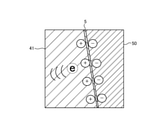
- FIG. 3 is a diagram showing an interface portion between a general pixel separation portion and silicon.
- FIG. 4 is a diagram showing an interface portion between the pixel separation portion and silicon according to the present disclosure.
- FIG. 5 is a diagram showing the movement of signal charges in the semiconductor layer according to the present disclosure.
- a trench is formed at a position where the pixel separation portion is formed on the silicon substrate 41, and after cleaning the silicon substrate 41, a metal oxide having an antireflection function such as aluminum oxide is embedded in the trench. Formed by
- the natural oxide film 5 has a very thin film thickness of 1 nm, holes (holes) are formed at the interface portion with the silicon substrate 41 due to the influence of the negatively charged pixel separation portion 50. ) Is excited to generate a hole current.
- the pixel array unit 21 is insulated between the pixel separation unit 50 and the silicon substrate 41 in the semiconductor layer 40 with a film thickness of 2 nm or more, which is thicker than that of the natural oxide film 5.
- a film 51 is provided.
- the pixel array unit 21 can widen the distance between the negatively charged pixel separation unit 50 and the silicon substrate 41, so that holes (holes) excited at the interface portion between the insulating film 51 and the silicon substrate 41 are excited. ) Can be reduced.
- the pixel array unit 21 photoelectric conversion is performed in the vicinity of the pixel separation unit 50 and the antireflection film 52 like the electrons shown by the dotted line in FIG. 5, and if the insulating film 51 is not present, the transfer is performed to the charge detection unit DET1.
- the difficult signal charge can be transferred to the charge detection unit DET1.
- the pixel array unit 21 can suppress a decrease in electron transfer efficiency.
- the depth of the pixel separation unit 50 is too deep, the distance between the pixel separation unit 50 and the charge detection units DET0 and DET1 becomes short, and the signal charge is attracted to the pixel separation unit 50 to charge the charge. Since the transfer efficiency is lowered, the depth of the pixel separation unit 50 is limited.
- the pixel array unit 21 is limited so that the depth D1 of the semiconductor layer 40 of the pixel separation unit 50 from the incident surface is 0.67 times or less the thickness D2 of the semiconductor layer 40. .. Therefore, for example, when the thickness of the semiconductor layer 40 is 6.7 ⁇ m, the depth of the pixel separation unit 50 is 4.5 ⁇ m or less.
- the pixel array unit 21 secures a distance between the pixel separation unit 50 and the charge detection units DET0 and DET1 to the extent that the signal charge transfer is not affected, thereby suppressing a decrease in electron transfer efficiency. Can be done.
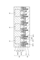
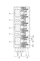
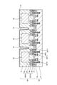
- FIGS. 6 to 9 are diagrams showing a manufacturing process of the pixel array according to the present disclosure.
- an N-type impurity is ion-implanted into a predetermined position inside from the surface (bottom surface) of the P-type silicon substrate 41 to perform an annealing treatment into the inside of the silicon substrate 41.
- the photoelectric conversion unit 42 and the charge detection units DET0 and DET1 are formed.
- the voltage application portions MIX0 and MIX1 are formed inside the silicon substrate 41 by ion-implanting P-type impurities into predetermined positions inside from the surface (lower surface) of the silicon substrate 41 and performing an annealing treatment. .. After that, a silicon oxide film 47 is formed between each charge detection unit DET0, DET1 and each voltage application unit MIX0, MIX1 to insulate.
- the multilayer wiring layer 30 is formed by sequentially laminating the interlayer insulating film 31 and the wiring pattern on the surface (lower surface) of the silicon substrate 41. Then, the silicon substrate 41 is ground and polished from the back surface side to make it thinner.
- a trench 70 is formed from the back surface side at the formation position of the pixel separation portion 50 (see FIG. 2) on the silicon substrate 41, and the silicon substrate 41 is washed.
- an insulating film is formed on the back surface (upper surface) of the silicon substrate 41 and the inner peripheral surface of the trench 70 so that the film thickness is 2 nm or more, for example, by forming a silicon oxide film.
- the film 51 is formed.
- the insulating film 51 can be extended from between the pixel separation portion 50 and the silicon substrate 41 to the incident surface of light on the silicon substrate 41.
- the signal charges photoelectrically converted in the vicinity of the back surface (upper surface) of the silicon substrate 41 can also be efficiently transferred to the charge detection units DET0 and DET1.
- the insulating film 51 is formed by, for example, ALD (Atomic Layer Deposition). As a result, the film thickness of the insulating film 51 can be accurately controlled at the atomic layer level.
- the film forming method of the insulating film 51 is not limited to the ALD.
- the insulating film 51 can also be formed by, for example, thermal oxidation, CVD (Chemical Vapor Deposition), plasma oxidation, ISSG (In-Situ-Steam Generation), or the like.
- the pixel separation unit 50 can also be formed of a material containing at least one of hafnium, zirconium, aluminum, tantalum, titanium, yttrium, and a lanthanoid element.
- the pixel separation unit 50 containing these elements can also prevent light from being reflected inside the semiconductor layer 40.
- the interlayer insulating films 61 and 62 are sequentially laminated on the antireflection film 52.
- the interlayer insulating films 61 and 62 are formed of, for example, silicon oxide or silicon nitride.
- the light-shielding member 65 is formed on the interlayer insulating film 62 at a position overlapping the pixel separation portion 50 in a plan view.
- a resin flattening film 63 is formed on the interlayer insulating film 62 and the light-shielding member 65, and the microlens 64 is laminated on the flattening film 63 to complete the pixel array portion 21 shown in FIG.
- a silicon oxide film is used as the insulating film 51 here, the insulating film 51 may be a silicon nitride film.
- the silicon nitride film has low ion conductivity, even if a natural oxide film is formed on the back surface (upper surface) of the silicon substrate 41 and the inner peripheral surface of the trench 70 by the cleaning process, the pixel separation portion 50 and the reflection from the natural oxide film are formed. It is possible to prevent the movement of oxygen ions O 2- to the prevention film 52. Further, when the silicon oxide film is used as the insulating film 51, the insulating film 51 can be formed at a lower cost than when silicon nitride is used.
- the insulating film 51 may be a metal oxide film having a positive fixed charge.
- the metal oxide film having a positive fixed charge includes, for example, at least one of yttrium oxide and lanthanum oxide.
- the insulating film 51 can also prevent holes from being excited at the interface portion of the silicon substrate 41 with the insulating film 51.
- the solid-state image sensor 1 has a plurality of photoelectric conversion units 42, a pair of voltage application units MIX0 and MIX1, charge detection units DET0 and DET1, a pixel separation unit 50, and an insulating film 51 having a film thickness of 2 nm or more. ..
- the plurality of photoelectric conversion units 42 are provided in a matrix on the semiconductor layer 40 in a plan view, and photoelectrically convert incident light into signal charges.
- the pair of voltage application units MIX0 and MIX1 are provided on the side of the semiconductor layer 40 opposite to the incident surface of light.
- the charge detection units DET0 and DET1 surround each voltage application unit MIX0 and MIX1 in a ring shape in a plan view, and detect signal charges distributed by alternately applying a predetermined voltage to the pair of voltage application units MIX0 and MIX1. ..
- the pixel separation unit 50 divides and separates the semiconductor layer 40 into each photoelectric conversion unit 42 in a plan view, and extends from the incident surface of light in the depth direction of the semiconductor layer 40.
- An insulating film having a film thickness of 2 nm or more is provided between the pixel separation portion 50 and the semiconductor layer 40.
- the solid-state image sensor 1 increases the distance between the pixel separation unit 50 and the silicon substrate 41 in the semiconductor layer 40, thereby causing image quality deterioration due to light leakage to the adjacent photoelectric conversion unit 42 and the photoelectric conversion unit. It is possible to suppress both deterioration of the charge transfer efficiency from the charge detection units DET0 and DET1 from 42.
- the depth of the light in the semiconductor layer 40 from the incident surface is 0.67 times or less the thickness of the semiconductor layer 40.
- the solid-state image sensor 1 suppresses a decrease in electron transfer efficiency by ensuring a distance between the pixel separation unit 50 and the charge detection units DET0 and DET1 to the extent that the signal charge transfer is not affected. Can be done.
- the insulating film 51 extends to the incident surface of light in the semiconductor layer 40.
- the solid-state image sensor 1 can efficiently transfer the signal charges photoelectrically converted in the vicinity of the back surface (upper surface) which is the light incident surface of the silicon substrate 41 to the charge detection units DET0 and DET1.
- the insulating film 51 is a silicon oxide film. As a result, the insulating film 51 can be formed at a lower cost than the silicon nitride film.
- the insulating film 51 is a silicon nitride film. Since the silicon nitride film has low ion conductivity, even if a natural oxide film is formed on the back surface (upper surface) of the silicon substrate 41 and the inner peripheral surface of the trench 70 by the cleaning process, the pixel separation portion 50 and the reflection from the natural oxide film are formed. It is possible to prevent the movement of oxygen ions O 2- to the prevention film 52.
- the insulating film 51 is a metal oxide film having a positive fixed charge.
- the solid-state image sensor 1 can suppress the excitation of holes at the interface portion of the silicon substrate 41 with the insulating film 51.
- the metal oxide film contains at least one of yttrium oxide and lanthanum oxide.
- the insulating film 51 is formed by ALD (Atomic Layer Deposition). As a result, the film thickness of the insulating film 51 can be accurately controlled at the atomic layer level.
- the pixel separation unit 50 contains at least one of hafnium, zirconium, aluminum, tantalum, titanium, yttrium, and a lanthanoid element. As a result, the pixel separation unit 50 can prevent light from being reflected inside the semiconductor layer 40.
- the present technology can also have the following configurations.
- a plurality of photoelectric conversion units provided in a matrix on the semiconductor layer in a plan view and photoelectrically convert incident light into signal charges.
- a pair of voltage application portions provided on the side of the semiconductor layer opposite to the incident surface of light,
- a charge detection unit that surrounds each voltage application unit in a ring shape in a plan view and detects the signal charge distributed by alternately applying a predetermined voltage to the pair of voltage application units.
- the semiconductor layer is partitioned and separated for each photoelectric conversion unit, and a pixel separation unit extending from the incident surface of the light in the depth direction of the semiconductor layer and a pixel separation unit.
- a solid-state image sensor provided between the pixel separation portion and the semiconductor layer and having an insulating film having a film thickness of 2 nm or more.
- the pixel separation unit is The solid-state image sensor according to (1), wherein the depth of the light from the incident surface of the semiconductor layer is 0.67 times or less the thickness of the semiconductor layer.
- the insulating film is The solid-state image sensor according to (1) or (2) above, which extends to the incident surface of the light in the semiconductor layer.
- the insulating film is The solid-state image sensor according to any one of (1) to (3) above, which is a silicon oxide film.
- the insulating film is The solid-state image sensor according to any one of (1) to (3) above, which is a silicon nitride film.
- the insulating film is The solid-state image sensor according to any one of (1) to (3) above, which is a metal oxide film having a positive fixed charge.
- the metal oxide film is The solid-state image sensor according to (6) above, which comprises at least one of yttrium oxide and lanthanum oxide.
- the insulating film is The solid-state image sensor according to any one of (1) to (7) above, which is formed by ALD (Atomic Layer Deposition).
- the pixel separation unit is The solid-state imaging device according to any one of (1) to (8) above, which comprises at least one of hafnium, zirconium, aluminum, tantalum, titanium, yttrium, and a lanthanoid element.
- Solid-state image sensor 21 Pixel array unit 22 Vertical drive unit 23 Column processing unit 24 Horizontal drive unit 25 System control unit 26 Signal processing unit 27 Data storage unit 30 Multi-layer wiring layer 31, 61, 62 Interlayer insulating film 32 Multi-layer wiring 40 Semiconductor layer 41 Silicon substrate 42 Photoconverter MIX0, MIX1 Voltage application part DET0, DET1 Charge detection part 50 Pixel separation part 51 Insulation film 52 Antireflection film 63 Flattening film 64 Microlens 65 Light-shielding member
Landscapes
- Solid State Image Pick-Up Elements (AREA)
Abstract
本開示に係る固体撮像装置(1)は、複数の光電変換部(42)と、一対の電圧印加部(MIX0,MIX1)と、電荷検出部(DET0,DET1)と、画素分離部(50)と、膜厚が2nm以上の絶縁膜(51)とを有する。光電変換部(42)は、平面視において半導体層に行列状に設けられ、入射する光を信号電荷に光電変換する。一対の電圧印加部(MIX0,MIX1)は、半導体層における光の入射面とは反対側に設けられる。電荷検出部(DET0,DET1)は、平面視において各電圧印加部を環状に囲み、一対の電圧印加部に所定の電圧が交互に印加されることによって振り分けられる信号電荷を検出する。画素分離部(50)は、平面視において半導体層を光電変換部毎に区画して分離し、光の入射面から半導体層の深さ方向に延在する。膜厚が2nm以上の絶縁膜(51)は、画素分離部と半導体層との間に設けられる。
Description
本開示は、固体撮像装置に関する。
間接ToF(Time of Flight)方式を利用した測距システムは、物体に向けて、例えば、赤外光などの照射光を照射し、その照射光が物体の表面で反射されて返ってくる反射光を固体撮像装置によって受光して検出する。そして、測距システムは、照射光を照射してから反射光を受光するまでの時間を位相差として検出し、位相差に基づいて物体までの距離を算出する。
固体撮像装置は、複数の受光画素が平面視において行列状に配列される画素アレイを備える。各受光画素は、入射する光を信号電荷に光電変換する光電変換部と、光電変換された信号電荷を一時的に保持する電荷蓄積部とを備える。
かかる固体撮像装置として、光電変換部毎に2つの電荷蓄積部を備え、光電変換した信号電荷を2つの電荷蓄積部に振分けるものがある。例えば、特許文献1には、光電変換部毎に設けられる一対の電圧印加部と、各電圧印加部を環状に囲み、一対の電圧印加部に所定の電圧が交互に印加されることによって振り分けられる信号電荷を検出する電荷検出部とを備える固体撮像装置が開示されている。
しかしながら、上記の従来技術では、隣接する光電変換部への漏れ光による画質劣化、および、光電変換部から電荷検出部への電荷転送効率の悪化の双方を抑制することが困難であった。
そこで、本開示では、隣接する光電変換部への漏れ光による画質劣化、および、光電変換部から電荷検出部への電荷転送効率の悪化の双方を抑制することができる固体撮像装置を提案する。
本開示によれば、固体撮像装置が提供される。固体撮像装置は、複数の光電変換部と、一対の電圧印加部と、電荷検出部と、画素分離部と、膜厚が2nm以上の絶縁膜とを有する。光電変換部は、平面視において半導体層に行列状に設けられ、入射する光を信号電荷に光電変換する。一対の電圧印加部は、前記半導体層における光の入射面とは反対側に設けられる。電荷検出部は、平面視において各前記電圧印加部を環状に囲み、前記一対の電圧印加部に所定の電圧が交互に印加されることによって振り分けられる前記信号電荷を検出する。画素分離部は、平面視において前記半導体層を前記光電変換部毎に区画して分離し、前記光の入射面から前記半導体層の深さ方向に延在する。膜厚が2nm以上の絶縁膜は、前記画素分離部と前記半導体層との間に設けられる。
以下に、本開示の実施形態について図面に基づいて詳細に説明する。なお、以下の各実施形態において、同一の部位には同一の符号を付することにより重複する説明を省略する。
[1.固体撮像装置の構成例]
本技術は、例えば間接ToF(Time of Flight)方式により測距を行う測距システムを構成する固体撮像装置や、そのような固体撮像装置を有する撮像装置などに適用することが可能である。
本技術は、例えば間接ToF(Time of Flight)方式により測距を行う測距システムを構成する固体撮像装置や、そのような固体撮像装置を有する撮像装置などに適用することが可能である。
例えば、測距システムは、車両に搭載され、車外にある対象物までの距離を測定する車載用のシステムや、ユーザの手等の対象物までの距離を測定し、その測定結果に基づいてユーザのジェスチャを認識するジェスチャ認識用のシステムなどに適用することができる。この場合、ジェスチャ認識の結果は、例えばカーナビゲーションシステムの操作等に用いることができる。
図1は、本開示に係る固体撮像装置の構成例を示す図である。図1に示す固体撮像装置1は、裏面照射型のCAPD(Current Assisted Photonic Demodulator)センサであり、測距機能を有する撮像装置に設けられている。
固体撮像装置1は、回路基板101と、回路基板101上に積層されるセンサ基板102とを備える。センサ基板102には、複数の受光画素(以下、単に「画素」と記載する)が平面視において行列状に配列される画素アレイ部21が設けられる。
回路基板101には、周辺回路が設けられる。周辺回路は、例えば垂直駆動部22、カラム処理部23、水平駆動部24、およびシステム制御部25等が設けられる。垂直駆動部22は、例えば、各画素において光電変換された信号電荷を処理する画素トランジスタ等を含む。なお、ここでは、回路基板101の構成要素と、センサ基板102の構成要素との接続関係の理解を容易にするため、各構成要素を同一平面上に記載している。
このように、固体撮像装置1は、画素アレイ部21の画素がセンサ基板102に設けられ、画素トランジスタが回路基板101に設けられることによって、電荷収集効率の向上と消費電力の低減とを可能とした。
回路基板101には、さらに信号処理部26およびデータ格納部27も設けられている。なお、信号処理部26およびデータ格納部27は、回路基板101と同じ基板上に搭載してもよいし、回路基板101とは別の基板上に配置するようにしてもよい。
画素アレイ部21は、受光した光量に応じた信号電荷を生成し、その信号電荷に応じた信号を出力する画素が行方向および列方向に、すなわち行列状に2次元配置された構成となっている。すなわち、画素アレイ部21は、画素毎に入射した光を光電変換し、その結果得られた信号電荷に応じた信号を出力する光電変換部を複数有している。
ここで、行方向とは画素行の画素の配列方向(すなわち、水平方向)をいい、列方向とは画素列の画素の配列方向(すなわち、垂直方向)をいう。つまり、行方向は図中、横方向であり、列方向は図中、縦方向である。
画素アレイ部21において、行列状の画素配列に対して、画素行毎に画素駆動線28が行方向に沿って配線され、各画素列に2つの垂直信号線29が列方向に沿って配線されている。例えば画素駆動線28は、画素から信号を読み出す際の駆動を行うための駆動信号を伝送する。なお、図1では、画素駆動線28について1本の配線として示しているが、1本に限られるものではない。画素駆動線28の一端は、垂直駆動部22の各行に対応した出力端に接続されている。
垂直駆動部22は、シフトレジスタやアドレスデコーダなどによって構成され、画素アレイ部21の各画素を全画素同時あるいは行単位等で駆動する。すなわち、垂直駆動部22は、垂直駆動部22を制御するシステム制御部25とともに、画素アレイ部21の各画素の動作を制御する駆動部を構成している。
垂直駆動部22による駆動制御に応じて画素行の各画素から出力される信号は、垂直信号線29を通してカラム処理部23に入力される。カラム処理部23は、各画素から垂直信号線29を通して出力される信号に対して所定の信号処理を行うとともに、信号処理後の画素信号を一時的に保持する。
具体的には、カラム処理部23は、信号処理としてノイズ除去処理やAD(Analog to Digital)変換処理などを行う。
水平駆動部24は、シフトレジスタやアドレスデコーダなどによって構成され、カラム処理部23の画素列に対応する単位回路を順番に選択する。この水平駆動部24による選択走査により、カラム処理部23において単位回路ごとに信号処理された画素信号が順番に出力される。
システム制御部25は、各種のタイミング信号を生成するタイミングジェネレータなどによって構成され、そのタイミングジェネレータで生成された各種のタイミング信号を基に、垂直駆動部22、カラム処理部23、および水平駆動部24などの駆動制御を行う。
信号処理部26は、少なくとも演算処理機能を有し、カラム処理部23から出力される画素信号に基づいて演算処理等の種々の信号処理を行う。データ格納部27は、信号処理部26での信号処理にあたって、その処理に必要なデータを一時的に格納する。
[2.画素アレイ部の断面構造]
次に、図2を参照し、画素アレイ部21の断面構造について説明する。図2は、本開示に係る画素アレイ部21の断面構造の説明図である。なお、図2には、画素アレイ部21のうち、3画素部分の断面を選択的に示している。
次に、図2を参照し、画素アレイ部21の断面構造について説明する。図2は、本開示に係る画素アレイ部21の断面構造の説明図である。なお、図2には、画素アレイ部21のうち、3画素部分の断面を選択的に示している。
図2に示すように、画素アレイ部21は、多層配線層30と、多層配線層30上に積層される半導体層40と、半導体層40上に順次積層される絶縁膜51、反射防止膜52、層間絶縁膜61,62、平坦化膜63、およびマイクロレンズ64を備える。
多層配線層30は、例えば、酸化シリコンによって形成される層間絶縁膜31と、層間絶縁膜31の内部に設けられる銅配線等の多層配線32とを含む。半導体層40は、例えば、ボロン等の不純物がドープされたP型のシリコン基板41と、シリコン基板41の内部に設けられる複数の光電変換部42と、電圧印加部MIX0,MIX1と、電荷検出部DET0,DET1とを含む。
光電変換部42は、シリコン基板41に、例えば、リン等のN型の不純物がイオン注入されて形成された領域である。光電変換部42は、平面視において半導体層40に行列状に設けられ、マイクロレンズ64によって集光されて入射する光を信号電荷に光電変換する。
電圧印加部MIX0,MIX1は、半導体層40における光の入射面とは反対側に設けられる。一対の電圧印加部MIX0,MIX1は、光電変換部42毎に設けられる。電圧印加部MIX0,MIX1は、シリコン基板41に、比較的高濃度のP型の不純物がイオン注入されたP+領域43と、P+領域43上を覆うように、比較的低濃度のP型の不純物がイオン注入されたP-領域44とを含む。
電荷検出部DET0は、一方の電圧印加部MIX0を平面視において環状に囲むように設けられる。電荷検出部DET1は、他方の電圧印加部MIX1を平面視において環状に囲むように設けられる。
電荷検出部DET0,DET1は、シリコン基板41に、比較的高濃度のN型の不純物がイオン注入されたN+領域45と、N+領域45上を覆うように、比較的低濃度のN型の不純物がイオン注入されたN-領域46とを含む。各P+領域43と、各N+領域45との間は、酸化シリコン膜47によって絶縁される。
また、画素アレイ部21は、平面視において半導体層40を光電変換部42毎に区画して分離し、光の入射面から半導体層40の深さ方向に延在する画素分離部50を備える。画素分離部50は、反射防止材料によって形成され、半導体層40上に積層される反射防止膜52と連続する。平坦化膜63の内部には、平面視において画素分離部50と重なる位置に、遮光部材65が設けられる。
図2に示すような構成の画素アレイ部21は、CAPD(Current Assisted Photonic Demodulator)と呼ばれる。CAPD型の画素アレイ部21は、光電変換部42毎に、3つの電荷蓄積部(フローティングディフュージョン)を備え、各光電変換部42内に流す電流の向きを切り換えることによって、光電変換された信号電荷を2つのフローティングディフュージョンに振り分ける。
ここで、かかるCAPD型の画素アレイ部21の動作について説明する。画素アレイ部21は、マイクロレンズ64によって集光される入射光を光電変換部42によって信号電荷となる電子に光電変換する。
その後、画素アレイ部21は、あるタイミングでは、電圧印加部MIX1に正の電圧(例えば、1.5V)を印加し、電圧印加部MIX0に0Vまたは負の電圧を印加する。これにより、光電変換部42の内部には、電圧印加部MIX1から電圧印加部MIX0に向かって電流が流れる。信号電荷の電子は、この電流によって発生する電界により電荷検出部DET1へ誘導され、電荷検出部DET1に取り込まれて検知される。
電荷検出部DET1は、多層配線32によって第1のフローティングディフュージョンに接続されており、検知した信号電荷を第1のフローティングディフュージョンへ転送する。信号電荷は、一時的に第1のフローティングディフュージョンで保持された後、カラム処理部23(図1参照)へ読み出される。
次のタイミングでは、画素アレイ部21は、電圧印加部MIX0に正の電圧(例えば、1.5V)を印加し、電圧印加部MIX1に0Vまたは負の電圧を印加する。これにより、光電変換部42の内部には、電圧印加部MIX0から電圧印加部MIX1に向かって電流が流れる。信号電荷の電子は、この電流によって発生する電界により電荷検出部DET0へ誘導され、電荷検出部DET0に取り込まれて検知される。
電荷検出部DET0は、多層配線32によって第2のフローティングディフュージョンに接続されており、検知した信号電荷を第2のフローティングディフュージョンへ転送する。信号電荷は、一時的に第2のフローティングディフュージョンで保持された後、カラム処理部23(図1参照)へ読み出される。
ここで、一般的なCAPD型の画素アレイでは、光電変換部に入射光が半導体層内で反射し、隣接する周囲の光電変換部へ漏れ光となって侵入して混色が発生することがある。混色が発生すると、撮像画像では、被写体のエッジ部分がぼやけて画質が劣化する。
これに対して、本開示に係る画素アレイ部21は、平面視において半導体層40を光電変換部42毎に区画して分離し、光の入射面から半導体層40の深さ方向に延在する画素分離部50を備える。画素分離部50は、例えば、酸化アルミニウム等の反射防止機能を有する金属酸化物によって形成される。
これにより、画素アレイ部21は、光電変換部42に入射光が半導体層40内で反射しても、画素分離部50によって、光が隣接する光電変換部42へ侵入することを防止することにより、混色の発生を抑制することができる。
ただし、画素アレイ部21は、単に、トレンチ状の画素分離部50が設けられるだけでは、光電変換部42から電荷検出部DET0,DET1への電子転送効率が低下する。そこで、画素アレイ部21は、画素分離部50と、半導体層40のシリコンとの間に、膜厚が2nm以上の絶縁膜51を備えることによって、電子転送効率の低下を抑制する。絶縁膜51は、例えば、シリコン酸化膜である。なお、絶縁膜51は、シリコン窒化膜であってもよい。
[3.絶縁膜による作用効果]
次に、図3~図5を参照し、膜厚が2nm以上の絶縁膜51が設けられることによる作用効果について説明する。図3は、一般的な画素分離部とシリコンとの界面部分を示す図である。図4は、本開示に係る画素分離部とシリコンとの界面部分を示す図である。図5は、本開示に係る半導体層内の信号電荷の動きを示す図である。
次に、図3~図5を参照し、膜厚が2nm以上の絶縁膜51が設けられることによる作用効果について説明する。図3は、一般的な画素分離部とシリコンとの界面部分を示す図である。図4は、本開示に係る画素分離部とシリコンとの界面部分を示す図である。図5は、本開示に係る半導体層内の信号電荷の動きを示す図である。
一般的な画素分離部は、シリコン基板41における画素分離部の形成位置にトレンチを形成し、シリコン基板41を洗浄した後に、トレンチへ例えば酸化アルミニウム等の反射防止機能を備えた金属酸化物を埋め込むことによって形成される。
このとき、図3に示すように、自然酸化膜5は、膜厚が1nmと非常に薄いため、負に帯電した画素分離部50の影響によって、シリコン基板41との界面部分にホール(正孔)を励起させホール電流を発生させる。
これにより、本来、電荷検出部DET0,DET1に取り込まれるべき光電変換された信号電荷(電子)の一部は、ホール電流引き寄せられ、電荷検出部DET0,DET1へ転送されない。したがって、図3に示す一般的な画素分離部50が設けられる場合には、混色は抑制できるが、電子転送効率が低下する。
そこで、図4に示すように、本開示に係る画素アレイ部21は、画素分離部50と半導体層40におけるシリコン基板41との間に、膜厚が自然酸化膜5よりも厚い2nm以上の絶縁膜51を備える。
これにより、画素アレイ部21は、負に帯電する画素分離部50とシリコン基板41との間隔を広げることができるので、絶縁膜51におけるシリコン基板41との界面部分に励起されるホール(正孔)を減少させることができる。
したがって、画素アレイ部21によれば、図5に点線で示す電子のように、画素分離部50および反射防止膜52の近傍で光電変換され、絶縁膜51がなければ電荷検出部DET1へ転送され難い信号電荷を電荷検出部DET1へ転送することができる。その結果、画素アレイ部21は、電子転送効率の低下を抑制することができる。
また、画素アレイ部21では、画素分離部50の深さが深すぎると、画素分離部50と電荷検出部DET0,DET1との距離が近くなり、信号電荷が画素分離部50に引き寄せられて電荷転送効率が低下するので、画素分離部50の深さに制限を設けている。
具体的には、画素アレイ部21では、画素分離部50の半導体層40における光の入射面からの深さD1が半導体層40の厚さD2の0.67倍以下となるように制限される。このため、例えば、半導体層40の厚さが6.7μmの場合、画素分離部50の深さは、4.5μm以下とされる。
これにより、画素アレイ部21は、信号電荷の転送に影響を及ぼさない程度まで、画素分離部50と電荷検出部DET0,DET1との距離を確保することによって、電子転送効率の低下を抑制することができる。
[4.画素アレイの製造方法]
次に、図6~図9を参照し、画素アレイ部21の製造方法について説明する。図6~図9は、本開示に係る画素アレイの製造工程を示す図である。
次に、図6~図9を参照し、画素アレイ部21の製造方法について説明する。図6~図9は、本開示に係る画素アレイの製造工程を示す図である。
図6にしめすように、まず、P型のシリコン基板41の表面(下面)から内部の所定位置に、それぞれN型の不純物をイオン注入してアニール処理を行うことによって、シリコン基板41の内部に、光電変換部42および電荷検出部DET0,DET1を形成する。
さらに、シリコン基板41の表面(下面)から内部の所定位置に、それぞれP型の不純物をイオン注入してアニール処理を行うことによって、シリコン基板41の内部に、電圧印加部MIX0,MIX1を形成する。その後、各電荷検出部DET0,DET1および各電圧印加部MIX0,MIX1の間に酸化シリコン膜47を形成して絶縁する。
続いて、シリコン基板41の表面(下面)に層間絶縁膜31および配線パターンを順次積層することによって、多層配線層30を形成する。そして、シリコン基板41を裏面側から研削および研磨して薄化させる。
その後、図7に示すように、シリコン基板41における画素分離部50(図2参照)の形成位置に、裏面側からトレンチ70を形成し、シリコン基板41を洗浄する。続いて、図8に示すように、シリコン基板41の裏面(上面)およびトレンチ70の内周面に、膜厚が2nm以上となるように、例えば、シリコン酸化膜を成膜することによって、絶縁膜51を形成する。
このように、絶縁膜51を画素分離部50とシリコン基板41との間からシリコン基板41における光の入射面まで延在させることができる。これにより、シリコン基板41の裏面(上面)近傍で光電変換される信号電荷についても、効率的に電荷検出部DET0,DET1へ転送させることができる。
また、絶縁膜51の成膜は、例えば、ALD(Atomic Layer Deposition)によって行う。これにより、原子層レベルで絶縁膜51の膜厚を正確にコントロールすることができる。なお、絶縁膜51の成膜方法は、ALDに限定されるものではない。
絶縁膜51は、例えば、熱酸化、CVD(Chemical Vapor Deposition)、プラズマ酸化、およびISSG(In-Situ-Steam Generation)等によっても成膜することができる。
その後、図9に示すように、シリコン基板41の裏面上およびトレンチ70の内部に、例えば、酸化アルミニウムを堆積させて、反射防止膜52および画素分離部50を形成する。なお、画素分離部50は、ハフニウム、ジルコニウム、アルミニウム、タンタル、チタン、イットリウム、およびランタノイド元素のうち、少なくともいずれか1つの元素を含む材料によって形成することもできる。これらの元素を含む画素分離部50によっても、半導体層40の内部で光が反射することを防止することができる。
続いて、反射防止膜52上に、層間絶縁膜61,62を順次積層する。層間絶縁膜61,62は、例えば、酸化シリコンまたは窒化シリコンによって形成する。そして、層間絶縁膜62上における平面視において画素分離部50と重なる位置に、遮光部材65を形成する。
その後、層間絶縁膜62および遮光部材65上に、樹脂製の平坦化膜63を形成し、平坦化膜63上にマイクロレンズ64を積層して、図2に示す画素アレイ部21が完成する。なお、ここでは、絶縁膜51としてシリコン酸化膜を使用したが、絶縁膜51は、シリコン窒化膜であってもよい。
シリコン窒化膜は、イオン電導性が低いため、洗浄工程によってシリコン基板41の裏面(上面)およびトレンチ70の内周面に自然酸化膜が形成されても、自然酸化膜から画素分離部50および反射防止膜52への酸素イオンO2-の移動を防止できる。また、絶縁膜51としてシリコン酸化膜を使用する場合には、窒化シリコンを使用する場合よりも低コストで絶縁膜51を形成することができる。
また、絶縁膜51は、正の固定電荷を有する金属酸化膜であってもよい。正の固定電荷を有する金属酸化膜は、例えば、イットリウム酸化物およびランタン酸化物の少なくともいずれか一方を含む。かかる絶縁膜51によっても、シリコン基板41における絶縁膜51との界面部分にホール(正孔)が励起されることを抑制することができる。
[5.効果]
固体撮像装置1は、複数の光電変換部42と、一対の電圧印加部MIX0,MIX1と、電荷検出部DET0,DET1と、画素分離部50と、膜厚が2nm以上の絶縁膜51とを有する。複数の光電変換部42は、平面視において半導体層40に行列状に設けられ、入射する光を信号電荷に光電変換する。一対の電圧印加部MIX0,MIX1は、半導体層40における光の入射面とは反対側に設けられる。電荷検出部DET0,DET1は、平面視において各電圧印加部MIX0,MIX1を環状に囲み、一対の電圧印加部MIX0,MIX1に所定の電圧が交互に印加されることによって振り分けられる信号電荷を検出する。画素分離部50は、平面視において半導体層40を光電変換部42毎に区画して分離し、光の入射面から半導体層40の深さ方向に延在する。膜厚が2nm以上の絶縁膜は、画素分離部50と半導体層40との間に設けられる。これにより、固体撮像装置1は、画素分離部50と半導体層40におけるシリコン基板41との間の距離を広げることにより、隣接する光電変換部42への漏れ光による画質劣化、および、光電変換部42から電荷検出部DET0,DET1への電荷転送効率の悪化の双方を抑制することができる。
固体撮像装置1は、複数の光電変換部42と、一対の電圧印加部MIX0,MIX1と、電荷検出部DET0,DET1と、画素分離部50と、膜厚が2nm以上の絶縁膜51とを有する。複数の光電変換部42は、平面視において半導体層40に行列状に設けられ、入射する光を信号電荷に光電変換する。一対の電圧印加部MIX0,MIX1は、半導体層40における光の入射面とは反対側に設けられる。電荷検出部DET0,DET1は、平面視において各電圧印加部MIX0,MIX1を環状に囲み、一対の電圧印加部MIX0,MIX1に所定の電圧が交互に印加されることによって振り分けられる信号電荷を検出する。画素分離部50は、平面視において半導体層40を光電変換部42毎に区画して分離し、光の入射面から半導体層40の深さ方向に延在する。膜厚が2nm以上の絶縁膜は、画素分離部50と半導体層40との間に設けられる。これにより、固体撮像装置1は、画素分離部50と半導体層40におけるシリコン基板41との間の距離を広げることにより、隣接する光電変換部42への漏れ光による画質劣化、および、光電変換部42から電荷検出部DET0,DET1への電荷転送効率の悪化の双方を抑制することができる。
また、画素分離部50は、半導体層40における光の入射面からの深さが半導体層40の厚さの0.67倍以下である。これにより、固体撮像装置1は、信号電荷の転送に影響を及ぼさない程度まで、画素分離部50と電荷検出部DET0,DET1との距離を確保することによって、電子転送効率の低下を抑制することができる。
また、絶縁膜51は、半導体層40における光の入射面上まで延在する。これにより、固体撮像装置1は、シリコン基板41の光入射面となる裏面(上面)近傍で光電変換される信号電荷についても、効率的に電荷検出部DET0,DET1へ転送させることができる。
また、絶縁膜51は、シリコン酸化膜である。これにより、シリコン窒化膜よりも低コストで絶縁膜51を形成することができる。
また、絶縁膜51は、シリコン窒化膜である。シリコン窒化膜は、イオン電導性が低いため、洗浄工程によってシリコン基板41の裏面(上面)およびトレンチ70の内周面に自然酸化膜が形成されても、自然酸化膜から画素分離部50および反射防止膜52への酸素イオンO2-の移動を防止できる。
また、絶縁膜51は、正の固定電荷を有する金属酸化膜である。これにより、固体撮像装置1は、シリコン基板41における絶縁膜51との界面部分にホール(正孔)が励起されることを抑制することができる。
また、金属酸化膜は、イットリウム酸化物およびランタン酸化物の少なくともいずれか一方を含む。これにより、固体撮像装置1は、シリコン基板41における絶縁膜51との界面部分にホール(正孔)が励起されることを抑制することができる。
また、絶縁膜51は、ALD(Atomic Layer Deposition)によって成膜される。これにより、原子層レベルで絶縁膜51の膜厚を正確にコントロールすることができる。
また、画素分離部50は、ハフニウム、ジルコニウム、アルミニウム、タンタル、チタン、イットリウム、およびランタノイド元素のうち、少なくともいずれか1つの元素を含む。これにより、画素分離部50は、半導体層40の内部で光が反射することを防止することができる。
なお、本明細書に記載された効果はあくまで例示であって限定されるものでは無く、また他の効果があってもよい。
なお、本技術は以下のような構成も取ることができる。
(1)
平面視において半導体層に行列状に設けられ、入射する光を信号電荷に光電変換する複数の光電変換部と、
前記半導体層における光の入射面とは反対側に設けられる一対の電圧印加部と、
平面視において各前記電圧印加部を環状に囲み、前記一対の電圧印加部に所定の電圧が交互に印加されることによって振り分けられる前記信号電荷を検出する電荷検出部と、
平面視において前記半導体層を前記光電変換部毎に区画して分離し、前記光の入射面から前記半導体層の深さ方向に延在する画素分離部と、
前記画素分離部と前記半導体層との間に設けられ、膜厚が2nm以上の絶縁膜と
を有する固体撮像装置。
(2)
前記画素分離部は、
前記半導体層における前記光の入射面からの深さが前記半導体層の厚さの0.67倍以下である
前記(1)に記載の固体撮像装置。
(3)
前記絶縁膜は、
前記半導体層における前記光の入射面上まで延在する
前記(1)または(2)に記載の固体撮像装置。
(4)
前記絶縁膜は、
シリコン酸化膜である
前記(1)~(3)のいずれかに記載の固体撮像装置。
(5)
前記絶縁膜は、
シリコン窒化膜である
前記(1)~(3)のいずれかに記載の固体撮像装置。
(6)
前記絶縁膜は、
正の固定電荷を有する金属酸化膜である
前記(1)~(3)のいずれかに記載の固体撮像装置。
(7)
前記金属酸化膜は、
イットリウム酸化物およびランタン酸化物の少なくともいずれか一方を含む
前記(6)に記載の固体撮像装置。
(8)
前記絶縁膜は、
ALD(Atomic Layer Deposition)によって成膜される
前記(1)~(7)のいずれかに記載の固体撮像装置。
(9)
前記画素分離部は、
ハフニウム、ジルコニウム、アルミニウム、タンタル、チタン、イットリウム、およびランタノイド元素のうち、少なくともいずれか1つの元素を含む
前記(1)~(8)のいずれかに記載の固体撮像装置。
(1)
平面視において半導体層に行列状に設けられ、入射する光を信号電荷に光電変換する複数の光電変換部と、
前記半導体層における光の入射面とは反対側に設けられる一対の電圧印加部と、
平面視において各前記電圧印加部を環状に囲み、前記一対の電圧印加部に所定の電圧が交互に印加されることによって振り分けられる前記信号電荷を検出する電荷検出部と、
平面視において前記半導体層を前記光電変換部毎に区画して分離し、前記光の入射面から前記半導体層の深さ方向に延在する画素分離部と、
前記画素分離部と前記半導体層との間に設けられ、膜厚が2nm以上の絶縁膜と
を有する固体撮像装置。
(2)
前記画素分離部は、
前記半導体層における前記光の入射面からの深さが前記半導体層の厚さの0.67倍以下である
前記(1)に記載の固体撮像装置。
(3)
前記絶縁膜は、
前記半導体層における前記光の入射面上まで延在する
前記(1)または(2)に記載の固体撮像装置。
(4)
前記絶縁膜は、
シリコン酸化膜である
前記(1)~(3)のいずれかに記載の固体撮像装置。
(5)
前記絶縁膜は、
シリコン窒化膜である
前記(1)~(3)のいずれかに記載の固体撮像装置。
(6)
前記絶縁膜は、
正の固定電荷を有する金属酸化膜である
前記(1)~(3)のいずれかに記載の固体撮像装置。
(7)
前記金属酸化膜は、
イットリウム酸化物およびランタン酸化物の少なくともいずれか一方を含む
前記(6)に記載の固体撮像装置。
(8)
前記絶縁膜は、
ALD(Atomic Layer Deposition)によって成膜される
前記(1)~(7)のいずれかに記載の固体撮像装置。
(9)
前記画素分離部は、
ハフニウム、ジルコニウム、アルミニウム、タンタル、チタン、イットリウム、およびランタノイド元素のうち、少なくともいずれか1つの元素を含む
前記(1)~(8)のいずれかに記載の固体撮像装置。
1 固体撮像装置
21 画素アレイ部
22 垂直駆動部
23 カラム処理部
24 水平駆動部
25 システム制御部
26 信号処理部
27 データ格納部
30 多層配線層
31,61 ,62 層間絶縁膜
32 多層配線
40 半導体層
41 シリコン基板
42 光電変換部
MIX0,MIX1 電圧印加部
DET0,DET1 電荷検出部
50 画素分離部
51 絶縁膜
52 反射防止膜
63 平坦化膜
64 マイクロレンズ
65 遮光部材
21 画素アレイ部
22 垂直駆動部
23 カラム処理部
24 水平駆動部
25 システム制御部
26 信号処理部
27 データ格納部
30 多層配線層
31,61 ,62 層間絶縁膜
32 多層配線
40 半導体層
41 シリコン基板
42 光電変換部
MIX0,MIX1 電圧印加部
DET0,DET1 電荷検出部
50 画素分離部
51 絶縁膜
52 反射防止膜
63 平坦化膜
64 マイクロレンズ
65 遮光部材
Claims (9)
- 平面視において半導体層に行列状に設けられ、入射する光を信号電荷に光電変換する複数の光電変換部と、
前記半導体層における光の入射面とは反対側に設けられる一対の電圧印加部と、
平面視において各前記電圧印加部を環状に囲み、前記一対の電圧印加部に所定の電圧が交互に印加されることによって振り分けられる前記信号電荷を検出する電荷検出部と、
平面視において前記半導体層を前記光電変換部毎に区画して分離し、前記光の入射面から前記半導体層の深さ方向に延在する画素分離部と、
前記画素分離部と前記半導体層との間に設けられ、膜厚が2nm以上の絶縁膜と
を有する固体撮像装置。 - 前記画素分離部は、
前記半導体層における前記光の入射面からの深さが前記半導体層の厚さの0.67倍以下である
請求項1に記載の固体撮像装置。 - 前記絶縁膜は、
前記半導体層における前記光の入射面上まで延在する
請求項1に記載の固体撮像装置。 - 前記絶縁膜は、
シリコン酸化膜である
請求項1に記載の固体撮像装置。 - 前記絶縁膜は、
シリコン窒化膜である
請求項1に記載の固体撮像装置。 - 前記絶縁膜は、
正の固定電荷を有する金属酸化膜である
請求項1に記載の固体撮像装置。 - 前記金属酸化膜は、
イットリウム酸化物およびランタン酸化物の少なくともいずれか一方を含む
請求項6に記載の固体撮像装置。 - 前記絶縁膜は、
ALD(Atomic Layer Deposition)によって成膜される
請求項1に記載の固体撮像装置。 - 前記画素分離部は、
ハフニウム、ジルコニウム、アルミニウム、タンタル、チタン、イットリウム、およびランタノイド元素のうち、少なくともいずれか1つの元素を含む
請求項1に記載の固体撮像装置。
Priority Applications (1)
| Application Number | Priority Date | Filing Date | Title |
|---|---|---|---|
| US18/004,784 US20230261022A1 (en) | 2020-07-20 | 2021-07-08 | Solid-state imaging device |
Applications Claiming Priority (2)
| Application Number | Priority Date | Filing Date | Title |
|---|---|---|---|
| JP2020-124051 | 2020-07-20 | ||
| JP2020124051 | 2020-07-20 |
Publications (1)
| Publication Number | Publication Date |
|---|---|
| WO2022019133A1 true WO2022019133A1 (ja) | 2022-01-27 |
Family
ID=79728695
Family Applications (1)
| Application Number | Title | Priority Date | Filing Date |
|---|---|---|---|
| PCT/JP2021/025748 Ceased WO2022019133A1 (ja) | 2020-07-20 | 2021-07-08 | 固体撮像装置 |
Country Status (2)
| Country | Link |
|---|---|
| US (1) | US20230261022A1 (ja) |
| WO (1) | WO2022019133A1 (ja) |
Citations (6)
| Publication number | Priority date | Publication date | Assignee | Title |
|---|---|---|---|---|
| JP2011054741A (ja) * | 2009-09-01 | 2011-03-17 | Toshiba Corp | 裏面照射型固体撮像装置 |
| JP2013089707A (ja) * | 2011-10-17 | 2013-05-13 | Sony Corp | 撮像素子、撮像装置、並びに、撮像装置および方法 |
| JP2015012043A (ja) * | 2013-06-26 | 2015-01-19 | 株式会社東芝 | 撮像装置およびその製造方法 |
| JP2017212453A (ja) * | 2017-07-11 | 2017-11-30 | ソニー株式会社 | 固体撮像装置、および、その製造方法、電子機器 |
| JP2020013906A (ja) * | 2018-07-18 | 2020-01-23 | ソニーセミコンダクタソリューションズ株式会社 | 受光素子および測距モジュール |
| WO2020017344A1 (ja) * | 2018-07-18 | 2020-01-23 | ソニーセミコンダクタソリューションズ株式会社 | 受光素子および測距モジュール |
-
2021
- 2021-07-08 WO PCT/JP2021/025748 patent/WO2022019133A1/ja not_active Ceased
- 2021-07-08 US US18/004,784 patent/US20230261022A1/en not_active Abandoned
Patent Citations (6)
| Publication number | Priority date | Publication date | Assignee | Title |
|---|---|---|---|---|
| JP2011054741A (ja) * | 2009-09-01 | 2011-03-17 | Toshiba Corp | 裏面照射型固体撮像装置 |
| JP2013089707A (ja) * | 2011-10-17 | 2013-05-13 | Sony Corp | 撮像素子、撮像装置、並びに、撮像装置および方法 |
| JP2015012043A (ja) * | 2013-06-26 | 2015-01-19 | 株式会社東芝 | 撮像装置およびその製造方法 |
| JP2017212453A (ja) * | 2017-07-11 | 2017-11-30 | ソニー株式会社 | 固体撮像装置、および、その製造方法、電子機器 |
| JP2020013906A (ja) * | 2018-07-18 | 2020-01-23 | ソニーセミコンダクタソリューションズ株式会社 | 受光素子および測距モジュール |
| WO2020017344A1 (ja) * | 2018-07-18 | 2020-01-23 | ソニーセミコンダクタソリューションズ株式会社 | 受光素子および測距モジュール |
Also Published As
| Publication number | Publication date |
|---|---|
| US20230261022A1 (en) | 2023-08-17 |
Similar Documents
| Publication | Publication Date | Title |
|---|---|---|
| US12317626B2 (en) | Photoelectric conversion apparatus and camera | |
| US11756976B2 (en) | Photoelectric conversion apparatus, camera, and moving body | |
| CN106229323B (zh) | 固态成像装置、固态成像装置的制造方法和电子设备 | |
| TWI241711B (en) | Solid state image sensing device, production method thereof, and method of driving solid state image sensing device | |
| CN102651375A (zh) | 固体摄像元件、固体摄像元件的制造方法和电子装置 | |
| JP2006173351A (ja) | 裏面入射型固体撮像装置及びその製造方法 | |
| US8659060B2 (en) | Solid-state imaging device and manufacturing method thereof | |
| CN105826331B (zh) | 采用背面深沟槽隔离的背照式图像传感器的制作方法 | |
| US20240030257A1 (en) | Imaging device and ranging device | |
| JP4972924B2 (ja) | 固体撮像装置およびその製造方法、並びにカメラ | |
| US11569279B2 (en) | Solid-state imaging device, method of manufacturing solid-state imaging device, and electronic apparatus | |
| US9159765B2 (en) | Apparatus for detecting soft X-ray radiation and X-ray detection system including such apparatus | |
| WO2022019133A1 (ja) | 固体撮像装置 | |
| US12477844B2 (en) | Photoelectric conversion apparatus, photoelectric conversion system using photoelectric conversion apparatus, and moving object | |
| US20230163152A1 (en) | Backside illuminated image sensor and method of manufacturing the same | |
| WO2023188891A1 (ja) | 光検出装置及び電子機器 | |
| TW202510313A (zh) | 光檢測裝置及其製造方法 | |
| JP6048483B2 (ja) | 固体撮像装置、および、その製造方法、電子機器 | |
| US20230393249A1 (en) | Sensor device and sensing module | |
| WO2023182517A1 (ja) | 半導体装置及び固体撮像装置 | |
| WO2021167060A1 (ja) | 固体撮像装置 | |
| CN117043953A (zh) | 摄像装置 |
Legal Events
| Date | Code | Title | Description |
|---|---|---|---|
| 121 | Ep: the epo has been informed by wipo that ep was designated in this application |
Ref document number: 21846510 Country of ref document: EP Kind code of ref document: A1 |
|
| NENP | Non-entry into the national phase |
Ref country code: DE |
|
| 122 | Ep: pct application non-entry in european phase |
Ref document number: 21846510 Country of ref document: EP Kind code of ref document: A1 |
|
| NENP | Non-entry into the national phase |
Ref country code: JP |