WO2022018861A1 - アルゴンベ-スの大気圧プラズマ処理方法及び大気圧プラズマ化学気相加工方法 - Google Patents
アルゴンベ-スの大気圧プラズマ処理方法及び大気圧プラズマ化学気相加工方法 Download PDFInfo
- Publication number
- WO2022018861A1 WO2022018861A1 PCT/JP2020/028462 JP2020028462W WO2022018861A1 WO 2022018861 A1 WO2022018861 A1 WO 2022018861A1 JP 2020028462 W JP2020028462 W JP 2020028462W WO 2022018861 A1 WO2022018861 A1 WO 2022018861A1
- Authority
- WO
- WIPO (PCT)
- Prior art keywords
- gas
- argon
- atmospheric pressure
- pressure plasma
- plasma
- Prior art date
- Legal status (The legal status is an assumption and is not a legal conclusion. Google has not performed a legal analysis and makes no representation as to the accuracy of the status listed.)
- Ceased
Links
Images

Classifications
-
- H—ELECTRICITY
- H05—ELECTRIC TECHNIQUES NOT OTHERWISE PROVIDED FOR
- H05H—PLASMA TECHNIQUE; PRODUCTION OF ACCELERATED ELECTRICALLY-CHARGED PARTICLES OR OF NEUTRONS; PRODUCTION OR ACCELERATION OF NEUTRAL MOLECULAR OR ATOMIC BEAMS
- H05H1/00—Generating plasma; Handling plasma
- H05H1/24—Generating plasma
Definitions
- the present invention relates to an argon-based atmospheric pressure plasma processing method and an atmospheric pressure plasma chemical vapor deposition processing method, and more specifically, it is possible to process the surface of a work such as a crystal with high quality using atmospheric pressure argon plasma.
- the present invention relates to an argon-based atmospheric pressure plasma processing method and an atmospheric pressure plasma chemical vapor deposition processing method.
- the vacuum vessel is exhausted to the ultimate pressure, and then the process gas is introduced to the predetermined pressure.
- the process gas pressure is set to a value of several 100 mPa to several tens of Pa, and a high frequency voltage of several 100 KHz to several tens of MHz is applied to the electrodes from the high frequency power supply (Patent Document 1).
- low-pressure plasma has excellent plasma stability, the material removal rate is low due to the low density of etchants.
- high vacuum equipment is required for the equipment, which also increases the size and cost of the equipment.
- etching and processing methods that use atmospheric pressure plasma.
- the basic principle of atmospheric pressure plasma chemical vaporization machining is described in Patent Document 2, and numerically controlled machining in which the machined electrode is machined by changing it relative to the machined surface.
- the method is described in Patent Document 3 and has been developed at Osaka University to which the present inventors belong.
- the AP-PCVM has the advantage that the partial pressure of the reaction gas is also high, so that the density of the etchant is high and the removal rate is high, and the vacuum equipment can be unnecessary or simplified, but the gas temperature is high. It becomes high and tends to shift to an arc discharge to reach a thermal equilibrium state, and when exposed to such plasma, it causes damage to the work. Therefore, it is necessary to maintain the plasma so that it does not shift to arc discharge, and to maintain a non-equilibrium state in which the gas temperature is sufficiently low, that is, the ion temperature is lower than the electron temperature.
- Non-Patent Document 1 a method of processing a crystal wafer, which is a material of a crystal oscillator, with high efficiency and high accuracy by using AP-PCVM has been proposed.
- helium gas which can easily generate plasma under atmospheric pressure, has been used as a carrier gas, but helium gas is expensive because it is 100% imported in Japan, and it is a strategy.
- Ar which can be industrially produced by fractional distillation of liquid air, as the carrier gas.
- argon since argon has a high breakdown voltage, there is a problem that electrons rapidly increase after the breakdown and an arc discharge that damages the crystal wafer is likely to occur.
- perfluorocarbon (PFC) gas particularly CF 4 is often used as the reaction gas.
- PFC perfluorocarbon
- the present inventors have found that even if the AP-PCVM, the addition of a small amount of ethanol in the process gas, together with the finding that the CF 4 containing Ar atmospheric pressure plasma can be stably generated, by the addition of ethanol , C-based products decomposed from ethanol are deposited on the surface of the work, solving a new problem that the etching process is hindered, and the present invention has been completed.
- the present invention provides an argon-based atmospheric pressure plasma processing method and an atmospheric pressure plasma chemical vapor deposition processing method, which are configured below, in order to solve the above-mentioned problems.
- an argon-based atmospheric pressure plasma treatment method in which the work surface is treated with an atmospheric pressure plasma generated by a process gas in which a carrier gas containing at least an argon gas and a reaction gas are mixed.
- a carrier gas a gas having an ionization potential smaller than that of the semi-stable level of argon is added, and a stabilizing gas that is ionized by the penning effect to generate electrons necessary for plasma generation and maintenance is added.
- argon-based atmospheric pressure plasma chemical gas phase processing method in which the work surface is etched by an atmospheric pressure plasma generated by a process gas in which a carrier gas containing at least an argon gas and a reaction gas are mixed.
- a carrier gas a gas having an ionization potential smaller than that of the semi-stable level of argon is added, and a stabilizing gas that is ionized by the penning effect to generate electrons necessary for generating and maintaining plasma is added, and the reaction is performed.
- argon-based atmospheric pressure plasma chemical gas phase processing characterized by adding a required amount of oxygen gas that acts on carbon generated in the etching process and can be vaporized and removed from the fluorogas.
- CF 4 when CF 4 is used as the reaction gas, stable plasma can be generated by adjusting the flow rate of argon, CF 4 , O 2, ethanol, the processing gap, and the like. We were able to find the optimum processing conditions in which twins do not occur in the quartz wafer. Further, when Ar is used as the carrier gas under the same conditions as compared with the case where the conventional He is used as the carrier gas, the same etching rate can be obtained.
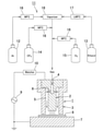
- FIG. 1 is a schematic diagram of an experimental setup used for AP-PCVM.
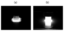
- FIG. 2A is an image of AP-PCVM on a crystal wafer by argon plasma without adding ethanol
- FIG. 2B is an image of AP-PCVM on a crystal wafer by argon plasma with ethanol added.
- 3 (a) to 3 (e) are photographs of removal spots formed on the crystal wafer by AP-PCVM using ethanol-added argon as a carrier gas
- FIGS. 3 (f) to 3 (j) are used in AP-PCVM.
- FIG. 3 (k) to 3 (o), are the X-ray photoelectron spectroscopy (XPS) measurement results of the plasma used in AP-PCVM.
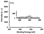
- FIG. 4 is an X-ray photoelectron spectroscopy (XPS) measurement result of the surface of the crystal wafer before the plasma treatment.
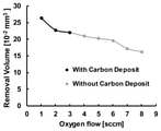
- FIG. 5 is a graph showing the amount of crystal wafer removed for 60 seconds at different O 2 flow rates.
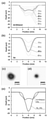
- FIG. 6 (a) shows a cross-sectional profile of the removal spots formed on the crystal wafer by AP-PCVM with a scanning white light interferometer (SWLI) using ethanol-added argon as the carrier gas, FIG. 6 (A).
- SWLI scanning white light interferometer
- FIG. 6 (c) is a carrier.
- FIG. 6 (d) is a 2D image of a removal spot formed by applying helium as a carrier gas
- FIG. 6 (e) is a carrier. It is a cross-sectional profile of a removal spot formed by etching for 45 seconds when using ethanol-added argon and helium as a gas.
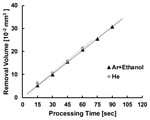
- FIG. 7 is a graph showing the relationship between the processing time and the removal amount of the removal spot formed by AP-PCVM (RF power: 60 W, ethanol: 0.003 g / min, carrier He / Ar: 600 sccm, CF 4). : 10 sccm, O 2 : 4 sccm).
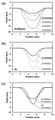
- FIG. 8 (a) shows a cross-sectional profile of a groove formed in a crystal wafer by AP-PCVM at different scanning rates using ethanol-added argon as the carrier gas
- FIG. 8 (b) uses helium as the carrier gas.
- FIG. 8 (a) shows a cross-sectional profile of a groove formed in a crystal wafer by AP-PCVM at different scanning rates using ethanol-added argon as the carrier gas
- FIG. 8 (b) uses helium as the carrier gas.
- FIG. 8 (b) uses helium as the carrier gas.
- FIG. 8 (c) is formed by etching at a scanning speed of 12 mm / min when using ethanol-added argon and helium as carrier gases. It is a cross-sectional profile of the groove.
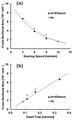
- FIG. 9 (a) is a graph showing the relationship between the scan rate and the cross-sectional area of the etched groove formed by the AP-PCVM
- FIG. 9 (b) is the residence time and the etched groove formed by the AP-PCVM.
- the present invention relates to an argon-based atmospheric pressure plasma treatment method for treating a work surface with an atmospheric pressure plasma generated by a process gas in which a carrier gas containing at least argon (Ar) gas and a reaction gas are mixed, as the carrier gas.
- Argon base characterized by adding a gas having an ionization potential smaller than that of the semi-stable level of argon and adding a stabilizing gas that is ionized by the penning effect to generate electrons necessary for the generation and maintenance of plasma. This is the atmospheric pressure plasma processing method.
- the stabilized gas is one or more selected from alcohol, hydrocarbon gas, and ammonia (NH 3).
- the alcohol include methanol, ethanol, propanol and the like.
- the hydrocarbon gas include methane, ethane, propane, butane and the like. Among them, ethanol is the most preferable because it is inexpensive and easy to handle.
- Table 1 shows the ionization potential and semi-stable energy of helium (He), argon (Ar), nitrogen (N 2 ), ethanol (C 2 H 5 OH) and ammonia (NH 3).
- the ionization potential of ethanol and ammonia is slightly lower than the metastable energy of argon. Ionization by the Penning effect occurs when the ionization potential of the target molecule is lower than the metastable energy of the excited atom or molecule.
- a reaction gas selected according to the purpose can be mixed with the process gas and applied to various plasma treatments.
- plasma treatment include etching, film formation, modification, oxidation and the like.
- AP-PCVM atmospheric pressure plasma chemical vaporization
- AP-PCVM turns the process gas into plasma in an atmospheric pressure atmosphere, causes an etchant (reaction species) consisting of generated neutral radicals and ions to act on the work surface, and removes volatile substances generated by a chemical reaction.
- etchant reaction species
- This is a method for processing the work surface with high precision.
- the "atmospheric pressure" in the present invention is not limited to the literal atmospheric pressure, but is a concept including a pressure in a slightly depressurized state performed to exhaust the process gas after use.
- the process gas consists of a carrier gas and a reaction gas.
- the carrier gas is mainly composed of an inert gas and has an action of diluting the reaction gas to generate and maintain a stable plasma.
- the reaction gas produces an etchant, and the etchant produces a volatile compound by a chemical reaction with the atoms constituting the work, and the etching process proceeds by removing the volatile compound from the surface of the work.
- PCVM limits the region to be etched by generating local plasma in a range sufficiently narrower than the machining region of the work, and numerically removes spots (machining marks) formed by local etching with respect to the machining region of the work. It is characterized by being able to partially control and scan and partially determine the amount of processing on the work surface, which is different from ordinary plasma etching that uniformly removes a wide area.
- a stabilizing gas that generates a large amount of electrons, it is possible to generate a glow discharge atmospheric pressure argon plasma that spreads stably and uniformly.
- a small amount of ethanol is added as a stabilizing gas.
- a processing experiment using AP-PCVM was performed using a mixed gas of argon and ethanol as the carrier gas, CF 4 and O 2 as the process gas, and a quartz wafer as the work. By applying the ethanol-containing process gas, a uniform and stable glow discharge plasma was generated, and good removal characteristics for correcting the thickness deviation of the quartz wafer were obtained.
- argon is used as the carrier gas, and in order to stabilize the argon plasma, an appropriate amount of ethanol is vaporized and mixed with argon.
- a fluorine-based gas capable of good etching on a work of a wide range of materials such as Si single crystal and Si compound is used.
- the fluorine-based gas is fluorine or a fluorine compound.
- the fluorine compound perfluorocarbon (PFC) gas or an inorganic fluorine compound can be satisfactorily used.
- the perfluorocarbon (PFC) gas is any one or more of CF 4 , C 2 F 6 , and C 3 F 8.
- the inorganic fluorine compound is any one or two of SF 6 and NF 3. Select the optimum reaction gas according to the material of the work.
- the crystal unit has good frequency temperature characteristics near room temperature. Furthermore, since the crystal unit is physically and chemically stable, the frequency change due to aging is small. Due to these excellent characteristics, crystal units are widely used in communication devices such as mobile phones and consumer devices such as digital cameras and computers in order to provide accurate reference signals. In order to increase the communication speed, it is necessary to reduce the thickness of the crystal wafer and increase the resonance frequency of the crystal oscillator. In recent commercial production of crystal units, wafer processes have been intensively developed to improve the productivity of the oscillators. In order to shorten the processing time of frequency adjustment and improve productivity, it is indispensable to make the thickness of the crystal wafer uniform.
- quartz wafers formed by conventional mechanical manufacturing processes such as wire saw cutting, wrapping, ion beam processing, and polishing typically have a thickness deviation of ⁇ 0.1%. .. This value is about 100 times the margin of error required for a crystal unit.
- AP-PCVM has been applied as a highly efficient and damage-free thickness correction technique to improve the thickness uniformity of quartz wafers.
- AP-PCVM is an ultra-precision modeling technology that uses fluorine radicals generated by atmospheric pressure plasma to transform the surface atoms of the work into volatile reaction products to form the desired shape.
- AP-PCVM is a non-contact chemical shaping technique that does not mechanically load the workpiece, thus preventing breakage of thin brittle materials and preventing the formation of subsurface damage (SSD) layers during the chemical removal process.
- SSD subsurface damage
- AP-PCVM is an atmospheric pressure process, no vacuum chamber is required.
- ICP inductively coupled plasma
- CCP capacitively coupled plasma
- plasma jet microwave plasma
- ICP and microwave plasmas generate hot gases above 200 ° C., increasing the likelihood of both crystal twins and quartz wafer breakage. Therefore, in this embodiment, the CCP is used in the AP-PCVM to process the quartz wafer.
- the thickness uniformity has been improved from 250 nm to 2 nm without forming SSD in one thickness correction process for commercially available crystal wafers, and it has already been used for electronic devices such as smartphones and wearables.
- the world's smallest crystal oscillator (1.0 x 0.8 mm) has been developed.
- AP-PCVM has used helium gas as a carrier gas so far.
- Helium gas used in industry is mainly produced from natural gas, and there are widespread concerns about problems such as depletion of natural resources and high cost.
- the present inventors have proposed using argon gas instead of helium gas as the carrier gas in the generation of atmospheric pressure plasma.
- Argon gas can be industrially produced by fractional distillation of liquid air, is easily available and inexpensive.
- the breakdown voltage for argon is much higher than the breakdown voltage for helium.
- the electrons increase rapidly after the breakdown, forming filamentary arc streamers.
- the addition of ethanol to argon has proven to be very useful for producing atmospheric pressure glow discharge plasmas.
- argon was used as the carrier gas for AP-PCVM together with a small amount of ethanol instead of helium. Ethanol AP-PCVM using argon based atmospheric CF 4 plasma was added by investigating the etching characteristics of the crystal wafer experiment was conducted.
- FIG. 1 shows an experimental setup of AP-PCVM.
- the electrode nozzle 1 has a structure in which an insulating ceramic cover 3 is coaxially arranged around the electrode 2 arranged in the center, and a gas supply hole 4 provided in the center on the base end side of the electrode 2 is provided. Is.
- a gas flow path 5 is provided between the electrode 2 and the cover 3, communicates with the gas supply hole 4 through a branch hole 6, and the process gas supplied from the gas supply hole 4 passes through the branch hole 6 to the gas flow path. It is supplied to 5.
- the tip of the electrode 2 is set at a position retracted by 3 mm from the tip of the cover 3, and a predetermined gap is set between the work 8 held on the work table 7 and the tip of the cover 3.
- High-frequency power is applied to the electrode 2 from the high-frequency power supply 9 via the matching unit 10, and the work table 7 is grounded.
- the electrode 2 is made of an aluminum alloy
- the cover 3 is made of alumina (Al 2 O 3 ).
- the frequency of the high frequency power supply 9 is a radio frequency (RF) of 13.56 MHz.
- the gas supply system 11 has four channels, one for carrier gas, one for ethanol, and two for reaction gas (CF 4 and O 2 ).
- reference numeral 12 indicates an argon gas cylinder
- 13 indicates an ethanol container
- 14 indicates a CF 4 gas cylinder
- 15 indicates an oxygen gas cylinder.
- the flow rates of the argon gas and the reaction gas were controlled using a mass flow controller (MFC) 16.
- MFC mass flow controller
- Ethanol concentration 99.5%
- LMFC liquid mass flow controller
- Argon gas mixed with ethanol by this gas-liquid mixing vaporization method and reaction gas (CF 4 and O 2 ) are mixed and supplied to the gas supply hole 4 as a process gas.
- an AT-cut crystal wafer (size: 54 mm ⁇ 50 mm ⁇ 90 ⁇ m) was used.
- the following AP-PCVM experiments were performed at room temperature (23.3 ° C.) without heating the quartz wafer. Further, the crystal wafer was held on the work table 7 by a vacuum chuck.
- the diameter of the electrode is 3 mm
- the distance between the tip of the electrode 2 and the crystal wafer (work 8) is 3.5 mm
- the distance between the tip of the cover 3 and the crystal wafer is 0.5 mm.
- a radio frequency (RF) power of 13.56 MHz is applied between the electrode 2 and the work table 7 from the high frequency power source 9, and argon at atmospheric pressure is applied in the space near the tip of the electrode 2 and between the work 8.
- RF radio frequency
- Fluorine radicals which are thought to be the etchants that etch quartz, are generated by the dissociation of CF 4 in atmospheric pressure argon plasma.
- FIG. 2A shows a photograph of argon plasma generated on a quartz wafer without the addition of ethanol.
- the breakdown voltage of argon was high, filamentary arc streamers were formed, and the high temperature caused by local arc discharge easily damaged the quartz wafer. Moreover, since the state of the local arc discharge was unstable, the reproducibility of the removal spot formation was low.
- FIG. 2 (b) shows a photograph of an ethanol-added argon plasma generated on a quartz wafer. The addition of ethanol formed a stable glow discharge plasma without filamentary arc streamers and did not break the quartz wafer. The reproducibility of removal spot formation has also improved. Therefore, it is possible to accurately correct the thickness distribution of the quartz wafer by numerically controlled AP-PCVM using argon to which ethanol is added instead of helium as the carrier gas.
- ethanol flow rate 0.003 g / min
- Ar 600 sccm
- the reaction gas is CF 4 (10 sccm) and O 2 (0 to 8 sccm)
- the RF power 60 W.
- the flow rate of ethanol determines the flow rate of argon according to the specifications of the electrode nozzle 1, and under the condition that the RF power is fixed at 60 W, plasma is stably generated, and the shape stability of the removal spot (machining mark) is stable.
- the minimum value was decided in consideration of the above.
- FIG. 3 shows the measurement results at oxygen flow rates of 0, 1, 2, 3, and 4 sccm, and photographs of removal spots of the crystal wafer formed by AP-PCVM using ethanol-added argon as a carrier gas in order from the left.
- FIG. 3 (a)-(e) shows emission spectroscopy (OES) spectra
- FIGS. 3 (f)-(j) emission spectroscopy (OES) spectra
- XPS X-ray photoelectron spectroscopy
- FIGS. 3 (b), (g), and (l) the case where 1 sccm of oxygen is added to the process gas is shown in FIGS. 3 (b), (g), and (l). Carbon deposits are still present, but their color is lighter and the deposit area is smaller. The emission of the C 2 swan band was weak compared to the OES spectrum of the plasma without the addition of oxygen. The XPS measurement results show that the CC peak is weakened. It is considered that a part of the incompletely decomposed carbon was oxidized by adding oxygen to the process gas. Thus, it is predicted that the addition of oxygen can suppress the formation of carbon deposits on the quartz surface.
- FIG. 4 is an XPS spectrum of the crystal wafer before plasma treatment, and since this result is almost the same as the XPS spectrum when the oxygen flow rate is 4 sccm (FIG. 3 (o)), the carbon deposit disappears. You can see that it is doing.
- FIG. 5 shows the relationship between the etching rate of the quartz wafer and the oxygen flow rate.
- the oxygen flow rate was changed from 1 to 8 sccm, and other processing conditions were fixed as described above.
- the processing time is 60 seconds.
- the O 2 is added 4 sccm, carbon deposits that are described above which has lost.
- the etching rate decreased.
- Oxygen itself does not contribute to the etching reaction of the crystal, and the generation of both O and F radicals requires energy from the active argon, so due to the competition between O 2 and CF 4 , the oxygen fraction is high. It is considered that the cause is that the etching rate decreases.
- the flow rate of argon was fixed at 600 sccm
- the flow rate of ethanol was fixed at 0.003 g / min
- the flow rate of CF 4 was fixed at 10 sccm
- the flow rate of O 2 was fixed at 4 sccm
- the RF power was fixed at 60 W.
- the helium-based process gas is He (flow rate: 600 sccm), CF 4 (flow rate: 10 sccm), and O 2 (flow rate: 4 sccm).
- the RF power is 60 W and the processing time is 15 to 90 seconds.
- FIG. 6 (a) shows the cross-sectional profile of the removal spots formed on the crystal wafer by AP-PCVM at different treatment times using argon (argon-based) with ethanol added as the carrier gas
- FIG. 6 (b). Show the cross-sectional profile of the removal spots formed on the crystal wafer by AP-PCVM at different processing times using helium (helium base) as the carrier gas.
- a scan of a white light interferometer (SWLI) image of a removal spot formed by etching helium and argon with ethanol as a carrier gas for 45 seconds and a comparison of cross-sectional profiles are shown in FIGS. 6 (c) to 6 (c). Shown in e).
- SWLI white light interferometer
- FIG. 6 (c) is a white light interferometer (SWLI) image of the argon-based removal spot
- FIG. 6 (d) is a white light interferometer (SWLI) image of the helium-based removal spot
- FIG. 6 (e). ) Show the cross-sectional profile of both removal spots.
- SWLI white light interferometer
- FIG. 7 shows the relationship between the removal amount of the removal spot and the processing time. It was found that the amount of removal using the argon-based and helium-based plasmas was almost the same in the same treatment time. In both cases, the removal amount was proportional to the processing time. The above results show that the same etching rate can be obtained and the operating cost can be reduced by using argon with ethanol added as the carrier gas of AP-PCVM instead of helium.
- the cross-sectional profile of the removal spot may affect the generation of twins in quartz processing.
- the cross-sectional profile of the steep and deep removal spot is obtained, but it is assumed that the temperature gradient of the quartz wafer becomes large, which increases the thermal stress and easily induces twinning. In other words, when processing quartz while suppressing the generation of twins, the removal rate cannot be increased so much.
- the cross-sectional profile of the removal spot is wide and shallow, the temperature gradient of the quartz wafer is small, and the thermal stress can be inferred to be small, and it is assumed that twinning is unlikely to be induced. That is, it is a remarkable feature that the argon-based AP-PCVM may be able to correct the thickness without twinning even if the removal rate is increased.
- the helium-based process gas is He (flow rate: 600 sccm), CF 4 (flow rate: 10 sccm), and O 2 (flow rate: 4 sccm). Both RF powers are 60W. Scan speeds are 3, 6, 9, and 12 mm / min.
- FIG. 8 (a) shows a cross-sectional profile of a groove formed in a quartz wafer in an AP-PCVM at different scan rates using an argon-based plasma
- FIG. 8 (b) shows a helium-based plasma. It is used to show the cross-sectional profile of the grooves formed in the quartz wafer during AP-PCVM at different scan rates.
- FIG. 8 (c) shows a comparison of cross-sectional profiles of grooves formed by etching at a scanning speed of 12 mm / min when an argon-based plasma is used and when a helium-based plasma is used.
- the removal spot was formed by the argon-based plasma treatment, the central cross-sectional shape of the removal spot became complicated as shown in FIG. 6, but in the case of the line scan experiment, the argon-based plasma treatment is also the helium-based plasma treatment.
- the grooves formed by the AP-PCVM were smoothed by the integration of the removal spot shapes along the scanning direction.
- FIG. 9A shows the relationship between the cross-sectional area of the groove formed in the crystal wafer by the line scan in AP-PCVM and the scanning speed. This result shows that the cross-sectional area correlates with the scan rate. Since the reciprocal of the scanning speed is regarded as the residence time of plasma, the relationship between the residence time and the cross-sectional area of the groove is shown in FIG. 9 (b). It was found that the cross-sectional area of the groove is proportional to the residence time of the plasma.
- argon has a higher breakdown voltage than helium, a filament arc streamer may be formed and the crystal wafer may be destroyed. Therefore, the thickness of the crystal wafer is increased by using argon as the carrier gas in AP-PCVM.
- the distribution of helium has not been modified so far.
- the present invention is widely and industrially applicable not only to the processing of quartz but also to the processing of Si single crystals or Si compounds.
- the Si compound include Si oxide and quartz, which can be applied to the processing of SiO 2 glass and thin films.
- it is also applicable to machining of SiC and Si 3 N 4. Specifically, it can be applied to the thickness correction of a crystal wafer and used in a process of manufacturing a high-precision crystal oscillator. Further, it can be applied to the thickness correction of the SiC wafer and used in the process of manufacturing a power device.
- the present invention can be applied to other than the method of directly removing the work by converting it into a volatile compound by an etching process.
- it can be applied to plasma-assisted polishing that modifies the surface of a hard and brittle difficult-to-process material to facilitate polishing.
- plasma-assisted polishing plasma generated by a process gas of argon, ethanol, and CF 4 (or SF 6 , NF 3 ) is applied to AlN (aluminum nitride) to apply AlF 3 (aluminum fluoride). Polishing can be facilitated if it is modified to.
- the technology for stabilizing atmospheric pressure argon plasma is plasma-assisted polishing that oxidizes SiC and facilitates polishing using a process gas in which O 2 or H 2 O is added as a reaction gas to argon and ethanol (). It is also applicable to Patent No. 5614677).
- Electrode nozzle 1 Electrode nozzle 2 Electrode 3 Cover 4 Gas supply hole 5 Gas flow path 6 Branch hole 7 Work table 8 Work 9 High frequency power supply 10 Matcher 11 Gas supply system 12 Argon gas cylinder 13 Ethanol container 14 CF 4 Gas cylinder 15 Oxygen gas cylinder 16 Mass flow controller ( MFC) 17 Liquid Mass Flow Controller (LMFC) 18 Liquid vaporizer
Landscapes
- Physics & Mathematics (AREA)
- Engineering & Computer Science (AREA)
- Plasma & Fusion (AREA)
- Spectroscopy & Molecular Physics (AREA)
- Drying Of Semiconductors (AREA)
Priority Applications (2)
| Application Number | Priority Date | Filing Date | Title |
|---|---|---|---|
| JP2022538557A JPWO2022018861A1 (cg-RX-API-DMAC7.html) | 2020-07-22 | 2020-07-22 | |
| PCT/JP2020/028462 WO2022018861A1 (ja) | 2020-07-22 | 2020-07-22 | アルゴンベ-スの大気圧プラズマ処理方法及び大気圧プラズマ化学気相加工方法 |
Applications Claiming Priority (1)
| Application Number | Priority Date | Filing Date | Title |
|---|---|---|---|
| PCT/JP2020/028462 WO2022018861A1 (ja) | 2020-07-22 | 2020-07-22 | アルゴンベ-スの大気圧プラズマ処理方法及び大気圧プラズマ化学気相加工方法 |
Publications (1)
| Publication Number | Publication Date |
|---|---|
| WO2022018861A1 true WO2022018861A1 (ja) | 2022-01-27 |
Family
ID=79729352
Family Applications (1)
| Application Number | Title | Priority Date | Filing Date |
|---|---|---|---|
| PCT/JP2020/028462 Ceased WO2022018861A1 (ja) | 2020-07-22 | 2020-07-22 | アルゴンベ-スの大気圧プラズマ処理方法及び大気圧プラズマ化学気相加工方法 |
Country Status (2)
| Country | Link |
|---|---|
| JP (1) | JPWO2022018861A1 (cg-RX-API-DMAC7.html) |
| WO (1) | WO2022018861A1 (cg-RX-API-DMAC7.html) |
Cited By (1)
| Publication number | Priority date | Publication date | Assignee | Title |
|---|---|---|---|---|
| WO2023237271A1 (de) * | 2022-06-08 | 2023-12-14 | Fraunhofer-Gesellschaft zur Förderung der angewandten Forschung e.V. | Ringförmige vorrichtung zum erzeugen von beschleunigten elektronen |
Citations (3)
| Publication number | Priority date | Publication date | Assignee | Title |
|---|---|---|---|---|
| JPH0785997A (ja) * | 1993-09-20 | 1995-03-31 | Ii C Kagaku Kk | 大気圧グロ−放電プラズマ処理法 |
| WO2009113402A1 (ja) * | 2008-03-13 | 2009-09-17 | 積水化学工業株式会社 | シリコン含有膜のエッチング方法および装置 |
| JP2010013735A (ja) * | 2009-09-29 | 2010-01-21 | Konica Minolta Holdings Inc | 樹脂フィルムの製造方法及び該樹脂フィルムを用いた有機エレクトロルミネッセンス素子 |
-
2020
- 2020-07-22 JP JP2022538557A patent/JPWO2022018861A1/ja active Pending
- 2020-07-22 WO PCT/JP2020/028462 patent/WO2022018861A1/ja not_active Ceased
Patent Citations (3)
| Publication number | Priority date | Publication date | Assignee | Title |
|---|---|---|---|---|
| JPH0785997A (ja) * | 1993-09-20 | 1995-03-31 | Ii C Kagaku Kk | 大気圧グロ−放電プラズマ処理法 |
| WO2009113402A1 (ja) * | 2008-03-13 | 2009-09-17 | 積水化学工業株式会社 | シリコン含有膜のエッチング方法および装置 |
| JP2010013735A (ja) * | 2009-09-29 | 2010-01-21 | Konica Minolta Holdings Inc | 樹脂フィルムの製造方法及び該樹脂フィルムを用いた有機エレクトロルミネッセンス素子 |
Cited By (1)
| Publication number | Priority date | Publication date | Assignee | Title |
|---|---|---|---|---|
| WO2023237271A1 (de) * | 2022-06-08 | 2023-12-14 | Fraunhofer-Gesellschaft zur Förderung der angewandten Forschung e.V. | Ringförmige vorrichtung zum erzeugen von beschleunigten elektronen |
Also Published As
| Publication number | Publication date |
|---|---|
| JPWO2022018861A1 (cg-RX-API-DMAC7.html) | 2022-01-27 |
Similar Documents
| Publication | Publication Date | Title |
|---|---|---|
| KR102691272B1 (ko) | 부바이어스를 사용하는 peald로 막을 증착하는 방법 | |
| JP6568822B2 (ja) | エッチング方法 | |
| CN101515542B (zh) | 用硫基蚀刻剂等离子体蚀刻含碳层 | |
| US11060189B2 (en) | Method to enable high temperature processing without chamber drifting | |
| TWI686862B (zh) | 多孔質膜之蝕刻方法 | |
| KR20180137030A (ko) | 고온에서 프로세싱 챔버 내의 붕소-탄소 잔류물들을 제거하기 위한 세정 프로세스 | |
| JP7485870B2 (ja) | プラズマ処理のための3フェーズパルス印加システム及び方法 | |
| US11773484B2 (en) | Hard mask deposition using direct current superimposed radio frequency plasma | |
| Sun et al. | Etching characteristics of quartz crystal wafers using argon-based atmospheric pressure CF4 plasma stabilized by ethanol addition | |
| CN110835748B (zh) | 沉积氮化硅的方法和设备 | |
| KR20210019398A (ko) | 에칭 방법 및 플라즈마 처리 장치 | |
| KR102436614B1 (ko) | 피처리체를 처리하는 방법 | |
| JP2024113055A (ja) | プラズマエッチング方法 | |
| US7833911B2 (en) | Method of manufacturing semiconductor device, apparatus of manufacturing semiconductor device and semiconductor device | |
| JP3649650B2 (ja) | 基板エッチング方法、半導体装置製造方法 | |
| KR20220097483A (ko) | 재료 표면 거칠기를 감소시키기 위한 방법들 | |
| US7344996B1 (en) | Helium-based etch process in deposition-etch-deposition gap fill | |
| KR20240137719A (ko) | 드라이 에칭 방법, 드라이 에칭제, 및 그 보존 용기 | |
| KR20240052809A (ko) | 탄소 함유 층을 에칭하기 위한 방법 및 장치 | |
| JPWO2010016249A1 (ja) | 半導体装置の製造方法およびプラズマエッチング装置 | |
| JPH08330278A (ja) | 表面処理方法および表面処理装置 | |
| CN112437973A (zh) | 等离子处理方法 | |
| US20260052919A1 (en) | Selective etching of silicon-containing material | |
| US20260052918A1 (en) | Selective etching of silicon-and-germanium-containing material | |
| CN121358192A (zh) | 一种半导体的刻蚀方法及等离子体设备 |
Legal Events
| Date | Code | Title | Description |
|---|---|---|---|
| 121 | Ep: the epo has been informed by wipo that ep was designated in this application |
Ref document number: 20945859 Country of ref document: EP Kind code of ref document: A1 |
|
| ENP | Entry into the national phase |
Ref document number: 2022538557 Country of ref document: JP Kind code of ref document: A |
|
| NENP | Non-entry into the national phase |
Ref country code: DE |
|
| 122 | Ep: pct application non-entry in european phase |
Ref document number: 20945859 Country of ref document: EP Kind code of ref document: A1 |