WO2022013987A1 - 通信装置、通信方法、通信システムおよび通信プログラム - Google Patents
通信装置、通信方法、通信システムおよび通信プログラム Download PDFInfo
- Publication number
- WO2022013987A1 WO2022013987A1 PCT/JP2020/027563 JP2020027563W WO2022013987A1 WO 2022013987 A1 WO2022013987 A1 WO 2022013987A1 JP 2020027563 W JP2020027563 W JP 2020027563W WO 2022013987 A1 WO2022013987 A1 WO 2022013987A1
- Authority
- WO
- WIPO (PCT)
- Prior art keywords
- parent
- communication device
- optical
- communication
- child
- Prior art date
- Legal status (The legal status is an assumption and is not a legal conclusion. Google has not performed a legal analysis and makes no representation as to the accuracy of the status listed.)
- Ceased
Links
Images




Classifications
-
- H—ELECTRICITY
- H04—ELECTRIC COMMUNICATION TECHNIQUE
- H04B—TRANSMISSION
- H04B10/00—Transmission systems employing electromagnetic waves other than radio-waves, e.g. infrared, visible or ultraviolet light, or employing corpuscular radiation, e.g. quantum communication
- H04B10/27—Arrangements for networking
- H04B10/275—Ring-type networks
-
- H—ELECTRICITY
- H04—ELECTRIC COMMUNICATION TECHNIQUE
- H04B—TRANSMISSION
- H04B10/00—Transmission systems employing electromagnetic waves other than radio-waves, e.g. infrared, visible or ultraviolet light, or employing corpuscular radiation, e.g. quantum communication
- H04B10/03—Arrangements for fault recovery
-
- H—ELECTRICITY
- H04—ELECTRIC COMMUNICATION TECHNIQUE
- H04J—MULTIPLEX COMMUNICATION
- H04J14/00—Optical multiplex systems
- H04J14/08—Time-division multiplex systems
-
- H—ELECTRICITY
- H04—ELECTRIC COMMUNICATION TECHNIQUE
- H04L—TRANSMISSION OF DIGITAL INFORMATION, e.g. TELEGRAPHIC COMMUNICATION
- H04L12/00—Data switching networks
- H04L12/28—Data switching networks characterised by path configuration, e.g. LAN [Local Area Networks] or WAN [Wide Area Networks]
- H04L12/42—Loop networks
- H04L12/427—Loop networks with decentralised control
- H04L12/43—Loop networks with decentralised control with synchronous transmission, e.g. time division multiplex [TDM], slotted rings
-
- H—ELECTRICITY
- H04—ELECTRIC COMMUNICATION TECHNIQUE
- H04L—TRANSMISSION OF DIGITAL INFORMATION, e.g. TELEGRAPHIC COMMUNICATION
- H04L12/00—Data switching networks
- H04L12/28—Data switching networks characterised by path configuration, e.g. LAN [Local Area Networks] or WAN [Wide Area Networks]
- H04L12/42—Loop networks
- H04L12/437—Ring fault isolation or reconfiguration
Definitions
- the present invention relates to a technique for performing communication by time-dividing and multiplexing optical signals in an optical ring network constituting a communication system.
- optical signals of wavelengths assigned in advance to each of a plurality of optical transmission devices connected to the optical ring network are multiplexed and communicated by OADM (Optical add-drop multiplexer) technology.
- OADM Optical add-drop multiplexer
- a burst optical ring network technology that transmits an optical signal by time division multiplexing instead of an OADM is known.
- one optical transmission device operates as a master device and the other optical transmission device operates as a child device among a plurality of optical transmission devices connected to an optical ring network.
- the parent device controls the data transmission timing of the child device including the own device and registers the child device newly connected to the optical ring network.
- the plurality of optical transmission devices connected to the optical ring network can communicate by time-dividing and multiplexing optical signals by the burst optical ring network technology.
- the child device operates as a new parent device when the parent device that controls a plurality of optical transmission devices connected to an optical ring network that communicates by time-dividing and multiplexing optical signals cannot operate normally. It is an object of the present invention to provide a communication device, a communication method, a communication system, and a communication program capable of continuing system operation.
- the communication device of the present invention is connected to an optical ring network, communicates optical signals by time-division multiplexing, and receives control signals for controlling the transmission timing of optical signals from a parent communication device.
- control signal is not received within a predetermined period, it is determined that the parent communication device is not operating normally, and the device has a determination unit for operating the own device as a new parent communication device. It is a feature.
- the present invention is a communication method used in a communication system connected by an optical ring network with one of a plurality of communication devices as a parent communication device and the other as a child communication device, and the parent communication device. Transmits a control signal for controlling the transmission timing when transmitting an optical signal by time division multiplexing to a plurality of the child communication devices, and the child communication device receives the optical signal from the parent communication device. Based on the transmission timing of the control signal, the optical signal is transmitted to the optical ring network, and when the control signal is not received within a predetermined period, it is determined that the parent communication device is not operating normally. However, it is characterized in that its own device operates as a new parent communication device.
- the parent communication device is a plurality of the children.
- a control signal for controlling the transmission timing when transmitting an optical signal by time division multiplexing is transmitted to the communication device of the child, and the child communication device sets the transmission timing of the control signal received from the parent communication device. Based on this, when the optical signal is transmitted to the optical ring network and the control signal is not received within a predetermined period, it is determined that the parent communication device is not operating normally, and the own device is newly added. It is characterized by operating as a communication device of a parent.
- the communication program of the present invention is characterized in that a computer or an integrated circuit is made to execute a process performed by the determination unit of the communication device.
- the parent device that controls a plurality of optical transmission devices connected to an optical ring network that communicates by time-dividing multiplexing of optical signals cannot operate normally.
- the system operation can be continued by operating the child device as a new parent device.
- an optical ring network system (corresponding to a communication system) in which a plurality of optical transmission devices (corresponding to communication devices) are connected by an optical ring network will be described.
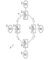
- FIG. 1 shows an example of an optical ring network system 100 according to an embodiment.
- the optical transmission device 101-A, the optical transmission device 101-B, the optical transmission device 101-C, and the optical transmission device 101-D are ring-shaped networks (optical ring network 102) composed of optical fibers. ) Is connected.
- the alphabet at the end of the reference numeral is omitted and the optical transmission device is omitted. It is described as 101.
- an alphabet is added to the end of the reference numeral and the description is made, for example, optical transmission device 101-A.
- An external NW 103 is connected to each optical transmission device 101, and communication between these external NW 103s is possible via the optical ring network 102.
- the external NW 103 is a NW connected to the above-mentioned optical ring network system, and a NW device or the like is connected to the external NW 103.
- the optical ring network system 100 uses the burst optical ring network technology.
- communication between the plurality of optical transmission devices 101 is performed on the optical ring network 102 by time-division multiplexing (optical TDMA (Time Division Multiple Access)) of optical signals.
- the optical ring network system 100 may be operated with one wavelength or may be operated with multiple wavelengths.
- the optical signal is time-division-multiplexed for each wavelength.
- one optical transmission device 101 is a parent device (corresponding to a parent communication device), and the other optical transmission device 101 is a child device (corresponding to a child communication device).
- the parent device in the initial state is predetermined. For example, when the optical transmission device 101-A is the parent device, the optical transmission device 101-B, the optical transmission device 101-C, and the optical transmission device 101-D are used. It becomes a child device.
- the optical transmission device 101 of the parent device determines the transmission timing of the optical signal of the optical transmission device 101 including its own device, and assigns an assigned signal for allocating the transmission timing of the optical signal to the optical transmission device 101 of the child device. Send. Further, the optical transmission device 101 of the parent device transmits a search signal for detecting whether or not the optical transmission device 101 of the child device is newly connected to the optical ring network 102.
- the assigned signal and the search signal correspond to the control signal transmitted by the parent device to the child device.
- the assigned signal has information for allocating the transmission timing of the optical signal.
- the assigned signal is a device identifier for distinguishing the optical transmission device 101 to be assigned, a transmission start time indicating the time when the optical signal is started to be transmitted, and a transmission time (transmission duration) indicating the time when the optical signal is being transmitted. ) And other information.
- the search signal is a transmission start time indicating the time when the newly connected optical transmission device 101 starts transmitting the registration request signal for requesting registration from the parent device, and a transmission indicating the time when the registration request signal is being transmitted. Includes information such as time.
- the optical transmission device 101 of the slave device transmits an optical signal at the transmission timing assigned by the assigned signal received from the parent device. Further, when the optical transmission device 101 of the child device is newly connected to the optical ring network 102, the optical transmission device 101 transmits a registration request signal to the parent device based on the search signal received from the parent device. As a result, the optical transmission device 101 of the child device newly connected to the optical ring network 102 can be registered in the parent device. Then, the optical transmission device 101 of the registered child device can transmit the optical signal at the transmission timing assigned by the assigned signal received from the parent device.
- the optical transmission device 101 that functions as the parent device is the timing at which all the optical transmission devices 101 including the own device transmit the optical signal and the unregistered optical transmission device 101 that is newly connected. Control registration etc.
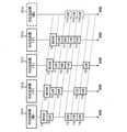
- FIG. 2 shows an example of communication of assigned signals in the case where the parent device is the optical transmission device 101-A, the child device is the optical transmission device 101-B, the optical transmission device 101-C, and the optical transmission device 101-D in FIG. Is shown.
- the optical transmission device 101 is a parent device, a (parent) is added, and if the optical transmission device 101 is a child device, a (child) is added to describe the optical transmission device 101 as the optical transmission device (parent) 101 and the optical transmission device (child) 101. ..
- the optical transmission device (parent) 101-A transmits an allocation signal (control signal) for assigning a transmission timing to each optical transmission device (child) 101 at time T1 (described as [allocation transmission]). Then, at time T2, the optical transmission device (child) 101-B receives the allocation signal (described as [assignment reception]). Similarly, at times T3 and T4, the optical transmission devices (children) 101-C and 101-D receive the assigned signals, respectively.
- the optical transmission device (parent) 101-A also assigns a timing for transmitting a data signal to its own device. In the example of FIG. 4, the transmission timings of the respective data signals of the optical transmission devices (parents) 101-A, 101-B, 101-C and 101-D are assigned as T5, T9, T13 and T16.
- the data signals transmitted from the optical transmission device (parent) 101-A at time T5 are received by the optical transmission devices (child) 101-B, 101-C, 101-D at times T6, T7, and T8, respectively.
- the data signals transmitted from the optical transmission device (child) 101-B at time T9 are the optical transmission devices (child) 101-C, 101-D and the optical transmission device (parent) 101 at T10, T11, and T12. -Received at A respectively.
- the data signals transmitted from the optical transmission device (child) 101-C at time T13 are the optical transmission device (child) 101-D, the optical transmission device (parent) 101-A, and optical at T14, T15, and T16. It is received by the transmission device (child) 101-B, respectively.
- the data signals transmitted from the optical transmission device (child) 101-D at time T17 are the optical transmission device (parent) 101-A and the optical transmission device (child) 101-B, 101 at T18, T19, and T20. -Received at C respectively.
- one of the plurality of optical transmission devices 101 connected to the optical ring network 102 operates as the parent device, and the parent device assigns the optical signal transmission timing to all the optical transmission devices 101. , Communication by time division multiplex becomes possible.
- FIG. 3 shows an example of communication of a search signal in the case where the parent device is the optical transmission device 101-A in FIG.
- transmission / reception of each signal is described in the same manner as in FIG.
- the optical transmission device (parent) 101-A provides a control signal (referred to as a search signal) for searching for an unregistered optical transmission device (child) 101-B newly connected to the optical ring network 102 at time T1.
- Send described as [Search Send]
- the optical transmission device (child) 101-B receives the search signal (described as [search reception]).
- the unregistered optical transmission device (child) 101-B that has received the search signal opticals a control signal (referred to as a registration request signal) for requesting registration at time T3 of the transmission start time described in the search signal. It is transmitted to the transmission device (parent) 101-A.
- the optical transmission device (parent) 101-A Upon receiving the registration request signal at time T4, the optical transmission device (parent) 101-A performs the registration process and notifies the optical transmission device (child) 101-B that the registration is completed. (T5) to transmit a control signal (registration notification signal) for the purpose.
- the optical transmission device (child) 101-B that received the registration notification signal at time T6 sets the optical transmission device (parent) 101-A at time T7 of the transmission start time described in the registration notification signal.
- a confirmation response signal indicating that the registration notification signal has been confirmed may be transmitted.
- the optical transmission device (parent) 101-A receives the confirmation response signal at time T8.
- one of the plurality of optical transmission devices 101 connected to the optical ring network 102 operates as the parent device, the parent device transmits a search signal, and the optical transmission device is newly connected. 101 can be registered.
- the optical transmission device 101 can continue the system operation by operating the optical transmission device 101 of the child device as a new parent device when the optical transmission device 101 of the parent device cannot operate normally. Has a function.
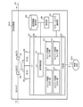
- FIG. 4 shows a configuration example of the optical transmission device 101-B that operates as a child device in FIG. 2.
- FIG. 4 shows a configuration example of the optical transmission device 101-B, but the optical transmission device 101-C and the optical transmission device 101-D operating as the same child device have the same configuration.
- the optical transmission device 101-A that operates as a parent device in FIG. 2 also has a function of operating as a child device.
- the four optical transmission devices 101 described with reference to FIG. 1 have the function of the parent device and the function of the child device, and one of them is selected to operate as the parent device or the child device.
- the optical transmission device 101 from which the function of the parent device is selected operates as the parent device
- the optical transmission device 101 from which the function of the child device is selected operates as the child device.
- the optical transmission device 101-B has a layer 1 processing unit (L1 unit) 201, a layer 2 processing unit (L2 unit) 202, a switch unit (SW unit) 203, and an optical transmission unit (B-Tx unit) 204. It has an optical receiving unit (B-Rx unit) 205, an optical coupler 206, an optical coupler 207, a signal information storage unit 208, a determination unit 209, and a master slave selection unit 210. Further, the L2 unit 202 has a signal detection unit 211, a timing control master unit 212, a network registration master unit 213, a timing control slave unit 312, and a network registration slave unit 313.
- the timing control master unit 212 and the network registration master unit 213 are functions of the parent device, and the timing control slave unit 312 and the network registration slave unit 313 are functions of the child device.
- the L1 unit 201 has a function of processing the first layer (physical layer) of the OSI reference model.
- the L2 unit 202 has a function of processing the second layer (data link layer) of the OSI reference model.
- the L2 unit 202 has a signal detection unit 211 described later, and the signal detection unit 211 detects an assigned signal or a search signal from an optical signal received from the optical ring network 102.
- the L2 unit 202 has a function of a parent device and a function of a child device, and operates by one of the functions based on a command of the master slave selection unit 210 described later.
- the transmission timing is controlled and the unregistered optical transmission device 101 is detected and registered.
- the transmission timing of the optical signal transmitted from the B-Tx unit 204 is controlled according to the transmission start time and the transmission time instructed by the parent device, and the search signal is received from the parent device and registered. ..
- the SW unit 203 is an electric packet switch such as an L2-SW connected to the external NW 103, and has a function of processing a packet transfer between the L2 unit 202 and the external NW 103 according to a preset rule.
- the B-Tx unit 204 is a transmission unit that intermittently outputs an optical signal, and transmits the signal transferred from the L1 unit 201 as an optical signal to the optical fiber via an optical coupler in a burst manner.
- the B-Rx unit 205 is a receiving unit that receives an intermittent optical signal, receives an optical signal in a burst from an optical fiber via an optical coupler, and transfers the signal to the L1 unit 201.
- the B-Tx unit 204 and the B-Rx unit 205 correspond to the communication unit.
- the optical coupler 206 and the optical coupler 207 have a function of branching the power of the input optical signal.
- the signal information storage unit 208 is composed of a storage medium such as a semiconductor memory.
- the signal information storage unit 208 stores the information described in the allocation signal and the search signal received from the parent device in a list format (referred to as a band information list) for each item, which will be described later.
- the determination unit 209 can sort items by item. For example, when the item of the band information list of the assigned signal is "device identifier / transmission start time / transmission time", the list can be rearranged in descending order by the transmission start time.
- the assigned signal stores information for notifying the optical transmission device 101 of all the child devices connected to the optical ring network 102 of the transmission timing. As a result, each child device can know the "device identifier, transmission start time, transmission time" of the other child device.
- the determination unit 209 receives a notification of the reception status of the assigned signal or the search signal from the signal detection unit 211 of the L2 unit 202, and determines the state of the parent device. For example, the determination unit 209 determines that the parent device cannot operate normally due to a failure or the like when the allocation signal or the search signal is not received within a predetermined period. Then, when the determination unit 209 determines that the parent device cannot operate normally due to a failure or the like, the determination unit 209 determines whether or not the own device should operate as the parent device. For example, the determination unit 209 determines whether or not the own device should operate as a new parent device based on the band information list of the assigned signal stored in the signal information storage unit 208.
- the determination unit 209 instructs the master slave selection unit 210 whether the own device operates as a parent device or the own device operates as a child device.
- the determination as to whether or not the own device should operate as the parent device is performed in parallel in the optical transmission device 101 of all the child devices connected to the optical ring network 102.
- the plurality of child devices are processed so as not to operate as the parent device. This process will be described in the flowchart described later.
- the master / slave selection unit 210 exclusively controls whether the optical transmission device 101 functions as a parent device or a child device based on the instruction of the determination unit 209.
- the master slave selection unit 210 operates the timing control master unit 212 and the network registration master unit 213 of the L2 unit 202.
- the master slave selection unit 210 operates the timing control slave unit 312 and the network registration slave unit 313 of the L2 unit 202.
- the signal detection unit 211 detects the assigned signal or the search signal from the optical signal received from the optical ring network 102. Then, the signal detection unit 211 stores the information regarding the detected allocation signal or search signal in the signal information storage unit 208, and notifies the determination unit 209 of the reception status.
- the information regarding the allocation signal or the search signal is information such as the device identifier, the transmission start time, and the transmission time.
- the reception status is information such as whether or not the assigned signal or the search signal is received and the reception time.
- the timing control master unit 212 operates when the master / slave selection unit 210 makes the own device function as a parent device.
- the timing control master unit 212 determines the transmission timing of the all-optical transmission device 101 connected to the optical ring network 102 including the own device, and determines the transmission timing of the optical signal to the own device (or a child device). It has a function to indicate the transmission time.
- the timing control master unit 212 controls the transmission timing of the optical signal transmitted from the B-Tx unit 204.
- the instruction of the transmission timing to the optical transmission device 101 other than the own device is performed by communication of each unit of the L1 unit 201, the L2 unit 202, the B-Tx unit 204, and the B-Rx unit 205.
- the network registration master unit 213 operates when the master / slave selection unit 210 makes the own device function as a parent device.
- the network registration master unit 213 initially communicates with the unregistered optical transmission device 101 in order to detect the connection of the unregistered optical transmission device 101 to the optical ring network 102 and register the unregistered optical transmission device 101 with the optical ring network system 100. Perform the connection sequence.
- the network registration master unit 213 transmits a search signal in order to search for a newly connected unregistered optical transmission device 101.
- the network registration master unit 213 when the network registration master unit 213 receives the registration request signal from the unregistered optical transmission device 101 that responds to the search signal, the network registration master unit 213 performs registration processing as a connection device to the optical ring network 102, and does not receive the registration notification signal. It is transmitted to the registered optical transmission device 101.
- the timing control slave unit 312 operates when the master slave selection unit 210 causes the own device to function as a child device.
- the timing control slave unit 312 controls the transmission timing of the optical signal transmitted from the B-Tx unit 204 according to the transmission start time and the transmission time instructed by the parent device.
- the network registration slave unit 313 operates when the master / slave selection unit 210 makes the own device function as a child device. As described with reference to FIG. 3, the network registration slave unit 313 transmits a registration request signal to the parent device when the search signal is received from the parent device, and the registration is transmitted from the parent device that has received the registration request signal. Receive a notification signal.
- the optical transmission device 101 can operate as a parent device or a child device. Then, when the own device is a child device, it is determined whether or not the parent device is operating normally based on the reception status of the assigned signal or the search signal transmitted from the parent device. If it is determined that the parent device cannot operate normally due to a failure or the like, the own device or another child device operates as the parent device, which enables redundancy of the optical ring network system 100 and continues system operation. Can be done.
- band information list Next, the band information list will be described. For example, when the item of the band information list obtained by the assigned signal is "device identifier / transmission start time / transmission time", the following band information list is stored in the signal information storage unit 208.
- the band information list can be sorted by item by the determination unit 209. s (s: integer) indicates the order of the list. Since the allocation signal stores information on the "device identifier, transmission start time, and transmission time" of all the devices to be assigned, each child device can know the information of the other child devices.
- the transmission start time and transmission time are specified, for example, in nanosecond units.
- the determination unit 209 determines whether or not the own device should operate as a new parent device based on the list sorted in this way. For example, by predetermining that the child device having the device identifier with the earliest transmission start time operates as a new parent device, the determination unit 209 selects one new parent device from among the plurality of child devices. You can choose.
- FIG. 5 shows an example of the switching process to the parent device.
- FIG. 5 is a process when the optical transmission device 101 is operating as a child device, for example, the signal information storage unit 208, the determination unit 209, and the master unit of the optical transmission device 101-B described with reference to FIG. It is executed by the slave selection unit 210 and the signal detection unit 211.
- the program corresponding to the process described with reference to FIG. 5 may be executed by a computer or an integrated circuit such as an FPGA (Field Programmable Gate Array). Further, the program may be recorded on a storage medium and provided, or may be provided through a network.
- FPGA Field Programmable Gate Array
- step S101 the optical transmission device 101 operating as a child device starts a process of determining whether or not the parent device is operating normally.
- step S102 the determination unit 209 initializes the counter i and the counter s to 0.
- step S103 the determination unit 209 waits for processing for a preset time t.
- the time t is set to a value larger than the time interval at which the parent device transmits the allocation signal or the search signal.
- step S104 the determination unit 209 confirms whether or not the assigned signal or the search signal has been received from the parent device by the signal detection unit 211, and if so, returns to the process of step S102 and performs the same. Repeat the process. If not received (N), the process proceeds to step S105.
- the signal detection unit 211 stores the received information regarding the assigned signal or the search signal in the signal information storage unit 208, and creates a band information list.
- step S105 the determination unit 209 increments the counter i by one and proceeds to the process of step S106.
- step S106 the determination unit 209 determines whether or not the counter i has reached the preset threshold value k (k is an integer).
- k k (Y)
- the process proceeds to step S107, and when i ⁇ k (N), the process returns to step S103 and the same process is repeated.
- it is determined whether or not the allocation signal or the search signal is received in a predetermined period (t ⁇ k period in the example of FIG. 5).
- the determination unit 209 determines that the parent device cannot transmit the assigned signal or the search signal due to a failure or the like, and whether or not the own device should operate as the parent device. Starts the process of determining.
- step S107 the determination unit 209 sorts according to a predetermined condition with reference to the band information list stored in the signal information storage unit 208, and determines whether or not the own device meets the condition. do.
- the band information list is sorted in order from the earliest transmission start time, and it is determined whether or not the sth device identifier is the identifier of the own device. Then, when the s-th device identifier is the identifier of the own device (Y), the process proceeds to the process of step S111, and when the s-th device identifier is not the identifier of the own device (N), the process proceeds to the process of step S108. ..
- the process proceeds to step S111, and the own device operates as the parent device. Start.
- step S108 the determination unit 209 waits for processing for a preset time t1.
- the time t1 is set to a value larger than the time required for another child device to start operating as a parent device.
- step S109 the determination unit 209 confirms whether or not the assigned signal or the search signal has been received from the new parent device by the signal detection unit 211, and if so, returns to the process of step S102. The same process is repeated. If not received (N), the process proceeds to step S110.
- step S110 the determination unit 209 increments the counter s by one and returns to the process of step S107.
- step S110 the determination unit 209 increments the counter s by one and returns to the process of step S107.
- step S111 since the own device is selected as the new parent device, the determination unit 209 instructs the master slave selection unit 210 to start the operation as the parent device.
- step S112 the optical transmission device 101 operating as a child device starts operating as a parent device and ends the process of FIG.
- the optical transmission device 101 when the own device is a child device, is the parent device operating normally based on the reception status of the assigned signal or the search signal transmitted from the parent device? Judge whether or not. Then, when it is determined that the parent device cannot operate normally due to a failure or the like, any of the optical transmission devices 101 operating as the child device starts the operation as the parent device. This makes it possible to make the optical ring network system 100 redundant, and even if the parent device fails, the system operation is continued.
- FIG. 6 shows a comparative example optical ring network system 800.
- one optical transmission device (parent) 801-A and one or more optical transmission devices (child) 801-B to 801-D are connected by an optical ring network 102.
- External NW103-A, 103-B, 103-C and 103-D are connected to the optical transmission device (parent) 801-A and the optical transmission devices (child) 801-B to 801-D, respectively. ..
- an optical transmission device 801 that operates as a parent device is predetermined.
- the optical transmission device 801-A is set as a parent device, and the optical transmission devices 801-B, 801-C and 801-D are set as child devices by a maintenance person or the like.
- the timing and new timing at which the optical transmission device (parent) 801-A transmits the optical signals of the optical transmission device (child) 801-B, the optical transmission device (child) 801-C, and the optical transmission device (child) 801-D Controls registration and so on.
- the optical transmission device (parent) 801-A cannot operate normally due to a failure or the like, the timing of transmitting the optical signal and the control of new registration are not performed, and the system operation cannot be continued.
- the maintenance person repairs the optical transmission device (parent) 801-A, or the optical transmission device (child) 801-B, the optical transmission device (child) 801-C, and the optical transmission device (child) 801-D. Either one needs to be reconfigured to operate as the parent device.
- FIG. 7 shows a configuration example of the optical transmission device (parent) 801-A and the optical transmission device (child) 801-B shown in FIG.
- the optical transmission device (child) 801-C and the optical transmission device (child) 801-D have the same configuration as the optical transmission device (child) 801-B.
- FIG. 7 the blocks having the same name other than the L2 part 902-A of the optical transmission device (parent) 801-A and the L2 part 902-B of the optical transmission device (child) 801-B are shown in FIG. Since the operation is the same as that of the optical transmission device 101-A according to the embodiment, duplicate description will be omitted.
- Sections 901-B, SW section 903-B, B-Tx section 904-B, B-Rx section 905-B, optical coupler 906-B, and optical coupler 907-B are optical transmissions according to the embodiment shown in FIG. It operates in the same manner as the L1 unit 201-A, SW unit 203-A, B-Tx unit 204-A, B-Rx unit 205-A, optical coupler 206-A, and optical coupler 207-A of the apparatus 101-A.
- the optical transmission device (parent) 801-A is preset in the parent device
- the optical transmission device (child) 801-B is preset in the child device.
- the optical transmission device 101 according to the embodiment of FIG. 4 has a function of detecting a failure of the parent device and switching the child device to the parent device.
- the L2 unit 902-A of the optical transmission device (parent) 801-A set as the parent device has a timing control master unit 912 and a network registration master unit 913.
- the timing control master unit 912 determines the transmission timing of the all-optical transmission device 801 connected to the optical ring network 102 including the own device, similarly to the timing control master unit 212 of the embodiment shown in FIG. Then, the timing control master unit 912 instructs the own device (or the child device) the time at which the optical signal is transmitted and the time at which the optical signal is transmitted.
- the network registration master unit 913 detects the connection of the unregistered optical transmission device (child) 801 to the optical ring network 102 and connects to the optical ring network system 800. Register.
- the optical transmission device (parent) 801-A of the comparative example is preset so as to function as the parent device.
- the optical transmission device (child) 801-B set as a child device has a timing control slave unit 922 and a network registration slave unit 923 in the L2 unit 902-B.
- the timing control slave unit 922 has the transmission timing of the optical signal transmitted from the B-Tx unit 904 according to the transmission start time and the transmission time instructed by the parent device. To control.
- the network registration slave unit 923 transmits a registration request signal to the parent device and receives the registration request signal when the search signal is received from the parent device. Receives the registration notification signal transmitted from the master device.
- the optical transmission device 801 of the comparative example is preset as a parent device or a child device.
- the optical transmission device (parent) 801-A is set as the parent device, and the devices other than the optical transmission device (parent) 801-A are the child devices.
- the optical transmission device (parent) 801-A cannot operate normally due to a failure or the like, the timing of transmitting the optical signal and the control of new registration are not performed, and there arises a problem that the system operation cannot be continued.
- the optical transmission device 101 has the functions of both the master device and the child device, and the function of selecting one of them to operate as the parent device or the child device. ..
- the optical transmission device 101 when the function of the master device is selected, the optical transmission device 101 operates as a master device, and when the function of the child device is selected, the optical transmission device 101 operates as a child device.
- the optical transmission device 101 according to the embodiment confirms the state of the parent device when operating as the child device, and if the parent device cannot operate normally due to a failure or the like, one of the child devices automatically operates. Since it switches to the parent device, the system operation can be continued.
- the communication device, communication method, communication system, and communication program according to the present invention are parents that control a plurality of optical transmission devices connected to an optical ring network that communicates by time-dividing multiplexing optical signals.
- the child device operates as a new parent device, so that the system operation can be continued.
- 100, 800 ... Optical ring network system 101,801 ... Optical transmission device; 102 ... Optical ring network; 103 ... External NW; 201,901 ... L1 part; 202,902 ... L2 part; 203,903 ... SW part; 204,904 ... B-Tx part; 205,905 ... B-Rx part; 206,207,906,907 ... Optical coupler; 212, 912 ... Timing control master section; 213,913 ... Network registration master section; 312,922 ... Timing control slave section; 313,923 ... Network registration slave section
Landscapes
- Engineering & Computer Science (AREA)
- Computer Networks & Wireless Communication (AREA)
- Signal Processing (AREA)
- Physics & Mathematics (AREA)
- Electromagnetism (AREA)
- Computing Systems (AREA)
- Small-Scale Networks (AREA)
- Optical Communication System (AREA)
Abstract
光リングネットワークに接続され、光信号を時分割多重により通信を行うとともに、光信号の送信タイミングを制御するための制御信号を親の通信装置から受信する通信部と、制御信号が予め決められた期間に受信されない場合に、親の通信装置が正常に動作していないと判断し、自装置を新たな親の通信装置として動作させる判定部とを有する。これにより、親装置が正常に動作できない場合でも、子装置が親装置として動作するので、システム運用が継続可能である。
Description
本発明は、通信システムを構成する光リングネットワークにおいて、光信号を時分割多重して通信を行う技術に関する。
従来の光リングネットワークシステムは、光リングネットワークに接続される複数の光伝送装置のそれぞれに予め割り当てられた波長の光信号をOADM(Optical add-drop multiplexer)技術により多重して通信を行っている(例えば非特許文献1参照)。
一方、OADMではなく、時分割多重により光信号を伝送するバースト光リングネットワーク技術が知られている。この技術では、光リングネットワークに接続される複数の光伝送装置のうち、1台の光伝送装置が親装置、他の光伝送装置が子装置、としてそれぞれ動作する。親装置は、割当信号と探索信号を送信することにより、自装置を含む子装置のデータ送信タイミングの制御と新たに光リングネットワークに接続される子装置の登録とを行う。このようにして、光リングネットワークに接続される複数の光伝送装置は、バースト光リングネットワーク技術により、光信号を時分割多重して通信することができる。
坂巻他,"より柔軟な光ノードを実現する光スイッチ技術,"NTT技術ジャーナル,2013.11.(https://www.ntt.co.jp/journal/1311/files/jn201311016.pdf)
ところが、バースト光リングネットワーク技術において、親装置が故障などで正常に動作できない場合、データ送信タイミングなどの制御が行われないため、システム運用の継続が難しいという問題がある。
本発明は、光信号を時分割多重して通信する光リングネットワークに接続される複数の光伝送装置を制御する親装置が正常に動作できない場合に、子装置が新たな親装置として動作することにより、システム運用を継続できる通信装置、通信方法、通信システムおよび通信プログラムを提供することを目的とする。
本発明の通信装置は、光リングネットワークに接続され、光信号を時分割多重により通信を行うとともに、光信号の送信タイミングを制御するための制御信号を親の通信装置から受信する通信部と、前記制御信号が予め決められた期間に受信されない場合に、前記親の通信装置が正常に動作していないと判断し、自装置を新たな親の通信装置として動作させる判定部とを有することを特徴とする。
また、本発明は、複数の通信装置のうち、1台を親の通信装置、その他を子の通信装置として光リングネットワークで接続される通信システムで用いる通信方法であって、前記親の通信装置は、複数の前記子の通信装置に光信号を時分割多重により送信するときの送信タイミングを制御するための制御信号を送信し、前記子の通信装置は、前記親の通信装置から受信する前記制御信号の送信タイミングに基づいて、光信号を前記光リングネットワークに送信するとともに、前記制御信号が予め決められた期間に受信されない場合に、前記親の通信装置が正常に動作していないと判断し、自装置が新たな親の通信装置として動作することを特徴とする。
また、本発明は、複数の通信装置のうち、1台を親の通信装置、その他を子の通信装置として光リングネットワークで接続される通信システムにおいて、前記親の通信装置は、複数の前記子の通信装置に光信号を時分割多重により送信するときの送信タイミングを制御するための制御信号を送信し、前記子の通信装置は、前記親の通信装置から受信する前記制御信号の送信タイミングに基づいて、光信号を前記光リングネットワークに送信するとともに、前記制御信号が予め決められた期間に受信されない場合に、前記親の通信装置が正常に動作していないと判断し、自装置が新たな親の通信装置として動作することを特徴とする。
また、本発明の通信プログラムは、前記通信装置の前記判定部が行う処理をコンピュータもしくは集積回路に実行させることを特徴とする。
本発明に係る通信装置、通信方法、通信システムおよび通信プログラムは、光信号を時分割多重して通信する光リングネットワークに接続される複数の光伝送装置を制御する親装置が正常に動作できない場合に、子装置が新たな親装置として動作することにより、システム運用を継続することができる。
以下、図面を参照して本発明に係る通信装置、通信方法、通信システムおよび通信プログラムの実施形態について説明する。なお、以降で説明する実施形態では、複数の光伝送装置(通信装置に対応)が光リングネットワークで接続される光リングネットワークシステム(通信システムに対応)について説明する。
図1は、実施形態に係る光リングネットワークシステム100の一例を示す。
図1の例では、光伝送装置101-A、光伝送装置101-B、光伝送装置101-Cおよび光伝送装置101-Dが、光ファイバで構成されるリング型のネットワーク(光リングネットワーク102)で接続されている。
ここで、光伝送装置101-A、光伝送装置101-B、光伝送装置101-Cおよび光伝送装置101-Dに共通する説明を行う場合は、符号末尾のアルファベットを省略して光伝送装置101と記載する。複数の光伝送装置101のうち、特定の装置を指す場合は、符号末尾にアルファベットを付加して、例えば光伝送装置101-Aと記載する。外部NW(NetWork)103-A、外部NW103-B、外部NW103-Cおよび外部NW103-Dについても同様に記載する。
各光伝送装置101には、外部NW103がそれぞれ接続され、光リングネットワーク102を介して、これらの外部NW103間での通信が可能である。
外部NW103は、上述の光リングネットワークシステムに接続されるNWであり、NW装置などが接続される。
ここで、実施形態に係る光リングネットワークシステム100は、バースト光リングネットワーク技術を用いる。これにより、複数の光伝送装置101間の通信は、光信号を時分割多重(光TDMA(Time Division Multiple Access))して、光リングネットワーク102上で実施される。なお、光リングネットワークシステム100は、1つの波長で運用されてもよいし、波長多重して運用されてもよい。波長多重の場合は、波長ごとに光信号が時分割多重される。
図1において、複数の光伝送装置101のうち、1台の光伝送装置101が親装置(親の通信装置に対応)、他の光伝送装置101が子装置(子の通信装置に対応)として動作する。ここで、初期状態における親装置は予め決められており、例えば光伝送装置101-Aが親装置である場合、光伝送装置101-B、光伝送装置101-Cおよび光伝送装置101-Dは子装置となる。
親装置の光伝送装置101は、自装置を含む光伝送装置101の光信号の送信タイミングを決定し、子装置の光伝送装置101に対して、光信号の送信タイミングを割り当てるための割当信号を送信する。また、親装置の光伝送装置101は、子装置の光伝送装置101が新たに光リングネットワーク102に接続されたか否かを検出するための探索信号を送信する。なお、割当信号および探索信号は、親装置が子装置に送信する制御信号に対応する。
ここで、割当信号は、光信号の送信タイミングを割り当てるための情報を有する。例えば割当信号は、割り当て対象の光伝送装置101を区別するための装置識別子、光信号の送信を開始する時刻を示す送信開始時刻、光信号を送信している時間を示す送信時間(送信継続時間)などの情報を含む。探索信号は、新たに接続された光伝送装置101が親装置に登録を要求するための登録要求信号の送信を開始する時刻を示す送信開始時刻、登録要求信号を送信している時間を示す送信時間などの情報を含む。
子装置の光伝送装置101は、親装置から受信する割当信号により割り当てられた送信タイミングで光信号を送信する。また、子装置の光伝送装置101は、新たに光リングネットワーク102に接続する場合、親装置から受信する探索信号に基づいて、登録要求信号を親装置に送信する。これにより、新たに光リングネットワーク102に接続された子装置の光伝送装置101は、親装置に登録することができる。そして、登録された子装置の光伝送装置101は、親装置から受信する割当信号により割り当てられた送信タイミングで光信号を送信することができる。
このように、実施形態では、親装置として機能する光伝送装置101は、自装置を含む全ての光伝送装置101が光信号を送信するタイミングおよび新規に接続される未登録の光伝送装置101の登録などを制御する。
(割当信号について)
図2は、図1において、親装置が光伝送装置101-A、子装置が光伝送装置101-B、光伝送装置101-Cおよび光伝送装置101-Dである場合の割当信号の通信例を示す。ここで、光伝送装置101が親装置の場合は(親)、子装置の場合は(子)を付加して、光伝送装置(親)101および光伝送装置(子)101のように記載する。
図2は、図1において、親装置が光伝送装置101-A、子装置が光伝送装置101-B、光伝送装置101-Cおよび光伝送装置101-Dである場合の割当信号の通信例を示す。ここで、光伝送装置101が親装置の場合は(親)、子装置の場合は(子)を付加して、光伝送装置(親)101および光伝送装置(子)101のように記載する。
光伝送装置(親)101-Aは、時刻T1に送信タイミングを各光伝送装置(子)101に割り当てるための割当信号(制御信号)を送信する([割当送]と記載)。そして、時刻T2に光伝送装置(子)101-Bが割当信号を受信する([割当受]と記載)。同様に、時刻T3およびT4にそれぞれ光伝送装置(子)101-Cおよび101-Dが割当信号を受信する。なお、光伝送装置(親)101-Aは、自装置に対してもデータ信号を送信するタイミングを割り当てる。図4の例では、光伝送装置(親)101-A、101-B、101-Cおよび101-Dのそれぞれのデータ信号の送信タイミングが、T5、T9、T13およびT16のように割り当てられる。
そして、時刻T5に光伝送装置(親)101-Aから送信されたデータ信号は、時刻T6、T7、T8に光伝送装置(子)101-B、101-C、101-Dでそれぞれ受信される。ここで、上述の動作をT5[A送]->T6[A受]->T7[A受]->T8[A受]と記載する。同様に、時刻T9に光伝送装置(子)101-Bから送信されたデータ信号は、T10、T11、T12に光伝送装置(子)101-C、101-D、光伝送装置(親)101-Aでそれぞれ受信される。同様に、時刻T13に光伝送装置(子)101-Cから送信されたデータ信号は、T14、T15、T16に光伝送装置(子)101-D、光伝送装置(親)101-A、光伝送装置(子)101-Bでそれぞれ受信される。同様に、時刻T17に光伝送装置(子)101-Dから送信されたデータ信号は、T18、T19、T20に光伝送装置(親)101-A、光伝送装置(子)101-B、101-Cでそれぞれ受信される。
このように、光リングネットワーク102に接続される複数の光伝送装置101のうち、いずれか1台が親装置として動作し、親装置が全ての光伝送装置101に光信号の送信タイミングを割り当てるので、時分割多重による通信が可能になる。
(探索信号について)
図3は、図1において、親装置が光伝送装置101-Aである場合の探索信号の通信例を示す。なお、図3において、各信号の送受信は、図2と同様に記載する。
図3は、図1において、親装置が光伝送装置101-Aである場合の探索信号の通信例を示す。なお、図3において、各信号の送受信は、図2と同様に記載する。
光伝送装置(親)101-Aは、時刻T1に光リングネットワーク102に新たに接続される未登録の光伝送装置(子)101-Bを探索するための制御信号(探索信号と称する)を送信する([探索送]と記載)。そして、時刻T2に光伝送装置(子)101-Bが探索信号を受信する([探索受]と記載)。探索信号を受信した未登録の光伝送装置(子)101-Bは、探索信号に記載された送信開始時刻の時刻T3に、登録を要求するための制御信号(登録要求信号と称する)を光伝送装置(親)101-Aに送信する。時刻T4に登録要求信号を受信した光伝送装置(親)101-Aは、登録処理を行うとともに、登録が完了したことを光伝送装置(子)101-Bに伝えるために、登録を通知するための制御信号(登録通知信号)を送信する(T5)。なお、時刻T6に登録通知信号を受信した光伝送装置(子)101-Bは、光伝送装置(親)101-Aに対して、登録通知信号に記載された送信開始時刻の時刻T7に、登録通知信号を確認したことを示す確認応答信号を送信するようにしてもよい。この場合、光伝送装置(親)101-Aは、時刻T8に確認応答信号を受信する。
このように、光リングネットワーク102に接続される複数の光伝送装置101のうち、いずれか1台が親装置として動作し、親装置が探索信号を送信して、新たに接続される光伝送装置101を登録することができる。
ここで、図1に示す光リングネットワークシステム100において、親装置が故障等で正常に動作できない場合、割当信号および探索信号の送信が行われないため、システム運用が継続できないという問題が生じる。そこで、実施形態に係る光伝送装置101は、親装置の光伝送装置101が正常に動作できない場合に、子装置の光伝送装置101が新たな親装置として動作することにより、システム運用を継続できる機能を有する。
(光伝送装置101の構成例)
図4は、図2で子装置として動作する光伝送装置101-Bの構成例を示す。ここで、図4では、光伝送装置101-Bの構成例を示すが、同じ子装置として動作する光伝送装置101-Cおよび光伝送装置101-Dについても同様の構成である。なお、図2で親装置として動作する光伝送装置101-Aも子装置として動作する機能を有する。
図4は、図2で子装置として動作する光伝送装置101-Bの構成例を示す。ここで、図4では、光伝送装置101-Bの構成例を示すが、同じ子装置として動作する光伝送装置101-Cおよび光伝送装置101-Dについても同様の構成である。なお、図2で親装置として動作する光伝送装置101-Aも子装置として動作する機能を有する。
このように、図1で説明した4つの光伝送装置101は、親装置の機能と子装置の機能とを有し、いずれか一方を選択して親装置または子装置として動作する。例えば親装置の機能が選択された光伝送装置101は親装置として動作し、子装置の機能が選択された光伝送装置101は子装置として動作する。
図4において、光伝送装置101-Bは、レイヤ1処理部(L1部)201、レイヤ2処理部(L2部)202、スイッチ部(SW部)203、光送信部(B-Tx部)204、光受信部(B-Rx部)205、光カプラ206、光カプラ207、信号情報保存部208、判定部209およびマスター・スレイブ選択部210を有する。また、L2部202は、信号検知部211、タイミング制御マスター部212、ネットワーク登録マスター部213、タイミング制御スレイブ部312およびネットワーク登録スレイブ部313を有する。ここで、タイミング制御マスター部212およびネットワーク登録マスター部213は親装置の機能、タイミング制御スレイブ部312およびネットワーク登録スレイブ部313は子装置の機能である。
L1部201は、OSI参照モデル第1層(物理層)を処理する機能を有する。
L2部202は、OSI参照モデル第2層(データリンク層)を処理する機能を有する。実施形態では、L2部202は、後述の信号検知部211を有し、信号検知部211は、光リングネットワーク102から受信する光信号から割当信号または探索信号を検知する。また、L2部202は、親装置の機能と子装置の機能とを有し、後述のマスター・スレイブ選択部210の指令に基づいて、いずれかの機能で動作する。親装置の場合は、送信タイミングの制御および未登録の光伝送装置101の検知・登録を行う。子装置の場合は、親装置から指示された送信開始時刻および送信時間に従い、B-Tx部204から送信する光信号の送信タイミングを制御するとともに、親装置から探索信号を受信して登録を行う。
SW部203は、外部NW103に接続されるL2-SWなどの電気パケットスイッチであり、予め設定されたルールに従い、L2部202と外部NW103との間のパケット転送を処理する機能を有する。
B-Tx部204は、光信号を断続的に出力する送信部で、光カプラを介して光ファイバに対して、L1部201から転送された信号を光信号としてバースト的に送信する。
B-Rx部205は、断続的な光信号を受信する受信部で、光カプラを介して、光ファイバから光信号をバースト的に受信し、L1部201に信号を転送する。ここで、B-Tx部204およびB-Rx部205は、通信部に対応する。
光カプラ206および光カプラ207は、入力される光信号のパワーを分岐する機能を有する。
信号情報保存部208は、半導体メモリなどの記憶媒体で構成される。自装置が子装置の場合、信号情報保存部208には、親装置から受信する割当信号や探索信号に記載されている情報が項目別にリスト形式(帯域情報リストと称する)で保存され、後述の判定部209により項目ごとに並べ替えが可能である。例えば割当信号の帯域情報リストの項目が「装置識別子・送信開始時刻・送信時間」である場合、送信開始時刻で降順にリストの並び替えが可能である。なお、図2で説明したように、割当信号には、光リングネットワーク102に接続される全ての子装置の光伝送装置101に送信タイミングを通知するための情報が格納されている。これにより、各子装置は、他の子装置の「装置識別子・送信開始時刻・送信時間」を知ることができる。
判定部209は、L2部202の信号検知部211から割当信号または探索信号の受信状況の通知を受け、親装置の状態を判定する。例えば、判定部209は、予め決められた期間に割当信号または探索信号が受信されない場合に、親装置が故障等で正常に動作できないと判定する。そして、判定部209は、親装置が故障等で正常に動作できないと判定した場合、自装置が親装置として動作すべきか否かを判断する。例えば、判定部209は、信号情報保存部208に保存されている割当信号の帯域情報リストに基づいて、自装置が新たな親装置として動作すべきか否かを判断する。なお、帯域情報リストによる自装置が新たな親装置として動作すべきか否かを判断方法については、後述する。そして、判定部209は、自装置が親装置として動作するか、自装置が子装置として動作するかをマスター・スレイブ選択部210に指示する。ここで、自装置が親装置として動作すべきか否かを判断は、光リングネットワーク102に接続される全ての子装置の光伝送装置101において、並行して行われている。なお、実施形態では、複数の子装置が親装置として動作しないように処理される。この処理については、後述のフローチャートで説明する。
マスター・スレイブ選択部210は、判定部209の指示に基づいて、光伝送装置101が親装置または子装置のどちらで機能するかを排他的に制御する。光伝送装置101が親装置として機能する場合、マスター・スレイブ選択部210は、L2部202のタイミング制御マスター部212およびネットワーク登録マスター部213を動作させる。逆に、光伝送装置101が子装置として機能する場合、マスター・スレイブ選択部210は、L2部202のタイミング制御スレイブ部312およびネットワーク登録スレイブ部313を動作させる。
信号検知部211は、光リングネットワーク102から受信する光信号から割当信号または探索信号を検知する。そして、信号検知部211は、検知した割当信号または探索信号に関する情報を信号情報保存部208に保存するとともに、受信状況を判定部209に通知する。ここで、割当信号または探索信号に関する情報は、装置識別子、送信開始時刻、送信時間などの情報である。また、受信状況は、例えば、割当信号または探索信号の受信の有無や受信時刻などの情報である。
タイミング制御マスター部212は、マスター・スレイブ選択部210が自装置を親装置として機能させる場合に動作する。タイミング制御マスター部212は、自装置を含む光リングネットワーク102に接続されている全光伝送装置101の送信タイミングを決定し、自装置(または子装置)に対して、光信号を送信する時刻と送信する時間を指示する機能を有する。なお、自装置の場合は、タイミング制御マスター部212がB-Tx部204から送信する光信号の送信タイミングを制御する。自装置以外の光伝送装置101への送信タイミングの指示は、L1部201、L2部202、B-Tx部204およびB-Rx部205の各部の通信により実施される。
ネットワーク登録マスター部213は、マスター・スレイブ選択部210が自装置を親装置として機能させる場合に動作する。ネットワーク登録マスター部213は、未登録の光伝送装置101の光リングネットワーク102への接続の検知および光リングネットワークシステム100への登録を行うために、未登録の光伝送装置101との間で初期接続シーケンスを実施する。具体的には、ネットワーク登録マスター部213は、新規に接続される未登録の光伝送装置101を探索するために探索信号を送信する。そして、ネットワーク登録マスター部213は、探索信号に応答した未登録の光伝送装置101から登録要求信号を受信した際に、光リングネットワーク102への接続装置として登録処理を行い、登録通知信号を未登録の光伝送装置101に送信する。
タイミング制御スレイブ部312は、マスター・スレイブ選択部210が自装置を子装置として機能させる場合に動作する。タイミング制御スレイブ部312は、親装置から指示された送信開始時刻および送信時間に従い、B-Tx部204から送信する光信号の送信タイミングを制御する。
ネットワーク登録スレイブ部313は、マスター・スレイブ選択部210が自装置を子装置として機能させる場合に動作する。ネットワーク登録スレイブ部313は、図3で説明したように、親装置から探索信号を受信した場合、親装置に対して登録要求信号を送信し、登録要求信号を受信した親装置から送信される登録通知信号を受信する。
このように、実施形態に係る光伝送装置101は、親装置または子装置として動作することができる。そして、自装置が子装置の場合に、親装置から送信される割当信号または探索信号の受信状況に基づいて、親装置が正常に動作しているか否かを判断する。親装置が故障等で正常に動作できないと判定した場合、自装置または他の子装置が親装置として動作することにより、光リングネットワークシステム100の冗長化が可能になり、システム運用を継続することができる。
(帯域情報リスト)
次に、帯域情報リストについて説明する。例えば割当信号により得られる帯域情報リストの項目が「装置識別子・送信開始時刻・送信時間」である場合、下記のような帯域情報リストが信号情報保存部208に保存される。ここで、帯域情報リストは、判定部209により項目ごとに並べ替えが可能である。s(s:整数)はリストの順番を示す。なお、割当信号には、割り当て対象の全装置の「装置識別子・送信開始時刻・送信時間」の情報が格納されているので、各子装置は、他の子装置の情報を知ることができる。
次に、帯域情報リストについて説明する。例えば割当信号により得られる帯域情報リストの項目が「装置識別子・送信開始時刻・送信時間」である場合、下記のような帯域情報リストが信号情報保存部208に保存される。ここで、帯域情報リストは、判定部209により項目ごとに並べ替えが可能である。s(s:整数)はリストの順番を示す。なお、割当信号には、割り当て対象の全装置の「装置識別子・送信開始時刻・送信時間」の情報が格納されているので、各子装置は、他の子装置の情報を知ることができる。
(帯域情報リストの一例)
s 装置識別子 送信開始時刻 送信時間
0 AAA TA 10
1 BBB TB 5
2 CCC TC 10
3 … … …
s 装置識別子 送信開始時刻 送信時間
0 AAA TA 10
1 BBB TB 5
2 CCC TC 10
3 … … …
上記の帯域情報リストは、送信開始時刻で降順に並び替えられている。例えばTA<TB<TCの順に並べ替えられており、送信開始時刻が一番早いs=0のリストは、装置識別子がAAA、送信開始時刻がTA、送信時間が10である。s=1のリストは、装置識別子がBBB、送信開始時刻がTB、送信時間が5、s=2のリストは、装置識別子がCCC、送信開始時刻がTC、送信時間が10である。なお、送信開始時刻および送信時間は、例えばナノ秒単位で指示される。判定部209は、このようにして並べ替えられたリストにより、自装置が新たな親装置として動作すべきか否かを判断する。例えば送信開始時刻が一番早い装置識別子の子装置が新たな親装置として動作するものとして予め決めておくことにより、判定部209は、複数の子装置の中から1台の新たな親装置を選択することができる。
(親装置への切り替え処理)
図5は、親装置への切り替え処理の一例を示す。ここで、図5は、光伝送装置101が子装置として動作している場合の処理であり、例えば図4で説明した光伝送装置101-Bの信号情報保存部208、判定部209、マスター・スレイブ選択部210および信号検知部211により実行される。なお、図5で説明する処理に対応するプログラムをコンピュータもしくはFPGA(Field Programmable Gate Array)などの集積回路で実行するようにしてもよい。また、プログラムは、記憶媒体に記録して提供されてもよいし、ネットワークを通して提供されてもよい。
図5は、親装置への切り替え処理の一例を示す。ここで、図5は、光伝送装置101が子装置として動作している場合の処理であり、例えば図4で説明した光伝送装置101-Bの信号情報保存部208、判定部209、マスター・スレイブ選択部210および信号検知部211により実行される。なお、図5で説明する処理に対応するプログラムをコンピュータもしくはFPGA(Field Programmable Gate Array)などの集積回路で実行するようにしてもよい。また、プログラムは、記憶媒体に記録して提供されてもよいし、ネットワークを通して提供されてもよい。
ステップS101において、子装置として動作中の光伝送装置101は、親装置が正常に動作しているか否かを判断する処理を開始する。
ステップS102において、判定部209は、カウンタiおよびカウンタsを0に初期化する。
ステップS103において、判定部209は、予め設定された時間tだけ処理を待機する。ここで、時間tは、親装置が割当信号または探索信号を送信する時間間隔よりも大きい値とする。
ステップS104において、判定部209は、信号検知部211により、親装置から割当信号または探索信号を受信したか否かを確認し、受信した場合(Y)は、ステップS102の処理に戻って同様の処理を繰り返す。受信していない場合(N)は、ステップS105の処理に進む。なお、信号検知部211は、受信した割当信号または探索信号に関する情報を信号情報保存部208に保存し、帯域情報リストが作成される。
ステップS105において、判定部209は、カウンタiを1つインクリメントし、ステップS106の処理に進む。
ステップS106において、判定部209は、カウンタiが予め設定された閾値k(kは整数)になったか否かを判定する。i=kの場合(Y)は、ステップS107の処理に進み、i<kの場合(N)は、ステップS103の処理に戻って同様の処理を繰り返す。本ステップの処理では、予め決められた期間(図5の例ではt×kの期間)に割当信号または探索信号が受信されるか否かが判別される。ここで、カウンタiが閾値kに達した場合、判定部209は、親装置が故障などにより割当信号または探索信号を送信できない状態にあると判定し、自装置が親装置として動作すべきか否かを判断する処理を開始する。
ステップS107において、判定部209は、信号情報保存部208に保存されている帯域情報リストを参照して、予め決められた条件で並べ替えを行い、自装置が条件に該当するか否かを判別する。例えば帯域情報リストを送信開始時刻が早い方から順に並べ替えを行い、s番目の装置識別子が自装置の識別子であるか否かを判別する。そして、s番目の装置識別子が自装置の識別子である場合(Y)は、ステップS111の処理に進み、s番目の装置識別子が自装置の識別子でない場合(N)は、ステップS108の処理に進む。先述した帯域情報リストの例では、送信開始時刻が一番早いs=0番目の装置識別子がAAAなので、自装置の識別子がAAAである場合にステップS111に進み、自装置が親装置として動作を開始する。
ステップS108において、判定部209は、予め設定された時間t1だけ処理を待機する。ここで、時間t1は、他の子装置が親装置として動作を開始するまでに必要な時間よりも大きい値とする。
ステップS109において、判定部209は、信号検知部211により、新たな親装置から割当信号または探索信号を受信したか否かを確認し、受信した場合(Y)は、ステップS102の処理に戻って同様の処理を繰り返す。受信していない場合(N)は、ステップS110の処理に進む。
ステップS110において、判定部209は、カウンタsを1つインクリメントし、ステップS107の処理に戻る。ステップS107からステップS110までの処理を繰り返すことで、光リングネットワークシステム100に接続している複数の子装置の中から1台が選択され、選択された子装置は新たな親装置として確実に動作を開始することができる。
ステップS111において、判定部209は、自装置が新たな親装置として選択されたので、自装置が親装置として動作を開始するようにマスター・スレイブ選択部210に指示する。
ステップS112において、子装置として動作していた光伝送装置101は、親装置として動作を開始して図5の処理を終了する。
このように、実施形態に係る光伝送装置101は、自装置が子装置の場合に、親装置から送信される割当信号または探索信号の受信状況に基づいて、親装置が正常に動作しているか否かを判定する。そして、親装置が故障等で正常に動作できないと判定した場合、子装置として動作していたいずれかの光伝送装置101が親装置として動作を開始する。これにより、光リングネットワークシステム100の冗長化が可能になり、親装置が故障した場合でもシステム運用が継続して行われる。
[比較例]
図6は、比較例の光リングネットワークシステム800を示す。図6の例では、1台の光伝送装置(親)801-Aと1台以上の光伝送装置(子)801-Bから801-Dが光リングネットワーク102で接続される。そして、光伝送装置(親)801-Aおよび光伝送装置(子)801-Bから801-Dには、それぞれ外部NW103-A、103-B、103-Cおよび103-Dが接続されている。
図6は、比較例の光リングネットワークシステム800を示す。図6の例では、1台の光伝送装置(親)801-Aと1台以上の光伝送装置(子)801-Bから801-Dが光リングネットワーク102で接続される。そして、光伝送装置(親)801-Aおよび光伝送装置(子)801-Bから801-Dには、それぞれ外部NW103-A、103-B、103-Cおよび103-Dが接続されている。
図6の比較例の光リングネットワークシステム800は、図1の実施形態に係る光リングネットワークシステム100と異なり、親装置として動作する光伝送装置801が予め決められている。例えば図6の場合、光伝送装置801-Aが親装置、光伝送装置801-B、801-Cおよび801-Dが子装置としてそれぞれ保守者などにより設定されている。そして、光伝送装置(親)801-Aが光伝送装置(子)801-B、光伝送装置(子)801-Cおよび光伝送装置(子)801-Dの光信号を送信するタイミングおよび新規登録などの制御を行う。ところが、光伝送装置(親)801-Aが故障等で正常に動作できない場合、光信号を送信するタイミングおよび新規登録などの制御が行われなくなり、システム運用の継続ができなくなる。この場合、保守者が光伝送装置(親)801-Aを修理するか、光伝送装置(子)801-B、光伝送装置(子)801-Cおよび光伝送装置(子)801-Dのいずれかを親装置として動作するように設定し直す必要がある。
図7は、図6に示す光伝送装置(親)801-Aおよび光伝送装置(子)801-Bの構成例を示す。なお、光伝送装置(子)801-Cおよび光伝送装置(子)801-Dについても光伝送装置(子)801-Bと同じ構成である。
ここで、図7において、光伝送装置(親)801-AのL2部902-A、および光伝送装置(子)801-BのL2部902-B以外の同名のブロックは、図4に示す実施形態に係る光伝送装置101-Aと同様に動作するので、重複する説明は省略する。例えば、親装置のL1部901-A、SW部903-A、B-Tx部904-A、B-Rx部905-A、光カプラ906-Aおよび光カプラ907-Aと、子装置のL1部901-B、SW部903-B、B-Tx部904-B、B-Rx部905-B、光カプラ906-Bおよび光カプラ907-Bは、図4に示す実施形態に係る光伝送装置101-AのL1部201-A、SW部203-A、B-Tx部204-A、B-Rx部205-A、光カプラ206-Aおよび光カプラ207-Aと同様に動作する。
ここで、比較例では、光伝送装置(親)801-Aは親装置、光伝送装置(子)801-Bは子装置にそれぞれ予め設定されている。これに対して、図4の実施形態に係る光伝送装置101は、親装置の故障を検知して子装置が親装置に切り替わる機能を有する。
図7において、親装置として設定された光伝送装置(親)801-AのL2部902-Aは、タイミング制御マスター部912およびネットワーク登録マスター部913を有する。
タイミング制御マスター部912は、図4に示す実施形態のタイミング制御マスター部212と同様に、自装置を含む光リングネットワーク102に接続されている全光伝送装置801の送信タイミングを決定する。そして、タイミング制御マスター部912は、自装置(または子装置)に対して、光信号を送信する時刻と送信する時間を指示する。
ネットワーク登録マスター部913は、図4に示す実施形態のネットワーク登録マスター部213と同様に、未登録の光伝送装置(子)801の光リングネットワーク102への接続の検知および光リングネットワークシステム800への登録を行う。
このように、比較例の光伝送装置(親)801-Aは、親装置として機能するように、予め設定されている。
一方、図7において、子装置として設定された光伝送装置(子)801-Bは、L2部902-Bにタイミング制御スレイブ部922およびネットワーク登録スレイブ部923を有する。
タイミング制御スレイブ部922は、図4に示す実施形態のタイミング制御スレイブ部312と同様に、親装置から指示された送信開始時刻および送信時間に従い、B-Tx部904から送信する光信号の送信タイミングを制御する。
ネットワーク登録スレイブ部923は、図4に示す実施形態のネットワーク登録スレイブ部313と同様に、親装置から探索信号を受信した場合、親装置に対して登録要求信号を送信し、登録要求信号を受信した親装置から送信される登録通知信号を受信する。
このように、比較例の光伝送装置801は、親装置または子装置として予め設定されている。例えば図6および図7の場合、光伝送装置(親)801-Aが親装置に設定され、光伝送装置(親)801-A以外の装置が子装置となる。ところが、光伝送装置(親)801-Aが故障等で正常に動作できない場合、光信号を送信するタイミングおよび新規登録などの制御が行われず、システム運用が継続できないという問題が生じる。
これに対して、図4で説明した実施形態に係る光伝送装置101は、親装置と子装置の両方の機能と、いずれか一方を選択して親装置または子装置として動作する機能とを有する。例えば親装置の機能が選択された場合は、光伝送装置101は親装置として動作し、子装置の機能が選択された場合は、光伝送装置101は子装置として動作する。そして、実施形態に係る光伝送装置101は、子装置として動作しているときに、親装置の状態を確認し、親装置が故障等で正常に動作できない場合、子装置のいずれかが自動的に親装置に切り替わるので、システム運用の継続が可能になる。
以上、説明したように、本発明に係る通信装置、通信方法、通信システムおよび通信プログラムは、光信号を時分割多重して通信する光リングネットワークに接続される複数の光伝送装置を制御する親装置が正常に動作できない場合に、子装置が新たな親装置として動作することにより、システム運用を継続することができる。
100,800・・・光リングネットワークシステム;101,801・・・光伝送装置;102・・・光リングネットワーク;103・・・外部NW;201,901・・・L1部;202,902・・・L2部;203,903・・・SW部;204,904・・・B-Tx部;205,905・・・B-Rx部;206,207,906,907・・・光カプラ;212,912・・・タイミング制御マスター部;213,913・・・ネットワーク登録マスター部;312,922・・・タイミング制御スレイブ部;313,923・・・ネットワーク登録スレイブ部
Claims (7)
- 光リングネットワークに接続され、光信号を時分割多重により通信を行うとともに、光信号の送信タイミングを制御するための制御信号を親の通信装置から受信する通信部と、
前記制御信号が予め決められた期間に受信されない場合に、前記親の通信装置が正常に動作していないと判断し、自装置を新たな親の通信装置として動作させる判定部と
を有することを特徴とする通信装置。 - 請求項1に記載の通信装置において、
前記親の通信装置から受信する自装置を含む他の通信装置の識別子と送信タイミングとを含む前記制御信号に関する情報を保存する保存部をさらに有し、
前記判定部は、前記親の通信装置が正常に動作していないと判断した場合に、前記保存部に保存されている自装置を含む他の通信装置の識別子と送信タイミングとに基づいて、自装置が新たな親の通信装置として動作すべきか否かを判断する
ことを特徴とする通信装置。 - 複数の通信装置のうち、1台を親の通信装置、その他を子の通信装置として光リングネットワークで接続される通信システムで用いる通信方法であって、
前記親の通信装置は、複数の前記子の通信装置に光信号を時分割多重により送信するときの送信タイミングを制御するための制御信号を送信し、
前記子の通信装置は、前記親の通信装置から受信する前記制御信号の送信タイミングに基づいて、光信号を前記光リングネットワークに送信するとともに、前記制御信号が予め決められた期間に受信されない場合に、前記親の通信装置が正常に動作していないと判断し、自装置が新たな親の通信装置として動作する
ことを特徴とする通信方法。 - 請求項3に記載の通信方法において、
前記子の通信装置は、前記親の通信装置から受信する自装置を含む他の通信装置の識別子と送信タイミングとを含む前記制御信号に関する情報を保存し、前記親の通信装置が正常に動作していないと判断した場合に、保存されている自装置を含む他の通信装置の識別子と送信タイミングとに基づいて、自装置が新たな親の通信装置として動作すべきか否かを判断する
ことを特徴とする通信方法。 - 複数の通信装置のうち、1台を親の通信装置、その他を子の通信装置として光リングネットワークで接続される通信システムにおいて、
前記親の通信装置は、複数の前記子の通信装置に光信号を時分割多重により送信するときの送信タイミングを制御するための制御信号を送信し、
前記子の通信装置は、前記親の通信装置から受信する前記制御信号の送信タイミングに基づいて、光信号を前記光リングネットワークに送信するとともに、前記制御信号が予め決められた期間に受信されない場合に、前記親の通信装置が正常に動作していないと判断し、自装置が新たな親の通信装置として動作する
ことを特徴とする通信システム。 - 請求項5に記載の通信システムにおいて、
前記子の通信装置は、前記親の通信装置から受信する自装置を含む他の通信装置の識別子と送信タイミングとを含む前記制御信号に関する情報を保存し、前記親の通信装置が正常に動作していないと判断した場合に、保存されている自装置を含む他の通信装置の識別子と送信タイミングとに基づいて、自装置が新たな親の通信装置として動作すべきか否かを判断する
ことを特徴とする通信システム。 - 請求項1または請求項2に記載の前記通信装置の前記判定部が行う処理をコンピュータもしくは集積回路に実行させることを特徴とする通信プログラム。
Priority Applications (3)
| Application Number | Priority Date | Filing Date | Title |
|---|---|---|---|
| US18/015,435 US20230275682A1 (en) | 2020-07-15 | 2020-07-15 | Communication device, communication method, communication system and communication program |
| JP2022536053A JP7494912B2 (ja) | 2020-07-15 | 2020-07-15 | 通信装置、通信方法、通信システムおよび通信プログラム |
| PCT/JP2020/027563 WO2022013987A1 (ja) | 2020-07-15 | 2020-07-15 | 通信装置、通信方法、通信システムおよび通信プログラム |
Applications Claiming Priority (1)
| Application Number | Priority Date | Filing Date | Title |
|---|---|---|---|
| PCT/JP2020/027563 WO2022013987A1 (ja) | 2020-07-15 | 2020-07-15 | 通信装置、通信方法、通信システムおよび通信プログラム |
Publications (1)
| Publication Number | Publication Date |
|---|---|
| WO2022013987A1 true WO2022013987A1 (ja) | 2022-01-20 |
Family
ID=79555117
Family Applications (1)
| Application Number | Title | Priority Date | Filing Date |
|---|---|---|---|
| PCT/JP2020/027563 Ceased WO2022013987A1 (ja) | 2020-07-15 | 2020-07-15 | 通信装置、通信方法、通信システムおよび通信プログラム |
Country Status (3)
| Country | Link |
|---|---|
| US (1) | US20230275682A1 (ja) |
| JP (1) | JP7494912B2 (ja) |
| WO (1) | WO2022013987A1 (ja) |
Citations (4)
| Publication number | Priority date | Publication date | Assignee | Title |
|---|---|---|---|---|
| JPS62213447A (ja) * | 1986-03-14 | 1987-09-19 | Nec Corp | ル−プネツトワ−クの制御方式 |
| JPS637055A (ja) * | 1986-06-27 | 1988-01-12 | Toshiba Corp | デ−タ伝送ステ−シヨン |
| JPH02308639A (ja) * | 1989-05-23 | 1990-12-21 | Meidensha Corp | 伝送装置の親子局交替方式 |
| JPH0482346A (ja) * | 1990-07-24 | 1992-03-16 | Toshiba Corp | 親局の有無検出方式 |
Family Cites Families (3)
| Publication number | Priority date | Publication date | Assignee | Title |
|---|---|---|---|---|
| JP3551407B2 (ja) * | 1998-02-16 | 2004-08-04 | 富士通株式会社 | 波長多重光伝送システム |
| US7426210B1 (en) * | 2001-04-03 | 2008-09-16 | Yt Networks Capital, Llc | Port-to-port, non-blocking, scalable optical router architecture and method for routing optical traffic |
| EP3606280B1 (en) * | 2018-08-02 | 2022-10-05 | Mitsubishi Electric R&D Centre Europe B.V. | Method for managing a network and apparatus for implementing the same |
-
2020
- 2020-07-15 JP JP2022536053A patent/JP7494912B2/ja active Active
- 2020-07-15 US US18/015,435 patent/US20230275682A1/en not_active Abandoned
- 2020-07-15 WO PCT/JP2020/027563 patent/WO2022013987A1/ja not_active Ceased
Patent Citations (4)
| Publication number | Priority date | Publication date | Assignee | Title |
|---|---|---|---|---|
| JPS62213447A (ja) * | 1986-03-14 | 1987-09-19 | Nec Corp | ル−プネツトワ−クの制御方式 |
| JPS637055A (ja) * | 1986-06-27 | 1988-01-12 | Toshiba Corp | デ−タ伝送ステ−シヨン |
| JPH02308639A (ja) * | 1989-05-23 | 1990-12-21 | Meidensha Corp | 伝送装置の親子局交替方式 |
| JPH0482346A (ja) * | 1990-07-24 | 1992-03-16 | Toshiba Corp | 親局の有無検出方式 |
Also Published As
| Publication number | Publication date |
|---|---|
| JPWO2022013987A1 (ja) | 2022-01-20 |
| JP7494912B2 (ja) | 2024-06-04 |
| US20230275682A1 (en) | 2023-08-31 |
Similar Documents
| Publication | Publication Date | Title |
|---|---|---|
| US5189414A (en) | Network system for simultaneously coupling pairs of nodes | |
| EP0140712A2 (en) | Data transmission system and method | |
| KR970009018A (ko) | 통신 네트워크에서 노드간의 접속 설정 방법 및 장치 | |
| CN113994719B (zh) | 通信系统、通信方法及通信装置 | |
| JP2006166037A (ja) | 光伝送装置および光伝送システム | |
| WO2016135828A1 (ja) | 中継装置および通信システム | |
| US9077482B2 (en) | High-throughput routing in an optical network having a mesh topology | |
| Fransson et al. | Design of a medium access control protocol for a WDMA/TDMA photonic ring network | |
| JP2004297522A (ja) | 光伝送システム及び光伝送装置 | |
| JP7494912B2 (ja) | 通信装置、通信方法、通信システムおよび通信プログラム | |
| JP2009296044A (ja) | 光送信装置および光送受信装置 | |
| JP7472984B2 (ja) | 通信装置、通信方法、通信システムおよび通信プログラム | |
| JP7334859B2 (ja) | 通信装置、通信方法、通信システムおよび通信プログラム | |
| WO2008007418A1 (en) | Data repeating system and data repeating method | |
| US9843637B2 (en) | Method and apparatus for controlling transmission and reception of data among plurality of devices in communication system | |
| WO2015162635A1 (ja) | ネットワーク管理装置及びネットワーク管理方法 | |
| JP2003087279A (ja) | 伝送装置 | |
| JP5634136B2 (ja) | 光スイッチシステム、光スイッチシステム管理制御装置、及び管理制御方法 | |
| EP1304833A1 (en) | Method for managing communication network and communication device | |
| JP4234096B2 (ja) | 光バーストスイッチングにおける通信方法 | |
| JP2007158727A (ja) | ノード、光通信ネットワーク、光パス予約方法及びプログラム | |
| JP3409103B2 (ja) | ワイヤレステレコントロール装置 | |
| US20060127094A1 (en) | Wavelength division multiple access central station, wavelength division multiple access user interface, and optical layer connection service method in optical network using wavelength division multiple access scheme | |
| US20160018864A1 (en) | Communication system, communication device, and address setting method | |
| JP6146016B2 (ja) | ネットワーク管理装置、通信装置、通信システム、ネットワーク管理方法、および、コンピュータ・プログラム |
Legal Events
| Date | Code | Title | Description |
|---|---|---|---|
| 121 | Ep: the epo has been informed by wipo that ep was designated in this application |
Ref document number: 20945459 Country of ref document: EP Kind code of ref document: A1 |
|
| ENP | Entry into the national phase |
Ref document number: 2022536053 Country of ref document: JP Kind code of ref document: A |
|
| NENP | Non-entry into the national phase |
Ref country code: DE |
|
| 122 | Ep: pct application non-entry in european phase |
Ref document number: 20945459 Country of ref document: EP Kind code of ref document: A1 |