WO2022013680A1 - 半導体装置、及び電子機器 - Google Patents
半導体装置、及び電子機器 Download PDFInfo
- Publication number
- WO2022013680A1 WO2022013680A1 PCT/IB2021/056024 IB2021056024W WO2022013680A1 WO 2022013680 A1 WO2022013680 A1 WO 2022013680A1 IB 2021056024 W IB2021056024 W IB 2021056024W WO 2022013680 A1 WO2022013680 A1 WO 2022013680A1
- Authority
- WO
- WIPO (PCT)
- Prior art keywords
- wiring
- circuit
- transistor
- terminal
- input
- Prior art date
- Legal status (The legal status is an assumption and is not a legal conclusion. Google has not performed a legal analysis and makes no representation as to the accuracy of the status listed.)
- Ceased
Links
Images






























































Classifications
-
- G—PHYSICS
- G11—INFORMATION STORAGE
- G11C—STATIC STORES
- G11C11/00—Digital stores characterised by the use of particular electric or magnetic storage elements; Storage elements therefor
- G11C11/54—Digital stores characterised by the use of particular electric or magnetic storage elements; Storage elements therefor using elements simulating biological cells, e.g. neuron
-
- G—PHYSICS
- G06—COMPUTING OR CALCULATING; COUNTING
- G06N—COMPUTING ARRANGEMENTS BASED ON SPECIFIC COMPUTATIONAL MODELS
- G06N3/00—Computing arrangements based on biological models
- G06N3/02—Neural networks
- G06N3/06—Physical realisation, i.e. hardware implementation of neural networks, neurons or parts of neurons
- G06N3/063—Physical realisation, i.e. hardware implementation of neural networks, neurons or parts of neurons using electronic means
- G06N3/065—Analogue means
-
- G—PHYSICS
- G11—INFORMATION STORAGE
- G11C—STATIC STORES
- G11C11/00—Digital stores characterised by the use of particular electric or magnetic storage elements; Storage elements therefor
- G11C11/21—Digital stores characterised by the use of particular electric or magnetic storage elements; Storage elements therefor using electric elements
- G11C11/34—Digital stores characterised by the use of particular electric or magnetic storage elements; Storage elements therefor using electric elements using semiconductor devices
- G11C11/40—Digital stores characterised by the use of particular electric or magnetic storage elements; Storage elements therefor using electric elements using semiconductor devices using transistors
- G11C11/41—Digital stores characterised by the use of particular electric or magnetic storage elements; Storage elements therefor using electric elements using semiconductor devices using transistors forming static cells with positive feedback, i.e. cells not needing refreshing or charge regeneration, e.g. bistable multivibrator or Schmitt trigger
- G11C11/413—Auxiliary circuits, e.g. for addressing, decoding, driving, writing, sensing, timing or power reduction
- G11C11/417—Auxiliary circuits, e.g. for addressing, decoding, driving, writing, sensing, timing or power reduction for memory cells of the field-effect type
-
- G—PHYSICS
- G06—COMPUTING OR CALCULATING; COUNTING
- G06F—ELECTRIC DIGITAL DATA PROCESSING
- G06F7/00—Methods or arrangements for processing data by operating upon the order or content of the data handled
- G06F7/38—Methods or arrangements for performing computations using exclusively denominational number representation, e.g. using binary, ternary, decimal representation
- G06F7/48—Methods or arrangements for performing computations using exclusively denominational number representation, e.g. using binary, ternary, decimal representation using non-contact-making devices, e.g. tube, solid state device; using unspecified devices
- G06F7/544—Methods or arrangements for performing computations using exclusively denominational number representation, e.g. using binary, ternary, decimal representation using non-contact-making devices, e.g. tube, solid state device; using unspecified devices for evaluating functions by calculation
- G06F7/5443—Sum of products
-
- G—PHYSICS
- G06—COMPUTING OR CALCULATING; COUNTING
- G06G—ANALOGUE COMPUTERS
- G06G7/00—Devices in which the computing operation is performed by varying electric or magnetic quantities
- G06G7/12—Arrangements for performing computing operations, e.g. operational amplifiers specially adapted therefor
- G06G7/14—Arrangements for performing computing operations, e.g. operational amplifiers specially adapted therefor for addition or subtraction
-
- G—PHYSICS
- G06—COMPUTING OR CALCULATING; COUNTING
- G06G—ANALOGUE COMPUTERS
- G06G7/00—Devices in which the computing operation is performed by varying electric or magnetic quantities
- G06G7/12—Arrangements for performing computing operations, e.g. operational amplifiers specially adapted therefor
- G06G7/16—Arrangements for performing computing operations, e.g. operational amplifiers specially adapted therefor for multiplication or division
-
- G—PHYSICS
- G06—COMPUTING OR CALCULATING; COUNTING
- G06G—ANALOGUE COMPUTERS
- G06G7/00—Devices in which the computing operation is performed by varying electric or magnetic quantities
- G06G7/48—Analogue computers for specific processes, systems or devices, e.g. simulators
- G06G7/60—Analogue computers for specific processes, systems or devices, e.g. simulators for living beings, e.g. their nervous systems ; for problems in the medical field
-
- G—PHYSICS
- G06—COMPUTING OR CALCULATING; COUNTING
- G06N—COMPUTING ARRANGEMENTS BASED ON SPECIFIC COMPUTATIONAL MODELS
- G06N3/00—Computing arrangements based on biological models
- G06N3/02—Neural networks
- G06N3/04—Architecture, e.g. interconnection topology
- G06N3/0464—Convolutional networks [CNN, ConvNet]
-
- G—PHYSICS
- G06—COMPUTING OR CALCULATING; COUNTING
- G06N—COMPUTING ARRANGEMENTS BASED ON SPECIFIC COMPUTATIONAL MODELS
- G06N3/00—Computing arrangements based on biological models
- G06N3/02—Neural networks
- G06N3/06—Physical realisation, i.e. hardware implementation of neural networks, neurons or parts of neurons
- G06N3/063—Physical realisation, i.e. hardware implementation of neural networks, neurons or parts of neurons using electronic means
-
- G—PHYSICS
- G11—INFORMATION STORAGE
- G11C—STATIC STORES
- G11C11/00—Digital stores characterised by the use of particular electric or magnetic storage elements; Storage elements therefor
- G11C11/21—Digital stores characterised by the use of particular electric or magnetic storage elements; Storage elements therefor using electric elements
- G11C11/34—Digital stores characterised by the use of particular electric or magnetic storage elements; Storage elements therefor using electric elements using semiconductor devices
- G11C11/40—Digital stores characterised by the use of particular electric or magnetic storage elements; Storage elements therefor using electric elements using semiconductor devices using transistors
- G11C11/401—Digital stores characterised by the use of particular electric or magnetic storage elements; Storage elements therefor using electric elements using semiconductor devices using transistors forming cells needing refreshing or charge regeneration, i.e. dynamic cells
- G11C11/403—Digital stores characterised by the use of particular electric or magnetic storage elements; Storage elements therefor using electric elements using semiconductor devices using transistors forming cells needing refreshing or charge regeneration, i.e. dynamic cells with charge regeneration common to a multiplicity of memory cells, i.e. external refresh
- G11C11/405—Digital stores characterised by the use of particular electric or magnetic storage elements; Storage elements therefor using electric elements using semiconductor devices using transistors forming cells needing refreshing or charge regeneration, i.e. dynamic cells with charge regeneration common to a multiplicity of memory cells, i.e. external refresh with three charge-transfer gates, e.g. MOS transistors, per cell
-
- G—PHYSICS
- G11—INFORMATION STORAGE
- G11C—STATIC STORES
- G11C5/00—Details of stores covered by group G11C11/00
- G11C5/06—Arrangements for interconnecting storage elements electrically, e.g. by wiring
- G11C5/10—Arrangements for interconnecting storage elements electrically, e.g. by wiring for interconnecting capacitors
-
- G—PHYSICS
- G11—INFORMATION STORAGE
- G11C—STATIC STORES
- G11C7/00—Arrangements for writing information into, or reading information out from, a digital store
- G11C7/10—Input/output [I/O] data interface arrangements, e.g. I/O data control circuits, I/O data buffers
- G11C7/1006—Data managing, e.g. manipulating data before writing or reading out, data bus switches or control circuits therefor
-
- H—ELECTRICITY
- H10—SEMICONDUCTOR DEVICES; ELECTRIC SOLID-STATE DEVICES NOT OTHERWISE PROVIDED FOR
- H10D—INORGANIC ELECTRIC SEMICONDUCTOR DEVICES
- H10D84/00—Integrated devices formed in or on semiconductor substrates that comprise only semiconducting layers, e.g. on Si wafers or on GaAs-on-Si wafers
-
- H—ELECTRICITY
- H10—SEMICONDUCTOR DEVICES; ELECTRIC SOLID-STATE DEVICES NOT OTHERWISE PROVIDED FOR
- H10D—INORGANIC ELECTRIC SEMICONDUCTOR DEVICES
- H10D84/00—Integrated devices formed in or on semiconductor substrates that comprise only semiconducting layers, e.g. on Si wafers or on GaAs-on-Si wafers
- H10D84/01—Manufacture or treatment
- H10D84/0123—Integrating together multiple components covered by H10D12/00 or H10D30/00, e.g. integrating multiple IGBTs
- H10D84/0126—Integrating together multiple components covered by H10D12/00 or H10D30/00, e.g. integrating multiple IGBTs the components including insulated gates, e.g. IGFETs
-
- H—ELECTRICITY
- H10—SEMICONDUCTOR DEVICES; ELECTRIC SOLID-STATE DEVICES NOT OTHERWISE PROVIDED FOR
- H10D—INORGANIC ELECTRIC SEMICONDUCTOR DEVICES
- H10D84/00—Integrated devices formed in or on semiconductor substrates that comprise only semiconducting layers, e.g. on Si wafers or on GaAs-on-Si wafers
- H10D84/01—Manufacture or treatment
- H10D84/02—Manufacture or treatment characterised by using material-based technologies
- H10D84/03—Manufacture or treatment characterised by using material-based technologies using Group IV technology, e.g. silicon technology or silicon-carbide [SiC] technology
- H10D84/038—Manufacture or treatment characterised by using material-based technologies using Group IV technology, e.g. silicon technology or silicon-carbide [SiC] technology using silicon technology, e.g. SiGe
-
- H—ELECTRICITY
- H10—SEMICONDUCTOR DEVICES; ELECTRIC SOLID-STATE DEVICES NOT OTHERWISE PROVIDED FOR
- H10D—INORGANIC ELECTRIC SEMICONDUCTOR DEVICES
- H10D84/00—Integrated devices formed in or on semiconductor substrates that comprise only semiconducting layers, e.g. on Si wafers or on GaAs-on-Si wafers
- H10D84/40—Integrated devices formed in or on semiconductor substrates that comprise only semiconducting layers, e.g. on Si wafers or on GaAs-on-Si wafers characterised by the integration of at least one component covered by groups H10D12/00 or H10D30/00 with at least one component covered by groups H10D10/00 or H10D18/00, e.g. integration of IGFETs with BJTs
-
- G—PHYSICS
- G11—INFORMATION STORAGE
- G11C—STATIC STORES
- G11C11/00—Digital stores characterised by the use of particular electric or magnetic storage elements; Storage elements therefor
- G11C11/21—Digital stores characterised by the use of particular electric or magnetic storage elements; Storage elements therefor using electric elements
- G11C11/34—Digital stores characterised by the use of particular electric or magnetic storage elements; Storage elements therefor using electric elements using semiconductor devices
- G11C11/40—Digital stores characterised by the use of particular electric or magnetic storage elements; Storage elements therefor using electric elements using semiconductor devices using transistors
- G11C11/41—Digital stores characterised by the use of particular electric or magnetic storage elements; Storage elements therefor using electric elements using semiconductor devices using transistors forming static cells with positive feedback, i.e. cells not needing refreshing or charge regeneration, e.g. bistable multivibrator or Schmitt trigger
- G11C11/413—Auxiliary circuits, e.g. for addressing, decoding, driving, writing, sensing, timing or power reduction
- G11C11/417—Auxiliary circuits, e.g. for addressing, decoding, driving, writing, sensing, timing or power reduction for memory cells of the field-effect type
- G11C11/419—Read-write [R-W] circuits
Definitions
- One aspect of the present invention relates to a semiconductor device and an electronic device.
- one aspect of the present invention is not limited to the above technical fields.
- the technical field of the invention disclosed in the present specification and the like relates to a product, a driving method, or a manufacturing method.
- one aspect of the invention relates to a process, machine, manufacture, or composition (composition of matter). Therefore, more specifically, the technical fields of one aspect of the present invention disclosed in the present specification include semiconductor devices, display devices, liquid crystal display devices, light emitting devices, power storage devices, image pickup devices, storage devices, signal processing devices, and processors. , Electronic devices, systems, their driving methods, their manufacturing methods, or their inspection methods.
- the mechanism of the brain is incorporated as an electronic circuit, and it has a circuit corresponding to "neurons” and "synapses" of the human brain. Therefore, such integrated circuits are sometimes called “neuromorphic”, “brainmorphic”, “brain-inspired” and the like.
- the integrated circuit has a non-von Neumann architecture, and is expected to be able to perform parallel processing with extremely low power consumption as compared with the von Neumann architecture in which the power consumption increases as the processing speed increases.
- Non-Patent Document 1 and Non-Patent Document 2 disclose an arithmetic unit in which an artificial neural network is configured by using SRAM (Static Random Access Memory).
- a calculation is performed by multiplying the synaptic connection strength (sometimes called a weighting factor) that connects two neurons with the signal transmitted between the two neurons.
- the connection strength of each synapse between the plurality of first neurons in the first layer and one of the second neurons in the second layer, and the plurality of first neurons in the first layer. It is necessary to multiply and add each signal input to one of the second neurons of the second layer from, that is, it is necessary to perform a product-sum operation, for example, depending on the scale of the artificial neural network.
- the number of bond strengths and the number of parameters indicating the signal are determined.
- the second neuron performs an operation by the activation function using the result of the product-sum calculation of the synaptic connection strength and the signal output by the first neuron, and uses the calculation result as a signal in the third layer.
- a convolutional neural network is a type of neural network that exhibits excellent performance in the field of image recognition, but the amount of calculation is determined by the resolution of the image, the size of the filter, and the like. Specifically, for example, the higher the resolution of the image, the larger the size of the filter, and the smaller the stride, the larger the amount of computation in the convolutional neural network, which may increase the power consumption of the circuit.
- the circuit constituting the chip has circuit elements that are not easily affected by temperature. Moreover, if the characteristics of the transistor, current source, etc. contained in the chip vary, the calculation result also varies.
- One aspect of the present invention is to provide a semiconductor device or the like that performs product-sum calculation and / or function calculation. Alternatively, one aspect of the present invention is to provide a semiconductor device or the like that performs a convolution process. Alternatively, one aspect of the present invention is to provide a semiconductor device or the like for AI. Alternatively, one aspect of the present invention is to provide a semiconductor device or the like for DNN. Alternatively, one aspect of the present invention is to provide a semiconductor device or the like having low power consumption. Alternatively, one aspect of the present invention is to provide a semiconductor device or the like that is not easily affected by the temperature of the environment. Alternatively, one aspect of the present invention is to provide a semiconductor device or the like that is not easily affected by variations in transistor characteristics. Alternatively, one aspect of the present invention is to provide a semiconductor device or the like that is not easily affected by variations in the characteristics of a current source. Alternatively, one aspect of the present invention is to provide a new semiconductor device or the like.
- the problem of one aspect of the present invention is not limited to the problems listed above.
- the issues listed above do not preclude the existence of other issues.
- Other issues are issues not mentioned in this item, which are described below. Issues not mentioned in this item can be derived from the description of the description, drawings, etc. by those skilled in the art, and can be appropriately extracted from these descriptions.
- one aspect of the present invention solves at least one of the above-listed problems and other problems. It should be noted that one aspect of the present invention does not need to solve all of the above-listed problems and other problems.
- One aspect of the present invention is a semiconductor device including a first circuit and a second circuit.
- the first circuit has a first holding unit and a first driving transistor
- the second circuit has a second holding unit and a second driving transistor.
- the first circuit is electrically connected to the first input wiring, the second input wiring, the first wiring, and the second wiring
- the second circuit is the first input wiring and the second input wiring.
- the first wiring and the second wiring are electrically connected to each other.
- the first holding unit has a function of holding the first potential corresponding to the first current flowing between the source and the drain of the first driving transistor from the first wiring
- the second holding unit has a function of holding the first potential from the second wiring to the second.
- the first circuit has a function of holding a second potential according to a second current flowing between the source and drain of the drive transistor.
- the first circuit has a function of outputting the first current to the first wiring when the first level potential is input to the first input wiring and the second level potential is input to the second input wiring.
- the second circuit has a function of outputting a second current to the second wiring when the first level potential is input to the first input wiring and the second level potential is input to the second input wiring.
- the respective current amounts of the first current and the second current are quantities corresponding to the filter values included in the filter used in the convolution process. Further, the first level potential and the second level potential input to each of the first input wiring and the second input wiring are determined according to the image data to be convolved.
- one aspect of the present invention is a semiconductor device having a first circuit and a second circuit, and having different components from the above (1).
- the first circuit has a first holding unit and a first driving transistor
- the second circuit has a second holding unit and a second driving transistor.
- the first circuit is electrically connected to the first input wiring, the second input wiring, the first wiring, and the second wiring
- the second circuit is the first input wiring and the second input wiring.
- the first wiring and the second wiring are electrically connected to each other.
- the first holding unit has a function of holding the first potential corresponding to the first current flowing between the source and the drain of the first driving transistor from the first wiring
- the second holding unit has a function of holding the first potential from the second wiring to the second.
- the first drive transistor has a function of passing a first current corresponding to the held first potential between the source and drain of the first drive transistor
- the second drive transistor is the source and drain of the second drive transistor. It has a function of passing a second current according to the held second potential.
- the first circuit transfers the first current to the first wiring when the first level potential is input to the first input wiring and the second level potential is input to the second input wiring in the first period. Output function and output the first current to the second wiring when the second level potential is input to the first input wiring and the first level potential is input to the second input wiring during the first period.
- the first current is transferred to the first wiring and the second wiring. It has a function that does not output to.
- the second circuit when the first level potential is input to the first input wiring and the second level potential is input to the second input wiring in the first period, the second circuit transfers the second current to the second wiring. Output function and output the second current to the first wiring when the second level potential is input to the first input wiring and the first level potential is input to the second input wiring during the first period.
- the second current is sent to the first wiring and the second wiring. It has a function that does not output to.
- the respective current amounts of the first current and the second current are the amounts corresponding to the filter values included in the filter used for the convolution process, and are applied to the first input wiring and the second input wiring, respectively.
- the input first level potential, second level potential, and length of the first period are determined according to the image data to be convolved.
- one aspect of the present invention may be a configuration in which the first period has a second period and a third period in the configuration of the above (2).
- the first input wiring has a function of giving a first level potential or a second level potential to both the first circuit and the second circuit in the second period.
- the second input wiring has a function of giving a first level potential or a second level potential to both the first circuit and the second circuit in the second period.
- the first input wiring has a function of giving a first level potential or a second level potential to both the first circuit and the second circuit in the third period.
- the second input wiring has a function of giving a first level potential or a second level potential to both the first circuit and the second circuit in the third period.
- the length of the third period is preferably 1.8 times or more and 2.2 times or less the length of the second period.
- the first circuit includes a first transistor, a second transistor, a third transistor, and a first capacitance.
- the second circuit may have a configuration including a fourth transistor, a fifth transistor, a sixth transistor, and a second capacitance.
- the first holding unit has a first transistor and a first capacitance
- the second holding section has a fourth transistor and a second capacitance. The first terminal of the first transistor is electrically connected to the first terminal of the first capacitance and the gate of the first drive transistor, and the second terminal of the first transistor is electrically connected to the first wiring.
- first terminal of the first drive transistor is electrically connected to the first terminal of the second transistor and the first terminal of the third transistor, and the second terminal of the second transistor is connected to the first wiring. Electrically connected, the gate of the second transistor is electrically connected to the first input wiring, the second terminal of the third transistor is electrically connected to the second wiring, and the gate of the third transistor is. It is electrically connected to the second input wiring. Further, the first terminal of the fourth transistor is electrically connected to the first terminal of the second capacitance and the gate of the second drive transistor, and the second terminal of the fourth transistor is electrically connected to the second wiring. Has been done.
- first terminal of the second drive transistor is electrically connected to the first terminal of the fifth transistor and the first terminal of the sixth transistor, and the second terminal of the fifth transistor is connected to the second wiring. Electrically connected, the gate of the 5th transistor is electrically connected to the 1st input wiring, the 2nd terminal of the 6th transistor is electrically connected to the 1st wiring, and the gate of the 6th transistor is. It is electrically connected to the second input wiring.
- the first circuit may have a seventh transistor
- the second circuit may have an eighth transistor.
- the first terminal of the seventh transistor is electrically connected to the first terminal of the first drive transistor, the first terminal of the second transistor, and the first terminal of the third transistor, and is the first terminal.
- the second terminal of the 7-transistor is electrically connected to either the first terminal or the second terminal of the first transistor.
- the first terminal of the eighth transistor is electrically connected to the first terminal of the second drive transistor, the first terminal of the fifth transistor, and the first terminal of the sixth transistor, and is of the eighth transistor.
- the second terminal is electrically connected to either the first terminal or the second terminal of the fourth transistor.
- the gate of the first transistor is electrically connected to the gate of the fourth transistor, the gate of the seventh transistor, and the gate of the eighth transistor.
- the first circuit includes a first transistor, a second transistor, a third transistor, and a first capacitance.
- the second circuit may have a configuration including a fourth transistor, a fifth transistor, a sixth transistor, and a second capacitance.
- the first holding unit has a first transistor and a first capacitance
- the second holding section has a fourth transistor and a second capacitance.
- the first terminal of the first transistor is electrically connected to the first terminal of the first capacitance and the gate of the first drive transistor, and the first terminal of the first drive transistor is the second terminal of the first transistor.
- the first terminal of the second transistor and the first terminal of the third transistor are electrically connected.
- the second terminal of the second transistor is electrically connected to the first wiring
- the gate of the second transistor is electrically connected to the first input wiring
- the second terminal of the third transistor is the second terminal. It is electrically connected to the wiring and the gate of the third transistor is electrically connected to the second input wiring.
- the first terminal of the fourth transistor is electrically connected to the first terminal of the second capacitance and the gate of the second drive transistor, and the first terminal of the second drive transistor is the second terminal of the fourth transistor.
- the first terminal of the fifth transistor and the first terminal of the sixth transistor are electrically connected.
- the second terminal of the fifth transistor is electrically connected to the second wiring
- the gate of the fifth transistor is electrically connected to the first input wiring
- the second terminal of the sixth transistor is the first terminal. It is electrically connected to the wiring and the gate of the sixth transistor is electrically connected to the second input wiring.
- the first circuit has a third holding unit and a third drive transistor
- the second circuit is a second circuit.
- the configuration may include a four-holding unit and a fourth drive transistor.
- the first circuit is electrically connected to the third wiring
- the second circuit is electrically connected to the third wiring.
- the third holding portion has a function of holding the third potential according to the third current flowing between the source and the drain of the first wiring to the third drive transistor
- the fourth holding portion is from the second wiring. It has a function of holding a fourth potential according to a fourth current flowing between the source and drain of the fourth drive transistor.
- the third drive transistor has a function of passing a third current corresponding to the held third potential between the source and drain of the third drive transistor
- the fourth drive transistor is the source of the fourth drive transistor. It has a function of passing a fourth current according to the held fourth potential between the drains.
- the semiconductor device switches the first current flowing through one of the first wiring or the second wiring to the third current according to the signal input to the third wiring, and switches to the other of the first wiring or the second wiring. It has a function to switch the flowing second current to the fourth current.
- one aspect of the present invention may be configured to include a third circuit, a fourth circuit, and a fifth circuit in any one of the above (1) to (7).
- the third circuit has a function of supplying a first current according to the filter value to the first circuit via the first wiring and a second circuit corresponding to the filter value to the second circuit via the second wiring. It has a function of supplying an electric current.
- the fourth circuit has a function of inputting a first level potential or a second level potential to the first input wiring according to the image data, and a first level potential to the second input wiring according to the image data. Alternatively, it has a function of inputting a second level potential.
- the fifth circuit has a function of comparing the currents flowing from the first wiring and the second wiring, and outputting the potential according to the product of the filter value and the image data from the output terminal of the fifth circuit. Has.
- one aspect of the present invention is an electronic device having the semiconductor device according to any one of (1) to (8) above and a housing. Further, in the electronic device, the feature extraction of the image may be performed by the convolution process.
- the semiconductor device is a device that utilizes semiconductor characteristics, and refers to a circuit including a semiconductor element (transistor, diode, photodiode, etc.), a device having the same circuit, and the like. It also refers to all devices that can function by utilizing semiconductor characteristics.
- a semiconductor element transistor, diode, photodiode, etc.
- the storage device, the display device, the light emitting device, the lighting device, the electronic device, and the like may be a semiconductor device itself, and may have a semiconductor device.
- an element for example, a switch, a transistor, a capacitive element, an inductor, a resistance element, a diode, a display
- One or more devices, light emitting devices, loads, etc. can be connected between X and Y.
- the switch has a function of controlling on / off. That is, the switch is in a conducting state (on state) or a non-conducting state (off state), and has a function of controlling whether or not a current flows.
- a circuit that enables functional connection between X and Y for example, a logic circuit (inverter, NAND circuit, NOR circuit, etc.), signal conversion) Circuits (digital-analog conversion circuit, analog-to-digital conversion circuit, gamma correction circuit, etc.), potential level conversion circuit (power supply circuit (boost circuit, step-down circuit, etc.), level shifter circuit that changes the potential level of the signal, etc.), voltage source, current source , Switching circuit, amplifier circuit (circuit that can increase signal amplitude or current amount, operational amplifier, differential amplifier circuit, source follower circuit, buffer circuit, etc.), signal generation circuit, storage circuit, control circuit, etc.) are X and Y. It is possible to connect one or more to and from. As an example, even if another circuit is sandwiched between X and Y, if the signal output from X is transmitted to Y, it is assumed that X and Y are functionally connected. do.
- X and Y are electrically connected, it means that X and Y are electrically connected (that is, another element between X and Y). Or when they are connected by sandwiching another circuit) and when X and Y are directly connected (that is, they are connected without sandwiching another element or another circuit between X and Y). If there is) and.
- X and Y, the source (or the first terminal, etc.) and the drain (or the second terminal, etc.) of the transistor are electrically connected to each other, and the X, the source (or the second terminal, etc.) of the transistor are connected to each other. (1 terminal, etc.), the drain of the transistor (or the 2nd terminal, etc.), and Y are electrically connected in this order.
- the source of the transistor (or the first terminal, etc.) is electrically connected to X
- the drain of the transistor (or the second terminal, etc.) is electrically connected to Y
- the first terminal, etc.), the drain of the transistor (or the second terminal, etc.), and Y are electrically connected in this order.
- X is electrically connected to Y via the source (or first terminal, etc.) and drain (or second terminal, etc.) of the transistor, and X, the source (or first terminal, etc.) of the transistor.
- the terminals, etc.), the drain of the transistor (or the second terminal, etc.), and Y are provided in this connection order.
- the source (or first terminal, etc.) and drain (or second terminal, etc.) of the transistor can be separated. Separately, the technical scope can be determined. It should be noted that these expression methods are examples, and are not limited to these expression methods.
- X and Y are objects (for example, devices, elements, circuits, wirings, electrodes, terminals, conductive films, layers, etc.).
- the circuit diagram shows that the independent components are electrically connected to each other, the case where one component has the functions of a plurality of components together.
- one conductive film has both the function of the wiring and the function of the component of the function of the electrode. Therefore, the electrical connection in the present specification also includes the case where one conductive film has the functions of a plurality of components in combination.
- the “resistance element” can be, for example, a circuit element having a resistance value higher than 0 ⁇ , wiring, or the like. Therefore, in the present specification and the like, the “resistance element” includes wiring having a resistance value, a transistor in which a current flows between a source and a drain, a diode, a coil, and the like. Therefore, the term “resistance element” may be paraphrased into terms such as “resistance”, “load”, and “region having a resistance value”. On the contrary, the terms “resistance”, “load”, and “region having a resistance value” may be paraphrased into terms such as “resistance element”.
- the resistance value can be, for example, preferably 1 m ⁇ or more and 10 ⁇ or less, more preferably 5 m ⁇ or more and 5 ⁇ or less, and further preferably 10 m ⁇ or more and 1 ⁇ or less. Further, for example, it may be 1 ⁇ or more and 1 ⁇ 10 9 ⁇ or less.
- the “capacitance element” means, for example, a circuit element having a capacitance value higher than 0F, a wiring region having a capacitance value, a parasitic capacitance, a transistor gate capacitance, and the like. Can be. Therefore, in the present specification and the like, the terms “capacitive element”, “parasitic capacitance”, “gate capacitance” and the like may be paraphrased into terms such as “capacity”. Conversely, the term “capacity” may be paraphrased into terms such as “capacitive element”, “parasitic capacitance”, and “gate capacitance”.
- the term “pair of electrodes” of “capacity” can be paraphrased as “pair of conductors", “pair of conductive regions", “pair of regions” and the like.
- the value of the capacitance can be, for example, 0.05 fF or more and 10 pF or less. Further, for example, it may be 1 pF or more and 10 ⁇ F or less.
- the transistor has three terminals called a gate, a source, and a drain.
- the gate is a control terminal that controls the conduction state of the transistor.
- the two terminals that function as sources or drains are the input and output terminals of the transistor.
- One of the two input / output terminals becomes a source and the other becomes a drain depending on the high and low potentials given to the conductive type (n-channel type and p-channel type) of the transistor and the three terminals of the transistor. Therefore, in the present specification and the like, the terms source and drain can be paraphrased.
- the transistor when explaining the connection relationship of transistors, "one of the source or drain” (or the first electrode or the first terminal), “the other of the source or drain” (or the second electrode, or the second electrode, or The notation (second terminal) is used.
- it may have a back gate in addition to the above-mentioned three terminals.
- one of the gate or the back gate of the transistor may be referred to as a first gate
- the other of the gate or the back gate of the transistor may be referred to as a second gate.
- the terms “gate” and “backgate” may be interchangeable.
- the respective gates When the transistor has three or more gates, the respective gates may be referred to as a first gate, a second gate, a third gate, and the like in the present specification and the like.
- the circuit element may have a plurality of circuit elements.
- one resistance is described on the circuit diagram, it includes the case where two or more resistances are electrically connected in series.
- one capacity is described on the circuit diagram, it includes a case where two or more capacities are electrically connected in parallel.
- one transistor is described on the circuit diagram, two or more transistors are electrically connected in series, and the gates of the respective transistors are electrically connected to each other.
- Shall include.
- the switch has two or more transistors, and two or more transistors are electrically connected in series, respectively. It is assumed that the case where the gates of the transistors of the above are electrically connected to each other is included.
- a node can be paraphrased as a terminal, a wiring, an electrode, a conductive layer, a conductor, an impurity region, etc., depending on a circuit configuration, a device structure, and the like.
- terminals, wiring, etc. can be paraphrased as nodes.
- ground potential ground potential
- the potentials are relative, and when the reference potential changes, the potential given to the wiring, the potential applied to the circuit, the potential output from the circuit, and the like also change.
- the terms “high level potential” and “low level potential” do not mean a specific potential.
- the high level potentials provided by both wirings do not have to be equal to each other.
- the low-level potentials provided by both wirings do not have to be equal to each other. ..
- the "current” is a charge transfer phenomenon (electrical conduction).
- the description “electrical conduction of a positively charged body is occurring” means “electrical conduction of a negatively charged body in the opposite direction”. Is happening. " Therefore, in the present specification and the like, “current” refers to a charge transfer phenomenon (electrical conduction) associated with carrier transfer, unless otherwise specified.
- the carrier here include electrons, holes, anions, cations, complex ions, and the like, and the carriers differ depending on the system in which the current flows (for example, semiconductor, metal, electrolyte, in vacuum, etc.).
- the "current direction” in wiring or the like is the direction in which the carrier that becomes a positive charge moves, and is described as a positive current amount.
- the direction in which the carrier that becomes a negative charge moves is opposite to the direction of the current, and is expressed by the amount of negative current. Therefore, in the present specification and the like, if there is no disclaimer regarding the positive or negative current (or the direction of the current), the description such as “current flows from element A to element B” means “current flows from element B to element A”. Can be rephrased as. Further, the description such as “a current is input to the element A” can be rephrased as "a current is output from the element A” or the like.
- the ordinal numbers “1st”, “2nd”, and “3rd” are added to avoid confusion of the components. Therefore, the number of components is not limited. Moreover, the order of the components is not limited. For example, the component referred to in “first” in one of the embodiments of the present specification and the like may be the other embodiment or the component referred to in “second” in the scope of claims. There can also be. Further, for example, the component referred to in “first” in one of the embodiments of the present specification and the like may be omitted in other embodiments or in the scope of claims.
- the terms “upper” and “lower” do not limit the positional relationship of the components to be directly above or directly below and to be in direct contact with each other.
- the terms “electrode B on the insulating layer A” it is not necessary that the electrode B is formed in direct contact with the insulating layer A, and another configuration is formed between the insulating layer A and the electrode B. Do not exclude those that contain elements.
- words such as “membrane” and “layer” can be interchanged with each other depending on the situation.
- the terms “insulating layer” and “insulating film” may be changed to the term "insulator”.
- Electrode may be used as part of a “wiring” and vice versa.
- the term “electrode” or “wiring” includes a case where a plurality of “electrodes”, “wiring” and the like are integrally formed.
- a “terminal” may be used as part of a “wiring”, “electrode”, etc., and vice versa.
- the term “terminal” includes a case where a plurality of "electrodes", “wiring”, “terminals” and the like are integrally formed.
- the "electrode” can be a part of “wiring” or “terminal”, and for example, “terminal” can be a part of “wiring” or “electrode”. Further, terms such as “electrode”, “wiring”, and “terminal” may be replaced with terms such as "area” in some cases.
- terms such as “wiring”, “signal line”, and “power line” can be interchanged with each other in some cases or depending on the situation.
- the reverse is also true, and it may be possible to change terms such as “signal line” and “power line” to the term “wiring”.
- a term such as “power line” may be changed to a term such as "signal line”.
- a term such as “signal line” may be changed to a term such as “power line”.
- the term “potential” applied to the wiring may be changed to a term such as “signal” in some cases or depending on the situation.
- the reverse is also true, and terms such as “signal” may be changed to the term “potential”.
- the semiconductor impurities refer to, for example, other than the main components constituting the semiconductor layer.
- an element having a concentration of less than 0.1 atomic% is an impurity.
- the inclusion of impurities may result in, for example, an increase in the defect level density of the semiconductor, a decrease in carrier mobility, a decrease in crystallinity, and the like.
- the impurities that change the characteristics of the semiconductor include, for example, group 1 element, group 2 element, group 13 element, group 14 element, group 15 element, and other than the main component.
- the impurities that change the characteristics of the semiconductor include, for example, Group 1 elements, Group 2 elements, Group 13 elements, Group 15 elements and the like (however, oxygen, Does not contain hydrogen).
- the switch means a switch that is in a conductive state (on state) or a non-conducting state (off state) and has a function of controlling whether or not a current flows.
- the switch means a switch having a function of selecting and switching a path through which a current flows.
- an electric switch, a mechanical switch, or the like can be used. That is, the switch is not limited to a specific switch as long as it can control the current.
- Examples of electrical switches include transistors (for example, bipolar transistors, MOS transistors, etc.), diodes (for example, PN diodes, PIN diodes, shotkey diodes, MIM (Metal Insulator Metal) diodes, and MIS (Metal Insulator Semiconductor) diodes. , Diode-connected transistors, etc.), or logic circuits that combine these.
- transistors for example, bipolar transistors, MOS transistors, etc.
- diodes for example, PN diodes, PIN diodes, shotkey diodes, MIM (Metal Insulator Metal) diodes, and MIS (Metal Insulator Semiconductor) diodes. , Diode-connected transistors, etc.
- the "conduction state" of the transistor means a state in which the source electrode and the drain electrode of the transistor can be regarded as being electrically short-circuited.
- non-conducting state means a state in which the source electrode and the drain electrode of the transistor can be
- An example of a mechanical switch is a switch that uses MEMS (Micro Electro Mechanical System) technology.
- the switch has an electrode that can be moved mechanically, and by moving the electrode, conduction and non-conduction are controlled and operated.
- parallel means a state in which two straight lines are arranged at an angle of -10 ° or more and 10 ° or less. Therefore, the case of ⁇ 5 ° or more and 5 ° or less is also included.
- substantially parallel or approximately parallel means a state in which two straight lines are arranged at an angle of -30 ° or more and 30 ° or less.
- vertical means a state in which two straight lines are arranged at an angle of 80 ° or more and 100 ° or less. Therefore, the case of 85 ° or more and 95 ° or less is also included.
- substantially vertical or “approximately vertical” means a state in which two straight lines are arranged at an angle of 60 ° or more and 120 ° or less.
- a semiconductor device or the like that performs a product-sum calculation and / or a function calculation.
- a semiconductor device or the like that performs a convolution process.
- a semiconductor device or the like having low power consumption it is possible to provide a semiconductor device or the like that is not easily affected by the temperature of the environment.
- a semiconductor device or the like that is not easily affected by variations in the characteristics of the transistor.
- a semiconductor device or the like that is not easily affected by variations in the characteristics of the current source.
- a novel semiconductor device or the like can be provided.
- the effect of one aspect of the present invention is not limited to the effects listed above.
- the effects listed above do not preclude the existence of other effects.
- the other effects are the effects not mentioned in this item, which are described below. Effects not mentioned in this item can be derived from the description in the specification, drawings, etc. by those skilled in the art, and can be appropriately extracted from these descriptions.
- one aspect of the present invention has at least one of the above-listed effects and other effects. Therefore, one aspect of the present invention may not have the effects listed above in some cases.
- FIGS. 1A and 1B are diagrams illustrating a hierarchical neural network.
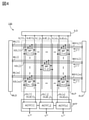
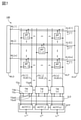
- FIG. 2 is a circuit diagram showing a configuration example of a semiconductor device.
- FIG. 3 is a circuit diagram showing a configuration example of a semiconductor device.
- FIG. 4 is a circuit diagram showing a configuration example of a semiconductor device.
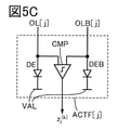
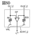
- Each of FIGS. 5A to 5F is a circuit diagram showing a configuration example of a circuit included in the semiconductor device.
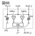
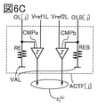
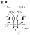
- FIGS. 6A to 6F is a circuit diagram showing a configuration example of a circuit included in the semiconductor device.
- FIG. 7 is a circuit diagram showing a configuration example of a semiconductor device.
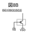
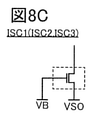
- FIGS. 8A to 8D is a circuit diagram showing a configuration example of a circuit included in the semiconductor device.
- FIGS. 8A to 8D is a circuit diagram showing a configuration example of a circuit included in the semiconductor device.
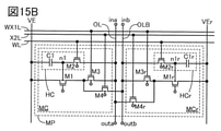
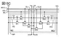
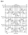
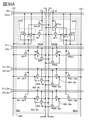
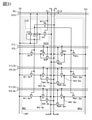
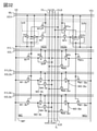
- FIGS. 15A to 15C is a circuit diagram showing a configuration example of a circuit included in the semiconductor device.
- 16A and 16B are circuit diagrams showing a configuration example of a circuit included in the semiconductor device.
- FIGS. 15A to 15C is a circuit diagram showing a configuration example of a circuit included in the semiconductor device.
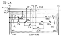
- FIG. 17A to 17C is a circuit diagram showing a configuration example of a circuit included in the semiconductor device.
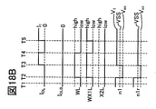
- FIGS. 18A to 18C is a timing chart illustrating an operation example of the semiconductor device.
- FIGS. 19A to 19C is a timing chart illustrating an operation example of the semiconductor device.
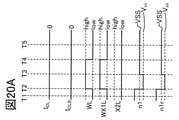
- 20A to 20C are timing charts illustrating operation examples of the semiconductor device.
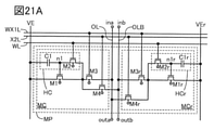
- 21A and 21B are circuit diagrams showing a configuration example of a circuit included in the semiconductor device.
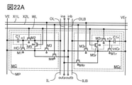
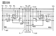
- 22A and 22B are circuit diagrams showing a configuration example of a circuit included in the semiconductor device.
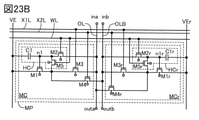
- 23A and 23B are circuit diagrams showing a configuration example of a circuit included in the semiconductor device.
- FIG. 24 is a circuit diagram showing a configuration example of a circuit included in the semiconductor device.
- FIG. 25 is a circuit diagram showing a configuration example of a circuit included in the semiconductor device.
- FIG. 26 is a circuit diagram showing a configuration example of a circuit included in the semiconductor device.
- FIG. 27 is a circuit diagram showing a configuration example of a circuit included in the semiconductor device.
- FIG. 28 is a circuit diagram showing a configuration example of a circuit included in the semiconductor device.
- FIG. 29 is a circuit diagram showing a configuration example of a circuit included in the semiconductor device.
- 30A and 30B are circuit diagrams showing a configuration example of a circuit included in the semiconductor device.
- FIG. 31 is a circuit diagram showing a configuration example of a circuit included in the semiconductor device.
- FIG. 32 is a circuit diagram showing a configuration example of a circuit included in the semiconductor device.
- FIG. 33 is a circuit diagram showing a configuration example of a circuit included in the semiconductor device.
- FIG. 34 is a circuit diagram showing a configuration example of a circuit included in the semiconductor device.
- FIG. 35 is a circuit diagram showing a configuration example of a circuit included in the semiconductor device.
- FIG. 36 is a circuit diagram showing a configuration example of a circuit included in the semiconductor device.
- FIG. 37 is a circuit diagram showing a configuration example of a circuit included in the semiconductor device.
- FIG. 38 is a circuit diagram showing a configuration example of a circuit included in the semiconductor device.
- FIG. 39 is a circuit diagram showing a configuration example of a circuit included in the semiconductor device.
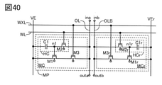
- FIG. 40 is a circuit diagram showing a configuration example of a circuit included in a semiconductor device.
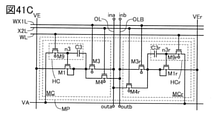
- FIG. 41A to 41C is a circuit diagram showing a configuration example of a circuit included in the semiconductor device.
- FIG. 42 is a circuit diagram showing a configuration example of a circuit included in the semiconductor device.
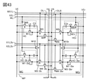
- FIG. 43 is a circuit diagram showing a configuration example of a circuit included in the semiconductor device.
- FIG. 44 is a circuit diagram showing a configuration example of a circuit included in the semiconductor device.
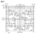
- FIG. 45 is a circuit diagram showing a configuration example of a circuit included in the semiconductor device.
- FIG. 46 is a circuit diagram showing a configuration example of a circuit included in the semiconductor device.
- 47A and 47B are circuit diagrams showing a configuration example of a circuit included in the semiconductor device.
- FIG. 48 is a circuit diagram showing a configuration example of a circuit included in the semiconductor device. Each of FIGS.
- FIG. 49A to 49C is a timing chart illustrating an operation example of the semiconductor device.
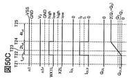
- FIGS. 50A to 50C is a timing chart illustrating an operation example of the semiconductor device.
- FIG. 51 is a circuit diagram showing a configuration example of a circuit included in the semiconductor device.
- FIG. 52 is a circuit diagram showing a configuration example of a circuit included in the semiconductor device.
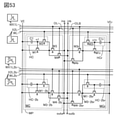
- FIG. 53 is a circuit diagram showing a configuration example of a circuit included in the semiconductor device.
- FIG. 54 is a circuit diagram showing a configuration example of a circuit included in the semiconductor device.
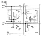
- 55A and 55B are circuit diagrams showing a configuration example of a circuit included in the semiconductor device.
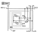
- FIGS. 56A to 56C is a circuit diagram showing a configuration example of a circuit included in the semiconductor device.
- FIG. 57A and 57B are circuit diagrams showing a configuration example of a circuit included in the semiconductor device.
- FIG. 58 is a circuit diagram showing a configuration example of a circuit included in the semiconductor device.
- 59A and 59B are circuit diagrams showing a configuration example of a circuit included in the semiconductor device.
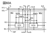
- 60A and 60B are circuit diagrams showing a configuration example of a circuit included in the semiconductor device.
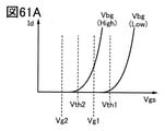
- 61A and 61B are diagrams showing voltage-current characteristics of a transistor included in a semiconductor device.
- FIG. 62 is a circuit diagram showing a configuration example of a circuit included in the semiconductor device.
- FIG. 63 is a circuit diagram showing a configuration example of a circuit included in the semiconductor device.
- FIG. 64 is a circuit diagram showing a configuration example of a circuit included in the semiconductor device.
- FIG. 65 is a circuit diagram showing a configuration example of a circuit included in the semiconductor device.
- FIG. 66 is a block diagram showing a configuration example of CNN.
- FIG. 67A is a diagram showing a configuration example of pixels
- FIG. 67B is a diagram showing a configuration example of a filter.
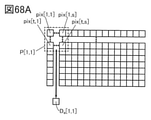
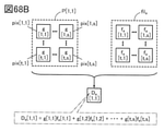
- 68A and 68B are diagrams illustrating an example of the convolution process.
- FIG. 69 is a diagram illustrating an example of the convolution process.
- FIG. 70 is a diagram showing a configuration example of a feature map.
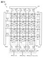
- FIG. 71 is a block diagram illustrating an example of a semiconductor device that performs an operation of a convolution process.
- FIG. 72 is a block diagram illustrating an example of a semiconductor device that performs an operation of a convolution process.
- FIG. 73 is a block diagram illustrating an example of a semiconductor device that performs an operation of a convolution process.
- FIG. 74 is a block diagram illustrating an example of a semiconductor device that performs an operation of a convolution process.
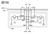
- 75A and 75B are circuit diagrams showing a configuration example of a circuit included in the semiconductor device.
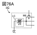
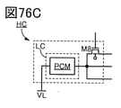
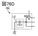
- 76A to 76D are circuit diagrams showing a configuration example of a circuit included in the semiconductor device.
- FIG. 77 is a schematic cross-sectional view showing a configuration example of a semiconductor device.
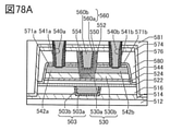
- 78A to 78C are schematic cross-sectional views showing a configuration example of a transistor.
- FIG. 79 is a schematic cross-sectional view showing a configuration example of a semiconductor device.
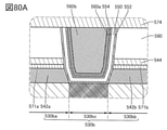
- 80A and 80B are schematic cross-sectional views showing a configuration example of a transistor.
- FIG. 81 is a schematic cross-sectional view showing a configuration example of a transistor.
- FIG. 82A is a diagram for explaining the classification of the crystal structure of IGZO
- FIG. 82B is a diagram for explaining the XRD spectrum of crystalline IGZO
- FIG. 82C is a diagram for explaining the microelectron diffraction pattern of crystalline IGZO.
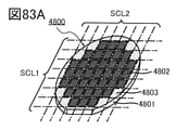
- .. 83A is a perspective view showing an example of a semiconductor wafer
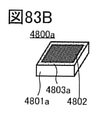
- FIG. 83B is a perspective view showing an example of a chip
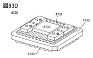
- FIGS. 83C and 83D are perspective views showing an example of an electronic component.
- FIG. 84 is a perspective view showing an example of an electronic device.
- 85A to 85C are perspective views showing an example of an electronic device.
- the synaptic connection strength can be changed by giving existing information to the neural network.
- the process of giving existing information to the neural network and determining the bond strength may be called "learning”.
- neural network models include Hopfield type and hierarchical type.
- a neural network having a multi-layer structure may be referred to as a “deep neural network” (DNN), and machine learning by a deep neural network may be referred to as “deep learning”.
- DNN deep neural network
- machine learning by a deep neural network may be referred to as “deep learning”.
- a metal oxide is a metal oxide in a broad sense. Metal oxides are classified into oxide insulators, oxide conductors (including transparent oxide conductors), oxide semiconductors (also referred to as Oxide Semiconductor or simply OS) and the like. For example, when a metal oxide is contained in the channel forming region of a transistor, the metal oxide may be referred to as an oxide semiconductor. That is, when a metal oxide can form a channel forming region of a transistor having at least one of an amplification action, a rectifying action, and a switching action, the metal oxide is referred to as a metal oxide semiconductor. be able to. Further, when the term "OS transistor" is used, it can be rephrased as a transistor having a metal oxide or an oxide semiconductor.
- a metal oxide having nitrogen may also be collectively referred to as a metal oxide. Further, the metal oxide having nitrogen may be referred to as a metal oxynitride.
- the configuration shown in each embodiment can be appropriately combined with the configuration shown in other embodiments to form one aspect of the present invention. Further, when a plurality of configuration examples are shown in one embodiment, the configuration examples can be appropriately combined with each other.
- the content described in one embodiment (may be a part of the content) is different from the content described in the embodiment (may be a part of the content) and one or more different implementations. It is possible to apply, combine, or replace at least one content with the content described in the form of (may be a part of the content).
- figure (which may be a part) described in one embodiment is different from another part of the figure, another figure (which may be a part) described in the embodiment, and one or more different figures.
- the figure (which may be a part) described in the embodiment is different from another part of the figure, another figure (which may be a part) described in the embodiment, and one or more different figures.
- more figures can be formed.
- the code is used for identification such as "_1", “[n]”, “[m, n]”. May be added and described. Further, in the drawings and the like, when the reference numerals such as “_1”, “[n]” and “[m, n]” are added to the reference numerals, when it is not necessary to distinguish them in the present specification and the like, when it is not necessary to distinguish them.
- the identification code may not be described.
- a hierarchical neural network has one input layer, one or more intermediate layers (hidden layers), and one output layer, and is composed of a total of three or more layers.
- the hierarchical neural network 100 shown in FIG. 1A shows an example thereof, and the neural network 100 has a first layer to an R layer (R here can be an integer of 4 or more). ing.
- R can be an integer of 4 or more
- the first layer corresponds to the input layer
- the R layer corresponds to the output layer
- the other layers correspond to the intermediate layer.
- FIG. 1A illustrates the (k-1) th layer and the kth layer (here, k is an integer of 3 or more and R-1 or less) as the intermediate layer, and the other intermediate layers. Is not shown.
- Each layer of the neural network 100 has one or more neurons.
- the first layer has neurons N 1 (1) to neurons N p (1) (where p is an integer of 1 or more), and the layer (k-1) has neurons N 1. (K-1) to neuron N m (k-1) (where m is an integer of 1 or more), and the kth layer is neuron N 1 (k) to neuron N n (k) ( Here, n is an integer of 1 or more), and the layer R has neurons N 1 (R) to neurons N q (R) (where q is an integer of 1 or more). ..
- Figure 1B is a neuron N j of the k-th layer (k), shows the signal which is input to the neuron N j (k), a signal output from the neuron N j (k), the.
- the degree of signal transmission is determined by the strength of synaptic connections (hereinafter referred to as weighting factors) that connect these neurons.
- weighting factors the strength of synaptic connections that connect these neurons.
- the signal output from the neurons in the previous layer is multiplied by the corresponding weighting factor and input to the neurons in the next layer.
- i an integer 1 or m
- the signal input to the neuron Nj (k) in the kth layer can be expressed by the equation (1.1).
- the signal is used.
- a weighting coefficient w 1 (k-1) j (k) to w m (k-1) j (k) corresponding to each signal is used. Is multiplied.
- the neurons N j (k) in the k-th layer have w 1 (k-1) j (k) ⁇ z 1 (k-1) to w m (k-1) j (k) ⁇ z m (k-1).
- k-1) is input.
- the total sum u j (k) of the signals input to the neurons N j (k) in the k-th layer is given by Eq. (1.2).
- the result of the sum of products may be biased as a bias.
- the bias is b
- the equation (1.2) can be rewritten as the following equation.
- the neuron N j (k) produces an output signal z j (k) in response to u j (k).
- the output signal z j (k) from the neuron N j (k) is defined by the following equation.
- the function f (u j (k) ) is an activation function in a hierarchical neural network, and a step function, a ramp function (ReLU function), a sigmoid function, a tanh function, a softmax function, and the like can be used.
- the activation function may be the same or different in all neurons.
- the activation function of neurons may be the same or different in each layer.
- the signal output by the neurons in each layer, the weighting factor w, or the bias b may be an analog value or a digital value.
- the digital value may be, for example, a binary value or a ternary value. A value with a larger number of bits may be used.
- an analog value for example, a linear ramp function, a sigmoid function, or the like may be used as the activation function.
- binary digital values for example, a step function with an output of -1 or 1 or 0 or 1 may be used.
- the signal output by the neuron in each layer may have three or more values.
- the activation function that outputs three values is, for example, a step function having three or more values, for example, an output of -1, 0, or 1.
- a step function or the like with 0, 1, or 2 may be used.
- a step function of -2, -1, 0, 1, or 2 may be used.
- the neural network 100 By inputting an input signal to the first layer (input layer), the neural network 100 is sequentially input from the front layer in each layer from the first layer (input layer) to the last layer (output layer). Based on the signal, an output signal is generated using the equation (1.1), the equation (1.2) (or the equation (1.3)), and the equation (1.4), and the output signal is transferred to the next layer. Perform the operation to output to. The signal output from the last layer (output layer) corresponds to the result calculated by the neural network 100.
- the weight coefficient of the synapse circuit of the neural network 100 is binary (a combination of “-1” and “+1”, a combination of “0”, “+1”, etc.), and 3 A value (a combination of "-1", “0”, “1”, etc.) or a multi-value of 4 or more values (in the case of 5 values, "-2", “-1", “0”, “1” , “2” combination, etc.), and the activation function of the neuron is binary ("-1", "+1” combination, or "0", "+1” combination, etc.), trivalent (“-1").
- weighting coefficient and the calculated value of the synaptic circuit of the neural network 100 are not limited to digital values, and analog values can be used for at least one of them.
- the arithmetic circuit 110 shown in FIG. 2 is, for example, a semiconductor device including an array unit ALP, a circuit ILD, a circuit WLD, a circuit XLD, and a circuit AFP.
- the arithmetic circuit 110 transmits signals z 1 (k-1) to z m (k-1) input to neurons N 1 (k) to neurons N n (k) in the kth layer in FIGS. 1A and 1B. It is a circuit which processes and generates the signal z 1 (k) to z n (k) output from each of the neuron N 1 (k) to the neuron N n (k).
- the entire or part of the arithmetic circuit 110 may be used for purposes other than neural networks, AI, and the like.
- the entire operation circuit 110 or a part thereof. May be used for processing. That is, not only the calculation for AI but also the whole or a part of the arithmetic circuit 110 may be used for general calculation.
- the circuit ILD is electrically connected to the wiring IL [1] to the wiring IL [n] and the wiring ILB [1] to the wiring ILB [n].
- the circuit WLD is electrically connected to the wiring WLS [1] to the wiring WLS [m].
- the circuit XLD is electrically connected to the wiring XLS [1] to the wiring XLS [m].
- the circuit AFP is electrically connected to the wiring OL [1] to the wiring OL [n] and the wiring OLB [1] to the wiring OLB [n].
- the array unit ALP has m ⁇ n circuit MPs as an example.
- the circuit MP is arranged in a matrix of m rows and n columns in the array unit ALP.
- the circuit MP located in the i-row j column (where i is an integer of 1 or more and m or less and j is an integer of 1 or more and n or less) is referred to as a circuit MP [i, It is written as j].
- FIG. 2 only the circuit MP [1,1], the circuit MP [m, 1], the circuit MP [i, j], the circuit MP [1, n], and the circuit MP [m, n] are shown.
- Other circuit MPs are not shown.
- the circuit MP [i, j] includes wiring IL [j], wiring ILB [j], wiring WLS [i], wiring XLS [i], wiring OL [j], and wiring OLB [ j] and are electrically connected to.
- the circuit MP [i, j] may be referred to as a weighting coefficient (either the first data or the second data ) between the neuron N i (k-1) and the neuron N j (k).
- it has a function of holding (referred to as first data).
- the circuit MP [i, j] has information (for example, potential, resistance value, current) according to the first data (weight coefficient) input from the wiring IL [j] and the wiring ILB [j]. (Value, etc.) is retained.
- the circuit MP [i, j] may be referred to as neuron N i (k-1) signal is output from the z i (k-1) (the first data or the other of the second data.
- the second data has a function of outputting the product of the first data (referred to as the second data).
- the second data z i (k-1) is input from the wiring XLS [i], so that the product of the first data and the second data is obtained.
- the corresponding information for example, current, voltage, etc.
- the information related to the product of the first data and the second data for example, current, voltage, etc.
- the wiring IL [j] and the wiring ILB [j] are arranged is shown, one aspect of the present invention is not limited to this. Only one of the wiring IL [j] and the wiring ILB [j] may be arranged.
- the circuit ILD has a circuit MP [1, 1] to a circuit MP [m, via a wiring IL [1] to a wiring IL [n] and a wiring ILB [1] to a wiring ILB [n].
- information eg, potential, resistance value, etc.
- w 1 (k-1) 1 (k) to w m (k-1) n (k) which is a weighting coefficient. It has a function to input the current value etc.).
- the circuit ILD the information with respect to the circuit MP [i, j], corresponding to the first data w i is a weighting factor (k-1) j (k ) ( e.g., potential, resistance The value, current value, etc.) is supplied by the wiring IL [j] and the wiring ILB [j].
- k-1 j (k ) e.g., potential, resistance
- circuit XLD has a neuron N 1 (k-1 ) for each of the circuits MP [1, 1] to the circuit MP [m, n] via the wiring XLS [1] to the wiring XLS [m]. ) To the second data z 1 (k-1) to z m (k-1) corresponding to the calculated value output from the neuron N m (k-1) .
- circuit XLD is circuit MP [i, 1] to circuit MP [i, n] relative to neuron N i (k-1) second data z i outputted from the (k-1) Information corresponding to (for example, potential, current value, etc.) is supplied by the wiring XLS [i].
- the wiring XLS [i] may be a plurality of wirings.
- FIG. 3 shows an arithmetic circuit having a configuration in which the wiring XLS [i] electrically connected to the circuit MP [i, j] of the arithmetic circuit 110 is replaced with two wirings X1L and X2L. Shows 120.
- the wiring XLS [i] is arranged is shown, one aspect of the present invention is not limited to this.
- a wiring for transmitting an inverted signal of the signal input to the wiring XLS [i] may be separately arranged.
- the circuit WLD has a function of selecting a circuit MP to which information (for example, potential, resistance value, current value, etc.) corresponding to the first data input from the circuit ILD is written. For example, when writing information (for example, potential, resistance value, current value, etc.) to the circuit MP [i, 1] to the circuit MP [i, n] located in the i-th row of the array unit ALP, the circuit WLD For example, a signal for turning the write switching element included in the circuit MP [i, 1] to the circuit MP [i, n] into an on state or an off state is supplied to the wiring WLS [i], except for the i-th line.
- information for example, potential, resistance value, current value, etc.
- the potential for turning off the writing switching element included in the circuit MP of the above circuit MP may be supplied to the wiring WLS.
- the wiring WLS [i] is arranged, one aspect of the present invention is not limited to this.
- a wiring for transmitting an inverted signal of the signal input to the wiring WLS [i] may be separately arranged.
- the wiring WLS [i] may be replaced with a plurality of wirings.
- the wiring X1L [i] of the arithmetic circuit 120 of FIG. 3 may also be used as a selection signal line for writing information to the circuit MP [i, 1] to the circuit MP [i, n].
- the wiring X1L [i] of the arithmetic circuit 120 is regarded as the wiring WX1L [i], and the wiring WX1L is electrically connected to the circuit WLD and the circuit XLD. It may have been done.
- the wiring WX1L [i] is supplied with a signal for turning on or off the writing switching element included in the circuit MP [i, 1] to the circuit MP [i, n] from the circuit WLD.
- the circuit XLD preferably has a function of making a non-conducting state between the circuit XLD and the wiring WX1L.
- the second data z 1 (k-1) to z m corresponding to the calculated values output from the neurons N 1 (k-1) to the neurons N m (k-1) via the wiring WX1L [i].
- the circuit WLD has a function of making the circuit WLD and the wiring WX1L non-conducting. It is preferable to have.
- the circuit AFP has, for example, a circuit ACTF [1] to a circuit ACTF [n].
- the circuit ACTF [j] is electrically connected to each of the wiring OL [j] and the wiring OLB [j].
- the circuit ACTF [j] generates a signal corresponding to each information (for example, potential, current value, etc.) input from the wiring OL [j] and the wiring OLB [j].
- the respective information for example, potential, current value, etc.
- the wiring OL [j] and the wiring OLB [j] is compared, and a signal corresponding to the comparison result is generated.
- the signal corresponds to the signal z j (k) output from the neuron N j (k) .
- the circuit ACTF [1] to the circuit ACTF [n] functions, for example, as a circuit for performing the calculation of the activation function of the neural network described above.
- the circuit ACTF [1] to the circuit ACTF [n] may have a function of converting an analog signal into a digital signal.
- the circuit ACTF [1] to the circuit ACTF [n] may have a function of amplifying and outputting an analog signal, that is, a function of converting an output impedance.
- the circuit ACTF [1] to the circuit ACTF [n] may have a function of converting a current or an electric charge into a voltage.
- the circuit ACTF [j] may have a function of initializing the potentials of the wiring OL [j] and the wiring OLB [j].
- the circuit ACTF In the arithmetic circuit 110, the arithmetic circuit 120, and the arithmetic circuit 130 shown in FIGS. 2 to 4, examples of the case where the circuit ACTF is arranged are shown, but one aspect of the present invention is not limited thereto. ..
- the circuit ACTF may not be arranged in the circuit AFP.
- FIG. 5A is a circuit that generates a signal z j (k) according to a current input from the wiring OL [j] and the wiring OLB [j].
- FIG. 5A shows an example of an operation circuit of an activation function that outputs an output signal z j (k) represented by a binary value.
- the circuit ACTF [j] has, for example, a resistor RE, a resistor REB, and a comparator CMP.
- the resistance RE and the resistance REB have a function of converting a current into a voltage. Therefore, any element or circuit having a function of converting a current into a voltage is not limited to a resistor.
- the wiring OL [j] is electrically connected to the first terminal of the resistor RE and the first input terminal of the comparator CMP, and the wiring OLB [j] is connected to the first terminal of the resistor REB and the comparator CMP. It is electrically connected to the second input terminal.
- the second terminal of the resistance RE is electrically connected to the wiring VAL
- the second terminal of the resistance REB is electrically connected to the wiring VAL.
- the second terminal of the resistance RE and the second terminal of the resistance REB may be connected to the same wiring. Alternatively, it may be connected to another wiring having the same potential.
- the resistance values of the resistance RE and the resistance REB are equal to each other.
- the difference between the resistance values of the resistance RE and the resistance REB is within 10%, more preferably within 5% of the resistance value of the resistance RE.
- one aspect of the present invention is not limited to this. In some cases, or depending on the situation, the resistance values of the resistors RE and the resistors REB may be different from each other.
- Wiring VAL functions as wiring that gives a constant voltage, for example.
- the constant voltage may be, for example, VDD, which is a high level potential, VSS, which is a low level potential, or ground potential (GND). Further, it is preferable to appropriately set the constant voltage according to the configuration of the circuit MP. Further, for example, a pulse signal may be supplied to the wiring VAL instead of a constant voltage.
- the voltage between the first terminal and the second terminal of the resistance RE is determined according to the current flowing from the wiring OL [j]. Therefore, the resistance value of the resistor RE and the voltage corresponding to the current are input to the first input terminal of the comparator CMP.
- the voltage between the first terminal and the second terminal of the resistor REB is determined according to the current flowing from the wiring OLB [j]. Therefore, the resistance value of the resistor REB and the voltage corresponding to the current are input to the second input terminal of the comparator CMP.
- the comparator CMP has a function of comparing the voltages input to each of the first input terminal and the second input terminal and outputting a signal from the output terminal of the comparator CMP according to the comparison result.
- the comparator CMP outputs a high level potential from the output terminal of the comparator CMP when the voltage input to the second input terminal is higher than the voltage input to the first input terminal, and the second input terminal.
- the low level potential can be output from the output terminal of the comparator CMP.
- the output signal z j (k) output by the circuit ACTF [j] should be a binary value.
- each of the high level potential and the low level potential output from the output terminal of the comparator CMP can correspond to "+1" and "-1” as the output signal zj (k).
- the high level potential and the low level potential output from the output terminal of the comparator CMP may correspond to "+1" and "0” as the output signal zj (k), respectively.
- the resistance RE and the resistance REB are used, but the resistance is not limited as long as it is an element or circuit having a function of converting a current into a voltage. Therefore, the resistance RE and the resistance REB of the circuit ACTF [j] of FIG. 5A can be replaced with another circuit element.
- the circuit ACTF [j] shown in FIG. 5B is a circuit in which the resistance RE and the resistance REB included in the circuit ACTF [j] of FIG. 5A are replaced with the capacitance CE and the capacitance CEB, and the circuit ACTF [j] of FIG. ], Almost the same operation can be performed.
- the capacitance values of the capacitance CE and the capacitance CEB are equal to each other.
- the difference between the capacitance values of the capacitance CE and the capacitance CEB is within 10%, more preferably within 5% of the capacitance value of the capacitance CE.
- a circuit for initializing the electric charge accumulated in the capacitance CE and the capacitance CEB may be provided.
- a switch may be provided in parallel with the capacitance CE.
- the second terminal of the switch is connected to the wiring VAL, and the first terminal of the switch is connected to the first terminal of the capacitance CE, the wiring OL [j], and the first input terminal of the comparator CMP. May be good.
- the second terminal of the switch is connected to a wiring different from the wiring VAL, and the first terminal of the switch is connected to the first terminal of the capacitance CE, the wiring OL [j], and the first input terminal of the comparator CMP. It may be connected.
- the circuit ACTF [j] shown in FIG. 5C is a circuit in which the resistor RE and the resistor REB included in the circuit ACTF [j] of FIG.
- comparator CMP included in the circuit ACTF [j] of FIGS. 5A to 5C can be replaced with an operational amplifier OP as an example.
- the circuit ACTF [j] shown in FIG. 5D shows a circuit diagram in which the comparator CMP of the circuit ACTF [j] of FIG. 5A is replaced with an operational amplifier OP.
- the switch S01a and the switch S01b may be provided in the circuit ACTF [j] of FIG. 5B.
- the circuit ACTF [j] can hold the potential corresponding to the current input from the wiring OL [j] and the wiring OLB [j] to the capacitance CE and the capacitance CEB, respectively.
- the wiring OL [j] is electrically connected to the first terminal of the switch S01a, and the second terminal of the switch S01a is compared with the first terminal of the capacitance CE.
- the first input terminal of the CMP is electrically connected
- the wiring OLB [j] is electrically connected to the first terminal of the switch S01b
- the first terminal of the capacitance CEB and the comparison device are connected to the second terminal of the switch S01b.
- the configuration may be such that the second input terminal of the CMP is electrically connected.
- the switches S01a and the switch S01b are used. This can be done by turning each on.
- the potentials input to the first input terminal and the second input terminal of the comparator CMP can be held in the capacitance CE and the capacitance CEB.
- the switch S01a and the switch S01b for example, an electric switch such as an analog switch or a transistor can be applied. Further, as the switch S01a and the switch S01b, for example, a mechanical switch may be applied.
- the transistor can be an OS transistor or a transistor having silicon in the channel forming region (hereinafter referred to as a Si transistor).
- the voltage values of the capacitance CE and the capacitance CEB can be controlled by controlling the period in which each of the switch S01a and the switch S01b is kept on. For example, when the current values flowing through the capacitance CE and the capacitance CEB are large, the voltage values of the capacitance CE and the capacity CEB become large by shortening the period in which each of the switch S01a and the switch S01b is kept on. You can prevent it from going too far.
- the comparator CMP included in the circuit ACTF [j] of FIGS. 5A to 5C and 5E can be, for example, a chopper type comparator.
- the comparator CMP shown in FIG. 5F shows a chopper type comparator, and the comparator CMP has a switch S02a, a switch S02b, a switch S03, a capacitance CC, and an inverter circuit INV3.
- the switch S02a, the switch S02b, and the switch S03 can be a transistor such as a mechanical switch, an OS transistor, or a Si transistor, similarly to the switch S01a and the switch S01b described above.
- the first terminal of the switch S02a is electrically connected to the terminal VinT
- the first terminal of the switch S02b is electrically connected to the terminal VrefT
- the second terminal of the switch S02a is the second terminal of the switch S02b. It is electrically connected to the first terminal of the capacity CC.
- the second terminal of the capacitance CC is electrically connected to the input terminal of the inverter circuit INV3 and the first terminal of the switch S03.
- the terminal VoutT is electrically connected to the output terminal of the inverter circuit INV3 and the second terminal of the switch S03.
- the terminal VinT functions as a terminal for inputting an input potential to the comparator CMP
- the terminal VrefT functions as a terminal for inputting a reference potential to the comparator CMP
- the terminal VoutT functions as an output potential from the comparator CMP. Functions as a terminal for outputting.
- the terminal VinT corresponds to either the first terminal or the second terminal of the comparator CMP of FIGS. 5A to 5C and 5E
- the terminal VrefT corresponds to the first terminal of the comparator CMP of FIGS. 5A to 5C and 5E. It can correspond to one terminal or the other of the second terminal.
- the circuit ACTF [j] of FIGS. 5A to 5E is an operation circuit of an activation function that outputs an output signal z j (k) represented by a binary value, whereas the circuit ACTF [j] is an output signal z j ( It may be configured to output k) as 3 or more values or as an analog value.
- 6A to 6F are circuits that generate a signal z j (k) according to the current input from the wiring OL [j] and the wiring OLB [j], and are output signals z j represented by three values.
- An example of an arithmetic circuit of an activation function that outputs (k) is shown.
- the circuit ACTF [j] shown in FIG. 6A has a resistance RE, a resistance REB, a comparator CMPa, and a comparator CMPb.
- the wiring OL [j] is electrically connected to the first terminal of the resistor RE and the first input terminal of the comparator CMPA, and the wiring OLB [j] is connected to the first terminal of the resistor REB and the comparator CMPb. It is electrically connected to the first input terminal.
- the second input terminal of the comparator CMPA and the second input terminal of the comparator CMPb are electrically connected to the wiring VrefL.
- the second terminal of the resistance RE is electrically connected to the wiring VAL
- the second terminal of the resistance REB is electrically connected to the wiring VAL.
- the wiring Vref L functions as a voltage line that gives a constant voltage Vref, and the Vref is preferably, for example, GND or more and VDD or less. Further, depending on the situation, the V ref may have a potential of less than GND or a potential of higher than VDD. V ref is treated as a reference potential (potential for comparison) in the comparator CMPa and the comparator CMPb.
- the voltage between the first terminal and the second terminal of the resistance RE is determined according to the current flowing from the wiring OL [j]. Therefore, the resistance value of the resistor RE and the voltage corresponding to the current are input to the first input terminal of the comparator CMPa.
- the voltage between the first terminal and the second terminal of the resistor REB is determined according to the current flowing from the wiring OLB [j]. Therefore, the resistance value of the resistor REB and the voltage corresponding to the current are input to the first input terminal of the comparator CMPb.
- the comparator CMPa compares the voltages input to each of the first input terminal and the second input terminal, and outputs a signal from the output terminal of the comparator CMPa according to the comparison result. For example, the comparator CMPa outputs a high level potential from the output terminal of the comparator CMPa when the voltage (V ref ) input to the second input terminal is higher than the voltage input to the first input terminal. When the voltage input to the first input terminal is higher than the voltage (V ref ) input to the second input terminal, the low level potential can be output from the output terminal of the comparator CMPa.
- the comparator CMPb compares the voltages input to each of the first input terminal and the second input terminal, and outputs a signal from the output terminal of the comparator CMPb according to the comparison result. do. For example, the comparator CMPb outputs a high level potential from the output terminal of the comparator CMPb when the voltage (V ref ) input to the second input terminal is higher than the voltage input to the first input terminal. When the voltage input to the first input terminal is higher than the voltage (V ref ) input to the second input terminal, the low level potential can be output from the output terminal of the comparator CMPb.
- the potentials output from the respective output terminals of the comparator CMPa and the comparator CMPb can be expressed as , for example, a ternary output signal z j (k).
- a ternary output signal z j (k) For example, the comparator high level voltage from the output terminal of CMPa is output, the comparator when the low-level potential from the output terminal of CMPb is output, the output signal z j (k) is "+1", and the output of the comparator CMPa low level potential is outputted from the terminal, when the high level potential is output from the output terminal of the comparator CMPb, the output signal z j (k) is set to "-1", a low-level potential from the output terminal of the comparator CMPa is output, when the low-level potential is output from the output terminal of the comparator CMPb, the output signal z j (k) may be a "0".
- the circuit ACTF [j] is not limited to the circuit configuration shown in FIG. 6A, and can be changed depending on the situation.
- a conversion circuit TRF may be provided in the circuit ACTF [j].
- the circuit ACTF [j] of FIG. 6B is a configuration example in which the conversion circuit TRF is provided in the circuit ACTF [j] of FIG. 6, and the output terminals of the comparator CMPa and the comparator CMPb are the input terminals of the converter circuit TRF. Is electrically connected to.
- a digital-to-analog conversion circuit in this case, the signal zj (k) is an analog value
- the like can be used.
- the wiring VrefL electrically connected to the second input terminals of the comparator CMPa and the comparator CMPb may be replaced with separate wirings of the wiring Vref1L and the wiring Vref2L.
- the second input terminal of the comparator CMPa included in the circuit ACTF [j] of FIG. 6A is electrically connected not to the wiring VrefL but to the wiring Vref1L, and the second input terminal of the comparator CMPb is electrically connected.
- the two input terminals are electrically connected to the wiring Vref2L instead of the wiring VrefL.
- an amplifier circuit, an impedance conversion circuit, or the like may be used as a configuration different from the circuit ACTF [j] of FIGS. 6A to 6C.
- the circuit ACTF [j] shown in FIG. 6D can be applied to the circuit AFP of the arithmetic circuit 110 of FIG.
- the circuit ACTF [j] of FIG. 6D has a resistor RE, a resistor REB, an operational amplifier OPa, and an operational amplifier OPb, and functions as an amplifier circuit.
- the wiring OL [j] is electrically connected to the first terminal of the resistor RE and the non-inverting input terminal of the operational amplifier OPa
- the wiring OLB [j] is the first terminal of the resistance REB and the non-inverting input terminal of the operational amplifier OPb. It is electrically connected to the input terminal.
- the inverting input terminal of the operational amplifier OPa is electrically connected to the output terminal of the operational amplifier OPa
- the inverting input terminal of the operational amplifier OPb is electrically connected to the output terminal of the operational amplifier OPb.
- the second terminal of the resistance RE is electrically connected to the wiring VAL
- the second terminal of the resistance REB is electrically connected to the wiring VAL.
- the operational amplifier OPa and the operational amplifier OPb included in the circuit ACTF [j] of FIG. 6D have a voltage follower connection configuration.
- the potential output from the output terminal of the operational amplifier OPa becomes almost equal to the potential input to the non-inverting input terminal of the operational amplifier OPa
- the potential output from the output terminal of the operational amplifier OPb is the non-inverting input of the operational amplifier OPb. It is almost equal to the potential input to the terminal.
- the output signal z j (k) is output from the circuit ACTF [j] as two analog values.
- the output terminal of the operational amplifier OPa and the output terminal of the operational amplifier OPb may be connected to the input terminal of the comparator CMP, respectively. Then, the output from the comparator CMP may be used as an output signal z j (k).
- an integrator circuit, a current-voltage conversion circuit, or the like may be used as a configuration different from the circuit ACTF [j] of FIGS. 6A to 6D.
- an operational amplifier may be used to configure an integrator circuit or a current-voltage conversion circuit.
- the circuit ACTF [j] shown in FIG. 6E can be applied to the circuit AFP of the arithmetic circuit 110 of FIG.
- the circuit ACTF [j] of FIG. 6E has an operational amplifier OPa, an operational amplifier OPb, a load LEa, and a load LEb.
- the wiring OL [j] is electrically connected to the first input terminal (for example, the inverting input terminal) of the operational amplifier OPa and the first terminal of the load LEa, and the wiring OLB [j] is the first terminal of the operational amplifier OPb.
- the input terminal (for example, the inverting input terminal) and the first terminal of the load LEb are electrically connected.
- the second input terminal (for example, non-inverting input terminal) of the operational amplifier OPa is electrically connected to the wiring Vref1L
- the second input terminal (for example, the non-inverting input terminal) of the operational amplifier OPb is electrically connected to the wiring Vref2L. It is connected to the.
- the second terminal of the load LEa is electrically connected to the output terminal of the operational amplifier OPa
- the second terminal of the load LEb is electrically connected to the output terminal of the operational amplifier OPb.
- the wiring Vref1L and the wiring Vref2L here function as wirings that supply equal or different voltages to each other. Therefore, the wiring Vref1L and the wiring Vref2L may be combined into one wiring.
- the load LEa and the load LEb may be, for example, a resistance or a capacitance.
- the operational amplifier OPa and the load LEa, and the operational amplifier OPb and the load LEb each function as an integrator circuit. That is, electric charges are stored in the respective capacities (load LEa, load LEb) according to the amount of current flowing through the wiring OL [j] or the wiring OLB [j]. That is, the current flowing from the wiring OL [j] and the wiring OLB [j] is converted into a voltage by the integrated circuit and output as a signal z j (k).
- the output terminal of the operational amplifier OPa and the output terminal of the operational amplifier OPb may be connected to the input terminal of the comparator CMP, respectively. Then, the output from the comparator CMP may be used as an output signal z j (k).
- a circuit for initializing the charges accumulated in the capacities of the load LEa and the load LEb may be provided.
- a switch may be provided in parallel with the load LEa (capacity). That is, the second terminal of the switch is connected to the output terminal of the operational amplifier OPa, and the first terminal of the switch is connected to the wiring OL [j] and the first input terminal (for example, the inverting input terminal) of the operational amplifier OPa. May be.
- the load LEa and the load LEb have resistances other than the capacitance. Can be used.
- the circuit ACTF [j] shown in FIG. 6F can be applied to the circuit AFP of the arithmetic circuit 110 of FIG. 2 as a configuration different from the circuit ACTF [j] of FIGS. 6A to 6E.
- the circuit ACTF [j] of FIG. 6F has a resistor RE, a resistor REB, an analog-to-digital conversion circuit ADCa, and an analog-to-digital conversion circuit ADCb.
- the wiring OL [j] is electrically connected to the input terminal of the analog-to-digital conversion circuit ADCa and the first terminal of the resistor RE, and the wiring OLB [j] is connected to the input terminal of the analog-to-digital conversion circuit ADCb and the resistor. It is electrically connected to the first terminal of the REB.
- the second terminal of the resistance RE is electrically connected to the wiring VAL, and the second terminal of the resistance REB is electrically connected to the wiring VAL.
- the potentials of the first terminals of the resistance RE and the resistance REB are determined according to the currents flowing from the wiring OL [j] and the OLB [j]. Then, the circuit ACTF [j] converts the potential, which is an analog value, into a digital value of two values or three or more values (for example, 256 values) by the analog digital conversion circuit ADCa and the analog digital conversion circuit ADCb. , Has a function of outputting as a signal z j (k).
- the resistance RE and resistance REB shown in FIGS. 6A to 6D and 6F can be replaced with the capacitance CE, the capacitance CEB, or the diode element DE and the diode element DEB, as in FIGS. 5B and 5C.
- the wiring OL [j] is further provided by providing the switch S01a and the switch S01b in the same manner as in FIG. 5E. , The potential input from the wiring OLB [j] can be held.
- each of the arithmetic circuit 110, the arithmetic circuit 120, and the arithmetic circuit 130 shown in FIGS. 2 to 4 examples of cases where the wiring IL, the wiring ILB, the wiring OL, and the wiring OLB are arranged are shown.
- the embodiment is not limited to this.
- each of the arithmetic circuit 110, the arithmetic circuit 120, and the arithmetic circuit 130 may be configured such that the wiring IL and the wiring OL are combined as one wiring, and the wiring ILB and the wiring OLB are combined as one wiring. ..
- FIG. 7 shows the specific configuration.
- the arithmetic circuit 140 shown in FIG. 7 has a switching circuit TW [1] to a switching circuit TW [n].
- Each of the switching circuit TW [1] to the switching circuit TW [n] has a terminal TSa, a terminal TSaB, a terminal TSb, a terminal TSbB, a terminal TSc, and a terminal TScB.
- the terminal TSa is electrically connected to the wiring OL [j]
- the terminal TSb is electrically connected to the circuit ILD
- the terminal TSc is electrically connected to the circuit ACTF [j].
- the terminal TSaB is electrically connected to the wiring OLB [j]
- the terminal TSbB is electrically connected to the circuit ILD
- the terminal TScB is electrically connected to the circuit ACTF [j].
- the switching circuit TW [j] has a function of making the terminal TSa conductive between one of the terminal TSb or the terminal TSc and making the terminal TSa non-conducting between the terminal TSb or the other terminal TSc. .. Further, the switching circuit TW [j] has a function of making a conductive state between the terminal TSaB and one of the terminal TSbB or the terminal TScB, and making a non-conducting state between the terminal TSaB and the other of the terminal TSbB or the terminal TScB. Have.
- the terminal TSa and the terminal TSb are made conductive, and the terminal TSaB and the terminal TSbB are connected.
- the circuit MP [1, j] to the circuit MP [m, j] can be selected from the circuit ILD via the wiring OL [j] or the wiring OLB [j].
- Information corresponding to 1 data w 1 (k-1) 1 (k) to w m (k-1) n (k) (for example, potential, resistance value, current value, etc.) can be supplied.
- the circuit ACTF [j] obtains the result of the product sum (equation (1.2)) of the weighting coefficient and the signal of the neuron calculated by the circuit MP [1, j] to the circuit MP [m, j]. If this is the case, in the switching circuit TW [j], the wiring OL [j] and the wiring OLB [j] are made to be in a conductive state between the terminal TSa and the terminal TSc and in a conductive state between the terminal TSaB and the terminal TScB. Information (for example, potential, current value, etc.) according to the result of the sum of products can be supplied from [j] to the circuit ACTF [j]. Further, in the circuit ACTF [j], the value of the activation function is calculated from the result of the input sum of products, and the signal z j (k) can be obtained as the output signal of the neuron.
- Information for example, potential, current value, etc.
- FIG. 8A shows a configuration example of the switching circuit TW [j] and the circuit ILD, which can be applied to the arithmetic circuit 140. Note that FIG. 8A also illustrates the wiring OL [j], the wiring OLB [j], and the circuit AFP in order to show the configuration of the electrical connection between the switching circuit TW [j] and the circuit ILD. ing.
- the changeover circuit TW [j] has, for example, a switch SWI, a switch SWIB, a switch SWO, a switch SWOB, a switch SWL, a switch SWLB, a switch SWH, and a switch SWHB.
- the circuit ILD has a current source circuit ISC as an example.
- the current source circuit ISC may not be provided and a voltage source circuit may be arranged instead.
- the current source circuit ISC has a function of passing a current corresponding to a weighting coefficient (first data) input to the circuit MP to the wiring OL [j] and / or the wiring OLB [j].
- at least one current source circuit ISC may be arranged as a circuit for wiring OL [j] and a circuit for wiring OLB [j] as separate circuits.
- at least one current source circuit ISC may be provided for a set of wiring OL [j] and wiring OLB [j].
- the current source circuit ISC has one or a plurality of constant current sources, and in FIG. 8A, as an example, the constant current source circuit ISC1 and the constant current source circuit ISC2 are used as a plurality of constant current sources. It has a constant current source circuit ISC3. Further, as an example, the current source circuit ISC has a plurality of switches for selecting a plurality of constant current sources. In FIG. 8A, the switch SWC1, the switch SWC2, and the switch SWC3 are used as the plurality of switches. And have. When the current source circuit ISC has only one constant current source, the current source circuit ISC does not have to have a switch.
- the switch SWC1 and the switch SWC2 are used.
- the switch SWC3 may not be provided.
- the current flowing through each of the wiring OL [j] and the wiring OLB [j] is generated by the same current source circuit ISC as shown in FIG. 8A.
- the characteristics of the transistor may vary due to the manufacturing process of the transistor, which is different. Performance may differ between current source circuits.
- the same current source circuit it is possible to supply a current of the same magnitude to the wiring OL [j] and the wiring OLB [j], and the calculation accuracy can be improved.
- the switch SWI, switch SWIB, switch SWO, switch SWOB, switch SWL, switch SWLB, switch SWH, switch SWHB, switch SWC1, switch SWC2, and switch SWC3 described with reference to FIG. 8A include, for example, switch S01a and switch S01b.
- analog switches, electric switches such as transistors, mechanical switches, and the like can be applied.
- the terminal TSa electrically connects to the first terminal of the switch SWI, the first terminal of the switch SWO, the first terminal of the switch SWL, and the first terminal of the switch SWH. It is connected.
- the terminal TSaB is electrically connected to the first terminal of the switch SWIB, the first terminal of the switch SWOB, the first terminal of the switch SWLB, and the first terminal of the switch SWHB.
- the second terminal of the switch SWI is electrically connected to the terminal TSb1.
- the second terminal of the switch SWIB is electrically connected to the terminal TSbB1.
- the second terminal of the switch SWO is electrically connected to the terminal TSc.
- the second terminal of the switch SWOB is electrically connected to the terminal TScB.
- the second terminal of the switch SWL is electrically connected to the terminal TSb2.
- the second terminal of the switch SWLB is electrically connected to the terminal TSbB2.
- the second terminal of the switch SWH is electrically connected to the terminal TSb3.
- the second terminal of the switch SWHB is electrically connected to the terminal TSbB3.
- the terminal TSb1, terminal TSb2, and terminal TSb3 shown in FIG. 8A correspond to the terminal TSb shown in FIG. 7. Further, the terminal TSbB1, the terminal TSbB2, and the terminal TSbB3 shown in FIG. 8A correspond to the terminal TSbB shown in FIG. 7.
- the terminal TSb1 is electrically connected to the first terminal of the switch SWC1, the first terminal of the switch SWC2, and the first terminal of the switch SWC3. Further, the terminal TSbB1 is electrically connected to the first terminal of the switch SWC1, the first terminal of the switch SWC2, and the first terminal of the switch SWC3.
- the second terminal of the switch SWC1 is electrically connected to the output terminal of the constant current source circuit ISC1, the second terminal of the switch SWC2 is electrically connected to the output terminal of the constant current source circuit ISC2, and the second terminal of the switch SWC3 is connected.
- the two terminals are electrically connected to the output terminal of the constant current source circuit ISC3.
- the input terminal of the constant current source circuit ISC1, the input terminal of the constant current source circuit ISC2, and the input terminal of the constant current source circuit ISC3 are each electrically connected to the wiring VSO.
- the output terminals of the constant current source circuit ISC1, the constant current source circuit ISC2, and the constant current source circuit ISC3 are electrically connected to the terminals of the respective switches, and the input terminals are electrically connected to the wiring VSO.
- the input terminal is electrically connected to the terminal of each switch, and the output terminal is electrically connected to the wiring VSO. It may be configured as such.
- the wiring VCN2 Before outputting the current from the circuit MP, the wiring VCN2 may be arranged in order to input a constant potential to the wiring OL [j] and the wiring OLB [j].
- the wiring VCN2 is connected to the wiring OL [j] via the switch SWH. Further, the wiring VCN2 is connected to the wiring OLB [j] via the switch SWHB.
- the wiring VCN2 can supply a potential different from that of the wiring VCS described later. For example, when VSS or a ground potential is supplied to the wiring VCS, VDD or the like may be supplied to the wiring VCS2.
- VSS or a ground potential may be supplied to the wiring VCS2.
- the constant current source circuit ISC1 (constant current source circuit ISC2, constant current source circuit ISC3) shown in FIG. 8B has a p-channel transistor, and the first terminal of the transistor is electrically connected to the wiring VSO. The second terminal of the transistor is electrically connected to the second terminal of the switch SWC1 (switch SWC2, switch SWC3), and the gate of the transistor is electrically connected to the wiring VB. Further, the constant current source circuit ISC1 (constant current source circuit ISC2, constant current source circuit ISC3) shown in FIG.
- the wiring VB functions as a wiring for inputting a bias voltage to the gate of each transistor. ..
- a pulse signal may be supplied to the wiring VB. This makes it possible to control whether or not a current is output from each constant current source circuit. In that case, the switch SWC1, the switch SWC2, and the switch SWC3 may not be provided. Alternatively, an analog voltage may be supplied to the wiring VB. As a result, an analog current can be supplied from the constant current source circuit.
- the wiring VSO functions as wiring that supplies a constant voltage to each of the constant current source circuit ISC1, the constant current source circuit ISC2, and the constant current source circuit ISC3.
- the constant voltage is set to a potential higher than the ground potential (for example, VDD).
- the constant current source circuit ISC1 constant current source circuit ISC2, constant current source circuit ISC3 shown in FIG. 8B.
- the constant voltage is higher than the ground potential and lower than the high level potential, ground.
- the constant current source circuit ISC1 constant current source circuit ISC2, constant current source circuit ISC3 shown in FIG. 8C.
- the current flowing from the circuit ILD to the wiring OL or the wiring OLB via the switching circuit TW [j] may be described as a positive current. Therefore, the current flowing from the wiring OL or the wiring OLB to the circuit ILD via the switching circuit TW [j] may be described as a negative current.
- Examples of circuits other than those shown in FIGS. 8B and 8C that can be applied to the constant current source circuit ISC1, the constant current source circuit ISC2, and the constant current source circuit ISC3 include the circuit configuration shown in FIG. 8D.
- the constant current source circuit ISC1 constant current source circuit ISC2, constant current source circuit ISC3 shown in FIG. 8D has an n-channel transistor having a back gate, and the first terminal of the transistor is electrically connected to the wiring VSO. The second terminal of the transistor is connected, and the gate and back gate of the transistor are electrically connected to the second terminal of the switch SWC1 (switch SWC2, switch SWC3).
- the high level potential is input to the first terminal of the transistor shown in FIG. 8D.
- the potential of the second terminal of the transistor is set to a potential lower than the high level potential.
- the first terminal of the transistor functions as a drain
- the second terminal of the transistor functions as a source.
- the gate-source voltage of the transistor is 0V. Therefore, when the threshold voltage of the transistor is within an appropriate range, the transistor operates in the subthreshold region, and the current (drain) in the subthreshold region is between the first terminal and the second terminal of the transistor. Current) flows.
- the amount of the current is preferably 1.0 ⁇ 10 -8 A or less, and more preferably 1.0 ⁇ 10 -12 A or less. Further, it is more preferably 1.0 ⁇ 10 -15 A or less. Further, for example, it is more preferable that the current is within a range in which the current increases exponentially with respect to the gate-source voltage. That is, the transistor functions as a current source for passing a current in the current range when operating in the subthreshold region.
- the potential of the wiring VB may be the same as the potential of the wiring VSO or higher than the potential of the wiring VSO. .. That is, by reducing the absolute value of the gate-source voltage, it is possible to operate in the subthreshold region. Alternatively, by setting the gate-source voltage to a positive value or setting the voltage to be larger than the threshold voltage, it is possible to operate in the subthreshold region.
- the transistor shown in FIG. 8B may be operated in the saturation region.
- the transistor shown in FIG. 8B may be operated near the boundary between the saturation region and the subthreshold region.
- the gate-source voltage is Vth ⁇ 1.0V or more, Vth. It shall include the case where it is ⁇ 0.5V or more, or Vth ⁇ 0.1V or more, and Vth +0.1V or less, Vth +0.5V or less, or Vth +1.0V or less.
- the above-mentioned lower limit value and upper limit value can be combined with each other.
- the case of FIG. 8C is the same as that of FIG. 8B. That is, in the case of FIG. 8C, assuming that the wiring VSO side is the source in the transistor of FIG. 8C, the potential of the wiring VB may be the same as the potential of the wiring VSO or lower than the potential of the wiring VSO. .. That is, by reducing the absolute value of the gate-source voltage, it is possible to operate in the subthreshold region. Alternatively, by setting the gate-source voltage to a negative value or setting the voltage to be smaller than the threshold voltage, it is possible to operate in the subthreshold region. However, one aspect of the present invention is not limited to this. For example, the transistor shown in FIG. 8C may be operated in the saturation region. Alternatively, the transistor shown in FIG. 8C may be operated near the boundary between the saturation region and the subthreshold region.
- the current is constant current source circuit ISC1 flow was I ut
- the current is constant current source circuit ISC2 flow is preferably set to 2I ut
- current is constant current source circuit ISC3 flow is a 4I ut It is preferable to do so. That is, when the current source circuit ISC has P constant current sources (P is an integer of 1 or more), the p-th constant current source (p is an integer of 1 or more and P or less) flows.
- the current is preferably 2 (p-1) ⁇ ut. In this way, the magnitude of the current flowing from the current source circuit ISC can be changed.
- the current output from the current source circuit ISC has eight values (“0”, “I ut ”, “2 I ut ”, “3 I ut ”, “4 I ut ”, “5 I ut ”, “6 I ut ”, It can be any one of "7I ut”). If it is desired to output a current having a value larger than 8 values, the number of constant current sources may be 4 or more. Similarly, by turning off the switch SWI and turning on the switch SWIB, any one of the eight values can be passed through the wiring OLB [j].
- the switch SWI and the switch SWIB of the switching circuit TW may be turned off without turning off the switches SWC1 to SWC3 of the current source circuit ISC.
- the current source circuit ISC can output the amount of current according to the control signal (digital value) for switching the on state and the off state of each switch.
- the current source circuit ISC performs digital-to-analog (DA) conversion from the control signal to the amount of current.
- the current source circuit may be configured such that the current value output from the current source circuit can be freely changed as an analog value, and the circuit ILD may be configured to have only one current source circuit.
- the current source circuit ISC is, if having a P-number of constant current sources, the current p-th constant current source flow is, 2 (p-1) has been described as ⁇ I ut, the present invention
- the magnitudes of the current flowing through the constant current source circuit ISC1, the current flowing through the constant current source circuit ISC2, and the current flowing through the constant current source circuit ISC3 may all be the same.
- the magnitude of the current output from the current source circuit ISC may be controlled by making all the magnitudes of the currents of the sources the same and controlling how many current sources the currents are output from.
- the terminal TSb2 is electrically connected to the wiring VCS, and the terminal TSbB2 is electrically connected to the wiring VCS.
- the wiring VCN functions as a wiring that supplies a constant voltage to the wiring OL [j] and / or the wiring OLB [j].
- the constant voltage given by the wiring VCS is a low level potential (for example, VSS). Is preferable.
- the constant potential given by the wiring VCN may be a high level potential. preferable. As shown in FIGS.
- the capacitance C3 when the capacitance C3 is connected to a source terminal such as a transistor M1 and the source terminal is not connected to a power supply line or the like, a switching circuit is used from the circuit ILD.
- the constant voltage given by the wiring VCN is preferably a high level potential (for example, VDD). That is, when a constant voltage is supplied from the wiring VCN, it is desirable that the potential difference between both ends of the capacitance C3 is close to zero. In other words, it is desirable to supply the wiring VCN with a potential such that no current is output from the circuit MC.
- the terminal TSb3 is electrically connected to the wiring VCN2, and the terminal TSbB3 is electrically connected to the wiring VCN2.
- the wiring VCN2 functions as a wiring that supplies a constant voltage to the wiring OL [j] and / or the wiring OLB [j].
- the constant voltage given by the wiring VCN is a high level potential (for example, VDD). Is preferable.
- the constant potential given by the wiring VCN is a low level potential. preferable.
- the changeover circuit TW [j] switches the wiring OL [j] and the wiring OL [j] by switching each of the switch SWI, the switch SWIB, the switch SWO, the switch SWOB, the switch SWL, the switch SWLB, the switch SWH, and the switch SWHB into the on state or the off state.
- the circuit that becomes conductive with the wiring OLB [j] can be changed.
- a current corresponding to the weighting coefficient may be input to the wiring OL [j], and a constant potential given by the wiring VCN may be input to the wiring OLB [j].
- the current source circuit ISC and the wiring OL [j] are made conductive, the current source circuit ISC and the wiring OLB [j] are made non-conducting, and the circuit AFP and the wiring OL [j] are connected.
- the space between the circuit AFP and the wiring OLB [j] is made non-conducting, the wiring VCN and the wiring OL [j] are made non-conducting, and the wiring VCN and the wiring OLB [j] are made non-conducting.
- the wiring between the wiring VCN2 and the wiring OL [j] may be made a non-conducting state, and the wiring between the wiring VCN2 and the wiring OLB [j] may be made a non-conducting state. That is, in the changeover circuit TW [j], the switch SWI and SWLB may be turned on, and the switch SWIB, switch SWO, switch SWOB, switch SWL, switch SWH, and switch SWHB may be turned off. As a result, the current source circuit ISC and the wiring OL [j] are in a conductive state, so that a current can flow from the current source circuit ISC to the circuit MP via the wiring OL [j].
- the current is any one of 2 P- 1 values (excluding zero current). Since the positive weighting factor input to the circuit MP is determined according to the current, the weighting factor can be any one of the 2 P-1 values. Further, since the wiring VCN and the wiring OLB [j] are in a conductive state, a constant voltage from the wiring VCN is input to the wiring OLB [j].
- a current corresponding to the weighting coefficient may be input to the wiring OLB [j], and a constant potential given by the wiring VCN may be input to the wiring OL [j].
- the current source circuit ISC and the wiring OL [j] are made non-conducting, the current source circuit ISC and the wiring OLB [j] are made conductive, and the circuit AFP and the wiring OL [j] are connected.
- the switch SWIB and the switch SWL may be turned on, and the switch SWI, the switch SWO, the switch SWOB, the switch SWLB, the switch SWH, and the switch SWHB may be turned off.
- the current source circuit ISC and the wiring OLB [j] are in a conductive state, so that a current can flow from the current source circuit ISC to the circuit MP via the wiring OLB [j].
- the current is any one of 2 P- 1 values (excluding zero current). Since the negative weighting factor input to the circuit MP is determined according to the current, the weighting factor can be any one of the 2 P-1 values. Further, since the wiring VCN and the wiring OL [j] are in a conductive state, a constant voltage from the wiring VCN is input to the wiring OL [j].
- the constant potential given by the wiring VCN may be input to each of the wiring OL [j] and the wiring OLB [j].
- the current source circuit ISC and the wiring OL [j] are made non-conducting
- the current source circuit ISC and the wiring OLB [j] are made non-conducting
- the circuit AFP and the wiring OL [j] are made non-conducting.
- the circuit AFP and the wiring OLB [j] are made non-conducting
- the wiring VCN and the wiring OL [j] are made conductive
- the wiring VCN and the wiring OLB [j] are made non-conducting.
- the wiring between the wiring VCN2 and the wiring OL [j] may be made a non-conducting state, and the wiring between the wiring VCN2 and the wiring OLB [j] may be made a non-conducting state. That is, in the changeover circuit TW [j], the switch SWL and the switch SWLB may be turned on, and the switch SWI, the switch SWIB, the switch SWO, the switch SWOB, the switch SWH, and the switch SWHB may be turned off. As a result, the wiring VCN and the wiring OL [j] are in a conductive state, and the wiring VCN and the wiring OLB [j] are in a conductive state. A constant voltage from the wiring VCS is input.
- the number of weighting factors (positive weighting factor, negative weighting factor, 0 weighting factor) that can be input to the circuit MP is 2 P + 1 ⁇ . It will be one.
- the wiring OL [j] and the wiring OLB [j] are predetermined potentials.
- the predetermined potential is preferably a high level potential.
- the predetermined potential is preferably a low level potential.
- the current source circuit ISC and the wiring OL [j] are made non-conducting, and the current source circuit ISC is used.
- the conduction state may be established between the VCS2 and the wiring OLB [j]. That is, in the changeover circuit TW [j], the switch SWH and the switch SWHB may be turned on, and the switch SWI, the switch SWIB, the switch SWO, the switch SWOB, the switch SWL, and the switch SWLB may be turned off. As a result, the wiring OL [j] and the wiring VCN2 are in a conductive state, and the wiring OLB [j] and the wiring VCN2 are in a conductive state. , The constant voltage from the wiring VCN2 is input.
- the current source circuit ISC and the wiring OL [j] are made non-conducting to be a current source.
- make the circuit ISC and the wiring OLB [j] non-conducting make the circuit AFP and the wiring OL [j] conductive, make the circuit AFP and the wiring OLB [j] conductive, and wire.
- the non-conducting state is set between the VCS and the wiring OL [j]
- the non-conducting state is set between the wiring VCN and the wiring OLB [j]
- the non-conducting state is set between the wiring VCN 2 and the wiring OL [j].
- the non-conducting state may be set between the wiring VCN2 and the wiring OLB [j]. That is, in the changeover circuit TW [j], the switch SWO and the switch SWOB may be turned on, and the switch SWI, the switch SWIB, the switch SWL, the switch SWLB, the switch SWH, and the switch SWHB may be turned off. As a result, the circuit AFP and the circuit MP [i, j] are in a conductive state, so that information (for example, potential, current, etc.) can be supplied from the circuit MP [i, j] to the circuit AFP.
- information for example, potential, current, etc.
- the same current source is used when a predetermined current is passed through the wiring OL [j] and the wiring OLB [j]. Since the circuit ISC can be used, it is possible to reduce the influence of the characteristic variation of the current source on each of the wiring OL [j] and the wiring OLB [j].
- Circuit MP [i, j] included in the arithmetic circuit 110, the arithmetic circuit 120, the arithmetic circuit 130, and the arithmetic circuit 140 will be described.
- FIG. 9A shows a configuration example of a circuit MP [i, j] applicable to the arithmetic circuit 140, and the circuit MP [i, j] has a circuit MC and a circuit MCr as an example.
- the circuit MC and the circuit MCr are circuits that calculate the product of the weighting coefficient and the input signal (calculated value) of the neuron in the circuit MP.
- the circuit MC may have the same configuration as the circuit MCr or a configuration different from the circuit MCr. Therefore, in order to distinguish the circuit MCr from the circuit MC, "r" is added to the reference numeral. Further, "r” is also added to the code of the circuit element described later, which is included in the circuit MCr.
- the circuit MC has, for example, the circuit HC, and the circuit MCr has the circuit HCr.
- the circuit HC and the circuit HCr each have a function of holding information (for example, potential, resistance value, current value, etc.).
- the first data w i (k-1) set in the circuit MP [i, j] j ( k) is the information held in the respective circuits HC, and circuits HCr (e.g., potential, resistance, It is determined according to the current value, etc.).
- each of the circuits HC and circuit HCr each information corresponding to the first data w i (k-1) j (k) (e.g., potential, resistance, current, etc.) to the wire OL [j] And is electrically connected to the wiring OLB [j].
- the circuit MP [i, j] is electrically connected to the wiring VE [j] and the wiring VEr [j].
- the wiring VE [j] and the wiring VEr [j] function as wiring for supplying a constant voltage. Further, the wiring VE [j] also functions as a wiring for discharging the current from the wiring OL via the circuit MC. Further, the wiring VEr [j] also functions as a wiring for discharging the current from the wiring OLB via the circuit MCr.
- the wiring WL [i] shown in FIG. 9A corresponds to the wiring WL [i] in FIG. 7.
- the wiring WL [i] is electrically connected to each of the circuit HC and the circuit HCr.
- the wiring OL [j] and the circuit HC are brought into a conductive state
- the wiring OLB [j] and the circuit HCr are brought into a conductive state.
- the wiring OL [j], OLB such as by supplying a potential corresponding to each of the [j] first data w i (k-1) j (k), circuit HC, and the each of the circuits HCr You can input the electric potential and so on. After that, a predetermined potential is supplied to the wiring WL [i] so that the wiring OL [j] and the circuit HC are in a non-conducting state, and the wiring OLB [j] and the circuit HCr are in a non-conducting state. do.
- the circuit HC, and the first data w i to each of the circuits HCr (k-1) such as the current corresponding to the j (k) is maintained.
- the first data w i (k-1) j (k) is "-1", "0", a case of taking one of three values of "1".
- a current corresponding to “1” is applied to the wiring VE [j] from the wiring OL [j] via the circuit MC. as flows, the circuit HC predetermined potential is maintained, and the wiring OLB [j] from the so no current flows through the circuit MCr wiring VEr [j], potential V 0 which is held in the circuit HCr Ru.
- the potential V 0 is held in the circuit HCr so that the potential V 0 is held in the circuit HC and no current flows from the wiring OLB [j] to the wiring VEr [j] via the circuit MCr.
- the potential V 0 can be the potential given by the wiring VCN in the description of FIG. 8A.
- the first data w i (k-1) j (k) is an analog value, specifically, "negative analog value", "0", or, "the positive analog values”
- the wiring VE [j] is connected to the “positive analog value” from the wiring OL [j] via the circuit MC.
- the circuit HC holds a predetermined potential so that the analog current corresponding to the above can flow, and the circuit HCr does not allow the current to flow from the wiring OLB [j] to the wiring VEr [j] via the circuit MCr. Holds the potential V 0.
- the wiring VE from the wiring OL [j] through the circuit MC [j] flows
- the circuit HC holds the potential V 0 and allows the analog current corresponding to the "negative analog value" to flow from the wiring OLB [j] to the wiring VEr [j] via the circuit MCr.
- a predetermined potential is held in the HCr.
- the potential V 0 is held in the circuit HCr so that the potential V 0 is held in the circuit HC and no current flows from the wiring OLB [j] to the wiring VEr [j] via the circuit MCr.
- the potential V 0 can be the potential given by the wiring VCN in the description of FIG. 8A, as in the previous example.
- the circuit MC transfers a current or the like corresponding to the information held in the circuit HC (for example, a potential, a resistance value, a current value, etc.) to one of the wiring OL [j] and the wiring OLB [j].
- the circuit MCr has a function of outputting to the wiring OL [j] or the wiring OLB [j], and the circuit MCr transfers a current or the like according to the information held in the circuit HCr (for example, a potential, a resistance value, or a current value). ] Has a function to output to the other side.
- the circuit MC when the first potential is held in the circuit HC, the circuit MC is assumed to pass a current having the first current value from the wiring OL [j] or the wiring OLB [j] to the wiring VE, and the second current is passed through the circuit HC.
- the circuit MC causes a current having a second current value to flow from the wiring OL [j] or the wiring OLB [j] to the wiring VE.
- the circuit MCr is assumed to pass a current having the first current value from the wiring OL [j] or the wiring OLB [j] to the wiring VEr, and the circuit HCr is the first.
- the circuit MCr shall pass a current having a second current value from the wiring OL [j] or the wiring OLB [j] to the wiring VEr.
- the first current value each of the magnitude of the second current value is determined by the value of the first data w i (k-1) j (k).
- the first current value may be larger or smaller than the second current value.
- one of the first current value and the second current value may be zero current, that is, the current value may be zero.
- the direction in which the current flows may differ between the current having the first current value and the current having the second current value.
- the first data w i (k-1) j (k) is "-1", “0", if the take any of three values "1", the first current value or second current value It is preferable to configure the circuit MC and the circuit MCr so that one of them becomes zero.
- the first data w i (k-1) j (k) is an analog value, for example, "negative analog value", "0", or, in the case of taking a "positive analog value" is the first current As for the value or the second current value, as an example, an analog value can be taken.
- the current flowing from the wiring OL [j] or the wiring OLB [j] to the wiring VE via the circuit MC, and the current flowing from the wiring OL [j] or the wiring OLB [j] to the wiring VEr via the circuit MCr When and are equal to each other, the characteristics of the transistor may vary due to the manufacturing process of the transistor and the like, so that the potential held in the circuit MC and the potential held in the circuit MCr may not be equal.
- the amount of current flowing from the wiring OL [j] or the wiring OLB [j] to the wiring VE via the circuit MC is determined by the wiring OL [ It can be made substantially equal to the amount of current flowing from the wiring OLB [j] to the wiring VEr via the circuit MCr.
- the current or voltage according to the information held in the circuit HC and the circuit HCr may be regarded as a positive current or voltage. It may be a negative current or a voltage, a zero current or a zero voltage, or a mixture of positive, negative, and zero. That is, for example, one of the wiring OL [j] and the wiring OLB [j], for example, the current or voltage according to the above-mentioned "information held in the circuit HC (for example, potential, resistance value, current value, etc.)".
- the circuit MCr has a function of outputting to the circuit HCr, and the circuit MCr transfers the current or voltage according to the information held in the circuit HCr (for example, potential, resistance value, or current value, etc.) to the wiring OL [j] or the wiring OLB.
- the description "has a function to output to the other side of [j]” means that the current, voltage, etc.
- the circuit HC according to the information held in the circuit HC (for example, potential, resistance value, current value, etc.) are connected to the wiring OL [ It has a function of discharging from either j] or the wiring OLB [j], and the circuit MCr has a current, a voltage, or the like according to the information held in the circuit HCr (for example, a potential, a resistance value, or a current value).
- the circuit MCr has a current, a voltage, or the like according to the information held in the circuit HCr (for example, a potential, a resistance value, or a current value).
- the wiring X1L [i] and the wiring X2L [i] shown in FIG. 9A correspond to the wiring XLS [i] in FIG. 7.
- the second data z i (k-1) input to the circuit MP [i, j] is, for example, determined by the potentials or currents of the wiring X1L [i] and the wiring X2L [i]. Be done. Therefore, circuit MC, and the circuit MCr, for example, via a wire X1L [i] and the wiring X2L [i], the potential corresponding to the second data z i (k-1) is input.
- the circuit MC is electrically connected to the wiring OL [j] and the wiring OLB [j]
- the circuit MCr is electrically connected to the wiring OL [j] and the wiring OLB [j].
- the circuit MC and the circuit MCr are, for example, in the wiring OL [j] and the wiring OLB [j] according to the potential or the current input to the wiring X1L [i] and the wiring X2L [i].
- the current or potential corresponding to the product of the data w i (k-1) j (k) and the second data z i (k-1) is output.
- the output destination of the current from the circuit MC and the circuit MCr is determined by the potentials of the wiring X1L [i] and the wiring X2L [i].
- the current output from the circuit MC flows to either the wiring OL [j] or the wiring OLB [j]
- the current output from the circuit MCr is the wiring OL [j] or the wiring OLB.
- the circuit configuration is such that it flows to the other side of [j]. That is, the currents output from the circuit MC and the circuit MCr flow not in the same wiring but in different wirings.
- a current may not flow from the circuit MC and the circuit MCr to either the wiring OL [j] or the wiring OLB [j].
- the second data z i (k-1) takes any of the three values of "-1", "0", and "1".
- the circuit MP makes the circuit MC and the wiring OL [j] conductive, and the circuit MCr and the wiring OLB [j] are connected to each other.
- the interval conductive.
- the circuit MP makes the circuit MC and the wiring OLB [j] conductive, and causes the circuit MCr and the wiring OL [j] to be in a conductive state. Make the space between them conductive.
- the circuit MP puts the circuit MC and the wiring OL [j] in a non-conducting state and between the circuit MC and the wiring OLB [j] in a non-conducting state, and makes the circuit MCr and the wiring OL [j] non-conducting. And between the circuit MC and the wiring OLB [j] are made non-conducting.
- a current may flow from the wiring OL [j] or the wiring OLB [j] to the wiring VEr [j] via the circuit MCr.
- the circuit MC and the wiring OL [j] and the circuit MCr and the wiring OLB [j] are in a conductive state.
- the second data z i (k-1) is “-1”
- the circuit MC and the wiring OLB [j] and the circuit MCr and the wiring OL [j] are in a conductive state. ..
- the wiring through a circuit MC OL [j] A current flows through the wiring VE [j], or a current flows from the wiring OL [j] to the wiring VEr [j] via the circuit MCr.
- the wiring VE When the product of the first data w i (k-1) j (k) and the second data z i (k-1) is a value of zero, the wiring VE from the wiring OL [j] or the wiring OLB [j]. No current flows through [j], and no current flows from the wiring OL [j] or the wiring OLB [j] to the wiring VEr [j].
- the first data w i (k-1) j (k) is a "1”
- the second data z i (k-1) is "1"
- a current I1 [i, j] having a first current value flows from the circuit MC to the wiring OL [j]
- a current I2 [i, j] having a second current value flows from the circuit MCr to the wiring OLB [j].
- the magnitude of the second current value is zero as an example.
- the wiring OL [j from the circuit MC ] When the first data w i (k-1) j (k) is “-1” and the second data z i (k-1) is “1”, for example, the wiring OL [j from the circuit MC ], The current I1 [i, j] having the second current value flows, and the current I2 [i, j] having the first current value flows from the circuit MCr to the wiring OLB [j]. At this time, the magnitude of the second current value is zero as an example.
- the first data w i (k-1) j (k) is “0” and the second data z i (k-1) is “1”
- the first data is from the circuit MC to the wiring OL [j].
- the magnitude of the second current value is zero as an example.
- the first data w i (k-1) j (k) is a "1", when the second data z i (k-1) is "-1", the wiring from the circuit MC OLB [j ], The current I1 [i, j] having the first current value flows, and the current I2 [i, j] having the second current value flows from the circuit MCr to the wiring OL [j]. At this time, the magnitude of the second current value is zero as an example.
- the first data w i (k-1) j (k) is “-1” and the second data z i (k-1) is “-1”, the wiring OLB [j] from the circuit MC.
- the current I1 [i, j] having the second current value flows through the circuit MCr, and the current I2 [i, j] having the first current value flows from the circuit MCr to the wiring OL [j].
- the magnitude of the second current value is zero as an example.
- the circuit MC is changed to the wiring OLB [j].
- the current I1 [i, j] having the second current value flows, and the current I2 [i, j] having the second current value flows from the circuit MCr to the wiring OL [j].
- the magnitude of the second current value is zero as an example.
- the circuit MC when the value of the product of the first data w i (k-1) j (k) and the second data z i (k-1) takes a positive value, the circuit MC Alternatively, a current flows from any of the circuits MCr to the wiring OL [j]. At this time, if the first data w i (k-1) j (k) is a positive value, a current flows from the circuit MC wiring OL [j], first data w i (k-1) j When (k) is a negative value, a current flows from the circuit MCr to the wiring OL [j].
- the sum of the currents output from the plurality of circuits MC or circuits MCr connected to the wiring OL [j] will flow to the wiring OL [j]. That is, in the wiring OL [j], a current that is the sum of the positive values flows.
- the sum of the currents output from the plurality of circuits MC or circuits MCr connected to the wiring OLB [j] will flow to the wiring OLB [j]. That is, in the wiring OLB [j], a current having a value obtained by summing the negative values flows.
- the total current value flowing through the wiring OL [j] that is, the sum of the positive values and the total current value flowing through the wiring OLB [j], that is, the sum of the negative values are used.
- the product-sum operation process can be performed. For example, if the total current value flowing through the wiring OL [j] is larger than the total current value flowing through the wiring OLB [j], it is determined that the product-sum calculation results in a positive value. Can be done. If the total current value flowing through the wiring OL [j] is smaller than the total current value flowing through the wiring OLB [j], it can be determined that a negative value is taken as a result of the product-sum calculation. .. If the total current value flowing through the wiring OL [j] and the total current value flowing through the wiring OLB [j] are approximately the same value, it is determined that the value of zero is taken as the result of the product-sum calculation. Can be done.
- the second data z i (k-1) is “-1", “0", of “1", any two values, for example, “- 1", when the binary "1", Alternatively, the two values of "0” and “1” can be operated in the same manner.
- the first data w i (k-1) j (k) is "-1", "0", "1", among the at either binary, e.g., "- 1", "1 In the case of two values of "” or in the case of two values of "0” and “1", the operation can be performed in the same manner.
- the first data w i (k-1) j (k) is an analog value, or may take the digital values of multi-bit (multilevel).
- a "negative analog value” may be used instead of "-1”
- a "positive analog value” may be used instead of "1”.
- the magnitude of the current flowing from the circuit MC or circuit MCr also, as an example, an analog value corresponding to the absolute value of the value of the first data w i (k-1) j (k).
- the circuit MP [i, j] shown in FIG. 9B has a configuration in which the wiring X1L is replaced with the wiring WX1L. That is, in the circuit MP [i, j] of FIG. 9B, the wiring WX1L and the wiring WL switch between the conductive state or the non-conducting state between the wiring OL [j] and the circuit HC, and the wiring OLB [j]. It functions as a wiring that supplies a predetermined potential in order to switch between a conductive state and a non-conducting state with the circuit HCr.
- the circuit MP [i, j] of FIG. 9B in the wiring WX1L wiring X2L are circuit MP [i, j] current corresponding to the second data z i that is input to the (k-1), voltage, etc. Functions as giving wiring.
- the circuit MP [i, j] of FIG. 9B has the wiring WX1L like the arithmetic circuit 130 shown in FIG. 4, and does not have the wiring IL and the wiring ILB like the arithmetic circuit 140 shown in FIG. It can be applied to arithmetic circuits. Specifically, for example, the circuit MP [i, j] of FIG. 9B can be applied to the circuit MP [i, j] of the arithmetic circuit 150 shown in FIG.
- the circuit MP [i, j] shown in FIG. 9C is a modification of the circuit MP [i, j] of FIG. 9A.
- the circuit MP [i, j] of FIG. 9C has a circuit MC and a circuit MCr, similarly to the circuit MP [i, j] of FIG. 9A.
- the circuit MP [i, j] of FIG. 9C is different from the circuit MP [i, j] of FIG. 9A in that the circuit MCr does not include the circuit HCr.
- the circuit MCr does not have the circuit HCr, the arithmetic circuit to which the circuit MP [i, j] of FIG. 9C is applied has the wiring ILB [j] for supplying the potential held in the circuit HCr. It does not have to be. In addition, the circuit MCr may not be electrically connected to the wiring WL [i].
- the circuit HC included in the circuit MC is electrically connected to the circuit MCr. That is, the circuit MP [i, j] of FIG. 9C is configured such that the circuit MCr and the circuit MC share the circuit HC with each other.
- an inverted signal can be supplied from the circuit HC to the circuit MCr with respect to the signal held by the circuit HC. This makes it possible for the circuit MC and the circuit MCr to perform different operations.
- the internal circuit configuration is different between the circuit MC and the circuit MCr, and as a result, the magnitude of the current output by the circuit MC and the circuit MCr for the same signal held by the circuit HC. Can be different.
- the first data w i to the circuit HC (k-1) holds the potential corresponding to the j (k), wiring potential corresponding to the second data z i (k-1) X1L [i] and wiring by supplying X2L [i],
- the circuit MP [i, j] is the wiring OL [j] and the wiring OLB [j], first data w i (k-1) j (k) and the second data It is possible to output a current corresponding to the product of z i (k-1).
- the arithmetic circuit 110 to which the circuit MP of FIG. 9C is applied can be changed to, for example, the circuit configuration of the arithmetic circuit 140 shown in FIG.
- the circuit MP [i, j] shown in FIG. 9D is a modification of the circuit MP [i, j] of FIG. 9A, and specifically, the circuit MP [i, j] applicable to the arithmetic circuit 160 of FIG. j] is a configuration example.
- the arithmetic circuit 160 has a configuration in which the wiring ILB [1] to the wiring ILB [n] are removed from the arithmetic circuit 110 of FIG.
- the circuit MP [i, j] of FIG. 9D has a circuit MC and a circuit MCr, similarly to the circuit MP [i, j] of FIG. 9A.
- the circuit MP [i, j] of FIG. 9D and the circuit MP [i, j] of FIG. 9A have different wiring configurations that are electrically connected.
- the wiring W1L [i] and the wiring W2L [i] shown in FIG. 9D correspond to the wiring WLS [i] in FIG.
- the wiring W1L [i] is electrically connected to the circuit HC, and the wiring W2L [i] is electrically connected to the circuit HCr.
- the wiring IL [j] is electrically connected to the circuit HC and the circuit HCr.
- circuit MP [i, j] of FIG. 9D when different information (for example, voltage, resistance value, current, etc.) is held in the circuit HC and the circuit HCr, the information holding operation in the circuit HC and the circuit HCr is performed. , It is preferable to perform them in order, not simultaneously.
- circuit MP [i, j] first data w i of (k-1) j (k ) , the first information to the circuit HC, and if that can be expressed by holding the second information circuit HCr think.
- a predetermined potential is applied to each of the wiring W1L [i] and the wiring W2L [i] to make the circuit HC and the wiring IL [j] conductive, and the circuit HCr and the wiring IL [j] are connected. Make the space non-conducting.
- the first information can be given to the circuit HC by supplying the wiring IL [j] with a current, a voltage, or the like corresponding to the first information.
- a predetermined potential is applied to each of the wiring W1L [i] and the wiring W2L [i] to make the circuit HC and the wiring IL [j] non-conducting, and the circuit HCr and the wiring IL [j]. Make the connection between and.
- circuit MP [i, j] may be set w i (k-1) j (k) as the first data.
- each of the circuit HC and circuit HCr e.g., voltage, resistance, current, etc.
- the circuit HC and the wiring IL [j] are in a conductive state
- the circuit HCr and the wiring IL [j] are connected.
- a predetermined potential is applied to each of the wiring W1L [i] and the wiring W2L [i] so as to be in a conductive state between the wiring IL [j] and the circuit HC and the circuit HCr.
- the current, voltage, etc. corresponding to the information may be supplied.
- Circuit MP in FIG. 9D [i, j] is a circuit HC, and the circuit first data w i (k-1) holds the potential corresponding to the j (k) in HCr, second data z i (k-1 )
- the circuit first data w i (k-1) holds the potential corresponding to the j (k) in HCr, second data z i (k-1 )
- the circuit MP [i, j] shown in FIG. 9E is a modification of the circuit MP [i, j] of FIG. 9D.
- the circuit MP [i, j] of FIG. 9E has a circuit MC and a circuit MCr, similarly to the circuit MP [i, j] of FIG. 9D.
- the circuit MP [i, j] of FIG. 9E and the circuit MP [i, j] of FIG. 9D have different wiring configurations that are electrically connected.
- the wiring ILB [j] is added to the circuit MP of FIG. 9D, and the wiring W1L [i] and the wiring W2L [i] are electrically connected to the circuit MP of FIG. 9D. ] Is replaced with the wiring WL [i].
- the wiring IL [j] is electrically connected to the circuit HC
- the wiring ILB [j] is electrically connected to the circuit HCr. That is, in the circuit MP of FIG. 9D, the wiring IL [j] functions as wiring for supplying current, voltage, etc. according to information (for example, voltage, resistance value, current, etc.) to the circuit HC and the circuit HCr, respectively.
- the wiring IL [j] functions as a wiring for supplying the circuit HC with a current, a voltage, etc. according to the information
- the wiring ILB [j] functions as a wiring corresponding to the information to the circuit HCr. , Functions as wiring to supply voltage, etc.
- the wiring W1L [i] is illustrated as the wiring for controlling the switching between the circuit HC and the wiring IL [j] in the conduction state or the non-conduction state, and the circuit HCr and the wiring ILB [j] are shown.
- Wiring W2L [i] is shown as wiring for controlling switching between the conduction state and the non-conduction state, but in the circuit MP of FIG. 9E, the wiring W1L [i] and the wiring W2L [i] are used.
- Wiring WL [i] is shown as a grouped wiring.
- circuit MP of FIG. 9E can be applied to, for example, the arithmetic circuit 110 of FIG. 2 and the arithmetic circuit 120 of FIG.
- the circuit MP [i, j] shown in FIG. 9F is a modification of the circuit MP [i, j] in FIG. 9A.
- the circuit MP [i, j] of FIG. 9F has a circuit MC and a circuit MCr, similarly to the circuit MP [i, j] of FIG. 9A.
- the circuit MC is not electrically connected to the wiring OLB [j] and the circuit MCr is not electrically connected to the wiring OL [j]. And, it is different from the circuit MP [i, j] of FIG. 9A.
- the wiring WL [i] shown in FIG. 9F is electrically connected to the circuit HC and the circuit HCr. Further, the wiring XL [i] shown in FIG. 9F is electrically connected to the circuit MC and the circuit MCr.
- the circuit MC is not electrically connected to the wiring OLB [j]
- the circuit MCr is not electrically connected to the wiring OL [j]. .. That is, unlike the circuit MP [i, j] of FIGS. 9A to 9E, the circuit MP [i, j] of FIG. 9F does not allow the current output from the circuit MC to flow to the wiring OLB [j] and is transmitted from the circuit MCr. The output current does not flow to the wiring OL [j].
- the circuit MP [i, j] of FIG. 9F is preferably applied to the arithmetic circuit when the second data z i (k-1) has a binary value of “0” or “1”.
- the circuit MP makes the circuit MC and the wiring OL [j] conductive, and the circuit MCr and the wiring OLB [j] are connected to each other. Make the interval conductive.
- the current output by each of the circuit MC and the circuit MCr can be transferred to either the wiring OL [j] or the wiring OLB [j].
- the circuit MP makes the circuit MC and the wiring OL [j] non-conducting, and the circuit MC and the wiring OLB [j] in a non-conducting state, and the circuit MCr and the wiring OL [j]. And between the circuit MCr and the wiring OLB [j] are made non-conducting.
- the first data w i (k-1) j (k) is "-1", "0", " The operation can be performed when any of the three values of "1” is taken and the second data z i (k-1) takes two values of "0” and "1".
- the first data w i (k-1) j (k) is "-1", "0", "1", of, any two values, for example, "- 1", "1” It can be operated even in the case of two values or in the case of two values of "0” and "1".
- the first data w i (k-1) j (k) is an analog value, or may take the digital values of multi-bit (multilevel).
- a "negative analog value” may be used instead of "-1”
- a "positive analog value” may be used instead of "1”.
- the magnitude of the current flowing from the circuit MC or circuit MCr also, as an example, an analog value corresponding to the absolute value of the value of the first data w i (k-1) j (k).
- Circuit MP [i, j] shown in FIG. 10A similar to FIG. 9A, the wiring OL [j] and the wiring OLB [j], first data w i (k-1) j (k) and the second data It is a circuit capable of outputting a current corresponding to the product of z i (k-1).
- the circuit MP [i, j] of FIG. 10A can be applied to, for example, the arithmetic circuit 110 of FIG.
- the circuit MP [i, j] of FIG. 10A has a transistor MZ in addition to the circuit MC and the circuit MCr.
- the first terminal of the transistor MZ is electrically connected to the first terminal of the circuit MC and the first terminal of the circuit MCr.
- the second terminal of the transistor MZ is electrically connected to the wiring VL.
- the gate of the transistor MZ is electrically connected to the wiring XL [i].
- the wiring VL functions as a wiring that gives a constant voltage, for example.
- the constant voltage is preferably determined by the configuration of the circuit MP [i, j], the arithmetic circuit 110, and the like.
- VDD which is a high level potential
- VSS which is a low level potential
- ground potential and the like can be used as the constant voltage.
- the wiring WL [i] shown in FIG. 10A corresponds to the wiring WLS [i] in the arithmetic circuit 110 of FIG.
- the wiring WL [i] is electrically connected to the circuit HC and the circuit HCr.
- the wiring OL [j] is electrically connected to the second terminal of the circuit MC. Further, the wiring OLB [j] is electrically connected to the second terminal of the circuit MCr.
- the wiring IL [j] is electrically connected to the circuit HC
- the wiring ILB [j] is electrically connected to the circuit HCr.
- the circuit MC applies a current corresponding to the potential held in the circuit HC when the constant voltage given by the wiring VL is supplied to the first terminal of the circuit MC. It has a function of flowing between the first terminal and the second terminal of the circuit MC. Further, in the circuit MCr, when the constant voltage given by the wiring VL is supplied to the first terminal of the circuit MC, the current corresponding to the potential held in the circuit HCr is applied to the first terminal and the second terminal of the circuit MCr. It has a function to flow between and.
- the circuit MP [i, j] circuit HC for by holding the potential corresponding to the first data w i (k-1) j (k) to the respective circuit HCr, first the first terminal of the circuit MC
- the amount of current flowing between the two terminals and the amount of current flowing between the first terminal and the second terminal of the circuit MCr can be determined.
- the circuit MC (circuit MCr) may be, for example, the first terminal and the second terminal of the circuit MC (circuit MCr). It may be assumed that no current flows between the and.
- circuit HC when the potential corresponding to the first data w i of "1" to each of the circuits HCr (k-1) j ( k) is maintained, giving a constant voltage to provide the wiring VL circuit MC
- the circuit MC causes a predetermined current to flow between the first terminal and the second terminal of the circuit MC. Therefore, a current flows between the circuit MC and the wiring OL.
- the circuit MCr does not allow a current to flow between the first terminal and the second terminal of the circuit MCr. Therefore, no current flows between the circuit MCr and the wiring OLB.
- circuit HC when the potential corresponding to the first data w i of "-1", respectively (k-1) j (k ) of the circuit HCr is held constant to provide the wiring VL circuit MC
- the circuit MCr causes a predetermined current to flow between the first terminal and the second terminal of the circuit MCr. Therefore, a current flows between the circuit MCr and the wiring OLB.
- the circuit MC does not pass a current between the first terminal and the second terminal of the circuit MC. Therefore, no current flows between the circuit MC and the wiring OL.
- circuit HC when the first data w i (k-1) potential corresponding to j (k) for each "0" of the circuit HCr held, wiring VL circuit MC and a circuit MCr Regardless of whether a constant voltage is applied, the circuit MC does not pass current between the first and second terminals of the circuit MC, and the circuit MCr is between the first and second terminals of the circuit MCr. Do not pass current. That is, no current flows between the circuit MC and the wiring OL, and no current flows between the circuit MCr and the wiring OLB.
- circuit HC is held in the circuit HCr, a specific example of a potential corresponding to the first data w i (k-1) j (k) is, 9A
- the circuit HC and the circuit HCr have a function of holding information such as a current and a resistance value instead of a potential, like the circuit MP [i, j] of FIG. 9A.
- the circuit MC and the circuit MCr may have a function of passing a current according to the information.
- the wiring XL [i] shown in FIG. 10A corresponds to the wiring XLS [i] in the arithmetic circuit 110 of FIG.
- the second data z i (k-1) input to the circuit MP [i, j] is, for example, determined by the potential, current, and the like of the wiring XL [i]. Therefore, the gate of the transistor MZ, for example, via the wiring XL [i], a potential corresponding to the second data z i (k-1) is input.
- the second data z i (k-1) takes either of two values of “0” and “1”.
- the second data z i (k-1) is “1”
- the wiring XL [i] is given a high level potential.
- the circuit MP makes the wiring VL and the first terminal of the circuit MC conductive, and makes the wiring VL and the first terminal of the circuit MCr conductive. .. That is, when the second data z i (k-1) is “1”, a constant voltage from the wiring VL is given to the circuit MC and the circuit MCr.
- the circuit MP puts the circuit MC and the wiring OL [j] in a non-conducting state, and puts the circuit MCr and the wiring OL [j] in a non-conducting state. That is, when the second data z i (k-1) is “0”, the circuit MC and the circuit MCr are not given a constant voltage from the wiring VL.
- the first data w i (k-1) j (k) is a "1", when the second data z i (k-1) is "1", the circuit MC and the wiring OL The result is that no current flows between the circuit MCr and the wiring OLB.
- the first data w i (k-1) j (k) is a "-1”, if the second data z i (k-1) is "1", the circuit MC and the wiring OL No current flows between the circuit MCr and the current flows between the circuit MCr and the wiring OLB.
- the first data w i (k-1) j (k) is a "0"
- the second data z i (k-1) is "1”
- the circuit MC and wire OL As a result, no current flows between the circuits MCr and the wiring OLB.
- the second data z i (k-1) is "0”
- the first data w i (k-1) j (k) is "-1", "0", "1” In either case, no current flows between the circuit MC and the wiring OL, and between the circuit MCr and the wiring OLB.
- the circuit MP in Figure 10A [i, j] similarly to the circuit MP [i, j] of FIG. 9F, as an example, the first data w i (k-1) j (k) is "-1" , "0", "1” takes one of three values, the second data z i (k-1) is "0", in the case of taking two values of "1", it is possible to perform an operation.
- the circuit MP in Figure 10A [i, j] is the first data w i (k-1) j (k) is "-1", "0 , “1", any two values, for example, "-1", "1", or "0", "1” can be operated. can.
- the first data w i (k-1) j (k) is an analog value, or may take the digital values of multi-bit (multilevel).
- a "negative analog value” may be used instead of "-1”
- a "positive analog value” may be used instead of "1”.
- the magnitude of the current flowing from the circuit MC or circuit MCr also, as an example, an analog value corresponding to the absolute value of the value of the first data w i (k-1) j (k).
- the wiring IL [j] and the wiring OL [j] are combined into one wiring OL [j] as shown in the circuit MP [i, j] shown in FIG. 10B.
- the configuration may be changed so that the wiring ILB [j] and the wiring OLB [j] are combined into one wiring OLB [j].
- the arithmetic circuit 140 of FIG. 13 is shown focusing on the circuit located in the j-th column of the arithmetic circuit 140 of FIG. That is, the arithmetic circuit 140 of FIG. 13 is from the neuron N 1 (k-1) to the neuron N m (k-1) input to the neuron N j (k) in the neural network 100 shown in FIG. 1A. Multiply-accumulate operation of signals z 1 (k-1) to z m (k-1) and weight coefficients w 1 (k-1) j (k) to w m (k-1) j (k) , Corresponds to the calculation of the activation function using the result of the product-sum operation and the circuit to be performed. Further, it is assumed that the circuit MP included in the array unit ALP of the arithmetic circuit 140 of FIG. 13 applies the circuit MP of FIG. 9B.
- the first data w 1 (k-1) j (k) to w m (k-1) j (k) is input to the circuit MP [1, j] to the circuit MP [m, j]. Is set.
- a predetermined potential is sequentially input to the wiring WLS [1] to the wiring WLS [m] by the circuit WLD, and the circuit MP [1] is used.
- J] to circuit MP [m, j] are selected in order, and for each circuit HC and circuit HCr of the circuit MC and circuit MCr included in the selected circuit MP, from the circuit ILD.
- the potential, the current, etc. according to the first data are supplied via the switching circuit TW [j], the wiring OL [j], and the OLB [j]. Then, after supplying the potential, current, etc., the circuit MP [1, j] to the circuit MP [m] is deselected by the circuit WLD to deselect each of the circuit MP [1, j] to the circuit MP [m, j].
- J] has the first data w 1 (k-1) j (k) to w m (k-1) j (k) in each circuit MC of the circuit MCr and each circuit HC and circuit HCr. It is possible to hold the corresponding potential, current, etc.
- the circuit HC has the positive value. A value corresponding to the value of is input, and a value corresponding to zero is input to the circuit HCr.
- each of the first data w 1 (k-1) j (k) to w m (k-1) j (k) takes a negative value, it corresponds to zero in the circuit HC. A value is input, and a value corresponding to the absolute value of the negative value is input to the circuit HCr.
- the second data z 1 (k-1) to z m (k- ) are applied to the wiring X1L [1] to the wiring X1L [m] and the wiring X2L [1] to the wiring X2L [m] by the circuit XLD. 1) is supplied.
- the second data z 1 (k-1) is supplied to the wiring X1L [i] and the wiring X2L [i].
- the wiring X1L [i] and the wiring X2L [i] correspond to the wiring XLS [i] of the arithmetic circuit 140 shown in FIG.
- Circuit MP [1, j] according to the second data z 1 (k-1) to z m (k-1) input to each of the circuit MP [1, j] to the circuit MP [m, j].
- the conduction state between the circuit MC included in the circuit MP [m, j] and the circuit MCr and the wiring OL [j] and the wiring OLB [j] is determined.
- the state of "the circuit MC and the circuit MCr become non-conducting with the wiring OL [j] and the wiring OLB [j], respectively” is taken.
- the wiring X1L [1] when a positive value is taken for the second data z 1 (k-1) , the wiring X1L [1] is in a conductive state between the circuit MC and the wiring OL [j], and the wiring X1L [1] is in a conductive state.
- the value of the wiring X2L [1] is such that the circuit MC and the wiring OLB [j] can be in a non-conducting state, and the circuit MCr and the wiring OL [j] can be in a non-conducting state. Enter.
- the wiring X1L [1] When a negative value is taken for the second data z 1 (k-1) , the wiring X1L [1] is in a conductive state between the circuit MC and the wiring OLB [j], and the circuit Enter a value that allows the conduction state between the MCr and the wiring OL [j].
- the value of the wiring X2L [1] is such that the circuit MC and the wiring OL [j] can be in a non-conducting state, and the circuit MCr and the wiring OLB [j] can be in a non-conducting state. Enter.
- the wiring X1L [1] is in a non-conducting state between the circuit MC and the wiring OLB [j], and the wiring X1L [1] is in a non-conducting state.
- the value of the wiring X2L [1] is such that the circuit MC and the wiring OL [j] can be in a non-conducting state, and the circuit MCr and the wiring OLB [j] can be in a non-conducting state. Enter.
- the current is input and output between the circuit MCr and the wiring OL [j] and the wiring OLB [j]. .. Furthermore, the amount of the current is dependent on the circuit MP [i, j] first data w i set to (k-1) j (k ) and / or the second data z i (k-1) ..
- the current flowing from the wiring OL [j] to the circuit MC or the circuit MCr is I [i, j]
- the current flowing from the wiring OLB [j] to the circuit MC or the circuit MCr Let IB [i, j]. Then, if the current flowing from the circuit ACTF [j] to the wiring OL [j] is I out [j] and the current flowing from the wiring OLB [j] to the circuit ACTF [j] is I Bout [j], then I out [. j] and I Bout [j] can be expressed by the following equations.
- Circuit MP [i, j] in, as an example, when the first data w i (k-1) j (k) is "+1", circuit MC is discharged I (+1), circuit MCr is I ( shall discharging -1), when the first data w i (k-1) j (k) is "-1", the circuit MC is discharged I (-1), circuit MCr is I (+1 ) shall discharging, when the first data w i (k-1) j (k) is "0”, circuit MC is discharged I (-1), circuit MCr is I (-1) It shall be discharged.
- the current I [i, j] flowing from the wiring OL [j] to the circuit MC or the circuit MCr and the current flowing from the wiring OLB [j] to the circuit MC or the circuit MCr. and I B [i, j], is as shown in the table below.
- the circuit MP [i, j] may be configured so that the amount of current of I (-1) becomes 0.
- the current I [i, j] may be a current flowing from the circuit MC or the circuit MCr to the wiring OL [j].
- current I B [i, j] may be a current flowing from the circuit MC or circuit MCr wiring OLB [j].
- each of I out [j] and I Bout [j] flowing from each of the wiring OL [j] and the wiring OLB [j] is input to the circuit ACTF [j], whereby the circuit ACTF [ As an example, j] compares I out [j] and I Bout [j]. As an example, the circuit ACTF [j] outputs a signal z j (k) transmitted by the neuron N j (k) to the neurons in the (k + 1) layer, depending on the result of the comparison.
- the signal z 1 (k-1) from the neuron N 1 (k-1) to the neuron N m (k-1) input to the neuron N j (k) by the arithmetic circuit 140 of FIG. 13 The product-sum operation of to z m (k-1) and the weight coefficient w 1 (k-1) j (k) to w m (k-1) j (k), and the result of the product-sum operation. It is possible to perform the calculation of the activation function used. Further, by providing n rows of circuit MPs in the array unit ALP of the arithmetic circuit of FIG. 13, a circuit equivalent to the arithmetic circuit 140 of FIG. 7 can be configured. That is, the arithmetic circuit 140 of FIG. 7 simultaneously performs the product-sum operation and the operation of the activation function using the result of the product-sum operation in each of the neurons N 1 (k) to N n (k). It can be carried out.
- Equation (1.3) corresponds to an operation in which the result of the sum of products in equation (1.2) is biased.
- a circuit that gives a bias value to the wiring OL and the wiring OLB may be provided.
- the arithmetic circuit 170 shown in FIG. 14 has a circuit configuration in which the circuit BS [1] to the circuit BS [n] are added to the array portion ALP of the arithmetic circuit 150 of FIG.
- the circuit BS [j] is electrically connected to the wiring OL [j], the wiring OLB [j], the wiring WLBS, and the wiring WXBS.
- the wiring WLBS is the same as the wiring WLS [1] to the wiring WLS [m] of the arithmetic circuit 110 of FIG. 2 and the wiring WL [1] to the wiring WL [m] of the arithmetic circuit 140 of FIG. 1] to circuit BS [n] functions as wiring for supplying a signal for turning on or off the writing switching element. Therefore, the wiring WLBS can supply the signal from the circuit WLD to the wiring WLBS by being electrically connected to the circuit WLD.
- Wiring WXBS similarly to the wiring XLS [1] to the wiring XLS [m] of the arithmetic circuit 110 in FIG. 2, the neuron N i (k-1) second data z i outputted from the (k-1) It functions as wiring that supplies the corresponding information (for example, potential, current value, etc.) to the circuit BS [1] to the circuit BS [n]. Therefore, the wiring WXBS can supply the information from the circuit XLD to the wiring WXBS by being electrically connected to the circuit XLD.
- the wiring WXBS is used as a selection signal line for writing information to the circuit BS [1] to the circuit BS [n], similarly to the wiring WX1L [1] to the wiring WX1L [n] of the arithmetic circuit 140 in FIG. It may be combined.
- the wiring WXBS shows an example of being electrically connected to the circuit WLD.
- the circuit WLD sends a signal to each of the wiring WLBS and the wiring WXBS to turn on or off the writing switching element included in the circuit BS [1] to the circuit BS [n]. Can be supplied.
- the amount of current flowing from the circuit MP [1, j] to the circuit MP [m, j] to the wiring OL [j] or the wiring OLB [j] is the equation (1. 5) can be expressed by the equation (1.6).
- the current flowing from the circuit BS [j] to the wiring OL [j] is IBIAS [.
- IBIASB [j] the current flowing from the circuit BS [j] to the wiring OLB [j]
- each of the equations (1.5) and (1.6) can be rewritten as the following equations. can.
- I out [j] and I Bout [j] including the bias can be generated as the operation of the equation (1.3). Further, the biased I out [j] and I Bout [j] are biased by being input to the circuit ACTF [j], and the output signal z j (k ) from the neuron N j (k) is biased. ) Can be generated.
- the circuit BS [1] to the circuit BS [n] are configured to be provided for one line with respect to the array unit ALP, but one aspect of the present invention is not limited to this.
- the circuit BS [1] to the circuit BS [n] may be provided with two or more rows with respect to the array unit ALP.
- a part or all of the transistors included in each of the above-mentioned array unit ALP, circuit ILD, circuit WLD, circuit XLD, circuit AFP, circuit MP, switching circuit TW, etc. are, for example, OS transistors. It is preferable to have.
- the transistor having a function of holding the electric charge accumulated in a capacitive element or the like is preferably an OS transistor.
- the OS transistor has the structure of the transistor described in the fifth embodiment.
- one or a plurality of materials may be selected from indium, element M (element M is aluminum, gallium, yttrium, or tin), and zinc.
- a metal oxide composed of indium, gallium, and zinc is a semiconductor having a high band gap and is intrinsic (also referred to as type I) or substantially intrinsic, and the carrier concentration of the metal oxide is 1. It is preferably x10 18 cm -3 or less, more preferably less than 1 x 10 17 cm -3 , even more preferably less than 1 x 10 16 cm -3 , and even more preferably 1 x 10 13 cm -3. It is more preferably less than 1 ⁇ 10 12 cm -3 .
- the off-current of the OS transistor in which the metal oxide is contained in the channel forming region is 10 aA (1 ⁇ 10 -17 A) or less per 1 ⁇ m of the channel width, preferably 1 aA (1 ⁇ 10 -18 A) per 1 ⁇ m of the channel width.
- 10 zA (1 ⁇ 10 -20 A) or less per 1 ⁇ m of channel width still more preferably 1 zA (1 ⁇ 10 -21 A) or less per 1 ⁇ m of channel width, still more preferably 100 yA (1 ⁇ ) per 1 ⁇ m of channel width. 10-22 A) It can be less than or equal to.
- the carrier concentration of the metal oxide of the OS transistor is low, the off current remains low even when the temperature of the OS transistor changes. For example, even if the temperature of the OS transistor is 150 ° C., the off current can be set to 100 zA per 1 ⁇ m of channel width.
- the transistor included in the array unit ALP, circuit ILD, circuit WLD, circuit XLD, circuit AFP, circuit MP, switching circuit TW, etc. may not be an OS transistor. good.
- a transistor (Si transistor) containing silicon in the channel forming region may be used.
- the silicon for example, single crystal silicon, amorphous silicon (sometimes referred to as hydride amorphous silicon), microcrystalline silicon, polycrystalline silicon, or the like can be used.
- the transistor other than the OS transistor and the Si transistor for example, a transistor in which Ge and the like are included in the channel forming region, and a compound semiconductor such as ZnSe, CdS, GaAs, InP, GaN, and SiGe are included in the channel forming region.
- Transistors, transistors in which carbon nanotubes are contained in the channel forming region, transistors in which organic semiconductors are contained in the channel forming region, and the like can be used.
- an n-type semiconductor can be produced by using a metal oxide containing indium (for example, In oxide) or a metal oxide containing zinc (for example, Zn oxide).
- the arithmetic circuit 110, the arithmetic circuit 120, the arithmetic circuit 130, the arithmetic circuit 140, the arithmetic circuit 150, the arithmetic circuit 160, and the arithmetic circuit 170 include an array unit ALP, a circuit ILD, a circuit WLD, a circuit XLD, a circuit AFP, and a circuit MP.
- An OS transistor may be applied as the n-channel transistor included in the above, and a Si transistor may be applied as the p-channel transistor.
- [1,1], [i, j], [m, n] and the like indicating the positions in the array unit ALP are added to the code of the circuit MP, but in the present embodiment, they are added. Unless otherwise specified, the description of [1,1], [i, j], [m, n], etc. is omitted for the code of the circuit MP.
- the circuit MP shown in FIG. 15A is an example of the configuration of the circuit MP of FIG. 9B, and the circuit MC included in the circuit MP of FIG. 15A includes transistors M1 to M4 and a capacitance C1 as an example.
- the circuit HC is composed of the transistor M2 and the capacitance C1.
- the circuit MCr has almost the same circuit configuration as the circuit MC. Therefore, in order to distinguish the circuit element of the circuit MCr from the circuit element of the circuit MC, "r" is added to the reference numeral.
- the transistors M1 to M4 shown in FIG. 15A are n-channel transistors having a multi-gate structure having gates above and below the channel, and the transistors M1 to M4 are the first gate and the second, respectively.
- Has a gate it is preferable that the transistors M3 and the transistor M4 have the same size.
- the first gate is described as a gate (sometimes referred to as a front gate) and the second gate is described as a back gate, but the first gate is described as an example.
- the second gate can be interchanged with each other. Therefore, in the present specification and the like, the phrase "gate" can be replaced with the phrase "back gate".
- the phrase “backgate” can be replaced with the phrase “gate”.
- the connection configuration that "the gate is electrically connected to the first wiring and the back gate is electrically connected to the second wiring” is "the back gate is electrically connected to the first wiring”.
- the gate is electrically connected to the second wiring.
- the back gate of the transistor M1 may be electrically connected to the first terminal of the capacitance C1 and the first terminal of the transistor M2.
- the semiconductor device of one aspect of the present invention does not depend on the connection configuration of the back gate of the transistor.
- a back gate is shown in the transistors M1 to M4 shown in FIG. 15A, and the connection configuration of the back gate is not shown.
- the electrical connection destination of the back gate is at the design stage. You can decide.
- the gate and the back gate may be electrically connected in order to increase the on-current of the transistor. That is, for example, the gate of the transistor M2 and the back gate may be electrically connected.
- a wiring electrically connected to an external circuit or the like is provided in order to fluctuate the threshold voltage of the transistor or to reduce the off current of the transistor. Therefore, a fixed potential or a variable potential may be applied to the back gate of the transistor by the external circuit or the like. The same applies not only to FIG. 15A but also to the transistors described in other parts of the specification or the transistors shown in other drawings.
- the semiconductor device of one aspect of the present invention does not depend on the structure of the transistor included in the semiconductor device.
- the transistors M1 to M4 shown in FIG. 15A may have a configuration that does not have a back gate, that is, a transistor having a single gate structure, as shown in FIG. 15C.
- some transistors may have a configuration having a back gate, and some other transistors may have a configuration having no back gate. The same applies not only to the circuit diagram shown in FIG. 15A, but also to the transistors described in other parts of the specification or the transistors shown in other drawings.
- transistors having various structures can be used as the transistors. Therefore, the type of transistor used is not limited.
- a transistor or the like can be used.
- a thin film transistor (TFT) obtained by thinning those semiconductors can be used.
- TFT thin film transistor
- the manufacturing equipment can be made large, it can be manufactured on a large substrate. Therefore, since a large number of display devices can be manufactured at the same time, it can be manufactured at low cost. Alternatively, since the production temperature is low, a substrate having weak heat resistance can be used. Therefore, a transistor can be manufactured on a translucent substrate. Alternatively, the transmission of light in the display element can be controlled by using a transistor on a transparent substrate. Alternatively, since the film thickness of the transistor is thin, a part of the film forming the transistor can transmit light. Therefore, the aperture ratio can be improved.
- a compound semiconductor for example, SiGe, GaAs, etc.
- an oxide semiconductor for example, Zn-O, In-Ga-Zn-O, In-Zn-O, In-Sn-O
- a transistor having (ITO), Sn—O, Ti—O, Al—Zn—Sn—O (AZTO), In—Sn—Zn—O, etc.) can be used.
- these compound semiconductors or thin film transistors obtained by thinning these oxide semiconductors can be used. As a result, the manufacturing temperature can be lowered, so that the transistor can be manufactured at room temperature, for example.
- the transistor can be directly formed on a substrate having low heat resistance, for example, a plastic substrate or a film substrate.
- these compound semiconductors or oxide semiconductors can be used not only for the channel portion of the transistor but also for other purposes.
- these compound semiconductors or oxide semiconductors can be used as wirings, resistance elements, pixel electrodes, translucent electrodes, and the like. Since they can be formed or formed at the same time as the transistor, the cost can be reduced.
- a transistor formed by an inkjet method or a printing method can be used. These allow it to be manufactured at room temperature, at a low degree of vacuum, or on a large substrate. Therefore, since it can be manufactured without using a mask (reticle), the layout of the transistor can be easily changed. Alternatively, since it can be manufactured without using a resist, the material cost can be reduced and the number of processes can be reduced. Alternatively, since the film can be attached only to the necessary part, the material is not wasted and the cost can be reduced as compared with the manufacturing method in which the film is formed on the entire surface and then etched.
- a transistor having an organic semiconductor, carbon nanotubes, or the like can be used as an example of the transistor. These make it possible to form a transistor on a bendable substrate. Devices using transistors having organic semiconductors, carbon nanotubes, etc. can be made strong against impact.
- a transistor having various structures can be used.
- a MOS type transistor, a junction type transistor, a bipolar transistor, or the like can be used as the transistor.
- MOS transistor the size of the transistor can be reduced. Therefore, a large number of transistors can be mounted.
- bipolar transistor as a transistor, a large current can flow. Therefore, the circuit can be operated at high speed.
- the MOS transistor and the bipolar transistor may be mixed and formed on one substrate. As a result, low power consumption, miniaturization, high-speed operation, and the like can be realized.
- a transistor having a structure in which gate electrodes are arranged above and below the active layer can be applied.
- the circuit configuration is such that a plurality of transistors are connected in parallel. Therefore, since the channel formation region increases, the current value can be increased.
- a depletion layer can be easily formed, so that the S value can be improved.
- a structure in which a gate electrode is arranged on an active layer a structure in which a gate electrode is arranged under an active layer, a normal stagger structure, a reverse stagger structure, and a plurality of channel regions are used.
- Transistors such as a structure divided into two, a structure in which active layers are connected in parallel, or a structure in which active layers are connected in series can be used.
- the transistor can have various configurations such as a planar type, a FIN type, a TRI-GATE type, a top gate type, a bottom gate type, and a double gate type (gates are arranged above and below the channel). ..
- a transistor having a structure in which at least one of the source electrode and the drain electrode overlaps the active layer (or a part thereof) can be used.
- a structure in which at least one of the source electrode and the drain electrode overlaps the active layer (or a part thereof) it is possible to prevent the operation from becoming unstable due to the accumulation of electric charges in a part of the active layer.
- a structure provided with an LDD region can be applied.
- the LDD region By providing the LDD region, it is possible to reduce the off-current or improve the withstand voltage of the transistor (improve the reliability).
- the drain current does not change so much, and voltage / current characteristics with a flat slope can be obtained. can.
- various substrates can be used to form transistors.
- the type of substrate is not limited to a specific one.
- the substrate include a semiconductor substrate (for example, a single crystal substrate or a silicon substrate), an SOI substrate, a glass substrate, a quartz substrate, a plastic substrate, a sapphire glass substrate, a metal substrate, a stainless steel substrate, and a stainless steel still foil.
- a semiconductor substrate for example, a single crystal substrate or a silicon substrate
- SOI substrate SOI substrate
- a glass substrate for example, a single crystal substrate or a silicon substrate
- quartz substrate for example, a quartz substrate, a plastic substrate, a sapphire glass substrate, a metal substrate, a stainless steel substrate, and a stainless steel still foil.
- substrates tungsten substrates, substrates with tungsten foil, flexible substrates, bonded films, paper containing fibrous materials, base films, and the like.
- glass substrates include barium borosilicate glass, aluminoborosilicate glass, and
- Examples of flexible substrates, laminated films, base films, etc. include the following.
- plastics typified by polyethylene terephthalate (PET), polyethylene naphthalate (PEN), polyether sulfone (PES), and polytetrafluoroethylene (PTFE).
- PET polyethylene terephthalate
- PEN polyethylene naphthalate
- PES polyether sulfone
- PTFE polytetrafluoroethylene
- a synthetic resin such as acrylic.
- polypropylene polyester, polyvinyl fluoride, polyvinyl chloride and the like.
- polyamide, polyimide, aramid epoxy resin, inorganic thin-film film, papers and the like.
- a transistor using a semiconductor substrate, a single crystal substrate, an SOI substrate, or the like, it is possible to manufacture a transistor having a high current capacity and a small size with little variation in characteristics, size, or shape. ..
- a circuit is configured with such transistors, it is possible to reduce the power consumption of the circuit or increase the integration of the circuit.
- a flexible substrate may be used as the substrate, and the transistor may be formed directly on the flexible substrate.
- a release layer may be provided between the substrate and the transistor. The release layer can be used to separate a part or all of the semiconductor device from the substrate and transfer it to another substrate. At that time, the transistor can be reprinted on a substrate having inferior heat resistance, a flexible substrate, or the like.
- a structure in which an inorganic film of a tungsten film and a silicon oxide film is laminated, a structure in which an organic resin film such as polyimide is formed on a substrate, or the like can be used.
- a transistor may be formed using one substrate, then the transistor may be transposed to another substrate, and the transistor may be arranged on another substrate.
- the substrate on which the transistor is translocated in addition to the substrate capable of forming the above-mentioned transistor, a paper substrate, a cellophane substrate, an aramid film substrate, a polyimide film substrate, a stone substrate, a wood substrate, and a cloth substrate (natural fiber). (Including silk, cotton, linen), synthetic fibers (nylon, polyurethane, polyester) or recycled fibers (including acetate, cupra, rayon, recycled polyester), leather substrates, rubber substrates, etc.
- a transistor having good characteristics to form a transistor having low power consumption, to manufacture a device that is hard to break, to impart heat resistance, to reduce the weight, or to reduce the thickness.
- a part of the circuit necessary for realizing a predetermined function is formed on one board, and another part of the circuit necessary for realizing a predetermined function is formed on another board. It is possible. For example, a part of the circuit necessary to realize a predetermined function is formed on a glass substrate, and another part of the circuit necessary to realize a predetermined function is a single crystal substrate (or SOI substrate). Can be formed into. Then, a single crystal substrate (also referred to as an IC chip) on which another part of the circuit necessary for realizing a predetermined function is formed is connected to the glass substrate by COG (Chip On Glass) to be connected to the glass substrate.
- COG Chip On Glass
- the IC chip can be placed in the glass.
- the IC chip can be connected to a glass substrate using a TAB (Tape Automated Bonding), COF (Chip On Film), SMT (Surface Mount Technology), a printed circuit board, or the like.
- TAB Transmission Automated Bonding
- COF Chip On Film
- SMT Surface Mount Technology
- a printed circuit board or the like.
- a circuit having a large drive voltage or a circuit having a high drive frequency often consumes a large amount of power. Therefore, such a circuit is formed on a substrate (for example, a single crystal substrate) different from the pixel portion to form an IC chip. By using this IC chip, it is possible to prevent an increase in power consumption.
- the first terminal of the transistor M1 is electrically connected to the wiring VE.
- the second terminal of the transistor M1 is electrically connected to the first terminal of the transistor M3 and the first terminal of the transistor M4.
- the gate of the transistor M1 is electrically connected to the first terminal of the capacitance C1 and the first terminal of the transistor M2.
- the second terminal of the capacitance C1 is electrically connected to the wiring VE.
- the second terminal of the transistor M2 is electrically connected to the wiring OL.
- the gate of the transistor M2 is electrically connected to the wiring WL.
- the second terminal of the transistor M3 is electrically connected to the wiring OL, and the gate of the transistor M3 is electrically connected to the wiring WX1L.
- the second terminal of the transistor M4 is electrically connected to the wiring OLB, and the gate of the transistor M4 is electrically connected to the wiring X2L.
- the connection configuration different from the circuit MC in the circuit MCr will be described.
- the second terminal of the transistor M3r is electrically connected to the wiring OL instead of the wiring OL, and the second terminal of the transistor M4r is electrically connected to the wiring OL instead of the wiring OLB.
- the first terminal of the transistor M1r and the first terminal of the capacitance C1r are electrically connected to the wiring VEr.
- the first terminal of the transistor M1 may be electrically connected to the wiring VEm as another wiring instead of the wiring VE.
- the first terminal of the transistor M1r may be electrically connected to the wiring VEmr as another wiring instead of the wiring VEr.
- the first terminal of the transistor M1 is electrically connected to another wiring VEm instead of the wiring VE, and / or the transistor.
- the first terminal of M1r may be configured to be electrically connected to another wiring VEmr instead of the wiring VEr.
- the electrical connection point between the gate of the transistor M1, the first terminal of the capacitance C1, and the first terminal of the transistor M2 is a node n1.
- the circuit HC has a function of holding a potential according to the first data as an example.
- the potential in the circuit HC included in the circuit MC of FIG. 15A when the transistor M2 and the transistor M3 are turned on, the potential is input from the wiring OL, written to the capacitance C1, and then written. This is done by turning off the transistor M2. Thereby, the potential of the node n1 can be held as the potential corresponding to the first data.
- a current can be input from the wiring OL, and a potential having a magnitude corresponding to the magnitude of the current can be held in the capacitance C1. Therefore, it is possible to reduce the influence of variations in the current characteristics of the transistor M1.
- the transistor M1 holds the potential of the node n1 for a long time, it is preferable to apply a transistor having a small off current.
- a transistor having a small off current for example, an OS transistor can be used.
- a transistor having a back gate may be applied, and a low level potential may be applied to the back gate to shift the threshold voltage to the positive side to reduce the off current.
- both ends of the wiring OL shown in FIG. 15A are designated as node ina and node outa, and both ends of the wiring OL are referred to as node inb and node outb, respectively. ..
- the wiring VE functions as a wiring that supplies a constant voltage, for example.
- the constant voltage is when the transistor M3, the transistor M3r, the transistor M4, or the transistor M4r is an n-channel type transistor, and / or when the potential given by the wiring VSO in FIGS. 8A to 8D is a high level potential. Can be, for example, a low level potential, VSS, a ground potential, or a low level potential other than these.
- each of the wiring VEm, the wiring VEr, and the wiring VEm functions as a voltage line for supplying a constant voltage like the wiring VE, and the constant voltage is a low level potential other than the low level potentials VSS and VSS. , Ground potential, etc.
- the constant voltage may be VDD, which is a high level potential.
- FIGS. 5A to 5E and FIGS. 6A to 6A are shown as circuits ACTF [1] to circuit ACTF [n] of the arithmetic circuit 110, the arithmetic circuit 120, the arithmetic circuit 130, the arithmetic circuit 140, the arithmetic circuit 150, and the arithmetic circuit 160.
- the constant voltage given by the wiring VAL electrically connected to the circuit ACTF [1] to the circuit ACTF [n] is the potential VDD given by the wiring VE and the wiring VEr. It is preferable that the potential is higher than that.
- the constant voltages supplied by each of the wiring VE, the wiring VEm, the wiring VEr, and the wiring VEm may be different from each other, or may be partially or all the same. Further, when the voltage supplied by each wiring is the same, those wirings may be selected and used as the same wiring. For example, when the constant voltages given by the wiring VE, the wiring VEm, the wiring VEr, and the wiring VEm are substantially the same, the wiring VEm, the wiring VEr, and the wiring VEm are the same wiring as the wiring VE as shown in the circuit MP of FIG. 16B. can do.
- the wiring VE and the wiring VEr can be one and the same wiring.
- the wiring VEm and the wiring VEmr can be one and the same wiring.
- the wiring VE and the wiring VEr may be one and the same wiring, and the wiring VEm and the wiring VEmr may be one and the same wiring.
- the wiring VE and the wiring VEmr may be one and the same wiring, and the wiring VEm and the wiring VEr may be one and the same wiring.
- each of the transistor M1, the transistor M1r, the transistor M3, the transistor M3r, the transistor M4, and the transistor M4r of the circuit MP of FIG. It may be replaced with M3pr, a transistor M4p, and a transistor M4pr.
- the transistor M3p, the transistor M3pr, the transistor M4p, and the transistor M4pr as an example, a p-channel transistor having an SOI (Silicon On Insulator) structure can be applied. Further, in this case, it is preferable that the constant voltage given by the wiring VE and the wiring VEr is VDD, which is a high level potential.
- FIGS. 5A to 5E are used as circuits ACTF [1] to circuit ACTF [n] of the arithmetic circuit 110, the arithmetic circuit 120, the arithmetic circuit 130, the arithmetic circuit 140, the arithmetic circuit 150, and the arithmetic circuit 160.
- the constant voltage given by the wiring VAL electrically connected to the circuit ACTF [1] to the circuit ACTF [n] is the ground potential or the ground potential. It is preferably VSS. In this way, when the potential of the wiring is changed, the direction in which the current flows is also changed.
- the transistor M2 may be replaced with a p-channel type transistor (not shown).
- the transistors M4 and M4r of the circuit MP of FIG. 15A may be replaced with the transistors M4p and M4pr which are p-channel type transistors, respectively.
- the circuit MP has the first data other than 0 (for example, a weighting coefficient or the like). Can be retained.
- each of the transistor M3, the transistor M3r, the transistor M4, and the transistor M4r of the circuit MP of FIG. 15A may be replaced with an analog switch AS3, an analog switch AS4, an analog switch AS3r, and an analog switch AS4r. ..
- FIG. 17C also shows the wiring WX1LB and the wiring X2LB for operating the analog switch AS3, the analog switch AS4, the analog switch AS3r, and the analog switch AS4r.
- the wiring WX1LB is electrically connected to the analog switch AS3 and the analog switch AS3r
- the wiring X2LB is electrically connected to the analog switch AS4 and the analog switch AS4r.
- an inverted signal of the signal input to the wiring WX1L is input to the wiring WX1LB
- an inverted signal of the signal input to the wiring X2L is input to the wiring X2LB.
- the wiring WX1L and the wiring X2L may be combined as one wiring
- the wiring WX1LB and the wiring X2LB may be combined as one wiring (not shown).
- the analog switch AS3, the analog switch AS4, the analog switch AS3r, and the analog switch AS4r may have a CMOS configuration using an n-channel transistor and a p-channel transistor.
- the sizes of the transistor M3, the transistor M3r, the transistor M4, and the transistor M4r shown in FIGS. 15A to 15C and 16A and 16B, for example, the channel length and the channel width are the same. With such a circuit configuration, there is a possibility that the layout can be performed efficiently. Further, there is a possibility that the currents flowing through the transistor M3, the transistor M3r, the transistor M4, and the transistor M4r can be made uniform. Similarly, it is preferable that the transistors M1 and the transistor M1r shown in FIGS. 15A to 15C, 16A and 16B have the same size. Similarly, it is preferable that the transistors M2 and M2r shown in FIGS.
- the transistors M1p and the transistor M1pr shown in FIG. 17A have the same size.
- the transistors M3p, the transistor M3pr, the transistor M4p, and the transistor M4pr shown in FIG. 17A have the same size.
- FIGS. 18A to 18C, FIGS. 19A to 19C, and FIGS. 20A to 20C are timing charts showing operation examples of the circuit MP, and the potentials of the wiring WL, the wiring WX1L, the wiring X2L, the node n1, and the node n1r, respectively. Shows fluctuations in. It should be noted that high shown in FIGS. 18A to 18C, FIGS. 19A to 19C, and FIGS. 20A to 20C indicates a high level potential, and low indicates a low level potential.
- the amount of current output is set to I OL. Further, the amount of current output from the wiring OLB to the node outb (or from the node outb to the wiring OLB) is defined as IOLB .
- Figure 18A to Figure 18C, FIGS. 19A to FIG. 19C, the timing charts shown in FIGS. 20A to 20C is, I OL, also illustrates the variation of I OLB.
- the constant voltage given by the wiring VE and the wiring VEr is VSS (low level potential).
- VSS low level potential
- a high level potential is given to the wiring VSO, and a current flows from the wiring VSO to the wiring VE or the wiring VEr via the switching circuit TW and the wiring OL.
- a current flows from the wiring VSO to the wiring VE or the wiring VEr via the switching circuit TW and the wiring OLB.
- the potential given by the wiring VCS is defined as VSS.
- VSS is given to the second terminal of the transistor M1 by making the wiring VCN and the second terminal of the transistor M1 conductive.
- the potential of the gate of the transistor M1 is also VSS, so that the transistor M1 is turned off.
- the potential of the second terminal of the transistor M1r and the gate becomes VSS, so that the transistor M1r is turned off.
- the transistor M1 when the transistor M2 and the transistor M3 are in the ON state, the transistor M1 has a diode connection configuration. Therefore, when a current flows from the wiring OL to the circuit MC, the potentials of the second terminal of the transistor M1 and the gate of the transistor M1 become substantially equal. The potential is determined by the amount of current flowing from the wiring OL to the circuit MC, the potential of the first terminal of the transistor M1 (here, VSS), and the like.
- the transistor M1 functions as a current source through which a current corresponding to the potential of the gate of the transistor M1 flows. Therefore, it is possible to reduce the influence of variations in the current characteristics of the transistor M1.
- the transistors M2, and transistor M3 is on, when the current amount of I 1 to the wiring VE from the wiring OL via the circuit MC flows, the potential of the gate (node n1) of the transistor M1 is made as V 1 And.
- V 1 is held by the circuit HC. Accordingly, transistor M1, the potential VSS of the first terminal of the transistor M1, the I 1 is a current amount corresponding to the potential V 1 of the gate of the transistor M1 source of the transistor M1 - can flow between the drain.
- transistor M1 the source of the transistor M1 - the amount of current flowing between the drain is set to I 1
- transistor M1 the source of the transistor M1 - flowing between the drain The amount of current is programmed to I 1 "and so on.
- the amount of current flowing from the wiring OL to the circuit MC is 0, I 1 , and I 2 . Therefore, the amount of current set in the transistor M1 is 0, I 1 , and I 2 .
- the potential of the gate of the transistor M1 held in the circuit HC is VSS
- the potentials of the first terminal and the second terminal of the transistor M1 are also VSS, so that the threshold voltage of the transistor M1 is set. If it is higher than 0, the transistor M1 is turned off. Therefore, since no current flows between the source and drain of the transistor M1, it can be said that the amount of current flowing between the source and drain of the transistor M1 is set to 0.
- the transistor M1 held in the circuit HC when the potential of the gate of the transistor M1 held in the circuit HC is V 1 , if the threshold voltage of the transistor M1 is lower than V 1 ⁇ VSS, the transistor M1 is turned on. At this time, the amount of current flowing through the transistor M1 to I 1. Therefore, when the potential of the gate of the transistor M1 is V 1 , it can be said that the amount of current flowing between the source and the drain of the transistor M1 is set to I 1. Further, for example, held in the circuit HC, when the potential of the gate of the transistor M1 is V 2, if the threshold voltage of the transistor M1 is lower than V 2 -VSS, transistor M1 is turned on. At this time, the amount of current flowing through the transistor M1 is I 2 . Therefore, it can be said that when the potential of the gate of the transistor M1 is V 2 , the amount of current flowing between the source and drain of the transistor M1 is set to I 2.
- I 1 the amount of current of I 1 is larger than 0 and smaller than I 2.
- the potential V 1 is higher than VSS and lower than V 2.
- the threshold voltage of the transistor M1 is higher than 0, and lower than V 1 -VSS.
- I 1 for example, in the description of FIG. 8A, can be replaced with I ut generated by the constant current source circuit ISC1, also, I 2, for example, in the description of FIG. 8A, a constant current source circuit ISC2 It can be replaced with the generated 2 Iut.
- the first data held by the circuit MP (for example, here, it is referred to as a weighting coefficient) is defined as follows.
- VSS is held in the node n1 of the circuit HC and VSS is held in the node n1r of the circuit HCr, it is assumed that the circuit MP holds "0" as the first data (weight coefficient).
- V 1 to the node n1 of the circuit HC the VSS to the node n1r circuit HCr held, circuit MP is assumed to hold the "+1" as the first data (weight coefficient).
- the circuit MP When the node n1 of the circuit HC V 2, VSS to the node n1r circuit HCr is held, the circuit MP is assumed to hold the "+2" as the first data (weight coefficient).
- V 1 is stored in the node n1 of the circuit HC VSS, the nodes of the circuit HCr N1R, circuit MP is assumed to hold the "-1" as the first data (weight coefficient).
- V 2 is held in the node n1 of the circuit HC VSS, the nodes of the circuit HCr N1R, circuit MP is assumed to hold the "-2" as the first data (weight coefficient).
- the second data input to the circuit MP (for example, here, the value of the signal of the neuron (calculated value)) is defined as follows as an example.
- “+1” is input to the circuit MP as the second data (neuron signal value).
- “-1” is input to the circuit MP as the second data (neuron signal value).
- the transistor M1 and the transistor M1r include the case where the transistor M1 and the transistor M1r finally operate in the saturated region when they are in the ON state. That is, it is assumed that the gate voltage, the source voltage, and the drain voltage of each of the above-mentioned transistors are appropriately biased to the voltage in the range of operation in the saturation region.
- one aspect of the present invention is not limited to this.
- the transistor M1 and the transistor M1r may operate in a linear region. Further, in order to reduce the amount of current flowing through the transistor M1 and the transistor M1r, the transistor M1 and the transistor M1r may operate in the subthreshold region.
- the transistor M1 and the transistor M1r may be operated near the boundary between the saturation region and the subthreshold region.
- the transistor M1 and the transistor M1r operate in a linear region depending on the size of the first data (weighting factor).
- the case of operating in the saturated region and the case of operating in the subthreshold region may be mixed.
- the transistor M1 and the transistor M1r may be operated in a linear region and a saturated region in a mixed manner, or may be operated in a subthreshold region and in a linear region. , May be mixed, or the case of operating in the saturated region and the case of operating in the subthreshold region may be mixed.
- the transistor M2, the transistor M2r, the transistor M3, the transistor M3r, the transistor M4, and the transistor M4r may finally operate in the linear region in the ON state unless otherwise specified. It shall include. That is, it is assumed that the gate voltage, the source voltage, and the drain voltage of each of the above-mentioned transistors are appropriately biased to the voltage in the range of operation in the linear region. However, one aspect of the present invention is not limited to this.
- the transistor M2, the transistor M2r, the transistor M3, the transistor M3r, the transistor M4, and the transistor M4r may operate in the saturation region or the subthreshold region when in the ON state.
- the transistor M2, the transistor M2r, the transistor M3, the transistor M3r, the transistor M4, and the transistor M4r may be operated near the boundary between the saturation region and the subthreshold region.
- the transistor M2, the transistor M2r, the transistor M3, the transistor M3r, the transistor M4, and the transistor M4r may operate in the linear region and in the saturation region, or in the saturation region.
- the case of operating and the case of operating in the subthreshold region may be mixed, or the case of operating in the subthreshold region and the case of operating in the linear region may be mixed, or the linear region may be mixed.
- the case of operating in the subthreshold region, the case of operating in the saturation region, and the case of operating in the subthreshold region may be mixed.
- the first data for example, hereinafter referred to as a weighting coefficient
- the second data for example, hereinafter, a neuron signal value (calculated value), etc.
- FIG. 18A is a timing chart of the circuit MP in that case.
- the initial potential is held in the circuit HC and the circuit HCr.
- the node n1 and the node n1r hold a potential higher than the potential VSS as the initial potential.
- a low level potential is applied to the wiring WL, the wiring WX1L, and the wiring X2L.
- a low level potential is input to each gate of the transistor M2, the transistor M2r, the transistor M3, the transistor M3r, the transistor M4, and the transistor M4r, so that the transistor M2, the transistor M2r, the transistor M3, the transistor M3r, and the transistor Each of M4 and the transistor M4r is turned off.
- a high level potential is applied to the wiring WL and the wiring WX1L between the time T2 and the time T3.
- a high level potential is input to each gate of the transistor M2, the transistor M2r, the transistor M3, and the transistor M3r, so that each of the transistor M2, the transistor M2r, the transistor M3, and the transistor M3r is turned on.
- Vini is applied as an initialization potential to each of the wiring OL and the wiring OLB. Since each of the transistor M2, the transistor M2r, the transistor M3, and the transistor M3r is in the ON state, the potentials of the node n1 of the circuit HC and the node n1r of the circuit HCr are V ini . That is, between the time T2 and the time T3, the potentials of the node n1 of the circuit HC and the node n1r of the circuit HCr are initialized.
- the initialization potential Vini is preferably, for example, the ground potential. Further, the Vini of the initialization potential may be VSS, a potential higher than the ground potential, or a potential lower than the ground potential. Further, the initialization potential Vini given to each of the wiring OL and the wiring OLB may be different potentials from each other. The wiring OL, and may not enter the initialization potential V ini to the respective wiring OLB. It is not always necessary to provide a period from time T2 to time T3. Alternatively, it is not always necessary to perform initialization between the time T2 and the time T3.
- the potential VSS is input from the wiring OL to the circuit MC, and the potential VSS is input from the wiring OLB to the circuit MCr.
- the potential of the node n1 of the circuit HC becomes VSS
- the potential of the node n1r of the circuit HCr becomes VSS.
- the transistor M1 since the transistor M1 is set to pass 0 as the amount of current, no current flows from the wiring OL to the wiring VE via the circuit MC.
- the transistor M1r since the transistor M1r is set to pass 0 as the amount of current, no current flows from the wiring OLB to the wiring VEr via the circuit MCr.
- the transistor M1 and the transistor M1r are turned off between the time T3 and the time T4, the wiring OL and the wiring VE are in a non-conducting state, and the wiring OLB and the wiring VEr are non-conducting. It becomes a state.
- a low level potential is applied to the wiring WL and the wiring WX1L between the time T4 and the time T5.
- a low level potential is input to each of the gates of the transistor M2, the transistor M2r, the transistor M3, and the transistor M3r, so that each of the transistor M2, the transistor M2r, the transistor M3, and the transistor M3r is turned off.
- the transistor M2 and the transistor M2r are turned off, the potential VSS of the node n1 of the circuit HC is held, and the potential VSS of the node n1r of the circuit HCr is held.
- the transistor M3 is turned off, no current flows from the wiring OL to the wiring VE via the circuit MC.
- the transistor M3r is turned off, no current flows from the wiring OLB to the wiring VEr via the circuit MCr.
- the switch SWI, the switch SWIB, the switch SWO, the switch SWOB, the switch SWL, and the switch SWLB may be turned off in FIG. 8A.
- the switch SWH and the switch SWHB are turned on, and the potentials of the wiring OL and the wiring OLB are set to the wiring VCN2. May be precharged to the potential provided by (eg, high level potential). After precharging the wiring OL and the wiring OLB to a high level potential, the switch SWH and the switch SWHB may be turned off.
- a high level potential is input to the wiring WX1L and a low level potential is input to the wiring X2L as the input of the neuron signal (calculated value) "+1" to the circuit MP.
- a high level potential is input to each gate of the transistor M3 and the transistor M3r, and a low level potential is input to each gate of the transistor M4 and the transistor M4r. Therefore, each of the transistor M3 and the transistor M3r is turned on, and each of the transistor M4 and the transistor M4r is turned off.
- the circuit MC and the wiring OL and the circuit MCr and the wiring OLB are in a conductive state, and the circuit MC and the wiring OLB and the circuit MCr and the wiring OL are in a conductive state. It becomes a non-conducting state.
- the switch SWI and the switch SWOB are turned on, the switch SWI, the switch SWIB, the switch SWL, the switch SWLB, the switch SWH, and the switch SWHB are turned off, and the wiring OL and the wiring OLB are respectively.
- the transistor M1 Since the transistor M1 is in the off state (because it is set to allow 0 to flow as the amount of current), no current flows between the wiring OL and the wiring OLB and the wiring VE in the circuit MC.
- the transistor M1r is in the off state (because the current amount is set to flow 0), no current flows between the wiring OL and the wiring OLB and the wiring VEr in the circuit MCr. ..
- the current I OL outputted from the node outa wiring OL, and current I OLB outputted from the node outb wiring OLB does not change before and after the time T5. Therefore, the current I OL does not flow between the circuit AFP and the wiring OL, and the current I OLB does not flow between the circuit AFP and the wiring OLB.
- the first data (weight coefficient) is "0” and the second data (neuron signal value (calculated value)) input to the circuit MP is "+1", so that the equation (1).
- the product of the first data (weight coefficient) and the second data becomes “0”.
- a first data (weighting factor) results which the product is "0" of the second data (the value of the neurons of the signal), the operation of the circuit MP, each change of the current I OL and the current I OLB after the time T5 Correspond to the case of not doing.
- the result that the product of the first data (weight coefficient) and the second data (neuron signal value) is “0” is output as a signal z j (k) from the circuit AFP in FIG. 8A.
- the first data for example, weighting factor
- the second data neuro signal value, calculated value, etc.
- Multiple product-sum operations can be performed. In this case, it is not necessary to update the first data (weight coefficient), so that the power consumption can be reduced.
- FIG. 18B is a timing chart of the circuit MP in that case.
- the potential VSS is inputted from the wiring OLB circuit MCr.
- FIG. 8A This is done in FIG. 8A by turning on the switch SWI and SWLB and turning off the switch SWIB, switch SWO, switch SWOB, switch SWH, and switch SWHB.
- V 1 next to V 1 was the potential of the node n1 in the circuit HC, the potential of the node n1r circuit HCr becomes VSS.
- the transistors M1 is to be configured to stream I 1 as the current amount, I 1 flows as the current amount of wiring VE from the wiring OL via the circuit MC.
- the transistor M1r since the transistor M1r is set to pass 0 as the amount of current, no current flows from the wiring OLB to the wiring VEr via the circuit MCr.
- a low level potential is applied to the wiring WL and the wiring WX1L.
- a low level potential is input to each gate of the transistor M2, the transistor M2r, the transistor M3, and the transistor M3r, so that each of the transistor M2, the transistor M2r, the transistor M3, and the transistor M3r is turned off.
- Transistor M2, and transistor M2r is by turned off is held potential V 1 of the node n1 in the circuit HC, the potential VSS of the nodes of the circuit HCr N1R is held.
- the transistor M3 is turned off, no current flows from the wiring OL to the wiring VE via the circuit MC.
- the transistor M3r is turned off, no current flows from the wiring OLB to the wiring VEr via the circuit MCr.
- the switch SWI, the switch SWIB, the switch SWO, the switch SWOB, the switch SWL, and the switch SWLB may be turned off in FIG. 8A.
- the switch SWH and the switch SWHB are turned on, and the wiring OL and the wiring OLB are set to the potentials given by the wiring VCN2 (for example, high level potentials). Can be done.) May be precharged. After precharging the wiring OL and the wiring OLB to a high level potential, the switch SWH and the switch SWHB may be turned off.
- a high level potential is input to the wiring WX1L and a low level potential is input to the wiring X2L as the input of the second data (neuron signal value (calculated value)) "+1" to the circuit MP.
- a high level potential is input to each gate of the transistor M3 and the transistor M3r, and a low level potential is input to each gate of the transistor M4 and the transistor M4r. Therefore, each of the transistor M3 and the transistor M3r is turned on, and each of the transistor M4 and the transistor M4r is turned off.
- the circuit MC and the wiring OL and the circuit MCr and the wiring OLB are in a conductive state, and the circuit MC and the wiring OLB and the circuit MCr and the wiring OL are in a conductive state. It becomes a non-conducting state.
- the switch SWI and the switch SWOB are turned on, the switch SWI, the switch SWIB, the switch SWL, the switch SWLB, the switch SWH, and the switch SWHB are turned off, and the wiring OL and the wiring OLB are respectively.
- the transistors M3 is turned on and the potential of the wiring OL to the second terminal of the transistor M1 is turned on (is set to stream I 1 as the current amount, and the transistor M1 is input Therefore, a current flows between the wiring OL and the wiring VE.
- the transistor M4 since the transistor M4 is in the off state, no current flows between the wiring OLB and the wiring VE.
- the transistor M3r is in the ON state, but the transistor M1r is in the OFF state (because the current amount is set to flow 0), so that the wiring from the wiring OLB to the wiring VEr No current flows between them.
- the transistor M4r since the transistor M4r is in the off state, no current flows from the wiring OL to the wiring VEr.
- current I OL outputted from the node outa wiring OL is I 1 increased after time T5
- the current I OLB outputted from the node outb wiring OLB does not change before and after the time T5. Therefore, the current I OL of the current amount I 1 flows between the circuit AFP and the wiring OL, and the current I OLB does not flow between the circuit AFP and the wiring OLB.
- the first data (weight coefficient) is set to "+1” and the second data (value of the neuron signal) input to the circuit MP is set to "+1", so the equation (1.1) is used.
- the product of the first data (weighting factor) and the second data (neuron signal value) is "+1".
- a first data (weighting factor) results which the product is "+1” of the second data (the value of the neurons of the signal), the operation of the circuit MP, a current I OL is I 1 increased in subsequent time T5, the current I Corresponds to the case where the OLB does not change.
- the result that the product of the first data (weight coefficient) and the second data (neuron signal value) is “+1” is output as a signal z j (k) from the circuit AFP in FIG. 8A.
- FIG. 18C is a timing chart of the circuit MP in that case.
- the potential VSS is input from the wiring OL to the circuit MC
- I 1 is input from the wiring OLB to the circuit MCr as the amount of current.
- This is done by turning on the switch SWIB and the switch SWL and turning off the switch SWI, the switch SWO, the switch SWOB, the switch SWLB, the switch SWH, and the switch SWHB in FIG. 8A.
- the potential of the node n1 of the circuit HC potential of VSS, and the node of the circuit HCr N1R becomes V 1.
- transistor M1r is to be configured to stream I 1 as the current amount, I 1 flows as the current amount of wiring VEr from the wiring OLB through the circuit MCr.
- a low level potential is applied to the wiring WL and the wiring WX1L.
- a low level potential is input to each gate of the transistor M2, the transistor M2r, the transistor M3, and the transistor M3r, so that each of the transistor M2, the transistor M2r, the transistor M3, and the transistor M3r is turned off.
- Transistor M2, and transistor M2r is by turned off is held the potential VSS of the node n1 in the circuit HC, the potential V 1 of the nodes of the circuit HCr N1R is held.
- the transistor M3 is turned off, no current flows from the wiring OL to the wiring VE via the circuit MC.
- the transistor M3r is turned off, no current flows from the wiring OLB to the wiring VEr via the circuit MCr.
- "-1" is set as the first data (weighting factor) of the circuit MP.
- the switch SWI, the switch SWIB, the switch SWO, the switch SWOB, the switch SWL, and the switch SWLB may be turned off in FIG. 8A.
- the switch SWH and the switch SWHB are turned on, and the wiring OL and the wiring OLB are set to the potentials given by the wiring VCN2 (for example, high level potentials). Can be done.) May be precharged. After precharging the wiring OL and the wiring OLB to a high level potential, the switch SWH and the switch SWHB may be turned off.
- a high level potential is input to the wiring WX1L and a low level potential is input to the wiring X2L as the input of the second data (neuron signal value (calculated value)) "+1" to the circuit MP.
- a high level potential is input to each gate of the transistor M3 and the transistor M3r, and a low level potential is input to each gate of the transistor M4 and the transistor M4r. Therefore, each of the transistor M3 and the transistor M3r is turned on, and each of the transistor M4 and the transistor M4r is turned off.
- the circuit MC and the wiring OL and the circuit MCr and the wiring OLB are in a conductive state, and the circuit MC and the wiring OLB and the circuit MCr and the wiring OL are in a conductive state. It becomes a non-conducting state.
- the switch SWI and the switch SWOB are turned on, the switch SWI, the switch SWIB, the switch SWL, the switch SWLB, the switch SWH, and the switch SWHB are turned off, and the wiring OL and the wiring OLB are respectively.
- the transistor M3 is in the on state, but the transistor M1 is in the off state (because the current amount is set to flow 0), so that between the wiring OL and the wiring VE. No current flows.
- the transistor M4 since the transistor M4 is in the off state, no current flows between the wiring OLB and the wiring VE.
- transistor M3r is turned on, the transistor M1r is because the ON state (has been configured to stream I 1 as the current amount, and the potential of the wiring OLB to the second terminal of the transistor M1r input Therefore, a current flows between the wiring OLB and the wiring VEr.
- the transistor M4r since the transistor M4r is in the off state, no current flows from the wiring OL to the wiring VEr. From the above, the current I OL outputted from the node outa wiring OL does not change before and after the time T5, the current I OLB outputted from the node outb wiring OLB is I 1 increases after the time T5. Therefore, between the circuit AFP and wiring OL current I OL does not flow, and between the circuit AFP and wiring OLB current flows I OLB current amount I 1.
- the first data (weight coefficient) is set to "-1” and the second data (value of the neuron signal (calculated value)) input to the circuit MP is set to "+1".
- the product of the first data (weight coefficient) and the second data becomes “-1”.
- the result that the product of the first data (weight coefficient) and the second data (value of the signal of the neuron) is "-1” is that the current IOL does not change after the time T5 in the operation of the circuit MP, and the current I The OLB corresponds to the case where I 1 increases.
- the result that the product of the first data (weight coefficient) and the second data (neuron signal value) is “-1” is output as a signal z j (k) from the circuit AFP in FIG. 8A.
- FIG. 19A is a timing chart of the circuit MP in that case.
- a low level potential is input to the wiring WX1L and a high level potential is input to the wiring X2L as the input of the second data (neuron signal value (calculated value)) "-1" to the circuit MP.
- a low level potential is input to each gate of the transistor M3 and the transistor M3r, and a high level potential is input to each gate of the transistor M4 and the transistor M4r. Therefore, each of the transistor M3 and the transistor M3r is turned off, and each of the transistor M4 and the transistor M4r is turned on.
- the circuit MC and the wiring OL and the circuit MCr and the wiring OLB are in a non-conducting state, and the circuit MC and the wiring OLB and the circuit MCr and the wiring OL are in a non-conducting state. Becomes a conductive state.
- the switch SWO and the switch SWOB are turned on, the switch SWI, the switch SWIB, the switch SWL, and the switch SWLB are turned off, and each of the wiring OL and the wiring OLB is placed between the circuit AFP. Make it conductive. Since the transistor M1 is in the off state (because it is set to allow 0 to flow as the amount of current), no current flows between the wiring OL and the wiring OLB and the wiring VE in the circuit MC. That is, the current I OL output from the node outa of the wiring OL and the current I OLB output from the node outb of the wiring OL do not change before and after the time T5.
- the first data (weight coefficient) is set to "0" and the second data (value of the neuron signal (calculated value)) input to the circuit MP is set to "-1".
- the product of the first data (weight coefficient) and the second data becomes “0”.
- a first data (weighting factor) results which the product is "0" of the second data (the value of the neurons of the signal), the operation of the circuit MP, each change of the current I OL and the current I OLB after the time T5 This corresponds to the case where it does not correspond to the case, which is consistent with the result of the circuit operation of the condition 1.
- the result that the product of the first data (weight coefficient) and the second data (neuron signal value) is "0" is the same as in condition 1, in FIG. 8A, from the circuit AFP to the signal z j (k). Is output as.
- a low level potential is input to the wiring WX1L and a high level potential is input to the wiring X2L as the input of the second data (neuron signal value (calculated value)) "-1" to the circuit MP.
- a low level potential is input to each gate of the transistor M3 and the transistor M3r, and a high level potential is input to each gate of the transistor M4 and the transistor M4r. Therefore, each of the transistor M3 and the transistor M3r is turned off, and each of the transistor M4 and the transistor M4r is turned on.
- the circuit MC and the wiring OL and the circuit MCr and the wiring OLB are in a non-conducting state, and the circuit MC and the wiring OLB and the circuit MCr and the wiring OL are in a non-conducting state. Becomes a conductive state.
- the switch SWI and the switch SWOB are turned on, the switch SWI, the switch SWIB, the switch SWL, the switch SWLB, the switch SWH, and the switch SWHB are turned off, and the wiring OL and the wiring OLB are respectively.
- the wiring OL and the wiring OLB are respectively.
- the transistors M4 is turned on, the transistor M1 is turned on (is set to stream I 1 as the current amount, and the potential of the wiring OL to the second terminal of the transistor M1 is input Therefore, a current flows from the wiring OLB to the wiring VE.
- the transistor M3r since the transistor M3r is in the off state, no current flows from the wiring OLB to the wiring VEr. Further, in the circuit MCr, the transistor M4r is in the ON state, but the transistor M1r is in the OFF state (because the current amount is set to flow 0), so that the wiring OL to the wiring VEr No current flows between them. From the above, the current I OL outputted from the node outa wiring OL does not change before and after the time T5, the current I OLB outputted from the node outb wiring OLB is I 1 increases after the time T5. Therefore, between the circuit AFP and wiring OL current I OL does not flow, and between the circuit AFP and wiring OLB current flows I OLB current amount I 1.
- the first data (weight coefficient) is set to "+1" and the second data (value of the neuron signal (calculated value)) input to the circuit MP is set to "-1".
- the product of the first data (weight coefficient) and the second data becomes “-1”.
- the result that the product of the first data (weight coefficient) and the second data (value of the signal of the neuron) is "-1" is that in the operation of the circuit MP, the current IOL does not change after the time T5, and the current I The OLB corresponds to the case where I 1 is increased, which is consistent with the result of the circuit operation of condition 3.
- the current flowing from the wiring OL to the circuit MC is set to I 2 instead of I 1 between the time T3 and the time T4 of this condition, and V 2 is set in the circuit HC. You may hold it.
- "+2" is set as the first data (weighting factor) of the circuit MP.
- the first data (weighting factor) and the second data (weighting factor) and the second from the equation (1.1) are set.
- the product of the data (value of the signal of the neuron) is "-2".
- a low level potential is input to the wiring WX1L and a high level potential is input to the wiring X2L as the input of the second data (neuron signal value (calculated value)) "-1" to the circuit MP.
- a low level potential is input to each gate of the transistor M3 and the transistor M3r, and a high level potential is input to each gate of the transistor M4 and the transistor M4r. Therefore, each of the transistor M3 and the transistor M3r is turned off, and each of the transistor M4 and the transistor M4r is turned on.
- the circuit MC and the wiring OL and the circuit MCr and the wiring OLB are in a non-conducting state, and the circuit MC and the wiring OLB and the circuit MCr and the wiring OL are in a non-conducting state. Becomes a conductive state.
- the switch SWI and the switch SWOB are turned on, the switch SWI, the switch SWIB, the switch SWL, the switch SWLB, the switch SWH, and the switch SWHB are turned off, and the wiring OL and the wiring OLB are respectively.
- the wiring OL and the wiring OLB are respectively.
- the transistor M3 since the transistor M3 is in the off state, no current flows from the wiring OL to the wiring VE.
- the transistor M4 is in the ON state, but the transistor M1 is in the OFF state (because the current amount is set to flow 0), so that the wiring from the wiring OLB to the wiring VE No current flows between them.
- the first data (weight coefficient) is set to "-1" and the second data (value of the neuron signal (calculated value)) input to the circuit MP is set to "-1".
- the product of the first data (weight coefficient) and the second data becomes “+1”.
- a first data (weighting factor) results which the product is "+1" of the second data (the value of the neurons of the signal), the operation of the circuit MP, a current I OL is changed in the following time T5, the current I OLB Corresponds to the case where it does not change, which is consistent with the result of the circuit operation of condition 2.
- the result that the product of the first data (weight coefficient) and the second data (neuron signal value) is "+1” is the same as in condition 2, in FIG. 8A, from the circuit AFP to the signal z j (k). Is output as.
- the current flowing from the wiring OLB to the circuit MCr is set to I 2 instead of I 1 between the time T3 and the time T4 of this condition, and V 2 is set to the circuit HCr. You may hold it.
- "-2" is set as the first data (weighting factor) of the circuit MP.
- the product of the data (weight coefficient) and the second data (value of the signal of the neuron) is "+2".
- a first data (weighting factor) results which the product is "+2" of the second data (the value of the neurons of the signal), the operation of the circuit MP, does not change the current I OL at later time T5, the current I OLB Corresponds to the case where I 2 increases.
- the VSS to the circuit HC in the circuit MC, and by setting the non-current amount I 1 in the circuit MCr, to set a negative value other than "-1" as the weighting factor of the circuit MP can.
- a low level potential is input to the wiring WX1L and a low level potential is input to the wiring X2L as the input of the second data (neuron signal value (calculated value)) "0" to the circuit MP.
- a low level potential is input to each gate of the transistor M3, the transistor M3r, the transistor M4, and the transistor M4r. Therefore, each of the transistor M3, the transistor M3r, the transistor M4, and the transistor M4r is turned off. That is, by this operation, the circuit MC and the wiring OL, the circuit MCr and the wiring OLB, the circuit MC and the wiring OLB, and the circuit MCr and the wiring OL are in a non-conducting state.
- the switch SWW and the switch SWOB are turned on, and the switch SWI, the switch SWIB, the switch SWL, the switch SWLB, the switch SWH, and the switch SWHB are turned off, so that the wiring OL and the switch SWHB are turned on.
- the current I OL does not flow between the circuit AFP and the wiring OL, and the current I OLB does not flow.
- the first data (weight coefficient) is set to “0” and the second data (value of the neuron signal (calculated value)) input to the circuit MP is set to "0", so that the equation (1).
- the product of the first data (weight coefficient) and the second data (value of the signal of the neuron) becomes “0”.
- a first data (weighting factor) results which the product is "0" of the second data (the value of the neurons of the signal), the operation of the circuit MP, each change of the current I OL and the current I OLB after the time T5 This corresponds to the case where it does not correspond to the case, which is consistent with the result of the circuit operation of the conditions 1 and 4.
- the first data (weighting factor) results which the product is "0" of the second data (the value of the neurons of the signal), the condition 1, similarly to the condition 4, in Figure 8A, the signal z j from the circuit AFP It is output as (k).
- a low level potential is input to the wiring WX1L and a low level potential is input to the wiring X2L as the input of the second data (value of the signal of the neuron (calculated value)) “0” to the circuit MP.
- a low level potential is input to each gate of the transistor M3, the transistor M3r, the transistor M4, and the transistor M4r. Therefore, each of the transistor M3, the transistor M3r, the transistor M4, and the transistor M4r is turned off. That is, as in condition 7, by this operation, regardless of the amount of the set current flowing through each of the transistor M1 and the transistor M1r, between the circuit MC and the wiring OL, and between the circuit MCr and the wiring OLB.
- the circuit MC and the wiring OLB, and the circuit MCr and the wiring OL are in a non-conducting state. Therefore, no current flows from the wiring OL to one of the wiring VE or the wiring VEr, and no current flows from the wiring OLB to the other of the wiring VE or the wiring VEr.
- the switch SWO and the switch SWOB are turned on, and the switch SWI, the switch SWIB, the switch SWL, and the switch SWLB are turned off, so that the wiring OL and the wiring OLB are respectively and the circuit.
- the switch SWI, the switch SWIB, the switch SWL, and the switch SWLB are turned off, so that the wiring OL and the wiring OLB are respectively and the circuit.
- the first data (weight coefficient) is "+1" and the second data (neuron signal value (calculated value)) input to the circuit MP is "0", so that the equation (1).
- the product of the first data (weight coefficient) and the second data becomes “0”.
- a first data (weighting factor) results which the product is "0" of the second data (the value of the neurons of the signal), the operation of the circuit MP, each change of the current I OL and the current I OLB after the time T5
- the result that the product of the first data (weight coefficient) and the second data (neuron signal value) is "0" is obtained from the circuit AFP in FIG. 8A as in the conditions 1, 4, and 7. It is output as a signal z j (k).
- a low level potential is input to the wiring WX1L and a low level potential is input to the wiring X2L as the input of the second data (value of the signal of the neuron (calculated value)) “0” to the circuit MP.
- a low level potential is input to each gate of the transistor M3, the transistor M3r, the transistor M4, and the transistor M4r. Therefore, each of the transistors M3, M3r, the transistor M4, and the transistor M4r is turned off. That is, as in condition 7, by this operation, regardless of the amount of the set current flowing through each of the transistor M1 and the transistor M1r, between the circuit MC and the wiring OL, and between the circuit MCr and the wiring OLB.
- the circuit MC and the wiring OLB, and the circuit MCr and the wiring OL are in a non-conducting state. Therefore, no current flows from the wiring OL to one of the wiring VE or the wiring VEr, and no current flows from the wiring OLB to the other of the wiring VE or the wiring VEr.
- the switch SWW and the switch SWOB are turned on, and the switch SWI, the switch SWIB, the switch SWL, the switch SWLB, the switch SWH, and the switch SWHB are turned off, so that the wiring OL and the switch SWHB are turned on.
- the current I OL does not flow between the circuit AFP and the wiring OL, and the current I OLB does not flow.
- the first data (weight coefficient) is set to "-1" and the second data (value of the neuron signal (calculated value)) input to the circuit MP is set to "0".
- the product of the first data (weight coefficient) and the second data becomes “0”.
- a first data (weighting factor) results which the product is "0" of the second data (the value of the neurons of the signal), the operation of the circuit MP, each change of the current I OL and the current I OLB after the time T5 This corresponds to the case where the condition is not satisfied, which is consistent with the result of the circuit operation of condition 1, condition 4, condition 7, and condition 8.
- the case where one circuit MC and one circuit MCr are connected to the wiring OL and the wiring OLB is shown as an example.
- a plurality of circuits MC and circuits MCr are connected to the wiring OL and the wiring OLB.
- the currents output from each circuit MC and circuit MCr are added together based on Kirchhoff's current law.
- the sum operation is performed. That is, the product is calculated in the circuit MC and the circuit MCr, and the sum is calculated by adding the currents from the plurality of circuits MC and the circuit MCr.
- the product-sum calculation process is performed.
- the first data is set to only two values of "+1" and "-1"
- the second data value of the signal of the neuron
- the circuit MP can perform the same operation as the circuit (matching circuit) in which the exclusive OR is negated.
- the first data (weight coefficient) is set to only two values of "+1” and “0”
- the second data value of the signal of the neuron
- the circuit MP can perform the same operation as the circuit of the logical product by performing the calculation only.
- the circuit HCr may hold a potential indicating a binary value or an analog value. For example, in the case of a "positive analog value" as the first data (weight coefficient), a high-level analog potential is held in the node n1 of the circuit HC, and a low-level potential is held in the node n1r of the circuit HCr.
- a low level potential is held in the node n1 of the circuit HC
- a high level analog potential is held in the node n1r of the circuit HCr.
- the magnitude of the current of the current I OL and the current I OLB is a magnitude corresponding to the analog potential. Further, holding the potential indicating an analog value in the circuit HC and the circuit HCr is not limited to the operation example of the circuit MP of FIG. 15A, and is also performed for other circuit MPs shown in the present specification and the like. May be good.
- the circuit MP shown in FIG. 21A shows a configuration example of the circuit MP of FIG. 9B, and the difference from the circuit MP of FIG. 15A is that the second terminal of the transistor M2 is not the wiring OL but the second terminal of the transistor M1.
- the point that is electrically connected to the first terminal of the transistor M3 and the first terminal of the transistor M4, and the second terminal of the transistor M2r is not the wiring OLB but the second terminal of the transistor M1r and the transistor M3r. It is a point that is electrically connected to the first terminal of the transistor M4r and the first terminal of the transistor M4r.
- the circuit MP of FIG. 21A can operate in the same manner as the circuit MP of FIG. 15A.
- the circuit MP shown in FIG. 21B shows a configuration example of the circuit MP of FIG. 9B, and the difference from the circuit MP of FIG. 15A is that the circuit MC includes the transistor M1c and the first terminal of the transistor M4 is a transistor.
- the circuit MCr includes the transistor M1cr, and the first terminal of the transistor M4r is the second terminal of the transistor M1r. The point is that the two terminals are electrically connected to the transistor M1cr instead of the second terminal of the transistor M3r.
- the transistor M1c and the transistor M1cr include the case where they finally operate in the saturated region when they are in the ON state. That is, it is assumed that the gate voltage, the source voltage, and the drain voltage of each of the above-mentioned transistors are appropriately biased to the voltage in the range of operation in the linear region.
- one aspect of the present invention is not limited to this.
- the transistor M1c and the transistor M1cr may operate in the linear region.
- the transistor M1c and the transistor M1cr may operate in the subthreshold region.
- the transistor M1c and the transistor M1cr are linear depending on the size of the first data (weighting factor).
- the case of operating in the region, the case of operating in the saturated region, and the case of operating in the subthreshold region may be mixed.
- the transistor M1c and the transistor M1cr may be operated in the linear region and in the saturated region, or may be operated in the subthreshold region and in the linear region. , May be mixed, or the case of operating in the saturated region and the case of operating in the subthreshold region may be mixed.
- the first terminal of the transistor M1c is electrically connected to the wiring VE. Further, the gate of the transistor M1c is electrically connected to the gate of the transistor M1, the first terminal of the transistor M2, and the first terminal of the capacitance C1. In addition, the second terminal of the transistor M1c is electrically connected to the first terminal of the transistor M4.
- the circuit MCr has almost the same circuit configuration as the circuit MC. Therefore, in order to distinguish the circuit element of the circuit MCr from the circuit element of the circuit MC, "r" is added to the reference numeral.
- the current flowing through the transistor M3 and the transistor M4 is determined by the potential of the gate of the transistor M1 and the transistor M1c, respectively.
- the sizes of the transistor M1 and the transistor M1c, for example, the channel length and the channel width are equal to each other.
- the circuit MP of FIG. 21B can operate in the same manner as the circuit MP of FIG. 15A.
- the circuit MP shown in FIG. 22A shows a configuration example of the circuit MP of FIG. 9E, and the difference from the circuit MP of FIG. 15A is that the circuit MC includes the transistor M5 and the circuit MCr includes the transistor M5r. The point is that the circuit MP is electrically connected to the wiring IL and the wiring ILB.
- the transistor M5 and the transistor M5r include the case where they finally operate in the linear region when they are in the ON state. That is, it is assumed that the gate voltage, the source voltage, and the drain voltage of each of the above-mentioned transistors are appropriately biased to the voltage in the range of operation in the linear region.
- the transistor M5 and the transistor M5r may operate in the saturation region or may operate in the subthreshold region. Alternatively, it may be operated near the boundary between the saturation region and the subthreshold region.
- the transistor M5 and the transistor M5r may, for example, have a mixture of operating in a linear region, operating in a saturated region, and operating in a subthreshold region.
- the transistor M5 and the transistor M5r may be operated in a linear region and a saturated region in a mixed manner, or may be operated in a saturated region and a subthreshold region. And may be mixed, or may be mixed with the case of operating in the subthreshold region and the case of operating in the linear region.
- the first terminal of the transistor M5 is electrically connected to the second terminal of the transistor M2 and the wiring IL.
- the second terminal of the transistor M5 is electrically connected to the second terminal of the transistor M1, the first terminal of the transistor M3, and the first terminal of the transistor M4.
- the gate of the transistor M5 is electrically connected to the wiring WL.
- the circuit MCr has almost the same circuit configuration as the circuit MC. Therefore, in order to distinguish the circuit element of the circuit MCr from the circuit element of the circuit MC, "r" is added to the reference numeral.
- the sizes of the transistor M1, the transistor M2, the transistor M3, and the transistor M4, for example, the channel length and the channel width are set to the transistor M1r and the transistor M2r, respectively, as in the configuration example 1 and the configuration example 2. It is preferably equal to the size of the transistor M3r and the transistor M4r. With such a circuit configuration, there is a possibility that the layout can be performed efficiently.
- the size of the transistor M5 is preferably equal to the size of the transistor M5r.
- the setting of the current to the circuit MC and the circuit MCr is performed by giving a high level potential to the wiring WL and turning on the transistor M2, the transistor M2r, the transistor M5, and the transistor M5r. Further, after the current is set in the circuit MC and the circuit MCr, a low level potential is applied to the wiring WL in order to maintain the potential set in the circuit HC and the circuit HCr, and the transistor M2, the transistor M2r, and the transistor M5 are applied. , And the transistor M5r may be turned off.
- the wiring for transmitting the second data (for example, the value of the signal of the neuron here) and the first data (for example, here, the weighting coefficient) are used for the circuit MP.
- the wiring for supplying or holding information for example, voltage, current, etc.
- the wiring for transmitting the signal value) is defined as the wiring X1L
- the wiring for supplying or holding the information (for example, voltage, current, etc.) according to the first data (weight coefficient) to the circuit MP is defined as the wiring WL. be able to. That is, the circuit MP of FIG. 22A can be said to have a configuration in which the wiring WX1L of the circuit MP of the configuration example 1 and the configuration example 2 is divided for each function.
- FIG. 22B shows a circuit configuration different from the circuit MP of FIG. 22A.
- the circuit MP shown in FIG. 22B has a configuration in which the electrical connection of the first terminal of each of the transistor M5 and the transistor M5r of the circuit MP of FIG. 22A is changed. Specifically, in the circuit MP of FIG. 22B, the first terminal of the transistor M5 is electrically connected to the first terminal of the transistor M2, the gate of the transistor M1, and the first terminal of the capacitance C1. ..
- the circuit MP operates in almost the same manner as the circuit MP of FIG. 22A.
- the circuit MP shown in FIGS. 22A and 22B may have a configuration in which the wiring IL is grouped in the wiring OL and the wiring ILB is grouped in the wiring OLB.
- the wiring IL is grouped in the wiring OL and the wiring ILB is grouped in the wiring OLB, so that the circuit MP shown in FIG. 23A can be configured.
- the wiring IL is grouped in the wiring OL and the wiring ILB is grouped in the wiring OLB, so that the circuit MP shown in FIG. 23B can be configured.
- the circuit MPs of FIGS. 23A and 23B have a circuit configuration applicable to the circuit MP shown in FIG. 9A, and the operation of the respective circuit MPs of FIGS. 23A and 23B is the circuit MP of FIG. 15A. Refer to the explanation of the operation of.
- the circuit MP shown in FIG. 24 is an example of a circuit having not only the circuit HC and the circuit HCr but also the circuit HCs and the circuit HCsr, unlike the circuit MP of FIG. 15A.
- the circuit MC included in the circuit MP of FIG. 24 has a transistor M1s, a transistor M2s, a transistor M6, a transistor M6s, and a capacitance C1s in addition to the circuit element of the circuit MP of FIG. 21A. Further, since the circuit MCr included in the circuit MP of FIG. 24 has the same circuit elements as the circuit MC, it corresponds to each of the transistor M1s, the transistor M2s, the transistor M6, the transistor M6s, and the capacitance C1s of the circuit MC. , Transistor M1sr, transistor M2sr, transistor M6r, transistor M6sr, and capacitance C1sr. The transistor M2s and the capacitance C1s are included in the circuit HCs, and the transistor M2sr and the capacitance C1sr are included in the circuit HCsr.
- the transistor M1s and the transistor M1sr include the case where the transistor M1s and the transistor M1r finally operate in the saturation region when they are in the ON state, like the transistor M1 and the transistor M1r. .. That is, it is assumed that the gate voltage, the source voltage, and the drain voltage of each of the above-mentioned transistors are appropriately biased to the voltage in the range of operation in the saturation region.
- the transistor M1s and the transistor M1sr may operate in the linear region.
- the transistor M1s and the transistor M1sr may operate in the subthreshold region. Alternatively, it may be operated near the boundary between the saturation region and the subthreshold region.
- the first data (weighting factor) is an analog value
- the transistor M1s and the transistor M1sr operate in a linear region depending on the size of the first data (weighting factor).
- the case of operating in the saturated region and the case of operating in the subthreshold region may be mixed.
- the transistor M1s and the transistor M1sr may operate in the linear region and in the saturated region, or may operate in the subthreshold region and in the linear region. , May be mixed, or the case of operating in the saturated region and the case of operating in the subthreshold region may be mixed.
- the transistor M2s, the transistor M2sr, the transistor M6, the transistor M6s, the transistor M6r, and the transistor M6sr are in the ON state like the transistor M2, the transistor M3, and the transistor M4 unless otherwise specified.
- the case shall include the case where it finally operates in the linear region. That is, it is assumed that the gate voltage, the source voltage, and the drain voltage of each of the above-mentioned transistors are appropriately biased to the voltage in the range of operation in the linear region.
- one aspect of the present invention is not limited to this.
- the transistor M2s, the transistor M2sr, the transistor M6, the transistor M6s, the transistor M6r, and the transistor M6sr may operate in the saturation region or the subthreshold region when they are on.
- the transistor M2s, the transistor M2sr, the transistor M6, the transistor M6s, the transistor M6r, and the transistor M6sr may be operated near the boundary between the saturation region and the subthreshold region.
- the transistor M2s, the transistor M2sr, the transistor M6, the transistor M6s, the transistor M6r, and the transistor M6sr may operate in the linear region and in the saturation region, or in the saturation region.
- the case of operating and the case of operating in the subthreshold region may be mixed, or the case of operating in the subthreshold region and the case of operating in the linear region may be mixed, or the linear region may be mixed.
- the case of operating in the subthreshold region, the case of operating in the saturation region, and the case of operating in the subthreshold region may be mixed.
- the second terminal of the transistor M1 is electrically connected to the second terminal of the transistor M2 and the first terminal of the transistor M6.
- the second terminal of the transistor M6 is electrically connected to the first terminal of the transistor M3 and the first terminal of the transistor M4.
- the gate of the transistor M6 is electrically connected to the wiring S1L.
- the first terminal of the transistor M1s is electrically connected to the wiring VE.
- the second terminal of the transistor M1s is electrically connected to the first terminal of the transistor M6s.
- the gate of the transistor M1s is electrically connected to the first terminal of the capacitance C1s and the first terminal of the transistor M2s.
- the second terminal of the capacitance C1s is electrically connected to the wiring VE.
- the second terminal of the transistor M2s is electrically connected to the second terminal of the transistor M1s and the first terminal of the transistor M6s.
- the second terminal of the transistor M6s is electrically connected to the first terminal of the transistor M3 and the first terminal of the transistor M4.
- the gate of the transistor M6s is electrically connected to the wiring S2L.
- the circuit MCr has almost the same circuit configuration as the circuit MC. Therefore, in order to distinguish the circuit element of the circuit MCr from the circuit element of the circuit MC, "r" is added to the reference numeral.
- the wiring S1L functions as a voltage line for supplying a potential for turning the transistor M6 and the transistor M6r into an on state or an off state
- the wiring S2L is for turning the transistor M6s and the transistor M6sr into an on state or an off state. It functions as a voltage line that supplies an electric potential.
- the sizes of the transistor M6, the transistor M6s, the transistor M6r, and the transistor M6sr, for example, the channel length and the channel width are preferably equal to each other. With such a circuit configuration, there is a possibility that the layout can be performed efficiently.
- the circuit MP of the arithmetic circuit 150 uses the first data (for example, a weighting coefficient here). Two can be held. Specifically, in the circuit MP of FIG. 24, the potential corresponding to the first first data (weight coefficient) is held in the circuit HC of the circuit MC and the circuit HCr of the circuit MCr, and the second circuit MP. The potential corresponding to the first data (weight coefficient) of the above can be held in the circuit HCs of the circuit MC and the circuit HCsr of the circuit MCr. Further, the circuit MP of FIG.
- the 24 can switch the first data (weight coefficient) used for the calculation by the potential given from the wiring S1L and the wiring S2L.
- the first data (weight coefficient) w 1 (k-1) h (k) to w m (k-1) h (k) in HCsr (h here is an integer greater than or equal to 1 and not j).
- a high level potential is applied to the wiring S1L to turn on the transistor M6 and the transistor M6r, and a low level potential is applied to the wiring S2L to turn off the transistor M6s and the transistor M6sr.
- the circuit MP [1, j] to the circuit MP [m, j] of the arithmetic circuit 150 has a weighting potential w 1 (k-1) j (k) to w m (k-1) j (k) and a signal z 1. (k-1) to be able to perform the calculation of the sum-of-products and activation function of z m (k-1). Further, a low level potential is applied to the wiring S1L to turn off the transistor M6 and the transistor M6r, and a high level potential is applied to the wiring S2L to turn the transistor M6s and the transistor M6sr on.
- the circuit MP [1, j] to the circuit MP [m, j] of the circuit 150 has a weight coefficient w 1 (k-1) h (k) to w m (k-1) h (k) and a signal z 1 ( k-1) to be able to perform the calculation of the sum-of-products and activation function of z m (k-1).
- the arithmetic circuit 150 constituting the circuit MP of FIG. 24 is effective, for example, when the number of neurons in the kth layer is larger than n, or when an arithmetic is performed in an intermediate layer different from the kth layer.
- the circuit MC and the circuit MCr each have two holding portions, but each of the circuit MC and the circuit MCr has three or more holding portions depending on the situation. You may.
- circuit MP included in the semiconductor device of one aspect of the present invention is not limited to the circuit MP of FIG. 24.
- the circuit configuration of the circuit MP of FIG. 24 can be changed depending on the situation.
- the circuit MP shown in FIG. 25 has a circuit configuration in which the circuit MP of FIG. 24 is changed.
- a transistor M3s, a transistor M4s, a transistor M3sr, and a transistor M4sr are added to the circuit MP of FIG. 24, and the electrical connection is changed.
- the first terminal of the transistor M3s is electrically connected to the second terminal of the transistor M6s and the first terminal of the transistor M4s, and the second terminal of the transistor M3s is electrically connected to the wiring OL.
- the gate of is electrically connected to the wiring WX1L.
- the second terminal of the transistor M4s is electrically connected to the wiring OLB, and the gate of the transistor M4s is electrically connected to the wiring X2L.
- the circuit MCr has almost the same circuit configuration as the circuit MC. Therefore, in order to distinguish the circuit element of the circuit MCr from the circuit element of the circuit MC, "r" is added to the reference numeral. Further, in the circuit MCr, the second terminal of the transistor M3sr is electrically connected to the wiring OLB, and the second terminal of the transistor M4sr is electrically connected to the wiring OL.
- the sizes of the transistor M3, the transistor M3s, the transistor M3r, the transistor M3sr, the transistor M4, the transistor M4s, the transistor M4r, and the transistor M4sr for example, the channel length and the channel width are preferably equal to each other. With such a circuit configuration, there is a possibility that the layout can be performed efficiently.
- the circuit MP of FIG. 25 can hold two first data (weighting factors) by performing the same operation as the circuit MP of FIG. 24, and the first data (weighting factors) can be switched. You can perform operations on the sum of products and the activation function. Further, in the circuit MP of FIG. 25, the circuit MC and the circuit MCr each have two holding portions, but each of the circuit MC and the circuit MCr has three or more holding portions depending on the situation. You may.
- the circuit MP shown in FIG. 26 is different from the circuit MP of FIG. 21A in that the ratio of the channel width (hereinafter referred to as W length) and the channel length (hereinafter referred to as L length) is different in the circuit MC. It has a transistor M1, a transistor M1-2b, and a transistor M1-3b as an example. In addition to the transistor M1, the transistor M1-2b, and the transistor M1-3b, it may have more transistors, or it may not have the transistor M1-3b, the transistor M1-2b, and the like.
- the circuit MC included in the circuit MP of FIG. 26 further includes a transistor M3-2b, a transistor M4-2b, a transistor M3-3b, and a transistor M4-3b in addition to the circuit elements of the circuit MP of FIG. 21A. ..
- the transistor M1-2b and the transistor M1-3b include the case where the transistor M1-2b and the transistor M1-3b finally operate in the saturated region when they are in the ON state, unless otherwise specified. That is, it is assumed that the gate voltage, the source voltage, and the drain voltage of each of the above-mentioned transistors are appropriately biased to the voltage in the range of operation in the saturation region. However, one aspect of the present invention is not limited to this. In order to reduce the amplitude value of the supplied voltage, the transistors M1-2b and the transistors M1-3b may operate in the linear region.
- the transistor M1-2b and the transistor M1-3b may operate in the subthreshold region. Alternatively, it may be operated near the boundary between the saturation region and the subthreshold region.
- the first data for example, the weighting factor is used here
- the transistor M1-2b and the transistor M1- depending on the size of the first data (weighting factor).
- 3b may be a mixture of a case where it operates in a linear region, a case where it operates in a saturated region, and a case where it operates in a subthreshold region.
- the transistors M1-2b and the transistors M1-3b may be operated in a linear region and in a saturated region, or may be operated in a subthreshold region and in a linear region.
- the case of operating and the case of operating in the subthreshold region may be mixed, and the case of operating in the saturated region and the case of operating in the subthreshold region may be mixed.
- the transistor M3-2b, the transistor M4-2b, the transistor M3-3b, and the transistor M4-3b are in the ON state, like the transistor M3 and the transistor M4, unless otherwise specified.
- the case shall include the case where it finally operates in the linear region. That is, it is assumed that the gate voltage, the source voltage, and the drain voltage of each of the above-mentioned transistors are appropriately biased to the voltage in the range of operation in the linear region.
- the transistor M3-2b, the transistor M4-2b, the transistor M3-3b, and the transistor M4-3b may operate in the saturation region or the subthreshold region when in the ON state.
- the transistor M3-2b, the transistor M4-2b, the transistor M3-3b, and the transistor M4-3b may be operated near the boundary between the saturation region and the subthreshold region.
- the transistor M3-2b, the transistor M4-2b, the transistor M3-3b, and the transistor M4-3b may operate in the linear region and in the saturation region, or may be saturated.
- the case of operating in the region and the case of operating in the subthreshold region may be mixed, or the case of operating in the subthreshold region and the case of operating in the linear region may be mixed, or
- the case of operating in the linear region, the case of operating in the saturated region, and the case of operating in the subthreshold region may be mixed.
- the first terminal of the transistor M1-2b is electrically connected to the wiring VE.
- the second terminal of the transistor M1-2b is electrically connected to the first terminal of the transistor M3-2b and the first terminal of the transistor M4-2b.
- the gate of the transistor M1-2b is electrically connected to the first terminal of the transistor M2 and the first terminal of the capacitance C1.
- the second terminal of the transistor M3-2b is electrically connected to the wiring OL.
- the gate of the transistor M3-2b is electrically connected to the wiring X1L2b.
- the second terminal of the transistor M4-2b is electrically connected to the wiring OLB.
- the gate of the transistor M4-2b is electrically connected to the wiring X2L2b.
- the first terminal of the transistor M1-3b is electrically connected to the wiring VE.
- the second terminal of the transistor M1-3b is electrically connected to the first terminal of the transistor M3-3b and the first terminal of the transistor M4-3b.
- the gate of the transistor M1-3b is electrically connected to the first terminal of the transistor M2 and the first terminal of the capacitance C1.
- the second terminal of the transistor M3-3b is electrically connected to the wiring OL.
- the gate of the transistor M3-3b is electrically connected to the wiring X1L3b.
- the second terminal of the transistor M4-3b is electrically connected to the wiring OLB.
- the gate of the transistor M4-3b is electrically connected to the wiring X2L3b.
- the circuit MCr has almost the same circuit configuration as the circuit MC. Therefore, in order to distinguish the circuit element of the circuit MCr from the circuit element of the circuit MC, "r" is added to the reference numeral. Further, the second terminal of the transistor M3-2br is electrically connected to the wiring OLB, the second terminal of the transistor M4-2br is electrically connected to the wiring OL, and the second terminal of the transistor M3-3br is. It is electrically connected to the wiring OL, and the second terminal of the transistor M4-3br is electrically connected to the wiring OL.
- the sizes of the M4-2br and the transistor M4-3br, for example, the channel length and the channel width are equal to each other.
- the wiring X1L2b is a wiring for switching the transistor M3-2b and the transistor M3-2br from the on state and the off state
- the wiring X2L2b is the wiring for switching the transistor M4-2b and the transistor M4-2br into the on state and the off state
- the wiring X1L3b is the wiring for switching the transistor M3-3b and the transistor M3-3br from the on state and the off state
- the wiring X2L3b is the wiring for switching the transistor M3-3b and the transistor M3-3b. This is wiring for switching the transistor M4-3br between the on state and the off state.
- the ratio of the W length to the L length of the transistor M1 is W / L
- the ratio of the W length to the L length of the transistor M1-2b is preferably 2 ⁇ W / L, and the W of the transistor M1-3b.
- the ratio of length to L length is preferably 4 ⁇ W / L. Since the current flowing between the source and drain of the transistor is proportional to the channel width / channel length, if the structures and configuration conditions other than the channel width / channel length of the transistor M1, the transistor M1-2b, and the transistor M1-3b are the same, The currents flowing through the transistors M1-2b and the transistors M1-3b are approximately twice and four times the currents flowing through the transistor M1, respectively.
- the ratio of the amount of current flowing through the transistor M1, the transistor M1-2b, and the transistor M1-3b is approximately 1: 2: 4.
- the circuit MC included in the circuit MP of FIG. 26 has, for example, Q (Q is an integer of 4 or more) as a transistor corresponding to the transistor M1.
- the first transistor is the transistor M1
- the second transistor is the transistor M1-2b
- the third transistor is the transistor M1-3b
- the Qth is an integer of 4 or more and Q or less
- the circuit MC included in the circuit MP of FIG. 26 may have Q transistors so that the amount of current flowing through each transistor is a power ratio of 2.
- the ratio of the W length to the L length of the transistor M1r is preferably equal to the ratio of the W length to the L length of the transistor M1
- the ratio of the W length to the L length of the transistor M1-2br is the W of the transistor M1-2b. It is preferable that it is equal to the ratio of the length and the L length
- the ratio of the W length and the L length of the transistor M1-3br is preferably equal to the ratio of the W length and the L length of the transistor M1-3b.
- positive first data (positive weighting coefficient) is set in the circuit MP, and at least one of the transistor M3, the transistor M3-2b, and the transistor M3-3b is turned on, and the transistor M4 and the transistor M4- 2b and the transistor M4-3b may be turned off.
- the amount of current flowing from the wiring OL to the circuit MC changes depending on the combination of the on state and the off state of the transistor M3, the transistor M3-2b, and the transistor M3-3b.
- the transistor M3 is formed by applying a high level potential to the wiring WX1L, applying a low level potential to the wiring X2L, and further applying a low level potential to the wiring X1L2b, the wiring X2L2b, the wiring X1L3b, and the wiring X2L3b.
- the on state can be turned on, and the transistor M3-2b, the transistor M3-3b, the transistor M4, the transistor M4-2b, and the transistor M4-3b can be turned off.
- the amount of current flowing in the circuit MC from the wiring OL becomes I ut.
- the source of the transistor M1 - the amount of current flowing between the drain is set to I ut, and a high level voltage is applied to the wiring WX1L, and the wiring X1L2b, a low-level potential is applied to the wiring X2L, and wiring X2L2b Further, a low level potential is applied to the wiring X1L3b and the wiring X2L3b.
- the transistor M3 and the transistor M3-2b can be turned on, and the transistor M3-3b, the transistor M4, the transistor M4-2b, and the transistor M4-3b can be turned off, and the current flows from the wiring OL to the circuit MC.
- the amount of current is 3 Trans .
- the source of the transistor M1 - the amount of current flowing between the drain is set to I ut, and a high level voltage is applied to the wiring X1L2b, and the wiring X1L3b, a low-level potential is applied to the wiring X2L2b, and wiring X2L3b Further, a low level potential is applied to the wiring WX1L and the wiring X2L.
- the transistor M3-2b and the transistor M3-3b can be turned on, and the transistor M3, the transistor M4, the transistor M4-2b, and the transistor M4-3b can be turned off, and the current flowing from the wiring OL to the circuit MC can be turned off.
- the amount will be 6I ut.
- the transistor M3 is formed by applying a high level potential to the wiring WX1L, applying a low level potential to the wiring X2L, and further applying a low level potential to the wiring X1L2b, the wiring X2L2b, the wiring X1L3b, and the wiring X2L3b.
- the on state can be turned on, and the transistor M3-2b, the transistor M3-3b, the transistor M4, the transistor M4-2b, and the transistor M4-3b can be turned off.
- the amount of current flowing from the wiring OL to the circuit MC is 2 Mut .
- the amount of current flowing between the source and drain of the transistor M1 is set to 2 ut , a high level potential is applied to the wiring WX1L and the wiring X1L2b, and a low level potential is applied to the wiring X2L and the wiring X2L2b. Further, a low level potential is applied to the wiring X1L3b and the wiring X2L3b.
- the transistor M3 and the transistor M3-2b can be turned on, and the transistor M3-3b, the transistor M4, the transistor M4-2b, and the transistor M4-3b can be turned off, and the current flows from the wiring OL to the circuit MC.
- current amount is 6I ut.
- the amount of current flowing between the source and drain of the transistor M1 is set to 2 ut , a high level potential is applied to the wiring X1L2b and the wiring X1L3b, and a low level potential is applied to the wiring X2L2b and the wiring X2L3b. Further, a low level potential is applied to the wiring WX1L and the wiring X2L.
- the transistor M3-2b and the transistor M3-3b can be turned on, and the transistor M3, the transistor M4, the transistor M4-2b, and the transistor M4-3b can be turned off, and the current flows from the wiring OL to the circuit MC.
- current amount is 12I ut.
- the current set between the source and the drain of the transistor M1 is approximately multiplied by an integral number according to the potentials of the wiring WX1L, the wiring X1L2b, and the wiring X1L3b, and the current multiplied by the integral number is wired. It has a function to flow from OL to circuit MC.
- the current set between the source and the drain of the transistor M1 is not an integral multiple but a real multiple. Then, it can flow from the wiring OL to the circuit MC.
- the amount of current flowing from the wiring OL to the circuit MC has been dealt with, but the amount of current flowing from the wiring OLB to the circuit MC can also be considered in the same manner.
- positive first data (positive weighting coefficient) is set in the circuit MP, and at least one of the transistor M4, the transistor M4-2b, and the transistor M4-3b is turned on, and the transistor M3 and the transistor M3-2b are turned on. , And the transistor M3-3b may be turned off.
- the amount of current flowing from the wiring OLB to the circuit MC changes depending on the combination of the on state and the off state of the transistor M4, the transistor M4-2b, and the transistor M4-3b.
- the current flowing from the wiring OLB to the circuit MCr can be considered in the same manner.
- negative first data negative weighting coefficient
- the transistor M3r, the transistor M3-2br, and the transistor M3-3br is turned on, and the transistor M4r and the transistor M4- 2br and the transistor M4-3br may be turned off.
- the amount of current flowing from the wiring OLB to the circuit MCr changes depending on the combination of the on state and the off state of the transistor M3r, the transistor M3-2br, and the transistor M3-3br.
- the current flowing from the wiring OL to the circuit MCr can be considered in the same manner.
- negative first data (negative weighting coefficient) is set in the circuit MP, and at least one of the transistor M4r, the transistor M4-2br, and the transistor M4-3br is turned on, and the transistor M3r and the transistor M3- 2br and the transistor M3-3br may be turned off.
- the amount of current flowing from the wiring OL to the circuit MCr changes depending on the combination of the on state and the off state of the transistor M4r, the transistor M4-2br, and the transistor M4-3br.
- the set amount of current is multiplied by an integral number (real number multiple) according to the respective potentials of the wiring WX1L, the wiring X2L, the wiring X1L2b, the wiring X2L2b, the wiring X1L3b, and the wiring X2L3b. Then, a current can be passed from the wiring OL to the circuit MC or the circuit MCr, or a current can be passed from the wiring OLB to the circuit MC or the circuit MCr.
- the second data (for example, here, it is the value of the signal of the neuron) is determined according to the combination of the potentials of the wiring WX1L, the wiring X2L, the wiring X1L2b, the wiring X2L2b, the wiring X1L3b, and the wiring X2L3b. Therefore, the second data (value of the signal of the neuron) can be treated as a multi-value (15 value in the configuration of the circuit MP in FIG. 26). That is, the circuit MP of FIG. 26 can be a circuit capable of calculating the product of the multi-valued first data (weighting factor) and the multi-valued second data (neuron signal).
- the potential of the node n1 circuit HC and V 1 is set to VSS.
- the second data the value of the neurons of the signal
- a current I OL flowing through the circuit MC or circuit MCr from wire OL flows through the circuit MC or circuit MCr from the wiring OLB
- the table below shows the changes in the amount of current IOLB and the amount of current. In the table below, the high level potential is described as high, and the low level potential is described as low.
- the first data (weighting factor) set in the circuit MP is set to "-1" (the amount of current set between the source and drain of the transistor M1 is 0, and the current set between the source and drain of the transistor M1r). the amount of the I ut.
- the potential of the node n1 circuit HC and VSS, and the potential of the node n1r circuit HCr and V 1. corresponding to the second data (the value of the neurons of the signal), line WX1L, wiring X2L, wiring X1L2b, wiring X2L2b, wiring X1L3b, and when the potential of the wiring X2L3b entered into circuit MP, a current I OL flowing through the circuit MC or circuit MCr from the wiring OL, circuit MC or circuit from the wiring OLB a current I OLB flowing through the MCr, a change in the amount of current in the table below. In the table below, the high level potential is described as high, and the low level potential is described as low.
- the potential of the node n1 may be, for example, VSS.
- the amount of current flowing between the source and drain of each of the transistor M1-2b and the transistor M1-3b can be set to zero. Therefore, the current from the wiring OL or the wiring OLB to the circuit MC regardless of whether the transistor M3, the transistor M3-2b, the transistor M3-3b, the transistor M4, the transistor M4-2b, and the transistor M4-3b are on or off. Does not flow.
- the second data is obtained by setting each of the wiring WX1L, the wiring X2L, the wiring X1L2b, the wiring X2L2b, the wiring X1L3b, and the wiring X2L3b to a low level potential or a high level potential.
- (Signal value of) can be expressed as 15 values, and the product of the multi-valued first data (weight coefficient) and the multi-valued second data (neuron signal value) can be calculated. ..
- circuit MP included in the semiconductor device of one aspect of the present invention is not limited to the circuit MP of FIG. 26.
- the circuit configuration of the circuit MP of FIG. 26 can be changed depending on the situation.
- the circuit MP shown in FIG. 27 has a circuit configuration in which the circuit MP of FIG. 26 is changed.
- the circuit MP of FIG. 27 has a configuration in which a circuit HC-2b, a circuit HC-3b, a circuit HC-2br, and a circuit HC-3br are added to the circuit MP of FIG. 26. .. Since the configurations of the circuit HC-2b, the circuit HC-3b, the circuit HC-2br, and the circuit HC-3br are the same as those of the circuit HC and the circuit HCr, the description of the circuit HC and the circuit HCr is taken into consideration. do.
- the electrical connection configuration around the transistor M1-2b, the transistor M3-2b, and the transistor M4-2b, and the circuit HC-2b is the peripheral of the transistor M1, the transistor M3, the transistor M4, and the circuit HC. It has a similar electrical connection configuration. Further, the electrical connection configuration around the transistor M1-3b, the transistor M3-3b, the transistor M4-3b, and the circuit HC-3b is the same as that around the transistor M1, the transistor M3, the transistor M4, and the circuit HC. Connection configuration.
- the electrical connection configuration around the transistor M1-2br, the transistor M3-2br, the transistor M4-2br, and the circuit HC-2br is the periphery of the transistor M1r, the transistor M3r, the transistor M4r, and the circuit HCr. It has the same electrical connection configuration as. Further, the electrical connection configuration around the transistor M1-3br, the transistor M3-3br, the transistor M4-3br, and the circuit HC-3br is the same as that around the transistor M1r, the transistor M3r, the transistor M4r, and the circuit HCr. Connection configuration.
- circuit HC-2b is electrically connected to the wiring WL2b
- circuit HC-3b is electrically connected to the wiring WL3b
- circuit HC-2br is electrically connected to the wiring WL2b
- circuit HC- The 3br is electrically connected to the wiring WL3b.
- the ratio of the W length to the L length of each of the transistor M1, the transistor M1-2b, and the transistor M1-3b is set to W / L, 2 ⁇ W. / L, 4 ⁇ W / L
- the circuit HC holds a potential that sets the amount of current flowing between the source and drain of the transistor M1 to Auto
- the circuit HC-2b which has almost the same potential as the potential. And by holding it in the circuit HC-3b, it can operate in the same manner as the circuit MP of FIG.
- the wiring WL, the wiring WL2b, and the wiring WL3b may be combined into one wiring (not shown). ..
- the ratio of the W length and the L length of each of the transistor M1, the transistor M1-2b, and the transistor M1-3b is made equal, and the amount of current flowing between the source and drain of the transistor M1 is set to I.
- the same operation as the circuit MP of FIG. 26 is performed. can do.
- the circuit MP of FIG. 28 has a configuration in which a transistor M2-2b, a transistor M2-3b, a transistor M2-2br, and a transistor M2-3br are added to the circuit MP of FIG. 26.
- the ratio of the W length to the L length of each of the transistor M1, the transistor M1-2b, and the transistor M1-3b is, for example, W / L, 2 ⁇ W / L, 4 ⁇ W /, as in FIG. 26. Let it be L.
- the amount of current is determined by the magnitude at the time of setting, and may not depend on the W length and the L length. Therefore, the ratios of the W length and the L length of the transistors M1, the transistors M1-2b, and the transistors M1-3b may all be the same. However, in that case, the potential of the gate of each transistor may differ depending on the amount of current. When it is desired to make the potentials of the gates of the transistors substantially the same, it is desirable that the ratio of W length to L length is W / L, 2 ⁇ W / L, and 4 ⁇ W / L.
- the transistor M2-2b, the transistor M2-3b, the transistor M2-2br, and the transistor M2-3br are in the ON state like the transistor M2 and the transistor M2r unless otherwise specified.
- the case of finally operating in the linear region is included. That is, it is assumed that the gate voltage, the source voltage, and the drain voltage of each of the above-mentioned transistors are appropriately biased to the voltage in the range of operation in the linear region.
- the transistor M2-2b, the transistor M2-3b, the transistor M2-2br, and the transistor M2-3br may operate in the saturation region or the subthreshold region when in the ON state.
- the transistor M2-2b, the transistor M2-3b, the transistor M2-2br, and the transistor M2-3br may be operated near the boundary between the saturation region and the subthreshold region.
- the transistor M2-2b, the transistor M2-3b, the transistor M2-2br, and the transistor M2-3br may be operated in a linear region and may be operated in a saturated region, or may be saturated.
- the case of operating in the region and the case of operating in the subthreshold region may be mixed, or the case of operating in the subthreshold region and the case of operating in the linear region may be mixed or linear.
- the case of operating in the region, the case of operating in the saturated region, and the case of operating in the subthreshold region may be mixed.
- the first terminal of the transistor M2-2b is the first terminal of the transistor M2-3b, the first terminal of the transistor M2, the gate of the transistor M1, the gate of the transistor M1-2b, and the transistor M1-3b. Is electrically connected to the gate of No. 1 and the first terminal of the capacitance C1.
- the second terminal of the transistor M2-2b is electrically connected to the second terminal of the transistor M1-2b, the first terminal of the transistor M3-2b, and the first terminal of the transistor M4-2b.
- the second terminal of the transistor M2-3b is electrically connected to the second terminal of the transistor M1-3b, the first terminal of the transistor M3-3b, and the first terminal of the transistor M4-3b.
- the gate of the transistor M2-2b and the gate of the transistor M2-3b are electrically connected to the wiring WL.
- the first terminal of the transistor M2-2br includes the first terminal of the transistor M2-3br, the first terminal of the transistor M2r, the gate of the transistor M1r, and the gate of the transistor M1-2br. , Is electrically connected to the gate of the transistor M1-3br and the first terminal of the capacitance C1.
- the second terminal of the transistor M2-2br is electrically connected to the second terminal of the transistor M1-2br, the first terminal of the transistor M3-2br, and the first terminal of the transistor M4-2br.
- the second terminal of the transistor M2-3br is electrically connected to the second terminal of the transistor M1-3br, the first terminal of the transistor M3-3br, and the first terminal of the transistor M4-3br.
- the gate of the transistor M2-2br and the gate of the transistor M2-3br are electrically connected to the wiring WL.
- each of the wiring WX1L2b and the wiring WX1L3b shown in FIG. 28 corresponds to the wiring X1L2b and the wiring X1L3b in the circuit MP of FIG. 26.
- a low level potential is input to the wiring X2L, the wiring X2L2b, and the wiring X2L3b to turn off the transistor M4, the transistor M4-2b, the transistor M4-3b, the transistor M4r, the transistor M4-2br, and the transistor M4-3br. do.
- the circuit MC from the wiring OL, the transistor M1, the transistor M1-2b, and by flowing a sum of the current to be set to each of the transistors M1-3b, for example, by flowing 7I ut, circuit HC node n1 Becomes a predetermined potential.
- a predetermined potential is held at the node n1 of the circuit HC.
- the circuit MCr from the wiring OLB, transistor M1r, transistors M1-2br, and by flowing a sum of the current to be set to each of the transistors M1-3br, for example, by flowing 7I ut, the circuit HCr
- the node n1r has a predetermined potential. Then, by inputting a low level potential to the wiring WL and holding a predetermined potential at the node n1r of the circuit HCr, between the source and drain of the transistor M1r, the transistor M1-2br, and the transistor M1-3br. , I ut, 2I ut, current 4I ut is set to flow.
- the same operation as in the circuit MP in FIG. 26 can be performed. Further, by adopting the circuit MP having the configuration of FIG. 28, it is possible to reduce the influence of the structural variation generated at the time of forming the transistor M1, the transistor M1-2b, and the transistor M1-3b in the circuit MC. Similarly, in the circuit MCr, it is possible to reduce the influence of structural variations that occur during the formation of the transistor M1r, the transistor M1-2br, and the transistor M1-3br.
- the circuit HC and the circuit HCr may have different configurations.
- the circuit MP shown in FIG. 29 has a configuration in which the circuit HC and the circuit HCr included in the circuit MP of FIG. 26 are replaced with the circuit HCS and the circuit HCSr, respectively.
- the ratio of the W length to the L length of each of the transistor M1, the transistor M1-2b, and the transistor M1-3b is W / L, 2 ⁇ W / L, and 4 ⁇ W / L, as in FIG. 26. ..
- the circuit HCS is electrically connected to, for example, a wiring OL and a wiring OLB.
- the circuit HCS has a function of receiving information (potential, current, etc.) input from one or both of the wiring OL and the wiring OLB, and holding the potential according to the information. Further, the circuit HCS is electrically connected to each gate of the transistor M1, the transistor M1-2b, and the transistor M1-3b.
- the circuit HCS has a function of applying the held potential to the respective gates of the transistor M1, the transistor M1-2b, and the transistor M1-3b. Therefore, a source-drain current corresponding to the potential given by the circuit HCS and the ratio of the W length to the L length flows through each of the transistor M1, the transistor M1-2b, and the transistor M1-3b.
- the circuit HCSr has the same function as the circuit HCS, and each of the transistor M1r, the transistor M1-2br, and the transistor M1-3br has the potential given by the circuit HCSr, and the W length and the L length.
- the source-drain current flows according to the ratio of.
- FIG. 30A A specific example of the circuit HCS included in the circuit MP shown in FIG. 29 and the circuit HCSr is shown in FIG. 30A.
- the circuit HCS and the circuit HCSr shown in FIG. 30A have a configuration having a SRAM (Static Random Access Memory).
- FIG. 30A shows the entire circuit MP in order to show the electrical connection configuration of the circuit HCS and the circuit elements included in the circuit HCSr.
- the SRAM holds either a high level potential or a low level potential, so that the first data (weight coefficient) set in the circuit MP is, for example, It is limited to two values (combination of "-1", “+1”, etc.) and three values (combination of "-1", "0", “+1”, etc.).
- the first data (weighting factor) set in the circuit MP is “+1”
- the circuit HCS may hold a high level potential and the circuit HCSr may hold a low level potential.
- the circuit HCS may hold a low level potential and the circuit HCSr may hold a high level potential.
- the circuit HCS may hold a low level potential and the circuit HCSr may hold a low level potential.
- the circuit HCS has a transistor M7, a transistor M7s, and an inverter loop circuit IVR.
- the inverter loop circuit IVR has an inverter circuit IV1 and an inverter circuit IV2.
- the transistor M7 and the transistor M7s include the case where they finally operate in the linear region when they are in the ON state. That is, it is assumed that the gate voltage, the source voltage, and the drain voltage of each of the above-mentioned transistors are appropriately biased to the voltage in the range of operation in the linear region.
- the transistor M7 and the transistor M7s may operate in the saturation region or the subthreshold region when in the ON state.
- the transistor M7 and the transistor M7s may be operated near the boundary between the saturation region and the subthreshold region.
- the transistor M7 and the transistor M7s may be operated in a linear region and a saturated region in a mixed manner, or may be operated in a saturated region and a subthreshold region. And may be mixed, or when they operate in the subthreshold region and when they operate in the linear region, and when they operate in the linear region and when they operate in the saturated region. And the case of operating in the subthreshold region may be mixed.
- Each of the inverter circuit IV1 and the inverter circuit IV2 has a function of outputting an inverted signal of the input signal from the output terminal when the input signal is input to the input terminal. Therefore, for example, an inverter circuit can be used as each of the inverter circuit IV1 and the inverter circuit IV2.
- a configuration example of the inverter circuit IV1 and the inverter circuit IV2 is shown in FIG. 30B.
- the inverter circuit IV1 and the inverter circuit IV2 can be configured as a CMOS (Complementary MOS) circuit.
- CMOS Complementary MOS
- one aspect of the present invention is not limited to this, and for example, a unipolar circuit having only n-channel type transistors or only p-channel type transistors may be configured instead of a CMOS circuit.
- the inverter circuit IV1 and the inverter circuit IV2 can be, for example, a NAND circuit, a NOR circuit, an XOR circuit, a circuit combining these, or the like.
- the NAND circuit can function as an inverter circuit by inputting a high level potential as a fixed potential to one of the two input terminals of the NAND circuit.
- the NOR circuit can function as an inverter circuit by inputting a low level potential as a fixed potential to one of the two input terminals of the NOR circuit.
- the XOR circuit can function as an inverter circuit by inputting a high level potential as a fixed potential to one of the two input terminals of the XOR circuit.
- inverter circuit As described above, the inverter circuit described in the present specification and the like can be replaced with a logic circuit such as a NAND circuit, a NOR circuit, an XOR circuit, or a circuit combining these. Therefore, in the present specification and the like, the term “inverter circuit” can be referred to as "logic circuit”.
- the first terminal of the transistor M7 is electrically connected to the wiring OL, and the second terminal of the transistor M7 is an input terminal of the inverter circuit IV1, an output terminal of the inverter circuit IV2, a gate of the transistor M1, and a transistor M1-. It is electrically connected to the gate of 2b and the gate of the transistor M1-3b, and the gate of the transistor M7 is electrically connected to the wiring WL.
- the first terminal of the transistor M7s is electrically connected to the wiring OLB, and the second terminal of the transistor M7s is electrically connected to the output terminal of the inverter circuit IV1 and the input terminal of the inverter circuit IV2.
- the gate of is electrically connected to the wiring WL.
- the wiring VEH is electrically connected to the high power potential input terminal of the inverter circuit IV1 and the inverter circuit IV2, and the wiring VE is electrically connected to the low power potential input terminal of the inverter circuit IV1 and the inverter circuit IV2. Has been done.
- Wiring VEH functions as wiring that gives a constant voltage, for example.
- the constant voltage may be, for example, VDD which is a high level potential, or potential VDDL which is higher than the low level potential VSS and lower than VDD. Further, it is preferable to appropriately set the constant voltage according to the configuration of the circuit MP. Further, for example, a pulse signal may be supplied to the wiring VAL instead of a constant voltage.
- the wiring VEH functions as a wiring that gives the potential VDD.
- the circuit HCS has almost the same circuit configuration as the circuit HCSr. Therefore, in order to distinguish the circuit element of the circuit HCSr from the circuit element of the circuit HCS, "r" is added to the reference numeral. Further, the first terminal of the transistor M7r is electrically connected to the wiring OLB, and the first terminal of the transistor M7sr is electrically connected to the wiring OL.
- a high level potential is applied to the wiring WL to turn on the transistor M7, the transistor M7s, the transistor M7r, and the transistor M7sr.
- the high level potential or the low level potential is input to the wiring OL, and the other of the high level potential or the low level potential is input to the wiring OLB.
- the high level potential is substantially the same as the potential given by the wiring VEH.
- the high level potential will be referred to as the potential VDDL
- the low level potential will be referred to as the potential VSS.
- the circuit HCS After one of VDDL or VSS is written in the circuit HCS and the other of VDDL or VSS is written in the circuit HCSr, a low level potential is applied to the wiring WL to apply a low level potential to the transistor M7, the transistor M7s, the transistor M7r, and the transistor M7sr. Turn off. Thereby, the circuit HCS can hold one of VDDL or VSS in the inverter loop circuit IVR, and the circuit HCSr can hold the other of VDDL or VSS in the inverter loop circuit IVRr.
- wiring X1L (wiring WX1L in FIG. 26), wiring X2L, wiring X1L2b, wiring X2L2b, wiring X1L3b, and wiring X1L2b, as in the circuit MP of FIG.
- the amount of current flowing from the circuit MC or the circuit MCr to the wiring OL or the wiring OLB is divided into a binary or ternary first data (weight coefficient) and a multi-value (weight coefficient). In the configuration example of FIG. 30A, it can be treated as a product of the second data (value of the neuron signal) of 15 values).
- the circuit MP of FIG. 30A can be transformed into the circuit MP shown in FIG. 31, for example.
- the circuit MP of FIG. 31 has a configuration in which the circuit HCSr is removed from the circuit MP of FIG. 30A.
- the output terminals of the inverter circuit IV1 included in the inverter loop circuit IVR are the gate of the transistor M1r of the circuit MCr, the gate of the transistor M1-2br of the circuit MCr, and the transistor M1- of the circuit MCr. It is electrically connected to the 3br gate.
- circuit MP in FIG. 31 By configuring the circuit MP in FIG. 31, it can operate in the same manner as the circuit MP in FIG. 30A. Since the circuit MP of FIG. 31 has a configuration in which the circuit HCSr is removed from the circuit MP of FIG. 30A, the power consumption can be lower than that of the circuit MP of FIG. 30A.
- circuit MP of FIG. 30A can be transformed into the circuit MP shown in FIG. 32, for example. Similar to the circuit MP of FIGS. 22A and 22B, the circuit MP of FIG. 32 has a configuration in which a wiring IL and a wiring ILB are added to the circuit MP of FIG. 30A.
- the circuit MP of FIG. 32 has a configuration in which the functions of the wiring OL and the wiring OLB of the circuit MP of FIG. 30A are separated.
- the wiring OL of the circuit MP of FIG. 30A functions as a wiring for inputting a high level potential or a low level potential to the circuit HCS, and also supplies a current to the wiring VE via the circuit MC. Also functions as wiring for supplying current to the wiring VEr via the circuit MCr. Further, the wiring OLB of the circuit MP of FIG. 30A functions as a wiring for inputting a high level potential or a low level potential to the circuit HCSr, and is a wiring for supplying a current to the wiring VE via the circuit MC. Also functions as wiring for supplying current to the wiring VEr via the circuit MCr.
- the wiring OL of the circuit MP in FIG. 32 functions as a wiring for supplying a current to the wiring VE via the circuit MC, and also as a wiring for supplying a current to the wiring VEr via the circuit MCr. do.
- the wiring OLB of the circuit MP in FIG. 32 functions as a wiring for supplying a current to the wiring VE via the circuit MC, and also as a wiring for supplying a current to the wiring VEr via the circuit MCr. do.
- the wiring IL of the circuit MP of FIG. 32 functions as a wiring for inputting either a high level potential or a low level potential to the circuit HCS, and the wiring ILB of the circuit MP of FIG. 32 has a high level to the circuit HCSr. It functions as a wiring for inputting the potential or the other of the low level potentials.
- circuit MP in FIG. 32 By configuring the circuit MP in FIG. 32, it can operate in the same manner as the circuit MP in FIG. 30A.
- the circuit MP of FIG. 32 is, for example, the transistor M7s as shown in the circuit MP of FIG. And the transistor M7sr may be excluded.
- the circuit MP of FIG. 33 it is possible to operate in the same manner as the circuit MP of FIG. 30A.
- FIG. 34 shows a specific example of the circuit HCS included in the circuit MP shown in FIG. 29 and the circuit HCSr, which are different from those in FIG. 30A.
- the circuit MP shown in FIG. 34 has a configuration having a storage circuit called NOSRAM (Nonvolatile Oxide Semiconductor Random Access Memory) (registered trademark). Note that FIG. 34 shows the entire circuit MP in order to show the electrical connection configuration of the circuit HCS and the circuit elements included in the circuit HCSr.
- NOSRAM Nonvolatile Oxide Semiconductor Random Access Memory
- the circuit HCS has a transistor M8 and a capacitance C2.
- the transistor M8 includes the case where it finally operates in the linear region when it is in the ON state. That is, it is assumed that the gate voltage, the source voltage, and the drain voltage of each of the above-mentioned transistors are appropriately biased to the voltage in the range of operation in the linear region.
- the transistor M8 may operate in a saturation region or a subthreshold region when it is in the ON state.
- the transistor M8 may be operated near the boundary between the saturation region and the subthreshold region.
- the transistor M8 may operate in a linear region and a saturated region, or may operate in a saturated region and a subthreshold region.
- the first terminal of the transistor M8 is electrically connected to the wiring IL, and the second terminal of the transistor M8 is the first terminal of the capacitance C2, the gate of the transistor M1, the gate of the transistor M1-2b, and the transistor M1-. It is electrically connected to the gate of 3b, and the gate of the transistor M8 is electrically connected to the wiring WL.
- the second terminal of the capacitance C2 is electrically connected to the wiring VE.
- the electrical connection point between the second terminal of the transistor M8 and the first terminal of the capacitance C2 is a node n2.
- the circuit HCSr has almost the same circuit configuration as the circuit HCS. Therefore, in order to distinguish the circuit element of the circuit HCSr from the circuit element of the circuit HCS, "r" is added to the reference numeral. Further, the first terminal of the transistor M8r is electrically connected to the wiring ILB.
- the first data (weighting factor) set in the circuit MP is, for example, binary (“-1”, “+1”, etc.), tertiary value (“-1”, “0”, “+1”, etc.). ) And so on.
- the circuit HCS may hold a high level potential and the circuit HCSr may hold a low level potential.
- the circuit HCS may hold a low level potential and the circuit HCSr may hold a high level potential.
- the circuit HCS may hold a low level potential and the circuit HCSr may hold a low level potential.
- the circuit HCS and the circuit HCSr may hold a digital value or an analog value of 3 or more values instead of a binary value (digital value) of a high level potential or a low level potential.
- a high level potential is applied to the wiring WL to turn on the transistor M8 and the transistor M8r.
- one of the high level potential or the low level potential is input to the wiring IL, and the other of the high level potential or the low level potential is input to the wiring ILB.
- the high level potential will be referred to as the potential VDDL
- the low level potential will be referred to as the potential VSS.
- wiring X1L (wiring WX1L in FIG. 26), wiring X2L, wiring X1L2b, wiring X2L2b, wiring X1L3b, and wiring X1L2b, as in the circuit MP of FIG.
- the amount of current flowing from the circuit MC or the circuit MCr to the wiring OL or the wiring OLB can be treated as 3-bit data.
- circuit MP in FIG. 34 By configuring the circuit MP in FIG. 34, it can operate in the same manner as the circuit MP in FIG. 30A.
- the circuit MP shown in FIGS. 29 to 34 has one circuit HCS and one circuit HCSr, respectively, but the circuit MP may have a plurality of circuit HCS and circuit HCSr.
- the circuit MP shown in FIG. 35 has a circuit HCS-2b having the same function as the circuit HCS, a circuit HCS-3b, a circuit HCS-2br having the same function as the circuit HCSr, and a circuit HCS-3br. .. Specifically, the circuit HCS-2b, the circuit HCS-3b, the circuit HCS-2br, and the circuit HCS-3br receive information (potential, current, etc.) input from one or both of the wiring OL and the wiring OLB. It has a function of receiving and holding a potential according to the information.
- the circuit HCS-2b has a function of applying a potential held in the gate of the transistor M1-2b
- the circuit HCS-3b has a function of applying a potential held in the gate of the transistor M1-3b
- the circuit HCS-2br has a function of applying a potential held in the gate of the transistor M1-2br
- the circuit HCS-3br has a function of applying a potential held in the gate of the transistor M1-3br.
- the configuration of the circuit HCS the circuit HCS-2b, the circuit HCS-3b, the circuit HCSr, the circuit HCS-2br, and the circuit HCS-3br, for example, all of them may have an SRAM or have a NOSRAM. It may be configured. Further, one or more circuits selected from the circuit HCS, the circuit HCS-2b, the circuit HCS-3b, the circuit HCSr, the circuit HCS-2br, and the circuit HCS-3br have a configuration having SRAM, and the remaining circuits have NO SRAM. It may be configured.
- the circuit HCS, the circuit HCS-2b, the circuit HCS-3b, the circuit HCSr, the circuit HCS-2br, and the circuit HCS-3br included in the circuit MP of FIG. 35 are electrically connected to the wiring OL and the wiring OLB, respectively.
- the configuration of the circuit MP according to one aspect of the present invention is not limited to this.
- the circuit MP of FIG. 35 is provided with a wiring IL and an ILB, and the circuit HCS, the circuit HCS-2b, and the HCS-3b are connected to the wiring IL and the wiring ILB, similarly to the circuit MP of FIG. May be connected.
- circuit 35 is provided with a wiring IL and a wiring ILB in the same manner as the circuit MP of FIGS. 33 and 34, and the circuit HCS, the circuit HCS-2b, and the HCS-3b are electrically connected to the wiring IL.
- the circuit HCSr, the circuit HCS-2br, and the circuit HCS-3br may be electrically connected to the wiring ILB.
- the circuit MP shown in FIG. 36 has a circuit HCS, a circuit HCS-2b, a circuit HCS-3b, a circuit HCSr, a circuit HCS-2br, and a circuit HCS-3br as a plurality of holding portions, and has the circuit MP of FIG. This is an example of a different circuit configuration.
- the ratio of the W length to the L length of the transistor M1 included in the circuit MP of FIG. 36 is W / L
- the ratio of the W length to the L length of the transistor M1-2b is preferably 2 ⁇ W / L.
- the ratio of the W length to the L length of the transistors M1-3b is preferably 4 ⁇ W / L.
- the size of the transistor M1r is preferably equal to the transistor M1
- the size of the transistor M1-2br is preferably equal to the transistor M1-2b
- the size of the transistor M1-3br is equal to the transistor M1-3b. preferable.
- the circuit HCS is electrically connected to the wiring OL and the gate of the transistor M1
- the circuit HCS-2b is electrically connected to the wiring OL and the gate of the transistor M1-2b. Is electrically connected to the wiring OL and the gate of the transistor M1-3b.
- the first terminals of the transistor M1, the transistor M1-2b, and the transistor M1-3b are electrically connected to the wiring VE, and the first terminal of the transistor M3 is the first terminal of the transistor M4, the transistor M1, and the transistor M1. -2b and the second terminals of the transistors M1-3b are electrically connected to each other.
- the second terminal of the transistor M3 is electrically connected to the wiring OL, and the gate of the transistor M3 is electrically connected to the wiring X1L.
- the second terminal of the transistor M4 is electrically connected to the wiring OLB, and the gate of the transistor M4 is electrically connected to the wiring X2L.
- the circuit MCr has almost the same circuit configuration as the circuit MC. Therefore, in order to distinguish the circuit element of the circuit MCr from the circuit element of the circuit MC, "r" is added to the reference numeral. Further, the second terminal of the transistor M3r is electrically connected to the wiring OLB, and the second terminal of the transistor M4r is electrically connected to the wiring OL.
- each of the transistor M1r, the transistor M1-2br, and the transistor M1-3br is turned off. can do.
- a high level potential or a low level potential in each of the circuit HCS, the circuit HCS-2b, and the circuit HCS-3b included in the circuit MC the circuit HCS, the circuit HCS-2b, and the circuit HCS-3b are held.
- the amount of current flowing through each of the transistor M1, the transistor M1-2b, and the transistor M1-3b is determined according to the potential held in each of the above.
- the current can be passed from the wiring OL to the wiring VE via the circuit MC. Further, by turning off the transistor M3 and turning on the transistor M4, the current can be passed from the wiring OLB to the wiring VE via the circuit MC.
- each of the transistor M1, the transistor M1-2b, and the transistor M1-3b is turned off. Can be in a state.
- a high level potential or a low level potential in each of the circuit HCSr, the circuit HCS-2br, and the circuit HCS-3br included in the circuit MCr the circuit HCSr, the circuit HCS-2br, and the circuit HCS-3br are held.
- the amount of current flowing through each of the transistor M1r, the transistor M1-2br, and the transistor M1-3br is determined according to the potential held in each of the above.
- the current can be passed from the wiring OLB to the wiring VEr via the circuit MCr. Further, by turning off the transistor M3r and turning on the transistor M4r, the current can be passed from the wiring OL to the wiring VEr via the circuit MCr.
- the circuit HCSr, the circuit HCS-2br, and the circuit HCS-3br hold low-level potentials. It is assumed that each of the circuit HCS, the circuit HCS-2b, and the circuit HCS-3b holds a combination of potentials corresponding to the positive first data (weighting coefficient). Further, when the circuit MP of FIG. 36 holds, for example, positive first data (for example, a weighting factor is used here), the circuit HCSr, the circuit HCS-2br, and the circuit HCS-3br hold low-level potentials. It is assumed that each of the circuit HCS, the circuit HCS-2b, and the circuit HCS-3b holds a combination of potentials corresponding to the positive first data (weighting coefficient). Further, when the circuit MP of FIG.
- each of -2br and the circuit HCS-3br holds a combination of potentials corresponding to the negative first data (weighting factor).
- FIG. 37 Specific examples of the circuit HCS, the circuit HCS-2b, the circuit HCS-3b, the circuit HCSr, the circuit HCS-2br, and the circuit HCS-3br included in the circuit MP shown in FIG. 36 are shown in FIG. 37.
- the circuit HCS, the circuit HCS-2b, the circuit HCS-3b, the circuit HCSr, the circuit HCS-2br, and the circuit HCS-3br shown in FIG. 37 have an SRAM.
- FIG. 37 the description of the high power potential input terminal and the low power potential input terminal of the inverter circuit IV1 and the inverter circuit IV2 is omitted.
- circuit HCS the circuit HCS-2b, the circuit HCS-3b, the circuit HCSr, the circuit HCS-2br, and the circuit HCS-3br shown in FIG. 37
- the description of the HCSr is taken into consideration.
- the configuration may have a NOSRAM.
- the configurations of the circuit HCS, the circuit HCS-2b, the circuit HCS-3b, the circuit HCSr, the circuit HCS-2br, and the circuit HCS-3br shown in FIG. 38 the circuit HCS and the circuit included in the circuit MP of FIG. 34 The description of the HCSr is taken into consideration.
- the circuit MP of FIG. 36 can be transformed into the circuit MP shown in FIG. 39 as an example.
- the circuit MP of FIG. 39 is a circuit capable of handling multi-valued second data (for example, here, it is a value (calculated value) of a neuron signal) like the circuit MP shown in FIGS. 26 to 35. Is.
- the circuit MP of FIG. 39 has a configuration in which a transistor M3-2x, a transistor M4-2x, a transistor M1x, a transistor M1x-2b, and a transistor M1x-3b are added to the circuit MC included in the circuit MP of FIG. There is.
- the circuit HCS, circuit HCS-2b, circuit HCS-3b, circuit HCSr, circuit HCS-2br, and circuit HCS-3br included in the circuit MP of FIG. 39 include SRAM as an example. It has a structure to have.
- the transistor M1x, the transistor M1x-2b, and the transistor M1x-3b are the same as the transistor M1 when they finally operate in the saturation region in the ON state unless otherwise specified.
- Shall include. That is, it is assumed that the gate voltage, the source voltage, and the drain voltage of each of the above-mentioned transistors are appropriately biased to the voltage in the range of operation in the saturation region.
- one aspect of the present invention is not limited to this.
- the transistor M1x, the transistor M1x-2b, and the transistor M1x-3b may operate in a linear region.
- the transistor M1x, the transistor M1x-2b, and the transistor M1x-3b may operate in the subthreshold region.
- the transistor M1x, the transistor M1x-2b, and the transistor M1x-3b may be operated near the boundary between the saturation region and the subthreshold region.
- the first data is an analog value
- the transistor M1x, the transistor M1x-2b, and the transistor M1x-3b are in a linear region according to the size of the first data (weighting coefficient).
- the case of operating in the subthreshold region, the case of operating in the saturation region, and the case of operating in the subthreshold region may be mixed.
- the transistor M1x, the transistor M1x-2b, and the transistor M1x-3b may be operated in a linear region and may be operated in a saturated region, or may be linear in a subthreshold region.
- the case of operating in the region may be mixed, or the case of operating in the saturated region and the case of operating in the subthreshold region may be mixed.
- the transistor M3-2x and the transistor M4-2x may finally operate in the linear region in the ON state unless otherwise specified, as in the case of the transistor M3 and the transistor M4. It shall include. That is, it is assumed that the gate voltage, the source voltage, and the drain voltage of each of the above-mentioned transistors are appropriately biased to the voltage in the range of operation in the linear region.
- the transistor M3-2x and the transistor M4-2x may operate in the saturation region or the subthreshold region when they are in the ON state.
- the transistor M3-2x and the transistor M4-2x may be operated near the boundary between the saturation region and the subthreshold region.
- the transistor M3-2x and the transistor M4-2x may be operated in a linear region and a saturated region in a mixed manner, or may be operated in a saturated region and in a subthreshold region.
- the ratio of the W length to the L length of the transistor M1x included in the circuit MP of FIG. 39 is preferably 2 ⁇ W / L. Further, the ratio of the W length to the L length of the transistor M1x-2b is preferably 4 ⁇ W / L. Further, the ratio of the W length to the L length of the transistor M1x-3b is preferably 8 ⁇ W / L. Similarly, when arranging more transistors, the ratio of W length to L length may be increased by a power of 2.
- the first terminals of each of the transistor M1x, the transistor M1x-2b, and the transistor M1x-3b are electrically connected to the wiring VE.
- the gate of the transistor M1x is electrically connected to the circuit HCS
- the gate of the transistor M1x-2b is electrically connected to the circuit HCS-2b
- the gate of the transistor M1x-3b is electrically connected to the circuit HCS-3b. It is connected.
- the first terminal of the transistor M3-2x is electrically connected to the first terminal of the transistor M4-2x and the second terminals of the transistor M1x, the transistor M1x-2b, and the transistor M1x-3b.
- the second terminal of the transistor M3-2x is electrically connected to the wiring OL, and the gate of the transistor M3-2x is electrically connected to the wiring X1L2x.
- the second terminal of the transistor M4-2x is electrically connected to the wiring OLB, and the gate of the transistor M4-2x is electrically connected to the wiring X2L2x.
- the circuit HCSr has almost the same circuit configuration as the circuit HCS. Therefore, in order to distinguish the circuit element of the circuit HCSr from the circuit element of the circuit HCS, "r" is added to the reference numeral. Further, the second terminal of the transistor M3-2xr is electrically connected to the wiring OL, and the second terminal of the transistor M4-2xr is electrically connected to the wiring OL.
- the wiring X1L2x is a wiring for switching the transistor M3-2x and the transistor M3-2xr from the on state and the off state, and the wiring X2L2x switches the transistors M4-2x and M4-2xr from the on state and the off state. Wiring to do.
- the transistor M1 When the high level potential to the circuit HCS, for example VDDL is held, the transistor M1 is a source - shall flow I ut as the current amount between the drain.
- the ratio of the W length to the L length of the transistor M1-2b is twice the ratio of the W length to the L length of the transistor M1.
- the source of the transistor M1-2b - flows 2I ut as the current amount between the drain.
- the ratio of the W length to the L length of the transistor M1-3b is four times the ratio of the W length to the L length of the transistor M1.
- the source of the transistor M1-3b - flows 4I ut as the current amount between the drain.
- the first terminal of the transistor M3 and the first terminal of the transistor M4 are electrically connected to each other via the circuit MC.
- current flowing through the wiring VE changes from 0 in increments of I ut to 7I ut.
- the amount of current is referred to as IX1.
- the ratio of the W length to the L length of the transistor M1x is twice the ratio of the W length to the L length of the transistor M1, so that the source of the transistor M1x. - 2I ut flows as the current amount between the drain.
- the ratio of the W length to the L length of the transistor M1x-2b is four times the ratio of the W length to the L length of the transistor M1.
- transistors M1x-2b source - flow 4I ut as the current amount between the drain.
- the ratio of the W length to the L length of the transistor M1x-3b is eight times the ratio of the W length to the L length of the transistor M1.
- 8 ITO flows as the amount of current between the source and drain of the transistor M1x-3b.
- a circuit is formed from the electrical connection point between the first terminal of the transistor M3-2x and the first terminal of the transistor M4-2x according to the potentials held in each of the circuit HCS, the circuit HCS-2b, and the circuit HCS-3b.
- current flowing through the MC to the wiring VE changes from 0 in increments 2I ut to 14I ut.
- the transistor M4 is turned on in the circuit MC, and the transistor M3, the transistor M3-2x, The transistor M4-2x is turned off.
- the wiring OLB, the wiring VE via the circuit MC, I X1 flows as the current amount.
- the transistor M3-2x is turned on in the circuit MC, and the transistor M3, the transistor M4, The transistor M4-2x is turned off.
- the transistor M4-2x is turned on in the circuit MC, and the transistor M3, the transistor M4, The transistor M3-2x is turned off.
- the transistor M3 and the transistor M3-2x are turned on in the circuit MC, and the transistor M4, The transistor M4-2x is turned off.
- the wiring OL, the wiring VE via the circuit MC, I X1 + I X2 3I X1 flows as the current amount.
- the circuit MC included in the circuit MP of FIG. 39 draws a current corresponding to the potential held in each of the circuit HCS, the circuit HCS-2b, and the circuit HCS-3b from the wiring OL or the wiring OLB.
- the current is passed through the circuit MC to the wiring VE, and the current is multiplied by 0, 1, 2, or 3 and output according to the potentials input to the wiring X1L, the wiring X2L, the wiring X1L2x, and the wiring X2L2x. be able to.
- the circuit MP causes a current to flow from the wiring OL or the wiring OLB to the wiring VEr via the circuit MCr, and the current is multiplied by 0 according to the potentials input to the wiring X1L, the wiring X2L, the wiring X1L2x, and the wiring X2L2x. It can be output at 1x, 2x, and 3x.
- each of the circuit HCS, the circuit HCS-2b, the circuit HCS-3b, the circuit HCSr, the circuit HCS-2br, and the circuit HCS-3br is set.
- a low level potential eg VSS, may be applied.
- the amount of current flowing between the source and drain of each of the transistors M1x-3br can be set to 0.
- the potential held in each of the circuit HCS, the circuit HCS-2b, and the circuit HCS-3b is set as the potential corresponding to the first data (weight coefficient), and the wiring X1L and the wiring
- the potential input to the X2L, the wiring X1L2x, and the wiring X2L2x is set as the potential corresponding to the second data (the value of the signal of the neuron)
- the current flowing from the wiring OL or the wiring OLB to the wiring VE via the circuit MC the amount of can be treated as the product of the first data (weight coefficient) and the second data (value of the signal of the neuron).
- the circuit MP shown in FIG. 40 is a circuit obtained by removing the transistor M4 and the transistor M4r from the circuit MP of FIG. 16A. Further, since the transistor M4 and the transistor M4r are excluded, in FIG. 40, the wiring X2L for inputting the potential to each gate of the transistor M4 and the transistor M4r is also excluded. Further, the wiring corresponding to the wiring X1L is described as wiring WXL in FIG. 40. Note that FIG. 40 shows an example in which the circuit MC and the circuit MCr are arranged, but one aspect of the present invention is not limited to this. For example, when a negative value is not used as the weight, or when a positive value is not used, at least one of the circuit MC and the circuit MCr may not be provided. Although an example is shown here when applied to FIG. 16A, one aspect of the present invention is not limited thereto. Similarly, in other drawings, the transistor M4 and the transistor M4r can be excluded.
- the first data (weight coefficient) set in the circuit MP of FIG. 40 is the same as the first data (weight coefficient) set in the circuit MP of FIG. 15A. Therefore, the first data (weighting factor) set in the circuit MP of FIG. 40 takes into consideration the description of the circuit MP of FIG. 15A.
- the first data (weight coefficient) can be, for example, "-2", "-1", "0", "+1", "+2".
- the second data (value of the signal of the neuron) input to the circuit MP of FIG. 40 is set to “+1” when the high level potential is applied to the wiring WXL, and the low level potential is applied to the wiring WXL. If it is, set it to "0".
- the second data is applied to the circuit MP.
- data values of neurons of the signal
- the change in current I OL outputted from the node outa wiring OL and presence or absence of a change in the current I OLB outputted from the node outb wiring OLB is , It is as shown in the table below. In the table below, the high level potential is described as high, and the low level potential is described as low.
- the first data (weight coefficient) is a positive multi-value or a negative multi-value
- the second data (neuron signal value) is “+1” or “0”.
- the product of two values can be calculated.
- the first data (weighting coefficient) may be a binary value instead of a five-valued value, or may be a multi-valued value other than the five-valued value.
- the two values may be, for example, two values of "+1" and "0", or two values of "+1" and "-1”.
- the first data (weight coefficient) may be, for example, an analog value or a multi-bit (multi-value) digital value.
- the current set in each of the circuit MC of the circuit MP, the circuit HC of the circuit MCr, and the circuit HCr is set to a multi-value, but the set current may be an analog value.
- an analog value current is set in the node n1 of the circuit HC, the potential corresponding to the current is held in the node n1, and the circuit.
- a low level potential is held at the node n1r of the HCr.
- a low level potential is held in the node n1 of the circuit HC
- the analog value current is set in the node n1r of the circuit HCr, and the node.
- the potential corresponding to the current is held in n1r.
- the magnitude of the current of the current I OL and the current I OLB is a magnitude corresponding to the analog potential.
- constant current source circuit ISC1 constant current source circuit ISC2, constant current source circuit ISC3 included in the current source circuit ISC of the circuit ILD is configured to have the n-channel transistor of FIG. 8C
- a configuration example of a circuit MP in which all the included transistors are n-channel transistors will be described.
- the circuit MP shown in FIG. 41A is a circuit in which the configuration of the circuit MP of FIG. 21A is changed, and the circuit MP of FIG. 41A relates to the configuration of the circuit HC and the connection destination of the back gate of the transistor M1. It is different from the circuit MP of. Therefore, the description of the circuit MP of FIG. 21A and the portion having the same connection configuration as the circuit MP of FIG. 41A will be omitted.
- the circuit HC has a transistor M9 and a capacitance C3.
- the transistor M9 includes the case where it finally operates in the linear region in the case of the ON state. That is, it is assumed that the gate voltage, the source voltage, and the drain voltage of each of the above-mentioned transistors are appropriately biased to the voltage in the range of operation in the linear region.
- the transistor M9 may operate in a saturation region or a subthreshold region when it is in the ON state.
- the transistor M9 may operate in a linear region and a saturated region, or may operate in a saturated region and a subthreshold region.
- the gate of the transistor M1 is electrically connected to the first terminal of the transistor M9 and the first terminal of the capacitance C3.
- the second terminal of the transistor M9 is electrically connected to the wiring VE.
- the back gate of the transistor M1 is electrically connected to the second terminal of the transistor M1, the second terminal of the capacitance C3, the first terminal of the transistor M3, and the first terminal of the transistor M4.
- the transistor M1 By electrically connecting the back gate of the transistor M1 and the second terminal of the transistor M1 and giving a high level potential to the first terminal of the transistor M1, the transistor M1 raises the threshold voltage of the transistor M1. May be possible.
- the semiconductor device according to one aspect of the present invention is not limited to this, and for example, in the circuit MP of FIG. 41A, the back gate of the transistor M1 is electrically connected to a wiring or the like that gives a low level potential. May be. Further, for example, the circuit MP of FIG. 41A may have a configuration in which the transistor M1 does not have a back gate.
- the electrical connection point between the gate of the transistor M1, the first terminal of the transistor M9, and the first terminal of the capacitance C3 is a node n3.
- the circuit MCr has almost the same circuit configuration as the circuit MC. Therefore, in order to distinguish the circuit element of the circuit MCr from the circuit element of the circuit MC, "r" is added to the reference numeral.
- the potential given by the wiring VE and the wiring VEr is preferably, for example, a high level potential.
- the constant current source circuit ISC1 constant current source circuit ISC2, constant current source circuit ISC3 shown in FIG. 8C
- the potentials given by the wiring VE and the wiring VEr are set to high level potentials.
- a current can be passed from the circuit MC or the circuit MCr to the circuit ILD via the wiring OL and the wiring OLB.
- the potential given by the wiring VE and the wiring VEr will be described as VDD.
- the wiring WX1L and the wiring WL have a high level.
- a potential is applied to turn on the transistor M3 and the transistor M9.
- the potential of the node n3 of the circuit HC becomes VDD.
- the current source circuit ISC of FIG. 8A by generating a current, the current is generated from the wiring VE via the source-drain of the transistor M1, the source-drain of the transistor M3 of the circuit MC, and the wiring OL. , The current flows through the current source circuit ISC.
- the potential of the second terminal of the capacitance C3 (the potential of the second terminal of the transistor M1) is determined by the current.
- the voltage between the gate of the transistor M1 and the second terminal of the transistor M1 is increased by the capacitance C3. Can be retained. Thereby, the current can be set between the source and the drain of the transistor M1.
- a predetermined potential is applied to each of the wiring WX1L and the wiring X2L to turn one of the transistor M3 or the transistor M4 into the on state and the other of the transistor M3 or the transistor M4 to the off state, thereby causing the circuit MC from the wiring VE.
- a current set in the wiring OL or the wiring OLB can be passed through the wiring OL or the wiring OLB.
- FIG. 41B an example of changing the configuration of the circuit MP of FIG. 41A is shown in FIG. 41B.
- the second terminal of the transistor M9 is electrically connected to the wiring VA instead of the wiring VE
- the second terminal of the transistor M9r is electrically connected to the wiring VA instead of the wiring VEr. It differs from the circuit MP of FIG. 41A in that it is connected.
- the wiring VA functions, for example, as wiring that applies a constant voltage.
- the constant voltage is preferably a ground potential, a low level potential, a potential higher than VSS and a high level potential given by the wiring VE, and a potential lower than VDD.
- the constant voltage wiring VA is given as V M
- the potential V M is the ground potential
- the high level potential wiring VE give, and it is a potential lower than VDD.
- the source of the transistor M1 - drain voltage becomes VDD-V S.
- V M to the gate of the transistor M1 is inputted, the gate of the transistor M1 - source voltage becomes V M -V S.
- VDD-V S> V M -V S -V th it should satisfy the relationship VDD-V S> V M -V S -V th.
- the transistor M1 when the transistor M1 is normally on, the gate - even when the source voltage V M -V S is a negative value, the gate - to-source voltage VDD-V S is a positive value, the transistor M1 can operate as a saturation region.
- the normally-on characteristic means that a channel exists even if a voltage is not applied to the gate of the transistor, and a current flows through the transistor.
- the wiring VA and the wiring VAr may be combined as one wiring.
- the wiring VA and the wiring VA may be combined as a wiring VA and provided along the column direction.
- the wiring VA may be provided along the row direction instead of the column direction (not shown).
- the circuit MP shown in FIG. 42 is a circuit obtained by modifying the circuit MP of FIG. 41A so as to be able to handle multi-valued second data (for example, here, the value (calculated value) of a neuron signal).
- the circuit MC included in the circuit MP of FIG. 42 has a transistor M1-2b, a transistor M3-2b, a transistor M4-2b, a transistor M10, and a circuit HC-2b in addition to the circuit elements of the circuit MP of FIG. 41A. ..
- the transistor M1-2b includes the case where the transistor M1-2b finally operates in the saturated region in the on state, unless otherwise specified, like the transistor M1. That is, it is assumed that the gate voltage, the source voltage, and the drain voltage of each of the above-mentioned transistors are appropriately biased to the voltage in the range of operation in the saturation region.
- the transistor M1-2b may operate in the linear region.
- the transistor M1-2b may operate in the subthreshold region.
- the transistor M1-2b may be operated near the boundary between the saturation region and the subthreshold region.
- the transistor M1-2b When the first data (weight coefficient) is an analog value, for example, the transistor M1-2b operates in a linear region and a saturation region depending on the size of the first data (weight coefficient).
- the case of operating in the subthreshold region and the case of operating in the subthreshold region may be mixed.
- the transistor M1-2b may be operated in a linear region and a saturated region in a mixed manner, or may be operated in a subthreshold region and in a linear region. It may be mixed, or it may be mixed in the case of operating in the saturated region and the case of operating in the subthreshold region.
- the transistor M3-2b, the transistor M4-2b, and the transistor M10 include the case where they finally operate in the linear region when they are in the ON state. That is, it is assumed that the gate voltage, the source voltage, and the drain voltage of each of the above-mentioned transistors are appropriately biased to the voltage in the range of operation in the linear region.
- the transistor M3-2b, the transistor M4-2b, and the transistor M10 may operate in the saturation region or the subthreshold region when in the ON state. Alternatively, it may be operated near the boundary between the saturation region and the subthreshold region.
- the transistor M3-2b, the transistor M4-2b, and the transistor M10 may operate in a linear region and in a saturated region, or may operate in a saturated region.
- the case of operating in the subthreshold region and the case of operating in the subthreshold region may be mixed, or the case of operating in the subthreshold region and the case of operating in the linear region may be mixed, and the case of operating in the linear region may be mixed.
- the case of operating in the saturation region and the case of operating in the subthreshold region may be mixed.
- the circuit HC-2b has the same configuration as the circuit HC. Therefore, when the circuit element included in the circuit HC-2b is described, the reference numeral of the circuit element included in the circuit HC may be used for the description.
- the first terminal of the transistor M1-2b is electrically connected to the wiring VE.
- the second terminal of the transistor M1-2b is electrically connected to the back gate of the transistor M1-2b, the first terminal of the transistor M3-2b, and the first terminal of the transistor M4-2b.
- the gate of the transistor M1-2b is electrically connected to the first terminal of the transistor M9 of the circuit HC-2b and the first terminal of the capacitance C3 of the circuit HC-2b.
- the second terminal of the capacitance C3 of the circuit HC-2b is electrically connected to the first terminal of the transistor M10 and the second terminal of the transistor M1-2b.
- the second terminal of the transistor M3-2b is electrically connected to the wiring OL.
- the gate of the transistor M3-2b is electrically connected to the wiring X1L2b.
- the second terminal of the transistor M4-2b is electrically connected to the wiring OLB.
- the gate of the transistor M4-2b is electrically connected to the wiring X2L2b.
- the second terminal of the transistor M10 is electrically connected to the second terminal of the transistor M1, the first terminal of the transistor M3, the first terminal of the transistor M4, and the second terminal of the capacitance C3 of the circuit HC.
- the second terminal of the transistor M9 of the circuit HC-2b is electrically connected to the first terminal of the transistor M9 of the circuit HC.
- the gate of the transistor M9 of the circuit HC-2b and the gate of the transistor M10 are electrically connected to the wiring WL.
- the circuit MCr of the circuit MP in FIG. 42 has almost the same circuit configuration as the circuit MC. Therefore, in order to distinguish the circuit element of the circuit MCr from the circuit element of the circuit MC, "r" is added to the reference numeral. Further, the second terminal of the transistor M3-2br is electrically connected to the wiring OLB, and the second terminal of the transistor M4-2br is electrically connected to the wiring OL.
- the sizes of the transistor M3, the transistor M3-2b, the transistor M3r, the transistor M3-2br, the transistor M4, the transistor M4-2b, the transistor M4r, and the transistor M4-2br are, for example, the channel length and the channel width. It is preferable that they are equal to each other. With such a circuit configuration, there is a possibility that the layout can be performed efficiently.
- the sizes of the respective transistors M9r included in the circuit HCr and the circuit HC-2br for example, the channel length and the channel width are included in the circuit HC and the circuit HC-2b, respectively. It is preferably equal to the transistor M9 of. Further, the size of the transistor M10r is preferably equal to that of the transistor M10.
- the ratio of the W length to the L length of the transistor M1 is W / L
- the ratio of the W length to the L length of the transistor M1-2b is preferably 2 W / L.
- the size of the transistor M1r is preferably equal to that of the transistor M1
- the size of the transistor M1-2br is preferably equal to that of the transistor M1-2b.
- the wiring X1L2b is a wiring for switching the transistor M3-2b and the transistor M3-2br from the on state and the off state
- the wiring X2L2b is the wiring for switching the transistor M4-2b and the transistor M4-2br from the on state and the off state. It is a wiring for performing.
- a high level potential is applied to the wiring WX1L and the wiring WL to turn on the transistor M3, the transistor M10, the transistor M9 of the circuit HC, and the transistor M9 of the circuit HC-2b.
- the potential of the node n3 of the circuit HC becomes VDD
- the potential of the node n3 of the circuit HC-2b becomes VDD.
- the ratio of the W length to the L length of the transistor M1-2b is twice the ratio of the W length to the L length of the transistor M1
- the amount of current flowing between the source and drain of the transistor M1 is I. It becomes ut
- the amount of the current flowing between the source and the drain of the transistor M1-2b is 2 I ut .
- the current flowing between the source and drain of the transistor M1 and the transistor M1-2b flows to the current source circuit ISC via the source and drain of the transistor M3 and the wiring OL.
- the potential of the second terminal of the capacitance C3 of the circuit HC (the potential of the second terminal of the transistor M1) is determined by the current flowing between the source and the drain of the transistor M1 and is the second potential of the capacitance C3 of the circuit HC-2b.
- the potential of the terminal (potential of the second terminal of the transistor M1-2b) is determined by the current flowing between the source and the drain of the transistor M1-2b.
- the capacitance C3 of the circuit HC causes the wiring WX1L and the wiring WL to be turned off.
- the voltage between the gate of the transistor M1 and the second terminal of the transistor M1 can be held, and the capacitance C3 of the circuit HC-2b between the gate of the transistor M1-2b and the second terminal of the transistor M1-2b.
- the source of the transistor M1 - it is possible to set the amount of current flowing between the drain 2I ut - the amount of current flowing between the drain can be set to I ut, the source of the transistor M1-2b.
- the first data (1st data) set in the circuit MP by applying a predetermined potential to each of the wiring WX1L, the wiring X2L, the wiring X1L2b, and the wiring X2L2b according to the second data (value of the signal of the neuron), the first data (1st data) set in the circuit MP.
- the product of the weighting factor) and the second data (value of the signal of the neuron) can be calculated.
- the details of the calculation of the product of the multi-valued first data (weighting coefficient) and the multi-valued second data (neuron signal value) will be described in Configuration Example 5.
- the configuration of the circuit MP of FIG. 42 can be changed to the circuit MP of FIG. 43.
- the connection destination of the second terminal of the transistor M9 of the circuit HC-2b is changed from the first terminal of the transistor M9 of the circuit HC to the wiring VE
- the circuit HC- This corresponds to a configuration in which the connection destination of the second terminal of the transistor M9r of 2br is changed from the first terminal of the transistor M9r of the circuit HCr to the wiring VEr.
- the circuit MP of FIG. 43 can operate in the same manner as the circuit MP of FIG. 42.
- the wiring VE is separated into the wiring VE and the wiring VA
- the wiring VEr is divided into the wiring VEr and the wiring VAr, as in the circuit MP of FIG. 41B. It may be separated into and.
- the circuit MP shown in FIG. 44 has a configuration in which the wiring VE is separated into the wiring VE and the wiring VA in the circuit MP of FIG. 42
- the circuit MP shown in FIG. 45 has the wiring VE in the circuit MP of FIG. , Wiring VE and wiring VA are separated.
- the circuit MP of FIG. 44 and the circuit MP of FIG. 45 can operate in the same manner as the circuit MPs of FIGS. 42 and 43, respectively.
- the capacitance C3 is connected to a source terminal such as a transistor M1, the source terminal is not connected to a power line or the like, and the drain terminal is connected to the power line or the like.
- the constant voltage given by the wiring VCS is supplied to the wiring VE, the wiring VA, etc.
- the voltage it is preferable to set the voltage to be high, for example, a high level potential (for example, VDD).
- the wiring VCN when a constant voltage is supplied from the wiring VCN, it is desirable that the potential difference between both ends of the capacitance C3 is close to zero. That is, it is desirable that the transistor M1 is turned off. In other words, it is desirable to supply the wiring VCN with a potential such that no current is output from the circuit MC. On the other hand, it is desirable that the wiring VCN2 has a low level potential such as VSS and ground potential. By making the potential given by the wiring VCN and the wiring VCN2 appropriate, a current can be passed from the circuit MP to the wiring OL and / or the wiring OLB.
- FIG. 46 shows an example of a circuit BS and a circuit MP that can be applied to the arithmetic circuit 170 of FIG.
- the circuit MP of FIG. 40 can be applied.
- the circuit BMC corresponds to the circuit MC of the circuit MP of FIG. 40
- the circuit BMCr corresponds to the circuit MCr of the circuit MP of FIG. 40.
- the transistor M11 corresponds to the transistor M1 of the circuit MP of FIG. 40
- the transistor M12 corresponds to the transistor M2 of the circuit MP of FIG. 40
- the transistor M13 corresponds to the transistor M3 of the circuit MP of FIG. 40
- the capacitance C4 corresponds to the node n1 of the circuit MP of FIG. 40.
- the wiring WXBS corresponds to the wiring WXL of the circuit MP of FIG. 40
- the wiring WLBS corresponds to the wiring WL of the circuit MP of FIG. 40
- the wiring VF corresponds to the wiring VE of the circuit MP of FIG. 40. Therefore, for the configuration of the circuit BS shown in FIG. 46, the description of the circuit MP in FIG. 40 is taken into consideration.
- the circuit MP for example, as shown in FIG. 46, the circuit MP of FIG. 15A can be applied. Therefore, for the configuration of the circuit MP shown in FIG. 46, the description of the circuit MP in FIG. 15A is referred to.
- the circuit BMCr has almost the same circuit configuration as the circuit BMC. Further, in the circuit MP, the circuit MCr has almost the same circuit configuration as the circuit MC. Therefore, in order to distinguish the circuit elements of the circuit BMCr from the circuit elements of the circuit BMC, "r" is added to the reference numerals, and the circuit elements of the circuit MCr have the circuit MC. An “r” is added to the code to distinguish it from a circuit element or the like.
- a “positive bias” is set in the circuit BS, a high level potential is applied to the wiring WXBS and the wiring WLBS in the same manner as in the operation of the circuit MP in FIG. It should be turned on.
- the current source circuit ISC of FIG. 8A a current corresponding to the bias is selected, and a conduction state is established between the wiring OL and the current source circuit ISC.
- the current flows from the current source circuit ISC to the wiring VF via the wiring OL and the circuit BMC, and the potential of the node n4 becomes a potential corresponding to the current.
- the potential VSS from the wiring VCS is given to the node n4r on the circuit BMCr side, so that the potential of the node n4r becomes VSS.
- the potentials of the node n4 and the node n4r can be maintained by applying a low level potential to the wiring WXBS and the wiring WLBS to turn off the transistor M12, the transistor M13, the transistor M12r, and the transistor M13r. This makes it possible to set a "positive bias" in the circuit BS.
- a high level potential is applied to the wiring WXBS and the wiring WLBS to turn on the transistor M12, the transistor M13, the transistor M12r, and the transistor M13r.
- a current corresponding to the bias is selected, and a conduction state is established between the wiring OLB and the current source circuit ISC.
- the current flows from the current source circuit ISC to the wiring VFr via the wiring OLB and the circuit BMCr, and the potential of the node n4r becomes a potential corresponding to the current.
- the potential VSS from the wiring VCS is given to the node n4 on the circuit BMC side, so that the potential of the node n4 becomes VSS.
- the potentials of the node n4 and the node n4r can be maintained by applying a low level potential to the wiring WXBS and the wiring WLBS to turn off the transistor M12, the transistor M13, the transistor M12r, and the transistor M13r. This makes it possible to set a "negative bias" in the circuit BS.
- a high level potential is applied to the wiring WXBS and the wiring WLBS to turn on the transistor M12, the transistor M13, the transistor M12r, and the transistor M13r, and the wiring OL and the wiring OLB.
- the potential of the node n4 and the node n4r is set to VSS by making a conduction state between the wiring and the wiring VCN.
- a low level potential is applied to the wiring WXBS and the wiring WLBS, the transistor M12, the transistor M13, the transistor M12r, and the transistor M13r are turned off, and the potential VSS of each of the node n4 and the node n4r is held to hold the circuit BS. Can be set to "0 bias".
- a potential other than VSS may be applied to each of the node n4 and the node n4r.
- the first data (for example, the weighting coefficient is used here) is held in the circuit MP, and the second data (for example, the signal value of the neuron is used here) is used in the circuit MP.
- a current corresponding to the weighting factor is set in the circuit MP, and a potential corresponding to the second data (neuron signal value) is given to the circuit MP from each of the wiring WX1L and the wiring X2L.
- the circuit BS by setting the wiring WXBS to a high level potential, the product of the first data (weight coefficient) and the second data (neuron signal value) calculated by the circuit MP is set in the circuit BS. Can be biased.
- the first data (weight coefficient) is first held in the circuit MP, the product of the first data (weight coefficient) and the second data (neuron signal value) is calculated once in the circuit MP, and then.
- a bias may be set in the circuit BS according to the calculation result, and the calculation may be performed again. That is, the operation of changing the bias as appropriate according to the calculation result may be performed.
- the wiring VF, the wiring VFr, the wiring VE, and the wiring VEr are shown in the configuration example of FIG. 46, one aspect of the present invention is not limited to this.
- the wiring VF and the wiring VE may be combined as one wiring, and the wiring VFr and the wiring VEr may be combined as one wiring.
- the wiring VF and the wiring VFr may be combined as one wiring, and the wiring VE and the wiring VEr may be combined as one wiring.
- the wiring VF, the wiring VFr, the wiring VE, and the wiring VEr may be combined as one wiring.
- two or more wirings selected from the wiring VF, the wiring VFr, the wiring VE, and the wiring VEr may be combined as one wiring.
- the circuit MP shown in FIG. 47A shows, for example, a configuration example of the circuit MP of FIG. 10B that can be applied to the arithmetic circuit 140 of FIG. 7.
- the circuit MP of FIG. 47A corresponds to a circuit in which the transistor M3 and the transistor M3r are combined as one transistor, and the wiring VE and the wiring VEr are combined as one wiring in the circuit MP shown in FIG. 40.
- the transistor M3 and the transistor M3r of the circuit MP shown in FIG. 40 are grouped as the transistor MZ in the circuit MP of FIG. 47A, and the wiring VE and the wiring VEr of the circuit MP shown in FIG. 40 are shown in FIG.
- wiring VL In the circuit MP of 47A, it is summarized as wiring VL.
- the circuit MCr of the circuit MP in FIG. 47A has almost the same circuit configuration as the circuit MC. Therefore, in order to distinguish the circuit element of the circuit MCr from the circuit element of the circuit MC, "r" is added to the reference numeral.
- the transistor MZ includes the case where it finally operates in the linear region in the case of the ON state. That is, it is assumed that the gate voltage, the source voltage, and the drain voltage of each of the above-mentioned transistors are appropriately biased to the voltage in the range of operation in the linear region.
- the transistor MZ may operate in the saturation region or the subthreshold region when it is in the ON state. Alternatively, it may be operated near the boundary between the saturation region and the subthreshold region. Alternatively, the transistor MZ may operate in a linear region and a saturated region, or may operate in a saturated region and a subthreshold region.
- circuit MC has a circuit HC and a transistor M20
- circuit MCr has a circuit HCr and a transistor M20r.
- the first terminal of the transistor M20 is electrically connected to the first terminal of the transistor MZ, and the gate of the transistor M20 is electrically connected to the second terminal of the transistor M2 and the first terminal of the capacitance C1.
- the second terminal of the transistor M20 is electrically connected to the wiring OL.
- the second terminal of the capacitance C1 is electrically connected to the wiring VL.
- the first terminal of the transistor M2 is electrically connected to the wiring OL.
- the first terminal of the transistor M20r is electrically connected to the first terminal of the transistor MZ
- the gate of the transistor M20r is electrically connected to the second terminal of the transistor M2r and the first terminal of the capacitance C1r.
- the second terminal of the transistor M20r is electrically connected to the wiring OLB.
- the second terminal of the capacitance C1r is electrically connected to the wiring VL.
- the first terminal of the transistor M2r is electrically connected to the wiring OLB.
- the wiring VL functions as a wiring that gives a constant voltage, for example.
- the constant voltage may be, for example, VSS, which is a low level potential, a ground potential (GND), or the like.
- the circuit HC and the circuit HCr included in the circuit MP of FIG. 47A set a current amount corresponding to the weighting coefficient in the same manner as the circuit HC and the circuit HCr included in the circuit MP shown in FIG. 15A and the like. be able to.
- a predetermined potential is applied to the wiring XL to turn on the transistor MZ
- a predetermined potential is applied to the wiring W1L to turn on the transistor M2
- An amount of current corresponding to the weighting coefficient is passed through the first terminal and the second terminal of the transistor M20.
- the gate-source voltage of the transistor M20 is determined according to the current amount (the amount of current flowing between the source and drain).
- the potential of the source of the transistor M20 is the potential given by the wiring VL
- the potential of the gate of the transistor M20 is determined.
- the potential of the gate of the transistor M20 can be maintained.
- the potential corresponding to the current amount is set to the transistor M20r. Can be held at the gate of.
- the weighting coefficient set to the circuit MP in FIG. 47A is set current I ut the transistor M20 of the circuit MC, when it is set such that no current flows through the transistor circuit MCr M20r " +1 and -1 "", and is set such that no current flows through the transistor M20 of the circuit MC, when the current I ut is set to the transistor circuit MCr M20r ", circuit MC, each of the transistors of the circuit MCr It is set to "0" when it is set so that no current flows through the M20 and the transistor M20r.
- the potentials of the respective gates of the transistor M20 and the transistor M20r are determined.
- the wiring XL a potential corresponding to, for example, the value of the signal of the neuron
- the current flowing between the wiring OL and / or the wiring OLB and the circuit MP is determined.
- the constant voltage given by the wiring VL is given to the first terminal of the transistor M20 and the first terminal of the transistor M20r.
- the constant voltage given by the wiring VL is given to the first terminal of the transistor M20 and the first terminal of the transistor M20r. No. That is, no current flows through the transistor M20 and the transistor M20r.
- the potential from the wiring VL is applied to the source of the transistor M20, so that the amount of current is between the first terminal and the second terminal of the transistor M20. It flows I ut as. Further, when the transistor M20 is set so that no current flows, even if a potential from the wiring VL is applied to the source of the transistor M20, a current is generated between the first terminal and the second terminal of the transistor M20. Not flowing.
- I ut is set as the current amount of the transistor M20r, that potential is applied from the wiring VL to the source of the transistor M20r, the current amount between the first terminal and the second terminal of the transistor M20r It flows I ut as. Further, when the transistor M20r is set so that no current flows, even if the potential from the wiring VL is applied to the source of the transistor M20r, the current is generated between the first terminal and the second terminal of the transistor M20r. Not flowing.
- the weighting coefficients are three values of "+1", “-1” and "0", and the signal (calculated value) of the neuron is two values of "+1" and "0".
- the product of can be calculated.
- the first data (weight coefficient) is changed by changing the amount of current set in the transistor M20 and the transistor M20r as an example. It is possible to calculate the product of "positive multi-value", "0", “negative multi-value” and the two values of the second data (neuron signal value) "+1", "0".
- the circuit MP shown in FIG. 47A may be changed to, for example, the circuit MP shown in FIG. 47B.
- the circuit MP shown in FIG. 47B differs from the circuit MP of FIG. 47A in that the second terminal of the capacitance C1 and the second terminal of the capacitance C1r are electrically connected to the wiring CVL instead of the wiring VL. ..
- the second terminal of the capacitance C1 may be connected to the first terminal of the transistor M20 or the first terminal of the transistor MZ.
- the second terminal of the capacitance C1r may be connected to the first terminal of the transistor M20r or the first terminal of the transistor MZ.
- FIG. 48 the circuit MP in which the second terminal of the capacitance C1 is electrically connected to the first terminal of the transistor M20 and the second terminal of the capacitance C1r is electrically connected to the first terminal of the transistor M20r. Is illustrated.
- the wiring CVL functions as a wiring that gives a constant voltage as an example.
- the constant voltage can be, for example, a high level potential, a low level potential, a ground potential, or the like.
- the first multi-valued data eg, one of the weighting factors or the signal of the neuron
- the second multi-valued data eg, the other of the weighting factor or the signal of the neuron (calculated value)
- the first multi-valued data for example, one of the weighting factors or the signal of the neuron
- the second multi-valued data for example, the weighting factor or the neuron
- each of the circuits ACTF [1] to ACTF [n] included in the circuit ACFP is, as an example, a circuit ACTF having a configuration of an integrator circuit (or a current charge (IQ) conversion circuit).
- the circuit ACTF having an integrator circuit may be configured such that the load LEa and the load LEb are capacitances in the circuit ACTF [j] of FIG. 6E.
- FIG. 49A is a timing chart showing an example of the operation method. Specifically, in each of FIG. 49A, the potential of the node n1 of the circuit HC, the potential of the node n1r of the circuit HCr, and the potential of the wiring WX1L during and near the time T11 to the time T14. It shows changes in the amount of current IOL flowing in the wiring OL , the amount of current IOLB flowing in the wiring OLB, and the amount of electric charge stored in the capacity of the integrating circuit of the circuit ACTF. In particular, in FIG. 49A, the amount of charge accumulated by the current flowing to the capacitor that is included from the wiring OL load LEa described as Q OL, accumulated by the current flowing through the capacitor included from the wiring OLB load LEb The amount of charge is described as QOLB.
- the current corresponding to the multi-valued first data (for example, here, the weighting factor) is set at the time before the time T11.
- the description of the second embodiment is referred to.
- the weight coefficient of “+1” is set in advance in the circuit MP. Specifically, at time before time T11, it is set so that the current amount I 1 flows through the transistor M1, the transistor M1r is set so that no current flows. Further, V 1 is held in the node n1 of the circuit HC, the node of the circuit HCr N1R assumed that VSS is held. The potential V 1 has a higher potential than VSS. Further, in FIG. 49A, it is assumed that the weight coefficient of “+1” is set in advance in the circuit MP. Specifically, at time before time T11, it is set so that the current amount I 1 flows through the transistor M1, the transistor M1r is set so that no current flows. Further, V 1 is held in the node n1 of the circuit HC, the node of the circuit HCr N1R assumed that VSS is held. The potential V 1 has a higher potential than VSS. Further, in FIG.
- the switch SWH and the switch SWHB are turned on, the switch SWI, the switch SWIB, the switch SWO, the switch SWOB, the switch SWL, and the switch SWLB are turned off, and the wiring OL, the wiring OLB, and the wiring VCN2 are set.
- the wiring OL and the wiring OLB are set to a high level potential by making the space conductive.
- the switch SWO and the switch SWOB are turned on in FIG. 8A, and the switch SWI, the switch SWIB, the switch SWL, and the switch SWLB, It is assumed that the switch SWH and the switch SWHB are turned off.
- the input of the second data (for example, here, it is the value of the signal of the neuron) to the circuit MP is performed.
- the input time between the time T12 and the time T13 is defined as tu .
- the length of this input time corresponds to the magnitude of the signal value of the neuron. That is, the calculation result can be changed by changing the length of the input time.
- a high level potential is input to the wiring WX1L and a low level potential is input to the wiring X2L as the input of the second data (the value of the signal of the neuron) to the circuit MP. Therefore, a high level potential is input to each gate of the transistor M3 and the transistor M3r, a low level potential is input to each gate of the transistor M4 and the transistor M4r, each of the transistor M3 and the transistor M3r is turned on, and the transistor is turned on. Each of M4 and the transistor M4r is turned off.
- the circuit MC and the wiring OL and the circuit MCr and the wiring OLB become conductive, and the circuit MC and the wiring OLB and the circuit MCr and the wiring OL are not connected. It becomes a conductive state.
- the transistor M1 because they are set the amount of current to flow current to I 1, the circuit ACTF, switching circuit TW, wire OL, through the circuit MC, the current amount I 1 to the wiring VE Current flows. Further, since the transistor M1r is in the off state (because it is set to pass 0 as the amount of current), a current is applied from the circuit ACTF to the wiring VEr via the switching circuit TW, the wiring OLB, and the circuit MCr. Does not flow.
- the integrator circuit of the circuit ACTF Since the second data (value of the signal of the neuron) is input between the time T12 and the time T13, the capacity of the integrating circuit included in the circuit ACTF, which is in a conductive state with the wiring OL ( Charges continue to be accumulated in the load LEa) between the time T12 and the time T13. Ideally, at the time point T13, the said volume, the charge of t ut ⁇ I 1 is accumulated. In the timing chart of FIG. 49A, during the period from the time T12 to time T13, and the amount of charge stored in the capacitor is described as Q 1.
- circuit ACTF can output a signal z j neuron corresponding to the charge amount 0 flowing in the wiring OLB and the charge amount Q 1 flowing in the wiring OL (k).
- FIG. 49A shows the case where the input time of the neuron signal to the circuit MP is changed from tut to 2 tuts.
- the timing chart shown in FIG. 49B shows an operation example in the timing chart of FIG. 49A when the input time of the neuron signal to the circuit MP is changed from tut to 2 tut.
- the operation before the time T12 in the timing chart of FIG. 49B is the same as the operation example before the time T12 in the timing chart of FIG. 49A. Therefore, for the operation before the time T12 in the timing chart of FIG. 49B, the description of the operation before the time T12 in the timing chart of FIG. 49A is taken into consideration.
- the input of the neuron signal to the circuit MP is performed between the time T12 and the time T14 in the operation example of FIG. 49B. As described above, the input time between the time T12 and the time T14 is 2 tut.
- a high level potential is input to the wiring WX1L and a low level potential is input to the wiring X2L as the input of the second data (the value of the signal of the neuron) to the circuit MP.
- a current having a current amount of I 1 flows from the circuit ACTF to the wiring VE via the switching circuit TW, the wiring OL, and the circuit MC.
- no current flows from the circuit ACTF to the wiring VEr via the switching circuit TW, the wiring OLB, and the circuit MCr.
- the operation before the time T12 in the timing chart of FIG. 49C is the same as the operation example before the time T12 in the timing chart of FIG. 49A. Therefore, for the operation before the time T12 in the timing chart of FIG. 49C, the description of the operation before the time T12 in the timing chart of FIG. 49A is taken into consideration.
- the neuron signal is input to the circuit MP between the time T12 and the time T13 in the operation example of FIG. 49C. As described above, the input time between the time T12 and the time T13 is defined as tut.
- a high level potential is input to the wiring WX1L and a low level potential is input to the wiring X2L as the input of the second data (value of the signal of the neuron) to the circuit MP.
- Ru Therefore, a current having a current amount of I 2 flows from the circuit ACTF to the wiring VEr via the switching circuit TW, the wiring OLB, and the circuit MCr. Further, no current flows from the circuit ACTF to the wiring VE via the switching circuit TW, the wiring OL, and the circuit MC.
- circuit ACTF can output a signal z j neuron corresponding to the charge amount Q 2 to which a charge amount 0 flowing in the wiring OL flows in the wiring OLB (k).
- the second data can be determined according to the input period of the second data to the circuit MP, and depends on the length of the input period. Therefore, the calculation result output from the circuit ACTF is determined. Therefore, by defining the second data (value of the signal of the neuron) according to the length of the input period and the potential applied to the wiring WX1L and the wiring X2L, the circuit MP can perform the second data (values of 3 or more). It can handle the value of the signal of the neuron), and the product-sum operation of the first data of multiple values (weight coefficient) and the second data of three or more values (value of the signal of the neuron), and / or the activation function. Can perform operations.
- the second data (value of the signal of the neuron) input to the circuit MP can be defined as follows as an example. High level potential to the wiring WX1L, wires enter the low-level potential to X2L, and an input period and second data (value of the neurons of the signal) "+1" when a t ut, high-level potential to the wiring WX1L, When the low level potential is input to the wiring X2L and the input period is 2 ut , the second data (neuron signal value) is set to "+2", the high level potential is set to the wiring WX1L, and the low level potential is set to the wiring X2L.
- the second data (value of the signal of the neuron) when input is performed and the input period is set to 3 ut is set to “+3”.
- the low-level potential to the wiring WX1L enter the high level potential to the wiring X2L, and an input period and second data (value of the neurons of the signal) "-1" when the t ut, low wiring WX1L
- the second data (value of the signal of the neuron) when the high level potential is input to the level potential and the wiring X2L and the input period is 2 ut is set to "-2", and the low level potential is set to the wiring WX1L and the wiring X2L.
- the second data (value of the signal of the neuron) when the high level potential is input and the input period is 3 ut is set to “-3”. Further, the second data (value of the signal of the neuron) when the low level potential is input to the wiring WX1L and the low level potential is input to the wiring X2L is set to "0".
- the first data (weight coefficient) “+1” and the second data ( "+1” can be calculated as the product of the neuron signal value) "+1".
- “+2” can be calculated as the product of the first data (weight coefficient) “+1” and the second data (neuron signal value) “+2”.
- "-2" can be calculated as the product of the first data (weight coefficient) "-2” and the second data (neuron signal value) "+1". can.
- the first data is set to any one of "-2", “-1”, “0”, “+1”, and “+2”, and the second data (value of the signal of the neuron).
- the "-2", “- 1”, “0”, “+1”, “+2” any definitive when the one, and the charge amount Q OL flowing in wire OL charge amount Q OLB flowing through the wiring OLB It is described in the table below. In the table below, the high level potential is described as high and the low level potential is described as low.
- positive multi-value, negative multi-value, and 0 are defined as the second data (neuron signal value), but by taking the input period as a continuous value instead of a discrete value (a). Is a positive real number and the input period is a ⁇ tu), and the second data (value of the signal of the neuron) can be treated as an analog value.
- the first data (weight coefficient) set in the circuit MP is set to “+1”, and in the operation example shown in FIG. 49C, the first data set in the circuit MP is set.
- the data (weight coefficient) is set to "-2"
- the calculation may be performed using the first data (weight coefficient) other than "+1" and "-2".
- the first data (weight coefficient) set in the circuit MP can be set to an analog value or the like, so that the integrator circuit included in the circuit ACTF.
- the amount of electric charge stored in the capacity of the above can also be calculated according to the first data (weight coefficient) which is an analog value or the like.
- the change in the potential of the wiring WX1L is started from the time T12. That is, in each of FIGS. 49A to 49C, the time of change from the low level potential to the high level potential is the same (time T12) even when the period during which the potential of the wiring WX1L becomes the high level potential is different.
- one aspect of the present invention is not limited to this. For example, even when the potentials of the wirings WX1L shown in FIGS. 49A to 49C have different periods of high level potential, the times when the high level potential changes to the low level potential are the same. You may. Alternatively, even when the potentials of the wirings WX1L of FIGS. 49A to 49C have different periods of high level potential, the time at the center of the period of high level potential may be the same. good.
- the arithmetic circuit 150 of FIG. 11 is taken as an example, but the same operation as this operation example can be performed by changing to another arithmetic circuit depending on the situation.
- each of the circuits ACTF [1] to ACTF [n] included in the circuit AFP has a configuration (or current charge (IQ) of an integrating circuit. )
- IQ current charge
- the amount of current flowing through each of the transistor M20 and the transistor M20r is set according to the first data (weight coefficient), and the wiring XL is set according to the second data (neuron signal value).
- the first data which is one of "positive multi-value”, “negative multi-value”, and "0" and "positive multi-value” are set as in this operation example.
- the product of the second data which is "value" or "0" can be calculated. Further, the calculation may be performed using the first data and / or the second data as analog values.
- each of the circuits ACTF [1] to ACTF [n] included in the circuit ACFP is, as an example, a circuit ACTF having a configuration of an integrator circuit (or a current charge (IQ) conversion circuit).
- the integrator circuit may be configured such that the load LEa and the load LEb are capacitances in the circuit ACTF [j] of FIG. 6E.
- FIG. 50A is a timing chart showing an example of the operation method. Specifically, in each of FIG. 50A, the potential of the node n1 of the circuit HC, the potential of the node n1r of the circuit HCr, and the potential of the wiring WX1L during and near the time T21 to the time T25. It shows changes in the amount of current IOL flowing in the wiring OL , the amount of current IOLB flowing in the wiring OLB, and the amount of electric charge stored in the capacity of the integrator circuit of the circuit ACTF. In particular, in FIG. 50A, the amount of charge accumulated by the current flowing to the capacitor that is included from the wiring OL load LEa described as Q OL, accumulated by the current flowing through the capacitor included from the wiring OLB load LEb The amount of charge is described as QOLB.
- the current corresponding to the multi-valued first data (for example, here, the weighting factor) is set at the time before the time T21.
- the description of the second embodiment is referred to.
- the first data of “+1” (here, for example, a weighting coefficient) is set in advance in the circuit MP. Specifically, at time before time T21, it is set so that the current amount I 1 flows through the transistor M1, the transistor M1r is set so that no current flows. Further, V 1 is held in the node n1 of the circuit HC, the node of the circuit HCr N1R assumed that VSS is held. The potential V 1 has a higher potential than VSS. Further, in FIG.
- the switch SWH and the switch SWHB are turned on, the switch SWI, the switch SWIB, the switch SWO, the switch SWOB, the switch SWL, and the switch SWLB are turned off, and the wiring OL, the wiring OLB, and the wiring VCN2 are set.
- the wiring OL and the wiring OLB are set to a high level potential by making the space conductive.
- the switch SWO and the switch SWOB are turned on in FIG. 8A, and the switch SWI, the switch SWIB, the switch SWL, and the switch SWLB, It is assumed that the switch SWH and the switch SWHB are turned off.
- the second data (for example, here, it is the value of the signal of the neuron) is input to the circuit MP.
- the input of the second data (neuron signal value) to the circuit MP is between time T22 and time T23, between time T23 and time T24, and from time T24. It is divided into the period until time T25 and the time. Specifically, the input time from time T22 to time T23 and t ut, 4t input time between the input time from time T23 to time T24 and 2t ut, from time T24 to time T25 It is ut .
- each period is referred to as a first sub-period, a second sub-period, and a third sub-period.
- the length of the second sub-period is preferably 1.8 times or more, or 1.9 times or more, and 2.1 times or less, or 2.2 times or less the length of the first sub-period. Is preferable.
- the length of the third sub-period is preferably 3.6 times or more, or 3.8 times or more, and 4.2 times or less, or 4.4 times or less, the length of the first sub-period. Is preferable.
- each of the above-mentioned lower limit value and upper limit value can be combined with each other.
- the wiring WX1L has a high level potential and the wiring X2L has a low level potential. Is entered. Therefore, a high level potential is input to each gate of the transistor M3 and the transistor M3r, a low level potential is input to each gate of the transistor M4 and the transistor M4r, each of the transistor M3 and the transistor M3r is turned on, and the transistor is turned on. Each of M4 and the transistor M4r is turned off.
- the circuit MC and the wiring OL and the circuit MCr and the wiring OLB become conductive, and the circuit MC and the wiring OLB and the circuit MCr and the wiring OL are not connected. It becomes a conductive state.
- the transistor M1 is set to pass I 1 as the amount of current
- the circuit ACTF, the switching circuit TW, the wiring OL, and the circuit MC are set to flow in the first sub period and the third sub period.
- a current with a current amount of I 1 flows through the wiring VE.
- a low level potential is input to the wiring WX1L and the wiring X2L
- a low level potential is input to each gate of the transistor M3, the transistor M3r, the transistor M4, and the transistor M4r.
- Each of the transistor M3r, the transistor M4, and the transistor M4r is turned off, and no current flows from the circuit ACTF to the wiring VE via the switching circuit TW, the wiring OL, and the circuit MC.
- the circuit ACTF No current flows through the wiring VEr via the switching circuit TW, the wiring OLB, and the circuit MCr.
- the integrator circuit of the circuit ACTF Since the second data (neuron signal) is input after the time T22, the capacity (load LEa) of the integrating circuit included in the circuit ACTF, which is in a conductive state with the wiring OL, is the time. Charges continue to accumulate after T22. Ideally, in the first sub-period, the charge of tut ⁇ I 1 is accumulated in the capacity, and in the third sub-period, the charge of 4 tut ⁇ I 1 is accumulated. In the timing chart of FIG. 50A, in the first sub-period, the amount of charge stored in the capacitor and Q 1, the third sub-period, and the amount of charge stored in the capacitor as the Q 4.
- the amount of electric charge accumulated in the capacity after the time T25 is described as Q 1 + Q 4.
- the timing chart shown in FIG. 50B shows an operation example in the timing chart of FIG. 50A when the input of the neuron signal to the circuit MP is changed from the first sub-period and the third sub-period to the second sub-period. ing.
- the operation before the time T22 in the timing chart of FIG. 50B is the same as the operation example before the time T22 in the timing chart of FIG. 50A. Therefore, for the operation before the time T22 in the timing chart of FIG. 50B, the description of the operation before the time T22 in the timing chart of FIG. 50A is taken into consideration.
- the signal of the neuron is input to the circuit MP. Specifically, as described above, the input of the neuron signal to the circuit MP takes place during the second sub-period.
- a high level potential is input to the wiring WX1L and a low level potential is input to the wiring X2L as input of the neuron signal (calculated value) to the circuit MP in the second sub-period. Therefore, in the second sub-period, a current having a current amount of I 1 flows from the circuit ACTF to the wiring VE via the switching circuit TW, the wiring OL, and the circuit MC. Since the low level potentials are input to the wiring WX1L and the wiring X2L in the first sub period and the third sub period, each of the transistor M3, the transistor M3r, the transistor M4, and the transistor M4r is turned off, and the circuit ACTF. Therefore, no current flows through the wiring VE via the switching circuit TW, the wiring OL, and the circuit MC.
- the circuit ACTF No current flows through the wiring VEr via the switching circuit TW, the wiring OLB, and the circuit MCr.
- the second data (neuron signal) is input after time T22
- charges continue to be accumulated in the capacitance (load LEa) of the integrator circuit that is in a conductive state with the wiring OL after time T22. ..
- a charge of 2 tut x I 1 is accumulated in the capacitance.
- time T22 the amount of charge stored in the capacitor since described as Q 2.
- no charge is accumulated in the capacitance (load LEb) of the integrating circuit included in the circuit ACTF, which is in a conductive state with the wiring OLB.
- the weighting coefficient set in the circuit MP is changed from “+1" to "-2", and the input of the second data (neuron signal) is input to the first sub-period and the first sub-period.
- the input of the second data is input to the first sub-period and the first sub-period.
- the operation before the time T22 in the timing chart of FIG. 50C is the same as the operation example before the time T22 in the timing chart of FIG. 50A. Therefore, for the operation before the time T22 in the timing chart of FIG. 50C, the description of the operation before the time T22 in the timing chart of FIG. 50A is taken into consideration.
- the signal of the neuron is input to the circuit MP.
- the input of the neuron signal to the circuit MP takes place during the first and second sub-periods.
- the wiring WX1L has a high level potential and the wiring X2L has a low level potential as the input of the second data (neuron signal value) to the circuit MP. Entered. Therefore, in the first sub period and the second sub period, a current of the current amount I 2 flows from the circuit ACTF to the wiring VEr via the switching circuit TW, the wiring OLB, and the circuit MCr.
- each of the transistor M3, the transistor M3r, the transistor M4, and the transistor M4r is turned off, and the switching circuit TW from the circuit ACTF. No current flows through the wiring VEr via the wiring OLB and the circuit MCr.
- the circuit ACTF No current flows through the wiring VE via the switching circuit TW, the wiring OL, and the circuit MC.
- the second data has a plurality of sub-periods during the period in which the second data (neuron signal value) can be input to the circuit MP.
- the second data (neuron signal value) input to the circuit MP can be defined as follows as an example.
- the second data (neuron signal value) when a high level potential is input to the wiring WX1L and a low level potential is input to the wiring X2L is set to "+1" only in the first sub period, and the wiring WX1L is set only in the second sub period.
- the second data (value of the signal of the neuron) when the high level potential is input to the wiring X2L and the low level potential is input to the wiring X2L is set to "+2".
- the second data (value of the signal of the neuron) when the level potential is input is set to "+4".
- the second data (neuron signal value) when a low level potential is input to the wiring WX1L and a high level potential is input to the wiring X2L is set to "-1" only in the first sub period, and wiring is performed only in the second sub period.
- the second data (value of the signal of the neuron) when the low level potential is input to WX1L and the high level potential is input to the wiring X2L is set to "-2", and the low level potential to the wiring WX1L and the wiring X2L are set only in the third sub-period.
- the second data (value of the signal of the neuron) when the high level potential is input to is set to "-4". Further, in the first sub period, the second sub period, and the third sub period, the second data (neuron signal value) when the low level potential is input to the wiring WX1L and the low level potential is input to the wiring X2L is “0”. And.
- the second data value of the signal of the neuron
- the second data value of the signal of the neuron
- a high level potential may be input to the wiring WX1L and a low level potential may be input to the wiring X2L during the first sub-period and the third sub-period. ..
- the second data value of the signal of the neuron
- the second data neuroon signal value
- the wiring WX1L has a low level potential
- the wiring X2L has a high potential during the first sub-period, the second sub-period, and the third sub-period. All you have to do is enter the level potential.
- the first data (weight coefficient) “+1” and the second data ( "+5" can be calculated as the product of the neuron signal value) "+5".
- “+2” can be calculated as the product of the first data (weight coefficient) "+1” and the second data (neuron signal value) "+2”.
- "-6" can be calculated as the product of the first data (weight coefficient) "-2” and the second data (neuron signal value) "+3". can.
- the first sub-period, the second sub-period, and the third sub-period are provided as the period during which the second data (neuron signal value) can be input, but four or more sub-periods may be provided. ..
- the period in which the second data (the value of the signal of the neuron) can be input is divided into the first sub-period to the T-sub period (T is an integer of 4 or more), and the s-sub period (s is 4).
- the length of (which is an integer equal to or less than T) may be defined as 2 (s-1) ⁇ tut.
- the period in which the second data (the value of the signal of the neuron) can be input is divided into the first sub-period to the T-sub period (T is an integer of 4 or more), and the s-sub period (s). Is an integer of 4 or more and T or less.)
- the length may be defined as s ⁇ tu.
- the second data (value of the signal of the neuron) when the high level potential is input to the wiring WX1L and the low level potential is input to the wiring X2L only in the first sub period is set to "+0.1", and the second sub is set.
- the second data (neuron signal value) when a high level potential is input to the wiring WX1L and a low level potential is input to the wiring X2L is set to "+0.2" only during the period, and the wiring WX1L is used only during the third sub-period.
- the second data (neuron signal value) is defined as a real number, such as setting the second data (neuron signal value) to "+0.4" when the high level potential and low level potential are input to the wiring X2L. You may.
- the first data (weight coefficient) set in the circuit MP is set to "+1", and in the operation example shown in FIG. 50C, the first data set in the circuit MP is set.
- the data (weight coefficient) is set to "+2"
- the calculation may be performed using the first data (weight coefficient) other than "+1" and "+2".
- the first data (weighting factor) set in the circuit MP can be set to a negative value, a multi-value, an analog value, or the like, and thus the circuit ACTF.
- the amount of charge stored in the capacitance of the integrating circuit included in the above can also be calculated according to the first data (weighting factor) having a negative value, a multi-value, an analog value, or the like.
- a plurality of sub-periods are provided as the period during which the second data (neuron signal value) can be input, and one or more of the plurality of sub-periods is selected.
- the arithmetic circuit may be laid out more simply and / or more efficiently than the circuit configuration required for the operation examples of FIGS. 49A to 49C.
- the arithmetic circuit 150 of FIG. 11 is taken as an example, but the same operation as this operation example can be performed by changing to another arithmetic circuit depending on the situation.
- the change of the current flowing through the wiring OL and the wiring OLB is one that is electrically connected to the wiring OL and the wiring OLB. It shall be performed only by the circuit MP. Further, it is assumed that each of the wiring VE and the wiring VEr electrically connected to the circuit MP gives VSS as a constant voltage to the circuit MP. Further, each of the circuits ACTF [1] to ACTF [n] included in the circuit ACFP is, for example, a circuit ACTF having a configuration of an integrator circuit (or a current charge (IQ) conversion circuit). For example, the circuit ACTF may be configured such that the load LEa and the load LEb are capacities in the circuit ACTF [j] of FIG. 6E.
- FIG. 51 shows the same circuit configuration as the circuit MP shown in FIG. 26.
- the respective sizes of the transistor M1, the transistor M1r, the transistor M1-2b, the transistor M1-2br, the transistor M1-3b, and the transistor M1-3br, for example, the W length and the L length are the same.
- the example of this operation method is different from the operation example of the circuit MP of FIG. 26 described in the second embodiment.
- second data circuit MP (e.g., now to. The value of the neurons of the signal) at the time of entering the wiring WX1L, or input time of the high level potential to one of the wiring X2L t ut
- the input time of the high level potential to one of the wiring X1L2b or the wiring X2L2b is 2 ut
- the input time of the high level potential to one of the wiring X1L3b or the wiring X2L3b is 4 ut. ..
- the transistor M3, the transistor M3r is turned on, or the transistor M4, when a time that transistor M4r is turned on and the t ut, transistor M3-2b, the transistor M3-2br is turned on, or transistor M4-2b, transistor
- the time for M4-2br to be on is 2 ut
- the time for transistor M3-3b and transistor M3-3br to be on, or transistor M4-3b and transistor M4-3br to be on is 4 ut.
- the first data (for example, a weighting coefficient is used here) is set in the circuit MP, and the time during which the transistor M3 or the transistor M4 is in the ON state is set. By determining, the amount of charge flowing from the wiring OL or the wiring OLB to the wiring VE via the transistor M1 is determined. Further, by setting the first data (weight coefficient) in the circuit MP and determining the time during which the transistor M3r or the transistor M4r is in the ON state, the data flows from the wiring OL or the wiring OLB to the wiring VEr via the transistor M1r. The amount of charge is determined.
- a weighting coefficient is used here
- the amount of charge flowing from the wiring OL or the wiring OLB to the wiring VE via the transistor M1-2b and the amount of charge flowing from the wiring OL or the wiring OLB to the wiring VEr via the transistor M1-2br are also determined. It is determined by determining the on-state time in each of the transistor M3-2b, the transistor M3-2br, the transistor M4-2b, and the transistor M4-2br. Further, the amount of charge flowing from the wiring OL or the wiring OLB to the wiring VE via the transistor M1-3b and the amount of charge flowing from the wiring OL or the wiring OLB to the wiring VEr via the transistor M1-3br are also transistors. It is determined by determining the on-state time in each of the M3-3b, the transistor M3-3br, the transistor M4-3b, and the transistor M4-3br.
- the second data (neuron signal value) set in the circuit MP can be defined as shown in the following table.
- the first data (weighting coefficient) of "+1" is set in advance in the circuit MP.
- the transistor M1 is set so that the amount of current I 1 flows, and the transistor M1r, the transistor M1-2br, and the transistor M1-3br are in the off state.
- the sizes of the transistors M1, the transistors M1-2b, and the transistors M1-3b are the same, and the gates of the transistors M1, the transistors M1-2b, and the transistors M1-3b are electrically connected to the node n1 of the circuit HC. Since the first terminals of the transistor M1, the transistor M1-2b, and the transistor M1-3b are electrically connected to the wiring VE, the respective sources of the transistor M1, the transistor M1-2b, and the transistor M1-3b-. Currents that are almost equal to each other flow between the drains. Let the amount of the current be It.
- the transistor M3 When “+7" is input to the circuit MP as the second data (value of the signal of the neuron), the transistor M3 is turned on for the time tut and the transistor M4 is turned off, so that the transistor M1 is turned on from the wiring OL.
- the amount of charge flowing through the wiring VE via the transistor is ut ⁇ I ut .
- t ut ⁇ I ut Qut .
- the transistor M3-2b is turned on for a time of 2 ut and the transistor M4-2b is turned off, the amount of charge flowing from the wiring OL to the wiring VE via the transistor M1-2b is 2 ut.
- the amount of electric charge flowing from the wiring OLB to the wiring VEr via the circuit MCr is 0 because the transistor M1r, the transistor M1-2br, and the transistor M1-3br are in the off state.
- the first data (weighting coefficient) of "-1" is set in advance in the circuit MP.
- the transistor M1r is set so that the amount of current I 1 flows, and the transistor M1, the transistor M1-2b, and the transistor M1-3b are in the off state.
- the respective sizes of the transistor M1r, the transistor M1-2br, and the transistor M1-3br are equal, and the respective gates of the transistor M1r, the transistor M1-2br, and the transistor M1-3br are electrically connected to the node n1r of the circuit HCr. Since the first terminals of the transistor M1r, the transistor M1-2br, and the transistor M1-3br are electrically connected to the wiring VEr, the respective sources of the transistor M1r, the transistor M1-2br, and the transistor M1-3br-. Currents that are approximately equal to each other flow between the drains. The source of the transistor M1 - like the current flowing between the drain, the amount of the current and I ut.
- the amount of electric charge flowing from the wiring OL to the wiring VE via the circuit MC is 0 because the transistor M1, the transistor M1-2b, and the transistor M1-3b are in the off state.
- the first data (weight coefficient) of "+1" is set in the circuit MP, and the transistor M3 and the transistor M3- are included in the circuit MP according to the positive second data (value of the signal of the neuron).
- the transistor M3-3b by selecting one or more transistors to be turned on, from the wiring OL, the amount of charge flowing through the wiring VE via the circuit MC, Q ut, 2Q ut, 3Q ut, 4Q ut It can be any one of 5Q ut , 6Q ut , and 7Q ut. At this time, the amount of electric charge flowing from the wiring OLB to the wiring VEr via the circuit MCr becomes 0.
- the first data (weight coefficient) of "-1" is set in the circuit MP, and the transistor M3r and the transistor M3- are included in the circuit MP according to the positive second data (value of the signal of the neuron).
- 2br, transistors M3-3br by selecting one or more transistors to be turned on, from the wiring OLB, the amount of charge flowing through the wiring VEr through the circuit MCr, Q ut, 2Q ut, 3Q ut, 4Q ut It can be any one of 5Q ut , 6Q ut , and 7Q ut. At this time, the amount of electric charge flowing from the wiring OL to the wiring VE via the circuit MC becomes 0.
- the first data (weight coefficient) of "+1" is set in the circuit MP, and the transistor M4 and the transistor M4-2b included in the circuit MP are set according to the negative second data (value of the signal of the neuron).
- transistors M4-3b by selecting one or more transistors to be turned on, from the wiring OLB, the amount of charge flowing through the wiring VE via the circuit MC, Q ut, 2Q ut, 3Q ut, 4Q ut, It can be any one of 5Q ut , 6Q ut , and 7Q ut. At this time, the amount of electric charge flowing from the wiring OL to the wiring VEr via the circuit MCr becomes 0.
- the first data (weight coefficient) of "-1" is set in the circuit MP, and the transistor M4r and the transistor M4- included in the circuit MP are set according to the negative second data (value of the signal of the neuron).
- 2br, transistors M4-3br by selecting one or more transistors to be turned on, from the wiring OL, the amount of charge flowing through the wiring VEr through the circuit MCr, Q ut, 2Q ut, 3Q ut, 4Q ut It can be any one of 5Q ut , 6Q ut , and 7Q ut. At this time, the amount of electric charge flowing from the wiring OLB to the wiring VE via the circuit MC becomes zero.
- the first data (weighting coefficient) set in the circuit MP is changed from “+1" to "A" which is a positive integer.
- I A current amount
- the transistor M1-2b respective sources of the transistors M1-3b - the amount of current flowing between the drain also becomes I A. Therefore, one or more transistors to be turned on should be selected from the transistor M3, the transistor M3-2b, and the transistor M3-3b included in the circuit MP according to the second data (value of the signal of the neuron).
- the wiring OL the amount of charge flowing through the wiring VE via the circuit MC is, AQ ut, 2AQ ut, 3QA ut, 4AQ ut, 5AQ ut, 6AQ ut, made with any one of 7AQ ut.
- the wiring VEr through the circuit MCr, AQ ut, 2AQ ut, 3QA ut, 4AQ ut, 5AQ ut, 6AQ ut, either 7AQ ut one The amount of electric charge will flow.
- the first data (weighting factor) of "0" is set in the circuit MP in advance, it is assumed that each of the transistor M1 and the transistor M1r is in the off state. Therefore, no current flows from the wiring OL or the wiring OLB to the wiring VE via the circuit MC, and no current flows from the wiring OL or the wiring OLB to the wiring VEr via the circuit MCr. In other words, the amount of electric charge flowing through each of the wiring OL and the wiring OLB can be said to be zero.
- the integrator circuit of the circuit ACTF When a current flows from the wiring OL or the wiring OLB to the wiring VE via the circuit MC, or when a current flows from the wiring OL or the wiring OLB to the wiring VEr via the circuit MCr, in FIG. 8A, the switches SWO and SWOB. Is turned on, the switch SWI, the switch SWIB, the switch SWL, the switch SWLB, the switch SWH, and the switch SWHB are turned off, and the wiring OL and the wiring OLB and the circuit AFP are connected to each other to make the circuit ACTF.
- the amount of charge flowing through the wiring OL and the wiring OLB can be accumulated in the capacity of the included integrating circuit.
- the circuit ACTF can output a neuron signal z j (k) according to the charge amount QOL flowing through the wiring OL and the charge amount QOLB flowing through the wiring OLB.
- the electric charge flowing through the wiring OL when the first data (weight coefficient) is set to "+1" or "-1" and the second data (value of the signal of the neuron) is defined as described above, the electric charge flowing through the wiring OL. the charge amount Q OLB flowing to the amount Q OL wiring OLB described in the table below.
- the product of the first data (weight coefficient) and the second data (neuron signal value) depending on the result, the charge amount Q OL flowing from the wiring OL circuit MC or circuit MCr, and the charge amount Q OLB is determined from the wiring OLB flowing through the circuit MC or circuit MCr. If the result of the product of the first data (weight coefficient) and the second data (neuron signal value) is a positive value, a current flows from the wiring OL to the circuit MC or circuit MCr, and the first data (weight).
- the result of the product of the coefficient) and the second data (the value of the signal of the neuron) is a negative value
- a current flows from the wiring OLB to the circuit MC or the circuit MCr. That is, it is possible to calculate the product of the charge amount Q OL, and the charge amount Q OLB, and the first data (weighting coefficient) second data (the value of the neurons of the signal).
- the first data (weight coefficient) is set to "-1" or "+1”
- the second data (value of the signal of the neuron) is set to any one of "-7" to "+7”
- the first data is set to "-1" or "+1”
- the second data value of the signal of the neuron
- the charge amount Q OL current flows from the wiring OL circuit MC or circuit MCr, Q
- the product of the first data (weight coefficient) and the second data can be obtained from the charge amount QOL.
- the first data (weight coefficient) is set to "-1" or "+1”
- the second data (value of the signal of the neuron) is set to any one of "-7" to "+7”
- the first data is set.
- the charge amount Q OLB current flows from the wiring OLB circuit MC or circuit MCr , Qut can be replaced with "-1" to obtain the product of the first data (weight coefficient) and the second data (neuron signal value) from the charge amount QOLB.
- the first data (weighting factor) set in the circuit MP is set to "+1" and "-1", but the first data (weighting factor) such as "0" and analog value is used. It may be calculated using.
- the circuit MP performs a multiply-accumulate operation between the first data (weighting factor) such as binary, multi-value, and analog values and the second multi-value data (neuron signal value), and / or an activation function. Can be calculated.
- positive multi-value, negative multi-value, and 0 are defined as the second data (value of the signal of the neuron), but for example, by taking a continuous value instead of a discrete value for the input period.
- the second data (value of the signal of the neuron) can be treated as an analog value (by setting a as a positive real number and the input period as a ⁇ tu).
- the time when M4-2br is in the ON state is 2 ut and the time when the transistor M3-3b and the transistor M3-3br are in the ON state, or the time when the transistor M4-3b and the transistor M4-3br are in the ON state is 4 ut .
- the second data when a high level potential is input to the wiring WX1L, a low level potential is input to the wiring X2L, and a low level potential is input to the wiring X1L2b, the wiring X2L2b, the wiring X1L3b, and the wiring X2L3b. It may be defined as a real number such as "+0.1" instead of "+1".
- the semiconductor device is not limited to the configuration of the circuit MP shown in FIG.
- the circuit MP of FIG. 51 three transistors M1, a transistor M1-2b, and a transistor M1-3b are set in the circuit MC as transistors for setting the current amount, and the transistor M1r and the transistor M1 are in the circuit MCr.
- the number is set to -2br and the transistors M1-3br, the number of transistors for setting the current amount may be two or four or more in each of the circuit MC and the circuit MCr.
- the semiconductor device according to one aspect of the present invention and the operation method of the semiconductor device are not limited to the above.
- the sizes of the transistor M1, the transistor M1r, the transistor M1-2b, the transistor M1-2br, the transistor M1-3b, and the transistor M1-3br of the circuit MP of FIG. 51 have been described as being equal.
- the ratio of the W length to the L length of the transistor M1r is W / L
- the ratio of the W length to the L length of the transistor M1-2b, the transistor M1-2br, the transistor M1-3b, and the transistor M1-3br is 2W / L. May be.
- the source of the transistor M1 - By setting as current I 1 flows as the current amount between the drain, and the ratio of W length and L length of the transistor M1-2b, W length of the transistor M1-3b and L Since each of the length ratio is twice the ratio of the W length and the L length of the transistor M1, 2I 1 flows as the amount of current between the source and drain of the transistors M1-2b and the transistor M1-3b. ..
- the source of the transistor M1r - by setting so that the current of I 1 flows as the current amount between the drain, and the ratio of W length and L length of the transistor M1-2br, W length of the transistor M1-3br and L Since each of the length ratio is twice the ratio of the W length and the L length of the transistor M1r, 2I 1 flows as the amount of current between the source and drain of the transistor M1-2br and the transistor M1-3br. ..
- the transistor M3, the transistor M3r is turned on, or the transistor M4, the time that transistor M4r is turned on and t ut, transistor M3-2b, the transistor M3-2br is turned on, or transistor M4-2b, the transistor M4
- the time during which -2br is in the on state is 2 ut
- the time during which the transistor M3-3b and the transistor M3-3br are in the on state, or the transistor M4-3b and the transistor M4-3br are in the on state is 2 ut .
- a wiring WX1L, or one input time of the high level potential to the wiring X2L is a t ut, one wiring X1L2b, or wiring X2L2b
- the input time of the high level potential to is 2 ut
- the input time of the high level potential to one of the wiring X1L3b or the wiring X2L3b is 2 ut
- the circuit MP of FIG. 52 shows a schematic diagram of a pulse voltage and an input time different from those of FIG. 51 in the vicinity of the reference numerals of the wiring WX1L, the wiring X2L, the wiring X1L2b, the wiring X2L2b, the wiring X1L3b, and the wiring X2L3b.
- the source of the transistor M1 - when current I ut is set to flow a current amount between the drain, only one time 2t ut transistor M3-3b or transistor M4-3b ON state, the transistor M3-3b or transistor M4 by other -3b is turned off, the wiring OL or wiring OLB, the amount of charge flowing through the wiring VE via the transistor M1-3b becomes 2t ut ⁇ 2I ut 4Q ut . Since the conditions of the amount of charge flowing from the wiring OL to the wiring VE via the transistor M1 and the amount of charge flowing from the wiring OL to the wiring VE via the transistor M1-2b are the same as those in the above operation example, the conditions are the same. The explanation is omitted.
- the source of the transistor M1r - when current I ut is set to flow a current amount between the drain, only one time 2t ut transistor M3-3br or transistor M4-3br ON state, the transistor M3-3br or by other transistor M4-3br is turned off, the wiring OL or wiring OLB, the amount of charge flowing through the wiring VEr through transistor M1-3br becomes 2t ut ⁇ 2I ut 4Q ut .
- the amount of electric charge flowing from the wiring OL or the wiring OLB to the wiring VEr via the transistor M1r and the amount of electric charge flowing from the wiring OL or the wiring OLB to the wiring VEr via the transistor M1-2br are the above-mentioned operation examples and conditions. Are the same, so the description is omitted.
- the circuit MP can be operated in the same manner as the operation example of the circuit MP shown in FIG. 51.
- the semiconductor device of one aspect of the present invention is not limited to the configuration of the circuit MP of FIGS. 51 and 52.
- the circuit MP of FIG. 51 three transistors M1, a transistor M1-2b, and a transistor M1-3b are set in the circuit MC as transistors for setting the current amount, and the transistor M1r and the transistor M1 are in the circuit MCr.
- the number is set to -2br and the transistors M1-3br, the number of transistors for setting the current amount may be two or four or more in each of the circuit MC and the circuit MCr. Further, the number of holding portions and the number of wirings may be increased or decreased depending on the transistor.
- the operation method of the semiconductor device is not limited to the above-mentioned operation method.
- the input period of the signal input to each of the wiring WX1L, the wiring X2L, the wiring X1L2b, the wiring X2L2b, the wiring X1L3b, and the wiring X2L3b may be divided into a plurality of sub-periods.
- the circuit MP considers the case where only one circuit MP is electrically connected to the wiring OL and the wiring OLB, but FIG. 11 shows.
- a plurality of circuits MP may be electrically connected to the wiring OL and the wiring OLB.
- the total amount of electric charges input to the plurality of circuit MPs from each of the wiring OL and the wiring OLB can be accumulated in the capacity of the integrating circuit included in the circuit ACTF, and the circuit ACTF can store the wiring OL and the wiring OLB. It is possible to output the signal zj (k) of the neuron according to the amount of each charge flowing in.
- the arithmetic circuit 150 of FIG. 11 is taken as an example, but the same operation as this operation example can be performed by changing to another arithmetic circuit depending on the situation.
- the change of the current flowing through the wiring OL and the wiring OLB is one that is electrically connected to the wiring OL and the wiring OLB. It shall be performed only by the circuit MP. Further, it is assumed that each of the wiring VE and the wiring VEr electrically connected to the circuit MP gives VSS as a constant voltage to the circuit MP. Further, each of the circuit ACTF [1] to the circuit ACTF [n] included in the circuit ACFP is, for example, a circuit ACTF having a configuration of an integrator circuit (or a current charge (IQ) conversion circuit). The circuit ACTF may be configured such that the load LEa and the load LEb are capacities in the circuit ACTF [j] of FIG. 6E, for example.
- FIG. 53 shows the transistor M1-3b, the transistor M1-3br, the transistor M3-3b, the transistor M3-3br, the transistor M4-3b, the transistor M4-3br, the circuit HC-3b, and the circuit HC in the circuit MP shown in FIG.
- the configuration is such that -3br is not provided. Therefore, the circuit MP of FIG. 53 is not provided with the wiring WX1L3b, the wiring X2L3b, and the wiring WL3b. Further, it is preferable that the respective sizes of the transistor M1, the transistor M1r, the transistor M1-2b, and the transistor M1-2br, for example, the W length and the L length are the same. Further, the example of this operation method is different from the operation example of the circuit MP of FIG. 27 described in the second embodiment.
- a wiring WX1L or as an input time t ut high level potential to one of the wires X2L, wiring WX1L2b, or high level to one of the wiring X2L2b
- the potential input time shall be 2 tut . That is, the transistor M3, the transistor M3r is turned on, or the transistor M4, when a time that transistor M4r is turned on and the t ut, transistor M3-2b, the transistor M3-2br is turned on, or transistor M4-2b, transistor M4-2br operates the time which is turned so that 2t ut. Therefore, in order to show that the operation of the circuit MP of FIG. 53 is different from that of the circuit MP of FIG. It is shown in the figure.
- the first data (for example, a weighting coefficient is used here) is set in the circuit MP, and the time during which the transistor M3 or the transistor M4 is in the ON state is set. By determining, the amount of charge flowing from the wiring OL or the wiring OLB to the wiring VE via the transistor M1 is determined. Further, by setting the first data (weight coefficient) in the circuit MP and determining the time during which the transistor M3r or the transistor M4r is in the ON state, the data flows from the wiring OL or the wiring OLB to the wiring VEr via the transistor M1r. The amount of charge is determined.
- a weighting coefficient is used here
- the amount of charge flowing from the wiring OL or the wiring OLB to the wiring VE via the transistor M1-2b and the amount of charge flowing from the wiring OL or the wiring OLB to the wiring VEr via the transistor M1-2br are also transistors. It is determined by determining the time during which each of the M3-2b, the transistor M3-2br, the transistor M4-2b, and the transistor M4-2br is in the ON state.
- the wiring VCS in FIG. 8A and the node n1 of the circuit HC and / or the node n1 of the circuit HC-2b in FIG. 53 are brought into a conductive state. It is done by.
- the transistors M1 when set as the current amount I 1 to each of the transistors M1-2b, transistors M1, due to variations in transistor characteristics to be caused and manufacturing process of the transistor M1-2b, circuit HC, the circuit HC-2b
- the voltages held in each may differ from each other.
- Circuit HCr the respective circuit HC-2br, like above, as a digital value (binary), it is assumed that VSS, or V 1 is held.
- the first data (weighting factor) set in the circuit MP is defined.
- the transistors M1 when setting the "+3" as the first data (weighting factor) on the circuit MP, the transistors M1, set so that the current amount I 1 flows in the transistor M1-2b, circuit HCr, the circuit HC-2br VSS Shall be retained.
- the wiring WX1L or if the high level potential to one of the wiring X2L is input, via the transistor M1 from the wiring OL or wiring OLB, the amount of charge flowing through the wiring VE is t ut ⁇ I 1, and the wiring WX1L2b
- the amount of charge flowing from the wiring OL or the wiring OLB to the wiring VE via the transistor M1 is 2 ut ⁇ I 1 .
- transistor M1r when setting the "-3" as the first data (weighting factor) on the circuit MP, transistor M1r, set so that the current amount I 1 flows in the transistor M1-2br, circuit HC, to a circuit HC-2b is VSS shall be retained. From above, the wiring WX1L, or if the high level potential to one of the wiring X2L is input, via the transistor M1r from the wiring OL or wiring OLB, the amount of charge flowing through the wiring VEr the t ut ⁇ I 1, and the wiring WX1L2b Or, when a high level potential is input to one of the wiring X2L2b, the amount of charge flowing from the wiring OL or the wiring OLB to the wiring VEr via the transistor M1r-2br is 2 ut ⁇ I 1 .
- VSS is held in the circuit HC, the circuit HCr, the circuit HC-2b, and the circuit HC-2br. Therefore, the amount of current flowing between the source and drain of each of the transistor M1, the transistor M1r, the transistor M1-2b, and the transistor M1-2br becomes zero.
- the second data here, for example, a neuron signal
- the second data when the second data is “+1”, the wiring WX1L, It is assumed that a high level potential is input to the wiring X1L2b and a low level potential is input to the wiring X2L and the wiring X2L2b.
- the second data is "-1"
- the low level potential is input to the wiring WX1L and the wiring X1L2b.
- the high level potential is input to the wiring X2L and the wiring X2L2b, and when the second data is "0", the low level potential is input to each of the wiring WX1L, the wiring X1L2b, the wiring X2L, and the wiring X2L2b. It shall be.
- the switch SWO the switch
- SWOB is turned on
- switch SWI, switch SWIB, switch SWL, switch SWLB, switch SWH, and switch SWHB are turned off, and the circuit ACTF is made conductive between the wiring OL and wiring OLB and the circuit AFP.
- the amount of charge flowing through the wiring OL and the wiring OLB can be accumulated in the capacitance of the integrating circuit included in the wiring OL.
- the circuit ACTF can output a neuron signal z j (k) according to the charge amount QOL flowing through the wiring OL and the charge amount QOLB flowing through the wiring OLB.
- the first data (weight coefficient) is set to any one of "+3", “+2”, “+1”, “0”, “-1”, “-2”, and “-3”.
- the second data value of the signal of the neuron
- the charge amount QOL flowing through the wiring OL and the charge amount QOLB flowing through the wiring OLB are shown in the table below.
- the product of the first data (weight coefficient) and the second data (neuron signal value) depending on the result, the charge amount Q OL current flows through the circuit MC or circuit MCr from wire OL, and a charge amount Q OLB from wiring OLB current flows in the circuit MC or circuit MCr is determined. If the result of the product of the first data (weight coefficient) and the second data (neuron signal value) is a positive value, a current flows from the wiring OL to the circuit MC or circuit MCr, and the first data (weight).
- the first data is set to "-3" to "+3”
- the second data value of the signal of the neuron
- the product of the first data (weight coefficient) and the second data can be obtained from the charge amount QOL.
- the first data is set to "-1" or "+1”
- the second data value of the signal of the neuron
- the first data is set. If the product of 1 data (the weight coefficient) and the second data (the value of the neurons of the signal) is a negative number, in the above table, the charge amount Q OLB current flows from the wiring OLB circuit MC or circuit MCr , Qut can be replaced with "-1" to obtain the product of the first data (weight coefficient) and the second data (neuron signal value) from the charge amount QOLB.
- the first data (weight coefficient) set in the circuit MP is set to "+3", “+2", “+1”, “0”, “-1", “-2”, “-”. Although it is set to 3 ”, the first data (weight coefficient) may be used as an analog value or the like by adjusting the time for inputting a high level potential to the wiring WX1L, the wiring X2L, the wiring WX1L2b, and the wiring X2L2b.
- the circuit MP can perform a product-sum operation of the first data (weight coefficient) such as an analog value and a multi-valued second data (neuron signal value), and / or an activation function operation. can.
- the semiconductor device of one aspect of the present invention is not limited to the configuration of the circuit MP of FIG. 53.
- the circuit MP of FIG. 53 as transistors for setting the amount of current, two transistors M1 and M1-2b are used in the circuit MC, and two transistors M1r and M1-2br are used in the circuit MCr.
- the number of transistors for setting the current amount may be three or more. Further, the number of holding portions and the number of wirings may be increased or decreased depending on the transistor.
- the operation method of the semiconductor device is not limited to the above.
- the input period of the signal input to each of the wiring WX1L, the wiring X2L, the wiring WX1L2b, and the wiring X2L2b may be divided into a plurality of sub-periods, and may be shortened or lengthened. May be good.
- the product-sum operation of the first data and the second data can be performed as a multi-value or an analog value.
- the circuit MP considers the case where only one circuit MP is electrically connected to the wiring OL and the wiring OLB, but FIG. 11 shows.
- a plurality of circuits MP may be electrically connected to the wiring OL and the wiring OLB.
- the total amount of electric charges input to the plurality of circuit MPs from each of the wiring OL and the wiring OLB can be accumulated in the capacity of the integrating circuit included in the circuit ACTF, and the circuit ACTF can store the wiring OL and the wiring OLB. It is possible to output the signal zj (k) of the neuron according to the amount of each charge flowing in.
- the arithmetic circuit 150 of FIG. 11 is taken as an example, but the same operation as this operation example can be performed by changing to another arithmetic circuit depending on the situation.
- the change of the current flowing through the wiring OL and the wiring OLB is one that is electrically connected to the wiring OL and the wiring OLB. It shall be performed only by the circuit MP. Further, it is assumed that each of the wiring VE and the wiring VEr electrically connected to the circuit MP gives VSS as a constant voltage to the circuit MP. Further, each of the circuit ACTF [1] to the circuit ACTF [n] included in the circuit ACFP is, for example, a circuit ACTF having a configuration of an integrator circuit (or a current charge (IQ) conversion circuit). For example, the circuit ACTF may be configured such that the load LEa and the load LEb are capacities in the circuit ACTF [j] of FIG. 6E.
- FIG. 54 shows the transistor M1-2b, the transistor M1-2br, the transistor M1-3b, the transistor M1-3br, the transistor M3-2b, the transistor M3-2br, the transistor M3-3b, and the transistor M3 in the circuit MP shown in FIG. -3br, transistor M4-2b, transistor M4-2br, transistor M4-3b, transistor M4-3br, circuit HC-2b, circuit HC-2br, circuit HC-3b, circuit HC-3br are not provided. There is. Therefore, the circuit MP of FIG. 54 is not provided with the wiring X1L2b, the wiring X2L2b, the wiring X1L3b, and the wiring X2L3b. Further, the example of this operation method is different from the operation example of the circuit MP of FIG. 29 described in the second embodiment.
- the wiring X1L or the wiring is used according to the second data (the value of the neuron signal).
- the input time of the high level potential to one of X2L is set. That is, the time during which the transistor M3 and the transistor M3r are in the ON state or the transistor M4 and the transistor M4r are in the ON state is set.
- wiring is performed by setting the first data (for example, a weighting coefficient here) in the circuit MP and determining the time during which the transistor M3 or the transistor M4 is in the ON state. The amount of charge flowing from the OL or the wiring OLB to the wiring VE via the transistor M1 is determined. Further, by setting the first data (weight coefficient) in the circuit MP and determining the time during which the transistor M3r or the transistor M4r is in the ON state, the data flows from the wiring OL or the wiring OLB to the wiring VEr via the transistor M1r. The amount of charge is determined.
- the first data for example, a weighting coefficient here
- the input period of the high level potential of the wiring X1L and t ut, high-level potential to the wiring X1L, low-level potential to the wiring X2L can be defined as shown in the following table.
- the table below shows only integers of "-3" to "+3".
- the circuit HCS and the circuit HCSr as described in the configuration example 5 of the second embodiment, a configuration having an SRAM or a configuration having a NO SRAM can be used.
- the circuit HCS and the circuit HCSr hold a binary (digital value) potential. Therefore, as an example, when the first data (weighting factor) set in the circuit MP is "+1", the circuit HCS has a high level potential (here, for example, VDDL), and the circuit HCSr has a low level potential (.
- VSS the first data (weighting factor) set in the circuit MP is “-1”, the circuit HCS has a low level potential and the circuit HCSr has a high level.
- the level potential is held, and when the first data (weighting factor) set in the circuit MP is "0", the low level potential is held in the circuit HCS and the low level potential is held in the circuit HCSr. And.
- the amount of current flowing through the transistor M1 to I 1 is set to 0.
- the amount of current flowing through the transistor M1r and I 1 if the voltage VSS to the circuit HCSr is held, and 0 the amount of current flowing through the transistor M1r .
- the first data (weighting coefficient) of "+1" is set in advance in the circuit MP, for example.
- the circuit MP as the second data (the value of the neurons of the signal) "+3" is input, when the transistor M3 is time 3t ut only on state, the transistor M4 is turned off, the wiring OL, the transistor M1
- the amount of electric charge flowing through the wiring VE via the above is 3 ut ⁇ I ut .
- t ut ⁇ I ut Qut .
- the amount of electric charge flowing from the wiring OLB to the wiring VEr via the circuit MCr is 0 because the transistor M1r is in the off state.
- the amount of electric charge flowing from the wiring OL to the wiring VE via the circuit MC is 0 because the transistor M1 is in the off state.
- the switch SWO the switch
- SWOB is turned on
- switch SWI, switch SWIB, switch SWL, switch SWLB, switch SWH, and switch SWHB are turned off, and the circuit ACTF is made conductive between the wiring OL and wiring OLB and the circuit AFP.
- the amount of charge flowing through the wiring OL and the wiring OLB can be accumulated in the capacitance of the integrating circuit included in the wiring OL.
- the circuit ACTF can output a neuron signal z j (k) according to the charge amount QOL flowing through the wiring OL and the charge amount QOLB flowing through the wiring OLB.
- the electric charge flowing through the wiring OL when the first data (weight coefficient) is set to "+1" or "-1" and the second data (value of the signal of the neuron) is defined as described above, the electric charge flowing through the wiring OL. the charge amount Q OLB flowing to the amount Q OL wiring OLB described in the table below.
- the second data (value of the signal of the neuron) is an integer other than "-3", “-2", “-1”, “0”, “+1”, “+2", “+3”, or a real number.
- the input time of the high level potential to either the wiring X1L or the wiring X2L may be set according to an integer or a real number. For example, by setting a as a positive real number and the input period as a ⁇ tu , the second data (neuron signal value) can be treated as an analog value.
- the second data (value of the signal of the neuron) can be given to the circuit MP as a multi-value.
- FIG. 55A shows a specific example showing the details of the circuit MP of FIG. 54 as a configuration in which the circuit HCS and the circuit HCSr have SRAM.
- the reference numerals shown in FIG. 55A the method of holding the first data (weight data), and the like, the description of the circuit MP in FIG. 30 is taken into consideration.
- the potential held in the circuit HCS is one of the low level potential or the high level potential
- the potential held in the circuit HCSr is the other of the low level potential or the high level potential. That is, when the circuit HCS and the circuit HCSr do not have to hold the same potential, the circuit MP of FIG. 55A can be changed to the circuit MP of FIG. 55B.
- the circuit MP of FIG. 55B has a circuit HCS in the circuit MC, and is configured to give an inverted signal of a signal given to the gate of the transistor M1 to the transistor M1r by an inverter loop circuit IVR included in the circuit HCS. There is.
- the first data (weight) set in the circuit MP when a high level potential is applied to the gate of the transistor M1 (when a low level potential is applied to the gate of the transistor M1r), the first data (weight) set in the circuit MP.
- the coefficient) can be set to "+1", and when a low level potential is applied to the gate of the transistor M1 (when a high level potential is applied to the gate of the transistor M1r), the first set in the circuit MP.
- One data (weight coefficient) can be set to "-1".
- FIG. 56A shows a configuration example in which the circuit HCS and the circuit HCSr have an inverter loop circuit IVR and are different from the circuit MP of FIG. 55A.
- the circuit MP shown in FIG. 56A includes a circuit HCS including an inverter loop circuit IVR in the circuit MC, a transistor M3 and a transistor M4, and a circuit HCSr including an inverter loop circuit IVRr in the circuit MCr, and a transistor M3r and a transistor M4r.
- the inverter loop circuit IVR has an inverter circuit IV1 and an inverter circuit IV2
- the inverter loop circuit IVRr has an inverter circuit IV1r and an inverter circuit IV2r.
- the output terminal of the inverter circuit IV1 is electrically connected to the input terminal of the inverter circuit IV2, the first terminal of the transistor M3, and the first terminal of the transistor M4, and the output terminal of the inverter circuit IV2 is the inverter circuit IV1. It is electrically connected to the input terminal of.
- the second terminal of the transistor M3 is electrically connected to the wiring OL, and the gate of the transistor M3 is electrically connected to the wiring WX1L.
- the second terminal of the transistor M4 is electrically connected to the wiring OLB, and the gate of the transistor M4 is electrically connected to the wiring X2L.
- the output terminal of the inverter circuit IV1r is electrically connected to the input terminal of the inverter circuit IV2r, the first terminal of the transistor M3r, and the first terminal of the transistor M4r, and the output terminal of the inverter circuit IV2r is the inverter circuit IV1r. It is electrically connected to the input terminal of.
- the second terminal of the transistor M3r is electrically connected to the wiring OLB, and the gate of the transistor M3r is electrically connected to the wiring WX1L.
- the second terminal of the transistor M4r is electrically connected to the wiring OL, and the gate of the transistor M4r is electrically connected to the wiring X2L.
- the circuit HCS has a function of holding either a high level potential or a low level potential at the output terminal of the inverter circuit IV1 by the inverter loop circuit IVR, and the circuit HCSr is the output of the inverter circuit IV1r by the inverter loop circuit IVRr.
- the terminal has a function of holding either a high level potential or a low level potential. Therefore, as in FIGS. 54 and 55A, as an example, when the first data (weighting factor) set in the circuit MP is set to “+1”, a high level potential (here, here,) is applied to the output terminal of the inverter circuit IV1.
- a low level potential here, it is assumed to be VSS
- the first data (weighting factor) set in the circuit MP is set to "VDDL.”
- VSS low level potential
- the first data (weighting factor) set in the circuit MP is set to "VDDL.”
- -1 is set
- the output terminal of the inverter circuit IV1 holds the low level potential and the output terminal of the inverter circuit IV1r holds the high level potential
- the first data (weight coefficient) set in the circuit MP is set.
- set to "0” it is assumed that the output terminal of the inverter circuit IV1 holds the low level potential and the output terminal of the inverter circuit IV1r holds the low level potential.
- the input time of the high level potential to one of the wiring WX1L or the wiring X2L is set in the same manner as in FIGS. 54 and 55A. do it.
- the circuit MP of FIG. 56A uses a transistor included in the inverter loop circuit IVR of the circuit HCS to generate a current from the wiring OL or the wiring OLB to the circuit MC.
- the current is passed from the wiring OL or the wiring OLB to the circuit MCr by using the transistor included in the inverter loop circuit IVRr of the circuit HCSr.
- the circuit MP of FIG. 56A can be changed to the configuration of the circuit MP shown in FIG. 56B.
- the circuit MP of FIG. 56B has a configuration in which the circuit MCr included in the circuit MP of FIG. 56A is not provided. That is, the current is passed from the wiring OL or the wiring OLB to the circuit MC by using the transistor included in the inverter loop circuit IVR of the circuit HCS.
- the first data (weight coefficient) set in the circuit MP can be set to "+1", and the inverter circuit can be set to "+1".
- the first data (weight coefficient) set in the circuit MP can be set to “0”.
- the wiring X2L is not provided in the circuit MP of FIG. 56B, and the first terminal of the transistor M4 is electrically connected to the input terminal of the inverter circuit IV1 and the output terminal of the inverter circuit IV2. It is configured to be.
- the potential of the wiring WX1L is a high level potential
- the reverse signal is output to the wiring OL or the wiring OLB.
- the first data (weight coefficient) set in the circuit MP can be set to “+1”, and the inverter circuit IV1 can be set to “+1”.
- the first data (weight coefficient) set in the circuit MP can be set to "-1".
- the second data (neuron) input to the circuit MP when supplying information (for example, current, voltage, etc.) from the circuit MP to the circuit AFP, when a high level potential is input to the wiring WX1L, the second data (neuron) input to the circuit MP.
- the value of the signal of) can be set to “+1”, and the second data (value of the signal of the neuron) input to the circuit MP can be set to “0” when the low level potential is input to the wiring WX1L.
- circuit MPs of FIGS. 56A to 56C can be applied to, for example, the circuit MP of the arithmetic circuit 140 shown in FIG. 7.
- FIG. 57A shows a specific example showing the details of the circuit MP of FIG. 54 as a configuration in which the circuit HCS and the circuit HCSr have a NOSRAM.
- the circuit HCS is electrically connected to the wiring OL and the wiring OLB
- the circuit HCSr is electrically connected to the wiring OL and the wiring OLB.
- the circuit MP of 57A is provided with a wiring IL and a wiring ILB with respect to the circuit MP of FIG.
- the circuit HCS is electrically connected to the wiring IL
- the circuit HCSr is electrically connected to the wiring ILB. It is configured to be. Further, regarding the reference numerals shown in FIG. 57A, the method of holding the first data (weight data), and the like, the description of the circuit MP in FIG. 34 is taken into consideration.
Landscapes
- Engineering & Computer Science (AREA)
- Physics & Mathematics (AREA)
- Theoretical Computer Science (AREA)
- Mathematical Physics (AREA)
- General Physics & Mathematics (AREA)
- Biomedical Technology (AREA)
- Computer Hardware Design (AREA)
- Health & Medical Sciences (AREA)
- Life Sciences & Earth Sciences (AREA)
- Biophysics (AREA)
- Software Systems (AREA)
- General Health & Medical Sciences (AREA)
- General Engineering & Computer Science (AREA)
- Computing Systems (AREA)
- Molecular Biology (AREA)
- Neurology (AREA)
- Microelectronics & Electronic Packaging (AREA)
- Evolutionary Computation (AREA)
- Computational Linguistics (AREA)
- Artificial Intelligence (AREA)
- Data Mining & Analysis (AREA)
- Power Engineering (AREA)
- Computational Mathematics (AREA)
- Pure & Applied Mathematics (AREA)
- Mathematical Optimization (AREA)
- Mathematical Analysis (AREA)
- Neurosurgery (AREA)
- Physiology (AREA)
- Control Of Indicators Other Than Cathode Ray Tubes (AREA)
- Metal-Oxide And Bipolar Metal-Oxide Semiconductor Integrated Circuits (AREA)
- Thin Film Transistor (AREA)
- Control Of El Displays (AREA)
Abstract
Description
本発明の一態様は、第1回路と、第2回路と、を有する半導体装置である。第1回路は、第1保持部と、第1駆動トランジスタと、を有し、第2回路は、第2保持部と、第2駆動トランジスタと、を有する。第1回路は、第1入力配線と、第2入力配線と、第1配線と、第2配線と、に電気的に接続され、第2回路は、第1入力配線と、第2入力配線と、第1配線と、第2配線と、に電気的に接続されている。第1保持部は、第1配線から第1駆動トランジスタのソース−ドレイン間に流れる第1電流に応じた第1電位を保持する機能を有し、第2保持部は、第2配線から第2駆動トランジスタのソース−ドレイン間に流れる第2電流に応じた第2電位を保持する機能を有する。また、第1回路は、第1入力配線に第1レベル電位が入力され、かつ第2入力配線に第2レベル電位が入力されたときに、第1電流を第1配線に出力する機能と、第1入力配線に第2レベル電位が入力され、かつ第2入力配線に第1レベル電位が入力されたときに、第1電流を第2配線に出力する機能と、第1入力配線に第2レベル電位が入力され、かつ第2入力配線に第2レベル電位が入力されたときに、第1電流を第1配線、及び第2配線に出力しない機能と、を有する。また、第2回路は、第1入力配線に第1レベル電位が入力され、かつ第2入力配線に第2レベル電位が入力されたときに、第2電流を第2配線に出力する機能と、第1入力配線に第2レベル電位が入力され、かつ第2入力配線に第1レベル電位が入力されたときに、第2電流を第1配線に出力する機能と、第1入力配線に第2レベル電位が入力され、かつ第2入力配線に第2レベル電位が入力されたときに、第2電流を第1配線、及び第2配線に出力しない機能と、を有する。第1電流と、第2電流と、のそれぞれの電流量は、畳み込み処理に用いられるフィルタに含まれるフィルタ値に応じた量である。また、第1入力配線と、第2入力配線と、のそれぞれに入力される第1レベル電位、及び第2レベル電位は、畳み込み処理が施される画像データに応じて決められる。
又は、本発明の一態様は、第1回路と、第2回路と、を有し、上記(1)とは構成要素が異なる半導体装置である。第1回路は、第1保持部と、第1駆動トランジスタと、を有し、第2回路は、第2保持部と、第2駆動トランジスタと、を有する。第1回路は、第1入力配線と、第2入力配線と、第1配線と、第2配線と、に電気的に接続され、第2回路は、第1入力配線と、第2入力配線と、第1配線と、第2配線と、に電気的に接続されている。第1保持部は、第1配線から第1駆動トランジスタのソース−ドレイン間に流れる第1電流に応じた第1電位を保持する機能を有し、第2保持部は、第2配線から第2駆動トランジスタのソース−ドレイン間に流れる第2電流に応じた第2電位を保持する機能を有する。第1駆動トランジスタは、第1駆動トランジスタのソース−ドレイン間において、保持された第1電位に応じた第1電流を流す機能を有し、第2駆動トランジスタは、第2駆動トランジスタのソース−ドレイン間において、保持された第2電位に応じた第2電流を流す機能を有する。また、第1回路は、第1期間に、第1入力配線に第1レベル電位が入力され、かつ第2入力配線に第2レベル電位が入力されたときに、第1電流を第1配線に出力する機能と、第1期間に、第1入力配線に第2レベル電位が入力され、かつ第2入力配線に第1レベル電位が入力されたときに、第1電流を第2配線に出力する機能と、第1期間に、第1入力配線に第2レベル電位が入力され、かつ第2入力配線に第2レベル電位が入力されたときに、第1電流を第1配線、及び第2配線に出力しない機能と、を有する。また、第2回路は、第1期間に、第1入力配線に第1レベル電位が入力され、かつ第2入力配線に第2レベル電位が入力されたときに、第2電流を第2配線に出力する機能と、第1期間に、第1入力配線に第2レベル電位が入力され、かつ第2入力配線に第1レベル電位が入力されたときに、第2電流を第1配線に出力する機能と、第1期間に、第1入力配線に第2レベル電位が入力され、かつ第2入力配線に第2レベル電位が入力されたときに、第2電流を第1配線、及び第2配線に出力しない機能と、を有する。第1電流と、第2電流と、のそれぞれの電流量は、畳み込み処理に用いられるフィルタに含まれるフィルタ値に応じた量であり、第1入力配線と、第2入力配線と、のそれぞれに入力される第1レベル電位、及び第2レベル電位と、第1期間の長さと、は、畳み込み処理が施される画像データに応じて決められる。
又は、本発明の一態様は、上記(2)の構成において、第1期間が、第2期間と、第3期間と、を有する構成としてもよい。具体的には、第1入力配線は、第2期間において、第1回路及び第2回路の両方に第1レベル電位又は第2レベル電位を与える機能を有する。また、第2入力配線は、第2期間において、第1回路及び第2回路の両方に第1レベル電位又は第2レベル電位を与える機能を有する。また、第1入力配線は、第3期間において、第1回路及び第2回路の両方に第1レベル電位又は第2レベル電位を与える機能を有する。また、第2入力配線は、第3期間において、第1回路及び第2回路の両方に第1レベル電位又は第2レベル電位を与える機能を有する。なお、第3期間の長さは、第2期間の長さの1.8倍以上2.2倍以下であることが好ましい。
又は、本発明の一態様は、上記(1)乃至(3)のいずれか一において、第1回路は、第1トランジスタと、第2トランジスタと、第3トランジスタと、第1容量と、を有し、第2回路は、第4トランジスタと、第5トランジスタと、第6トランジスタと、第2容量と、を有する構成としてもよい。具体的には、第1保持部は、第1トランジスタと、第1容量と、を有し、第2保持部は、第4トランジスタと、第2容量と、を有する。第1トランジスタの第1端子は、第1容量の第1端子と、第1駆動トランジスタのゲートに電気的に接続され、第1トランジスタの第2端子は、第1配線に電気的に接続されている。また、第1駆動トランジスタの第1端子は、第2トランジスタの第1端子と、第3トランジスタの第1端子と、に電気的に接続され、第2トランジスタの第2端子は、第1配線に電気的に接続され、第2トランジスタのゲートは、第1入力配線に電気的に接続され、第3トランジスタの第2端子は、第2配線に電気的に接続され、第3トランジスタのゲートは、第2入力配線に電気的に接続されている。また、第4トランジスタの第1端子は、第2容量の第1端子と、第2駆動トランジスタのゲートに電気的に接続され、第4トランジスタの第2端子は、第2配線に電気的に接続されている。また、第2駆動トランジスタの第1端子は、第5トランジスタの第1端子と、第6トランジスタの第1端子と、に電気的に接続され、第5トランジスタの第2端子は、第2配線に電気的に接続され、第5トランジスタのゲートは、第1入力配線に電気的に接続され、第6トランジスタの第2端子は、第1配線に電気的に接続され、第6トランジスタのゲートは、第2入力配線に電気的に接続されている。
又は、本発明の一態様は、上記(4)において、第1回路は、第7トランジスタを有し、第2回路は、第8トランジスタを有する構成としてもよい。具体的には、第7トランジスタの第1端子は、第1駆動トランジスタの第1端子と、第2トランジスタの第1端子と、第3トランジスタの第1端子と、に電気的に接続され、第7トランジスタの第2端子は、第1トランジスタの第1端子、又は第2端子の一方に電気的に接続されている。また、第8トランジスタの第1端子は、第2駆動トランジスタの第1端子と、第5トランジスタの第1端子と、第6トランジスタの第1端子と、に電気的に接続され、第8トランジスタの第2端子は、第4トランジスタの第1端子、又は第2端子の一方に電気的に接続されている。また、第1トランジスタのゲートは、第4トランジスタのゲートと、第7トランジスタのゲートと、第8トランジスタのゲートと、に電気的に接続されている。
又は、本発明の一態様は、上記(1)乃至(3)のいずれか一において、第1回路が、第1トランジスタと、第2トランジスタと、第3トランジスタと、第1容量と、を有し、第2回路が、第4トランジスタと、第5トランジスタと、第6トランジスタと、第2容量と、を有する構成としてもよい。具体的には、第1保持部は、第1トランジスタと、第1容量と、を有し、第2保持部は、第4トランジスタと、第2容量と、を有する。第1トランジスタの第1端子は、第1容量の第1端子と、第1駆動トランジスタのゲートと、に電気的に接続され、第1駆動トランジスタの第1端子は、第1トランジスタの第2端子と、第2トランジスタの第1端子と、第3トランジスタの第1端子と、に電気的に接続されている。また、第2トランジスタの第2端子は、第1配線に電気的に接続され、第2トランジスタのゲートは、第1入力配線に電気的に接続され、第3トランジスタの第2端子は、第2配線に電気的に接続され、第3トランジスタのゲートは、第2入力配線に電気的に接続されている。また、第4トランジスタの第1端子は、第2容量の第1端子と、第2駆動トランジスタのゲートに電気的に接続され、第2駆動トランジスタの第1端子は、第4トランジスタの第2端子と、第5トランジスタの第1端子と、第6トランジスタの第1端子と、に電気的に接続されている。また、第5トランジスタの第2端子は、第2配線に電気的に接続され、第5トランジスタのゲートは、第1入力配線に電気的に接続され、第6トランジスタの第2端子は、第1配線に電気的に接続され、第6トランジスタのゲートは、第2入力配線に電気的に接続されている。
又は、本発明の一態様は、上記(1)乃至(3)のいずれか一において、第1回路は、第3保持部と、第3駆動トランジスタと、を有し、第2回路は、第4保持部と、第4駆動トランジスタと、を有する構成としてもよい。具体的には、第1回路は、第3配線に電気的に接続され、第2回路は、第3配線に電気的に接続されている。また、第3保持部は、第1配線から第3駆動トランジスタのソース−ドレイン間に流れる第3電流に応じた第3電位を保持する機能を有し、第4保持部は、第2配線から第4駆動トランジスタのソース−ドレイン間に流れる第4電流に応じた第4電位を保持する機能を有する。また、第3駆動トランジスタは、第3駆動トランジスタのソース−ドレイン間において、保持された第3電位に応じた第3電流を流す機能を有し、第4駆動トランジスタは、第4駆動トランジスタのソース−ドレイン間において、保持された第4電位に応じた第4電流を流す機能を有する。また、半導体装置は、第3配線に入力される信号に応じて、第1配線又は第2配線の一方に流れる第1電流を第3電流に切り替え、かつ第1配線又は第2配線の他方に流れる第2電流を第4電流に切り替える機能を有する。
又は、本発明の一態様は、上記(1)乃至(7)のいずれか一において、第3回路と、第4回路と、第5回路と、を有する構成としてもよい。第3回路は、第1配線を介して、第1回路に、フィルタ値に応じた第1電流を供給する機能と、第2配線を介して、第2回路に、フィルタ値に応じた第2電流を供給する機能と、を有する。また、第4回路は、画像データに応じて、第1入力配線に、第1レベル電位又は第2レベル電位を入力する機能と、画像データに応じて、第2入力配線に、第1レベル電位又は第2レベル電位を入力する機能と、を有する。また、第5回路は、第1配線と、第2配線と、のそれぞれから流れる電流を比較して、第5回路の出力端子から、フィルタ値と画像データの積に応じた電位を出力する機能を有する。
又は、本発明の一態様は、上記(1)乃至上記(8)のいずれか一の半導体装置と、筐体と、を有する電子機器である。また、電子機器は、畳み込み処理によって、画像の特徴抽出が行われてもよい。
図2は、半導体装置の構成例を示す回路図である。
図3は、半導体装置の構成例を示す回路図である。
図4は、半導体装置の構成例を示す回路図である。
図5A乃至図5Fのそれぞれは、半導体装置が有する回路の構成例を示す回路図である。
図6A乃至図6Fのそれぞれは、半導体装置が有する回路の構成例を示す回路図である。
図7は、半導体装置の構成例を示す回路図である。
図8A乃至図8Dのそれぞれは、半導体装置が有する回路の構成例を示す回路図である。
図9A乃至図9Fのそれぞれは、半導体装置が有する回路の構成例を示す回路図である。
図10A、及び図10Bは、半導体装置が有する回路の構成例を示す回路図である。
図11は、半導体装置の構成例を示す回路図である。
図12は、半導体装置の構成例を示す回路図である。
図13は、半導体装置の構成例を示す回路図である。
図14は、半導体装置の構成例を示す回路図である。
図15A乃至図15Cのそれぞれは、半導体装置が有する回路の構成例を示す回路図である。
図16A、及び図16Bは、半導体装置が有する回路の構成例を示す回路図である。
図17A乃至図17Cのそれぞれは、半導体装置が有する回路の構成例を示す回路図である。
図18A乃至図18Cのそれぞれは、半導体装置の動作例を説明するタイミングチャートである。
図19A乃至図19Cのそれぞれは、半導体装置の動作例を説明するタイミングチャートである。
図20A乃至図20Cのそれぞれは、半導体装置の動作例を説明するタイミングチャートである。
図21A、及び図21Bは、半導体装置が有する回路の構成例を示す回路図である。
図22A、及び図22Bは、半導体装置が有する回路の構成例を示す回路図である。
図23A、及び図23Bは、半導体装置が有する回路の構成例を示す回路図である。
図24は、半導体装置が有する回路の構成例を示す回路図である。
図25は、半導体装置が有する回路の構成例を示す回路図である。
図26は、半導体装置が有する回路の構成例を示す回路図である。
図27は、半導体装置が有する回路の構成例を示す回路図である。
図28は、半導体装置が有する回路の構成例を示す回路図である。
図29は、半導体装置が有する回路の構成例を示す回路図である。
図30A、及び図30Bは、半導体装置が有する回路の構成例を示す回路図である。
図31は、半導体装置が有する回路の構成例を示す回路図である。
図32は、半導体装置が有する回路の構成例を示す回路図である。
図33は、半導体装置が有する回路の構成例を示す回路図である。
図34は、半導体装置が有する回路の構成例を示す回路図である。
図35は、半導体装置が有する回路の構成例を示す回路図である。
図36は、半導体装置が有する回路の構成例を示す回路図である。
図37は、半導体装置が有する回路の構成例を示す回路図である。
図38は、半導体装置が有する回路の構成例を示す回路図である。
図39は、半導体装置が有する回路の構成例を示す回路図である。
図40は、半導体装置が有する回路の構成例を示す回路図である。
図41A乃至図41Cのそれぞれは、半導体装置が有する回路の構成例を示す回路図である。
図42は、半導体装置が有する回路の構成例を示す回路図である。
図43は、半導体装置が有する回路の構成例を示す回路図である。
図44は、半導体装置が有する回路の構成例を示す回路図である。
図45は、半導体装置が有する回路の構成例を示す回路図である。
図46は、半導体装置が有する回路の構成例を示す回路図である。
図47A、及び図47Bは、半導体装置が有する回路の構成例を示す回路図である。
図48は、半導体装置が有する回路の構成例を示す回路図である。
図49A乃至図49Cのそれぞれは、半導体装置の動作例を説明するタイミングチャートである。
図50A乃至図50Cのそれぞれは、半導体装置の動作例を説明するタイミングチャートである。
図51は、半導体装置が有する回路の構成例を示す回路図である。
図52は、半導体装置が有する回路の構成例を示す回路図である。
図53は、半導体装置が有する回路の構成例を示す回路図である。
図54は、半導体装置が有する回路の構成例を示す回路図である。
図55A、及び図55Bは、半導体装置が有する回路の構成例を示す回路図である。
図56A乃至図56Cのそれぞれは、半導体装置が有する回路の構成例を示す回路図である。
図57A、及び図57Bは、半導体装置が有する回路の構成例を示す回路図である。
図58は、半導体装置が有する回路の構成例を示す回路図である。
図59A、及び図59Bは、半導体装置が有する回路の構成例を示す回路図である。
図60A、及び図60Bは、半導体装置が有する回路の構成例を示す回路図である。
図61A、及び図61Bは、半導体装置が有するトランジスタの電圧−電流特性を示す図である。
図62は、半導体装置が有する回路の構成例を示す回路図である。
図63は、半導体装置が有する回路の構成例を示す回路図である。
図64は、半導体装置が有する回路の構成例を示す回路図である。
図65は、半導体装置が有する回路の構成例を示す回路図である。
図66は、CNNの構成例を示すブロック図である。
図67Aは画素の構成例を示す図であり、図67Bはフィルタの構成例を示す図である。
図68A及び図68Bは、畳み込み処理の例を説明する図である。
図69は、畳み込み処理の例を説明する図である。
図70は、特徴マップの構成例を示す図である。
図71は、畳み込み処理の演算を行う半導体装置の一例を説明するブロック図である。
図72は、畳み込み処理の演算を行う半導体装置の一例を説明するブロック図である。
図73は、畳み込み処理の演算を行う半導体装置の一例を説明するブロック図である。
図74は、畳み込み処理の演算を行う半導体装置の一例を説明するブロック図である。
図75A、及び図75Bは、半導体装置が有する回路の構成例を示す回路図である。
図76A乃至図76Dは、半導体装置が有する回路の構成例を示す回路図である。
図77は、半導体装置の構成例を示す断面模式図である。
図78A乃至図78Cは、トランジスタの構成例を示す断面模式図である。
図79は、半導体装置の構成例を示す断面模式図である。
図80A、及び図80Bは、トランジスタの構成例を示す断面模式図である。
図81は、トランジスタの構成例を示す断面模式図である。
図82AはIGZOの結晶構造の分類を説明する図であり、図82Bは結晶性IGZOのXRDスペクトルを説明する図であり、図82Cは結晶性IGZOの極微電子線回折パターンを説明する図である。
図83Aは半導体ウェハの一例を示す斜視図であり、図83Bはチップの一例を示す斜視図であり、図83C及び図83Dは電子部品の一例を示す斜視図である。
図84は、電子機器の一例を示す斜視図である。
図85A乃至図85Cは、電子機器の一例を示す斜視図である。
本実施の形態では、本発明の一態様の半導体装置である、積和演算、及び/又は関数演算を行う演算回路について説明する。
初めに、階層型のニューラルネットワークについて説明する。階層型のニューラルネットワークは、一例としては、一の入力層と、一又は複数の中間層(隠れ層)と、一の出力層と、を有し、合計3以上の層によって構成されている。図1Aに示す階層型のニューラルネットワーク100はその一例を示しており、ニューラルネットワーク100は、第1層乃至第R層(ここでのRは4以上の整数とすることができる。)を有している。特に、第1層は入力層に相当し、第R層は出力層に相当し、それら以外の層は中間層に相当する。なお、図1Aには、中間層として第(k−1)層、第k層(ここでのkは3以上R−1以下の整数とする。)を図示しており、それ以外の中間層については図示を省略している。




ここでは、上述のニューラルネットワーク100において、式(1.2)(又は式(1.3))、及び式(1.4)の演算を行うことができる演算回路の例について説明する。なお、当該演算回路において、一例として、ニューラルネットワーク100のシナプス回路の重み係数を、2値(“−1”、“+1”の組み合わせ、又は“0”、“+1”の組み合わせ等。)、3値(“−1”、“0”、“1”の組み合わせ等。)、又は4値以上の多値(5値の場合、“−2”、“−1”、“0”、“1”、“2”の組み合わせ等)とし、ニューロンの活性化関数が2値(“−1”、“+1”の組み合わせ、又は“0”、“+1”の組み合わせ等。)、3値(“−1”、“0”、“1”の組み合わせ等。)、4値以上の多値(4値の場合、“0”、“1”、“2”、“3”の組み合わせ等)を出力する関数とする。また、本明細書等において、重み係数と、前層のニューロンから次層のニューロンに入力される信号の値(演算値と呼称する場合がある)とについて、そのいずれか一方を第1データと呼称し、他方を第2データと呼称する場合がある。なお、ニューラルネットワーク100のシナプス回路の重み係数、及び演算値は、デジタル値に限定されず、少なくとも一方について、アナログ値を用いることも可能である。
アレイ部ALPは、一例として、m×n個の回路MPを有している。回路MPは、一例として、アレイ部ALP内において、m行n列のマトリクス状に配置されている。なお、図2では、i行j列(ここでのiは1以上m以下の整数であって、jは1以上n以下の整数である。)に位置する回路MPを、回路MP[i,j]と表記している。但し、図2では、回路MP[1,1]、回路MP[m,1]、回路MP[i,j]、回路MP[1,n]、回路MP[m,n]のみ図示しており、それ以外の回路MPについては図示を省略している。
回路ILDは、一例として、配線IL[1]乃至配線IL[n]と、配線ILB[1]乃至配線ILB[n]と、を介して、回路MP[1,1]乃至回路MP[m,n]のそれぞれに対して、重み係数である第1データw1 (k−1) 1 (k)乃至wm (k−1) n (k)に対応する情報(例えば、電位、抵抗値、電流値など)を入力する機能を有する。具体的な例としては、回路ILDは、回路MP[i,j]に対して、重み係数である第1データwi (k−1) j (k)に対応する情報(例えば、電位、抵抗値、または、電流値など)を、配線IL[j]、配線ILB[j]によって供給する。
回路XLDは、一例として、配線XLS[1]乃至配線XLS[m]を介して、回路MP[1,1]乃至回路MP[m,n]のそれぞれに対して、ニューロンN1 (k−1)乃至ニューロンNm (k−1)から出力された演算値に相当する第2データz1 (k−1)乃至zm (k−1)を供給する機能を有する。具体的には、回路XLDは、回路MP[i,1]乃至回路MP[i,n]に対して、ニューロンNi (k−1)から出力された第2データzi (k−1)に対応する情報(例えば、電位、電流値など)を、配線XLS[i]によって供給する。なお、配線XLS[i]が配置されている場合の例を示したが、本発明の一態様は、これに限定されない。例えば、図2の演算回路110において、配線XLS[i]を複数本の配線としてもよい。具体例として、図3には、演算回路110の回路MP[i,j]に電気的に接続されている配線XLS[i]を、配線X1L、配線X2Lの2本に置き換えた構成の演算回路120を示している。なお、配線XLS[i]が配置されている場合の例を示したが、本発明の一態様は、これに限定されない。配線XLS[i]の他に、例えば、配線XLS[i]に入力される信号の反転信号を送信する配線が別途配置されていてもよい。
回路WLDは、一例として、回路ILDから入力される第1データに応じた情報(例えば、電位、抵抗値、電流値など)の書き込む先となる回路MPを選択する機能を有する。例えば、アレイ部ALPのi行目に位置する回路MP[i,1]乃至回路MP[i,n]に情報(例えば、電位、抵抗値、電流値など)の書き込みを行う場合、回路WLDは、例えば、回路MP[i,1]乃至回路MP[i,n]に含まれる書き込み用スイッチング素子をオン状態又はオフ状態にするための信号を配線WLS[i]に供給し、i行目以外の回路MPに含まれる書き込み用スイッチング素子をオフ状態にする電位を配線WLSに供給すればよい。なお、配線WLS[i]が配置されている場合の例を示したが、本発明の一態様は、これに限定されない。配線WLS[i]の他に、例えば、配線WLS[i]に入力される信号の反転信号を送信する配線が別途配置されていてもよい。
回路AFPは、一例としては、回路ACTF[1]乃至回路ACTF[n]を有する。回路ACTF[j]は、一例としては、配線OL[j]と、配線OLB[j]と、のそれぞれに電気的に接続されている。回路ACTF[j]は、一例としては、配線OL[j]と配線OLB[j]から入力されるそれぞれの情報(例えば、電位、電流値など)に応じた信号を生成する。一例としては、配線OL[j]と配線OLB[j]から入力されるそれぞれの情報(例えば、電位、電流値など)を比較し、その比較結果に応じた信号を生成する。当該信号は、ニューロンNj (k)から出力される信号zj (k)に相当する。つまり、回路ACTF[1]乃至回路ACTF[n]は、一例としては、上述したニューラルネットワークの活性化関数の演算を行う回路として機能する。ただし、本発明の一態様は、これに限定されない。例えば、回路ACTF[1]乃至回路ACTF[n]は、アナログ信号をデジタル信号に変換する機能を有していてもよい。又は、例えば、回路ACTF[1]乃至回路ACTF[n]は、アナログ信号を増幅して出力する機能、つまり、出力インピーダンスを変換する機能を有していてもよい。または、例えば、回路ACTF[1]乃至回路ACTF[n]は、電流、又は電荷を電圧に変換する機能を有していてもよい。または例えば、回路ACTF[j]は、配線OL[j]及び配線OLB[j]の電位を初期化する機能を有していてもよい。
次に、演算回路110、演算回路120、演算回路130、演算回路140に含まれる回路MP[i,j]の構成例について説明する。
次に、図7の演算回路140の動作例について説明する。なお、本動作例の説明では、一例として、図13に示す演算回路140を用いる。


上述した演算回路110、演算回路120、演算回路130、演算回路140、演算回路150、演算回路160のそれぞれは、式(1.2)の演算ではなく式(1.3)の演算を行う回路に変更することができる。式(1.3)は、式(1.2)の積和の結果にバイアスを与えた演算に相当する。そのため、演算回路110、演算回路120、演算回路130、演算回路140、演算回路150、演算回路160のそれぞれにおいて、配線OL、及び配線OLBにバイアスの値を与える回路を設けてもよい。

本実施の形態では、実施の形態1で説明した回路MPの具体的な構成例について説明する。
初めに、図9Bの回路MPに適用できる回路構成の例について説明する。図15Aに示す回路MPは、図9Bの回路MPの構成の一例であり、図15Aの回路MPに含まれている回路MCは、一例としては、トランジスタM1乃至トランジスタM4と、容量C1と、を有する。なお、例えば、トランジスタM2と、容量C1とによって、回路HCが構成されている。
次に、図15Aに示した回路MPの動作例について説明する。図18A乃至図18C、図19A乃至図19C、図20A乃至図20Cは、回路MPの動作例を示したタイミングチャートであり、それぞれ、配線WL、配線WX1L、配線X2L、ノードn1、ノードn1rの電位の変動を示している。なお、図18A乃至図18C、図19A乃至図19C、図20A乃至図20Cに記載しているhighは高レベル電位を示し、lowは低レベル電位を示している。また、本動作例において、配線OLからノードoutaに(または、ノードoutaから配線OLに)出力される電流量をIOLとしている。また、配線OLBからノードoutbに(または、ノードoutbから配線OLBに)出力される電流量をIOLBとしている。図18A乃至図18C、図19A乃至図19C、図20A乃至図20Cに示すタイミングチャートでは、IOL、IOLBの変化量も図示している。
初めに、一例として、第1データ(重み係数)が“0”であって、回路MPに入力される第2データ(ニューロンの信号の値(演算値))が“+1”である場合を考える。図18Aは、その場合における回路MPのタイミングチャートである。
次に、一例として、第1データ(重み係数)が“+1”であって、回路MPに入力される第2データ(ニューロンの信号の値(演算値))が“+1”である場合を考える。図18Bは、その場合における回路MPのタイミングチャートである。
次に、一例として、第1データ(重み係数)が“−1”であって、回路MPに入力される第2データ(ニューロンの信号の値(演算値))が“+1”である場合を考える。図18Cは、その場合における回路MPのタイミングチャートである。
本条件では、一例として、第1データ(重み係数)を“0”とし、回路MPに入力される第2データ(ニューロンの信号の値(演算値))を“−1”とする場合の回路MPの動作を考える。図19Aは、その場合における回路MPのタイミングチャートである。
本条件では、一例として、第1データ(重み係数)を“+1”とし、回路MPに入力される第2データ(ニューロンの信号の値(演算値))を“−1”とする場合の回路MPの動作を考える。図19Bは、その場合における回路MPのタイミングチャートである。
本条件では、一例として、第1データ(重み係数)を“−1”とし、回路MPに入力される第2データ(ニューロンの信号の値(演算値))を“−1”とする場合の回路MPの動作を考える。図19Cは、その場合における回路MPのタイミングチャートである。
本条件では、一例として、第1データ(重み係数)が“0”であって、回路MPに入力される第2データ(ニューロンの信号の値(演算値))が“0”である場合を条件7として、回路MPの動作を考える。図20Aは、その場合における回路MPのタイミングチャートである。
本条件では、一例として、第1データ(重み係数)が“+1”であって、回路MPに入力される第2データ(ニューロンの信号の値(演算値))が“0”である場合を条件8として、回路MPの動作を考える。図20Bは、その場合における回路MPのタイミングチャートである。
本条件では、一例として第1データ(重み係数)が“−1”であって、回路MPに入力される第2データ(ニューロンの信号の値(演算値))が“0”である場合を条件9として、回路MPの動作を考える。図20Cは、その場合における回路MPのタイミングチャートである。

次に、図15A乃至図15C、図16A、図16Bのそれぞれの回路構成とは異なる、図9Bに図示した回路MPに適用できる回路構成の例について説明する。
次に、図9Eに図示した回路MPに適用できる回路構成の例について説明する。
図24に示す回路MPは、図15Aの回路MPと異なり、回路HC、及び回路HCrだけでなく、回路HCs、及び回路HCsrも有する回路の一例である。
図26に示す回路MPは、図21Aの回路MPと異なり、回路MCにおいて、チャネル幅(以下、W長と呼称する。)とチャネル長(以下、L長と呼称する。)の比がそれぞれ異なるトランジスタM1、トランジスタM1−2b、トランジスタM1−3bを一例として有している。なお、トランジスタM1、トランジスタM1−2b、トランジスタM1−3bだけでなく、更に多くのトランジスタを有していてもよいし、トランジスタM1−3b、トランジスタM1−2bなどを有していなくてもよい。
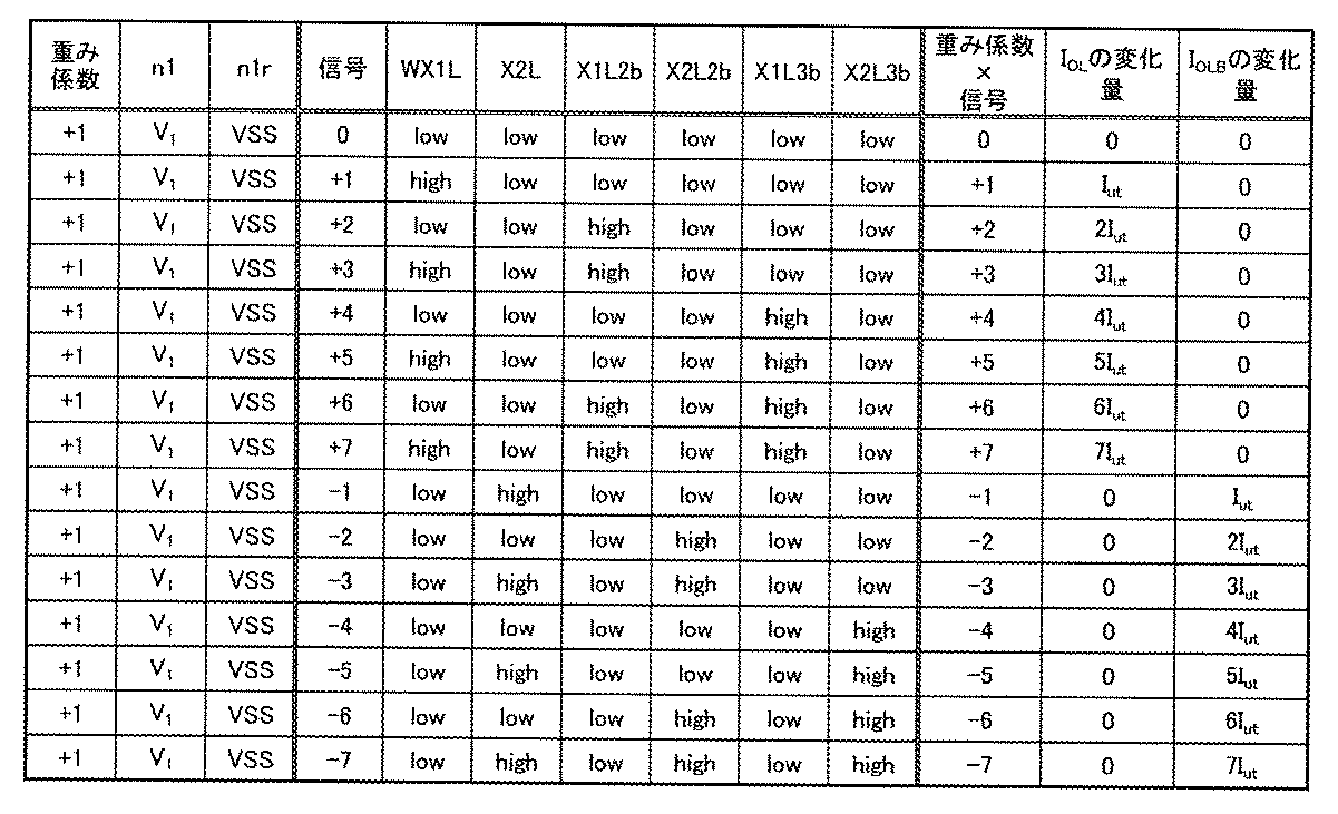

図36に示す回路MPは、複数の保持部として、回路HCS、回路HCS−2b、回路HCS−3b、回路HCSr、回路HCS−2br、回路HCS−3brを有し、かつ図35の回路MPと異なる、回路構成の一例である。
構成例1乃至構成例6では、回路MPが保持する第1データ(例えば、ここでは重み係数とする。)を、“正の多値”、“0”、“負の多値”として、第2データ(例えば、ここではニューロンの信号の値とする。)との積を計算することができる回路MPについて説明したが、本構成例では、一例として、第1データ(重み係数)が“正の多値”、“0”、“負の多値”と、第2データ(ニューロンの信号の値)が“+1”、“0”の2値と、の積を計算することができる回路MPについて説明する。

次に、回路ILDに含まれているトランジスタと、回路MPに含まれているトランジスタと、が同じ極性である場合の回路MPの構成例について説明する。
図46には、図14の演算回路170に適用できる回路BSと回路MPの一例を示している。
次に、図10Bに図示した回路MPに適用できる回路構成の例について説明する。
本実施の形態では、多値の第1データ(例えば、重み係数又はニューロンの信号の一方など)と多値の第2データ(例えば、重み係数又はニューロンの信号(演算値)の他方など)との積和演算を行うことができる半導体装置、又は当該半導体装置の動作方法について説明する。
初めに、上記実施の形態で説明した半導体装置などを用いて、多値の第1データ(例えば、重み係数又はニューロンの信号の一方など)と多値の第2データ(例えば、重み係数又はニューロンの信号(演算値)の他方など)との積和演算を行う動作方法の一例について説明する。
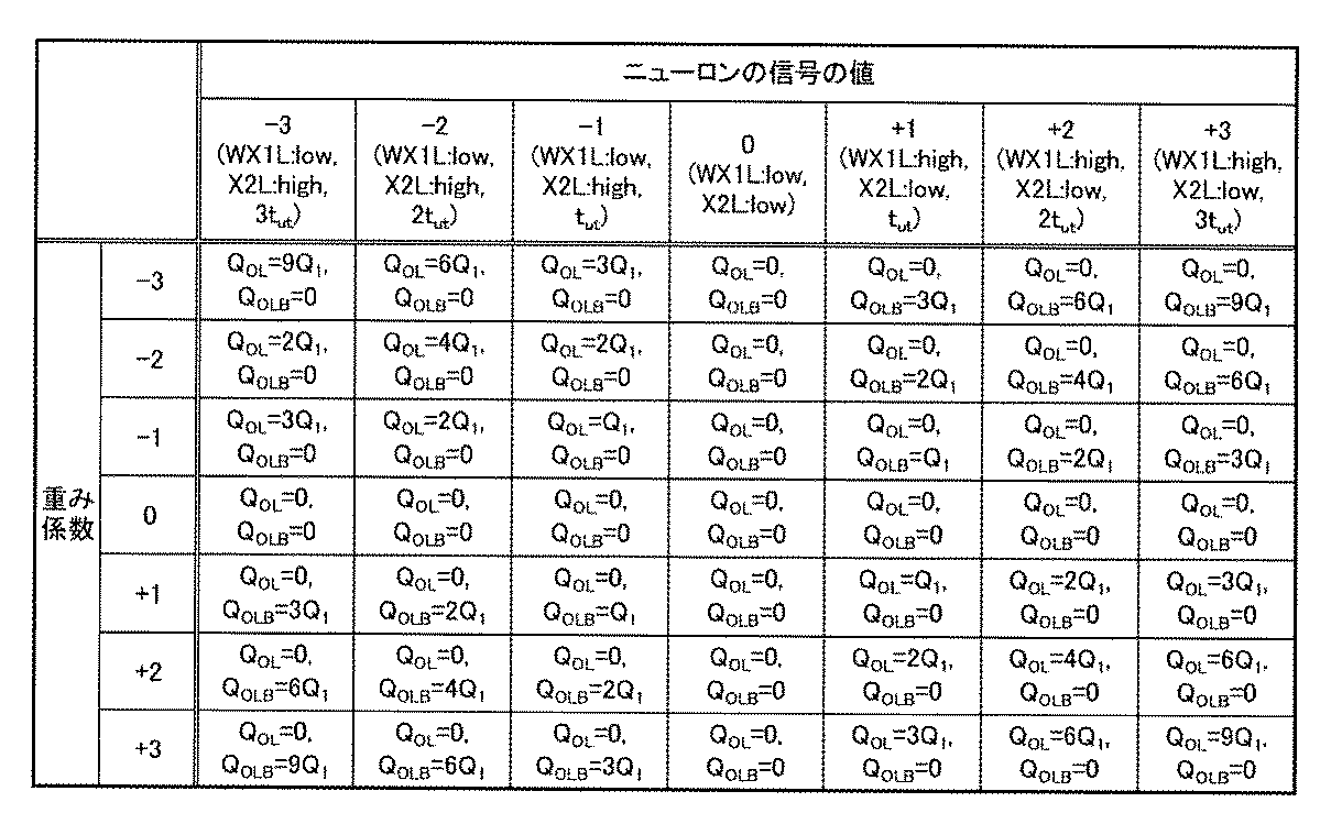
次に、図49A乃至図49Cに示した動作例とは異なる、別の動作方法の例について説明する。
ここでは、図51の回路MPを適用した図11の演算回路150の動作方法について、説明する。

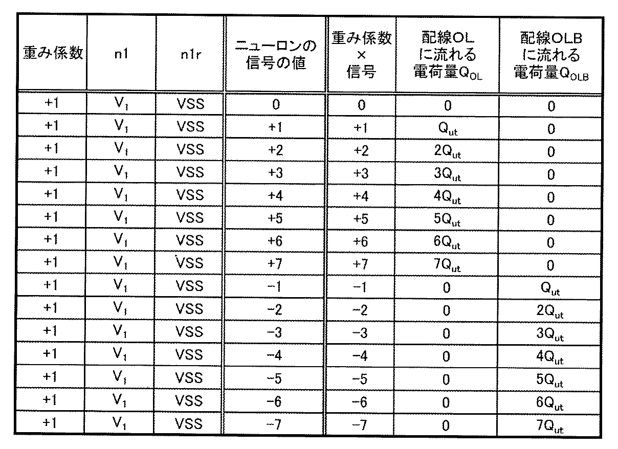
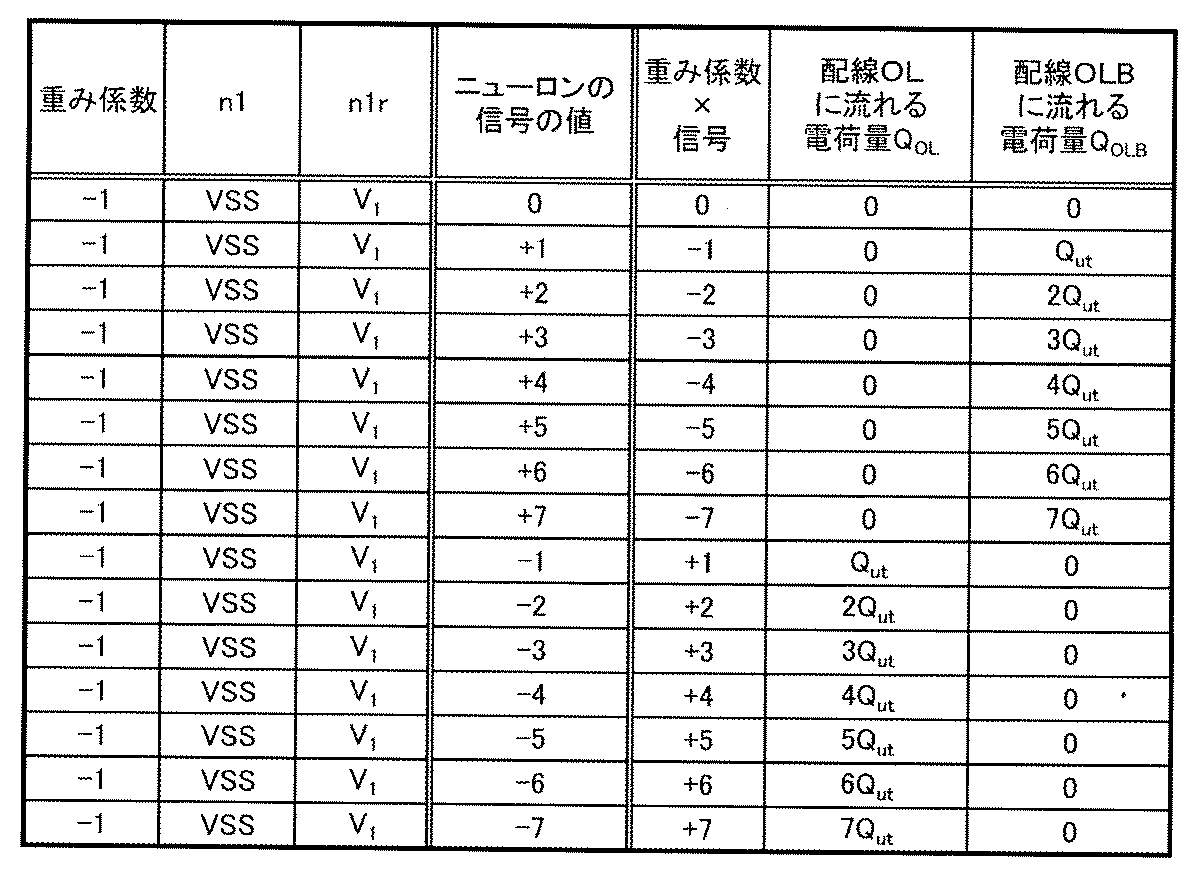
ここでは、図53の回路MPを適用した図11の演算回路150の動作方法について、説明する。
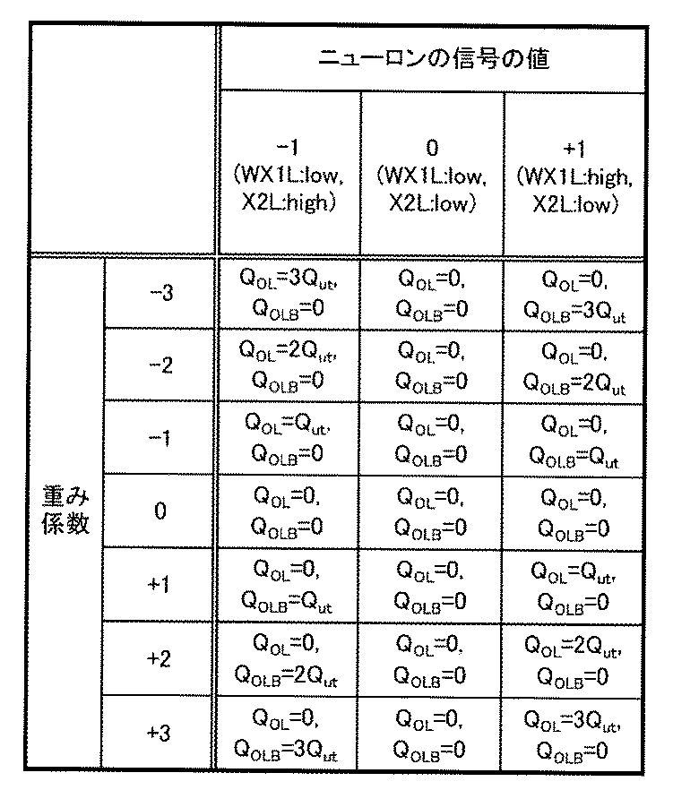
ここでは、図54の回路MPを適用した図11の演算回路150の動作方法について、説明する。


ここでは、図60Aの回路MPを適用した図3の演算回路120の動作方法について、説明する。
ここでは、図62の回路MPを適用した図11の演算回路150の動作方法について、説明する。
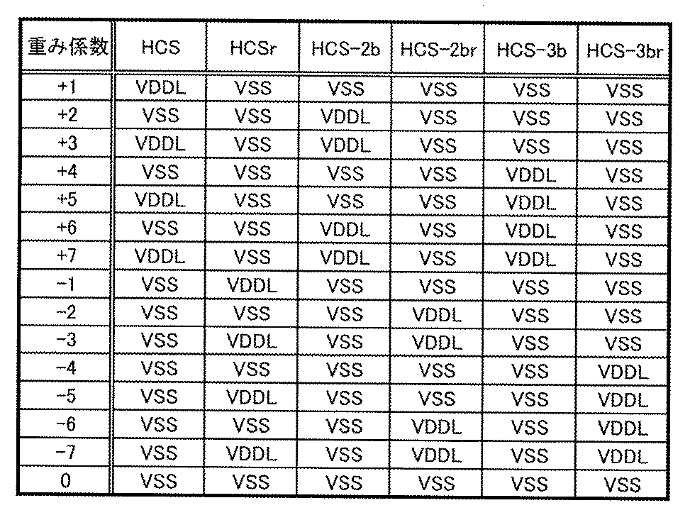
ここでは、図63の回路MPを適用した図11の演算回路150の動作方法について、説明する。


ここでは、図65の回路MPを適用した図11の演算回路150の動作方法について、説明する。


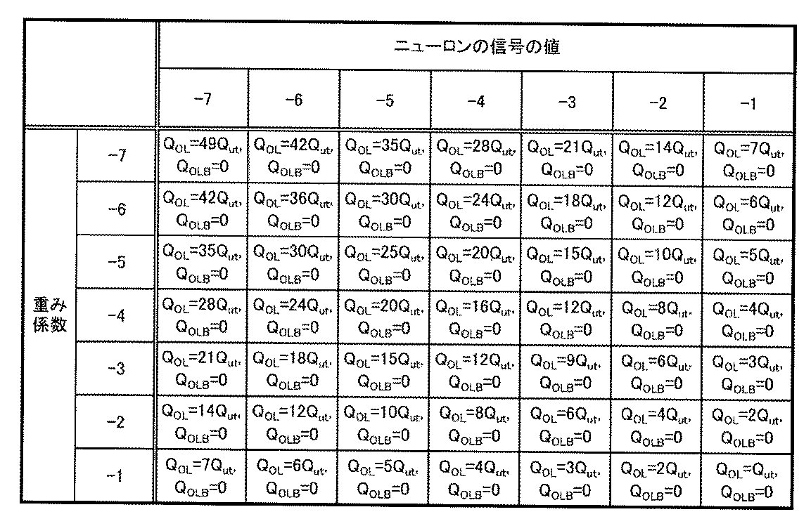
本実施の形態では、一例として、畳み込みニューラルネットワーク(CNN)で行われる演算を行うため半導体装置の構成例について説明する。なお、当該半導体装置としては、上記実施の形態で説明した半導体装置を用いることができる。
CNNは、画像などを特徴抽出する場合において使用される計算モデルの一である。図66に、CNNの構成例を示す。CNNは、畳み込み層CL、プーリング層PL、全結合層FCLなどによって構成されている。CNNは、画像データIPDが入力されることによって、画像データIPDに対する特徴抽出を行う。
次に、畳み込み層CLにおいて行われる畳み込み処理の具体例について説明する。


次に、上記の実施の形態で説明した半導体装置において、上述した畳み込み処理を行う場合について、説明する。
上記の動作例では、演算回路110を用いて畳み込み処理を行う動作について、説明したが、演算回路120、演算回路130、演算回路140、演算回路150、演算回路160、及び演算回路170を用いても、画像に対する畳み込み処理を行うことができる。
本実施の形態では、上記実施の形態で説明した半導体装置の構成例、及び上記の実施の形態で説明した半導体装置に適用できるトランジスタの構成例について説明する。
図77は、上記実施の形態で説明した半導体装置の一例であって、当該半導体装置は、トランジスタ300と、トランジスタ500と、容量素子600と、を有する。また、図78Aにはトランジスタ500のチャネル長方向の断面図、図78Bにはトランジスタ500のチャネル幅方向の断面図を示しており、図78Cにはトランジスタ300のチャネル幅方向の断面図を示している。
本実施の形態では、上記の実施の形態で説明したOSトランジスタに用いることができる金属酸化物(以下、酸化物半導体ともいう。)について説明する。
まず、酸化物半導体における、結晶構造の分類について、図82Aを用いて説明を行う。図82Aは、酸化物半導体、代表的にはIGZO(Inと、Gaと、Znと、を含む金属酸化物)の結晶構造の分類を説明する図である。
なお、酸化物半導体は、結晶構造に着目した場合、図82Aとは異なる分類となる場合がある。例えば、酸化物半導体は、単結晶酸化物半導体と、それ以外の非単結晶酸化物半導体と、に分けられる。非単結晶酸化物半導体としては、例えば、上述のCAAC−OS、及びnc−OSがある。また、非単結晶酸化物半導体には、多結晶酸化物半導体、擬似非晶質酸化物半導体(a−like OS:amorphous−like oxide semiconductor)、非晶質酸化物半導体、などが含まれる。
CAAC−OSは、複数の結晶領域を有し、当該複数の結晶領域はc軸が特定の方向に配向している酸化物半導体である。なお、特定の方向とは、CAAC−OS膜の厚さ方向、CAAC−OS膜の被形成面の法線方向、またはCAAC−OS膜の表面の法線方向である。また、結晶領域とは、原子配列に周期性を有する領域である。なお、原子配列を格子配列とみなすと、結晶領域とは、格子配列の揃った領域でもある。さらに、CAAC−OSは、a−b面方向において複数の結晶領域が連結する領域を有し、当該領域は歪みを有する場合がある。なお、歪みとは、複数の結晶領域が連結する領域において、格子配列の揃った領域と、別の格子配列の揃った領域と、の間で格子配列の向きが変化している箇所を指す。つまり、CAAC−OSは、c軸配向し、a−b面方向には明らかな配向をしていない酸化物半導体である。
nc−OSは、微小な領域(例えば、1nm以上10nm以下の領域、特に1nm以上3nm以下の領域)において原子配列に周期性を有する。別言すると、nc−OSは、微小な結晶を有する。なお、当該微小な結晶の大きさは、例えば、1nm以上10nm以下、特に1nm以上3nm以下であることから、当該微小な結晶をナノ結晶ともいう。また、nc−OSは、異なるナノ結晶間で結晶方位に規則性が見られない。そのため、膜全体で配向性が見られない。したがって、nc−OSは、分析方法によっては、a−like OS、及び非晶質酸化物半導体と区別が付かない場合がある。例えば、nc−OS膜に対し、XRD装置を用いて構造解析を行うと、θ/2θスキャンを用いたOut−of−plane XRD測定では、結晶性を示すピークが検出されない。また、nc−OS膜に対し、ナノ結晶よりも大きいプローブ径(例えば50nm以上)の電子線を用いる電子線回折(制限視野電子線回折ともいう。)を行うと、ハローパターンのような回折パターンが観測される。一方、nc−OS膜に対し、ナノ結晶の大きさと近いかナノ結晶より小さいプローブ径(例えば1nm以上30nm以下)の電子線を用いる電子線回折(ナノビーム電子線回折ともいう。)を行うと、ダイレクトスポットを中心とするリング状の領域内に複数のスポットが観測される電子線回折パターンが取得される場合がある。
a−like OSは、nc−OSと非晶質酸化物半導体との間の構造を有する酸化物半導体である。a−like OSは、鬆又は低密度領域を有する。即ち、a−like OSは、nc−OS及びCAAC−OSと比べて、結晶性が低い。また、a−like OSは、nc−OS及びCAAC−OSと比べて、膜中の水素濃度が高い。
次に、上述のCAC−OSの詳細について、説明を行う。なお、CAC−OSは材料構成に関する。
CAC−OSとは、例えば、金属酸化物を構成する元素が、0.5nm以上10nm以下、好ましくは、1nm以上3nm以下、またはその近傍のサイズで偏在した材料の一構成である。なお、以下では、金属酸化物において、一つまたは複数の金属元素が偏在し、該金属元素を有する領域が、0.5nm以上10nm以下、好ましくは、1nm以上3nm以下、またはその近傍のサイズで混合した状態をモザイク状、またはパッチ状ともいう。
続いて、上記酸化物半導体をトランジスタに用いる場合について説明する。
ここで、酸化物半導体中における各不純物の影響について説明する。
本実施の形態は、上記実施の形態に示す半導体装置などが形成された半導体ウェハ、及び当該半導体装置が組み込まれた電子部品の一例を示す。
初めに、半導体装置などが形成された半導体ウェハの例を、図83Aを用いて説明する。
図83Cに電子部品4700および電子部品4700が実装された基板(実装基板4704)の斜視図を示す。図83Cに示す電子部品4700は、モールド4711内にチップ4800aを有している。なお、図83Cに示すとおり、チップ4800aは、回路部4802が積層された構成としてもよい。図83Cは、電子部品4700の内部を示すために、一部を省略している。電子部品4700は、モールド4711の外側にランド4712を有する。ランド4712は電極パッド4713と電気的に接続され、電極パッド4713はチップ4800aとワイヤ4714によって電気的に接続されている。電子部品4700は、例えばプリント基板4702に実装される。このような電子部品が複数組み合わされて、それぞれがプリント基板4702上で電気的に接続されることで実装基板4704が完成する。
本実施の形態では、上記実施の形態で説明した半導体装置を有する電子機器の一例について説明する。なお、図84には、当該半導体装置を有する電子部品4700が各電子機器に含まれている様子を図示している。
図84に示す情報端末5500は、情報端末の一種である携帯電話(スマートフォン)である。情報端末5500は、筐体5510と、表示部5511と、を有しており、入力用インターフェースとして、タッチパネルが表示部5511に備えられ、ボタンが筐体5510に備えられている。
また、図84には、ウェアラブル端末の一例として腕時計型の情報端末5900が図示されている。情報端末5900は、筐体5901、表示部5902、操作ボタン5903、操作子5904、バンド5905などを有する。
また、図84には、デスクトップ型情報端末5300が図示されている。デスクトップ型情報端末5300は、情報端末の本体5301と、ディスプレイ5302と、キーボード5303と、を有する。
また、図84には、電化製品の一例として電気冷凍冷蔵庫5800が図示されている。電気冷凍冷蔵庫5800は、筐体5801、冷蔵室用扉5802、冷凍室用扉5803等を有する。
また、図84には、ゲーム機の一例である携帯ゲーム機5200が図示されている。携帯ゲーム機5200は、筐体5201、表示部5202、ボタン5203等を有する。
上記実施の形態で説明した半導体装置は、移動体である自動車、及び自動車の運転席周辺に適用することができる。
上記実施の形態で説明した半導体装置は、カメラに適用することができる。
上記実施の形態で説明した半導体装置は、ビデオカメラに適用することができる。
上記実施の形態で説明した半導体装置は、PC(Personal Computer)などの計算機、情報端末用の拡張デバイスに適用することができる。
上記実施の形態で説明した半導体装置は、放送システムに適用することができる。
上記実施の形態で説明した半導体装置は、認証システムに適用することができる。
Claims (9)
- 第1回路と、第2回路と、を有し、
前記第1回路は、第1保持部と、第1駆動トランジスタと、を有し、
前記第2回路は、第2保持部と、第2駆動トランジスタと、を有し、
前記第1回路は、第1入力配線と、第2入力配線と、第1配線と、第2配線と、に電気的に接続され、
前記第2回路は、前記第1入力配線と、前記第2入力配線と、前記第1配線と、前記第2配線と、に電気的に接続され、
前記第1保持部は、前記第1配線から前記第1駆動トランジスタのソース−ドレイン間に流れる第1電流に応じた第1電位を保持する機能を有し、
前記第2保持部は、前記第2配線から前記第2駆動トランジスタのソース−ドレイン間に流れる第2電流に応じた第2電位を保持する機能を有し、
前記第1回路は、
前記第1入力配線に第1レベル電位が入力され、かつ前記第2入力配線に第2レベル電位が入力されたときに、前記第1電流を前記第1配線に出力する機能と、
前記第1入力配線に前記第2レベル電位が入力され、かつ前記第2入力配線に前記第1レベル電位が入力されたときに、前記第1電流を前記第2配線に出力する機能と、
前記第1入力配線に前記第2レベル電位が入力され、かつ前記第2入力配線に前記第2レベル電位が入力されたときに、前記第1電流を前記第1配線、及び前記第2配線に出力しない機能と、を有し、
前記第2回路は、
前記第1入力配線に前記第1レベル電位が入力され、かつ前記第2入力配線に前記第2レベル電位が入力されたときに、前記第2電流を前記第2配線に出力する機能と、
前記第1入力配線に前記第2レベル電位が入力され、かつ前記第2入力配線に前記第1レベル電位が入力されたときに、前記第2電流を前記第1配線に出力する機能と、
前記第1入力配線に前記第2レベル電位が入力され、かつ前記第2入力配線に前記第2レベル電位が入力されたときに、前記第2電流を前記第1配線、及び前記第2配線に出力しない機能と、を有し、
前記第1電流と、前記第2電流と、のそれぞれの電流量は、畳み込み処理に用いられるフィルタに含まれるフィルタ値に応じた量であり、
前記第1入力配線と、前記第2入力配線と、のそれぞれに入力される前記第1レベル電位、及び前記第2レベル電位は、前記畳み込み処理が施される画像データに応じて決められる、
半導体装置。 - 第1回路と、第2回路と、を有し、
前記第1回路は、第1保持部と、第1駆動トランジスタと、を有し、
前記第2回路は、第2保持部と、第2駆動トランジスタと、を有し、
前記第1回路は、第1入力配線と、第2入力配線と、第1配線と、第2配線と、に電気的に接続され、
前記第2回路は、前記第1入力配線と、前記第2入力配線と、前記第1配線と、前記第2配線と、に電気的に接続され、
前記第1保持部は、前記第1配線から前記第1駆動トランジスタのソース−ドレイン間に流れる第1電流に応じた第1電位を保持する機能を有し、
前記第2保持部は、前記第2配線から前記第2駆動トランジスタのソース−ドレイン間に流れる第2電流に応じた第2電位を保持する機能を有し、
前記第1駆動トランジスタは、前記第1駆動トランジスタのソース−ドレイン間において、保持された前記第1電位に応じた前記第1電流を流す機能を有し、
前記第2駆動トランジスタは、前記第2駆動トランジスタのソース−ドレイン間において、保持された前記第2電位に応じた前記第2電流を流す機能を有し、
前記第1回路は、
第1期間に、前記第1入力配線に第1レベル電位が入力され、かつ前記第2入力配線に第2レベル電位が入力されたときに、前記第1電流を前記第1配線に出力する機能と、
前記第1期間に、前記第1入力配線に前記第2レベル電位が入力され、かつ前記第2入力配線に前記第1レベル電位が入力されたときに、前記第1電流を前記第2配線に出力する機能と、
前記第1期間に、前記第1入力配線に前記第2レベル電位が入力され、かつ前記第2入力配線に前記第2レベル電位が入力されたときに、前記第1電流を前記第1配線、及び前記第2配線に出力しない機能と、を有し、
前記第2回路は、
前記第1期間に、前記第1入力配線に前記第1レベル電位が入力され、かつ前記第2入力配線に前記第2レベル電位が入力されたときに、前記第2電流を前記第2配線に出力する機能と、
前記第1期間に、前記第1入力配線に前記第2レベル電位が入力され、かつ前記第2入力配線に前記第1レベル電位が入力されたときに、前記第2電流を前記第1配線に出力する機能と、
前記第1期間に、前記第1入力配線に前記第2レベル電位が入力され、かつ前記第2入力配線に前記第2レベル電位が入力されたときに、前記第2電流を前記第1配線、及び前記第2配線に出力しない機能と、を有し、
前記第1電流と、前記第2電流と、のそれぞれの電流量は、畳み込み処理に用いられるフィルタに含まれるフィルタ値に応じた量であり、
前記第1入力配線と、前記第2入力配線と、のそれぞれに入力される前記第1レベル電位、及び前記第2レベル電位と、前記第1期間の長さと、は、前記畳み込み処理が施される画像データに応じて決められる、
半導体装置。 - 請求項2において、
前記第1期間は、第2期間と、第3期間と、を有し、
前記第1入力配線は、前記第2期間において、前記第1回路及び前記第2回路の両方に前記第1レベル電位又は前記第2レベル電位を与える機能を有し、
前記第2入力配線は、前記第2期間において、前記第1回路及び前記第2回路の両方に前記第1レベル電位又は前記第2レベル電位を与える機能を有し、
前記第1入力配線は、前記第3期間において、前記第1回路及び前記第2回路の両方に前記第1レベル電位又は前記第2レベル電位を与える機能を有し、
前記第2入力配線は、前記第3期間において、前記第1回路及び前記第2回路の両方に前記第1レベル電位又は前記第2レベル電位を与える出力する機能を有し、
前記第3期間の長さは、前記第2期間の長さの1.8倍以上2.2倍以下である、
半導体装置。 - 請求項1乃至請求項3のいずれか一において、
前記第1回路は、第1トランジスタと、第2トランジスタと、第3トランジスタと、第1容量と、を有し、
前記第2回路は、第4トランジスタと、第5トランジスタと、第6トランジスタと、第2容量と、を有し、
前記第1保持部は、前記第1トランジスタと、前記第1容量と、を有し、
前記第2保持部は、前記第4トランジスタと、前記第2容量と、を有し、
前記第1トランジスタの第1端子は、前記第1容量の第1端子と、前記第1駆動トランジスタのゲートに電気的に接続され、
前記第1トランジスタの第2端子は、前記第1配線に電気的に接続され、
前記第1駆動トランジスタの第1端子は、前記第2トランジスタの第1端子と、前記第3トランジスタの第1端子と、に電気的に接続され、
前記第2トランジスタの第2端子は、前記第1配線に電気的に接続され、
前記第2トランジスタのゲートは、前記第1入力配線に電気的に接続され、
前記第3トランジスタの第2端子は、前記第2配線に電気的に接続され、
前記第3トランジスタのゲートは、前記第2入力配線に電気的に接続され、
前記第4トランジスタの第1端子は、前記第2容量の第1端子と、前記第2駆動トランジスタのゲートに電気的に接続され、
前記第4トランジスタの第2端子は、前記第2配線に電気的に接続され、
前記第2駆動トランジスタの第1端子は、前記第5トランジスタの第1端子と、前記第6トランジスタの第1端子と、に電気的に接続され、
前記第5トランジスタの第2端子は、前記第2配線に電気的に接続され、
前記第5トランジスタのゲートは、前記第1入力配線に電気的に接続され、
前記第6トランジスタの第2端子は、前記第1配線に電気的に接続され、
前記第6トランジスタのゲートは、前記第2入力配線に電気的に接続されている、
半導体装置。 - 請求項4において、
前記第1回路は、第7トランジスタを有し、
前記第2回路は、第8トランジスタを有し、
前記第7トランジスタの第1端子は、前記第1駆動トランジスタの第1端子と、前記第2トランジスタの第1端子と、前記第3トランジスタの第1端子と、に電気的に接続され、
前記第7トランジスタの第2端子は、前記第1トランジスタの第1端子、又は第2端子の一方に電気的に接続され、
前記第8トランジスタの第1端子は、前記第2駆動トランジスタの第1端子と、前記第5トランジスタの第1端子と、前記第6トランジスタの第1端子と、に電気的に接続され、
前記第8トランジスタの第2端子は、前記第4トランジスタの第1端子、又は第2端子の一方に電気的に接続され、
前記第1トランジスタのゲートは、前記第4トランジスタのゲートと、前記第7トランジスタのゲートと、前記第8トランジスタのゲートと、に電気的に接続されている、
半導体装置。 - 請求項1乃至請求項3のいずれか一において、
前記第1回路は、第1トランジスタと、第2トランジスタと、第3トランジスタと、第1容量と、を有し、
前記第2回路は、第4トランジスタと、第5トランジスタと、第6トランジスタと、第2容量と、を有し、
前記第1保持部は、前記第1トランジスタと、前記第1容量と、を有し、
前記第2保持部は、前記第4トランジスタと、前記第2容量と、を有し、
前記第1トランジスタの第1端子は、前記第1容量の第1端子と、前記第1駆動トランジスタのゲートと、に電気的に接続され、
前記第1駆動トランジスタの第1端子は、前記第1トランジスタの第2端子と、前記第2トランジスタの第1端子と、前記第3トランジスタの第1端子と、に電気的に接続され、
前記第2トランジスタの第2端子は、前記第1配線に電気的に接続され、
前記第2トランジスタのゲートは、前記第1入力配線に電気的に接続され、
前記第3トランジスタの第2端子は、前記第2配線に電気的に接続され、
前記第3トランジスタのゲートは、前記第2入力配線に電気的に接続され、
前記第4トランジスタの第1端子は、前記第2容量の第1端子と、前記第2駆動トランジスタのゲートに電気的に接続され、
前記第2駆動トランジスタの第1端子は、前記第4トランジスタの第2端子と、前記第5トランジスタの第1端子と、前記第6トランジスタの第1端子と、に電気的に接続され、
前記第5トランジスタの第2端子は、前記第2配線に電気的に接続され、
前記第5トランジスタのゲートは、前記第1入力配線に電気的に接続され、
前記第6トランジスタの第2端子は、前記第1配線に電気的に接続され、
前記第6トランジスタのゲートは、前記第2入力配線に電気的に接続されている、
半導体装置。 - 請求項1乃至請求項3のいずれか一において、
前記第1回路は、第3保持部と、第3駆動トランジスタと、を有し、
前記第2回路は、第4保持部と、第4駆動トランジスタと、を有し、
前記第1回路は、第3配線に電気的に接続され、
前記第2回路は、前記第3配線に電気的に接続され、
前記第3保持部は、前記第1配線から前記第3駆動トランジスタのソース−ドレイン間に流れる第3電流に応じた第3電位を保持する機能を有し、
前記第4保持部は、前記第2配線から前記第4駆動トランジスタのソース−ドレイン間に流れる第4電流に応じた第4電位を保持する機能を有し、
前記第3駆動トランジスタは、前記第3駆動トランジスタのソース−ドレイン間において、保持された前記第3電位に応じた前記第3電流を流す機能を有し、
前記第4駆動トランジスタは、前記第4駆動トランジスタのソース−ドレイン間において、保持された前記第4電位に応じた前記第4電流を流す機能を有し、
前記第3配線に入力される信号に応じて、前記第1配線又は前記第2配線の一方に流れる前記第1電流を前記第3電流に切り替え、かつ前記第1配線又は前記第2配線の他方に流れる前記第2電流を前記第4電流に切り替える機能を有する、
半導体装置。 - 請求項1乃至請求項7のいずれか一において、
第3回路と、第4回路と、第5回路と、を有し、
前記第3回路は、
前記第1配線を介して、前記第1回路に、前記フィルタ値に応じた前記第1電流を供給する機能と、
前記第2配線を介して、前記第2回路に、前記フィルタ値に応じた前記第2電流を供給する機能と、
前記第4回路は、
前記画像データに応じて、前記第1入力配線に、前記第1レベル電位又は前記第2レベル電位を入力する機能と、
前記画像データに応じて、前記第2入力配線に、前記第1レベル電位又は前記第2レベル電位を入力する機能と、
を有し、
前記第5回路は、前記第1配線と、前記第2配線と、のそれぞれから流れる電流を比較して、前記第5回路の出力端子から、前記フィルタ値と前記画像データの積に応じた電位を出力する機能を有する半導体装置。 - 請求項1乃至請求項8のいずれか一の半導体装置と、筐体と、を有し、
前記畳み込み処理によって、画像の特徴抽出が行われる電子機器。
Priority Applications (6)
| Application Number | Priority Date | Filing Date | Title |
|---|---|---|---|
| KR1020237003390A KR20230041718A (ko) | 2020-07-17 | 2021-07-06 | 반도체 장치 및 전자 기기 |
| JP2022535982A JP7614204B2 (ja) | 2020-07-17 | 2021-07-06 | 半導体装置、及び電子機器 |
| US18/011,712 US12243583B2 (en) | 2020-07-17 | 2021-07-06 | Semiconductor device electronic device |
| CN202180049274.8A CN115836293A (zh) | 2020-07-17 | 2021-07-06 | 半导体装置及电子设备 |
| JP2024230233A JP2025060890A (ja) | 2020-07-17 | 2024-12-26 | 半導体装置 |
| US19/028,268 US20250166697A1 (en) | 2020-07-17 | 2025-01-17 | Semiconductor device electronic device |
Applications Claiming Priority (2)
| Application Number | Priority Date | Filing Date | Title |
|---|---|---|---|
| JP2020122594 | 2020-07-17 | ||
| JP2020-122594 | 2020-07-17 |
Related Child Applications (2)
| Application Number | Title | Priority Date | Filing Date |
|---|---|---|---|
| US18/011,712 A-371-Of-International US12243583B2 (en) | 2020-07-17 | 2021-07-06 | Semiconductor device electronic device |
| US19/028,268 Continuation US20250166697A1 (en) | 2020-07-17 | 2025-01-17 | Semiconductor device electronic device |
Publications (1)
| Publication Number | Publication Date |
|---|---|
| WO2022013680A1 true WO2022013680A1 (ja) | 2022-01-20 |
Family
ID=79554314
Family Applications (1)
| Application Number | Title | Priority Date | Filing Date |
|---|---|---|---|
| PCT/IB2021/056024 Ceased WO2022013680A1 (ja) | 2020-07-17 | 2021-07-06 | 半導体装置、及び電子機器 |
Country Status (5)
| Country | Link |
|---|---|
| US (2) | US12243583B2 (ja) |
| JP (2) | JP7614204B2 (ja) |
| KR (1) | KR20230041718A (ja) |
| CN (1) | CN115836293A (ja) |
| WO (1) | WO2022013680A1 (ja) |
Cited By (2)
| Publication number | Priority date | Publication date | Assignee | Title |
|---|---|---|---|---|
| US12033694B2 (en) | 2020-07-17 | 2024-07-09 | Semiconductor Energy Laboratory Co., Ltd. | Semiconductor device and electronic device |
| US12475361B2 (en) | 2019-05-17 | 2025-11-18 | Semiconductor Energy Laboratory Co., Ltd. | Semiconductor device and electronic device |
Families Citing this family (1)
| Publication number | Priority date | Publication date | Assignee | Title |
|---|---|---|---|---|
| US12481867B2 (en) * | 2021-04-28 | 2025-11-25 | Arm Limited | Memory for artificial neural network accelerator |
Citations (2)
| Publication number | Priority date | Publication date | Assignee | Title |
|---|---|---|---|---|
| JP2018109968A (ja) * | 2016-12-28 | 2018-07-12 | 株式会社半導体エネルギー研究所 | ニューラルネットワークを利用したデータ処理装置、電子部品、および電子機器 |
| JP2019003464A (ja) * | 2017-06-16 | 2019-01-10 | 株式会社半導体エネルギー研究所 | 半導体装置、演算回路及び電子機器 |
Family Cites Families (20)
| Publication number | Priority date | Publication date | Assignee | Title |
|---|---|---|---|---|
| US6462584B1 (en) * | 1999-02-13 | 2002-10-08 | Integrated Device Technology, Inc. | Generating a tail current for a differential transistor pair using a capacitive device to project a current flowing through a current source device onto a node having a different voltage than the current source device |
| US6462998B1 (en) * | 1999-02-13 | 2002-10-08 | Integrated Device Technology, Inc. | Programmable and electrically configurable latch timing circuit |
| KR20170001788A (ko) * | 2015-06-25 | 2017-01-05 | 삼성디스플레이 주식회사 | 표시 장치 및 표시 패널 구동 방법 |
| KR102410029B1 (ko) * | 2015-08-24 | 2022-06-20 | 삼성디스플레이 주식회사 | 영상 처리 회로 및 이를 포함하는 표시 장치 |
| US9747514B2 (en) * | 2015-08-31 | 2017-08-29 | Apple Inc. | Noise filtering and image sharpening utilizing common spatial support |
| US10565500B2 (en) * | 2016-12-20 | 2020-02-18 | Intel Corporation | Unsupervised learning using neuromorphic computing |
| US20180240392A1 (en) * | 2017-02-21 | 2018-08-23 | Solomon Systech Limited | Thin film transistor (tft) liquid crystal display (lcd) panel |
| JP6990520B2 (ja) * | 2017-03-30 | 2022-01-12 | パナソニック液晶ディスプレイ株式会社 | 液晶表示装置 |
| JP6854686B2 (ja) * | 2017-04-04 | 2021-04-07 | 株式会社半導体エネルギー研究所 | 半導体装置、及び電子機器 |
| US11195079B2 (en) * | 2017-11-22 | 2021-12-07 | Intel Corporation | Reconfigurable neuro-synaptic cores for spiking neural network |
| US11593623B2 (en) * | 2017-12-22 | 2023-02-28 | Intel Corporation | Spiking neural network accelerator using external memory |
| US20190042915A1 (en) * | 2018-03-30 | 2019-02-07 | Intel Corporation | Procedural neural network synaptic connection modes |
| US20200012924A1 (en) * | 2018-07-03 | 2020-01-09 | Sandisk Technologies Llc | Pipelining to improve neural network inference accuracy |
| TWI715068B (zh) * | 2018-07-17 | 2021-01-01 | 日商索尼股份有限公司 | 運算裝置、積和運算裝置、積和運算電路及積和運算系統 |
| JP6789576B2 (ja) * | 2018-08-02 | 2020-11-25 | 株式会社フローディア | 積和演算装置 |
| US12453072B2 (en) * | 2018-11-08 | 2025-10-21 | Semiconductor Energy Laboratory Co., Ltd. | Semiconductor device that can perform product-sum operation with low power consumption |
| US11074318B2 (en) * | 2018-12-14 | 2021-07-27 | Western Digital Technologies, Inc. | Hardware accelerated discretized neural network |
| US11074877B1 (en) * | 2020-01-23 | 2021-07-27 | Panasonic Liquid Crystal Display Co., Ltd. | Multi-panel liquid crystal display device and method for displaying image therein |
| US12050997B2 (en) * | 2020-05-27 | 2024-07-30 | International Business Machines Corporation | Row-by-row convolutional neural network mapping for analog artificial intelligence network training |
| KR20240003041A (ko) * | 2022-06-29 | 2024-01-08 | 삼성디스플레이 주식회사 | 표시 장치 및 이의 구동 방법 |
-
2021
- 2021-07-06 JP JP2022535982A patent/JP7614204B2/ja active Active
- 2021-07-06 CN CN202180049274.8A patent/CN115836293A/zh active Pending
- 2021-07-06 KR KR1020237003390A patent/KR20230041718A/ko active Pending
- 2021-07-06 WO PCT/IB2021/056024 patent/WO2022013680A1/ja not_active Ceased
- 2021-07-06 US US18/011,712 patent/US12243583B2/en active Active
-
2024
- 2024-12-26 JP JP2024230233A patent/JP2025060890A/ja active Pending
-
2025
- 2025-01-17 US US19/028,268 patent/US20250166697A1/en active Pending
Patent Citations (2)
| Publication number | Priority date | Publication date | Assignee | Title |
|---|---|---|---|---|
| JP2018109968A (ja) * | 2016-12-28 | 2018-07-12 | 株式会社半導体エネルギー研究所 | ニューラルネットワークを利用したデータ処理装置、電子部品、および電子機器 |
| JP2019003464A (ja) * | 2017-06-16 | 2019-01-10 | 株式会社半導体エネルギー研究所 | 半導体装置、演算回路及び電子機器 |
Cited By (2)
| Publication number | Priority date | Publication date | Assignee | Title |
|---|---|---|---|---|
| US12475361B2 (en) | 2019-05-17 | 2025-11-18 | Semiconductor Energy Laboratory Co., Ltd. | Semiconductor device and electronic device |
| US12033694B2 (en) | 2020-07-17 | 2024-07-09 | Semiconductor Energy Laboratory Co., Ltd. | Semiconductor device and electronic device |
Also Published As
| Publication number | Publication date |
|---|---|
| JP2025060890A (ja) | 2025-04-10 |
| US12243583B2 (en) | 2025-03-04 |
| US20230253034A1 (en) | 2023-08-10 |
| CN115836293A (zh) | 2023-03-21 |
| JPWO2022013680A1 (ja) | 2022-01-20 |
| JP7614204B2 (ja) | 2025-01-15 |
| KR20230041718A (ko) | 2023-03-24 |
| US20250166697A1 (en) | 2025-05-22 |
Similar Documents
| Publication | Publication Date | Title |
|---|---|---|
| JP7671888B2 (ja) | 半導体装置 | |
| JP7602596B2 (ja) | 半導体装置及び電子機器 | |
| JP7854547B2 (ja) | 半導体装置 | |
| JP7811676B2 (ja) | 半導体装置 | |
| JP7661571B2 (ja) | 半導体装置および電子機器 | |
| JP7595057B2 (ja) | 半導体装置、及び電子機器 | |
| JP2025060890A (ja) | 半導体装置 | |
| WO2021229373A1 (ja) | 半導体装置、及び電子機器 | |
| JP7596386B2 (ja) | 半導体装置、及び電子機器 |
Legal Events
| Date | Code | Title | Description |
|---|---|---|---|
| 121 | Ep: the epo has been informed by wipo that ep was designated in this application |
Ref document number: 21842168 Country of ref document: EP Kind code of ref document: A1 |
|
| ENP | Entry into the national phase |
Ref document number: 2022535982 Country of ref document: JP Kind code of ref document: A |
|
| ENP | Entry into the national phase |
Ref document number: 20237003390 Country of ref document: KR Kind code of ref document: A |
|
| NENP | Non-entry into the national phase |
Ref country code: DE |
|
| 122 | Ep: pct application non-entry in european phase |
Ref document number: 21842168 Country of ref document: EP Kind code of ref document: A1 |
|
| WWG | Wipo information: grant in national office |
Ref document number: 18011712 Country of ref document: US |