WO2022009720A1 - 固体撮像装置、撮像方法および電子機器 - Google Patents
固体撮像装置、撮像方法および電子機器 Download PDFInfo
- Publication number
- WO2022009720A1 WO2022009720A1 PCT/JP2021/024364 JP2021024364W WO2022009720A1 WO 2022009720 A1 WO2022009720 A1 WO 2022009720A1 JP 2021024364 W JP2021024364 W JP 2021024364W WO 2022009720 A1 WO2022009720 A1 WO 2022009720A1
- Authority
- WO
- WIPO (PCT)
- Prior art keywords
- voltage
- input end
- amplifier
- gain
- comparator
- Prior art date
- Legal status (The legal status is an assumption and is not a legal conclusion. Google has not performed a legal analysis and makes no representation as to the accuracy of the status listed.)
- Ceased
Links
Images












Classifications
-
- H—ELECTRICITY
- H04—ELECTRIC COMMUNICATION TECHNIQUE
- H04N—PICTORIAL COMMUNICATION, e.g. TELEVISION
- H04N25/00—Circuitry of solid-state image sensors [SSIS]; Control thereof
- H04N25/50—Control of the SSIS exposure
- H04N25/57—Control of the dynamic range
-
- H—ELECTRICITY
- H03—ELECTRONIC CIRCUITRY
- H03F—AMPLIFIERS
- H03F3/00—Amplifiers with only discharge tubes or only semiconductor devices as amplifying elements
- H03F3/04—Amplifiers with only discharge tubes or only semiconductor devices as amplifying elements with semiconductor devices only
- H03F3/08—Amplifiers with only discharge tubes or only semiconductor devices as amplifying elements with semiconductor devices only controlled by light
- H03F3/082—Amplifiers with only discharge tubes or only semiconductor devices as amplifying elements with semiconductor devices only controlled by light with FET's
-
- H—ELECTRICITY
- H03—ELECTRONIC CIRCUITRY
- H03F—AMPLIFIERS
- H03F3/00—Amplifiers with only discharge tubes or only semiconductor devices as amplifying elements
- H03F3/45—Differential amplifiers
- H03F3/45071—Differential amplifiers with semiconductor devices only
- H03F3/45076—Differential amplifiers with semiconductor devices only characterised by the way of implementation of the active amplifying circuit in the differential amplifier
- H03F3/45475—Differential amplifiers with semiconductor devices only characterised by the way of implementation of the active amplifying circuit in the differential amplifier using IC blocks as the active amplifying circuit
-
- H—ELECTRICITY
- H03—ELECTRONIC CIRCUITRY
- H03G—CONTROL OF AMPLIFICATION
- H03G3/00—Gain control in amplifiers or frequency changers
- H03G3/20—Automatic control
- H03G3/30—Automatic control in amplifiers having semiconductor devices
-
- H—ELECTRICITY
- H04—ELECTRIC COMMUNICATION TECHNIQUE
- H04N—PICTORIAL COMMUNICATION, e.g. TELEVISION
- H04N25/00—Circuitry of solid-state image sensors [SSIS]; Control thereof
- H04N25/47—Image sensors with pixel address output; Event-driven image sensors; Selection of pixels to be read out based on image data
-
- H—ELECTRICITY
- H04—ELECTRIC COMMUNICATION TECHNIQUE
- H04N—PICTORIAL COMMUNICATION, e.g. TELEVISION
- H04N25/00—Circuitry of solid-state image sensors [SSIS]; Control thereof
- H04N25/50—Control of the SSIS exposure
- H04N25/51—Control of the gain
-
- H—ELECTRICITY
- H04—ELECTRIC COMMUNICATION TECHNIQUE
- H04N—PICTORIAL COMMUNICATION, e.g. TELEVISION
- H04N25/00—Circuitry of solid-state image sensors [SSIS]; Control thereof
- H04N25/70—SSIS architectures; Circuits associated therewith
- H04N25/76—Addressed sensors, e.g. MOS or CMOS sensors
- H04N25/77—Pixel circuitry, e.g. memories, A/D converters, pixel amplifiers, shared circuits or shared components
- H04N25/778—Pixel circuitry, e.g. memories, A/D converters, pixel amplifiers, shared circuits or shared components comprising amplifiers shared between a plurality of pixels, i.e. at least one part of the amplifier must be on the sensor array itself
-
- H—ELECTRICITY
- H04—ELECTRIC COMMUNICATION TECHNIQUE
- H04N—PICTORIAL COMMUNICATION, e.g. TELEVISION
- H04N25/00—Circuitry of solid-state image sensors [SSIS]; Control thereof
- H04N25/70—SSIS architectures; Circuits associated therewith
- H04N25/76—Addressed sensors, e.g. MOS or CMOS sensors
- H04N25/78—Readout circuits for addressed sensors, e.g. output amplifiers or A/D converters
-
- H—ELECTRICITY
- H03—ELECTRONIC CIRCUITRY
- H03G—CONTROL OF AMPLIFICATION
- H03G2201/00—Indexing scheme relating to subclass H03G
- H03G2201/10—Gain control characterised by the type of controlled element
- H03G2201/103—Gain control characterised by the type of controlled element being an amplifying element
Definitions
- the present disclosure relates to a solid-state image sensor, an image pickup method, and an electronic device.
- CMOS Complementary Metal Oxide Semiconductor
- a detection circuit is provided for each pixel address to detect in real time that the amount of light received by the pixel exceeds the threshold value as an address event.
- Asynchronous solid-state image sensors are known.
- Such a solid-state image sensor that detects an address event for each pixel is called a DVS (Dynamic Vision Sensor).
- the photocurrent output from the photoelectric conversion element is converted into a logarithmic voltage signal, and this voltage signal is compared with a threshold value by a comparator to detect an address event. ..
- the contrast sensitivity of the DVS can be adjusted by controlling the threshold value in the comparator.
- the contrast sensitivity in DVS, for example, in order to widen the dynamic range, it may be desired to lower the contrast sensitivity. As described above, it is possible to lower the contrast sensitivity by controlling the threshold value for the comparator. However, if the gain of the comparator itself is high, the control range of the contrast sensitivity is limited to the voltage range in which the threshold value can be set.
- the solid-state imaging device has a generation unit that generates a voltage corresponding to the logarithmic value of the photocurrent, a capacitor in which the voltage generated by the generation unit is applied to the first electrode, and a first input end.
- the second electrode of the capacitor was connected, the first reference voltage was applied to the second input end, and the voltage applied to the first input end and the voltage applied to the second input end were compared.
- the first amplifier that outputs the comparison result, the switch unit that controls the connection between the output of the first amplifier and the first input end, and the output of the first amplifier are connected to the third input end.
- a second amplifier that outputs a comparison result in which a second reference voltage is applied to the fourth input end and the voltage applied to the third input end is compared with the voltage applied to the fourth input end.
- the first gain of the first amplifier is lower than the second gain of the second amplifier.
- FIG. 1 is a block diagram showing a configuration of an example of an image pickup device as an electronic device applicable to each embodiment.
- the image pickup device 100 includes an optical unit 110, a solid-state image pickup element 200, a recording unit 120, and a control unit 130.
- the image pickup apparatus 100 a camera mounted on an industrial robot, an in-vehicle camera, or the like is assumed.
- the optical unit 110 collects the incident light and guides it to the solid-state image sensor 200.
- the solid-state image sensor 200 performs an image pickup operation that photoelectrically converts incident light and outputs a pixel signal.
- the solid-state image sensor 200 generates output data by performing predetermined signal processing such as image recognition processing based on a pixel signal based on incident light, and supplies the generated output data to the recording unit 120 via a signal line 209. ..
- the recording unit 120 records the output data supplied from the solid-state image sensor 200.
- the control unit 130 controls the image pickup operation of the solid-state image pickup device 200 and the recording operation of the recording unit 120 according to, for example, a predetermined program.
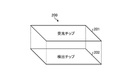
- FIG. 2 is a schematic diagram showing an example of the structure of the solid-state image sensor 200 applicable to each embodiment.
- the solid-state image pickup device 200 has a laminated structure consisting of a detection chip 202 and a light receiving chip 201 laminated on the detection chip 202.
- the light receiving chip 201 and the detection chip 202 are electrically connected via a connection portion such as a via.
- the connection method between the light receiving chip 201 and the detection chip 202 is not limited to vias, and Cu—Cu bonding or bumps can also be applied.
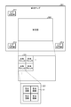
- FIG. 3 is a plan view of an example of the light receiving chip 201 applicable to each embodiment.
- the light receiving chip 201 is provided with a light receiving unit 220 and via arrangement units 211, 212, and 213.
- Vias connected to the detection chip 202 are arranged in the via arrangement units 211, 212, and 213. Further, a plurality of shared blocks 221 are arranged in a matrix arrangement on the light receiving unit 220.
- a plurality of light receiving circuits 31 are arranged in a matrix in each of the shared blocks 221.
- four light receiving circuits 31 are arranged in 2 rows ⁇ 2 columns for each shared block 221. These four light receiving circuits 31 share the circuit on the detection chip 202. The details of the shared circuit will be described later.
- the number of light receiving circuits 31 in the shared block 221 is not limited to four. For example, two or three light receiving circuits 31 may be arranged in the shared block 221 or five or more light receiving circuits 31 may be arranged. Furthermore, only one light receiving circuit 31 may be arranged in the shared block 221.
- the light receiving circuit 31 includes a photoelectric conversion element, a logarithmic response circuit that generates a voltage signal corresponding to the logarithmic value of the optical current output from the photoelectric conversion element by logarithmic response, and a change in the voltage signal generated by the logarithmic response circuit. Includes a detection circuit that detects the amount.
- a pixel address consisting of a row address and a column address is assigned to each of the light receiving circuits 31.
- FIG. 4 is a plan view of an example of the detection chip 202 applicable to each embodiment.
- the detection chip 202 is provided with via arrangement units 231, 232 and 233, a signal processing circuit 240, a row drive circuit 251 and a column drive circuit 252, and an address event detection unit 260.
- Vias connected to the via arrangement portions 211, 212 and 213 of the light receiving chip 201 are arranged in the via arrangement portions 231, 232 and 233.
- the address event detection unit 260 detects the presence or absence of an address event for each light receiving circuit 31, and generates a detection signal indicating the detection result.
- the row drive circuit 251 selects a row address and outputs a detection signal corresponding to that row address to the address event detection unit 260.
- the column drive circuit 252 selects a column address and causes the address event detection unit 260 to output a detection signal corresponding to the column address.
- the signal processing circuit 240 executes predetermined signal processing on the detection signal from the address event detection unit 260.
- the signal processing circuit 240 arranges the detection signal as a pixel signal in a two-dimensional grid-like, that is, a matrix-like array, and acquires image data having 2 bits of information for each pixel. Then, the signal processing circuit 240 executes signal processing such as image recognition processing on the image data.
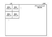
- FIG. 5 is a plan view of an example of the address event detection unit 260 applicable to each embodiment.
- a plurality of detection blocks 32 are arranged in the address event detection unit 260.
- the detection block 32 is arranged for each shared block 221 on the light receiving chip 201.
- N is an integer
- N detection blocks 32 are arranged.
- Each detection block 32 is connected to the corresponding shared block 221.
- FIG. 6 is a diagram showing a configuration of an example of a light receiving circuit 31 and a detection block 32 applicable to each embodiment.
- the output of the light receiving circuit 31 is supplied to the detection block 32.
- the detection block 32 includes a buffer 33 and a detection circuit 34.
- the light receiving circuit 31 includes a photoelectric conversion element 310, transistors 311a, 311b, 312a and 312b which are nMOS (n-channel MetalOxide Semiconductor) transistors, and a transistor 313 which is a pMOS (p-channel MOS) transistor. , Equipped with.
- the photoelectric conversion element 310 and the transistors 311a, 311b, 312a and 312b are arranged on the light receiving chip 201, for example, and the transistor 313 is arranged on the detection chip 202.
- the photoelectric conversion element 310 outputs the photocurrent I pht according to the light reception.
- the source of the transistor 311b is connected to the cathode of the photoelectric conversion element 310, and the drain is connected to the source of the transistor 311a.
- the drain of the transistor 311a is connected to the power supply terminal Vdd.
- the anode of the photoelectric conversion element 311 is connected to the ground terminal.
- the gate of the transistor 312b is connected to the connection point between the cathode of the photoelectric conversion element 310 and the drain of the transistor 311b.
- the source of the transistor 312b is connected to the ground terminal and the drain is connected to the source of the transistor 312a.
- the gate of the transistor 311b is connected to the connection point between the drain of the transistor 312b and the source of the transistor 312a.
- the drain of the transistor 312a is connected to the source of the transistor 313.
- the drain of the transistor 313 is connected to the power supply terminal Vdd, and a predetermined bias voltage V bias is applied to the gate.
- the gate of the transistor 311a is connected to the connection point between the drain of the transistor 312a and the source of the transistor 313.
- the drains of the transistors 311b and 312b are connected to the power supply side, respectively, and form a source follower circuit, respectively.
- the two source follower circuits with the transistors 311b and 312b are connected in a loop.
- the drain is connected to the power supply side to form a source follower circuit, and the two source follower circuits by these transistors 311a and 312a are connected in a loop. That is, the light receiving circuit 31 shown in FIG. 6 includes a configuration in which a circuit in which two source follower circuits are connected in a loop is connected in series.
- the photocurrent I pht output from the photoelectric conversion element 310 is converted into a voltage signal corresponding to the logarithmic value by the configuration in which the circuits in which the two source follower circuits are connected in a loop are connected in series. Further, the transistor 313 supplies a constant current to the transistors 312a and 312b. In this way, the light receiving circuit 31 functions as a generation unit that generates a voltage corresponding to the logarithmic value of the photocurrent.
- the ground of the light receiving chip 201 and the ground of the detection chip 202 are separated from each other as a countermeasure against interference.
- the voltage signal in which the optical current I pht is converted according to its logarithmic value is taken out from the connection point between the source of the transistor 313 and the drain of the transistor 312a, and the transistors 331 and 332, which are nMOS transistors, are taken out, respectively. It is input to the detection circuit 34 as a voltage signal V pd via the included buffer 33.
- the detection circuit 34 includes a detection unit 340a, a memory 341, and a transfer circuit 342.
- the detection unit 340a is supplied with the reset signal RST and the threshold voltage Vb, for example, from the row drive circuit 251.
- the detection unit 340a performs determination processing based on the threshold value Vth for the voltage signal V pd input from the light receiving circuit 31 via the buffer 33, and outputs a signal V comp indicating a change in the light receiving amount in the photoelectric conversion element 310. ..
- the signal V comp includes a signal V ON indicating a change in the received light amount in the positive (+) direction and a signal V OFF indicating a change in the negative (-) direction, and indicates the occurrence of an address event.
- FIG. 7 is a diagram showing an example of the configuration of the detection unit 340a by the existing technology.
- the detection unit 340a by the existing technique Fig. The configuration shown in 1 is applied.
- the detection unit 340aa includes a capacitor C 1 , a comparator 3400, and a reset circuit 3401.
- a voltage signal V pd is supplied to the first electrode, and an electric charge generated in response to light reception is supplied to the capacitor C 1 by the photoelectric conversion element 310.
- the second electrode of the capacitor C 1 is connected to the inverting input end ( ⁇ ) of the comparator 3400.
- the signal input to the inverting input end (-) of the comparator 3400 is a signal V diff that changes according to a change in the voltage signal V pd input to the first electrode of the capacitor C 1 .
- the threshold voltage Vb supplied from the row drive circuit 251 is input to the non-inverting input end (+) of the comparator 3400.
- the signal V comp output from the comparator 3400 is supplied to the memory 341 and stored.
- the memory 341 is configured by a sampling circuit.
- the sampling circuit can be realized by using, for example, a switch and a capacitor.
- the memory 341 may be configured by a memory circuit such as a latch circuit or a flip-flop circuit.
- the reset circuit 3401 is connected to the connection point between the second electrode of the capacitor C 1 and the inverting input end ( ⁇ ) of the comparator 3400.
- the reset circuit 3401 is supplied with the reset signal RST from the row drive circuit 251.
- the reset signal RST is a signal for selecting the time for activating the reset circuit 3401.
- the row drive circuit 251 outputs a reset signal RST according to the signal V comp stored in the memory 341.
- the reset circuit 3401 is activated by the reset signal RST to reset the state of the second electrode of the capacitor C 1. Therefore, at the second electrode of the capacitor C 1 , the signal V diff of the difference between the current voltage signal V pd and the past voltage signal V pd appears.
- the comparator 3400 compares the voltage of this signal V diff with the threshold voltage Vb, and outputs the signal V comp as the comparison result.
- the transfer circuit 342 for example, according to the column drive signal supplied from the column driver circuit 252 under the control of the control unit 130 reads the signal V comp from the memory 341, the read signal V comp, It is output from the detection block 32 as a detection output indicating the detection result of the address event by the detection block 32.
- This detection output is supplied to, for example, the signal processing circuit 240.
- the signal processing circuit 240 performs predetermined signal processing such as image recognition processing based on the detection output supplied from the detection block 32.
- the detection output subjected to predetermined signal processing by the signal processing circuit 240 is recorded in, for example, the recording unit 120. Not limited to this, the detection output from the detection block 32 may be directly recorded on the recording unit 120.
- the operation of the comparator 3400 by the existing technology will be explained in more detail.
- the comparator 3400 detects an event in which the amount of light received by the photoelectric conversion element 310 increases and an event in which the amount of light received decreases.
- the event in which the amount of light increases is referred to as a (+) event
- the event in which the amount of light decreases is referred to as a (-) event.
- the row drive circuit 251 When the event is detected, the row drive circuit 251 outputs the threshold voltage Vb of the voltage V off and supplies it to the comparator 3400, for example, according to the control of the control unit 130. On the other hand, when the (+) event is detected, the row drive circuit 251 outputs a threshold voltage Vb having a voltage V on lower than the voltage V off and supplies it to the comparator 3400, for example, according to the control of the control unit 130.
- the row drive circuit 251 repeats, for example, voltage V off , voltage V on, and voltage V reset in chronological order to output as a threshold voltage Vb.
- the voltage V reset is, for example, a voltage value between the voltage V off and the voltage V on.
- the comparator 3400 When detecting an event, the comparator 3400 sets the signal V comp to a high level when the voltage of the signal V diff is less than the threshold voltage Vb which is the voltage V off , and this signal V comp is the memory 341. Is remembered in. This indicates that a (-) event, that is, a decrease in the amount of light, has been detected. If the voltage of the signal V diff is equal to or higher than the threshold voltage Vb (voltage V off ), the signal V comp output from the comparator 3400 becomes a low level, indicating that a decrease in the amount of light is not detected. ..
- the comparator 3400 sets the signal V comp to the low level when the voltage of the signal V diff exceeds the threshold voltage Vb which is the voltage V on , and this signal V comp is stored in the memory 341. It will be remembered. This indicates that a (+) event, that is, an increase in the amount of light, has been detected. If the voltage of the signal V diff is equal to or less than the threshold voltage Vb (voltage V on ), the signal V comp output from the comparator 3400 becomes a high level, indicating that an increase in the amount of light is not detected.
- the control unit 130 acquires the contents of the memory 341 via the row drive circuit 251, and based on the acquired contents of the memory 341 and the threshold voltage Vb, the signal from the memory 341 to the column drive circuit 252. Instructs to read V comp.
- the operation of the light receiving circuit 31 and the detection block 32 according to the existing technique will be described more specifically.
- the change in the amount of light received by the photoelectric conversion element 310 is converted into a change in the voltage signal V pd by the logarithmic conversion circuit included in the light receiving circuit 31.
- the reset circuit 3401 is not active and does not conduct, the change in the voltage signal V pd is reflected in the signal V diff input to the inverting input end (-) of the comparator 3400 via the capacitor C 1. This is because the voltage across the capacitor C 1 stays at a constant voltage.
- the comparator 3400 When the comparator 3400 is selected by the row drive circuit 251 , the voltage of the signal V diff input to the inverting input terminal ( ⁇ ) and the non-inverting input terminal (+) at the second electrode of the capacitor C 1 Compare with the applied threshold voltage Vb. The comparator 3400 outputs the signal V comp as a comparison result.
- the signal V comp output from the comparator 3400 is stored in the memory 341 by, for example, the row drive circuit 251.
- the row drive circuit 251 determines that the signal V comp stored in the memory 341 indicates a change in the amount of light received by the photoelectric conversion element 310 based on the stored contents of the memory 341 and the threshold voltage Vb , and resets the signal V comp.
- the reset circuit 3401 is conducted.
- the reset circuit 3401 becomes conductive, the voltage of the signal V diff at the inverting input end ( ⁇ ) of the comparator 3400 is reset to a known level. Therefore, the current voltage signal V pd is stored in the capacitor C 1.
- the contrast sensitivity can be lowered by controlling the threshold voltage Vb applied to the comparator 3400.
- the control range of the contrast sensitivity is limited to the settable voltage range of the threshold voltage Vb.
- the comparator in the DVS circuit is connected in two stages, and the gain of the comparator on the input side is set lower than the gain of the comparator on the output side.
- the range of the voltage signal V pd that can be input to the comparator on the input side can be expanded, and the contrast of the DVS circuit can be reduced.
- FIG. 8A is a diagram showing an example of the configuration of the detection unit 340b according to the first embodiment.
- the detection unit 340b includes a capacitor C 1 , comparators 40a and 41a connected in series, respectively having a configuration as an amplifier, and switch circuits 42 and 43.
- the voltage signal V pd output from the light receiving circuit 31 is applied to the first electrode of the capacitor C 1 via the buffer 33, and the signal V diff from the second electrode is the first amplifier on the input side. It is input to the inverting input terminal (-) which is the first input end of the comparator 40a as an amplifier.
- the selective output end of the switch circuit 42 is connected to the non-inverting input end (+), which is the second input end of the comparator 40a.
- the switch circuit 42 includes three selective input ends 42a, 42b and 42c. Voltages V az , Vb on and Vb off are applied to the selective input terminals 42a, 42b and 42c, respectively.
- the voltage Vb on is a threshold value for determining the (+) event.
- the voltage Vb off is a threshold value for determining the ( ⁇ ) event.
- the voltage V az is, for example, a voltage between the voltage Vb on and the voltage Vb off, and is a voltage at a reset level for resetting the event detected immediately before.
- one of the input ends 42a, 42b and 42c is selected according to a control signal (not shown) from the row drive circuit 251 and the voltage applied to the selected input ends is applied to the selected input ends 42a, 42b and 42c.
- the threshold voltage Vb A0 which is the first reference voltage signal, is applied to the non-inverting input end (+) of the comparator 40a.
- the voltage of the signal V diff applied to the inverting input end ( ⁇ ) of the comparator 40a is directed from the voltage V az to the voltage V b on.
- a (+) event is detected.
- voltage of the signal V diff is, toward the voltage V az in the direction of the voltage Vb off, if it exceeds a voltage Vb off, (-) The event is detected.
- the voltage of the signal V diff is, toward the voltage V az in the direction of the voltage Vb on, does not exceed a voltage Vb on, and, toward the voltage V az in the direction of the voltage Vb off, does not exceed the voltage Vb off In this case, neither the (+) event nor the (-) event is detected.
- the voltage of the signal V diff is, toward the voltage V az in the direction of the voltage Vb on, exceeds the voltage Vb on
- the voltage of the “signal V diff is the voltage Vb on
- the voltage of the signal V diff exceeds the voltage Vb off from the voltage V az toward the voltage Vb off
- the voltage of the signal V diff exceeds the voltage Vb off. It will be explained as “ta”.
- the voltage of the signal V diff exceeds the voltage Vb on " and “the voltage of the signal V diff exceeds the voltage Vb off” are summarized as "the voltage of the signal V diff exceeds the threshold voltage Vb A0" . It may be said that it has exceeded.
- these voltages Vb on and Vb off have variable voltage values.
- the larger the absolute value of the difference between the voltage values of the voltages Vb on and Vb off and the voltage V az the lower the detection sensitivity (contrast sensitivity) of the change in the amount of light. This corresponds to lowering the gain of the comparator 40a.
- the voltages Vb on and Vb off function as a gain changing unit that changes the gain of the comparator 40a.
- the output from which any of the voltages Vb on , Vb off, and V az is selected is applied to the inverting input end ( ⁇ ) of the comparator 40a as the threshold voltage Vb A00.
- the comparator 40a compares the threshold voltage Vb A0 applied to the non-inverting input end (+) with the voltage of the signal V diff input to the inverting input terminal (-), and outputs the signal V comp1 as a comparison result. ..
- the output end of the comparator 40a is connected to the inverting input terminal (-) as the third input terminal of the comparator 41a as the second amplifier which is the output side amplifier, and is also connected to one end of the switch circuit 43. ..
- the other end of the switch circuit 43 is connected to the connection point between the second electrode of the capacitor C 1 and the inverting input end ( ⁇ ) of the comparator 40a.
- the switch circuit 43 corresponds to the reset circuit 3401 shown in FIG. 7, and the conduction / non-conduction state is controlled by, for example, a control signal (not shown) from the row drive circuit 251.
- a control signal not shown
- a predetermined threshold voltage Vb A1 as a second reference voltage is applied to the non-inverting input terminal (+) as the fourth input terminal.
- the comparator 41a compares the signal V comp1 applied to the inverting input end ( ⁇ ) with the threshold voltage Vb A1 input to the non-inverting input end (+), and outputs a signal V comp2 indicating the comparison result.
- This signal V comp2 is output from the detection unit 340a and stored in the memory 341.
- FIG. 8B is a circuit diagram showing an example of the configuration of the detection unit 340b according to the first embodiment.
- the comparator 40a includes a transistor 401 which is a pMOS transistor and a transistor 402 which is an nMOS transistor. Further, in this example, the switch circuit 43 is composed of an nMOS transistor.
- the source is connected to the power supply terminal Vdd and the drain is connected to the drain of the transistor 402.
- the source of the transistor 402 is connected to the ground terminal.
- the signal V comp1 which is the output of the comparator 40a is taken out from the connection point between the drain of the transistor 401 and the drain of the transistor 402.
- one end of the switch circuit 43 (for example, a drain of an nMOS transistor) is connected to the connection point.
- the second electrode of the capacitor C 1 is connected to the gate of the transistor 401, and the other end of the switch circuit 43 (for example, the source of the nMOS transistor) is connected to the connection point between the gate of the transistor 401 and the capacitor C 1.
- the comparator 41a includes a transistor 411 which is a pMOS transistor and a transistor 412 which is an nMOS transistor.
- the source of the transistor 411 is connected to the power supply terminal Vdd and the drain is connected to the drain of the transistor 412.
- the source of transistor 412 is connected to the ground terminal.
- connection point between the drain of the transistor 401 in the comparator 40a and the drain of the transistor 402 is connected to the gate of the transistor 411 in the comparator 41a. That is, the signal V comp1 which is the output of the comparator 40a taken out from the connection point is applied to the gate of the transistor 411. A predetermined threshold voltage Vb A1 is applied to the gate of the transistor 412. The signal V comp2, which is the output of the comparator 41a, is taken out from the connection point between the drain of the transistor 411 and the drain of the transistor 412.
- the comparator 40a compares the voltage of the signal V diff applied to the gate of the transistor 401 with the threshold voltage Vb A0 applied to the gate of the transistor 402. As a result of comparison, when the voltage of the signal V diff exceeds the threshold voltage Vb A0 , the comparator 40a changes the state of the signal V comp1 which is the output of the comparator 40a from, for example, a high level to a low level.
- the comparison operation by the comparator 40a will be described.
- the threshold voltage Vb A0 voltage Vb on , Vb off, or V az
- the drain of the transistor 402 corresponds to the voltage applied to the gate.
- the drain current Ids n flows.
- a drain current Ids p flows through the transistor 401 when a voltage (voltage V diff ) at the gate of the transistor 401, which is a pMOS transistor, is applied.
- the comparator 41a compares the signal V comp1 which is the output of the comparator 40a with the threshold voltage Vb A1 applied to the gate of the transistor 412. When the signal V comp1 exceeds the threshold voltage Vb A1 , the comparator 41a changes the state of the signal V comp2, which is the output of the comparator 41a, from, for example, a low level to a high level.
- the drain current Ids n of the transistor 402 changes depending on the gate potential of the transistor 402, which is an nMOS transistor.
- the drain current Ids p in the transistor 401 which is a pMOS transistor, which is balanced with the drain current Ids n , also changes.
- the potential applied to the gate of the transistor 401 also changes, and the threshold value appears to change from the transistor 401.
- changes in the threshold voltages Vb on and Vb off in the direction in which the amount of change in the gate potential of the transistor 401 required up to the threshold becomes large appear to have reduced the inversion ability of the comparator 40a, and the comparator 40a It can be considered equivalent to lowering the gain.
- the comparator 40a has an inverting input terminal (-) with respect to the signal V diff input to the threshold determination by the threshold voltage Vb a0, configured to run slowly compared to a threshold decision in the comparator 41a. That is, in the comparator 40a, the falling (or rising) speed of the signal V comp1 when the voltage (signal V diff ) input to the inverting input end (-) exceeds the threshold voltage Vb A0 is inverted in the comparator 41a.
- the voltage (signal V comp1 ) input to the input end (-) is set to be slower than the rising (or falling) speed of the signal V comp2 when the threshold voltage Vb A1 is exceeded.
- the transistors 401 and 411 are used as pMOS transistors, and the transistors 402 and 412 are used as nMOS transistors, respectively, but this is not limited to this example.
- the transistors 401 and 411 may be nMOS transistors, respectively, and the transistors 402 and 412 may be pMOS transistors, respectively.
- FIG. 9 is a schematic diagram for explaining the operation of the detection unit 340b according to the first embodiment.
- the horizontal axis represents time and the vertical axis represents each voltage.
- Section (a) of FIG. 9 shows an example of the operation of the detection unit 340a by the existing technique described with reference to FIG. 7.
- the upper part of this section (a) shows the voltage signal V pd applied to the first electrode of the capacitor C 1
- the lower part shows the signal V comp output from the comparator 3400. Further, here, the (+) event in which the amount of light is increased is shown.
- the voltage signal V pd is assumed that for example, starts increasing at time t 10.
- Comparator 3400 at time t 10 is outputting a signal V comp high state.
- the comparator 3400 outputs a high voltage V comp. It is assumed that the voltage signal V pd exceeds the threshold voltage Vb at time t 12.
- the comparator 3400 the fall begins in front of the time t 11 from the signal V comp time t 11, at time t 13, and the fall of the signal V comp is completed, the signal V comp is a transition to a low state.
- Section (b) of FIG. 9 shows an example of the operation of the detection unit 340b according to the first embodiment described with reference to FIGS. 8A and 8B. Similar to the above, the upper part of this section (b) shows the voltage signal V pd applied to the first electrode of the capacitor C 1 , the middle part shows the signal V comp1 output from the comparator 40a, and the lower part further shows. Indicates the signal V comp2 output from the comparator 41a.
- the change in the voltage signal V pd in the upper part of the section (b) is the same as the change in the voltage signal V pd in the upper part of the section (a). Further, it is assumed that the threshold voltage Vb A0 in the comparator 40a is the same as the threshold voltage Vb in the comparator 3400.
- the voltage signal V pd starts to rise at time t 20 (corresponding to the above time t 10 ), for example.
- the comparator 40a outputs a high signal V comp1. It is assumed that the voltage signal V pd exceeds the threshold voltage Vb A0 at time t 21.
- the slope of the rise of the voltage signal V pd is the same as the slope in the section (a) of FIG. 9, and the time t 20 to t 21 is the same as the time t 10 to t 11 described above. It shall be.
- the falling edge of signal V comp1 is started from the front of the time t 21 the time t 21.
- the falling start time t 21 is a time before the above time t 11. Will be.
- the comparator 41a compares this signal V comp1 with the threshold voltage Vb A1 .
- the comparator 41a outputs the low signal V comp2. It is assumed that the voltage of the signal V comp1 exceeds the threshold voltage Vb A1 at time t 24. In this case, the voltage of the signal V comp1 exceeds the threshold voltage Vb A1 in the negative direction.
- the comparator 41a it is started rising in front of the time t 23 signal V comp2 from time t 24, at time t 25, and the rise of the signal V comp2 is completed, the signal V comp2 is transited to high state.
- This time t 25 corresponds to the determination result by the threshold voltage Vb A1 for the slowly changing signal V comp1. Therefore, according to the existing technology, the time is delayed more than the time t 13 when the determination by the threshold voltage Vb is directly performed for the voltage signal V pd. Therefore, according to the detection unit 340b according to the first embodiment, by appropriately setting the threshold voltage Vb A1 for the comparator 41a, the input change amount ⁇ V pd until the determination of the voltage signal V pd is input by the existing technique. It is possible to take a larger amount than the change amount ⁇ V pd. As a result, the contrast sensitivity can be lowered as compared with the detection unit 340a according to the existing technology.
- the slow change of the signal V comp1 can generally be realized by changing the circuit constant.
- the change in the signal V comp1 can be moderated by reducing the gain of the comparator 40a by increasing the drain current of the transistor 402 or reducing the W size of the transistor 401.
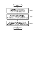
- FIG. 10 is a flowchart of an example for explaining the operation of the detection unit 340b according to the first embodiment.
- step S100 in the detection unit 340b, the voltage of the voltage signal V pd corresponding to the logarithmic value of the photocurrent I pht output from the photoelectric conversion element 310 is applied to the first electrode of the capacitor C 1.
- the comparator 40a as the first amplifier having the first gain is applied to the first input end which is the inverting input end ( ⁇ ), and the first capacitor C 1 is applied.
- the voltage of the signal V diff of the 2 electrodes is compared with the reference voltage of 1 applied to the second input end which is the non-inverting input end (+).
- the first reference voltage is the threshold voltage Vb A0 at which the voltages Vaz , Vb on and Vb off are switched at predetermined timings.
- the comparator 40a outputs the signal V comp1 as a comparison result of comparing the voltage of the signal V diff and the threshold voltage Vb A0.
- the signal V comp1 output from the comparator 40a is input to the third input end (-) of the comparator 41a as a second amplifier having a second gain higher than the first gain. ..
- the comparator 41a has the voltage of the signal V comp1 which is the output of the comparator 40a input to the third input end and the fourth as the non-inverting input end (+). Compare with the second reference voltage applied to the input end.
- the second reference voltage is a predetermined threshold voltage Vb A1 .
- the comparator 41a compares the voltage of the signal V comp1 output from the comparator 40a with the threshold voltage Vb A1, and outputs the signal V comp2 as a comparison result.
- the signal V comp2 output from the comparator 41a is output from the detection unit 340b and stored in the memory 341, for example.
- FIG. 11A is a diagram showing an example of the configuration of the detection unit 340c according to the first modification of the first embodiment.
- the voltages Vb on and Vb off applied to the selective input terminals 42b and 42c of the switch circuit 42 have fixed voltage values, respectively. Further, the gain of the comparator 40b is variable.
- FIG. 11B is a circuit diagram showing an example of the configuration of the detection unit 340c according to the first modification of the first embodiment.
- transistors 403 and 404 which are pMOS transistors, are added to the comparator 40a shown in FIG. 8B described above, respectively.
- Other configurations are the same as the configurations described with reference to FIG. 8B, and thus the description thereof will be omitted here.
- the gate is connected to the gate of the transistor 401, the source is connected to the source of the transistor 401, and the drain is connected to the source of the transistor 404. Further, in the transistor 404, the drain is connected to the drain of the transistor 401. That is, the transistor 403 is connected in parallel with the transistor 401 when the transistor 404 is in the ON state. Therefore, by controlling the voltage applied to the gate of the transistor 404, it is possible to switch whether the transistor 401 is used alone or connected in parallel with the transistor 403. That is, by controlling the voltage applied to the gate of the transistor 404, the elements constituting the comparator 40b can be switched.
- the transistors 401 and 403 By connecting the transistors 401 and 403 in parallel, it is possible to obtain a larger gain than when the transistors 401 are used alone. For example, in normal or weak light intensity environment, the transistor 404 is turned on and the transistors 401 and 403 are connected in parallel, and in the high light intensity environment, the transistor 404 is turned off and the transistor 401 is used alone. Can be considered.
- the gain of the comparator 40b on the input side can be changed, so that the contrast sensitivity is lowered as compared with the detection unit 340a by the existing technology. Can be made to.
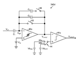
- FIG. 12 is a diagram showing an example of the configuration of the detection unit 340d according to the second modification of the first embodiment.
- the comparator 40c is configured by, for example, a circuit similar to the comparator 40a shown in FIG. 8B, and is subjected to negative feedback by the capacitor C 2 and the capacitor C 3 via the switch circuit 46 to obtain an amplifier (operational amplifier). ) Can be used.
- the output end of the comparator 40c is connected to one end of the switch circuit 43, one end of the capacitor C 2 , and one end of the switch circuit 46.
- the other end of the switch circuit 46 is connected to one end of the capacitor C 3.
- the other ends of the switch circuit 43 and the capacitors C 2 and C 3 are connected to the inverting input end ( ⁇ ) of the comparator 40c. Further, a voltage V az is applied to the non-inverting input end (+) of the comparator 40c.
- the output end of the comparator 40c is connected to the inverting input end ( ⁇ ).
- the selected output end of the switch circuit 44 is connected to the non-inverting input end (+) of the comparator 41a.
- Voltages Vb on and Vb off are connected to the selective input ends 44a and 44b of the switch circuit 44, respectively.
- the switch circuit 44 selects one of the selection input ends 44a and 44b according to the control of the row drive circuit 251 and sets one of the voltages Vb on and Vb off as the threshold voltage Vb A1 as the non-inverting input end of the comparator 41a. Enter in (+).
- the gain G of the comparator 40c as an amplifier is determined based on the ratio of the capacitance of the capacitor C 1 to the capacitance of the capacitor to be negatively feedback connected. That is, the gain G of the comparator 40c is obtained by the following equation (1) when the switch circuit 46 is in the conductive state and by the following equation (2) when the switch circuit 46 is in the non-conducting state.
- G C 1 / (C 2 + C 3 )... (1)
- G C 1 / C 2 ... (2)
- the switch circuit 46 functions as a gain changing unit that changes the capacitance of the capacitors C2 and C3 as the elements constituting the comparator 40c and changes the gain of the comparator 40c.
- the switch circuit 46 when the switch circuit 46 is used in an environment with a large amount of light, a large change in the amount of light can be detected by setting the switch circuit 46 in a conductive state, and in an environment where the amount of light is weak, the switch circuit 46 is set in a non-conducting state to detect a weak change in the amount of light. It can be possible.
- the signal V comp1 output from the comparator 40a is input to the inverting input end ( ⁇ ) of the comparator 41a.
- the comparator 41a combines the threshold voltage Vb A1 due to the voltage Vb on or Vb off applied to the non-inverting input terminal (+) via the switch circuit 44 and the signal V comp1 input to the inverting input terminal (-). The comparison is performed, and the signal V comp2 is output as the comparison result.
- FIG. 13 is a diagram showing an example of the configuration of the detection unit 340e according to the third modification of the first embodiment.
- the comparator 40c is configured by, for example, the same circuit as the comparator 40a shown in FIG. 8B, and is subjected to negative feedback by a capacitor C 2 connected in parallel and a resistor R 2 which is a variable resistor to obtain an amplifier ( It can be used as an operational amplifier).
- the output end of the comparator 40c is connected to one end of the switch circuit 43, one end of the capacitor C 2 , and one end of the resistor R 2.
- the other ends of each of the capacitor C 2 and the resistor R 2 are connected to the inverting input end ( ⁇ ) of the comparator 40c.
- the other end of the resistor R 1 having a variable resistance value to which the voltage signal V pd is input to one end is connected to the first electrode of the capacitor C 1.
- the second electrode of the capacitor C 1 is connected to the inverting input end ( ⁇ ) of the comparator 40c together with the other ends of the capacitor C 2 and the resistor R 2.
- comparator 41a Since the comparator 41a has the same configuration as shown in FIG. 12, the description thereof is omitted here.
- the gain G of the comparator 40c as an amplifier is determined based on the ratio of the resistance value of the resistor R1 to the resistance value of the resistor R2 connected by negative feedback. That is, the gain G of the comparator 40c is obtained by the following equation (3).
- G R 2 / R 1 ... (3)
- the gain G of the comparator 40c can be changed by changing the resistance value of at least one of the resistors R 1 and R 2.
- the gain G of the comparator 40c can be made smaller, and the signal V diff at the inverting input end (-) can be made smaller. It is possible to widen the dynamic range for. That is, at least one of the resistors R 1 and R 2 functions as a gain changing unit that changes the resistance of the resistors R 1 or R 2 as an element constituting the comparator 40c and changes the gain of the comparator 40c.
- the resistance value of the resistor R 2 when used in an environment with a large amount of light, the resistance value of the resistor R 2 can be reduced to detect a large change in the amount of light, and the resistance value of the resistor R 2 can be increased in an environment where the amount of light is weak. It is possible to detect a weak change in the amount of light.
- the signal V comp1 output from the comparator 40a is input to the inverting input end ( ⁇ ) of the comparator 41a.
- the comparator 41a combines the threshold voltage Vb A1 due to the voltage Vb on or Vb off applied to the non-inverting input terminal (+) via the switch circuit 44 and the signal V comp1 input to the inverting input terminal (-). The comparison is performed, and the signal V comp2 is output as the comparison result.
- FIG. 14A is a diagram showing an example of the configuration of the detection unit 340f according to the second embodiment.
- the detector 340f includes a capacitor C 1 , comparators 40a and 41a connected in series, respectively having a configuration as an amplifier, and switch circuits 43 and 44.
- the voltage signal V pd output from the light receiving circuit 31 is applied to the first electrode of the capacitor C 1 via the buffer 33, and the signal V diff from the second electrode is the input side amplifier of the comparator 40a. It is input to the inverting input end (-). A voltage V az is applied to the non-inverting input end (+) of the comparator 40a.
- the comparator 40a has an inverting input terminal (-) with respect to the signal V diff input to the threshold determination by the threshold voltage Vb a0, comparator It is configured to be executed more slowly than the threshold value determination in 41a.
- the signal V comp1 output from the comparator 40a is input to the inverting input end ( ⁇ ) of the comparator 41a.
- the selective output end of the switch circuit 45 is connected to the non-inverting input end (+) of the comparator 41a.
- voltages Vb on and Vb off whose voltage values are variable are connected to the selection input terminals 45a and 45b, respectively.
- the switch circuit 45 selects one of the selection input ends 45a and 45b according to the control of the row drive circuit 251 and sets one of the voltages Vb on and Vb off as the threshold voltage Vb A1 as the non-inverting input end of the comparator 41a. Enter in (+).
- these voltages Vb on and Vb off have variable voltage values.
- the smaller the absolute value of the difference between the voltage values of the voltages Vb on and Vb off and the voltage V az the higher the detection sensitivity (contrast sensitivity) of the change in the amount of light.
- the gain of the comparator 40a becomes relatively low.
- the voltages Vb on and Vb off function as a gain changing unit that changes the gain of the comparator 41a.
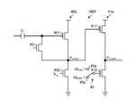
- FIG. 14B is a circuit diagram showing an example of the configuration of the detection unit 340f according to the second embodiment.
- the comparator 40a shown in FIG. 14B has the same configuration as the comparator 40a shown in FIG. 8B except that a voltage Vaz is applied to the gate of the transistor 402.
- the comparator 41a has the same configuration as the comparator 41a shown in FIG. 8B except that a voltage Vb on or a voltage Vb off is applied to the gate of the transistor 412 via the switch circuit 45.
- the gain of the comparator 40a can be relatively gained by making the voltages Vb on and Vb off applied as the threshold voltage Vb A1 to the comparator 41a on the output side variable. It is possible to reduce the contrast sensitivity. For example, when the voltages Vb on and Vb off applied to the comparator 41a on the output side are used in an environment where the absolute value of the difference between the voltages Vb on and Vb off and the voltage V az is normal or a weak light amount, they are normal values, respectively. However, it is conceivable to change to a lower value when used in an environment with a large amount of light.
- the signal V comp1 input to the comparator 41a on the output side has already been amplified by the comparator 40a on the input side. It is disadvantageous for the morphology and each variation thereof. On the other hand, when a plurality of input-side configurations, which will be described later, are shared by one output-side configuration, it is possible to reduce the number of threshold control lines for controlling the switch circuit 45.
- FIG. 15A is a diagram showing an example of the configuration of the detection unit 340 g according to the modified example of the second embodiment.
- the voltages Vb on and Vb off applied to the selective input terminals 45a and 45b of the switch circuit 45 are fixed voltage values, respectively. Further, the gain of the comparator 41b is variable.
- the comparator 40b determines the threshold value by the voltage V az for the signal V diff input to the inverting input end ( ⁇ ). , It is configured to be executed more slowly than the threshold value determination in the comparator 41b.
- FIG. 15B is a circuit diagram showing an example of the configuration of the detection unit 340 g according to the modified example of the second embodiment.
- transistors 413 and 414 which are pMOS transistors
- transistors 415 and 416 which are nMOS transistors, respectively, are added to the comparator 41a shown in FIG. 14B described above.
- Other configurations are the same as the configurations described with reference to FIG. 14B, and thus the description thereof will be omitted here.
- the gate is connected to the gate of the transistor 411
- the source is connected to the source of the transistor 411
- the drain is connected to the source of the transistor 414.
- the drain is connected to the drain of the transistor 411. That is, the transistor 413 is connected in parallel with the transistor 411 when the transistor 414 is in the ON state. Therefore, by controlling the voltage applied to the gate of the transistor 414, it is possible to switch whether the transistor 411 is used alone or connected in parallel with the transistor 413.
- the gate is connected to the gate of the transistor 412
- the source is connected to the source of the transistor 412
- the drain is connected to the source of the transistor 415.
- the drain is connected to the drain of the transistor 412. That is, the transistor 416 is connected in parallel with the transistor 412 when the transistor 415 is in the ON state. Therefore, by controlling the voltage applied to the gate of the transistor 415, it is possible to switch whether the transistor 412 is used alone or connected in parallel with the transistor 416.
- the elements constituting the comparator 41b can be switched.
- the transistors 414 and 415 are controlled so as to be in the on state or the off state at the same time.
- the transistors 411 and 413 and the transistors 412 and 416 are connected in parallel, respectively, it is possible to obtain a larger gain as compared with the case where the transistors 411 and 412 are used alone.
- the transistors 411 and 413 are connected in parallel with the transistors 414 and 415 turned on, respectively, and the transistors 412 and 416 are connected in parallel, respectively. It is conceivable to use the transistors 411 and 412 independently with the and 416 turned off, respectively.
- the gain of the comparator 41b on the output side can be changed, so that the contrast sensitivity can be lowered as compared with the detection unit 340a by the existing technology. can.
- the third embodiment is an example in which the output side comparator is shared by the input side comparators in the plurality of detection blocks 32 among the two comparators connected in series.
- FIG. 16 is a diagram showing an example of the configuration of the detection unit 340h according to the third embodiment.
- two comparators 40a 1 and 40a 2 on the input side are shared by one comparator 41a on the output side. This is not limited to this example, and it is also possible to share three or more comparators 40a on the input side with one comparator 41a on the output side.
- one shared block 221 includes two light receiving circuits 31, and these two light receiving circuits 31 correspond to two detection blocks 32, respectively (see FIG. 5).
- a buffer 33 and an input side comparator 40a included in the detection unit 340 are provided corresponding to each of the two light receiving circuits 31.
- the output-side comparator 41a included in the detection unit 340, and the memory 341 and transfer circuit 342 included in the detection circuit 34 are shared by the two light receiving circuits 31.
- the comparators 40a 1 and 40a 2 can be applied with the same circuit as the comparator 40a described with reference to, for example, FIG. 8B, respectively.
- the selective output of one switch circuit 42 is commonly connected to the non-inverting input ends (+) of the comparators 40a 1 and 40a 2.
- Voltages Vaz , Vb on and Vb off are applied to the selective input ends 42a, 42b and 42c of the switch circuit 42, respectively. Of these, the voltages Vb on and Vb off are variable.
- the output of the switch circuit 42 is commonly applied to the comparators 40a 1-1 and 40a 1-2 as the threshold voltage Vb A0.
- the voltage signal V pd1 output from one of the two light receiving circuits 31 shared by the comparator 41a is applied to the first electrode of the capacitor C 1-1.
- the second electrode of the capacitor C 1-1 is connected to the inverting input end ( ⁇ ) of the comparator 40a 1.
- the output of the comparator 40a 1 is connected to one end of the switch circuit 47 1.
- the output of the comparator 40a 1 through the switch circuit 43 1, a capacitor C 1-1 and the inverting input terminal of the comparator 40a 1 - is connected to the connection point between the ().
- the voltage signal V pd2 output from the other of the two light receiving circuits 31 shared by the above-mentioned comparator 41a is applied to the first electrode of the capacitor C 1-2.
- the second electrode of the capacitor C 1-2 is connected to the inverting input end ( ⁇ ) of the comparator 40a 2.
- the output of the comparator 40a 2 is connected to one end of the switch circuit 47 2.
- the output of the comparator 40a 2 through the switch circuit 43 2, the inverting input terminal of the capacitor C 1-2 and comparator 40a 2 - is connected to the connection point between the ().
- the comparator 40a 1 and 40a 2 are inverting input terminal (-) with respect to the signal V diff1 and V diff2 input to the threshold voltage Vb
- the threshold value determination by A0 is configured to be executed more slowly than the threshold value determination by the comparator 41a.
- the other ends of the switch circuits 47 1 and 47 2 are connected to the inverting input end (-) of the comparator 41a.
- the threshold voltage Vb A1 is applied to the non-inverting input end (+) of the comparator 41a.
- Switch circuits 47 1 and 47 2 are conductive state and nonconductive state is exclusively controlled.
- the signal V COMP1-1 output from the comparator 40a 1 through the switch circuit 47 1 inverting input terminal of the comparator 41a - is input to the ().
- the comparator 41a compares the signal V comp1-1 input to the inverting input end (-) with the threshold voltage Vb A1 input to the non-inverting input end (+), and obtains the signal V comp2-1 as a comparison result. Output to memory 341.
- signal V COMP1-2 output from the comparator 40a 2 through the switch circuit 47 2-inverting input terminal of the comparator 41a - is input to the ().
- the comparator 41a compares the signal V comp1-2 input to the inverting input end (-) with the threshold voltage Vb A2 input to the non-inverting input end (+), and outputs the signal V comp2-2 as a comparison result. Output to memory 341.
- the pixel size can be reduced.
- the fourth embodiment is an example in which, for example, in each detection block 32, one input side comparator is shared by a plurality of output side comparators.
- FIG. 17 is a diagram showing an example of the configuration of the detection unit 340i according to the fourth embodiment.
- the comparator 40a on the input side is shared by the two comparators 41a ON and 41a OFF on the output side. This is not limited to this example, and it is also possible to share three or more comparators 41 on the output side with one comparator 40a on the input side.
- a voltage signal V pd is applied to the first electrode of the capacitor C 1.
- the second electrode of the capacitor C 1 is connected to the inverting input end ( ⁇ ) of the comparator 40a.
- the output of the comparator 40a is connected to the connection point between the first electrode of the capacitor C1 and the inverting input end ( ⁇ ) of the comparator 40a via the switch circuit 43.
- a voltage V az is applied to the non-inverting input end (+) of the comparator 40a.
- the comparator 40a determines the threshold value by the threshold voltage Vb A0 for the signal V diff input to the inverting input end ( ⁇ ). It is configured to be executed more slowly than the threshold value determination at 41 ON and 41 OFF.
- the signal V comp1 output from the comparator 40a is input to the inverting input ends (-) of the comparators 40 ON and 40 OFF, respectively.
- a variable voltage Vb on is applied as a threshold voltage to the non-inverting input end (+) of the comparator 40 ON.
- a variable voltage Vb off is applied as a threshold voltage to the non-inverting input end (+) of the comparator 40 OFF. That is, the comparator 41 ON detects a (+) event based on the signal V comp1. Further, the comparator 41 OFF detects a ( ⁇ ) event based on the signal V comp1.
- the comparator 41 ON outputs the result of comparing the signal V comp1 input to the inverting input end ( ⁇ ) with the voltage Vb on applied to the non-inverting input end (+) as the signal V comp2-ON . Further, the comparator 41 OFF outputs the result of comparing the signal V comp1 input to the inverting input end (-) and the voltage Vb off applied to the non-inverting input end (+) as the signal V comp2-OFF . .. These signals V comp2-ON and V comp2-OFF are stored in the memory 341.
- the threshold voltages Vb ON and Vb OFF are made variable with respect to the plurality of output side comparators 40 ON and 40 OFF shared by the input side comparator 40a, so that they are relative to each other.
- the gain of the comparator 40a can be lowered, and the contrast sensitivity can be lowered.
- the voltages Vb on and Vb off applied to the comparators 41 ON and 41 OFF are used in an environment where the absolute value of the difference between the voltages Vb on and Vb off and the voltage V az is normal or weak, respectively, they are normal. It is conceivable to change the value to a lower value when used in an environment with a large amount of light.
- the fourth embodiment when the (+) event and the (-) event are detected in the plurality of comparators on the output side, the plurality of comparators on the output side are shared by one comparator on the input side. Therefore, the pixel size can be reduced.
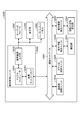
- FIG. 18 shows a first embodiment and its respective modifications, a second embodiment and its modifications, a third embodiment, and a use example using the image pickup apparatus 100 according to the fourth embodiment. It is a figure.
- the image pickup device 100 described above can be used in various cases where, for example, as shown below, light such as visible light, infrared light, ultraviolet light, and X-ray is sensed and recognition processing is performed based on the sensing result. ..
- -A device that captures images used for viewing, such as digital cameras and mobile devices with camera functions.
- in-vehicle sensors that photograph the front, rear, surroundings, inside of the vehicle, etc., monitoring cameras that monitor traveling vehicles and roads, inter-vehicle distance, etc.
- a device used for traffic such as a distance measuring sensor that measures the distance.
- -A device used for home appliances such as TVs, refrigerators, and air conditioners in order to take a picture of a user's gesture and operate the device according to the gesture.
- -Devices used for medical treatment and healthcare such as endoscopes and devices that perform angiography by receiving infrared light.
- -Devices used for security such as surveillance cameras for crime prevention and cameras for person authentication.
- -Apparatus used for beauty such as a skin measuring device that photographs the skin and a microscope that photographs the scalp.
- -Devices used for sports such as action cameras and wearable cameras for sports applications.
- -Agricultural equipment such as cameras for monitoring the condition of fields and crops.
- the technology according to the present disclosure (the present technology) can be applied to various products.
- the technology according to the present disclosure is realized as a device mounted on a moving body of any kind such as an automobile, an electric vehicle, a hybrid electric vehicle, a motorcycle, a bicycle, a personal mobility, an airplane, a drone, a ship, and a robot. You may.
- FIG. 19 is a block diagram showing a schematic configuration example of a vehicle control system, which is an example of a mobile control system to which the technique according to the present disclosure can be applied.
- the vehicle control system 12000 includes a plurality of electronic control units connected via the communication network 12001.
- the vehicle control system 12000 includes a drive system control unit 12010, a body system control unit 12020, an outside information detection unit 12030, an in-vehicle information detection unit 12040, and an integrated control unit 12050.
- a microcomputer 12051, an audio image output unit 12052, and an in-vehicle network I / F (interface) 12053 are shown as a functional configuration of the integrated control unit 12050.
- the drive system control unit 12010 controls the operation of the device related to the drive system of the vehicle according to various programs.
- the drive system control unit 12010 has a driving force generator for generating the driving force of the vehicle such as an internal combustion engine or a driving motor, a driving force transmission mechanism for transmitting the driving force to the wheels, and a steering angle of the vehicle. It functions as a control device such as a steering mechanism for adjusting and a braking device for generating braking force of the vehicle.
- the body system control unit 12020 controls the operation of various devices mounted on the vehicle body according to various programs.
- the body system control unit 12020 functions as a keyless entry system, a smart key system, a power window device, or a control device for various lamps such as headlamps, back lamps, brake lamps, turn signals or fog lamps.
- the body system control unit 12020 may be input with radio waves transmitted from a portable device that substitutes for the key or signals of various switches.
- the body system control unit 12020 receives inputs of these radio waves or signals and controls a vehicle door lock device, a power window device, a lamp, and the like.
- the vehicle outside information detection unit 12030 detects information outside the vehicle equipped with the vehicle control system 12000.
- the image pickup unit 12031 is connected to the vehicle outside information detection unit 12030.
- the vehicle outside information detection unit 12030 causes the image pickup unit 12031 to capture an image of the outside of the vehicle and receives the captured image.
- the out-of-vehicle information detection unit 12030 may perform object detection processing or distance detection processing such as a person, a vehicle, an obstacle, a sign, or a character on the road surface based on the received image.
- the image pickup unit 12031 is an optical sensor that receives light and outputs an electric signal according to the amount of the light received.
- the image pickup unit 12031 can output an electric signal as an image or can output it as distance measurement information. Further, the light received by the image pickup unit 12031 may be visible light or invisible light such as infrared light.
- the in-vehicle information detection unit 12040 detects the in-vehicle information.
- a driver state detection unit 12041 that detects the driver's state is connected to the in-vehicle information detection unit 12040.
- the driver state detection unit 12041 includes, for example, a camera that images the driver, and the in-vehicle information detection unit 12040 determines the degree of fatigue or concentration of the driver based on the detection information input from the driver state detection unit 12041. It may be calculated, or it may be determined whether the driver has fallen asleep.
- the microcomputer 12051 calculates the control target value of the driving force generator, the steering mechanism, or the braking device based on the information inside and outside the vehicle acquired by the vehicle exterior information detection unit 12030 or the vehicle interior information detection unit 12040, and the drive system control unit.
- a control command can be output to 12010.
- the microcomputer 12051 realizes ADAS (Advanced Driver Assistance System) functions including vehicle collision avoidance or impact mitigation, follow-up driving based on inter-vehicle distance, vehicle speed maintenance driving, vehicle collision warning, vehicle lane deviation warning, and the like. It is possible to perform cooperative control for the purpose of.
- ADAS Advanced Driver Assistance System
- the microcomputer 12051 controls the driving force generating device, the steering mechanism, the braking device, and the like based on the information around the vehicle acquired by the vehicle exterior information detection unit 12030 or the vehicle interior information detection unit 12040. It is possible to perform coordinated control for the purpose of automatic driving that runs autonomously without depending on the operation.
- the microcomputer 12051 can output a control command to the body system control unit 12020 based on the information outside the vehicle acquired by the vehicle outside information detection unit 12030.
- the microcomputer 12051 controls the headlamps according to the position of the preceding vehicle or the oncoming vehicle detected by the outside information detection unit 12030, and performs cooperative control for the purpose of anti-glare such as switching the high beam to the low beam. It can be carried out.
- the audio image output unit 12052 transmits an output signal of at least one of audio and image to an output device capable of visually or audibly notifying information to the passenger or the outside of the vehicle.
- an audio speaker 12061, a display unit 12062, and an instrument panel 12063 are exemplified as output devices.
- the display unit 12062 may include, for example, at least one of an onboard display and a head-up display.
- FIG. 20 is a diagram showing an example of the installation position of the image pickup unit 12031.
- the vehicle 12100 has an imaging unit 12101, 12102, 12103, 12104, 12105 as an imaging unit 12031.
- the image pickup units 12101, 12102, 12103, 12104, 12105 are provided, for example, at positions such as the front nose, side mirrors, rear bumpers, back doors, and the upper part of the windshield in the vehicle interior of the vehicle 12100.
- the image pickup unit 12101 provided in the front nose and the image pickup section 12105 provided in the upper part of the windshield in the vehicle interior mainly acquire an image in front of the vehicle 12100.
- the image pickup units 12102 and 12103 provided in the side mirror mainly acquire images of the side of the vehicle 12100.
- the image pickup unit 12104 provided in the rear bumper or the back door mainly acquires an image of the rear of the vehicle 12100.
- the images in front acquired by the image pickup units 12101 and 12105 are mainly used for detecting a preceding vehicle, a pedestrian, an obstacle, a traffic light, a traffic sign, a lane, or the like.
- FIG. 20 shows an example of the shooting range of the imaging units 12101 to 12104.
- the imaging range 12111 indicates the imaging range of the imaging unit 12101 provided on the front nose
- the imaging ranges 12112 and 12113 indicate the imaging range of the imaging units 12102 and 12103 provided on the side mirrors, respectively
- the imaging range 12114 indicates the imaging range.
- the imaging range of the imaging unit 12104 provided on the rear bumper or the back door is shown. For example, by superimposing the image data captured by the image pickup units 12101 to 12104, a bird's-eye view image of the vehicle 12100 can be obtained.
- At least one of the image pickup units 12101 to 12104 may have a function of acquiring distance information.
- at least one of the image pickup units 12101 to 12104 may be a stereo camera including a plurality of image pickup elements, or may be an image pickup element having pixels for phase difference detection.
- the microcomputer 12051 has a distance to each three-dimensional object in the image pickup range 12111 to 12114 based on the distance information obtained from the image pickup unit 12101 to 12104, and a temporal change of this distance (relative speed with respect to the vehicle 12100). By obtaining can. Further, the microcomputer 12051 can set an inter-vehicle distance to be secured in advance in front of the preceding vehicle, and can perform automatic brake control (including follow-up stop control), automatic acceleration control (including follow-up start control), and the like. In this way, it is possible to perform coordinated control for the purpose of automatic driving or the like in which the vehicle travels autonomously without depending on the operation of the driver.
- automatic brake control including follow-up stop control
- automatic acceleration control including follow-up start control
- the microcomputer 12051 converts three-dimensional object data related to a three-dimensional object into two-wheeled vehicles, ordinary vehicles, large vehicles, pedestrians, electric poles, and other three-dimensional objects based on the distance information obtained from the image pickup units 12101 to 12104. It can be classified and extracted and used for automatic avoidance of obstacles. For example, the microcomputer 12051 distinguishes obstacles around the vehicle 12100 into obstacles that are visible to the driver of the vehicle 12100 and obstacles that are difficult to see. Then, the microcomputer 12051 determines the collision risk indicating the risk of collision with each obstacle, and when the collision risk is equal to or higher than the set value and there is a possibility of collision, the microcomputer 12051 via the audio speaker 12061 or the display unit 12062. By outputting an alarm to the driver and performing forced deceleration and avoidance steering via the drive system control unit 12010, driving support for collision avoidance can be provided.
- At least one of the image pickup units 12101 to 12104 may be an infrared camera that detects infrared rays.
- the microcomputer 12051 can recognize a pedestrian by determining whether or not a pedestrian is present in the captured image of the imaging unit 12101 to 12104.
- pedestrian recognition is, for example, a procedure for extracting feature points in an image captured by an image pickup unit 12101 to 12104 as an infrared camera, and pattern matching processing is performed on a series of feature points indicating the outline of an object to determine whether or not the pedestrian is a pedestrian. It is done by the procedure to determine.
- the audio image output unit 12052 determines the square contour line for emphasizing the recognized pedestrian.
- the display unit 12062 is controlled so as to superimpose and display. Further, the audio image output unit 12052 may control the display unit 12062 so as to display an icon or the like indicating a pedestrian at a desired position.
- the above is an example of a vehicle control system to which the technology according to the present disclosure can be applied.
- the technique according to the present disclosure can be applied to the image pickup unit 12031 and the vehicle exterior information detection unit 12030 among the configurations described above.
- the technique according to the present disclosure to the imaging unit 12031 and the vehicle exterior information detection unit 12030, it is possible to appropriately perform imaging even in an environment with a large amount of light.
- the present technology can also have the following configurations.
- a generator that generates a voltage according to the logarithmic value of the photocurrent, A capacitor in which the voltage generated by the generation unit is applied to the first electrode, The second electrode of the capacitor is connected to the first input end, the first reference voltage is applied to the second input end, the voltage applied to the first input end and the second input end.
- a first amplifier that outputs a comparison result comparing with the voltage applied to A switch unit that controls the connection between the output of the first amplifier and the first input end, and The output of the first amplifier is connected to the third input end, the second reference voltage is applied to the fourth input end, the voltage applied to the third input end and the fourth input end.
- a second amplifier that outputs a comparison result comparing with the voltage applied to Equipped with a pixel circuit with The first gain of the first amplifier is lower than the second gain of the second amplifier.
- Solid-state image sensor. (2) The first amplifier has a first gain changing unit that changes the first gain. The solid-state image sensor according to (1) above. (3) The first gain changing unit changes the first gain by changing the first reference voltage. The solid-state image sensor according to (2) above. (4) The first gain changing unit changes the first gain by changing the elements constituting the first amplifier. The solid-state image sensor according to (2) above. (5) The element is a transistor to which a voltage is applied from the first input end in the first amplifier. The first gain changing unit changes the first gain by changing the number of connections in which the transistors are connected in parallel.
- the element is a capacitor for applying negative feedback to the first amplifier.
- the first gain changing unit changes the first gain by changing the capacitance of the capacitor.
- the element is a resistor for applying negative feedback to the first amplifier.
- the first gain changing unit changes the first gain by changing the resistance value of the resistor.
- the second amplifier has a second gain changer that changes the second gain.
- the second gain changing unit changes the second gain by changing the second reference voltage.
- the second gain changing unit changes the second gain by switching the elements constituting the second amplifier.
- the element is a transistor to which a voltage is applied from the third input end in the second amplifier.
- the second gain changing unit changes the second gain by changing the number of connections in which the transistors are connected in parallel.
- the pixel circuits are arranged in a matrix arrangement to form a pixel array.
- the second amplifier is shared by two or more pixel circuits among the pixel circuits included in the pixel array.
- the first amplifier is shared by two or more of the second amplifiers.
- a voltage generated according to the logarithmic value of the photocurrent is applied to the first electrode of the capacitor.
- the second electrode of the capacitor is connected to the first input end, the first reference voltage is applied to the second input end, and the connection between the output and the first input end is controlled by the switch unit.
- the first amplifier is output a comparison result comparing the voltage applied to the first input end and the voltage applied to the second input end.
- the output of the first amplifier is connected to the third input end, and the second reference voltage is applied to the fourth input end.
- the second amplifier has the voltage applied to the third input end.
- a comparison result comparing with the voltage applied to the fourth input end is output.
- the first gain of the first amplifier is lower than the second gain of the second amplifier. Imaging method.
- a generator that generates a voltage according to the logarithmic value of the photocurrent, A capacitor in which the voltage generated by the generation unit is applied to the first electrode, The second electrode of the capacitor is connected to the first input end, the first reference voltage is applied to the second input end, the voltage applied to the first input end and the second input end.
- a first amplifier that outputs a first comparison result comparing with the voltage applied to the A switch unit that controls the connection between the output of the first amplifier and the first input end, and The output of the first amplifier is connected to the third input end, the second reference voltage is applied to the fourth input end, the voltage applied to the third input end and the fourth input end.
- a second amplifier that outputs a second comparison result comparing with the voltage applied to the With a pixel circuit with A recording unit that records a signal based on the second comparison result, and a recording unit. Equipped with The gain of the first amplifier is lower than the gain of the second amplifier. Electronics.
- Detection circuit 40a 40a 1 , 40a 2 , 40b, 41a, 41b, 41 ON , 41 OFF , 3400 Comparator 42, 43, 44, 45, 46, 47 1 , 47 2
Landscapes
- Engineering & Computer Science (AREA)
- Multimedia (AREA)
- Signal Processing (AREA)
- Power Engineering (AREA)
- Transforming Light Signals Into Electric Signals (AREA)
Abstract
本開示に係る固体撮像装置は、光電流の対数値に応じた電圧を生成する生成部(31)と、生成部で生成された電圧が第1の電極に印加されるコンデンサ(C1)と、第1の入力端にコンデンサの第2の電極が接続され、第2の入力端に第1の参照電圧(VbA0)が印加され、第1の入力端に印加された電圧と第2の入力端に印加された電圧とを比較した比較結果を出力する第1の増幅器(40a)と、第1の増幅器の出力と第1の入力端との間の接続を制御するスイッチ部(43)と、第3の入力端に第1の増幅器の出力が接続され、第4の入力端に第2の参照電圧(VbA1)が印加され、第3の入力端に印加された電圧と第4の入力端に印加された電圧とを比較した比較結果を出力する第2の増幅器(40b)と、を有する画素回路を備え、第1の増幅器の第1のゲインは、第2の増幅器の第2のゲインより低くされる。
Description
本開示は、固体撮像装置、撮像方法および電子機器に関する。
CMOS(Complementary Metal Oxide Semiconductor)などを用いた固体撮像装置において、画素アドレス毎に、その画素が受光した光量が閾値を超えた旨をアドレスイベントとしてリアルタイムに検出する検出回路を画素毎に設けた、非同期型の固体撮像素子が知られている。このように、画素毎にアドレスイベントを検出する固体撮像素子は、DVS(Dynamic Vision Sensor)と呼ばれる。
このようなDVSの構成として、光電変換素子から出力された光電流を対数の電圧信号に変換し、この電圧信号をコンパレータにて閾値と比較してアドレスイベントの検出を行う構成が提案されている。この構成によれば、コンパレータにおける閾値を制御することで、DVSのコントラスト感度を調整できる。
DVSにおいて、例えばダイナミックレンジを広げるため、コントラスト感度を低くしたい場合がある。上述のように、コンパレータに対する閾値を制御することで、コントラスト感度を低くすることが可能である。しかしながら、コンパレータ自体のゲインが高いと、閾値の設定可能な電圧の範囲に、コントラスト感度の制御範囲が制限されてしまう。
本開示は、より広いダイナミックレンジでの撮像が可能な固体撮像素子、撮像方法および電子機器を提供することを目的とする。
本開示に係る固体撮像装置は、光電流の対数値に応じた電圧を生成する生成部と、生成部で生成された電圧が第1の電極に印加されるコンデンサと、第1の入力端にコンデンサの第2の電極が接続され、第2の入力端に第1の参照電圧が印加され、第1の入力端に印加された電圧と第2の入力端に印加された電圧とを比較した比較結果を出力する第1の増幅器と、第1の増幅器の出力と第1の入力端との間の接続を制御するスイッチ部と、第3の入力端に第1の増幅器の出力が接続され、第4の入力端に第2の参照電圧が印加され、第3の入力端に印加された電圧と第4の入力端に印加された電圧とを比較した比較結果を出力する第2の増幅器と、を有する画素回路を備え、第1の増幅器の第1のゲインは、第2の増幅器の第2のゲインより低くされる。
以下、本開示の実施形態について、図面に基づいて詳細に説明する。なお、以下の実施形態において、同一の部位には同一の符号を付することにより、重複する説明を省略する。
以下、本開示の実施形態について、下記の順序に従って説明する。
1.各実施形態に適用可能な技術
2.本開示に係る実施形態の概要
3.第1の実施形態
3-1.第1の実施形態の第1の変形例
3-2.第1の実施形態の第2の変形例
3-3.第1の実施形態の第3の変形例
4.第2の実施形態
4-1.第2の実施形態の変形例
5.第3の実施形態
6.第4の実施形態
7.第5の実施形態
7-1.本開示の技術の適用例
7-2.移動体への適用例
1.各実施形態に適用可能な技術
2.本開示に係る実施形態の概要
3.第1の実施形態
3-1.第1の実施形態の第1の変形例
3-2.第1の実施形態の第2の変形例
3-3.第1の実施形態の第3の変形例
4.第2の実施形態
4-1.第2の実施形態の変形例
5.第3の実施形態
6.第4の実施形態
7.第5の実施形態
7-1.本開示の技術の適用例
7-2.移動体への適用例
[1.各実施形態に適用可能な技術]
先ず、本開示の各実施形態に適用可能な技術について説明する。図1は、各実施形態に適用可能な電子機器としての撮像装置の一例の構成を示すブロック図である。図1において、撮像装置100は、光学部110と、固体撮像素子200と、記録部120と、制御部130と、を備える。撮像装置100としては、産業用ロボットに搭載されるカメラや、車載カメラなどが想定される。
先ず、本開示の各実施形態に適用可能な技術について説明する。図1は、各実施形態に適用可能な電子機器としての撮像装置の一例の構成を示すブロック図である。図1において、撮像装置100は、光学部110と、固体撮像素子200と、記録部120と、制御部130と、を備える。撮像装置100としては、産業用ロボットに搭載されるカメラや、車載カメラなどが想定される。
光学部110は、入射光を集光して固体撮像素子200に導く。固体撮像素子200は、入射光を光電変換して画素信号を出力する撮像動作を行う。固体撮像素子200は、入射光に基づく画素信号に基づき、画像認識処理など所定の信号処理を施して出力データを生成し、生成した出力データを、信号線209を介して記録部120に供給する。
記録部120は、固体撮像素子200から供給された出力データを記録する。制御部130は、例えば所定のプログラムに従い、固体撮像素子200の撮像動作や記録部120における記録動作を制御する。
図2は、各実施形態に適用可能な固体撮像素子200の構造の例を示す模式図である。固体撮像素子200は、図2に模式的に示すように、検出チップ202と、その検出チップ202に積層された受光チップ201と、による積層構造を有する。受光チップ201および検出チップ202は、ビアなどの接続部を介して電気的に接続される。受光チップ201および検出チップ202の接続方法は、ビアに限らず、Cu-Cu接合やバンプを適用することもできる。
図3は、各実施形態に適用可能な受光チップ201の一例の平面図である。受光チップ201には、受光部220と、ビア配置部211、212および213と、が設けられる。
ビア配置部211、212および213は、検出チップ202と接続されるビアが配置される。また、受光部220には、行列状の配列で複数の共有ブロック221が配置される。
共有ブロック221のそれぞれには、複数の受光回路31が行列状に配置される。図3の例では、共有ブロック221毎に、4つの受光回路31が2行×2列で配置される。これらの4つの受光回路31は、検出チップ202上の回路を共有する。共有する回路の詳細については後述する。なお、共有ブロック221内の受光回路31の個数は、4つに限定されない。例えば、共有ブロック221内に、2乃至3個の受光回路31が配置されてもよいし、5以上の受光回路31が配置されてもよい。さらには、共有ブロック221に1つの受光回路31のみが配置されてもよい。
受光回路31は、光電変換素子と、対数応答により光電変換素子から出力される光電流をその対数値に応じた電圧信号を生成する対数応答回路と、対数応答回路により生成された電圧信号の変化量を検出する検出回路と、を含む。受光回路31のそれぞれには、行アドレスおよび列アドレスからなる画素アドレスが割り当てられている。
図4は、各実施形態に適用可能な検出チップ202の一例の平面図である。図4の例では、検出チップ202は、ビア配置部231、232および233と、信号処理回路240と、行駆動回路251と、列駆動回路252と、アドレスイベント検出部260と、が設けられる。ビア配置部231、232および233には、受光チップ201の各ビア配置部211、212および213と接続されるビアが配置される。
アドレスイベント検出部260は、受光回路31毎にアドレスイベントの有無を検出し、検出結果を示す検出信号を生成する。
行駆動回路251は、行アドレスを選択して、その行アドレスに対応する検出信号をアドレスイベント検出部260に出力させる。列駆動回路252は、列アドレスを選択して、その列アドレスに対応する検出信号をアドレスイベント検出部260に出力させる。
信号処理回路240は、アドレスイベント検出部260からの検出信号に対して所定の信号処理を実行する。この信号処理回路240は、検出信号を画素の信号として2次元格子状すなわち行列状の配列で配置し、画素毎に2ビットの情報を有する画像データを取得する。そして、信号処理回路240は、その画像データに対して画像認識処理などの信号処理を実行する。
図5は、各実施形態に適用可能なアドレスイベント検出部260の一例の平面図である。図5において、アドレスイベント検出部260は、複数の検出ブロック32が配列される。検出ブロック32は、受光チップ201上の共有ブロック221毎に配置される。共有ブロック221の個数がN(Nは、整数)である場合、N個の検出ブロック32が配列される。それぞれの検出ブロック32は、対応する共有ブロック221と接続される。
図6は、各実施形態に適用可能な受光回路31および検出ブロック32の一例の構成を示す図である。受光回路31の出力が検出ブロック32に供給される。検出ブロック32は、バッファ33と、検出回路34と、を含む。
図6において、受光回路31は、光電変換素子310と、nMOS(n-channel MetalOxide Semiconductor)トランジスタであるによるトランジスタ311a、311b、312aおよび312bと、pMOS(p-channel MOS)トランジスタであるトランジスタ313と、を備える。これらのうち、光電変換素子310と、トランジスタ311a、311b、312aおよび312bとは、例えば、受光チップ201に配置され、トランジスタ313は、検出チップ202に配置される。
光電変換素子310は、受光に応じた光電流Iphtを出力する。
トランジスタ311bは、ソースが光電変換素子310のカソードに接続され、ドレインがトランジスタ311aのソースに接続される。トランジスタ311aのドレインは、電源端子Vddに接続される。光電変換素子311のアノードは、接地端子に接続される。
光電変換素子310のカソードとトランジスタ311bのドレインとの接続点に、トランジスタ312bのゲートが接続される。トランジスタ312bは、ソースが接地端子に接続され、ドレインがトランジスタ312aのソースに接続される。トランジスタ312bのドレインと、トランジスタ312aのソースとの接続点に、トランジスタ311bのゲートが接続される。トランジスタ312aのドレインがトランジスタ313のソースに接続される。トランジスタ313は、ドレインが電源端子Vddに接続され、ゲートに所定のバイアス電圧Vbiasが印加される。トランジスタ311aのゲートが、トランジスタ312aのドレインと、トランジスタ313のソースとの接続点に接続される。
トランジスタ311bおよび312bのドレインは、それぞれ電源側に接続されており、それぞれソースフォロワ回路を形成している。これらトランジスタ311bおよび312bによる2つのソースフォロワ回路は、ループ状に接続されている。同様に、トランジスタ311aおよび312aのそれぞれは、ドレインが電源側に接続されソースフォロワ回路を形成し、これらトランジスタ311aおよび312aによる2つのソースフォロワ回路は、ループ状に接続されている。すなわち、図6に示す受光回路31は、2つのソースフォロワ回路がループ状に接続された回路が直列接続された構成を含む。
光電変換素子310から出力された光電流Iphtは、この2つのソースフォロワ回路がループ状に接続された回路が直列接続された構成により、その対数値に応じた電圧信号に変換される。また、トランジスタ313は、一定の電流をトランジスタ312aおよび312bに供給する。このように、受光回路31は、光電流の対数値に応じた電圧を生成する生成部として機能する。
なお、受光チップ201のグランドと検出チップ202のグランドとは、干渉対策のために互いに分離されている。
受光回路31において、光電流Iphtがその対数値に応じて変換された電圧信号は、トランジスタ313のソースとトランジスタ312aのドレインとの接続点から取り出され、それぞれnMOSトランジスタであるトランジスタ331および332を含むバッファ33を介して、電圧信号Vpdとして検出回路34に入力される。
検出回路34は、検出部340aと、メモリ341と、転送回路342と、を含む。図6の例では、検出部340aは、例えば行駆動回路251からリセット信号RSTと、閾値電圧Vbとが供給される。検出部340aは、受光回路31からバッファ33を介して入力される電圧信号Vpdに対して閾値Vthに基づく判定処理を行い、光電変換素子310における受光量の変化を示す信号Vcompを出力する。信号Vcompは、受光量の正(+)方向の変化を示す信号VONと、負(-)方向の変化を示す信号VOFFと、を含むもので、アドレスイベントの発生を示す。
図7は、既存技術による検出部340aの構成の例を示す図である。ここでは、既存技術による検出部340aとして、特許文献1のFig.1に示される構成を適用している。図7において、検出部340aaは、コンデンサC1と、コンパレータ3400と、リセット回路3401と、を含む。
コンデンサC1は、第1の電極に電圧信号Vpdが供給され、光電変換素子310により、受光に応じて生成された電荷がコンデンサC1に供給される。コンデンサC1の第2の電極は、コンパレータ3400の反転入力端(-)に接続される。コンパレータ3400の反転入力端(-)に入力される信号は、コンデンサC1の第1の電極に入力される電圧信号Vpdの変化に応じて変化する信号Vdiffとなる。
コンパレータ3400の非反転入力端(+)に対して、行駆動回路251から供給される閾値電圧Vbが入力される。
コンパレータ3400から出力された信号Vcompがメモリ341に供給され、記憶される。メモリ341は、サンプリング回路により構成される。サンプリング回路は、例えば、スイッチとコンデンサとを用いて実現できる。これに限らず、メモリ341をラッチ回路やフリップフロップ回路といったメモリ回路により構成してもよい。
コンデンサC1の第2の電極と、コンパレータ3400の反転入力端(-)との接続点に、リセット回路3401が接続される。リセット回路3401は、行駆動回路251からリセット信号RSTが供給される。リセット信号RSTは、リセット回路3401をアクティブにする時間を選択するための信号である。行駆動回路251は、メモリ341に記憶される信号Vcompに応じて、リセット信号RSTを出力する。
リセット回路3401は、リセット信号RSTによりアクティブにされることで、コンデンサC1の第2の電極の状態をリセットする。したがって、コンデンサC1の第2の電極は、現在の電圧信号Vpdと、過去の電圧信号Vpdとの差分の信号Vdiffが現れる。コンパレータ3400は、この信号Vdiffの電圧と閾値電圧Vbとを比較し、比較結果として信号Vcompを出力する。
説明を図6に戻し、転送回路342は、例えば制御部130の制御に従い列駆動回路252から供給される列駆動信号に応じて、メモリ341から信号Vcompを読み出し、読み出した信号Vcompを、検出ブロック32によるアドレスイベントの検出結果を示す検出出力として検出ブロック32から出力する。この検出出力は、例えば信号処理回路240に供給される。信号処理回路240は、検出ブロック32から供給された検出出力に基づき、画像認識処理など所定の信号処理を施す。信号処理回路240で所定の信号処理を施された検出出力は、例えば記録部120に記録される。これに限らず、記録部120に対して、検出ブロック32からの検出出力を直接的に記録してもよい。
既存技術によるコンパレータ3400の動作について、より詳細に説明する。コンパレータ3400は、光電変換素子310に受光された光量が増加したイベントと、減少したイベントと、を検出する。以下、光量が増加したイベントを(+)イベント、光量が減少したイベントを(-)イベントと呼ぶ。
(-)イベントを検出する場合、行駆動回路251は、例えば制御部130の制御に従い、電圧Voffの閾値電圧Vbを出力し、コンパレータ3400に供給する。一方、(+)イベントを検出する場合、行駆動回路251は、例えば制御部130の制御に従い、電圧Voffより低い電圧Vonの閾値電圧Vbを出力し、コンパレータ3400に供給する。行駆動回路251は、例えば、電圧Voff、電圧Vonおよび電圧Vresetを時系列上で繰り返して閾値電圧Vbとして出力する。なお、電圧Vresetは、例えば電圧Voffと電圧Vonとの中間の電圧値とされる。
(-)イベントを検出する場合、コンパレータ3400は、信号Vdiffの電圧が、電圧Voffである閾値電圧Vb未満の場合、信号Vcompがハイ(High)レベルとなり、この信号Vcompがメモリ341に記憶される。これは、(-)イベントすなわち光量の減少が検出されたことを示す。若し、信号Vdiffの電圧が閾値電圧Vb(電圧Voff)以上である場合、コンパレータ3400から出力される信号Vcompはロー(Low)レベルとなり、光量の減少が検出されなかったことを示す。
一方、(+)イベントを検出する場合、コンパレータ3400は、信号Vdiffの電圧が、電圧Vonである閾値電圧Vbを超える場合、信号Vcompがローレベルとなり、この信号Vcompがメモリ341に記憶される。これは、(+)イベントすなわち光量の増加が検出されたことを示す。若し、信号Vdiffの電圧が閾値電圧Vb(電圧Von)以下である場合、コンパレータ3400から出力される信号Vcompはハイレベルとなり、光量の増加が検出されなかったことを示す。
したがって、メモリ341から信号Vcompを読み出す際には、メモリ341の内容と、閾値電圧Vbとして電圧VoffおよびVonの何れが適用されたかを知る必要がある。例えば、制御部130は、行駆動回路251を介してメモリ341の内容を取得し、取得したメモリ341の内容と、閾値電圧Vbとに基づき、列駆動回路252に対して、メモリ341からの信号Vcompの読み出しを指示する。
既存技術による受光回路31および検出ブロック32の動作について、より具体的に説明する。光電変換素子310に受光された光量の変化は、受光回路31に含まれる対数変換回路により電圧信号Vpdの変化に変換される。リセット回路3401がアクティブではなく導通していない場合、電圧信号Vpdの変化は、コンデンサC1を介してコンパレータ3400の反転入力端(-)に入力される信号Vdiffに反映される。これは、コンデンサC1の両端の電圧が一定電圧に留まるためである。
コンパレータ3400は、行駆動回路251により選択された際に、コンデンサC1の第2の電極における、反転入力端(-)に入力される信号Vdiffの電圧と、非反転入力端(+)に印加される閾値電圧Vbとを比較する。コンパレータ3400は、比較結果として信号Vcompを出力する。コンパレータ3400から出力された信号Vcompは、例えば行駆動回路251によりメモリ341に記憶される。
行駆動回路251は、メモリ341の記憶内容および閾値電圧Vbに基づき、メモリ341に記憶される信号Vcompが光電変換素子310に受光された光量の変化を示していると判定され、且つ、リセット信号RSTがアクティブである場合、リセット回路3401を導通させる。リセット回路3401が導通状態になると、コンパレータ3400の反転入力端(-)における信号Vdiffの電圧が既知のレベルにリセットされる。そのため、コンデンサC1に対して、現在の電圧信号Vpdが格納される。
[2.本開示に係る実施形態の概要]
次に、本開示の実施形態の概要について説明する。上述した既存技術による構成において、例えばDVSのダイナミックレンジを広げるため、コントラスト感度を低くしたい場合がある。この場合、コンパレータ3400に印加する閾値電圧Vbを制御することで、コントラスト感度を低くすることが可能である。しかしながら、コンパレータ3400自体のゲインが高いと、閾値電圧Vbの設定可能な電圧の範囲に、コントラスト感度の制御範囲が制限されてしまう。
次に、本開示の実施形態の概要について説明する。上述した既存技術による構成において、例えばDVSのダイナミックレンジを広げるため、コントラスト感度を低くしたい場合がある。この場合、コンパレータ3400に印加する閾値電圧Vbを制御することで、コントラスト感度を低くすることが可能である。しかしながら、コンパレータ3400自体のゲインが高いと、閾値電圧Vbの設定可能な電圧の範囲に、コントラスト感度の制御範囲が制限されてしまう。
そこで、本開示に係る実施形態では、DVS回路におけるコンパレータを2段接続とし、入力側のコンパレータのゲインを、出力側のコンパレータのゲインに対して低く設定する。これにより、入力側のコンパレータに入力可能な電圧信号Vpdの範囲を広げることができ、DVS回路の低コントラスト化が可能となる。
[3.第1の実施形態]
次に、本開示の第1の実施形態について説明する。図8Aは、第1の実施形態に係る検出部340bの構成の例を示す図である。図8Aにおいて、検出部340bは、コンデンサC1と、それぞれ増幅器としての構成を有する、直列に接続されるコンパレータ40aおよび41aと、スイッチ回路42および43と、を含む。
次に、本開示の第1の実施形態について説明する。図8Aは、第1の実施形態に係る検出部340bの構成の例を示す図である。図8Aにおいて、検出部340bは、コンデンサC1と、それぞれ増幅器としての構成を有する、直列に接続されるコンパレータ40aおよび41aと、スイッチ回路42および43と、を含む。
コンデンサC1の第1の電極には、受光回路31から出力された電圧信号Vpdが、バッファ33を介して印加され、第2の電極から信号Vdiffが入力側の増幅器である第1の増幅器としてのコンパレータ40aの第1の入力端である反転入力端(-)に入力される。コンパレータ40aの第2の入力端である非反転入力端(+)には、スイッチ回路42の選択出力端が接続される。
図8Aの例では、スイッチ回路42は、3つの選択入力端42a、42bおよび42cを含む。これら選択入力端42a、42bおよび42cは、それぞれ電圧Vaz、VbonおよびVboffが印加される。電圧Vbonは、(+)イベントを判定するための閾値である。電圧Vboffは、(-)イベントを判定するための閾値である。また、電圧Vazは、例えば電圧Vbonと電圧Vboffとの中間の電圧であり、直前に検出されたイベントをリセットするためのリセットレベルの電圧である。
スイッチ回路42は、例えば行駆動回路251からの制御信号(図示しない)に従い、選択入力端42a、42bおよび42cのうち何れかの入力端が選択され、選択された入力端に印加される電圧が第1の参照電圧信号である閾値電圧VbA0として、コンパレータ40aの非反転入力端(+)に印加される。
例えば、閾値電圧VbA00として電圧Vbonが選択されている場合、コンパレータ40aの反転入力端(-)に印加された信号Vdiffの電圧が、電圧Vazから電圧Vbonの方向に向けて、電圧Vbonを超えた場合に、(+)イベントが検出される。また、閾値電圧VbA0として電圧Vboffが選択されている場合、当該信号Vdiffの電圧が、電圧Vazから電圧Vboffの方向に向けて、電圧Vboffを超えた場合に、(-)イベントが検出される。一方、信号Vdiffの電圧が、電圧Vazから電圧Vbonの方向に向けて、電圧Vbonを超えず、且つ、電圧Vazから電圧Vboffの方向に向けて、電圧Vboffを超えない場合は、(+)イベントおよび(-)イベントが何れも検出されない。
以下、特に記載の無い限り、「信号Vdiffの電圧が、電圧Vazから電圧Vbonの方向に向けて、電圧Vbonを超えた」ことを、「信号Vdiffの電圧が電圧Vbonを超えた」とし、同様に「信号Vdiffの電圧が、電圧Vazから電圧Vboffの方向に向けて、電圧Vboffを超えた」ことを、「信号Vdiffの電圧が電圧Vboffを超えた」などとして説明を行う。また、「信号Vdiffの電圧が電圧Vbonを超えた」、および、「信号Vdiffの電圧が電圧Vboffを超えた」ことを、纏めて「信号Vdiffの電圧が閾値電圧VbA0を超えた」とすることがある。
第1の実施形態では、これら電圧VbonおよびVboffが電圧値を可変とされている。例えば、電圧VbonおよびVboffの電圧値の、電圧Vazとの差分の絶対値が大きいほど、光量変化の検出感度(コントラスト感度)が低くなる。これは、すなわち、コンパレータ40aのゲインを低くしたことに相当する。このように、電圧VbonおよびVboffは、コンパレータ40aのゲインを変更するゲイン変更部として機能する。
一例として、より光量の多い環境での使用の際には、電圧VbonおよびVboffを、電圧Vazとの差分の絶対値がより大きい電圧値に切り替えることが考えられる。
スイッチ回路42において、電圧Vbon、VboffおよびVazの何れかが選択された出力は、閾値電圧VbA00としてコンパレータ40aの反転入力端(-)に印加される。コンパレータ40aは、非反転入力端(+)に印加された閾値電圧VbA0と、反転入力端(-)に入力された信号Vdiffの電圧とを比較し、比較結果として信号Vcomp1を出力する。
コンパレータ40aの出力端は、出力側の増幅器である第2の増幅器としてのコンパレータ41aの第3の入力端子としての反転入力端(-)に接続されると共に、スイッチ回路43の一端に接続される。スイッチ回路43の他端は、コンデンサC1の第2の電極とコンパレータ40aの反転入力端(-)との接続点に接続される。スイッチ回路43は、図7に示したリセット回路3401に対応するもので、例えば行駆動回路251からの制御信号(図示しない)により導通/非導通状態を制御される。スイッチ回路43が導通状態で、コンデンサC1の電圧が、コンパレータ40aが直前に出力した信号Vcompにリセットされる。
コンパレータ41aは、第4の入力端子としての非反転入力端(+)に、第2の参照電圧としての所定の閾値電圧VbA1が印加される。コンパレータ41aは、反転入力端(-)に印加される信号Vcomp1と、非反転入力端(+)に入力される閾値電圧VbA1とを比較し、比較結果を示す信号Vcomp2を出力する。この信号Vcomp2は、検出部340aから出力され、メモリ341に記憶される。
図8Bは、第1の実施形態に係る検出部340bの構成の例を示す回路図である。図8Bにおいて、コンパレータ40aは、pMOSトランジスタであるトランジスタ401と、nMOSトランジスタであるトランジスタ402と、を含む。また、この例では、スイッチ回路43がnMOSトランジスタにより構成されている。
トランジスタ401は、ソースが電源端子Vddに接続され、ドレインがトランジスタ402のドレインに接続される。トランジスタ402のソースは、接地端子に接続される。トランジスタ401のドレインと、トランジスタ402のドレインとの接続点から、このコンパレータ40aの出力である信号Vcomp1が取り出される。また、当該接続点に対して、スイッチ回路43の一端(nMOSトランジスタの例えばドレイン)が接続される。トランジスタ401のゲートに、コンデンサC1の第2の電極が接続され、トランジスタ401のゲートとコンデンサC1との接続点に、スイッチ回路43の他端(nMOSトランジスタの例えばソース)が接続される。
コンパレータ41aは、pMOSトランジスタであるトランジスタ411と、nMOSトランジスタであるトランジスタ412と、を含む。トランジスタ411のソースが電源端子Vddに接続され、ドレインがトランジスタ412のドレインに接続される。トランジスタ412のソースが接地端子に接続される。
コンパレータ40aにおけるトランジスタ401のドレインと、トランジスタ402のドレインと、の接続点がコンパレータ41aにおけるトランジスタ411のゲートに接続される。すなわち、当該接続点から取り出されたコンパレータ40aの出力である信号Vcomp1が、トランジスタ411のゲートに印加される。トランジスタ412のゲートには、所定の閾値電圧VbA1が印加される。トランジスタ411のドレインと、トランジスタ412のドレインと、の接続点から、コンパレータ41aの出力である信号Vcomp2が取り出される。
このような構成において、コンパレータ40aは、トランジスタ401のゲートに印加された信号Vdiffの電圧と、トランジスタ402のゲートに印加された閾値電圧VbA0と、を比較する。コンパレータ40aは、比較の結果、信号Vdiffの電圧が閾値電圧VbA0を超えた場合に、コンパレータ40aの出力である信号Vcomp1の状態を、例えばハイレベルからローレベルに遷移させる。
コンパレータ40aによる比較動作について説明する。nMOSトランジスタであるトランジスタ402のゲートに閾値電圧VbA0(電圧Vbon、VboffおよびVazの何れか)が印加されている場合、当該トランジスタ402のドレインには、ゲートに印加される電圧に応じたドレイン電流Idsnが流れる。また、pMOSトランジスタであるトランジスタ401のゲートにある電圧(電圧Vdiff)が印加されている場合に当該トランジスタ401にドレイン電流Idspが流れるものとする。ここで、[電流Idsn>電流Idsp]であれば、トランジスタ402の方が電流が大きいことにより、出力電圧の電位が接地電位側に下がり、出力される信号Vcomp1がローレベルとなる。一方、[電流Idsn<電流Idsp]であれば、トランジスタ401の電流の方が多くなることで、電源側に出力電位が持ち上がり、信号Vcomp1がハイレベルとなる。このようにして、コンパレータ40aにおいて、トランジスタ401のゲートに印加される信号Vdiffと、トランジスタ402のゲートに印加される閾値電圧VbA0との比較動作が行われる。
コンパレータ41aは、コンパレータ40aの出力である信号Vcomp1を、トランジスタ412のゲートに印加される閾値電圧VbA1と比較する。コンパレータ41aは、信号Vcomp1が閾値電圧VbA1を超えた場合に、コンパレータ41aの出力である信号Vcomp2の状態を、例えばローレベルからハイレベルに遷移させる。
ここで、上述したように、nMOSトランジスタであるトランジスタ402のゲート電位により、当該トランジスタ402のドレイン電流Idsnが変化する。その際に、当該ドレイン電流Idsnと釣り合う、pMOSトランジスタであるトランジスタ401におけるドレイン電流Idspも変化する。その際に、トランジスタ401のゲートに印加される電位もまた、変化することになり、トランジスタ401からは、閾値が変化して見えることになる。このとき、閾値までに必要なトランジスタ401のゲート電位の変化量が大となる方向への閾値電圧VbonおよびVboffの変化は、コンパレータ40aの反転能力が小さくなったように見え、コンパレータ40aのゲインを下げることと等価であると考えることができる。
ここで、コンパレータ40aは、反転入力端(-)に入力された信号Vdiffに対する、閾値電圧Vba0による閾値判定を、コンパレータ41aにおける閾値判定と比較して緩やかに実行するように構成される。すなわち、コンパレータ40aは、反転入力端(-)に入力された電圧(信号Vdiff)が閾値電圧VbA0を超えた場合の信号Vcomp1の立ち下がり(あるいは立ち上がり)の速度が、コンパレータ41aにおいて反転入力端(-)に入力された電圧(信号Vcomp1)が閾値電圧VbA1を超えた場合の信号Vcomp2の立ち上がり(あるいは立ち下がり)の速度よりも、遅くなるようにする。
なお、図8Bでは、トランジスタ401および411をそれぞれpMOSトランジスタとし、トランジスタ402および412をそれぞれnMOSトランジスタとしているが、これはこの例に限定されない。例えば、トランジスタ401および411をそれぞれnMOSトランジスタとし、トランジスタ402および412をそれぞれpMOSトランジスタとしてもよい。
図9は、第1の実施形態に係る検出部340bの動作を説明するための模式図である。図9のセクション(a)および(b)それぞれにおいて、横軸は時間、縦軸は、それぞれの電圧を示している。
図9のセクション(a)は、図7を用いて説明した、既存技術による検出部340aの動作の例を示している。このセクション(a)の上段は、コンデンサC1の第1の電極に印加される電圧信号Vpdを示し、下段は、コンパレータ3400から出力される信号Vcompを示している。また、ここでは、光量が増加した(+)イベントについて示している。
図において、電圧信号Vpdは、例えば時間t10から上昇を開始しているものとする。コンパレータ3400は、時間t10においては、ハイ状態の信号Vcompを出力している。コンパレータ3400は、電圧信号Vpdが閾値電圧Vb以下の場合は、ハイ状態の電圧Vcompを出力する。電圧信号Vpdが時間t12で閾値電圧Vbを超えたものとする。コンパレータ3400において、時間t11の手前の時間t11から信号Vcompの立ち下がりが開始され、時間t13において、信号Vcompの立ち下がりが完了し、信号Vcompがロー状態に遷移される。
図9のセクション(b)は、図8Aおよび図8Bを用いて説明した、第1の実施形態に係る検出部340bの動作の例を示している。上述と同様に、このセクション(b)の上段は、コンデンサC1の第1の電極に印加される電圧信号Vpdを示し、中段は、コンパレータ40aから出力される信号Vcomp1を示し、さらに下段は、コンパレータ41aから出力される信号Vcomp2を示している。なお、セクション(b)の上段の電圧信号Vpdの変化は、セクション(a)の上段における電圧信号Vpdの変化と同一である。また、コンパレータ40aにおける閾値電圧VbA0は、コンパレータ3400における閾値電圧Vbと同一であるものとする。
図において、電圧信号Vpdは、例えば時間t20(上述の時間t10と対応)から上昇を開始しているものとする。コンパレータ40aは、電圧信号Vpdが閾値電圧Vb以下の場合は、ハイ状態の信号Vcomp1を出力する。電圧信号Vpdが時間t21で閾値電圧VbA0を超えたものとする。なお、電圧信号Vpdの上昇の傾きは、図9のセクション(a)における傾きと同一であり、時間t20~t21の時間は、上述の時間t10~t11の時間と同じであるものとする。
コンパレータ40aにおいて、時間t21の手前の時間t21から信号Vcomp1の立ち下がりが開始される。このとき、信号Vcomp1の立ち下がりの速度が上述の信号Vcompの立ち下がりの速度と比較して遅いため、立ち下がりの開始時間t21は、上述の時間t11に対してさらに手前の時間となる。
コンパレータ41aは、この信号Vcomp1と、閾値電圧VbA1と、を比較する。コンパレータ41aは、信号Vcomp1が閾値電圧VbA1以下の場合には、ロー状態の信号Vcomp2を出力する。信号Vcomp1の電圧が、時間t24で閾値電圧VbA1を超えたものとする。なお、この場合には、信号Vcomp1の電圧は、閾値電圧VbA1に対して負方向に超えることになる。コンパレータ41aにおいて、時間t24の手前の時間t23から信号Vcomp2の立ち上がりが開始され、時間t25において、信号Vcomp2の立ち上がりが完了し、信号Vcomp2がハイ状態に遷移される。
この時間t25は、緩慢に変化する信号Vcomp1に対する閾値電圧VbA1による判定結果に応じたものである。したがって既存技術により、電圧信号Vpdに対して直接的に閾値電圧Vbによる判定を行った場合の時間t13に比べて、より遅延した時間となる。そのため、第1の実施形態に係る検出部340bによれば、コンパレータ41aに対する閾値電圧VbA1を適切に設定することで、電圧信号Vpdの判定までの入力変化量ΔVpdを、既存技術による入力変化量ΔVpdより大きく取ることが可能となる。これにより、既存技術による検出部340aと比較してコントラスト感度を低下させることができる。
なお、信号Vcomp1の緩慢な変化は、一般的には、回路定数の変更により実現することができる。例えば、トランジスタ402のドレイン電流を大きくする、あるいは、トランジスタ401のWサイズを小さくする、などによりコンパレータ40aのゲインを低下させることで、信号Vcomp1の変化を緩やかにすることが可能である。
図10は、第1の実施形態に係る検出部340bの動作を説明するための一例のフローチャートである。ステップS100で、検出部340bにおいて、光電変換素子310から出力された光電流Iphtの対数値に応じた電圧信号Vpdの電圧が、コンデンサC1の第1の電極に印加される。
次のステップS101で、検出部340bにおいて、第1のゲインを有する第1の増幅器としてのコンパレータ40aが、反転入力端(-)である第1の入力端に印加された、コンデンサC1の第2の電極の信号Vdiffの電圧と、非反転入力端(+)である第2の入力端に印加された1の参照電圧とを比較する。第1の参照電圧は、電圧Vaz、VbonおよびVboffが所定のタイミングで切り替えられる閾値電圧VbA0である。コンパレータ40aは、信号Vdiffの電圧と閾値電圧VbA0とを比較した比較結果として、信号Vcomp1を出力する。
コンパレータ40aから出力された信号Vcomp1は、第1のゲインより高い第2のゲインを有する第2の増幅器としてのコンパレータ41aの、反転入力端(-)としての第3の入力端に入力される。
次のステップS102で、検出部340bにおいて、コンパレータ41aが、第3の入力端に入力された、コンパレータ40aの出力である信号Vcomp1の電圧と、非反転入力端(+)としての第4の入力端に印加された第2の参照電圧とを比較する。第2の参照電圧は、所定の閾値電圧VbA1である。コンパレータ41aは、コンパレータ40aから出力された信号Vcomp1の電圧と、閾値電圧VbA1とを比較し、比較結果として、信号Vcomp2を出力する。
コンパレータ41aから出力された信号Vcomp2は、例えば、検出部340bから出力され、メモリ341に記憶される。
(3-1.第1の実施形態の第1の変形例)
次に、第1の実施形態の第1の変形例について説明する。第1の実施形態の第1の変形例は、入力側のコンパレータのゲインを直接的に変更するようにした例である。図11Aは、第1の実施形態の第1の変形例に係る検出部340cの構成の例を示す図である。図11Aにおいて、スイッチ回路42の選択入力端42bおよび42cに印加される電圧VbonおよびVboffは、それぞれ電圧値が固定とされる。また、コンパレータ40bは、ゲインが可変とされる。
次に、第1の実施形態の第1の変形例について説明する。第1の実施形態の第1の変形例は、入力側のコンパレータのゲインを直接的に変更するようにした例である。図11Aは、第1の実施形態の第1の変形例に係る検出部340cの構成の例を示す図である。図11Aにおいて、スイッチ回路42の選択入力端42bおよび42cに印加される電圧VbonおよびVboffは、それぞれ電圧値が固定とされる。また、コンパレータ40bは、ゲインが可変とされる。
図11Bは、第1の実施形態の第1の変形例に係る検出部340cの構成の例を示す回路図である。図11Bに示されるコンパレータ40bは、上述した図8Bに示したコンパレータ40aに対して、それぞれpMOSトランジスタであるトランジスタ403および404が追加されている。その他の構成は、図8Bを用いて説明した構成と同一であるので、ここでの説明を省略する。
トランジスタ403は、ゲートがトランジスタ401のゲートに接続され、ソースがトランジスタ401のソースに接続され、ドレインがトランジスタ404のソースに接続される。また、トランジスタ404は、ドレインがトランジスタ401のドレインに接続される。すなわち、トランジスタ403は、トランジスタ404がオン状態の場合、トランジスタ401と並列接続される。したがって、トランジスタ404のゲートに印加される電圧を制御することで、トランジスタ401について、単独で用いるか、トランジスタ403と並列接続するかを切り替えることができる。すなわち、トランジスタ404のゲートに印加される電圧を制御することで、コンパレータ40bを構成する素子が切り替えられる。
トランジスタ401および403を並列接続することで、トランジスタ401を単独で用いる場合と比較してより大きなゲインを得ることが可能となる。例えば、通常あるいは微弱な光量の環境下の使用ではトランジスタ404をオン状態としてトランジスタ401および403を並列接続し、光量が多い環境下の使用では、トランジスタ404をオフ状態としてトランジスタ401を単独で用いることが考えられる。
このように、第1の実施形態の第1の変形例に係る検出部340cでは、入力側のコンパレータ40bのゲインを変更可能としているため、既存技術による検出部340aと比較してコントラスト感度を低下させることができる。
(3-2.第1の実施形態の第2の変形例)
次に、第1の実施形態の第2の変形例について説明する。第1の実施形態の第2の変形例は、入力側のコンパレータを負帰還を掛けて増幅器として用い、負帰還に係る容量比を用いてゲインを変更するようにした例である。図12は、第1の実施形態の第2の変形例に係る検出部340dの構成の例を示す図である。
次に、第1の実施形態の第2の変形例について説明する。第1の実施形態の第2の変形例は、入力側のコンパレータを負帰還を掛けて増幅器として用い、負帰還に係る容量比を用いてゲインを変更するようにした例である。図12は、第1の実施形態の第2の変形例に係る検出部340dの構成の例を示す図である。
図12において、コンパレータ40cは、例えば図8Bに示したコンパレータ40aと同様の回路により構成され、コンデンサC2、および、スイッチ回路46を介したコンデンサC3による負帰還を掛けることで、増幅器(オペアンプ)として用いることが可能である。
図12において、コンパレータ40cの出力端が、スイッチ回路43の一端と、コンデンサC2の一端と、スイッチ回路46の一端と、に接続される。スイッチ回路46の他端は、コンデンサC3の一端に接続される。スイッチ回路43、ならびに、コンデンサC2およびC3それぞれの他端は、コンパレータ40cの反転入力端(-)に接続される。また、コンパレータ40cの非反転入力端(+)に対して、電圧Vazが印加されている。
一方、コンパレータ41aは、反転入力端(-)に対してコンパレータ40cの出力端が接続される。コンパレータ41aの非反転入力端(+)に対して、スイッチ回路44の選択出力端が接続される。スイッチ回路44の選択入力端44aおよび44bには、それぞれ、電圧VbonおよびVboffが接続される。スイッチ回路44は、例えば行駆動回路251の制御に応じて選択入力端44aおよび44bのうち一方を選択し、電圧VbonおよびVboffの一方を、閾値電圧VbA1としてコンパレータ41aの非反転入力端(+)に入力する。
このような構成において、増幅器としてのコンパレータ40cのゲインGは、コンデンサC1の容量と、負帰還接続されるコンデンサの容量との比に基づき決定される。すなわち、コンパレータ40cのゲインGは、スイッチ回路46が導通状態では次式(1)により、スイッチ回路46が非導通状態では次式(2)により、それぞれ求められる。
G=C1/(C2+C3) …(1)
G=C1/C2 …(2)
G=C1/(C2+C3) …(1)
G=C1/C2 …(2)
式(1)および式(2)から分かるように、スイッチ回路46を導通状態とすることで、スイッチ回路46が非導通状態の場合に比べてゲインGを小さくすることができ、反転入力端(-)における信号Vdiffに対するダイナミックレンジを広くすることが可能となる。すなわち、スイッチ回路46は、コンパレータ40cを構成する素子としてのコンデンサC2およびC3による容量を変更し、コンパレータ40cのゲインを変更するゲイン変更部として機能する。
したがって、例えば光量が多い環境下で使用する場合にはスイッチ回路46を導通状態として大きな光量変化を検出可能とし、光量が微弱な環境下ではスイッチ回路46を非導通状態として微弱な光量変化を検出可能とすることができる。
コンパレータ40aから出力された信号Vcomp1は、コンパレータ41aの反転入力端(-)に入力される。コンパレータ41aは、スイッチ回路44を介して非反転入力端(+)に印加される、電圧VbonまたはVboffによる閾値電圧VbA1と、反転入力端(-)に入力される信号Vcomp1とを比較し、比較結果として信号Vcomp2を出力する。
(3-3.第1の実施形態の第3の変形例)
次に、第1の実施形態の第3の変形例について説明する。第1の実施形態の第3の変形例は、入力側のコンパレータを負帰還を掛けて増幅器として用い、負帰還に係る抵抗比を用いてゲインを変更するようにした例である。図13は、第1の実施形態の第3の変形例に係る検出部340eの構成の例を示す図である。
次に、第1の実施形態の第3の変形例について説明する。第1の実施形態の第3の変形例は、入力側のコンパレータを負帰還を掛けて増幅器として用い、負帰還に係る抵抗比を用いてゲインを変更するようにした例である。図13は、第1の実施形態の第3の変形例に係る検出部340eの構成の例を示す図である。
図13において、コンパレータ40cは、例えば図8Bに示したコンパレータ40aと同様の回路により構成され、並列接続されるコンデンサC2と可変抵抗である抵抗R2とによる負帰還を掛けることで、増幅器(オペアンプ)として用いることが可能である。
図13において、コンパレータ40cの出力端が、スイッチ回路43の一端と、コンデンサC2の一端と、抵抗R2の一端と、に接続される。コンデンサC2および抵抗R2それぞれの他端は、コンパレータ40cの反転入力端(-)に接続される。また、一端に電圧信号Vpdが入力される、抵抗値が可変の抵抗R1の他端が、コンデンサC1の第1の電極に接続される。コンデンサC1の第2の電極は、コンデンサC2および抵抗R2それぞれの他端と共に、コンパレータ40cの反転入力端(-)に接続される。
コンパレータ41aについては、図12に示した構成と同一であるので、ここでの説明を省略する。
このような構成において、増幅器としてのコンパレータ40cのゲインGは、抵抗R1の抵抗値と、負帰還接続される抵抗R2の抵抗値との比に基づき決定される。すなわち、コンパレータ40cのゲインGは、次式(3)により求められる。
G=R2/R1 …(3)
G=R2/R1 …(3)
式(3)から分かるように、抵抗R1およびR2のうち少なくとも一方の抵抗値を変更することで、コンパレータ40cのゲインGを変更することができる。例えば、抵抗R2の抵抗値をより小さくする、あるいは、抵抗R1の抵抗値をより大きくすることで、コンパレータ40cのゲインGを小さくすることができ、反転入力端(-)における信号Vdiffに対するダイナミックレンジを広くすることが可能となる。すなわち、抵抗R1およびR2のうち少なくとも一方は、コンパレータ40cを構成する素子としての抵抗R1またはR2の抵抗を変更し、コンパレータ40cのゲインを変更するゲイン変更部として機能する。
したがって、例えば光量が多い環境下で使用する場合には、例えば抵抗R2の抵抗値を小さくして大きな光量変化を検出可能とし、光量が微弱な環境下では抵抗R2の抵抗値を大きくして微弱な光量変化を検出可能とすることができる。
コンパレータ40aから出力された信号Vcomp1は、コンパレータ41aの反転入力端(-)に入力される。コンパレータ41aは、スイッチ回路44を介して非反転入力端(+)に印加される、電圧VbonまたはVboffによる閾値電圧VbA1と、反転入力端(-)に入力される信号Vcomp1とを比較し、比較結果として信号Vcomp2を出力する。
[4.第2の実施形態]
次に、本開示の第2の実施形態について説明する。上述の第1の実施形態およびその各変形例では、直列接続された2つのコンパレータのうち入力側のコンパレータのゲインを変更していた。これに対して、第2の実施形態では、2つのコンパレータのうち出力側のコンパレータのゲインを変更するようにした例である。
次に、本開示の第2の実施形態について説明する。上述の第1の実施形態およびその各変形例では、直列接続された2つのコンパレータのうち入力側のコンパレータのゲインを変更していた。これに対して、第2の実施形態では、2つのコンパレータのうち出力側のコンパレータのゲインを変更するようにした例である。
図14Aは、第2の実施形態に係る検出部340fの構成の例を示す図である。図14Aにおいて、検出部340fは、コンデンサC1と、それぞれ増幅器としての構成を有する、直列に接続されるコンパレータ40aおよび41aと、スイッチ回路43および44と、を含む。
コンデンサC1の第1の電極には、受光回路31から出力された電圧信号Vpdが、バッファ33を介して印加され、第2の電極から信号Vdiffが入力側の増幅器であるコンパレータ40aの反転入力端(-)に入力される。コンパレータ40aの非反転入力端(+)には、電圧Vazが印加される。
なお、第2の実施形態においても、上述した第1の実施形態と同様に、コンパレータ40aは、反転入力端(-)に入力された信号Vdiffに対する、閾値電圧Vba0による閾値判定を、コンパレータ41aにおける閾値判定と比較して緩やかに実行するように構成される。
コンパレータ40aから出力された信号Vcomp1がコンパレータ41aの反転入力端(-)に入力される。コンパレータ41aの非反転入力端(+)には、スイッチ回路45の選択出力端が接続される。スイッチ回路45は、選択入力端45aおよび45bに、それぞれ電圧値が可変とされた電圧VbonおよびVboffが接続される。スイッチ回路45は、例えば行駆動回路251の制御に応じて選択入力端45aおよび45bのうち一方を選択し、電圧VbonおよびVboffの一方を、閾値電圧VbA1としてコンパレータ41aの非反転入力端(+)に入力する。
第2の実施形態では、これら電圧VbonおよびVboffが電圧値を可変とされている。例えば、電圧VbonおよびVboffの電圧値の、電圧Vazとの差分の絶対値が小さいほど、光量変化の検出感度(コントラスト感度)が高くなる。これは、すなわち、コンパレータ41aのゲインを高くしたことに相当する。コンパレータ41aのゲインを高くすることで、相対的に、コンパレータ40aのゲインが低くなる。このように、電圧VbonおよびVboffは、コンパレータ41aのゲインを変更するゲイン変更部として機能する。
一例として、より光量の微弱な環境での使用の際には、電圧VbonおよびVboffを、電圧Vazとの差分の絶対値がより小さい電圧値に切り替えることが考えられる。
図14Bは、第2の実施形態に係る検出部340fの構成の例を示す回路図である。図14Bに示されるコンパレータ40aは、トランジスタ402のゲートに電圧Vazが印加される以外は、図8Bに示したコンパレータ40aと同一の構成を有する。また、コンパレータ41aは、トランジスタ412のゲートに、スイッチ回路45を介して電圧Vbonまたは電圧Vboffが印加される以外、図8Bに示したコンパレータ41aと同一の構成を有する。
このように、直列接続された2つのコンパレータ40aおよび41aのうち、出力側のコンパレータ41aに閾値電圧VbA1として印加する電圧VbonおよびVboffを可変とすることでも、相対的にコンパレータ40aのゲインを低下させることができ、コントラスト感度を下げることが可能である。例えば、出力側のコンパレータ41aに印加する電圧VbonおよびVboffを、当該電圧VbonおよびVboffの電圧Vazに対する差分の絶対値が通常あるいは微弱な光量の環境下の使用ではそれぞれ通常の値とし、光量が多い環境下の使用ではより低い値に変更することが考えられる。
なお、図14Aおよび図14Bの構成では、出力側のコンパレータ41aに入力される信号Vcomp1が、入力側のコンパレータ40aにおいて既に増幅されているため、低ゲイン化に関しては、上述した第1の実施形態およびその各変形例に対して不利である。一方、後述する、複数の入力側の構成を1つの出力側の構成で共有する場合には、スイッチ回路45を制御するための閾値制御線の本数を少なく抑えることが可能である。
(4-1.第2の実施形態の変形例)
次に、第2の実施形態の変形例について説明する。
次に、第2の実施形態の変形例について説明する。第2の実施形態の変形例は、出力側のコンパレータのゲインを直接的に変更するようにした例である。図15Aは、第2の実施形態の変形例に係る検出部340gの構成の例を示す図である。図15Aにおいて、スイッチ回路45の選択入力端45aおよび45bに印加される電圧VbonおよびVboffは、それぞれ電圧値が固定とされる。また、コンパレータ41bは、ゲインが可変とされる。
次に、第2の実施形態の変形例について説明する。
次に、第2の実施形態の変形例について説明する。第2の実施形態の変形例は、出力側のコンパレータのゲインを直接的に変更するようにした例である。図15Aは、第2の実施形態の変形例に係る検出部340gの構成の例を示す図である。図15Aにおいて、スイッチ回路45の選択入力端45aおよび45bに印加される電圧VbonおよびVboffは、それぞれ電圧値が固定とされる。また、コンパレータ41bは、ゲインが可変とされる。
なお、第2の実施形態の変形例においても、上述した第1の実施形態と同様に、コンパレータ40bは、反転入力端(-)に入力された信号Vdiffに対する、電圧Vazによる閾値判定を、コンパレータ41bにおける閾値判定と比較して緩やかに実行するように構成される。
図15Bは、第2の実施形態の変形例に係る検出部340gの構成の例を示す回路図である。図15Bに示されるコンパレータ41bは、上述した図14Bに示したコンパレータ41aに対して、それぞれpMOSトランジスタであるトランジスタ413および414と、それぞれnMOSトランジスタであるトランジスタ415および416が追加されている。その他の構成は、図14Bを用いて説明した構成と同一であるので、ここでの説明を省略する。
トランジスタ413は、ゲートがトランジスタ411のゲートに接続され、ソースがトランジスタ411のソースに接続され、ドレインがトランジスタ414のソースに接続される。また、トランジスタ414は、ドレインがトランジスタ411のドレインに接続される。すなわち、トランジスタ413は、トランジスタ414がオン状態の場合、トランジスタ411と並列接続される。したがって、トランジスタ414のゲートに印加される電圧を制御することで、トランジスタ411について、単独で用いるか、トランジスタ413と並列接続するかを切り替えることができる。
同様に、トランジスタ416は、ゲートがトランジスタ412のゲートに接続され、ソースがトランジスタ412のソースに接続され、ドレインがトランジスタ415のソースに接続される。また、トランジスタ415は、ドレインがトランジスタ412のドレインに接続される。すなわち、トランジスタ416は、トランジスタ415がオン状態の場合、トランジスタ412と並列接続される。したがって、トランジスタ415のゲートに印加される電圧を制御することで、トランジスタ412について、単独で用いるか、トランジスタ416と並列接続するかを切り替えることができる。
すなわち、トランジスタ414および415のゲートに印加される電圧を制御することで、コンパレータ41bを構成する素子が切り替えられる。なお、トランジスタ414および415は、同時にオン状態あるいはオフ状態となるように制御される。
トランジスタ411および413、ならびに、トランジスタ412および416をそれぞれ並列接続することで、トランジスタ411および412をそれぞれ単独で用いる場合と比較してより大きなゲインを得ることが可能となる。例えば、通常あるいは微弱な光量の環境下の使用ではトランジスタ414および415をそれぞれオン状態としてトランジスタ411および413、ならびに、トランジスタ412および416をそれぞれ並列接続し、光量が多い環境下の使用では、トランジスタ414および416をそれぞれオフ状態としてトランジスタ411および412をそれぞれ単独で用いることが考えられる。
このように、第2の実施形態の変形例に係る検出部340gでは、出力側のコンパレータ41bのゲインを変更可能としているため、既存技術による検出部340aと比較してコントラスト感度を低下させることができる。
[5.第3の実施形態]
次に、本開示の第3の実施形態について説明する。第3の実施形態は、直列接続された2つコンパレータのうち、出力側のコンパレータを、複数の検出ブロック32における各入力側のコンパレータで共有する例である。
次に、本開示の第3の実施形態について説明する。第3の実施形態は、直列接続された2つコンパレータのうち、出力側のコンパレータを、複数の検出ブロック32における各入力側のコンパレータで共有する例である。
図16は、第3の実施形態に係る検出部340hの構成の例を示す図である。図16の例では、入力側の2つのコンパレータ40a1および40a2が、出力側の1つのコンパレータ41aにより共有されている。これはこの例に限定されず、入力側の3以上のコンパレータ40aを、1つの出力側のコンパレータ41aで共有することも可能である。
一例として、上述した図3を参照し、1つの共有ブロック221が2つの受光回路31を含み、これら2つの受光回路31は、2つの検出ブロック32にそれぞれ対応する(図5参照)。図6を参照し、各検出ブロック32において、バッファ33と、検出部340に含まれる入力側のコンパレータ40aと、が当該2つの受光回路31それぞれに対応して設けられる。検出部340に含まれる出力側のコンパレータ41aと、検出回路34に含まれるメモリ341および転送回路342は、当該2つの受光回路31に共有される。
図16において、コンパレータ40a1および40a2は、それぞれ、例えば図8Bを用いて説明したコンパレータ40aと同一の回路を適用できる。コンパレータ40a1および40a2それぞれの非反転入力端(+)に対して、1つのスイッチ回路42の選択出力が共通に接続される。スイッチ回路42の選択入力端42a、42bおよび42cは、それぞれ電圧Vaz、VbonおよびVboffが印加される。これらのうち、電圧VbonおよびVboffは、可変とされる。スイッチ回路42の出力は、閾値電圧VbA0としてコンパレータ40a1-1および40a1-2に対して共通に印加される。
上述のコンパレータ41aに共有される2つの受光回路31のうち一方から出力された電圧信号Vpd1がコンデンサC1-1の第1の電極に印加される。コンデンサC1-1の第2の電極は、コンパレータ40a1の反転入力端(-)に接続される。コンパレータ40a1の出力は、スイッチ回路471の一端に接続される。また、コンパレータ40a1の出力は、スイッチ回路431を介して、コンデンサC1-1とコンパレータ40a1の反転入力端(-)との接続点に接続される。
同様に、上述のコンパレータ41aに共有される2つの受光回路31のうち他方から出力された電圧信号Vpd2がコンデンサC1-2の第1の電極に印加される。コンデンサC1-2の第2の電極は、コンパレータ40a2の反転入力端(-)に接続される。コンパレータ40a2の出力は、スイッチ回路472の一端に接続される。また、コンパレータ40a2の出力は、スイッチ回路432を介して、コンデンサC1-2とコンパレータ40a2の反転入力端(-)との接続点に接続される。
なお、第3の実施形態においても、上述した第1の実施形態と同様に、コンパレータ40a1および40a2は、反転入力端(-)に入力された信号Vdiff1およびVdiff2に対する、閾値電圧VbA0による閾値判定を、コンパレータ41aにおける閾値判定と比較して緩やかに実行するように構成される。
スイッチ回路471および472それぞれの他端は、コンパレータ41aの反転入力端(-)に接続される。コンパレータ41aの非反転入力端(+)は、閾値電圧VbA1が印加される。
スイッチ回路471および472は、導通状態および非導通状態が排他的に制御される。スイッチ回路471が遠通状態の場合、コンパレータ40a1から出力された信号Vcomp1-1は、スイッチ回路471を介してコンパレータ41aの反転入力端(-)に入力される。コンパレータ41aは、反転入力端(-)に入力される信号Vcomp1-1と、非反転入力端(+)に入力される閾値電圧VbA1とを比較し、比較結果として信号Vcomp2-1をメモリ341に対して出力する。
スイッチ回路472が遠通状態の場合も同様に、コンパレータ40a2から出力された信号Vcomp1-2は、スイッチ回路472を介してコンパレータ41aの反転入力端(-)に入力される。コンパレータ41aは、反転入力端(-)に入力される信号Vcomp1-2と、非反転入力端(+)に入力される閾値電圧VbA2とを比較し、比較結果として信号Vcomp2-2をメモリ341に対して出力する。
このように、第3の実施形態では、出力側のコンパレータ41aに共有される複数のコンパレータ40a1および40a2に対して閾値電圧VbA0を可変にすることでコンパレータ40a1および40a2のゲインを低下させることができ、コントラスト感度を下げることが可能である。例えば、コンパレータ40a1-1および40a1-2に印加する電圧VbonおよびVboffを、当該電圧VbonおよびVboffの電圧Vazに対する差分の絶対値が通常あるいは微弱な光量の環境下の使用ではそれぞれ通常の値とし、光量が多い環境下の使用ではより高い値に変更することが考えられる。
また、第3の実施形態によれば、複数の入力側のコンパレータを1つの出力側のコンパレータで共有しているため、画素サイズの小型化が可能である。
[6.第4の実施形態]
次に、本開示の第4の実施形態について説明する。第4の実施形態は、例えば各検出ブロック32において、1つの入力側のコンパレータを、複数の出力側のコンパレータで共有する例である。
次に、本開示の第4の実施形態について説明する。第4の実施形態は、例えば各検出ブロック32において、1つの入力側のコンパレータを、複数の出力側のコンパレータで共有する例である。
図17は、第4の実施形態に係る検出部340iの構成の例を示す図である。図17の例では、入力側のコンパレータ40aが、出力側の2つのコンパレータ41aONおよび41aOFFにより共有されている。これはこの例に限定されず、出力側の3以上のコンパレータ41を、1つの入力側のコンパレータ40aで共有することも可能である。
図17において、コンパレータ40aは、例えば図8Bを用いて説明したコンパレータ40aと同一の回路を適用できる。コンデンサC1の第1の電極に、電圧信号Vpdが印加される。コンデンサC1の第2の電極がコンパレータ40aの反転入力端(-)に接続される。コンパレータ40aの出力が、スイッチ回路43を介して、コンデンサC1の第1の電極と、コンパレータ40aの反転入力端(-)との接続点に接続される。コンパレータ40aの非反転入力端(+)に対して、電圧Vazが印加される。
なお、第4の実施形態においても、上述した第1の実施形態と同様に、コンパレータ40aは、反転入力端(-)に入力された信号Vdiffに対する、閾値電圧VbA0による閾値判定を、コンパレータ41ONおよび41OFFにおける閾値判定と比較して緩やかに実行するように構成される。
コンパレータ40aから出力された信号Vcomp1は、コンパレータ40ONおよび40OFFそれぞれの反転入力端(-)に入力される。ここで、コンパレータ40ONの非反転入力端(+)には、閾値電圧として、可変の電圧Vbonが印加される。一方、コンパレータ40OFFの非反転入力端(+)には、閾値電圧として、可変の電圧Vboffが印加される。すなわち、コンパレータ41ONは、信号Vcomp1に基づき(+)イベントを検出する。また、コンパレータ41OFFは、信号Vcomp1に基づき(-)イベントを検出する。
コンパレータ41ONは、反転入力端(-)に入力された信号Vcomp1と非反転入力端(+)に印加された電圧Vbonとを比較した結果を、信号Vcomp2-ONとして出力する。また、コンパレータ41OFFは、反転入力端(-)に入力された信号Vcomp1と非反転入力端(+)に印加された電圧Vboffとを比較した結果を、信号Vcomp2-OFFとして出力する。これら信号Vcomp2-ONおよびVcomp2-OFFは、メモリ341に記憶される。
このように、第4の実施形態では、入力側のコンパレータ40aに共有される複数の出力側のコンパレータ40ONおよび40OFFに対して閾値電圧VbONおよびVbOFFを可変にすることで、相対的にコンパレータ40aのゲインを低下させることができ、コントラスト感度を下げることが可能である。例えば、コンパレータ41ONおよび41OFFに印加する電圧VbonおよびVboffを、当該電圧VbonおよびVboffの電圧Vazに対する差分の絶対値が通常あるいは微弱な光量の環境下の使用ではそれぞれ通常の値とし、光量が多い環境下の使用ではより低い値に変更することが考えられる。
また、第4の実施形態によれば、出力側の複数のコンパレータにおいて(+)イベントおよび(-)イベントをそれぞれ検出する場合に、複数の出力側のコンパレータを1つの入力側のコンパレータで共有しているため、画素サイズの小型化が可能である。
[7.第5の実施形態]
(7-1.本開示の技術の適用例)
次に、第5の実施形態として、本開示に係る、第1の実施形態およびその各変形例、第2の実施形態およびその変形例、第3の実施形態、ならびに、第4の実施形態に係る電子機器としての撮像装置100の適用例について説明する。図18は、第1の実施形態およびその各変形例、第2の実施形態およびその変形例、第3の実施形態、ならびに、第4の実施形態に係る撮像装置100を使用する使用例を示す図である。
(7-1.本開示の技術の適用例)
次に、第5の実施形態として、本開示に係る、第1の実施形態およびその各変形例、第2の実施形態およびその変形例、第3の実施形態、ならびに、第4の実施形態に係る電子機器としての撮像装置100の適用例について説明する。図18は、第1の実施形態およびその各変形例、第2の実施形態およびその変形例、第3の実施形態、ならびに、第4の実施形態に係る撮像装置100を使用する使用例を示す図である。
上述した撮像装置100は、例えば、以下のように、可視光や、赤外光、紫外光、X線等の光をセンシングしセンシング結果に基づき認識処理を行う様々なケースに使用することができる。
・ディジタルカメラや、カメラ機能付きの携帯機器等の、鑑賞の用に供される画像を撮影する装置。
・自動停止等の安全運転や、運転者の状態の認識等のために、自動車の前方や後方、周囲、車内等を撮影する車載用センサ、走行車両や道路を監視する監視カメラ、車両間等の測距を行う測距センサ等の、交通の用に供される装置。
・ユーザのジェスチャを撮影して、そのジェスチャに従った機器操作を行うために、TVや、冷蔵庫、エアーコンディショナ等の家電に供される装置。
・内視鏡や、赤外光の受光による血管撮影を行う装置等の、医療やヘルスケアの用に供される装置。
・防犯用途の監視カメラや、人物認証用途のカメラ等の、セキュリティの用に供される装置。
・肌を撮影する肌測定器や、頭皮を撮影するマイクロスコープ等の、美容の用に供される装置。
・スポーツ用途等向けのアクションカメラやウェアラブルカメラ等の、スポーツの用に供される装置。
・畑や作物の状態を監視するためのカメラ等の、農業の用に供される装置。
・自動停止等の安全運転や、運転者の状態の認識等のために、自動車の前方や後方、周囲、車内等を撮影する車載用センサ、走行車両や道路を監視する監視カメラ、車両間等の測距を行う測距センサ等の、交通の用に供される装置。
・ユーザのジェスチャを撮影して、そのジェスチャに従った機器操作を行うために、TVや、冷蔵庫、エアーコンディショナ等の家電に供される装置。
・内視鏡や、赤外光の受光による血管撮影を行う装置等の、医療やヘルスケアの用に供される装置。
・防犯用途の監視カメラや、人物認証用途のカメラ等の、セキュリティの用に供される装置。
・肌を撮影する肌測定器や、頭皮を撮影するマイクロスコープ等の、美容の用に供される装置。
・スポーツ用途等向けのアクションカメラやウェアラブルカメラ等の、スポーツの用に供される装置。
・畑や作物の状態を監視するためのカメラ等の、農業の用に供される装置。
(7-2.移動体への適用例)
本開示に係る技術(本技術)は、様々な製品へ応用することができる。例えば、本開示に係る技術は、自動車、電気自動車、ハイブリッド電気自動車、自動二輪車、自転車、パーソナルモビリティ、飛行機、ドローン、船舶、ロボット等のいずれかの種類の移動体に搭載される装置として実現されてもよい。
本開示に係る技術(本技術)は、様々な製品へ応用することができる。例えば、本開示に係る技術は、自動車、電気自動車、ハイブリッド電気自動車、自動二輪車、自転車、パーソナルモビリティ、飛行機、ドローン、船舶、ロボット等のいずれかの種類の移動体に搭載される装置として実現されてもよい。
図19は、本開示に係る技術が適用され得る移動体制御システムの一例である車両制御システムの概略的な構成例を示すブロック図である。
車両制御システム12000は、通信ネットワーク12001を介して接続された複数の電子制御ユニットを備える。図19に示した例では、車両制御システム12000は、駆動系制御ユニット12010、ボディ系制御ユニット12020、車外情報検出ユニット12030、車内情報検出ユニット12040、及び統合制御ユニット12050を備える。また、統合制御ユニット12050の機能構成として、マイクロコンピュータ12051、音声画像出力部12052、及び車載ネットワークI/F(interface)12053が図示されている。
駆動系制御ユニット12010は、各種プログラムにしたがって車両の駆動系に関連する装置の動作を制御する。例えば、駆動系制御ユニット12010は、内燃機関又は駆動用モータ等の車両の駆動力を発生させるための駆動力発生装置、駆動力を車輪に伝達するための駆動力伝達機構、車両の舵角を調節するステアリング機構、及び、車両の制動力を発生させる制動装置等の制御装置として機能する。
ボディ系制御ユニット12020は、各種プログラムにしたがって車体に装備された各種装置の動作を制御する。例えば、ボディ系制御ユニット12020は、キーレスエントリシステム、スマートキーシステム、パワーウィンドウ装置、あるいは、ヘッドランプ、バックランプ、ブレーキランプ、ウィンカー又はフォグランプ等の各種ランプの制御装置として機能する。この場合、ボディ系制御ユニット12020には、鍵を代替する携帯機から発信される電波又は各種スイッチの信号が入力され得る。ボディ系制御ユニット12020は、これらの電波又は信号の入力を受け付け、車両のドアロック装置、パワーウィンドウ装置、ランプ等を制御する。
車外情報検出ユニット12030は、車両制御システム12000を搭載した車両の外部の情報を検出する。例えば、車外情報検出ユニット12030には、撮像部12031が接続される。車外情報検出ユニット12030は、撮像部12031に車外の画像を撮像させるとともに、撮像された画像を受信する。車外情報検出ユニット12030は、受信した画像に基づいて、人、車、障害物、標識又は路面上の文字等の物体検出処理又は距離検出処理を行ってもよい。
撮像部12031は、光を受光し、その光の受光量に応じた電気信号を出力する光センサである。撮像部12031は、電気信号を画像として出力することもできるし、測距の情報として出力することもできる。また、撮像部12031が受光する光は、可視光であっても良いし、赤外線等の非可視光であっても良い。
車内情報検出ユニット12040は、車内の情報を検出する。車内情報検出ユニット12040には、例えば、運転者の状態を検出する運転者状態検出部12041が接続される。運転者状態検出部12041は、例えば運転者を撮像するカメラを含み、車内情報検出ユニット12040は、運転者状態検出部12041から入力される検出情報に基づいて、運転者の疲労度合い又は集中度合いを算出してもよいし、運転者が居眠りをしていないかを判別してもよい。
マイクロコンピュータ12051は、車外情報検出ユニット12030又は車内情報検出ユニット12040で取得される車内外の情報に基づいて、駆動力発生装置、ステアリング機構又は制動装置の制御目標値を演算し、駆動系制御ユニット12010に対して制御指令を出力することができる。例えば、マイクロコンピュータ12051は、車両の衝突回避あるいは衝撃緩和、車間距離に基づく追従走行、車速維持走行、車両の衝突警告、又は車両のレーン逸脱警告等を含むADAS(Advanced Driver Assistance System)の機能実現を目的とした協調制御を行うことができる。
また、マイクロコンピュータ12051は、車外情報検出ユニット12030又は車内情報検出ユニット12040で取得される車両の周囲の情報に基づいて駆動力発生装置、ステアリング機構又は制動装置等を制御することにより、運転者の操作に拠らずに自律的に走行する自動運転等を目的とした協調制御を行うことができる。
また、マイクロコンピュータ12051は、車外情報検出ユニット12030で取得される車外の情報に基づいて、ボディ系制御ユニット12020に対して制御指令を出力することができる。例えば、マイクロコンピュータ12051は、車外情報検出ユニット12030で検知した先行車又は対向車の位置に応じてヘッドランプを制御し、ハイビームをロービームに切り替える等の防眩を図ることを目的とした協調制御を行うことができる。
音声画像出力部12052は、車両の搭乗者又は車外に対して、視覚的又は聴覚的に情報を通知することが可能な出力装置へ音声及び画像のうちの少なくとも一方の出力信号を送信する。図19の例では、出力装置として、オーディオスピーカ12061、表示部12062及びインストルメントパネル12063が例示されている。表示部12062は、例えば、オンボードディスプレイ及びヘッドアップディスプレイの少なくとも一つを含んでいてもよい。
図20は、撮像部12031の設置位置の例を示す図である。
図20では、車両12100は、撮像部12031として、撮像部12101,12102,12103,12104,12105を有する。
撮像部12101,12102,12103,12104,12105は、例えば、車両12100のフロントノーズ、サイドミラー、リアバンパ、バックドア及び車室内のフロントガラスの上部等の位置に設けられる。フロントノーズに備えられる撮像部12101及び車室内のフロントガラスの上部に備えられる撮像部12105は、主として車両12100の前方の画像を取得する。サイドミラーに備えられる撮像部12102,12103は、主として車両12100の側方の画像を取得する。リアバンパ又はバックドアに備えられる撮像部12104は、主として車両12100の後方の画像を取得する。撮像部12101及び12105で取得される前方の画像は、主として先行車両又は、歩行者、障害物、信号機、交通標識又は車線等の検出に用いられる。
なお、図20には、撮像部12101ないし12104の撮影範囲の一例が示されている。撮像範囲12111は、フロントノーズに設けられた撮像部12101の撮像範囲を示し、撮像範囲12112,12113は、それぞれサイドミラーに設けられた撮像部12102,12103の撮像範囲を示し、撮像範囲12114は、リアバンパ又はバックドアに設けられた撮像部12104の撮像範囲を示す。例えば、撮像部12101ないし12104で撮像された画像データが重ね合わせられることにより、車両12100を上方から見た俯瞰画像が得られる。
撮像部12101ないし12104の少なくとも1つは、距離情報を取得する機能を有していてもよい。例えば、撮像部12101ないし12104の少なくとも1つは、複数の撮像素子からなるステレオカメラであってもよいし、位相差検出用の画素を有する撮像素子であってもよい。
例えば、マイクロコンピュータ12051は、撮像部12101ないし12104から得られた距離情報を基に、撮像範囲12111ないし12114内における各立体物までの距離と、この距離の時間的変化(車両12100に対する相対速度)を求めることにより、特に車両12100の進行路上にある最も近い立体物で、車両12100と略同じ方向に所定の速度(例えば、0km/h以上)で走行する立体物を先行車として抽出することができる。さらに、マイクロコンピュータ12051は、先行車の手前に予め確保すべき車間距離を設定し、自動ブレーキ制御(追従停止制御も含む)や自動加速制御(追従発進制御も含む)等を行うことができる。このように運転者の操作に拠らずに自律的に走行する自動運転等を目的とした協調制御を行うことができる。
例えば、マイクロコンピュータ12051は、撮像部12101ないし12104から得られた距離情報を元に、立体物に関する立体物データを、2輪車、普通車両、大型車両、歩行者、電柱等その他の立体物に分類して抽出し、障害物の自動回避に用いることができる。例えば、マイクロコンピュータ12051は、車両12100の周辺の障害物を、車両12100のドライバが視認可能な障害物と視認困難な障害物とに識別する。そして、マイクロコンピュータ12051は、各障害物との衝突の危険度を示す衝突リスクを判断し、衝突リスクが設定値以上で衝突可能性がある状況であるときには、オーディオスピーカ12061や表示部12062を介してドライバに警報を出力することや、駆動系制御ユニット12010を介して強制減速や回避操舵を行うことで、衝突回避のための運転支援を行うことができる。
撮像部12101ないし12104の少なくとも1つは、赤外線を検出する赤外線カメラであってもよい。例えば、マイクロコンピュータ12051は、撮像部12101ないし12104の撮像画像中に歩行者が存在するか否かを判定することで歩行者を認識することができる。かかる歩行者の認識は、例えば赤外線カメラとしての撮像部12101ないし12104の撮像画像における特徴点を抽出する手順と、物体の輪郭を示す一連の特徴点にパターンマッチング処理を行って歩行者か否かを判別する手順によって行われる。マイクロコンピュータ12051が、撮像部12101ないし12104の撮像画像中に歩行者が存在すると判定し、歩行者を認識すると、音声画像出力部12052は、当該認識された歩行者に強調のための方形輪郭線を重畳表示するように、表示部12062を制御する。また、音声画像出力部12052は、歩行者を示すアイコン等を所望の位置に表示するように表示部12062を制御してもよい。
以上、本開示に係る技術が適用され得る車両制御システムの一例について説明した。本開示に係る技術は、以上説明した構成のうち、撮像部12031および車外情報検出ユニット12030に適用され得る。
このように、本開示に係る技術を撮像部12031および車外情報検出ユニット12030に適用することで、光量の多い環境下でも適切に撮像を実行することが可能となる。
なお、本明細書に記載された効果はあくまで例示であって限定されるものでは無く、また他の効果があってもよい。
なお、本技術は以下のような構成も取ることができる。
(1)
光電流の対数値に応じた電圧を生成する生成部と、
前記生成部で生成された前記電圧が第1の電極に印加されるコンデンサと、
第1の入力端に前記コンデンサの第2の電極が接続され、第2の入力端に第1の参照電圧が印加され、前記第1の入力端に印加された電圧と前記第2の入力端に印加された電圧とを比較した比較結果を出力する第1の増幅器と、
前記第1の増幅器の出力と前記第1の入力端との間の接続を制御するスイッチ部と、
第3の入力端に前記第1の増幅器の出力が接続され、第4の入力端に第2の参照電圧が印加され、前記第3の入力端に印加された電圧と前記第4の入力端に印加された電圧とを比較した比較結果を出力する第2の増幅器と、
を有する画素回路を備え、
前記第1の増幅器の第1のゲインは、前記第2の増幅器の第2のゲインより低い、
固体撮像装置。
(2)
前記第1の増幅器は、前記第1のゲインを変更する第1のゲイン変更部を有する、
前記(1)に記載の固体撮像装置。
(3)
前記第1のゲイン変更部は、前記第1の参照電圧を変更することで、前記第1のゲインを変更する、
前記(2)に記載の固体撮像装置。
(4)
前記第1のゲイン変更部は、前記第1の増幅器を構成する素子を変更することで前記第1のゲインを変更する、
前記(2)に記載の固体撮像装置。
(5)
前記素子は、前記第1の増幅器において前記第1の入力端から電圧が印加されるトランジスタであり、
前記第1のゲイン変更部は、前記トランジスタが並列に接続される接続数を変更することで、前記第1のゲインを変更する、
前記(4)に記載の固体撮像装置。
(6)
前記素子は、前記第1の増幅器に負帰還を掛けるためのコンデンサであり、
前記第1のゲイン変更部は、前記コンデンサによる容量を変更することで、前記第1のゲインを変更する、
前記(4)に記載の固体撮像装置。
(7)
前記素子は、前記第1の増幅器に負帰還を掛けるための抵抗であり、
前記第1のゲイン変更部は、前記抵抗の抵抗値を変更することで、前記第1のゲインを変更する、
前記(4)に記載の固体撮像装置。
(8)
前記第2の増幅器は、前記第2のゲインを変更する第2のゲイン変更部を有する、
前記(1)に記載の固体撮像装置。
(9)
前記第2のゲイン変更部は、前記第2の参照電圧を変更することで、前記第2のゲインを変更する、
前記(8)に記載の固体撮像装置。
(10)
前記第2のゲイン変更部は、前記第2の増幅器を構成する素子を切り替えることで前記第2のゲインを変更する、
前記(8)に記載の固体撮像装置。
(11)
前記素子は、前記第2の増幅器において前記第3の入力端から電圧が印加されるトランジスタであり、
前記第2のゲイン変更部は、該トランジスタが並列に接続される接続数を変更することで、前記第2のゲインを変更する、
前記(10)に記載の固体撮像装置。
(12)
前記画素回路が行列状の配列で配置されて画素アレイを構成し、
前記第2の増幅器は、前記画素アレイに含まれる前記画素回路のうち2以上の画素回路で共有される、
前記(1)乃至(11)の何れかに記載の固体撮像装置。
(13)
前記第1の増幅器は、2以上の前記第2の増幅器で共有される、
前記(1)乃至(11)の何れかに記載の固体撮像装置。
(14)
光電流の対数値に応じて生成された電圧がコンデンサの第1の電極に印加され、
第1の入力端に前記コンデンサの第2の電極が接続され、第2の入力端に第1の参照電圧が印加され、出力と前記第1の入力端との間の接続がスイッチ部により制御される第1の増幅器が、前記第1の入力端に印加された電圧と前記第2の入力端に印加された電圧とを比較した比較結果を出力し、
第3の入力端に前記第1の増幅器の出力が接続され、第4の入力端に第2の参照電圧が印加される第2の増幅器が、前記第3の入力端に印加された電圧と前記第4の入力端に印加された電圧とを比較した比較結果を出力し、
前記第1の増幅器の第1のゲインは、前記第2の増幅器の第2のゲインより低くされる、
撮像方法。
(15)
光電流の対数値に応じた電圧を生成する生成部と、
前記生成部で生成された前記電圧が第1の電極に印加されるコンデンサと、
第1の入力端に前記コンデンサの第2の電極が接続され、第2の入力端に第1の参照電圧が印加され、前記第1の入力端に印加された電圧と前記第2の入力端に印加された電圧とを比較した第1の比較結果を出力する第1の増幅器と、
前記第1の増幅器の出力と前記第1の入力端との間の接続を制御するスイッチ部と、
第3の入力端に前記第1の増幅器の出力が接続され、第4の入力端に第2の参照電圧が印加され、前記第3の入力端に印加された電圧と前記第4の入力端に印加された電圧とを比較した第2の比較結果を出力する第2の増幅器と、
を有する画素回路と、
前記第2の比較結果に基づく信号を記録する記録部と、
を備え、
前記第1の増幅器のゲインは、前記第2の増幅器のゲインより低い、
電子機器。
(1)
光電流の対数値に応じた電圧を生成する生成部と、
前記生成部で生成された前記電圧が第1の電極に印加されるコンデンサと、
第1の入力端に前記コンデンサの第2の電極が接続され、第2の入力端に第1の参照電圧が印加され、前記第1の入力端に印加された電圧と前記第2の入力端に印加された電圧とを比較した比較結果を出力する第1の増幅器と、
前記第1の増幅器の出力と前記第1の入力端との間の接続を制御するスイッチ部と、
第3の入力端に前記第1の増幅器の出力が接続され、第4の入力端に第2の参照電圧が印加され、前記第3の入力端に印加された電圧と前記第4の入力端に印加された電圧とを比較した比較結果を出力する第2の増幅器と、
を有する画素回路を備え、
前記第1の増幅器の第1のゲインは、前記第2の増幅器の第2のゲインより低い、
固体撮像装置。
(2)
前記第1の増幅器は、前記第1のゲインを変更する第1のゲイン変更部を有する、
前記(1)に記載の固体撮像装置。
(3)
前記第1のゲイン変更部は、前記第1の参照電圧を変更することで、前記第1のゲインを変更する、
前記(2)に記載の固体撮像装置。
(4)
前記第1のゲイン変更部は、前記第1の増幅器を構成する素子を変更することで前記第1のゲインを変更する、
前記(2)に記載の固体撮像装置。
(5)
前記素子は、前記第1の増幅器において前記第1の入力端から電圧が印加されるトランジスタであり、
前記第1のゲイン変更部は、前記トランジスタが並列に接続される接続数を変更することで、前記第1のゲインを変更する、
前記(4)に記載の固体撮像装置。
(6)
前記素子は、前記第1の増幅器に負帰還を掛けるためのコンデンサであり、
前記第1のゲイン変更部は、前記コンデンサによる容量を変更することで、前記第1のゲインを変更する、
前記(4)に記載の固体撮像装置。
(7)
前記素子は、前記第1の増幅器に負帰還を掛けるための抵抗であり、
前記第1のゲイン変更部は、前記抵抗の抵抗値を変更することで、前記第1のゲインを変更する、
前記(4)に記載の固体撮像装置。
(8)
前記第2の増幅器は、前記第2のゲインを変更する第2のゲイン変更部を有する、
前記(1)に記載の固体撮像装置。
(9)
前記第2のゲイン変更部は、前記第2の参照電圧を変更することで、前記第2のゲインを変更する、
前記(8)に記載の固体撮像装置。
(10)
前記第2のゲイン変更部は、前記第2の増幅器を構成する素子を切り替えることで前記第2のゲインを変更する、
前記(8)に記載の固体撮像装置。
(11)
前記素子は、前記第2の増幅器において前記第3の入力端から電圧が印加されるトランジスタであり、
前記第2のゲイン変更部は、該トランジスタが並列に接続される接続数を変更することで、前記第2のゲインを変更する、
前記(10)に記載の固体撮像装置。
(12)
前記画素回路が行列状の配列で配置されて画素アレイを構成し、
前記第2の増幅器は、前記画素アレイに含まれる前記画素回路のうち2以上の画素回路で共有される、
前記(1)乃至(11)の何れかに記載の固体撮像装置。
(13)
前記第1の増幅器は、2以上の前記第2の増幅器で共有される、
前記(1)乃至(11)の何れかに記載の固体撮像装置。
(14)
光電流の対数値に応じて生成された電圧がコンデンサの第1の電極に印加され、
第1の入力端に前記コンデンサの第2の電極が接続され、第2の入力端に第1の参照電圧が印加され、出力と前記第1の入力端との間の接続がスイッチ部により制御される第1の増幅器が、前記第1の入力端に印加された電圧と前記第2の入力端に印加された電圧とを比較した比較結果を出力し、
第3の入力端に前記第1の増幅器の出力が接続され、第4の入力端に第2の参照電圧が印加される第2の増幅器が、前記第3の入力端に印加された電圧と前記第4の入力端に印加された電圧とを比較した比較結果を出力し、
前記第1の増幅器の第1のゲインは、前記第2の増幅器の第2のゲインより低くされる、
撮像方法。
(15)
光電流の対数値に応じた電圧を生成する生成部と、
前記生成部で生成された前記電圧が第1の電極に印加されるコンデンサと、
第1の入力端に前記コンデンサの第2の電極が接続され、第2の入力端に第1の参照電圧が印加され、前記第1の入力端に印加された電圧と前記第2の入力端に印加された電圧とを比較した第1の比較結果を出力する第1の増幅器と、
前記第1の増幅器の出力と前記第1の入力端との間の接続を制御するスイッチ部と、
第3の入力端に前記第1の増幅器の出力が接続され、第4の入力端に第2の参照電圧が印加され、前記第3の入力端に印加された電圧と前記第4の入力端に印加された電圧とを比較した第2の比較結果を出力する第2の増幅器と、
を有する画素回路と、
前記第2の比較結果に基づく信号を記録する記録部と、
を備え、
前記第1の増幅器のゲインは、前記第2の増幅器のゲインより低い、
電子機器。
31 受光回路
32 検出ブロック
34 検出回路
40a,40a1,40a2,40b,41a,41b,41ON,41OFF,3400 コンパレータ
42,43,44,45,46,471,472 スイッチ回路
340,340a,340b,340c,340d,340e,340f,340g,340h,340i 検出部
341 メモリ
401,402,403,404,411,412,413,414,415,416 トランジスタ
32 検出ブロック
34 検出回路
40a,40a1,40a2,40b,41a,41b,41ON,41OFF,3400 コンパレータ
42,43,44,45,46,471,472 スイッチ回路
340,340a,340b,340c,340d,340e,340f,340g,340h,340i 検出部
341 メモリ
401,402,403,404,411,412,413,414,415,416 トランジスタ
Claims (15)
- 光電流の対数値に応じた電圧を生成する生成部と、
前記生成部で生成された前記電圧が第1の電極に印加されるコンデンサと、
第1の入力端に前記コンデンサの第2の電極が接続され、第2の入力端に第1の参照電圧が印加され、前記第1の入力端に印加された電圧と前記第2の入力端に印加された電圧とを比較した比較結果を出力する第1の増幅器と、
前記第1の増幅器の出力と前記第1の入力端との間の接続を制御するスイッチ部と、
第3の入力端に前記第1の増幅器の出力が接続され、第4の入力端に第2の参照電圧が印加され、前記第3の入力端に印加された電圧と前記第4の入力端に印加された電圧とを比較した比較結果を出力する第2の増幅器と、
を有する画素回路を備え、
前記第1の増幅器の第1のゲインは、前記第2の増幅器の第2のゲインより低くされる、
固体撮像装置。 - 前記第1の増幅器は、前記第1のゲインを変更する第1のゲイン変更部を有する、
請求項1に記載の固体撮像装置。 - 前記第1のゲイン変更部は、前記第1の参照電圧を変更することで、前記第1のゲインを変更する、
請求項2に記載の固体撮像装置。 - 前記第1のゲイン変更部は、前記第1の増幅器を構成する素子を変更することで前記第1のゲインを変更する、
請求項2に記載の固体撮像装置。 - 前記素子は、前記第1の増幅器において前記第1の入力端から電圧が印加されるトランジスタであり、
前記第1のゲイン変更部は、前記トランジスタが並列に接続される接続数を変更することで、前記第1のゲインを変更する、
請求項4に記載の固体撮像装置。 - 前記素子は、前記第1の増幅器に負帰還を掛けるためのコンデンサであり、
前記第1のゲイン変更部は、前記コンデンサによる容量を変更することで、前記第1のゲインを変更する、
請求項4に記載の固体撮像装置。 - 前記素子は、前記第1の増幅器に負帰還を掛けるための抵抗であり、
前記第1のゲイン変更部は、前記抵抗の抵抗値を変更することで、前記第1のゲインを変更する、
請求項4に記載の固体撮像装置。 - 前記第2の増幅器は、前記第2のゲインを変更する第2のゲイン変更部を有する、
請求項1に記載の固体撮像装置。 - 前記第2のゲイン変更部は、前記第2の参照電圧を変更することで、前記第2のゲインを変更する、
請求項8に記載の固体撮像装置。 - 前記第2のゲイン変更部は、前記第2の増幅器を構成する素子を切り替えることで前記第2のゲインを変更する、
請求項8に記載の固体撮像装置。 - 前記素子は、前記第2の増幅器において前記第3の入力端から電圧が印加されるトランジスタであり、
前記第2のゲイン変更部は、該トランジスタが並列に接続される接続数を変更することで、前記第2のゲインを変更する、
請求項10に記載の固体撮像装置。 - 前記画素回路が行列状の配列で配置されて画素アレイを構成し、
前記第2の増幅器は、前記画素アレイに含まれる前記画素回路のうち2以上の画素回路で共有される、
請求項1に記載の固体撮像装置。 - 前記第1の増幅器は、2以上の前記第2の増幅器で共有される、
請求項1に記載の固体撮像装置。 - 光電流の対数値に応じて生成された電圧がコンデンサの第1の電極に印加され、
第1の入力端に前記コンデンサの第2の電極が接続され、第2の入力端に第1の参照電圧が印加され、出力と前記第1の入力端との間の接続がスイッチ部により制御される第1の増幅器が、前記第1の入力端に印加された電圧と前記第2の入力端に印加された電圧とを比較した比較結果を出力し、
第3の入力端に前記第1の増幅器の出力が接続され、第4の入力端に第2の参照電圧が印加される第2の増幅器が、前記第3の入力端に印加された電圧と前記第4の入力端に印加された電圧とを比較した比較結果を出力し、
前記第1の増幅器の第1のゲインは、前記第2の増幅器の第2のゲインより低くされる、
撮像方法。 - 光電流の対数値に応じた電圧を生成する生成部と、
前記生成部で生成された前記電圧が第1の電極に印加されるコンデンサと、
第1の入力端に前記コンデンサの第2の電極が接続され、第2の入力端に第1の参照電圧が印加され、前記第1の入力端に印加された電圧と前記第2の入力端に印加された電圧とを比較した第1の比較結果を出力する第1の増幅器と、
前記第1の増幅器の出力と前記第1の入力端との間の接続を制御するスイッチ部と、
第3の入力端に前記第1の増幅器の出力が接続され、第4の入力端に第2の参照電圧が印加され、前記第3の入力端に印加された電圧と前記第4の入力端に印加された電圧とを比較した第2の比較結果を出力する第2の増幅器と、
を有する画素回路と、
前記第2の比較結果に基づく信号を記録する記録部と、
を備え、
前記第1の増幅器のゲインは、前記第2の増幅器のゲインより低くされる、
電子機器。
Priority Applications (1)
| Application Number | Priority Date | Filing Date | Title |
|---|---|---|---|
| US18/003,417 US12088936B2 (en) | 2020-07-09 | 2021-06-28 | Solid-state imaging device, imaging method, and electronic apparatus |
Applications Claiming Priority (2)
| Application Number | Priority Date | Filing Date | Title |
|---|---|---|---|
| JP2020-118774 | 2020-07-09 | ||
| JP2020118774 | 2020-07-09 |
Publications (1)
| Publication Number | Publication Date |
|---|---|
| WO2022009720A1 true WO2022009720A1 (ja) | 2022-01-13 |
Family
ID=79553028
Family Applications (1)
| Application Number | Title | Priority Date | Filing Date |
|---|---|---|---|
| PCT/JP2021/024364 Ceased WO2022009720A1 (ja) | 2020-07-09 | 2021-06-28 | 固体撮像装置、撮像方法および電子機器 |
Country Status (2)
| Country | Link |
|---|---|
| US (1) | US12088936B2 (ja) |
| WO (1) | WO2022009720A1 (ja) |
Cited By (2)
| Publication number | Priority date | Publication date | Assignee | Title |
|---|---|---|---|---|
| CN119653257A (zh) * | 2024-12-04 | 2025-03-18 | 维沃移动通信有限公司 | 像素电路、图像传感器、摄像头模组和电子设备 |
| JP2025513196A (ja) * | 2022-04-20 | 2025-04-24 | アーエムエス インターナショナル アーゲー | 信号処理装置、光子計数回路、医療診断装置および信号処理方法 |
Families Citing this family (1)
| Publication number | Priority date | Publication date | Assignee | Title |
|---|---|---|---|---|
| EP4676078A1 (en) * | 2024-07-04 | 2026-01-07 | Prophesee | Improvement of contrast sensitivity in event-based sensors by comparator offset cancellation |
Citations (3)
| Publication number | Priority date | Publication date | Assignee | Title |
|---|---|---|---|---|
| WO2019087471A1 (ja) * | 2017-10-30 | 2019-05-09 | ソニーセミコンダクタソリューションズ株式会社 | 固体撮像素子 |
| JP2020503752A (ja) * | 2016-12-30 | 2020-01-30 | インサイトネス アーゲー | 動的ビジョンセンサアーキテクチャ |
| JP2020088722A (ja) * | 2018-11-29 | 2020-06-04 | ソニーセミコンダクタソリューションズ株式会社 | 固体撮像素子、および、撮像装置 |
Family Cites Families (1)
| Publication number | Priority date | Publication date | Assignee | Title |
|---|---|---|---|---|
| JP2020008872A (ja) | 2019-09-17 | 2020-01-16 | フリュー株式会社 | カラーコンタクトレンズ |
-
2021
- 2021-06-28 WO PCT/JP2021/024364 patent/WO2022009720A1/ja not_active Ceased
- 2021-06-28 US US18/003,417 patent/US12088936B2/en active Active
Patent Citations (3)
| Publication number | Priority date | Publication date | Assignee | Title |
|---|---|---|---|---|
| JP2020503752A (ja) * | 2016-12-30 | 2020-01-30 | インサイトネス アーゲー | 動的ビジョンセンサアーキテクチャ |
| WO2019087471A1 (ja) * | 2017-10-30 | 2019-05-09 | ソニーセミコンダクタソリューションズ株式会社 | 固体撮像素子 |
| JP2020088722A (ja) * | 2018-11-29 | 2020-06-04 | ソニーセミコンダクタソリューションズ株式会社 | 固体撮像素子、および、撮像装置 |
Cited By (3)
| Publication number | Priority date | Publication date | Assignee | Title |
|---|---|---|---|---|
| JP2025513196A (ja) * | 2022-04-20 | 2025-04-24 | アーエムエス インターナショナル アーゲー | 信号処理装置、光子計数回路、医療診断装置および信号処理方法 |
| JP7841113B2 (ja) | 2022-04-20 | 2026-04-06 | アーエムエス インターナショナル アーゲー | 信号処理装置、光子計数回路、医療診断装置および信号処理方法 |
| CN119653257A (zh) * | 2024-12-04 | 2025-03-18 | 维沃移动通信有限公司 | 像素电路、图像传感器、摄像头模组和电子设备 |
Also Published As
| Publication number | Publication date |
|---|---|
| US12088936B2 (en) | 2024-09-10 |
| US20230247316A1 (en) | 2023-08-03 |
Similar Documents
| Publication | Publication Date | Title |
|---|---|---|
| JP7227926B2 (ja) | 固体撮像素子、撮像装置および固体撮像素子の制御方法 | |
| JP2022028982A (ja) | 固体撮像装置、信号処理チップ、および、電子機器 | |
| KR20200112839A (ko) | 고체 촬상 소자, 촬상 장치 및 고체 촬상 소자의 제어 방법 | |
| WO2020110676A1 (ja) | 固体撮像素子、および、撮像装置 | |
| KR20200112854A (ko) | 고체 촬상 소자, 촬상 장치, 및 고체 촬상 소자의 제어 방법 | |
| WO2020110537A1 (ja) | 固体撮像素子、および、撮像装置 | |
| WO2022009720A1 (ja) | 固体撮像装置、撮像方法および電子機器 | |
| JPWO2020012943A1 (ja) | コンパレータ及び撮像装置 | |
| JP2021170691A (ja) | 撮像素子、制御方法、および電子機器 | |
| KR20200106155A (ko) | 고체 촬상 소자, 촬상 장치 및 고체 촬상 소자의 제어 방법 | |
| JP2020099015A (ja) | センサ及び制御方法 | |
| US11381764B2 (en) | Sensor element and electronic device | |
| WO2018139187A1 (ja) | 固体撮像装置およびその駆動方法、並びに電子機器 | |
| JP2023040318A (ja) | 撮像回路および撮像装置 | |
| JP2021103842A (ja) | 固体撮像素子、および、撮像装置 | |
| KR20240035570A (ko) | 고체 촬상 디바이스 및 고체 촬상 디바이스 작동 방법 | |
| WO2022044809A1 (ja) | 撮像装置および電子機器 | |
| WO2025067795A1 (en) | Pixel circuit with memory circuit and image sensor for event detection | |
| CN112997475B (zh) | 电子电路、固态成像元件以及制造电子电路的方法 | |
| CN119547582A (zh) | 固态摄像元件与电子设备 | |
| WO2022254832A1 (ja) | 撮像装置、電子機器、および撮像方法 | |
| WO2022158246A1 (ja) | 撮像装置 | |
| WO2021246107A1 (ja) | 固体撮像装置、固体撮像装置の制御方法および移動体 | |
| WO2022004289A1 (ja) | 光検出装置、および電子機器 | |
| JP2023037041A (ja) | 撮像回路および撮像装置 |
Legal Events
| Date | Code | Title | Description |
|---|---|---|---|
| 121 | Ep: the epo has been informed by wipo that ep was designated in this application |
Ref document number: 21837476 Country of ref document: EP Kind code of ref document: A1 |
|
| NENP | Non-entry into the national phase |
Ref country code: DE |
|
| 122 | Ep: pct application non-entry in european phase |
Ref document number: 21837476 Country of ref document: EP Kind code of ref document: A1 |
|
| NENP | Non-entry into the national phase |
Ref country code: JP |