WO2022004533A1 - 電磁誘導型発電素子用の電源回路 - Google Patents
電磁誘導型発電素子用の電源回路 Download PDFInfo
- Publication number
- WO2022004533A1 WO2022004533A1 PCT/JP2021/023841 JP2021023841W WO2022004533A1 WO 2022004533 A1 WO2022004533 A1 WO 2022004533A1 JP 2021023841 W JP2021023841 W JP 2021023841W WO 2022004533 A1 WO2022004533 A1 WO 2022004533A1
- Authority
- WO
- WIPO (PCT)
- Prior art keywords
- circuit
- power supply
- supply circuit
- power generation
- generation element
- Prior art date
- Legal status (The legal status is an assumption and is not a legal conclusion. Google has not performed a legal analysis and makes no representation as to the accuracy of the status listed.)
- Ceased
Links
Images








Classifications
-
- H—ELECTRICITY
- H02—GENERATION; CONVERSION OR DISTRIBUTION OF ELECTRIC POWER
- H02M—APPARATUS FOR CONVERSION BETWEEN AC AND AC, BETWEEN AC AND DC, OR BETWEEN DC AND DC, AND FOR USE WITH MAINS OR SIMILAR POWER SUPPLY SYSTEMS; CONVERSION OF DC OR AC INPUT POWER INTO SURGE OUTPUT POWER; CONTROL OR REGULATION THEREOF
- H02M3/00—Conversion of DC power input into DC power output
- H02M3/02—Conversion of DC power input into DC power output without intermediate conversion into AC
- H02M3/04—Conversion of DC power input into DC power output without intermediate conversion into AC by static converters
- H02M3/10—Conversion of DC power input into DC power output without intermediate conversion into AC by static converters using discharge tubes with control electrode or semiconductor devices with control electrode
- H02M3/145—Conversion of DC power input into DC power output without intermediate conversion into AC by static converters using discharge tubes with control electrode or semiconductor devices with control electrode using devices of a triode or transistor type requiring continuous application of a control signal
- H02M3/155—Conversion of DC power input into DC power output without intermediate conversion into AC by static converters using discharge tubes with control electrode or semiconductor devices with control electrode using devices of a triode or transistor type requiring continuous application of a control signal using semiconductor devices only
-
- H—ELECTRICITY
- H02—GENERATION; CONVERSION OR DISTRIBUTION OF ELECTRIC POWER
- H02M—APPARATUS FOR CONVERSION BETWEEN AC AND AC, BETWEEN AC AND DC, OR BETWEEN DC AND DC, AND FOR USE WITH MAINS OR SIMILAR POWER SUPPLY SYSTEMS; CONVERSION OF DC OR AC INPUT POWER INTO SURGE OUTPUT POWER; CONTROL OR REGULATION THEREOF
- H02M7/00—Conversion of AC power input into DC power output; Conversion of DC power input into AC power output
- H02M7/02—Conversion of AC power input into DC power output without possibility of reversal
- H02M7/04—Conversion of AC power input into DC power output without possibility of reversal by static converters
- H02M7/12—Conversion of AC power input into DC power output without possibility of reversal by static converters using discharge tubes with control electrode or semiconductor devices with control electrode
Definitions
- This disclosure relates to energy harvesting.
- Energy harvesting elements also called energy harvesting elements that convert renewable energy (also called environmental energy) such as light, heat, vibration, and wind into electric power are attracting attention.
- Power generation elements are broadly divided into those with DC output and those with AC output. Since the load circuit to which the power generation element should supply power requires a direct current power source, when using an AC output power generation element, it is necessary to convert the output from alternating current to direct current.
- a rectifier circuit is used to convert alternating current to direct current.
- a diode rectifier circuit can be used when the output voltage of the power generation element is sufficiently larger than the forward voltage Vf of the diode, but a synchronous rectifier circuit (synchronous detection circuit) is used when the output voltage of the power generation element is not so large.
- the synchronous rectifier circuit includes a plurality of transistors and converts the AC voltage into a DC voltage by switching the plurality of transistors in synchronization with the AC output of the power generation element.
- the large reactor of the power generation element forms a resonance circuit, so the state of the synchronous rectification circuit is changed when the current of the power generation element is non-zero.
- the transition is made (hard switching), the circuit oscillates.
- FIG. 1 is an equivalent circuit diagram of an energy regeneration circuit 2 using SMFE technology.
- the energy regeneration circuit 2 includes a power generation element 10 and an energy extraction circuit 20, and supplies electric power to the load R.
- Power generation element 10 an AC voltage source 12, resistors r O, it is modeled as a series circuit of inductance L O.
- the extraction circuit 20 includes a switching transistor 22, rectifying elements D1 and D2, and capacitors C1 and C2.
- Inductance L O and energy extraction circuit constitutes a boost converter (Boost converter).
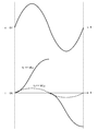
- FIG. 2 is an operation waveform diagram of the energy regeneration circuit 2 of FIG.
- FIG. 2 shows waveforms of an output voltage V OUT , a coil current i, and a displacement (corresponding to an integrated value of electromotive force) x of a vibration power generation element.
- the energy extraction circuit 20 alternately repeats the on state ⁇ ON and the off state ⁇ OFF of the switching transistor 22.
- the switching transistor 22 is turned on phi ON, the current i of the inner coil L O is gradually increased with time. Then, the timing at which the current i becomes maximum, i.e. momentarily at the maximum timing flux energy of the inner coil L O, switches to state phi OFF.
- Phase difference ⁇ of the displacement x and coil current i is determined according to r O and L O.
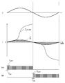
- FIG. 3 is a diagram showing a current waveform in SMFE technology.
- r O output impedance
- the power supply circuit includes a switching transistor, a rectifying element and a capacitor that form a boost converter together with an internal coil, and a controller that switches the switching transistor a plurality of times between the half waves of the AC output of the electromagnetic induction type power generation element.
- the internal resistance r O takes out electric power at a high efficiency from the power generating element of a large inductive.
- FIG. 1 It is an equivalent circuit diagram of the energy regeneration circuit using SMFE technology. It is an operation waveform diagram of the energy regeneration circuit of FIG. It is a figure which shows the current waveform in SMFE technology. It is a circuit diagram of the energy harvesting circuit which concerns on embodiment. It is operation waveform diagram of the energy harvesting circuit of FIG. It is a circuit diagram of the energy harvesting circuit which concerns on Example 1. FIG. It is operation waveform diagram of the energy harvesting circuit of FIG. It is a circuit diagram of the energy harvesting circuit which concerns on Example 2. FIG. It is operation waveform diagram of the energy harvesting circuit of FIG. It is a waveform diagram of the coil current IL and the output voltage V OUT of the energy harvesting circuit of FIG.
- FIG. 11 (a) and 11 (b) are waveform diagrams of the output voltage V OUT at the start of the energy harvesting circuit of FIG. It is a circuit diagram of the energy harvesting circuit which concerns on Example 3.
- FIG. It is a circuit diagram of the energy harvesting circuit which concerns on Example 4.
- FIG. It is a circuit diagram of the energy harvesting circuit which concerns on Example 5.
- FIG. It is a circuit diagram of the energy harvesting circuit which concerns on modification 1.
- FIG. 16 (a) to 16 (c) are circuit diagrams of the energy harvesting circuit according to the modified examples 2 to 4.
- the power supply circuit extracts electric power from an electromagnetic induction type power generation element including an internal coil and an internal resistance.
- the power supply circuit includes a switching transistor, a rectifying element and a capacitor that form a boost converter together with an internal coil, and a controller that switches the switching transistor a plurality of times between the half waves of the AC output of the electromagnetic induction type power generation element.
- the power supply circuit may further include an inductor connected in series with the internal coil.
- the electromagnetic induction type power generation element may be a magnetostrictive vibration power generation element.
- the "state in which the member A is connected to the member B" means that the member A and the member B are physically directly connected, or the member A and the member B are electrically connected to each other. It also includes the case of being indirectly connected via other members, which does not substantially affect the connection state or does not impair the functions and effects performed by the combination thereof.
- a state in which the member C is provided between the member A and the member B means that the member A and the member C, or the member B and the member C are directly connected, and their electricity. It also includes cases of being indirectly connected via other members that do not substantially affect the connection state or impair the functions and effects performed by the combination thereof.
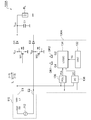
- FIG. 4 is a circuit diagram of the energy harvesting circuit 100 according to the embodiment.
- the energy harvesting circuit 100 includes an electromagnetic induction type power generation element 110 and a power supply circuit 120, and supplies electric power to the load circuit RL.
- the power generation element 110 is an electromagnetic induction type power generation element and includes an internal coil L1 and an internal resistance R1.
- the power generation element 110 is a magnetostrictive vibration power generation element including a magnetostrictive element and a coil, a power generation element including a permanent magnet and a coil, and the like.
- the equivalent circuit of the power generation element 110 is a series connection circuit of an ideal voltage source 112 that generates an electromotive force v, an internal coil L1, and an internal resistance R1.
- the internal resistance R1 has a magnitude that cannot be ignored with respect to the impedance ⁇ L1 of the coil, for example, in the range of R1> ⁇ L1 / 2. This technology is effective.
- the power supply circuit 120 takes out electric power from the electromagnetic induction type power generation element 110.
- the power supply circuit 120 includes switching transistors (switching transistors) M1 and M2, a rectifying element D1, a rectifying element D2, an output capacitor C1, and an output capacitor.
- the switching transistors M1 and M2, the rectifying elements D1 and D2, and the output capacitor C1 form a diode rectifying type boost converter 102 together with the internal coil L1.
- the controller 130 drives the switching transistors M1 and M2 at a frequency f sw (> 2f) higher than twice the frequency f (that is, the frequency of the electromotive force v) of the electromagnetic induction type power generation element 110.
- a frequency f sw > 2f
- twice the frequency f that is, the frequency of the electromotive force v
- the controller 130 drives the switching transistors M1 and M2 at a frequency f sw (> 2f) higher than twice the frequency f (that is, the frequency of the electromotive force v) of the electromagnetic induction type power generation element 110.
- a frequency f sw higher than twice the frequency f (that is, the frequency of the electromotive force v) of the electromagnetic induction type power generation element 110.
- FIG. 5 is an operation waveform diagram of the energy harvesting circuit 100 of FIG.
- the switching transistor M1 is switched, the switching transistor M2 is fixed to ON.
- the switching transistor M1 is turned on during the on time T ON determined by the time constant L / R, and is turned off during the subsequent off time T OFF .
- the off time T OFF may be shorter than the on time T ON.
- the energy stored in the coil L1 is zero, that is, may be determined coil current I L on the basis of the time tau 2 required to return to zero.
- V F is the forward voltage of the diode D1, D2.
- v, dI L / dt -V OUT / L
- the change rate of the coil current I L in accordance with the voltage V OUT of the output capacitor C1 is increased the faster.
- Coil current I L of the power generating element 110 is increased in the ON time T ON of the switching transistor M1, decrease in the off time T OFF of the switching transistor M1.
- Period T2 I L ⁇ 0 the switching transistor M2 is switched, the switching transistor M1 is fixed to ON. Like the switching transistor M2, the switching transistor M2 is turned on during the on time T ON determined by the time constant L / R, and is turned off during the subsequent off time T OFF . Envelope of the coil current I L in the period T2 also becomes possible to vary according to v / R.
- the switching frequency f SW is set higher than twice the frequency f of the power generation element 110, and the switching transistors M1 and M2 are switched at high speed, so that the internal resistance R1 is higher than the impedance ⁇ L1 of the coil.
- the switching transistors M1 and M2 are switched at high speed, so that the internal resistance R1 is higher than the impedance ⁇ L1 of the coil.
- FIG. 6 is a circuit diagram of the energy harvesting circuit 100A according to the first embodiment.
- the controller 130A includes a timing generator 132, a logic circuit 134, a polarity determination circuit 136, a zero current detection circuit 138, and drivers DR1 and DR2.
- the period T P is the sum of the on period T ON and the off period T OFF.
- the timing signal TG defines the start timing of the off period T OFF.
- Polarity determination circuit 136 determines the polarity of the coil current I L, and generates a polarity detection signal POL.
- the zero current detection circuit 138 asserts the zero current detection signal ZC when the coil current IL becomes zero.
- the logic circuit 134 generates control pulses G1 and G2 of the switching transistor M1 and the switching transistor M2 based on the timing signal TG, the polarity detection signal POL, and the zero current detection signal ZC.
- the driver DR1 drives the switching transistor M1 based on the control pulse G1
- the driver DR2 drives the switching transistor M2 based on the control pulse G2.
- Logic circuit 134 in accordance with the polarity POL of the coil current I L, selects the switching transistor to be off in the OFF period T OFF. That is , when IL > 0, the switching transistor M1 is turned off and the switching transistor M2 is turned on during the off period T OFF. On the contrary, when IL ⁇ 0, the switching transistor M2 is turned off and the switching transistor M1 is turned on during the off period T OFF.
- Logic circuit 134 is responsive to the zero current detection signal ZC, transition to on-period T ON, during the on-period T ON, the both switching transistors M1, M2 to the ON state. Then, in response to the assertion of the next timing signal TG, the process returns to the off period T OFF.
- FIG. 7 is an operation waveform diagram of the energy harvesting circuit 100A of FIG.
- the switching transistors M1, M2 is turned on, the coil current I L increases with time.
- the output capacitor C1 is discharged by the load current, so that the output voltage V OUT drops.
- the off period transitions to T OFF.
- the switching transistor M1 is turned off during the off period T OFF , the output capacitor C1 is charged by the charging current ICHG via the rectifier diode D1, and the output voltage V OUT. Rise.
- the charging current I CHG in OFF period T OFF is consistent with the coil current I L. Coil current I L, it decreases with time. When the time t 2 in the coil current I L becomes zero, the zero current detection signal ZC is asserted, a transition to the ON period T ON. During the ON period, both the switching transistors M1 and M2 are ON. Then, when the timing signal TG is asserted again at time t 3 , the off period transitions to T OFF. The energy harvesting circuit 100A repeats this operation.
- FIG. 8 is a circuit diagram of the energy harvesting circuit 100B according to the second embodiment.
- the energy harvesting circuit 100B includes a power generation element 110, switching transistors M1 and M2, transistors M3, output capacitors C1, rectifier diodes D1 and D2, drivers DR1 to DR3, and a controller 130B.
- the controller 130B includes a timing generator 132, a logic circuit 134, and a detection circuit 140.
- Detection circuit 140 also serves the function of the polarity judgment circuit 136 and the zero current detection circuit 138 of FIG. 6, for detecting the polarity of the coil current I L, the timing of the coil current I L becomes zero (current zero cross point) ..
- the controller 130B provides a polarity determination period within the switching cycle, and determines the direction (polarity) of the coil current in the polarity determination period.
- the polarity determination period is generated based on the timing signal OPEN.
- the timing signal OPEN is at a high level during the polarity determination period.
- the cycle of the timing signal OPEN is based on the operation cycle of the energy harvesting circuit 100, that is, the sum of the on-time T ON and the off time T OFF.
- the logic circuit 134 turns off both the switching transistors M1 and M2 while the OPEN signal is high.
- the coil current I L is a first polarity (I L> 0)
- the coil current I L, to flow in the body diode of the switching transistor M2 the drain voltage V D2 of the switching transistor M2 becomes negative voltage
- the switching transistor M1 A positive voltage V D1 corresponding to the countercurrent force is generated in the drain of.
- the coil current I L is the second polarity (I L ⁇ 0)
- the coil current I L to flow in the body diode of the switching transistor M1
- the drain voltage V D1 of the switching transistor M1 becomes negative voltage
- the switching transistor M2 A positive voltage V D2 corresponding to the countercurrent force is generated in the drain of.
- the detection circuit 140 detects which of the drain voltages V D1 and V D2 of the two switching transistors M1 and M2 is positive (high level).
- the detection circuit 140 includes flip-flops FF1 and FF2 and OR gates OR1 and OR2.
- the power supply terminals of the flip-flops FF1 and FF2 are connected to the first end E1 and the second end E2 of the power generation element 110.
- the set terminal of the first flip-flop FF1 is connected to the first end E1 of the power generation element 110, and its reset terminal is connected to the second end E2 of the power generation element 110.
- the set terminal of the second flip-flop FF2 is connected to the second end E2 of the power generation element 110, and the reset terminal thereof is connected to the first end E1 of the power generation element 110.
- the first OR gate OR1 generates the logical sum KEEP_INUP of the non-inverting output Q1 of the first flip-flop FF1 and the inverted output Q2B of the second flip-flop FF2.
- the second OR gate OR2 generates KEEP_INBT, which is the logical sum of the inverted output Q1B of the first flip-flop FF1 and the non-inverting output Q2 of the second flip-flop FF2.
- the logic circuit 134 includes an OR gate OR3 and a NOR gate NOR1 and NOR2.
- the first NOR gate NOR1 generates a negative OR of the output KEEP_INUP of the first OR gate OR1 and the timing signal OPEN.
- the second NOR gate NOR2 generates the negative OR of the output KEEP_INBT of the second OR gate OR2 and the timing signal OPEN.
- the third OR gate OR3 generates the OR gate OR1, OR2 output KEEP_INUP and the logical sum of KEEP_INBT.
- the driver DR3 drives the transistor M3 according to the output of the third OR gate OR3.
- FIG. 9 is an operation waveform diagram (simulation) of the energy harvesting circuit 100B of FIG.
- the open signal OPEN goes high at time t 0
- the current is flowing in the direction of IL> 0.
- V D1 rises and V D2 becomes a negative voltage.
- the flip-flop FF1 becomes operational, by high voltage V D1 to the set terminal is input at time t 1, Q1 signal goes high, KEEP_INUP signal also becomes high. If, if I L ⁇ 0, Q1B signal goes high, KEEP_INBT signal also becomes high. That output KEEP_INUP, KEEP_INBT detection circuit 140 represents the polarity of the coil current I L.
- the KEEP_INBT signal is low.
- the SWBT signal becomes high and the switching transistor M2 becomes on.
- the gate signal GATE of time t 1 to the transistor M3 becomes high.
- KEEP_INUP signal and KEEP_INBT signal indicates that the coil current I L has dropped to near zero.
- the process proceeds to the on-period T ON, the gate signal SWUP, SWBT becomes both high, the switching transistors M1, M2 is turned on.
- the ON period TON continues until the next OPEN signal transitions to high.
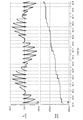
- Figure 10 is a waveform diagram of the coil current I L and the output voltage V OUT of the energy harvesting circuit 100B of FIG.
- FIG. 11 (a) and 11 (b) are waveform diagrams of the output voltage V OUT at the time of starting the energy harvesting circuit 100B of FIG.
- FIG. 11A shows a waveform when the electromotive force v of the power generation element 110 is 0.5V
- FIG. 11B shows a waveform when the electromotive force v is 0.1V.
- FIGS. 11 (a) and 11 (b) in addition to the output waveform (i) of the energy harvesting circuit 100B, the theoretical limit at the time of impedance matching (ii) and the diode when a five-stage charge pump is used (iv).
- the waveforms when the rectifier circuit is used (iv) and when the SMFE technology is used (v) are shown.
- the charging speed of 50% of the theoretical limit can be maintained, and a larger amount of electric power can be taken out as compared with other methods.
- FIG. 12 is a circuit diagram of the energy harvesting circuit 100C according to the third embodiment.
- the energy harvesting circuit 100C is obtained by omitting the transistor M3 and related elements from the energy harvesting circuit 100B of FIG.
- FIG. 13 is a circuit diagram of the energy harvesting circuit 100D according to the fourth embodiment.
- the controller 130D includes a timing generator 132, a logic circuit 134, a polarity determination circuit 136, an on-time timer 142, and drivers DR1 and DR2.
- the timing generator 132 includes an oscillator which oscillates at a duty cycle T P of energy harvesting circuit 100D, and outputs a timing signal S ON.
- the logic circuit 134 transitions to the ON period TON in response to the timing signal SON, and outputs a start trigger to the ON time timer 142.
- On-time timer 142 in response to the start trigger to start measurement of the on-time T ON, after the elapse of the on-time T ON, outputs a turn-off signal S OFF.
- the on-time TON is determined based on the time constant L / R.
- Logic circuit 134 is responsive to the turn-off signal S OFF, transitions to OFF period T OFF, in response to the next timing signal TG, transitions to the ON period T ON.
- FIG. 14 is a circuit diagram of the energy harvesting circuit 100E according to the fifth embodiment.
- the controller 130E includes a logic circuit 134, a polarity determination circuit 136, a zero current detection circuit 138, an on-time timer 142, and drivers DR1 and DR2.
- the zero current detection circuit 138 detects that the coil current IL has dropped to near zero during the off period T OFF , and generates a turn-on signal (zero current detection signal) SON.
- the logic circuit 134 transitions to the ON period TON in response to the turn-on signal SON, and outputs a start trigger to the ON time timer 142.
- On-time timer 142 in response to the start trigger to start measurement of the on-time T ON, after the elapse of the on-time T ON, outputs a turn-off signal S OFF.
- the on-time TON is determined based on the time constant L / R.
- the logic circuit 134 transitions to the off period T OFF in response to the turn-off signal S OFF.
- FIG. 15 is a circuit diagram of the energy harvesting circuit 100F according to the first modification.
- the power supply circuit 120F includes an inductor L2 provided in series with the internal coil L1.
- 16 (a) to 16 (c) are circuit diagrams of the energy harvesting circuits 100G to 100I according to the modified examples 2 to 4.
- the power supply circuit 120G of FIG. 16A is a modification of the topology of the power supply circuit 120A of FIG. 6 to a synchronous rectification type, and includes synchronous rectification transistors M3 and M4 in place of the diodes D1 and D2.
- the controller 130G includes, in the OFF period T OFF is a I L> 0, to turn on the synchronous rectification transistor M3, the OFF period T OFF is a I L ⁇ 0, to turn on the synchronous rectification transistor M4.
- the topology of the power supply circuit 120H in FIG. 16B is similar to that in FIG. In this format, the detection of the polarity of the coil current I L is not necessary.
- the topology of the power supply circuit 120I in FIG. 16C is a modification of the configuration of the power supply circuit 120H in FIG. 16B to a synchronous rectification type.
- This disclosure relates to energy harvesting.
- Boost converter 110 Power generation element 112 Voltage source R1 Internal resistance L1 Internal coil L2 Incubator 120 Power supply circuit M1, M2 Switching transistor D1, D2 Rectifier element C1, C2 Output capacitor 130 Controller 132 Timing generator 134 Logic circuit 136 Polarity Judgment circuit 138 Zero current detection circuit DR1 1st driver DR2 2nd driver
Landscapes
- Engineering & Computer Science (AREA)
- Power Engineering (AREA)
- Dc-Dc Converters (AREA)
- Rectifiers (AREA)
Abstract
電源回路120は、内部コイルL1および内部抵抗R1を含む電磁誘導型発電素子110から電力を取り出す。スイッチングトランジスタM1,M2、整流ダイオードD1,D2、出力キャパシタC1は、内部コイルL1とともに昇圧コンバータを形成する。コントローラ130は、スイッチングトランジスタM1,M2を、電磁誘導型発電素子110の周波数の2倍より高い所定の周波数で駆動する。
Description
本開示は、環境発電に関する。
光、熱、振動、風などの再生可能エネルギー(環境エネルギーともいう)を電力に変換する環境発電素子(エネルギーハーベスト素子とも称される)が注目されている。
発電素子は、大きく、直流出力のものと、交流出力のものに分けられる。発電素子が電力を供給すべき負荷回路は直流の電源を必要とするため、交流出力の発電素子を用いる場合、その出力を交流から直流に変換する必要がある。
一般に、交流を直流に変換するためには、整流回路が用いられる。発電素子の出力電圧がダイオードの順方向電圧Vfよりも十分に大きい場合、ダイオード整流回路を用いることができるが、発電素子の出力電圧がそれほど大きくない場合、同期整流回路(同期検波回路)を用いる必要がある。同期整流回路は、複数のトランジスタを含み、発電素子の交流出力と同期して、複数のトランジスタをスイッチングすることにより、交流電圧を直流電圧に変換する。
コイルの起電力を利用する電磁誘導型の発電素子と同期整流回路を組み合わせると、発電素子の大きなリアクタンスが共振回路を形成するため、発電素子の電流が非ゼロのタイミングで同期整流回路の状態を遷移させると(ハードスイッチング)、回路が発振する。
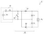
整流回路を用いずに、電磁誘導型の発電素子から直接電力を取り出す技術が提案されている(非特許文献1)。この技術は、SMFE(Synchronized Magnetic Flux Extraction)と称される。図1は、SMFE技術を用いたエネルギ再生回路2の等価回路図である。
エネルギ再生回路2は、発電素子10と、エネルギ取り出し回路20を備え、負荷Rに電力を供給する。発電素子10は、交流電圧源12、抵抗rO、インダクタンスLOの直列回路としてモデリングされる。取り出し回路20は、スイッチングトランジスタ22、整流素子D1,D2,キャパシタC1,C2を含む。
インダクタンスLOおよびエネルギ取り出し回路は、昇圧コンバータ(Boost converter)を構成している。
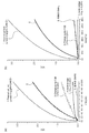
SMFE技術では、発電素子10の振動と同期して、スイッチングトランジスタ22を制御する。図2は、図1のエネルギ再生回路2の動作波形図である。図2には、出力電圧VOUT、コイル電流i、振動発電素子の変位(起電力の積分値に相当)xの波形が示される。エネルギ取り出し回路20は、スイッチングトランジスタ22がオンの状態φONと、オフの状態φOFFを交互に繰り返す。スイッチングトランジスタ22がオンの状態φONでは、内部コイルLOの電流iが時間とともに増大していく。そして、電流iが最大となるタイミング、すなわち内部コイルLOの磁束エネルギが最大のタイミングで一瞬、状態φOFFに切り替わる。この短い状態φOFFにおいて、内部コイルLOに蓄えられた磁束エネルギーが、整流素子D1を介してキャパシタC1に、またはD2を介してC2に供給され、出力電圧VOUTが上昇する。変位xとコイル電流iの位相差θは、rOとLOに応じて定まる。
E. Arroyo, A. Badel, "Electromagnetic vibration energy harvesting device optimization by synchronous energy extraction", Sensors and Actuators A 171, 266 (2011).
本発明者は、SMFE技術を、内部抵抗rO(出力インピーダンス)が数百Ω~数kΩである発電素子10に適用することを検討し、以下の課題を認識するに至った。図3は、SMFE技術における電流波形を示す図である。rO≪ωLOの領域では、インダクタンスの影響が支配的であり、電流iは、式(1)で表される。vは、電圧源12の発生電圧である。
i=∫v/LOdt …(1)
交流電圧vの半周期ごとにピークをとることとなり、SMFE技術によって、発電素子10から高効率でエネルギを取り出すことができる。
i=∫v/LOdt …(1)
交流電圧vの半周期ごとにピークをとることとなり、SMFE技術によって、発電素子10から高効率でエネルギを取り出すことができる。
しかしながら、rOがωLOに対して無視できない領域では、内部抵抗rOの影響が支配的となり、発電素子10の電流iは式(2)で表される。
i=v/rO …(2)
電流iのピークは、電圧vのピークと一致しており、このときのピーク電流は、rO≪ωLOの場合に比べて大幅に小さくなる。したがってSMFE技術では、内部抵抗rOが大きな発電素子10からは、効率よく電力を取り出すことができない。
i=v/rO …(2)
電流iのピークは、電圧vのピークと一致しており、このときのピーク電流は、rO≪ωLOの場合に比べて大幅に小さくなる。したがってSMFE技術では、内部抵抗rOが大きな発電素子10からは、効率よく電力を取り出すことができない。
本開示は係る状況においてなされたものであり、そのある態様の例示的な目的は、内部抵抗rOが大きな電磁誘導型の発電素子から高効率で電力を取り出すことが可能な電源回路の提供にある。
本開示のある態様は、内部コイルおよび内部抵抗を含む電磁誘導型発電素子から電力を取り出す電源回路に関する。電源回路は、内部コイルとともに昇圧コンバータを形成するスイッチングトランジスタ、整流素子およびキャパシタと、電磁誘導型発電素子の交流出力の半波の間に、スイッチングトランジスタを複数回、スイッチングさせるコントローラと、を備える。
なお、以上の構成要素の任意の組合せ、本発明の表現を装置、方法、システムなどの間で変換したものもまた、本発明の態様として有効である。
本開示によれば、内部抵抗rOが大きな電磁誘導型の発電素子から高効率で電力を取り出すことができる。
本開示のいくつかの例示的な実施形態の概要を説明する。この概要は、後述する詳細な説明の前置きとして、実施形態の基本的な理解を目的として、1つまたは複数の実施形態のいくつかの概念を簡略化して説明するものであり、発明あるいは開示の広さを限定するものではない。この概要は、考えられるすべての実施形態の包括的な概要ではなく、すべての実施形態の重要な要素を特定することも、一部またはすべての態様の範囲を線引きすることも意図していない。便宜上、「一実施形態」は、本明細書に開示するひとつの実施形態(実施例や変形例)または複数の実施形態(実施例や変形例)を指すものとして用いる場合がある。
一実施形態に係る電源回路は、内部コイルおよび内部抵抗を含む電磁誘導型発電素子から電力を取り出す。電源回路は、内部コイルとともに昇圧コンバータを形成するスイッチングトランジスタ、整流素子およびキャパシタと、電磁誘導型発電素子の交流出力の半波の間に、スイッチングトランジスタを複数回、スイッチングさせるコントローラと、を備える。
この構成によれば、電磁誘導型発電素子の周波数の2倍より高い周波数でスイッチングトランジスタを駆動することで、内部抵抗が大きな発電素子から高効率で電力を取り出すことができる。
一実施形態において、内部コイルのインダクタンスをL、内部抵抗をRとするとき、スイッチングトランジスタのオン期間の長さは、時定数τ=L/Rの0.3~3倍であってもよい。この場合に、インピーダンスマッチングがとれ、最大電力を取り出すことができる。
一実施形態において、電源回路は、内部コイルと直列に接続されるインダクタをさらに備えてもよい。
一実施形態において、内部コイルのインダクタンスをL1、インダクタのインダクタンスをL2、内部抵抗をRとするとき、スイッチングトランジスタのオン期間の長さは、時定数τ=(L1+L2)/Rの0.3~3倍であってもよい。この場合にインピーダンスマッチングがとれ、最大電力を取り出すことができる。
一実施形態において、電磁誘導型発電素子は、磁歪式振動発電素子であってもよい。
(実施形態)
以下、好適な実施の形態について、図面を参照しながら説明する。各図面に示される同一または同等の構成要素、部材、処理には、同一の符号を付するものとし、適宜重複した説明は省略する。また、実施の形態は、開示および発明を限定するものではなく例示であって、実施の形態に記述されるすべての特徴やその組み合わせは、必ずしも開示および発明の本質的なものであるとは限らない。
以下、好適な実施の形態について、図面を参照しながら説明する。各図面に示される同一または同等の構成要素、部材、処理には、同一の符号を付するものとし、適宜重複した説明は省略する。また、実施の形態は、開示および発明を限定するものではなく例示であって、実施の形態に記述されるすべての特徴やその組み合わせは、必ずしも開示および発明の本質的なものであるとは限らない。
本明細書において、「部材Aが、部材Bに接続された状態」とは、部材Aと部材Bが物理的に直接的に接続される場合や、部材Aと部材Bが、それらの電気的な接続状態に実質的な影響を及ぼさない、あるいはそれらの結合により奏される機能や効果を損なわせない、その他の部材を介して間接的に接続される場合も含む。
同様に、「部材Cが、部材Aと部材Bの間に設けられた状態」とは、部材Aと部材C、あるいは部材Bと部材Cが直接的に接続される場合のほか、それらの電気的な接続状態に実質的な影響を及ぼさない、あるいはそれらの結合により奏される機能や効果を損なわせない、その他の部材を介して間接的に接続される場合も含む。
図4は、実施形態に係る環境発電回路100の回路図である。環境発電回路100は、電磁誘導型発電素子110および電源回路120を備え、負荷回路RLに電力を供給する。
発電素子110は電磁誘導型の発電素子であり、内部コイルL1および内部抵抗R1を含む。たとえば発電素子110は、磁歪素子とコイルを含む磁歪式振動発電素子や、永久磁石とコイルを含む発電素子などである。発電素子110の等価回路は、起電力vを発生する理想電圧源112と、内部コイルL1、内部抵抗R1の直列接続回路である。発電素子110の周波数をf、その角周波数をω=2πfとするとき、内部抵抗R1は、コイルのインピーダンスωL1に対して無視できない大きさを有しており、たとえばR1>ωL1/2の範囲において本技術は有効である。
電源回路120は、電磁誘導型発電素子110から電力を取り出す。電源回路120は、スイッチングトランジスタ(スイッチングトランジスタ)M1,M2、整流素子D1、整流素子D2、出力キャパシタC1、出力キャパシタを含む。スイッチングトランジスタM1,M2、整流素子D1,D2、出力キャパシタC1は、内部コイルL1とともにダイオード整流型の昇圧コンバータ102を形成している。
コントローラ130は、スイッチングトランジスタM1,M2を、電磁誘導型発電素子110の周波数f(つまり起電力vの周波数)の2倍より高い周波数fsw(>2f)で駆動する。具体的には、内部コイルL1のインダクタンスをL、内部抵抗R1をRとするとき、スイッチングトランジスタM1,M2のオン期間の長さ(オン時間ともいう)TONは、時定数τ1=L/Rにもとづいて規定され、好ましくは、オン時間TONは、時定数τ1の0.3~3倍の範囲に含まれる。コントローラ130は、IL>0の区間、スイッチングトランジスタM2をオンに固定し、スイッチングトランジスタM1をスイッチングする。またコントローラ130は、IL<0の区間、スイッチングトランジスタM1をオンに固定し、スイッチングトランジスタM2をスイッチングする。
以上が環境発電回路100の構成である。続いてその動作を説明する。図5は、図4の環境発電回路100の動作波形図である。
IL>0の期間T1、スイッチングトランジスタM1がスイッチングし、スイッチングトランジスタM2がオンに固定されている。スイッチングトランジスタM1は、時定数L/Rに応じて定まるオン時間TONの間、オンとなり、それに続くオフ時間TOFFの間、オフとなる。オフ時間TOFFは、オン時間TONに比べて短くてよい。
オフ時間TOFFは、コイルL1に蓄えられたエネルギーがゼロ、つまりコイル電流ILがゼロに戻るのに要する時間τ2にもとづいて定めればよい。この時間τ2は、
dIL/dt=(v-VOUT-VF)/L
で定まる。VFはダイオードD1,D2の順方向電圧である。VOUT≫VF,vの場合、
dIL/dt=-VOUT/L
となり、出力キャパシタC1の電圧VOUTが上昇するにしたがってコイル電流ILの変化速度は速くなる。
dIL/dt=(v-VOUT-VF)/L
で定まる。VFはダイオードD1,D2の順方向電圧である。VOUT≫VF,vの場合、
dIL/dt=-VOUT/L
となり、出力キャパシタC1の電圧VOUTが上昇するにしたがってコイル電流ILの変化速度は速くなる。
トランジスタM1のターンオフのタイミングにおけるコイル電流ILは、IL≒v/Rであるから、
(v/R)/τ2=VOUT/L
を得る。したがって時間τ2は、以下の式で表される。
τ2=(L/R)・(v/VOUT)=τ1・(v/VOUT)
(v/R)/τ2=VOUT/L
を得る。したがって時間τ2は、以下の式で表される。
τ2=(L/R)・(v/VOUT)=τ1・(v/VOUT)
たとえば、L=0.1H、R=1kΩ、v=0.1V、VOUT=1Vとすると、
τ1=L/R=100μs
τ2=τ1・(v/VOUT)=0.1ms×0.1/1=10μs
となる。
τ1=L/R=100μs
τ2=τ1・(v/VOUT)=0.1ms×0.1/1=10μs
となる。
発電素子110のコイル電流ILは、スイッチングトランジスタM1のオン時間TONにおいて増大し、スイッチングトランジスタM1のオフ時間TOFFにおいて減少する。オン時間TONを、時定数τ1=L/Rと等しくすると、コイル電流ILの包絡線は、v/Rにしたがって変化することとなる。
IL<0の期間T2、スイッチングトランジスタM2がスイッチングし、スイッチングトランジスタM1がオンに固定されている。スイッチングトランジスタM2は、スイッチングトランジスタM2と同様に、時定数L/Rに応じて定まるオン時間TONの間、オンとなり、それに続くオフ時間TOFFの間、オフとなる。期間T2におけるコイル電流ILの包絡線も、v/Rにしたがって変化することとなる。
以上が環境発電回路100の動作である。環境発電回路100によれば、スイッチング周波数fSWを発電素子110の周波数fの2倍より高くして、スイッチングトランジスタM1,M2を高速にスイッチングすることで、内部抵抗R1がコイルのインピーダンスωL1に比べて無視できないほど大きい場合に、SMFE技術に比べて多くの電力を取り出すことが可能となる。
特に、スイッチングトランジスタM1,M2のオン時間TONをL/Rに近づけることにより、インピーダンス整合が成立し、最大の電力を取り出すことが可能となる。
以下、環境発電回路100の具体的な構成をいくつかの実施例にもとづいて説明する。
(実施例1)
図6は、実施例1に係る環境発電回路100Aの回路図である。コントローラ130Aは、タイミング発生器132、ロジック回路134、極性判定回路136、ゼロ電流検出回路138、ドライバDR1,DR2を備える。
図6は、実施例1に係る環境発電回路100Aの回路図である。コントローラ130Aは、タイミング発生器132、ロジック回路134、極性判定回路136、ゼロ電流検出回路138、ドライバDR1,DR2を備える。
タイミング発生器132は、所定の周波数f(=1/TP)で発振するオシレータを含み、タイミング信号TGを生成する。周期TPは、オン期間TONとオフ期間TOFFの和である。タイミング信号TGは、オフ期間TOFFの開始タイミングを規定する。
極性判定回路136は、コイル電流ILの極性を判定し、極性検出信号POLを生成する。ゼロ電流検出回路138は、コイル電流ILがゼロとなると、ゼロ電流検出信号ZCをアサートする。
ロジック回路134は、タイミング信号TG、極性検出信号POL、ゼロ電流検出信号ZCにもとづいて、スイッチングトランジスタM1およびスイッチングトランジスタM2の制御パルスG1,G2を生成する。ドライバDR1は、制御パルスG1にもとづいてスイッチングトランジスタM1を駆動し、ドライバDR2は、制御パルスG2にもとづいてスイッチングトランジスタM2を駆動する。
ロジック回路134は、コイル電流ILの極性POLに応じて、オフ期間TOFFにおいてオフすべきスイッチングトランジスタを選択する。すなわちIL>0のとき、オフ期間TOFFにおいてスイッチングトランジスタM1をオフし、スイッチングトランジスタM2をオンする。反対に、IL<0のとき、オフ期間TOFFにおいてスイッチングトランジスタM2をオフし、スイッチングトランジスタM1をオンする。
ロジック回路134は、ゼロ電流検出信号ZCに応答して、オン期間TONに遷移し、オン期間TONの間、スイッチングトランジスタM1,M2の両方をオン状態とする。そして次のタイミング信号TGのアサートに応答して、オフ期間TOFFに戻る。
図7は、図6の環境発電回路100Aの動作波形図である。時刻t1より前のオン期間TONの間、スイッチングトランジスタM1,M2がオンとなり、コイル電流ILが時間とともに増大する。オン期間TONの間、出力キャパシタC1は負荷電流によって放電されるから、出力電圧VOUTは低下する。
時刻t1にタイミング信号TGがアサートされると、オフ期間TOFFに遷移する。この例では、IL>0であるから、オフ期間TOFFの間、スイッチングトランジスタM1がオフとされ、整流ダイオードD1を介した充電電流ICHGによって、出力キャパシタC1が充電され、出力電圧VOUTが上昇する。
オフ期間TOFFにおける充電電流ICHGは、コイル電流ILと一致する。コイル電流ILは、時間とともに減少していく。時刻t2にコイル電流ILがゼロとなると、ゼロ電流検出信号ZCがアサートされ、オン期間TONに遷移する。オン期間TONでは、スイッチングトランジスタM1,M2が両方オンとなる。そして時刻t3にタイミング信号TGが再びアサートされると、オフ期間TOFFに遷移する。環境発電回路100Aはこの動作を繰り返す。
(実施例2)
図8は、実施例2に係る環境発電回路100Bの回路図である。環境発電回路100Bは、発電素子110、スイッチングトランジスタM1,M2、トランジスタM3、出力キャパシタC1、整流ダイオードD1,D2、ドライバDR1~DR3、コントローラ130Bを備える。
図8は、実施例2に係る環境発電回路100Bの回路図である。環境発電回路100Bは、発電素子110、スイッチングトランジスタM1,M2、トランジスタM3、出力キャパシタC1、整流ダイオードD1,D2、ドライバDR1~DR3、コントローラ130Bを備える。
コントローラ130Bは、タイミング発生器132、ロジック回路134および検出回路140を備える。検出回路140は、図6の極性判定回路136とゼロ電流検出回路138の機能を兼ねており、コイル電流ILの極性と、コイル電流ILがゼロになるタイミング(電流ゼロクロス点)を検出する。
この実施例では、コントローラ130Bは、スイッチング周期内に、極性判定期間を設け、極性判定期間において、コイル電流の向き(極性)を判定する。極性判定期間は、タイミング信号OPENにもとづいて生成される。タイミング信号OPENは、極性判定期間の間、ハイレベルとなる。タイミング信号OPENの周期は、環境発電回路100の動作周期、つまりオン時間TONとオフ時間TOFFの和にもとづいている。
具体的には、ロジック回路134は、OPEN信号がハイの間、スイッチングトランジスタM1、M2を両方オフとする。コイル電流ILが第1極性(IL>0)であるとき、コイル電流ILは、スイッチングトランジスタM2のボディダイオードに流れるため、スイッチングトランジスタM2のドレイン電圧VD2は負電圧となり、スイッチングトランジスタM1のドレインには、逆起電力に応じた正の電圧VD1が発生する。コイル電流ILが第2極性(IL<0)であるとき、コイル電流ILは、スイッチングトランジスタM1のボディダイオードに流れるため、スイッチングトランジスタM1のドレイン電圧VD1は負電圧となり、スイッチングトランジスタM2のドレインには、逆起電力に応じた正の電圧VD2が発生する。検出回路140は、2つのスイッチングトランジスタM1,M2のドレイン電圧VD1,VD2のうち、いずれが正(ハイレベル)となっているかを検出する。
検出回路140は、フリップフロップFF1,FF2およびORゲートOR1,OR2を含む。フリップフロップFF1,FF2それぞれの電源端子は、発電素子110の第1端E1,第2端E2と接続される。
第1フリップフロップFF1のセット端子は発電素子110の第1端E1と接続され、そのリセット端子は発電素子110の第2端E2と接続される。第2フリップフロップFF2のセット端子は発電素子110の第2端E2と接続され、そのリセット端子は発電素子110の第1端E1と接続される。
第1ORゲートOR1は、第1フリップフロップFF1の非反転出力Q1と第2フリップフロップFF2の反転出力Q2Bの論理和KEEP_INUPを生成する。第2ORゲートOR2は、第1フリップフロップFF1の反転出力Q1Bと第2フリップフロップFF2の非反転出力Q2の論理和KEEP_INBTを生成する。
ロジック回路134は、ORゲートOR3およびNORゲートNOR1,NOR2を含む。
第1NORゲートNOR1は、第1ORゲートOR1の出力KEEP_INUPと、タイミング信号OPENの否定論理和を生成する。第2NORゲートNOR2は、第2ORゲートOR2の出力KEEP_INBTとタイミング信号OPENの否定論理和を生成する。
第3ORゲートOR3は、ORゲートOR1,OR2出力KEEP_INUPとKEEP_INBTの論理和を生成する。ドライバDR3は、第3ORゲートOR3の出力に応じてトランジスタM3を駆動する。
図9は、図8の環境発電回路100Bの動作波形図(シミュレーション)である。時刻t0にオープン信号OPENがハイになると、NORゲートNOR1,NOR2の出力G1,G2、すなわちスイッチングトランジスタM1,M2のゲート信号SWUP,SWBTがローとなり、トランジスタM1,M2がオフとなる。
ここでは、IL>0の向きに電流が流れている。トランジスタM1,M2がオフとなると、VD1が上昇し、VD2が負電圧となる。VD1の上昇の結果、フリップフロップFF1が動作可能となり、セット端子にハイ電圧VD1が入力されることにより、時刻t1に、Q1信号がハイとなり、KEEP_INUP信号もハイとなる。もし、IL<0であれば、Q1B信号がハイとなり、KEEP_INBT信号もハイとなる。つまり検出回路140の出力KEEP_INUP,KEEP_INBTは、コイル電流ILの極性を表す。
時刻t1以降、KEEP_INUP信号のハイに対応して、SWUP信号はローを維持し、スイッチングトランジスタM1はオフである。
一方、フリップフロップFF2は動作しないから、KEEP_INBT信号はローである。KEEP_INBT信号のローに対応して、SWBT信号がハイとなり、スイッチングトランジスタM2はオンとなる。
また時刻t1にトランジスタM3のゲート信号GATEはハイとなる。
時刻t1以降、ダイオードD1およびトランジスタM3を介して、キャパシタC1が充電される。コイル電流ILおよび充電電流ICHGは時間とともに減少する。コイル電流ILの減少にともない、発電素子110の第1端E1の電圧VD1は低下していく。そして時刻t2に、フリップフロップFF1の出力Q1がローとなり、KEEP_INUP信号もローとなる。時刻t1~t2が、オフ期間TOFFに相当する。
つまり、KEEP_INUP信号およびKEEP_INBT信号は、コイル電流ILがゼロ付近まで低下したことを示している。
時刻t2に、オン期間TONに移行し、ゲート信号SWUP,SWBTが両方ハイとなり、スイッチングトランジスタM1,M2がオンとなる。オン期間TONは、次にOPEN信号がハイに遷移するまで持続する。
図10は、図8の環境発電回路100Bのコイル電流ILおよび出力電圧VOUTの波形図である。
図11(a)、(b)は、図8の環境発電回路100Bの起動時の出力電圧VOUTの波形図である。図11(a)は、発電素子110の起電力vが0.5Vのとき、図11(b)は、起電力vが0.1Vのときの波形を示す。
図11(a)、(b)には、環境発電回路100Bの出力波形(i)に加えて、インピーダンス整合時の理論限界(ii)、5段のチャージポンプを用いた場合(iv)、ダイオード整流回路を用いた場合(iv)、SMFE技術を用いた場合(v)の波形を示す。
このように本実施例によれば、理論限界の50%の充電速度を維持することができ、他の手法に比べてより大きな電力を取り出すことができる。
(実施例3)
図12は、実施例3に係る環境発電回路100Cの回路図である。環境発電回路100Cは、図8の環境発電回路100Bから、トランジスタM3およびそれに関連する素子を省略したものである。
図12は、実施例3に係る環境発電回路100Cの回路図である。環境発電回路100Cは、図8の環境発電回路100Bから、トランジスタM3およびそれに関連する素子を省略したものである。
(実施例4)
図13は、実施例4に係る環境発電回路100Dの回路図である。コントローラ130Dは、タイミング発生器132、ロジック回路134、極性判定回路136、オン時間タイマ142、ドライバDR1,DR2を備える。
図13は、実施例4に係る環境発電回路100Dの回路図である。コントローラ130Dは、タイミング発生器132、ロジック回路134、極性判定回路136、オン時間タイマ142、ドライバDR1,DR2を備える。
タイミング発生器132は、環境発電回路100Dの動作周期TPで発振するオシレータを含み、タイミング信号SONを出力する。
ロジック回路134は、タイミング信号SONに応答して、オン期間TONに遷移するとともに、オン時間タイマ142にスタートトリガを出力する。オン時間タイマ142は、スタートトリガに応答してオン時間TONの測定を開始し、オン時間TONの経過後に、ターンオフ信号SOFFを出力する。オン時間TONは、時定数L/Rにもとづいて定められる。ロジック回路134は、ターンオフ信号SOFFに応答して、オフ期間TOFFに遷移し、次のタイミング信号TGに応答して、オン期間TONに遷移する。
(実施例5)
図14は、実施例5に係る環境発電回路100Eの回路図である。コントローラ130Eは、ロジック回路134、極性判定回路136、ゼロ電流検出回路138、オン時間タイマ142、ドライバDR1,DR2を備える。
図14は、実施例5に係る環境発電回路100Eの回路図である。コントローラ130Eは、ロジック回路134、極性判定回路136、ゼロ電流検出回路138、オン時間タイマ142、ドライバDR1,DR2を備える。
ゼロ電流検出回路138は、オフ期間TOFFにおいて、コイル電流ILがゼロ付近まで低下したことを検出し、ターンオン信号(ゼロ電流検出信号)SONを生成する。ロジック回路134は、ターンオン信号SONに応答して、オン期間TONに遷移するとともに、オン時間タイマ142にスタートトリガを出力する。オン時間タイマ142は、スタートトリガに応答してオン時間TONの測定を開始し、オン時間TONの経過後に、ターンオフ信号SOFFを出力する。オン時間TONは、時定数L/Rにもとづいて定められる。ロジック回路134は、ターンオフ信号SOFFに応答して、オフ期間TOFFに遷移する。
以上、本発明について、実施の形態をもとに説明した。この実施の形態は例示であり、それらの各構成要素や各処理プロセスの組み合わせにいろいろな変形例が可能なこと、またそうした変形例も本発明の範囲にあることは当業者に理解されるところである。以下、こうした変形例について説明する。
(変形例1)
図15は、変形例1に係る環境発電回路100Fの回路図である。電源回路120Fは、内部コイルL1と直列に設けられたインダクタL2を備える。オン期間TONの長さは、τ=(L1+L2)/Rにもとづいて規定される。
図15は、変形例1に係る環境発電回路100Fの回路図である。電源回路120Fは、内部コイルL1と直列に設けられたインダクタL2を備える。オン期間TONの長さは、τ=(L1+L2)/Rにもとづいて規定される。
(変形例2~4)
図16(a)~(c)は、変形例2~変形例4に係る環境発電回路100G~100Iの回路図である。図16(a)の電源回路120Gは、図6の電源回路120Aのトポロジーを同期整流型に変更したものであり、ダイオードD1,D2に代えて、同期整流トランジスタM3,M4を備える。
図16(a)~(c)は、変形例2~変形例4に係る環境発電回路100G~100Iの回路図である。図16(a)の電源回路120Gは、図6の電源回路120Aのトポロジーを同期整流型に変更したものであり、ダイオードD1,D2に代えて、同期整流トランジスタM3,M4を備える。
コントローラ130Gは、IL>0であるオフ期間TOFFにおいて、同期整流トランジスタM3をオンし、IL<0であるオフ期間TOFFにおいて、同期整流トランジスタM4をオンする。
図16(b)の電源回路120Hのトポロジーは、図1のそれと同様である。この形式の場合、コイル電流ILの極性の検出は不要である。
図16(c)の電源回路120Iのトポロジーは、図16(b)の電源回路120Hの構成を同期整流型に変更したものである。
実施の形態にもとづき、具体的な用語を用いて本発明を説明したが、実施の形態は、本発明の原理、応用を示しているにすぎず、実施の形態には、請求の範囲に規定された本発明の思想を逸脱しない範囲において、多くの変形例や配置の変更が認められる。
本開示は、環境発電に関する。
100 環境発電回路
102 昇圧コンバータ
110 発電素子
112 電圧源
R1 内部抵抗
L1 内部コイル
L2 インダクタ
120 電源回路
M1,M2 スイッチングトランジスタ
D1,D2 整流素子
C1,C2 出力キャパシタ
130 コントローラ
132 タイミング発生器
134 ロジック回路
136 極性判定回路
138 ゼロ電流検出回路
DR1 第1ドライバ
DR2 第2ドライバ
102 昇圧コンバータ
110 発電素子
112 電圧源
R1 内部抵抗
L1 内部コイル
L2 インダクタ
120 電源回路
M1,M2 スイッチングトランジスタ
D1,D2 整流素子
C1,C2 出力キャパシタ
130 コントローラ
132 タイミング発生器
134 ロジック回路
136 極性判定回路
138 ゼロ電流検出回路
DR1 第1ドライバ
DR2 第2ドライバ
Claims (6)
- 内部コイルおよび内部抵抗を含む電磁誘導型発電素子から電力を取り出す電源回路であって、
前記内部コイルとともに昇圧コンバータを形成するスイッチングトランジスタ、整流素子およびキャパシタと、
前記電磁誘導型発電素子の交流出力の半波の間に、前記スイッチングトランジスタを複数回、スイッチングさせるコントローラと、
を備えることを特徴とする電源回路。 - 前記内部コイルのインダクタンスをL、前記内部抵抗をRとするとき、前記スイッチングトランジスタのオン時間は、時定数τ=L/Rの0.3~3倍であることを特徴とする請求項1に記載の電源回路。
- 前記電源回路は、前記内部コイルと直列に接続されるインダクタをさらに備えることを特徴とする請求項1に記載の電源回路。
- 前記内部コイルのインダクタンスをL1、前記インダクタのインダクタンスをL2、前記内部抵抗をRとするとき、前記スイッチングトランジスタのオン時間は、時定数τ=(L1+L2)/Rの0.3~3倍であることを特徴とする請求項3に記載の電源回路。
- 前記電源回路において、インダクタ電流を遮断したときの電圧変化の符号から前記インダクタ電流の向きを検出し、整流を行うことを特徴とする請求項1から4のいずれかに記載の電源回路。
- 前記電磁誘導型発電素子は、磁歪式振動発電素子であることを特徴とする請求項1から5のいずれかに記載の電源回路。
Applications Claiming Priority (2)
| Application Number | Priority Date | Filing Date | Title |
|---|---|---|---|
| JP2020-111945 | 2020-06-29 | ||
| JP2020111945A JP7542250B2 (ja) | 2020-06-29 | 2020-06-29 | 電磁誘導型発電素子用の電源回路 |
Publications (1)
| Publication Number | Publication Date |
|---|---|
| WO2022004533A1 true WO2022004533A1 (ja) | 2022-01-06 |
Family
ID=79316165
Family Applications (1)
| Application Number | Title | Priority Date | Filing Date |
|---|---|---|---|
| PCT/JP2021/023841 Ceased WO2022004533A1 (ja) | 2020-06-29 | 2021-06-23 | 電磁誘導型発電素子用の電源回路 |
Country Status (2)
| Country | Link |
|---|---|
| JP (1) | JP7542250B2 (ja) |
| WO (1) | WO2022004533A1 (ja) |
Citations (3)
| Publication number | Priority date | Publication date | Assignee | Title |
|---|---|---|---|---|
| JPH08237998A (ja) * | 1995-02-23 | 1996-09-13 | Isuzu Ceramics Kenkyusho:Kk | 交流発電機の電圧制御装置 |
| JP2011050226A (ja) * | 2009-08-28 | 2011-03-10 | Merstech Inc | 電力変換装置、電力変換方法、及び、プログラム |
| JP2017118764A (ja) * | 2015-12-25 | 2017-06-29 | 株式会社Lixil | 風力発電用の出力制御装置 |
-
2020
- 2020-06-29 JP JP2020111945A patent/JP7542250B2/ja active Active
-
2021
- 2021-06-23 WO PCT/JP2021/023841 patent/WO2022004533A1/ja not_active Ceased
Patent Citations (3)
| Publication number | Priority date | Publication date | Assignee | Title |
|---|---|---|---|---|
| JPH08237998A (ja) * | 1995-02-23 | 1996-09-13 | Isuzu Ceramics Kenkyusho:Kk | 交流発電機の電圧制御装置 |
| JP2011050226A (ja) * | 2009-08-28 | 2011-03-10 | Merstech Inc | 電力変換装置、電力変換方法、及び、プログラム |
| JP2017118764A (ja) * | 2015-12-25 | 2017-06-29 | 株式会社Lixil | 風力発電用の出力制御装置 |
Also Published As
| Publication number | Publication date |
|---|---|
| JP7542250B2 (ja) | 2024-08-30 |
| JP2022011064A (ja) | 2022-01-17 |
Similar Documents
| Publication | Publication Date | Title |
|---|---|---|
| CN106487225B (zh) | 开关电源装置 | |
| US9985516B2 (en) | DC/DC converter and method for zero voltage switching | |
| Yousefzadeh et al. | Sensorless optimization of dead times in DC–DC converters with synchronous rectifiers | |
| US9479073B2 (en) | Gate drive apparatus for resonant converters | |
| US8716961B2 (en) | Switched reluctance and PM brushless DC motor drive control for electric vehicle application | |
| US9294001B2 (en) | Power converter with dead-time control function | |
| US7456620B2 (en) | Determining dead times in switched-mode DC-DC converters | |
| CN102916593B (zh) | 功率转换器电路 | |
| CN106208769B (zh) | 电力转换装置 | |
| CN105450029B (zh) | 开关电源的反馈控制方法及电路 | |
| CN111726003A (zh) | 用于操作电子功率转换器的方法和电子功率转换器 | |
| Wu et al. | Interleaved phase-shift full-bridge converter with transformer winding series–parallel autoregulated (SPAR) current doubler rectifier | |
| CN115868105A (zh) | 软开关脉冲宽度调制dc-dc功率转换器 | |
| CN110022057A (zh) | 用于操作功率变换器电路的方法和功率变换器电路 | |
| Lim et al. | Energy recovery snubber circuit for a dc–dc push–pull converter | |
| US9031140B2 (en) | Method and apparatus for transmitting combined power, control and data through an isolation barrier | |
| US9214864B2 (en) | Switch mode power supply with switchable output voltage polarity | |
| CA3033814A1 (en) | Improved power supply having two quadrant converter and techniques for operation | |
| KR100978027B1 (ko) | 전력 회생 효율 증강 시스템 | |
| JP7542250B2 (ja) | 電磁誘導型発電素子用の電源回路 | |
| CN205596020U (zh) | 开关电源的反馈控制电路 | |
| CN115622407A (zh) | 具有减小的控制器电源充电损耗和减小的电磁干扰的高侧同步整流器驱动器 | |
| CN112542951A (zh) | 车辆充电器及其控制方法 | |
| TW201717532A (zh) | 單級交流至直流轉換器 | |
| KR20150077763A (ko) | 전원 공급 장치 및 그에 포함되는 게이트 드라이버 |
Legal Events
| Date | Code | Title | Description |
|---|---|---|---|
| 121 | Ep: the epo has been informed by wipo that ep was designated in this application |
Ref document number: 21833026 Country of ref document: EP Kind code of ref document: A1 |
|
| NENP | Non-entry into the national phase |
Ref country code: DE |
|
| 122 | Ep: pct application non-entry in european phase |
Ref document number: 21833026 Country of ref document: EP Kind code of ref document: A1 |