WO2022003502A1 - 化合物、発光デバイス、発光装置、電子機器、および照明装置 - Google Patents
化合物、発光デバイス、発光装置、電子機器、および照明装置 Download PDFInfo
- Publication number
- WO2022003502A1 WO2022003502A1 PCT/IB2021/055583 IB2021055583W WO2022003502A1 WO 2022003502 A1 WO2022003502 A1 WO 2022003502A1 IB 2021055583 W IB2021055583 W IB 2021055583W WO 2022003502 A1 WO2022003502 A1 WO 2022003502A1
- Authority
- WO
- WIPO (PCT)
- Prior art keywords
- light emitting
- compound
- emitting device
- carbon atoms
- layer
- Prior art date
- Legal status (The legal status is an assumption and is not a legal conclusion. Google has not performed a legal analysis and makes no representation as to the accuracy of the status listed.)
- Ceased
Links
- 0 *c1cc(*)cc(N(c2cc(*)cc(*)c2)c(c2c3c(*)c(*)c(*)c2*)c(c(*)c(*)c(*)c2*)c2c3-c(c2c3c(*)c(*)c(*)c2*)c(c(*)c(*)c(*)c2*)c2c3N(c2cc(*)cc(*)c2)c2cc(*)cc(*)c2)c1 Chemical compound *c1cc(*)cc(N(c2cc(*)cc(*)c2)c(c2c3c(*)c(*)c(*)c2*)c(c(*)c(*)c(*)c2*)c2c3-c(c2c3c(*)c(*)c(*)c2*)c(c(*)c(*)c(*)c2*)c2c3N(c2cc(*)cc(*)c2)c2cc(*)cc(*)c2)c1 0.000 description 1
Images


















Classifications
-
- C—CHEMISTRY; METALLURGY
- C09—DYES; PAINTS; POLISHES; NATURAL RESINS; ADHESIVES; COMPOSITIONS NOT OTHERWISE PROVIDED FOR; APPLICATIONS OF MATERIALS NOT OTHERWISE PROVIDED FOR
- C09K—MATERIALS FOR MISCELLANEOUS APPLICATIONS, NOT PROVIDED FOR ELSEWHERE
- C09K11/00—Luminescent materials, e.g. electroluminescent or chemiluminescent
- C09K11/06—Luminescent materials, e.g. electroluminescent or chemiluminescent containing organic luminescent materials
-
- C—CHEMISTRY; METALLURGY
- C07—ORGANIC CHEMISTRY
- C07C—ACYCLIC OR CARBOCYCLIC COMPOUNDS
- C07C211/00—Compounds containing amino groups bound to a carbon skeleton
- C07C211/43—Compounds containing amino groups bound to a carbon skeleton having amino groups bound to carbon atoms of six-membered aromatic rings of the carbon skeleton
- C07C211/57—Compounds containing amino groups bound to a carbon skeleton having amino groups bound to carbon atoms of six-membered aromatic rings of the carbon skeleton having amino groups bound to carbon atoms of six-membered aromatic rings being part of condensed ring systems of the carbon skeleton
- C07C211/61—Compounds containing amino groups bound to a carbon skeleton having amino groups bound to carbon atoms of six-membered aromatic rings of the carbon skeleton having amino groups bound to carbon atoms of six-membered aromatic rings being part of condensed ring systems of the carbon skeleton with at least one of the condensed ring systems formed by three or more rings
-
- C—CHEMISTRY; METALLURGY
- C09—DYES; PAINTS; POLISHES; NATURAL RESINS; ADHESIVES; COMPOSITIONS NOT OTHERWISE PROVIDED FOR; APPLICATIONS OF MATERIALS NOT OTHERWISE PROVIDED FOR
- C09K—MATERIALS FOR MISCELLANEOUS APPLICATIONS, NOT PROVIDED FOR ELSEWHERE
- C09K11/00—Luminescent materials, e.g. electroluminescent or chemiluminescent
- C09K11/02—Use of particular materials as binders, particle coatings or suspension media therefor
-
- H—ELECTRICITY
- H10—SEMICONDUCTOR DEVICES; ELECTRIC SOLID-STATE DEVICES NOT OTHERWISE PROVIDED FOR
- H10K—ORGANIC ELECTRIC SOLID-STATE DEVICES
- H10K50/00—Organic light-emitting devices
- H10K50/10—OLEDs or polymer light-emitting diodes [PLED]
- H10K50/11—OLEDs or polymer light-emitting diodes [PLED] characterised by the electroluminescent [EL] layers
- H10K50/12—OLEDs or polymer light-emitting diodes [PLED] characterised by the electroluminescent [EL] layers comprising dopants
-
- H—ELECTRICITY
- H10—SEMICONDUCTOR DEVICES; ELECTRIC SOLID-STATE DEVICES NOT OTHERWISE PROVIDED FOR
- H10K—ORGANIC ELECTRIC SOLID-STATE DEVICES
- H10K85/00—Organic materials used in the body or electrodes of devices covered by this subclass
- H10K85/60—Organic compounds having low molecular weight
- H10K85/615—Polycyclic condensed aromatic hydrocarbons, e.g. anthracene
-
- H—ELECTRICITY
- H10—SEMICONDUCTOR DEVICES; ELECTRIC SOLID-STATE DEVICES NOT OTHERWISE PROVIDED FOR
- H10K—ORGANIC ELECTRIC SOLID-STATE DEVICES
- H10K85/00—Organic materials used in the body or electrodes of devices covered by this subclass
- H10K85/60—Organic compounds having low molecular weight
- H10K85/615—Polycyclic condensed aromatic hydrocarbons, e.g. anthracene
- H10K85/626—Polycyclic condensed aromatic hydrocarbons, e.g. anthracene containing more than one polycyclic condensed aromatic rings, e.g. bis-anthracene
-
- H—ELECTRICITY
- H10—SEMICONDUCTOR DEVICES; ELECTRIC SOLID-STATE DEVICES NOT OTHERWISE PROVIDED FOR
- H10K—ORGANIC ELECTRIC SOLID-STATE DEVICES
- H10K85/00—Organic materials used in the body or electrodes of devices covered by this subclass
- H10K85/60—Organic compounds having low molecular weight
- H10K85/631—Amine compounds having at least two aryl rest on at least one amine-nitrogen atom, e.g. triphenylamine
- H10K85/633—Amine compounds having at least two aryl rest on at least one amine-nitrogen atom, e.g. triphenylamine comprising polycyclic condensed aromatic hydrocarbons as substituents on the nitrogen atom
-
- H—ELECTRICITY
- H10—SEMICONDUCTOR DEVICES; ELECTRIC SOLID-STATE DEVICES NOT OTHERWISE PROVIDED FOR
- H10K—ORGANIC ELECTRIC SOLID-STATE DEVICES
- H10K2101/00—Properties of the organic materials covered by group H10K85/00
- H10K2101/10—Triplet emission
-
- H—ELECTRICITY
- H10—SEMICONDUCTOR DEVICES; ELECTRIC SOLID-STATE DEVICES NOT OTHERWISE PROVIDED FOR
- H10K—ORGANIC ELECTRIC SOLID-STATE DEVICES
- H10K2101/00—Properties of the organic materials covered by group H10K85/00
- H10K2101/20—Delayed fluorescence emission
-
- H—ELECTRICITY
- H10—SEMICONDUCTOR DEVICES; ELECTRIC SOLID-STATE DEVICES NOT OTHERWISE PROVIDED FOR
- H10K—ORGANIC ELECTRIC SOLID-STATE DEVICES
- H10K2101/00—Properties of the organic materials covered by group H10K85/00
- H10K2101/27—Combination of fluorescent and phosphorescent emission
-
- H—ELECTRICITY
- H10—SEMICONDUCTOR DEVICES; ELECTRIC SOLID-STATE DEVICES NOT OTHERWISE PROVIDED FOR
- H10K—ORGANIC ELECTRIC SOLID-STATE DEVICES
- H10K2101/00—Properties of the organic materials covered by group H10K85/00
- H10K2101/90—Multiple hosts in the emissive layer
-
- H—ELECTRICITY
- H10—SEMICONDUCTOR DEVICES; ELECTRIC SOLID-STATE DEVICES NOT OTHERWISE PROVIDED FOR
- H10K—ORGANIC ELECTRIC SOLID-STATE DEVICES
- H10K50/00—Organic light-emitting devices
- H10K50/10—OLEDs or polymer light-emitting diodes [PLED]
- H10K50/11—OLEDs or polymer light-emitting diodes [PLED] characterised by the electroluminescent [EL] layers
-
- H—ELECTRICITY
- H10—SEMICONDUCTOR DEVICES; ELECTRIC SOLID-STATE DEVICES NOT OTHERWISE PROVIDED FOR
- H10K—ORGANIC ELECTRIC SOLID-STATE DEVICES
- H10K50/00—Organic light-emitting devices
- H10K50/10—OLEDs or polymer light-emitting diodes [PLED]
- H10K50/11—OLEDs or polymer light-emitting diodes [PLED] characterised by the electroluminescent [EL] layers
- H10K50/115—OLEDs or polymer light-emitting diodes [PLED] characterised by the electroluminescent [EL] layers comprising active inorganic nanostructures, e.g. luminescent quantum dots
-
- H—ELECTRICITY
- H10—SEMICONDUCTOR DEVICES; ELECTRIC SOLID-STATE DEVICES NOT OTHERWISE PROVIDED FOR
- H10K—ORGANIC ELECTRIC SOLID-STATE DEVICES
- H10K50/00—Organic light-emitting devices
- H10K50/10—OLEDs or polymer light-emitting diodes [PLED]
- H10K50/11—OLEDs or polymer light-emitting diodes [PLED] characterised by the electroluminescent [EL] layers
- H10K50/12—OLEDs or polymer light-emitting diodes [PLED] characterised by the electroluminescent [EL] layers comprising dopants
- H10K50/121—OLEDs or polymer light-emitting diodes [PLED] characterised by the electroluminescent [EL] layers comprising dopants for assisting energy transfer, e.g. sensitization
-
- H—ELECTRICITY
- H10—SEMICONDUCTOR DEVICES; ELECTRIC SOLID-STATE DEVICES NOT OTHERWISE PROVIDED FOR
- H10K—ORGANIC ELECTRIC SOLID-STATE DEVICES
- H10K85/00—Organic materials used in the body or electrodes of devices covered by this subclass
- H10K85/30—Coordination compounds
- H10K85/341—Transition metal complexes, e.g. Ru(II)polypyridine complexes
- H10K85/342—Transition metal complexes, e.g. Ru(II)polypyridine complexes comprising iridium
Definitions
- One aspect of the invention relates to compounds, light emitting devices, light emitting devices, electronic devices, and lighting devices.
- one aspect of the present invention is not limited thereto. That is, one aspect of the present invention relates to an object, a method, a manufacturing method, or a driving method. Alternatively, one aspect of the invention relates to a process, machine, manufacture, or composition (composition of matter).
- EL electroluminescence
- These light emitting devices have a structure in which an EL layer (including a light emitting substance) is sandwiched between a pair of electrodes.
- the electrons and holes injected from each electrode are recombined in the EL layer, and the light emitting substance (organic compound) contained in the EL layer is excited. It emits light when the excited state returns to the ground state.
- excited states singlet excited state (S * ) and triplet excited state (T * ). Emission from the singlet excited state is fluorescence, and emission from the triplet excited state is phosphorescence. being called.
- TADF Thermally Activated Delayed Fluorescence
- Patent Document 1 As a light emitting device using a TADF material, a method has been proposed in which the singlet excitation energy of the TADF material is transferred to the fluorescent light emitting material by combining with the fluorescent light emitting material, and the fluorescent light emitting material is efficiently emitted (Patent Document 1). reference).
- the guest material fluorescence to the host material. It is preferable to increase the concentration ratio of the luminescent substance), but if the concentration ratio of the guest material is increased, the transfer speed of energy transfer by the Dexter mechanism is improved, and as a result, the emission efficiency is lowered, which is a trade-off relationship. It has been known. Therefore, increasing the concentration ratio of the guest material cannot be said to be an effective means for improving the luminous efficiency.
- a novel compound is provided.
- the energy from the single-term excited state (S * ) of the host material (hereinafter referred to as single-term excited energy) is efficiently received, and the triple-term excitation of the host material is performed.
- a novel compound in which energy transfer from a state (T * ) (hereinafter referred to as triple-term excitation energy) is unlikely to occur (energy transfer by a Dexter mechanism can be suppressed).
- a novel compound that can be used for a light emitting device is provided. Further, in one aspect of the present invention, a novel compound that can be used for the EL layer of a light emitting device is provided. Further, a novel light emitting device having high luminous efficiency using a novel compound which is one aspect of the present invention is provided. It also provides new light emitting devices, new electronic devices, or new lighting devices.
- One aspect of the present invention is a fluorescent luminescent substance, which is a compound represented by the following general formula (G1).
- Z 1 to Z 4 independently have a structure represented by the general formula (Z-1) or the general formula (Z-2).
- X 1 and X 2 are independently alkyl groups having 3 to 10 carbon atoms, substituted or unsubstituted cycloalkyl groups having 3 to 10 carbon atoms, and 7 carbon atoms having a crosslinked structure. It represents any one of a cycloalkyl group of 10 to 10 and a trialkylsilyl group having 3 to 12 carbon atoms.
- Ar 1 and Ar 2 each independently represent an aromatic hydrocarbon group having 6 to 13 carbon atoms, and at least one of Ar 1 and Ar 2 has the same substituent as X 1.
- R 1 to R 16 are independently hydrogen, an alkyl group having 3 to 10 carbon atoms, a substituted or unsubstituted cycloalkyl group having 3 to 10 carbon atoms, a trialkylsilyl group having 3 to 12 carbon atoms, and a substituted group. Alternatively, it represents any one of an unsubstituted aryl group having 6 to 25 carbon atoms.
- Another aspect of the present invention is a compound represented by the following general formula (G2).
- X 1 and X 2 are independently alkyl groups having 3 to 10 carbon atoms, substituted or unsubstituted cycloalkyl groups having 3 to 10 carbon atoms, and 7 to 10 carbon atoms having a crosslinked structure. It represents any one of 10 cycloalkyl groups and trialkylsilyl groups having 3 to 12 carbon atoms.
- Ar 1 and Ar 2 each independently represent an aromatic hydrocarbon group having 6 to 13 carbon atoms, and at least one of Ar 1 and Ar 2 has the same substituent as X 1.
- R 1 to R 16 are independently hydrogen, an alkyl group having 3 to 10 carbon atoms, a substituted or unsubstituted cycloalkyl group having 3 to 10 carbon atoms, and a trialkylsilyl group having 3 to 12 carbon atoms. Represents any one of a substituted or unsubstituted aryl group having 6 to 25 carbon atoms.
- Another aspect of the present invention is a compound represented by the following general formula (G3).
- X 1 to X 4 are independently alkyl groups having 3 to 10 carbon atoms, substituted or unsubstituted cycloalkyl groups having 3 to 10 carbon atoms, and 7 to 10 carbon atoms having a crosslinked structure. It represents any one of 10 cycloalkyl groups and trialkylsilyl groups having 3 to 12 carbon atoms.
- R 1 to R 16 are independently hydrogen, an alkyl group having 3 to 10 carbon atoms, a substituted or unsubstituted cycloalkyl group having 3 to 10 carbon atoms, and a trialkylsilyl group having 3 to 12 carbon atoms. Represents any one of a substituted or unsubstituted aryl group having 6 to 25 carbon atoms.
- Another aspect of the present invention is a compound represented by the general formula (G4).
- X 1 and X 2 are independently alkyl groups having 3 to 10 carbon atoms, substituted or unsubstituted cycloalkyl groups having 3 to 10 carbon atoms, and 7 to 10 carbon atoms having a crosslinked structure. It represents any one of 10 cycloalkyl groups and trialkylsilyl groups having 3 to 12 carbon atoms.
- R 1 , R 3 to R 5 , R 7 to R 9 , R 11 to R 13 , R 15 to R 16 , and R 20 to R 39 are independently hydrogen and alkyl groups having 3 to 10 carbon atoms, respectively.
- Another aspect of the present invention is a compound represented by the structural formula (100) or the structural formula (101).
- the present invention is a light emitting device using the compound according to the above-mentioned aspect of the present invention.
- the present invention also includes an EL layer held between a pair of electrodes and a light emitting device formed by using a compound according to one aspect of the present invention in the light emitting layer contained in the EL layer.
- a case where the light emitting device has a layer having an organic compound in contact with the electrode is also included in the light emitting device and is included in the present invention.
- a light emitting device having a transistor, a substrate and the like is also included in the category of the invention.
- electronic devices and lighting devices having a microphone, a camera, an operation button, an external connection portion, a housing, a cover, a support base, a speaker, or the like are also included in the scope of the invention.
- one aspect of the present invention includes a light emitting device having a light emitting device, and further includes a lighting device having a light emitting device in the category. Therefore, the light emitting device in the present specification refers to an image display device or a light source (including a lighting device). Further, a module in which a connector such as FPC (Flexible Printed Circuit) or TCP (Tape Carrier Package) is attached to the light emitting device, a module in which a printed wiring board is provided at the end of TCP, or a COG (Chip On) in the light emitting device.
- the light emitting device also includes all modules in which an IC (integrated circuit) is directly mounted by the Glass) method.
- a novel compound can be provided.
- a novel compound that can be used in a light emitting device can be provided.
- a highly reliable light emitting device can be provided.
- a novel light emitting device can be provided.
- a new light emitting device, a new electronic device, or a new lighting device can be provided.
- FIG. 1A is a diagram showing the structure of a light emitting device.
- FIG. 1B is a diagram illustrating a light emitting layer.
- FIG. 2A is a conceptual diagram of energy transfer between a general guest material and a host material.
- FIG. 2B is a conceptual diagram of energy transfer between a compound (guest material) and a host material, which is one aspect of the present invention.
- FIG. 3A is a conceptual diagram of energy transfer between compounds in the light emitting layer.
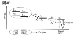
- FIG. 3B is a conceptual diagram of energy transfer between compounds in the light emitting layer.
- FIG. 3C is a conceptual diagram of energy transfer between compounds in the light emitting layer.
- FIG. 4A is a conceptual diagram of energy transfer between compounds in the light emitting layer.
- FIG. 4B is a conceptual diagram of energy transfer between compounds in the light emitting layer.
- FIG. 4C is a conceptual diagram of energy transfer between compounds in the light emitting layer.
- FIG. 5A is a conceptual diagram of energy transfer between compounds in the light emitting layer.
- FIG. 5B is a conceptual diagram of energy transfer between compounds in the light emitting layer.
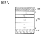
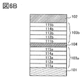
- 6A and 6B are diagrams illustrating the structure of the light emitting device.
- 7A, 7B, and 7C are diagrams illustrating a light emitting device.
- FIG. 8A is a top view illustrating the light emitting device.
- FIG. 8B is a cross-sectional view illustrating the light emitting device.
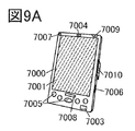
- FIG. 9A is a diagram illustrating a mobile computer.
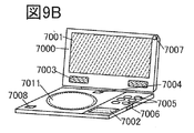
- FIG. 9B is a diagram illustrating a portable image reproduction device.
- FIG. 9C is a diagram illustrating a digital camera.
- FIG. 9D is a diagram illustrating a mobile information terminal.
- FIG. 9E is a diagram illustrating a mobile information terminal.
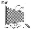
- FIG. 9F is a diagram illustrating a television device.
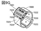
- FIG. 9G is a diagram illustrating a mobile information terminal.
- 10A, 10B, and 10C are views illustrating a foldable personal digital assistant.
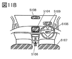
- 11A and 11B are diagrams illustrating an automobile.
- FIG. 12 is a diagram illustrating a lighting device.
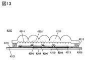
- FIG. 13 is a diagram illustrating a lighting device.
- FIG. 14 is a 1 H-NMR chart of the organic compound represented by the structural formula (100).
- FIG. 15 is an ultraviolet / visible absorption spectrum and an emission spectrum of the organic compound represented by the structural formula (100).
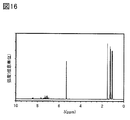
- FIG. 16 is a 1 H-NMR chart of the organic compound represented by the structural formula (101).
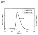
- FIG. 17 is an ultraviolet / visible absorption spectrum and an emission spectrum of the organic compound represented by the structural formula (101).
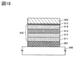
- FIG. 18 is a diagram illustrating a light emitting device.
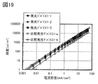
- FIG. 19 is a diagram showing the current density-luminance characteristics of the light emitting device 1-1, the light emitting device 1-2, the light emitting device 1-3, the comparative light emitting device 1-a, and the comparative light emitting device 1-b.
- FIG. 20 is a diagram showing voltage-luminance characteristics of the light emitting device 1-1, the light emitting device 1-2, the light emitting device 1-3, the comparative light emitting device 1-a, and the comparative light emitting device 1-b.
- FIG. 20 is a diagram showing voltage-luminance characteristics of the light emitting device 1-1, the light emitting device 1-2, the light emitting device 1-3, the comparative light emitting device 1-a, and the comparative light emitting device 1-b
- FIG. 21 is a diagram showing the luminance-current efficiency characteristics of the light emitting device 1-1, the light emitting device 1-2, the light emitting device 1-3, the comparative light emitting device 1-a, and the comparative light emitting device 1-b.
- FIG. 22 is a diagram showing voltage-current density characteristics of the light emitting device 1-1, the light emitting device 1-2, the light emitting device 1-3, the comparative light emitting device 1-a, and the comparative light emitting device 1-b.
- FIG. 23 is a diagram showing the brightness-power efficiency characteristics of the light emitting device 1-1, the light emitting device 1-2, the light emitting device 1-3, the comparative light emitting device 1-a, and the comparative light emitting device 1-b.
- FIG. 22 is a diagram showing voltage-current density characteristics of the light emitting device 1-1, the light emitting device 1-2, the light emitting device 1-3, the comparative light emitting device 1-a, and the comparative light emitting device 1-b.
- FIG. 23 is a diagram
- FIG. 24 is a diagram showing the luminance-external quantum efficiency characteristics of the light emitting device 1-1, the light emitting device 1-2, the light emitting device 1-3, the comparative light emitting device 1-a, and the comparative light emitting device 1-b.
- FIG. 25 is a diagram showing electroluminescence spectra of the light emitting device 1-1, the light emitting device 1-2, the light emitting device 1-3, the comparative light emitting device 1-a, and the comparative light emitting device 1-b.
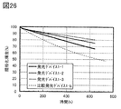
- FIG. 26 is a diagram illustrating reliability measurement results of the light emitting device 1-1, the light emitting device 1-2, the light emitting device 1-3, and the comparative light emitting device 1-b.
- FIG. 27 shows the current density-luminance characteristics of the light emitting device 2-1 and the light emitting device 2-2, the light emitting device 2-3, the light emitting device 2-4, the comparative light emitting device 2-a, and the comparative light emitting device 2-b. It is a figure.
- FIG. 28 is a diagram showing voltage-luminance characteristics of the light emitting device 2-1, the light emitting device 2-2, the light emitting device 2-3, the light emitting device 2-4, the comparative light emitting device 2-a, and the comparative light emitting device 2-b. Is.
- FIG. 28 is a diagram showing voltage-luminance characteristics of the light emitting device 2-1, the light emitting device 2-2, the light emitting device 2-3, the light emitting device 2-4, the comparative light emitting device 2-a, and the comparative light emitting device 2-b. Is.
- FIG. 28 is a diagram showing voltage-luminance characteristics of the light emitting device 2-1, the light emitting device 2-2, the light emitting device 2-3, the light emit
- FIG. 29 shows the brightness-current efficiency characteristics of the light emitting device 2-1 and the light emitting device 2-2, the light emitting device 2-3, the light emitting device 2-4, the comparative light emitting device 2-a, and the comparative light emitting device 2-b. It is a figure.
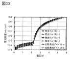
- FIG. 30 shows the voltage-current density characteristics of the light emitting device 2-1 and the light emitting device 2-2, the light emitting device 2-3, the light emitting device 2-4, the comparative light emitting device 2-a, and the comparative light emitting device 2-b. It is a figure.
- FIG. 30 shows the voltage-current density characteristics of the light emitting device 2-1 and the light emitting device 2-2, the light emitting device 2-3, the light emitting device 2-4, the comparative light emitting device 2-a, and the comparative light emitting device 2-b. It is a figure.
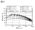
- FIG. 31 shows the brightness-power efficiency characteristics of the light emitting device 2-1 and the light emitting device 2-2, the light emitting device 2-3, the light emitting device 2-4, the comparative light emitting device 2-a, and the comparative light emitting device 2-b. It is a figure.
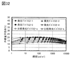
- FIG. 32 shows the brightness-external quantum efficiency characteristics of the light emitting device 2-1 and the light emitting device 2-2, the light emitting device 2-3, the light emitting device 2-4, the comparative light emitting device 2-a, and the comparative light emitting device 2-b. It is a figure which shows.
- FIG. 32 shows the brightness-external quantum efficiency characteristics of the light emitting device 2-1 and the light emitting device 2-2, the light emitting device 2-3, the light emitting device 2-4, the comparative light emitting device 2-a, and the comparative light emitting device 2-b. It is a figure which shows.
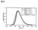
- FIG. 33 is a diagram showing electroluminescence spectra of the light emitting device 2-1, the light emitting device 2-2, the light emitting device 2-3, the light emitting device 2-4, the comparative light emitting device 2-a, and the comparative light emitting device 2-b.
- FIG. 34 is a diagram illustrating the reliability measurement results of the light emitting device 2-1 and the light emitting device 2-2, the light emitting device 2-3, the light emitting device 2-4, and the comparative light emitting device 2-b.
- the singlet excited state (S * ) is a singlet state having excitation energy.
- the S1 level is the lowest level of the singlet excited energy level, and is the excited energy level of the lowest singlet excited state (S1 state).
- the triplet excited state (T * ) is a triplet state having excitation energy.
- the T1 level is the lowest level of the triplet excited energy level, and is the excited energy level of the lowest triplet excited state (T1 state).
- it even if it is simply described as a singlet excited state and a singlet excited energy level, it may represent an S1 state and an S1 level. Further, even when the triplet excited state and the triplet excited energy level are described, they may represent the T1 state and the T1 level.
- the fluorescent light emitting substance is a compound that emits light in the visible light region or the near infrared region when relaxing from the singlet excited state to the ground state.
- the phosphorescent substance is a compound that emits light in the visible light region or the near infrared region at room temperature when relaxing from the triplet excited state to the ground state.
- the phosphorescent substance is one of the compounds capable of converting triplet excitation energy into luminescence.
- Z 1 to Z 4 independently have a structure represented by the general formula (Z-1) or the general formula (Z-2).
- X 1 and X 2 are independently alkyl groups having 3 to 10 carbon atoms, substituted or unsubstituted cycloalkyl groups having 3 to 10 carbon atoms, and 7 carbon atoms having a crosslinked structure. It represents any one of a cycloalkyl group of 10 to 10 and a trialkylsilyl group having 3 to 12 carbon atoms.
- Ar 1 and Ar 2 each independently represent an aromatic hydrocarbon group having 6 to 13 carbon atoms, and at least one of Ar 1 and Ar 2 has the same substituent as X 1.
- R 1 to R 16 are independently hydrogen, an alkyl group having 3 to 10 carbon atoms, a substituted or unsubstituted cycloalkyl group having 3 to 10 carbon atoms, a trialkylsilyl group having 3 to 12 carbon atoms, and a substituted group. Alternatively, it represents any one of an unsubstituted aryl group having 6 to 25 carbon atoms.
- Another aspect of the present invention is a compound represented by the following general formula (G2).
- X 1 and X 2 each independently have an alkyl group having 3 to 10 carbon atoms, a substituted or unsubstituted cycloalkyl group having 3 to 10 carbon atoms, and a crosslinked structure having 7 carbon atoms. It represents any one of a cycloalkyl group of 10 to 10 and a trialkylsilyl group having 3 to 12 carbon atoms.
- Ar 1 and Ar 2 each independently represent an aromatic hydrocarbon group having 6 to 13 carbon atoms, and at least one of Ar 1 and Ar 2 has the same substituent as X 1.
- R 1 to R 16 are independently hydrogen, an alkyl group having 3 to 10 carbon atoms, a substituted or unsubstituted cycloalkyl group having 3 to 10 carbon atoms, and a trialkylsilyl group having 3 to 12 carbon atoms. Represents any one of substituted or unsubstituted aryl groups having 6 to 25 carbon atoms.
- Another aspect of the present invention is a compound represented by the following general formula (G3).
- X 1 to X 4 are independently alkyl groups having 3 to 10 carbon atoms, substituted or unsubstituted cycloalkyl groups having 3 to 10 carbon atoms, and 7 carbon atoms having a crosslinked structure. It represents any one of a cycloalkyl group of 10 to 10 and a trialkylsilyl group having 3 to 12 carbon atoms.
- R 1 to R 16 are independently hydrogen, an alkyl group having 3 to 10 carbon atoms, a substituted or unsubstituted cycloalkyl group having 3 to 10 carbon atoms, and a trialkylsilyl group having 3 to 12 carbon atoms. Represents any one of a substituted or unsubstituted aryl group having 6 to 25 carbon atoms.
- Another aspect of the present invention is a compound represented by the general formula (G4).
- X 1 and X 2 each independently have an alkyl group having 3 to 10 carbon atoms, a substituted or unsubstituted cycloalkyl group having 3 to 10 carbon atoms, and a crosslinked structure having 7 carbon atoms. It represents any one of a cycloalkyl group of 10 to 10 and a trialkylsilyl group having 3 to 12 carbon atoms.
- R 1 , R 3 to R 5 , R 7 to R 9 , R 11 to R 13 , R 15 to R 16 , and R 20 to R 39 are independently hydrogen and alkyl groups having 3 to 10 carbon atoms, respectively.
- the compound according to one aspect of the present invention is a material (fluorescent light emitting substance) having a function of converting singlet excitation energy into light emission, it can be used as a guest material in the light emitting layer of a light emitting device together with a host material. ..
- a compound according to an aspect of the present invention has a chromophore that contributes to light emission and a protecting group that suppresses triplet excitation energy transfer by a Dexter mechanism from a host material to the compound.
- the luminescent group contained in the compound according to one aspect of the present invention is a condensed aromatic ring or a condensed heteroaromatic ring, and has a structure in which two or more identical skeletons are bonded.
- the protective group possessed by the compound according to one aspect of the present invention is a group having at least two aryl groups in each of the two or more diarylamino groups possessed by the compound according to one aspect of the present invention.
- a cycloalkyl group having 7 to 10 carbon atoms having a crosslinked structure an alkyl group having 3 to 10 carbon atoms, a substituted or unsubstituted cycloalkyl group having 3 to 10 carbon atoms, and a bird having 3 to 12 carbon atoms. It is one of the alkylsilyl groups.
- the transition dipole moment related to light emission becomes large, so that the molar absorption coefficient becomes large, and the host The rate of excitation energy transfer from the material by the Felster mechanism can be increased.
- the compound according to one aspect of the present invention can increase the quantum yield by having a structure in which two or more diarylamino groups having a protecting group are bonded to a luminescent group at symmetrical positions. .. Further, in the compound according to one aspect of the present invention, by using a diarylamino group, an increase in molecular weight can be suppressed and sublimation can be maintained.
- the protecting group since the protecting group has a structure that binds to the aryl group of the diarylamino group that binds to the chromophore, the protecting group can be arranged so as to cover the chromophore. The two can be separated from each other by providing a distance from the host material to the chromophore to the extent that energy transfer based on the Dexter mechanism is unlikely to occur. Further, since the effect of covering the chromophore is increased by using an aryl group having a protecting group, energy transfer based on the Dexter mechanism can be made less likely to occur.
- the aromatic hydrocarbon groups having 6 to 13 carbon atoms include phenyl group, biphenyl group, and naphthyl. Groups, fluorenyl groups and the like can be mentioned.
- alkyl group having 3 to 10 carbon atoms include, for example, a propyl group and an isopropyl group. , Butyl group, isobutyl group, sec-butyl group, tert-butyl group, pentyl group, hexyl group, heptyl group, octyl group, and the like.
- cycloalkyl group having 3 to 10 carbon atoms include, for example, a cyclopropyl group. Cyclobutyl group, cyclohexyl group, etc. may be mentioned. Specific examples of the case where the cycloalkyl group has a substituent include a methyl group, an ethyl group, a propyl group, an isopropyl group, a butyl group, an isobutyl group, a sec-butyl group, a tert-butyl group, a pentyl group and a hexyl.
- An alkyl group having 1 to 7 carbon atoms such as a group, a cyclopentyl group, a cyclohexyl group, a cycloheptyl group, a cycloalkyl group having 5 to 7 carbon atoms such as an 8,9,10-trinorbornanyl group, a phenyl group, Examples thereof include an aryl group having 6 to 12 carbon atoms such as a naphthyl group and a biphenyl group.
- cycloalkyl group having a crosslinked structure and having 7 to 10 carbon atoms include, for example, examples thereof include an adamantyl group, a bicyclo [2.2.1] heptyl group, a tricyclo [5.2.2.10 2,6 ] decanyl group, and a noradamantyl group.
- trialkylsilyl group having 3 to 12 carbon atoms include, for example, a trimethylsilyl group.
- examples thereof include a triethylsilyl group and a tert-butyldimethylsilyl group.
- an aromatic hydrocarbon group having 6 to 13 carbon atoms, a cycloalkyl group having 3 or more carbon atoms and 10 or less carbon atoms Alternatively, if any of the aryl groups having 6 to 25 carbon atoms has a substituent, the substituents include a methyl group, an ethyl group, a propyl group, an isopropyl group, a butyl group, an isobutyl group, a sec-butyl group and a tert-butyl.
- An alkyl group having 1 to 7 carbon atoms such as a group, a pentyl group and a hexyl group, and a group having 5 to 7 carbon atoms such as a cyclopentyl group, a cyclohexyl group, a cycloheptyl group and an 8,9,10-trinorbornanyl group.
- Examples thereof include a cycloalkyl group, an aryl group having 6 to 12 carbon atoms such as a phenyl group, a naphthyl group and a biphenyl group.
- aryl group having 6 to 25 carbon atoms examples include a phenyl group, a naphthyl group, and a biphenyl group. Examples thereof include a fluorenyl group and a spirofluorenyl group.
- the aryl group has a substituent, the above-mentioned alkyl group having 3 to 10 carbon atoms, the substituted or unsubstituted cycloalkyl group having 3 to 10 carbon atoms, and the trialkylsilyl group having 3 to 12 carbon atoms can be mentioned. Be done.
- Z 1 to Z 4 independently have a structure represented by the general formula (Z-1) or the general formula (Z-2).
- X 1 and X 2 are independently alkyl groups having 3 to 10 carbon atoms, substituted or unsubstituted cycloalkyl groups having 3 to 10 carbon atoms, and 7 carbon atoms having a crosslinked structure. It represents any one of a cycloalkyl group of 10 to 10 and a trialkylsilyl group having 3 to 12 carbon atoms.
- Ar 1 to Ar 2 each independently represent an aromatic hydrocarbon group having 6 to 13 carbon atoms, and at least one of Ar 1 to Ar 2 has the same substituent as X 1.
- R 1 to R 26 are independently hydrogen, an alkyl group having 3 to 10 carbon atoms, a substituted or unsubstituted cycloalkyl group having 3 to 10 carbon atoms, a trialkylsilyl group having 3 to 12 carbon atoms, and a substituted group. Alternatively, it represents any one of an unsubstituted aryl group having 6 to 25 carbon atoms.
- the compound represented by the general formula (G1) can be synthesized, for example, by the methods shown in the following synthetic scheme (S-1) and synthetic scheme (S-2).
- compound 4 (diamine compound) can be obtained by coupling compound 1, compound 2 (aniline compound), and compound 3 (aniline compound) (synthesis scheme (S-1)).
- the compound represented by the above general formula (G1) can also be synthesized by the methods shown in the following synthetic scheme (S-3), synthetic scheme (S-4), and synthetic scheme (S-5).
- compound 7 (amine compound) can be obtained by coupling compound 2 (aniline compound) and compound 5 (aryl halide) (synthesis scheme (S-3)).
- compound 8 (amine compound) can be obtained by coupling compound 3 (aniline compound) and compound 6 (aryl halide) (synthesis scheme (S-4)).
- Z 1 to Z 4 independently have a structure represented by the general formula (Z-1) or the general formula (Z-2). ..
- X 1 and X 2 are independently alkyl groups having 3 to 10 carbon atoms, substituted or unsubstituted cycloalkyl groups having 3 to 10 carbon atoms, and 7 carbon atoms having a crosslinked structure. It represents any one of a cycloalkyl group of 10 to 10 and a trialkylsilyl group having 3 to 12 carbon atoms.
- Ar 1 and Ar 2 each independently represent a substituted or unsubstituted aromatic hydrocarbon group having 6 to 13 carbon atoms, and at least one of Ar 1 and Ar 2 has the same substituent as X 1.
- R 1 to R 26 are independently hydrogen, an alkyl group having 3 to 10 carbon atoms, a substituted or unsubstituted cycloalkyl group having 3 to 10 carbon atoms, a trialkylsilyl group having 3 to 12 carbon atoms, or a trialkylsilyl group having 3 to 12 carbon atoms. Represents any one of a substituted or unsubstituted aryl group having 6 to 25 carbon atoms.
- X 10 to X 13 represent a halogen group or a triflate group, and the halogen is referred to as a halogen group. Iodine or bromine or chlorine is preferred.
- palladium compounds such as bis (dibenzilidenacetone) palladium (0) and palladium (II) acetate, tri (tert-butyl) phosphine, tri (n-hexyl) phosphine, tricyclohexylphosphine, and di (1-) Ligsins such as adamantyl) -n-butylphosphine, 2-dicyclohexylphosphine-2', 6'-dimethoxy-1,1'-biphenyl can be used.
- an organic base such as sodium tert-butoxide and an inorganic base such as potassium carbonate, cesium carbonate and sodium carbonate can be used.
- toluene, xylene, mesitylene, benzene, tetrahydrofuran, dioxane and the like can be used as the solvent, toluene, xylene, mesitylene, benzene, tetrahydrofuran, dioxane and the like.
- the reagents that can be used in the reaction are not limited to these reagents.
- the reactions carried out in the above synthetic schemes (S-1) to (S-5) are not limited to the Buchwald-Hartwig reaction, but the Ullmann-Kosugi-Still coupling reaction and Grignard reagent using an organic tin compound. Coupling reaction using the above, copper, Ullmann reaction using a copper compound, or the like can be used.
- the present invention is not limited to this, and may be synthesized by another synthetic method.
- the light emitting device comprises a first electrode 101 (in FIG. 1A, the case of an anode is shown) and a second electrode 102 (in FIG. 1A, a case of a cathode is shown).
- the EL layer 103 has a structure in which an EL layer 103 is sandwiched between a pair of electrodes, and the EL layer 103 has at least a light emitting layer 113, and also has a hole (hole) injection layer 111 and a hole (hole) transport layer 112. , An electron transport layer 114, an electron injection layer 115, and the like can be provided.
- the light emitting layer 113 has a light emitting substance (guest material) and a host material.
- guest material guest material
- the light emitting device by applying a voltage between the pair of electrodes, electrons are injected from the cathode and holes are injected from the anode into the EL layer 103, and a current flows. At this time, carriers (electrons and holes) are recombined in the light emitting layer 113 to generate excitons, and the excitation energy of the excitons is converted into light emission, so that light emission can be obtained from the light emitting device.
- carriers electros and holes
- the compound 132 which is an energy acceptor and functions as a light emitting substance (guest material) and the compound 131 which is an energy donor and functions as a host material are provided in the light emitting layer 113.
- guest material an energy acceptor and functions as a light emitting substance
- the compound 131 which is an energy donor and functions as a host material are provided in the light emitting layer 113.
- the light emitting layer 113 may have a plurality of compounds that function as host materials.
- FIG. 2A shows the configuration of a normal guest material (fluorescent light emitting substance), and shows the concept of energy transfer between the guest material and the host material when the guest material (fluorescent light emitting substance) is used.
- FIG. 2B shows the structure of compound 132, which is one aspect of the present invention, and shows the concept of energy transfer between the guest material and the host material when the compound 132 is used as the guest material.
- FIG. 2A shows the presence of compound 131, which is a host material, and fluorescent light emitting substance 124, which is a guest material.
- the fluorescent light emitting substance 124 is a general fluorescent light emitting substance, and is a fluorescent light emitting substance having a light emitting group 124a but not having a protecting group.
- FIG. 2B shows the presence of compound 131, which is a host material, and compound (fluorescent light emitting substance) 132, which is a guest material, which is one aspect of the present invention.
- Compound 132 is a fluorescent light-emitting substance that functions as an energy acceptor in a light-emitting device, and has a chromophore 132a and a protecting group 132b.
- the protecting group 132b has a function of separating the compound (host material) 131 from the compound (host material) 131 to the chromophore 132a by providing a distance such that energy transfer based on the Dexter mechanism is unlikely to occur.
- the compound 131 as the host material, the compound 124 as the guest material, and the compound (fluorescent light emitting substance) 132 are both present at close positions. Therefore, as shown in FIG. 2A, when the compound 124 does not have a protective group, the distance between the light emitting group 124a and the compound 131 becomes short, so that the energy transfer from the compound 131 to the compound 124 is performed by the Felster mechanism. Both energy transfer (Route A 6 in FIG. 2A) and energy transfer by the Dexter mechanism (Route A 7 in FIG. 2A) can occur.
- the chromophore 124a contained in the compound 124 shown in FIG. 2A and the chromophore 132a contained in the compound (fluorescent luminescent substance) 132 shown in FIG. 2B will be described.
- the chromophore (124a, 132a) refers to an atomic group (skeleton) that causes light emission in a fluorescent luminescent substance.
- the chromophores (124a, 132a) generally have a ⁇ bond and preferably contain an aromatic ring, preferably a fused aromatic ring or a condensed heteroaromatic ring.
- the transition dipole moment related to light emission becomes large, so that the molar extinction coefficient becomes large, and the excitation energy by the Felster mechanism from the host material becomes large. It is preferable because it can increase the speed of movement.
- the fused aromatic ring or condensed heteroaromatic ring contained in the chromophore (124a, 132a) include a phenanthrene ring, a stilbene ring, an acridone ring, a phenoxazine ring, and a phenothiazine ring.
- Examples thereof include a ring, a dibenzofuran ring, a dibenzothiophene ring, an indenocarbazole ring, an indolocarbazole ring, and a dibenzocarbazole ring.
- an anthracene skeleton is preferable, and it is particularly preferable to have a bianthracene skeleton in which two anthracene skeletons are bonded at the 9-position and the 10-position, respectively. ..
- the protecting group 132b of the compound (fluorescent light emitting substance) 132 shown in FIG. 2B preferably has a T1 level higher than that of the chromophore 132a and the compound 131 which is a host material.
- Specific examples of the protecting group 132b of compound 132 include an alkyl group having 3 to 10 carbon atoms, a substituted or unsubstituted cycloalkyl group having 3 to 10 carbon atoms, and 3 to 12 carbon atoms. Examples thereof include the trialkylsilyl group of.
- the light emitting layer in the light emitting device has a compound 131 that functions as a host material and a compound 132 that functions as a light emitting substance (guest material), and a TADF material is used as the compound 131 to use a light emitting material (guest material).
- the compound 132 As the compound 132, the case where a fluorescent light emitting substance is used is shown. Therefore, it is preferable to use the compound according to one aspect of the present invention as the compound 132 which is a fluorescent light emitting substance.
- An example of the correlation of the energy level in the light emitting layer 113 in this configuration example is as shown in FIG. 3A. The notation and reference numerals shown in FIG.
- 3A are as follows. Host (131): Compound 131 -Guest (132): Compound 132 ⁇ T C1: Compound 131 of T1 level ⁇ S C1: S1 levels ⁇ S G of Compound 131: S1 level ⁇ T G of Compound 132: T1 level of compound 132
- compound 131 is because it is a material having a TADF, has a function of converting the singlet excitation energy by triplet excitation energy up-conversion (route A 1 in FIG. 3A).
- the singlet excitation energy of compound 131 is rapidly transferred to compound 132. (Route A 2 in FIG. 3A).
- the relationship between S G compound 132 and S C1 of compound 131 is preferably a S C1 ⁇ S G.
- S C1 draws tangent at the short wavelength side of the hem of the fluorescence spectrum of compound 131, the energy of the wavelength of the extrapolation.
- SG is the energy of the wavelength of the absorption edge of the absorption spectrum of compound 132.
- the compound 132 is efficiently emitted (Emission). It is possible to increase the light emission efficiency of the light emitting device.
- Route A 2 compound 131 functions as an energy donor and compound 132 functions as an energy acceptor.
- the triplet excitation energy generated in the compound 131 (route A 3 in FIG. 3A) path to move T1 level of compound 132 Can also compete with.
- compound 132 is a fluorescent light-emitting substance, it is not possible to contribute triplet excitation energy into light emission, light emission efficiency of the light emitting device is reduced.
- the Felster mechanism dipole-dipole interaction
- the Dexter mechanism electrostatic interaction
- the Dexter mechanism occurs predominantly when the distance between the compound which is an energy donor and the compound which is an energy acceptor is 1 nm or less. Therefore, when the concentration of the compound which is an energy acceptor is high, the Dexter mechanism is likely to occur. Therefore, as in this configuration example, the energy acceptor compound 132 is a fluorescent material having a low triple-term excitation energy level, and when the concentration is high, the triple-term excitation energy of the energy donor compound 131 increases. and energy transfer route a 3 by Dexter mechanism, subsequent radiationless deactivation becomes dominant. Therefore, in order to suppress the route A 3, it is important to increase the distance of Compound 131 and Compound 132 to an extent hardly causes energy transfer by Dexter mechanism.
- the T1 level (TG ) of compound 132 which is an energy acceptor, is often an energy level derived from the chromophore of compound 132. Therefore, in order to suppress the route A 3 in the light-emitting layer 113, it is important to increase the distance between the luminophores compound 131 and compound 132 has.
- the concentration of the energy acceptor in the mixed film is lowered.
- the concentration of the energy acceptor is lowered, not only the energy transfer based on the Dexter mechanism from the energy donor to the energy acceptor but also the energy transfer based on the Felster mechanism is suppressed.
- the route A 2 is based on the Felster mechanism, problems such as a decrease in luminous efficiency and a decrease in reliability of the light emitting device occur.
- the compound according to one aspect of the present invention has a chromophore and a protecting group as a part of its structure, and when it functions as an energy acceptor in the light emitting layer 113, the protecting group is another energy donor. And has a function of increasing the distance from the chromophore. Therefore, when the compound according to one aspect of the present invention is used as the compound 132 having the present constitution, the distance between the compound 132 and the compound 131 can be increased. Further, when the distance between the energy donor and the energy acceptor is 1 nm or less, the Dexter mechanism becomes dominant, and when the distance is 1 nm or more and 10 nm or less, the Dexter mechanism becomes dominant.
- the protecting group is preferably a bulky substituent spreading in the range of 1 nm or more and 10 nm or less from the light emitting group, and the protecting group of the compound of one aspect of the present invention is preferably the protecting group mentioned above. Therefore, by using the compound which is one aspect of the present invention as the compound 132, it is possible to increase the energy transfer rate by the Felster mechanism while suppressing the energy transfer by the Dexter mechanism even if the concentration of the compound 132 is increased.
- the concentration of the compound 132 in the light emitting layer 113 is preferably 2 wt% or more and 50 wt% or less, more preferably 5 wt% or more and 30 wt% or less, and further preferably 5 wt% or more with respect to the compound 131 which is an energy donor. 20 wt% or less.
- the light emitting layer 113 in the light emitting device has compound 131, compound 132, and compound 133, and the compound 131 and compound 133 are a combination forming an excited complex (Exciplex), and are a light emitting substance (guest material).
- the compound 132 As the compound 132, the case where a fluorescent light emitting substance is used (when ExEF is used) is shown. Therefore, the compound according to one aspect of the present invention is preferably used as the compound 132 which is a fluorescent light emitting substance.
- FIG. 3B An example of the correlation of the energy level in the light emitting layer 113 in this configuration example is as shown in FIG. 3B.
- the notation and reference numerals shown in FIG. 3B are as follows.
- the combination of the compound 131 and the compound 133 may be any combination capable of forming an excited complex, but one is a compound having a function of transporting holes (hole transportability) and the other is a compound. It is more preferable that the compound has a function of transporting electrons (electron transportability). In this case, it becomes easy to form a donor-acceptor type excitation complex, and an excitation complex can be efficiently formed. Further, when the combination of the compound 131 and the compound 133 is a combination of a compound having a hole transport property and a compound having an electron transport property, the carrier balance can be easily controlled by the mixing ratio thereof.
- one HOMO level of compound 131 and compound 133 is higher than the other HOMO level, and one LUMO level is higher than the other LUMO level.
- the HOMO level of compound 131 may be equivalent to the HOMO level of compound 133, or the LUMO level of compound 131 may be equivalent to the LUMO level of compound 133.
- the LUMO level and HOMO level of the compound can be derived from the electrochemical properties (reduction potential and oxidation potential) of the compound measured by cyclic voltammetry (CV) measurement.
- FIG. 3B is formed by compounds 131 with compounds 133, S1 quasi-position of the exciplex (S E) and T1 level position (T E) is a energy level adjacent to each other (in FIG. 3B see route A 6).
- the excited energy levels ( SE and TE ) of the excited complex are lower than the S1 levels (SC1 and SC3 ) of each substance (Compound 131 and Compound 133) forming the excited complex, so that the excited energy is lower. It is possible to form an excited state with. As a result, the drive voltage of the light emitting device can be reduced.
- S1 quasi-position of the exciplex (S E) and the T1 level position (T E) are the energy levels adjacent to each other, they tend to reverse intersystem crossing, having TADF property. Therefore, the exciplex has a function of converting the singlet excitation energy by the up-conversion of triplet excitation energy (route A 7 in FIG. 3B). The singlet excitation energy of the excited complex can be rapidly transferred to compound 132. (Route A 8 in FIG. 3B). It preferred this time, if it is S E ⁇ S G. In Route A 8, exciplex is energy donor, compounds 132 to function as an energy acceptor.
- a tangent is drawn to the short wavelength side of the hem of the fluorescence spectrum of the exciplex, the energy of the wavelength of the extrapolation and S E, the energy of the wavelength of the absorption edge of the absorption spectrum of the compound 132 and S G when the, preferably a S E ⁇ S G.
- compounds 131 and both T1 level position of compound 133 i.e. T C1 and T C3 is preferably not less than T E.
- the emission peak wavelength on the shortest wavelength side of the phosphorescence spectra of compound 131 and compound 133 is equal to or less than the maximum emission peak wavelength of the excited complex.
- a tangent is drawn at the short wavelength side of the hem of the fluorescence spectrum of the exciplex, the energy of the wavelength of the extrapolation and S E, respectively drawing a tangent at the short wavelength side of the hem of the phosphorescence spectrum of Compound 131 and Compound 133 , the energy of the wavelength of their extrapolation line upon the T C1 and T C3 of each compound, S E -T C1 ⁇ 0.2eV and is preferably S E -T C3 ⁇ 0.2eV .
- the compound 132 can be made to emit light by transferring the triplet excitation energy generated in the light emitting layer 113 to the S1 level of the guest material compound 132 via the route A 6 and the route A 8. Therefore, by using a combination material that forms an excitation complex in the light emitting layer 113, the luminous efficiency of the fluorescent light emitting device can be improved.
- the triplet excitation energy generated in the light emitting layer 113, energy transfer route to the T1 level of the compound 132 may occur in competition. If such energy transfer (Route A 9) occurs, the fluorescent light-emitting substance, compound 132, can not be contributed triplet excitation energy into light emission, light emission efficiency of the light emitting device is lowered.
- a compound according to an aspect of the present invention has a chromophore and a protecting group as a part of its structure, and when it functions as an energy acceptor in the light emitting layer 113, the protecting group may be used with another energy donor. It has a function of increasing the distance from the chromophore. Therefore, when the compound according to one aspect of the present invention is used as the compound 132 having the present constitution, the distance between the excitation complex formed by the compound 131 and the compound 133 and the compound 132 can be increased even if the concentration of the compound 132 is increased. It can be lengthened, and the energy transfer speed by the Felster mechanism can be increased while suppressing the energy transfer by the Dexter mechanism.
- the energy transfer of the triple-term excitation energy from the excited complex to the S1 level (SG ) of the compound 132 (routes A6 and 6 in FIG. 3B). route a 8) whereas tends to occur, transfer of the triplet excitation energy from the exciplex T1 level position of compound 132 to (T G) (route a 9: can be made difficult to occur energy transfer) by the Dexter mechanism, while suppressing reduction in luminous efficiency due to energy transfer route a 9, it is possible to increase the luminous efficiency of the light emitting device. In addition, the reliability of the light emitting device can be improved.
- the routes of Route A 6 , Route A 7 , and Route A 8 described above are also referred to as ExSET (Exciplex-Singlet Energy Transfer) or ExEF (Exciplex-Enhanced Fluorescence). That is, in the light emitting layer 113 in the present specification, it is shown that the excitation energy is donated from the excitation complex to the fluorescent material.
- ExSET Exciplex-Singlet Energy Transfer
- ExEF Exciplex-Enhanced Fluorescence
- the light emitting layer 113 in the light emitting device has compound 131, compound 132, and compound 133, and the compound 131 and compound 133 are a combination forming an excited complex and function as a light emitting substance (guest material).
- a fluorescent light-emitting substance is used (when ExEF is used) is shown as the compound 132 to be used.
- the compound 133 is a phosphorescent material.
- the compound according to one aspect of the present invention is preferably used as the compound 132 which is a fluorescent light emitting substance.
- FIG. 3C An example of the correlation of the energy level in the light emitting layer 113 in this configuration example is as shown in FIG. 3C.
- the notation and reference numerals shown in FIG. 3C are the same as those in FIG. 3B, and thus the description thereof will be omitted.
- a compound having a heavy atom is used as one of the compounds forming the excitation complex. Therefore, intersystem crossing between the singlet state and the triplet state is promoted. Therefore, it is possible to form an excited complex capable of transitioning from a triplet excited state to a singlet ground state (that is, capable of exhibiting phosphorescence).
- the triplet excited energy level of the exciplex (T E) is the energy level of the donor
- singlet excitation energy level of the compound 132 T E is a light-emitting material ( SG ) or higher is preferable.
- a tangent is drawn to the short wavelength side of the skirt of the emission spectrum of the exciplex with heavy atoms, the energy of the wavelength of the extrapolation and T E, the wavelength of the absorption edge of the absorption spectrum of the compound 132 energy upon S G, it is preferable that T E ⁇ S G.
- a triplet excitation energy of the generated exciplex, singlet excitation energy level (S G compound 132 from the triplet excited energy level of the exciplex (T E) ) Can transfer energy.
- S1 quasi-position of the exciplex (S E) and the T1 level position (T E) are the energy levels adjacent to each other, in an emission spectrum, when it is difficult to clearly distinguish between fluorescence and phosphorescence There is. In that case, it may be possible to distinguish between fluorescence and phosphorescence depending on the emission lifetime.
- the phosphorescent material used in the above configuration preferably contains heavy atoms such as Ir, Pt, Os, Ru, and Pd.
- the quantum yield may be high or low. That is, the energy transfer from the triplet excited energy level of the excited complex to the singlet excited energy level of the guest material may be an allowable transition.
- the energy transfer from the excitation complex composed of the phosphorescent material or the phosphorescent material to the guest material as described above is the single-term excitation energy level of the guest material (energy acceptor) from the triple-term excitation energy level of the energy donor. This is a preferable configuration because the energy transfer to is an allowable transition.
- the triplet excitation energy of the exciplex without going through the route of the route A 7 paths (in FIG. 3C route A 8 ) to the mobile S1 level position of the guest material to (S G). That is, it is possible via the route of the route A 6 and Route A 8, moves the S1 triplet excitation energy and the singlet excitation energy to the level of the guest material.
- exciplex is the energy donor, compound 132 serves as an energy acceptor.
- the triplet excitation energy of the exciplex (route A 9 in FIG. 3C) path to move T1 level of the compound 132 also conflicts Can be.
- compound 132 is a fluorescent light-emitting substance, it is not possible to contribute triplet excitation energy into light emission, light emission efficiency of the light emitting device is reduced.
- a compound according to an aspect of the present invention has a chromophore and a protecting group as a part of its structure, and when it functions as an energy acceptor in the light emitting layer 113, the protecting group may be used with another energy donor. It has a function of increasing the distance from the chromophore. Therefore, when the compound according to one aspect of the present invention is used as the compound 132 having the present constitution, the distance between the excitation complex formed by the compound 131 and the compound 133 and the compound 132 can be increased even if the concentration of the compound 132 is increased. It can be lengthened, and the energy transfer speed by the Felster mechanism can be increased while suppressing the energy transfer by the Dexter mechanism.
- the energy transfer of the triple-term excitation energy from the excited complex to the S1 level (SG ) of the compound 132 (route A 6 and route A 8 ). while tends to occur, transfer of the triplet excitation energy from the exciplex to the T1 level (T G) position of the compound 132: can be less likely to occur (the route a 9 energy transfer by Dexter mechanism), the route a 9 It is possible to increase the light emission efficiency of the light emitting device while suppressing the decrease in light emission efficiency due to energy transfer. In addition, the reliability of the light emitting device can be improved.
- the light emitting layer 113 in the light emitting device has three kinds of substances, that is, compound 131, compound 132, and compound 133.
- compound 131 and compound 133 are combinations forming an excitation complex, and the case where a fluorescent light emitting substance is used (when ExEF is used) as compound 132 which functions as a light emitting substance (guest material) is shown. Therefore, the compound according to one aspect of the present invention is preferably used as the compound 132 which is a fluorescent light emitting substance.
- This configuration example is different from the above configuration example 3 in that compound 133 is a material having TADF properties.
- FIG. 4A An example of the correlation of the energy level in the light emitting layer 113 in this configuration example is as shown in FIG. 4A. Since the notation and reference numeral shown in FIG. 4A are common to those in FIG. 3B, the description thereof will be omitted.
- compound 133 is a TADF material
- compound 133 that does not form an excitation complex has a function of converting triplet excitation energy into singlet excitation energy by up-conversion (route A in FIG. 4A). 10 ). Therefore, the singlet excitation energy of compound 133 is rapidly transferred to compound 132. (Route A 11 in FIG. 4A). It preferred this time, if it is S C3 ⁇ S G.
- triplet excitation energy into compound 132 is a guest material a path moving, there is a path to move through the root a 10 and route a 11 in FIG. 4A to compound 132.
- the luminous efficiency can be further enhanced by the existence of a plurality of paths for the triplet excitation energy to move to the compound 132, which is a fluorescent luminescent substance.
- exciplex is energy donor, compounds 132 to function as an energy acceptor.
- compound 133 is the energy donor, compounds 132 to function as an energy acceptor.
- the triplet excitation energy of the excited complex also competes with the path (route A 9 in FIG. 4A) to move to the T1 level of the compound 132. Can be.
- route A 9 in FIG. 4A the triplet excitation energy of the excited complex
- compound 132 is a fluorescent light-emitting substance, it is not possible to contribute triplet excitation energy into light emission, light emission efficiency of the light emitting device is reduced.
- a compound according to an aspect of the present invention has a chromophore and a protecting group as a part of its structure, and when it functions as an energy acceptor in the light emitting layer 113, the protecting group may be used with another energy donor. It has a function of increasing the distance from the chromophore. Therefore, when the compound according to one aspect of the present invention is used as the compound 132 having the present constitution, the distance between the excitation complex formed by the compound 131 and the compound 133 and the compound 132 can be increased even if the concentration of the compound 132 is increased. It can be lengthened, and the energy transfer speed by the Felster mechanism can be increased while suppressing the energy transfer by the Dexter mechanism.
- the energy transfer of the triple-term excitation energy from the excited complex to the S1 level (SG ) of the compound 132 (route A 6 and route A 8 ). And the transfer of triplet excitation energy from the excited complex to the S1 level ( SG ) of compound 132 (Route A 10 and Route A 11 ) is more likely to occur, while the T1 level of compound 132 from the excited complex (Route A 10 and Route A 11) is more likely to occur.
- the light emitting layer 113 in the light emitting device has four kinds of substances, that is, compound 131, compound 132, compound 133, and compound 134.
- the compound 133 has a function of converting triplet excitation energy into light emission, and is particularly a phosphorescent light emitting substance.
- the compound 131 and the compound 134 are a combination forming an excitation complex, and a case where a fluorescent luminescent substance is used as the compound 132 that functions as a luminescent substance (guest material) is shown. Therefore, the compound according to one aspect of the present invention is preferably used as the compound 132 which is a fluorescent light emitting substance.
- FIG. 4B An example of the correlation of the energy level in the light emitting layer 113 in this configuration example is as shown in FIG. 4B.
- the notation and reference numeral in FIG. 4B are the same as those shown in FIG. 3B, and other than that, they are as shown below.
- compound 131 and compound 134 form an excited complex.
- S1 quasi-position of the exciplex (S E) and the T1 level position of the exciplex (T E) is a energy level adjacent to each other (see route A 12 in FIG. 4B).
- the excitation complex generated by the two kinds of substances in the above path loses the excitation energy, the two kinds of substances exist as the original separate substances.
- the excited energy levels ( SE and TE ) of the excited complex are lower than the S1 levels (SC1 and SC4 ) of each substance (Compound 131 and Compound 134) forming the excited complex, so that the excited energy is lower. It is possible to form an excited state with. As a result, the drive voltage of the light emitting device can be reduced.
- compound 133 is a phosphorescent material, intersystem crossing between the singlet state and the triplet state is allowed. Therefore, both the singlet and triplet excitation energies rapidly move from the excitation complex to compound 133 (Route A 13 ). It preferred this time, if it is T E ⁇ T C3.
- the triplet excitation energy of the compound 133 is converted into the singlet excitation energy of the compound 132 (Route A 14 ).
- the energy transfer takes place efficiently from the compound 133 to compound 132. More specifically, drawing a tangential line at the short wavelength side of the hem of the phosphorescence spectrum of compound 133, the energy of the wavelength of the extrapolation and T C3, the energy of the wavelength of the absorption edge of the absorption spectrum of the compound 132 S G upon a preferably a T C3 ⁇ S G.
- compound 133 functions as an energy donor and compound 132 functions as an energy acceptor.
- the combination of the compound 131 and the compound 134 may be any combination capable of forming an excited complex, but one is a compound having a hole transporting property and the other is a compound having an electron transporting property. Is more preferable.
- one HOMO level of compound 131 and compound 134 is higher than the other HOMO level, and one LUMO level is higher than the other LUMO level. Is preferable.
- the correlation of energy levels between compound 131 and compound 134 is not limited to FIG. 4B. That is, the singlet excitation energy level ( SC1 ) of compound 131 may be higher or lower than the singlet excitation energy level ( SC4) of compound 134. Further, the triplet excitation energy level ( TC1 ) of compound 131 may be higher or lower than the triplet excitation energy level ( TC4) of compound 134.
- the compound 131 has a ⁇ -electron deficient skeleton. With this configuration, the LUMO level of compound 131 is lowered, which is suitable for forming an excited complex.
- the compound 131 has a ⁇ -electron excess skeleton. With this configuration, the HOMO level of compound 131 becomes high, which is suitable for forming an excited complex.
- a compound according to an aspect of the present invention has a chromophore and a protecting group as a part of its structure, and when it functions as an energy acceptor in the light emitting layer 113, the protecting group may be used with another energy donor. It has a function of increasing the distance from the chromophore. Therefore, when the compound according to one aspect of the present invention is used as the compound 132 having the present constitution, the distance between the compound 133 and the compound 132 can be increased. Therefore, by using the compound which is one aspect of the present invention as the compound 132, the energy transfer of the triple-term excitation energy (route A 14 ) from the compound 133 to the S1 level (SG ) of the compound 132 is likely to occur.
- the transfer of triplet excitation energy from compound 133 to the T1 level ( TG ) of compound 132 can be made less likely to occur, and is accompanied by the energy transfer of route A 15. It is possible to increase the light emitting efficiency of the light emitting device while suppressing the decrease in the light emitting efficiency.
- the concentration of the compound 132 in the light emitting layer 113 is preferably 2 wt% or more and 50 wt% or less, more preferably 5 wt% or more and 30 wt% or less, and further preferably 5 wt% or more with respect to the compound 133 which is an energy donor. 20 wt% or less.
- the routes of Route A 12 and Route A 13 described above are also referred to as ExTET (Excimerx-Triplet Energy Transfer). That is, in the light emitting layer 113 in the present specification, it is shown that the excitation energy is donated from the excitation complex to the compound 133.
- ExTET Extra Transmitter-Triplet Energy Transfer
- the light emitting layer 113 in the light emitting device has four kinds of substances, that is, compound 131, compound 132, compound 133, and compound 134.
- the compound 133 has a function of converting triplet excitation energy into light emission, and is particularly a phosphorescent light emitting substance.
- the compound 131 and the compound 134 are a combination forming an excitation complex, and a case where a fluorescent luminescent substance is used as the compound 132 that functions as a luminescent substance (guest material) is shown. Therefore, the compound according to one aspect of the present invention is preferably used as the compound 132 which is a fluorescent light emitting substance.
- This configuration example is different from the above configuration example 5 in that compound 134 is a material having TADF properties. Further, an example of the correlation of the energy level in the light emitting layer 113 in this configuration example is as shown in FIG. 4C. Since the notation and reference numeral shown in FIG. 4C are common to those in FIGS. 3B and 4B, the description thereof will be omitted.
- compound 134 is a TADF material
- compound 134 which does not form an excitation complex has a function of converting triplet excitation energy into singlet excitation energy by up-conversion (route A 16 in FIG. 4C). .. Therefore, the singlet excitation energy possessed by the compound 134 is rapidly transferred to the compound 132. (Route A 17 in FIG. 4C). It preferred this time, if it is S C4 ⁇ S G.
- the triplet excitation energy is the guest material via the root A 12 , the root A 13 , and the root A 14 in FIG. 4C, similarly to the above configuration example 5.
- the luminous efficiency can be further enhanced by the existence of a plurality of paths for the triplet excitation energy to move to the compound 132, which is a fluorescent luminescent substance.
- Route A 14 compound 133 functions as an energy donor and compound 132 functions as an energy acceptor.
- compound 134 functions as an energy donor and compound 132 functions as an energy acceptor.
- the triplet excitation energy of the compound 133 with the path to move T1 level of the compound 132 (Route A 15 in FIG. 4C) competition Can be.
- the compound 132 which is a fluorescent light emitting substance, cannot contribute the triplet excitation energy to light emission, so that the luminous efficiency of the light emitting device is lowered.
- the distance between the compound 133 and the compound 132 that is, the distance between the compound 133 and the chromophore of the compound 132 is long. Is important.
- a compound according to an aspect of the present invention has a chromophore and a protecting group as a part of its structure, and when it functions as an energy acceptor in the light emitting layer 113, the protecting group may be used with another energy donor. It has a function of increasing the distance from the chromophore. Therefore, when the compound according to one aspect of the present invention is used as the compound 132 having the present constitution, the distance between the compound 133 and the compound 132 can be increased even if the concentration of the compound 132 is increased, and the energy by the Dexter mechanism can be increased. It is possible to increase the energy transfer speed by the Felster mechanism while suppressing the movement.
- the energy transfer of the triple-term excitation energy from the excited complex to the S1 level (SG ) of the compound 132 (route A 12 and route A 13 and). Both root A 14 ) and the transfer of triplet excitation energy from the excited complex to the S1 level ( SG ) of compound 132 (root A 16 and root A 17 ) are more likely to occur, while compound 133 to compound 132 It is possible to make the transfer of triplet excitation energy to the T1 level ( TG ) less likely to occur (Route A 15 : energy transfer by the Dexter mechanism), and while suppressing the decrease in emission efficiency due to the energy transfer of Route A 15. , The light emitting efficiency of the light emitting device can be increased. In addition, the reliability of the light emitting device can be improved.
- the light emitting layer 113 in the light emitting device has compound 131, compound 132, and compound 133.
- the compound 133 has a function of converting triplet excitation energy into light emission, and is particularly a phosphorescent light emitting substance.
- a case where a fluorescent luminescent substance is used as the compound 132 that functions as a luminescent substance (guest material) will be shown. Therefore, the compound according to one aspect of the present invention is preferably used as the compound 132 which is a fluorescent light emitting substance.
- An example of the correlation of the energy level in the light emitting layer 113 in this configuration example is as shown in FIG. 5A.
- singlet excitons and triplet excitons are generated mainly by carrier recombination in compound 131.
- the movement as compound 133 by selecting a phosphorescent material having the relationship of T C3 ⁇ T C1, both the singlet excitation energy and the triplet excitation energy generated in the compound 131 to T C3 level of the compound 133 (Fig. 5A Route A 18 ). It should be noted that some carriers can also be recombined with compound 133.
- the phosphorescent substance used in the above configuration preferably contains heavy atoms such as Ir, Pt, Os, Ru, and Pd.
- the energy transfer from the triplet excitation energy level of the energy donor to the singlet excitation energy level of the guest material (energy acceptor) is preferable because it is an allowable transition. Therefore, it is possible to move the triplet excitation energy of the compound 133 by the route of the route A 19 S1 level position of the guest material to the (S G).
- Route A 19 compound 133 functions as an energy donor and compound 132 functions as an energy acceptor.
- the excitation energy of the compound 133 is moved to the singlet excited state of the compound 132 which is effectively a guest material. Specifically, a tangent is drawn to the short wavelength side of the hem of the phosphorescence spectrum of compound 133, the energy of the wavelength of the extrapolation and T C3, the energy of the wavelength of the absorption edge of the absorption spectrum of the compound 132 and S G when the, preferably a T C3 ⁇ S G.
- the triplet excitation energy of compound 133 also competes with the path (route A 20 in FIG.
- a compound according to an aspect of the present invention has a chromophore and a protecting group as a part of its structure, and when it functions as an energy acceptor in the light emitting layer 113, the protecting group may be used with another energy donor. It has a function of increasing the distance from the chromophore. Therefore, when the compound according to one aspect of the present invention is used as the compound 132 having the present constitution, the distance between the compound 133 and the compound 132 can be increased even if the concentration of the compound 132 is increased, and the Dexter mechanism is used. It is possible to increase the energy transfer speed by the Felster mechanism while suppressing the energy transfer.
- the energy transfer of the triple-term excitation energy (route A 19 ) from the compound 133 to the S1 level (SG ) of the compound 132 is likely to occur.
- the transfer of triplet excitation energy from compound 133 to the T1 level ( TG ) of compound 132 can be made less likely to occur, and is accompanied by the energy transfer of route A 20. It is possible to increase the light emitting efficiency of the light emitting device while suppressing the decrease in the light emitting efficiency. In addition, the reliability of the light emitting device can be improved.
- the light emitting layer 113 in the light emitting device has compound 131, compound 132, and compound 133.
- the compound 133 has a function of converting triplet excitation energy into light emission, and is particularly a material having TADF properties. Further, a case where a fluorescent luminescent substance is used as the compound 132 that functions as a luminescent substance (guest material) will be shown. Therefore, the compound according to one aspect of the present invention is preferably used as the compound 132 which is a fluorescent light emitting substance.
- An example of the correlation of the energy level in the light emitting layer 113 in this configuration example is as shown in FIG. 5B.
- the notation and reference numeral in FIG. 5B are the same as those shown in FIG. 5A, and other than that, they are as shown below.
- SC3 S1 level of compound 133
- singlet excitons and triplet excitons are generated mainly by carrier recombination in compound 131.
- S C3 ⁇ S C1 and by selecting a material having a TADF of having a relationship T C3 ⁇ T C1, both the compound of singlet excitation energy and the triplet excitation energy generated in the compound 131 It is possible to move to the SC3 and TC3 levels of 133 (Fig. 5B Route A 21 ). It should be noted that some carriers can also be recombined with compound 133.
- compound 133 Since compound 133 is a material having TADF properties, it has a function of converting triplet excitation energy into singlet excitation energy by up-conversion (FIG. 5B Route A 22 ). Further, the singlet excitation energy of compound 133 can be rapidly transferred to compound 132. (Fig. 5B Route A 23 ). It preferred this time, if it is S C3 ⁇ S G. More specifically, drawing a tangential line at the short wavelength side of the hem of the fluorescence spectrum of compound 133, the energy of the wavelength of the extrapolation and S C3, the energy of the wavelength of the absorption edge of the absorption spectrum of the compound 132 S G upon a, it is preferable that S C3 ⁇ S G.
- the triplet excitation energy generated by the compound 133 is transferred to the compound 132 by passing through the routes of the route A 21, the route A 22 and the route A 23 in FIG. 5B. Can be converted to fluorescent light emission.
- Route A 23 compound 133 functions as an energy donor and compound 132 functions as an energy acceptor.
- the triplet excitation energy of compound 133 also competes with the path (route A 24 in FIG. 5B) to move to the T1 level of compound 132. Can be.
- the compound 132 which is a fluorescent light emitting substance, cannot contribute the triplet excitation energy to light emission, so that the luminous efficiency of the light emitting device is lowered.
- the distance between the compound 133 and the compound 132 that is, the distance between the compound 133 and the chromophore of the compound 132 is long. Is important.
- a compound according to an aspect of the present invention has a chromophore and a protecting group as a part of its structure, and when it functions as an energy acceptor in the light emitting layer 113, the protecting group may be used with another energy donor. It has a function of increasing the distance from the chromophore. Therefore, when the compound according to one aspect of the present invention is used as the compound 132 having the present constitution, the distance between the compound 133 and the compound 132 can be increased even if the concentration of the compound 132 is increased, and the energy by the Dexter mechanism can be increased. It is possible to increase the energy transfer speed by the Felster mechanism while suppressing the movement.
- the energy transfer of the triple-term excitation energy (route A 23 ) from the compound 133 to the S1 level (SG ) of the compound 132 is likely to occur.
- the energy transfer of route A 24 can be performed. It is possible to increase the light emitting efficiency of the light emitting device while suppressing the accompanying decrease in light emitting efficiency. In addition, the reliability of the light emitting device can be improved.
- FIG. 6A shows an example of a light emitting device having an EL layer including a light emitting layer between a pair of electrodes. Specifically, it has a structure in which the EL layer 103 is sandwiched between the first electrode 101 and the second electrode 102.
- the EL layer 103 has, for example, a hole injection layer 111, a hole transport layer 112, a light emitting layer 113, an electron transport layer 114, and an electron injection layer when the first electrode 101 is used as an anode.
- 115 has a structure in which the functional layers are sequentially laminated.
- the light emitting layer 113 has a host material and a guest material, uses a third organic compound as the host material, and has a function of converting singlet excitation energy into light emission as the guest material (fluorescent light emitting material). ), And a second organic compound which is a material (phosphorescent luminescent material or TADF material) having a function of converting triplet excitation energy into light emission is used.
- a light emitting device capable of low voltage drive by having a configuration (tandem structure) having a plurality of EL layers formed by sandwiching a charge generation layer between a pair of electrodes, and a light emitting device.
- a light emitting device or the like whose optical characteristics are improved by forming a micro-optical resonator (microcavity) structure between a pair of electrodes is also included in one aspect of the present invention.
- the charge generation layer has a function of injecting electrons into one of the adjacent EL layers and injecting holes into the other EL layer when a voltage is applied to the first electrode 101 and the second electrode 102. Have.
- At least one of the first electrode 101 and the second electrode 102 of the light emitting device is a translucent electrode (transparent electrode, semi-transmissive / semi-reflective electrode, etc.).
- the electrode having translucency is a transparent electrode
- the transmittance of visible light of the transparent electrode is 40% or more.
- the reflectance of visible light of the semi-transmissive / semi-reflective electrode is 20% or more and 80% or less, preferably 40% or more and 70% or less.
- the resistivity of these electrodes is 1 ⁇ 10 ⁇ 2 ⁇ cm or less.
- the reflective electrode when one of the first electrode 101 and the second electrode 102 is a reflective electrode (reflecting electrode), the reflective electrode is visible.
- the reflectance of light is 40% or more and 100% or less, preferably 70% or more and 100% or less. Further, it is preferable that the resistivity of this electrode is 1 ⁇ 10 ⁇ 2 ⁇ cm or less.
- the following materials can be appropriately combined and used as long as the functions of both electrodes described above can be satisfied.
- metals, alloys, electrically conductive compounds, and mixtures thereof can be appropriately used. Specific examples thereof include In—Sn oxide (also referred to as ITO), In—Si—Sn oxide (also referred to as ITSO), In—Zn oxide, and In—W—Zn oxide.
- Other elements belonging to Group 1 or Group 2 of the Periodic Table of Elements eg, Lithium (Li), Cesium (Cs), Calcium (Ca), Strontium (Sr)), Europium (Eu), Ytterbium Rare earth metals such as (Yb), alloys containing these in appropriate combinations, and other graphenes can be used.
- a sputtering method or a vacuum vapor deposition method can be used to prepare these electrodes.
- the hole injection layer 111 is a layer for injecting holes (holes) from the first electrode 101, which is an anode, into the EL layer 103, and is a layer containing an organic acceptor material and a material having high hole injectability.
- the organic acceptor material is a material capable of generating holes in the organic compound by separating charges between the LUMO level value and another organic compound having a similar HOMO level value. be. Therefore, as the organic acceptor material, a compound having an electron-withdrawing group (halogen group or cyano group) such as a quinodimethane derivative, a chloranil derivative, or a hexaazatriphenylene derivative can be used.
- halogen group or cyano group such as a quinodimethane derivative, a chloranil derivative, or a hexaazatriphenylene derivative
- HAT-CN 3,6- difluoro -2,5,7,7,8, 8-Hexacyanoquinodimethane
- Chloranil 2,3,6,7,10,11-Hexacyano-1,4,5,8,9,12-Hexaazatriphenylene
- F6-TCNNQ 1,3 4,5,7,8-hexafluorotetracyano-naphthoquinodimethane
- HAT-CN 3,6- difluoro -2,5,7,7,8, 8-Hexacyanoquinodimethane
- Chloranil 2,3,6,7,10,11-Hexacyano-1,4,5,8,9,12-Hexaazatriphenylene
- F6-TCNNQ 1,3 4,5,7,8-hexafluorotetracyano-naphthoquinodimethane
- F6-TCNNQ 1,3 4,5,7,8-hexafluorotetracyano-naphthoquinodimethane
- [3] radialene derivatives are preferable because they have extremely high electron acceptability, and specifically, ⁇ , ⁇ ', ⁇ ''-1,2,3-cyclopropanetriylidentry [4-cyano-].
- 2,3,5,6-Tetrafluorobenzene acetonitrile] ⁇ , ⁇ ', ⁇ ''-1,2,3-cyclopropanetriylidentris [2,6-dichloro-3,5-difluoro-4- (2,6-dichloro-3,5-difluoro-4- (2,6-dichloro-3,5-difluoro-4-" Trifluoromethyl) benzene acetonitrile]
- ⁇ , ⁇ ', ⁇ ''-1,2,3-cyclopropanetriylidentris [2,3,4,5,6-pentafluorobenzene acetonitrile] and the like can be used. ..
- Examples of the material having high hole injection properties include transition metal oxides such as molybdenum oxide, vanadium oxide, ruthenium oxide, tungsten oxide, and manganese oxide.
- transition metal oxides such as molybdenum oxide, vanadium oxide, ruthenium oxide, tungsten oxide, and manganese oxide.
- phthalocyanine- based compounds such as phthalocyanine (abbreviation: H 2 Pc) and copper phthalocyanine (abbreviation: CuPc) can be used.
- low molecular weight compounds such as 4,4', 4''-tris (N, N-diphenylamino) triphenylamine (abbreviation: TDATA), 4,4', 4''-tris.
- 4,4'-bis [N- (4-diphenylaminophenyl) -N-phenylamino] biphenyl abbreviation:) DPAB
- poly (N-vinylcarbazole) (abbreviation: PVK), poly (4-vinyltriphenylamine) (abbreviation: PVTPA), poly [N- (4), which are polymer compounds (oligoforms, dendrimers, polymers, etc.) - ⁇ N'-[4- (4-diphenylamino) phenyl] phenyl-N'-phenylamino ⁇ phenyl) methacrylicamide] (abbreviation: PTPDMA), poly [N, N'-bis (4-butylphenyl)- N, N'-bis (phenyl) benzidine] (abbreviation: Polymer-TPD) and the like can be used.
- PVK poly (N-vinylcarbazole)
- PVTPA poly (4-vinyltriphenylamine)
- PVTPA poly [N- (4), which are polymer compounds (oligoforms, dendrimers, polymers, etc.) - ⁇ N
- a polymer system to which an acid such as poly (3,4-ethylenedioxythiophene) / poly (styrene sulfonic acid) (abbreviation: PEDOT / PSS) or polyaniline / poly (styrene sulfonic acid) (Pani / PSS) is added.
- an acid such as poly (3,4-ethylenedioxythiophene) / poly (styrene sulfonic acid) (abbreviation: PEDOT / PSS) or polyaniline / poly (styrene sulfonic acid) (Pani / PSS) is added.
- PEDOT / PSS polyaniline / poly (styrene sulfonic acid)
- ani / PSS polyaniline / poly (styrene sulfonic acid)
- a composite material containing a hole transporting material and an acceptor material can also be used.
- electrons are extracted from the hole transporting material by the acceptor material, holes are generated in the hole injection layer 111, and holes are injected into the light emitting layer 113 via the hole transport layer 112.
- the hole injection layer 111 may be formed of a single layer composed of a composite material containing a hole transporting material and an acceptor material (electron acceptor material), but the hole transporting material and the acceptor material (acceptor material) may be formed.
- the electron acceptor material) may be laminated with different layers to form the material.
- the hole transporting material a substance having a hole mobility of 1 ⁇ 10 -6 cm 2 / Vs or more is preferable. Any substance other than these can be used as long as it is a substance having a higher hole transport property than electrons.
- the hole-transporting material a material having high hole-transporting property such as a ⁇ -electron-rich heteroaromatic compound (for example, a carbazole derivative or a furan derivative) or an aromatic amine (a compound having an aromatic amine skeleton) is preferable.
- a material having high hole-transporting property such as a ⁇ -electron-rich heteroaromatic compound (for example, a carbazole derivative or a furan derivative) or an aromatic amine (a compound having an aromatic amine skeleton) is preferable.
- Examples of the carbazole derivative (compound having a carbazole skeleton) include a carbazole derivative (for example, a 3,3'-bicarbazole derivative), an aromatic amine having a carbazolyl group, and the like.
- bicarbazole derivative for example, 3,3'-bicarbazole derivative
- PCCP 3,3'-bis (9-phenyl-9H-carbazole)
- PCCP 9,9.
- Examples thereof include carbazole (abbreviation: mBPCCBP), 9- (2-naphthyl) -9'-phenyl-9H, 9'H-3,3'-bicarbazole (abbreviation: ⁇ NCCP).
- aromatic amine having a carbazolyl group examples include 4-phenyl-4'-(9-phenyl-9H-carbazole-3-yl) triphenylamine (abbreviation: PCBA1BP) and N- (. 4-biphenyl) -N- (9,9-dimethyl-9H-fluoren-2-yl) -9-phenyl-9H-carbazole-3-amine (abbreviation: PCBiF), N- (1,1'-biphenyl- 4-yl) -N- [4- (9-phenyl-9H-carbazole-3-yl) phenyl] -9,9-dimethyl-9H-fluoren-2-amine (abbreviation: PCBBiF), 4,4'- Diphenyl-4''-(9-phenyl-9H-carbazole-3-yl) triphenylamine (abbreviation: PCBBi1BP), 4- (1-naphthyl) -4'-(9-
- Phenyl] -9-Phenyl-9H-carbazole (abbreviation: PCPN), 1,3-bis (N-carbazolyl) benzene (abbreviation: mCP), 4,4'-di (N-carbazolyl) biphenyl (abbreviation: CBP) , 3,6-bis (3,5-diphenylphenyl) -9-phenylcarbazole (abbreviation: CzTP), 1,3,5-tris [4- (N-carbazolyl) phenyl] benzene (abbreviation: TCPB), 9 -[4- (10-Phenyl-9-anthrasenyl) phenyl] -9H-carbazole (abbreviation: CzPA) and the like can be mentioned.
- PCPN 1,3-bis (N-carbazolyl) benzene
- CBP 4,4'-di (N-carbazolyl) biphenyl
- furan derivative compound having a furan skeleton
- examples of the furan derivative include 4,4', 4''- (benzene-1,3,5-triyl) tri (dibenzothiophene) (abbreviation: DBT3P-).
- aromatic amines include 4,4'-bis [N- (1-naphthyl) -N-phenylamino] biphenyl (abbreviation: NPB or ⁇ -NPD), N, N'-. Bis (3-methylphenyl) -N, N'-diphenyl- [1,1'-biphenyl] -4,4'-diamine (abbreviation: TPD), 4,4'-bis [N- (spiro-9,, 9'-bifluoren-2-yl) -N-phenylamino] biphenyl (abbreviation: BSPB), 4-phenyl-4'-(9-phenylfluoren-9-yl) triphenylamine (abbreviation: BPAFLP), 4- Phenyl-3'-(9-phenylfluoren-9-yl) triphenylamine (abbreviation: mBPAFLP), N- (9,9-dimethyl-9H-fluoren-2
- the hole transporting material examples include poly (N-vinylcarbazole) (abbreviation: PVK), poly (4-vinyltriphenylamine) (abbreviation: PVTPA), and poly [N- (4- ⁇ N'-[4- (4-Diphenylamino) phenyl] phenyl-N'-phenylamino ⁇ phenyl) methacrylicamide] (abbreviation: PTPDMA), poly [N, N'-bis (4-butylphenyl) -N, N'-bis (phenyl) ) Benzidine] (abbreviation: Poly-TPD) and other polymer compounds can also be used.
- PVK poly (N-vinylcarbazole)
- PVTPA poly (4-vinyltriphenylamine)
- PTPDMA poly [N- (4- ⁇ N'-[4- (4-Diphenylamino) phenyl] phenyl-N'-phenylamino
- the hole transporting material is not limited to the above, and various known materials may be used as the hole transporting material in combination of one or a plurality of known materials.
- an oxide of a metal belonging to Group 4 to Group 8 in the Periodic Table of the Elements can be used.
- Specific examples thereof include molybdenum oxide, vanadium oxide, niobium oxide, tantalum oxide, chromium oxide, tungsten oxide, manganese oxide and renium oxide.
- molybdenum oxide is particularly preferable because it is stable in the atmosphere, has low hygroscopicity, and is easy to handle.
- the above-mentioned organic acceptor can also be used.
- the hole injection layer 111 can be formed by using various known film forming methods, and can be formed by, for example, a vacuum vapor deposition method.
- the hole transport layer 112 is a layer that transports the holes injected from the first electrode 101 to the light emitting layer 113 by the hole injection layer 111.
- the hole transport layer 112 is a layer containing a hole transport material. Therefore, for the hole transport layer 112, a hole transport material that can be used for the hole injection layer 111 can be used.
- the same organic compound as the hole transport layer 112 for the light emitting layer 113 it is preferable to use the same organic compound as the hole transport layer 112 for the light emitting layer 113. This is because by using the same organic compound for the hole transport layer 112 and the light emitting layer 113, holes can be efficiently transported from the hole transport layer 112 to the light emitting layer 113.
- the light emitting layer 113 is a layer containing a light emitting substance.
- the light emitting layer 113 in the light emitting device which is one aspect of the present invention, has a host material and a guest material, uses a third organic compound as the host material, and converts the singlet excitation energy into light emission as the guest material.
- a first organic compound which is a material having a function (fluorescent light emitting substance) and a second organic compound which is a material having a function of converting triplet excitation energy into light emission (phosphorescent light emitting material or TADF material) are used.
- the luminescent substance that can be used for the light emitting layer 113 is not particularly limited as long as the above conditions are satisfied, and a substance exhibiting a luminescent color such as blue, purple, bluish purple, green, yellowish green, yellow, orange, and red can be used. It can be used as appropriate.
- the host material used for the light emitting layer 113 a plurality of kinds of organic compounds may be used, or an excited complex formed by these may be used.
- the third organic compound used as the host material it is preferable to use a substance having an energy gap larger than the energy gap of the first organic compound or the second organic compound used as the guest material.
- the lowest single-term excitation energy level (S1 level) of the third organic compound is higher than the S1 level of the first organic compound, and the lowest triple-term excitation energy level (T1) of the third organic compound.
- the level) is preferably higher than the T1 level of the first organic compound.
- the minimum triplet excitation energy level (T1 level) of the third organic compound is higher than the T1 level of the second organic compound.
- examples thereof include organic compounds such as an electron transporting material that can be used for the electron transport layer 114, and an excitation complex composed of a plurality of types of organic compounds may be used.
- An excited complex also referred to as an exciplex, an exciplex, or an Exciplex
- An excited complex that forms an excited state with a plurality of types of organic compounds has an extremely small difference between the S1 level and the T1 level, and the triplet excitation energy is singlet-excited.
- TADF material It has a function as a TADF material that can be converted into energy.
- a combination of a plurality of kinds of organic compounds forming an excitation complex for example, it is preferable that one has a ⁇ -electron-deficient heteroaromatic ring and the other has a ⁇ -electron-rich heteroaromatic ring.
- a phosphorescent substance such as an iridium, rhodium, or platinum-based organic metal complex or a metal complex may be used on one side.
- the first organic compound and the second organic compound used as the guest material of the light emitting layer 113 are preferably configured to exhibit different emission colors. Further, white emission obtained by combining emission colors having a complementary color relationship may be used.
- the first organic compound which is the first guest material of the light emitting layer 113 and has a function of converting singlet excitation energy into light emission, is a combination that satisfies the conditions as a guest material used for the light emitting layer.
- the material shown in the second embodiment can be used.
- the second organic compound which is the second guest material of the light emitting layer 113 and is a material having a function of converting triplet excitation energy into light emission for example, a substance that emits phosphorescence (phosphorescent light emitting substance) or Examples include TADF materials that exhibit thermally activated delayed fluorescence. Similarly, these can also be used in a combination that satisfies the conditions as a guest material used for the light emitting layer.
- the minimum singlet excitation energy level (S1 level) of the first organic compound is higher than the T1 level of the second organic compound. That is, the emission obtained from the second organic compound has a longer peak wavelength in the emission spectrum than the emission obtained from the first organic compound.
- the phosphorescent substance refers to a compound that exhibits phosphorescence and does not exhibit fluorescence in any of the temperature ranges of low temperature (for example, 77K) or higher and room temperature or lower (that is, 77K or higher and 313K or lower).
- the phosphorescent substance preferably has a metal element having a large spin-orbit interaction, and examples thereof include an organic metal complex, a metal complex (platinum complex), and a rare earth metal complex.
- a transition metal element is preferable, and in particular, it may have a platinum group element (ruthenium (Ru), rhodium (Rh), palladium (Pd), osmium (Os), iridium (Ir), or platinum (Pt)). It is preferable to have iridium in particular, because it is possible to increase the transition probability related to the direct transition between the single-term base state and the triple-term excited state.
- Examples of the phosphorescent substance having a blue or green color and a peak wavelength of the emission spectrum of 450 nm or more and 570 nm or less include the following substances.
- Tris [3-methyl-1- (2-methylphenyl) -5-phenyl-1H-1,2,4-triazolat] iridium (III) (abbreviation: [Ir (Mptz1-mp) 3)
- 1H-triazole such as Tris (1-methyl-5-phenyl-3-propyl-1H-1,2,4-triazolat) iridium (III) (abbreviation: [Ir (Prptz1-Me) 3]).
- Examples of the phosphorescent substance having a green or yellow color and a peak wavelength of 495 nm or more and 590 nm or less in the emission spectrum include the following substances.
- Tris (4-methyl-6-phenylpyrimidinat) iridium (III) (abbreviation: [Ir (mppm) 3 ]), Tris (4-t-butyl-6-phenylpyrimidinat) iridium (III).
- Examples of the phosphorescent substance having a yellow or red color and a peak wavelength of 570 nm or more and 750 nm or less in the emission spectrum include the following substances.
- Platinum complexes such as Tris (1,3-diphenyl-1,3-propanedionat) (monophenanthroline) Europium (III) (abbreviation: [Eu (DBM) 3 (Phen)]), Tris [1- (2) -Tenoyl) -3,3,3-trifluoroacetonato] (monophenanthroline) Europium (III) (abbreviation: [Eu (TTA) 3 (Phen)]) and other rare earth metal complexes.
- the TADF material has a small difference between the S1 level and the T1 level (preferably 0.2 eV or less), and up-converts the triplet excited state to the singlet excited state with a small amount of thermal energy (intersystem crossing). It is a material that can efficiently exhibit light emission (fluorescence) from a singlet excited state.
- the conditions under which thermal activated delayed fluorescence can be efficiently obtained are that the energy difference between the triplet excited energy level and the singlet excited energy level is 0 eV or more and 0.2 eV or less, preferably 0 eV or more and 0.1 eV or less. That can be mentioned.
- the delayed fluorescence in the TADF material means light emission having a spectrum similar to that of normal fluorescence but having a significantly long lifetime. Its life is 1 ⁇ 10-6 seconds or longer, preferably 1 ⁇ 10 -3 seconds or longer.
- the TADF material examples include fullerenes and derivatives thereof, acridine derivatives such as proflavine, and eosin.
- metal-containing porphyrins containing magnesium (Mg), zinc (Zn), cadmium (Cd), tin (Sn), platinum (Pt), indium (In), palladium (Pd) and the like can be mentioned.
- the metal-containing porphyrin include protoporphyrin-tin fluoride complex (abbreviation: SnF 2 (Proto IX)), mesoporphyrin-tin fluoride complex (abbreviation: SnF 2 (Meso IX)), and hematoporphyrin-tin fluoride.
- a substance in which a ⁇ -electron-rich heteroaromatic ring and a ⁇ -electron-deficient heteroaromatic ring are directly bonded has a stronger donor property of the ⁇ -electron-rich heteroaromatic ring and a stronger acceptor property of the ⁇ -electron-deficient heteroaromatic ring. , It is particularly preferable because the energy difference between the single-term excited state and the triple-term excited state becomes small.
- examples of the second organic compound which is a material having a function of converting triplet excitation energy into light emission, include nanostructures of transition metal compounds having a perovskite structure. Especially, nanostructures of metal halogen perovskites are preferable. As the nanostructure, nanoparticles and nanorods are preferable.
- examples of the luminescent substance that can be used for the light emitting layer 113 to convert the singlet excitation energy into luminescence include the following substances that emit fluorescence (fluorescent luminescent substance).
- fluorescent luminescent substance fluorescent luminescent substance
- pyrene derivative, anthracene derivative, triphenylene derivative, fluorene derivative, carbazole derivative, dibenzothiophene derivative, dibenzofuran derivative, dibenzoquinoxalin derivative, quinoxalin derivative, pyridine derivative, pyrimidine derivative, phenanthrene derivative, naphthalene derivative and the like can be mentioned.
- the pyrene derivative is preferable because it has a high emission quantum yield.
- pyrene derivative examples include N, N'-bis (3-methylphenyl) -N, N'-bis [3- (9-phenyl-9H-fluorene-9-yl) phenyl] pyrene-1,6.
- the third organic compound which is the host material of the light emitting layer 113 for example, condensed polycyclic aromatic compounds such as anthracene derivative, tetracene derivative, phenanthrene derivative, pyrene derivative, chrysene derivative, and dibenzo [g, p] chrysene derivative. Examples include compounds.
- DPCzPA 3- [4- (1-naphthyl) -phenyl] -9-phenyl-9H-carbazole (abbreviation: PCPN), 9,10- Diphenylanthracene (abbreviation: DPAnth), N, N-diphenyl-9- [4- (10-phenyl-9-anthryl) phenyl] -9H-carbazole-3-amine (abbreviation: CzA1PA), 4- (10-phenyl) -9-Anthryl) Triphenylamine (abbreviation: DPhPA), YGAPA, PCAPA, N, 9-diphenyl-N- ⁇ 4- [4- (10-phenyl-9-anthril) phenyl] phenyl ⁇ -9H-carbazole- 3-Amin (abbreviation: PCAPBA), N-
- a third organic compound which is a host material of the light emitting layer 113 for example, an aromatic amine, a carbazole derivative, a dibenzothiophene derivative, a dibenzofuran derivative, a zinc or aluminum-based metal complex, an oxadiazole derivative, a triazole derivative.
- an aromatic amine for example, an aromatic amine, a carbazole derivative, a dibenzothiophene derivative, a dibenzofuran derivative, a zinc or aluminum-based metal complex, an oxadiazole derivative, a triazole derivative.
- Benzoimidazoline derivative, quinoxalin derivative, dibenzoquinoxalin derivative, pyrimidine derivative, pyrazine derivative, triazine derivative, pyridine derivative, bipyridine derivative, phenanthroline derivative and the like can be used.
- 4,6-bis [3- (phenanthren-9-yl) phenyl] pyrimidine (abbreviation: 4,6 mPnP2Pm)
- 4,6-bis [3- (4-dibenzothienyl) phenyl] pyrimidine (abbreviation: 4,)
- Pyrimidine derivatives such as 6mDBTP2Pm-II
- 4,6-bis [3- (9H-carbazole-9-yl) phenyl] pyrimidine abbreviation: 4,6mCzP2Pm
- poly (2,5-pyridinediyl) (abbreviation: PPy)
- poly [(9,9-dihexylfluorene-2,7-diyl) -co- (pyridine-3,5-diyl)] (abbreviation: PF).
- PPy poly [(9,9-dihexylfluorene-2,7-diyl) -co- (pyridine-3,5-diyl)]
- PF-Py poly [(9,9-dioctylfluorene-2,7-diyl) -co- (2,2'-bipyridine-6,6'-diyl)]
- PF-BPy Molecular compounds
- the electron transport layer 114 is a layer that transports electrons injected from the second electrode 102 by the electron injection layer 115, which will be described later, to the light emitting layer 113.
- the electron transport layer 114 is a layer containing an electron transport material.
- the electron transport material used for the electron transport layer 114 is preferably a substance having an electron mobility of 1 ⁇ 10 -6 cm 2 / Vs or more. In addition, any substance other than these can be used as long as it is a substance having a higher electron transport property than holes. Further, although the electron transport layer (114, 114a, 114b) can function as a single layer, the device characteristics can be improved by forming a laminated structure of two or more layers, if necessary.
- Examples of the organic compound that can be used for the electron transport layer 114 include an organic compound having a structure in which an aromatic ring is condensed with a furan ring of a frodiazine skeleton, a metal complex having a quinoline skeleton, a metal complex having a benzoquinoline skeleton, and an oxazole skeleton.
- metal complexes having a thiazole skeleton, etc. oxazole derivatives, triazole derivatives, imidazole derivatives, oxazole derivatives, thiazole derivatives, phenanthroline derivatives, quinoline derivatives with quinoline ligands, benzoquinoline derivatives, quinoxalin derivatives, dibenzo Materials with high electron transport properties (electron transportable materials) such as ⁇ -electron-deficient heteroaromatic compounds containing quinoxazole derivatives, pyridine derivatives, bipyridine derivatives, pyrimidine derivatives, and other nitrogen-containing heteroaromatic compounds can be used.
- electron transportable materials such as ⁇ -electron-deficient heteroaromatic compounds containing quinoxazole derivatives, pyridine derivatives, bipyridine derivatives, pyrimidine derivatives, and other nitrogen-containing heteroaromatic compounds can be used.
- the electron-transporting material examples include 2- [3'-(dibenzothiophen-4-yl) biphenyl-3-yl] dibenzo [f, h] quinoxaline (abbreviation: 2mDBTBPDBq-II), 5- [.
- oxadiazole derivatives such as PBD, OXD-7 and CO11
- triazole derivatives such as TAZ and p-EtTAZ
- imidazole derivatives such as TPBI and mDBTBIm-II (including benzoimidazole derivatives)
- BzOs oxadiazole derivatives such as PBD, OXD-7 and CO11
- triazole derivatives such as TAZ and p-EtTAZ
- imidazole derivatives such as TPBI and mDBTBIm-II (including benzoimidazole derivatives)
- BzOs such as Bphen, BCP, NBphen and the like, 2mDBTPDBq-II, 2mDBTBPDBq-II, 2mCzBPDBq, 2CzPDBq-III, 7mDBTPDBq-II, and 6mDBTPDBq-II and the like quinoxalin derivatives, or dibenzoquinoxalin derivatives, 35DC
- a pyridine derivative such as TmPyPB, a pyrimidine derivative such as 4,6 mPnP2Pm, 4,6 mDBTP2Pm-II, and 4,6 mCzP2Pm, and a triazine derivative such as PCCzPTzhn and mPCCzPTzn-02 can be used.
- polymer compounds such as PPy, PF-Py, and PF-BPy can also be used.
- the electron injection layer 115 is a layer for increasing the electron injection efficiency from the cathode 102, and has a work function value of the second electrode (cathode) 102 material and a LUMO level of the material used for the electron injection layer 115. When compared with the value, it is preferable to use a material having a small difference (0.5 eV or less).
- rare earth metal compounds such as erbium fluoride (ErF 3) can be used.
- the charge generation layer 104 in the light emitting device of FIG. 6B injects electrons into the EL layer 103a when a voltage is applied between the first electrode (anode) 101 and the second electrode (cathode) 102. , Has a function of injecting holes into the EL layer 103b.
- the charge generation layer 104 may have a structure in which an electron acceptor (acceptor) is added to the hole transporting material, or an electron donor (donor) added to the electron transporting material. good. Further, both of these configurations may be laminated. By forming the charge generation layer 104 using the above-mentioned material, it is possible to suppress an increase in the drive voltage when the EL layers are laminated.
- the material shown in the present embodiment can be used as the hole transporting material.
- the electron acceptor 7,7,8,8-(abbreviation: F 4 -TCNQ), chloranil, and the like can be given.
- oxides of metals belonging to Group 4 to Group 8 in the Periodic Table of the Elements can be mentioned. Specific examples thereof include vanadium oxide, niobium oxide, tantalum oxide, chromium oxide, molybdenum oxide, tungsten oxide, manganese oxide, and renium oxide.
- the material shown in the present embodiment can be used as the electron transporting material.
- the electron donor an alkali metal, an alkaline earth metal, a rare earth metal, a metal belonging to the second and thirteenth groups in the Periodic Table of the Elements, an oxide thereof, and a carbonate can be used.
- an organic compound such as tetrathianaphthalene may be used as an electron donor.
- FIG. 6B shows a structure in which two EL layers 103 are laminated
- a stacked structure of three or more EL layers may be formed by providing a charge generation layer between different EL layers.
- the light emitting device shown in this embodiment can be formed on various substrates.
- the type of substrate is not limited to a specific one.
- substrates include semiconductor substrates (eg single crystal substrates or silicon substrates), SOI substrates, glass substrates, quartz substrates, plastic substrates, metal substrates, stainless steel substrates, substrates with stainless still foils, tungsten substrates, etc.
- substrates include a substrate having a tungsten foil, a flexible substrate, a laminated film, paper containing a fibrous material, or a substrate film.
- the glass substrate examples include barium borosilicate glass, aluminoborosilicate glass, and soda lime glass.
- a flexible substrate a laminated film, a base film, etc., polyethylene terephthalate (PET), polyethylene naphthalate (PEN), plastics typified by polyether sulfone (PES), acrylic resins, etc.
- PET polyethylene terephthalate
- PEN polyethylene naphthalate
- PET polyethylene naphthalate
- PET polyethylene naphthalate
- PET polyether sulfone
- acrylic resins etc.
- synthetic resins polypropylene, polyesters, polyvinyl fluorides, or polyvinyl chlorides, polyamides, polyimides, aramid resins, epoxy resins, inorganic vapor-deposited films, and papers.
- a vacuum process such as a vapor deposition method or a solution process such as a spin coating method or an inkjet method can be used to fabricate the light emitting device shown in the present embodiment.
- a physical vapor deposition method PVD method
- a sputtering method such as a sputtering method, an ion plating method, an ion beam vapor deposition method, a molecular beam vapor deposition method, or a vacuum vapor deposition method, or a chemical vapor deposition method (CVD method) is used.
- PVD method physical vapor deposition method
- CVD method chemical vapor deposition method
- the functional layers include hole injection layers (111, 111a, 111b), hole transport layers (112, 112a, 112b), light emitting layers (113, 113a, 113b), electron transport layers (113, 113a, 113b) included in the EL layer of the light emitting device).
- 114, 114a, 114b), electron injection layer (115, 115a, 115b), and charge generation layer 104 vapor deposition method (vacuum vapor deposition method, etc.), coating method (dip coating method, die coating method, bar coating method, spin coating method).
- Method such as coating method (coating method, spray coating method, etc.), printing method (inkprint method, screen (stencil printing) method, offset (flat plate printing) method, flexo (letter plate printing) method, gravure method, microcontact method, nanoimprint method, etc.) Can be formed by.
- Each functional layer (hole injection layer (111, 111a, 111b), hole transport layer (112, 112a, 112b) constituting the EL layer (103, 103a, 103b) of the light emitting device shown in the present embodiment).
- the light emitting layer (113, 113a, 113b), the electron transport layer (114, 114a, 114b), the electron injection layer (115, 115a, 115b) and the charge generation layer 104 are not limited to the above-mentioned materials. Materials other than the above can be used in combination as long as they can satisfy the functions of each layer.
- high molecular weight compounds oligomers, dendrimers, polymers, etc.
- medium molecular weight compounds intermediate between low molecular weight and high molecular weight
- a compound in the region: molecular weight 400 to 4000), an inorganic compound (quantum dot material, etc.) and the like can be used.
- quantum dot material a colloidal quantum dot material, an alloy type quantum dot material, a core-shell type quantum, etc. can be used.
- Dot materials, core-type quantum dot materials, and the like can be used.
- the light emitting device shown in FIG. 7A is an active matrix type light emitting device in which a transistor (FET) 202 on the first substrate 201 and a light emitting device (203R, 203G, 203B, 203W) are electrically connected.
- the plurality of light emitting devices (203R, 203G, 203B, 203W) have a common EL layer 204, and the optical distance between the electrodes of each light emitting device is set so that the light emitted by each light emitting device has a desired color. It has a tuned microcavity structure.
- it is a top emission type light emitting device in which light emitted from the EL layer 204 is emitted through a color filter (206R, 206G, 206B) formed on the second substrate 205.
- the first electrode 207 is formed so as to function as a reflecting electrode.
- the second electrode 208 is formed so as to function as a semi-transmissive / semi-reflective electrode having both a transmissive and reflective function for light (visible light or near-infrared light).
- the electrode material forming the first electrode 207 and the second electrode 208 it can be appropriately used with reference to the description of other embodiments.
- FIG. 7A for example, when the light emitting device 203R is a red light emitting device, the light emitting device 203G is a green light emitting device, the light emitting device 203B is a blue light emitting device, and the light emitting device 203W is a white light emitting device, FIG. 7B shows. As shown, the light emitting device 203R is adjusted so that the optical distance between the first electrode 207 and the second electrode 208 is 200R, and the light emitting device 203G is arranged with the first electrode 207 and the second electrode 208.
- the distance between the first electrode 207 and the second electrode 208 is adjusted so that the optical distance is 200 G
- the light emitting device 203B is adjusted so that the distance between the first electrode 207 and the second electrode 208 is 200 B.
- the optical adjustment can be performed by laminating the conductive layer 210R on the first electrode 207 in the light emitting device 203R and laminating the conductive layer 210G in the light emitting device 203G.
- a color filter (206R, 206G, 206B) is formed on the second substrate 205.
- the color filter is a filter that allows visible light to pass through a specific wavelength range and blocks the specific wavelength range. Therefore, as shown in FIG. 7A, red light can be obtained from the light emitting device 203R by providing the color filter 206R that passes only the red wavelength region at a position overlapping the light emitting device 203R. Further, by providing a color filter 206G that passes only the green wavelength region at a position overlapping the light emitting device 203G, green light emission can be obtained from the light emitting device 203G.
- a black layer (black matrix) 209 may be provided at the end of one type of color filter. Further, the color filter (206R, 206G, 206B) and the black layer 209 may be covered with an overcoat layer using a transparent material.
- FIG. 7A shows a light emitting device having a structure (top emission type) that extracts light from the second substrate 205 side, but as shown in FIG. 7C, light is extracted to the first substrate 201 side on which the FET 202 is formed. It may be a light emitting device having a structure (bottom emission type). In the case of a bottom emission type light emitting device, the first electrode 207 is formed so as to function as a semi-transmissive / semi-reflective electrode, and the second electrode 208 is formed so as to function as a reflective electrode. Further, as the first substrate 201, at least a translucent substrate is used. Further, the color filter (206R', 206G', 206B') may be provided on the first substrate 201 side of the light emitting device (203R, 203G, 203B) as shown in FIG. 7C.
- the color filter (206R', 206G', 206B') may be provided on the first substrate 201 side of the light emitting device (203R,
- the light emitting device is a red light emitting device, a green light emitting device, a blue light emitting device, and a white light emitting device is shown, but the light emitting device according to one aspect of the present invention is not limited to the configuration thereof.
- a configuration having a yellow light emitting device or an orange light emitting device may be used.
- an EL layer light emitting layer, hole injection layer, hole transport layer, electron transport layer, electron injection layer, charge generation layer, etc.
- other embodiments are made. It may be used as appropriate with reference to the description in. In that case, it is also necessary to appropriately select a color filter according to the emission color of the light emitting device.
- an active matrix type light emitting device or a passive matrix type light emitting device can be manufactured.
- the active matrix type light emitting device has a configuration in which a light emitting device and a transistor (FET) are combined. Therefore, both the passive matrix type light emitting device and the active matrix type light emitting device are included in one aspect of the present invention.
- the light emitting device described in another embodiment can be applied to the light emitting device shown in the present embodiment.
- the active matrix type light emitting device will be described with reference to FIG.
- FIG. 8A is a top view showing the light emitting device
- FIG. 8B is a cross-sectional view of FIG. 8A cut along the chain line AA'.
- the active matrix type light emitting device has a pixel unit 302, a drive circuit unit (source line drive circuit) 303, and a drive circuit unit (gate line drive circuit) (304a, 304b) provided on the first substrate 301. ..
- the pixel unit 302 and the drive circuit unit (303, 304a, 304b) are sealed between the first substrate 301 and the second substrate 306 by the sealing material 305.
- a routing wiring 307 is provided on the first substrate 301.
- the routing wiring 307 is electrically connected to the FPC 308 which is an external input terminal.
- the FPC 308 transmits an external signal (for example, a video signal, a clock signal, a start signal, a reset signal, etc.) and a potential to the drive circuit unit (303, 304a, 304b).
- a printed wiring board (PWB) may be attached to the FPC 308. The state in which these FPCs and PWBs are attached is included in the light emitting device.
- FIG. 8B shows a cross-sectional structure.
- the pixel unit 302 is formed by a plurality of pixels having a FET (switching FET) 311, an FET (current control FET) 312, and a first electrode 313 electrically connected to the FET 312.
- FET switching FET
- FET current control FET
- the number of FETs possessed by each pixel is not particularly limited, and can be appropriately provided as needed.
- the FETs 309, 310, 311 and 312 are not particularly limited, and for example, a staggered type or an inverted staggered type transistor can be applied. Further, it may have a transistor structure such as a top gate type or a bottom gate type.
- the crystallinity of the semiconductor that can be used for these FETs 309, 310, 311 and 312 is not particularly limited, and is an amorphous semiconductor, a semiconductor having crystallinity (microcrystalline semiconductor, polycrystalline semiconductor, single crystal semiconductor, etc.). Alternatively, any of (semiconductors having a crystalline region in part) may be used. It is preferable to use a semiconductor having crystallinity because deterioration of transistor characteristics can be suppressed.
- semiconductors for example, group 14 elements, compound semiconductors, oxide semiconductors, organic semiconductors and the like can be used.
- a semiconductor containing silicon, a semiconductor containing gallium arsenide, an oxide semiconductor containing indium, and the like can be applied.
- the drive circuit unit 303 has an FET 309 and an FET 310.
- the drive circuit unit 303 may be formed of a circuit including a unipolar (only one of N-type or P-type) transistors, or may be formed of a CMOS circuit including an N-type transistor and a P-type transistor. May be done. Further, the configuration may have an external drive circuit.
- the end of the first electrode 313 is covered with an insulator 314.
- an organic compound such as a negative type photosensitive resin or a positive type photosensitive resin (acrylic resin), or an inorganic compound such as silicon oxide, silicon oxide nitride, or silicon nitride can be used. .. It is preferable that the upper end portion or the lower end portion of the insulator 314 has a curved surface having a curvature. Thereby, the covering property of the film formed on the upper layer of the insulator 314 can be improved.
- the EL layer 315 and the second electrode 316 are laminated and formed on the first electrode 313.
- the EL layer 315 has a light emitting layer, a hole injection layer, a hole transport layer, an electron transport layer, an electron injection layer, a charge generation layer, and the like.
- the configuration of the light emitting device 317 shown in the present embodiment the configurations and materials described in the other embodiments can be applied.
- the second electrode 316 is electrically connected to the FPC 308, which is an external input terminal.
- a light emitting device capable of obtaining three types of light emission can be selectively formed on the pixel unit 302 to form a light emitting device capable of full-color display.
- a light emitting device that can obtain three types of light emission for example, light emission that can obtain light emission such as white (W), yellow (Y), magenta (M), and cyan (C). Devices may be formed.
- a light emitting device that can obtain the above-mentioned several types of light emission to a light emitting device that can obtain three types of light emission (R, G, B)
- effects such as improvement of color purity and reduction of power consumption can be obtained.
- it may be a light emitting device capable of full-color display by combining with a color filter.
- the type of the color filter red (R), green (G), blue (B), cyan (C), magenta (M), yellow (Y) and the like can be used.
- the FET (309, 310, 311, 312) on the first substrate 301 and the light emitting device 317 are the first substrate by bonding the second substrate 306 and the first substrate 301 with the sealing material 305. It has a structure provided in a space 318 surrounded by a 301, a second substrate 306, and a sealing material 305.
- the space 318 may be filled with an inert gas (nitrogen, argon, etc.) or an organic substance (including the sealing material 305).
- Epoxy resin or glass frit can be used for the sealing material 305.
- the sealing material 305 it is preferable to use a material that does not allow moisture or oxygen to permeate as much as possible.
- the second substrate 306 the one that can be used for the first substrate 301 can be used in the same manner. Therefore, it is possible to appropriately use various substrates described in other embodiments.
- the substrate in addition to a glass substrate and a quartz substrate, a plastic substrate made of FRP (Fiber-Reinforced Plastics), PVF (polyvinyl fluoride), polyester, acrylic resin or the like can be used.
- FRP Fiber-Reinforced Plastics
- PVF polyvinyl fluoride
- polyester acrylic resin or the like
- an active matrix type light emitting device can be obtained.
- the FET and the light emitting device may be directly formed on the flexible substrate, but the FET and the light emitting device may be formed on another substrate having a peeling layer. After forming the FET, the FET and the light emitting device may be peeled off by a peeling layer by applying heat, force, laser irradiation, or the like, and further reprinted on a flexible substrate.
- the release layer for example, a laminated inorganic film of a tungsten film and a silicon oxide film, an organic resin film such as polyimide, or the like can be used.
- the flexible substrate includes a paper substrate, a cellophane substrate, an aramid film substrate, a polyimide film substrate, a cloth substrate (natural fiber (silk, cotton, linen), synthetic fiber (natural fiber (silk, cotton, linen)), in addition to a substrate capable of forming a transistor.
- the driving of the light emitting device included in the active matrix type light emitting device may be configured such that the light emitting device emits light in a pulse shape (for example, a frequency such as kHz or MHz is used) and used for display. Since the light emitting device formed by using the above organic compound has excellent frequency characteristics, it is possible to shorten the time for driving the light emitting device and reduce the power consumption. Further, since heat generation is suppressed as the driving time is shortened, it is possible to reduce the deterioration of the light emitting device.
- a pulse shape for example, a frequency such as kHz or MHz is used
- the electronic devices shown in FIGS. 9A to 9E include a housing 7000, a display unit 7001, a speaker 7003, an LED lamp 7004, an operation key 7005 (including a power switch or an operation switch), a connection terminal 7006, and a sensor 7007 (force, displacement). , Position, speed, acceleration, angular speed, rotation speed, distance, light, liquid, magnetism, temperature, chemical substance, voice, time, hardness, electric field, current, voltage, power, radiation, flow rate, humidity, slope, vibration, odor , Which includes the function of measuring infrared rays), microphone 7008, and the like.
- FIG. 9A is a mobile computer, which may have a switch 7009, an infrared port 7010, and the like, in addition to those described above.
- FIG. 9B is a portable image reproduction device (for example, a DVD reproduction device) provided with a recording medium, and may have a second display unit 7002, a recording medium reading unit 7011, and the like in addition to those described above.
- a portable image reproduction device for example, a DVD reproduction device
- FIG. 9B may have a second display unit 7002, a recording medium reading unit 7011, and the like in addition to those described above.
- FIG. 9C is a digital camera with a television image receiving function, and may have an antenna 7014, a shutter button 7015, an image receiving unit 7016, and the like, in addition to those described above.
- FIG. 9D is a mobile information terminal.
- the mobile information terminal has a function of displaying information on three or more sides of the display unit 7001.
- information 7052, information 7053, and information 7054 are displayed on different surfaces.
- the user can check the information 7053 displayed at a position that can be observed from above the mobile information terminal with the mobile information terminal stored in the chest pocket of the clothes.
- the user can check the display without taking out the mobile information terminal from the pocket, and can determine, for example, whether or not to receive a call.
- FIG. 9E is a mobile information terminal (including a smartphone), and the housing 7000 can have a display unit 7001, an operation key 7005, and the like.
- the mobile information terminal may be provided with a speaker, a connection terminal, a sensor, or the like.
- the mobile information terminal can display character and image information on a plurality of surfaces thereof.
- an example in which three icons 7050 are displayed is shown.
- the information 7051 indicated by the broken line rectangle can be displayed on the other surface of the display unit 7001.
- Examples of information 7051 include notification of incoming calls such as e-mail, SNS, and telephone, titles such as e-mail and SNS, sender name, date and time, time, remaining battery level, and antenna reception strength.
- an icon 7050 or the like may be displayed at the position where the information 7051 is displayed.
- FIG. 9F is a large-sized television device (also referred to as a television or a television receiver), which can have a housing 7000, a display unit 7001, and the like. Further, here, a configuration in which the housing 7000 is supported by the stand 7018 is shown. Further, the operation of the television device can be performed by a separate remote controller operating machine 7111 or the like.
- the display unit 7001 may be provided with a touch sensor, or may be operated by touching the display unit 7001 with a finger or the like.
- the remote control operation machine 7111 may have a display unit for displaying information output from the remote control operation machine 7111.
- the channel and volume can be operated by the operation keys or the touch panel included in the remote controller 7111, and the image displayed on the display unit 7001 can be operated.
- the electronic devices shown in FIGS. 9A to 9F can have various functions. For example, a function to display various information (still images, moving images, text images, etc.) on the display unit, a touch panel function, a function to display a calendar, date or time, etc., and a function to control processing by various software (programs).
- Wireless communication function function to connect to various computer networks using wireless communication function, function to transmit or receive various data using wireless communication function, read out program or data recorded on recording medium It can have a function of displaying on a display unit, and the like.
- a function of mainly displaying image information on one display unit and mainly displaying character information on another display unit, or consideration of parallax on a plurality of display units It is possible to have a function of displaying a three-dimensional image by displaying the image.
- the functions that the electronic devices shown in FIGS. 9A to 9F can have are not limited to these, and can have various functions.
- FIG. 9G is a wristwatch-type portable information terminal, which can be used as, for example, a watch-type electronic device.
- This wristwatch-type portable information terminal has a housing 7000, a display unit 7001, operation buttons 7022, 7023, a connection terminal 7024, a band 7025, a microphone 7026, a sensor 7029, a speaker 7030, and the like.
- the display surface of the display unit 7001 is curved, and display can be performed along the curved display surface. Further, this mobile information terminal can make a hands-free call by, for example, mutual communication with a headset capable of wireless communication.
- the connection terminal 7024 can also be used for mutual data transmission and charging with other information terminals.
- the charging operation can also be performed by wireless power supply.
- the display unit 7001 mounted on the housing 7000 that also serves as the bezel portion has a non-rectangular display area.
- the display unit 7001 can display an icon representing the time, other icons, and the like. Further, the display unit 7001 may be a touch panel (input / output device) equipped with a touch sensor (input device).
- the watch-type electronic device shown in FIG. 9G can have various functions. For example, a function to display various information (still images, moving images, text images, etc.) on the display unit, a touch panel function, a function to display a calendar, date or time, etc., and a function to control processing by various software (programs).
- Wireless communication function function to connect to various computer networks using wireless communication function, function to transmit or receive various data using wireless communication function, read out program or data recorded on recording medium It can have a function of displaying on a display unit, and the like.
- a speaker In addition, a speaker, a sensor (force, displacement, position, speed, acceleration, angular velocity, rotation speed, distance, light, liquid, magnetism, temperature, chemical substance, voice, time, hardness, electric field, current) are inside the housing 7000. , Includes the ability to measure voltage, power, radiation, flow rate, humidity, gradient, vibration, odor or infrared rays), microphones and the like.
- the light emitting device can be used for each display unit of the electronic device shown in the present embodiment, and a long-life electronic device can be realized.
- FIGS. 10A to 10C examples of the electronic device to which the light emitting device is applied include a foldable portable information terminal as shown in FIGS. 10A to 10C.
- FIG. 10A shows a mobile information terminal 9310 in an expanded state.
- FIG. 10B shows a mobile information terminal 9310 in a state of being changed from one of the unfolded state or the folded state to the other.
- FIG. 10C shows a mobile information terminal 9310 in a folded state.
- the mobile information terminal 9310 is excellent in portability in the folded state, and is excellent in the listability of the display due to the wide seamless display area in the unfolded state.
- the display unit 9311 is supported by three housings 9315 connected by a hinge 9313.
- the display unit 9311 may be a touch panel (input / output device) equipped with a touch sensor (input device). Further, the display unit 9311 can reversibly deform the mobile information terminal 9310 from the unfolded state to the folded state by bending between the two housings 9315 via the hinge 9313.
- the light emitting device of one aspect of the present invention can be used for the display unit 9311. In addition, a long-life electronic device can be realized.
- the display area 9312 in the display unit 9311 is a display area located on the side surface of the mobile information terminal 9310 in a folded state. Information icons, frequently used applications, shortcuts for programs, and the like can be displayed in the display area 9312, and information can be confirmed and applications can be started smoothly.
- the automobile to which the light emitting device is applied is shown in FIGS. 11A and 11B. That is, the light emitting device can be provided integrally with the automobile. Specifically, it can be applied to a light 5101 (including the rear part of the vehicle body) on the outside of the automobile shown in FIG. 11A, a wheel 5102 of a tire, a part or the whole of a door 5103, and the like. Further, it can be applied to the display unit 5104, the steering wheel 5105, the shift lever 5106, the seat seat 5107, the inner rear view mirror 5108, the windshield 5109 and the like shown in FIG. 11B. It may be applied to a part of other glass windows.
- an electronic device or an automobile to which the light emitting device according to one aspect of the present invention is applied can be obtained.
- a long-life electronic device can be realized.
- the applicable electronic devices and automobiles are not limited to those shown in the present embodiment, and can be applied in all fields.
- FIG. 12 and 13 show an example of a cross-sectional view of the lighting device. Note that FIG. 12 is a bottom emission type lighting device that extracts light to the substrate side, and FIG. 13 is a top emission type lighting device that extracts light to the sealing substrate side.
- the lighting device 4000 shown in FIG. 12 has a light emitting device 4002 on the substrate 4001. Further, it has a substrate 4003 having irregularities on the outside of the substrate 4001.
- the light emitting device 4002 has a first electrode 4004, an EL layer 4005, and a second electrode 4006.
- the first electrode 4004 is electrically connected to the electrode 4007, and the second electrode 4006 is electrically connected to the electrode 4008. Further, an auxiliary wiring 4009 electrically connected to the first electrode 4004 may be provided. An insulating layer 4010 is formed on the auxiliary wiring 4009.
- the substrate 4001 and the sealing substrate 4011 are adhered to each other with the sealing material 4012. Further, it is preferable that a desiccant 4013 is provided between the sealing substrate 4011 and the light emitting device 4002. Since the substrate 4003 has irregularities as shown in FIG. 12, it is possible to improve the efficiency of extracting light generated by the light emitting device 4002.
- the lighting device 4200 of FIG. 13 has a light emitting device 4202 on a substrate 4201.
- the light emitting device 4202 has a first electrode 4204, an EL layer 4205, and a second electrode 4206.
- the first electrode 4204 is electrically connected to the electrode 4207, and the second electrode 4206 is electrically connected to the electrode 4208. Further, an auxiliary wiring 4209 electrically connected to the second electrode 4206 may be provided. Further, the insulating layer 4210 may be provided below the auxiliary wiring 4209.
- the substrate 4201 and the uneven sealing substrate 4211 are adhered to each other with a sealing material 4212. Further, a barrier film 4213 and a flattening film 4214 may be provided between the sealing substrate 4211 and the light emitting device 4202. Since the sealing substrate 4211 has irregularities as shown in FIG. 13, it is possible to improve the efficiency of taking out the light generated by the light emitting device 4202.
- Ceiling lights include a ceiling-mounted type and a ceiling-embedded type. It should be noted that such a lighting device is configured by combining a light emitting device with a housing or a cover.
- foot lights that can illuminate the floor surface to improve the safety of the feet. It is effective to use the foot light in a bedroom, stairs, aisles, etc., for example. In that case, the size and shape can be appropriately changed according to the size and structure of the room. It is also possible to make a stationary lighting device configured by combining a light emitting device and a support base.
- sheet-shaped lighting can also be applied as a sheet-shaped lighting device (sheet-shaped lighting). Since the sheet-shaped lighting is used by being attached to a wall surface, it can be used for a wide range of purposes without taking up space. It is also easy to increase the area. It can also be used for a wall surface having a curved surface or a housing.
- the light emitting device according to one aspect of the present invention or the light emitting device which is a part thereof is applied to a part of the furniture provided in the room to obtain a lighting device having a function as furniture. Can be done.
- step 1 The obtained solid was purified by high performance liquid chromatography (abbreviation: HPLC) to obtain 1.0 g of a yellow solid in a yield of 23%.
- HPLC high performance liquid chromatography
- Step 2 Synthesis of 10,10'-dibromo-2,2', 6,6'-tetraphenyl-9,9'-bianthracene> 1.0 g (1.5 mmol) of 2,2', 6,6'-tetraphenyl-9,9'-bianthracene was added to a 300 mL eggplant flask and the inside of the flask was replaced with nitrogen. 20 mL of chloroform was added thereto, and the mixture was stirred at room temperature. 0.64 g (3.6 mmol) of N-bromosuccinimide (abbreviation: NBS) was added to this solution, and the mixture was stirred at room temperature for 15 hours under a nitrogen stream.
- NBS N-bromosuccinimide
- the synthesis scheme of step 2 is shown in (a-2) below.
- Step 3 Synthesis of 22'66'Ph-mmtBuDPhA2BANT> 0.98 g (1.2 mmol) of 10,10'-dibromo-2,2', 6,6'-tetraphenyl-9,9'-biantrasen and 0.95 g (2.4 mmol) of bis (3, 5-Di-tert-butylphenyl) amine, 0.46 g (4.8 mmol) of sodium-t-butoxide, and 60 mg (0.15 mmol) of 2-dicyclohexylphosphino-2', 6'-dimethoxybiphenyl (abbreviation).
- Phos bis (dibenzylideneacetone) palladium
- step 3 The synthesis scheme of step 3 is shown in (a-3) below.
- the absorption spectrum and the emission spectrum of the toluene solution of 22'66'Ph-mmtBuDPhA2BANT were measured.
- the ultraviolet-visible absorption spectrum (hereinafter, simply referred to as "absorption spectrum") and the emission spectrum were measured.
- An ultraviolet-visible spectrophotometer (V550DS manufactured by JASCO Corporation) was used for the measurement of the absorption spectrum.
- a spectrofluorometer (FS920 manufactured by Hamamatsu Photonics Co., Ltd.) was used for the measurement of the emission spectrum.
- the measurement results of the absorption spectrum and the emission spectrum of the obtained toluene solution are shown in FIG.
- the horizontal axis represents wavelength
- the vertical axis represents absorption and emission intensity.
- Step 1 Synthesis of 2,6-bis (3,5-di-tert-butylphenyl) anthraquinone> 7.4 g (20 mmol) of 2,6-dibromoanthraquinone and 13 g (42 mmol) of 2- (3,5-di-tert-butylphenyl) -4,4,5,5-tetramethyl-1,3.
- 2-Dioxaborolane and 0.34 g (1.1 mmol) of tri (o-tolyl) phosphine (abbreviation: P (o-trol) 3 ) were added to a 1 L three-necked flask, and the inside of the flask was replaced with nitrogen.
- step 1 The obtained solid was purified by silica gel column chromatography (developing solvent hexane: toluene 1: 1) to obtain 9.5 g of a yellow solid in a yield of 81%.
- the synthesis scheme of step 1 is shown in (b-1) below.
- Step 2 Synthesis of 2,2', 6,6'-Tetrakis (3,5-di-tert-butylphenyl) -9,9'-bianthracene> 9.5 g (16 mmol) of 2,6-bis (3,5-di-tert-butylphenyl) anthraquinone and 22.4 g (0.34 mol) of zinc were added to a 200 mL three-necked flask and the inside of the flask was replaced with nitrogen. .. To this, 25 mL of acetic acid was added, and the mixture was stirred at 110 ° C. 53 mL of concentrated hydrochloric acid was added dropwise thereto, and the mixture was stirred at 110 ° C.
- step 2 The obtained yellow solid was purified by high performance liquid chromatography (abbreviation: HPLC) to obtain 3.4 g of the yellow solid in a yield of 37%.
- HPLC high performance liquid chromatography
- Step 3 Synthesis of 10,10'-dibromo-2,2', 6,6'-tetrakis (3,5-di-tert-butylphenyl) -9,9'-bianthracene> Add 3.4 g (3.0 mmol) of 2,2', 6,6'-tetrakis (3,5-di-tert-butylphenyl) -9,9'-bianthracene to a 300 mL eggplant flask and fill the flask. Nitrogen substitution. 30 mL of chloroform was added thereto, and the mixture was stirred at room temperature. 1.4 g (7.9 mmol) of N-bromosuccinimide was added to this solution, and the mixture was stirred at room temperature for 15 hours under a nitrogen stream.
- step 3 The synthesis scheme of step 3 is shown in (b-3) below.
- Step 4 Synthesis of 22'66'mmtBuPh-mmtBuDPhA2BANT> 1.2 g (0.95 mmol) of 10,10'-dibromo-2,2', 6,6'-tetrakis (3,5-di-tert-butylphenyl) -9,9'-bianthracene and 0 .75 g (1.9 mmol) of bis (3,5-ditert-butylphenyl) amine, 0.37 g (3.9 mmol) of sodium-t-butoxide, and 30 mg (73 ⁇ mol) of 2-dicyclohexylphosphino.
- 2', 6'-dimethoxybiphenyl (abbreviation: Sphos) was placed in a 200 mL three-necked flask, and the inside of the flask was replaced with nitrogen. 10 mL of xylene was added to this mixture, and the mixture was degassed by stirring under reduced pressure. 20 mg (35 ⁇ mol) of bis (dibenzylideneacetone) palladium was added to this mixture, and the mixture was stirred at 150 ° C. for 4 hours under a nitrogen stream.
- Sphos 2', 6'-dimethoxybiphenyl
- step 4 The target yellow solid was obtained in 50 mg and a yield of 3%.
- the synthesis scheme of step 4 is shown in (b-4) below.
- the absorption spectrum and the emission spectrum of the toluene solution of 22'66'mmtBuPh-mmtBuDPhA2BANT were measured.
- the ultraviolet-visible absorption spectrum (hereinafter, simply referred to as "absorption spectrum") and the emission spectrum were measured.
- An ultraviolet-visible spectrophotometer (V550DS manufactured by JASCO Corporation) was used for the measurement of the absorption spectrum.
- a spectroscopic fluorometer FP-8600 manufactured by JASCO Corporation was used for the measurement of the emission spectrum.
- the measurement results of the absorption spectrum and the emission spectrum of the obtained toluene solution are shown in FIG.
- the horizontal axis represents wavelength and the vertical axis represents absorption and emission intensity.
- a light emitting device was produced using the compound according to one aspect of the present invention, and the operating characteristics were measured.
- the light emitting devices shown in this embodiment are a light emitting device 1-1, a light emitting device 1-2, a light emitting device 1-3, a comparative light emitting device 1-a, and a comparative light emitting device 1-b. It has the element structure shown in FIG. 18, and the light emitting layer 913 of this embodiment has the structure described in the configuration example 5 of the light emitting layer of the second embodiment, and specifically has the structure shown in Table 1.
- the light emitting device 1-1, the light emitting device 1-2, and the light emitting device 1-3 are 9- [3- (4,6-diphenyl-1,3,5-triazine-2) in the light emitting layer of the light emitting device.
- Phenyl) -9,9'-biantrasen-10,10'-diamine (abbreviation: 22'66'Ph-mmtBuDPhA2BANT), and the content of 22'66' Ph-mmtBuDPhA2BANT is different.
- the comparative light emitting device 1-a shown as a comparative example is N10, N10, N10'instead of the 22'66'Ph-mmtBuDPhA2BANT used for the light emitting layer of the light emitting device 1-1 and the light emitting device 1-2.
- N10'-Tetra-trill l-9,9'-bianthracene-10,10'-diamine (abbreviation: BA-TTB) is a light emitting device.
- the comparative light emitting device 1-b is a light emitting device having only mPCCzPTzhn-02, PCCP, and [Ir (ppy) 2 (mdppy)] in the light emitting layer.
- the chemical formulas of the materials used in this example are shown below.
- the hole injection layer 911, the hole transport layer 912, and the light emitting layer constituting the EL layer 902 are placed on the first electrode 901 formed on the substrate 900 as shown in FIG. It has a structure in which 913, an electron transport layer 914, and an electron injection layer 915 are sequentially laminated, and a second electrode 903 is laminated on the electron injection layer 915.
- the first electrode 901 uses an indium tin oxide (ITSO) film containing silicon oxide and has a film thickness of 70 nm.
- the electrode area of the first electrode 901 is 4 mm 2 (2 mm ⁇ 2 mm).
- the hole injection layer 911 has a co-deposited film (DBT3P) of 4,4', 4''-(benzene-1,3,5-triyl) tri (dibenzothiophene) (abbreviation: DBT3P-II) and molybdenum oxide.
- DBT3P-II co-deposited film
- Molybdenum oxide 1: 0.5 (mass ratio)
- the film thickness was 40 nm.
- PCBBi1BP 4,4'-diphenyl-4 "- (9-phenyl-9H-carbazole-3-yl) triphenylamine
- the light emitting layer 913 of the light emitting device 1-1, the light emitting device 1-2, and the light emitting device 1-3 has 9- [3- (4,6-diphenyl-1,3,5-triazine-2-yl) phenyl.
- the light emitting layer 913 of the comparative light emitting device 1-a a film having mPCCzPTzhn-02, PCCP, [Ir (ppy) 2 (mdppy)], and BA-TTB was used, and the film thickness was set to 40 nm.
- a film having mPCCzPTzhn-02, PCCP, and [Ir (ppy) 2 (mdppy)] was used, and the film thickness was set to 40 nm.
- the weight ratios in the light emitting layer 913, which are different for each light emitting device, are as shown in Table 1.
- the electron transport layer 914 includes mPCCzPTzhn-02 having a film thickness of 20 nm and 2,9-bis (naphthalene-2-yl) -4,7-diphenyl-1,10-phenanthroline (abbreviation: NBphen) having a film thickness of 10 nm. ) And the laminated film was used.
- LiF Lithium fluoride
- the second electrode 903 functions as a cathode.
- ⁇ Operating characteristics of light emitting device The operating characteristics of the manufactured light emitting device were measured.
- a color luminance meter (Topcon, BM-5A) is used to measure the brightness and chromaticity (CIE chromaticity), and a multi-channel spectrometer (Hamamatsu Photonics, PMA-) is used to measure the electric field emission (EL) spectrum. 11) was used. The measurement was performed at room temperature (atmosphere maintained at 23 ° C.).
- FIG. 25 shows an electroluminescence spectrum (EL spectrum) when a current is passed through each light emitting device at a current density of 2.5 mA / cm 2.
- the light emitting device 1-1, the device 1-2, and the light emitting device 1-3 are elements obtained by adding 22'66'Ph-mmtBuDPhA2BANT, which is a compound of one aspect of the present invention, to the light emitting layer of the comparative light emitting device 1-b.
- 22'66'Ph-mmtBuDPhA2BANT which is a compound of one aspect of the present invention
- the EL spectrum of the comparative light emitting device 1-b showed green light emission derived from the phosphorescent light emitting substance [Ir (ppy) 2 (mdppy)] having a peak wavelength of 522 nm.
- the EL spectra of the light emitting devices 1-1 to the light emitting devices 1-3 showed green light emission derived from 22'66'Ph-mmtBuDPhA2BANT having a peak wavelength of around 530 nm. From this, it can be seen that in the light emitting devices 1-1 to the light emitting device 1-3, the fluorescent light emitting substance 22'66'Ph-mmtBuDPhA2BANT receives the excitation energy and emits light. Further, from the above results, it can be seen that the light emitting devices 1-1 to the light emitting devices 1-3 all exhibit high external quantum efficiency of 12% or more.
- the generation probability of singlet excitons generated by the recombination of carriers (holes and electrons) injected from a pair of electrodes is 25% at the maximum, fluorescence is obtained when the light extraction efficiency to the outside is 30%.
- the external quantum efficiency of the light emitting device is 7.5% at the maximum.
- the external quantum efficiency is higher than 7.5%. This is because, in addition to the emission derived from the singlet excitons generated by the recombination of carriers (holes and electrons) injected from the pair of electrodes, the emission derived from the energy transfer from the triplet excitons is fluorescent emission. This is because it is obtained from substances.
- the compound 22'66'Ph-mmtBuDPhA2BANT which is one aspect of the present invention, can suppress the deactivation of triplet excitation energy, which is a particular problem at high concentrations, in the light emitting layer of the light emitting device, and emits light efficiently. It was shown to be doing.
- the light emitting device using the compound according to one aspect of the present invention is a light emitting device having good luminous efficiency and reliability.
- a light emitting device was produced using the compound according to one aspect of the present invention, and the operating characteristics were measured.
- the light emitting devices shown in this embodiment are a light emitting device 2-1, a light emitting device 2-2, a light emitting device 2-3, a light emitting device 2-4, a comparative light emitting device 2-a, and a comparative light emitting device 2-b.
- These light emitting devices have the element structure shown in FIG. 18, and the EL layer 902 of this embodiment has the structure described in the configuration example 3 of the light emitting layer of the second embodiment, and specifically, Table 3 It has the configuration shown in.
- the light emitting device 2-1, the light emitting device 2-2, the light emitting device 2-3, and the light emitting device 2-4 are described in the light emitting layer of the light emitting device as 4,6-bis [3- (9H-carbazole-9-).
- phenyl] pyrimidine abbreviation: 4,6 mCzP2Pm
- tris [2- (1H-pyrazole-1-yl- ⁇ N2) phenyl- ⁇ C] iridium (III) (abbreviation: [Ir (ppz) 3 ]
- a compound according to one aspect of the present invention 2,2', 6,6',-tetraphenyl-N, N, N', N'-tetrakis (3,5-di-tert-butylphenyl) -9, It has 9'-bianthracene-10,10'-diamine (abbreviation: 22'66'Ph-mmtBuDPhA2BANT), and the content of 22
- the comparative light emitting device 2-a shown as a comparative example is 22'66'used in the light emitting layer of the light emitting device 2-1, the light emitting device 2-2, the light emitting device 2-3, and the light emitting device 2-4. It is a light emitting device using N10, N10, N10', N10'-tetra-tolyl l-9,9'-bianthracene-10,10'-diamine (abbreviation: BA-TTB) instead of Ph-mmtBuDPhA2BANT. ..
- the comparative light emitting device 1-b is a light emitting device having only 4.6 mCzP2Pm and [Ir (ppz) 3] in the light emitting layer. The chemical formulas of the materials used in this example are shown below.
- the hole injection layer 911, the hole transport layer 912, and the light emitting layer constituting the EL layer 902 are placed on the first electrode 901 formed on the substrate 900 as shown in FIG. It has a structure in which 913, an electron transport layer 914, and an electron injection layer 915 are sequentially laminated, and a second electrode 903 is laminated on the electron injection layer 915.
- the first electrode 901 uses an indium tin oxide (ITSO) film containing silicon oxide and has a film thickness of 70 nm.
- the electrode area of the first electrode 901 is 4 mm 2 (2 mm ⁇ 2 mm).
- the hole injection layer 911 has a co-deposited film (DBT3P) of 4,4', 4''-(benzene-1,3,5-triyl) tri (dibenzothiophene) (abbreviation: DBT3P-II) and molybdenum oxide.
- DBT3P-II co-deposited film
- Molybdenum oxide 1: 0.5 (mass ratio)
- the film thickness was 40 nm.
- PCCP 3,3'-bis (9-phenyl-9H-carbazole)
- the light emitting layer 913 of the light emitting device 2-1, the light emitting device 2-2, the light emitting device 2-3, and the light emitting device 2-4 has 4,6 mCzP2Pm, [Ir (ppz) 3 ], and 22'66'Ph-.
- a film having mmtBuDPhA2BANT was used, and the film thickness was set to 40 nm.
- a film having 4,6 mCzP2Pm, [Ir (ppz) 3 ], and BA-TTB was used, and the film thickness was set to 40 nm.
- the light emitting layer 913 of the comparative light emitting device 2-b a film having 4.6 mCzP2Pm and [Ir (ppz) 3 ] was used, and the film thickness was set to 40 nm.
- the weight ratios in the light emitting layer 913, which are different for each light emitting device, are as shown in Table 3.
- a laminated film of 4.6 mCzP2Pm having a film thickness of 20 nm and NBphen having a film thickness of 10 nm was used.
- LiF Lithium fluoride
- the second electrode 903 functions as a cathode.
- ⁇ Operating characteristics of light emitting device The operating characteristics of the manufactured light emitting device were measured.
- a color luminance meter (Topcon, BM-5A) is used to measure the brightness and chromaticity (CIE chromaticity), and a multi-channel spectrometer (Hamamatsu Photonics, PMA-) is used to measure the electric field emission (EL) spectrum. 11) was used. The measurement was performed at room temperature (atmosphere maintained at 23 ° C.).
- the current density-luminance characteristic is shown in FIG. 27, the voltage-luminance characteristic is shown in FIG. 28, the brightness-current efficiency characteristic is shown in FIG. 29, the voltage-current density characteristic is shown in FIG. The efficiency characteristics are shown in FIG. 32, respectively.
- FIG. 33 shows an electroluminescent spectrum (EL spectrum) when a current is passed through each light emitting device at a current density of 2.5 mA / cm 2.
- EL spectrum electroluminescent spectrum
- the light emitting device 2-1, the light emitting device 2-2, the light emitting device 2-3, and the light emitting device 2-4 are 22'66'Ph, which is a compound of one aspect of the present invention in the light emitting layer of the comparative light emitting device 2-b. It is an element to which ⁇ mmtBuDPhA2BANT is added.
- the EL spectra of the comparative light emitting device 2-b have a peak wavelength of 531 nm, and are different from the light emission spectra of 4.6 mCzP2Pm and [Ir (ppz) 3 ], respectively, at 4.6 mCzP2Pm and [Ir. (Ppz) 3 ] showed green emission derived from the excited complex.
- the EL spectra of the light emitting device 2-1 to the light emitting device 2-4 showed green light emission derived from 22'66'Ph-mmtBuDPhA2BANT having a peak wavelength of around 530 nm. From this, it can be seen that in the light emitting device 2-1 to the light emitting device 2-4, the fluorescent light emitting substance 22'66'Ph-mmtBuDPhA2BANT receives the excitation energy and emits light. Further, from the above results, it can be seen that the light emitting devices 2-1 to the light emitting devices 2-4 all exhibit a high external quantum efficiency of 14% or more.
- the external quantum efficiency of the light emitting device is 7.5% at the maximum.
- the external quantum efficiency is higher than 7.5%. This is because, in addition to the light emitted from the singlet excitons generated by the recombination of carriers (holes and electrons) injected from the pair of electrodes, the light emitted from the energy transfer from the triplet excitons emits fluorescence. This is because it is obtained from a substance.
- the compound 22'66'Ph-mmtBuDPhA2BANT which is one aspect of the present invention, can suppress the deactivation of triplet excitation energy, which is a particular problem at high concentrations, in the light emitting layer of the light emitting device, and emits light efficiently. It was shown to be doing.
- the light emitting device using the compound according to one aspect of the present invention is a light emitting device having good luminous efficiency and reliability.
- an electrochemical analyzer manufactured by BAS Co., Ltd., model number: ALS model 600A or 600C
- DMF dehydrated dimethylformamide
- tetra-n-butylammonium perchlorate supporting electrolyte
- n-Bu 4 NCLo 4 manufactured by Tokyo Kasei Co., Ltd., catalog number; T0836
- the working electrode is a platinum electrode (PTE platinum electrode manufactured by BAS Co., Ltd.)
- the auxiliary electrode is a platinum electrode (BAS Co., Ltd., Pt counter electrode for VC-3). 5 cm))
- an Ag / Ag + electrode RE7 non-aqueous solvent system reference electrode manufactured by BAS Co., Ltd.
- the measurement was performed at room temperature (20 to 25 ° C.).
- the scan speed at the time of CV measurement was unified to 0.1 V / sec, and the oxidation potential Ea [V] and the reduction potential Ec [V] with respect to the reference electrode were measured.
- Ea was the intermediate potential of the oxidation-reduction wave
- Ec was the intermediate potential of the reduction-oxidation wave.
- the potential energy of the reference electrode used in this embodiment with respect to the vacuum level is known to be -4.94 [eV]
- the HOMO level [eV] -4.94-Ea, LUMO.
- the oxidation potential of 4.6 mCzP2Pm was 0.95 V, and the reduction potential was ⁇ 2.06 V.
- the HOMO level of 4.6 mCzP2Pm calculated from the CV measurement was ⁇ 5.89 eV, and the LUMO level was -2.88 eV.
- the oxidation potential of [Ir (ppz) 3 ] was 0.45 V, and the reduction potential was -3.17 V.
- the HOMO level of Ir (ppz) 3 calculated from the CV measurement was ⁇ 5.39 eV, and the LUMO level was -1.77 eV.
- the LUMO level of 4,6mCzP2Pm is, [Ir (ppz) 3] lower than the LUMO level of the HOMO level of [Ir (ppz) 3], higher than the HOMO level of 4,6mCzP2Pm .. Therefore, in the case of using the compound in the light emitting layer, electrons and holes are respectively efficiently 4,6mCzP2Pm and [Ir (ppz) 3] injected excitation out with 4,6mCzP2Pm and [Ir (ppz) 3] Complexes can be formed. Further, since the emission energy of the EL spectrum of the comparative emission device 2-b shown in FIG.
Landscapes
- Chemical & Material Sciences (AREA)
- Organic Chemistry (AREA)
- Engineering & Computer Science (AREA)
- Materials Engineering (AREA)
- Physics & Mathematics (AREA)
- Spectroscopy & Molecular Physics (AREA)
- Optics & Photonics (AREA)
- Electroluminescent Light Sources (AREA)
Priority Applications (4)
| Application Number | Priority Date | Filing Date | Title |
|---|---|---|---|
| CN202180046197.0A CN115867530A (zh) | 2020-07-03 | 2021-06-24 | 化合物、发光器件、发光装置、电子设备及照明装置 |
| JP2022533253A JP7851248B2 (ja) | 2020-07-03 | 2021-06-24 | 化合物および発光デバイス |
| KR1020237001058A KR20230034295A (ko) | 2020-07-03 | 2021-06-24 | 화합물, 발광 디바이스, 발광 장치, 전자 기기, 및 조명 장치 |
| US18/003,702 US20230312458A1 (en) | 2020-07-03 | 2021-06-24 | Compound, light-emitting device, light-emitting apparatus, electronic device, and alighting device |
Applications Claiming Priority (2)
| Application Number | Priority Date | Filing Date | Title |
|---|---|---|---|
| JP2020115546 | 2020-07-03 | ||
| JP2020-115546 | 2020-07-03 |
Publications (1)
| Publication Number | Publication Date |
|---|---|
| WO2022003502A1 true WO2022003502A1 (ja) | 2022-01-06 |
Family
ID=79315187
Family Applications (1)
| Application Number | Title | Priority Date | Filing Date |
|---|---|---|---|
| PCT/IB2021/055583 Ceased WO2022003502A1 (ja) | 2020-07-03 | 2021-06-24 | 化合物、発光デバイス、発光装置、電子機器、および照明装置 |
Country Status (5)
| Country | Link |
|---|---|
| US (1) | US20230312458A1 (https=) |
| JP (1) | JP7851248B2 (https=) |
| KR (1) | KR20230034295A (https=) |
| CN (1) | CN115867530A (https=) |
| WO (1) | WO2022003502A1 (https=) |
Families Citing this family (2)
| Publication number | Priority date | Publication date | Assignee | Title |
|---|---|---|---|---|
| US11930701B2 (en) * | 2019-08-29 | 2024-03-12 | Semiconductor Energy Laboratory Co., Ltd. | Compound, light-emitting device, light-emitting apparatus, electronic device, and lighting device |
| KR102875825B1 (ko) * | 2021-12-15 | 2025-10-22 | 동우 화인켐 주식회사 | 도전 패턴, 이를 포함하는 안테나 소자 및 이를 포함하는 화상 표시 장치 |
Citations (3)
| Publication number | Priority date | Publication date | Assignee | Title |
|---|---|---|---|---|
| JPH11111458A (ja) * | 1997-09-29 | 1999-04-23 | Toyo Ink Mfg Co Ltd | 有機エレクトロルミネッセンス素子材料およびそれを使用した有機エレクトロルミネッセンス素子 |
| WO2015198987A1 (ja) * | 2014-06-26 | 2015-12-30 | 出光興産株式会社 | 有機エレクトロルミネッセンス素子、有機エレクトロルミネッセンス素子用材料、および電子機器 |
| JP2020017721A (ja) * | 2018-07-11 | 2020-01-30 | 株式会社半導体エネルギー研究所 | 発光素子、表示装置、電子機器、有機化合物及び照明装置 |
Family Cites Families (4)
| Publication number | Priority date | Publication date | Assignee | Title |
|---|---|---|---|---|
| TWI666299B (zh) | 2012-08-03 | 2019-07-21 | 日商半導體能源研究所股份有限公司 | 發光元件 |
| KR102867932B1 (ko) * | 2018-03-07 | 2025-10-13 | 가부시키가이샤 한도오따이 에네루기 켄큐쇼 | 발광 소자, 표시 장치, 전자 기기, 유기 화합물, 및 조명 장치 |
| DE112019002407T5 (de) * | 2018-05-11 | 2021-01-21 | Semiconductor Energy Laboratory Co., Ltd. | Licht emittierendes Element, Anzeigevorrichtung, elektronisches Gerät, organische Verbindung und Beleuchtungsvorrichtung |
| DE112019005603B4 (de) * | 2018-11-09 | 2025-10-02 | Semiconductor Energy Laboratory Co., Ltd. | Licht emittierende Vorrichtung, Licht emittierendes Gerät, Anzeigevorrichtung, elektronisches Gerät und Beleuchtungsvorrichtung |
-
2021
- 2021-06-24 JP JP2022533253A patent/JP7851248B2/ja active Active
- 2021-06-24 WO PCT/IB2021/055583 patent/WO2022003502A1/ja not_active Ceased
- 2021-06-24 US US18/003,702 patent/US20230312458A1/en active Pending
- 2021-06-24 KR KR1020237001058A patent/KR20230034295A/ko active Pending
- 2021-06-24 CN CN202180046197.0A patent/CN115867530A/zh active Pending
Patent Citations (3)
| Publication number | Priority date | Publication date | Assignee | Title |
|---|---|---|---|---|
| JPH11111458A (ja) * | 1997-09-29 | 1999-04-23 | Toyo Ink Mfg Co Ltd | 有機エレクトロルミネッセンス素子材料およびそれを使用した有機エレクトロルミネッセンス素子 |
| WO2015198987A1 (ja) * | 2014-06-26 | 2015-12-30 | 出光興産株式会社 | 有機エレクトロルミネッセンス素子、有機エレクトロルミネッセンス素子用材料、および電子機器 |
| JP2020017721A (ja) * | 2018-07-11 | 2020-01-30 | 株式会社半導体エネルギー研究所 | 発光素子、表示装置、電子機器、有機化合物及び照明装置 |
Also Published As
| Publication number | Publication date |
|---|---|
| JPWO2022003502A1 (https=) | 2022-01-06 |
| KR20230034295A (ko) | 2023-03-09 |
| JP7851248B2 (ja) | 2026-04-24 |
| CN115867530A (zh) | 2023-03-28 |
| US20230312458A1 (en) | 2023-10-05 |
Similar Documents
| Publication | Publication Date | Title |
|---|---|---|
| KR102833740B1 (ko) | 발광 디바이스, 표시 장치, 전자 기기, 유기 화합물, 및 조명 장치 | |
| JP7711243B2 (ja) | 発光素子 | |
| JP7354100B2 (ja) | 有機化合物、発光素子、発光装置、電子機器、および照明装置 | |
| JPWO2020095141A1 (ja) | 発光デバイス、発光機器、表示装置、電子機器及び照明装置 | |
| JPWO2020026088A1 (ja) | 発光素子、発光装置、電子機器、および照明装置 | |
| JP2024175035A (ja) | 発光素子 | |
| JP2025169394A (ja) | 化合物及び発光デバイス | |
| JP2025164837A (ja) | 化合物および発光デバイス | |
| JP2024177235A (ja) | 発光デバイス、発光装置、電子機器、および照明装置 | |
| JP7851248B2 (ja) | 化合物および発光デバイス | |
| JP7066499B2 (ja) | 有機化合物、発光素子、発光装置、電子機器、および照明装置 | |
| JP2021107386A (ja) | 化合物、発光デバイス、発光装置、電子機器、および照明装置 | |
| JP2021024863A (ja) | 有機化合物、発光デバイス、発光装置、電子機器、および照明装置 | |
| JPWO2020058811A1 (ja) | 有機化合物、発光デバイス、発光装置、電子機器、および照明装置 | |
| JPWO2019207409A1 (ja) | 有機化合物、発光デバイス、発光装置、電子機器、および照明装置 |
Legal Events
| Date | Code | Title | Description |
|---|---|---|---|
| 121 | Ep: the epo has been informed by wipo that ep was designated in this application |
Ref document number: 21834450 Country of ref document: EP Kind code of ref document: A1 |
|
| ENP | Entry into the national phase |
Ref document number: 2022533253 Country of ref document: JP Kind code of ref document: A |
|
| ENP | Entry into the national phase |
Ref document number: 20237001058 Country of ref document: KR Kind code of ref document: A |
|
| NENP | Non-entry into the national phase |
Ref country code: DE |
|
| 122 | Ep: pct application non-entry in european phase |
Ref document number: 21834450 Country of ref document: EP Kind code of ref document: A1 |