WO2021256291A1 - 固体撮像装置 - Google Patents
固体撮像装置 Download PDFInfo
- Publication number
- WO2021256291A1 WO2021256291A1 PCT/JP2021/021308 JP2021021308W WO2021256291A1 WO 2021256291 A1 WO2021256291 A1 WO 2021256291A1 JP 2021021308 W JP2021021308 W JP 2021021308W WO 2021256291 A1 WO2021256291 A1 WO 2021256291A1
- Authority
- WO
- WIPO (PCT)
- Prior art keywords
- photoelectric conversion
- conversion unit
- solid
- state image
- circuit
- Prior art date
- Legal status (The legal status is an assumption and is not a legal conclusion. Google has not performed a legal analysis and makes no representation as to the accuracy of the status listed.)
- Ceased
Links
Images




















Classifications
-
- H—ELECTRICITY
- H04—ELECTRIC COMMUNICATION TECHNIQUE
- H04N—PICTORIAL COMMUNICATION, e.g. TELEVISION
- H04N25/00—Circuitry of solid-state image sensors [SSIS]; Control thereof
- H04N25/47—Image sensors with pixel address output; Event-driven image sensors; Selection of pixels to be read out based on image data
-
- H—ELECTRICITY
- H04—ELECTRIC COMMUNICATION TECHNIQUE
- H04N—PICTORIAL COMMUNICATION, e.g. TELEVISION
- H04N25/00—Circuitry of solid-state image sensors [SSIS]; Control thereof
- H04N25/70—SSIS architectures; Circuits associated therewith
- H04N25/76—Addressed sensors, e.g. MOS or CMOS sensors
- H04N25/78—Readout circuits for addressed sensors, e.g. output amplifiers or A/D converters
-
- H—ELECTRICITY
- H04—ELECTRIC COMMUNICATION TECHNIQUE
- H04N—PICTORIAL COMMUNICATION, e.g. TELEVISION
- H04N25/00—Circuitry of solid-state image sensors [SSIS]; Control thereof
- H04N25/70—SSIS architectures; Circuits associated therewith
- H04N25/71—Charge-coupled device [CCD] sensors; Charge-transfer registers specially adapted for CCD sensors
- H04N25/75—Circuitry for providing, modifying or processing image signals from the pixel array
-
- H—ELECTRICITY
- H04—ELECTRIC COMMUNICATION TECHNIQUE
- H04N—PICTORIAL COMMUNICATION, e.g. TELEVISION
- H04N25/00—Circuitry of solid-state image sensors [SSIS]; Control thereof
- H04N25/70—SSIS architectures; Circuits associated therewith
- H04N25/76—Addressed sensors, e.g. MOS or CMOS sensors
-
- H—ELECTRICITY
- H04—ELECTRIC COMMUNICATION TECHNIQUE
- H04N—PICTORIAL COMMUNICATION, e.g. TELEVISION
- H04N25/00—Circuitry of solid-state image sensors [SSIS]; Control thereof
- H04N25/70—SSIS architectures; Circuits associated therewith
- H04N25/76—Addressed sensors, e.g. MOS or CMOS sensors
- H04N25/77—Pixel circuitry, e.g. memories, A/D converters, pixel amplifiers, shared circuits or shared components
-
- H—ELECTRICITY
- H10—SEMICONDUCTOR DEVICES; ELECTRIC SOLID-STATE DEVICES NOT OTHERWISE PROVIDED FOR
- H10F—INORGANIC SEMICONDUCTOR DEVICES SENSITIVE TO INFRARED RADIATION, LIGHT, ELECTROMAGNETIC RADIATION OF SHORTER WAVELENGTH OR CORPUSCULAR RADIATION
- H10F39/00—Integrated devices, or assemblies of multiple devices, comprising at least one element covered by group H10F30/00, e.g. radiation detectors comprising photodiode arrays
- H10F39/10—Integrated devices
- H10F39/12—Image sensors
Definitions
- This disclosure relates to a solid-state image sensor.
- the current from the photoelectric conversion unit of each pixel region may be read out in real time, and the change in the current may be detected as an event.
- This technique is called DVS (Dynamic Vision Sensing) (see, for example, Patent Document 1).
- a photoelectric conversion unit for DVS and a photoelectric conversion unit for other purposes are mixedly mounted in each pixel area. If a plurality of photoelectric conversion units are arranged side by side in the plane direction in each pixel region in order to satisfy this requirement, the aperture ratio of each photoelectric conversion unit tends to decrease, and the sensitivity and SN ratio of the solid-state image sensor can be ensured. It can be difficult.
- a solid-state image sensor having a plurality of pixel regions.
- Each of the plurality of pixel regions has a first photoelectric conversion unit and a second photoelectric conversion unit.
- the second photoelectric conversion unit overlaps with the first photoelectric conversion unit when viewed from the incident direction of light.
- At least one of the first photoelectric conversion unit and the second photoelectric conversion unit is an embedded type.
- the first photoelectric conversion unit and the second photoelectric conversion unit are electrically connected to different types of readout circuits.
- a solid-state image sensor having a plurality of pixel regions having a plurality of pixel regions.
- Each of the plurality of pixel regions has a first photoelectric conversion unit and a plurality of second photoelectric conversion units.
- the plurality of second photoelectric conversion units overlap with the first photoelectric conversion unit when viewed from the incident direction of light.
- the plurality of second photoelectric conversion units are embedded types contained in the same semiconductor layer.
- the first photoelectric conversion unit and the second photoelectric conversion unit are electrically connected to different types of readout circuits.
- First Embodiment 1.1 First variant of the first embodiment 1.2 Second variant of the first embodiment 1.3 Third variant of the first embodiment 1.4 Fourth variant of the first embodiment 1.5 Fifth variant of the first embodiment 2. 2nd Embodiment 2.1 1st Modification Example of 2nd Embodiment 2.2 2nd modification example of 2nd Embodiment 2.3 3rd modification example of 2nd Embodiment 3. Third embodiment 4. 4th Embodiment 4.1 1st modification example of 4th embodiment 4.2 2nd modification example of 4th embodiment 4.3 3rd modification example of 4th embodiment 4.4 4. A fourth modification of the fourth embodiment.
- the solid-state image sensor according to the first embodiment has a plurality of pixel regions, and an electric charge corresponding to light is accumulated in a photoelectric conversion unit of each pixel region in a predetermined accumulation period, and the accumulated charge is converted into a voltage. May be read out.
- This technique is called imaging.
- the current from the photoelectric conversion unit of each pixel region may be read out in real time, and the change in the current may be detected as an event. This technique is called DVS (Dynamic Vision Sensing).
- a solid-state image sensor it may be required to mount multiple photoelectric conversion units for different purposes in each pixel area. For example, it may be required that a photoelectric conversion unit for DVS and a photoelectric conversion unit for other purposes (for example, for imaging) are mixedly mounted in each pixel region.
- the aperture ratio of each photoelectric conversion unit tends to decrease. As a result, the light receiving area of each photoelectric conversion unit and the light receiving amount corresponding thereto may be reduced, and it may be difficult to secure the sensitivity and the SN ratio of the solid-state image sensor.
- a plurality of photoelectric conversion units are arranged so as to be overlapped in the incident direction of light and connected to different types of readout circuits, so that each photoelectric for different purposes is connected. Ensuring the aperture ratio of the conversion unit.
- a plurality of photoelectric conversion units are arranged so as to overlap each other in the substrate when viewed from the incident direction of light.
- the plurality of photoelectric conversion units include, for example, a photoelectric conversion unit for DVS and a photoelectric conversion unit for other purposes.
- the photoelectric conversion unit for other uses is, for example, a photoelectric conversion unit for imaging.
- the photoelectric conversion unit for DVS is electrically connected to the current readout circuit, and the photoelectric conversion unit for imaging is electrically connected to the voltage readout circuit.
- the current readout circuit reads out the current corresponding to the electric charge generated by the photoelectric conversion unit, detects, for example, a change in the current as an event, and performs DVS processing.
- the voltage readout circuit reads out the voltage converted from the electric charge of the photoelectric conversion unit, amplifies the voltage, generates a pixel signal corresponding to the gradation of the image, and performs imaging processing. That is, since a plurality of photoelectric conversion units having different uses are arranged on the substrate in the incident direction of light and connected to different types of readout circuits, the plurality of photoelectric conversion units having different uses are controlled independently of each other. The aperture ratio of each photoelectric conversion unit can be easily secured.
- the solid-state image sensor 1 has a plurality of pixel area PRs in an image pickup area where an image of a subject can be formed.
- the plurality of pixel region PRs can be arranged two-dimensionally, for example.
- Each pixel area PR is an area in which the imaging area is divided into units of configuration.
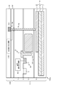
- Each pixel area PR may be configured, for example, as shown in FIG.
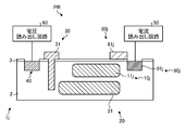
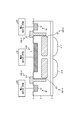
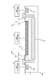
- FIG. 1 is a cross-sectional view showing the configuration of one pixel region PR in the solid-state image sensor 1.
- the interlayer insulating film is not shown for the sake of simplicity.
- the pixel region PR of the solid-state image sensor 1 includes a photoelectric conversion unit 10, a photoelectric conversion unit 20, a transfer unit 30, and a charge-voltage conversion unit 40.
- the photoelectric conversion unit 10 has a semiconductor region 11.
- the semiconductor region 11 is arranged near the surface of the semiconductor substrate 2, and the surface 11a thereof constitutes a part of the surface of the semiconductor substrate 2.
- the surface of the semiconductor substrate 2 is generally covered with the gate insulating film 3, but the surface 11a of the semiconductor region 11 is not covered with the gate insulating film 3 and is exposed to the interlayer insulating film (not shown).
- the semiconductor substrate 2 contains a first conductive type (for example, P type) impurity at a first concentration.
- the P-type impurity is, for example, boron.
- the semiconductor region 11 contains impurities of the second conductive type (for example, N type) at a second concentration higher than the first concentration.
- N-type impurities are, for example, phosphorus or arsenic.
- the second conductive type is an opposite conductive type of the first conductive type.
- the photoelectric conversion unit 10 receives light, performs photoelectric conversion on the received light in the interface region between the semiconductor region 11 and the semiconductor substrate 2, and responds to the light. A charge is generated and led to the semiconductor region 11.
- the photoelectric conversion unit 10 functions as a photodiode, for example.
- the photoelectric conversion unit 10 is a photoelectric conversion unit for DVS, and the current readout circuit 50 is electrically connected to the photoelectric conversion unit 10. The electric charge introduced to the semiconductor region 11 is read out to the current reading circuit 50 as a current.
- the current readout circuit 50 is a current / logarithmic voltage conversion type circuit, and is an event detection circuit that detects a change in current as an event.
- the current readout circuit is, for example, a DVS circuit.
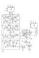
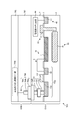
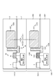
- the current readout circuit 50 may be configured, for example, as shown in FIG. FIG. 2 is a diagram showing a configuration of a current readout circuit 50 and a voltage readout circuit 60 in the solid-state image sensor 1.
- the current readout circuit 50 includes a current / logarithmic voltage conversion unit 51, a buffer 52, a differentiating circuit 53, and a comparator 54.
- the current / logarithmic voltage conversion unit 51 logarithmically converts the current (photocurrent) read from the photoelectric conversion unit 10 into a voltage.
- the photoelectric conversion unit 10 has a photodiode D10.
- the current / logarithmic voltage conversion unit 51 includes N-type transistors TR511 and TR513 and a P-type transistor TR512.
- the N-type transistor TR511 is, for example, an MFP transistor, the source is electrically connected to the cathode of the photodiode D10 via the node N511, the drain is electrically connected to the power potential, and the gate is electrically connected to the node N512. It is connected.
- the P-type transistor TR512 is, for example, a polyclonal transistor, the source is electrically connected to the power potential, the drain is electrically connected to the node N512, and the gate receives a bias voltage from a control circuit (not shown). ..
- the N-type transistor TR513 is, for example, an MFP transistor, the source is electrically connected to the ground potential, the drain is electrically connected to the node N512, and the gate is electrically connected to the cathode of the photodiode D10 via the node N511. It is connected. Node N512 is electrically connected to buffer 52.
- the buffer 52 buffers a signal corresponding to the voltage of the current / logarithmic voltage conversion unit 51.
- the buffer 52 has an N-type transistor TR521 and a current source CS521.
- the N-type transistor TR521 is, for example, an MFP transistor, the source is electrically connected to one end of the current source CS521 via the node N521, the drain is electrically connected to the power potential, and the gate is electrically connected to the node N512. It is connected.
- One end of the current source CS521 is electrically connected to the node N521, and the other end is electrically connected to the ground potential.
- the node N521 is electrically connected to the differentiating circuit 53.
- the differentiating circuit 53 performs a differentiating operation on the signal buffered by the buffer 52, and generates a differentiating signal corresponding to the amount of change in the current.
- the differentiating circuit 53 includes capacitive elements C531, C532, P-type transistors TR531, TR532, and a current source CS531.
- One end of the capacitive element C531 is electrically connected to the node N521, and the other end is electrically connected to the node N531.
- One end of the capacitive element C532 is electrically connected to the node N531 and the other end is electrically connected to the node N532.
- the P-type transistor TR531 is, for example, a polyclonal transistor, in which the source is electrically connected to the power potential, the drain is electrically connected to the node N532, and the gate is electrically connected to the node N531.
- the P-type transistor TR532 is, for example, a polyclonal transistor, the source of which is electrically connected to the node N531 and the drain of which is electrically connected to one end of the node N532 and the current source CS531 from a control circuit (not shown) at the gate. Receives the bias voltage of.
- One end of the current source CS531 is electrically connected to the node N532, and the other end is electrically connected to the ground potential.
- the node N532 is electrically connected to the comparator 54.
- the comparator 54 compares the differential signal generated by the differentiating circuit 53 with a predetermined threshold value, and generates a signal indicating the presence or absence of an event according to the comparison result.
- the comparator 54 has P-type transistors TR541 and TR542 and N-type transistors TR543 and TR544.
- the P-type transistor TR541 is, for example, a polyclonal transistor, in which the source is electrically connected to the power potential, the drain is electrically connected to the node N541, and the gate is electrically connected to the node N532.
- the P-type transistor TR542 is, for example, a polyclonal transistor, in which the source is electrically connected to the power potential, the drain is electrically connected to the node N542, and the gate is electrically connected to the node N532.
- the N-type transistor TR543 is, for example, an MFP transistor, the source is electrically connected to the ground potential, the drain is electrically connected to the node N541, and the gate receives a bias voltage V1 from a control circuit (not shown).
- the N-type transistor TR544 is, for example, an MFP transistor, the source is electrically connected to the ground potential, the drain is electrically connected to the node N542, and the gate receives a bias voltage V2 from a control circuit (not shown). ..
- the bias voltage V1 corresponds to the upper limit of the fluctuation range of the differential signal
- the bias voltage V2 corresponds to the lower limit of the fluctuation range of the differential signal.
- the comparator 54 supplies the high-level CM1 to the logic circuit 71 as a signal indicating the occurrence of an event on the upper limit side.
- the comparator 54 supplies the low-level CM2 to the logic circuit 71 as a signal indicating the occurrence of an event on the lower limit side.
- the photoelectric conversion unit 20 is an embedded type and has a semiconductor region 21.
- the semiconductor region 21 is arranged at a position deeper than the surface of the semiconductor substrate 2 and is arranged at a position deeper than the semiconductor region 11.
- the semiconductor region 21 overlaps the semiconductor region 11 when viewed from the incident direction of light. Assuming that the axis extending in the direction perpendicular to the surface of the semiconductor substrate 2 through the center of the semiconductor region 11 is the optical axis PX11 of the semiconductor region 11, the optical axis PX11 of the semiconductor region 11 intersects the semiconductor region 21.
- the optical axis PX21 of the semiconductor region 21 intersects the semiconductor region 11.
- the semiconductor region 21 is separated from the semiconductor region 11 in the depth direction.
- the semiconductor region 21 contains a second conductive type (for example, N type) impurity at a third concentration higher than the first concentration and lower than the second concentration.
- the photoelectric conversion unit 20 receives light, performs photoelectric conversion on the received light in the interface region between the semiconductor region 21 and the semiconductor substrate 2, and responds to the light. Charges are generated and accumulated in the semiconductor region 21.
- the photoelectric conversion unit 20 since the photoelectric conversion unit 20 is an embedded type, the influence of the trap level on the surface of the semiconductor substrate 2 can be suppressed, and noise charges can be suppressed from being mixed in the charges accumulated in the semiconductor region 21.
- the photoelectric conversion unit 20 functions as, for example, the photodiode D20 shown in FIG.
- the transfer unit 30 shown in FIG. 1 transfers the charge stored in the photoelectric conversion unit 20 to the charge voltage conversion unit 40.
- the charge-voltage conversion unit 40 converts the transferred charge into a voltage.
- the charge-voltage conversion unit 40 functions as, for example, a floating diffusion FD (see FIG. 2) and has a semiconductor region 41.
- the semiconductor region 41 is arranged near the surface of the semiconductor substrate 2, and the surface thereof constitutes a part of the surface of the semiconductor substrate 2.
- the semiconductor region 41 contains a second conductive type (for example, N type) impurities at a second concentration higher than the first concentration.
- the transfer unit 30 functions as, for example, a transfer transistor TR30 (see FIG. 2), and has a semiconductor region 21 as a source, a transfer gate 31 as a gate, and a semiconductor region 41 as a drain.
- the transfer gate 31 is a vertical type extending in the depth direction into the substrate.
- the transfer gate 31 has a flat plate portion 31a that covers the surface of the semiconductor substrate 2 via the gate insulating film 3 and penetrates the gate insulating film 3 from the flat plate portion 31a to penetrate the semiconductor substrate 2 deeper than the semiconductor region 11 in the depth direction. Moreover, it has a trench portion 31b extending to the vicinity of the depth of the semiconductor region 21.
- the transfer gate 31 may be formed of polysilicon containing impurities, or may be formed of a metal such as tungsten.
- the transfer unit 30 transfers the charge accumulated in the semiconductor region 21 to the semiconductor region 41.
- the photoelectric conversion unit 20 is a photoelectric conversion unit for imaging, and the voltage readout circuit 60 is electrically connected via the transfer unit 30 and the charge-voltage conversion unit 40.
- the charge transferred from the semiconductor region 21 to the charge-voltage conversion unit 40 via the transfer unit 30 is converted into a voltage by the charge-voltage conversion unit 40, and the converted voltage is read out to the voltage readout circuit 60.
- the voltage readout circuit 60 is a high impedance input, and is, for example, a source follower type circuit, a source grounded type circuit, or a differential circuit.
- the voltage reading circuit 60 may be, for example, a gradation conversion circuit that converts the read voltage into a signal corresponding to the gradation, an ADC (Analog Digital Conversion) circuit, or a circuit in the stage before the ADC circuit. You may.
- the voltage readout circuit 60 may be configured, for example, as shown in FIG.
- the voltage readout circuit 60 has an amplification unit 61, a selection unit 62, and a reset unit 63.
- the selection unit 62 switches the voltage readout circuit 60 between the selected state and the non-selected state.
- the selection unit 62 has a selection transistor SEL.
- the selection transistor SEL selects the voltage readout circuit 60 when the active level control signal is received at the gate, and deselects the voltage readout circuit 60 when the non-active level control signal is received at the gate.
- the amplification unit 61 amplifies the voltage of the charge-voltage conversion unit 40 when the voltage readout circuit 60 is in the selected state.
- the amplification unit 61 has an amplification transistor AMP.
- the amplification transistor AMP performs a source follower operation together with a current source (not shown) connected to the signal line SL according to the voltage of the charge-voltage conversion unit 40, and outputs a signal corresponding to the voltage of the charge-voltage conversion unit 40 to the signal line. Supply to SL.
- the reset unit 63 resets the voltage of the charge-voltage conversion unit 40.
- the reset unit 63 has a reset transistor RST.
- the reset transistor RST discharges the charge held in the charge-voltage conversion unit 40 to the power supply potential when the active level control signal is received at the gate, and resets the voltage of the charge-voltage conversion unit 40.
- a plurality of voltage readout circuits 60 corresponding to a plurality of pixel region PRs arranged in a column direction among a plurality of pixel region PRs arranged two-dimensionally are connected to the signal line SL, and the plurality of voltage readout circuits 60 are connected.
- the ADC circuit 72 may be connected to the signal line SL.
- the ADC circuit 72 AD-converts a pixel signal (analog signal) to generate a pixel signal (digital signal), and supplies the pixel signal (digital signal) to the logic circuit 73 as a signal indicating a gradation value.
- the logic circuit 73 performs imaging processing by forming image data according to pixel signals of a plurality of pixel region PRs and performing predetermined image processing.
- the photoelectric conversion unit 20 is a photoelectric conversion unit for imaging, and it is required to improve the image quality of the obtained image and improve the S / N ratio. Is required, so it is composed of an embedded type. Since the photoelectric conversion unit 10 is a photoelectric conversion unit for DVS and is required to have higher sensitivity than image quality, it does not have to be an embedded type and may be configured to be exposed on the surface of the semiconductor substrate 2.
- connection form between the photoelectric conversion unit 10 and the current readout circuit 50 and the connection form between the photoelectric conversion unit 20 and the voltage readout circuit 60 are different from each other.
- the photoelectric conversion unit 10 is directly connected to the current readout circuit 50, and is electrically connected to the gate of the transistor TR513 (see FIG. 2) in the current readout circuit 50.
- the photoelectric conversion unit 20 is connected to the voltage readout circuit 60 via the transfer unit 30 and the charge-voltage conversion unit 40, and is electrically connected to the voltage readout circuit 60 via the source and drain of the transistor TR30.
- the transistor TR30 is a vertical type in which the transfer gate 31 extends in the depth direction into the substrate.
- the semiconductor substrate 2 may have a semiconductor region 4 formed in the vicinity of the boundary in order to be electrically separated from the other pixel region PR.
- the semiconductor region 4 contains impurities of the first conductive type (for example, P type) at a fourth concentration higher than the first concentration.
- the semiconductor region 4 may form a potential barrier for electric charges (for example, electrons) in the vicinity thereof.
- each pixel region PR of the solid-state image sensor 1 a plurality of photoelectric conversion units 10 and 20 are arranged so as to be overlapped with each other in the incident direction of light. As a result, in each pixel region PR, a large area can be secured in the plane direction of the photoelectric conversion units 10 and 20 having different uses. Further, in each pixel region PR of the solid-state image sensor 1, a plurality of photoelectric conversion units 10 and 20 are connected to different types of readout circuits 50 and 60. As a result, the plurality of photoelectric conversion units 10 and 20 can be controlled independently of each other. Therefore, the aperture ratio of each photoelectric conversion unit 10 and 20 can be easily secured while controlling the photoelectric conversion units 10 and 20 having different uses independently of each other.
- color filter is omitted for the sake of simplification of illustration and explanation, it may be the same color, a color filter arranged in Bayer, a complementary color filter, or the like, and various forms of color may be used. Filters can be applied.
- FIG. 3 is a cross-sectional view showing the configuration of the solid-state image sensor 1i according to the first modification of the first embodiment of the present disclosure.
- the pixel region PR of the solid-state image sensor 1i has a photoelectric conversion unit 10i instead of the photoelectric conversion unit 10 (see FIG. 1).
- the photoelectric conversion unit 10i has a semiconductor region 11i and a semiconductor region 12i in place of the semiconductor region 11 (see FIG. 1).
- the semiconductor region 11i is arranged near the surface of the semiconductor substrate 2, and the surface 11ia constitutes a part of the surface of the semiconductor substrate 2.
- the surface of the semiconductor substrate 2 is generally covered with the gate insulating film 3, but the surface 11ia of the semiconductor region 11i is not covered with the gate insulating film 3 and is exposed to the interlayer insulating film (not shown).
- the semiconductor region 11i contains impurities of the second conductive type (for example, N type) at a second concentration higher than the first concentration.
- the semiconductor region 12i is arranged at a position deeper than the surface of the semiconductor substrate 2 and slightly deeper than the semiconductor region 11i.
- the semiconductor region 12i is joined to the semiconductor region 11i.
- the semiconductor region 12i contains the second conductive type impurities at a third concentration higher than the first concentration and lower than the second concentration.
- Both the semiconductor region 11i and the semiconductor region 12i are arranged at positions shallower than the semiconductor region 21 and separated from the semiconductor region 21 in the depth direction.
- the semiconductor region 11i and the semiconductor region 12i each overlap the semiconductor region 21 when viewed from the incident direction of light.
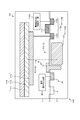
- FIG. 4 is a cross-sectional view showing the configuration of the solid-state image sensor 1j according to the second modification of the first embodiment of the present disclosure.
- the pixel region PR of the solid-state image sensor 1j has a photoelectric conversion unit 10j instead of the photoelectric conversion unit 10 (see FIG. 1), and further includes a transfer unit 80j and a buffer unit 90j.
- the photoelectric conversion unit 10j is an embedded type and has a semiconductor region 11j.
- the semiconductor region 11j is arranged at a position deeper than the surface of the semiconductor substrate 2 and at a position shallower than the semiconductor region 21.
- the semiconductor region 11j overlaps the semiconductor region 21 when viewed from the incident direction of light.
- the semiconductor region 11j is separated from the semiconductor region 21 in the depth direction.
- the semiconductor region 11j contains impurities of the second conductive type (for example, N type) at a third concentration higher than the first concentration and lower than the second concentration.
- the transfer unit 80j transfers the electric charge accumulated in the photoelectric conversion unit 10j to the buffer unit 90j.
- the buffer unit 90j buffers the transferred electric charge.
- the electric charge buffered in the buffer unit 90j is read out to the current reading circuit 50 as a current (photocurrent).
- the buffer unit 90j has a semiconductor region 91j.
- the semiconductor region 91j contains a second conductive type (for example, N type) impurity at a first concentration.
- the transfer unit 80j functions as, for example, a transfer transistor, and has a semiconductor region 11j as a source, a transfer gate 81j as a gate, and a semiconductor region 91j as a drain.
- the transfer gate 81j is a planar type extending in a plane direction along the surface of the substrate. When the active level control signal is supplied to the transfer gate 81j, the transfer unit 80j transfers the charge accumulated in the semiconductor region 11j to the semiconductor region 91j.
- connection form between the photoelectric conversion unit 10j and the current readout circuit 50 and the connection form between the photoelectric conversion unit 20 and the voltage readout circuit 60 are different from each other.
- the photoelectric conversion unit 10j is connected to the current readout circuit 50 via the source and drain of the transfer transistor including the planar type transfer gate 81j.
- the photoelectric conversion unit 20 is electrically connected to the voltage readout circuit 60 via the source and drain of the transfer transistor including the vertical transfer gate 31. That is, the transfer transistor of the transfer unit 80j can form a channel region at a shallow position corresponding to the semiconductor region 11j, and the transfer transistor of the transfer unit 30 can form a channel region including a deep position corresponding to the semiconductor region 21.
- the charges of the photoelectric conversion units 10j and 20 can be read out independently.
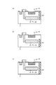
- the solid-state image sensor 1 may be a front-illuminated type as shown in FIG. 5 (a) or a back-illuminated type as shown in FIG. 5 (b).
- FIG. 5 is a cross-sectional view showing the configuration of the solid-state image sensor 1 according to the third modification of the first embodiment of the present disclosure.
- the photoelectric conversion unit 10 for DVS has R (red) light and G (green) light. , B (blue) light and IR (infrared) light may be received.
- the photoelectric conversion unit 20 for imaging may be capable of receiving IR light, may be capable of receiving R light and IR light, and may receive either R light or G light and IR light. It may be possible.
- the photoelectric conversion unit 10 for DVS and the photoelectric conversion unit 20 for imaging may be capable of receiving light having different wavelengths depending on the depth from the surface of the substrate.
- the photoelectric conversion unit 10 for DVS may be capable of receiving IR light in each pixel region PR of the solid-state image sensor 1. , R light and IR light may be received.
- the photoelectric conversion unit 20 for imaging may be capable of receiving any one of R light, G light, and B light and IR light.
- the photoelectric conversion unit 10 for DVS and the photoelectric conversion unit 20 for imaging may be capable of receiving light having different wavelengths depending on the depth from the back surface of the substrate.
- the aperture ratios of the photoelectric conversion units 10 and 20 having different uses can be easily secured in each pixel region PR.
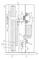
- FIG. 6 is a cross-sectional view showing the configuration of the solid-state image sensor 1k according to the fourth modification of the first embodiment of the present disclosure.
- the pixel region PR of the solid-state image sensor 1k has a photoelectric conversion unit 20k and a transfer unit 30k in place of the photoelectric conversion unit 20 and the transfer unit 30 (see FIG. 1).
- the photoelectric conversion unit 20k is an embedded type and has a semiconductor region 21k.
- the semiconductor region 21k has a flat plate portion 21k1 and a drawing portion 21k2.
- the flat plate portion 21k1 is arranged at a position deeper than the surface of the semiconductor substrate 2 and is arranged at a position deeper than the semiconductor region 11.
- the flat plate portion 21k1 overlaps the semiconductor region 11 when viewed from the incident direction of light.
- the flat plate portion 21k1 is separated from the semiconductor region 11 in the depth direction.
- the lead-out portion 21k2 extends from the end portion of the flat plate portion 21k1 on the semiconductor region 41 side to the vicinity of the surface of the semiconductor substrate 2 in the depth direction.
- the lead-out portion 21k2 is separated from the semiconductor region 11 in the plane direction.
- the flat plate portion 21k1 and the drawing portion 21k2 each contain impurities of the second conductive type (for example, N type) at a third concentration higher than the first concentration and lower than the second concentration.
- the transfer unit 30k functions as, for example, a transfer transistor TR30 (see FIG. 2), and has a semiconductor region 21k as a source, a transfer gate 31k as a gate, and a semiconductor region 41 as a drain.
- the transfer gate 31k is a planar type extending in a plane direction along the surface of the substrate.
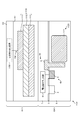
- FIG. 7 is a cross-sectional view showing the configuration of the solid-state image sensor 1n according to the fifth modification of the first embodiment of the present disclosure.
- the pixel region PR of the solid-state image sensor 1n further includes a charge holding unit 140n and a transfer unit 130n.
- the charge holding unit 140n is an embedded type and has a semiconductor region 141n.
- the semiconductor region 141n is arranged at a position deeper than the surface of the semiconductor substrate 2 and at a position shallower than the semiconductor region 21.
- the semiconductor region 11j contains impurities of the second conductive type (for example, N type) at a third concentration higher than the first concentration and lower than the second concentration.
- the transfer unit 30 transfers the charge accumulated in the photoelectric conversion unit 20 to the charge holding unit 140n.
- the charge holding unit 140n holds the transferred charge.
- the transfer unit 130n transfers the charge held by the charge holding unit 140n to the charge-voltage conversion unit 40.
- the transfer unit 130n functions as a transfer transistor inserted in series between, for example, the transfer transistor TR30 and the floating diffusion FD, and has a semiconductor region 141n as a source, a transfer gate 131n as a gate, and a semiconductor region 41 as a drain. ..
- the transfer gate 131n is a planar type extending in a plane direction along the surface of the substrate. When the active level control signal is supplied to the transfer gate 131n, the transfer unit 130n transfers the charge held in the semiconductor region 141n to the semiconductor region 41.
- the charge storage operation of the photoelectric conversion unit 20 is simultaneously performed for the plurality of pixel region PRs, and the charge voltage is charged from the charge holding unit 140n. It is possible to realize a global shutter operation in which electric charges are sequentially transferred to the conversion unit 40. Alternatively, it is possible to realize an operation of switching the charge of the charge holding unit 140n to the charge voltage conversion unit 40 and / or another charge voltage conversion unit (not shown) so that the charge can be transferred and the conversion efficiency of the charge voltage conversion can be changed. be.
- connection form between the photoelectric conversion unit 10 and the current readout circuit 50 and the connection form between the photoelectric conversion unit 20 and the voltage readout circuit 60 are different from each other.
- the photoelectric conversion unit 10 is directly connected to the current readout circuit 50.
- the photoelectric conversion unit 20 is electrically connected to the voltage readout circuit 60 via the source and drain of the transfer transistor including the vertical transfer gate 31 and the source and drain of the transfer transistor including the planar type transfer gate 131n. ing.
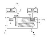
- the first embodiment focuses on the cross-sectional configuration of each pixel region PR of the solid-state image sensor, while the second embodiment focuses on the planar configuration of each pixel region PR of the solid-state image sensor.
- the photoelectric conversion unit 10 has a semiconductor region 11.
- the semiconductor region 11 is arranged near the surface of the semiconductor substrate 2, and the surface thereof constitutes a part of the surface of the semiconductor substrate 2.
- the photoelectric conversion unit 20 is an embedded type and has a semiconductor region 21.
- the semiconductor region 21 is arranged at a position deeper than the surface of the semiconductor substrate 2 and at a position deeper than the semiconductor region 11.
- the semiconductor region 11 and the semiconductor region 21 are arranged so that at least their main portions overlap each other.
- the semiconductor region 11 may be included inside the semiconductor region 21.
- the light receiving area of each photoelectric conversion unit 10 and 20 can be easily secured.
- a margin of layout area can be provided in the pixel area PR.
- the photoelectric conversion unit 10 is a photoelectric conversion unit for DVS, and the current readout circuit 50 is electrically connected to the photoelectric conversion unit 10.
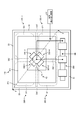
- the photoelectric conversion unit 20 is a photoelectric conversion unit for imaging, a photoelectric conversion unit for imaging, and a voltage readout circuit 260 is electrically connected via a transfer unit 30 and a charge-voltage conversion unit 40.
- the transfer gate 31 of the transfer unit 30 is arranged at a position adjacent to the semiconductor region 21.
- the semiconductor region 41 of the charge-voltage conversion unit 40 is arranged on the opposite side of the semiconductor region 21 with the transfer gate 31 in between.
- the element group of the voltage readout circuit 260 may be arranged in the pixel area PR. This makes it possible to efficiently lay out the voltage readout circuit 260.
- the voltage readout circuit 260 has an amplification unit 261 and a selection unit 262, and a reset unit 263.
- the amplification unit 261 functions as, for example, an amplification transistor AMP (see FIG. 2), and has a semiconductor region 61s as a source, an electrode 61g as a gate, and a semiconductor region 61d as a drain.
- the selection unit 262 functions as, for example, a selection transistor SEL (see FIG. 2), and has a semiconductor region 62s as a source, an electrode 62g as a gate, and a semiconductor region 61s as a drain.
- the semiconductor region 61s is shared by the amplification unit 261 and the selection unit 262.
- the reset unit 263 functions as, for example, a reset transistor RST (see FIG. 2), and has a semiconductor region 63s as a source, an electrode 63 g as a gate, and a semiconductor region 61d as a drain.
- the semiconductor region 61d is shared by the amplification unit 261 and the reset unit 263.
- each pixel region PR of the solid-state image sensor 201 a plurality of photoelectric conversion units 10 and 20 are arranged so as to overlap each other in the incident direction of light.
- the light receiving area of each photoelectric conversion unit 10 and 20 can be easily secured, and the aperture ratio of each photoelectric conversion unit 10 and 20 can be easily secured.
- FIG. 9 is a plan view showing the configuration of the solid-state image sensor 201i according to the first modification of the second embodiment of the present disclosure.
- FIG. 9 illustrates a case where two electrodes and three semiconductor regions corresponding to two transistors (for example, the transistors TR513 and TR512 shown in FIG. 2) in the current readout circuit 250i are arranged in the pixel region PR. ..
- FIG. 10 is a plan view showing the configuration of the solid-state image sensor 201j according to the second modification of the second embodiment of the present disclosure.
- three electrodes and four semiconductor regions corresponding to three further transistors for example, transistors TR511, TR5211, TR532, etc. shown in FIG. 2 in the current readout circuit 250j are in the pixel region PR. The case where it is additionally distributed to is illustrated.
- the pixel region PR of the solid-state image sensor 201 may be element-separated from another pixel region PR via the insulation separation unit DI.
- the insulation separation portion DI can be formed of a material containing an insulator such as silicon oxide as a main component.
- FIG. 11 is a plan view showing the configuration of the solid-state image sensor 201 according to the third modification of the second embodiment of the present disclosure, and illustrates one pixel region PR.
- the insulation separation unit DI shown in FIG. 11 extends along the outer edge of the pixel region PR and surrounds the pixel region PR. When the pixel region PR is rectangular in a plan view, the insulation separation unit DI surrounds the pixel region PR in a rectangular shape.
- the insulation separation unit DI may be configured as a DTI (Deep Trench Isolation) type as shown in FIG. 12 (a).
- FIG. 12 is a cross-sectional view showing the configuration of the solid-state image sensor 201 according to the second modification of the second embodiment of the present disclosure, and shows a cross-sectional view when FIG. 11 is cut along the line AA.
- the insulation separation unit DI shown in FIG. 12A may extend from the surface of the semiconductor substrate 2 to a depth corresponding to the depth of the semiconductor region 21 in the depth direction. As a result, it is possible to suppress the electric charge accumulated in the semiconductor region 21 from leaking to the adjacent pixel region PR, and it is possible to suppress the color mixing between the adjacent pixel region PR.
- the insulation separation unit DI may be configured as an RDTI (Reverse Deep Trench Isolation) type as shown in FIG. 12 (b). That is, the insulation separation unit DI may extend from a depth shallower than the semiconductor region 21 to the back surface of the semiconductor substrate 2 in the depth direction. This also suppresses the leakage of the electric charge accumulated in the semiconductor region 21 to the adjacent pixel region PR, and suppresses the color mixing between the adjacent pixel region PR.
- RDTI Reverse Deep Trench Isolation
- the insulation separation unit DI may be configured as an FDTI (Full Deep Trench Isolation) type as shown in FIG. 12 (c). That is, the insulation separation unit DI may extend from the front surface of the semiconductor substrate 2 to the back surface of the semiconductor substrate 2 in the depth direction. This also suppresses the leakage of the electric charge accumulated in the semiconductor region 21 to the adjacent pixel region PR, and suppresses the color mixing between the adjacent pixel region PR.
- FDTI Frel Deep Trench Isolation
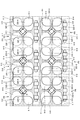
- FIG. 13 is a plan view showing the configuration of the solid-state image sensor 201 according to the second modification of the second embodiment of the present disclosure, and illustrates a plurality of pixel region PRs.
- the insulation separation unit DI extends in a grid pattern in a plan view and partitions a plurality of pixel region PRs.
- a plurality of photoelectric conversion units 10 and 20 are arranged so as to overlap each other in the incident direction of light, which is the same as the second embodiment. This makes it possible to suppress color mixing between adjacent pixel region PRs.
- each pixel region PR In the first embodiment and the second embodiment, a configuration in which one photoelectric conversion unit for different purposes is arranged in each pixel region PR is illustrated, but in the third embodiment, each pixel region is illustrated.
- An example is a configuration in which a plurality of photoelectric conversion units for different purposes are arranged in the PR.
- the pixel region PR of the solid-state image sensor 301 has a plurality of photoelectric conversion units 310 instead of the photoelectric conversion unit 10, the photoelectric conversion unit 20, and the transfer unit 30 (see FIG. 1). It has -1 to 310-4, a plurality of photoelectric conversion units 320-1 to 320-4, and a plurality of transfer units 330-1 to 330-4.
- FIG. 14 is a plan view showing the configuration of the solid-state image sensor 301 according to the third embodiment of the present disclosure.
- Each of the plurality of photoelectric conversion units 310-1 to 310-4 has a semiconductor region 311. As shown by the solid line in FIG. 14, the semiconductor region 311 is arranged near the surface of the semiconductor substrate 2, and the surface thereof constitutes a part of the surface of the semiconductor substrate 2. Each of the plurality of photoelectric conversion units 320-1 to 320-4 is an embedded type and has a semiconductor region 321. As shown by the dotted line in FIG. 14, the semiconductor region 321 is arranged at a position deeper than the surface of the semiconductor substrate 2 and at a position deeper than the semiconductor region 311. The semiconductor region 311 may be included inside the semiconductor region 321 when viewed from the incident direction of light.
- the plurality of photoelectric conversion units 310-1 to 310-4 correspond to the plurality of photoelectric conversion units 320-1 to 320-4.
- the optical axis of each photoelectric conversion unit 310 intersects the corresponding photoelectric conversion unit 320.
- the optical axis of each photoelectric conversion unit 320 intersects the corresponding photoelectric conversion unit 310.
- the plurality of transfer units 330-1 to 330-4 correspond to a plurality of photoelectric conversion units 320-1 to 320-4.
- the transfer gate 331 of each transfer unit 330 is arranged at a position adjacent to the semiconductor region 321.
- the semiconductor region 41 of the charge-voltage conversion unit 40 is arranged on the opposite side of the semiconductor region 321 with the transfer gate 331 in between.
- Each transfer unit 330 functions as, for example, a transfer transistor TR30 (see FIG. 2), and has a semiconductor region 321 as a source, a transfer gate 331 as a gate, and a semiconductor region 41 as a drain. That is, the semiconductor region 41 of the charge-voltage conversion unit 40 is shared by the plurality of transfer units 330-1 to 330-4, and is shared by the plurality of photoelectric conversion units 320-1 to 320-4 via the transfer unit 330. Has been done. That is, a common charge-voltage conversion unit 40 is provided for the plurality of photoelectric conversion units 320-1 to 320-4.
- the transfer gate 331 of each transfer unit 330 may be configured in a vertical shape.
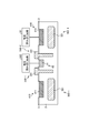
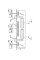
- FIG. 15 is a cross-sectional view showing the configuration of the solid-state image sensor according to the third embodiment of the present disclosure, and shows a cross-sectional view when FIG. 14 is cut along the line BB.
- the transfer gate 331 is a vertical type extending in the depth direction into the substrate.
- the transfer gate 331 penetrates the flat plate portion 331a that covers the surface of the semiconductor substrate 2 via the gate insulating film 3 and the gate insulating film 3 from the flat plate portion 331a, and is deeper than the semiconductor region 311 in the semiconductor substrate 2 in the depth direction. Moreover, it has a trench portion 331b extending to the vicinity of the depth of the semiconductor region 321.
- the transfer gate 331 may be formed of polysilicon containing impurities, or may be formed of a metal such as tungsten.
- the transfer unit 330 transfers the charge accumulated in the semiconductor region 321 of the corresponding photoelectric conversion unit 320 to the semiconductor region 41.
- connection form between the photoelectric conversion unit 310 and the current readout circuit 50 and the connection form between the photoelectric conversion unit 320 and the voltage readout circuit 260 are different from each other.
- the plurality of photoelectric conversion units 310-1 to 310-4 correspond to a plurality of current readout circuits 50.
- Each photoelectric conversion unit 310 is directly connected to the corresponding current readout circuit 50.
- the plurality of photoelectric conversion units 320 are connected to the common voltage readout circuit 260 via the corresponding transfer unit 330 and the common charge-voltage conversion unit 40.
- a plurality of photoelectric conversion units 310-1 to 310-4 and a plurality of photoelectric conversion units 320-1 to 320-4 are provided in each pixel region PR of the solid-state image sensor 301. Arrange them so that they overlap in the incident direction of the light. As a result, the light receiving area of each photoelectric conversion unit 310, 320 can be easily secured, and the aperture ratio of each photoelectric conversion unit 310, 320 can be easily secured.
- a configuration in which a plurality of photoelectric conversion units are arranged for DVS in the pixel region PR is illustrated, but in the fourth embodiment, with respect to the configuration of the third embodiment,
- An example is a configuration in which a plurality of photoelectric conversion units are shared for DVS in the pixel region PR. This makes it possible to improve the sensitivity of the photoelectric conversion unit for DVS.
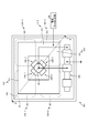
- FIG. 16 is a plan view showing the configuration of the solid-state image sensor 401 according to the fourth embodiment of the present disclosure.
- the photoelectric conversion unit 410 corresponds to a photoelectric conversion unit in which a plurality of photoelectric conversion units 310-1 to 310-4 are shared, and has a semiconductor region 411.
- the semiconductor region 411 extends in a donut shape at positions corresponding to a plurality of photoelectric conversion units 320-1 to 320-4.
- the semiconductor region 411 surrounds a plurality of transfer units 330-1 to 330-4 and a charge-voltage conversion unit 40.
- the configuration of FIG. 16 can be regarded as sharing the plurality of photoelectric conversion units 310 with respect to the configuration of FIG. 14 so as to surround the plurality of transfer units 330-1 to 330-4 and the charge / voltage conversion unit 40.
- the semiconductor region 411 is arranged near the surface of the semiconductor substrate 2, and the surface thereof constitutes a part of the surface of the semiconductor substrate 2.
- the semiconductor region 411 overlaps each of the main portions of the semiconductor region 321 of the plurality of photoelectric conversion units 320-1 to 320-4.
- the optical axis PX321 of each photoelectric conversion unit 320-1 to 320-4 intersects the photoelectric conversion unit 410.
- the photoelectric conversion unit 410 can secure a large light receiving area and improve its sensitivity.
- the plurality of photoelectric conversion units 320-1 to 320-4 can secure the number and improve the resolution, and can also secure the light receiving area of each photoelectric conversion unit 320 by sharing the charge-voltage conversion unit 40 and the like. That is, when the photoelectric conversion unit 410 and the plurality of photoelectric conversion units 320 for different purposes are arranged in the pixel region PR, the light receiving areas of the photoelectric conversion units 410 and 320 can be secured according to the application.
- the transfer gate 331 of each transfer unit 330 may be configured in a vertical shape, as in the third embodiment.
- FIG. 17 is a cross-sectional view showing the configuration of the solid-state image sensor according to the fourth embodiment of the present disclosure, and shows a cross-sectional view when FIG. 16 is cut along the line CC.
- the transfer gate 331 is a vertical type extending in the depth direction into the substrate.
- connection form between the photoelectric conversion unit 410 and the current readout circuit 50 and the connection form between the photoelectric conversion unit 320 and the voltage readout circuit 260 are different from each other.
- the photoelectric conversion unit 410 is directly connected to the current readout circuit 50.
- the plurality of photoelectric conversion units 320 are connected to the common voltage readout circuit 260 via the corresponding transfer unit 330 and the common charge-voltage conversion unit 40.
- the photoelectric conversion unit 410 and the plurality of photoelectric conversion units 320-1 to 320-4 are arranged so as to overlap each other in the incident direction of light. do.
- the light receiving area of each photoelectric conversion unit 410, 320 can be easily secured, and the aperture ratio of each photoelectric conversion unit 410, 320 can be easily secured.
- the pixel region PR of the solid-state image sensor 401 may be element-separated from the other pixel region PR via the insulation separation unit DI.
- the insulation separation portion DI can be formed of a material containing an insulator such as silicon oxide as a main component.
- FIG. 18 is a plan view showing the configuration of the solid-state image sensor 401 according to the first modification of the fourth embodiment of the present disclosure, and illustrates one pixel region PR.
- the insulation separation unit DI shown in FIG. 18 extends along the outer edge of the pixel region PR and surrounds the pixel region PR. When the pixel region PR is rectangular in a plan view, the insulation separation unit DI surrounds the pixel region PR in a rectangular shape.
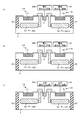
- the insulation separation unit DI may be configured as a DTI type as shown in FIG. 19 (a).
- FIG. 19 is a cross-sectional view showing the configuration of the solid-state image sensor 401 according to the first modification of the fourth embodiment of the present disclosure
- FIG. 19A is a cross-sectional view taken along the line DD.
- the cross section of the case is shown. That is, the insulation separation unit DI may extend from the surface of the semiconductor substrate 2 to a depth corresponding to the depth of the semiconductor region 321 in the depth direction. As a result, it is possible to suppress the electric charge accumulated in the semiconductor region 21 from leaking to the adjacent pixel region PR, and it is possible to suppress the color mixing between the adjacent pixel region PR.
- the insulation separation unit DI may be configured as an RDTI type as shown in FIG. 19 (b). That is, the insulation separation unit DI may extend from a depth shallower than the semiconductor region 21 to the back surface of the semiconductor substrate 2 in the depth direction. This also suppresses the leakage of the electric charge accumulated in the semiconductor region 21 to the adjacent pixel region PR, and suppresses the color mixing between the adjacent pixel region PR.
- the insulation separation unit DI may be configured as an FDTI type as shown in FIG. 19 (c). That is, the insulation separation unit DI may extend from the front surface of the semiconductor substrate 2 to the back surface of the semiconductor substrate 2 in the depth direction. This also suppresses the leakage of the electric charge accumulated in the semiconductor region 21 to the adjacent pixel region PR, and suppresses the color mixing between the adjacent pixel region PR.
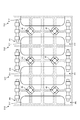
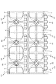
- FIG. 20 is a plan view showing the configuration of the solid-state image sensor 401 according to the first modification of the fourth embodiment of the present disclosure, and illustrates a plurality of pixel region PRs.
- the insulation separation unit DI extends in a grid pattern in a plan view and partitions a plurality of pixel region PRs.
- the photoelectric conversion unit 410 and the plurality of photoelectric conversion units 320 are arranged so as to overlap each other in the incident direction of the light, which is the same as the second embodiment. As a result, the light receiving areas of the photoelectric conversion units 410 and 320 can be easily secured, and the color mixing between the adjacent pixel region PRs can be suppressed.
- the insulation separation unit DI' may be element-separated in units of a plurality of pixel region PRs (for example, in units of two pixel regions).
- 21 (a) and 21 (b) are plan views showing the configuration of the solid-state image sensor 401 according to the second modification of the fourth embodiment of the present disclosure.
- the portion between the two pixel region PRs in the insulation separation unit DI is omitted from the configuration of FIG. 20.
- the photoelectric conversion unit 410' is common to the configuration of FIG. 20 for the two pixel region PRs.
- the light receiving area of the photoelectric conversion unit 410' can be further increased to improve its sensitivity.
- FIG. 22 is a plan view showing the configuration of the solid-state image sensor 401 according to the third modification of the fourth embodiment of the present disclosure, and illustrates one pixel region PR. As shown by the dotted line in FIG.
- the insulation separation unit DI2 extends between the plurality of photoelectric conversion units 320-1 to 320-4 while passing through a position deeper than the charge-voltage conversion unit 40 in the pixel region PR.
- the insulation separation unit DI2 has a plurality of photoelectric conversion units 320-1 to 320 in a substantially cross shape. Extend between -4.
- the insulation separation unit DI2 may be configured as an RDTI type as shown in FIGS. 23 (a) to 23 (c). Further, the insulation separation unit DI may be the DTI type shown in FIG. 23 (a), the RDTI type shown in FIG. 23 (b), or the FDTI type shown in FIG. 23 (c). There may be. 23 (a) to 23 (c) are cross-sectional views showing the configuration of the solid-state image sensor 401 according to the second modification of the fourth embodiment of the present disclosure, and FIG. 22 is taken along the line EE. The cross section when cut is shown.
- the insulation separation unit DI2 is arranged between the semiconductor regions 321 of the plurality of photoelectric conversion units 320 in the plane direction while being separated from the semiconductor region 41 of the charge-voltage conversion unit 40 in the depth direction. As a result, it is possible to suppress the electric charge accumulated in the semiconductor region 321 from leaking to the adjacent semiconductor region 321 in the pixel region PR, and it is possible to suppress the color mixing between the adjacent semiconductor regions 321 in the pixel region PR.
- FIG. 24 is a plan view showing the configuration of the solid-state image sensor 401 according to the fourth modification of the fourth embodiment of the present disclosure, and illustrates one pixel region PR. As shown by the dotted line in FIG.
- the insulation separation unit DI2' is located between the plurality of photoelectric conversion units 320-1 to 320-4 while avoiding the planar position of the semiconductor region 41 of the charge / voltage conversion unit 40 in the pixel region PR. Is extended.
- the insulating separation portion DI2' has a shape in which a portion near the semiconductor region 41 is removed from the substantially cross-shaped insulating separation portion DI2 shown in FIG.
- the insulation separation unit DI2' is separated from the semiconductor region 41 of the charge-voltage conversion unit 40 in the depth direction and the plane direction as shown by the dotted lines in FIGS. 25 (a) to 25 (c), and the RDTI. It may be composed of types. Further, the insulation separation unit DI may be the DTI type shown in FIG. 25 (a), the RDTI type shown in FIG. 25 (b), or the FDTI type shown in FIG. 25 (c). There may be. 25 (a) to 25 (c) are cross-sectional views showing the configuration of the solid-state image sensor 401 according to the fourth modification of the fourth embodiment of the present disclosure, and FIG. 24 is taken along the line FF. The cross section when cut is shown.
- the insulation separation unit DI2' is arranged between the semiconductor regions 321 of the plurality of photoelectric conversion units 320 in the plane direction while being separated from the semiconductor region 41 of the charge-voltage conversion unit 40 in the depth direction and the plane direction. Also by this, it is possible to suppress the electric charge accumulated in the semiconductor region 321 from leaking to the adjacent semiconductor region 321 in the pixel region PR, and it is possible to suppress the color mixing between the adjacent semiconductor regions 321 in the pixel region PR.
- a configuration in which a plurality of photoelectric conversion units are arranged for DVS in the pixel region PR is illustrated, but in the fifth embodiment, with respect to the configuration of the third embodiment,
- An example is a configuration in which a plurality of photoelectric conversion units are shared for DVS across a plurality of pixel region PRs. This makes it possible to improve the sensitivity of the photoelectric conversion unit for DVS.
- the two pixel region PRs of the solid-state image sensor 501 adjacent to each other are 310-3, 310-4 of one pixel region PR and 310-1 of the other pixel region PR. , 310-2 (see FIG. 14), and has a photoelectric conversion unit 510.
- FIG. 26 is a plan view showing the configuration of the solid-state image sensor 501 according to the fifth embodiment of the present disclosure, and illustrates the configuration of the two pixel region PRs.
- the photoelectric conversion unit 510 includes photoelectric conversion units 310-3, 310-4 of one pixel region PR of two adjacent pixel region PRs and photoelectric conversion units 310-1, 310-2 of the other pixel region PR ( (See FIG. 14) corresponds to a common photoelectric conversion unit, and has a semiconductor region 511.
- the semiconductor region 511 is a photoelectric conversion unit 320-3, 320-4 of one pixel region PR of two adjacent pixel region PRs and a photoelectric conversion unit 320-1, 320 of the other pixel region PR.
- the position corresponding to -2 is extended in a substantially rectangular shape.
- the semiconductor region 511 includes a plurality of transfer units 330 and a charge voltage conversion unit 40 of one pixel region PR of two adjacent pixel region PRs, and a plurality of transfer units 330 and a charge voltage conversion unit 40 of the other pixel region PR. It is arranged between and.
- the configuration of FIG. 26 can be regarded as sharing a plurality of photoelectric conversion units 310 arranged among the plurality of charge / voltage conversion units 40 with respect to the configuration of FIG.
- the semiconductor region 511 is arranged near the surface of the semiconductor substrate 2, and the surface thereof constitutes a part of the surface of the semiconductor substrate 2.
- the semiconductor region 511 overlaps each of the main portions of the semiconductor region 321 of the plurality of photoelectric conversion units 320-1 to 320-4.
- the optical axes of the photoelectric conversion units 320-1 to 320-4 intersect the photoelectric conversion unit 510.
- the photoelectric conversion unit 510 can secure a large light receiving area and improve its sensitivity.
- the plurality of photoelectric conversion units 320-1 to 320-4 can secure the number and improve the resolution, and can also secure the light receiving area of each photoelectric conversion unit 320 by sharing the charge-voltage conversion unit 40 and the like. That is, when the photoelectric conversion units 510 and a plurality of photoelectric conversion units 320 for different purposes are arranged in the pixel region PR, the light receiving areas of the photoelectric conversion units 510 and 320 can be secured according to the application.
- the transfer gate 331 of each transfer unit 330 may be configured in a vertical shape, as in the third embodiment.
- FIG. 27 is a cross-sectional view showing the configuration of the solid-state image sensor according to the fifth embodiment of the present disclosure, and shows a cross-sectional view when FIG. 26 is cut along the GG line.
- the transfer gate 331 is a vertical type extending in the depth direction into the substrate.
- connection form between the photoelectric conversion unit 410 and the current readout circuit 50 and the connection form between the photoelectric conversion unit 320 and the voltage readout circuit 260 are different from each other.
- the photoelectric conversion unit 510 is directly connected to the current readout circuit 50.
- the plurality of photoelectric conversion units 320 are connected to the common voltage readout circuit 260 via the corresponding transfer unit 330 and the common charge-voltage conversion unit 40.
- the photoelectric conversion unit 510 and the plurality of photoelectric conversion units 320-1 to 320-4 are arranged so as to overlap each other in the incident direction of light. do.
- the light receiving area of each photoelectric conversion unit 510, 320 can be easily secured, and the aperture ratio of each photoelectric conversion unit 510, 320 can be easily secured.
- the pixel region PR of the solid-state image sensor 501 may be separated from another pixel region PR via the insulation separation unit DI3.
- the insulation separation portion DI3 can be formed of a material containing an insulator such as silicon oxide as a main component.
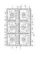
- FIG. 28 is a plan view showing the configuration of the solid-state image sensor 501 according to the first modification of the fifth embodiment of the present disclosure, and illustrates a plurality of pixel region PRs.
- the insulation separation unit DI3 may be configured as an RDTI type as shown by a dotted line in FIG. 28.
- the insulation separation unit DI3 extends in a grid pattern in a plan view, partitions a plurality of pixel region PRs, and extends substantially in a cross shape between the plurality of photoelectric conversion units 320 within each pixel region PR. As a result, color mixing between adjacent pixel region PRs can be suppressed, and color mixing between a plurality of photoelectric conversion units 320 in each pixel region PR can be suppressed.
- FIG. 29 is a plan view showing the configuration of the solid-state image sensor 501 according to the second modification of the fifth embodiment of the present disclosure, and illustrates a plurality of pixel region PRs.
- the element groups of the voltage readout circuit 260 are arranged at positions far from each other between the pixel region RPs adjacent to each other in a direction different from that of the photoelectric conversion unit 510.
- the distances of the semiconductor regions 511 of the plurality of photoelectric conversion units 510 are closer to each other in a direction different from that across the photoelectric conversion units 510 (vertical direction in FIG. 29). can do.
- the solid-state image sensor 501 may have a plurality of photoelectric conversion units 510 that are closer to each other than the configuration of FIG. 29.
- FIG. 30 is a plan view showing the configuration of the solid-state image sensor 501 according to the third modification of the fifth embodiment of the present disclosure, and illustrates a plurality of pixel region PRs.
- the photoelectric conversion unit 510'shown in FIG. 30 is obtained by sharing two photoelectric conversion units 510 arranged in the direction in which the distances are shortened (vertical direction in FIG. 29) in FIG. 29.
- each photoelectric conversion unit 510' has a substantially I shape extending in the vertical direction at a position between the plurality of charge-voltage conversion units 40 in a plan view.
- the solid-state image sensor 501 may further have a plurality of common photoelectric conversion units 510'for the configuration of FIG. 30.
- FIG. 31 is a plan view showing the configuration of the solid-state image sensor 501 according to the fourth modification of the fifth embodiment of the present disclosure, and illustrates a plurality of pixel region PRs.
- the photoelectric conversion unit 510'shown in FIG. 31 is obtained by sharing two photoelectric conversion units 510'arranged in a direction different from the common direction in FIG. 30 (horizontal direction in FIG. 31).
- the semiconductor region 511 "of the conversion unit 510" has a substantially H shape extending a position between the plurality of charge-voltage conversion units 40 in a plan view, whereby the light receiving light of the semiconductor region 511 "of the photoelectric conversion unit 510" is received. A larger area can be secured, and the sensitivity of the photoelectric conversion unit 510 "can be further improved.
- the sixth embodiment illustrates a configuration in which the on-chip lens is provided corresponding to the photoelectric conversion unit 320 for imaging. ..
- each pixel region PR of the solid-state image sensor 501 has a plurality of on-chip lenses 6-1 to 6-4 as shown by the alternate long and short dash line in FIG. 32.
- FIG. 32 is a plan view showing the configuration of the solid-state image sensor 501 according to the sixth embodiment of the present disclosure.
- the plurality of on-chip lenses 6-1 to 6-4 correspond to a plurality of photoelectric conversion units 320-1 to 310-4.
- each on-chip lens 6 is arranged in the incident direction of light with respect to the corresponding photoelectric conversion unit 320.
- FIG. 33 is a cross-sectional view showing the configuration of the solid-state image sensor 501 according to the sixth embodiment of the present disclosure.
- the on-chip lens 6-4 is arranged at a position corresponding to the photoelectric conversion unit 320-4 on the back surface of the insulating film 5 covering the back surface of the semiconductor substrate 2.
- the on-chip lens 6-2 is arranged at a position corresponding to the photoelectric conversion unit 320-2 on the back surface of the insulating film 5.
- the six pixel region PRs are substantially six photoelectric conversion units 510, six ⁇ 4 photoelectric conversion units 320 that overlap the photoelectric conversion unit 510 every four, and the light of the photoelectric conversion unit 320. It has 6 ⁇ 4 on-chip lenses 6 arranged in the incident direction corresponding to the photoelectric conversion unit 320.
- the number of on-chip lenses 6 is the same as the number of photoelectric conversion units 320 for imaging.
- the plurality of photoelectric conversion units 320 of each pixel region PR can easily capture a high-resolution image.
- FIG. 33 illustrates a case where the solid-state image sensor 501 is a back-illuminated type, and the on-chip lens 6 is arranged on the back surface side with respect to the corresponding photoelectric conversion unit 320.
- the on-chip lens 6 is arranged on the surface side with respect to the corresponding photoelectric conversion unit 320, that is, above the semiconductor substrate 2.
- FIG. 34 is a plan view showing the configuration of the solid-state image sensor 501 according to the first modification of the sixth embodiment of the present disclosure.
- each on-chip lens 6' is arranged in the incident direction of light with respect to the corresponding photoelectric conversion unit 510.
- FIG. 35 is a cross-sectional view showing the configuration of the solid-state image sensor 501 according to the sixth embodiment of the present disclosure.
- the on-chip lens 6' is arranged at a position corresponding to the photoelectric conversion unit 510 on the back surface of the insulating film 5 covering the back surface of the semiconductor substrate 2.
- the six pixel region PRs are substantially six photoelectric conversion units 510, six ⁇ 4 photoelectric conversion units 320 overlapping each four photoelectric conversion units 510, and light of the photoelectric conversion unit 510. It has substantially six on-chip lenses 6'arranged corresponding to the photoelectric conversion unit 510 in the incident direction of.
- the number of on-chip lenses 6' is the same as the number of photoelectric conversion units 510 for DVS.
- each photoelectric conversion unit 510 can easily improve its sensitivity.
- the parallax of the plurality of images obtained by reading the pixel signals of the plurality of photoelectric conversion units 320-1 to 310-4 by the voltage readout circuit 260 is detected, and the distance to the subject is determined based on the parallax of the plurality of images. Can be measured.
- the voltage readout circuit 260 is a parallax detection circuit that detects the parallax of a plurality of images, and is a distance measurement circuit that measures the distance to the subject.
- the pixel signals of the plurality of photoelectric conversion units 320-1 to 310-4 overlapping the on-chip lens 6' are added by, for example, the charge-voltage conversion unit 40 and read out by the voltage readout circuit 260 to obtain a signal corresponding to the gradation value. You may get it.
- the voltage readout circuit 260 is a gradation conversion circuit that converts a pixel signal into a gradation value.
- FIG. 35 illustrates a case where the solid-state image sensor 501 is a back-illuminated type, and the on-chip lens 6'is arranged on the back surface side with respect to the corresponding photoelectric conversion unit 510.
- the on-chip lens 6' is arranged on the surface side with respect to the corresponding photoelectric conversion unit 510, that is, above the semiconductor substrate 2.
- the first to sixth embodiments illustrate configurations in which photoelectric conversion units and read circuits thereof having different uses are mounted on one semiconductor chip, but in the seventh embodiment, they are illustrated.
- An example will be given of a configuration in which the configuration is distributed and mounted on a plurality of chips.
- FIG. 36 is a cross-sectional view showing the configuration of the solid-state image sensor 701 according to the seventh embodiment of the present disclosure.
- a plurality of photoelectric conversion units 10 and 20 and a voltage readout circuit 60 for different purposes are arranged on the chip CH1, but a current readout circuit 750 is arranged on the chip CH2.
- the pixel region PR of the chip CH1 has a photoelectric conversion unit 10, a photoelectric conversion unit 20, a transfer unit 30, and a charge-voltage conversion unit 40.
- the point that a plurality of photoelectric conversion units 10 and 20 are arranged so as to be overlapped with each other in the incident direction of light is the same as that of the first embodiment.
- the photoelectric conversion unit 10 is connected to the current readout circuit 750 via the wiring 8 and the wiring 708.
- the wiring 8 penetrates the interlayer insulating film 7 of the chip CH1 from the photoelectric conversion unit 10 and is electrically connected to the wiring 708.
- the wiring 8 has a plug 8a, a conductive film 8b, a plug 8c, and a conductive film 8d which are sequentially laminated on the semiconductor region 11 of the photoelectric conversion unit 10.
- the wiring 708 penetrates the interlayer insulating film 707 of the chip CH2 from the wiring 8 and is electrically connected to the current readout circuit 750.
- the wiring 708 has a conductive film 708a, a plug 708b, and a line 708c which are sequentially laminated on the conductive film 8d.
- the conductive film 8d and the wiring 708 are joined to each other.
- the bonding of the conductive film 8d and the wiring 708 may be referred to as a Cu—Cu bonding.
- connection form between the photoelectric conversion unit 10 and the current readout circuit 750 and the connection form between the photoelectric conversion unit 20 and the voltage readout circuit 60 are different from each other.
- the photoelectric conversion unit 10 is connected to the current readout circuit 50 via the connection wirings 8 and 708 between the chips.
- the photoelectric conversion unit 20 is connected to the voltage readout circuit 60 via the transfer unit 30 and the charge-voltage conversion unit 40.
- the circuit area of the current readout circuit 750 can be easily secured while suppressing the increase in the planar dimensions of the chips CH1 and CH2.
- the current readout circuit 750 can be arranged above the photoelectric conversion unit 10, the parasitic capacitance in the connection can be reduced.
- the current readout circuit 750 may be arranged so as to be displaced in the plane direction from above the photoelectric conversion unit 10 by adjusting the capacitance or connecting pitch.
- the photoelectric conversion unit 10 and the photoelectric conversion unit 20 are arranged so as to be overlapped with each other in the incident direction of light. As a result, the light receiving area of each photoelectric conversion unit 10 and 20 can be easily secured, and the aperture ratio of each photoelectric conversion unit 10 and 20 can be easily secured.
- connection between the wiring 8 and the wiring 708 may be a connection between conductive films such as Cu-Cu bonding, a connection by TSV (Through Silicon Via), a connection by micro bumps, or the like.
- the voltage readout circuit 60 may be further arranged on the chip CH2, and the charge voltage conversion unit 40 may be connected to the voltage readout circuit 60 via the same connection wiring as the connection wirings 8 and 708 between the chips.
- the charge-voltage conversion unit 40 may be connected to the chip CH2 via a source follower circuit in the chip CH1, or after extending a vertical (or horizontal) readout line to the peripheral portion of the pixel in the chip CH1. It may be connected to the chip CH2.
- the current readout circuit 750 is divided into a part 750a thereof and another part 750b, a part 750a is arranged on the chip CH1, and the other part 750b is provided. It may be arranged on the chip CH2, and a part 750a and another part 750b may be connected via the connection wirings 8,708 between the chips.
- FIG. 37 is a cross-sectional view showing the configuration of the solid-state image sensor 701i according to the first modification of the seventh embodiment of the present disclosure.
- a part of the current readout circuit 750a has a semiconductor region 751, a gate electrode 752, and a semiconductor region 753.
- the semiconductor region 751 is electrically connected to the semiconductor region 11 of the photoelectric conversion unit 10 via a line 9.
- the transistor composed of the semiconductor region 751 as a source, the gate electrode 752, and the semiconductor region 753 as a drain is a signal corresponding to the current from the photoelectric conversion unit 10 when an active level signal is supplied to the gate electrode 752. Is transmitted to the other part of the current readout circuit 750b via the semiconductor region 751, the semiconductor region 753, and the connection wirings 8,708. That is, since the current readout circuit 750 is divided into the chip CH1 and the chip CH2 and arranged, the circuit area of the current readout circuit 750 can be easily secured while further suppressing the increase in the planar dimensions of the chips CH1 and CH2.
- the configuration in which the photoelectric conversion unit for DVS is arranged on the surface side of the substrate from the photoelectric conversion unit for imaging is exemplified, but in the eighth embodiment, the photoelectric conversion unit is arranged on the surface side of the substrate.
- the configuration in which the photoelectric conversion unit for imaging is arranged on the surface side of the substrate from the main portion of the photoelectric conversion unit for DVS will be illustrated.
- FIG. 38 is a cross-sectional view showing the configuration of the solid-state image sensor 801 according to the eighth embodiment of the present disclosure.
- the photoelectric conversion unit 810 and the photoelectric conversion unit 820 are both embedded, and the photoelectric conversion unit 820 is arranged at a position shallower in the semiconductor substrate 2 than the main part of the photoelectric conversion unit 810.
- the photoelectric conversion unit 810 is configured so that the main portion thereof is arranged at a position deeper than the photoelectric conversion unit 820 and is drawn out from a deep position to a shallow position.
- the transfer unit 30k is configured in the same manner as the transfer unit 30k (see FIG. 6) of the fourth modification of the first embodiment in response to the photoelectric conversion unit 820 being arranged at a shallow position in the semiconductor substrate 2. It has a planar type gate electrode 31k.
- the photoelectric conversion unit 810 has a semiconductor region 811 and a drawing unit 812.
- the photoelectric conversion unit 820 has a semiconductor region 821.
- the semiconductor region 811 is the main portion of the photoelectric conversion unit 810, and is arranged at a position deeper than the surface of the semiconductor substrate 2 and at a position deeper than the semiconductor region 821.
- the semiconductor region 811 overlaps with the semiconductor region 821 when viewed from the incident direction of light.
- the semiconductor region 811 is separated from the semiconductor region 821 in the depth direction.
- the lead-out portion 812 extends from the opposite end of the semiconductor region 41 in the semiconductor region 811 to the vicinity of the surface of the semiconductor substrate 2 in the depth direction.
- the lead-out portion 812 is separated from the semiconductor region 821 in the plane direction.
- the semiconductor region 811 and the extraction portion 812 each contain a second conductive type (for example, N type) impurity at a second concentration higher than the first concentration.
- each pixel region PR of the solid-state image sensor 801 the main part of the photoelectric conversion unit 810 and the photoelectric conversion unit 820 are arranged so as to be overlapped with each other in the incident direction of light.
- the light receiving area of each photoelectric conversion unit 810, 820 can be easily secured, and the aperture ratio of each photoelectric conversion unit 810, 820 can be easily secured.
- the drawing unit 812i of the photoelectric conversion unit 810 may be formed of a conductive material such as metal, as shown in FIG. 39.
- FIG. 39 is a cross-sectional view showing the configuration of the solid-state image sensor 801i according to the first modification of the eighth embodiment of the present disclosure.
- the configuration in which the photoelectric conversion unit for imaging in each pixel region PR is arranged in one layer in the depth direction in the substrate is exemplified, but the ninth embodiment is made.
- a configuration in which the photoelectric conversion unit for imaging is arranged in a plurality of layers in the depth direction in the substrate is illustrated.
- the pixel region PR of the solid-state image sensor 901 further includes a photoelectric conversion unit 920, a transfer unit 930, and a charge-voltage conversion unit 940.
- FIG. 40 is a cross-sectional view showing the configuration of the solid-state image sensor 901 according to the ninth embodiment of the present disclosure.
- the photoelectric conversion unit 920 is an embedded type and has a semiconductor region 921.
- the semiconductor region 921 is arranged at a position deeper than the surface of the semiconductor substrate 2, and is arranged at a position deeper than the semiconductor region 11 and the semiconductor region 21.
- the semiconductor region 921 overlaps each of the semiconductor region 11 and the semiconductor region 21 when viewed from the incident direction of light.
- the optical axis PX11 of the semiconductor region 11 intersects the semiconductor region 21 and the semiconductor region 921, respectively.
- the optical axis PX21 of the semiconductor region 21 intersects the semiconductor region 11 and the semiconductor region 921, respectively.
- the optical axis PX921 of the semiconductor region 921 intersects each of the semiconductor region 11 and the semiconductor region 21.
- the semiconductor region 921 is separated from each of the semiconductor region 11 and the semiconductor region 921 in the depth direction.
- the semiconductor region 921 contains impurities of the second conductive type (for example, N type) at a third concentration higher than the first concentration and lower than the second concentration.
- the transfer unit 930 transfers the charge stored in the photoelectric conversion unit 920 to the charge voltage conversion unit 940.
- the charge-voltage conversion unit 940 converts the transferred charge into a voltage.
- the charge-voltage conversion unit 940 functions as, for example, a floating diffusion FD and has a semiconductor region 941.
- the semiconductor region 941 contains impurities of the second conductive type (for example, N type) at a second concentration higher than the first concentration.
- the transfer unit 930 functions as, for example, a transfer transistor, and has a semiconductor region 921 as a source, a transfer gate 931 as a gate, and a semiconductor region 941 as a drain.
- the transfer gate 931 is a vertical type extending in the depth direction into the substrate.
- the transfer gate 931 has a flat plate portion 931a that covers the surface of the semiconductor substrate 2 via the gate insulating film 3 and a semiconductor region 11 and a semiconductor in the semiconductor substrate 2 that penetrate the gate insulating film 3 from the flat plate portion 931a. It has a trench portion 931b deeper than the region 21 and extending to the vicinity of the depth of the semiconductor region 921.
- the tip of the trench portion 931b is located deeper in the substrate than the tip of the trench portion 31b.
- the transfer gate 931 may be formed of polysilicon containing impurities, or may be formed of a metal such as tungsten.
- the transfer unit 930 transfers the charge accumulated in the semiconductor region 921 to the semiconductor region 941 when the active level control signal is supplied to the transfer gate 931.
- the photoelectric conversion unit 10 performs photoelectric conversion for DVS
- the photoelectric conversion unit 20 performs photoelectric conversion for acquiring gradation values
- the photoelectric conversion unit 920 performs photoelectric conversion for distance detection, and so on.
- the photoelectric conversion unit for use can be integrated in each pixel area PR.
- the photoelectric conversion unit 10, the photoelectric conversion unit 20, and the photoelectric conversion unit 920 are arranged so as to be overlapped with each other in the incident direction of light.
- the light receiving area of each photoelectric conversion unit 10, 20, 920 can be easily secured while increasing the degree of integration of the photoelectric conversion units 10, 20, 920, and the aperture ratio of each photoelectric conversion unit 10, 20, 920 can be easily increased. Can be secured.
- FIG. 40 illustrates a configuration in which the voltage readout circuit 60 connected to the charge-voltage conversion unit 40 and the voltage readout circuit 60 connected to the charge-voltage conversion unit 940 are separate, the charge-voltage conversion unit is illustrated.
- the 40 and the charge-voltage conversion unit 940 may be connected to a common voltage readout circuit 60.
- the charge transfer by the transfer unit 30 and the charge transfer by the transfer unit 930 may be performed in a period complementary to each other.
- the reading of the voltage from the charge-voltage conversion unit 40 to the voltage readout circuit 60 and the reading of the voltage from the charge-voltage conversion unit 940 to the voltage readout circuit 60 can be performed in a period complementary to each other.
- Each signal can be processed in complementary periods.
- each photoelectric conversion unit for imaging corresponds to one transfer unit and one charge-voltage conversion unit is illustrated, but in the tenth embodiment, the configuration is exemplified.
- An example will be given of a configuration in which each photoelectric conversion unit for imaging corresponds to a plurality of transfer units and a plurality of charge-voltage conversion units.
- the pixel region PR of the solid-state image pickup device 1001 further includes a transfer unit 1030 and a charge-voltage conversion unit 1040.
- FIG. 41 is a cross-sectional view showing the configuration of the solid-state image sensor 1001 according to the tenth embodiment of the present disclosure.
- the transfer unit 1030 transfers the charge stored in the photoelectric conversion unit 20 to the charge-voltage conversion unit 1040.
- the charge-voltage conversion unit 1040 converts the transferred charge into a voltage.
- the charge-voltage conversion unit 1040 functions as, for example, a floating diffusion FD and has a semiconductor region 1041.
- the semiconductor region 1041 contains impurities of the second conductive type (for example, N type) at a second concentration higher than the first concentration.
- the transfer unit 1030 functions as, for example, a transfer transistor, and has a semiconductor region 21 as a source, a transfer gate 1031 as a gate, and a semiconductor region 1041 as a drain.
- the transfer gate 1031 is a vertical type extending in the depth direction into the substrate.
- the transfer gate 1031 has a flat plate portion 1031a that covers the surface of the semiconductor substrate 2 via the gate insulating film 3 and penetrates the gate insulating film 3 from the flat plate portion 1031a and is deeper than the semiconductor region 11 in the semiconductor substrate 2 in the depth direction. Moreover, it has a trench portion 1031b extending to the vicinity of the depth of the semiconductor region 21.
- the tip of the trench portion 1031b is located at substantially the same depth in the substrate as the tip of the trench portion 31b.
- the transfer gate 1031 may be formed of polysilicon containing impurities, or may be formed of a metal such as tungsten.
- the transfer unit 1030 transfers the charge accumulated in the semiconductor region 921 to the semiconductor region 941.
- a charge storage operation for distance measurement of the ToF (Time of Flat) method can be performed.
- a light source (not shown) irradiates an object with modulated irradiation light with a first periodic pulse that periodically repeats on / off at a duty ratio of 50%, and the reflected light is imaged in the pixel region PR.
- the transfer gate 31 of the transfer unit 30 is turned on / off by the first periodic pulse, and the transfer gate 131 of the transfer unit 130 is turned on by the second periodic pulse whose phase is inverted with respect to the first periodic pulse. Turn it off.
- the voltage readout circuit 60 determines the phase difference between the irradiation light and the reflected light based on the difference between the signal read out via the charge-voltage conversion unit 40 and the signal read out via the charge-voltage conversion unit 1040.
- the distance to the object can be obtained according to the phase difference and the speed of light.
- the voltage readout circuit 60 is a ToF circuit that processes a ToF-type pixel signal, and is a distance measuring circuit that measures the distance to an object (subject).
- the photoelectric conversion unit 10 for DVS and the photoelectric conversion unit 20 for distance measurement are arranged so as to overlap each other in the incident direction of light. ..
- the light receiving area of each photoelectric conversion unit 10 and 20 can be easily secured, and the aperture ratio of each photoelectric conversion unit 10 and 20 can be easily secured.
- each photoelectric conversion unit for DVS is realized in the semiconductor region in the substrate
- each photoelectric conversion unit for DVS is illustrated.
- An example will be given of a configuration in which the conversion unit is realized by a photoelectric conversion film arranged above the substrate.
- FIG. 42 is a cross-sectional view showing the configuration of the solid-state image sensor 1101 according to the eleventh embodiment of the present disclosure.
- the photoelectric conversion unit 1110 is arranged above the semiconductor substrate 2 as a film, and has an anode electrode film 1111, a photoelectric conversion film 1112, and a cathode electrode film 1113. In the height direction, the photoelectric conversion film 1112 is sandwiched between the anode electrode film 1111 and the cathode electrode film 1113.
- the anode electrode film 1111 and the cathode electrode film 1113 may be formed of a metal-based material such as aluminum.
- the photoelectric conversion film 1112 may be formed of an organic substance or an inorganic substance suitable for photoelectric conversion.
- the anode electrode film 1111 may be shared by a plurality of pixel region PRs.
- the photoelectric conversion film 1112 may be partitioned for each pixel region PR.
- the cathode electrode film 1113 may be partitioned for each pixel region PR. For example, a bias voltage is applied to the anode electrode film 1111. The cathode electrode film 1113 is electrically connected to the current readout circuit 1150. As a result, the current corresponding to the electric charge generated in the photoelectric conversion film 1112 according to the incident light is read out to the current readout circuit 1150.
- a part of the current readout circuit 1150 may be arranged in the pixel area PR, and a part of the other part 1150b may be arranged outside the pixel area PR.
- Part 1150a has a semiconductor region 1151, a gate electrode 1152, and a semiconductor region 1153.
- the transistor composed of the semiconductor region 1151 as the source, the gate electrode 1152, and the semiconductor region 1153 as the drain is a signal corresponding to the current from the photoelectric conversion unit 1110 when the active level signal is supplied to the gate electrode 1152. Is transmitted to the other part 1150b of the current readout circuit via the semiconductor region 1151 and the semiconductor region 1153.
- the photoelectric conversion unit 1120 is an embedded type and has a semiconductor region 1121.
- the semiconductor region 21 is arranged at a position deeper than the surface of the semiconductor substrate 2.
- the semiconductor region 1121 overlaps the photoelectric conversion film 1112 when viewed from the incident direction of light.
- the optical axis PX1112 of the photoelectric conversion film 1112 intersects the semiconductor region 1121.
- the optical axis PX1121 of the semiconductor region 1121 intersects the photoelectric conversion film 1112.
- the photoelectric conversion unit 1110 for DVS as a film is arranged above the photoelectric conversion unit 1120 for imaging as a semiconductor region.
- the photoelectric conversion unit 1110 for DVS and the photoelectric conversion unit 1120 for imaging are arranged so as to be overlapped with each other in the incident direction of light.
- the light receiving area of each photoelectric conversion unit 1110, 1120 can be easily secured, and the aperture ratio of each photoelectric conversion unit 1110, 1120 can be easily secured.
- FIG. 42 is a cross-sectional view showing the configuration of the solid-state image sensor 1101i according to the first modification of the eleventh embodiment of the present disclosure.
- the solid-state image sensor 1101i is composed of a chip CH1 and a chip CH2 bonded together.
- a photoelectric conversion unit 1120, a voltage readout circuit 60, and a part 1150a of the current readout circuit 1150 are arranged on the chip CH1, and another part 1150b of the photoelectric conversion unit 1110 and the current readout circuit 1150 are arranged on the chip CH2.
- the anode electrode 1111 is arranged on the substrate 702 side of the chip CH2 with respect to the photoelectric conversion film 1112
- the cathode electrode 1113 is arranged on the chip CH1 side with respect to the photoelectric conversion film 1112.
- the cathode electrode film 1113 of the photoelectric conversion unit 1110 is electrically connected to the semiconductor region 1151 via the wiring 708 penetrating the interlayer insulating film 707 of the chip CH2 and the wiring 8 penetrating the interlayer insulating film 7 of the chip CH1. There is.
- the semiconductor region 1153 is another part of the current readout circuit 1150 via the wiring 8'that penetrates the interlayer insulating film 7 of the chip CH1 and the wiring 708' that penetrates the interlayer insulating film 707 of the chip CH2 and the photoelectric conversion unit 1110. It is electrically connected to 1150b.
- the photoelectric conversion film 1112 and the anode electrode film 1111 in the photoelectric conversion unit 1110 have an opening 1112a and an opening 1111a, respectively, and the wiring 708'may penetrate inside each of them via an insulating film.
- the photoelectric conversion unit 1110 for DVS as a film can be arranged above the photoelectric conversion unit 1120 for imaging as a semiconductor region, and the photoelectric conversion unit 1110 for DVS and the photoelectric conversion unit 1120 for imaging can be arranged. And can be arranged so as to overlap with each other in the incident direction of the light.
- FIG. 42 is a cross-sectional view showing the configuration of the solid-state image sensor 1101i according to the second modification of the eleventh embodiment of the present disclosure.
- the solid-state image sensor 1101j is composed of a chip CH1 and a chip CH2 bonded together.
- the photoelectric conversion unit 1120 and the voltage readout circuit 60 are arranged on the chip CH1
- the photoelectric conversion unit 1110 and the current readout circuit 1150 are arranged on the chip CH2.
- the cathode electrode 1113 is arranged on the substrate 702 side of the chip CH2 with respect to the photoelectric conversion film 1112
- the anode electrode 1111 is arranged on the chip CH1 side with respect to the photoelectric conversion film 1112.
- the cathode electrode film 1113 of the photoelectric conversion unit 1110 is electrically connected to the current readout circuit 1150 via the wiring 708 ”that penetrates the interlayer insulating film 707 of the chip CH2.
- the photoelectric conversion unit 1110 for DVS as a film can be arranged above the photoelectric conversion unit 1120 for imaging as a semiconductor region, and the photoelectric conversion unit 1110 for DVS and the photoelectric conversion unit 1120 for imaging can be arranged. And can be arranged so as to overlap with each other in the incident direction of the light.
- FIG. 45 is a cross-sectional view showing the configuration of the solid-state image sensor 1101k according to the third modification of the eleventh embodiment of the present disclosure.
- the photoelectric conversion unit 1110 is arranged below the photoelectric conversion unit 1120 via the interlayer insulating film 9 that covers the back surface of the semiconductor substrate 2.
- the anode electrode 1111 is arranged on the opposite side of the semiconductor substrate 2 with respect to the photoelectric conversion film 1112
- the cathode electrode 1113 is arranged on the side of the semiconductor substrate 2 with respect to the photoelectric conversion film 1112.
- the cathode electrode film 1113 of the photoelectric conversion unit 1110 is electrically connected to the current readout circuit 1150 via the wiring 8k.
- the wiring 8k has a plug 8k1, a conductive film 8k2, and a plug 8k3.
- the plug 8k1 is electrically connected to the conductive film 8k2 from the cathode electrode 1113 through the interlayer insulating film 9, the semiconductor substrate 2, and the interlayer insulating film 7.
- the plug 8k3 is electrically connected to the semiconductor region 1151 of the current readout circuit 1150 from the conductive film 8k2 through the interlayer insulating film 7.
- the photoelectric conversion unit 1110 for DVS as a film can be arranged below the photoelectric conversion unit 1120 for imaging as a semiconductor region, and the photoelectric conversion unit 1110 for DVS and the photoelectric conversion unit 1120 for imaging can be arranged. And can be arranged so as to overlap with each other in the incident direction of the light.
- FIG. 45 is a cross-sectional view showing the configuration of the solid-state image sensor 1101n according to the fourth modification of the eleventh embodiment of the present disclosure.
- the solid-state image sensor 1101n is composed of a chip CH1 and a chip CH2 bonded together.
- a photoelectric conversion unit 1110, a photoelectric conversion unit 1120, a voltage readout circuit 60, and a part 1150a of the current readout circuit 1150 are arranged on the chip CH1, and another part 1150b of the current readout circuit 1150 is arranged on the chip CH2.
- the photoelectric conversion unit 1110 for DVS as a film can be arranged below the photoelectric conversion unit 1120 for imaging as a semiconductor region, and the photoelectric conversion unit 1110 for DVS and the photoelectric conversion unit 1120 for imaging can be arranged. And can be arranged so as to overlap with each other in the incident direction of the light.
- FIG. 45 is a cross-sectional view showing the configuration of the solid-state image sensor 1101p according to the fifth modification of the eleventh embodiment of the present disclosure.
- the solid-state image sensor 1101p is composed of a chip CH1 and a chip CH2 bonded together.
- the photoelectric conversion unit 1110, the photoelectric conversion unit 1120, and the voltage readout circuit 60 are arranged on the chip CH1, and the current readout circuit 1150 is arranged on the chip CH2.
- the cathode electrode film 1113 in the photoelectric conversion unit 1110 is electrically connected to the current readout circuit 1150 via the wiring 8p in the chip CH1, the wiring 708 in the chip CH2, the semiconductor region 7021, and the like.
- the wiring 8p penetrates from the cathode electrode film 1113 to the interlayer insulating film 9, the semiconductor substrate 2, and the interlayer insulating film 7, and is electrically connected to the wiring 708.
- the photoelectric conversion unit 1110 for DVS as a film can be arranged below the photoelectric conversion unit 1120 for imaging as a semiconductor region, and the photoelectric conversion unit 1110 for DVS and the photoelectric conversion unit 1120 for imaging can be arranged. And can be arranged so as to overlap with each other in the incident direction of the light.
- connection configuration of a plurality of pairs of a plurality of photoelectric conversion units having different uses and a plurality of readout circuits of different types corresponding to the plurality of photoelectric conversion units is partially straddled between the chips.
- the twelfth embodiment illustrates a configuration in which a plurality of pairs of connection configurations are independently realized for each chip.
- the solid-state image sensor 1201 is configured by laminating the chip CH 11 and the chip CH 12 so that the front surface of the chip CH 12 contacts the back surface of the chip CH 11.
- FIG. 48 is a cross-sectional view showing the configuration of the solid-state image sensor 1201 according to the twelfth embodiment of the present disclosure.
- the photoelectric conversion unit 1210, transfer unit 1230, charge voltage holding unit 1240, and current readout circuit 50 are arranged on the chip CH11, and the photoelectric conversion unit 1220, transfer unit 30, charge voltage conversion unit 40, and voltage readout circuit 60 are arranged on the chip CH12. Will be done.
- the chip CH 11 and the chip CH 12 may be configured in the same manner.
- the photoelectric conversion unit 1210 of the chip CH 11 is an embedded type and has a semiconductor region 1211 arranged at a position deeper than the surface of the semiconductor substrate 1202.
- the photoelectric conversion unit 1220 of the chip CH 12 is an embedded type and has a semiconductor region 1221 arranged at a position deeper than the surface of the semiconductor substrate 2.
- the transfer unit 1230 of the chip CH 11 has a vertical gate electrode 1231
- the transfer unit 30 of the chip CH 12 has a vertical gate electrode 31.
- the charge holding portion 1240 of the chip CH 11 has a semiconductor region 1241 whose surface constitutes a part of the surface of the semiconductor substrate 1202, and the charge voltage conversion portion 40 of the chip CH 12 has its surface one of the surfaces of the semiconductor substrate 2. It has a semiconductor region 1241 that constitutes a unit. Thereby, the manufacturing cost of each chip CH11 and CH12 can be easily reduced.
- the semiconductor region 1221 of the photoelectric conversion unit 1220 of the chip CH 12 overlaps with the semiconductor region 1211 of the photoelectric conversion unit 1210 of the chip CH 11 when viewed from the incident direction of light.
- the optical axis PX1211 of the semiconductor region 1211 intersects the semiconductor region 1221.
- the optical axis PX1221 of the semiconductor region 1221 intersects the semiconductor region 1211.
- the photoelectric conversion unit 1210 for DVS can be arranged below the photoelectric conversion unit 1220 for imaging as a semiconductor region, and the photoelectric conversion unit 1210 for DVS and the photoelectric conversion unit 1220 for imaging are optical. Can be placed on top of each other in the incident direction of.
- the solid-state image sensor 1201i may be configured by laminating the chip CH 11 and the chip CH 12 so that the back surface of the chip CH 12 contacts the back surface of the chip CH 11.
- the photoelectric conversion unit 1210 for DVS can be arranged below the photoelectric conversion unit 1220 for imaging as a semiconductor region, and the photoelectric conversion unit 1210 for DVS and the photoelectric conversion unit 1220 for imaging are optical. Can be placed on top of each other in the incident direction of.
- the present technology can also have the following configurations.
- the first photoelectric conversion unit and the second photoelectric conversion unit are solid-state image pickup devices that are electrically connected to different types of readout circuits.
- the first photoelectric conversion unit is electrically connected to a first readout circuit that reads out the current from the first photoelectric conversion unit.
- the second readout circuit is a source follower type circuit, a source grounded type circuit, or a differential circuit.
- the first readout circuit is a current / logarithmic voltage conversion type circuit.
- a third photoelectric conversion unit that overlaps with the first photoelectric conversion unit when viewed from the incident direction of light is further provided.
- the third photoelectric conversion unit is a high impedance input and is electrically connected to the first readout circuit or the third readout circuit that reads out the voltage converted from the charge of the third photoelectric conversion unit.
- the solid-state imaging device according to any one of (2) to (5).
- the first photoelectric conversion unit is electrically connected to the event readout circuit and is connected to the event readout circuit.
- the event reading circuit is a DVS (Dynamic Vision Sensing) circuit.
- the solid-state image pickup device according to (7) above, wherein the gradation conversion circuit is an ADC (Analog Digital Conversion) circuit or a circuit in front of the ADC circuit.
- the first photoelectric conversion unit is electrically connected to the event readout circuit and is connected to the event readout circuit.
- the solid-state image pickup device according to (1) above, wherein the second photoelectric conversion unit is electrically connected to a distance measurement circuit.
- the distance measurement circuit is a ToF (Time of Flight) circuit or a parallax detection circuit.
- the solid-state image pickup device according to (9) above, wherein the event readout circuit is a DVS circuit.
- each of the plurality of pixel areas The first photoelectric conversion unit and A plurality of second photoelectric conversion units that overlap with the first photoelectric conversion unit when viewed from the incident direction of light, Have, The plurality of second photoelectric conversion units are embedded type contained in the same semiconductor layer as each other.
- the first photoelectric conversion unit and the second photoelectric conversion unit are solid-state image pickup devices that are electrically connected to different types of readout circuits.
- N and M are integers of 2 or more, N of the first photoelectric conversion units and N ⁇ M of the N ⁇ M above each of the first photoelectric conversion units are overlapped with each other.
- the second photoelectric conversion unit and N on-chip lenses arranged corresponding to the first photoelectric conversion unit in the incident direction of the light of the first photoelectric conversion unit are provided.
- N and M are integers of 2 or more, N of the first photoelectric conversion units and N ⁇ M of the N ⁇ M above each of the first photoelectric conversion units are overlapped with each other.
- the above (11) including a second photoelectric conversion unit and N ⁇ M on-chip lenses arranged corresponding to the second photoelectric conversion unit in the incident direction of the light of the second photoelectric conversion unit. ).
- the solid-state image pickup device is provided.
- the solid-state image pickup device according to any one of (11) to (13) above, wherein the plurality of second photoelectric conversion units have a common readout circuit that is electrically connected.
- the solid-state image pickup device according to any one of (11) to (13) above, wherein the plurality of second photoelectric conversion units do not have a common readout circuit that is electrically connected.
- a solid-state image pickup device in which the first photoelectric conversion unit and the second photoelectric conversion unit are electrically connected to different types of readout circuits, and the connection forms to the readout circuits are different from each other.
- the first photoelectric conversion unit is electrically connected to the gate of the first transistor in the first readout circuit.
- the second transistor is a vertical type in which the gate extends in the depth direction into the substrate.
- the first photoelectric conversion unit is electrically connected to a first readout circuit via a source and drain of a planar type third transistor whose gate extends in a direction along the surface of the substrate.
- the second photoelectric conversion unit is electrically connected to the second readout circuit via the source and drain of the vertical second transistor whose gate extends in the depth direction into the substrate (16).
- the solid-state image sensor according to. (20) With multiple pixel areas, Each of the plurality of pixel areas The first photoelectric conversion unit and A second photoelectric conversion unit that overlaps with the first photoelectric conversion unit when viewed from the incident direction of light, Have, The first photoelectric conversion unit and the second photoelectric conversion unit are electrically connected to different types of readout circuits, and the connection form to the readout circuit is different from each other.
- a solid-state image sensor in which one of the first photoelectric conversion unit and the second photoelectric conversion unit is arranged in a substrate and the other is not arranged in the substrate.
- the first photoelectric conversion unit is arranged on the first chip.
- the second photoelectric conversion unit is arranged on a second chip attached to the first chip.
- the first photoelectric conversion unit is electrically connected to the DVS circuit and is connected to the DVS circuit.
- the solid-state image pickup device according to (20) above, wherein the second photoelectric conversion unit is electrically connected to a gradation conversion circuit.
- the first photoelectric conversion unit and the second photoelectric conversion unit are arranged on the same chip.
- the second photoelectric conversion unit is formed of a material containing silicon as a main component, and is formed.
- the first photoelectric conversion unit is formed of a material containing a substance other than silicon as a main component, which can be photoelectrically converted.
- the second photoelectric conversion unit is electrically connected to the gradation conversion circuit and is connected to the gradation conversion circuit.
- the first photoelectric conversion unit and the second photoelectric conversion unit are arranged on the same chip.
- the second photoelectric conversion unit is arranged in the substrate as a semiconductor region, and is arranged in the substrate.
- the first photoelectric conversion unit is arranged above the substrate as a film.
- the second photoelectric conversion unit is electrically connected to the gradation conversion circuit and is connected to the gradation conversion circuit.
Landscapes
- Engineering & Computer Science (AREA)
- Multimedia (AREA)
- Signal Processing (AREA)
- Solid State Image Pick-Up Elements (AREA)
- Transforming Light Signals Into Electric Signals (AREA)
Abstract
固体撮像装置は、複数の画素領域を有する。複数の画素領域のそれぞれは、第1の光電変換部と第2の光電変換部とを有する。第2の光電変換部は、光の入射方向から透視した場合に第1の光電変換部に重なる。第1の光電変換部及び第2の光電変換部のうち少なくとも一方は、埋め込み型である。第1の光電変換部及び第2の光電変換部は、互いに種類の異なる読み出し回路に電気的に接続される。
Description
本開示は、固体撮像装置に関する。
複数の画素領域を有する固体撮像装置において、各画素領域の光電変換部からの電流をリアルタイムに読み出し、その電流の変化をイベントとして検出することがある。この技術は、DVS(Dynamic Vision Sensing)と呼ばれる(例えば、特許文献1参照)。
固体撮像装置において、DVS用の光電変換部とその他の用途(例えば、イメージング用)の光電変換部とを各画素領域に混載したいと要求されることがある。この要求を満たすために、各画素領域において、複数の光電変換部が平面方向に並べて配置されると、各光電変換部の開口率が低下しやすく、固体撮像装置の感度及びSN比の確保が困難になることがある。
そこで、本開示では、用途の異なる複数の光電変換部のそれぞれの開口率を確保できる固体撮像装置を提案する。
本開示によれば、複数の画素領域を有する固体撮像装置が提供される。複数の画素領域のそれぞれは、第1の光電変換部と第2の光電変換部とを有する。第2の光電変換部は、光の入射方向から透視した場合に第1の光電変換部に重なる。第1の光電変換部及び第2の光電変換部のうち少なくとも一方は、埋め込み型である。第1の光電変換部及び第2の光電変換部は、互いに種類の異なる読み出し回路に電気的に接続される。
また、本開示によれば、複数の画素領域を有する固体撮像装置が提供される。複数の画素領域のそれぞれは、第1の光電変換部と複数の第2の光電変換部とを有する。複数の第2の光電変換部は、光の入射方向から透視した場合に第1の光電変換部に重なる。複数の第2の光電変換部は、互いに同一の半導体層に含まれる埋め込み型である。第1の光電変換部及び第2の光電変換部は、互いに種類の異なる読み出し回路に電気的に接続される。
以下に、本開示の実施形態について図面に基づいて詳細に説明する。なお、以下の各実施形態において、同一の部位には同一の符号を付することにより重複する説明を省略する。
また、以下に示す項目順序に従って本開示を説明する。
1.第1の実施形態
1.1 第1の実施形態の第1の変形例
1.2 第1の実施形態の第2の変形例
1.3 第1の実施形態の第3の変形例
1.4 第1の実施形態の第4の変形例
1.5 第1の実施形態の第5の変形例
2.第2の実施形態
2.1 第2の実施形態の第1の変形例
2.2 第2の実施形態の第2の変形例
2.3 第2の実施形態の第3の変形例
3.第3の実施形態
4.第4の実施形態
4.1 第4の実施形態の第1の変形例
4.2 第4の実施形態の第2の変形例
4.3 第4の実施形態の第3の変形例
4.4 第4の実施形態の第4の変形例
5.第5の実施形態
5.1 第5の実施形態の第1の変形例
5.2 第5の実施形態の第2の変形例
5.3 第5の実施形態の第3の変形例
5.4 第5の実施形態の第4の変形例
6.第6の実施形態
6.1 第6の実施形態の第1の変形例
7.第7の実施形態
7.1 第7の実施形態の第1の変形例
8.第8の実施形態
8.1 第8の実施形態の第1の変形例
9.第9の実施形態
10.第10の実施形態
11.第11の実施形態
11.1 第11の実施形態の第1の変形例
11.2 第11の実施形態の第2の変形例
11.3 第11の実施形態の第3の変形例
11.4 第11の実施形態の第4の変形例
11.5 第11の実施形態の第5の変形例
12.第12の実施形態
12.1 第12の実施形態の第1の変形例
1.第1の実施形態
1.1 第1の実施形態の第1の変形例
1.2 第1の実施形態の第2の変形例
1.3 第1の実施形態の第3の変形例
1.4 第1の実施形態の第4の変形例
1.5 第1の実施形態の第5の変形例
2.第2の実施形態
2.1 第2の実施形態の第1の変形例
2.2 第2の実施形態の第2の変形例
2.3 第2の実施形態の第3の変形例
3.第3の実施形態
4.第4の実施形態
4.1 第4の実施形態の第1の変形例
4.2 第4の実施形態の第2の変形例
4.3 第4の実施形態の第3の変形例
4.4 第4の実施形態の第4の変形例
5.第5の実施形態
5.1 第5の実施形態の第1の変形例
5.2 第5の実施形態の第2の変形例
5.3 第5の実施形態の第3の変形例
5.4 第5の実施形態の第4の変形例
6.第6の実施形態
6.1 第6の実施形態の第1の変形例
7.第7の実施形態
7.1 第7の実施形態の第1の変形例
8.第8の実施形態
8.1 第8の実施形態の第1の変形例
9.第9の実施形態
10.第10の実施形態
11.第11の実施形態
11.1 第11の実施形態の第1の変形例
11.2 第11の実施形態の第2の変形例
11.3 第11の実施形態の第3の変形例
11.4 第11の実施形態の第4の変形例
11.5 第11の実施形態の第5の変形例
12.第12の実施形態
12.1 第12の実施形態の第1の変形例
(1.第1の実施形態)
第1の実施形態にかかる固体撮像装置は、複数の画素領域を有し、各画素領域の光電変換部で光に応じた電荷を所定の蓄積期間に蓄積させ、蓄積された電荷を電圧に変換して読み出すことがある。この技術は、イメージングと呼ばれる。また、固体撮像装置において、各画素領域の光電変換部からの電流をリアルタイムに読み出し、その電流の変化をイベントとして検出することがある。この技術は、DVS(Dynamic Vision Sensing)と呼ばれる。
第1の実施形態にかかる固体撮像装置は、複数の画素領域を有し、各画素領域の光電変換部で光に応じた電荷を所定の蓄積期間に蓄積させ、蓄積された電荷を電圧に変換して読み出すことがある。この技術は、イメージングと呼ばれる。また、固体撮像装置において、各画素領域の光電変換部からの電流をリアルタイムに読み出し、その電流の変化をイベントとして検出することがある。この技術は、DVS(Dynamic Vision Sensing)と呼ばれる。
固体撮像装置において、用途の異なる複数の光電変換部を各画素領域に混載したいと要求されることがある。例えば、各画素領域に、DVS用の光電変換部とその他の用途(例えば、イメージング用)の光電変換部とを混載したいと要求されることがある。この要求を満たすために、各画素領域において、DVS用の光電変換部とその他の用途の光電変換部とが平面方向に並べて配置されると、各光電変換部の開口率が低下しやすい。これにより、各光電変換部の受光面積及びそれに応じた受光量が低減し、固体撮像装置の感度及びSN比の確保が困難になることがある。
一方、各画素領域において、DVS用の光電変換部とその他の用途の光電変換部とを共通の光電変換部で兼用した場合、光電変換部に対して、DVS用の動作とその他の用途の動作とを独立に制御することが困難である。
そこで、第1の実施形態では、固体撮像装置の各画素領域において、複数の光電変換部を光の入射方向に重ねて配置するとともに種類の異なる読み出し回路に接続することで、用途の異なる各光電変換部の開口率の確保を図る。
具体的には、固体撮像装置の各画素領域において、基板内に、光の入射方向から透視した場合に複数の光電変換部が重なるように配置する。複数の光電変換部は、例えば、DVS用の光電変換部とその他の用途の光電変換部とを含む。その他の用途の光電変換部は、例えば、イメージング用の光電変換部である。DVS用の光電変換部は、電流読み出し回路に電気的に接続され、イメージング用の光電変換部は、電圧読み出し回路に電気的に接続される。電流読み出し回路は、光電変換部で生成された電荷に応じた電流を読み出し、例えば、電流の変化をイベントとして検出し、DVS処理を行う。電圧読み出し回路は、光電変換部の電荷から変換された電圧を読み出し、例えば、電圧を増幅して画像の階調に相当する画素信号を生成し、イメージング処理を行う。すなわち、基板内に用途の異なる複数の光電変換部を光の入射方向に重ねて配置しつつそれぞれ種類の異なる読み出し回路に接続するので、用途の異なる複数の光電変換部を互いに独立に制御しながら各光電変換部の開口率を容易に確保できる。
より具体的には、固体撮像装置1は、被写体の像が形成され得る撮像領域において、複数の画素領域PRを有する。複数の画素領域PRは、例えば2次元的に配列され得る。各画素領域PRは、撮像領域内が構成の単位ごとに分割された領域である。各画素領域PRは、例えば、図1に示すように構成され得る。図1は、固体撮像装置1における1つの画素領域PRの構成を示す断面図である。図1では、図示の簡略化のため、層間絶縁膜の図示を省略している。
固体撮像装置1の画素領域PRは、光電変換部10、光電変換部20、転送部30、及び電荷電圧変換部40を有する。
光電変換部10は、半導体領域11を有する。半導体領域11は、半導体基板2の表面近傍に配され、その表面11aが半導体基板2の表面の一部を構成している。半導体基板2の表面は、概ねゲート絶縁膜3で覆われているが、半導体領域11の表面11aがゲート絶縁膜3で覆われず層間絶縁膜(図示せず)に露出されている。半導体基板2は、第1の導電型(例えば、P型)の不純物を第1の濃度で含む。P型の不純物は、例えば、ボロンである。半導体領域11は、第2の導電型(例えば、N型)の不純物を第1の濃度より高い第2の濃度で含む。N型の不純物は、例えば、リン又は砒素である。第2の導電型は、第1の導電型の反対導電型である。
光電変換部10は、図1に一点鎖線の矢印で示すように、光を受光し、受光された光に対して半導体領域11及び半導体基板2の界面領域で光電変換を行い、光に応じた電荷を発生させて半導体領域11へ導く。光電変換部10は、例えば、フォトダイオードとして機能する。
光電変換部10は、DVS用の光電変換部であり、電流読み出し回路50が電気的に接続されている。半導体領域11へ導かれた電荷は、電流として電流読み出し回路50へ読み出される。
電流読み出し回路50は、電流・対数電圧変換型の回路であり、電流の変化をイベントとして検出するイベント検出回路である。電流読み出し回路は、例えば、DVS回路である。電流読み出し回路50は、例えば、図2に示すように構成され得る。図2は、固体撮像装置1における電流読み出し回路50及び電圧読み出し回路60の構成を示す図である。
電流読み出し回路50は、電流・対数電圧変換部51、バッファ52、微分回路53およびコンパレータ54を有する。
電流・対数電圧変換部51は、光電変換部10から読み出された電流(光電流)を対数的に電圧に変換する。光電変換部10は、フォトダイオードD10を有する。電流・対数電圧変換部51は、N型トランジスタTR511,TR513、P型トランジスタTR512を有する。N型トランジスタTR511は、例えばNMOSトランジスタであり、ソースがノードN511を介してフォトダイオードD10のカソードに電気的に接続され、ドレインが電源電位に電気的に接続され、ゲートがノードN512に電気的に接続されている。P型トランジスタTR512は、例えば、PMOSトランジスタであり、ソースが電源電位に電気的に接続され、ドレインがノードN512に電気的に接続され、ゲートで制御回路(図示せず)からのバイアス電圧を受ける。N型トランジスタTR513は、例えばNMOSトランジスタであり、ソースがグランド電位に電気的に接続され、ドレインがノードN512に電気的に接続され、ゲートがノードN511を介してフォトダイオードD10のカソードに電気的に接続されている。ノードN512は、バッファ52に電気的に接続されている。
バッファ52は、電流・対数電圧変換部51の電圧に応じた信号をバッファリングする。バッファ52は、N型トランジスタTR521及び電流源CS521を有する。N型トランジスタTR521は、例えばNMOSトランジスタであり、ソースがノードN521を介して電流源CS521の一端に電気的に接続され、ドレインが電源電位に電気的に接続され、ゲートがノードN512に電気的に接続されている。電流源CS521は、一端がノードN521に電気的に接続され、他端がグランド電位に電気的に接続されている。ノードN521は、微分回路53に電気的に接続されている。
微分回路53は、バッファ52でバッファリングされた信号に対して微分演算を行い、電流の変化量に相当する微分信号を生成する。微分回路53は、容量素子C531,C532、P型トランジスタTR531,TR532、及び電流源CS531を有する。容量素子C531は、一端がノードN521に電気的に接続され、他端がノードN531に電気的に接続されている。容量素子C532は、一端がノードN531に電気的に接続され、他端がノードN532に電気的に接続されている。P型トランジスタTR531は、例えばPMOSトランジスタであり、ソースが電源電位に電気的に接続され、ドレインがノードN532に電気的に接続され、ゲートがノードN531に電気的に接続されている。P型トランジスタTR532は、例えばPMOSトランジスタであり、ソースがノードN531に電気的に接続され、ドレインがノードN532及び電流源CS531の一端に電気的に接続され、ゲートで制御回路(図示せず)からのバイアス電圧を受ける。電流源CS531は、一端がノードN532に電気的に接続され、他端がグランド電位に電気的に接続されている。ノードN532は、コンパレータ54に電気的に接続されている。
コンパレータ54は、微分回路53で生成された微分信号を所定の閾値と比較し、比較結果に応じて、イベント発生の有無を示す信号を生成する。コンパレータ54は、P型トランジスタTR541,TR542、N型トランジスタTR543,TR544を有する。P型トランジスタTR541は、例えばPMOSトランジスタであり、ソースが電源電位に電気的に接続され、ドレインがノードN541に電気的に接続され、ゲートがノードN532に電気的に接続されている。P型トランジスタTR542は、例えばPMOSトランジスタであり、ソースが電源電位に電気的に接続され、ドレインがノードN542に電気的に接続され、ゲートがノードN532に電気的に接続されている。N型トランジスタTR543は、例えばNMOSトランジスタであり、ソースがグランド電位に電気的に接続され、ドレインがノードN541に電気的に接続され、ゲートで制御回路(図示せず)からのバイアス電圧V1を受ける。N型トランジスタTR544は、例えばNMOSトランジスタであり、ソースがグランド電位に電気的に接続され、ドレインがノードN542に電気的に接続され、ゲートで制御回路(図示せず)からのバイアス電圧V2を受ける。
例えば、バイアス電圧V1が微分信号の変動範囲の上限に対応し、バイアス電圧V2が微分信号の変動範囲の下限に対応する。コンパレータ54は、微分信号が上限を超えた場合に、ハイレベルのCM1を上限側のイベント発生を示す信号としてロジック回路71へ供給する。コンパレータ54は、微分信号が下限を超えた場合に、ロウレベルのCM2を下限側のイベント発生を示す信号としてロジック回路71へ供給する。
図1に戻って、光電変換部20は、埋め込み型であり、半導体領域21を有する。半導体領域21は、半導体基板2の表面より深い位置に配され、半導体領域11より深い位置に配されている。半導体領域21は、光の入射方向から透視した場合に半導体領域11に重なる。半導体領域11の中心を通り半導体基板2の表面に垂直な方向に延びた軸を半導体領域11の光軸PX11とすると、半導体領域11の光軸PX11は、半導体領域21に交差する。半導体領域21の中心を通り半導体基板2の表面に垂直な方向に延びた軸を半導体領域21の光軸PX21とすると、半導体領域21の光軸PX21は、半導体領域11に交差する。半導体領域21は、深さ方向において半導体領域11から離間している。半導体領域21は、第2の導電型(例えば、N型)の不純物を第1の濃度より高く第2の濃度より低い第3の濃度で含む。
光電変換部20は、図1に一点鎖線の矢印で示すように、光を受光し、受光された光に対して半導体領域21及び半導体基板2の界面領域で光電変換を行い、光に応じた電荷を発生させて半導体領域21で蓄積する。このとき、光電変換部20が埋め込み型であるので、半導体基板2の表面のトラップ準位の影響を抑制でき、半導体領域21に蓄積される電荷にノイズ電荷が混入することを抑制できる。光電変換部20は、例えば図2に示すフォトダイオードD20として機能する。
図1に示す転送部30は、光電変換部20に蓄積された電荷を電荷電圧変換部40へ転送する。電荷電圧変換部40は、転送された電荷を電圧に変換する。電荷電圧変換部40は、例えばフローティングディフュージョンFD(図2参照)として機能し、半導体領域41を有する。半導体領域41は、半導体基板2の表面近傍に配され、その表面が半導体基板2の表面の一部を構成している。半導体領域41は、第2の導電型(例えば、N型)の不純物を第1の濃度より高い第2の濃度で含む。
転送部30は、例えば転送トランジスタTR30(図2参照)として機能し、ソースとしての半導体領域21、ゲートとしての転送ゲート31、ドレインとしての半導体領域41を有する。転送ゲート31は、基板内まで深さ方向に延びた縦型である。転送ゲート31は、ゲート絶縁膜3を介して半導体基板2の表面を覆う平板部31aと、平板部31aからゲート絶縁膜3を貫通して半導体基板2内を深さ方向に半導体領域11より深く且つ半導体領域21の深さ近傍まで延びたトレンチ部31bとを有する。転送ゲート31は、不純物を含むポリシリコンで形成されてもよいし、タングステン等の金属で形成されてもよい。転送部30は、転送ゲート31にアクティブレベルの制御信号が供給された際に、半導体領域21に蓄積された電荷を半導体領域41へ転送する。
すなわち、光電変換部20は、イメージング用の光電変換部であり、転送部30及び電荷電圧変換部40を介して電圧読み出し回路60が電気的に接続されている。半導体領域21から転送部30経由で電荷電圧変換部40へ転送された電荷が電荷電圧変換部40で電圧に変換され、変換された電圧は、電圧読み出し回路60へ読み出される。
電圧読み出し回路60は、ハイインピーダンス入力であり、例えば、ソースフォロワ型の回路、ソース接地型の回路、又は差動回路である。電圧読み出し回路60は、例えば、読み出された電圧を階調に応じた信号に変換する階調変換回路であってもよく、ADC(Analog Digital Conversion)回路、又はADC回路の前段の回路であってもよい。電圧読み出し回路60は、例えば、図2に示すように構成され得る。
電圧読み出し回路60は、増幅部61、選択部62、及びリセット部63を有する。選択部62は、電圧読み出し回路60を選択状態及び非選択状態の間で切り替える。選択部62は、選択トランジスタSELを有する。選択トランジスタSELは、アクティブレベルの制御信号をゲートで受けた際に電圧読み出し回路60を選択状態し、ノンアクティブレベルの制御信号をゲートで受けた際に電圧読み出し回路60を非選択状態する。増幅部61は、電圧読み出し回路60が選択状態である際に、電荷電圧変換部40の電圧を増幅する。増幅部61は、増幅トランジスタAMPを有する。増幅トランジスタAMPは、電荷電圧変換部40の電圧に応じて信号線SLに接続された電流源(図示せず)とともにソースフォロワ動作を行い、電荷電圧変換部40の電圧に応じた信号を信号線SLへ供給する。リセット部63は、電荷電圧変換部40の電圧をリセットする。リセット部63は、リセットトランジスタRSTを有する。リセットトランジスタRSTは、アクティブレベルの制御信号をゲートで受けた際に電荷電圧変換部40に保持された電荷を電源電位へ排出し、電荷電圧変換部40の電圧をリセットする。
例えば、信号線SLには、2次元的に配列された複数の画素領域PRのうち列方向に並ぶ複数の画素領域PRに対応した複数の電圧読み出し回路60が接続され、複数の電圧読み出し回路60が順次に選択状態にされて画素信号が読み出される。また、信号線SLには、ADC回路72が接続されていてもよい。ADC回路72は、画素信号(アナログ信号)をAD変換して画素信号(デジタル信号)を生成し階調値を示す信号としてロジック回路73へ供給する。ロジック回路73は、複数の画素領域PRの画素信号に応じて画像データを構成し所定の画像処理を行うことなどにより、イメージング処理を行う。
なお、光電変換部10と光電変換部20とを比較すると、光電変換部20は、イメージング用の光電変換部であり、得られる画像の画質の向上が求められ、S/N比を向上することが求められるため、埋め込み型で構成される。光電変換部10は、DVS用の光電変換部であり、画質より感度の高さが求められるため、埋め込み型でなくてもよく、半導体基板2の表面に露出された構成とされ得る。
また、光電変換部10と電流読み出し回路50との接続形態と、光電変換部20と電圧読み出し回路60との接続形態とは、互いに異なる。光電変換部10は、直接的に電流読み出し回路50に接続されており、電流読み出し回路50におけるトランジスタTR513(図2参照)のゲートに電気的に接続されている。光電変換部20は、転送部30及び電荷電圧変換部40を介して電圧読み出し回路60に接続されており、トランジスタTR30のソース及びドレインを介して電圧読み出し回路60電気的に接続されている。トランジスタTR30は、転送ゲート31が基板内まで深さ方向に延びた縦型である。
また、図1に示すように、半導体基板2には、他の画素領域PRと電気的に分離するために、境界近傍に、半導体領域4が形成されていてもよい。半導体領域4は、第1の導電型(例えば、P型)の不純物を第1の濃度より高い第4の濃度で含む。半導体領域4は、その近傍に電荷(例えば、電子)に対するポテンシャルバリアを形成し得る。
以上のように、第1の実施形態では、固体撮像装置1の各画素領域PRにおいて、複数の光電変換部10,20を光の入射方向に重ねて配置する。これにより、各画素領域PRにおいて、用途の異なる各光電変換部10,20の平面方向に面積を大きく確保できる。また、固体撮像装置1の各画素領域PRにおいて、複数の光電変換部10,20を種類の異なる読み出し回路50,60に接続する。これにより、複数の光電変換部10,20を互いに独立に制御できる。したがって、用途の異なる各光電変換部10,20を互いに独立に制御しながら各光電変換部10,20の開口率を容易に確保できる。
なお、カラーフィルタについては、図示及び説明の簡略化のために省略しているが、全同色でもよいし、ベイヤー配列されるカラーフィルタでもよいし、補色フィルタなどでもよいし、様々な形態のカラーフィルタを適用可能である。
(1.1 第1の実施形態の第1の変形例)
なお、図3に示すように、固体撮像装置1iの各画素領域PRにおいて、DVS用の光電変換部10iが部分的に埋め込み型で構成されてもよい。図3は、本開示の第1の実施形態の第1の変形例に係る固体撮像装置1iの構成を示す断面図である。
なお、図3に示すように、固体撮像装置1iの各画素領域PRにおいて、DVS用の光電変換部10iが部分的に埋め込み型で構成されてもよい。図3は、本開示の第1の実施形態の第1の変形例に係る固体撮像装置1iの構成を示す断面図である。
固体撮像装置1iの画素領域PRは、光電変換部10(図1参照)に代えて、光電変換部10iを有する。光電変換部10iは、半導体領域11(図1参照)に代えて、半導体領域11i及び半導体領域12iを有する。半導体領域11iは、半導体基板2の表面近傍に配され、その表面11iaが半導体基板2の表面の一部を構成している。半導体基板2の表面は、概ねゲート絶縁膜3で覆われているが、半導体領域11iの表面11iaがゲート絶縁膜3で覆われず層間絶縁膜(図示せず)に露出されている。半導体領域11iは、第2の導電型(例えば、N型)の不純物を第1の濃度より高い第2の濃度で含む。
半導体領域12iは、半導体基板2の表面より深く且つ半導体領域11iより若干深い位置に配されている。半導体領域12iは、半導体領域11iに接合されている。半導体領域12iは、第2の導電型の不純物を第1の濃度より高く第2の濃度より低い第3の濃度で含む。
半導体領域11i及び半導体領域12iは、いずれも、半導体領域21より浅い位置に配され、半導体領域21から深さ方向に離間して配されている。半導体領域11i及び半導体領域12iは、それぞれ、光の入射方向から透視した場合に半導体領域21に重なる。
このような構成によっても、各画素領域PRにおいて、用途の異なる各光電変換部10i,20を互いに独立に制御しながら各光電変換部10i,20の開口率を容易に確保できる。
(1.2 第1の実施形態の第2の変形例)
あるいは、図4に示すように、固体撮像装置1jの各画素領域PRにおいて、DVS用の光電変換部10jが転送部80j及びバッファ部90jを介して電流読み出し回路50に電気的に接続されていてもよい。図4は、本開示の第1の実施形態の第2の変形例に係る固体撮像装置1jの構成を示す断面図である。
あるいは、図4に示すように、固体撮像装置1jの各画素領域PRにおいて、DVS用の光電変換部10jが転送部80j及びバッファ部90jを介して電流読み出し回路50に電気的に接続されていてもよい。図4は、本開示の第1の実施形態の第2の変形例に係る固体撮像装置1jの構成を示す断面図である。
固体撮像装置1jの画素領域PRは、光電変換部10(図1参照)に代えて光電変換部10jを有し、転送部80j及びバッファ部90jをさらに有する。
光電変換部10jは、埋め込み型であり、半導体領域11jを有する。半導体領域11jは、半導体基板2の表面より深い位置に配され、半導体領域21より浅い位置に配されている。半導体領域11jは、光の入射方向から透視した場合に半導体領域21に重なる。半導体領域11jは、深さ方向において半導体領域21から離間している。半導体領域11jは、第2の導電型(例えば、N型)の不純物を第1の濃度より高く第2の濃度より低い第3の濃度で含む。
転送部80jは、光電変換部10jに蓄積された電荷をバッファ部90jへ転送する。バッファ部90jは、転送された電荷をバッファリングする。バッファ部90jにバッファリングされた電荷は、電流(光電流)として電流読み出し回路50へ読み出される。バッファ部90jは、半導体領域91jを有する。半導体領域91jは、第2の導電型(例えば、N型)の不純物を第1の濃度で含む。
転送部80jは、例えば転送トランジスタとして機能し、ソースとしての半導体領域11j、ゲートとしての転送ゲート81j、ドレインとしての半導体領域91jを有する。転送ゲート81jは、基板の表面に沿って平面方向に延びたプレーナ型である。転送部80jは、転送ゲート81jにアクティブレベルの制御信号が供給された際に、半導体領域11jに蓄積された電荷を半導体領域91jへ転送する。
このとき、光電変換部10jと電流読み出し回路50との接続形態と、光電変換部20と電圧読み出し回路60との接続形態とは、互いに異なる。光電変換部10jは、プレーナ型の転送ゲート81jを含む転送トランジスタのソース及びドレインを介して電流読み出し回路50に接続されている。光電変換部20は、縦型の転送ゲート31を含む転送トランジスタのソース及びドレインを介して電圧読み出し回路60電気的に接続されている。すなわち、転送部80jの転送トランジスタは、半導体領域11jに対応した浅い位置にチャネル領域を形成でき、転送部30の転送トランジスタは、半導体領域21に対応した深い位置を含むチャネル領域を形成できるので、各光電変換部10j,20の電荷を独立して読み出すことができる。
このような構成によっても、各画素領域PRにおいて、用途の異なる各光電変換部10j,20を互いに独立に制御しながら各光電変換部10j,20の開口率を容易に確保できる。
(1.3 第1の実施形態の第3の変形例)
また、固体撮像装置1は、図5(a)に示すような表面照射型であってもよいし、図5(b)に示すような裏面照射型であってもよい。図5は、本開示の第1の実施形態の第3の変形例に係る固体撮像装置1の構成を示す断面図である。
また、固体撮像装置1は、図5(a)に示すような表面照射型であってもよいし、図5(b)に示すような裏面照射型であってもよい。図5は、本開示の第1の実施形態の第3の変形例に係る固体撮像装置1の構成を示す断面図である。
固体撮像装置1が図5(a)に示す表面照射型である場合、固体撮像装置1の各画素領域PRにおいて、DVS用の光電変換部10は、R(赤)光、G(緑)光、B(青)光のいずれかとIR(赤外)光とを受光可能であってもよい。イメージング用の光電変換部20は、IR光を受光可能であってもよいし、R光とIR光とを受光可能であってもよいし、R光、G光のいずれかとIR光とを受光可能であってもよい。DVS用の光電変換部10とイメージング用の光電変換部20とは、基板の表面からの深さに応じて、異なる波長の光を受光可能であってもよい。
固体撮像装置1が図5(b)に示す裏面照射型である場合、固体撮像装置1の各画素領域PRにおいて、DVS用の光電変換部10は、IR光を受光可能であってもよいし、R光とIR光とを受光可能であってもよい。イメージング用の光電変換部20は、R光、G光、B光のいずれかとIR光とを受光可能であってもよい。DVS用の光電変換部10とイメージング用の光電変換部20とは、基板の裏面からの深さに応じて、異なる波長の光を受光可能であってもよい。
このように、表面照射型及び裏面照射型のいずれの場合においても、各画素領域PRにおいて、用途の異なる各光電変換部10,20の開口率を容易に確保できる。
(1.4 第1の実施形態の第4の変形例)
あるいは、図6に示すように、固体撮像装置1kの各画素領域PRにおいて、イメージング用の光電変換部20kが基板内を深い位置から浅い位置まで引き出されるように構成されてもよい。図6は、本開示の第1の実施形態の第4の変形例に係る固体撮像装置1kの構成を示す断面図である。
あるいは、図6に示すように、固体撮像装置1kの各画素領域PRにおいて、イメージング用の光電変換部20kが基板内を深い位置から浅い位置まで引き出されるように構成されてもよい。図6は、本開示の第1の実施形態の第4の変形例に係る固体撮像装置1kの構成を示す断面図である。
固体撮像装置1kの画素領域PRは、光電変換部20及び転送部30(図1参照)に代えて光電変換部20k及び転送部30kを有する。
光電変換部20kは、埋め込み型であり、半導体領域21kを有する。半導体領域21kは、平板部21k1及び引き出し部21k2を有する。平板部21k1は、半導体基板2の表面より深い位置に配され、半導体領域11より深い位置に配されている。平板部21k1は、光の入射方向から透視した場合に半導体領域11に重なる。平板部21k1は、深さ方向において半導体領域11から離間している。引き出し部21k2は、平板部21k1における半導体領域41側の端部から深さ方向に半導体基板2の表面付近まで延びている。引き出し部21k2は、平面方向において半導体領域11から離間している。平板部21k1及び引き出し部21k2は、それぞれ、第2の導電型(例えば、N型)の不純物を第1の濃度より高く第2の濃度より低い第3の濃度で含む。
転送部30kは、例えば転送トランジスタTR30(図2参照)として機能し、ソースとしての半導体領域21k、ゲートとしての転送ゲート31k、ドレインとしての半導体領域41を有する。転送ゲート31kは、基板の表面に沿って平面方向に延びたプレーナ型である。転送部30kは、転送ゲート31kにアクティブレベルの制御信号が供給された際に、半導体領域21kに蓄積された電荷を引き出し部21k2から取り出して半導体領域41へ転送する。
このような構成によっても、各画素領域PRにおいて、用途の異なる各光電変換部10k,20を互いに独立に制御しながら各光電変換部10k,20の開口率を容易に確保できる。
(1.5 第1の実施形態の第5の変形例)
あるいは、図7に示すように、固体撮像装置1nの各画素領域PRにおいて、イメージング用の光電変換部20が転送部30、電荷保持部140n及び転送部130nを介して電圧読み出し回路60に電気的に接続されていてもよい。図7は、本開示の第1の実施形態の第5の変形例に係る固体撮像装置1nの構成を示す断面図である。
あるいは、図7に示すように、固体撮像装置1nの各画素領域PRにおいて、イメージング用の光電変換部20が転送部30、電荷保持部140n及び転送部130nを介して電圧読み出し回路60に電気的に接続されていてもよい。図7は、本開示の第1の実施形態の第5の変形例に係る固体撮像装置1nの構成を示す断面図である。
固体撮像装置1nの画素領域PRは、電荷保持部140n及び転送部130nをさらに有する。
電荷保持部140nは、埋め込み型であり、半導体領域141nを有する。半導体領域141nは、半導体基板2の表面より深い位置に配され、半導体領域21より浅い位置に配されている。半導体領域11jは、第2の導電型(例えば、N型)の不純物を第1の濃度より高く第2の濃度より低い第3の濃度で含む。
転送部30は、光電変換部20に蓄積された電荷を電荷保持部140nへ転送する。電荷保持部140nは、転送された電荷を保持する。転送部130nは、電荷保持部140nに保持された電荷を電荷電圧変換部40へ転送する。
転送部130nは、例えば転送トランジスタTR30とフローティングディフュージョンFDとの間に直列に挿入される転送トランジスタとして機能し、ソースとしての半導体領域141n、ゲートとしての転送ゲート131n、ドレインとしての半導体領域41を有する。転送ゲート131nは、基板の表面に沿って平面方向に延びたプレーナ型である。転送部130nは、転送ゲート131nにアクティブレベルの制御信号が供給された際に、半導体領域141nに保持された電荷を半導体領域41へ転送する。
例えば、光電変換部20から電荷電圧変換部40への電荷の転送を2段階にすることで、光電変換部20の電荷蓄積動作を複数の画素領域PRについて同時に行い且つ電荷保持部140nから電荷電圧変換部40への電荷の転送を順次に行うグローバルシャッタ動作を実現可能である。あるいは、電荷保持部140nの電荷を電荷電圧変換部40及び/又は他の電荷電圧変換部(図示せず)へ切り替えて転送可能にして電荷電圧変換の変換効率を可変にする動作を実現可能である。
このとき、光電変換部10と電流読み出し回路50との接続形態と、光電変換部20と電圧読み出し回路60との接続形態とは、互いに異なる。光電変換部10は、直接的に電流読み出し回路50に接続されている。光電変換部20は、縦型の転送ゲート31を含む転送トランジスタのソース及びドレインと、プレーナ型の転送ゲート131nを含む転送トランジスタのソース及びドレインとを介して、電圧読み出し回路60電気的に接続されている。
このような構成によっても、各画素領域PRにおいて、用途の異なる各光電変換部10,20を互いに独立に制御しながら各光電変換部10,20の開口率を容易に確保できる。
(2.第2の実施形態)
次に、第2の実施形態にかかる固体撮像装置について説明する。以下では、第1の実施形態と異なる部分を中心に説明する。
次に、第2の実施形態にかかる固体撮像装置について説明する。以下では、第1の実施形態と異なる部分を中心に説明する。
第1の実施形態では、固体撮像装置の各画素領域PRの断面構成に着目しているが、第2の実施形態では、固体撮像装置の各画素領域PRの平面構成に着目する。
具体的には、固体撮像装置201の画素領域PRにおいて、光電変換部10は、半導体領域11を有する。半導体領域11は、図8に実線で示すように、半導体基板2の表面近傍に配され、その表面が半導体基板2の表面の一部を構成している。光電変換部20は、埋め込み型であり、半導体領域21を有する。半導体領域21は、図8に点線で示すように、半導体基板2の表面より深い位置に配され、半導体領域11より深い位置に配されている。光の入射方向から透視した場合に、半導体領域11及び半導体領域21は、お互いに少なくとも主要部が重なるように配される。例えば、半導体領域11は、半導体領域21の内側に含まれていてもよい。これにより、画素領域PR内に異なる用途の光電変換部10,20がそれぞれ複数配される場合に、各光電変換部10,20の受光面積を容易に確保できる。また、画素領域PR内にレイアウト面積の余裕を持たせることができる。
光電変換部10は、DVS用の光電変換部であり、電流読み出し回路50が電気的に接続されている。光電変換部20は、イメージング用の光電変換部であり、イメージング用の光電変換部であり、転送部30及び電荷電圧変換部40を介して電圧読み出し回路260が電気的に接続されている。平面視において、転送部30の転送ゲート31は、半導体領域21に隣接する位置に配される。電荷電圧変換部40の半導体領域41は、転送ゲート31を間にして半導体領域21の反対側に配される。
このとき、画素領域PR内にレイアウト面積の余裕があれば、電圧読み出し回路260の素子群が画素領域PR内に配されてもよい。これにより、電圧読み出し回路260を効率的にレイアウトすることができる。
電圧読み出し回路260は、増幅部261、選択部262、及びリセット部263を有する。増幅部261は、例えば増幅トランジスタAMP(図2参照)として機能し、ソースとしての半導体領域61s、ゲートとしての電極61g、ドレインとしての半導体領域61dを有する。選択部262は、例えば選択トランジスタSEL(図2参照)として機能し、ソースとしての半導体領域62s、ゲートとしての電極62g、ドレインとしての半導体領域61sを有する。半導体領域61sは、増幅部261及び選択部262により共有されている。リセット部263は、例えばリセットトランジスタRST(図2参照)として機能し、ソースとしての半導体領域63s、ゲートとしての電極63g、ドレインとしての半導体領域61dを有する。半導体領域61dは、増幅部261及びリセット部263により共有されている。
以上のように、第2の実施形態では、固体撮像装置201の各画素領域PRにおいて、複数の光電変換部10,20を光の入射方向に重ねて配置する。これにより、各光電変換部10,20の受光面積を容易に確保でき、各光電変換部10,20の開口率を容易に確保できる。
(2.1 第2の実施形態の第1の変形例)
なお、固体撮像装置201iの画素領域PR内にさらにレイアウト面積の余裕があれば、図9に示すように、電流読み出し回路250iの構成の一部が画素領域PR内にさらに配されてもよい。図9は、本開示の第2の実施形態の第1の変形例に係る固体撮像装置201iの構成を示す平面図である。図9では、電流読み出し回路250iにおける2つのトランジスタ(例えば、図2に示すトランジスタTR513,TR512)に対応する2つの電極及び3つの半導体領域が画素領域PR内に配される場合が例示されている。
なお、固体撮像装置201iの画素領域PR内にさらにレイアウト面積の余裕があれば、図9に示すように、電流読み出し回路250iの構成の一部が画素領域PR内にさらに配されてもよい。図9は、本開示の第2の実施形態の第1の変形例に係る固体撮像装置201iの構成を示す平面図である。図9では、電流読み出し回路250iにおける2つのトランジスタ(例えば、図2に示すトランジスタTR513,TR512)に対応する2つの電極及び3つの半導体領域が画素領域PR内に配される場合が例示されている。
(2.2 第2の実施形態の第2の変形例)
あるいは、固体撮像装置201jの画素領域PR内にさらにレイアウト面積の余裕があれば、図10に示すように、電流読み出し回路250jの構成のさらに多くの一部が画素領域PR内に配されてもよい。図10は、本開示の第2の実施形態の第2の変形例に係る固体撮像装置201jの構成を示す平面図である。図10では、図9に対して、電流読み出し回路250jにおけるさらに3つのトランジスタ(例えば、図2に示すトランジスタTR511,TR521,TR532など)に対応する3つの電極及び4つの半導体領域が画素領域PR内に追加で配される場合が例示されている。
あるいは、固体撮像装置201jの画素領域PR内にさらにレイアウト面積の余裕があれば、図10に示すように、電流読み出し回路250jの構成のさらに多くの一部が画素領域PR内に配されてもよい。図10は、本開示の第2の実施形態の第2の変形例に係る固体撮像装置201jの構成を示す平面図である。図10では、図9に対して、電流読み出し回路250jにおけるさらに3つのトランジスタ(例えば、図2に示すトランジスタTR511,TR521,TR532など)に対応する3つの電極及び4つの半導体領域が画素領域PR内に追加で配される場合が例示されている。
(2.3 第2の実施形態の第3の変形例)
また、固体撮像装置201の画素領域PRは、図11に示すように、他の画素領域PRと絶縁分離部DIを介して素子分離されていてもよい。絶縁分離部DIは、酸化シリコンなどの絶縁物を主成分とする材料で形成され得る。図11は、本開示の第2の実施形態の第3の変形例に係る固体撮像装置201の構成を示す平面図であり、1つの画素領域PRについて例示している。図11に示す絶縁分離部DIは、画素領域PRの外縁に沿って延び、画素領域PRを囲んでいる。平面視において、画素領域PRが矩形状である場合、絶縁分離部DIは、矩形状に画素領域PRを囲む。
また、固体撮像装置201の画素領域PRは、図11に示すように、他の画素領域PRと絶縁分離部DIを介して素子分離されていてもよい。絶縁分離部DIは、酸化シリコンなどの絶縁物を主成分とする材料で形成され得る。図11は、本開示の第2の実施形態の第3の変形例に係る固体撮像装置201の構成を示す平面図であり、1つの画素領域PRについて例示している。図11に示す絶縁分離部DIは、画素領域PRの外縁に沿って延び、画素領域PRを囲んでいる。平面視において、画素領域PRが矩形状である場合、絶縁分離部DIは、矩形状に画素領域PRを囲む。
この絶縁分離部DIは、図12(a)に示すようなDTI(Deep Trench Isolation)型で構成されてもよい。図12は、本開示の第2の実施形態の第2の変形例に係る固体撮像装置201の構成を示す断面図であり、図11をA-A線で切った場合の断面を示す。図12(a)に示す絶縁分離部DIは、半導体基板2の表面から深さ方向に半導体領域21の深さに相当する深さまで延びてもよい。これにより、半導体領域21に蓄積された電荷が隣接する画素領域PRへ漏れることを抑制でき、隣接する画素領域PR間の混色を抑制できる。
あるいは、絶縁分離部DIは、図12(b)に示すようなRDTI(Reverse Deep Trench Isolation)型で構成されてもよい。すなわち、絶縁分離部DIは、半導体領域21より浅い深さから深さ方向に半導体基板2の裏面まで延びてもよい。これによっても、半導体領域21に蓄積された電荷が隣接する画素領域PRへ漏れることを抑制でき、隣接する画素領域PR間の混色を抑制できる。
あるいは、絶縁分離部DIは、図12(c)に示すようなFDTI(Full Deep Trench Isolation)型で構成されてもよい。すなわち、絶縁分離部DIは、半導体基板2の表面から深さ方向に半導体基板2の裏面まで延びてもよい。これによっても、半導体領域21に蓄積された電荷が隣接する画素領域PRへ漏れることを抑制でき、隣接する画素領域PR間の混色を抑制できる。
また、図11に示す平面構成を複数の画素領域PRについて示すと、図13のようになる。図13は、本開示の第2の実施形態の第2の変形例に係る固体撮像装置201の構成を示す平面図であり、複数の画素領域PRについて例示している。絶縁分離部DIは、平面視において格子状に延び、複数の画素領域PRを区画している。このとき、各画素領域PRにおいて、複数の光電変換部10,20が光の入射方向に重ねて配置されている点は、第2の実施形態と同様である。これにより、隣接する画素領域PR間の混色を抑制できる。
(3.第3の実施形態)
次に、第3の実施形態にかかる固体撮像装置について説明する。以下では、第1の実施形態及び第2の実施形態と異なる部分を中心に説明する。
次に、第3の実施形態にかかる固体撮像装置について説明する。以下では、第1の実施形態及び第2の実施形態と異なる部分を中心に説明する。
第1の実施形態及び第2の実施形態では、各画素領域PR内に異なる用途の光電変換部が1つずつ配される構成を例示しているが、第3の実施形態では、各画素領域PR内に異なる用途の各光電変換部が複数配される構成を例示する。
具体的には、固体撮像装置301の画素領域PRは、図14に示すように、光電変換部10、光電変換部20及び転送部30(図1参照)に代えて、複数の光電変換部310-1~310-4、複数の光電変換部320-1~320-4、及び複数の転送部330-1~330-4を有する。図14は、本開示の第3の実施形態に係る固体撮像装置301の構成を示す平面図である。
複数の光電変換部310-1~310-4は、それぞれ、半導体領域311を有する。半導体領域311は、図14に実線で示すように、半導体基板2の表面近傍に配され、その表面が半導体基板2の表面の一部を構成している。複数の光電変換部320-1~320-4は、それぞれ、埋め込み型であり、半導体領域321を有する。半導体領域321は、図14に点線で示すように、半導体基板2の表面より深い位置に配され、半導体領域311より深い位置に配されている。光の入射方向から透視した場合に、半導体領域311は、半導体領域321の内側に含まれていてもよい。
複数の光電変換部310-1~310-4は、複数の光電変換部320-1~320-4に対応している。各光電変換部310の光軸は、対応する光電変換部320に交差している。各光電変換部320の光軸は、対応する光電変換部310に交差している。これにより、画素領域PR内に異なる用途の光電変換部310,320がそれぞれ複数配される場合に、各光電変換部310,320の受光面積を容易に確保できる。
複数の転送部330-1~330-4は、複数の光電変換部320-1~320-4に対応している。平面視において、各転送部330の転送ゲート331は、半導体領域321に隣接する位置に配される。電荷電圧変換部40の半導体領域41は、転送ゲート331を間にして半導体領域321の反対側に配される。
各転送部330は、例えば転送トランジスタTR30(図2参照)として機能し、ソースとしての半導体領域321、ゲートとしての転送ゲート331、ドレインとしての半導体領域41を有する。すなわち、電荷電圧変換部40の半導体領域41は、複数の転送部330-1~330-4により共有されており、転送部330を介して複数の光電変換部320-1~320-4により共有されている。すなわち、複数の光電変換部320-1~320-4に対して共通の電荷電圧変換部40が設けられている。
各転送部330の転送ゲート331は、図15に示すように、縦型で構成されてもよい。図15は、本開示の第3の実施形態に係る固体撮像装置の構成を示す断面図であり、図14をB-B線で切った場合の断面を示す。転送ゲート331は、基板内まで深さ方向に延びた縦型である。転送ゲート331は、ゲート絶縁膜3を介して半導体基板2の表面を覆う平板部331aと、平板部331aからゲート絶縁膜3を貫通して半導体基板2内を深さ方向に半導体領域311より深く且つ半導体領域321の深さ近傍まで延びたトレンチ部331bとを有する。転送ゲート331は、不純物を含むポリシリコンで形成されてもよいし、タングステン等の金属で形成されてもよい。転送部330は、転送ゲート331にアクティブレベルの制御信号が供給された際に、対応する光電変換部320の半導体領域321に蓄積された電荷を半導体領域41へ転送する。
このとき、図14に示すように、光電変換部310と電流読み出し回路50との接続形態と、光電変換部320と電圧読み出し回路260との接続形態とは、互いに異なる。複数の光電変換部310-1~310-4は、複数の電流読み出し回路50に対応している。各光電変換部310は、対応する電流読み出し回路50に直接的に接続されている。複数の光電変換部320は、対応する転送部330と共通の電荷電圧変換部40とを介して、共通の電圧読み出し回路260に接続されている。
以上のように、第3の実施形態では、固体撮像装置301の各画素領域PRにおいて、複数の光電変換部310-1~310-4と複数の光電変換部320-1~320-4とを光の入射方向に重ねて配置する。これにより、各光電変換部310,320の受光面積を容易に確保でき、各光電変換部310,320の開口率を容易に確保できる。
(4.第4の実施形態)
次に、第4の実施形態にかかる固体撮像装置について説明する。以下では、第1の実施形態~第3の実施形態と異なる部分を中心に説明する。
次に、第4の実施形態にかかる固体撮像装置について説明する。以下では、第1の実施形態~第3の実施形態と異なる部分を中心に説明する。
第3の実施形態では、画素領域PR内でDVS用に複数の光電変換部が配される構成を例示しているが、第4の実施形態では、第3の実施形態の構成に対して、画素領域PR内でDVS用に複数の光電変換部が共通化された構成を例示する。これにより、DVS用の光電変換部の感度を向上できる。
具体的には、固体撮像装置401の画素領域PRは、図16に示すように、複数の光電変換部310-1~310-4(図14参照)に代えて、光電変換部410を有する。図16は、本開示の第4の実施形態に係る固体撮像装置401の構成を示す平面図である。
光電変換部410は、複数の光電変換部310-1~310-4が共通化された光電変換部に相当し、半導体領域411を有する。平面視において、半導体領域411は、複数の光電変換部320-1~320-4に対応した位置をドーナツ状に延びている。半導体領域411は、複数の転送部330-1~330-4及び電荷電圧変換部40を囲っている。図16の構成は、図14の構成に対して、複数の転送部330-1~330-4及び電荷電圧変換部40を囲うように、複数の光電変換部310を共通化していると見なせる。
半導体領域411は、図16に実線で示すように、半導体基板2の表面近傍に配され、その表面が半導体基板2の表面の一部を構成している。光の入射方向から透視した場合に、半導体領域411は、複数の光電変換部320-1~320-4の半導体領域321の主要部にそれぞれ重なっている。各光電変換部320-1~320-4の光軸PX321は、光電変換部410に交差している。これにより、光電変換部410は、受光面積を大きく確保してその感度を向上できる。複数の光電変換部320-1~320-4は、数を確保して解像度を向上しつつ、電荷電圧変換部40を共有することなどにより各光電変換部320の受光面積も確保できる。すなわち、画素領域PR内に異なる用途の光電変換部410及び複数の光電変換部320が配される場合に、各光電変換部410,320の受光面積をその用途に応じてそれぞれ確保できる。
各転送部330の転送ゲート331は、図17に示すように、縦型で構成されてもよい点は、第3の実施形態と同様である。図17は、本開示の第4の実施形態に係る固体撮像装置の構成を示す断面図であり、図16をC-C線で切った場合の断面を示す。転送ゲート331は、基板内まで深さ方向に延びた縦型である。転送部330は、転送ゲート331にアクティブレベルの制御信号が供給された際に、対応する光電変換部320の半導体領域321に蓄積された電荷を半導体領域41へ転送する。
このとき、図16に示すように、光電変換部410と電流読み出し回路50との接続形態と、光電変換部320と電圧読み出し回路260との接続形態とは、互いに異なる。光電変換部410は、電流読み出し回路50に直接的に接続されている。複数の光電変換部320は、対応する転送部330と共通の電荷電圧変換部40とを介して、共通の電圧読み出し回路260に接続されている。
以上のように、第4の実施形態では、固体撮像装置1の各画素領域PRにおいて、光電変換部410と複数の光電変換部320-1~320-4とを光の入射方向に重ねて配置する。これにより、各光電変換部410,320の受光面積を容易に確保でき、各光電変換部410,320の開口率を容易に確保できる。
(4.1 第4の実施形態の第1の変形例)
なお、固体撮像装置401の画素領域PRは、図18に示すように、他の画素領域PRと絶縁分離部DIを介して素子分離されていてもよい。絶縁分離部DIは、酸化シリコンなどの絶縁物を主成分とする材料で形成され得る。図18は、本開示の第4の実施形態の第1の変形例に係る固体撮像装置401の構成を示す平面図であり、1つの画素領域PRについて例示している。図18に示す絶縁分離部DIは、画素領域PRの外縁に沿って延び、画素領域PRを囲んでいる。平面視において、画素領域PRが矩形状である場合、絶縁分離部DIは、矩形状に画素領域PRを囲む。
なお、固体撮像装置401の画素領域PRは、図18に示すように、他の画素領域PRと絶縁分離部DIを介して素子分離されていてもよい。絶縁分離部DIは、酸化シリコンなどの絶縁物を主成分とする材料で形成され得る。図18は、本開示の第4の実施形態の第1の変形例に係る固体撮像装置401の構成を示す平面図であり、1つの画素領域PRについて例示している。図18に示す絶縁分離部DIは、画素領域PRの外縁に沿って延び、画素領域PRを囲んでいる。平面視において、画素領域PRが矩形状である場合、絶縁分離部DIは、矩形状に画素領域PRを囲む。
この絶縁分離部DIは、図19(a)に示すようなDTI型で構成されてもよい。図19は、本開示の第4の実施形態の第1の変形例に係る固体撮像装置401の構成を示す断面図であり、図19(a)は、図18をD-D線で切った場合の断面を示す。すなわち、絶縁分離部DIは、半導体基板2の表面から深さ方向に半導体領域321の深さに相当する深さまで延びてもよい。これにより、半導体領域21に蓄積された電荷が隣接する画素領域PRへ漏れることを抑制でき、隣接する画素領域PR間の混色を抑制できる。
あるいは、絶縁分離部DIは、図19(b)に示すようなRDTI型で構成されてもよい。すなわち、絶縁分離部DIは、半導体領域21より浅い深さから深さ方向に半導体基板2の裏面まで延びてもよい。これによっても、半導体領域21に蓄積された電荷が隣接する画素領域PRへ漏れることを抑制でき、隣接する画素領域PR間の混色を抑制できる。
あるいは、絶縁分離部DIは、図19(c)に示すようなFDTI型で構成されてもよい。すなわち、絶縁分離部DIは、半導体基板2の表面から深さ方向に半導体基板2の裏面まで延びてもよい。これによっても、半導体領域21に蓄積された電荷が隣接する画素領域PRへ漏れることを抑制でき、隣接する画素領域PR間の混色を抑制できる。
また、図18に示す平面構成を複数の画素領域PRについて示すと、図20のようになる。図20は、本開示の第4の実施形態の第1の変形例に係る固体撮像装置401の構成を示す平面図であり、複数の画素領域PRについて例示している。絶縁分離部DIは、平面視において格子状に延び、複数の画素領域PRを区画している。このとき、各画素領域PRにおいて、光電変換部410及び複数の光電変換部320が光の入射方向に重ねて配置されている点は、第2の実施形態と同様である。これにより、各光電変換部410,320の受光面積を容易に確保でき、隣接する画素領域PR間の混色を抑制できる。
(4.2 第4の実施形態の第2の変形例)
あるいは、絶縁分離部DI’は、図21(a)、図21(b)に示すように、複数の画素領域PRの単位(例えば、2画素領域単位)で素子分離してもよい。図21(a)、図21(b)は、本開示の第4の実施形態の第2の変形例に係る固体撮像装置401の構成を示す平面図である。図21(a)の構成は、図20の構成に対して、絶縁分離部DIにおける2つの画素領域PRの間の部分が省略されている。これにより、各画素領域PRにおいて、各光電変換部410,320の受光面積を容易に確保できる。また、図21(b)の構成は、図20の構成に対して、光電変換部410’が2つの画素領域PRについて共通化されている。これにより、光電変換部410’の受光面積をさらに増加してその感度を向上できる。
あるいは、絶縁分離部DI’は、図21(a)、図21(b)に示すように、複数の画素領域PRの単位(例えば、2画素領域単位)で素子分離してもよい。図21(a)、図21(b)は、本開示の第4の実施形態の第2の変形例に係る固体撮像装置401の構成を示す平面図である。図21(a)の構成は、図20の構成に対して、絶縁分離部DIにおける2つの画素領域PRの間の部分が省略されている。これにより、各画素領域PRにおいて、各光電変換部410,320の受光面積を容易に確保できる。また、図21(b)の構成は、図20の構成に対して、光電変換部410’が2つの画素領域PRについて共通化されている。これにより、光電変換部410’の受光面積をさらに増加してその感度を向上できる。
(4.3 第4の実施形態の第3の変形例)
また、固体撮像装置401の画素領域PRは、図22に示すように、画素領域PR内の複数の光電変換部320間が絶縁分離部DI2を介してさらに素子分離されていてもよい。絶縁分離部DI2は、酸化シリコンなどの絶縁物を主成分とする材料で形成され得る。図22は、本開示の第4の実施形態の第3の変形例に係る固体撮像装置401の構成を示す平面図であり、1つの画素領域PRについて例示している。絶縁分離部DI2は、図22に点線で示すように、画素領域PR内で電荷電圧変換部40より深い位置を通りつつ複数の光電変換部320-1~320-4の間を延びている。平面視において、画素領域PR内で複数の光電変換部320-1~320-4が行列状に配される場合、絶縁分離部DI2は、略十字状に複数の光電変換部320-1~320-4の間を延びる。
また、固体撮像装置401の画素領域PRは、図22に示すように、画素領域PR内の複数の光電変換部320間が絶縁分離部DI2を介してさらに素子分離されていてもよい。絶縁分離部DI2は、酸化シリコンなどの絶縁物を主成分とする材料で形成され得る。図22は、本開示の第4の実施形態の第3の変形例に係る固体撮像装置401の構成を示す平面図であり、1つの画素領域PRについて例示している。絶縁分離部DI2は、図22に点線で示すように、画素領域PR内で電荷電圧変換部40より深い位置を通りつつ複数の光電変換部320-1~320-4の間を延びている。平面視において、画素領域PR内で複数の光電変換部320-1~320-4が行列状に配される場合、絶縁分離部DI2は、略十字状に複数の光電変換部320-1~320-4の間を延びる。
このとき、絶縁分離部DI2は、図23(a)~図23(c)に示すように、RDTI型で構成されてもよい。また、絶縁分離部DIは、図23(a)に示すDTI型であってもよいし、図23(b)に示すRDTI型であってもよいし、図23(c)に示すFDTI型であってもよい。図23(a)~図23(c)は、本開示の第4の実施形態の第2の変形例に係る固体撮像装置401の構成を示す断面図であり、図22をE-E線で切った場合の断面を示す。絶縁分離部DI2は、深さ方向において電荷電圧変換部40の半導体領域41から離間しつつ、平面方向において複数の光電変換部320の半導体領域321の間に配されている。これにより、半導体領域321に蓄積された電荷が画素領域PR内で隣接する半導体領域321へ漏れることを抑制でき、画素領域PR内で隣接する半導体領域321間の混色を抑制できる。
(4.4 第4の実施形態の第4の変形例)
あるいは、固体撮像装置401の画素領域PRは、図24に示すように、画素領域PR内の複数の光電変換部320間を素子分離する絶縁分離部DI2’が電荷電圧変換部40を避けて配されてもよい。絶縁分離部DI2’は、酸化シリコンなどの絶縁物を主成分とする材料で形成され得る。図24は、本開示の第4の実施形態の第4の変形例に係る固体撮像装置401の構成を示す平面図であり、1つの画素領域PRについて例示している。絶縁分離部DI2’は、図24に点線で示すように、画素領域PR内で電荷電圧変換部40の半導体領域41の平面位置を避けつつ複数の光電変換部320-1~320-4の間を延びている。平面視において、絶縁分離部DI2’は、図22に示す略十字状の絶縁分離部DI2から半導体領域41近傍の部分を取り除いた形状を有している。
あるいは、固体撮像装置401の画素領域PRは、図24に示すように、画素領域PR内の複数の光電変換部320間を素子分離する絶縁分離部DI2’が電荷電圧変換部40を避けて配されてもよい。絶縁分離部DI2’は、酸化シリコンなどの絶縁物を主成分とする材料で形成され得る。図24は、本開示の第4の実施形態の第4の変形例に係る固体撮像装置401の構成を示す平面図であり、1つの画素領域PRについて例示している。絶縁分離部DI2’は、図24に点線で示すように、画素領域PR内で電荷電圧変換部40の半導体領域41の平面位置を避けつつ複数の光電変換部320-1~320-4の間を延びている。平面視において、絶縁分離部DI2’は、図22に示す略十字状の絶縁分離部DI2から半導体領域41近傍の部分を取り除いた形状を有している。
このとき、絶縁分離部DI2’は、図25(a)~図25(c)に点線で示すように、深さ方向及び平面方向において電荷電圧変換部40の半導体領域41から離間しつつ、RDTI型で構成されてもよい。また、絶縁分離部DIは、図25(a)に示すDTI型であってもよいし、図25(b)に示すRDTI型であってもよいし、図25(c)に示すFDTI型であってもよい。図25(a)~図25(c)は、本開示の第4の実施形態の第4の変形例に係る固体撮像装置401の構成を示す断面図であり、図24をF-F線で切った場合の断面を示す。絶縁分離部DI2’は、深さ方向及び平面方向において電荷電圧変換部40の半導体領域41から離間しつつ、平面方向において複数の光電変換部320の半導体領域321の間に配されている。これによっても、半導体領域321に蓄積された電荷が画素領域PR内で隣接する半導体領域321へ漏れることを抑制でき、画素領域PR内で隣接する半導体領域321間の混色を抑制できる。
(5.第5の実施形態)
次に、第5の実施形態にかかる固体撮像装置について説明する。以下では、第1の実施形態~第4の実施形態と異なる部分を中心に説明する。
次に、第5の実施形態にかかる固体撮像装置について説明する。以下では、第1の実施形態~第4の実施形態と異なる部分を中心に説明する。
第3の実施形態では、画素領域PR内でDVS用に複数の光電変換部が配される構成を例示しているが、第5の実施形態では、第3の実施形態の構成に対して、複数の画素領域PRを跨いでDVS用に複数の光電変換部が共通化された構成を例示する。これにより、DVS用の光電変換部の感度を向上できる。
具体的には、固体撮像装置501の互いに隣接する2つの画素領域PRは、図26に示すように、一方の画素領域PRの310-3,310-4及び他方の画素領域PRの310-1,310-2(図14参照)に代えて、光電変換部510を有する。図26は、本開示の第5の実施形態に係る固体撮像装置501の構成を示す平面図であり、2つの画素領域PRの構成を例示している。
光電変換部510は、隣接する2つの画素領域PRのうちの一方の画素領域PRの光電変換部310-3,310-4及び他方の画素領域PRの光電変換部310-1,310-2(図14参照)が共通化された光電変換部に相当し、半導体領域511を有する。平面視において、半導体領域511は、隣接する2つの画素領域PRのうちの一方の画素領域PRの光電変換部320-3,320-4及び他方の画素領域PRの光電変換部320-1,320-2に対応した位置を略矩形状に延びている。半導体領域511は、隣接する2つの画素領域PRのうちの一方の画素領域PRの複数の転送部330及び電荷電圧変換部40と他方の画素領域PRの複数の転送部330及び電荷電圧変換部40との間に配されている。図26の構成は、図14の構成に対して、複数の電荷電圧変換部40の間に配された複数の光電変換部310を共通化していると見なせる。
半導体領域511は、図26に実線で示すように、半導体基板2の表面近傍に配され、その表面が半導体基板2の表面の一部を構成している。光の入射方向から透視した場合に、半導体領域511は、複数の光電変換部320-1~320-4の半導体領域321の主要部にそれぞれ重なっている。各光電変換部320-1~320-4の光軸は、光電変換部510に交差している。これにより、光電変換部510は、受光面積を大きく確保してその感度を向上できる。複数の光電変換部320-1~320-4は、数を確保して解像度を向上しつつ、電荷電圧変換部40を共有することなどにより各光電変換部320の受光面積も確保できる。すなわち、画素領域PR内に異なる用途の光電変換部510及び複数の光電変換部320が配される場合に、各光電変換部510,320の受光面積をその用途に応じてそれぞれ確保できる。
各転送部330の転送ゲート331は、図27に示すように、縦型で構成されてもよい点は、第3の実施形態と同様である。図27は、本開示の第5の実施形態に係る固体撮像装置の構成を示す断面図であり、図26をG-G線で切った場合の断面を示す。転送ゲート331は、基板内まで深さ方向に延びた縦型である。転送部330は、転送ゲート331にアクティブレベルの制御信号が供給された際に、対応する光電変換部320の半導体領域321に蓄積された電荷を半導体領域41へ転送する。
このとき、図26、図27に示すように、光電変換部410と電流読み出し回路50との接続形態と、光電変換部320と電圧読み出し回路260との接続形態とは、互いに異なる。光電変換部510は、電流読み出し回路50に直接的に接続されている。複数の光電変換部320は、対応する転送部330と共通の電荷電圧変換部40とを介して、共通の電圧読み出し回路260に接続されている。
以上のように、第5の実施形態では、固体撮像装置501の各画素領域PRにおいて、光電変換部510と複数の光電変換部320-1~320-4とを光の入射方向に重ねて配置する。これにより、各光電変換部510,320の受光面積を容易に確保でき、各光電変換部510,320の開口率を容易に確保できる。
(5.1 第5の実施形態の第1の変形例)
なお、固体撮像装置501の画素領域PRは、図28に示すように、他の画素領域PRと絶縁分離部DI3を介して素子分離されていてもよい。絶縁分離部DI3は、酸化シリコンなどの絶縁物を主成分とする材料で形成され得る。図28は、本開示の第5の実施形態の第1の変形例に係る固体撮像装置501の構成を示す平面図であり、複数の画素領域PRについて例示している。絶縁分離部DI3は、図28に点線で示すように、RDTI型で構成され得る。絶縁分離部DI3は、平面視において格子状に延び、複数の画素領域PRを区画するとともに、各画素領域PR内で複数の光電変換部320の間を略十字状に延びている。これにより、隣接する画素領域PR間の混色を抑制でき、各画素領域PR内の複数の光電変換部320間の混色を抑制できる。
なお、固体撮像装置501の画素領域PRは、図28に示すように、他の画素領域PRと絶縁分離部DI3を介して素子分離されていてもよい。絶縁分離部DI3は、酸化シリコンなどの絶縁物を主成分とする材料で形成され得る。図28は、本開示の第5の実施形態の第1の変形例に係る固体撮像装置501の構成を示す平面図であり、複数の画素領域PRについて例示している。絶縁分離部DI3は、図28に点線で示すように、RDTI型で構成され得る。絶縁分離部DI3は、平面視において格子状に延び、複数の画素領域PRを区画するとともに、各画素領域PR内で複数の光電変換部320の間を略十字状に延びている。これにより、隣接する画素領域PR間の混色を抑制でき、各画素領域PR内の複数の光電変換部320間の混色を抑制できる。
(5.2 第5の実施形態の第2の変形例)
あるいは、固体撮像装置501は、図29に示すように、図28の構成に対して、複数の光電変換部510の距離が近くなるようにレイアウト変更されてもよい。図29は、本開示の第5の実施形態の第2の変形例に係る固体撮像装置501の構成を示す平面図であり、複数の画素領域PRについて例示している。光電変換部510が跨っているのとは異なる方向に隣接する画素領域RP間で、電圧読み出し回路260の素子群が互いに遠い位置に配されている。これにより、図28に示す構成に比較して、光電変換部510が跨っているのとは異なる方向(図29では縦方向)において、複数の光電変換部510の半導体領域511の距離を互いに近くすることができる。
あるいは、固体撮像装置501は、図29に示すように、図28の構成に対して、複数の光電変換部510の距離が近くなるようにレイアウト変更されてもよい。図29は、本開示の第5の実施形態の第2の変形例に係る固体撮像装置501の構成を示す平面図であり、複数の画素領域PRについて例示している。光電変換部510が跨っているのとは異なる方向に隣接する画素領域RP間で、電圧読み出し回路260の素子群が互いに遠い位置に配されている。これにより、図28に示す構成に比較して、光電変換部510が跨っているのとは異なる方向(図29では縦方向)において、複数の光電変換部510の半導体領域511の距離を互いに近くすることができる。
(5.3 第5の実施形態の第3の変形例)
あるいは、固体撮像装置501は、図30に示すように、図29の構成に対して、距離が近づけられた複数の光電変換部510が共通化されてもよい。図30は、本開示の第5の実施形態の第3の変形例に係る固体撮像装置501の構成を示す平面図であり、複数の画素領域PRについて例示している。図30に示す光電変換部510’は、図29において距離が近づけられた方向(図29では縦方向)に並ぶ2つの光電変換部510が共通化されることで得られる。各光電変換部510’の半導体領域511’は、平面視において、複数の電荷電圧変換部40の間の位置で縦方向に延びた略I形状を有する。これにより、光電変換部510’の半導体領域511’の受光面積を大きく確保でき、光電変換部510’の感度を向上できる。
あるいは、固体撮像装置501は、図30に示すように、図29の構成に対して、距離が近づけられた複数の光電変換部510が共通化されてもよい。図30は、本開示の第5の実施形態の第3の変形例に係る固体撮像装置501の構成を示す平面図であり、複数の画素領域PRについて例示している。図30に示す光電変換部510’は、図29において距離が近づけられた方向(図29では縦方向)に並ぶ2つの光電変換部510が共通化されることで得られる。各光電変換部510’の半導体領域511’は、平面視において、複数の電荷電圧変換部40の間の位置で縦方向に延びた略I形状を有する。これにより、光電変換部510’の半導体領域511’の受光面積を大きく確保でき、光電変換部510’の感度を向上できる。
(5.4 第5の実施形態の第4の変形例)
あるいは、固体撮像装置501は、図31に示すように、図30の構成に対して、共通化された複数の光電変換部510’がさらに共通化されてもよい。図31は、本開示の第5の実施形態の第4の変形例に係る固体撮像装置501の構成を示す平面図であり、複数の画素領域PRについて例示している。図31に示す光電変換部510”は、図30において共通化された方向と異なる方向(図31では横方向)に並ぶ2つの光電変換部510’が共通化されることで得られる。各光電変換部510”の半導体領域511”は、平面視において、複数の電荷電圧変換部40の間の位置を延びた略H形状を有する。これにより、光電変換部510”の半導体領域511”の受光面積をさらに大きく確保でき、光電変換部510”の感度をさらに向上できる。
あるいは、固体撮像装置501は、図31に示すように、図30の構成に対して、共通化された複数の光電変換部510’がさらに共通化されてもよい。図31は、本開示の第5の実施形態の第4の変形例に係る固体撮像装置501の構成を示す平面図であり、複数の画素領域PRについて例示している。図31に示す光電変換部510”は、図30において共通化された方向と異なる方向(図31では横方向)に並ぶ2つの光電変換部510’が共通化されることで得られる。各光電変換部510”の半導体領域511”は、平面視において、複数の電荷電圧変換部40の間の位置を延びた略H形状を有する。これにより、光電変換部510”の半導体領域511”の受光面積をさらに大きく確保でき、光電変換部510”の感度をさらに向上できる。
(6.第6の実施形態)
次に、第6の実施形態にかかる固体撮像装置について説明する。以下では、第1の実施形態~第5の実施形態と異なる部分を中心に説明する。
次に、第6の実施形態にかかる固体撮像装置について説明する。以下では、第1の実施形態~第5の実施形態と異なる部分を中心に説明する。
第1の実施形態~第5の実施形態では、オンチップレンズについて言及していないが、第6の実施形態では、オンチップレンズをイメージング用の光電変換部320に対応して設ける構成について例示する。
具体的には、固体撮像装置501の各画素領域PRは、図32に一点鎖線で示すように、複数のオンチップレンズ6-1~6-4を有する。図32は、本開示の第6の実施形態に係る固体撮像装置501の構成を示す平面図である。複数のオンチップレンズ6-1~6-4は、複数の光電変換部320-1~310-4に対応している。各オンチップレンズ6は、図33に示すように、対応する光電変換部320に対して光の入射方向に配される。図33は、本開示の第6の実施形態に係る固体撮像装置501の構成を示す断面図である。例えば、オンチップレンズ6-4は、半導体基板2の裏面を覆う絶縁膜5の裏面における光電変換部320-4に対応した位置に配されている。オンチップレンズ6-2は、絶縁膜5の裏面における光電変換部320-2に対応した位置に配されている。
図32では、6つの画素領域PRは、実質的に6個の光電変換部510と、4個ごとに光電変換部510に重なる6×4個の光電変換部320と、光電変換部320の光の入射方向に光電変換部320に対応して配される6×4個のオンチップレンズ6とを有する。
すなわち、固体撮像装置501において、オンチップレンズ6の数がイメージング用の光電変換部320の数と同数で設けられている。これにより、各画素領域PRの複数の光電変換部320は、容易に高解像の画像を撮像できる。
なお、図33では、固体撮像装置501が裏面照射型である場合を例示し、オンチップレンズ6が対応する光電変換部320に対して裏面側に配されている。固体撮像装置501が表面照射型である場合には、オンチップレンズ6が対応する光電変換部320に対して表面側、すなわち半導体基板2の上方に配されることになる。
(6.1 第6の実施形態の第1の変形例)
また、オンチップレンズ6’は、図34に一点鎖線で示すように、DVS用の光電変換部510に対応して設けられてもよい。図34は、本開示の第6の実施形態の第1の変形例に係る固体撮像装置501の構成を示す平面図である。各オンチップレンズ6’は、図35に示すように、対応する光電変換部510に対して光の入射方向に配される。図35は、本開示の第6の実施形態に係る固体撮像装置501の構成を示す断面図である。例えば、オンチップレンズ6’は、半導体基板2の裏面を覆う絶縁膜5の裏面における光電変換部510に対応した位置に配されている。
また、オンチップレンズ6’は、図34に一点鎖線で示すように、DVS用の光電変換部510に対応して設けられてもよい。図34は、本開示の第6の実施形態の第1の変形例に係る固体撮像装置501の構成を示す平面図である。各オンチップレンズ6’は、図35に示すように、対応する光電変換部510に対して光の入射方向に配される。図35は、本開示の第6の実施形態に係る固体撮像装置501の構成を示す断面図である。例えば、オンチップレンズ6’は、半導体基板2の裏面を覆う絶縁膜5の裏面における光電変換部510に対応した位置に配されている。
図34では、6つの画素領域PRは、実質的に6個の光電変換部510と、4個ごとに光電変換部510に重なる6×4個の光電変換部320と、光電変換部510の光の入射方向に光電変換部510に対応して配される実質的に6個のオンチップレンズ6’とを有する。
すなわち、固体撮像装置501において、オンチップレンズ6’の数がDVS用の光電変換部510の数と同数で設けられている。これにより、各光電変換部510は、容易にその感度を向上できる。
このとき、図34に示すように、オンチップレンズ6’に重なる複数の光電変換部320-1~310-4は、瞳分割された画像を撮像する。これにより、複数の光電変換部320-1~310-4の画素信号を電圧読み出し回路260で読み出し得られた複数の画像の視差を検出し、複数の画像の視差に基づいて被写体までの距離を計測することができる。このとき、電圧読み出し回路260は、複数の画像の視差を検出する視差検出回路であり、被写体までの距離を計測する距離計測回路である。また、オンチップレンズ6’に重なる複数の光電変換部320-1~310-4の画素信号を例えば電荷電圧変換部40で加算して電圧読み出し回路260で読み出して階調値に相当する信号を得てもよい。このとき、電圧読み出し回路260は、画素信号を階調値に変換する階調変換回路である。
なお、図35では、固体撮像装置501が裏面照射型である場合を例示し、オンチップレンズ6’が対応する光電変換部510に対して裏面側に配されている。固体撮像装置501が表面照射型である場合には、オンチップレンズ6’が対応する光電変換部510に対して表面側、すなわち半導体基板2の上方に配されることになる。
(7.第7の実施形態)
次に、第7の実施形態にかかる固体撮像装置について説明する。以下では、第1の実施形態~第6の実施形態と異なる部分を中心に説明する。
次に、第7の実施形態にかかる固体撮像装置について説明する。以下では、第1の実施形態~第6の実施形態と異なる部分を中心に説明する。
第1の実施形態~第6の実施形態では、互いに用途の異なる光電変換部及びその読み出し回路が1つの半導体チップに実装される構成を例示しているが、第7の実施形態では、それらの構成が複数チップに分散して実装される構成について例示する。
具体的には、固体撮像装置701は、図36に示すように、チップCH1とチップCH2との貼り合わせで構成される。図36は、本開示の第7の実施形態に係る固体撮像装置701の構成を示す断面図である。異なる用途の複数の光電変換部10,20と電圧読み出し回路60はチップCH1に配されるが、電流読み出し回路750がチップCH2に配される。
チップCH1の画素領域PRは、光電変換部10、光電変換部20、転送部30、及び電荷電圧変換部40を有する。複数の光電変換部10,20を光の入射方向に重ねて配置する点は、第1の実施形態と同様である。
光電変換部10は、配線8及び配線708を介して電流読み出し回路750に接続される。配線8は、光電変換部10からチップCH1の層間絶縁膜7を貫通し配線708に電気的に接続される。配線8は、光電変換部10の半導体領域11の上に順に積層されたプラグ8a、導電膜8b、プラグ8c、導電膜8dを有する。配線708は、配線8からチップCH2の層間絶縁膜707を貫通し電流読み出し回路750に電気的に接続される。配線708は、導電膜8dの上に順に積層された導電膜708a、プラグ708b、ライン708cを有する。導電膜8d及び配線708は、互いに接合されている。導電膜8d及び配線708がそれぞれ銅を主成分とする材料で形成される場合、導電膜8d及び配線708の接合をCu-Cu接合と呼ぶこともある。
このとき、光電変換部10と電流読み出し回路750との接続形態と、光電変換部20と電圧読み出し回路60との接続形態とは、互いに異なる。光電変換部10は、チップ間の接続配線8,708を介して電流読み出し回路50に接続されている。光電変換部20は、転送部30及び電荷電圧変換部40を介して電圧読み出し回路60に接続されている。これにより、チップCH1,CH2の平面寸法の増大を抑制しながら電流読み出し回路750の回路面積を容易に確保できる。また、電流読み出し回路750を光電変換部10の上方に配置できるので、接続における寄生容量を減らすことができる。なお、容量調整や接続ピッチにより、電流読み出し回路750を光電変換部10の上方から平面方向にずらして配置してもよい。
以上のように、第7の実施形態では、固体撮像装置701の各画素領域PRにおいて、光電変換部10と光電変換部20とを光の入射方向に重ねて配置する。これにより、各光電変換部10,20の受光面積を容易に確保でき、各光電変換部10,20の開口率を容易に確保できる。
なお、配線8と配線708との接続は、Cu-Cu接合等の導電膜同志の接合のほか、TSV(Through Silicon Via)による接続、マイクロバンプによる接続などであってもよい。
また、電圧読み出し回路60をさらにチップCH2に配し、チップ間の接続配線8,708と同様の接続配線を介して電荷電圧変換部40を電圧読み出し回路60に接続してもよい。あるいは、電荷電圧変換部40からチップCH1内のソースフォロワ回路などを介してチップCH2に接続してもよいし、チップCH1内の画素周辺部まで縦(または横)読み出し線をつかい伸ばした後、チップCH2に接続してもよい。
(7.1 第7の実施形態の第1の変形例)
あるいは、固体撮像装置701iにおいて、図37に示すように、電流読み出し回路750がその一部750aと他の一部750bとに分割され、一部750aがチップCH1に配され他の一部750bがチップCH2に配され、一部750a及び他の一部750bがチップ間の接続配線8,708を介して接続されてもよい。図37は、本開示の第7の実施形態の第1の変形例に係る固体撮像装置701iの構成を示す断面図である。
あるいは、固体撮像装置701iにおいて、図37に示すように、電流読み出し回路750がその一部750aと他の一部750bとに分割され、一部750aがチップCH1に配され他の一部750bがチップCH2に配され、一部750a及び他の一部750bがチップ間の接続配線8,708を介して接続されてもよい。図37は、本開示の第7の実施形態の第1の変形例に係る固体撮像装置701iの構成を示す断面図である。
電流読み出し回路の一部750aは、半導体領域751、ゲート電極752、半導体領域753を有する。半導体領域751は、ライン9を介して光電変換部10の半導体領域11に電気的に接続されている。ソースとしての半導体領域751、ゲート電極752、ドレインとしての半導体領域753で構成されるトランジスタは、ゲート電極752にアクティブレベルの信号が供給された際に、光電変換部10からの電流に応じた信号を半導体領域751、半導体領域753、接続配線8,708経由で電流読み出し回路の他の一部750bへ伝達する。すなわち、電流読み出し回路750をチップCH1とチップCH2とへ分割して配置するので、チップCH1,CH2の平面寸法の増大をさらに抑制しながら電流読み出し回路750の回路面積を容易に確保できる。
(8.第8の実施形態)
次に、第8の実施形態にかかる固体撮像装置について説明する。以下では、第1の実施形態~第7の実施形態と異なる部分を中心に説明する。
次に、第8の実施形態にかかる固体撮像装置について説明する。以下では、第1の実施形態~第7の実施形態と異なる部分を中心に説明する。
第1の実施形態~第7の実施形態では、DVS用の光電変換部がイメージング用の光電変換部より基板の表面側に配される構成を例示しているが、第8の実施形態では、イメージング用の光電変換部がDVS用の光電変換部の主要部より基板の表面側に配される構成について例示する。
具体的には、固体撮像装置801の画素領域PRは、図38に示すように、光電変換部10、光電変換部20及び転送部30(図1参照)に代えて、光電変換部810、光電変換部820、及び転送部30kを有する。図38は、本開示の第8の実施形態に係る固体撮像装置801の構成を示す断面図である。光電変換部810及び光電変換部820は、いずれも埋め込み型であり、光電変換部820は、光電変換部810の主要部より半導体基板2内の浅い位置に配されている。光電変換部810は、その主要部が光電変換部820より深い位置に配されつつ、深い位置から浅い位置まで引き出されるように構成されている。
光電変換部820が半導体基板2内の浅い位置に配されることに応じて、転送部30kは、第1の実施形態の第4の変形例の転送部30k(図6参照)と同様に構成され、プレーナ型のゲート電極31kを有する。
光電変換部810は、半導体領域811及び引き出し部812を有する。光電変換部820は、半導体領域821を有する。半導体領域811は、光電変換部810の主要部であり、半導体基板2の表面より深い位置に配され、半導体領域821より深い位置に配されている。半導体領域811は、光の入射方向から透視した場合に半導体領域821に重なる。半導体領域811は、深さ方向において半導体領域821から離間している。引き出し部812は、半導体領域811における半導体領域41の反対側の端部から深さ方向に半導体基板2の表面付近まで延びている。引き出し部812は、平面方向において半導体領域821から離間している。半導体領域811及び引き出し部812は、それぞれ、第2の導電型(例えば、N型)の不純物を第1の濃度より高い第2の濃度で含む。
以上のように、第8の実施形態では、固体撮像装置801の各画素領域PRにおいて、光電変換部810の主要部と光電変換部820とを光の入射方向に重ねて配置する。これにより、各光電変換部810,820の受光面積を容易に確保でき、各光電変換部810,820の開口率を容易に確保できる。
(8.1 第8の実施形態の第1の変形例)
なお、固体撮像装置801iの画素領域PRにおいて、光電変換部810の引き出し部812iは、図39に示すように、金属等の導電物質で形成されていてもよい。図39は、本開示の第8の実施形態の第1の変形例に係る固体撮像装置801iの構成を示す断面図である。引き出し部812iを導電物質で形成することで、半導体領域811及び電流読み出し回路50の接続における寄生抵抗成分を低減できる。
なお、固体撮像装置801iの画素領域PRにおいて、光電変換部810の引き出し部812iは、図39に示すように、金属等の導電物質で形成されていてもよい。図39は、本開示の第8の実施形態の第1の変形例に係る固体撮像装置801iの構成を示す断面図である。引き出し部812iを導電物質で形成することで、半導体領域811及び電流読み出し回路50の接続における寄生抵抗成分を低減できる。
(9.第9の実施形態)
次に、第9の実施形態にかかる固体撮像装置について説明する。以下では、第1の実施形態~第8の実施形態と異なる部分を中心に説明する。
次に、第9の実施形態にかかる固体撮像装置について説明する。以下では、第1の実施形態~第8の実施形態と異なる部分を中心に説明する。
第1の実施形態~第8の実施形態では、各画素領域PRにおけるイメージング用の光電変換部が基板内の深さ方向に1層で配される構成を例示しているが、第9の実施形態では、イメージング用の光電変換部が基板内に深さ方向に複数層で配される構成について例示する。
具体的には、固体撮像装置901の画素領域PRは、図40に示すように、光電変換部920、転送部930、及び電荷電圧変換部940をさらに有する。図40は、本開示の第9の実施形態に係る固体撮像装置901の構成を示す断面図である。
光電変換部920は、埋め込み型であり、半導体領域921を有する。半導体領域921は、半導体基板2の表面より深い位置に配され、半導体領域11及び半導体領域21より深い位置に配されている。半導体領域921は、光の入射方向から透視した場合に半導体領域11及び半導体領域21のそれぞれに重なる。半導体領域11の光軸PX11は、半導体領域21及び半導体領域921のそれぞれに交差する。半導体領域21の光軸PX21は、半導体領域11及び半導体領域921のそれぞれに交差する。半導体領域921の光軸PX921は、半導体領域11及び半導体領域21のそれぞれに交差する。半導体領域921は、深さ方向において半導体領域11及び半導体領域921のそれぞれから離間している。半導体領域921は、第2の導電型(例えば、N型)の不純物を第1の濃度より高く第2の濃度より低い第3の濃度で含む。
転送部930は、光電変換部920に蓄積された電荷を電荷電圧変換部940へ転送する。電荷電圧変換部940は、転送された電荷を電圧に変換する。電荷電圧変換部940は、例えばフローティングディフュージョンFDとして機能し、半導体領域941を有する。半導体領域941は、第2の導電型(例えば、N型)の不純物を第1の濃度より高い第2の濃度で含む。
転送部930は、例えば転送トランジスタとして機能し、ソースとしての半導体領域921、ゲートとしての転送ゲート931、ドレインとしての半導体領域941を有する。転送ゲート931は、基板内まで深さ方向に延びた縦型である。転送ゲート931は、ゲート絶縁膜3を介して半導体基板2の表面を覆う平板部931aと、平板部931aからゲート絶縁膜3を貫通して半導体基板2内を深さ方向に半導体領域11及び半導体領域21より深く且つ半導体領域921の深さ近傍まで延びたトレンチ部931bとを有する。トレンチ部931bの先端は、トレンチ部31bの先端より基板内の深くに位置している。転送ゲート931は、不純物を含むポリシリコンで形成されてもよいし、タングステン等の金属で形成されてもよい。転送部930は、転送ゲート931にアクティブレベルの制御信号が供給された際に、半導体領域921に蓄積された電荷を半導体領域941へ転送する。
例えば、光電変換部10でDVS用の光電変換を行い、光電変換部20で階調値取得用の光電変換を行い、光電変換部920で距離検出用の光電変換を行うなど、さらに多くの異なる用途の光電変換部を各画素領域PR内に集積することができる。
以上のように、第9の実施形態では、固体撮像装置901の各画素領域PRにおいて、光電変換部10と光電変換部20と光電変換部920とを光の入射方向に重ねて配置する。これにより、光電変換部10,20,920の集積度を上げながら、各光電変換部10,20,920の受光面積を容易に確保でき、各光電変換部10,20,920の開口率を容易に確保できる。
なお、図40では、電荷電圧変換部40に接続される電圧読み出し回路60と電荷電圧変換部940に接続される電圧読み出し回路60とが別々である構成が例示されているが、電荷電圧変換部40及び電荷電圧変換部940が共通の電圧読み出し回路60に接続されていてもよい。この場合、転送部30による電荷の転送と転送部930による電荷の転送とは、互いに相補的な期間に行われてもよい。これにより、電荷電圧変換部40から電圧読み出し回路60への電圧の読み出しと電荷電圧変換部940から電圧読み出し回路60への電圧の読み出しとが互いに相補的な期間に行われるようにすることができ、それぞれの信号を互いに相補的な期間に処理することができる。
(10.第10の実施形態)
次に、第10の実施形態にかかる固体撮像装置について説明する。以下では、第1の実施形態~第9の実施形態と異なる部分を中心に説明する。
次に、第10の実施形態にかかる固体撮像装置について説明する。以下では、第1の実施形態~第9の実施形態と異なる部分を中心に説明する。
第1の実施形態~第9の実施形態では、イメージング用の各光電変換部が1つの転送部及び1つの電荷電圧変換部に対応する構成を例示しているが、第10の実施形態では、イメージング用の各光電変換部が複数の転送部及び複数の電荷電圧変換部に対応する構成について例示する。
具体的には、固体撮像装置1001の画素領域PRは、図41に示すように、転送部1030、及び電荷電圧変換部1040をさらに有する。図41は、本開示の第10の実施形態に係る固体撮像装置1001の構成を示す断面図である。
転送部1030は、光電変換部20に蓄積された電荷を電荷電圧変換部1040へ転送する。電荷電圧変換部1040は、転送された電荷を電圧に変換する。電荷電圧変換部1040は、例えばフローティングディフュージョンFDとして機能し、半導体領域1041を有する。半導体領域1041は、第2の導電型(例えば、N型)の不純物を第1の濃度より高い第2の濃度で含む。
転送部1030は、例えば転送トランジスタとして機能し、ソースとしての半導体領域21、ゲートとしての転送ゲート1031、ドレインとしての半導体領域1041を有する。転送ゲート1031は、基板内まで深さ方向に延びた縦型である。転送ゲート1031は、ゲート絶縁膜3を介して半導体基板2の表面を覆う平板部1031aと、平板部1031aからゲート絶縁膜3を貫通して半導体基板2内を深さ方向に半導体領域11より深く且つ半導体領域21の深さ近傍まで延びたトレンチ部1031bとを有する。トレンチ部1031bの先端は、トレンチ部31bの先端と基板内の略同じ深さに位置している。転送ゲート1031は、不純物を含むポリシリコンで形成されてもよいし、タングステン等の金属で形成されてもよい。転送部1030は、転送ゲート1031にアクティブレベルの制御信号が供給された際に、半導体領域921に蓄積された電荷を半導体領域941へ転送する。
この画素領域PRにより、ToF(Time of Flight)方式の距離計測のための電荷蓄積動作が行われ得る。例えば、デューティ比50%でオン・オフを周期的に繰り返す第1の周期パルスで光源(図示せず)から物体へ変調された照射光を照射させ、その反射光を画素領域PRで撮像する際に、第1の周期パルスで転送部30の転送ゲート31をオン・オフさせ、第1の周期パルスに対して位相が反転された第2の周期パルスで転送部130の転送ゲート131をオン・オフさせる。これにより、電圧読み出し回路60は、電荷電圧変換部40経由で読み出された信号と電荷電圧変換部1040経由で読み出された信号との差分に基づいて照射光と反射光との位相差を求め、その位相差と光の速度とに応じて物体までの距離を求めることができる。このとき、電圧読み出し回路60は、ToF方式の画素信号を処理するToF回路であり、物体(被写体)までの距離を計測する距離計測回路である。
以上のように、第10の実施形態では、固体撮像装置1001の各画素領域PRにおいて、DVS用の光電変換部10と距離計測用の光電変換部20とを光の入射方向に重ねて配置する。これにより、各光電変換部10,20の受光面積を容易に確保でき、各光電変換部10,20の開口率を容易に確保できる。
(11.第11の実施形態)
次に、第11の実施形態にかかる固体撮像装置について説明する。以下では、第1の実施形態~第10の実施形態と異なる部分を中心に説明する。
次に、第11の実施形態にかかる固体撮像装置について説明する。以下では、第1の実施形態~第10の実施形態と異なる部分を中心に説明する。
第1の実施形態~第10の実施形態では、DVS用の各光電変換部が基板内の半導体領域で実現される構成を例示しているが、第11の実施形態では、DVS用の各光電変換部が基板の上方に配される光電変換膜で実現される構成について例示する。
具体的には、固体撮像装置1101の画素領域PRは、図42に示すように、光電変換部10及び光電変換部20(図1参照)に代えて、光電変換部1110及び光電変換部1120を有する。図42は、本開示の第11の実施形態に係る固体撮像装置1101の構成を示す断面図である。
光電変換部1110は、膜として半導体基板2の上方に配され、アノード電極膜1111、光電変換膜1112、及びカソード電極膜1113を有する。高さ方向において、光電変換膜1112は、アノード電極膜1111及びカソード電極膜1113に挟まれている。アノード電極膜1111及びカソード電極膜1113は、アルミニウム等の金属を主成分とする材料で形成され得る。光電変換膜1112は、光電変換に適した有機物又は無機物で形成され得る。アノード電極膜1111は、複数の画素領域PRで共通化されてもよい。光電変換膜1112は、画素領域PRごとに区画されていてもよい。カソード電極膜1113は、画素領域PRごとに区画されていてもよい。アノード電極膜1111には、例えば、バイアス電圧が印加される。カソード電極膜1113は、電流読み出し回路1150に電気的に接続される。これにより、入射した光に応じて光電変換膜1112で発生した電荷に応じた電流が電流読み出し回路1150に読み出される。
電流読み出し回路1150は、その一部1150aが画素領域PR内に配され、他の一部1150bが画素領域PR外に配されていてもよい。一部1150aは、半導体領域1151、ゲート電極1152、半導体領域1153を有する。ソースとしての半導体領域1151、ゲート電極1152、ドレインとしての半導体領域1153で構成されるトランジスタは、ゲート電極1152にアクティブレベルの信号が供給された際に、光電変換部1110からの電流に応じた信号を半導体領域1151、半導体領域1153経由で電流読み出し回路の他の一部1150bへ伝達する。
光電変換部1120は、埋め込み型であり、半導体領域1121を有する。半導体領域21は、半導体基板2の表面より深い位置に配されている。半導体領域1121は、光の入射方向から透視した場合に光電変換膜1112に重なる。光電変換膜1112の光軸PX1112は、半導体領域1121に交差する。半導体領域1121の光軸PX1121は、光電変換膜1112に交差する。
以上のように、第11の実施形態では、固体撮像装置1101の各画素領域PRにおいて、半導体領域としてのイメージング用の光電変換部1120の上方に膜としてのDVS用の光電変換部1110を配置することで、DVS用の光電変換部1110とイメージング用の光電変換部1120とを光の入射方向に重ねて配置する。これにより、各光電変換部1110,1120の受光面積を容易に確保でき、各光電変換部1110,1120の開口率を容易に確保できる。
(11.1 第11の実施形態の第1の変形例)
なお、固体撮像装置1101iの画素領域PRでは、図42に示す構成が図43に示すように複数チップに分割して配置されてもよい。図43は、本開示の第11の実施形態の第1の変形例に係る固体撮像装置1101iの構成を示す断面図である。
なお、固体撮像装置1101iの画素領域PRでは、図42に示す構成が図43に示すように複数チップに分割して配置されてもよい。図43は、本開示の第11の実施形態の第1の変形例に係る固体撮像装置1101iの構成を示す断面図である。
固体撮像装置1101iは、チップCH1とチップCH2との貼り合わせで構成される。例えば、光電変換部1120、電圧読み出し回路60、電流読み出し回路1150の一部1150aがチップCH1に配され、光電変換部1110、電流読み出し回路1150の他の一部1150bがチップCH2に配される。光電変換部1110において、アノード電極1111が光電変換膜1112に対してチップCH2の基板702側に配され、カソード電極1113が光電変換膜1112に対してチップCH1側に配されている。光電変換部1110のカソード電極膜1113は、チップCH2の層間絶縁膜707を貫通する配線708とチップCH1の層間絶縁膜7を貫通する配線8とを介して半導体領域1151に電気的に接続されている。半導体領域1153は、チップCH1の層間絶縁膜7を貫通する配線8’とチップCH2の層間絶縁膜707及び光電変換部1110を貫通する配線708’とを介して電流読み出し回路1150の他の一部1150bに電気的に接続されている。光電変換部1110における光電変換膜1112及びアノード電極膜1111は、それぞれ、開口1112a及び開口1111aを有しており、それぞれの内側に絶縁膜を介して配線708’が貫通していてもよい。
このような構成によっても、半導体領域としてのイメージング用の光電変換部1120の上方に膜としてのDVS用の光電変換部1110を配置でき、DVS用の光電変換部1110とイメージング用の光電変換部1120とを光の入射方向に重ねて配置することができる。
(11.2 第11の実施形態の第2の変形例)
あるいは、固体撮像装置1101iの画素領域PRでは、図42に示す構成が図44に示すように複数チップに分割して配置されてもよい。図44は、本開示の第11の実施形態の第2の変形例に係る固体撮像装置1101iの構成を示す断面図である。
あるいは、固体撮像装置1101iの画素領域PRでは、図42に示す構成が図44に示すように複数チップに分割して配置されてもよい。図44は、本開示の第11の実施形態の第2の変形例に係る固体撮像装置1101iの構成を示す断面図である。
固体撮像装置1101jは、チップCH1とチップCH2との貼り合わせで構成される。例えば、光電変換部1120、電圧読み出し回路60がチップCH1に配され、光電変換部1110、電流読み出し回路1150がチップCH2に配される。光電変換部1110において、カソード電極1113が光電変換膜1112に対してチップCH2の基板702側に配され、アノード電極1111が光電変換膜1112に対してチップCH1側に配されている。光電変換部1110のカソード電極膜1113は、チップCH2の層間絶縁膜707を貫通する配線708”を介して電流読み出し回路1150に電気的に接続されている。
このような構成によっても、半導体領域としてのイメージング用の光電変換部1120の上方に膜としてのDVS用の光電変換部1110を配置でき、DVS用の光電変換部1110とイメージング用の光電変換部1120とを光の入射方向に重ねて配置することができる。
(11.3 第11の実施形態の第3の変形例)
あるいは、固体撮像装置1101kの画素領域PRにおいて、図45に示すように、膜としての光電変換部が半導体基板の裏面側に配されてもよい。図45は、本開示の第11の実施形態の第3の変形例に係る固体撮像装置1101kの構成を示す断面図である。
あるいは、固体撮像装置1101kの画素領域PRにおいて、図45に示すように、膜としての光電変換部が半導体基板の裏面側に配されてもよい。図45は、本開示の第11の実施形態の第3の変形例に係る固体撮像装置1101kの構成を示す断面図である。
固体撮像装置1101kの画素領域PRにおいて、光電変換部1110は、半導体基板2の裏面を覆う層間絶縁膜9を介して光電変換部1120の下方に配されている。光電変換部1110において、アノード電極1111が光電変換膜1112に対して半導体基板2の反対側に配され、カソード電極1113が光電変換膜1112に対して半導体基板2の側に配されている。光電変換部1110のカソード電極膜1113は、配線8kを介して電流読み出し回路1150に電気的に接続されている。配線8kは、プラグ8k1、導電膜8k2、及びプラグ8k3を有する。プラグ8k1は、カソード電極1113から層間絶縁膜9、半導体基板2、層間絶縁膜7を貫通して導電膜8k2に電気的に接続されている。プラグ8k3は、導電膜8k2から層間絶縁膜7を貫通して電流読み出し回路1150の半導体領域1151に電気的に接続されている。
このような構成によっても、半導体領域としてのイメージング用の光電変換部1120の下方に膜としてのDVS用の光電変換部1110を配置でき、DVS用の光電変換部1110とイメージング用の光電変換部1120とを光の入射方向に重ねて配置することができる。
(11.4 第11の実施形態の第4の変形例)
あるいは、固体撮像装置1101nの画素領域PRでは、図45に示す構成が図46に示すように複数チップに分割して配置されてもよい。図46は、本開示の第11の実施形態の第4の変形例に係る固体撮像装置1101nの構成を示す断面図である。
あるいは、固体撮像装置1101nの画素領域PRでは、図45に示す構成が図46に示すように複数チップに分割して配置されてもよい。図46は、本開示の第11の実施形態の第4の変形例に係る固体撮像装置1101nの構成を示す断面図である。
固体撮像装置1101nは、チップCH1とチップCH2との貼り合わせで構成される。例えば、光電変換部1110、光電変換部1120、電圧読み出し回路60、電流読み出し回路1150の一部1150aがチップCH1に配され、電流読み出し回路1150の他の一部1150bがチップCH2に配される。
このような構成によっても、半導体領域としてのイメージング用の光電変換部1120の下方に膜としてのDVS用の光電変換部1110を配置でき、DVS用の光電変換部1110とイメージング用の光電変換部1120とを光の入射方向に重ねて配置することができる。
(11.5 第11の実施形態の第5の変形例)
あるいは、固体撮像装置1101nの画素領域PRでは、図45に示す構成が図47に示すように複数チップに分割して配置されてもよい。図47は、本開示の第11の実施形態の第5の変形例に係る固体撮像装置1101pの構成を示す断面図である。
あるいは、固体撮像装置1101nの画素領域PRでは、図45に示す構成が図47に示すように複数チップに分割して配置されてもよい。図47は、本開示の第11の実施形態の第5の変形例に係る固体撮像装置1101pの構成を示す断面図である。
固体撮像装置1101pは、チップCH1とチップCH2との貼り合わせで構成される。例えば、光電変換部1110、光電変換部1120、電圧読み出し回路60、がチップCH1に配され、電流読み出し回路1150がチップCH2に配される。光電変換部1110におけるカソード電極膜1113は、チップCH1における配線8p、チップCH2における配線708、半導体領域7021等を介して電流読み出し回路1150に電気的に接続されている。配線8pは、カソード電極膜1113から層間絶縁膜9、半導体基板2、層間絶縁膜7を貫通し配線708に電気的に接続されている。
このような構成によっても、半導体領域としてのイメージング用の光電変換部1120の下方に膜としてのDVS用の光電変換部1110を配置でき、DVS用の光電変換部1110とイメージング用の光電変換部1120とを光の入射方向に重ねて配置することができる。
(12.第12の実施形態)
次に、第12の実施形態にかかる固体撮像装置について説明する。以下では、第1の実施形態~第11の実施形態と異なる部分を中心に説明する。
次に、第12の実施形態にかかる固体撮像装置について説明する。以下では、第1の実施形態~第11の実施形態と異なる部分を中心に説明する。
第7の実施形態では、用途の異なる複数の光電変換部とそれに対応して種類の異なる複数の読み出し回路との複数対の接続構成の一部がチップ間にまたがる構成を例示しているが、第12の実施形態では、複数対の接続構成がチップ毎に独立して実現される構成について例示する。
具体的には、固体撮像装置1201は、図48に示すように、チップCH12の表面がチップCH11の裏面に接触するように、チップCH11とチップCH12との貼り合わせで構成される。図48は、本開示の第12の実施形態に係る固体撮像装置1201の構成を示す断面図である。光電変換部1210、転送部1230、電荷電圧保持部1240、電流読み出し回路50はチップCH11に配され、光電変換部1220、転送部30、電荷電圧変換部40、電圧読み出し回路60はチップCH12に配される。
このとき、チップCH11とチップCH12とが同様に構成されてもよい。例えば、チップCH11の光電変換部1210は、埋め込み型であり、半導体基板1202の表面より深い位置に配された半導体領域1211を有する。チップCH12の光電変換部1220は、埋め込み型であり、半導体基板2の表面より深い位置に配された半導体領域1221を有する。チップCH11の転送部1230は、縦型のゲート電極1231を有し、チップCH12の転送部30は、縦型のゲート電極31を有する。チップCH11の電荷保持部1240は、その表面が半導体基板1202の表面の一部を構成する半導体領域1241を有し、チップCH12の電荷電圧変換部40は、その表面が半導体基板2の表面の一部を構成する半導体領域1241を有する。これにより、各チップCH11,CH12の製造コストを容易に低減できる。
また、チップCH12の光電変換部1220の半導体領域1221は、光の入射方向から透視した場合に、チップCH11の光電変換部1210の半導体領域1211に重なる。半導体領域1211の光軸PX1211は、半導体領域1221に交差する。半導体領域1221の光軸PX1221は、半導体領域1211に交差する。
このような構成によっても、半導体領域としてのイメージング用の光電変換部1220の下方にDVS用の光電変換部1210を配置でき、DVS用の光電変換部1210とイメージング用の光電変換部1220とを光の入射方向に重ねて配置することができる。
(12.1 第12の実施形態の第1の変形例)
なお、固体撮像装置1201iは、図49に示すように、チップCH12の裏面がチップCH11の裏面に接触するように、チップCH11とチップCH12との貼り合わせで構成されてもよい。
なお、固体撮像装置1201iは、図49に示すように、チップCH12の裏面がチップCH11の裏面に接触するように、チップCH11とチップCH12との貼り合わせで構成されてもよい。
このような構成によっても、半導体領域としてのイメージング用の光電変換部1220の下方にDVS用の光電変換部1210を配置でき、DVS用の光電変換部1210とイメージング用の光電変換部1220とを光の入射方向に重ねて配置することができる。
以上、添付図面を参照しながら本開示の好適な実施形態について詳細に説明したが、本開示の技術的範囲はかかる例に限定されない。本開示の技術分野における通常の知識を有する者であれば、請求の範囲に記載された技術的思想の範疇内において、各種の変更例または修正例に想到し得ることは明らかであり、これらについても、当然に本開示の技術的範囲に属するものと了解される。
なお、本技術は以下のような構成も取ることができる。
(1)
複数の画素領域を備え、
前記複数の画素領域のそれぞれは、
第1の光電変換部と、
光の入射方向から透視した場合に前記第1の光電変換部に重なる第2の光電変換部と、
を有し、
前記第1の光電変換部及び前記第2の光電変換部のうち少なくとも一方は、埋め込み型であり、
前記第1の光電変換部及び前記第2の光電変換部は、互いに種類の異なる読み出し回路に電気的に接続される
固体撮像装置。
(2)
前記第1の光電変換部は、前記第1の光電変換部からの電流を読み出す第1の読み出し回路に電気的に接続され、
前記第2の光電変換部は、ハイインピーダンス入力であり前記第2の光電変換部の電荷から変換された電圧を読み出す第2の読み出し回路に電気的に接続される
上記(1)に記載の固体撮像装置。
(3)
前記第2の読み出し回路は、ソースフォロワ型の回路、ソース接地型の回路、又は差動回路である
上記(2)に記載の固体撮像装置。
(4)
前記第1の読み出し回路は、電流・対数電圧変換型の回路である
上記(2)又は(3)に記載の固体撮像装置。
(5)
前記第1の読み出し回路は、DVS(Dynamic Vision Sensing)回路である
上記(2)から(4)のいずれか1つに記載の固体撮像装置。
(6)
光の入射方向から透視した場合に前記第1の光電変換部に重なる第3の光電変換部をさらに備え、
前記第3の光電変換部は、ハイインピーダンス入力であり前記第3の光電変換部の電荷から変換された電圧を読み出す前記第1の読み出し回路又は第3の読み出し回路に電気的に接続される
上記(2)から(5)のいずれか1つに記載の固体撮像装置。
(7)
前記第1の光電変換部は、イベント読み出し回路に電気的に接続され、
前記第2の光電変換部は、階調変換回路に電気的に接続される
上記(1)に記載の固体撮像装置。
(8)
前記イベント読み出し回路は、DVS(Dynamic Vision Sensing)回路であり、
前記階調変換回路は、ADC(Analog Digital Conversion)回路、又はADC回路の前段の回路である
上記(7)に記載の固体撮像装置。
(9)
前記第1の光電変換部は、イベント読み出し回路に電気的に接続され、
前記第2の光電変換部は、距離計測回路に電気的に接続される
上記(1)に記載の固体撮像装置。
(10)
前記距離計測回路は、ToF(Time of Flight)回路、又は視差検出回路であり、
前記イベント読み出し回路は、DVS回路である
上記(9)に記載の固体撮像装置。
(11)
複数の画素領域を備え、
前記複数の画素領域のそれぞれは、
第1の光電変換部と、
光の入射方向から透視した場合に前記第1の光電変換部に重なる複数の第2の光電変換部と、
を有し、
前記複数の第2の光電変換部は、互いに同一の半導体層に含まれる埋め込み型であり、
前記第1の光電変換部及び前記第2の光電変換部は、互いに種類の異なる読み出し回路に電気的に接続される
固体撮像装置。
(12)
前記複数の画素領域は、N,Mを2以上の整数とするとき、N個の前記第1の光電変換部と、M個ごとに前記第1の光電変換部に重なるN×M個の前記第2の光電変換部と、前記第1の光電変換部の光の入射方向に前記第1の光電変換部に対応して配されるN個のオンチップレンズとを備えた
上記(11)に記載の固体撮像装置。
(13)
前記複数の画素領域は、N,Mを2以上の整数とするとき、N個の前記第1の光電変換部と、M個ごとに前記第1の光電変換部に重なるN×M個の前記第2の光電変換部と、前記第2の光電変換部の光の入射方向に前記第2の光電変換部に対応して配されるN×M個のオンチップレンズとを備えた
上記(11)に記載の固体撮像装置。
(14)
前記複数の第2の光電変換部は、電気的に接続される読み出し回路が共通化されている
上記(11)から(13)のいずれか1つに記載の固体撮像装置。
(15)
前記複数の第2の光電変換部は、電気的に接続される読み出し回路が共通化されていない
上記(11)から(13)のいずれか1つに記載の固体撮像装置。
(16)
複数の画素領域を備え、
前記複数の画素領域のそれぞれは、
第1の光電変換部と、
光の入射方向から透視した場合に前記第1の光電変換部に重なる第2の光電変換部と、
を有し、
前記第1の光電変換部及び前記第2の光電変換部のうち少なくとも一方は、埋め込み型であり、
前記第1の光電変換部及び前記第2の光電変換部は、互いに種類の異なる読み出し回路に電気的に接続され、読み出し回路への接続形態が互いに異なる
固体撮像装置。
(17)
前記第1の光電変換部は、第1の読み出し回路における第1のトランジスタのゲートに電気的に接続され、
前記第2の光電変換部は、第2のトランジスタのソース及びドレインを介して第2の読み出し回路に電気的に接続される
上記(16)に記載の固体撮像装置。
(18)
前記第2のトランジスタは、ゲートが基板内まで深さ方向に延びた縦型である
上記(17)に記載の固体撮像装置。
(19)
前記第1の光電変換部は、ゲートが前記基板の表面に沿った方向に延びたプレーナ型の第3のトランジスタのソース及びドレインを介して第1の読み出し回路に電気的に接続され、
前記第2の光電変換部は、ゲートが基板内まで深さ方向に延びた縦型の第2のトランジスタのソース及びドレインを介して第2の読み出し回路に電気的に接続される
上記(16)に記載の固体撮像装置。
(20)
複数の画素領域を備え、
前記複数の画素領域のそれぞれは、
第1の光電変換部と、
光の入射方向から透視した場合に前記第1の光電変換部に重なる第2の光電変換部と、
を有し、
前記第1の光電変換部及び前記第2の光電変換部は、互いに種類の異なる読み出し回路に電気的に接続され、読み出し回路への接続形態が互いに異なり、
前記第1の光電変換部及び前記第2の光電変換部のうち、一方が基板内に配され、他方が前記基板内に配されていない
固体撮像装置。
(21)
前記第1の光電変換部は、第1のチップに配され、
前記第2の光電変換部は、前記第1のチップに貼り合わせられた第2のチップに配され、
前記第1の光電変換部は、DVS回路に電気的に接続され、
前記第2の光電変換部は、階調変換回路に電気的に接続される
上記(20)に記載の固体撮像装置。
(22)
前記第1の光電変換部及び前記第2の光電変換部は、同一チップに配され、
前記第2の光電変換部は、シリコンを主成分とする材料で形成され、
前記第1の光電変換部は、シリコン以外の光電変換可能な物質を主成分とする材料で形成され、
前記第2の光電変換部は、階調変換回路に電気的に接続され、
前記第1の光電変換部は、DVS回路に電気的に接続される
上記(20)に記載の固体撮像装置。
(23)
前記第1の光電変換部及び前記第2の光電変換部は、同一チップに配され、
前記第2の光電変換部は、半導体領域として前記基板内に配され、
前記第1の光電変換部は、膜として前記基板の上方に配され、
前記第2の光電変換部は、階調変換回路に電気的に接続され、
前記第1の光電変換部は、DVS回路に電気的に接続される
上記(20)に記載の固体撮像装置。
(1)
複数の画素領域を備え、
前記複数の画素領域のそれぞれは、
第1の光電変換部と、
光の入射方向から透視した場合に前記第1の光電変換部に重なる第2の光電変換部と、
を有し、
前記第1の光電変換部及び前記第2の光電変換部のうち少なくとも一方は、埋め込み型であり、
前記第1の光電変換部及び前記第2の光電変換部は、互いに種類の異なる読み出し回路に電気的に接続される
固体撮像装置。
(2)
前記第1の光電変換部は、前記第1の光電変換部からの電流を読み出す第1の読み出し回路に電気的に接続され、
前記第2の光電変換部は、ハイインピーダンス入力であり前記第2の光電変換部の電荷から変換された電圧を読み出す第2の読み出し回路に電気的に接続される
上記(1)に記載の固体撮像装置。
(3)
前記第2の読み出し回路は、ソースフォロワ型の回路、ソース接地型の回路、又は差動回路である
上記(2)に記載の固体撮像装置。
(4)
前記第1の読み出し回路は、電流・対数電圧変換型の回路である
上記(2)又は(3)に記載の固体撮像装置。
(5)
前記第1の読み出し回路は、DVS(Dynamic Vision Sensing)回路である
上記(2)から(4)のいずれか1つに記載の固体撮像装置。
(6)
光の入射方向から透視した場合に前記第1の光電変換部に重なる第3の光電変換部をさらに備え、
前記第3の光電変換部は、ハイインピーダンス入力であり前記第3の光電変換部の電荷から変換された電圧を読み出す前記第1の読み出し回路又は第3の読み出し回路に電気的に接続される
上記(2)から(5)のいずれか1つに記載の固体撮像装置。
(7)
前記第1の光電変換部は、イベント読み出し回路に電気的に接続され、
前記第2の光電変換部は、階調変換回路に電気的に接続される
上記(1)に記載の固体撮像装置。
(8)
前記イベント読み出し回路は、DVS(Dynamic Vision Sensing)回路であり、
前記階調変換回路は、ADC(Analog Digital Conversion)回路、又はADC回路の前段の回路である
上記(7)に記載の固体撮像装置。
(9)
前記第1の光電変換部は、イベント読み出し回路に電気的に接続され、
前記第2の光電変換部は、距離計測回路に電気的に接続される
上記(1)に記載の固体撮像装置。
(10)
前記距離計測回路は、ToF(Time of Flight)回路、又は視差検出回路であり、
前記イベント読み出し回路は、DVS回路である
上記(9)に記載の固体撮像装置。
(11)
複数の画素領域を備え、
前記複数の画素領域のそれぞれは、
第1の光電変換部と、
光の入射方向から透視した場合に前記第1の光電変換部に重なる複数の第2の光電変換部と、
を有し、
前記複数の第2の光電変換部は、互いに同一の半導体層に含まれる埋め込み型であり、
前記第1の光電変換部及び前記第2の光電変換部は、互いに種類の異なる読み出し回路に電気的に接続される
固体撮像装置。
(12)
前記複数の画素領域は、N,Mを2以上の整数とするとき、N個の前記第1の光電変換部と、M個ごとに前記第1の光電変換部に重なるN×M個の前記第2の光電変換部と、前記第1の光電変換部の光の入射方向に前記第1の光電変換部に対応して配されるN個のオンチップレンズとを備えた
上記(11)に記載の固体撮像装置。
(13)
前記複数の画素領域は、N,Mを2以上の整数とするとき、N個の前記第1の光電変換部と、M個ごとに前記第1の光電変換部に重なるN×M個の前記第2の光電変換部と、前記第2の光電変換部の光の入射方向に前記第2の光電変換部に対応して配されるN×M個のオンチップレンズとを備えた
上記(11)に記載の固体撮像装置。
(14)
前記複数の第2の光電変換部は、電気的に接続される読み出し回路が共通化されている
上記(11)から(13)のいずれか1つに記載の固体撮像装置。
(15)
前記複数の第2の光電変換部は、電気的に接続される読み出し回路が共通化されていない
上記(11)から(13)のいずれか1つに記載の固体撮像装置。
(16)
複数の画素領域を備え、
前記複数の画素領域のそれぞれは、
第1の光電変換部と、
光の入射方向から透視した場合に前記第1の光電変換部に重なる第2の光電変換部と、
を有し、
前記第1の光電変換部及び前記第2の光電変換部のうち少なくとも一方は、埋め込み型であり、
前記第1の光電変換部及び前記第2の光電変換部は、互いに種類の異なる読み出し回路に電気的に接続され、読み出し回路への接続形態が互いに異なる
固体撮像装置。
(17)
前記第1の光電変換部は、第1の読み出し回路における第1のトランジスタのゲートに電気的に接続され、
前記第2の光電変換部は、第2のトランジスタのソース及びドレインを介して第2の読み出し回路に電気的に接続される
上記(16)に記載の固体撮像装置。
(18)
前記第2のトランジスタは、ゲートが基板内まで深さ方向に延びた縦型である
上記(17)に記載の固体撮像装置。
(19)
前記第1の光電変換部は、ゲートが前記基板の表面に沿った方向に延びたプレーナ型の第3のトランジスタのソース及びドレインを介して第1の読み出し回路に電気的に接続され、
前記第2の光電変換部は、ゲートが基板内まで深さ方向に延びた縦型の第2のトランジスタのソース及びドレインを介して第2の読み出し回路に電気的に接続される
上記(16)に記載の固体撮像装置。
(20)
複数の画素領域を備え、
前記複数の画素領域のそれぞれは、
第1の光電変換部と、
光の入射方向から透視した場合に前記第1の光電変換部に重なる第2の光電変換部と、
を有し、
前記第1の光電変換部及び前記第2の光電変換部は、互いに種類の異なる読み出し回路に電気的に接続され、読み出し回路への接続形態が互いに異なり、
前記第1の光電変換部及び前記第2の光電変換部のうち、一方が基板内に配され、他方が前記基板内に配されていない
固体撮像装置。
(21)
前記第1の光電変換部は、第1のチップに配され、
前記第2の光電変換部は、前記第1のチップに貼り合わせられた第2のチップに配され、
前記第1の光電変換部は、DVS回路に電気的に接続され、
前記第2の光電変換部は、階調変換回路に電気的に接続される
上記(20)に記載の固体撮像装置。
(22)
前記第1の光電変換部及び前記第2の光電変換部は、同一チップに配され、
前記第2の光電変換部は、シリコンを主成分とする材料で形成され、
前記第1の光電変換部は、シリコン以外の光電変換可能な物質を主成分とする材料で形成され、
前記第2の光電変換部は、階調変換回路に電気的に接続され、
前記第1の光電変換部は、DVS回路に電気的に接続される
上記(20)に記載の固体撮像装置。
(23)
前記第1の光電変換部及び前記第2の光電変換部は、同一チップに配され、
前記第2の光電変換部は、半導体領域として前記基板内に配され、
前記第1の光電変換部は、膜として前記基板の上方に配され、
前記第2の光電変換部は、階調変換回路に電気的に接続され、
前記第1の光電変換部は、DVS回路に電気的に接続される
上記(20)に記載の固体撮像装置。
1,1i,1j,1k,1n,201,201i,201j,301,401,501,701,701i,801,801i,901,1001,1101,1101i,1101j,1101k,1101n,1101p,1201,1201i 固体撮像装置
6,6’ オンチップレンズ
10,10i,10j,10k,310,310-1~310-4,410,510,510’,510”,810,810i,1110,1210 光電変換部
20,20k,320,320-1~320-4,820,920,1120,1220 光電変換部
30,30k,330-1~330-4,930,1030,1230 転送部
40,940,1040 電荷電圧変換部
41 半導体領域
50,250i,250j,750,1150 電流読み出し回路
60,260 電圧読み出し回路
80j 転送部
90j バッファ部
130n 転送部
140n,1240 電荷保持部
6,6’ オンチップレンズ
10,10i,10j,10k,310,310-1~310-4,410,510,510’,510”,810,810i,1110,1210 光電変換部
20,20k,320,320-1~320-4,820,920,1120,1220 光電変換部
30,30k,330-1~330-4,930,1030,1230 転送部
40,940,1040 電荷電圧変換部
41 半導体領域
50,250i,250j,750,1150 電流読み出し回路
60,260 電圧読み出し回路
80j 転送部
90j バッファ部
130n 転送部
140n,1240 電荷保持部
Claims (23)
- 複数の画素領域を備え、
前記複数の画素領域のそれぞれは、
第1の光電変換部と、
光の入射方向から透視した場合に前記第1の光電変換部に重なる第2の光電変換部と、
を有し、
前記第1の光電変換部及び前記第2の光電変換部のうち少なくとも一方は、埋め込み型であり、
前記第1の光電変換部及び前記第2の光電変換部は、互いに種類の異なる読み出し回路に電気的に接続される
固体撮像装置。 - 前記第1の光電変換部は、前記第1の光電変換部からの電流を読み出す第1の読み出し回路に電気的に接続され、
前記第2の光電変換部は、ハイインピーダンス入力であり前記第2の光電変換部の電荷から変換された電圧を読み出す第2の読み出し回路に電気的に接続される
請求項1に記載の固体撮像装置。 - 前記第2の読み出し回路は、ソースフォロワ型の回路、ソース接地型の回路、又は差動回路である
請求項2に記載の固体撮像装置。 - 前記第1の読み出し回路は、電流・対数電圧変換型の回路である
請求項2に記載の固体撮像装置。 - 前記第1の読み出し回路は、DVS(Dynamic Vision Sensing)回路である
請求項4に記載の固体撮像装置。 - 光の入射方向から透視した場合に前記第1の光電変換部に重なる第3の光電変換部をさらに備え、
前記第3の光電変換部は、ハイインピーダンス入力であり前記第3の光電変換部の電荷から変換された電圧を読み出す前記第1の読み出し回路又は第3の読み出し回路に電気的に接続される
請求項2に記載の固体撮像装置。 - 前記第1の光電変換部は、イベント読み出し回路に電気的に接続され、
前記第2の光電変換部は、階調変換回路に電気的に接続される
請求項1に記載の固体撮像装置。 - 前記イベント読み出し回路は、DVS回路であり、
前記階調変換回路は、ADC(Analog Digital Conversion)回路、又はADC回路の前段の回路である
請求項7に記載の固体撮像装置。 - 前記第1の光電変換部は、イベント読み出し回路に電気的に接続され、
前記第2の光電変換部は、距離計測回路に電気的に接続される
請求項1に記載の固体撮像装置。 - 前記距離計測回路は、ToF(Time of Flight)回路、又は視差検出回路であり、
前記イベント読み出し回路は、DVS回路である
請求項9に記載の固体撮像装置。 - 複数の画素領域を備え、
前記複数の画素領域のそれぞれは、
第1の光電変換部と、
光の入射方向から透視した場合に前記第1の光電変換部に重なる複数の第2の光電変換部と、
を有し、
前記複数の第2の光電変換部は、互いに同一の半導体層に含まれる埋め込み型であり、
前記第1の光電変換部及び前記第2の光電変換部は、互いに種類の異なる読み出し回路に電気的に接続される
固体撮像装置。 - 前記複数の画素領域は、N,Mを2以上の整数とするとき、N個の前記第1の光電変換部と、M個ごとに前記第1の光電変換部に重なるN×M個の前記第2の光電変換部と、前記第1の光電変換部の光の入射方向に前記第1の光電変換部に対応して配されるN個のオンチップレンズとを備えた
請求項11に記載の固体撮像装置。 - 前記複数の画素領域は、N,Mを2以上の整数とするとき、N個の前記第1の光電変換部と、M個ごとに前記第1の光電変換部に重なるN×M個の前記第2の光電変換部と、前記第2の光電変換部の光の入射方向に前記第2の光電変換部に対応して配されるN×M個のオンチップレンズとを備えた
請求項11に記載の固体撮像装置。 - 前記複数の第2の光電変換部は、電気的に接続される読み出し回路が共通化されている
請求項11に記載の固体撮像装置。 - 前記複数の第2の光電変換部は、電気的に接続される読み出し回路が共通化されていない
請求項11に記載の固体撮像装置。 - 複数の画素領域を備え、
前記複数の画素領域のそれぞれは、
第1の光電変換部と、
光の入射方向から透視した場合に前記第1の光電変換部に重なる第2の光電変換部と、
を有し、
前記第1の光電変換部及び前記第2の光電変換部のうち少なくとも一方は、埋め込み型であり、
前記第1の光電変換部及び前記第2の光電変換部は、互いに種類の異なる読み出し回路に電気的に接続され、読み出し回路への接続形態が互いに異なる
固体撮像装置。 - 前記第1の光電変換部は、第1の読み出し回路における第1のトランジスタのゲートに電気的に接続され、
前記第2の光電変換部は、第2のトランジスタのソース及びドレインを介して第2の読み出し回路に電気的に接続される
請求項16に記載の固体撮像装置。 - 前記第2のトランジスタは、ゲートが基板内まで深さ方向に延びた縦型である
請求項17に記載の固体撮像装置。 - 前記第1の光電変換部は、ゲートが基板の表面に沿った方向に延びたプレーナ型の第3のトランジスタのソース及びドレインを介して第1の読み出し回路に電気的に接続され、
前記第2の光電変換部は、ゲートが基板内まで深さ方向に延びた縦型の第2のトランジスタのソース及びドレインを介して第2の読み出し回路に電気的に接続される
請求項16に記載の固体撮像装置。 - 複数の画素領域を備え、
前記複数の画素領域のそれぞれは、
第1の光電変換部と、
光の入射方向から透視した場合に前記第1の光電変換部に重なる第2の光電変換部と、
を有し、
前記第1の光電変換部及び前記第2の光電変換部は、互いに種類の異なる読み出し回路に電気的に接続され、読み出し回路への接続形態が互いに異なり、
前記第1の光電変換部及び前記第2の光電変換部のうち、一方が基板内に配され、他方が前記基板内に配されていない
固体撮像装置。 - 前記第1の光電変換部は、第1のチップに配され、
前記第2の光電変換部は、前記第1のチップに貼り合わせられた第2のチップに配され、
前記第1の光電変換部は、DVS回路に電気的に接続され、
前記第2の光電変換部は、階調変換回路に電気的に接続される
請求項20に記載の固体撮像装置。 - 前記第1の光電変換部及び前記第2の光電変換部は、同一チップに配され、
前記第2の光電変換部は、シリコンを主成分とする材料で形成され、
前記第1の光電変換部は、シリコン以外の光電変換可能な物質を主成分とする材料で形成され、
前記第2の光電変換部は、階調変換回路に電気的に接続され、
前記第1の光電変換部は、DVS回路に電気的に接続される
請求項20に記載の固体撮像装置。 - 前記第1の光電変換部及び前記第2の光電変換部は、同一チップに配され、
前記第2の光電変換部は、半導体領域として前記基板内に配され、
前記第1の光電変換部は、膜として前記基板の上方に配され、
前記第2の光電変換部は、階調変換回路に電気的に接続され、
前記第1の光電変換部は、DVS回路に電気的に接続される
請求項20に記載の固体撮像装置。
Priority Applications (1)
| Application Number | Priority Date | Filing Date | Title |
|---|---|---|---|
| US18/001,465 US12219284B2 (en) | 2020-06-19 | 2021-06-04 | Solid-state imaging device |
Applications Claiming Priority (2)
| Application Number | Priority Date | Filing Date | Title |
|---|---|---|---|
| JP2020-105812 | 2020-06-19 | ||
| JP2020105812A JP2022000873A (ja) | 2020-06-19 | 2020-06-19 | 固体撮像装置 |
Publications (1)
| Publication Number | Publication Date |
|---|---|
| WO2021256291A1 true WO2021256291A1 (ja) | 2021-12-23 |
Family
ID=79242032
Family Applications (1)
| Application Number | Title | Priority Date | Filing Date |
|---|---|---|---|
| PCT/JP2021/021308 Ceased WO2021256291A1 (ja) | 2020-06-19 | 2021-06-04 | 固体撮像装置 |
Country Status (3)
| Country | Link |
|---|---|
| US (1) | US12219284B2 (ja) |
| JP (1) | JP2022000873A (ja) |
| WO (1) | WO2021256291A1 (ja) |
Families Citing this family (1)
| Publication number | Priority date | Publication date | Assignee | Title |
|---|---|---|---|---|
| US20250287715A1 (en) * | 2024-03-07 | 2025-09-11 | Samsung Electronics Co., Ltd. | Hybrid pixel and hybrid sensor |
Citations (8)
| Publication number | Priority date | Publication date | Assignee | Title |
|---|---|---|---|---|
| JP2007502061A (ja) * | 2003-08-12 | 2007-02-01 | サイモン フレーザー ユニバーシティー | マルチモード・デジタル・イメージング装置およびシステム |
| JP2008089324A (ja) * | 2006-09-29 | 2008-04-17 | Olympus Corp | 光源検出装置及びそれを用いた撮像装置 |
| JP2008517541A (ja) * | 2004-10-20 | 2008-05-22 | サイモン フレーザー ユニバーシティー | 高利得デジタル画像システム |
| JP2015015332A (ja) * | 2013-07-04 | 2015-01-22 | ソニー株式会社 | 固体撮像素子およびその製造方法、並びに電子機器 |
| JP2016058559A (ja) * | 2014-09-10 | 2016-04-21 | ソニー株式会社 | 固体撮像装置およびその駆動方法、並びに電子機器 |
| WO2016072281A1 (ja) * | 2014-11-05 | 2016-05-12 | ソニー株式会社 | 固体撮像素子およびその製造方法、並びに電子機器 |
| JP2017084926A (ja) * | 2015-10-27 | 2017-05-18 | ソニー株式会社 | 固体撮像素子および製造方法、並びに電子機器 |
| JP2017535999A (ja) * | 2014-09-30 | 2017-11-30 | クアルコム,インコーポレイテッド | フレームベースとイベントベースのハイブリッド方式を使用するセンサアーキテクチャ |
Family Cites Families (17)
| Publication number | Priority date | Publication date | Assignee | Title |
|---|---|---|---|---|
| US6724426B1 (en) * | 1999-03-08 | 2004-04-20 | Micron Technology, Inc. | Multi junction APS with dual simultaneous integration |
| US7541627B2 (en) * | 2004-03-08 | 2009-06-02 | Foveon, Inc. | Method and apparatus for improving sensitivity in vertical color CMOS image sensors |
| US8035806B2 (en) * | 2008-05-13 | 2011-10-11 | Samsung Electronics Co., Ltd. | Distance measuring sensor including double transfer gate and three dimensional color image sensor including the distance measuring sensor |
| EP2320460B1 (en) * | 2008-08-11 | 2013-03-13 | Honda Motor Co., Ltd. | Pixel, pixel forming method, imaging device and image forming method |
| US7915652B2 (en) * | 2008-10-24 | 2011-03-29 | Sharp Laboratories Of America, Inc. | Integrated infrared and color CMOS imager sensor |
| KR101543664B1 (ko) * | 2008-12-08 | 2015-08-12 | 삼성전자주식회사 | 픽셀 어레이 및 이를 포함하는 입체 영상 센서 |
| GB2477083A (en) * | 2010-01-13 | 2011-07-27 | Cmosis Nv | Pixel structure with multiple transfer gates to improve dynamic range |
| JP2013084785A (ja) * | 2011-10-11 | 2013-05-09 | Sony Corp | 固体撮像装置、撮像装置 |
| US20150054997A1 (en) * | 2013-08-23 | 2015-02-26 | Aptina Imaging Corporation | Image sensors having pixel arrays with non-uniform pixel sizes |
| WO2015115224A1 (ja) * | 2014-02-03 | 2015-08-06 | オリンパス株式会社 | 固体撮像装置および撮像システム |
| US9215392B2 (en) * | 2014-04-21 | 2015-12-15 | Palo Alto Research Center Incorporated | Impedance readout circuit and method having filter for determining an AC current component inversely proportional to the output impedance of a pixel |
| KR102282493B1 (ko) * | 2014-08-12 | 2021-07-26 | 삼성전자주식회사 | 이미지 센서 및 이를 포함하는 전자 장치 |
| EP3499872B1 (en) * | 2017-12-15 | 2020-08-19 | ams AG | Pixel structure, image sensor device and system with pixel structure, and method of operating the pixel structure |
| KR102560775B1 (ko) * | 2018-12-20 | 2023-07-28 | 삼성전자주식회사 | 이미지 센서 |
| JP7395300B2 (ja) * | 2019-03-22 | 2023-12-11 | キヤノン株式会社 | 光電変換装置、光電変換システム、および移動体 |
| US12205401B2 (en) * | 2020-02-06 | 2025-01-21 | Novatek Microelectronics Corp. | Readout integrated circuit |
| US11503241B2 (en) * | 2020-02-06 | 2022-11-15 | Novatek Microelectronics Corp. | Readout integrated circuit |
-
2020
- 2020-06-19 JP JP2020105812A patent/JP2022000873A/ja active Pending
-
2021
- 2021-06-04 US US18/001,465 patent/US12219284B2/en active Active
- 2021-06-04 WO PCT/JP2021/021308 patent/WO2021256291A1/ja not_active Ceased
Patent Citations (8)
| Publication number | Priority date | Publication date | Assignee | Title |
|---|---|---|---|---|
| JP2007502061A (ja) * | 2003-08-12 | 2007-02-01 | サイモン フレーザー ユニバーシティー | マルチモード・デジタル・イメージング装置およびシステム |
| JP2008517541A (ja) * | 2004-10-20 | 2008-05-22 | サイモン フレーザー ユニバーシティー | 高利得デジタル画像システム |
| JP2008089324A (ja) * | 2006-09-29 | 2008-04-17 | Olympus Corp | 光源検出装置及びそれを用いた撮像装置 |
| JP2015015332A (ja) * | 2013-07-04 | 2015-01-22 | ソニー株式会社 | 固体撮像素子およびその製造方法、並びに電子機器 |
| JP2016058559A (ja) * | 2014-09-10 | 2016-04-21 | ソニー株式会社 | 固体撮像装置およびその駆動方法、並びに電子機器 |
| JP2017535999A (ja) * | 2014-09-30 | 2017-11-30 | クアルコム,インコーポレイテッド | フレームベースとイベントベースのハイブリッド方式を使用するセンサアーキテクチャ |
| WO2016072281A1 (ja) * | 2014-11-05 | 2016-05-12 | ソニー株式会社 | 固体撮像素子およびその製造方法、並びに電子機器 |
| JP2017084926A (ja) * | 2015-10-27 | 2017-05-18 | ソニー株式会社 | 固体撮像素子および製造方法、並びに電子機器 |
Also Published As
| Publication number | Publication date |
|---|---|
| US20230232135A1 (en) | 2023-07-20 |
| JP2022000873A (ja) | 2022-01-04 |
| US12219284B2 (en) | 2025-02-04 |
Similar Documents
| Publication | Publication Date | Title |
|---|---|---|
| US20240073562A1 (en) | Solid-state imaging device and manufacturing method therefor | |
| JP7121468B2 (ja) | 固体撮像装置、固体撮像装置の製造方法、および電子機器 | |
| TWI497702B (zh) | Solid state camera device | |
| US9214488B2 (en) | Solid state imaging device | |
| CN103247642B (zh) | 固态成像装置及其制造方法和电子设备 | |
| CN113259609A (zh) | 图像传感器及其驱动方法 | |
| TW202504084A (zh) | 光檢測裝置 | |
| JP6045250B2 (ja) | 固体撮像装置および撮像装置 | |
| US20120104523A1 (en) | Solid-state imaging device manufacturing method of solid-state imaging device, and electronic apparatus | |
| JP2020017724A (ja) | 固体撮像装置、固体撮像装置の製造方法、および電子機器 | |
| US20250107255A1 (en) | Image sensor | |
| US20140015600A1 (en) | Solid-state imaging device | |
| JP5677238B2 (ja) | 固体撮像装置 | |
| US20110001207A1 (en) | Solid state image sensor and manufacturing method thereof | |
| WO2021256291A1 (ja) | 固体撮像装置 | |
| TW202324721A (zh) | 影像感測裝置 | |
| JP6813971B2 (ja) | 光電変換装置及び撮像システム | |
| US20250204073A1 (en) | Photodetection device and electronic apparatus | |
| KR20220094846A (ko) | 이미지 센싱 장치 | |
| US20240321923A1 (en) | Image sensor | |
| KR20250015123A (ko) | 이미지 센서 | |
| WO2025134461A1 (ja) | 光検出装置 | |
| KR20260050207A (ko) | 이미지 센서 | |
| WO2024116633A1 (ja) | 光検出装置及び電子機器 | |
| KR20260043765A (ko) | 이미지 센서 |
Legal Events
| Date | Code | Title | Description |
|---|---|---|---|
| 121 | Ep: the epo has been informed by wipo that ep was designated in this application |
Ref document number: 21826577 Country of ref document: EP Kind code of ref document: A1 |
|
| NENP | Non-entry into the national phase |
Ref country code: DE |
|
| 122 | Ep: pct application non-entry in european phase |
Ref document number: 21826577 Country of ref document: EP Kind code of ref document: A1 |