WO2021251488A1 - 光装置、および光装置の製造方法 - Google Patents
光装置、および光装置の製造方法 Download PDFInfo
- Publication number
- WO2021251488A1 WO2021251488A1 PCT/JP2021/022326 JP2021022326W WO2021251488A1 WO 2021251488 A1 WO2021251488 A1 WO 2021251488A1 JP 2021022326 W JP2021022326 W JP 2021022326W WO 2021251488 A1 WO2021251488 A1 WO 2021251488A1
- Authority
- WO
- WIPO (PCT)
- Prior art keywords
- optical
- lens
- base
- optical component
- component
- Prior art date
- Legal status (The legal status is an assumption and is not a legal conclusion. Google has not performed a legal analysis and makes no representation as to the accuracy of the status listed.)
- Ceased
Links
Images






Classifications
-
- G—PHYSICS
- G02—OPTICS
- G02B—OPTICAL ELEMENTS, SYSTEMS OR APPARATUS
- G02B6/00—Light guides; Structural details of arrangements comprising light guides and other optical elements, e.g. couplings
- G02B6/24—Coupling light guides
- G02B6/42—Coupling light guides with opto-electronic elements
- G02B6/4201—Packages, e.g. shape, construction, internal or external details
- G02B6/4204—Packages, e.g. shape, construction, internal or external details the coupling comprising intermediate optical elements, e.g. lenses, holograms
- G02B6/4215—Packages, e.g. shape, construction, internal or external details the coupling comprising intermediate optical elements, e.g. lenses, holograms the intermediate optical elements being wavelength selective optical elements, e.g. variable wavelength optical modules or wavelength lockers
-
- G—PHYSICS
- G02—OPTICS
- G02B—OPTICAL ELEMENTS, SYSTEMS OR APPARATUS
- G02B6/00—Light guides; Structural details of arrangements comprising light guides and other optical elements, e.g. couplings
- G02B6/24—Coupling light guides
- G02B6/42—Coupling light guides with opto-electronic elements
- G02B6/4201—Packages, e.g. shape, construction, internal or external details
- G02B6/4204—Packages, e.g. shape, construction, internal or external details the coupling comprising intermediate optical elements, e.g. lenses, holograms
- G02B6/4214—Packages, e.g. shape, construction, internal or external details the coupling comprising intermediate optical elements, e.g. lenses, holograms the intermediate optical element having redirecting reflective means, e.g. mirrors, prisms for deflecting the radiation from horizontal to down- or upward direction toward a device
-
- G—PHYSICS
- G02—OPTICS
- G02B—OPTICAL ELEMENTS, SYSTEMS OR APPARATUS
- G02B6/00—Light guides; Structural details of arrangements comprising light guides and other optical elements, e.g. couplings
- G02B6/24—Coupling light guides
- G02B6/42—Coupling light guides with opto-electronic elements
- G02B6/4201—Packages, e.g. shape, construction, internal or external details
- G02B6/4219—Mechanical fixtures for holding or positioning the elements relative to each other in the couplings; Alignment methods for the elements, e.g. measuring or observing methods especially used therefor
- G02B6/422—Active alignment, i.e. moving the elements in response to the detected degree of coupling or position of the elements
- G02B6/4226—Positioning means for moving the elements into alignment, e.g. alignment screws, deformation of the mount
-
- G—PHYSICS
- G02—OPTICS
- G02B—OPTICAL ELEMENTS, SYSTEMS OR APPARATUS
- G02B6/00—Light guides; Structural details of arrangements comprising light guides and other optical elements, e.g. couplings
- G02B6/24—Coupling light guides
- G02B6/42—Coupling light guides with opto-electronic elements
- G02B6/4201—Packages, e.g. shape, construction, internal or external details
- G02B6/4219—Mechanical fixtures for holding or positioning the elements relative to each other in the couplings; Alignment methods for the elements, e.g. measuring or observing methods especially used therefor
- G02B6/4228—Passive alignment, i.e. without a detection of the degree of coupling or the position of the elements
- G02B6/423—Passive alignment, i.e. without a detection of the degree of coupling or the position of the elements using guiding surfaces for the alignment
-
- G—PHYSICS
- G02—OPTICS
- G02B—OPTICAL ELEMENTS, SYSTEMS OR APPARATUS
- G02B6/00—Light guides; Structural details of arrangements comprising light guides and other optical elements, e.g. couplings
- G02B6/24—Coupling light guides
- G02B6/42—Coupling light guides with opto-electronic elements
- G02B6/4201—Packages, e.g. shape, construction, internal or external details
- G02B6/4219—Mechanical fixtures for holding or positioning the elements relative to each other in the couplings; Alignment methods for the elements, e.g. measuring or observing methods especially used therefor
- G02B6/4236—Fixing or mounting methods of the aligned elements
- G02B6/4239—Adhesive bonding; Encapsulation with polymer material
-
- G—PHYSICS
- G02—OPTICS
- G02B—OPTICAL ELEMENTS, SYSTEMS OR APPARATUS
- G02B6/00—Light guides; Structural details of arrangements comprising light guides and other optical elements, e.g. couplings
- G02B6/24—Coupling light guides
- G02B6/42—Coupling light guides with opto-electronic elements
- G02B6/4201—Packages, e.g. shape, construction, internal or external details
- G02B6/4219—Mechanical fixtures for holding or positioning the elements relative to each other in the couplings; Alignment methods for the elements, e.g. measuring or observing methods especially used therefor
- G02B6/4236—Fixing or mounting methods of the aligned elements
- G02B6/424—Mounting of the optical light guide
- G02B6/4243—Mounting of the optical light guide into a groove
-
- G—PHYSICS
- G02—OPTICS
- G02B—OPTICAL ELEMENTS, SYSTEMS OR APPARATUS
- G02B6/00—Light guides; Structural details of arrangements comprising light guides and other optical elements, e.g. couplings
- G02B6/24—Coupling light guides
- G02B6/42—Coupling light guides with opto-electronic elements
- G02B6/4201—Packages, e.g. shape, construction, internal or external details
- G02B6/4249—Packages, e.g. shape, construction, internal or external details comprising arrays of active devices and fibres
-
- G—PHYSICS
- G02—OPTICS
- G02B—OPTICAL ELEMENTS, SYSTEMS OR APPARATUS
- G02B6/00—Light guides; Structural details of arrangements comprising light guides and other optical elements, e.g. couplings
- G02B6/24—Coupling light guides
- G02B6/42—Coupling light guides with opto-electronic elements
- G02B6/4201—Packages, e.g. shape, construction, internal or external details
- G02B6/4256—Details of housings
- G02B6/4257—Details of housings having a supporting carrier or a mounting substrate or a mounting plate
-
- G—PHYSICS
- G02—OPTICS
- G02B—OPTICAL ELEMENTS, SYSTEMS OR APPARATUS
- G02B6/00—Light guides; Structural details of arrangements comprising light guides and other optical elements, e.g. couplings
- G02B6/24—Coupling light guides
- G02B6/42—Coupling light guides with opto-electronic elements
- G02B6/4201—Packages, e.g. shape, construction, internal or external details
- G02B6/4256—Details of housings
- G02B6/426—Details of housings mounting, engaging or coupling of the package to a board, a frame or a panel
-
- G—PHYSICS
- G02—OPTICS
- G02B—OPTICAL ELEMENTS, SYSTEMS OR APPARATUS
- G02B6/00—Light guides; Structural details of arrangements comprising light guides and other optical elements, e.g. couplings
- G02B6/24—Coupling light guides
- G02B6/42—Coupling light guides with opto-electronic elements
- G02B6/4201—Packages, e.g. shape, construction, internal or external details
- G02B6/4286—Optical modules with optical power monitoring
-
- H—ELECTRICITY
- H01—ELECTRIC ELEMENTS
- H01S—DEVICES USING THE PROCESS OF LIGHT AMPLIFICATION BY STIMULATED EMISSION OF RADIATION [LASER] TO AMPLIFY OR GENERATE LIGHT; DEVICES USING STIMULATED EMISSION OF ELECTROMAGNETIC RADIATION IN WAVE RANGES OTHER THAN OPTICAL
- H01S5/00—Semiconductor lasers
- H01S5/02—Structural details or components not essential to laser action
- H01S5/022—Mountings; Housings
-
- G—PHYSICS
- G02—OPTICS
- G02B—OPTICAL ELEMENTS, SYSTEMS OR APPARATUS
- G02B6/00—Light guides; Structural details of arrangements comprising light guides and other optical elements, e.g. couplings
- G02B6/24—Coupling light guides
- G02B6/42—Coupling light guides with opto-electronic elements
- G02B6/4201—Packages, e.g. shape, construction, internal or external details
- G02B6/4274—Electrical aspects
- G02B6/428—Electrical aspects containing printed circuit boards [PCB]
- G02B6/4281—Electrical aspects containing printed circuit boards [PCB] the printed circuit boards being flexible
Definitions
- the present disclosure relates to an optical device and a method for manufacturing the optical device.
- This application claims priority based on Japanese Application No. 2020-102422 of June 12, 2020, and incorporates all the contents described in the Japanese application.
- Patent Document 1 describes a semiconductor light emitting module.
- the semiconductor light emitting module includes a main part of the semiconductor light emitting module including a semiconductor light emitting element, and a housing for accommodating the main part of the semiconductor light emitting module.
- the housing is an airtight hermetic type storage body, and an optical element is mounted inside the storage body.
- the optical device is provided between an optical element, a lens that optically couples with the optical element, and optically couples with each of the optical element and the lens, and combines or separates input light. It comprises a wavy optical component and a base having a lower plate with a plurality of convex mounting surfaces on which each of the optical elements, lenses and optical components is mounted, and a side wall to which the receptacle is connected.
- the method for manufacturing an optical device is provided between an optical element, a lens that optically couples with the optical element, and an optical element and a lens, and optically couples with each of the optical element and the lens to combine input light.
- grooves having an outer wall along the outer shape of the optical component are provided on both sides of the mounting surface of the base corresponding to the mounting surface of the optical component in the longitudinal direction, and the outer wall is used as an alignment marker to illuminate the mounting surface. It includes a process of mounting parts and a process of aligning the lens.
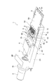
- FIG. 1 is a perspective view showing an optical device according to an embodiment.
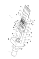
- FIG. 2 is a perspective view showing a state in which the cover is removed from the optical device of FIG.
- FIG. 3 is a diagram schematically showing the relationship between the base, the optical element, and the optical path of the optical device of the comparative example.
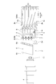
- FIG. 4 is a perspective view showing a lens, an optical component, a wiring board, and an optical element of the optical device of FIG.
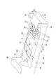
- FIG. 5 is a perspective view showing the base of the optical device of FIG.
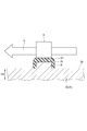
- FIG. 6 is a diagram schematically showing the relationship between the base, the optical element, and the optical path of the optical device of FIG.
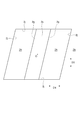
- FIG. 7 is a plan view showing the mounting surface and the groove portion of the base of FIG. FIG.
- FIG. 8 is a side sectional view showing a base, a lens, an optical component, a wiring board, and an optical element of the optical device of FIG.
- FIG. 9 is a plan view showing the base, the lens, the optical component, the wiring board, and the optical element of FIG.
- FIG. 10 is a perspective view showing a base according to the first modification.
- FIG. 11 is a perspective view showing a base according to the second modification.
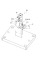
- FIG. 12 is a perspective view showing a jig for mounting a component on a base.
- FIG. 13 is a perspective view showing a state in which a component is fixed to the base using the jig of FIG.
- an optical device equipped with a non-hermetic type (non-airtight) storage body may be used for cost reduction.
- the optical device is an LD (Laser Diode), a carrier on which the LD is mounted, an FPC (Flexible Printed Circuit) having a pad electrically connected to the LD, and a monitor PD (Photo Diode) that monitors the light from the LD.
- LD Laser Diode
- FPC Flexible Printed Circuit
- monitor PD Photo Diode
- the base is equipped with a carrier, FPC and monitor PD.
- the base is L-shaped with a side wall to which the receptacle is mounted and a lower plate on which the carrier, FPC and monitor PD are mounted.
- optical components such as lenses may be mounted on the lower plate of the base.
- the optical element and the optical component are fixed to the upper surface of the lower plate with a resin adhesive. At this time, the adhesive under the optical element and the optical component may rise during bonding, and the adhesive may interfere with the optical path of the optical element and the optical component.
- the optical device is provided between an optical element, a lens that optically couples with the optical element, and optically couples with each of the optical element and the lens, and combines or combines input light. It comprises a demultiplexing optical component and a base having a lower plate with a plurality of convex mounting surfaces on which each of the optical elements, lenses and optical components is mounted, and a side wall to which the receptacle is connected.
- the base has a lower plate and a side wall, and the lower plate has a plurality of mounting surfaces.
- An optical element, a lens, and an optical component are mounted on each of the plurality of mounting surfaces.
- each of the plurality of mounting surfaces is convex. Therefore, if an adhesive is applied under each of the optical element, lens, and optical component and mounted on the convex mounting surface, even if the adhesive protrudes from the convex mounting surface, the protruding adhesive will be removed. It will flow downward from the mounting surface. Therefore, since it is possible to prevent the adhesive under the optical element, the lens, and the optical component from rising during bonding or the like, it is possible to suppress the interference of the adhesive with the optical path of the optical element, the lens, and the optical component. can.
- the heights of the plurality of mounting surfaces may be the same as each other.
- the plurality of convex mounting surfaces are formed by polishing
- the heights of the plurality of mounting surfaces are the same as each other, so that the polishability can be improved. That is, the mounting surfaces having the same height can be easily formed by polishing, and the dimensional accuracy of the mounting surfaces can be improved.
- the optical component may have two surfaces extending parallel to each other, and the mounting surface of the optical component may have two sides extending parallel to the two surfaces of the optical component.
- the distance between the two sides of the mounting surface of the optical component may be shorter than the distance between the two surfaces of the optical component. In this case, since the two surfaces of the optical component and the two sides of the mounting surface are arranged in parallel with each other, it is possible to eliminate the difference in the fanning angle that occurs in the optical component.
- Grooves may be provided on both sides in the longitudinal direction of the mounting surface of the base corresponding to the mounting surface of the optical component. In this case, even when the amount of the adhesive is large, the adhesive can escape to the groove, so that the interference of the adhesive with the optical path can be more reliably suppressed.
- the groove may have an outer wall along the outer shape of the optical component.
- the outer wall of the groove can be used for passive alignment of optical components.
- the method for manufacturing an optical device is provided between an optical element, a lens that optically couples with the optical element, and an optical element and a lens, and optically couples each of the optical element and the lens to emit input light. It comprises an optical component that is coupled or demultiplexed, and a base with a lower plate with multiple convex mounting surfaces on which each of the optical elements, lenses and optical components is mounted, and a side wall to which the receptacle connects.
- This is a method for manufacturing an optical device.
- grooves having an outer wall along the outer shape of the optical component are provided on both sides of the mounting surface of the base corresponding to the mounting surface of the optical component in the longitudinal direction, and the outer wall is used as an alignment marker to illuminate the mounting surface. It includes a process of mounting parts and a process of aligning the lens.
- each of the plurality of mounting surfaces is convex. Therefore, if an adhesive is applied under each of the optical element, lens, and optical component and mounted on the convex mounting surface, even if the adhesive protrudes from the convex mounting surface, the protruding adhesive will be removed. It will flow downward from the mounting surface. Therefore, since it is possible to suppress the adhesive under the optical element, the lens and the optical component from rising at the time of bonding or the like, it is possible to suppress the interference of the adhesive with the optical path of the optical element, the lens and the optical component.
- the lens can be aligned with the component mounted on the mounting surface using the outer wall of the groove as an alignment marker. Therefore, the optical components and the lens can be arranged on each mounting surface with high accuracy.
- FIG. 1 is a perspective view showing an optical device 1 according to the present embodiment.
- the optical device 1 which is an optical transmitter will be illustrated.
- the optical device 1 includes a base 2, a cover 3 covering the base 2, a receptacle 4 having a cylindrical sleeve, and a wiring board 5.
- the optical device 1 extends along the longitudinal direction D1, and the receptacle 4, the cover 3 (base 2), and the wiring board 5 are arranged in this order.
- FIG. 2 is a perspective view of the optical device 1 with the cover 3 removed.
- the base 2 includes a lower plate 2A extending in the longitudinal direction D1 and a side wall 2B extending in the height direction D2 from one end of the lower plate 2A in the longitudinal direction D1.
- the base 2 is made of metal, for example.
- the material of the base 2 is, for example, Kovar (an alloy in which at least nickel and cobalt are mixed with iron) or SUS (Steel Use Stainless).
- the base 2 may be composed of iron, chromium, an alloy of iron and chromium, an alloy of iron and nickel, or plastic.
- the shape of the base 2 seen from the width direction D3 of the optical device 1 is L-shaped.
- Base 2 is also called an L-shaped base.
- a receptacle 4 is connected to the side wall 2B and a hole which is an emission end of the output light L (see FIG. 3) is formed, and the hole penetrates the side wall 2B in the longitudinal direction D1.
- the receptacle 4 is formed in a cylindrical shape.
- the receptacle 4 has a plurality of flanges 4c, and one of the plurality of flanges 4c functions as a guide 4b for determining the position of the receptacle 4. In the receptacle 4, for example, the guide 4b comes into contact with the outer surface 2f of the side wall 2B in a state of being fixed to the base 2.
- the base 2 has a rectangular shape.
- the base 2 is a component for mounting a component housed inside the optical device 1, and each component of the optical device 1 is mounted on the lower plate 2A.
- the lower plate 2A is a long portion protruding from the side wall 2B in the longitudinal direction D1, and each component of the optical device 1 is mounted on the long portion.
- Each component of the optical device 1 is fixed to the lower plate 2A by the adhesive resin R (see FIG. 3).
- the lower plate 2A includes a main surface 2b facing each component inside the optical device 1, a guide pin 2d that determines the positions of the cover 3 and the wiring board 5 with respect to the base 2, and an outer surface 2f exposed to the outside of the optical device 1.
- the main surface 2b has a rectangular shape extending in the longitudinal direction D1 and the width direction D3.
- the guide pin 2d projects in the height direction D2 on the main surface 2b.
- the guide pin 2d is, for example, cylindrical.
- the guide pin 2d is provided, for example, on one side of the width direction D3 (a position deviated from the center of the width direction D3 of the base 2).
- the cover 3 is a component that covers the base 2 from the height direction D2.
- Each component of the optical device 1 is housed inside the base 2 and the cover 3.
- the optical device 1 Inside the base 2 and the cover 3, the optical device 1 includes a wiring substrate 5, an optical component 6, a light receiving element 7 (optical element), a first lens 8 (lens), a light emitting element 9 (optical element), a spacer 10, and a thermistor. 14 is provided. A part of the wiring board 5 extends from the base 2 and the cover 3 to the opposite side of the receptacle 4. The portion of the wiring board 5 extending to the opposite side of the receptacle 4 projects to the outside of the optical device 1.
- the optical device 1 further includes a second lens 11 interposed between the receptacle 4 and the optical component 6.
- the optical device 1 includes four light emitting elements 9, four first lenses 8, four light receiving elements 7, an optical component 6, and a second lens 11 (lens).
- the optical device 1 is a 4-lane multi-channel light emitting module including 4 light receiving elements 7, 4 first lenses 8 and 4 light receiving elements 7.
- the optical path length of the output light L is different from each other for each channel.
- the receptacle 4 is arranged, for example, at a position deviated from the center of the width direction D3 of the base 2.
- the optical path of the output light L from the light emitting element 9 located at the end opposite to the receptacle 4 in the width direction D3 (the upper end in FIG. 2) is the longest.
- the optical path of the output light L from the light emitting element 9 located at the end (lower end in FIG. 2) on the receptacle 4 side in the width direction D3 is the shortest.
- a plurality of light emitting elements 9 and a plurality of light receiving elements 7 are mounted on the base 2.
- the plurality of light emitting elements 9 are arranged so as to be arranged along the width direction D3, and the plurality of light receiving elements 7 are arranged so as to be arranged along the width direction D3.
- each of the four light emitting elements 9 is mounted on the main surface 2b of the base 2 via the carrier 12.
- Each light emitting element 9 is provided corresponding to each of the four first lenses 8 and each of the four light receiving elements 7.
- Each light emitting element 9 is, for example, a semiconductor laser diode (LD).
- the output light L which is the divergent light output from the light emitting element 9, is converted into collimated light by each first lens 8. In this way, the first lens 8 is optically coupled to the light emitting element 9.
- the wiring board 5 is, for example, an FPC (Flexible Printed Circuit) mounted on the base 2.
- the wiring board 5 includes a first region 5A extending outward from the optical device 1, a second region 5B provided with a pad 5b, and a connection region 5C connecting the first region 5A and the second region 5B to each other. ..
- the first region 5A, the second region 5B, and the connection region 5C are U-shaped (C-shaped) when viewed from the height direction D2.
- the first region 5A includes a pad 5d that is electrically connected to the light emitting element 9.
- each of the plurality of light emitting elements 9 is connected to the pad 5d via a wire.
- the first region 5A is provided at a position higher than the second region 5B (a position away from the main surface 2b of the base 2).
- the height position of the first region 5A coincides with the height of the carrier 12 on which the light emitting element 9 is mounted.
- the length of the wire extending from each light emitting element 9 to the pad 5d can be shortened.
- one wiring board 5 includes a first region 5A as an upper stage and a second region 5B as a lower stage, and is fixed to the base 2 by adhesion.
- the second region 5B is provided at a position lower than the first region 5A, and is in contact with, for example, the main surface 2b of the base 2. Since the position of the second region 5B is low, the wire extending from the wiring board 5 or the light receiving element 7 can be prevented from interfering with the output light L passing through the light emitting element 9 and the first lens 8.
- the width of the connection region 5C of the wiring board 5 (the length in the width direction D3) is narrower than the width of the first region 5A and the width of the second region 5B, respectively.
- the connection area 5C is provided, for example, at the end of the receptacle 4 side in the width direction D3.
- the connection region 5C extends from the end of the first region 5A in the width direction D3 to the end of the second region 5B in the width direction D3.
- the thickness of the wiring board 5 in the first region 5A and the thickness of the wiring board 5 in the second region 5B are, for example, the same as each other.
- connection region 5C extends in the longitudinal direction D1 between the first region 5A and the second region 5B and is located, for example, at the end of the base 2 in the width direction D3.
- the connection area 5C has a step or slope located between the first area 5A and the second area 5B. In this embodiment, an example is shown in which the connection region 5C has an inclination of 5f.
- the spacer 10 is provided between the first region 5A and the base 2, and for example, the height of the first region 5A is secured by the spacer 10.
- a reinforcing plate made of an insulating material may be provided in the first region 5A of the wiring board 5. In this case, it is possible to provide a wiring pattern on the lower surface of the first region 5A.
- the output light L output from the light emitting element 9 via the first lens 8 is input to the optical component 6 through the light receiving element 7.
- the optical component 6 is provided between the light emitting element 9 and the second lens 11, and the light emitting element 9 and the second lens 11 are optically coupled.
- the optical component 6 combines the input light (output light L) input to the optical component 6.
- the optical component 6 is an optical combiner that combines four output lights L.
- the four output lights L are output from the optical component 6 to the second lens 11 as one output light L that is combined inside the optical component 6.
- the second lens 11 condenses the output light L from the optical component 6 and condenses the output light L on the optical fiber held in the receptacle 4, and the output light L passes through the optical fiber held in the receptacle 4. Is output to the outside of the optical device 1.
- the second lens 11 is optically coupled to the light emitting element 9 via the optical component 6.
- the light receiving element 7 is a monitor PD (PhotoDiode) that monitors the output light L from each of the plurality of light emitting elements 9.
- the light receiving element 7 monitors the intensity of the output light L by receiving a part of the output light L from the light emitting element 9.
- each of the four light receiving elements 7 is mounted on the main surface 2b of the base 2 via a carrier made of a material containing a dielectric.
- the light receiving element 7 converts a part of the output light L from the light emitting element 9 into an electric signal, and outputs the converted electric signal to the pad 5b of the wiring board 5 via a wire (not shown).
- the light receiving element 7 and the wire extending from the light receiving element 7 to the pad 5b are provided on the light output side (receptacle 4 side) of the light emitting element 9.
- APC control AutoPowerControl
- the second region 5B is a PD wiring FPC having a pad 5b for wiring to the light receiving element 7, and is located on the optical output side (receptacle 4 side) of the light receiving element 7.
- the light receiving element 7 is a surface incident type light receiving element.
- the light receiving element 7 is arranged so that the light receiving surface thereof is inclined with respect to the optical axis of the output light L, for example. By arranging the light receiving element 7 so that the light receiving surface is slanted with respect to the optical axis of the output light L, the light receiving element 7 receives a part of the output light L.
- the light receiving element 7 on the light output side of the light emitting element 9, it is possible to monitor the output light L with a simple configuration on the light output side.
- Wiring such as a wire for the light receiving element 7 which is a monitor PD is provided on the optical output side of the light receiving element 7. Therefore, it is possible to make an electrical connection with the light receiving element 7 without lowering the light receiving sensitivity of the light receiving element 7. Since the light receiving element 7 is directly wired to the pad 5b on the wiring board 5, for example, it is not necessary to separately mount a carrier or the like. Therefore, it contributes to cost reduction.
- a component of the base 2 on which a component X inside the optical device 1 (for example, an optical component such as the optical component 6, the first lens 8 or the second lens 11 described above) is mounted.
- the mounting surface is a flat surface, the resin R for adhesion may protrude into the optical path of the output light L. In this way, there is a concern that the resin R that adheres the component X interferes with the optical path of the output light L.
- FIG. 4 is a perspective view showing the configuration of the base 2 capable of suppressing the interference of the resin R with the output light L.
- FIG. 5 is a perspective view showing the base 2 of FIG.
- the base 2 comprises a pair of upwardly projecting protrusions 2k at the opposite end of the longitudinal direction D1 to the side wall 2B.
- the pair of protrusions 2k are arranged so as to line up in the width direction D3.
- the first region 5A has a pair of recesses 5c arranged in the width direction D3.
- the wiring board 5 is fixed to the base 2 by fitting each protrusion 2k of the base 2 into each recess 5c.
- the base 2 has a convex mounting surface 2c on which components are mounted.
- the mounting surface 2c is an adhesive pedestal for parts.
- the mounting surface 2c is a surface on which each of the plurality of optical components of the optical device 1 is mounted.
- the base 2 includes a plurality of mounting surfaces 2c on the main surface 2b.
- Each of the plurality of mounting surfaces 2c mounts the optical component 6, the first lens 8, the second lens 11, and the carrier 12.
- the mounting surface 2c is a portion of the main surface 2b that projects in the height direction D2.
- Each mounting surface 2c is provided at a position higher than the main surface 2b.
- the plurality of mounting surfaces 2c have the same height as each other. In this case, when the plurality of mounting surfaces 2c are formed by polishing, the polishability can be improved and the dimensional accuracy can be improved.
- FIG. 6 is a side view schematically showing the component X, the mounting surface 2c, and the resin R of the optical device 1.
- the component X when the component X is mounted on the mounting surface 2c via the resin R, even if the resin R protrudes from the component X, the protruding resin R flows out below the mounting surface 2c. Therefore, it is possible to avoid the interference of the resin R with the output light L.
- the mounting surface 2c is contained in the component X.
- the mounting surface 2c is housed in a surface X1 (for example, a lower surface) facing the base 2 of the component X. This makes it possible to more reliably flow the resin R downward from the surface X1 of the component X mounted on the mounting surface 2c, and reduce the possibility that the resin R interferes with the output light L.
- FIG. 7 is a plan view showing a mounting surface 2c of an exemplary optical component 6.
- the optical component 6 has two surfaces 6b extending parallel to each other, and the mounting surface 2c on which the optical component 6 is mounted has two sides 2g extending parallel to the two surfaces 6b.
- a groove portion 2h lower than the main surface 2b is formed around the mounting surface 2c.
- the groove 2h is provided, for example, on one side and the other side of the mounting surface 2c in the longitudinal direction D1.
- the groove portion 2h has an outer wall 2j along the outer shape of the optical component 6.
- the outer wall 2j is a wall portion that constitutes the outer shape of the mounting surface 2c and the groove portion 2h when viewed from the height direction D2.
- the distance from the mounting surface 2c to the outer wall 2j on the end side in the longitudinal direction D1 is constant regardless of the position in the width direction D3. That is, the mounting surface 2c has a side 2g parallel to the surface 6b of the optical component 6, so that the above distance can be made constant.
- the mounting surface 2c and the outer wall 2j (optical component 6) have a shape that is point-symmetrical with respect to the center O when viewed from the height direction D2.
- the mounting surface 2c, the groove portion 2h, and the outer wall 2j have a parallel four-sided shape. Since the mounting surface 2c is a parallelogram, the deviation of the position (height from the main surface 2b of the base 2) of each incident surface of the surface 6b due to the tilt angle of the surface 6b of the optical component 6 is made constant. Is possible.
- the manufacturing method of the optical device according to this embodiment will be described.
- a method for manufacturing an exemplary optical device 1 will be described.
- the receptacle 4 and the base 2 are positioned.
- the receptacle 4 whose position has been adjusted with respect to the base 2 is fixed to the base 2 by YAG welding.
- a wiring board 5, a carrier 12 on which a light emitting element 9 is mounted, a light receiving element 7, a thermistor 14, and an optical component 6 are mounted.
- the optical component 6 is mounted on the mounting surface 2c with the outer wall 2j as an alignment marker (step of mounting the optical component).
- the outer wall 2j of the groove portion 2h has the shape of the optical component 6, so that passive alignment can be performed.
- the first lens 8 and the second lens 11 are mounted on each mounting surface 2c of the base 2. Then, the output light L is output from the mounted light emitting element 9 to align each of the first lens 8 and the second lens 11 (step of aligning the lens). After aligning each of the first lens 8 and the second lens 11 so as to maximize the intensity of the output light L, each of the first lens 8 and the second lens 11 is fixed (active alignment).
- the base 2 has a lower plate 2A and a side wall 2B, and the lower plate 2A includes a plurality of mounting surfaces 2c.
- a light emitting element 9 (carrier 12), a first lens 8, a second lens 11, and an optical component 6 are mounted on each of the plurality of mounting surfaces 2c.
- each of the plurality of mounting surfaces 2c is convex. Therefore, if the resin R is applied under each of the light emitting element 9, the first lens 8, the second lens 11, and the optical component 6 and mounted on the convex mounting surface 2c, even if the resin R protrudes, it may be mounted.
- the protruding resin R will flow downward from the mounting surface 2c. Therefore, it is possible to prevent the resin R under the light emitting element 9, the first lens 8, the second lens 11, and the optical component 6 from rising during bonding or the like. Therefore, it is possible to suppress the interference of the resin R with the optical path of the light emitting element 9, the first lens 8, the second lens 11, and the optical component 6.
- the adhesive region formed by the resin R has a convex shape, the adhesive region formed by the resin R can be controlled. For example, it is possible to suppress the deformation of the optical component 6 due to the difference in the coefficient of linear expansion when the external temperature changes.
- the heights of the plurality of mounting surfaces 2c may be the same as each other.
- the heights of the plurality of mounting surfaces 2c are the same as each other, so that the polishability can be improved. That is, the mounting surfaces 2c having the same height can be easily formed by polishing, and the dimensional accuracy of the mounting surfaces 2c can be improved. Further, since the dimensional tolerance can be reduced, the variation in the optical coupling efficiency can be suppressed.
- the optical component 6 may have two surfaces 6b extending parallel to each other, and the mounting surface 2c of the optical component 6 may have two sides 2g extending parallel to the two surfaces 6b of the optical component 6.
- the distance between the two sides 2g of the mounting surface 2c of the optical component 6 may be shorter than the distance between the two surfaces 6b of the optical component 6. In this case, since the two surfaces 6b of the optical component 6 and the two sides 2g of the mounting surface 2c are arranged in parallel with each other, it is possible to eliminate the difference in the fanning angle generated in the optical component 6.
- Grooves 2h may be provided on both sides of the mounting surface 2c of the base 2 corresponding to the mounting surface 2c of the optical component 6 in the longitudinal direction D1. In this case, even when the amount of the resin R is large, the resin R can escape to the groove 2h, so that the interference of the resin R with the optical path can be suppressed more reliably.
- the groove portion 2h may have an outer wall 2j along the outer shape of the optical component 6.
- the outer wall 2j of the groove portion 2h can be used for passive alignment of the optical component 6.
- each of the light emitting element 9, the first lens 8, the second lens 11 and the optical component 6 is mounted on each of the plurality of mounting surfaces 2c.
- Each of the first lens 8 and the second lens 11 can be aligned with the components mounted on the mounting surface 2c using the outer wall 2j of the groove portion 2h of the base 2 as an alignment marker. Therefore, the optical component 6, the first lens 8 and the second lens 11 can be arranged on the mounting surface 2c with high accuracy.
- Base 2 may be manufactured by MIM (Metal Injection Molding). In this case, the cost for manufacturing the base 2 can be suppressed.
- MIM Metal Injection Molding
- the base 2 since the side wall 2B to which the receptacle 4 is mounted and the lower plate 2A on which the parts are mounted are integrated, it is possible to reduce the component tolerance and to make the base 2 highly rigid. ..
- the base 2 includes a pair of projecting portions 2k projecting upward at an end opposite to the side wall 2B in the longitudinal direction D1. Therefore, for example, even if the base 2 on which the parts mounted as shown in FIG. 4 is erroneously arranged upside down, the side wall 2B and the protruding portion 2k hit the floor or the like, so that the mounted parts do not interfere with the floor or the like. can.
- the base 22 includes a convex mounting surface 2c on which components are mounted, as well as a convex portion 22c for fixing a component mounting jig.
- the convex portion 22c and the mounting surface 2c are arranged so as to be arranged along the width direction D3, for example.
- the position of the convex portion 22c in the longitudinal direction D1 is the same as the position of the mounting surface 2c in the longitudinal direction D1.
- the height of the convex portion 22c is the same as the height of the mounting surface 2c.
- the base 32 has a convex portion 32c having a planar shape longer in the width direction D3 than the planar shape (shape seen from the height direction D2) of the component (for example, the second lens 11). Be prepared.
- the convex portion 32c has a contact portion to which a component mounting jig is applied when the component is mounted.
- the component mounting jig 40 is a jig for positioning the sleeve 4A of the receptacle 4 and the base 2.
- the component mounting jig 40 includes a base holding portion 41 for holding the base 2 and a sleeve holding portion 42 for holding the sleeve 4A.
- the base holding portion 41 has a facing portion 41b facing the main surface 2b side of the lower plate 2A of the base 2, and a holding portion 41c holding the base 2 with the lower plate 2A facing the facing portion 41b.
- the sleeve 4A with respect to the base 22 or the base 32 in a state where the convex portion 22c or the convex portion 32c is abutted against the contact surface 41d of the facing portion 41b. Can be positioned. Therefore, since the sleeve 4A can be positioned with the base 22 or the base 32 stabilized, the positioning accuracy of the sleeve 4A with respect to the parts mounted on the base 22 or the base 32 can be improved. As a result, the alignment tolerance of the optical component can be increased, and the manufacturability can be improved.
- the sleeve 4A whose position has been adjusted with respect to the base 22 or the base 32 is fixed to the base 22 or the base 32 by YAG welding.
- the present invention is not limited to the above-described embodiment. That is, it is easily recognized by those skilled in the art that the present invention can be modified and modified in various ways without changing the gist described in the claims.
- the shape, size, number, material, and arrangement mode of each component of the optical device are not limited to the above-mentioned contents and can be appropriately changed.
- the optical device 1 which is an optical transmitter
- the optical device according to the present disclosure may be an optical device other than the optical transmitter, and may be, for example, an optical receiver.
- the optical component 6 which is an optical combiner is exemplified.
- the optical component may be an optical component other than the optical combiner, and may be, for example, an optical duplexer that demultiplexes the input light. In this way, the type of the optical device and the parts mounted on the optical device can be changed as appropriate.
- Light emitting element (optical element) 10 Spacer 11 ... Second lens (lens) 12 ... Carrier 14 ... Thermistor 22c, 32c ... Convex part 40 ... Parts mounting jig 41 ... Base holding part 41b ... Opposing part 41c ... Holding part 41d ... Contact surface 42 ... Sleeve holding part D1 ... Longitudinal direction D2 ... Height Direction D3 ... Width direction L ... Output light O ... Center R ... Resin (adhesive) X ... Parts X1 ... Surface
Landscapes
- Physics & Mathematics (AREA)
- General Physics & Mathematics (AREA)
- Optics & Photonics (AREA)
- Condensed Matter Physics & Semiconductors (AREA)
- Electromagnetism (AREA)
- Optical Couplings Of Light Guides (AREA)
- Semiconductor Lasers (AREA)
Priority Applications (3)
| Application Number | Priority Date | Filing Date | Title |
|---|---|---|---|
| JP2022530636A JP7569857B2 (ja) | 2020-06-12 | 2021-06-11 | 光装置、および光装置の製造方法 |
| US18/009,247 US12429657B2 (en) | 2020-06-12 | 2021-06-11 | Optical device and manufacturing method for optical device |
| CN202180040764.1A CN115698802B (zh) | 2020-06-12 | 2021-06-11 | 光装置以及光装置的制造方法 |
Applications Claiming Priority (2)
| Application Number | Priority Date | Filing Date | Title |
|---|---|---|---|
| JP2020102422 | 2020-06-12 | ||
| JP2020-102422 | 2020-06-12 |
Publications (1)
| Publication Number | Publication Date |
|---|---|
| WO2021251488A1 true WO2021251488A1 (ja) | 2021-12-16 |
Family
ID=78846140
Family Applications (1)
| Application Number | Title | Priority Date | Filing Date |
|---|---|---|---|
| PCT/JP2021/022326 Ceased WO2021251488A1 (ja) | 2020-06-12 | 2021-06-11 | 光装置、および光装置の製造方法 |
Country Status (5)
| Country | Link |
|---|---|
| US (1) | US12429657B2 (https=) |
| JP (1) | JP7569857B2 (https=) |
| CN (1) | CN115698802B (https=) |
| TW (1) | TWI891815B (https=) |
| WO (1) | WO2021251488A1 (https=) |
Families Citing this family (1)
| Publication number | Priority date | Publication date | Assignee | Title |
|---|---|---|---|---|
| CN115836238A (zh) * | 2020-06-12 | 2023-03-21 | 住友电工光电子器件创新株式会社 | 光装置、基座以及基座的制造方法 |
Citations (4)
| Publication number | Priority date | Publication date | Assignee | Title |
|---|---|---|---|---|
| JP2014095843A (ja) * | 2012-11-12 | 2014-05-22 | Sumitomo Electric Ind Ltd | 光合分波器およびその製造方法ならびに光通信モジュール |
| JP2014102498A (ja) * | 2012-10-26 | 2014-06-05 | Sumitomo Electric Ind Ltd | 波長多重光送信モジュール及びその製造方法 |
| US20140263970A1 (en) * | 2013-03-14 | 2014-09-18 | Mark HEIMBUCH | Actively Aligned Detectors for Optical and Optoelectronic Arrays |
| WO2020004872A1 (en) * | 2018-06-28 | 2020-01-02 | Opticis Co., Ltd. | Optical connector |
Family Cites Families (8)
| Publication number | Priority date | Publication date | Assignee | Title |
|---|---|---|---|---|
| JP2004061541A (ja) * | 2002-07-24 | 2004-02-26 | Sumitomo Electric Ind Ltd | 光モジュール |
| JP2005033037A (ja) | 2003-07-07 | 2005-02-03 | Sumitomo Electric Ind Ltd | 半導体発光モジュール |
| JP2013101244A (ja) | 2011-11-09 | 2013-05-23 | Furukawa Electric Co Ltd:The | 光モジュール |
| CN103959124A (zh) | 2012-10-26 | 2014-07-30 | 住友电气工业株式会社 | 波分复用发射器光学模块 |
| CN105474062B (zh) * | 2014-06-10 | 2017-06-30 | 住友电气工业株式会社 | 光接收器组件及组装光接收器组件的方法 |
| US10128974B2 (en) | 2014-06-12 | 2018-11-13 | Sumitomo Electric Industries, Ltd. | Optical receiver module and process to assemble optical receiver module |
| US10386579B2 (en) * | 2014-10-31 | 2019-08-20 | Sumitomo Electric Industries, Ltd. | Optical transmitting module and multi-lane transmitter optical module |
| JP6380069B2 (ja) * | 2014-12-11 | 2018-08-29 | 住友電気工業株式会社 | 光送信モジュール |
-
2021
- 2021-06-11 CN CN202180040764.1A patent/CN115698802B/zh active Active
- 2021-06-11 US US18/009,247 patent/US12429657B2/en active Active
- 2021-06-11 WO PCT/JP2021/022326 patent/WO2021251488A1/ja not_active Ceased
- 2021-06-11 JP JP2022530636A patent/JP7569857B2/ja active Active
- 2021-06-11 TW TW110121408A patent/TWI891815B/zh active
Patent Citations (4)
| Publication number | Priority date | Publication date | Assignee | Title |
|---|---|---|---|---|
| JP2014102498A (ja) * | 2012-10-26 | 2014-06-05 | Sumitomo Electric Ind Ltd | 波長多重光送信モジュール及びその製造方法 |
| JP2014095843A (ja) * | 2012-11-12 | 2014-05-22 | Sumitomo Electric Ind Ltd | 光合分波器およびその製造方法ならびに光通信モジュール |
| US20140263970A1 (en) * | 2013-03-14 | 2014-09-18 | Mark HEIMBUCH | Actively Aligned Detectors for Optical and Optoelectronic Arrays |
| WO2020004872A1 (en) * | 2018-06-28 | 2020-01-02 | Opticis Co., Ltd. | Optical connector |
Also Published As
| Publication number | Publication date |
|---|---|
| TW202203533A (zh) | 2022-01-16 |
| JP7569857B2 (ja) | 2024-10-18 |
| CN115698802B (zh) | 2026-03-31 |
| TWI891815B (zh) | 2025-08-01 |
| CN115698802A (zh) | 2023-02-03 |
| US12429657B2 (en) | 2025-09-30 |
| JPWO2021251488A1 (https=) | 2021-12-16 |
| US20230221505A1 (en) | 2023-07-13 |
Similar Documents
| Publication | Publication Date | Title |
|---|---|---|
| EP2428828B1 (en) | Miniaturized high speed optical module | |
| US7108432B2 (en) | Connection structure for optical device, optical device and electronic device | |
| KR100844068B1 (ko) | 광전송 모듈 및 그 제조방법 | |
| US8475057B2 (en) | Optical module with ceramic package | |
| US11901946B2 (en) | Optical transmitter | |
| US6101202A (en) | Semiconductor laser module | |
| WO2010131767A2 (en) | Optical subassembly with optical device having ceramic pacakge | |
| JP2008203427A (ja) | 光モジュール | |
| US8475058B2 (en) | Optical module with ceramic package reducing optical coupling stress | |
| KR20180031262A (ko) | 다채널 광 서브 어셈블리 및 그의 제조방법 | |
| JP4269291B2 (ja) | 光モジュール | |
| WO2021251488A1 (ja) | 光装置、および光装置の製造方法 | |
| US20190250342A1 (en) | Optical module and method of manufacturing optical module | |
| JP7737985B2 (ja) | 光送信器 | |
| JP2007178537A (ja) | 光モジュールおよび光伝送システム | |
| WO2021251489A1 (ja) | 光装置、ベース、およびベースの製造方法 | |
| JPH04221912A (ja) | 並列伝送光モジュール | |
| TWI915377B (zh) | 光裝置、基座、及基座之製造方法 | |
| JP2021086050A (ja) | 光導波路モジュール | |
| CN120686416A (zh) | 光模块 |
Legal Events
| Date | Code | Title | Description |
|---|---|---|---|
| 121 | Ep: the epo has been informed by wipo that ep was designated in this application |
Ref document number: 21821632 Country of ref document: EP Kind code of ref document: A1 |
|
| ENP | Entry into the national phase |
Ref document number: 2022530636 Country of ref document: JP Kind code of ref document: A |
|
| NENP | Non-entry into the national phase |
Ref country code: DE |
|
| 122 | Ep: pct application non-entry in european phase |
Ref document number: 21821632 Country of ref document: EP Kind code of ref document: A1 |
|
| WWG | Wipo information: grant in national office |
Ref document number: 18009247 Country of ref document: US |