WO2021235227A1 - パターン測定方法 - Google Patents
パターン測定方法 Download PDFInfo
- Publication number
- WO2021235227A1 WO2021235227A1 PCT/JP2021/017356 JP2021017356W WO2021235227A1 WO 2021235227 A1 WO2021235227 A1 WO 2021235227A1 JP 2021017356 W JP2021017356 W JP 2021017356W WO 2021235227 A1 WO2021235227 A1 WO 2021235227A1
- Authority
- WO
- WIPO (PCT)
- Prior art keywords
- pattern
- cad
- edge
- measurement
- actual
- Prior art date
- Legal status (The legal status is an assumption and is not a legal conclusion. Google has not performed a legal analysis and makes no representation as to the accuracy of the status listed.)
- Ceased
Links
Images


Classifications
-
- G—PHYSICS
- G06—COMPUTING OR CALCULATING; COUNTING
- G06T—IMAGE DATA PROCESSING OR GENERATION, IN GENERAL
- G06T7/00—Image analysis
- G06T7/0002—Inspection of images, e.g. flaw detection
- G06T7/0004—Industrial image inspection
- G06T7/001—Industrial image inspection using an image reference approach
-
- H—ELECTRICITY
- H01—ELECTRIC ELEMENTS
- H01L—SEMICONDUCTOR DEVICES NOT COVERED BY CLASS H10
- H01L22/00—Testing or measuring during manufacture or treatment; Reliability measurements, i.e. testing of parts without further processing to modify the parts as such; Structural arrangements therefor
- H01L22/10—Measuring as part of the manufacturing process
- H01L22/12—Measuring as part of the manufacturing process for structural parameters, e.g. thickness, line width, refractive index, temperature, warp, bond strength, defects, optical inspection, electrical measurement of structural dimensions, metallurgic measurement of diffusions
-
- G—PHYSICS
- G06—COMPUTING OR CALCULATING; COUNTING
- G06T—IMAGE DATA PROCESSING OR GENERATION, IN GENERAL
- G06T7/00—Image analysis
- G06T7/10—Segmentation; Edge detection
- G06T7/13—Edge detection
-
- G—PHYSICS
- G06—COMPUTING OR CALCULATING; COUNTING
- G06T—IMAGE DATA PROCESSING OR GENERATION, IN GENERAL
- G06T7/00—Image analysis
- G06T7/30—Determination of transform parameters for the alignment of images, i.e. image registration
- G06T7/33—Determination of transform parameters for the alignment of images, i.e. image registration using feature-based methods
- G06T7/337—Determination of transform parameters for the alignment of images, i.e. image registration using feature-based methods involving reference images or patches
-
- G—PHYSICS
- G06—COMPUTING OR CALCULATING; COUNTING
- G06T—IMAGE DATA PROCESSING OR GENERATION, IN GENERAL
- G06T7/00—Image analysis
- G06T7/60—Analysis of geometric attributes
-
- G—PHYSICS
- G06—COMPUTING OR CALCULATING; COUNTING
- G06T—IMAGE DATA PROCESSING OR GENERATION, IN GENERAL
- G06T7/00—Image analysis
- G06T7/60—Analysis of geometric attributes
- G06T7/62—Analysis of geometric attributes of area, perimeter, diameter or volume
-
- G—PHYSICS
- G06—COMPUTING OR CALCULATING; COUNTING
- G06T—IMAGE DATA PROCESSING OR GENERATION, IN GENERAL
- G06T7/00—Image analysis
- G06T7/70—Determining position or orientation of objects or cameras
-
- H—ELECTRICITY
- H01—ELECTRIC ELEMENTS
- H01L—SEMICONDUCTOR DEVICES NOT COVERED BY CLASS H10
- H01L22/00—Testing or measuring during manufacture or treatment; Reliability measurements, i.e. testing of parts without further processing to modify the parts as such; Structural arrangements therefor
-
- H—ELECTRICITY
- H01—ELECTRIC ELEMENTS
- H01L—SEMICONDUCTOR DEVICES NOT COVERED BY CLASS H10
- H01L22/00—Testing or measuring during manufacture or treatment; Reliability measurements, i.e. testing of parts without further processing to modify the parts as such; Structural arrangements therefor
- H01L22/20—Sequence of activities consisting of a plurality of measurements, corrections, marking or sorting steps
-
- G—PHYSICS
- G01—MEASURING; TESTING
- G01N—INVESTIGATING OR ANALYSING MATERIALS BY DETERMINING THEIR CHEMICAL OR PHYSICAL PROPERTIES
- G01N2223/00—Investigating materials by wave or particle radiation
- G01N2223/40—Imaging
- G01N2223/421—Imaging digitised image, analysed in real time (recognition algorithms)
-
- G—PHYSICS
- G01—MEASURING; TESTING
- G01N—INVESTIGATING OR ANALYSING MATERIALS BY DETERMINING THEIR CHEMICAL OR PHYSICAL PROPERTIES
- G01N2223/00—Investigating materials by wave or particle radiation
- G01N2223/60—Specific applications or type of materials
- G01N2223/611—Specific applications or type of materials patterned objects; electronic devices
-
- G—PHYSICS
- G01—MEASURING; TESTING
- G01N—INVESTIGATING OR ANALYSING MATERIALS BY DETERMINING THEIR CHEMICAL OR PHYSICAL PROPERTIES
- G01N23/00—Investigating or analysing materials by the use of wave or particle radiation, e.g. X-rays or neutrons, not covered by groups G01N3/00 – G01N17/00, G01N21/00 or G01N22/00
- G01N23/22—Investigating or analysing materials by the use of wave or particle radiation, e.g. X-rays or neutrons, not covered by groups G01N3/00 – G01N17/00, G01N21/00 or G01N22/00 by measuring secondary emission from the material
- G01N23/225—Investigating or analysing materials by the use of wave or particle radiation, e.g. X-rays or neutrons, not covered by groups G01N3/00 – G01N17/00, G01N21/00 or G01N22/00 by measuring secondary emission from the material using electron or ion
- G01N23/2251—Investigating or analysing materials by the use of wave or particle radiation, e.g. X-rays or neutrons, not covered by groups G01N3/00 – G01N17/00, G01N21/00 or G01N22/00 by measuring secondary emission from the material using electron or ion using incident electron beams, e.g. scanning electron microscopy [SEM]
-
- G—PHYSICS
- G06—COMPUTING OR CALCULATING; COUNTING
- G06T—IMAGE DATA PROCESSING OR GENERATION, IN GENERAL
- G06T2207/00—Indexing scheme for image analysis or image enhancement
- G06T2207/10—Image acquisition modality
- G06T2207/10056—Microscopic image
- G06T2207/10061—Microscopic image from scanning electron microscope
-
- G—PHYSICS
- G06—COMPUTING OR CALCULATING; COUNTING
- G06T—IMAGE DATA PROCESSING OR GENERATION, IN GENERAL
- G06T2207/00—Indexing scheme for image analysis or image enhancement
- G06T2207/30—Subject of image; Context of image processing
- G06T2207/30108—Industrial image inspection
- G06T2207/30148—Semiconductor; IC; Wafer
-
- G—PHYSICS
- G06—COMPUTING OR CALCULATING; COUNTING
- G06T—IMAGE DATA PROCESSING OR GENERATION, IN GENERAL
- G06T2207/00—Indexing scheme for image analysis or image enhancement
- G06T2207/30—Subject of image; Context of image processing
- G06T2207/30108—Industrial image inspection
- G06T2207/30164—Workpiece; Machine component
Definitions
- the present invention relates to a method for measuring a feature quantity such as a pattern dimension (Critical Dimension) on an image generated by an image generator such as a scanning electron microscope, and particularly for workpieces such as wafers, masks, panels, and substrates. It relates to a method of automatically determining a measurement recipe of a feature amount such as a dimension of a formed pattern.
- a feature quantity such as a pattern dimension (Critical Dimension) on an image generated by an image generator such as a scanning electron microscope, and particularly for workpieces such as wafers, masks, panels, and substrates. It relates to a method of automatically determining a measurement recipe of a feature amount such as a dimension of a formed pattern.
- Patterns formed on workpieces such as wafers, masks, panels, and substrates usually have edges of various shapes such as straight edges and corner edges.
- the pattern is formed on the surface of the workpiece according to the design data (also referred to as CAD data).
- CAD data also referred to as CAD data.
- CD Cross Dimension
- an image of a pattern formed on a workpiece is generated by a scanning electron microscope, and the dimension of the pattern on the image is measured.
- Measurements are measured at many measurement points where pattern defects are likely to occur. These measurement points are specified on the coordinate system defined in the design data. In such dimensional measurement, a measurement recipe suitable for the pattern to be measured is manually set for each measurement point.
- the present invention provides a pattern measurement method capable of automatically determining a recipe for measuring a feature amount such as a pattern width dimension.
- the CAD pattern type and measurement recipe are determined based on the relative position between the measurement point on the coordinate system defined in the design data and the CAD pattern, and the area of the CAD pattern, and the CAD pattern is used.
- the type of CAD pattern is one selected from a plurality of types including at least an isolated pattern, a linear pattern, a curved pattern, and a terminal pattern.
- the measurement recipe includes at least measuring the width of the real pattern on the image, measuring the distance between the real patterns on the image, and measuring the misalignment of the edges of the real pattern on the image. It is one selected from multiple measurement recipes.
- the CAD pattern when the area of the CAD pattern is smaller than the predetermined area, the CAD pattern is determined to be an isolated pattern. In one aspect, the first edge of the CAD pattern closest to the measurement point and the second edge beyond the measurement point on the opposite side of the first edge have vertices in a predetermined search area. If not, the CAD pattern is determined to be a linear pattern. In one aspect, the CAD pattern is determined to be a curved pattern when at least one of the first edge and the second edge has vertices in the predetermined search area. In one aspect, when the edge length of the CAD pattern closest to the measurement point is shorter than a predetermined length and the area of the CAD pattern is larger than a predetermined area, the CAD pattern is a terminal pattern. Is determined to be.
- the type of CAD pattern can be determined and the optimum measurement recipe can be determined based on the relative position between the measurement point and the CAD pattern on the design data and the area of the CAD pattern.
- FIG. 5A is a schematic diagram showing an embodiment for measuring the distance between isolated patterns.
- FIG. 5B is a schematic diagram showing an embodiment for measuring the distance between isolated patterns. It is a schematic diagram explaining one Embodiment which measures the width of a linear pattern. It is a schematic diagram explaining one embodiment which measures the distance between linear patterns.
- FIG. 1 is a schematic diagram showing an embodiment of an image generation system.
- the image generation system includes a scanning electron microscope 1 that generates an image of the workpiece W, and an operation control unit 5 that controls the operation of the scanning electron microscope 1.
- Examples of the workpiece W include wafers, masks, panels, substrates and the like used in the manufacture of semiconductor devices.
- the operation control unit 5 is composed of at least one computer.
- the operation control unit 5 includes a storage device 5a in which the program is stored, and a processing device 5b that executes an operation according to an instruction included in the program.
- the storage device 5a includes a main storage device such as a random access memory (RAM) and an auxiliary storage device such as a hard disk drive (HDD) and a solid state drive (SSD).
- Examples of the processing device 5b include a CPU (central processing unit) and a GPU (graphic processing unit).
- the specific configuration of the motion control unit 5 is not limited to these examples.
- the scanning electron microscope 1 includes an electron gun 15 that emits an electron beam, a focusing lens 16 that focuses the electron beam emitted from the electron gun 15, an X deflector 17 that deflects the electron beam in the X direction, and an electron beam in the Y direction. It has a Y deflector 18 that deflects, an objective lens 20 that focuses an electron beam on a workpiece W that is an example of a sample, and a stage 31 that supports the workpiece W.
- the electron beam emitted from the electron gun 15 is focused by the focusing lens 16, then focused by the objective lens 20 while being deflected by the X deflector 17 and the Y deflector 18, and is irradiated on the surface of the workpiece W.
- electrons such as secondary electrons and backscattered electrons are emitted from the workpiece W.
- the electrons emitted from the workpiece W are detected by the electron detector 26.
- the electron detection signal of the electron detector 26 is input to the image acquisition device 28 and converted into an image. In this way, the scanning electron microscope 1 produces an image of the surface of the workpiece W.
- the image acquisition device 28 is connected to the motion control unit 5, and the image of the workpiece W is sent to the motion control unit 5.
- the pattern on the workpiece W is formed based on the design data (also referred to as CAD data).
- CAD is an abbreviation for computer-aided design.
- examples of the features of the actual pattern on the image are the width dimension of the actual pattern, the distance between the actual patterns, the positional deviation of the edges of the actual pattern, the positional deviation of the entire actual pattern, and the actual pattern. Examples include the area of the actual pattern (particularly the isolated pattern), the flatness of the actual pattern (particularly the isolated pattern), the line edge roughness of the actual pattern (particularly the linear pattern or the curved pattern), and the curvature of the actual pattern (particularly the curved pattern).
- the design data of the pattern formed on the workpiece W is stored in advance in the storage device 5a.
- the design data includes pattern design information such as the coordinates of the vertices of the pattern formed on the workpiece W, the position, shape, and size of the pattern, and the number of the layer to which the pattern belongs.
- the operation control unit 5 can read the pattern design data from the storage device 5a.
- the design data is data including design information of the pattern formed on the workpiece W.
- the CAD pattern on the design data described below is a virtual pattern defined by the design information of the pattern included in the design data, and has a polygon shape.
- the pattern actually formed on the workpiece W may be referred to as an actual pattern.
- the measurement point for specifying the measurement position of the feature amount of the pattern on the image is input to the operation control unit 5 and stored in the storage device 5a.
- the measurement point is a point where defects in the pattern formed on the workpiece W are likely to occur. For example, if the width dimension (CD or Critical Dimension) of the pattern at the measurement point is too long or too short, the motion control unit 5 can determine that the pattern is defective.
- the position of the measurement point is specified by the coordinates (X coordinate, Y coordinate) representing the points on the coordinate system defined in the design data.
- the position, shape, and size of the CAD pattern on the design data can also be specified by the vertices of the CAD pattern on the coordinate system. Usually, a large number of measurement points are set on the coordinate system.
- the motion control unit 5 is configured to determine the type of CAD pattern and the measurement recipe based on the relative position between the measurement point and the CAD pattern on the coordinate system defined in the design data and the area of the CAD pattern.
- Types of CAD patterns include at least isolated patterns, linear patterns, curved patterns, and termination patterns.
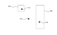
- FIG. 2 is a schematic diagram showing an example of measurement points and CAD patterns on the coordinate system defined in the design data.
- the CAD pattern 101 is a hole pattern which is an example of an isolated pattern, and the CAD pattern 102 is a linear pattern.
- three measurement points 111, 112, and 113 are set and plotted on the coordinate system.
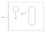
- FIG. 3 is a schematic diagram showing images 130 of actual patterns 121 and 122 on the workpiece W corresponding to CAD patterns 101 and 102.
- the corresponding actual patterns 121 and 122 are patterns actually formed on the workpiece W according to the CAD patterns 101 and 102.
- the images 130 of the actual patterns 121 and 122 are transmitted to the motion control unit 5.
- the motion control unit 5 aligns the CAD patterns 101 and 102 with the corresponding actual patterns 121 and 122 on the image 130 of the workpiece W. By aligning, it is possible to correct the positional deviation that occurs when the image is generated, and to measure the feature amount at the accurate position specified by the coordinates of the measurement point.
- a known pattern matching technique can be used for aligning the actual patterns 121 and 122 on the image 130 with the CAD patterns 101 and 102.
- the motion control unit 5 determines the type of CAD pattern and the measurement recipe based on the relative position between the measurement point on the coordinate system and the CAD pattern, and the area of the CAD pattern, and the actual pattern on the image is determined according to the determined measurement recipe. Perform the measurement of the feature quantity of.
- a method for determining a CAD pattern type and a measurement recipe will be described.
- the motion control unit 5 first determines whether or not the given measurement points 111, 112, 113 are inside the CAD patterns 101, 102 on the design data.
- the measurement points 111 and 113 are located inside the CAD patterns 101 and 102, respectively, and the measurement points 112 are located outside the CAD patterns 101 and 102.
- the motion control unit 5 calculates the area of the CAD patterns 101 and 102. When the area of the CAD pattern is smaller than the predetermined area, the motion control unit 5 determines that the CAD pattern is an isolated pattern. In the example shown in FIG. 2, the area of the CAD pattern 101 is smaller than the predetermined area, and therefore the motion control unit 5 determines that the CAD pattern 101 is an isolated pattern. On the other hand, the area of the CAD pattern 102 is larger than the predetermined area, and therefore the motion control unit 5 determines that the CAD pattern 102 is not an isolated pattern.
- the motion control unit 5 measures the width of the actual pattern corresponding to the CAD pattern 101 determined to be the isolated pattern. Specifically, the width dimension (Critical Dimension) of the actual pattern 121 (corresponding to the CAD pattern 101 of FIG. 2) on the screen 130 shown in FIG. 3 is measured. In one embodiment, the motion control unit 5 may further calculate the area and / or the flatness of the actual pattern 121 as the feature amount of the pattern. Further, in one embodiment, the motion control unit 5 may measure the position deviation of the entire actual pattern 121, that is, the deviation amount between the actual pattern 121 and the corresponding CAD pattern 101 as the feature amount of the pattern. ..
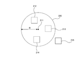
- 5A and 5B are schematic views showing an embodiment in which the distance between isolated patterns is measured as a feature amount.
- the motion control unit 5 when the measurement point 211 is outside the CAD pattern 212, 213, 214, 215, the motion control unit 5 is within a circular region 220 having a predetermined radius R centered on the measurement point 211.
- the CAD patterns 212, 213, 214 to be located are determined.
- the motion control unit 5 calculates the areas of the CAD patterns 212, 213, and 214 in the area 220, respectively.
- the measurement point 211 is located between the CAD patterns 212 and 213, between the CAD patterns 213 and 214, and further between the CAD patterns 214 and 212.
- the motion control unit 5 determines the CAD patterns 212, 213, 214 as the CAD patterns for which the distance between the isolated patterns is to be measured. do.
- the motion control unit 5 obtains the center-of-gravity positions G1, G2, and G3 of the CAD patterns 212, 213, and 214, and further on a line segment connecting the center-of-gravity positions G1, G2, and G3. Find the midpoint 222,223,224.
- the motion control unit 5 measures the distances L1, L2, and L3 from the measurement point 211 to the midpoint 222,223,224.
- the motion control unit 5 measures the distance between the actual patterns on the image corresponding to the CAD pattern located at both ends of the line segment including the midpoint. ..
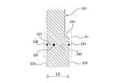
- FIG. 6 is a schematic diagram illustrating an embodiment in which the width of a linear pattern is measured as a feature amount.
- the motion control unit 5 determines that the CAD pattern 231 is not an isolated pattern.
- the motion control unit 5 determines the first edge 233 of the CAD pattern 231 on the design data closest to the measurement point 232. Further, the motion control unit 5 determines the second edge 234 which is on the opposite side of the first edge 233 beyond the measurement point 232.
- the second edge 234 is parallel to the first edge 233.
- the measurement point 232 is located between the first edge 233 and the second edge 234.
- Part 5 determines that the CAD pattern 231 is a linear pattern.
- the search region T1 extends from the measurement point 232 and surrounds the first vertical line 237 perpendicular to the first edge 233 and the first intersection 238 with the first edge 233, and further extends from the measurement point 232 to the second edge 234. It is a region surrounding the second intersection 241 of the vertical second vertical line 240 and the second edge 234.
- the size of the search area T1 can be set as a parameter.
- the motion control unit 5 determines that the measurement point 232 is in the CAD pattern 231 and further measures the width dimension (Critical Dimension) of the actual pattern on the image corresponding to the CAD pattern 231 which is a linear pattern. In one embodiment, the motion control unit 5 may further calculate the line edge roughness of the actual pattern as the feature amount of the pattern. Further, in one embodiment, the motion control unit 5 may measure the position deviation of the entire actual pattern, that is, the deviation amount between the actual pattern and the corresponding CAD pattern 231 as the feature amount of the pattern.
- the motion control unit 5 is configured to ignore steps smaller than a predetermined size when determining the presence or absence of edge vertices. Therefore, if there is a small step on the edge, the CAD pattern is determined to be a linear pattern.
- FIG. 7 is a schematic diagram illustrating an embodiment in which the distance between linear patterns is measured as a feature amount. Since the operation of the present embodiment, which is not particularly described, is the same as that of the embodiment described with reference to FIG. 6, the duplicated description thereof will be omitted.
- the motion control unit 5 determines that the measurement point 232 is located outside the CAD patterns 231 and 245 on the design data and is located between the CAD patterns 231 and 245. Further, the distance between the actual patterns on the image corresponding to the CAD patterns 231 and 245 is measured.
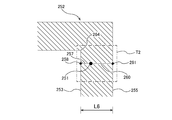
- FIG. 8 is a schematic diagram illustrating an embodiment in which the width of a curved pattern is measured as a feature amount.
- the motion control unit 5 determines the first edge 253 of the CAD pattern 252 on the design data closest to the measurement point 251.
- the motion control unit 5 determines the second edge 255 that is on the opposite side of the first edge 253 beyond the measurement point 251.
- the second edge 255 is parallel to the first edge 253.
- the measurement point 251 is located between the first edge 253 and the second edge 255.
- the distance L6 between the first edge 253 and the second edge 255 is shorter than the threshold value, and at least one of the first edge 253 and the second edge 255 has a vertex in the predetermined search area T2.
- the motion control unit 5 determines that the CAD pattern 252 is a curved pattern.
- the search region T2 extends from the measurement point 251 and surrounds the first vertical line 257 perpendicular to the first edge 253 and the first intersection 258 with the first edge 253, and further extends from the measurement point 251 to the second edge 255. It is a region surrounding the second intersection 261 of the vertical second perpendicular line 260 and the second edge 255.
- the size of the search area T2 can be set as a parameter. In the embodiment shown in FIG. 8, since the first edge 253 has the apex 264 in the search region T2, the motion control unit 5 determines that the CAD pattern 252 is a curved pattern.
- FIG. 9 is a schematic diagram illustrating an embodiment of a method of determining a measurement point and a measurement direction of a curve pattern.
- the actual pattern formed on a workpiece such as a wafer has rounded corner edges due to processes such as exposure and etching.
- the CAD pattern 252 is subjected to a rounding process as shown by reference numerals 267 and 268 in FIG. An arc, a Bezier curve, or the like is used for this rounding process.
- the motion control unit 5 determines the shortest point 270, which has the shortest distance from the measurement point 251 to the curve 267.
- the motion control unit 5 draws the normal line 271 of the curve 267 from the shortest point 270, and determines the intersection 275 between the opposite curve 268 and the normal line 271.
- the motion control unit 5 measures the width of the actual pattern in the extending direction of the normal 271.
- the motion control unit 5 may further calculate the curvature and / or the line edge roughness of the actual pattern as the feature amount of the pattern.
- FIG. 10 is a schematic diagram illustrating an example of measuring the distance between curved patterns as a feature amount. Since the operation of the present embodiment, which is not particularly described, is the same as that of the embodiment described with reference to FIGS. 8 and 9, the duplicate description thereof will be omitted.
- the motion control unit 5 determines that the measurement point 251 is located outside the CAD patterns 252 and 278 on the design data and is located between the CAD patterns 252 and 278. Further, the distance between the actual patterns on the image corresponding to the CAD patterns 252 and 278 is measured.
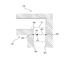
- FIG. 11 is a schematic diagram illustrating an example of measuring the positional deviation of the edge of the terminal pattern as a feature amount.
- the motion control unit 5 determines whether or not the CAD pattern 283 is a terminal pattern by the following determination method. .. That is, the motion control unit 5 determines the edge 284 of the CAD pattern 283 located closest to the measurement point 281.
- the motion control unit 5 determines that the CAD pattern 283 is the terminal pattern.
- the motion control unit 5 detects the edge of the actual pattern on the image corresponding to the edge 284 of the CAD pattern 283 which is the terminal pattern, and the misalignment of the edge of the actual pattern, that is, the edge of the actual pattern and the edge 284 of the CAD pattern 283. Measure the distance to.
- FIG. 12 is a flowchart illustrating the determination of the CAD pattern type and measurement recipe described above.
- the measurement point for specifying the measurement position of the feature amount (for example, dimension) of the pattern on the image is input to the motion control unit 5.
- the measurement point is located in or near the CAD pattern corresponding to the actual pattern to be measured.
- the measurement points are stored in the storage device 5a.
- the motion control unit 5 issues a command to the scanning electron microscope 1 to generate an image of the actual pattern corresponding to the CAD pattern.
- the motion control unit 5 acquires an image of the actual pattern from the scanning electron microscope 1.
- the motion control unit 5 aligns the actual pattern on the image corresponding to the CAD pattern with the CAD pattern.
- a known pattern matching technique can be used to align the actual pattern on the image with the CAD pattern.
- step S4 the motion control unit 5 determines that the CAD pattern is an isolated pattern when the area of the CAD pattern is smaller than the predetermined area. Further, the motion control unit 5 determines whether or not the measurement point is within the CAD pattern. When the measurement point is located within the CAD pattern, in step S5, the motion control unit 5 measures the width of the actual pattern on the image corresponding to the CAD pattern which is the isolated pattern. In one embodiment, the motion control unit 5 may further calculate the area and / or flatness of the actual pattern as the feature amount of the pattern. Further, in one embodiment, the motion control unit 5 may measure the position deviation of the entire actual pattern, that is, the deviation amount between the actual pattern and the corresponding CAD pattern as the feature amount of the pattern.
- step S6 it is determined whether or not the measurement points are located between the isolated patterns.
- step S7 the motion control unit 5 measures the distance between the actual patterns on the image corresponding to the CAD pattern which is the isolated pattern.
- the motion control unit 5 determines whether or not the CAD pattern is a linear pattern. That is, in step S8, in step S8, the first edge of the CAD pattern closest to the measurement point and the second edge beyond the measurement point on the opposite side of the first edge are vertices in a predetermined search region. When the CAD pattern is not provided, the motion control unit 5 determines that the CAD pattern is a linear pattern. Further, the motion control unit 5 determines whether or not the measurement point is within the CAD pattern. When the measurement point is located within the CAD pattern, in step S9, the motion control unit 5 measures the width of the actual pattern on the image corresponding to the CAD pattern which is a linear pattern.
- the motion control unit 5 may further calculate the line edge roughness of the actual pattern as the feature amount of the pattern. Further, in one embodiment, the motion control unit 5 may measure the position deviation of the entire actual pattern, that is, the deviation amount between the actual pattern and the corresponding CAD pattern as the feature amount of the pattern.
- step S10 it is determined whether or not the measurement points are located between the linear patterns.
- step S11 the motion control unit 5 measures the distance between the actual patterns on the image corresponding to the CAD pattern which is the linear pattern.
- step S12 when at least one of the first edge and the second edge has vertices in a predetermined search region, the motion control unit 5 determines that the CAD pattern is a curved pattern. do. Further, the motion control unit 5 determines whether or not the measurement point is within the CAD pattern. When the measurement point is located within the CAD pattern, in step S13, the motion control unit 5 measures the width of the actual pattern on the image corresponding to the CAD pattern which is a curved pattern. In one embodiment, the motion control unit 5 may further calculate the curvature and / or the line edge roughness of the actual pattern as the feature amount of the pattern.
- step S14 it is determined whether or not the measurement points are located between the curve patterns.
- the motion control unit 5 measures the distance between the actual patterns on the image corresponding to the CAD pattern which is the curved pattern.
- step S16 when the length of the edge of the CAD pattern closest to the measurement point is shorter than the predetermined length and the area of the CAD pattern is larger than the predetermined area, the motion control unit 5 determines the CAD pattern. Determined to be the termination pattern.
- step S17 the motion control unit 5 detects the edge of the actual pattern on the image corresponding to the edge of the CAD pattern which is the terminal pattern, and the misalignment of the edge of the actual pattern, that is, the edge of the actual pattern and the edge of the CAD pattern. Measure the distance to.
- the motion control unit 5 ends the feature quantity measuring operation.
- the optimum measurement recipe can be determined based on the relative position between the measurement point and the CAD pattern on the design data and the area of the CAD pattern.
- the present invention relates to a method for measuring a feature quantity such as a pattern dimension (Critical Dimension) on an image generated by an image generator such as a scanning electron microscope, and particularly for workpieces such as wafers, masks, panels, and substrates. It can be used as a method for automatically determining a measurement recipe for features such as the dimensions of a formed pattern.
- a feature quantity such as a pattern dimension (Critical Dimension) on an image generated by an image generator such as a scanning electron microscope, and particularly for workpieces such as wafers, masks, panels, and substrates.
Landscapes
- Engineering & Computer Science (AREA)
- Physics & Mathematics (AREA)
- Computer Vision & Pattern Recognition (AREA)
- General Physics & Mathematics (AREA)
- Theoretical Computer Science (AREA)
- Manufacturing & Machinery (AREA)
- Microelectronics & Electronic Packaging (AREA)
- Computer Hardware Design (AREA)
- Power Engineering (AREA)
- Geometry (AREA)
- Quality & Reliability (AREA)
- Length-Measuring Devices Using Wave Or Particle Radiation (AREA)
- Testing Or Measuring Of Semiconductors Or The Like (AREA)
Priority Applications (3)
| Application Number | Priority Date | Filing Date | Title |
|---|---|---|---|
| US17/925,810 US20230186459A1 (en) | 2020-05-20 | 2021-05-06 | Pattern measuring method |
| KR1020227043907A KR20230012016A (ko) | 2020-05-20 | 2021-05-06 | 패턴 측정 방법 |
| CN202180035695.5A CN115699278A (zh) | 2020-05-20 | 2021-05-06 | 图案测量方法 |
Applications Claiming Priority (2)
| Application Number | Priority Date | Filing Date | Title |
|---|---|---|---|
| JP2020-088016 | 2020-05-20 | ||
| JP2020088016A JP7303155B2 (ja) | 2020-05-20 | 2020-05-20 | パターン測定方法 |
Publications (1)
| Publication Number | Publication Date |
|---|---|
| WO2021235227A1 true WO2021235227A1 (ja) | 2021-11-25 |
Family
ID=78606786
Family Applications (1)
| Application Number | Title | Priority Date | Filing Date |
|---|---|---|---|
| PCT/JP2021/017356 Ceased WO2021235227A1 (ja) | 2020-05-20 | 2021-05-06 | パターン測定方法 |
Country Status (6)
| Country | Link |
|---|---|
| US (1) | US20230186459A1 (enExample) |
| JP (1) | JP7303155B2 (enExample) |
| KR (1) | KR20230012016A (enExample) |
| CN (1) | CN115699278A (enExample) |
| TW (1) | TW202201590A (enExample) |
| WO (1) | WO2021235227A1 (enExample) |
Families Citing this family (2)
| Publication number | Priority date | Publication date | Assignee | Title |
|---|---|---|---|---|
| JP7574157B2 (ja) * | 2021-08-27 | 2024-10-28 | 株式会社ニューフレアテクノロジー | 検査装置及び参照画像生成方法 |
| JP2025144774A (ja) * | 2024-03-21 | 2025-10-03 | 東レエンジニアリング先端半導体Miテクノロジー株式会社 | パターン測定方法およびパターン測定装置 |
Citations (4)
| Publication number | Priority date | Publication date | Assignee | Title |
|---|---|---|---|---|
| JP2007149055A (ja) * | 2005-05-19 | 2007-06-14 | Nano Geometry Kenkyusho:Kk | パターン検査装置および方法 |
| JP2008235575A (ja) * | 2007-03-20 | 2008-10-02 | Toshiba Corp | パターン測定方法、パターン測定装置およびプログラム |
| JP2009243993A (ja) * | 2008-03-31 | 2009-10-22 | Hitachi High-Technologies Corp | 走査型電子顕微鏡を用いた回路パターンの寸法計測装置およびその方法 |
| JP2014025700A (ja) * | 2012-07-24 | 2014-02-06 | Hitachi High-Technologies Corp | パターン計測装置及び方法 |
Family Cites Families (3)
| Publication number | Priority date | Publication date | Assignee | Title |
|---|---|---|---|---|
| JP2011137901A (ja) * | 2009-12-28 | 2011-07-14 | Hitachi High-Technologies Corp | パターン計測条件設定装置 |
| JP2011191296A (ja) * | 2010-03-16 | 2011-09-29 | Ngr Inc | パターン検査装置および方法 |
| JP5438741B2 (ja) | 2011-10-26 | 2014-03-12 | 株式会社アドバンテスト | パターン測定装置及びパターン測定方法 |
-
2020
- 2020-05-20 JP JP2020088016A patent/JP7303155B2/ja active Active
-
2021
- 2021-05-06 KR KR1020227043907A patent/KR20230012016A/ko active Pending
- 2021-05-06 CN CN202180035695.5A patent/CN115699278A/zh active Pending
- 2021-05-06 US US17/925,810 patent/US20230186459A1/en active Pending
- 2021-05-06 WO PCT/JP2021/017356 patent/WO2021235227A1/ja not_active Ceased
- 2021-05-14 TW TW110117504A patent/TW202201590A/zh unknown
Patent Citations (4)
| Publication number | Priority date | Publication date | Assignee | Title |
|---|---|---|---|---|
| JP2007149055A (ja) * | 2005-05-19 | 2007-06-14 | Nano Geometry Kenkyusho:Kk | パターン検査装置および方法 |
| JP2008235575A (ja) * | 2007-03-20 | 2008-10-02 | Toshiba Corp | パターン測定方法、パターン測定装置およびプログラム |
| JP2009243993A (ja) * | 2008-03-31 | 2009-10-22 | Hitachi High-Technologies Corp | 走査型電子顕微鏡を用いた回路パターンの寸法計測装置およびその方法 |
| JP2014025700A (ja) * | 2012-07-24 | 2014-02-06 | Hitachi High-Technologies Corp | パターン計測装置及び方法 |
Also Published As
| Publication number | Publication date |
|---|---|
| TW202201590A (zh) | 2022-01-01 |
| JP2021182601A (ja) | 2021-11-25 |
| KR20230012016A (ko) | 2023-01-25 |
| US20230186459A1 (en) | 2023-06-15 |
| CN115699278A (zh) | 2023-02-03 |
| JP7303155B2 (ja) | 2023-07-04 |
Similar Documents
| Publication | Publication Date | Title |
|---|---|---|
| US8507856B2 (en) | Pattern measuring method and pattern measuring device | |
| US9696150B2 (en) | Overlay error measuring device and computer program | |
| US8295584B2 (en) | Pattern measurement methods and pattern measurement equipment | |
| US8835881B2 (en) | Drift correction method and pattern writing data generation method | |
| WO2013118613A1 (ja) | パターン評価方法およびパターン評価装置 | |
| JP2009252959A (ja) | パターン検査装置、パターン検査方法および半導体装置の製造方法 | |
| WO2021235227A1 (ja) | パターン測定方法 | |
| JP2013172106A (ja) | 描画装置及び物品の製造方法 | |
| JPH0732111B2 (ja) | 荷電ビ−ム投影露光装置 | |
| TWI833505B (zh) | 用於多層結構之基於層的影像偵測及處理 | |
| US5608226A (en) | Electron-beam exposure method and system | |
| JPH05190435A (ja) | 半導体装置の電子線描画方法 | |
| US7476881B2 (en) | Charged beam drawing apparatus and charged beam drawing method | |
| JPS6258621A (ja) | 微細パタ−ン形成方法 | |
| JP2950283B2 (ja) | 電子線アライメント方法及び装置 | |
| JP2023009348A (ja) | パターンエッジの評価方法 | |
| WO2019188296A1 (ja) | 画像生成方法 | |
| TW202105552A (zh) | 畫像產生方法 | |
| JPH11297794A (ja) | ウエハアライメント方法 | |
| WO2025197587A1 (ja) | パターン測定方法およびパターン測定装置 | |
| WO2021210505A1 (ja) | パターンマッチング方法 | |
| CN118401901A (zh) | 基于具有自适应加权的模板匹配的重叠量测 | |
| JPH04112525A (ja) | 直接描画方法 | |
| JPH0464219A (ja) | 荷電粒子線描画装置 |
Legal Events
| Date | Code | Title | Description |
|---|---|---|---|
| 121 | Ep: the epo has been informed by wipo that ep was designated in this application |
Ref document number: 21809377 Country of ref document: EP Kind code of ref document: A1 |
|
| ENP | Entry into the national phase |
Ref document number: 20227043907 Country of ref document: KR Kind code of ref document: A |
|
| NENP | Non-entry into the national phase |
Ref country code: DE |
|
| 122 | Ep: pct application non-entry in european phase |
Ref document number: 21809377 Country of ref document: EP Kind code of ref document: A1 |