WO2021220820A1 - 撮像装置 - Google Patents
撮像装置 Download PDFInfo
- Publication number
- WO2021220820A1 WO2021220820A1 PCT/JP2021/015520 JP2021015520W WO2021220820A1 WO 2021220820 A1 WO2021220820 A1 WO 2021220820A1 JP 2021015520 W JP2021015520 W JP 2021015520W WO 2021220820 A1 WO2021220820 A1 WO 2021220820A1
- Authority
- WO
- WIPO (PCT)
- Prior art keywords
- photoelectric conversion
- electrode
- semiconductor material
- blocking layer
- voltage
- Prior art date
- Legal status (The legal status is an assumption and is not a legal conclusion. Google has not performed a legal analysis and makes no representation as to the accuracy of the status listed.)
- Ceased
Links
Images


Classifications
-
- H—ELECTRICITY
- H10—SEMICONDUCTOR DEVICES; ELECTRIC SOLID-STATE DEVICES NOT OTHERWISE PROVIDED FOR
- H10K—ORGANIC ELECTRIC SOLID-STATE DEVICES
- H10K39/00—Integrated devices, or assemblies of multiple devices, comprising at least one organic radiation-sensitive element covered by group H10K30/00
- H10K39/30—Devices controlled by radiation
- H10K39/32—Organic image sensors
-
- H—ELECTRICITY
- H10—SEMICONDUCTOR DEVICES; ELECTRIC SOLID-STATE DEVICES NOT OTHERWISE PROVIDED FOR
- H10F—INORGANIC SEMICONDUCTOR DEVICES SENSITIVE TO INFRARED RADIATION, LIGHT, ELECTROMAGNETIC RADIATION OF SHORTER WAVELENGTH OR CORPUSCULAR RADIATION
- H10F39/00—Integrated devices, or assemblies of multiple devices, comprising at least one element covered by group H10F30/00, e.g. radiation detectors comprising photodiode arrays
- H10F39/10—Integrated devices
- H10F39/12—Image sensors
- H10F39/191—Photoconductor image sensors
-
- H—ELECTRICITY
- H04—ELECTRIC COMMUNICATION TECHNIQUE
- H04N—PICTORIAL COMMUNICATION, e.g. TELEVISION
- H04N23/00—Cameras or camera modules comprising electronic image sensors; Control thereof
- H04N23/70—Circuitry for compensating brightness variation in the scene
- H04N23/73—Circuitry for compensating brightness variation in the scene by influencing the exposure time
-
- H—ELECTRICITY
- H04—ELECTRIC COMMUNICATION TECHNIQUE
- H04N—PICTORIAL COMMUNICATION, e.g. TELEVISION
- H04N25/00—Circuitry of solid-state image sensors [SSIS]; Control thereof
- H04N25/60—Noise processing, e.g. detecting, correcting, reducing or removing noise
- H04N25/62—Detection or reduction of noise due to excess charges produced by the exposure, e.g. smear, blooming, ghost image, crosstalk or leakage between pixels
-
- H—ELECTRICITY
- H10—SEMICONDUCTOR DEVICES; ELECTRIC SOLID-STATE DEVICES NOT OTHERWISE PROVIDED FOR
- H10F—INORGANIC SEMICONDUCTOR DEVICES SENSITIVE TO INFRARED RADIATION, LIGHT, ELECTROMAGNETIC RADIATION OF SHORTER WAVELENGTH OR CORPUSCULAR RADIATION
- H10F39/00—Integrated devices, or assemblies of multiple devices, comprising at least one element covered by group H10F30/00, e.g. radiation detectors comprising photodiode arrays
- H10F39/80—Constructional details of image sensors
- H10F39/803—Pixels having integrated switching, control, storage or amplification elements
- H10F39/8033—Photosensitive area
-
- H—ELECTRICITY
- H10—SEMICONDUCTOR DEVICES; ELECTRIC SOLID-STATE DEVICES NOT OTHERWISE PROVIDED FOR
- H10K—ORGANIC ELECTRIC SOLID-STATE DEVICES
- H10K30/00—Organic devices sensitive to infrared radiation, light, electromagnetic radiation of shorter wavelength or corpuscular radiation
- H10K30/30—Organic devices sensitive to infrared radiation, light, electromagnetic radiation of shorter wavelength or corpuscular radiation comprising bulk heterojunctions, e.g. interpenetrating networks of donor and acceptor material domains
- H10K30/353—Organic devices sensitive to infrared radiation, light, electromagnetic radiation of shorter wavelength or corpuscular radiation comprising bulk heterojunctions, e.g. interpenetrating networks of donor and acceptor material domains comprising blocking layers, e.g. exciton blocking layers
-
- H—ELECTRICITY
- H10—SEMICONDUCTOR DEVICES; ELECTRIC SOLID-STATE DEVICES NOT OTHERWISE PROVIDED FOR
- H10K—ORGANIC ELECTRIC SOLID-STATE DEVICES
- H10K2101/00—Properties of the organic materials covered by group H10K85/00
- H10K2101/40—Interrelation of parameters between multiple constituent active layers or sublayers, e.g. HOMO values in adjacent layers
-
- Y—GENERAL TAGGING OF NEW TECHNOLOGICAL DEVELOPMENTS; GENERAL TAGGING OF CROSS-SECTIONAL TECHNOLOGIES SPANNING OVER SEVERAL SECTIONS OF THE IPC; TECHNICAL SUBJECTS COVERED BY FORMER USPC CROSS-REFERENCE ART COLLECTIONS [XRACs] AND DIGESTS
- Y02—TECHNOLOGIES OR APPLICATIONS FOR MITIGATION OR ADAPTATION AGAINST CLIMATE CHANGE
- Y02E—REDUCTION OF GREENHOUSE GAS [GHG] EMISSIONS, RELATED TO ENERGY GENERATION, TRANSMISSION OR DISTRIBUTION
- Y02E10/00—Energy generation through renewable energy sources
- Y02E10/50—Photovoltaic [PV] energy
- Y02E10/549—Organic PV cells
Definitions
- the present disclosure relates to an image pickup apparatus using a photoelectric conversion element.
- Patent Document 1 discloses a method in which an electron blocking layer or a hole blocking layer is provided between the photoelectric conversion material and the electrode in order to prevent backflow of electric charge from the electrode.
- Patent Document 2 discloses a method of changing the bias voltage applied to the electrodes connected to both ends of the photoelectric conversion element.
- an object of the present disclosure is to provide an imaging device capable of reducing parasitic sensitivity.
- the imaging device includes a plurality of pixels. Each of the plurality of pixels is located between the first electrode, the second electrode, the first electrode and the second electrode, contains a donor semiconductor material and an acceptor semiconductor material, and is positive for electrons.
- a photoelectric conversion layer that forms a pair with holes, a first charge blocking layer located between the first electrode and the photoelectric conversion layer, and a second electrode located between the second electrode and the photoelectric conversion layer. It includes a two-charge blocking layer and a charge storage region that is electrically connected to the second electrode and stores the holes as signal charges.
- the ionization potential of the second charge blocking layer is equal to or higher than the ionization potential of the donor semiconductor material.
- the electron affinity of the first charge blocking layer is smaller than the electron affinity of the acceptable semiconductor material.
- the difference between the electron affinity of the acceptor semiconductor material and the electron affinity of the first charge blocking layer is larger than the difference between the ionization potential of the donor semiconductor material and the ionization potential of the second charge blocking layer. ..
- the imaging device includes a plurality of pixels.
- Each of the plurality of pixels is located between the first electrode, the second electrode, the first electrode and the second electrode, contains a donor semiconductor material and an acceptor semiconductor material, and is positive with electrons.
- a photoelectric conversion layer that forms a pair with a hole, a first charge blocking layer located between the first electrode and the photoelectric conversion layer, and a second electrode located between the second electrode and the photoelectric conversion layer. It includes a two-charge blocking layer and a charge storage region that is electrically connected to the second electrode and stores the electrons as signal charges.
- the electron affinity of the second charge blocking layer is less than or equal to the electron affinity of the acceptable semiconductor material.
- the ionization potential of the first charge blocking layer is larger than the ionization potential of the donor semiconductor material.
- the difference between the ionization potential of the donor semiconductor material and the ionization potential of the first charge blocking layer is larger than the difference between the electron affinity of the acceptor semiconductor material and the electron affinity of the second charge blocking layer. ..
- an imaging device capable of reducing parasitic sensitivity.
- FIG. 1 is a schematic cross-sectional view showing the configuration of the photoelectric conversion element according to the embodiment.
- FIG. 2 is an exemplary energy band diagram of the photoelectric conversion element according to the embodiment.
- FIG. 3A is an exemplary energy band diagram when a reverse bias voltage is applied in the photoelectric conversion element according to the embodiment.
- FIG. 3B is an exemplary energy band diagram when a forward bias voltage is applied in the photoelectric conversion element according to the embodiment.
- FIG. 4 is a diagram showing an example of the circuit configuration of the image pickup apparatus according to the embodiment.
- FIG. 5 is a schematic cross-sectional view showing a device structure of pixels in the image pickup apparatus according to the embodiment.
- FIG. 6 is a diagram showing an example of typical current-voltage characteristics of the photoelectric conversion layer according to the embodiment.
- FIG. 1 is a schematic cross-sectional view showing the configuration of the photoelectric conversion element according to the embodiment.
- FIG. 2 is an exemplary energy band diagram of the photoelectric conversion element according to the embodiment.
- FIG. 7 is an exemplary energy band diagram of another photoelectric conversion element according to the present embodiment.
- FIG. 8 is a diagram showing a part of a schematic circuit configuration of pixels according to the embodiment.
- FIG. 9 is a timing chart showing an example of the voltage supplied to the upper electrode of the photoelectric conversion unit according to the embodiment and the operation timing in each row of the pixel array of the image pickup apparatus.
- FIG. 10 is a timing chart showing an example of an operation of adjusting the sensitivity of photoelectric conversion by a pulse duty control method in the image pickup apparatus according to the embodiment.
- FIG. 11 is a diagram showing a schematic configuration of a photoelectric conversion element in an embodiment.
- FIG. 12 is a diagram showing a schematic configuration of a photoelectric conversion element in a comparative example.
- FIG. 13 is a diagram showing current densities in light and dark when a bias voltage is applied to the photoelectric conversion element in the embodiment.
- FIG. 14 is a diagram showing current densities in light and dark when a bias voltage is applied to the photoelectric conversion element in the comparative example.
- the imaging device includes a plurality of pixels. Each of the plurality of pixels is located between the first electrode, the second electrode, the first electrode and the second electrode, contains a donor semiconductor material and an acceptor semiconductor material, and is positive for electrons.
- a photoelectric conversion layer that forms a pair with holes, a first charge blocking layer located between the first electrode and the photoelectric conversion layer, and a second electrode located between the second electrode and the photoelectric conversion layer. It includes a two-charge blocking layer and a charge storage region that is electrically connected to the second electrode and stores the holes as signal charges.
- the ionization potential of the second charge blocking layer is equal to or higher than the ionization potential of the donor semiconductor material.
- the electron affinity of the first charge blocking layer is smaller than the electron affinity of the acceptable semiconductor material.
- the difference between the electron affinity of the acceptor semiconductor material and the electron affinity of the first charge blocking layer is larger than the difference between the ionization potential of the donor semiconductor material and the ionization potential of the second charge blocking layer. ..
- the holes accumulated in the charge storage region are read out as signal charges, the electrons that tend to remain in the photoelectric conversion layer remain in the photoelectric conversion layer at the timing when the movement of the holes to the charge storage region is desired to be stopped.
- the recombination of holes is promoted without any shortage.
- the movement of holes to the charge storage region is suppressed regardless of the amount of light applied to the photoelectric conversion layer. Therefore, the parasitic sensitivity in the imaging device can be reduced.
- the difference between the electron affinity of the acceptor semiconductor material and the electron affinity of the first charge blocking layer is the ionization potential of the donor semiconductor material and the ionization potential of the second charge blocking layer. It may be 0.1 eV or more larger than the difference between the two.
- the energy barrier when the electrons generated in the photoelectric conversion layer move to the first electrode becomes sufficiently larger than the energy barrier when the holes generated in the photoelectric conversion layer move to the second electrode. Therefore, the parasitic sensitivity in the imaging device can be further reduced.
- the first charge blocking layer may contain the donor semiconductor material.
- the imaging device includes a plurality of pixels.
- Each of the plurality of pixels is located between the first electrode, the second electrode, the first electrode and the second electrode, contains a donor semiconductor material and an acceptor semiconductor material, and is positive with electrons.
- a photoelectric conversion layer that forms a pair with a hole, a first charge blocking layer located between the first electrode and the photoelectric conversion layer, and a second electrode located between the second electrode and the photoelectric conversion layer. It includes a two-charge blocking layer and a charge storage region that is electrically connected to the second electrode and stores the electrons as signal charges.
- the electron affinity of the second charge blocking layer is less than or equal to the electron affinity of the acceptable semiconductor material.
- the ionization potential of the first charge blocking layer is larger than the ionization potential of the donor semiconductor material.
- the difference between the ionization potential of the donor semiconductor material and the ionization potential of the first charge blocking layer is larger than the difference between the electron affinity of the acceptor semiconductor material and the electron affinity of the second charge blocking layer. ..
- the electrons accumulated in the charge storage region are read out as signal charges, the holes that tend to remain in the photoelectric conversion layer remain in the photoelectric conversion layer at the timing when the movement of the electrons to the charge storage region is desired to be stopped. By recombination with the existing electrons, the electrons are likely to disappear. As a result, the movement of electrons to the charge storage region is suppressed regardless of the amount of light emitted to the photoelectric conversion layer. Therefore, the parasitic sensitivity in the imaging device can be reduced.
- the imaging device further includes a voltage supply circuit that is electrically connected to the first electrode and provides a potential difference between the first electrode and the second electrode, and the voltage supply circuit is the first.
- a first voltage may be supplied to one electrode in the first period, and a second voltage different from the first voltage may be supplied in the second period.
- the timing of photoelectric conversion and the timing of reading can be separated, and the parasitic sensitivity can be further reduced.
- the photoelectric conversion efficiency of the plurality of pixels in the first period may be different from the photoelectric conversion efficiency of the plurality of pixels in the second period.
- the first voltage and the second voltage are selected so that the change in the current density differs depending on the amount of light incident on the photoelectric conversion layer.
- the parasitic sensitivity can be reduced by recombining the holes and electrons in the photoelectric conversion layer during the period when the change becomes small.
- the imaging device may operate in a global shutter system in which the timing of the exposure period is unified among the plurality of pixels, and the signal charge is accumulated in the charge storage region during the exposure period. You may.
- the first period may be the exposure period
- the second period may be a non-exposure period different from the exposure period
- the global shutter method can be realized while reducing the parasitic sensitivity in the second period.
- the electrons and the holes may be recombinated in the photoelectric conversion layer by supplying the second voltage to the first electrode by the voltage supply circuit.
- the second period which is the non-exposure period
- the second period is set as the signal readout period, so that the photoelectric is photoelectric in the non-exposure period.
- the current density generated from the conversion layer is less likely to be affected by the amount of light incident on the photoelectric conversion layer. Therefore, the parasitic sensitivity can be reduced in the second period.
- the sensitivity of photoelectric conversion may be generated in the photoelectric conversion layer.
- the voltage that causes the sensitivity of the photoelectric conversion layer is supplied to the first electrode, so that an imaging device capable of reducing the parasitic sensitivity while improving the S / N ratio is realized. can.
- the first period and the second period are included in any one or more exposure periods in the same frame, and in the one or more exposure periods, the signal charge is generated in the charge storage region. It may be accumulated.
- any one or more exposure periods in the same frame include a first period and a second period in which different voltages are supplied to the first electrode. Therefore, the image pickup apparatus can adjust the magnitude of the first voltage and the second voltage, or the length of the first period and the second period to adjust the sensitivity of the photoelectric conversion. Therefore, in such an imaging device having an electronic ND (Neutral Density) function, the parasitic sensitivity can be reduced.
- ND Neutral Density
- the donor semiconductor material may be a donor organic semiconductor material
- the acceptor semiconductor material may be an acceptor organic semiconductor material
- the thickness of the first charge blocking layer may be 5 nm or more.
- the thickness of the second charge blocking layer may be 5 nm or more.
- FIG. 1 is a schematic cross-sectional view showing the configuration of the photoelectric conversion element 10 according to the present embodiment.
- the photoelectric conversion element 10 is supported by the support substrate 1 and is located between the upper electrode 6 and the lower electrode 2 which are a pair of electrodes and the upper electrode 6 and the lower electrode 2. It includes a photoelectric conversion layer 4, a hole blocking layer 5 located between the upper electrode 6 and the photoelectric conversion layer 4, and an electron blocking layer 3 located between the lower electrode 2 and the photoelectric conversion layer 4.
- the upper electrode 6 is an example of the first electrode
- the lower electrode 2 is an example of the second electrode
- the hole blocking layer 5 is an example of the first charge blocking layer
- the electron blocking layer 3 is an example of the second charge blocking layer.
- the support substrate 1 may be any substrate used to support a general photoelectric conversion element, and may be, for example, a glass substrate, a quartz substrate, a semiconductor substrate, a plastic substrate, or the like.
- the lower electrode 2 is formed of metal, metal nitride, metal oxide, polysilicon to which conductivity is imparted, or the like.
- metals include aluminum, copper, titanium and tungsten.
- methods for imparting conductivity to polysilicon include doping with impurities.
- the upper electrode 6 is, for example, a transparent electrode formed of a transparent conductive material.
- the material of the upper electrode 6 include transparent conductive oxide (TCO: Transpartic Conducting Oxide), ITO (Indium Tin Oxide), IZO (Indium Zinc Oxide), AZO (Aluminum-topped Zinc Oxide), and FTO (FTO). Doped Tin Oxide), SnO 2 and TiO 2 and the like.
- the upper electrode 6 may be made of TCO and metal materials such as aluminum (Al) and gold (Au) individually or in combination, depending on the desired transmittance.
- the material of the lower electrode 2 and the upper electrode 6 is not limited to the above-mentioned conductive material, and other materials may be used.
- the lower electrode 2 may be a transparent electrode.
- the lower electrode 2 and the upper electrode 6 are used for manufacturing the lower electrode 2 and the upper electrode 6 depending on the material used.
- a method such as an electron beam method, a sputtering method, a resistance heating vapor deposition method, a chemical reaction method such as a sol-gel method, or a coating of a dispersion of indium tin oxide may be used.
- the lower electrode 2 and the upper electrode 6 may be further subjected to UV-ozone treatment, plasma treatment, or the like after the ITO film is formed.
- the photoelectric conversion layer 4 contains a donor semiconductor material and an acceptor semiconductor material.
- the photoelectric conversion layer 4 is made of, for example, an organic semiconductor material.
- a wet method such as a coating method by spin coating or a dry method such as a vacuum vapor deposition method can be used.
- the vacuum vapor deposition method is a method in which the material of the layer is vaporized by heating under vacuum and deposited on the substrate.
- the photoelectric conversion layer 4 is, for example, a mixed film having a bulk heterostructure containing a donor organic semiconductor material and an acceptor organic semiconductor material.
- the photoelectric conversion layer 4 is easily formed as a thin film by containing the donor organic semiconductor material and the acceptor organic semiconductor material.
- donor organic semiconductor materials and acceptor organic semiconductor materials will be specifically exemplified.
- donor organic semiconductor materials include triarylamine compounds, benzidine compounds, pyrazoline compounds, styrylamine compounds, hydrazone compounds, triphenylmethane compounds, carbazole compounds, polysilane compounds, thiophene compounds, phthalocyanine compounds, naphthalocyanine compounds, and subs.
- Acceptable organic semiconductor materials include, for example, fullerene (eg, C60 fullerene and C70 fullerene, etc.), fullerene derivatives (eg, PCBM (phenyl C 61 butyrate methyl ester) and ICBA (inden C 60 bis adduct), etc.), condensation.
- a 5- to 7-membered heterocyclic compounds containing aromatic carbocyclic compounds eg, naphthalene derivatives, anthracene derivatives, phenanthrene derivatives, tetracene derivatives, pyrene derivatives, perylene derivatives, fluorantene derivatives, etc.
- nitrogen atoms oxygen atoms, and sulfur atoms.
- Benzoxazole benzothiazole, carbazole, purine, triazolopyridazine, triazolopyrimidine, tetrazyneden, oxadiazol, imidazolepyridine, pyrrolidine, pyroloppyridine, thiadiazolopyridine, dibenzazepine and tribenzazepine, etc.
- polyarylene examples thereof include a metal complex having a compound, a fluorene compound, a cyclopentadiene compound, a silyl compound and a nitrogen-containing heterocyclic compound as ligands.
- the donor organic semiconductor material and the acceptor organic semiconductor material are not limited to the above examples. If it is an organic compound that can be formed as a photoelectric conversion layer by either a dry method or a wet method, a low molecular weight organic compound and a high molecular weight organic compound can be used as a donor organic semiconductor material and an acceptor property constituting the photoelectric conversion layer 4. It may be used as an organic semiconductor material.
- the photoelectric conversion layer 4 may include a semiconductor material other than the above as a donor semiconductor material and an acceptor semiconductor material.
- the photoelectric conversion layer 4 may contain, for example, a silicon semiconductor, a compound semiconductor, a quantum dot, a perovskite material, a carbon nanotube, or a mixture of any two or more of them as a semiconductor material.
- the photoelectric conversion element 10 has holes provided between the electron blocking layer 3 provided between the lower electrode 2 and the photoelectric conversion layer 4 and between the upper electrode 6 and the photoelectric conversion layer 4.
- the blocking layer 5 is provided.
- the thickness of the electron blocking layer 3 is, for example, 5 nm or more. This makes it easier to secure the function of the electron blocking layer 3. Further, the thickness of the electron blocking layer 3 may be 100 nm or less from the viewpoint of suppressing a decrease in the photoelectric conversion efficiency of the photoelectric conversion element 10.
- the thickness of the hole blocking layer 5 is, for example, 5 nm or more. This makes it easier to secure the function of the hole blocking layer 5. Further, the thickness of the hole blocking layer 5 may be 100 nm or less from the viewpoint of suppressing a decrease in the photoelectric conversion efficiency of the photoelectric conversion element 10.
- the electron blocking layer 3 and the hole blocking layer 5 are formed of, for example, an organic semiconductor material.
- the material forming the electron blocking layer 3 and the hole blocking layer 5 is not limited to the organic semiconductor material, and may be an oxide semiconductor, a nitride semiconductor, or the like, or a composite material thereof.
- the hole blocking layer 5 may contain a donor organic semiconductor material contained in the photoelectric conversion layer 4 as a main material.
- the hole blocking layer 5 is made of, for example, a donor organic semiconductor material contained in the photoelectric conversion layer 4. Since the hole blocking layer 5 contains the donor organic semiconductor material contained in the photoelectric conversion layer 4, the photoelectric conversion element 10 can be realized with a smaller number of materials. Further, when the photoelectric conversion layer 4 and the hole blocking layer 5 are in contact with each other as shown in the drawing, the hole blocking layer 5 contains the same donor organic semiconductor material as the photoelectric conversion layer 4, so that the photoelectric conversion layer is formed. The adhesion of the interface between 4 and the hole blocking layer 5 is improved.
- FIG. 2 is an exemplary energy band diagram of the photoelectric conversion element 10 shown in FIG. In FIG. 2, the energy band of each layer is shown as a rectangle.
- the photoelectric conversion layer 4 is irradiated with light to generate a pair of electrons and holes inside.
- the generated pair of electrons and holes is separated into electrons and holes by the electric field applied to the photoelectric conversion layer 4.
- the electrons and holes move to the lower electrode 2 side or the upper electrode 6 side according to the electric field, respectively.
- the semiconductor material that donates electrons to the other material is the donor semiconductor material
- the semiconductor material that accepts the electrons is the acceptor semiconductor material.
- the donor organic semiconductor material is an example of a donor semiconductor material
- the acceptor organic semiconductor material is an example of an acceptor semiconductor material.
- the donor semiconductor material When the photoelectric conversion layer 4 is irradiated with light, for example, the donor semiconductor material generates a pair of electrons and holes to donate electrons to the acceptor semiconductor material.
- the donor semiconductor material When two different types of organic semiconductor materials are used, which is the donor semiconductor material and which is the acceptor semiconductor material is generally determined by the HOMO (Highest-Occupied-Molecular-Orbital) of each of the two types of organic semiconductor materials at the contact interface.
- LUMO Large-Unoccupied-Molecular-Orbital
- the relative position of the energy level Of the rectangles showing the energy band in FIG. 2, the upper end is the LUMO energy level and the lower end is the HOMO energy level.
- the one having the smaller electron affinity which is the energy difference between the vacuum level and the LUMO energy level
- the donor organic semiconductor material 4A is the donor organic semiconductor material 4A.
- the larger one is the acceptor-type organic semiconductor material 4B, which is the acceptor-type semiconductor material.
- the ionization potential of the electron blocking layer 3 which is the energy difference between the vacuum level and the energy level of HOMO, is the photoelectric conversion layer. It is equal to or higher than the ionization potential of the donor organic semiconductor material 4A of 4. Further, the electron affinity of the electron blocking layer 3 is, for example, equal to or less than the electron affinity of the acceptor-type organic semiconductor material 4B of the photoelectric conversion layer 4.
- the electron affinity of the hole blocking layer 5 is smaller than the electron affinity of the acceptor-type organic semiconductor material 4B of the photoelectric conversion layer 4.
- the ionization potential of the hole blocking layer 5 is, for example, equal to or higher than the ionization potential of the donor organic semiconductor material 4A of the photoelectric conversion layer 4.
- the difference in electron affinity between the hole blocking layer 5 shown by ⁇ E2 in FIG. 2 and the acceptor-type organic semiconductor material 4B of the photoelectric conversion layer 4 is the difference between the electron blocking layer 3 shown by ⁇ E1 in FIG. 2 and the photoelectric conversion. It is larger than the difference in ionization potential of layer 4 from the donor organic semiconductor material 4A.
- the material of the electron blocking layer 3 and the hole blocking layer 5 for example, from the donor organic semiconductor material and the acceptor organic semiconductor material exemplified above, the above-mentioned materials having a magnitude relationship of energy are used.
- the lower electrode 2 is electrically connected to the charge storage node 34, which will be described later.
- the charge storage node 34 which is an example of the charge storage region, stores holes generated in the photoelectric conversion layer 4.
- FIG. 3A is an exemplary energy band diagram of the photoelectric conversion element 10 when a voltage acting as a bias in the opposite direction is applied between the lower electrode 2 and the upper electrode 6.
- FIG. 3B is an exemplary energy band diagram of the photoelectric conversion element 10 when a voltage serving as a forward bias is applied between the lower electrode 2 and the upper electrode 6.
- the voltage when a voltage higher than that of the lower electrode 2 is applied to the upper electrode 6 is a reverse bias, that is, a so-called reverse bias voltage, and a voltage lower than that of the lower electrode 2 is applied to the upper electrode 6. It is assumed that the voltage in the case is a forward bias, that is, a so-called forward bias voltage, and the following description will be given.
- the energy barrier when holes move from the photoelectric conversion layer 4 to the lower electrode 2 becomes ⁇ E1
- the energy barrier when electrons move from the photoelectric conversion layer 4 to the upper electrode 6 becomes ⁇ E1.
- the photoelectric conversion element 10 provided in the image pickup apparatus 100 uses the electron blocking layer 3 and the hole blocking layer 5 having the above-mentioned energy band to form holes from the lower electrode 2. It is possible to effectively reduce the parasitic sensitivity in the method of reading out.
- FIG. 4 is a diagram showing an example of a circuit configuration of an image pickup apparatus 100 on which a photoelectric conversion unit 10A using the photoelectric conversion element 10 shown in FIG. 1 is mounted.
- FIG. 5 is a schematic cross-sectional view showing an example of the device structure of the pixel 24 in the image pickup apparatus 100 according to the present embodiment.
- the image pickup apparatus 100 includes a semiconductor substrate 40 and a plurality of pixels 24.
- Each of the plurality of pixels 24 is electrically connected to the charge detection circuit 35 provided on the semiconductor substrate 40, the photoelectric conversion unit 10A provided on the semiconductor substrate 40, and the charge detection circuit 35 and the photoelectric conversion unit 10A.
- the charge storage node 34 is included.
- the photoelectric conversion unit 10A of the plurality of pixels 24 includes the photoelectric conversion element 10. That is, each of the plurality of pixels 24 includes an upper electrode 6, a lower electrode 2, a photoelectric conversion layer 4, a hole blocking layer 5, an electron blocking layer 3, and a charge storage node 34.
- the charge storage node 34 is an example of a charge storage region.
- the charge storage node 34 stores the charge obtained by the photoelectric conversion unit 10A, and the charge detection circuit 35 detects the charge stored in the charge storage node 34.
- the charge detection circuit 35 provided on the semiconductor substrate 40 may be provided on the semiconductor substrate 40 or may be provided in the semiconductor substrate 40.
- the image pickup apparatus 100 includes a plurality of pixels 24 and peripheral circuits.
- the image pickup apparatus 100 is an organic image sensor realized by a one-chip integrated circuit, and has a pixel array PA including a plurality of pixels 24 arranged two-dimensionally.
- the image pickup apparatus 100 is, for example, an image pickup apparatus that operates in a global shutter system in which an exposure period is unified among a plurality of pixels 24. That is, the image pickup apparatus 100 has a global shutter function. The details of the exposure period will be described later.
- the plurality of pixels 24 are arranged two-dimensionally on the semiconductor substrate 40, that is, in the row direction and the column direction to form a photosensitive region which is a pixel region.
- FIG. 4 shows an example in which the pixels 24 are arranged in a matrix of 2 rows and 2 columns. Note that, for convenience of illustration, FIG. 4 omits the illustration of a circuit (for example, a pixel electrode control circuit) for individually setting the sensitivity of the pixel 24.
- the image pickup apparatus 100 may be a line sensor.
- the plurality of pixels 24 may be arranged one-dimensionally.
- the row direction and the column direction mean the directions in which the rows and columns are extended, respectively. That is, in FIG. 4, the vertical direction on the paper surface is the column direction, and the horizontal direction is the row direction.
- each pixel 24 includes a photoelectric conversion unit 10A and a charge storage node 34 electrically connected to the charge detection circuit 35.
- the charge detection circuit 35 includes an amplification transistor 21, a reset transistor 22, and an address transistor 23.
- the photoelectric conversion unit 10A includes a lower electrode 2 provided as a pixel electrode and an upper electrode 6 provided as a counter electrode.
- the photoelectric conversion unit 10A includes the above-mentioned photoelectric conversion element 10.
- a voltage for applying a predetermined bias voltage is supplied to the upper electrode 6 via the counter electrode signal line 26.
- the lower electrode 2 is connected to the gate electrode 21G of the amplification transistor 21, and the signal charge collected by the lower electrode 2 is stored in the charge storage node 34 located between the lower electrode 2 and the gate electrode 21G of the amplification transistor 21. Will be done.
- the signal charge is a hole. That is, the charge storage node 34 is electrically connected to the lower electrode 2 and stores holes generated in the photoelectric conversion layer 4.
- the signal charge accumulated in the charge storage node 34 is applied to the gate electrode 21G of the amplification transistor 21 as a voltage corresponding to the amount of the signal charge.
- the amplification transistor 21 amplifies this voltage and selectively reads it as a signal voltage by the address transistor 23.
- the source / drain electrode of the reset transistor 22 is connected to the lower electrode 2 and resets the signal charge stored in the charge storage node 34. In other words, the reset transistor 22 resets the potentials of the gate electrode 21G and the lower electrode 2 of the amplification transistor 21.
- the image pickup apparatus 100 includes a power supply wiring 31, a vertical signal line 27, an address signal line 36, and a reset signal line 37, and these lines are included. Is connected to each pixel 24, respectively.
- the power supply wiring 31 is connected to the source / drain electrode of the amplification transistor 21, and the vertical signal line 27 is connected to the source / drain electrode of the address transistor 23.
- the address signal line 36 is connected to the gate electrode 23G of the address transistor 23.
- the reset signal line 37 is connected to the gate electrode 22G of the reset transistor 22.
- the peripheral circuit includes a voltage supply circuit 19, a vertical scanning circuit 25, a horizontal signal readout circuit 20, a plurality of column signal processing circuits 29, a plurality of load circuits 28, and a plurality of differential amplifiers 32.
- the voltage supply circuit 19 is electrically connected to the upper electrode 6 via the counter electrode signal line 26.
- the voltage supply circuit 19 supplies a voltage to the upper electrode 6 to give a potential difference between the upper electrode 6 and the lower electrode 2.
- the voltage supply circuit 19 supplies a first voltage in a first period such as an exposure period, which will be described later, and supplies a second voltage different from the first voltage in a second period such as a non-exposure period.
- the vertical scanning circuit 25 is connected to the address signal line 36 and the reset signal line 37, selects a plurality of pixels 24 arranged in each line in line units, reads out the signal voltage, and resets the potential of the lower electrode 2. conduct.
- the power supply wiring 31 which is a source follower power supply supplies a predetermined power supply voltage to each pixel 24.
- the horizontal signal reading circuit 20 is electrically connected to a plurality of column signal processing circuits 29.
- the column signal processing circuit 29 is electrically connected to the pixels 24 arranged in each row via the vertical signal lines 27 corresponding to each row.
- the load circuit 28 is electrically connected to each vertical signal line 27.
- the load circuit 28 and the amplification transistor 21 form a source follower circuit.
- a plurality of differential amplifiers 32 are provided corresponding to each row.
- the negative input terminal of the differential amplifier 32 is connected to the corresponding vertical signal line 27.
- the output terminal of the differential amplifier 32 is connected to the pixel 24 via a feedback line 33 corresponding to each row.
- the vertical scanning circuit 25 applies a row selection signal for controlling the on / off of the address transistor 23 to the gate electrode 23G of the address transistor 23 by the address signal line 36. As a result, the line to be read is scanned and selected. A signal voltage is read from the pixels 24 in the selected row to the vertical signal line 27. Further, the vertical scanning circuit 25 applies a reset signal for controlling the on / off of the reset transistor 22 to the gate electrode 22G of the reset transistor 22 via the reset signal line 37. As a result, the row of pixels 24 that is the target of the reset operation is selected. The vertical signal line 27 transmits the signal voltage read from the pixel 24 selected by the vertical scanning circuit 25 to the column signal processing circuit 29.
- the column signal processing circuit 29 performs noise suppression signal processing represented by correlated double sampling, analog-to-digital conversion (AD conversion), and the like.
- the horizontal signal reading circuit 20 sequentially reads signals from a plurality of column signal processing circuits 29 to a horizontal common signal line (not shown).
- the differential amplifier 32 is connected to the drain electrode of the reset transistor 22 via the feedback line 33. Therefore, the differential amplifier 32 receives the output value of the address transistor 23 at the negative terminal.
- the differential amplifier 32 performs a feedback operation so that the gate potential of the amplification transistor 21 becomes a predetermined feedback voltage. At this time, the output voltage value of the differential amplifier 32 is 0V or a positive voltage in the vicinity of 0V.
- the feedback voltage means the output voltage of the differential amplifier 32.
- the pixel 24 includes a semiconductor substrate 40, a charge detection circuit 35, a photoelectric conversion unit 10A, and a charge storage node 34 (see FIG. 4).
- the semiconductor substrate 40 may be an insulating substrate or the like in which a semiconductor layer is provided on the surface on the side where the photosensitive region is formed, and is, for example, a p-type silicon substrate.
- the semiconductor substrate 40 has impurity regions 21D, 21S, 22D, 22S and 23S, and an element separation region 41 for electrical separation between the pixels 24.
- the impurity regions 21D, 21S, 22D, 22S and 23S are, for example, n-type regions.
- the element separation region 41 is provided between the impurity region 21D and the impurity region 22D. As a result, leakage of the signal charge accumulated in the charge storage node 34 is suppressed.
- the device separation region 41 is formed, for example, by implanting acceptor ions under predetermined implantation conditions.
- the impurity regions 21D, 21S, 22D, 22S and 23S are, for example, diffusion regions formed in the semiconductor substrate 40.
- the amplification transistor 21 includes an impurity region 21S, an impurity region 21D, and a gate electrode 21G.
- the impurity region 21S and the impurity region 21D function as, for example, a source region and a drain region of the amplification transistor 21, respectively.
- a channel region of the amplification transistor 21 is formed between the impurity region 21S and the impurity region 21D.
- the address transistor 23 includes an impurity region 23S and an impurity region 21S, and a gate electrode 23G connected to the address signal line 36.
- the amplification transistor 21 and the address transistor 23 are electrically connected to each other by sharing the impurity region 21S.
- the impurity region 23S functions as, for example, a source region of the address transistor 23.
- the impurity region 23S has a connection with the vertical signal line 27 shown in FIG.
- the reset transistor 22 includes impurity regions 22D and 22S and a gate electrode 22G connected to the reset signal line 37.
- the impurity region 22S functions as, for example, a source region of the reset transistor 22.
- the impurity region 22S has a connection with the reset signal line 37 shown in FIG.
- An interlayer insulating layer 50 is laminated on the semiconductor substrate 40 so as to cover the amplification transistor 21, the address transistor 23, and the reset transistor 22.
- a wiring layer (not shown) may be arranged in the interlayer insulating layer 50.
- the wiring layer is formed of, for example, a metal such as copper, and may include, for example, wiring such as the above-mentioned vertical signal line 27 as a part thereof.
- the number of layers of the insulating layer in the interlayer insulating layer 50 and the number of layers included in the wiring layer arranged in the interlayer insulating layer 50 can be arbitrarily set.
- a contact plug 53 electrically connected to the gate electrode 21G of the amplification transistor 21, a contact plug 54 connected to the impurity region 22D of the reset transistor 22, and a contact plug connected to the lower electrode 2 51, and a wiring 52 connecting the contact plug 51, the contact plug 54, and the contact plug 53 are arranged.
- the impurity region 22D of the reset transistor 22 is electrically connected to the gate electrode 21G of the amplification transistor 21.
- the contact plugs 51, 53 and 54, the wiring 52, the gate electrode 21G of the amplification transistor 21, and the impurity region 22D of the reset transistor 22 constitute at least one part of the charge storage node 34. ..
- the charge detection circuit 35 detects the signal charge captured by the lower electrode 2 and outputs the signal voltage.
- the charge detection circuit 35 includes an amplification transistor 21, a reset transistor 22, and an address transistor 23, and is formed on the semiconductor substrate 40.
- the amplification transistor 21 is formed in the semiconductor substrate 40 and functions as a drain electrode and a source electrode, respectively, on the impurity region 21D and the impurity region 21S, on the gate insulating layer 21X formed on the semiconductor substrate 40, and on the gate insulating layer 21X. Includes a gate electrode 21G formed in.
- the reset transistor 22 is formed on the semiconductor substrate 40 and functions as a drain electrode and a source electrode, respectively, on the impurity region 22D and the impurity region 22S, the gate insulating layer 22X formed on the semiconductor substrate 40, and the gate insulating layer 22X. Includes a gate electrode 22G formed in.
- the address transistor 23 is formed on the impurity regions 21S and 23S formed in the semiconductor substrate 40 and functioning as drain electrodes and source electrodes, respectively, the gate insulating layer 23X formed on the semiconductor substrate 40, and the gate insulating layer 23X. Includes the gate electrode 23G and the like.
- the impurity region 21S is connected in series with the amplification transistor 21 and the address transistor 23.
- the above-mentioned photoelectric conversion unit 10A is arranged on the interlayer insulating layer 50.
- a plurality of pixels 24 constituting the pixel array PA are formed on the semiconductor substrate 40.
- the plurality of pixels 24 arranged two-dimensionally on the semiconductor substrate 40 form a photosensitive region.
- the distance between two adjacent pixels 24 (that is, the pixel pitch) may be, for example, about 2 ⁇ m.
- the photoelectric conversion unit 10A has the structure of the photoelectric conversion element 10 described above.
- a color filter 60 is formed above the photoelectric conversion unit 10A, and a microlens 61 is formed above the color filter 60.
- the color filter 60 is formed as, for example, an on-chip color filter by patterning, and a photosensitive resin or the like in which a dye or a pigment is dispersed is used.
- the microlens 61 is formed as, for example, an on-chip microlens, and an ultraviolet photosensitive material or the like is used.
- a general semiconductor manufacturing process can be used for manufacturing the image pickup apparatus 100.
- various silicon semiconductor processes can be used.
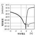
- FIG. 6 is a diagram showing an example of typical current-voltage (IV) characteristics of the photoelectric conversion layer 4.
- the thick solid line graph shows the exemplary IV characteristics of the photoelectric conversion layer 4 when a voltage is applied between the lower electrode 2 and the upper electrode 6 in a state of being irradiated with light.
- an example of the IV characteristic of the photoelectric conversion layer 4 when a voltage is applied between the lower electrode 2 and the upper electrode 6 in a state where no light is irradiated is also shown by a thick broken line. It is also shown.
- the photocurrent characteristics of the photoelectric conversion layer 4 according to the present embodiment are roughly characterized by a first voltage range, a second voltage range, and a third voltage range.
- the first voltage range the dependence of the current change of the photoelectric conversion layer 4 on the bias voltage applied between the lower electrode 2 and the upper electrode 6 and the amount of light incident on the photoelectric conversion layer 4 is small. That is, in the first voltage range, it can be considered that the difference between the current value flowing when there is light incident on the photoelectric conversion layer 4 and the current value flowing when there is no light incident is small.
- the absolute value of the voltage applied between the lower electrode 2 and the upper electrode 6 is not large even if a pair of holes and electrons is generated by the incident of light on the photoelectric conversion layer 4. Therefore, these recombinations occur before the holes and electrons are separated.
- the second voltage range in FIG. 6 is a reverse bias voltage range, which is a region in which the absolute value of the output current density increases as the bias voltage in the reverse direction increases. That is, the second voltage range is a region in which the current value increases as the amount of light incident on the photoelectric conversion layer 4 and the bias voltage applied between the lower electrode 2 and the upper electrode 6 increase.
- the third voltage range is a forward bias voltage range, which is a region in which the output current density increases as the forward bias voltage increases. That is, the third voltage range is a region in which the current increases as the bias voltage applied between the lower electrode 2 and the upper electrode 6 increases even if there is no light incident on the photoelectric conversion layer 4.
- FIG. 3A described above corresponds to an exemplary energy band diagram when a bias voltage in the second voltage range is applied to the photoelectric conversion element 10.
- FIG. 3B corresponds to an exemplary energy band diagram when a bias voltage in the first voltage range is applied to the photoelectric conversion element 10.
- the photoelectric conversion unit 10A composed of the photoelectric conversion element 10 of the image pickup apparatus 100 according to the present embodiment has a current value that flows when there is light incident on the photoelectric conversion layer 4 and a case where there is no light incident.
- the image pickup apparatus 100 can realize the global shutter function while reducing the parasitic sensitivity.
- the difference in electron affinity between the accepting organic semiconductor material 4B and the hole blocking layer 5 ⁇ E2 is the donor organic.
- the difference in electron affinity between the accepting organic semiconductor material 4B and the hole blocking layer 5 ⁇ E2 is the ionization potential of the donor organic semiconductor material 4A and the electron blocking layer 3. It may be 0.1 eV or more larger than the difference ⁇ E1.
- the difference in electron affinity between the accepting organic semiconductor material 4B and the hole blocking layer 5 ⁇ E2 is the difference in ionization potential between the donor organic semiconductor material 4A and the electron blocking layer 3. It may be 0.3 eV or more larger than ⁇ E1.
- the image pickup apparatus includes the upper electrode 6, the lower electrode 2, the photoelectric conversion layer 4 located between the upper electrode 6 and the lower electrode 2, and the lower electrode 2 and the photoelectric conversion layer 4.
- a hole blocking layer located between the two, an electron blocking layer located between the upper electrode 6 and the photoelectric conversion layer 4, and a charge storage node 34 electrically connected to the lower electrode 2 to store electrons.
- FIG. 7 is an exemplary energy band diagram of another photoelectric conversion element according to the present embodiment.
- FIG. 7 shows, as another example of the photoelectric conversion element in the imaging device according to the present embodiment, the photoelectric conversion layer 4 located between the upper electrode 6, the lower electrode 2, and the upper electrode 6 and the lower electrode 2.
- the energy band of the photoelectric conversion element including the hole blocking layer 5A located between the lower electrode 2 and the photoelectric conversion layer 4 and the electron blocking layer 3A located between the upper electrode 6 and the photoelectric conversion layer 4. It is shown.
- the electron affinity of the hole blocking layer 5A is equal to or less than the electron affinity of the acceptor semiconductor material 4B, and the ionization potential of the electron blocking layer 3A is larger than the ionization potential of the donor semiconductor material 4A.
- the difference ⁇ E4 in the ionization potential between the donor organic semiconductor material 4A and the electron blocking layer 3A of the photoelectric conversion layer 4 is the difference in the electron affinity between the acceptor organic semiconductor material 4B and the hole blocking layer 5A of the photoelectric conversion layer 4.
- the configuration is larger than ⁇ E3.
- the photoelectric conversion layer 4 is positive by the same mechanism as the image pickup device 100 in which holes are stored and read out in the charge storage node 34.
- the holes are more likely to remain than the electrons, and the effect of reducing the parasitic sensitivity can be obtained.
- FIG. 8 is a diagram showing a part of a schematic circuit configuration of the pixel 24.
- one end of the charge storage node 34 is grounded and the potential is zero.
- This state corresponds to, for example, the case where the feedback line 33 shown in FIG. 4 is set to 0V. In this state, where Vc is the voltage of the charge storage node 34, Vc is zero.
- the "exposure period” means a period for accumulating one of electrons and holes generated by photoelectric conversion as a signal charge in the charge storage node 34. That is, the "exposure period” may be referred to as the "charge accumulation period”. Further, in the present specification, a period during the operation of the imaging device other than the exposure period is referred to as a “non-exposure period”.
- the "non-exposure period” may be a period in which the incident of light on the photoelectric conversion unit 10A is blocked, or the photoelectric conversion unit 10A is irradiated with light, but the charge storage node 34 is charged. It may be a period in which it is not substantially accumulated.
- the potential difference between the lower electrode 2 and the upper electrode 6 of the photoelectric conversion unit 10A that is, the bias voltage applied to the photoelectric conversion layer 4, the electron blocking layer 3 and the hole blocking layer 5 is within the first voltage range.
- the voltage supply circuit 19 supplies the upper electrode 6 with a voltage equal to the voltage of the lower electrode 2 by using the counter electrode signal line 26.
- V2 the reference voltage Vref.
- Vo the bias voltage applied to the photoelectric conversion unit 10A
- the voltage supply circuit 19 uses the counter electrode signal line 26 to the upper electrode 6 so that a voltage within the second voltage range, that is, a reverse bias voltage is applied to the photoelectric conversion unit 10A.
- the voltage V2 is supplied. That is, during the exposure period, the voltage supply circuit 19 supplies the upper electrode 6 with the voltage V2 that causes the photoelectric conversion sensitivity to be generated in the photoelectric conversion layer 4.
- V2 has a voltage of about several V to 10 V.
- holes are accumulated in the charge storage node 34 of each pixel 24 as signal charges in an amount corresponding to the amount of incident light on the photoelectric conversion layer 4.
- the voltage supply circuit 19 supplies the voltage V2 to the upper electrode 6 by using the counter electrode signal line 26 so that the voltage in the first voltage range is applied to the photoelectric conversion unit 10A. That is, during the non-exposure period, the voltage supply circuit 19 supplies the upper electrode 6 with the voltage V2 that recombines the electrons and holes of the photoelectric conversion layer 4. For example, the voltage V2 supplied to the upper electrode 6 is set to the reference voltage Vref. Holes corresponding to the amount of light incident on the photoelectric conversion layer 4 during the exposure period are accumulated in the charge storage node 34 of each pixel 24, and the value of Vc differs depending on the pixel 24.
- Vo V2-Vc
- Vo also becomes zero in the pixel 24 which is not exposed and Vc does not change.
- Vo does not become zero.
- the voltage V2 can be set to fit within.
- the variation in the value of the voltage Vc within the first voltage range corresponds to the wide dynamic range. For example, if the width of the first voltage range is 0.5 V or more, a dynamic range of 80 dB or more corresponding to the human eye can be secured in an imaging device having a conversion gain of 50 ⁇ V / e ⁇ .
- the voltage supply circuit 19 supplies a voltage to the upper electrode 6 so that the photoelectric conversion efficiencies of the plurality of pixels 24, specifically, the photoelectric conversion unit 10A, are different between the exposure period and the non-exposure period. .. Further, it is difficult for the holes accumulated in the charge storage node 34 to be discharged to the lower electrode 2 and for the charge supplied from the voltage supply circuit 19 via the lower electrode 2 to flow into the charge storage node 34.
- the holes accumulated in the charge storage node 34 of each pixel 24 are maintained and maintained in an amount corresponding to the amount of incident light on the photoelectric conversion layer 4. That is, the holes accumulated in the charge storage node 34 of each pixel 24 can be retained even if the light is incident on the photoelectric conversion layer 4 again as long as the holes in the charge storage node 34 are not reset. Therefore, even if the read operation is sequentially performed row by row during the non-exposure period, new holes are unlikely to accumulate during the read operation. Therefore, unlike a rolling shutter, for example, rolling distortion does not occur. Therefore, for example, the global shutter function can be realized by a simple pixel circuit such as the pixel 24 without providing a transfer transistor and an additional storage capacity. Since the pixel circuit is simple, the image pickup apparatus 100 can advantageously miniaturize the pixel 24.
- FIG. 9 is a timing chart showing an example of the operation timing in each row of the voltage V2 supplied to the upper electrode 6 of the photoelectric conversion unit 10A and the pixel array PA of the image pickup apparatus 100.
- FIG. 9 shows only the change in voltage V2 and the timing of exposure and signal readout of each row in the pixel array PA represented by R0 to R7.
- the voltage supply circuit 19 supplies the upper electrode 6 with the voltage Vb as the voltage V2 in which the voltage Vo falls within the first voltage range, and in the exposure period E, the voltage Vo is the first.
- the voltage Va is supplied as the voltage V2 that falls within the two voltage ranges. As shown in FIG.
- the signal reading R of the pixel 24 in each row of R0 to R7 is sequentially performed. Further, the start and end timings of the exposure period E coincide with each other in the pixels 24 in all the rows of R0 to R7. That is, the image pickup apparatus 100 realizes a global shutter function in which all the rows of the pixel array PA are exposed at once while sequentially reading out the signals of the pixels 24 in each row.
- the ionization potential of the electron blocking layer 3 is equal to or higher than the ionization potential of the donor organic semiconductor material 4A, and the electron affinity of the hole blocking layer 5 is acceptor property. It is smaller than the electron affinity of the organic semiconductor material 4B. Further, the difference ⁇ E2 in electron affinity between the accepting organic semiconductor material 4B and the hole blocking layer 5 is larger than the difference ⁇ E1 in the ionization potential between the donor organic semiconductor material 4A and the electron blocking layer 3.
- ⁇ E2 which is an energy barrier when electrons generated in the photoelectric conversion layer 4 move to the upper electrode 6, is larger than ⁇ E1 which is an energy barrier when holes move to the lower electrode 2 in the photoelectric conversion layer 4. Therefore, electrons tend to remain in the photoelectric conversion layer 4. Therefore, when the holes accumulated in the charge storage node 34 connected to the lower electrode 2 are read out, the recombination of the holes and the electrons is promoted, and the holes are less likely to move to the charge storage node 34. As a result, the movement of holes to the charge storage node 34 is suppressed regardless of the amount of light emitted to the photoelectric conversion layer 4. Therefore, the image pickup apparatus 100 capable of reducing the parasitic sensitivity is realized.
- the operation of the image pickup apparatus 100 is not limited to the above example, and for example, an operation of realizing an electronic ND function for adjusting the sensitivity of photoelectric conversion may be performed.
- the voltage supply circuit 19 instead of the voltage Va, the voltage supply circuit 19 has a relationship between the bias voltage and the current value at that voltage (that is, the amount of holes and electrons generated). Therefore, by supplying a voltage corresponding to a predetermined ND value to the upper electrode 6, the electronic ND function of the image pickup apparatus 100 can be realized.
- FIG. 10 is a timing chart showing an example of the operation of adjusting the sensitivity of photoelectric conversion by the pulse duty control method in the image pickup apparatus 100.
- the voltage supply circuit 19 supplies, for example, a pulsed voltage that repeats the above-mentioned voltage Va and voltage Vb during the exposure period E.
- a pulsed voltage that repeats the above-mentioned voltage Va and voltage Vb during the exposure period E.
- the first period for supplying the voltage Va which is an example of the first voltage
- Vb which is an example of the second voltage
- the voltage supply circuit 19 supplies the voltage to the upper electrode 6 by setting the duty ratio of the pulsed voltage that repeats the voltage Va and the voltage Vb to the duty ratio corresponding to the predetermined ND value. This also makes it possible to realize the electronic ND function of the image pickup apparatus 100.
- the parasitic sensitivity of the image pickup device 100 is reduced as described above, so that the image pickup device 100 can realize an image pickup with less noise.
- the photoelectric conversion element provided in the image pickup apparatus according to the present disclosure will be specifically described in Examples, but the present disclosure is not limited to the following Examples. Specifically, a photoelectric conversion element provided in the image pickup apparatus according to the embodiment of the present disclosure and a photoelectric conversion element for comparing characteristics were produced, currents in light and dark were measured, and parasitic sensitivity was evaluated.
- Example 2 As the support substrate, a substrate on which TiN was formed was used. TiN having a work function of 4.7 eV is used as the lower electrode 2, and 9,9'-[1,1'-Biphenyl] -4,4'-diylbis [3] is used as the material for the electron blocking layer 3 on the lower electrode 2. , 6-bis (1,1-dimethyl electrode)] -9H-carbazole was formed by a vacuum vapor deposition method to form an electron blocking layer 3. The film thickness of the electron blocking layer 3 was 50 nm.
- subphthalocyanine which is a donor organic semiconductor material
- C60 fullerene which is an acceptor organic semiconductor material
- the photoelectric conversion layer 4 was formed by co-depositing by a vacuum vapor deposition method.
- the film thickness of the photoelectric conversion layer 4 obtained at this time was about 500 nm.
- the subphthalocyanine a subphthalocyanine having boron (B) as a central metal and having a chloride ion coordinated to B as a ligand was used.
- holes are deposited on the photoelectric conversion layer 4 as a material for the hole blocking layer 5 through a metal shadow mask by a vacuum vapor deposition method so as to have a film thickness of 10 nm.
- the blocking layer 5 was formed.
- FIG. 11 shows a schematic configuration of the photoelectric conversion element in the embodiment.
- the material A is 9,9'-[1,1'-Biphenyl] -4,4'-diylbis [3,6-bis (1,1-dimethylethyl)] -9H-carbazole.
- Material B is C60 fullerene and material C is subphthalocyanine. These are the same in FIG. 12, which will be described later.
- FIG. 12 shows a schematic configuration of the photoelectric conversion element in the comparative example.
- a sample on which each material used in the example was formed and a sample on which each material used in the comparative example was formed were prepared on a glass substrate on which ITO was formed.
- the number of photoelectrons when the energy of ultraviolet irradiation was changed was measured using an atmospheric photoelectron spectrometer (AC-3, manufactured by RIKEN Keiki Co., Ltd.), and the energy position where photoelectrons began to be detected was determined.
- the ionization potential was used.
- Table 1 shows the ionization potential and electron affinity of each material used in the examples.
- Table 2 shows the ionization potential and electron affinity of each material used in the comparative example.
- the ionization potential of the material A constituting the electron blocking layer 3 is 5.8 eV, which is a donor organic semiconductor material contained in the photoelectric conversion layer 4.
- the ionization potential of C is 5.5 eV. That is, in the photoelectric conversion element of the embodiment, the ionization potential of the electron blocking layer 3 is larger than the ionization potential of the donor organic semiconductor material contained in the photoelectric conversion layer 4.
- the electron affinity of the material C constituting the hole blocking layer 5 is 3.4 eV
- the electron affinity of the material B, which is an acceptor-type organic semiconductor material contained in the photoelectric conversion layer 4 is 3.4 eV. It is 4.2 eV. That is, in the photoelectric conversion element of the embodiment, the electron affinity of the hole blocking layer 5 is smaller than the electron affinity of the accepting organic semiconductor material contained in the photoelectric conversion layer 4.
- the difference in electron affinity between the acceptor-type organic semiconductor material contained in the photoelectric conversion layer 4 and the hole blocking layer 5 is 0.8 eV
- the donor property contained in the photoelectric conversion layer 4 The difference in ionization potential between the organic semiconductor material and the electron blocking layer 3 is 0.3 eV. That is, in the photoelectric conversion element of the embodiment, the difference in electron affinity between the acceptor-type organic semiconductor material contained in the photoelectric conversion layer 4 and the hole blocking layer 5 is the difference between the donor organic semiconductor material contained in the photoelectric conversion layer 4 and the electrons. It is larger than the difference in ionization potential from the blocking layer 3.
- the material of the hole blocking layer 5 and the donor organic semiconductor material contained in the photoelectric conversion layer 4 are the same, but any material having a magnitude relationship of energy described above is used. It may be different.
- the electron affinity of the material B constituting the hole blocking layer 5 is 4.2 eV, and the ionization potential is 6.2 eV.
- the difference in electron affinity between the acceptor-type organic semiconductor material contained in the photoelectric conversion layer 4 and the hole blocking layer 5 is 0.0 eV, and the donor property contained in the photoelectric conversion layer 4
- the difference in ionization potential between the organic semiconductor material and the electron blocking layer 3 is 0.3 eV.
- the difference in electron affinity between the acceptor organic semiconductor material contained in the photoelectric conversion layer 4 and the hole blocking layer 5 is the difference between the donor organic semiconductor material contained in the photoelectric conversion layer 4 and the electrons. It is smaller than the difference in ionization potential from the blocking layer 3.
- the reverse bias and forward bias in the bias voltage are set to reverse bias by applying a negative voltage to the lower electrode 2 or a positive voltage to the upper electrode 6, and a positive voltage to the lower electrode 2 or a positive voltage to the upper electrode 6. Applying a negative voltage is the forward bias.
- FIG. 13 shows the current densities in light and dark when a bias voltage is applied to the photoelectric conversion element in the embodiment.
- FIG. 14 shows the current densities in light and dark when a bias voltage is applied to the photoelectric conversion element in the comparative example.
- the solid line graph shows the IV characteristics in the state of being irradiated with light.
- the graph of the broken line shows the IV characteristics in the state where the light is not irradiated.
- the vertical axis represents the current density in logarithmic and absolute values
- the horizontal axis represents the voltage in the normal axis.
- the electrons of the accepting organic semiconductor material contained in the photoelectric conversion layer 4 and the hole blocking layer 5 like the photoelectric conversion element in the embodiment By making the difference in affinity larger than the difference in ionization potential between the donor organic semiconductor material contained in the photoelectric conversion layer 4 and the electron blocking layer 3, the difference in current density between light and dark is suppressed, and the parasitic sensitivity is suppressed. It was confirmed that the effect of reducing the amount of water was obtained.
- the imaging device according to the present disclosure has been described above based on the embodiments and examples, but the present disclosure is not limited to these embodiments and examples. As long as the gist of the present disclosure is not deviated, various modifications that can be conceived by those skilled in the art are applied to the embodiments and examples, and other embodiments constructed by combining some components of the embodiments and examples. Is also included in the scope of this disclosure.
- the imaging device can be applied to various camera systems and sensor systems such as medical cameras, surveillance cameras, in-vehicle cameras, ranging cameras, microscope cameras, drone cameras, robot cameras, and the like.
Landscapes
- Engineering & Computer Science (AREA)
- Multimedia (AREA)
- Signal Processing (AREA)
- Physics & Mathematics (AREA)
- Electromagnetism (AREA)
- Solid State Image Pick-Up Elements (AREA)
Priority Applications (4)
| Application Number | Priority Date | Filing Date | Title |
|---|---|---|---|
| JP2022517625A JPWO2021220820A1 (https=) | 2020-04-27 | 2021-04-15 | |
| CN202180027760.XA CN115398626A (zh) | 2020-04-27 | 2021-04-15 | 摄像装置 |
| EP21797327.0A EP4145542A4 (en) | 2020-04-27 | 2021-04-15 | IMAGING DEVICE |
| US17/938,682 US12433087B2 (en) | 2020-04-27 | 2022-10-07 | Imaging device |
Applications Claiming Priority (2)
| Application Number | Priority Date | Filing Date | Title |
|---|---|---|---|
| JP2020078446 | 2020-04-27 | ||
| JP2020-078446 | 2020-04-27 |
Related Child Applications (1)
| Application Number | Title | Priority Date | Filing Date |
|---|---|---|---|
| US17/938,682 Continuation US12433087B2 (en) | 2020-04-27 | 2022-10-07 | Imaging device |
Publications (1)
| Publication Number | Publication Date |
|---|---|
| WO2021220820A1 true WO2021220820A1 (ja) | 2021-11-04 |
Family
ID=78373534
Family Applications (1)
| Application Number | Title | Priority Date | Filing Date |
|---|---|---|---|
| PCT/JP2021/015520 Ceased WO2021220820A1 (ja) | 2020-04-27 | 2021-04-15 | 撮像装置 |
Country Status (5)
| Country | Link |
|---|---|
| US (1) | US12433087B2 (https=) |
| EP (1) | EP4145542A4 (https=) |
| JP (1) | JPWO2021220820A1 (https=) |
| CN (1) | CN115398626A (https=) |
| WO (1) | WO2021220820A1 (https=) |
Cited By (5)
| Publication number | Priority date | Publication date | Assignee | Title |
|---|---|---|---|---|
| WO2023203995A1 (ja) * | 2022-04-21 | 2023-10-26 | パナソニックIpマネジメント株式会社 | 光電変換素子および撮像装置 |
| WO2024214449A1 (ja) * | 2023-04-13 | 2024-10-17 | パナソニックIpマネジメント株式会社 | 撮像装置 |
| WO2024214597A1 (ja) * | 2023-04-13 | 2024-10-17 | パナソニックIpマネジメント株式会社 | 撮像装置 |
| WO2024214596A1 (ja) * | 2023-04-13 | 2024-10-17 | パナソニックIpマネジメント株式会社 | 撮像装置 |
| WO2025173447A1 (ja) * | 2024-02-13 | 2025-08-21 | パナソニックIpマネジメント株式会社 | 光電変換素子および撮像装置 |
Citations (3)
| Publication number | Priority date | Publication date | Assignee | Title |
|---|---|---|---|---|
| JP2014022525A (ja) * | 2012-07-17 | 2014-02-03 | Nippon Hoso Kyokai <Nhk> | 有機光電変換素子、及び、これを含む受光素子 |
| JP2018092990A (ja) | 2016-11-30 | 2018-06-14 | キヤノン株式会社 | 光電変換装置、撮像システム |
| JP2018182314A (ja) * | 2017-04-10 | 2018-11-15 | パナソニックIpマネジメント株式会社 | 撮像装置 |
Family Cites Families (7)
| Publication number | Priority date | Publication date | Assignee | Title |
|---|---|---|---|---|
| JP2008072090A (ja) * | 2006-08-14 | 2008-03-27 | Fujifilm Corp | 光電変換素子及び固体撮像素子 |
| JP5323025B2 (ja) * | 2010-10-26 | 2013-10-23 | 富士フイルム株式会社 | 固体撮像素子 |
| CN108389875A (zh) | 2017-02-03 | 2018-08-10 | 松下知识产权经营株式会社 | 摄像装置 |
| CN108389870A (zh) | 2017-02-03 | 2018-08-10 | 松下知识产权经营株式会社 | 摄像装置 |
| JP6920652B2 (ja) * | 2017-02-03 | 2021-08-18 | パナソニックIpマネジメント株式会社 | 撮像装置 |
| CN108807585A (zh) * | 2017-04-26 | 2018-11-13 | 松下知识产权经营株式会社 | 光检测装置 |
| JP6894760B2 (ja) | 2017-05-17 | 2021-06-30 | キヤノン株式会社 | 光電変換装置及び撮像システム |
-
2021
- 2021-04-15 CN CN202180027760.XA patent/CN115398626A/zh active Pending
- 2021-04-15 EP EP21797327.0A patent/EP4145542A4/en active Pending
- 2021-04-15 WO PCT/JP2021/015520 patent/WO2021220820A1/ja not_active Ceased
- 2021-04-15 JP JP2022517625A patent/JPWO2021220820A1/ja active Pending
-
2022
- 2022-10-07 US US17/938,682 patent/US12433087B2/en active Active
Patent Citations (4)
| Publication number | Priority date | Publication date | Assignee | Title |
|---|---|---|---|---|
| JP2014022525A (ja) * | 2012-07-17 | 2014-02-03 | Nippon Hoso Kyokai <Nhk> | 有機光電変換素子、及び、これを含む受光素子 |
| JP5969843B2 (ja) | 2012-07-17 | 2016-08-17 | 日本放送協会 | 有機光電変換素子、及び、これを含む受光素子 |
| JP2018092990A (ja) | 2016-11-30 | 2018-06-14 | キヤノン株式会社 | 光電変換装置、撮像システム |
| JP2018182314A (ja) * | 2017-04-10 | 2018-11-15 | パナソニックIpマネジメント株式会社 | 撮像装置 |
Non-Patent Citations (1)
| Title |
|---|
| See also references of EP4145542A4 |
Cited By (5)
| Publication number | Priority date | Publication date | Assignee | Title |
|---|---|---|---|---|
| WO2023203995A1 (ja) * | 2022-04-21 | 2023-10-26 | パナソニックIpマネジメント株式会社 | 光電変換素子および撮像装置 |
| WO2024214449A1 (ja) * | 2023-04-13 | 2024-10-17 | パナソニックIpマネジメント株式会社 | 撮像装置 |
| WO2024214597A1 (ja) * | 2023-04-13 | 2024-10-17 | パナソニックIpマネジメント株式会社 | 撮像装置 |
| WO2024214596A1 (ja) * | 2023-04-13 | 2024-10-17 | パナソニックIpマネジメント株式会社 | 撮像装置 |
| WO2025173447A1 (ja) * | 2024-02-13 | 2025-08-21 | パナソニックIpマネジメント株式会社 | 光電変換素子および撮像装置 |
Also Published As
| Publication number | Publication date |
|---|---|
| CN115398626A (zh) | 2022-11-25 |
| JPWO2021220820A1 (https=) | 2021-11-04 |
| EP4145542A1 (en) | 2023-03-08 |
| EP4145542A4 (en) | 2023-11-15 |
| US20230045630A1 (en) | 2023-02-09 |
| US12433087B2 (en) | 2025-09-30 |
Similar Documents
| Publication | Publication Date | Title |
|---|---|---|
| US12433087B2 (en) | Imaging device | |
| JP7535701B2 (ja) | 撮像装置 | |
| US12289552B2 (en) | Imaging device and driving method | |
| US20230045956A1 (en) | Photoelectric conversion element and imaging apparatus | |
| US20250031512A1 (en) | Photoelectric conversion element and imaging device | |
| US20240365657A1 (en) | Photoelectric conversion element, imaging device, and fullerene derivative solution | |
| JP7599100B2 (ja) | 撮像装置 | |
| US20260033121A1 (en) | Imaging device | |
| US20250393385A1 (en) | Photoelectric conversion element and imaging device | |
| US20260025600A1 (en) | Imaging device | |
| US20240276744A1 (en) | Imaging apparatus | |
| US20260032355A1 (en) | Imaging device | |
| WO2024214448A1 (ja) | 光電変換素子および撮像装置 | |
| WO2024150622A1 (ja) | 光電変換素子および撮像装置 | |
| WO2025187350A1 (ja) | 光電変換素子、撮像装置およびカメラシステム | |
| WO2025173447A1 (ja) | 光電変換素子および撮像装置 |
Legal Events
| Date | Code | Title | Description |
|---|---|---|---|
| 121 | Ep: the epo has been informed by wipo that ep was designated in this application |
Ref document number: 21797327 Country of ref document: EP Kind code of ref document: A1 |
|
| ENP | Entry into the national phase |
Ref document number: 2022517625 Country of ref document: JP Kind code of ref document: A |
|
| NENP | Non-entry into the national phase |
Ref country code: DE |
|
| ENP | Entry into the national phase |
Ref document number: 2021797327 Country of ref document: EP Effective date: 20221128 |