WO2021200508A1 - 撮像素子および撮像装置 - Google Patents
撮像素子および撮像装置 Download PDFInfo
- Publication number
- WO2021200508A1 WO2021200508A1 PCT/JP2021/012399 JP2021012399W WO2021200508A1 WO 2021200508 A1 WO2021200508 A1 WO 2021200508A1 JP 2021012399 W JP2021012399 W JP 2021012399W WO 2021200508 A1 WO2021200508 A1 WO 2021200508A1
- Authority
- WO
- WIPO (PCT)
- Prior art keywords
- layer
- electrode
- photoelectric conversion
- semiconductor layer
- semiconductor
- Prior art date
- Legal status (The legal status is an assumption and is not a legal conclusion. Google has not performed a legal analysis and makes no representation as to the accuracy of the status listed.)
- Ceased
Links
Images


Classifications
-
- H—ELECTRICITY
- H10—SEMICONDUCTOR DEVICES; ELECTRIC SOLID-STATE DEVICES NOT OTHERWISE PROVIDED FOR
- H10F—INORGANIC SEMICONDUCTOR DEVICES SENSITIVE TO INFRARED RADIATION, LIGHT, ELECTROMAGNETIC RADIATION OF SHORTER WAVELENGTH OR CORPUSCULAR RADIATION
- H10F39/00—Integrated devices, or assemblies of multiple devices, comprising at least one element covered by group H10F30/00, e.g. radiation detectors comprising photodiode arrays
- H10F39/10—Integrated devices
- H10F39/12—Image sensors
- H10F39/191—Photoconductor image sensors
-
- H—ELECTRICITY
- H10—SEMICONDUCTOR DEVICES; ELECTRIC SOLID-STATE DEVICES NOT OTHERWISE PROVIDED FOR
- H10K—ORGANIC ELECTRIC SOLID-STATE DEVICES
- H10K39/00—Integrated devices, or assemblies of multiple devices, comprising at least one organic radiation-sensitive element covered by group H10K30/00
- H10K39/30—Devices controlled by radiation
- H10K39/32—Organic image sensors
-
- H—ELECTRICITY
- H04—ELECTRIC COMMUNICATION TECHNIQUE
- H04N—PICTORIAL COMMUNICATION, e.g. TELEVISION
- H04N25/00—Circuitry of solid-state image sensors [SSIS]; Control thereof
- H04N25/60—Noise processing, e.g. detecting, correcting, reducing or removing noise
- H04N25/62—Detection or reduction of noise due to excess charges produced by the exposure, e.g. smear, blooming, ghost image, crosstalk or leakage between pixels
-
- H—ELECTRICITY
- H10—SEMICONDUCTOR DEVICES; ELECTRIC SOLID-STATE DEVICES NOT OTHERWISE PROVIDED FOR
- H10F—INORGANIC SEMICONDUCTOR DEVICES SENSITIVE TO INFRARED RADIATION, LIGHT, ELECTROMAGNETIC RADIATION OF SHORTER WAVELENGTH OR CORPUSCULAR RADIATION
- H10F39/00—Integrated devices, or assemblies of multiple devices, comprising at least one element covered by group H10F30/00, e.g. radiation detectors comprising photodiode arrays
- H10F39/10—Integrated devices
- H10F39/12—Image sensors
- H10F39/18—Complementary metal-oxide-semiconductor [CMOS] image sensors; Photodiode array image sensors
-
- H—ELECTRICITY
- H10—SEMICONDUCTOR DEVICES; ELECTRIC SOLID-STATE DEVICES NOT OTHERWISE PROVIDED FOR
- H10F—INORGANIC SEMICONDUCTOR DEVICES SENSITIVE TO INFRARED RADIATION, LIGHT, ELECTROMAGNETIC RADIATION OF SHORTER WAVELENGTH OR CORPUSCULAR RADIATION
- H10F39/00—Integrated devices, or assemblies of multiple devices, comprising at least one element covered by group H10F30/00, e.g. radiation detectors comprising photodiode arrays
- H10F39/80—Constructional details of image sensors
- H10F39/802—Geometry or disposition of elements in pixels, e.g. address-lines or gate electrodes
-
- H—ELECTRICITY
- H10—SEMICONDUCTOR DEVICES; ELECTRIC SOLID-STATE DEVICES NOT OTHERWISE PROVIDED FOR
- H10F—INORGANIC SEMICONDUCTOR DEVICES SENSITIVE TO INFRARED RADIATION, LIGHT, ELECTROMAGNETIC RADIATION OF SHORTER WAVELENGTH OR CORPUSCULAR RADIATION
- H10F39/00—Integrated devices, or assemblies of multiple devices, comprising at least one element covered by group H10F30/00, e.g. radiation detectors comprising photodiode arrays
- H10F39/80—Constructional details of image sensors
- H10F39/803—Pixels having integrated switching, control, storage or amplification elements
- H10F39/8033—Photosensitive area
-
- H—ELECTRICITY
- H10—SEMICONDUCTOR DEVICES; ELECTRIC SOLID-STATE DEVICES NOT OTHERWISE PROVIDED FOR
- H10F—INORGANIC SEMICONDUCTOR DEVICES SENSITIVE TO INFRARED RADIATION, LIGHT, ELECTROMAGNETIC RADIATION OF SHORTER WAVELENGTH OR CORPUSCULAR RADIATION
- H10F39/00—Integrated devices, or assemblies of multiple devices, comprising at least one element covered by group H10F30/00, e.g. radiation detectors comprising photodiode arrays
- H10F39/80—Constructional details of image sensors
- H10F39/803—Pixels having integrated switching, control, storage or amplification elements
- H10F39/8037—Pixels having integrated switching, control, storage or amplification elements the integrated elements comprising a transistor
-
- H—ELECTRICITY
- H10—SEMICONDUCTOR DEVICES; ELECTRIC SOLID-STATE DEVICES NOT OTHERWISE PROVIDED FOR
- H10F—INORGANIC SEMICONDUCTOR DEVICES SENSITIVE TO INFRARED RADIATION, LIGHT, ELECTROMAGNETIC RADIATION OF SHORTER WAVELENGTH OR CORPUSCULAR RADIATION
- H10F39/00—Integrated devices, or assemblies of multiple devices, comprising at least one element covered by group H10F30/00, e.g. radiation detectors comprising photodiode arrays
- H10F39/80—Constructional details of image sensors
- H10F39/805—Coatings
-
- H—ELECTRICITY
- H10—SEMICONDUCTOR DEVICES; ELECTRIC SOLID-STATE DEVICES NOT OTHERWISE PROVIDED FOR
- H10F—INORGANIC SEMICONDUCTOR DEVICES SENSITIVE TO INFRARED RADIATION, LIGHT, ELECTROMAGNETIC RADIATION OF SHORTER WAVELENGTH OR CORPUSCULAR RADIATION
- H10F39/00—Integrated devices, or assemblies of multiple devices, comprising at least one element covered by group H10F30/00, e.g. radiation detectors comprising photodiode arrays
- H10F39/80—Constructional details of image sensors
- H10F39/811—Interconnections
-
- H—ELECTRICITY
- H10—SEMICONDUCTOR DEVICES; ELECTRIC SOLID-STATE DEVICES NOT OTHERWISE PROVIDED FOR
- H10K—ORGANIC ELECTRIC SOLID-STATE DEVICES
- H10K19/00—Integrated devices, or assemblies of multiple devices, comprising at least one organic element specially adapted for rectifying, amplifying, oscillating or switching, covered by group H10K10/00
- H10K19/20—Integrated devices, or assemblies of multiple devices, comprising at least one organic element specially adapted for rectifying, amplifying, oscillating or switching, covered by group H10K10/00 comprising components having an active region that includes an inorganic semiconductor
-
- H—ELECTRICITY
- H10—SEMICONDUCTOR DEVICES; ELECTRIC SOLID-STATE DEVICES NOT OTHERWISE PROVIDED FOR
- H10F—INORGANIC SEMICONDUCTOR DEVICES SENSITIVE TO INFRARED RADIATION, LIGHT, ELECTROMAGNETIC RADIATION OF SHORTER WAVELENGTH OR CORPUSCULAR RADIATION
- H10F39/00—Integrated devices, or assemblies of multiple devices, comprising at least one element covered by group H10F30/00, e.g. radiation detectors comprising photodiode arrays
- H10F39/10—Integrated devices
- H10F39/12—Image sensors
- H10F39/18—Complementary metal-oxide-semiconductor [CMOS] image sensors; Photodiode array image sensors
- H10F39/182—Colour image sensors
- H10F39/1825—Multicolour image sensors having stacked structure, e.g. NPN, NPNPN or multiple quantum well [MQW] structures
-
- Y—GENERAL TAGGING OF NEW TECHNOLOGICAL DEVELOPMENTS; GENERAL TAGGING OF CROSS-SECTIONAL TECHNOLOGIES SPANNING OVER SEVERAL SECTIONS OF THE IPC; TECHNICAL SUBJECTS COVERED BY FORMER USPC CROSS-REFERENCE ART COLLECTIONS [XRACs] AND DIGESTS
- Y02—TECHNOLOGIES OR APPLICATIONS FOR MITIGATION OR ADAPTATION AGAINST CLIMATE CHANGE
- Y02E—REDUCTION OF GREENHOUSE GAS [GHG] EMISSIONS, RELATED TO ENERGY GENERATION, TRANSMISSION OR DISTRIBUTION
- Y02E10/00—Energy generation through renewable energy sources
- Y02E10/50—Photovoltaic [PV] energy
- Y02E10/549—Organic PV cells
Definitions
- the present disclosure relates to, for example, an image pickup device using an organic material and an image pickup device provided with the image pickup device.
- Patent Document 1 in a photoelectric conversion unit in which a first electrode, a photoelectric conversion layer, and a second electrode are laminated, they are arranged apart from the first electrode and face the photoelectric conversion layer via an insulating layer.
- an image pickup device in which the image quality is improved by providing the charge storage electrodes arranged in the manner of the above.
- the image sensor is required to improve the afterimage characteristics.
- the imaging device of the embodiment of the present disclosure includes a first electrode and a second electrode arranged in parallel, a third electrode arranged opposite to the first electrode and the second electrode, and a first electrode.
- a photoelectric conversion layer containing an organic material provided between the electrode and the second electrode and the third electrode, and a first electrode between the first electrode and the second electrode and the photoelectric conversion layer. It is provided with a first layer and a semiconductor layer including the second layer laminated in order from the second electrode side, and the first layer represents the contribution ratio of the 5s orbit to the bottom of the conduction band.
- C5s is greater than the value of C5s of the second layer, the second layer, the value of E VN representing the E VO or nitrogen deficiency generating energy represents an oxygen deficiency generating energy first layer of E VO or E It is larger than the value of VN.
- the image pickup device is provided with one or a plurality of image pickup elements according to the embodiment of the present disclosure for each of a plurality of pixels.
- the first electrode and the second electrode are located between the first electrode and the second electrode arranged in parallel and the photoelectric conversion layer.
- a semiconductor layer in which the first layer and the second layer are laminated in this order from the electrode side is provided.
- the first layer has a C5s value that is greater than the C5s value of the second layer, which causes the in-plane direction of the charge accumulated in the semiconductor layer above the first electrode. Improve transport characteristics to.
- the second layer has an EVO or EVN value that is greater than the EVO or EVN value of the first layer, thereby removing oxygen or nitrogen from the first layer. The separation is reduced and the occurrence of traps at the interface between the semiconductor layer and the photoelectric conversion layer is reduced.
- FIG. 1 It is sectional drawing which shows an example of the structure of the image pickup device which concerns on 1st Embodiment of this disclosure. It is a plan schematic diagram which shows an example of the pixel structure of the image pickup apparatus which has the image pickup element shown in FIG. It is sectional drawing which shows an example of the structure of the organic photoelectric conversion part shown in FIG. It is a schematic diagram of the pattern obtained by the two-dimensional FFT of the TEM image of the crystal layer. It is a schematic diagram of the pattern obtained by the two-dimensional FFT of the TEM image of the amorphous layer. It is a figure which shows the correspondence between the pattern of the crystal layer shown in FIG. 4 and the strength profile thereof. It is a figure which shows the correspondence between the pattern of the amorphous layer shown in FIG.
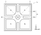
- FIG. 6 is a schematic plan view showing an example of a pixel configuration of an image pickup apparatus having the image pickup device shown in FIG. 24. It is a characteristic figure which showed the relationship between the content of Ga and the carrier mobility in Experimental Example 1 to Experimental Example 6. 6 is a characteristic diagram showing the relationship between the Ga content and the carrier concentration in Experimental Examples 1 to 6. It is sectional drawing which shows an example of the structure of the image sensor which concerns on the modification 4 of this disclosure. It is sectional drawing which shows an example of the structure of the image pickup device which concerns on the modification 5 of this disclosure.
- FIG. 3 is a schematic plan view showing an example of the pixel configuration of the image pickup apparatus having the image pickup device shown in FIG. 30A. It is sectional drawing which shows an example of the structure of the image pickup device which concerns on the modification 7 of this disclosure.
- FIG. 3 is a schematic plan view showing an example of the pixel configuration of the image pickup apparatus having the image pickup device shown in FIG. 31A. It is sectional drawing which shows an example of the structure of the image sensor which concerns on the modification 8 of this disclosure.
- FIG. 3 is a schematic plan view showing an example of the pixel configuration of the image pickup apparatus having the image pickup device shown in FIG. 30A. It is sectional drawing which shows an example of the structure of the image pickup device which concerns on the modification 7 of this disclosure.
- FIG. 3 is a schematic plan view showing an example of the pixel configuration of the image pickup apparatus having the image pickup device
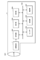
- FIG. 3 is a functional block diagram showing an example of an electronic device (camera) using the imaging device shown in FIG. 33. It is a block diagram which shows another example of the structure of the image pickup apparatus which used the image pickup element shown in FIG. 1 and the like as a pixel.
- FIG. 3 is a block diagram showing another example of the configuration of an electronic device having an imaging device shown in FIG. 33 and the like. It is a block diagram which shows an example of the schematic structure of the body information acquisition system. It is a figure which shows an example of the schematic structure of the endoscopic surgery system. It is a block diagram which shows an example of the functional structure of a camera head and a CCU. It is a block diagram which shows an example of the schematic structure of a vehicle control system. It is explanatory drawing which shows an example of the installation position of the vehicle exterior information detection unit and the image pickup unit.
- Modification 1 (Example in which a protective layer is further provided between the semiconductor layer and the photoelectric conversion layer) 2-2.
- Modification 2 (Example in which a semiconductor layer having a three-layer structure is provided between the lower electrode and the photoelectric conversion layer) 2-3.
- Modification 3 (Example in which a transfer electrode is further provided as a lower electrode) 3.
- Second Embodiment (example of an imaging device having a between the lower electrode and the photoelectric conversion layer, a semiconductor layer composed of two layers having the values of and E VO of a predetermined DerutaEN) 4.
- Modification example 4-1 (Example in which two organic photoelectric conversion parts are laminated on a semiconductor substrate) 4-2.
- Modification 5 (Example in which three organic photoelectric conversion parts are laminated on a semiconductor substrate) 4-3.
- Modification 6 an example of an image sensor that disperses using a color filter) 4-4.
- Modification 7 another example of an image sensor that disperses using a color filter) 4-5.
- Modification 8 Example in which two organic photoelectric conversion parts are laminated on a semiconductor substrate) 5.
- Application example 6. Application example
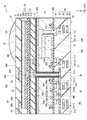
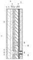
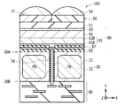
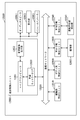
- FIG. 1 shows a cross-sectional configuration of an image pickup device (image pickup device 10) according to the first embodiment of the present disclosure.
- FIG. 2 schematically shows an example of the planar configuration of the image pickup device 10 shown in FIG. 1
- FIG. 1 shows a cross section taken along the line II shown in FIG.
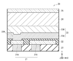
- FIG. 3 is an enlarged schematic representation of an example of the cross-sectional configuration of the main part (organic photoelectric conversion unit 20) of the image sensor 10 shown in FIG.
- the image sensor 10 is arranged in the pixel portion 1A of an image pickup device (for example, image pickup device 1, see FIG.
- CMOS Complementary Metal Oxide Semiconductor
- CMOS Complementary Metal Oxide Semiconductor
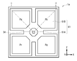
- a pixel unit 1a composed of four unit pixels P arranged in 2 rows ⁇ 2 columns is a repeating unit, and is repeated in an array consisting of a row direction and a column direction. Have been placed.
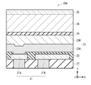
- the image sensor 10 of the present embodiment has a laminated structure between the lower electrode 21 composed of the readout electrode 21A and the storage electrode 21B and the photoelectric conversion layer 24 in the organic photoelectric conversion unit 20 provided on the semiconductor substrate 30.
- the semiconductor layer 23 to be provided is provided.
- the semiconductor layer 23 is composed of, for example, a first semiconductor layer 23A and a second semiconductor layer 23B, and is laminated in this order from the lower electrode 21 side.
- the first semiconductor layer 23A has a value of greater C5s than the value of C5s the second semiconductor layer 23B, the second semiconductor layer 23B, rather than the value of E VO or E VN of the first semiconductor layer 23A It has a large EVO or EVN value.
- the read-out electrode 21A corresponds to a specific example of the "second electrode” of the present disclosure
- the storage electrode 21B corresponds to a specific example of the "first electrode” of the present disclosure
- the first semiconductor layer 23A corresponds to a specific example of the "first layer” of the present disclosure
- the second semiconductor layer 23B corresponds to a specific example of the "second layer” of the present disclosure.
- the image pickup element 10 is, for example, a so-called vertical spectroscopic type in which one organic photoelectric conversion unit 20 and two inorganic photoelectric conversion units 32B and 32R are vertically laminated.
- the organic photoelectric conversion unit 20 is provided on the first surface (back surface) 30A side of the semiconductor substrate 30.
- the inorganic photoelectric conversion units 32B and 32R are embedded and formed in the semiconductor substrate 30, and are laminated in the thickness direction of the semiconductor substrate 30.
- the organic photoelectric conversion unit 20 and the inorganic photoelectric conversion units 32B and 32R selectively detect light in different wavelength ranges and perform photoelectric conversion.
- the organic photoelectric conversion unit 20 acquires a green (G) color signal.
- the inorganic photoelectric conversion units 32B and 32R acquire blue (B) and red (R) color signals, respectively, depending on the difference in absorption coefficient.
- the image sensor 10 can acquire a plurality of types of color signals in one unit pixel P without using a color filter.
- the second surface 30B of the semiconductor substrate 30 for example, floating diffusion (floating diffusion layer) FD1 (region 36B in the semiconductor substrate 30), FD2 (region 37C in the semiconductor substrate 30), FD3 (semiconductor substrate 30) Area 38C), transfer transistors Tr2 and Tr3, amplifier transistor (modulator) AMP, reset transistor RST, and selection transistor SEL are provided.
- the second surface 30B of the semiconductor substrate 30 is further provided with a multilayer wiring layer 40 via a gate insulating layer 33.
- the multilayer wiring layer 40 has, for example, a configuration in which the wiring layers 41, 42, and 43 are laminated in the insulating layer 44.
- a peripheral circuit unit 130 (see FIG. 33) including a logic circuit or the like is provided around the peripheral portion of the semiconductor substrate 30, that is, around the pixel portion 1A.
- the first surface 30A side of the semiconductor substrate 30 is represented as the light incident side S1
- the second surface 30B side is represented as the wiring layer side S2.
- the semiconductor layer 23 and the photoelectric conversion layer 24 formed by using an organic material are laminated in this order from the lower electrode 21 side between the lower electrode 21 and the upper electrode 25 arranged so as to face each other. ing.
- the semiconductor layer 23 as described above, the first semiconductor layer 23A and the second semiconductor layer 23B are laminated in this order from the lower electrode 21 side, and the first semiconductor layer 23A is the value of C5s of the second semiconductor layer 23B. has a value of greater C5s than, the second semiconductor layer 23B has a large value of E VO or E VN than the value of E VO or E VN of the first semiconductor layer 23A.
- the photoelectric conversion layer 24 is composed of a p-type semiconductor and an n-type semiconductor, and has a bulk heterojunction structure in the layer.
- the bulk heterojunction structure is a p / n junction surface formed by mixing p-type semiconductors and n-type semiconductors.
- the organic photoelectric conversion unit 20 further has an insulating layer 22 between the lower electrode 21 and the semiconductor layer 23.
- the insulating layer 22 is provided over the entire surface of the pixel portion 1A, and has an opening 22H on the readout electrode 21A constituting the lower electrode 21, for example.
- the readout electrode 21A is electrically connected to the first semiconductor layer 23A of the semiconductor layer 23 via the opening 22H.
- FIG. 1 shows an example in which the semiconductor layer 23, the photoelectric conversion layer 24, and the upper electrode 25 are separately formed for each image sensor 10, the semiconductor layer 23, the photoelectric conversion layer 24, and the upper electrode 25 are shown.
- it may be provided as a continuous layer common to a plurality of image pickup devices 10.
- an insulating layer 26 and an interlayer insulating layer 27 are provided between the first surface 30A of the semiconductor substrate 30 and the lower electrode 21.
- the insulating layer 26 is composed of a layer having a fixed charge (fixed charge layer) 26A and a dielectric layer 26B having an insulating property.
- the inorganic photoelectric conversion units 32B and 32R have made it possible to disperse light in the vertical direction by utilizing the fact that the wavelength of light absorbed in the semiconductor substrate 30 made of a silicon substrate differs depending on the incident depth of light. Each has a pn junction in a predetermined region of the semiconductor substrate 30.
- a through electrode 34 is provided between the first surface 30A and the second surface 30B of the semiconductor substrate 30.
- the through electrode 34 is electrically connected to the read electrode 21A, and the organic photoelectric conversion unit 20 passes through the through electrode 34 to the gate Gamp of the amplifier transistor AMP and the reset transistor RST (reset transistor) which also serves as the floating diffusion FD1. It is connected to one source / drain region 36B (Tr1rst).
- the electric charge (electrons in this case) generated in the organic photoelectric conversion unit 20 on the first surface 30A side of the semiconductor substrate 30 is transferred to the second surface 30B side of the semiconductor substrate 30 via the through electrode 34. It is possible to transfer the charge well and improve the characteristics.
- the lower end of the through electrode 34 is connected to the connection portion 41A in the wiring layer 41, and the connection portion 41A and the gate Gamp of the amplifier transistor AMP are connected via the lower first contact 45.
- the connecting portion 41A and the floating diffusion FD1 (region 36B) are connected via, for example, a lower second contact 46.
- the upper end of the through electrode 34 is connected to the read electrode 21A via, for example, the pad portion 39A and the upper first contact 39C.
- a protective layer 51 is provided above the organic photoelectric conversion unit 20.
- a wiring 52 and a light-shielding film 53 for electrically connecting the upper electrode 25 and the peripheral circuit portion 130 are provided around the pixel portion 1A.
- an optical member such as a flattening layer (not shown) and an on-chip lens 54 is further arranged.
- the light incident on the organic photoelectric conversion unit 20 from the light incident side S1 is absorbed by the photoelectric conversion layer 24.
- the excitons generated thereby move to the interface between the electron donor and the electron acceptor constituting the photoelectric conversion layer 24, and exciton separation, that is, dissociation into electrons and holes.
- the charges (electrons and holes) generated here differ depending on the diffusion due to the difference in carrier concentration and the internal electric field due to the difference in the work function between the anode (for example, the upper electrode 25) and the cathode (for example, the lower electrode 21). It is carried to the electrode and detected as a photocurrent.
- the transport direction of electrons and holes can also be controlled by applying an electric potential between the lower electrode 21 and the upper electrode 25.
- the organic photoelectric conversion unit 20 is an organic photoelectric conversion element that absorbs green light corresponding to a part or all of a selective wavelength range (for example, 450 nm or more and 650 nm or less) to generate excitons.
- a selective wavelength range for example, 450 nm or more and 650 nm or less
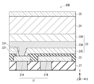
- the lower electrode 21 is composed of, for example, a readout electrode 21A and a storage electrode 21B arranged in parallel on the interlayer insulating layer 27.
- the readout electrode 21A is for transferring the electric charge generated in the photoelectric conversion layer 24 to the floating diffusion FD1, and is, for example, 1 for each pixel unit 1a composed of 4 unit pixels P arranged in 2 rows ⁇ 2 columns. It is provided one by one.
- the read electrode 21A is connected to the floating diffusion FD1 via, for example, the upper first contact 39C, the pad portion 39A, the through electrode 34, the connecting portion 41A, and the lower second contact 46.
- the storage electrode 21B is for storing, for example, electrons in the semiconductor layer 23 as a signal charge among the charges generated in the photoelectric conversion layer 24, and is provided for each unit pixel P.
- the storage electrode 21B is provided for each unit pixel P in a region that faces the light receiving surfaces of the inorganic photoelectric conversion units 32B and 32R formed in the semiconductor substrate 30 and covers these light receiving surfaces.
- the storage electrode 21B is preferably larger than the readout electrode 21A, which allows a large amount of charge to be stored.
- the lower electrode 21 is made of a light-transmitting conductive film, for example, ITO (indium tin oxide).
- ITO indium tin oxide
- a tin oxide (SnO 2 ) -based material to which a dopant is added or a zinc oxide-based material obtained by adding a dopant to zinc oxide (ZnO) may be used.
- the zinc oxide-based material include aluminum zinc oxide (AZO) to which aluminum (Al) is added as a dopant, gallium zinc oxide (GZO) to which gallium (Ga) is added, and indium zinc to which indium (In) is added.
- Oxide (IZO) can be mentioned.
- IGZO, ITZO, CuI, InSbO 4, ZnMgO, CuInO 2, MgIN 2 O 4 may be used CdO or ZnSnO 3, and the like.
- the insulating layer 22 is for electrically separating the storage electrode 21B and the semiconductor layer 23.
- the insulating layer 22 is provided on, for example, the interlayer insulating layer 27 so as to cover the lower electrode 21.
- the insulating layer 22 is provided with an opening 22H above the read-out electrode 21A of the lower electrodes 21, and the read-out electrode 21A and the semiconductor layer 23 are electrically connected via the opening 22H.
- the insulating layer 22 is composed of, for example, a single-layer film made of one of silicon oxide (SiO x ), silicon nitride (SiN x ), silicon oxynitride (SiON), and a laminated film made of two or more. There is.
- the thickness of the insulating layer 22 is, for example, 20 nm or more and 500 nm or less.
- the semiconductor layer 23 is for accumulating the electric charge generated in the photoelectric conversion layer 24.
- the semiconductor layer 23 is provided between the lower electrode 21 and the photoelectric conversion layer 24, and the first semiconductor layer 23A and the second semiconductor layer 23B are laminated in this order from the lower electrode 21 side. It has a laminated structure.
- the first semiconductor layer 23A is provided on the insulating layer 22 that electrically separates the lower electrode 21 and the semiconductor layer 23, and the read electrode 21A is provided in the opening 22H provided on the read electrode 21A. Is directly electrically connected to.
- the second semiconductor layer 23B is provided between the first semiconductor layer 23A and the photoelectric conversion layer 24.
- the semiconductor layer 23 can be formed by using, for example, an oxide semiconductor material.
- an oxide semiconductor material since electrons are used as signal charges among the charges generated in the photoelectric conversion layer 24, the semiconductor layer 23 can be formed by using an n-type oxide semiconductor material.
- the first semiconductor layer 23A is for preventing the electric charge accumulated in the semiconductor layer 23 from being trapped at the interface with the insulating layer 22 and efficiently transferring the electric charge to the read electrode 21A.
- the second semiconductor layer 23B is for preventing the desorption of oxygen on the surface of the first semiconductor layer 23A and preventing the electric charge generated in the photoelectric conversion layer 24 from being trapped at the interface with the photoelectric conversion layer 24. .. Therefore, the first semiconductor layer 23A can be formed by including an oxide semiconductor material having a value of C5s larger than the value of C5s of the second semiconductor layer 23B.
- the second semiconductor layer 23B can be formed by including an oxide semiconductor material having an EVO value larger than the EVO value of the first semiconductor layer 23A.
- the first semiconductor layer 23A can be formed by including an oxide semiconductor material satisfying C5s> 50%, more preferably an oxide semiconductor material satisfying C5s> 80%.
- the second semiconductor layer 23B is an oxide semiconductor material that satisfies E VO> 2.3 eV, more preferably, may be formed to include an oxide semiconductor material that satisfies E VO> 2.8 eV.
- C5s is a value indicating the contribution ratio of the 5s orbital to the bottom of the conduction band (Conduction Band Minimum: CBM).
- CBM Conduction Band Minimum
- the CMB of an oxide semiconductor is made by mixing the s orbitals of each metal element. Among them, when the ratio of the 5s orbitals (s orbitals of cadmium (Cd), indium (In) and tin (Sn)) having the largest spatial spread is large, the number of transfer traps decreases.
- C5s can be obtained from, for example, first-principles calculation.
- a model is created by the calculation method used when calculating the oxygen defect generation energy described later.
- the number of oxygen atoms is modeled by the number calculated from the valence without decreasing, as in the method of calculating the oxygen defect generation energy.
- From the electronic state obtained when calculating the model the orbital corresponding to CBM is specified.
- the CBM is the smallest energy orbit in which an electron is unoccupied.
- the contribution ratio of the 5s orbitals (s orbitals of Cd, In and Sn) to the CBM is determined.
- VASP Vienna Ab Initio Simulation Package
- PROCAR Partial Density Of States
- EVO refers to the average value of oxygen deficiency generation energy possessed by a plurality of types of metal atoms. It can be said that the higher the value of the oxygen deficiency generation energy, the more difficult it is for oxygen atoms to be desorbed, and the more difficult it is for oxygen atoms, oxygen molecules, or other atoms or molecules to be taken in, so that it is stable.
- the oxygen deficiency generation energy EVO can be obtained from, for example, first-principles calculation, and is calculated from the following mathematical formula (1). Specifically, first, an amorphous structure having the same ratio of atoms as the target metal element composition and the corresponding oxygen number is created. As the oxygen number, a general metal ion valence is used. That is, zinc (Zn) and Cd are +2 valence, gallium (Ga) and In are +3 valence, and germanium (Ge) and Sn are +4 valence. Oxygen ion is -2 valent and contains a few neutral oxygen. Further, it is desirable that the total number of atoms is 80 or more.
- the first semiconductor layer 23A can be formed as, for example, an amorphous layer. As a result, it is possible to prevent an increase in the carrier density of the first semiconductor layer 23A and realize a low carrier concentration. Further, as compared with the case where the first semiconductor layer 23A is formed as a crystal layer, the generation of dangling bonds at the grain boundaries in the first semiconductor layer 23A and the interface with the insulating layer 22 is suppressed, and the trap is lower. Can be transformed into.
- the film quality of the second semiconductor layer 23B is not particularly limited, and may be a crystal layer or may be formed as an amorphous layer.
- the amorphous layer and the crystal layer can be judged by the presence or absence of haloing of the fast Fourier transform (FFT) image of the transmission electron microscope (TEM) image.
- FFT fast Fourier transform
- TEM transmission electron microscope
- a bright and dark striped image corresponding to both intervals of the lattice appears on the crystal layer due to the interference between the diffracted wave and the transmitted wave from the lattice surface having the crystal. This is called a plaid.
- no plaid is confirmed.
- FFTing the TEM image in two dimensions the patterns shown in FIGS. 4 and 5 can be confirmed.
- the crystal layer as shown in FIG.
- a speckled pattern extending in one direction corresponding to the period of the plaid can be confirmed.
- a broad ring-shaped pattern can be confirmed. This is halo ring.
- FIGS. 4 and 5 show the correspondence between the patterns of the crystal layer and the amorphous layer shown in FIGS. 4 and 5, respectively, and their strength profiles.
- the unit pixel P is 30 pixels in the horizontal direction of the paper surface for the FFT pattern of the rectangular square region of the thickness ⁇ width 45 nm of each of the crystal layer and the amorphous layer (FIGS. 4 and 5).
- Area X) is the actual intensity profile (histogram) integrated.
- the intensity profile of the crystal layer three peaks corresponding to the three filled spots can be confirmed in FIG. 4, whereas the intensity profile of the amorphous layer is broad.
- Examples of the constituent materials of the semiconductor layer 23 include ITO, IZO, IGO, ZTO, IGZO (In—Ga—Zn—O-based oxide semiconductor), and GZTO (Ga).
- -Zn-Sn-O-based oxide semiconductors ITZO (In-Sn-Zn-O-based oxide semiconductors), IGZTO (In-Ga-Zn-Sn-O-based oxide semiconductors), and the like.
- IGTO In—Ga—Sn—O-based oxide semiconductor
- the semiconductor layer 23 may contain, for example, silicon (Si), aluminum (Al), titanium (Ti), molybdenum (Mo), carbon (C), cadmium (Cd) and the like.
- the first semiconductor layer 23A is preferably formed by using ITO, IZO, indium-rich ITZO (cation ratio In> 50%), IGO or tin-rich SnZNO (cation ratio Sn> 50%). More specifically, the first semiconductor layer 23A can be formed by using , for example, In 2 O 3 (ITO) to which 10 wt% of SnO 2 is added or In 2 O 3 (IZO) to which 10 wt% of ZnO is added. preferable. As the second semiconductor layer 23B, it is preferable to use IGZO, IGZTO, ZTO, GZTO or IGTO.
- ZTO having a cation ratio of Zn> 60%
- In + Sn having a cation ratio of 50% or less and a ratio of Ga + An.
- Is preferably formed using IGZTO of 50% or more.
- C5s in the above material can be adjusted as follows. First, a candidate composition (cation ratio) is determined, and a sufficient number of oxygens that become neutral when the cation is ionized are added. At this time, the number of cations is preferably about 30 to 40 or more.
- the valence of Sn is +4, the valence of In is +3, the valence of Ga is +3, the valence of Zn is +2, and the valence of O is -2.
- the value of C5s of the target composition can be calculated.
- the value of C5s tends to increase as the number of 5s elements such as In and Sn increases.
- C5s> satisfy 80%, such as ITO the first semiconductor layer 23A using a (In 2 O 3 having a SnO 2 was added 10 wt%), satisfies the E VO> 2.8V, for example, IGZO (an In: It represents the elemental composition in the semiconductor layer 23 when the second semiconductor layer 23B is formed using Ga: Zn 1: 1: 1).
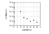
- the charges accumulated in the semiconductor layer 23 from the photoelectric conversion layer 24 are as shown in FIG. In addition, it is trapped in the 4s orbit of Ga, and its movement to the read electrode 21A is hindered.
- the thickness of the first semiconductor layer 23A is, for example, 2 nm or more and 10 nm or less.
- the thickness of the second semiconductor layer 23B is, for example, 15 nm or more and 100 nm or less.
- the ratio (t2 / t1) of the thickness (t2) of the second semiconductor layer 23B to the thickness (t1) of the first semiconductor layer 23A is preferably 4 or more and 8 or less.
- Table 1 shows the films of the first semiconductor layer 23A and the second semiconductor layer 23B calculated from the ID- V GS curves obtained by manufacturing a simple TFT (Thin-Film-Transistor) element and evaluating the TFT. This is a summary of the on-voltages of the thickness ratio (t2 / t1).
- the TFT element is formed by forming a SiO 2 film, a first semiconductor layer 23A, and a second semiconductor layer 23B in this order on a silicon substrate, and providing a source electrode and a drain electrode on the second semiconductor layer 23B.
- the first semiconductor layer 23A is an amorphous layer as described above, it is possible to realize a low carrier concentration while preventing an increase in the carrier density of the semiconductor layer 23.
- the constituent materials of the first semiconductor layer 23A and the second semiconductor layer 23B a nitride semiconductor material or an oxynitride semiconductor material can be used in addition to the oxide semiconductor material.
- the nitrogen deficiency generation energy EVN is used as an index instead of the oxygen deficiency generation energy EVO. That is, the second semiconductor layer 23B may be formed to include a nitride semiconductor material having a large value of E VN than the value of E VN of the first semiconductor layer 23A (eg, E VN> 2.3 eV) .
- the nitrogen deficiency generation energy EVN can be similarly calculated by replacing the oxygen atom with the nitrogen atom in the above-mentioned calculation method of the oxygen deficiency generation energy EVO.
- the photoelectric conversion layer 24 is for converting light energy into electrical energy.
- the photoelectric conversion layer 24 is composed of, for example, two or more types of organic materials (p-type semiconductor materials or n-type semiconductor materials) that function as p-type semiconductors or n-type semiconductors, respectively.
- the photoelectric conversion layer 24 has a bonding surface (p / n bonding surface) between the p-type semiconductor material and the n-type semiconductor material in the layer.
- the p-type semiconductor functions relatively as an electron donor (donor), and the n-type semiconductor functions relatively as an electron acceptor (acceptor).
- the photoelectric conversion layer 24 provides a place where excitons generated when light is absorbed are separated into electrons and holes. Specifically, the interface between the electron donor and the electron acceptor (p /). At the n junction surface), excitons separate into electrons and holes.
- the photoelectric conversion layer 24 includes, in addition to the p-type semiconductor material and the n-type semiconductor material, an organic material that photoelectrically converts light in a predetermined wavelength range while transmitting light in another wavelength range, that is, a so-called dye material. It may have been done.
- the photoelectric conversion layer 24 is formed using three types of organic materials, a p-type semiconductor material, an n-type semiconductor material, and a dye material, the p-type semiconductor material and the n-type semiconductor material are in the visible region (for example, from 450 nm). It is preferable that the material has light transmission at 800 nm).
- the thickness of the photoelectric conversion layer 24 is, for example, 50 nm or more and 500 nm or less.
- the photoelectric conversion layer 24 of the present embodiment contains an organic material and has absorption between visible light and near infrared light.
- the organic material constituting the photoelectric conversion layer 24 include quinacridone derivatives, naphthalene derivatives, anthracene derivatives, phenanthrene derivatives, tetracene derivatives, pyrene derivatives, perylene derivatives and fluoranthene derivatives.
- the photoelectric conversion layer 24 is composed of a combination of two or more of the above organic materials.
- the organic material functions as a p-type semiconductor or an n-type semiconductor depending on the combination thereof.
- the organic material constituting the photoelectric conversion layer 24 is not particularly limited.
- polymers such as phenylene vinylene, fluorene, carbazole, indole, pyrrole, pyrrole, picolin, thiophene, acetylene and diacetylene or derivatives thereof can be used.
- metal complex dyes cyanine dyes, merocyanine dyes, phenylxanthene dyes, triphenylmethane dyes, rodacyanine dyes, xanthene dyes, macrocyclic azaanulene dyes, azulene dyes, naphthoquinone dyes, anthraquinone dyes.
- Pyrene and other condensed polycyclic aromatic compounds chain compounds fused with aromatic rings or heterocyclic compounds, and two nitrogen-containing heterocycles such as quinoline, benzothiazole, and benzoxanthene having a squarylium group and a croconitecmethine group as bonding chains.
- a cyanine-based dye or the like bonded by a squarylium group and a croconitecmethine group can be used.
- the metal complex dye include a dithiol metal complex dye, a metal phthalocyanine dye, a metal porphyrin dye, and a ruthenium complex dye. Of these, ruthenium complex dyes are particularly preferable, but are not limited to the above.
- the upper electrode 25 is made of a conductive film having light transmission like the lower electrode 21, and is made of, for example, ITO.
- ITO a tin oxide (SnO 2 ) -based material to which a dopant is added or a zinc oxide-based material obtained by adding a dopant to zinc oxide (ZnO) is used. May be good.
- the zinc oxide-based material include aluminum zinc oxide (AZO) to which aluminum (Al) is added as a dopant, gallium zinc oxide (GZO) to which gallium (Ga) is added, and indium zinc to which indium (In) is added.
- Oxide (IZO) can be mentioned.
- the upper electrode 25 may be separated for each unit pixel P, or may be formed as an electrode common to each unit pixel P.
- the thickness of the upper electrode 25 is, for example, 10 nm or more and 200 nm or less.
- the photoelectric conversion layer 24 and the lower electrode 21 are provided between the photoelectric conversion layer 24 and the lower electrode 21 (for example, between the semiconductor layer 23 and the photoelectric conversion layer 24) and between the photoelectric conversion layer 24 and the upper electrode 25.
- the semiconductor layer 23, the buffer layer also serving as an electron blocking film, the photoelectric conversion layer 24, the buffer layer also serving as a hole blocking film, the work function adjusting layer, and the like may be laminated in this order from the lower electrode 21 side.
- the photoelectric conversion layer 24 may have, for example, a pin bulk heterostructure in which a p-type blocking layer, a layer (i layer) containing a p-type semiconductor and an n-type semiconductor, and an n-type blocking layer are laminated.
- the insulating layer 26 covers the first surface 30A of the semiconductor substrate 30, reduces the interface state with the semiconductor substrate 30, and suppresses the generation of dark current from the interface with the semiconductor substrate 30. Further, the insulating layer 26 extends from the first surface 30A of the semiconductor substrate 30 to the side surface of the opening 34H (see FIG. 14) in which the through electrodes 34 penetrating the second surface 30B are formed.
- the insulating layer 26 has, for example, a laminated structure of a fixed charge layer 26A and a dielectric layer 26B.
- the fixed charge layer 26A may be a film having a positive fixed charge or a film having a negative fixed charge.
- the constituent material of the fixed charge layer 26A it is preferable to use a semiconductor material or a conductive material having a bandgap wider than that of the semiconductor substrate 30. As a result, it is possible to suppress the generation of dark current at the interface of the semiconductor substrate 30.
- the constituent materials of the fixed charge layer 26A include hafnium oxide (HfO x ), aluminum oxide (AlO x ), zirconium oxide (ZrO x ), tantalum oxide (TaO x ), titanium oxide (TIO x ), and lanthanum oxide (Tio x).
- the dielectric layer 26B is for preventing the reflection of light caused by the difference in refractive index between the semiconductor substrate 30 and the interlayer insulating layer 27.
- the constituent material of the dielectric layer 26B is preferably a material having a refractive index between the refractive index of the semiconductor substrate 30 and the refractive index of the interlayer insulating layer 27.
- Examples of the constituent material of the dielectric layer 26B include silicon oxide, TEOS, silicon nitride, silicon oxynitride (SiON) and the like.
- the interlayer insulating layer 27 is composed of, for example, a single-layer film made of one of silicon oxide, silicon nitride, silicon oxynitride, and the like, or a laminated film made of two or more of these.
- a shield electrode 28 is provided on the interlayer insulating layer 27 together with a lower electrode 21.
- the shield electrode 28 is for preventing capacitive coupling between adjacent pixel units 1a.
- the shield electrode 28 is provided and fixed around a pixel unit 1a composed of four unit pixels P arranged in 2 rows ⁇ 2 columns. An electric potential is applied.
- the shield electrode 28 further extends in the pixel unit 1a between unit pixels P adjacent to each other in the row direction (Z-axis direction) and the column direction (X-axis direction).
- the semiconductor substrate 30 is composed of, for example, an n-type silicon (Si) substrate, and has a p-well 31 in a predetermined region.
- the inorganic photoelectric conversion units 32B and 32R are each composed of a photodiode (PD) having a pn junction in a predetermined region of the semiconductor substrate 30, and the wavelength of light absorbed by the Si substrate according to the incident depth of light is set. It is possible to disperse light in the vertical direction by utilizing different things.
- the inorganic photoelectric conversion unit 32B selectively detects blue light and accumulates a signal charge corresponding to blue light, and is installed at a depth at which blue light can be efficiently photoelectrically converted.
- the inorganic photoelectric conversion unit 32R selectively detects red light and accumulates a signal charge corresponding to red, and is installed at a depth at which red light can be efficiently photoelectrically converted.
- Blue (B) is, for example, a color corresponding to a wavelength range of 450 nm or more and 495 nm or less
- red (R) is a color corresponding to, for example, a wavelength range of 620 nm or more and 750 nm or less. It suffices that the inorganic photoelectric conversion units 32B and 32R can detect light in a part or all of each wavelength range, respectively.
- the inorganic photoelectric conversion unit 32B includes, for example, a p + region serving as a hole storage layer and an n region serving as an electron storage layer.
- the inorganic photoelectric conversion unit 32R has, for example, a p + region serving as a hole storage layer and an n region serving as an electron storage layer (having a pn-p laminated structure).
- the n region of the inorganic photoelectric conversion unit 32B is connected to the vertical transfer transistor Tr2.
- the p + region of the inorganic photoelectric conversion unit 32B is bent along the transfer transistor Tr2 and is connected to the p + region of the inorganic photoelectric conversion unit 32R.
- the gate insulating layer 33 is composed of, for example, a single-layer film made of one of silicon oxide, silicon nitride, silicon oxynitride, and the like, or a laminated film made of two or more of these.
- the through electrode 34 is provided between the first surface 30A and the second surface 30B of the semiconductor substrate 30, and has a function as a connector between the organic photoelectric conversion unit 20 and the gate Gamp and the floating diffusion FD1 of the amplifier transistor AMP. , It serves as a transmission path for the electric charge generated in the organic photoelectric conversion unit 20.
- the reset gate Grst of the reset transistor RST is arranged next to the floating diffusion FD1 (one source / drain region 36B of the reset transistor RST). As a result, the electric charge accumulated in the floating diffusion FD1 can be reset by the reset transistor RST.
- the pad portions 39A and 39B, the upper first contact 39C, the upper second contact 39D, the lower first contact 45, the lower second contact 46 and the wiring 52 are made of a doped silicon material such as PDAS (Phosphorus Doped Amorphous Silicon).
- PDAS Phosphorus Doped Amorphous Silicon
- it can be formed using a metal material such as aluminum (Al), tungsten (W), titanium (Ti), cobalt (Co), hafnium (Hf) and tantalum (Ta).
- the protective layer 51 and the on-chip lens 54 are made of a light-transmitting material, for example, a single-layer film made of silicon oxide, silicon nitride, silicon oxynitride, or the like, or two of them. It is composed of the above-mentioned laminated film.
- the thickness of the protective layer 51 is, for example, 100 nm or more and 30,000 nm or less.
- the light-shielding film 53 is provided in the protective layer 51 together with the wiring 52 so as to cover the region of the readout electrode 21A which is in direct contact with the semiconductor layer 23 without covering at least the storage electrode 21B.
- the light-shielding film 53 can be formed by using, for example, tungsten (W), aluminum (Al), an alloy of Al and copper (Cu), or the like.
- FIG. 11 is an equivalent circuit diagram of the image pickup device 10 shown in FIG.
- FIG. 12 schematically shows the arrangement of the lower electrode 21 of the image pickup device 10 shown in FIG. 1 and the transistors constituting the control unit.
- the reset transistor RST (reset transistor TR1rst) is for resetting the electric charge transferred from the organic photoelectric conversion unit 20 to the floating diffusion FD1, and is composed of, for example, a MOS transistor.
- the reset transistor TR1rst is composed of a reset gate Grst, a channel forming region 36A, and source / drain regions 36B and 36C.
- the reset gate Grst is connected to the reset line RST1, and one source / drain region 36B of the reset transistor TR1rst also serves as a floating diffusion FD1.
- the other source / drain region 36C constituting the reset transistor TR1rst is connected to the power supply line VDD.
- the amplifier transistor AMP is a modulation element that modulates the amount of electric charge generated by the organic photoelectric conversion unit 20 into a voltage, and is composed of, for example, a MOS transistor. Specifically, the amplifier transistor AMP is composed of a gate Gamp, a channel forming region 35A, and source / drain regions 35B and 35C.
- the gate Gamp is connected to one source / drain region 36B (floating diffusion FD1) of the read electrode 21A and the reset transistor TR1rst via the lower first contact 45, the connecting portion 41A, the lower second contact 46, the through electrode 34, and the like. Has been done. Further, one source / drain region 35B shares an region with the other source / drain region 36C constituting the reset transistor TR1rst, and is connected to the power supply line VDD.
- the selection transistor SEL selection transistor TR1sel
- the selection transistor SEL is composed of a gate Gsel, a channel formation region 34A, and source / drain regions 34B and 34C.
- the gate Gsel is connected to the selection line SEL1.
- One source / drain region 34B shares an area with the other source / drain region 35C constituting the amplifier transistor AMP, and the other source / drain region 34C is connected to the signal line (data output line) VSL1. Has been done.
- the transfer transistor TR2 (transfer transistor TR2trs) is for transferring the signal charge corresponding to the blue color generated and accumulated in the inorganic photoelectric conversion unit 32B to the floating diffusion FD2. Since the inorganic photoelectric conversion unit 32B is formed at a position deep from the second surface 30B of the semiconductor substrate 30, it is preferable that the transfer transistor TR2trs of the inorganic photoelectric conversion unit 32B is composed of a vertical transistor.
- the transfer transistor TR2trs is connected to the transfer gate line TG2.
- a floating diffusion FD2 is provided in a region 37C near the gate Gtrs2 of the transfer transistor TR2trs. The charge accumulated in the inorganic photoelectric conversion unit 32B is read out to the floating diffusion FD2 via a transfer channel formed along the gate Gtrs2.
- the transfer transistor TR3 (transfer transistor TR3trs) is for transferring the signal charge corresponding to the accumulated red color generated in the inorganic photoelectric conversion unit 32R to the floating diffusion FD3, and is composed of, for example, a MOS transistor. ..
- the transfer transistor TR3trs is connected to the transfer gate line TG3.
- a floating diffusion FD3 is provided in the region 38C near the gate Gtrs3 of the transfer transistor TR3trs.
- the charge accumulated in the inorganic photoelectric conversion unit 32R is read out to the floating diffusion FD3 via a transfer channel formed along the gate Gtrs3.
- a reset transistor TR2rst On the second surface 30B side of the semiconductor substrate 30, a reset transistor TR2rst, an amplifier transistor TR2amp, and a selection transistor TR2sel that form a control unit of the inorganic photoelectric conversion unit 32B are further provided. Further, a reset transistor TR3rst, an amplifier transistor TR3amp, and a selection transistor TR3sel, which form a control unit of the inorganic photoelectric conversion unit 32R, are provided.
- the reset transistor TR2rst is composed of a gate, a channel forming region, and a source / drain region.
- the gate of the reset transistor TR2rst is connected to the reset line RST2, and one source / drain region of the reset transistor TR2rst is connected to the power supply line VDD.
- the other source / drain region of the reset transistor TR2rst also serves as a floating diffusion FD2.
- the amplifier transistor TR2amp is composed of a gate, a channel forming region, and a source / drain region.
- the gate is connected to the other source / drain region (floating diffusion FD2) of the reset transistor TR2rst.
- One source / drain region constituting the amplifier transistor TR2amp shares an region with one source / drain region constituting the reset transistor TR2rst, and is connected to the power supply line VDD.
- the selection transistor TR2sel is composed of a gate, a channel forming region, and a source / drain region.
- the gate is connected to the selection line SEL2.
- One source / drain region constituting the selection transistor TR2sel shares an region with the other source / drain region constituting the amplifier transistor TR2amp.
- the other source / drain region constituting the selection transistor TR2sel is connected to the signal line (data output line) VSL2.
- the reset transistor TR3rst is composed of a gate, a channel forming region, and a source / drain region.
- the gate of the reset transistor TR3rst is connected to the reset line RST3, and one source / drain region constituting the reset transistor TR3rst is connected to the power supply line VDD.
- the other source / drain region constituting the reset transistor TR3rst also serves as a floating diffusion FD3.
- the amplifier transistor TR3amp is composed of a gate, a channel forming region, and a source / drain region.
- the gate is connected to the other source / drain region (floating diffusion FD3) constituting the reset transistor TR3rst.
- One source / drain region constituting the amplifier transistor TR3amp shares an region with one source / drain region constituting the reset transistor TR3rst, and is connected to the power supply line VDD.
- the selection transistor TR3sel is composed of a gate, a channel forming region, and a source / drain region.
- the gate is connected to the selection line SEL3.
- One source / drain region constituting the selection transistor TR3sel shares an region with the other source / drain region constituting the amplifier transistor TR3amp.
- the other source / drain region constituting the selection transistor TR3sel is connected to the signal line (data output line) VSL3.
- the reset lines RST1, RST2, RST3, selection lines SEL1, SEL2, SEL3, and transfer gate lines TG2, TG3 are each connected to a vertical drive circuit constituting the drive circuit.
- the signal lines (data output lines) VSL1, VSL2, and VSL3 are connected to the column signal processing circuit 113 constituting the drive circuit.
- the image sensor 10 of the present embodiment can be manufactured, for example, as follows.
- FIG. 13 to 18 show the manufacturing method of the image sensor 10 in the order of processes.
- a p-well 31 is formed in the semiconductor substrate 30, and for example, n-type inorganic photoelectric conversion units 32B and 32R are formed in the p-well 31.
- a p + region is formed in the vicinity of the first surface 30A of the semiconductor substrate 30.
- the second surface 30B of the semiconductor substrate 30 is formed with an n + region to be, for example, floating diffusion FD1 to FD3, and then the gate insulating layer 33, the transfer transistor Tr2, and the transfer transistor Tr3 are selected.
- a gate wiring layer 47 including each gate of the transistor SEL, the amplifier transistor AMP, and the reset transistor RST is formed.
- the transfer transistor Tr2, the transfer transistor Tr3, the selection transistor SEL, the amplifier transistor AMP, and the reset transistor RST are formed.
- a multilayer wiring layer 40 composed of wiring layers 41 to 43 including a lower first contact 45, a lower second contact 46, and a connecting portion 41A and an insulating layer 44 is formed on the second surface 30B of the semiconductor substrate 30.
- an SOI (Silicon on Insulator) substrate in which a semiconductor substrate 30, an embedded oxide film (not shown), and a holding substrate (not shown) are laminated is used.
- the embedded oxide film and the holding substrate are bonded to the first surface 30A of the semiconductor substrate 30. After ion implantation, annealing is performed.
- a support substrate (not shown) or another semiconductor substrate is bonded onto the multilayer wiring layer 40 provided on the second surface 30B side of the semiconductor substrate 30, and the semiconductor substrate 30 is turned upside down. Subsequently, the semiconductor substrate 30 is separated from the embedded oxide film and the holding substrate of the SOI substrate to expose the first surface 30A of the semiconductor substrate 30.
- CMOS processes such as ion implantation and CVD (Chemical Vapor Deposition) methods.
- the semiconductor substrate 30 is processed from the first surface 30A side by, for example, dry etching to form, for example, an annular opening 34H.
- the depth of the opening 34H penetrates from the first surface 30A to the second surface 30B of the semiconductor substrate 30, and reaches, for example, the connection portion 41A.
- a negative fixed charge layer 26A and a dielectric layer 26B are sequentially formed on the first surface 30A and the side surface of the opening 34H of the semiconductor substrate 30.
- the fixed charge layer 26A can be formed, for example, by forming a hafnium oxide film or an aluminum oxide film using an atomic layer deposition method (ALD method).
- the dielectric layer 26B can be formed, for example, by forming a silicon oxide film using a plasma CVD method.
- pad portions 39A and 39B in which a barrier metal made of a laminated film of titanium and titanium nitride (Ti / TiN film) and a tungsten film are laminated are formed at predetermined positions on the dielectric layer 26B. ..
- the pad portions 39A and 39B can be used as a light-shielding film.
- the interlayer insulating layer 27 is formed on the dielectric layer 26B and the pad portions 39A and 39B, and the surface of the interlayer insulating layer 27 is flattened by using a CMP (Chemical Mechanical Polishing) method.
- a conductive material such as Al is embedded in the openings 27H1,27H2, and the upper first contact 39C is formed. And the upper second contact 39D is formed.
- a conductive film 21x is formed on the interlayer insulating layer 27 by, for example, a sputtering method, and then patterning is performed using a photolithography technique. Specifically, after forming a photoresist PR at a predetermined position of the conductive film 21x, the conductive film 21x is processed by dry etching or wet etching. After that, by removing the photoresist PR, the readout electrode 21A and the storage electrode 21B are formed as shown in FIG.
- a semiconductor layer 23 composed of an insulating layer 22, a first semiconductor layer 23A and a second semiconductor layer 23B, a photoelectric conversion layer 24, and an upper electrode 25 are formed.
- the insulating layer 22 for example, a silicon oxide film is formed by using the ALD method, and then the surface of the insulating layer 22 is flattened by using the CMP method. Then, the opening 22H is formed on the readout electrode 21A by, for example, wet etching.
- the semiconductor layer 23 can be formed, for example, by using a sputtering method.
- the photoelectric conversion layer 24 is formed, for example, by using a vacuum vapor deposition method.
- the upper electrode 25 is formed by, for example, a sputtering method. Finally, the protective layer 51, the wiring 52, the light-shielding film 53, and the on-chip lens 54 are arranged on the upper electrode 25. As a result, the image sensor 10 shown in FIG. 1 is completed.
- a buffer layer that also serves as an electron blocking film As described above, between the semiconductor layer 23 and the photoelectric conversion layer 24 and between the photoelectric conversion layer 24 and the upper electrode 25, a buffer layer that also serves as an electron blocking film, a buffer layer that also serves as a hole blocking film, or When forming other layers containing an organic material such as a work function adjusting layer, it is desirable to form each layer continuously (in a vacuum integrated process) in a vacuum process. Further, the film forming method of the photoelectric conversion layer 24 is not necessarily limited to the method using the vacuum vapor deposition method, and for example, a spin coating technique, a printing technique, or the like may be used.
- a vacuum vapor deposition method a reactive vapor deposition method, an electron beam vapor deposition method, an ion plating method, etc.
- CVD method Various chemical vapor deposition methods (CVD method) including physical vapor deposition method (PVD method), pyrosol method, thermal decomposition method for organic metal compounds, spray method, dip method, MOCVD method, electroless plating method And the electrolytic plating method can be mentioned.
- the organic photoelectric conversion unit 20 is connected to the gate Gamp of the amplifier transistor AMP and the floating diffusion FD1 via the through electrode 34. Therefore, the electrons of the excitons generated by the organic photoelectric conversion unit 20 are taken out from the lower electrode 21 side, transferred to the second surface 30S2 side of the semiconductor substrate 30 via the through electrode 34, and accumulated in the floating diffusion FD1. Will be done.
- the amplifier transistor AMP modulates the amount of charge generated in the organic photoelectric conversion unit 20 into a voltage.
- the reset gate Grst of the reset transistor RST is arranged next to the floating diffusion FD1. As a result, the electric charge accumulated in the floating diffusion FD1 is reset by the reset transistor RST.
- the organic photoelectric conversion unit 20 is connected not only to the amplifier transistor AMP but also to the floating diffusion FD1 via the through electrode 34, the electric charge accumulated in the floating diffusion FD1 can be easily reset by the reset transistor RST. It will be possible.
- FIG. 19 shows an operation example of the image sensor 10.
- A shows the potential at the storage electrode 21B
- B shows the potential at the floating diffusion FD1 (reading electrode 21A)
- C shows the potential at the gate (Gsel) of the reset transistor TR1rst. Is.
- a voltage is individually applied to the readout electrode 21A and the storage electrode 21B.
- the potential V1 is applied to the readout electrode 21A from the drive circuit and the potential V2 is applied to the storage electrode 21B during the storage period.
- the potentials V1 and V2 are set to V2> V1.
- the electric charge (signal charge; electron) generated by the photoelectric conversion is attracted to the storage electrode 21B and accumulated in the region of the semiconductor layer 23 facing the storage electrode 21B (storage period).
- the potential in the region of the semiconductor layer 23 facing the storage electrode 21B becomes a more negative value with the passage of time of photoelectric conversion.
- the holes are sent from the upper electrode 25 to the drive circuit.
- the image sensor 10 is reset at a later stage of the storage period. Specifically, at timing t1, the scanning unit changes the voltage of the reset signal RST from a low level to a high level. As a result, in the unit pixel P, the reset transistor TR1rst is turned on, and as a result, the voltage of the floating diffusion FD1 is set to the power supply voltage, and the voltage of the floating diffusion FD1 is reset (reset period).
- the electric charge is read out. Specifically, at the timing t2, the potential V3 is applied to the reading electrode 21A from the drive circuit, and the potential V4 is applied to the storage electrode 21B. Here, the potentials V3 and V4 are set to V3 ⁇ V4. As a result, the electric charge accumulated in the region corresponding to the storage electrode 21B is read out from the read electrode 21A to the floating diffusion FD1. That is, the electric charge accumulated in the semiconductor layer 23 is read out to the control unit (transfer period).
- the potential V1 is applied to the read electrode 21A from the drive circuit again, and the potential V2 is applied to the storage electrode 21B.
- the electric charge generated by the photoelectric conversion is attracted to the storage electrode 21B and accumulated in the region of the photoelectric conversion layer 24 facing the storage electrode 21B (accumulation period).
- the inorganic photoelectric conversion unit 32R electrons corresponding to the incident red light are accumulated in the n region of the inorganic photoelectric conversion unit 32R, and the accumulated electrons are transferred to the floating diffusion FD3 by the transfer transistor Tr3.
- the image sensor 10 of the present embodiment has the first semiconductor layer 23A and the first semiconductor layer 23A from the lower electrode 21 side between the lower electrode 21 composed of the readout electrode 21A and the storage electrode 21B and the photoelectric conversion layer 24.
- the semiconductor layer 23 in which the second semiconductor layer 23B is laminated in this order is provided.
- the first semiconductor layer 23A has a value of greater C5s than the value of C5s the second semiconductor layer 23B, the second semiconductor layer 23B, rather than the value of E VO or E VN of the first semiconductor layer 23A It has a large EVO or EVN value.
- the transport characteristics of the electric charges accumulated in the semiconductor layer 23 above the storage electrode 21B in the in-plane direction are improved. Further, the desorption of oxygen or nitrogen from the first semiconductor layer 23A is reduced, and the occurrence of traps at the interface between the semiconductor layer 23 and the photoelectric conversion layer 24 is reduced. This will be described below.
- a stacked image sensor in which a plurality of photoelectric conversion units are vertically laminated has been developed.
- a laminated image sensor for example, two inorganic photoelectric conversion units each made of a photodiode (PD) are laminated on a silicon (Si) substrate, and an organic having a photoelectric conversion layer containing an organic material above the Si substrate. It has a configuration in which a photoelectric conversion unit is provided.
- the stacked image sensor requires a structure that accumulates and transfers the signal charge generated in each photoelectric conversion unit.
- the organic photoelectric conversion unit for example, the inorganic photoelectric conversion unit side of the pair of electrodes in which the photoelectric conversion layers are arranged to face each other is composed of two electrodes, a first electrode and a charge storage electrode. , The signal charge generated in the photoelectric conversion layer can be accumulated.
- the signal charge is temporarily stored above the charge storage electrode and then transferred to the floating diffusion FD in the Si substrate.
- the charge storage portion is completely depleted at the start of exposure, and the charge can be erased.
- an imaging element having a plurality of electrodes on the inorganic photoelectric conversion unit side as described above, indium-gallium-is sandwiched between the first electrode including the charge storage electrode and the photoelectric conversion layer.
- An imaging device in which the photoresponsiveness is improved by providing a composite oxide layer made of zinc composite oxide (IGZO) is disclosed.
- IGZO zinc composite oxide
- electrons are likely to be desorbed by a trap contained at the interface between the insulating film covering the charge storage electrode and the composite oxide layer, which causes transfer noise and contributes to deterioration of afterimage characteristics. ing.
- the first semiconductor layer 23A and the second semiconductor layer 23B are placed on the lower electrode 21 side between the lower electrode 21 composed of the readout electrode 21A and the storage electrode 21B and the photoelectric conversion layer 24.
- the semiconductor layers 23 laminated in this order are provided.
- the first semiconductor layer 23A has a value of C5s larger than the value of C5s of the second semiconductor layer 23B, whereby the surface of the charge accumulated in the semiconductor layer 23 above the storage electrode 21B. Inward transport characteristics are improved.
- the second semiconductor layer 23B has an EVO or EVN value larger than the EVO or EVN value of the first semiconductor layer 23A, whereby oxygen from the surface of the first semiconductor layer 23A is obtained.
- the desorption of nitrogen is reduced, and the generation of traps at the interface between the semiconductor layer 23 and the photoelectric conversion layer 24 is reduced.
- Table 2 shows Experimental Examples 1 to Experiments when the first semiconductor layer 23A was formed by using any of ITO, ITZO and IZO, and the second semiconductor layer 23B was formed by using any of ZTO, IGZO, IGZTO, ITZO and ITO.
- a thermal oxide film was formed on a silicon substrate acting as a gate electrode with a thickness of 150 nm, and a first semiconductor layer 23A was formed with a thickness of 5 nm and a second. It was produced by forming semiconductor layers in order with a thickness of 30 nm, and then forming a source electrode and a drain electrode.
- the S value and mobility were calculated from the ID- V GS curves obtained from the TFT evaluation, respectively. It can be said that a small S value and a high mobility are suitable as the electrodes of the present embodiment because they lead to reduction of afterimages during imaging.
- the value of C5s the first semiconductor layer 23A is larger than the value of C5s the second semiconductor layer 23B, and the value of E VO of the second semiconductor layer 23B is larger experiment than the value of E VO of the first semiconductor layer 23A In Example 1 to Experimental Example 10, the operation as a device could be confirmed. However, in Examples 11 having the same magnitude relation, since it was not switched, the value of E VO of the second semiconductor layer 23B is preferably larger than 2.1 eV, if more than 2.4eV device It was found that it works well when it is 2.8 eV or more. It was found that if the value of C5s of the first semiconductor layer 23A is 0.6 (60)% or more, sufficient mobility can be obtained.
- the imaging device 10 of the present embodiment than the value of E VO or E VN of the first semiconductor layer 23A and the first semiconductor layer 23A has a value of greater C5s than the value of C5s the second semiconductor layer 23B
- the semiconductor layer 23 in which the second semiconductor layer 23B having a large EVO or EVN value is laminated in this order from the lower electrode 21 side is provided.
- the number of traps contained at the interface with the insulating layer 22 is reduced, and the in-plane transport characteristic of the electric charge accumulated in the semiconductor layer 23 above the storage electrode 21B is improved.
- the desorption of oxygen or nitrogen from the first semiconductor layer 23A is reduced, and the occurrence of traps at the interface between the semiconductor layer 23 and the photoelectric conversion layer 24 is reduced. Therefore, it is possible to improve the afterimage characteristics.
- the first semiconductor layer 23A when the first semiconductor layer 23A is formed by using, for example, In 2 O 3 (ITO), it may be crystallized depending on the film forming method.
- the first semiconductor layer 23A When the first semiconductor layer 23A is formed as a crystal layer of In 2 O 3 (ITO), defect levels may occur at the grain boundaries and the interface with the insulating layer 22, and the electrical characteristics may deteriorate.
- the image pickup device 10 of the present embodiment by forming the first semiconductor layer 23A as an amorphous layer, it is possible to prevent an increase in the carrier density of the first semiconductor layer 23A and realize a low carrier concentration. be able to.
- the generation of dangling bonds at the grain boundaries in the first semiconductor layer 23A and the interface with the insulating layer 22 is suppressed, and the trap is lower. Can be transformed into. Therefore, it is possible to further improve the afterimage characteristics.
- the ratio (t2 / t1) of the thickness (t2) of the second semiconductor layer 23B to the thickness (t1) of the first semiconductor layer 23A is 4 or more and 8 or less. Therefore, the carriers generated from the first semiconductor layer 23A can be sufficiently absorbed by the second semiconductor layer 23B.
- the first semiconductor layer 23A as an amorphous layer, it is possible to realize a low carrier concentration while preventing an increase in the carrier density of the semiconductor layer 23. Therefore, it is possible to further improve the afterimage characteristics.
- FIG. 20 schematically shows a cross-sectional configuration of a main part (organic photoelectric conversion part 20A) of an image pickup device as a modification 1 of the present disclosure.
- the organic photoelectric conversion unit 20A of this modification is different from the above embodiment in that a protective layer 29 is provided between the semiconductor layer 23 and the photoelectric conversion layer 24.
- the protective layer 29 is for preventing the desorption of oxygen from the oxide semiconductor material constituting the semiconductor layer 23.
- the material constituting the protective layer 29 include titanium oxide (TIO 2 ), titanium silicate (TiSiO), niobium oxide (Nb 2 O 5 ), TaO x and the like.
- the thickness of the protective layer 29 is effective if it is, for example, a single atomic layer, and is preferably 0.5 nm or more and 10 nm or less, for example.
- the protective layer 29 is provided between the semiconductor layer 23 and the photoelectric conversion layer 24, the desorption of oxygen or nitrogen from the surface of the semiconductor layer 23 can be further reduced. It will be possible. As a result, the occurrence of traps at the interface between the semiconductor layer 23 (specifically, the second semiconductor layer 23B) and the photoelectric conversion layer 24 is further reduced. Further, it is possible to prevent the backflow of signal charges (electrons) from the semiconductor layer 23 side to the photoelectric conversion layer 24. Therefore, it is possible to further improve the afterimage characteristics and reliability.
- FIG. 21 schematically shows an example of the cross-sectional configuration of the main part (organic photoelectric conversion part 20B) of the image pickup device as the second modification of the present disclosure.
- the organic photoelectric conversion unit 20B of this modification is provided with a third semiconductor layer 23C between the insulating layer 22 formed on the lower electrode 21 and the first semiconductor layer 23A. That is, the organic photoelectric conversion unit 20B of the present modification sets the semiconductor layer 23 between the lower electrode 21 and the photoelectric conversion layer 24 from the lower electrode 21 side to the third semiconductor layer 23C, the first semiconductor layer 23A, and the second semiconductor layer 23A. It differs from the first embodiment in that the semiconductor layer 23B has a three-layer structure in which the semiconductor layers 23B are laminated in this order.
- the charge accumulated in the semiconductor layer 23 is trapped in the vicinity of the interface with the insulating layer 22 by the trap level caused by the dangling bond formed near the surface of the insulating layer 22. It is for prevention.
- the third semiconductor layer 23C has an opening 23H in the opening 22H of the insulating layer 22, and the readout electrode 21A and the first semiconductor layer 23A are electrically connected to each other via the openings 22H and 23H.
- the third semiconductor layer 23C preferably has a CBM shallower than the bottom (CBM) of the conduction band of the first semiconductor layer 23A. This makes it possible to prevent electrons from accumulating in the vicinity of the interface between the insulating layer 22 and the third semiconductor layer 23C.
- the third semiconductor layer 23C can be formed, for example, by using a sputtering method, similarly to the first semiconductor layer 23A and the second semiconductor layer 23B. In addition, for example, it may be formed by using the ALD method.
- the third semiconductor layer 23C is provided between the lower electrode 21 and the first semiconductor layer 23A.
- the configuration of this modification may be combined with the above modification 1.
- the semiconductor layer 23 has a three-layer structure in which the third semiconductor layer 23C, the first semiconductor layer 23A, and the second semiconductor layer 23B are laminated in this order.
- the protective layer 29 may be provided on the second semiconductor layer 23B. This makes it possible to further improve the image quality and reliability of the image.
- FIG. 23 schematically shows the cross-sectional configuration of the main part (organic photoelectric conversion part 20D) of the image pickup device as the third modification of the present disclosure.
- the organic photoelectric conversion unit 20D of this modification is different from the above embodiment in that the transfer electrode 21C is provided between the readout electrode 21A and the storage electrode 21B.
- the transfer electrode 21C is for improving the transfer efficiency of the electric charge accumulated above the storage electrode 21B to the read-out electrode 21A, and is provided between the read-out electrode 21A and the storage electrode 21B.
- the transfer electrode 21C is formed, for example, in a layer lower than the layer provided with the read-out electrode 21A and the storage electrode 21B, and is partially provided so as to overlap the read-out electrode 21A and the storage electrode 21B. ..
- a voltage can be applied independently to the read electrode 21A, the storage electrode 21B, and the transfer electrode 21C.
- the potential V5 is applied to the reading electrode 21A
- the potential V6 is applied to the storage electrode 21B
- the potential V7 (V5> V6> V7) is applied to the transfer electrode 21C during the transfer period after the completion of the reset operation.
- the electric charge accumulated above the storage electrode 21B moves from the storage electrode 21B to the transfer electrode 21C and the read-out electrode 21A in this order, and is read out to the floating diffusion FD1.
- the transfer electrode 21C is provided between the read electrode 21A and the storage electrode 21B.
- the charge can be more reliably transferred from the read-out electrode 21A to the floating diffusion FD1, the charge transport characteristic to the read-out electrode 21A is further improved, and noise can be reduced.
- FIG. 24 shows the cross-sectional configuration of the image pickup device (image pickup device 10A) according to the second embodiment of the present disclosure.
- FIG. 25 is an enlarged schematic representation of an example of the cross-sectional configuration of the main part (organic photoelectric conversion unit 80) of the image sensor 10A shown in FIG. 24.
- the image sensor 10A is, for example, one pixel (for example) that is repeatedly arranged in an array in the pixel unit 1A of an image pickup device (for example, an image pickup device 1) such as a CMOS image sensor used in an electronic device such as a digital still camera or a video camera. It constitutes a unit pixel P).
- the organic photoelectric conversion unit 80 has a semiconductor layer 83 and a photoelectric conversion layer between the lower electrode 21 and the upper electrode 25, which are arranged so as to face each other and consist of a readout electrode 21A and a storage electrode 21B. 84 are laminated in this order from the lower electrode 21 side.
- the semiconductor layer 83 is composed of, for example, a first semiconductor layer 83A and a second semiconductor layer 83B, and is laminated in this order from the lower electrode 21 side.
- the first semiconductor layer 83A has a value of ⁇ EN smaller than the value of ⁇ EN of the second semiconductor layer 83B
- the second semiconductor layer 83B is the first semiconductor layer as in the first embodiment. It has a value of greater E VO than the value of E VO of 83A.
- the semiconductor layer 83 is for accumulating the electric charge generated in the photoelectric conversion layer 84.
- the semiconductor layer 83 has a laminated structure in which the first semiconductor layer 83A and the second semiconductor layer 83B are laminated in this order from the lower electrode 21 side.
- the first semiconductor layer 83A is provided on the insulating layer 22 that electrically separates the lower electrode 21 and the semiconductor layer 83, and the read electrode 21A is provided in the opening 22H provided on the read electrode 21A. Is directly electrically connected to.
- the second semiconductor layer 83B is provided between the first semiconductor layer 83A and the photoelectric conversion layer 84.
- the first semiconductor layer 83A can be formed by including an oxide semiconductor material having a ⁇ EN value smaller than the ⁇ EN value of the second semiconductor layer 83B.
- the second semiconductor layer 83B can be formed by including an oxide semiconductor material having an EVO value larger than the EVO value of the first semiconductor layer 83A, as in the first embodiment.
- ⁇ EN ENanion-Encation
- the average here is a value obtained by averaging the electronegativity of various metal elements with the composition (atomic%) in the oxide semiconductor.
- the first semiconductor layer 83A can be formed by using, for example, an oxide semiconductor material containing two or more kinds of elements such as In, Sn, Zn, Ga, Ti, Al and W.
- the second semiconductor layer 83B can be formed by using, for example, an oxide semiconductor material containing two or more kinds of elements such as Ga, Al, Ti, Zn, Sn, In and W.
- the element of A is any one of In, Sn, Zn, Ga, Ti, Al and W.
- the element of A is any of In, Sn, Zn, Ga, Ti, Al and W
- the element of B is It is any of the elements other than the element selected in A among In, Sn, Zn, Ga, Ti, Al and W
- the element C is A among In, Sn, Zn, Ga, Ti, Al and W.
- any of the elements other than the element selected in B, and the composition ratio thereof is preferably that a has the highest ratio and satisfies c> b or b> c, and more preferably c> b.
- the element of A is any of Ga, Al, Ti, Zn, Sn, In and W.
- the element of A is any of Ga, Al, Ti, Zn, Sn, In and W
- the element of B is It is any of the elements other than the element selected in A among Ga, Al, Ti, Zn, Sn, In and W
- the element C is A among In, Sn, Zn, Ga, Ti, Al and W.
- any of the elements other than the element selected in B, and the composition ratio thereof is preferably that a has the highest ratio and satisfies c> b or b> c, and more preferably c> b.
- the surface roughness Ra of the second semiconductor layer 83B forming the interface with the photoelectric conversion layer 84 is preferably 1.5 nm or less. Further, the root mean square roughness Rq of the second semiconductor layer 83B forming the interface with the photoelectric conversion layer 84 is preferably 2.5 nm or less. This makes it possible to form other organic layers including the protective layer 29 and the photoelectric conversion layer 84 described above. Further, the carrier concentration of the second semiconductor layer 83B is preferably 1 ⁇ 10 14 / cm -3 or more and less than 1 ⁇ 10 17 / cm -3. This makes it possible to deplete the semiconductor layer 83.
- the semiconductor layer 83 preferably has a carrier mobility of 10 cm 2 / V ⁇ s or more.
- the semiconductor layer 83 has, for example, an amorphous structure, and the thickness thereof is, for example, 10 nm or more and 150 nm or less.
- Impurities such as hydrogen (H) and other metal elements may be mixed in the first semiconductor layer 83A and the second semiconductor layer 83B in the film forming process, but in a trace amount (for example, 3% in terms of mole fraction). If it is (below), it does not prevent mixing.
- a nitride semiconductor material or an oxynitride semiconductor material can also be used as in the first embodiment.
- the nitrogen deficiency generation energy EVN is used as an index instead of the oxygen deficiency generation energy EVO.
- the first semiconductor layer 83A has a value smaller ⁇ EN than the value of ⁇ EN the second semiconductor layer 83B, the second semiconductor layer 83B, the value of E VN of the first semiconductor layer 83A It has a value of greater E VN than, the second semiconductor layer 83B may be than the value of E VN of the first semiconductor layer 83A is formed to include a nitride semiconductor material having a large value of E VN can.
- the photoelectric conversion layer 84 is for converting light energy into electrical energy.
- the photoelectric conversion layer 84 may have the same configuration as the photoelectric conversion layer 24 in the first embodiment, but in the present embodiment, the material located in the vicinity of the semiconductor layer 83 is the lowest unoccupied molecular orbital (LUMO) quasi.
- the position E1 and the LUMO level E2 of the oxide semiconductor material constituting the semiconductor layer 83 preferably satisfy E2-E1 ⁇ 0.1 eV, and more preferably E2-E1> 0.1 eV. .. This makes it possible to move the electrons generated in the photoelectric conversion layer 84 to the semiconductor layer 83.
- the energy levels of the semiconductor layer 83 and the photoelectric conversion layer 84 can be controlled by, for example, adjusting the amount of oxygen gas introduced (oxygen gas partial pressure) used when forming each layer by using a sputtering method. can. Further, the carrier mobility of the semiconductor layer 83 and the carrier concentration of the second semiconductor layer 83B can be controlled by adjusting the composition ratio.
- the value of ⁇ EN smaller than the value of ⁇ EN of the second semiconductor layer 83B is set between the lower electrode 21 composed of the readout electrode 21A and the storage electrode 21B and the photoelectric conversion layer 84.
- the first semiconductor layer 83A and the second semiconductor layer 83B having an EVO value larger than the EVO value of the first semiconductor layer 83A are provided so as to provide the semiconductor layer 83 laminated in this order from the lower electrode 21 side. bottom.
- the diffusion of hydrogen is promoted in the first semiconductor layer 83A, the generation of defective sites that become charge traps is reduced, and the charge accumulated in the semiconductor layer 83 above the storage electrode 21B is reduced.
- the transport characteristics in the in-plane direction are improved. Further, the occurrence of traps at the interface between the semiconductor layer 23 and the photoelectric conversion layer 24 is reduced. Therefore, it is possible to improve the afterimage characteristics as in the first embodiment.
- a layer containing an organic material such as the photoelectric conversion layer 84 has low heat resistance, and there is a risk that the characteristics will deteriorate when exposed to high temperature conditions.
- ⁇ EN of the first semiconductor layer 83A is reduced, it is possible to manufacture the image sensor at a lower temperature than that of a general organic photoelectric conversion unit. This is particularly useful in the image pickup devices 10B and 10C in which a plurality of organic photoelectric conversion sections are laminated in the modified examples 4 and 5 described later, and the organic photoelectric conversion section arranged in the upper layer (for example, in the image pickup device 10B is organic).
- the photoelectric conversion unit 70 When forming the photoelectric conversion unit 70), it is necessary to prevent deterioration of the characteristics of the photoelectric conversion layer of the organic photoelectric conversion unit (for example, in the image pickup element 10B, the photoelectric conversion layer 24 of the organic photoelectric conversion unit 20) arranged in the lower layer. Can be done. Therefore, it is possible to prevent deterioration of device characteristics.
- the LUMO value and the carrier mobility of the semiconductor layer 83 can be controlled in a well-balanced manner by the above configuration.
- GZTO Ga-Zn-Sn-O-based oxide semiconductor
- IGZO In-Ga-Zn-O-based oxide semiconductor
- ZnTiSnO is used to form the semiconductor layer 83 (second semiconductor layer 83B).
- the carrier mobility and carrier concentration at each composition ratio are summarized. Further, FIG. 26 shows the relationship between the Ga content and the carrier mobility in Experimental Examples 13 to 18. FIG. 27 shows the relationship between the Ga content and the carrier concentration in Experimental Examples 13 to 18.
- a lower electrode 21 made of ITO is formed on a substrate, and then a semiconductor layer 83 (second semiconductor layer 83B), a photoelectric conversion layer 84, and the like are formed on the lower electrode 21.
- a buffer layer made of MoO x and an upper electrode 25 were sequentially laminated.
- the thickness of the semiconductor layer 83 was set to 100 nm.
- the carrier density of the first semiconductor layer 83A is increased by forming the first semiconductor layer 83A as an amorphous layer as in the first embodiment. It can be prevented and a low carrier concentration can be achieved. Further, as compared with the case where the first semiconductor layer 83A is formed as a crystal layer, the generation of dangling bonds at the grain boundaries in the first semiconductor layer 83A and the interface with the insulating layer 22 is suppressed, and the trap is lower. Can be transformed into. Therefore, it is possible to further improve the afterimage characteristics.
- the ratio of the thickness (t2) of the second semiconductor layer 83B to the thickness (t1) of the first semiconductor layer 83A is the same as that of the first embodiment.
- t2 / t1) to 4 or more and 8 or less, the carriers generated from the first semiconductor layer 83A can be sufficiently absorbed by the second semiconductor layer 83B.
- the first semiconductor layer 83A as an amorphous layer, it is possible to realize a low carrier concentration while preventing an increase in the carrier density of the semiconductor layer 83. Therefore, it is possible to further improve the afterimage characteristics.
- FIG. 28 shows the cross-sectional configuration of the image pickup device (image pickup device 10B) according to the modified example 4 of the present disclosure.
- the image sensor 10B is, for example, one pixel (unit pixel) repeatedly arranged in an array in the pixel unit 1A of an image pickup device (imaging device 1) such as a CMOS image sensor used in an electronic device such as a digital still camera or a video camera. It constitutes P).
- imaging device 1 such as a CMOS image sensor used in an electronic device such as a digital still camera or a video camera. It constitutes P).
- the image pickup device 10B of this modification is a stack of two organic photoelectric conversion units 20, an organic photoelectric conversion unit 70, and one inorganic photoelectric conversion unit 32 in the vertical direction.
- the organic photoelectric conversion units 20 and 70 and the inorganic photoelectric conversion unit 32 selectively detect light in different wavelength ranges and perform photoelectric conversion.
- the organic photoelectric conversion unit 20 acquires a green (G) color signal.
- the organic photoelectric conversion unit 70 acquires a blue (B) color signal.
- the inorganic photoelectric conversion unit 32 acquires a red (R) color signal.
- the image sensor 10B can acquire a plurality of types of color signals in one unit pixel P without using a color filter.
- the organic photoelectric conversion unit 70 is laminated on the organic photoelectric conversion unit 20, for example, and similarly to the organic photoelectric conversion unit 20, the lower electrode 71, for example, the semiconductor layer 73 including the first semiconductor layer 73A and the second semiconductor layer 73B, The photoelectric conversion layer 74 and the upper electrode 75 are laminated in this order from the side of the first surface 30A of the semiconductor substrate 30. Further, an insulating layer 72 is provided between the lower electrode 71 and the semiconductor layer 73.
- the lower electrode 71 is composed of, for example, a readout electrode 71A and a storage electrode 71B which are separated and formed for each image sensor 10B and whose insulating layer 72 is separated from each other.
- the readout electrode 71A is electrically connected to the first semiconductor layer 72A via an opening 72H provided in the insulating layer 72.
- the semiconductor layer 73, the photoelectric conversion layer 74, and the upper electrode 75 are separately formed for each image sensor 10B.
- the semiconductor layer 73, the photoelectric conversion layer 74, and the upper electrode 75 are provided as a continuous layer common to a plurality of image sensors 10B. You may.
- the semiconductor layer 73 is for accumulating the electric charge generated in the photoelectric conversion layer 74. Similar to the semiconductor layer 23, the semiconductor layer 73 has a laminated structure in which the first semiconductor layer 73A and the second semiconductor layer 73B are laminated in this order from the lower electrode 71 side. Specifically, the first semiconductor layer 73A is provided on the insulating layer 72 that electrically separates the lower electrode 71 and the semiconductor layer 73, and is provided with the read electrode 71A in the opening 72H provided on the read electrode 71A. It is electrically connected. The second semiconductor layer 73B is provided between the first semiconductor layer 73A and the photoelectric conversion layer 74.
- the first semiconductor layer 73A and the second semiconductor layer 73B have the same configurations as the first semiconductor layer 23A and the second semiconductor layer 23B, respectively. That is, the first semiconductor layer 73A has a value of greater C5s than the value of C5s the second semiconductor layer 73B, the second semiconductor layer 73B, from E VO or E VN value of the first semiconductor layer 73A Also has a large EVO or EVN value.
- the constituent materials of the semiconductor layer 73 include IGZO (In-Ga-Zn-O-based oxide semiconductor) and GZTO (Ga-Zn-Sn-O-based oxidation). Physical semiconductors), ITZO (In-Sn-Zn-O-based oxide semiconductors), ITGZO (In-Sn-Ga-Zn-O-based oxide semiconductors), and the like.
- the photoelectric conversion layer 74 converts light energy into electrical energy, and is an organic material (p-type semiconductor material or n-type semiconductor material) that functions as a p-type semiconductor or an n-type semiconductor, respectively, like the photoelectric conversion layer 24. Is included in two or more types.
- the photoelectric conversion layer 74 is composed of, in addition to the p-type semiconductor and the n-type semiconductor, an organic material that photoelectrically converts light in a predetermined wavelength range while transmitting light in another wavelength range, that is, a so-called dye material. There is.
- the photoelectric conversion layer 74 When the photoelectric conversion layer 74 is formed using three types of organic materials, a p-type semiconductor, an n-type semiconductor, and a dye material, the p-type semiconductor and the n-type semiconductor are light in the visible region (for example, 450 nm to 800 nm). It is preferably a material having transparency.
- the thickness of the photoelectric conversion layer 74 is, for example, 50 nm to 500 nm.
- the dye material used for the photoelectric conversion layer 74 include coumarin and diazo compounds or derivatives thereof.
- Two through electrodes 34X and 34Y are provided between the first surface 30A and the second surface 30B of the semiconductor substrate 30.
- the through electrode 34X is electrically connected to the readout electrode 21A of the organic photoelectric conversion unit 20 as in the through electrode 34 in the first embodiment, and the organic photoelectric conversion unit 20 is connected via the through electrode 34X. Therefore, the gate Gamp of the amplifier transistor AMP and the source / drain region 36B1 of one of the reset transistors RST (reset transistor Tr1rst) that also serves as the floating diffusion FD1 are connected.
- the upper end of the through electrode 34X is connected to the readout electrode 21A via, for example, the pad portion 39A and the upper first contact 39C.
- the through electrode 34Y is electrically connected to the read electrode 71A of the organic photoelectric conversion unit 70, and the organic photoelectric conversion unit 70 also serves as the gate Gamp of the amplifier transistor AMP and the floating diffusion FD2 via the through electrode 34Y. It is connected to one source / drain region 36B2 of the reset transistor RST (reset transistor Tr2rst).
- the upper end of the through electrode 34Y is connected to the reading electrode 71A via, for example, a pad portion 39E, an upper third contact 39F, a pad portion A, and an upper fourth contact 76C. Further, the pad portion 76B is connected to the storage electrode 71B forming the lower electrode 71 together with the read electrode 71A via the upper fifth contact 76D.
- the image pickup device 10B of the present modification has a configuration in which two organic photoelectric conversion units 20 and 70 and one inorganic photoelectric conversion unit 32 are laminated, and the organic photoelectric conversion unit 70 also has an organic photoelectric conversion unit 70.
- the conversion unit 20 has a large value toward the first semiconductor layer 73A for C5s
- the E VO or E VN is first semiconductor layer 73A and the second having a larger value toward the second semiconductor layer 73B
- the semiconductor layer 73 in which the two semiconductor layers 73B are laminated in this order is provided between the lower electrode 71 and the photoelectric conversion layer 74.
- FIG. 29 schematically shows the cross-sectional configuration of the image pickup device (image pickup device 10C) according to the modified example 5 of the present disclosure.
- the image sensor 10C is, for example, one pixel (unit pixel) repeatedly arranged in an array in the pixel unit 1A of an image pickup device (imaging device 1) such as a CMOS image sensor used in an electronic device such as a digital still camera or a video camera. It constitutes P).
- imaging device 1 such as a CMOS image sensor used in an electronic device such as a digital still camera or a video camera. It constitutes P).
- the red photoelectric conversion unit 90R, the green photoelectric conversion unit 90G, and the blue photoelectric conversion unit 90B formed by using an organic material are laminated on the semiconductor substrate 30 in this order via the insulating layer 92.
- FIG. 29 shows the configurations of the organic photoelectric conversion units 90R, 90G, and 90B in a simplified manner, and the specific configuration is the same as that of the organic photoelectric conversion unit 20 and the like according
- the red photoelectric conversion unit 90R, the green photoelectric conversion unit 90G, and the blue photoelectric conversion unit 90B are located between a pair of electrodes, specifically, between the first electrode 91R and the second electrode 95R, and between the first electrode 91G and the first electrode.
- Semiconductor layers 93R, 93G, 93B and photoelectric conversion layers 94R, 94G, 94B are provided between the two electrodes 95G and between the first electrode 91B and the second electrode 95B, respectively.
- a protective layer 98 and an on-chip lens layer 99 having an on-chip lens 99L on the surface are provided on the blue photoelectric conversion unit 90B.
- a red power storage layer 310R, a green power storage layer 310G, and a blue power storage layer 310B are provided in the semiconductor substrate 30.
- the light incident on the on-chip lens 99L is photoelectrically converted by the red photoelectric conversion unit 90R, the green photoelectric conversion unit 90G, and the blue photoelectric conversion unit 90B, from the red photoelectric conversion unit 90R to the red storage layer 310R, and from the green photoelectric conversion unit 90G.
- Signal charges are sent to the green storage layer 310G from the blue photoelectric conversion unit 90B to the blue storage layer 310B, respectively.
- the signal charge may be either an electron or a hole generated by photoelectric conversion, but the case where the electron is read out as a signal charge will be described below as an example.
- the semiconductor substrate 30 is composed of, for example, a p-type silicon substrate.
- the red storage layer 310R, the green storage layer 310G, and the blue storage layer 310B provided on the semiconductor substrate 30 each include an n-type semiconductor region, and the red photoelectric conversion unit 90R and the green photoelectric conversion unit are included in the n-type semiconductor region.
- the signal charges (electrons) supplied from the 90G and the blue photoelectric conversion unit 90B are accumulated.
- the n-type semiconductor region of the red storage layer 310R, the green storage layer 310G, and the blue storage layer 310B is formed, for example, by doping the semiconductor substrate 30 with n-type impurities such as phosphorus (P) or arsenic (As). ..
- the semiconductor substrate 30 may be provided on a support substrate (not shown) made of glass or the like.
- the semiconductor substrate 30 is a pixel transistor for reading electrons from each of the red storage layer 310R, the green storage layer 310G, and the blue storage layer 310B and transferring them to, for example, a vertical signal line (for example, the vertical signal line Lsig in FIG. 33 described later). Is provided.
- a floating diffusion of the pixel transistor is provided in the semiconductor substrate 30, and the floating diffusion is connected to the red storage layer 310R, the green storage layer 310G, and the blue storage layer 310B.
- the floating diffusion is composed of an n-type semiconductor region.
- the insulating layer 92 is, for example, a single-layer film composed of one of silicon oxide (SiO x ), silicon nitride (SiN x ), silicon oxynitride (SiON), hafnium oxide (HfO x ), and the like, or among these. It is composed of a laminated film composed of two or more of the above. Further, the insulating layer 92 may be formed by using an organic insulating material. Although not shown, the insulating layer 92 is for connecting the red storage layer 310R and the red photoelectric conversion unit 90R, the green storage layer 310G and the green photoelectric conversion unit 90G, and the blue storage layer 310B and the blue photoelectric conversion unit 90B, respectively. Plugs and electrodes are provided.
- the red photoelectric conversion unit 90R has a first electrode 91R, a semiconductor layer 93R (first semiconductor layer 93RA and a second semiconductor layer 93RB), a photoelectric conversion layer 94R, and a second electrode 95R in this order from a position close to the semiconductor substrate 30. It is a thing.
- the green photoelectric conversion unit 90G comprises the first electrode 91G, the semiconductor layer 93G (first semiconductor layer 93GA and the second semiconductor layer 93GB), the photoelectric conversion layer 94G and the second electrode 95G from a position close to the red photoelectric conversion unit 90R. It has in order.
- the blue photoelectric conversion unit 90B comprises the first electrode 91B, the semiconductor layer 93B (first semiconductor layer 93BA and the second semiconductor layer 93BB), the photoelectric conversion layer 94B and the second electrode 95B from a position close to the green photoelectric conversion unit 90G. It has in order.
- An insulating layer 96 is further provided between the red photoelectric conversion unit 90R and the green photoelectric conversion unit 90G, and an insulating layer 97 is further provided between the green photoelectric conversion unit 90G and the blue photoelectric conversion unit 90B.
- the red photoelectric conversion unit 90R has red light (for example, wavelength 620 nm or more and less than 750 nm)
- the green photoelectric conversion unit 90G has green light (for example, wavelength 495 nm or more and less than 620 nm)
- the blue photoelectric conversion unit 90B has blue light (for example, for example).
- Light having a wavelength of 400 nm or more and less than 495 nm) is selectively absorbed to generate electron-hole pairs.
- the first electrode 91R extracts the signal charge generated by the photoelectric conversion layer 94R
- the first electrode 91G extracts the signal charge generated by the photoelectric conversion layer 94G
- the first electrode 91B extracts the signal charge generated by the photoelectric conversion layer 94B.
- the first electrodes 91R, 91G, and 91B are separated from each other by an insulating layer for each unit pixel P, similarly to the lower electrode 21 of the organic photoelectric conversion unit 20 in the first embodiment. It is composed of a plurality of electrodes (for example, a readout electrode and a storage electrode).
- the first electrodes 91R, 91G, 91B are made of, for example, a light-transmitting conductive material, for example, ITO.
- a tin oxide (SnO 2 ) -based material to which a dopant is added or a zinc oxide-based material obtained by adding a dopant to zinc oxide (ZnO) may be used. good.
- the zinc oxide-based material include aluminum zinc oxide (AZO) to which aluminum (Al) is added as a dopant, gallium zinc oxide (GZO) to which gallium (Ga) is added, and indium zinc to which indium (In) is added.
- Oxide (IZO) can be mentioned.
- the addition to, IGZO, ITZO, CuI, InSbO 4, ZnMgO, CuInO 2, MgIN 2 O 4, CdO may be used ZnSnO 3, and the like.
- the semiconductor layers 93R, 93G, and 93B are for accumulating the charges generated in the photoelectric conversion layers 94R, 94G, and 94B, respectively.
- the semiconductor layers 93R, 93G, 93B are the first semiconductor layers 93RA, 93GA, 93BA and the second semiconductor layers 93RB, 93GB, 93BB, similarly to the semiconductor layer 23 of the organic photoelectric conversion unit 20 in the first embodiment.
- the first semiconductor layer 93RA, the second semiconductor layer 93RB, the photoelectric conversion layer 94R, and the second electrode 95R are laminated in this order from the first electrode 91R side.
- the first semiconductor layers 93RA, 93GA, 93BA and the second semiconductor layers 93RB, 93GB, 93BB have the same configurations as the first semiconductor layer 23A and the second semiconductor layer 23B, respectively. That is, the first semiconductor layers 93RA, 93GA, and 93BA each have a value of C5s larger than the value of C5s of the second semiconductor layers 93RB, 93GB, and 93BB, and the second semiconductor layers 93RB, 93GB, and 93BB have a value of C5s. , respectively, the first semiconductor layer 93RA, 93GA, and has a large value of E VO or E VN than the value of E VO or E VN of 93BA.
- each semiconductor layer 93 examples include IGZO (In-Ga-Zn-O-based oxide semiconductor) and GZTO ( Examples thereof include Ga—Zn—Sn—O oxide semiconductors), ITZO (In—Sn—Zn—O oxide semiconductors) and ITGZO (In—Sn—Ga—Zn—O oxide semiconductors).
- the photoelectric conversion layers 94R, 94G, and 94B convert light energy into electrical energy, and each absorbs light in a selective wavelength range, performs photoelectric conversion, and transmits light in another wavelength range.
- the light in the selective wavelength range is, for example, light in a wavelength range of 620 nm or more and less than 750 nm in the photoelectric conversion layer 94R.
- the photoelectric conversion layer 94G for example, the light has a wavelength range of 495 nm or more and less than 620 nm.
- the photoelectric conversion layer 94B is, for example, light having a wavelength range of 400 nm or more and less than 495 nm.
- the photoelectric conversion layers 94R, 94G, and 94B are configured to contain two or more kinds of organic materials that function as p-type semiconductors or n-type semiconductors, respectively.
- the photoelectric conversion layers 94R, 94G, and 94B are organic materials, so-called dyes, that carry out photoelectric conversion of light in the predetermined wavelength range while transmitting light in other wavelength ranges. It is composed of materials. Examples of such a material include rhodamine and merocyanine or derivatives thereof in the photoelectric conversion layer 94R.
- a BODIPY dye can be mentioned.
- the photoelectric conversion layer 94B include coumarin, a diazo compound, a cyanine-based dye, or a derivative thereof.
- the second electrode 95R extracts the holes generated in the photoelectric conversion layer 94R
- the second electrode 95G extracts the holes generated in the photoelectric conversion layer 94G
- the second electrode 95B extracts the holes generated in the photoelectric conversion layer 94G. Is for.
- the holes taken out from the second electrodes 95R, 95G, 95B are discharged to, for example, the p-type semiconductor region (not shown) in the semiconductor substrate 30 via the respective transmission paths (not shown). It has become.
- the second electrodes 95R, 95G, 95B are made of a conductive material having light transmission, for example, ITO.
- the second electrodes 95R, 95G, and 95B may be made of a conductive material such as gold (Au), silver (Ag), copper (Cu), and aluminum (Al).
- the insulating layer 96 is for insulating the second electrode 95R and the first electrode 91G
- the insulating layer 97 is for insulating the second electrode 95G and the first electrode 91B.
- the insulating layers 96 and 97 are made of, for example, a metal oxide, a metal sulfide, or an organic substance.
- the metal oxide include silicon oxide (SiO x ), aluminum oxide (AlO x ), zirconium oxide (ZrO x ), titanium oxide (TiO x ), zinc oxide (ZnO x ), tungsten oxide (WO x ), and the like.
- Examples thereof include magnesium oxide (MgO x ), niobium oxide (NbO x ), tin oxide (SnO x ) and gallium oxide (GaO x).
- Examples of the metal sulfide include zinc sulfide (ZnS) and magnesium sulfide (MgS).
- the image pickup device 10C of the present modification has a configuration in which three organic photoelectric conversion units (red photoelectric conversion unit 90R, green photoelectric conversion unit 90G, and blue photoelectric conversion unit 90B) are laminated, and each organic photoelectric conversion unit is used.
- the first semiconductor layer 93RA having a value of values and a predetermined E VO or E VN predetermined C5s, 93GA,
- the semiconductor layers 93R, 93G, 93B in which 93BA and the second semiconductor layers 93RB, 93GB, 93BB are laminated in this order are provided.
- first semiconductor layer 93RA, 93GA who 93BA second semiconductor layer 93RB, 93GB, has a value greater than 93BB
- the E VO or E VN the second semiconductor layer 93RB, 93GB, and 93BB have larger values than the first semiconductor layers 93RA, 93GA, and 93BA.
- FIG. 30A schematically shows the cross-sectional configuration of the image pickup device 10D of the modification 6 of the present disclosure.
- FIG. 30B schematically shows an example of the planar configuration of the image pickup device 10D shown in FIG. 30A
- FIG. 30A shows a cross section taken along line II-II shown in FIG. 30B.
- the image pickup element 10D is, for example, a laminated type image pickup element in which an inorganic photoelectric conversion unit 32 and an organic photoelectric conversion unit 60 are laminated, and a pixel of an image pickup device (for example, an image pickup device 1) provided with the image pickup element 10D.
- a pixel unit 1a composed of four unit pixels P arranged in, for example, 2 rows ⁇ 2 columns becomes a repeating unit, and the row direction and columns It is repeatedly arranged in an array consisting of directions.
- the color filter 55 that selectively transmits red light (R), green light (G), and blue light (B) above the organic photoelectric conversion unit 60 (light incident side S1)
- each is provided for each unit pixel P.
- the pixel unit 1a composed of four unit pixels P arranged in 2 rows ⁇ 2 columns, two color filters that selectively transmit green light (G) are arranged diagonally, and red light is emitted.
- Color filters that selectively transmit (R) and blue light (B) are arranged one by one on orthogonal diagonal lines.
- the organic photoelectric conversion unit 60 detects the corresponding color light. That is, in the pixel unit 1A, unit pixels (Pr, Pg, Pb) for detecting red light (R), green light (G), and blue light (B) are arranged in a Bayer shape, respectively.
- the organic photoelectric conversion unit 60 is composed of, for example, a lower electrode 61, an insulating layer 62, a semiconductor layer 63, a photoelectric conversion layer 64 and an upper electrode 65, and includes a lower electrode 61, an insulating layer 62, a semiconductor layer 63, a photoelectric conversion layer 64 and an upper portion.
- Each of the electrodes 65 has the same configuration as the organic photoelectric conversion unit 20 in the above embodiment.
- the inorganic photoelectric conversion unit 32 detects light in a wavelength range different from that of the organic photoelectric conversion unit 60.
- the light in the visible light region (red light (R), green light (G), and blue light (B)) is provided with each color filter.
- the infrared light (IR) transmitted through the organic photoelectric conversion unit 60 is detected by the inorganic photoelectric conversion unit 32 of each unit pixel Pr, Pg, Pb, and the infrared light (IR) is detected in each unit pixel Pr, Pg, Pb.
- the signal charge corresponding to is generated. That is, the image pickup device 1 provided with the image pickup device 10D can simultaneously generate both a visible light image and an infrared light image.
- FIG. 31A schematically shows the cross-sectional configuration of the image pickup device 10E of the modification 7 of the present disclosure.
- FIG. 31B schematically shows an example of the planar configuration of the image pickup device 10E shown in FIG. 31A
- FIG. 31A shows a cross section taken along the line III-III shown in FIG. 31B.
- a color filter 55 that selectively transmits red light (R), green light (G), and blue light (B) is provided above the organic photoelectric conversion unit 60 (light incident side S1).
- the color filter 55 may be provided between the inorganic photoelectric conversion unit 32 and the organic photoelectric conversion unit 60, for example, as shown in FIG. 31A.
- the color filter 55 selectively transmits at least a color filter (color filter 55R) that selectively transmits red light (R) and at least blue light (B) in the pixel unit 1a.
- the color filters (color filters 55B) are arranged diagonally to each other.
- the organic photoelectric conversion unit 60 photoelectric conversion layer 64) is configured to selectively absorb wavelengths corresponding to, for example, green light.
- the signals corresponding to RGB can be acquired by the inorganic photoelectric conversion units (inorganic photoelectric conversion units 32R and 32G) arranged below the organic photoelectric conversion unit 60 and the color filters 55R and 55B, respectively.
- the area of each of the photoelectric conversion units of RGB can be expanded as compared with the image sensor having a general Bayer arrangement, so that the S / N ratio can be improved.
- FIG. 32 schematically shows the cross-sectional configuration of the image pickup device 10F according to the modified example 8 of the present disclosure.
- the image sensor 10F of this modified example is another example of a structure in which two organic photoelectric conversion units 20 and 70 and one inorganic photoelectric conversion unit 32 are vertically laminated, as in the modified example 4. ..
- the organic photoelectric conversion units 20 and 70 and the inorganic photoelectric conversion unit 32 selectively detect light in different wavelength ranges and perform photoelectric conversion.
- the organic photoelectric conversion unit 20 acquires a green (G) color signal.
- the organic photoelectric conversion unit 70 acquires a blue (B) color signal.
- the inorganic photoelectric conversion unit 32 acquires a red (R) color signal.
- the image sensor 10F can acquire a plurality of types of color signals in one pixel without using a color filter.
- the organic photoelectric conversion unit 70 is laminated on the organic photoelectric conversion unit 20, for example, and similarly to the organic photoelectric conversion unit 20, the lower electrode 71, for example, the semiconductor layer 73 including the first semiconductor layer 73A and the second semiconductor layer 73B, The photoelectric conversion layer 74 and the upper electrode 75 are laminated in this order from the side of the first surface 30A of the semiconductor substrate 30.
- the lower electrode 71 is composed of a readout electrode 71A and a storage electrode 71B, and is electrically separated by an insulating layer 72.
- the insulating layer 72 is provided with an opening 72H on the reading electrode 71A.
- An interlayer insulating layer 78 is provided between the organic photoelectric conversion unit 70 and the organic photoelectric conversion unit 20.
- a through electrode 77 that penetrates the interlayer insulating layer 78 and the organic photoelectric conversion unit 20 and is electrically connected to the read electrode 21A of the organic photoelectric conversion unit 20 is connected to the readout electrode 71A. Further, the read electrode 71A is electrically connected to the floating diffusion FD provided on the semiconductor substrate 30 via the through electrodes 34 and 77, and temporarily stores the electric charge generated in the photoelectric conversion layer 74. be able to. Further, the read electrode 71A is electrically connected to the amplifier transistor AMP or the like provided on the semiconductor substrate 30 via the through electrodes 34 and 77.
- FIG. 33 shows an example of the overall configuration of the image pickup device (imaging device 1) using the image pickup device (for example, the image pickup device 10) of the present disclosure for each pixel.
- the image pickup apparatus 1 is a CMOS image sensor, and has a pixel portion 1A as an imaging area on a semiconductor substrate 30, and in a peripheral region of the pixel portion 1A, for example, a row scanning unit 131, a horizontal selection unit 133, and the like. It has a peripheral circuit unit 130 including a row scanning unit 134 and a system control unit 132.
- the pixel unit 1A has, for example, a plurality of unit pixels P (corresponding to the image pickup device 10) arranged two-dimensionally in a matrix.
- a pixel drive line Lread (specifically, a row selection line and a reset control line) is wired for each pixel row, and a vertical signal line Lsig is wired for each pixel column.
- the pixel drive line Lread transmits a drive signal for reading a signal from a pixel.
- One end of the pixel drive line Lread is connected to the output end corresponding to each line of the line scanning unit 131.
- the row scanning unit 131 is a pixel driving unit that is composed of a shift register, an address decoder, and the like, and drives each unit pixel P of the pixel unit 1A, for example, in row units.
- the signal output from each unit pixel P of the pixel row selected and scanned by the row scanning unit 131 is supplied to the horizontal selection unit 133 through each of the vertical signal lines Lsig.
- the horizontal selection unit 133 is composed of an amplifier, a horizontal selection switch, and the like provided for each vertical signal line Lsig.
- the column scanning unit 134 is composed of a shift register, an address decoder, etc., and drives each horizontal selection switch of the horizontal selection unit 133 in order while scanning. By the selective scanning by the column scanning unit 134, the signals of each pixel transmitted through each of the vertical signal lines Lsig are sequentially output to the horizontal signal line 135 and transmitted to the outside of the semiconductor substrate 30 through the horizontal signal line 135. ..
- the circuit portion including the row scanning unit 131, the horizontal selection unit 133, the column scanning unit 134, and the horizontal signal line 135 may be formed directly on the semiconductor substrate 30, or may be arranged on the external control IC. It may be. Further, those circuit portions may be formed on another substrate connected by a cable or the like.
- the system control unit 132 receives a clock given from the outside of the semiconductor substrate 30, data for instructing an operation mode, and the like, and outputs data such as internal information of the image pickup apparatus 1.
- the system control unit 132 further has a timing generator that generates various timing signals, and the row scanning unit 131, the horizontal selection unit 133, the column scanning unit 134, and the like based on the various timing signals generated by the timing generator. Controls the drive of peripheral circuits.
- the image pickup device 1 can be applied to any type of electronic device having an image pickup function, such as a camera system such as a digital still camera or a video camera, or a mobile phone having an image pickup function.
- FIG. 34 shows a schematic configuration of the electronic device 2 (camera) as an example.
- the electronic device 2 is, for example, a video camera capable of capturing a still image or a moving image, and drives an image pickup device 1, an optical system (optical lens) 210, a shutter device 211, an image pickup device 1, and a shutter device 211. It has a drive unit 213 and a signal processing unit 212.
- the optical system 210 guides the image light (incident light) from the subject to the pixel portion 1A of the image pickup apparatus 1.
- the optical system 210 may be composed of a plurality of optical lenses.
- the shutter device 211 controls the light irradiation period and the light blocking period for the image pickup device 1.
- the drive unit 213 controls the transfer operation of the image pickup device 1 and the shutter operation of the shutter device 211.
- the signal processing unit 212 performs various signal processing on the signal output from the image pickup apparatus 1.
- the video signal Dout after signal processing is stored in a storage medium such as a memory, or is output to a monitor or the like.
- FIG. 35 shows the overall configuration of an image pickup device (imaging device 3) using the image pickup device (for example, the image pickup device 10) of the present disclosure for each pixel.
- the image pickup apparatus 3 is, for example, a CMOS image sensor, which captures incident light (image light) from a subject through an optical lens system (not shown) and forms an image on the imaging surface. The amount of light is converted into an electric signal in pixel units and output as a pixel signal.
- the image pickup apparatus 3 has a pixel portion 1A as an imaging area on the semiconductor substrate 30, and, for example, a vertical drive circuit 311, a column signal processing circuit 312, a horizontal drive circuit 313, and an output in a peripheral region of the pixel portion 1A. It has a circuit 314, a control circuit 315, and an input / output terminal 316.
- the pixel unit 1A has, for example, a plurality of unit pixels P arranged two-dimensionally in a matrix.
- a pixel drive line Lread (specifically, a row selection line and a reset control line) is wired for each pixel row, and a vertical signal line Lsig is wired for each pixel column.
- the pixel drive line Lead transmits a drive signal for reading a signal from a pixel.
- One end of the pixel drive line Lead is connected to an output terminal corresponding to each line of the vertical drive circuit 311.
- the vertical drive circuit 311 is a pixel drive unit composed of a shift register, an address decoder, etc., and drives each unit pixel P of the pixel unit 1A, for example, in row units.
- the signal output from each unit pixel P of the pixel row selectively scanned by the vertical drive circuit 311 is supplied to the column signal processing circuit 312 through each of the vertical signal lines Lsig.
- the column signal processing circuit 312 is composed of an amplifier, a horizontal selection switch, and the like provided for each vertical signal line Lsig.
- the horizontal drive circuit 313 is composed of a shift register, an address decoder, etc., and drives each horizontal selection switch of the column signal processing circuit 312 in order while scanning. By the selective scanning by the horizontal drive circuit 313, the signals of each pixel transmitted through each of the vertical signal lines Lsig are sequentially output to the horizontal signal line 121 and transmitted to the outside of the semiconductor substrate 30 through the horizontal signal line 121. ..
- the output circuit 314 performs signal processing on signals sequentially supplied from each of the column signal processing circuits 312 via the horizontal signal line 121 and outputs the signals.
- the output circuit 314 may, for example, perform only buffering, or may perform black level adjustment, column variation correction, various digital signal processing, and the like.
- the circuit portion including the vertical drive circuit 311, the column signal processing circuit 312, the horizontal drive circuit 313, the horizontal signal line 121, and the output circuit 314 may be formed directly on the semiconductor substrate 30, or may be used as an external control IC. It may be arranged. Further, those circuit portions may be formed on another substrate connected by a cable or the like.
- the control circuit 315 receives a clock given from the outside of the semiconductor substrate 30, data for instructing an operation mode, and the like, and outputs data such as internal information of the image pickup apparatus 3.
- the control circuit 315 further has a timing generator that generates various timing signals, and the vertical drive circuit 311, the column signal processing circuit 312, the horizontal drive circuit 313, and the like based on the various timing signals generated by the timing generator. Controls the drive of peripheral circuits.
- the input / output terminal 316 exchanges signals with the outside.
- FIG. 36 shows a schematic configuration of another electronic device (electronic device 4).
- the electronic device 4 includes, for example, a lens group 1001, an image pickup device 1, a DSP (Digital Signal Processor) circuit 1002, a frame memory 1003, a display unit 1004, a recording unit 1005, an operation unit 1006, and a power supply unit 1007. And are connected to each other via the bus line 1008.
- a lens group 1001 an image pickup device 1
- a DSP (Digital Signal Processor) circuit 1002 a frame memory 1003, a display unit 1004, a recording unit 1005, an operation unit 1006, and a power supply unit 1007. And are connected to each other via the bus line 1008.
- DSP Digital Signal Processor
- the lens group 1001 captures incident light (image light) from the subject and forms an image on the imaging surface of the imaging device 1.
- the image pickup apparatus 1 converts the amount of incident light imaged on the image pickup surface by the lens group 1001 into an electric signal in pixel units and supplies the light amount to the DSP circuit 1002 as a pixel signal.
- the DSP circuit 1002 is a signal processing circuit that processes a signal supplied from the image pickup apparatus 1.
- the DSP circuit 1002 outputs image data obtained by processing a signal from the image pickup apparatus 1.
- the frame memory 1003 temporarily holds the image data processed by the DSP circuit 1002 in many frames.
- the display unit 1004 is composed of a panel-type display device such as a liquid crystal panel or an organic EL (Electro Luminescence) panel, and records image data of a moving image or a still image captured by the image pickup device 1 on a recording medium such as a semiconductor memory or a hard disk. Record in.
- a panel-type display device such as a liquid crystal panel or an organic EL (Electro Luminescence) panel
- a recording medium such as a semiconductor memory or a hard disk. Record in.
- the operation unit 1006 outputs operation signals for various functions owned by the electronic device 4 according to the operation by the user.
- the power supply unit 1007 appropriately supplies various power sources serving as operating power sources for the DSP circuit 1002, the frame memory 1003, the display unit 1004, the recording unit 1005, and the operation unit 1006 to these supply targets.
- the image pickup device 1 can be applied to the following electronic devices (capsule type endoscope 10100, a moving body such as a vehicle, etc.).
- the technology according to the present disclosure can be applied to various products.
- the techniques according to the present disclosure may be applied to endoscopic surgery systems.
- FIG. 37 is a block diagram showing an example of a schematic configuration of a patient's internal information acquisition system using a capsule endoscope to which the technique according to the present disclosure (the present technique) can be applied.
- the internal information acquisition system 10001 is composed of a capsule endoscope 10100 and an external control device 10200.
- the capsule endoscope 10100 is swallowed by the patient at the time of examination.
- the capsule endoscope 10100 has an imaging function and a wireless communication function, and moves inside an organ such as the stomach or intestine by peristaltic movement or the like until it is naturally excreted from the patient, and inside the organ.
- Images (hereinafter, also referred to as internal organ images) are sequentially imaged at predetermined intervals, and information about the internal organ images is sequentially wirelessly transmitted to an external control device 10200 outside the body.
- the external control device 10200 comprehensively controls the operation of the internal information acquisition system 10001. Further, the external control device 10200 receives information about the internal image transmitted from the capsule endoscope 10100, and based on the information about the received internal image, the internal image is displayed on a display device (not shown). Generate image data to display.
- the internal information acquisition system 10001 in this way, it is possible to obtain an internal image of the inside of the patient at any time from the time when the capsule endoscope 10100 is swallowed until it is discharged.
- the capsule endoscope 10100 has a capsule-shaped housing 10101, and the light source unit 10111, the imaging unit 10112, the image processing unit 10113, the wireless communication unit 10114, the power feeding unit 10115, and the power supply unit are contained in the housing 10101.
- the 10116 and the control unit 10117 are housed.
- the light source unit 10111 is composed of, for example, a light source such as an LED (light emission diode), and irradiates the imaging field of view of the imaging unit 10112 with light.
- a light source such as an LED (light emission diode)
- the image pickup unit 10112 is composed of an image pickup element and an optical system including a plurality of lenses provided in front of the image pickup element.
- the reflected light (hereinafter referred to as observation light) of the light applied to the body tissue to be observed is collected by the optical system and incident on the image pickup element.
- the observation light incident on the image pickup device is photoelectrically converted, and an image signal corresponding to the observation light is generated.
- the image signal generated by the image capturing unit 10112 is provided to the image processing unit 10113.
- the image processing unit 10113 is composed of processors such as a CPU (Central Processing Unit) and a GPU (Graphics Processing Unit), and performs various signal processing on the image signal generated by the imaging unit 10112.
- the image processing unit 10113 provides the signal-processed image signal to the wireless communication unit 10114 as RAW data.
- the wireless communication unit 10114 performs predetermined processing such as modulation processing on the image signal that has been signal-processed by the image processing unit 10113, and transmits the image signal to the external control device 10200 via the antenna 10114A. Further, the wireless communication unit 10114 receives a control signal related to drive control of the capsule endoscope 10100 from the external control device 10200 via the antenna 10114A. The wireless communication unit 10114 provides the control unit 10117 with a control signal received from the external control device 10200.
- the power feeding unit 10115 is composed of an antenna coil for receiving power, a power regeneration circuit that regenerates power from the current generated in the antenna coil, a booster circuit, and the like. In the power feeding unit 10115, electric power is generated using the principle of so-called non-contact charging.
- the power supply unit 10116 is composed of a secondary battery and stores the electric power generated by the power supply unit 10115.
- FIG. 37 in order to avoid complication of the drawing, the illustration of the arrow or the like indicating the power supply destination from the power supply unit 10116 is omitted, but the power stored in the power supply unit 10116 is the light source unit 10111. , Is supplied to the imaging unit 10112, the image processing unit 10113, the wireless communication unit 10114, and the control unit 10117, and can be used to drive these.
- the control unit 10117 is composed of a processor such as a CPU, and is a control signal transmitted from the external control device 10200 to drive the light source unit 10111, the image pickup unit 10112, the image processing unit 10113, the wireless communication unit 10114, and the power supply unit 10115. Control as appropriate according to.
- the external control device 10200 is composed of a processor such as a CPU or GPU, or a microcomputer or a control board on which a processor and a storage element such as a memory are mixedly mounted.
- the external control device 10200 controls the operation of the capsule endoscope 10100 by transmitting a control signal to the control unit 10117 of the capsule endoscope 10100 via the antenna 10200A.
- a control signal from the external control device 10200 can change the light irradiation conditions for the observation target in the light source unit 10111.
- the imaging conditions for example, the frame rate in the imaging unit 10112, the exposure value, etc.
- the content of processing in the image processing unit 10113 and the conditions for transmitting the image signal by the wireless communication unit 10114 may be changed by the control signal from the external control device 10200. ..
- the external control device 10200 performs various image processing on the image signal transmitted from the capsule endoscope 10100, and generates image data for displaying the captured internal image on the display device.
- the image processing includes, for example, development processing (demosaic processing), high image quality processing (band enhancement processing, super-resolution processing, NR (Noise reduction) processing and / or camera shake correction processing, etc.), and / or enlargement processing ( Various signal processing such as electronic zoom processing) can be performed.
- the external control device 10200 controls the drive of the display device to display the captured internal image based on the generated image data.
- the external control device 10200 may have the generated image data recorded in a recording device (not shown) or printed out in a printing device (not shown).
- the above is an example of an in-vivo information acquisition system to which the technology according to the present disclosure can be applied.
- the technique according to the present disclosure can be applied to, for example, the imaging unit 10112 among the configurations described above. This improves the detection accuracy.
- the technology according to the present disclosure (the present technology) can be applied to various products.
- the techniques according to the present disclosure may be applied to endoscopic surgery systems.
- FIG. 38 is a diagram showing an example of a schematic configuration of an endoscopic surgery system to which the technique according to the present disclosure (the present technique) can be applied.
- FIG. 38 illustrates how the surgeon (doctor) 11131 is performing surgery on patient 11132 on patient bed 11133 using the endoscopic surgery system 11000.
- the endoscopic surgery system 11000 includes an endoscope 11100, other surgical tools 11110 such as an abdominal tube 11111 and an energy treatment tool 11112, and a support arm device 11120 that supports the endoscope 11100.
- a cart 11200 equipped with various devices for endoscopic surgery.
- the endoscope 11100 is composed of a lens barrel 11101 in which a region having a predetermined length from the tip is inserted into the body cavity of the patient 11132, and a camera head 11102 connected to the base end of the lens barrel 11101.
- the endoscope 11100 configured as a so-called rigid mirror having a rigid barrel 11101 is illustrated, but the endoscope 11100 may be configured as a so-called flexible mirror having a flexible barrel. good.
- An opening in which an objective lens is fitted is provided at the tip of the lens barrel 11101.
- a light source device 11203 is connected to the endoscope 11100, and the light generated by the light source device 11203 is guided to the tip of the lens barrel by a light guide extending inside the lens barrel 11101, and is an objective. It is irradiated toward the observation target in the body cavity of the patient 11132 through the lens.
- the endoscope 11100 may be a direct endoscope, a perspective mirror, or a side endoscope.
- An optical system and an image pickup element are provided inside the camera head 11102, and the reflected light (observation light) from the observation target is focused on the image pickup element by the optical system.
- the observation light is photoelectrically converted by the image sensor, and an electric signal corresponding to the observation light, that is, an image signal corresponding to the observation image is generated.
- the image signal is transmitted as RAW data to the camera control unit (CCU: Camera Control Unit) 11201.
- CCU Camera Control Unit
- the CCU11201 is composed of a CPU (Central Processing Unit), a GPU (Graphics Processing Unit), etc., and comprehensively controls the operations of the endoscope 11100 and the display device 11202. Further, the CCU 11201 receives an image signal from the camera head 11102, and performs various image processing on the image signal for displaying an image based on the image signal, such as development processing (demosaic processing).
- a CPU Central Processing Unit
- GPU Graphics Processing Unit
- the display device 11202 displays an image based on the image signal processed by the CCU 11201 under the control of the CCU 11201.
- the light source device 11203 is composed of, for example, a light source such as an LED (light emission diode), and supplies irradiation light to the endoscope 11100 when photographing an operating part or the like.
- a light source such as an LED (light emission diode)
- the input device 11204 is an input interface for the endoscopic surgery system 11000.
- the user can input various information and input instructions to the endoscopic surgery system 11000 via the input device 11204.
- the user inputs an instruction to change the imaging conditions (type of irradiation light, magnification, focal length, etc.) by the endoscope 11100.
- the treatment tool control device 11205 controls the drive of the energy treatment tool 11112 for cauterizing, incising, sealing a blood vessel, or the like of a tissue.
- the pneumoperitoneum device 11206 uses a gas in the pneumoperitoneum tube 11111 to inflate the body cavity of the patient 11132 for the purpose of securing the field of view by the endoscope 11100 and securing the work space of the operator.
- the recorder 11207 is a device capable of recording various information related to surgery.
- the printer 11208 is a device capable of printing various information related to surgery in various formats such as texts, images, and graphs.
- the light source device 11203 that supplies the irradiation light to the endoscope 11100 when photographing the surgical site can be composed of, for example, an LED, a laser light source, or a white light source composed of a combination thereof.
- a white light source is configured by combining RGB laser light sources, the output intensity and output timing of each color (each wavelength) can be controlled with high accuracy. Therefore, the light source device 11203 adjusts the white balance of the captured image. It can be carried out.
- the laser light from each of the RGB laser light sources is irradiated to the observation target in a time-divided manner, and the drive of the image sensor of the camera head 11102 is controlled in synchronization with the irradiation timing to support each of RGB. It is also possible to capture the image in a time-divided manner. According to this method, a color image can be obtained without providing a color filter on the image sensor.
- the drive of the light source device 11203 may be controlled so as to change the intensity of the output light at predetermined time intervals.
- the drive of the image sensor of the camera head 11102 in synchronization with the timing of changing the light intensity to acquire an image in a time-divided manner and synthesizing the image, so-called high dynamic without blackout and overexposure. Range images can be generated.
- the light source device 11203 may be configured to be able to supply light in a predetermined wavelength range corresponding to special light observation.
- special light observation for example, by utilizing the wavelength dependence of light absorption in body tissue to irradiate light in a narrow band as compared with the irradiation light (that is, white light) in normal observation, the surface layer of the mucous membrane. So-called narrow band imaging, in which a predetermined tissue such as a blood vessel is photographed with high contrast, is performed.
- fluorescence observation may be performed in which an image is obtained by fluorescence generated by irradiating with excitation light.
- the body tissue is irradiated with excitation light to observe the fluorescence from the body tissue (autofluorescence observation), or a reagent such as indocyanine green (ICG) is locally injected into the body tissue and the body tissue is injected. It is possible to obtain a fluorescence image by irradiating excitation light corresponding to the fluorescence wavelength of the reagent.
- the light source device 11203 may be configured to be capable of supplying narrow band light and / or excitation light corresponding to such special light observation.
- FIG. 39 is a block diagram showing an example of the functional configuration of the camera head 11102 and CCU11201 shown in FIG. 38.
- the camera head 11102 includes a lens unit 11401, an imaging unit 11402, a driving unit 11403, a communication unit 11404, and a camera head control unit 11405.
- CCU11201 has a communication unit 11411, an image processing unit 11412, and a control unit 11413.
- the camera head 11102 and CCU11201 are communicably connected to each other by a transmission cable 11400.
- the lens unit 11401 is an optical system provided at a connection portion with the lens barrel 11101.
- the observation light taken in from the tip of the lens barrel 11101 is guided to the camera head 11102 and incident on the lens unit 11401.
- the lens unit 11401 is configured by combining a plurality of lenses including a zoom lens and a focus lens.
- the image sensor constituting the image pickup unit 11402 may be one (so-called single plate type) or a plurality (so-called multi-plate type).
- each image pickup element may generate an image signal corresponding to each of RGB, and a color image may be obtained by synthesizing them.
- the image pickup unit 11402 may be configured to have a pair of image pickup elements for acquiring image signals for the right eye and the left eye corresponding to 3D (dimensional) display, respectively.
- the 3D display enables the operator 11131 to more accurately grasp the depth of the biological tissue in the surgical site.
- a plurality of lens units 11401 may be provided corresponding to each image pickup element.
- the imaging unit 11402 does not necessarily have to be provided on the camera head 11102.
- the imaging unit 11402 may be provided inside the lens barrel 11101 immediately after the objective lens.
- the drive unit 11403 is composed of an actuator, and the zoom lens and focus lens of the lens unit 11401 are moved by a predetermined distance along the optical axis under the control of the camera head control unit 11405. As a result, the magnification and focus of the image captured by the imaging unit 11402 can be adjusted as appropriate.
- the communication unit 11404 is composed of a communication device for transmitting and receiving various information to and from the CCU11201.
- the communication unit 11404 transmits the image signal obtained from the image pickup unit 11402 as RAW data to the CCU 11201 via the transmission cable 11400.
- the communication unit 11404 receives a control signal for controlling the drive of the camera head 11102 from the CCU 11201 and supplies the control signal to the camera head control unit 11405.
- the control signal includes, for example, information to specify the frame rate of the captured image, information to specify the exposure value at the time of imaging, and / or information to specify the magnification and focus of the captured image, and the like. Contains information about the condition.
- the imaging conditions such as the frame rate, exposure value, magnification, and focus may be appropriately specified by the user, or may be automatically set by the control unit 11413 of CCU11201 based on the acquired image signal. good.
- the so-called AE (Auto Exposure) function, AF (Auto Focus) function, and AWB (Auto White Balance) function are mounted on the endoscope 11100.
- the camera head control unit 11405 controls the drive of the camera head 11102 based on the control signal from the CCU 11201 received via the communication unit 11404.
- the communication unit 11411 is composed of a communication device for transmitting and receiving various information to and from the camera head 11102.
- the communication unit 11411 receives an image signal transmitted from the camera head 11102 via the transmission cable 11400.
- the communication unit 11411 transmits a control signal for controlling the drive of the camera head 11102 to the camera head 11102.
- Image signals and control signals can be transmitted by telecommunications, optical communication, or the like.
- the image processing unit 11412 performs various image processing on the image signal which is the RAW data transmitted from the camera head 11102.
- the control unit 11413 performs various controls related to the imaging of the surgical site and the like by the endoscope 11100 and the display of the captured image obtained by the imaging of the surgical site and the like. For example, the control unit 11413 generates a control signal for controlling the drive of the camera head 11102.
- control unit 11413 causes the display device 11202 to display an image captured by the surgical unit or the like based on the image signal processed by the image processing unit 11412.
- the control unit 11413 may recognize various objects in the captured image by using various image recognition techniques. For example, the control unit 11413 detects the shape, color, and the like of the edge of an object included in the captured image to remove surgical tools such as forceps, a specific biological part, bleeding, and mist when using the energy treatment tool 11112. Can be recognized.
- the control unit 11413 may superimpose and display various surgical support information on the image of the surgical unit by using the recognition result. By superimposing and displaying the surgical support information and presenting it to the surgeon 11131, it is possible to reduce the burden on the surgeon 11131 and to allow the surgeon 11131 to proceed with the surgery reliably.
- the transmission cable 11400 that connects the camera head 11102 and CCU11201 is an electric signal cable that supports electric signal communication, an optical fiber that supports optical communication, or a composite cable thereof.
- the communication is performed by wire using the transmission cable 11400, but the communication between the camera head 11102 and the CCU11201 may be performed wirelessly.
- the above is an example of an endoscopic surgery system to which the technology according to the present disclosure can be applied.
- the technique according to the present disclosure can be applied to the imaging unit 11402 among the configurations described above. By applying the technique according to the present disclosure to the imaging unit 11402, the detection accuracy is improved.
- the technique according to the present disclosure may be applied to other, for example, a microscopic surgery system.
- the technology according to the present disclosure can be applied to various products.
- the technology according to the present disclosure includes any type of movement such as automobiles, electric vehicles, hybrid electric vehicles, motorcycles, bicycles, personal mobility, airplanes, drones, ships, robots, construction machines, agricultural machines (tractors), and the like. It may be realized as a device mounted on the body.
- FIG. 40 is a block diagram showing a schematic configuration example of a vehicle control system, which is an example of a mobile control system to which the technology according to the present disclosure can be applied.
- the vehicle control system 12000 includes a plurality of electronic control units connected via the communication network 12001.
- the vehicle control system 12000 includes a drive system control unit 12010, a body system control unit 12020, an outside information detection unit 12030, an in-vehicle information detection unit 12040, and an integrated control unit 12050.
- a microcomputer 12051, an audio image output unit 12052, and an in-vehicle network I / F (interface) 12053 are shown as a functional configuration of the integrated control unit 12050.
- the drive system control unit 12010 controls the operation of the device related to the drive system of the vehicle according to various programs.
- the drive system control unit 12010 provides a driving force generator for generating the driving force of the vehicle such as an internal combustion engine or a driving motor, a driving force transmission mechanism for transmitting the driving force to the wheels, and a steering angle of the vehicle. It functions as a control device such as a steering mechanism for adjusting and a braking device for generating a braking force of a vehicle.
- the body system control unit 12020 controls the operation of various devices mounted on the vehicle body according to various programs.
- the body system control unit 12020 functions as a keyless entry system, a smart key system, a power window device, or a control device for various lamps such as a head lamp, a back lamp, a brake lamp, a winker, or a fog lamp.
- the body system control unit 12020 may be input with radio waves transmitted from a portable device that substitutes for the key or signals of various switches.
- the body system control unit 12020 receives inputs of these radio waves or signals and controls a vehicle door lock device, a power window device, a lamp, and the like.
- the vehicle outside information detection unit 12030 detects information outside the vehicle equipped with the vehicle control system 12000.
- the imaging unit 12031 is connected to the vehicle exterior information detection unit 12030.
- the vehicle outside information detection unit 12030 causes the image pickup unit 12031 to capture an image of the outside of the vehicle and receives the captured image.
- the vehicle exterior information detection unit 12030 may perform object detection processing or distance detection processing such as a person, a vehicle, an obstacle, a sign, or a character on the road surface based on the received image.
- the imaging unit 12031 is an optical sensor that receives light and outputs an electric signal according to the amount of the light received.
- the image pickup unit 12031 can output an electric signal as an image or can output it as distance measurement information. Further, the light received by the imaging unit 12031 may be visible light or invisible light such as infrared light.
- the in-vehicle information detection unit 12040 detects the in-vehicle information.
- a driver state detection unit 12041 that detects the driver's state is connected to the in-vehicle information detection unit 12040.
- the driver state detection unit 12041 includes, for example, a camera that images the driver, and the in-vehicle information detection unit 12040 determines the degree of fatigue or concentration of the driver based on the detection information input from the driver state detection unit 12041. It may be calculated, or it may be determined whether the driver is dozing.
- the microcomputer 12051 calculates the control target value of the driving force generator, the steering mechanism, or the braking device based on the information inside and outside the vehicle acquired by the outside information detection unit 12030 or the inside information detection unit 12040, and the drive system control unit.
- a control command can be output to 12010.
- the microcomputer 12051 realizes ADAS (Advanced Driver Assistance System) functions including vehicle collision avoidance or impact mitigation, follow-up driving based on inter-vehicle distance, vehicle speed maintenance driving, vehicle collision warning, vehicle lane deviation warning, and the like. It is possible to perform cooperative control for the purpose of.
- ADAS Advanced Driver Assistance System
- the microcomputer 12051 controls the driving force generator, the steering mechanism, the braking device, and the like based on the information around the vehicle acquired by the vehicle exterior information detection unit 12030 or the vehicle interior information detection unit 12040, so that the driver can control the vehicle. It is possible to perform coordinated control for the purpose of automatic driving, etc., which runs autonomously without depending on the operation.
- the microcomputer 12051 can output a control command to the body system control unit 12020 based on the information outside the vehicle acquired by the vehicle exterior information detection unit 12030.
- the microcomputer 12051 controls the headlamps according to the position of the preceding vehicle or the oncoming vehicle detected by the external information detection unit 12030, and performs coordinated control for the purpose of anti-glare such as switching the high beam to the low beam. It can be carried out.
- the audio image output unit 12052 transmits the output signal of at least one of the audio and the image to the output device capable of visually or audibly notifying the passenger or the outside of the vehicle of the information.
- an audio speaker 12061, a display unit 12062, and an instrument panel 12063 are exemplified as output devices.
- the display unit 12062 may include, for example, at least one of an onboard display and a heads-up display.
- FIG. 41 is a diagram showing an example of the installation position of the imaging unit 12031.
- the imaging unit 12031 includes imaging units 12101, 12102, 12103, 12104, 12105.
- the imaging units 12101, 12102, 12103, 12104, 12105 are provided at positions such as the front nose, side mirrors, rear bumpers, back doors, and the upper part of the windshield in the vehicle interior of the vehicle 12100, for example.
- the image pickup unit 12101 provided on the front nose and the image pickup section 12105 provided on the upper part of the windshield in the vehicle interior mainly acquire an image in front of the vehicle 12100.
- the imaging units 12102 and 12103 provided in the side mirrors mainly acquire images of the side of the vehicle 12100.
- the imaging unit 12104 provided on the rear bumper or the back door mainly acquires an image of the rear of the vehicle 12100.
- the imaging unit 12105 provided on the upper part of the windshield in the vehicle interior is mainly used for detecting a preceding vehicle, a pedestrian, an obstacle, a traffic light, a traffic sign, a lane, or the like.
- FIG. 41 shows an example of the photographing range of the imaging units 12101 to 12104.
- the imaging range 12111 indicates the imaging range of the imaging unit 12101 provided on the front nose
- the imaging ranges 12112 and 12113 indicate the imaging ranges of the imaging units 12102 and 12103 provided on the side mirrors, respectively
- the imaging range 12114 indicates the imaging range of the imaging units 12102 and 12103.
- the imaging range of the imaging unit 12104 provided on the rear bumper or the back door is shown. For example, by superimposing the image data captured by the imaging units 12101 to 12104, a bird's-eye view image of the vehicle 12100 as viewed from above can be obtained.
- At least one of the imaging units 12101 to 12104 may have a function of acquiring distance information.
- at least one of the image pickup units 12101 to 12104 may be a stereo camera composed of a plurality of image pickup elements, or an image pickup element having pixels for phase difference detection.
- the microcomputer 12051 has a distance to each three-dimensional object within the imaging range 12111 to 12114 based on the distance information obtained from the imaging units 12101 to 12104, and a temporal change of this distance (relative velocity with respect to the vehicle 12100). By obtaining can. Further, the microcomputer 12051 can set an inter-vehicle distance to be secured in front of the preceding vehicle in advance, and can perform automatic braking control (including follow-up stop control), automatic acceleration control (including follow-up start control), and the like. In this way, it is possible to perform coordinated control for the purpose of automatic driving or the like in which the vehicle travels autonomously without depending on the operation of the driver.
- automatic braking control including follow-up stop control
- automatic acceleration control including follow-up start control
- the microcomputer 12051 converts three-dimensional object data related to a three-dimensional object into two-wheeled vehicles, ordinary vehicles, large vehicles, pedestrians, electric poles, and other three-dimensional objects based on the distance information obtained from the imaging units 12101 to 12104. It can be classified and extracted and used for automatic avoidance of obstacles. For example, the microcomputer 12051 distinguishes obstacles around the vehicle 12100 into obstacles that can be seen by the driver of the vehicle 12100 and obstacles that are difficult to see. Then, the microcomputer 12051 determines the collision risk indicating the risk of collision with each obstacle, and when the collision risk is equal to or higher than the set value and there is a possibility of collision, the microcomputer 12051 is used via the audio speaker 12061 or the display unit 12062. By outputting an alarm to the driver and performing forced deceleration and avoidance steering via the drive system control unit 12010, driving support for collision avoidance can be provided.
- At least one of the imaging units 12101 to 12104 may be an infrared camera that detects infrared rays.
- the microcomputer 12051 can recognize a pedestrian by determining whether or not a pedestrian is present in the captured image of the imaging units 12101 to 12104.
- pedestrian recognition includes, for example, a procedure for extracting feature points in an image captured by an imaging unit 12101 to 12104 as an infrared camera, and a pattern matching process for a series of feature points indicating the outline of an object to determine whether or not the pedestrian is a pedestrian. It is done by the procedure to determine.
- the audio image output unit 12052 When the microcomputer 12051 determines that a pedestrian is present in the captured images of the imaging units 12101 to 12104 and recognizes the pedestrian, the audio image output unit 12052 outputs a square contour line for emphasizing the recognized pedestrian.
- the display unit 12062 is controlled so as to superimpose and display. Further, the audio image output unit 12052 may control the display unit 12062 so as to display an icon or the like indicating a pedestrian at a desired position.
- the image sensor 10 is configured by laminating an organic photoelectric conversion unit 20 that detects green light and inorganic photoelectric conversion units 32B and 32R that detect blue light and red light, respectively.
- the organic photoelectric conversion unit may detect red light or blue light, or the inorganic photoelectric conversion unit may detect green light.
- the lower electrode 21 is composed of two electrodes of the readout electrode 21A and the storage electrode 21B or three electrodes of the readout electrode 21A, the storage electrode 21B and the transfer electrode 21C as a plurality of electrodes constituting the lower electrode 21.
- four or more electrodes such as a discharge electrode may be provided.
- the present technology can also have the following configuration.
- the present technology having the following configuration, between the first electrode and the second electrode arranged in parallel and the photoelectric conversion layer, the first electrode and the first layer from the second electrode side and the first layer A semiconductor layer in which the second layer is laminated in this order is provided.
- the first layer has a value larger values of C5s than the C5s of the second layer, the second layer larger E VO than the value of E VO or E VN of the first layer Or it has a value of EVN.
- the transport characteristics of the charges accumulated in the semiconductor layer above the first electrode in the in-plane direction are improved, and the occurrence of traps at the interface between the semiconductor layer and the photoelectric conversion layer is reduced. Will be done.
- the first electrode and the second electrode arranged in parallel, The first electrode and the third electrode arranged to face the second electrode, A photoelectric conversion layer containing an organic material provided between the first electrode and the second electrode and the third electrode, and the like.
- a semiconductor including the first electrode and a first layer and a second layer laminated in this order from the first electrode and the second electrode side between the first electrode and the second electrode and the photoelectric conversion layer.
- the second layer is greater imaging device than the value of E VO or E VN value of the first layer of E VN representing the E VO or nitrogen deficiency generating energy represents an oxygen deficiency formation energy.
- the image pickup device according to any one of (1) to (4), wherein the second layer has a film thickness of 4 times or more and 8 times or less the film thickness of the first layer.
- An insulating layer provided between the first electrode and the second electrode and the semiconductor layer and having an opening above the second electrode is further provided.
- the image pickup device according to any one of (1) to (5), wherein the second electrode and the semiconductor layer are electrically connected to each other through the opening.
- the first layer and the second layer are formed by using an IGTO-based oxide semiconductor, a GZTO-based oxide semiconductor, an ITZO-based oxide semiconductor, or an ITGZO-based oxide semiconductor.
- the imaging device according to any one of 6).
- the semiconductor layer is provided between the first electrode, the second electrode, and the first layer, and has a conduction band bottom shallower than the conduction band bottom of the first layer.
- the image pickup device according to any one of (1) to (10) above, further comprising a third layer.
- the first layer and the second layer each contain an oxide semiconductor and contain an oxide semiconductor.
- the first layer has a value of ⁇ EN indicating a value obtained by subtracting the average electronegativity of the cation species constituting the oxide semiconductor from the average electronegativity of the anion species constituting the oxide semiconductor.
- the imaging device according to any one of (1) to (11), which is smaller than the value of ⁇ EN of the second layer.
- the LUMO level E1 of the material contained in the vicinity of the semiconductor layer of the photoelectric conversion layer and the LUMO level E2 of the material constituting the semiconductor layer satisfy E2-E1 ⁇ 0.1 eV (12).
- the image pickup device according to.
- One or more organic photoelectric conversion units having the first electrode, the second electrode, the third electrode, the photoelectric conversion layer and the semiconductor layer, and photoelectric in a wavelength range different from that of the organic photoelectric conversion unit.
- the inorganic photoelectric conversion unit is formed by being embedded in a semiconductor substrate.
- the image pickup device according to (18), wherein the organic photoelectric conversion unit is formed on the first surface side of the semiconductor substrate.
- the image sensor is The first electrode and the second electrode arranged in parallel, The first electrode and the third electrode arranged to face the second electrode, A photoelectric conversion layer containing an organic material provided between the first electrode and the second electrode and the third electrode, and the like.
- a semiconductor layer including a first layer and a second layer laminated in order from the first electrode and the second electrode side between the first electrode and the second electrode and the photoelectric conversion layer. With and In the first layer, the value of C5s representing the contribution ratio of the 5s orbital to the bottom of the conduction band is larger than the value of C5s in the second layer.
- the second layer is greater imaging apparatus than the value of E VO or E VN value of the first layer of E VN representing the E VO or nitrogen deficiency generating energy represents an oxygen deficiency formation energy.
Landscapes
- Engineering & Computer Science (AREA)
- Multimedia (AREA)
- Signal Processing (AREA)
- Chemical & Material Sciences (AREA)
- Inorganic Chemistry (AREA)
- Solid State Image Pick-Up Elements (AREA)
Priority Applications (5)
| Application Number | Priority Date | Filing Date | Title |
|---|---|---|---|
| KR1020227031283A KR102776688B1 (ko) | 2020-03-31 | 2021-03-24 | 촬상 소자 및 촬상 장치 |
| JP2022512043A JPWO2021200508A1 (https=) | 2020-03-31 | 2021-03-24 | |
| US17/915,640 US20230124165A1 (en) | 2020-03-31 | 2021-03-24 | Imaging element and imaging device |
| CN202180012673.7A CN115053347A (zh) | 2020-03-31 | 2021-03-24 | 摄像元件和摄像装置 |
| EP21778940.3A EP4131380A4 (en) | 2020-03-31 | 2021-03-24 | Imaging element and imaging device |
Applications Claiming Priority (4)
| Application Number | Priority Date | Filing Date | Title |
|---|---|---|---|
| JP2020064018 | 2020-03-31 | ||
| JP2020-064018 | 2020-03-31 | ||
| JP2021-045946 | 2021-03-19 | ||
| JP2021045946 | 2021-03-19 |
Publications (1)
| Publication Number | Publication Date |
|---|---|
| WO2021200508A1 true WO2021200508A1 (ja) | 2021-10-07 |
Family
ID=77928370
Family Applications (1)
| Application Number | Title | Priority Date | Filing Date |
|---|---|---|---|
| PCT/JP2021/012399 Ceased WO2021200508A1 (ja) | 2020-03-31 | 2021-03-24 | 撮像素子および撮像装置 |
Country Status (7)
| Country | Link |
|---|---|
| US (1) | US20230124165A1 (https=) |
| EP (1) | EP4131380A4 (https=) |
| JP (1) | JPWO2021200508A1 (https=) |
| KR (1) | KR102776688B1 (https=) |
| CN (1) | CN115053347A (https=) |
| TW (1) | TWI876005B (https=) |
| WO (1) | WO2021200508A1 (https=) |
Cited By (3)
| Publication number | Priority date | Publication date | Assignee | Title |
|---|---|---|---|---|
| WO2023181919A1 (ja) * | 2022-03-25 | 2023-09-28 | ソニーセミコンダクタソリューションズ株式会社 | 撮像素子および撮像素子の製造方法ならびに光検出装置 |
| WO2025018087A1 (ja) * | 2023-07-14 | 2025-01-23 | ソニーセミコンダクタソリューションズ株式会社 | 光検出装置 |
| WO2025100109A1 (ja) * | 2023-11-09 | 2025-05-15 | ソニーセミコンダクタソリューションズ株式会社 | 光検出素子および光検出装置 |
Families Citing this family (1)
| Publication number | Priority date | Publication date | Assignee | Title |
|---|---|---|---|---|
| KR102653048B1 (ko) * | 2018-04-20 | 2024-04-01 | 소니그룹주식회사 | 촬상 소자, 적층형 촬상 소자 및 고체 촬상 장치 |
Citations (13)
| Publication number | Priority date | Publication date | Assignee | Title |
|---|---|---|---|---|
| US20130093911A1 (en) * | 2011-10-17 | 2013-04-18 | Samsung Electronics Co., Ltd. | Image sensor, electronic device including the same, and image sensing method |
| US20160037098A1 (en) * | 2014-07-31 | 2016-02-04 | Samsung Electronics Co., Ltd. | Image Sensors Including Semiconductor Channel Patterns |
| JP2016063165A (ja) * | 2014-09-19 | 2016-04-25 | 株式会社東芝 | 撮像素子及び固体撮像装置 |
| JP2017157816A (ja) | 2016-03-01 | 2017-09-07 | ソニー株式会社 | 撮像素子、積層型撮像素子及び固体撮像装置、並びに、固体撮像装置の駆動方法 |
| JP2018046039A (ja) * | 2016-09-12 | 2018-03-22 | ソニーセミコンダクタソリューションズ株式会社 | 固体撮像素子および固体撮像装置 |
| WO2018194051A1 (ja) * | 2017-04-21 | 2018-10-25 | ソニー株式会社 | 撮像素子、積層型撮像素子及び固体撮像装置 |
| WO2019035254A1 (ja) * | 2017-08-16 | 2019-02-21 | ソニー株式会社 | 撮像素子、積層型撮像素子及び固体撮像装置 |
| WO2019035252A1 (ja) * | 2017-08-16 | 2019-02-21 | ソニー株式会社 | 撮像素子、積層型撮像素子及び固体撮像装置 |
| WO2019111603A1 (ja) * | 2017-12-05 | 2019-06-13 | ソニー株式会社 | 撮像素子、積層型撮像素子及び固体撮像装置 |
| WO2019203222A1 (ja) * | 2018-04-20 | 2019-10-24 | ソニー株式会社 | 撮像素子、積層型撮像素子及び固体撮像装置 |
| WO2019203213A1 (ja) * | 2018-04-20 | 2019-10-24 | ソニー株式会社 | 撮像素子、積層型撮像素子及び固体撮像装置 |
| JP2020064018A (ja) | 2018-10-19 | 2020-04-23 | パナソニックIpマネジメント株式会社 | エンコーダおよびそれを備えたブラシレスモータ |
| JP2021045946A (ja) | 2019-09-20 | 2021-03-25 | 岐阜プラスチック工業株式会社 | 中空構造体及びその製造方法 |
Family Cites Families (4)
| Publication number | Priority date | Publication date | Assignee | Title |
|---|---|---|---|---|
| CN106537898B (zh) * | 2014-07-25 | 2020-07-28 | 株式会社半导体能源研究所 | 成像装置 |
| US10373991B2 (en) * | 2015-08-19 | 2019-08-06 | Semiconductor Energy Laboratory Co., Ltd. | Imaging device, operating method thereof, and electronic device |
| KR102653048B1 (ko) * | 2018-04-20 | 2024-04-01 | 소니그룹주식회사 | 촬상 소자, 적층형 촬상 소자 및 고체 촬상 장치 |
| CN112385044B (zh) * | 2018-07-17 | 2024-09-17 | 索尼半导体解决方案公司 | 摄像元件、层叠型摄像元件和固态摄像装置 |
-
2021
- 2021-03-24 JP JP2022512043A patent/JPWO2021200508A1/ja not_active Abandoned
- 2021-03-24 KR KR1020227031283A patent/KR102776688B1/ko active Active
- 2021-03-24 CN CN202180012673.7A patent/CN115053347A/zh not_active Withdrawn
- 2021-03-24 US US17/915,640 patent/US20230124165A1/en active Pending
- 2021-03-24 EP EP21778940.3A patent/EP4131380A4/en not_active Withdrawn
- 2021-03-24 WO PCT/JP2021/012399 patent/WO2021200508A1/ja not_active Ceased
- 2021-03-25 TW TW110110948A patent/TWI876005B/zh active
Patent Citations (13)
| Publication number | Priority date | Publication date | Assignee | Title |
|---|---|---|---|---|
| US20130093911A1 (en) * | 2011-10-17 | 2013-04-18 | Samsung Electronics Co., Ltd. | Image sensor, electronic device including the same, and image sensing method |
| US20160037098A1 (en) * | 2014-07-31 | 2016-02-04 | Samsung Electronics Co., Ltd. | Image Sensors Including Semiconductor Channel Patterns |
| JP2016063165A (ja) * | 2014-09-19 | 2016-04-25 | 株式会社東芝 | 撮像素子及び固体撮像装置 |
| JP2017157816A (ja) | 2016-03-01 | 2017-09-07 | ソニー株式会社 | 撮像素子、積層型撮像素子及び固体撮像装置、並びに、固体撮像装置の駆動方法 |
| JP2018046039A (ja) * | 2016-09-12 | 2018-03-22 | ソニーセミコンダクタソリューションズ株式会社 | 固体撮像素子および固体撮像装置 |
| WO2018194051A1 (ja) * | 2017-04-21 | 2018-10-25 | ソニー株式会社 | 撮像素子、積層型撮像素子及び固体撮像装置 |
| WO2019035254A1 (ja) * | 2017-08-16 | 2019-02-21 | ソニー株式会社 | 撮像素子、積層型撮像素子及び固体撮像装置 |
| WO2019035252A1 (ja) * | 2017-08-16 | 2019-02-21 | ソニー株式会社 | 撮像素子、積層型撮像素子及び固体撮像装置 |
| WO2019111603A1 (ja) * | 2017-12-05 | 2019-06-13 | ソニー株式会社 | 撮像素子、積層型撮像素子及び固体撮像装置 |
| WO2019203222A1 (ja) * | 2018-04-20 | 2019-10-24 | ソニー株式会社 | 撮像素子、積層型撮像素子及び固体撮像装置 |
| WO2019203213A1 (ja) * | 2018-04-20 | 2019-10-24 | ソニー株式会社 | 撮像素子、積層型撮像素子及び固体撮像装置 |
| JP2020064018A (ja) | 2018-10-19 | 2020-04-23 | パナソニックIpマネジメント株式会社 | エンコーダおよびそれを備えたブラシレスモータ |
| JP2021045946A (ja) | 2019-09-20 | 2021-03-25 | 岐阜プラスチック工業株式会社 | 中空構造体及びその製造方法 |
Non-Patent Citations (2)
| Title |
|---|
| PHYS. STATUS SOLIDI A, vol. 206, no. 5, 2009, pages 860 - 867 |
| See also references of EP4131380A4 |
Cited By (3)
| Publication number | Priority date | Publication date | Assignee | Title |
|---|---|---|---|---|
| WO2023181919A1 (ja) * | 2022-03-25 | 2023-09-28 | ソニーセミコンダクタソリューションズ株式会社 | 撮像素子および撮像素子の製造方法ならびに光検出装置 |
| WO2025018087A1 (ja) * | 2023-07-14 | 2025-01-23 | ソニーセミコンダクタソリューションズ株式会社 | 光検出装置 |
| WO2025100109A1 (ja) * | 2023-11-09 | 2025-05-15 | ソニーセミコンダクタソリューションズ株式会社 | 光検出素子および光検出装置 |
Also Published As
| Publication number | Publication date |
|---|---|
| EP4131380A1 (en) | 2023-02-08 |
| JPWO2021200508A1 (https=) | 2021-10-07 |
| KR20220160559A (ko) | 2022-12-06 |
| US20230124165A1 (en) | 2023-04-20 |
| TW202145548A (zh) | 2021-12-01 |
| KR102776688B1 (ko) | 2025-03-11 |
| TWI876005B (zh) | 2025-03-11 |
| EP4131380A4 (en) | 2023-10-04 |
| CN115053347A (zh) | 2022-09-13 |
Similar Documents
| Publication | Publication Date | Title |
|---|---|---|
| WO2019058995A1 (ja) | 光電変換素子および撮像装置 | |
| KR102776688B1 (ko) | 촬상 소자 및 촬상 장치 | |
| JP7753193B2 (ja) | 撮像素子および撮像装置 | |
| KR102694607B1 (ko) | 광전변환 소자 및 고체 촬상 장치 | |
| WO2022024799A1 (ja) | 光電変換素子および撮像装置 | |
| JP7835743B2 (ja) | 光電変換素子および撮像装置 | |
| WO2023176551A1 (ja) | 光電変換素子および光検出装置 | |
| WO2023112595A1 (ja) | 光電変換素子および撮像装置 | |
| JP7658283B2 (ja) | 撮像素子および撮像装置 | |
| WO2021153628A1 (ja) | 撮像素子および撮像素子の製造方法 | |
| WO2024171854A1 (ja) | 光電変換素子および光検出装置ならびに電子機器 | |
| KR20240149915A (ko) | 광전 변환 소자 및 광 검출 장치 | |
| CN118830086A (zh) | 摄像元件和摄像元件的制造方法以及光检测装置 | |
| WO2023037621A1 (ja) | 撮像素子および撮像装置 | |
| WO2020235257A1 (ja) | 光電変換素子および撮像装置 | |
| US12550466B2 (en) | Solid-state imaging element and electronic device | |
| WO2025100109A1 (ja) | 光検出素子および光検出装置 | |
| WO2023127603A1 (ja) | 光電変換素子および撮像装置ならびに電子機器 | |
| WO2023162982A1 (ja) | 光電変換素子および光検出装置ならびに電子機器 | |
| WO2025121007A1 (ja) | 光検出装置 | |
| WO2023176852A1 (ja) | 光電変換素子および光検出装置ならびに光検出システム | |
| WO2025052890A1 (ja) | 光検出装置および電子機器 | |
| WO2021256385A1 (ja) | 光電変換素子および撮像装置 | |
| TW202337056A (zh) | 有機半導體膜及光電轉換元件與攝像裝置 | |
| WO2025248782A1 (ja) | 光検出素子、光検出装置および電子機器 |
Legal Events
| Date | Code | Title | Description |
|---|---|---|---|
| 121 | Ep: the epo has been informed by wipo that ep was designated in this application |
Ref document number: 21778940 Country of ref document: EP Kind code of ref document: A1 |
|
| ENP | Entry into the national phase |
Ref document number: 2022512043 Country of ref document: JP Kind code of ref document: A |
|
| NENP | Non-entry into the national phase |
Ref country code: DE |
|
| ENP | Entry into the national phase |
Ref document number: 2021778940 Country of ref document: EP Effective date: 20221031 |