WO2021200508A1 - Imaging element and imaging device - Google Patents
Imaging element and imaging device Download PDFInfo
- Publication number
- WO2021200508A1 WO2021200508A1 PCT/JP2021/012399 JP2021012399W WO2021200508A1 WO 2021200508 A1 WO2021200508 A1 WO 2021200508A1 JP 2021012399 W JP2021012399 W JP 2021012399W WO 2021200508 A1 WO2021200508 A1 WO 2021200508A1
- Authority
- WO
- WIPO (PCT)
- Prior art keywords
- layer
- electrode
- photoelectric conversion
- semiconductor layer
- semiconductor
- Prior art date
Links
- 238000003384 imaging method Methods 0.000 title claims abstract description 89
- 239000004065 semiconductor Substances 0.000 claims abstract description 556
- 238000006243 chemical reaction Methods 0.000 claims abstract description 360
- IJGRMHOSHXDMSA-UHFFFAOYSA-N nitrogen Substances N#N IJGRMHOSHXDMSA-UHFFFAOYSA-N 0.000 claims abstract description 27
- 239000011368 organic material Substances 0.000 claims abstract description 26
- 229910052757 nitrogen Inorganic materials 0.000 claims abstract description 15
- 206010021143 Hypoxia Diseases 0.000 claims abstract description 13
- 230000007812 deficiency Effects 0.000 claims abstract description 9
- 239000010410 layer Substances 0.000 claims description 776
- 239000000758 substrate Substances 0.000 claims description 99
- 239000000463 material Substances 0.000 claims description 98
- 229910052738 indium Inorganic materials 0.000 claims description 21
- 239000011241 protective layer Substances 0.000 claims description 18
- 150000001768 cations Chemical class 0.000 claims description 10
- APFVFJFRJDLVQX-UHFFFAOYSA-N indium atom Chemical compound [In] APFVFJFRJDLVQX-UHFFFAOYSA-N 0.000 claims description 7
- ATJFFYVFTNAWJD-UHFFFAOYSA-N Tin Chemical compound [Sn] ATJFFYVFTNAWJD-UHFFFAOYSA-N 0.000 claims description 5
- 230000015572 biosynthetic process Effects 0.000 claims description 5
- 150000001450 anions Chemical class 0.000 claims description 3
- 229910010272 inorganic material Inorganic materials 0.000 claims description 2
- 239000011147 inorganic material Substances 0.000 claims description 2
- QJGQUHMNIGDVPM-UHFFFAOYSA-N nitrogen group Chemical group [N] QJGQUHMNIGDVPM-UHFFFAOYSA-N 0.000 abstract 1
- 238000003860 storage Methods 0.000 description 80
- 238000000034 method Methods 0.000 description 61
- 238000012986 modification Methods 0.000 description 54
- 230000004048 modification Effects 0.000 description 54
- 238000012545 processing Methods 0.000 description 53
- 238000009792 diffusion process Methods 0.000 description 49
- 238000007667 floating Methods 0.000 description 47
- 238000012546 transfer Methods 0.000 description 43
- XLOMVQKBTHCTTD-UHFFFAOYSA-N Zinc monoxide Chemical compound [Zn]=O XLOMVQKBTHCTTD-UHFFFAOYSA-N 0.000 description 27
- 238000004891 communication Methods 0.000 description 26
- 238000001514 detection method Methods 0.000 description 25
- 239000011135 tin Substances 0.000 description 25
- 230000006870 function Effects 0.000 description 23
- 229910052782 aluminium Inorganic materials 0.000 description 20
- 238000010586 diagram Methods 0.000 description 20
- 239000000975 dye Substances 0.000 description 20
- 239000011701 zinc Substances 0.000 description 19
- 239000000203 mixture Substances 0.000 description 18
- 229910052718 tin Inorganic materials 0.000 description 18
- 230000003287 optical effect Effects 0.000 description 16
- 229910052721 tungsten Inorganic materials 0.000 description 15
- XUIMIQQOPSSXEZ-UHFFFAOYSA-N Silicon Chemical compound [Si] XUIMIQQOPSSXEZ-UHFFFAOYSA-N 0.000 description 14
- 239000002775 capsule Substances 0.000 description 14
- 239000000470 constituent Substances 0.000 description 14
- 239000013078 crystal Substances 0.000 description 14
- 229910052760 oxygen Inorganic materials 0.000 description 14
- 239000001301 oxygen Substances 0.000 description 14
- 229910052710 silicon Inorganic materials 0.000 description 14
- 239000010703 silicon Substances 0.000 description 14
- 206010047571 Visual impairment Diseases 0.000 description 13
- QVGXLLKOCUKJST-UHFFFAOYSA-N atomic oxygen Chemical compound [O] QVGXLLKOCUKJST-UHFFFAOYSA-N 0.000 description 13
- 230000005540 biological transmission Effects 0.000 description 13
- 230000008569 process Effects 0.000 description 13
- 229910052725 zinc Inorganic materials 0.000 description 13
- 238000002674 endoscopic surgery Methods 0.000 description 12
- 238000005516 engineering process Methods 0.000 description 12
- 229910052733 gallium Inorganic materials 0.000 description 12
- 239000011229 interlayer Substances 0.000 description 12
- 239000011787 zinc oxide Substances 0.000 description 12
- 239000010936 titanium Substances 0.000 description 11
- VYPSYNLAJGMNEJ-UHFFFAOYSA-N Silicium dioxide Chemical compound O=[Si]=O VYPSYNLAJGMNEJ-UHFFFAOYSA-N 0.000 description 9
- 229910007541 Zn O Inorganic materials 0.000 description 9
- 239000002019 doping agent Substances 0.000 description 9
- 229910052814 silicon oxide Inorganic materials 0.000 description 9
- 210000001519 tissue Anatomy 0.000 description 9
- XAGFODPZIPBFFR-UHFFFAOYSA-N aluminium Chemical compound [Al] XAGFODPZIPBFFR-UHFFFAOYSA-N 0.000 description 8
- 229910052751 metal Inorganic materials 0.000 description 8
- 230000002093 peripheral effect Effects 0.000 description 8
- 229910052719 titanium Inorganic materials 0.000 description 8
- GYHNNYVSQQEPJS-UHFFFAOYSA-N Gallium Chemical compound [Ga] GYHNNYVSQQEPJS-UHFFFAOYSA-N 0.000 description 7
- 230000000903 blocking effect Effects 0.000 description 7
- 238000004364 calculation method Methods 0.000 description 7
- 230000000694 effects Effects 0.000 description 7
- -1 Oxygen ion Chemical class 0.000 description 6
- 229910052581 Si3N4 Inorganic materials 0.000 description 6
- 238000003795 desorption Methods 0.000 description 6
- JAONJTDQXUSBGG-UHFFFAOYSA-N dialuminum;dizinc;oxygen(2-) Chemical compound [O-2].[O-2].[O-2].[O-2].[O-2].[Al+3].[Al+3].[Zn+2].[Zn+2] JAONJTDQXUSBGG-UHFFFAOYSA-N 0.000 description 6
- 239000000284 extract Substances 0.000 description 6
- 238000004768 lowest unoccupied molecular orbital Methods 0.000 description 6
- 238000004519 manufacturing process Methods 0.000 description 6
- 239000002184 metal Substances 0.000 description 6
- 150000004767 nitrides Chemical class 0.000 description 6
- 125000004430 oxygen atom Chemical group O* 0.000 description 6
- HQVNEWCFYHHQES-UHFFFAOYSA-N silicon nitride Chemical compound N12[Si]34N5[Si]62N3[Si]51N64 HQVNEWCFYHHQES-UHFFFAOYSA-N 0.000 description 6
- 229910006404 SnO 2 Inorganic materials 0.000 description 5
- 229910007604 Zn—Sn—O Inorganic materials 0.000 description 5
- 239000004020 conductor Substances 0.000 description 5
- 239000002356 single layer Substances 0.000 description 5
- 238000004544 sputter deposition Methods 0.000 description 5
- 238000001356 surgical procedure Methods 0.000 description 5
- 238000007740 vapor deposition Methods 0.000 description 5
- KAESVJOAVNADME-UHFFFAOYSA-N Pyrrole Chemical compound C=1C=CNC=1 KAESVJOAVNADME-UHFFFAOYSA-N 0.000 description 4
- 125000004429 atom Chemical group 0.000 description 4
- 238000000231 atomic layer deposition Methods 0.000 description 4
- 239000000969 carrier Substances 0.000 description 4
- 230000008859 change Effects 0.000 description 4
- 238000005229 chemical vapour deposition Methods 0.000 description 4
- 239000002131 composite material Substances 0.000 description 4
- 239000010949 copper Substances 0.000 description 4
- 230000006866 deterioration Effects 0.000 description 4
- 230000005284 excitation Effects 0.000 description 4
- 230000007246 mechanism Effects 0.000 description 4
- 241000894007 species Species 0.000 description 4
- XOLBLPGZBRYERU-UHFFFAOYSA-N tin dioxide Chemical compound O=[Sn]=O XOLBLPGZBRYERU-UHFFFAOYSA-N 0.000 description 4
- 229910001887 tin oxide Inorganic materials 0.000 description 4
- QGKMIGUHVLGJBR-UHFFFAOYSA-M (4z)-1-(3-methylbutyl)-4-[[1-(3-methylbutyl)quinolin-1-ium-4-yl]methylidene]quinoline;iodide Chemical compound [I-].C12=CC=CC=C2N(CCC(C)C)C=CC1=CC1=CC=[N+](CCC(C)C)C2=CC=CC=C12 QGKMIGUHVLGJBR-UHFFFAOYSA-M 0.000 description 3
- MYMOFIZGZYHOMD-UHFFFAOYSA-N Dioxygen Chemical compound O=O MYMOFIZGZYHOMD-UHFFFAOYSA-N 0.000 description 3
- 238000003917 TEM image Methods 0.000 description 3
- GWEVSGVZZGPLCZ-UHFFFAOYSA-N Titan oxide Chemical compound O=[Ti]=O GWEVSGVZZGPLCZ-UHFFFAOYSA-N 0.000 description 3
- RTAQQCXQSZGOHL-UHFFFAOYSA-N Titanium Chemical compound [Ti] RTAQQCXQSZGOHL-UHFFFAOYSA-N 0.000 description 3
- 229910003363 ZnMgO Inorganic materials 0.000 description 3
- 229910007717 ZnSnO Inorganic materials 0.000 description 3
- 229910052793 cadmium Inorganic materials 0.000 description 3
- 230000007547 defect Effects 0.000 description 3
- 238000010336 energy treatment Methods 0.000 description 3
- 238000011156 evaluation Methods 0.000 description 3
- 238000002474 experimental method Methods 0.000 description 3
- 201000003373 familial cold autoinflammatory syndrome 3 Diseases 0.000 description 3
- 229910052735 hafnium Inorganic materials 0.000 description 3
- 229910000449 hafnium oxide Inorganic materials 0.000 description 3
- WIHZLLGSGQNAGK-UHFFFAOYSA-N hafnium(4+);oxygen(2-) Chemical compound [O-2].[O-2].[Hf+4] WIHZLLGSGQNAGK-UHFFFAOYSA-N 0.000 description 3
- 239000012535 impurity Substances 0.000 description 3
- NJWNEWQMQCGRDO-UHFFFAOYSA-N indium zinc Chemical compound [Zn].[In] NJWNEWQMQCGRDO-UHFFFAOYSA-N 0.000 description 3
- CPLXHLVBOLITMK-UHFFFAOYSA-N magnesium oxide Inorganic materials [Mg]=O CPLXHLVBOLITMK-UHFFFAOYSA-N 0.000 description 3
- 239000000434 metal complex dye Substances 0.000 description 3
- 229910044991 metal oxide Inorganic materials 0.000 description 3
- 150000004706 metal oxides Chemical class 0.000 description 3
- 238000002156 mixing Methods 0.000 description 3
- TWNQGVIAIRXVLR-UHFFFAOYSA-N oxo(oxoalumanyloxy)alumane Chemical compound O=[Al]O[Al]=O TWNQGVIAIRXVLR-UHFFFAOYSA-N 0.000 description 3
- 238000007639 printing Methods 0.000 description 3
- LIVNPJMFVYWSIS-UHFFFAOYSA-N silicon monoxide Chemical compound [Si-]#[O+] LIVNPJMFVYWSIS-UHFFFAOYSA-N 0.000 description 3
- OGIDPMRJRNCKJF-UHFFFAOYSA-N titanium oxide Inorganic materials [Ti]=O OGIDPMRJRNCKJF-UHFFFAOYSA-N 0.000 description 3
- WFKWXMTUELFFGS-UHFFFAOYSA-N tungsten Chemical compound [W] WFKWXMTUELFFGS-UHFFFAOYSA-N 0.000 description 3
- 239000010937 tungsten Substances 0.000 description 3
- UJOBWOGCFQCDNV-UHFFFAOYSA-N 9H-carbazole Chemical compound C1=CC=C2C3=CC=CC=C3NC2=C1 UJOBWOGCFQCDNV-UHFFFAOYSA-N 0.000 description 2
- 101100191136 Arabidopsis thaliana PCMP-A2 gene Proteins 0.000 description 2
- 101100041125 Arabidopsis thaliana RST1 gene Proteins 0.000 description 2
- RYGMFSIKBFXOCR-UHFFFAOYSA-N Copper Chemical compound [Cu] RYGMFSIKBFXOCR-UHFFFAOYSA-N 0.000 description 2
- SIKJAQJRHWYJAI-UHFFFAOYSA-N Indole Chemical compound C1=CC=C2NC=CC2=C1 SIKJAQJRHWYJAI-UHFFFAOYSA-N 0.000 description 2
- OAICVXFJPJFONN-UHFFFAOYSA-N Phosphorus Chemical compound [P] OAICVXFJPJFONN-UHFFFAOYSA-N 0.000 description 2
- 208000005646 Pneumoperitoneum Diseases 0.000 description 2
- SMWDFEZZVXVKRB-UHFFFAOYSA-N Quinoline Chemical compound N1=CC=CC2=CC=CC=C21 SMWDFEZZVXVKRB-UHFFFAOYSA-N 0.000 description 2
- 239000012327 Ruthenium complex Substances 0.000 description 2
- 101100443250 Saccharomyces cerevisiae (strain ATCC 204508 / S288c) DIG1 gene Proteins 0.000 description 2
- 101100443251 Saccharomyces cerevisiae (strain ATCC 204508 / S288c) DIG2 gene Proteins 0.000 description 2
- 101100422768 Saccharomyces cerevisiae (strain ATCC 204508 / S288c) SUL2 gene Proteins 0.000 description 2
- 101100048260 Saccharomyces cerevisiae (strain ATCC 204508 / S288c) UBX2 gene Proteins 0.000 description 2
- 101100041128 Schizosaccharomyces pombe (strain 972 / ATCC 24843) rst2 gene Proteins 0.000 description 2
- YTPLMLYBLZKORZ-UHFFFAOYSA-N Thiophene Chemical compound C=1C=CSC=1 YTPLMLYBLZKORZ-UHFFFAOYSA-N 0.000 description 2
- 239000005083 Zinc sulfide Substances 0.000 description 2
- 238000010521 absorption reaction Methods 0.000 description 2
- 238000009825 accumulation Methods 0.000 description 2
- 230000009471 action Effects 0.000 description 2
- 238000000137 annealing Methods 0.000 description 2
- CUFNKYGDVFVPHO-UHFFFAOYSA-N azulene Chemical compound C1=CC=CC2=CC=CC2=C1 CUFNKYGDVFVPHO-UHFFFAOYSA-N 0.000 description 2
- IOJUPLGTWVMSFF-UHFFFAOYSA-N benzothiazole Chemical compound C1=CC=C2SC=NC2=C1 IOJUPLGTWVMSFF-UHFFFAOYSA-N 0.000 description 2
- 210000004204 blood vessel Anatomy 0.000 description 2
- BDOSMKKIYDKNTQ-UHFFFAOYSA-N cadmium atom Chemical compound [Cd] BDOSMKKIYDKNTQ-UHFFFAOYSA-N 0.000 description 2
- 239000003153 chemical reaction reagent Substances 0.000 description 2
- 229910052802 copper Inorganic materials 0.000 description 2
- 238000012937 correction Methods 0.000 description 2
- ZYGHJZDHTFUPRJ-UHFFFAOYSA-N coumarin Chemical compound C1=CC=C2OC(=O)C=CC2=C1 ZYGHJZDHTFUPRJ-UHFFFAOYSA-N 0.000 description 2
- 238000011161 development Methods 0.000 description 2
- 230000018109 developmental process Effects 0.000 description 2
- 150000008049 diazo compounds Chemical class 0.000 description 2
- 229910001882 dioxygen Inorganic materials 0.000 description 2
- 238000001312 dry etching Methods 0.000 description 2
- 238000005401 electroluminescence Methods 0.000 description 2
- 238000005421 electrostatic potential Methods 0.000 description 2
- 229910001938 gadolinium oxide Inorganic materials 0.000 description 2
- 229940075613 gadolinium oxide Drugs 0.000 description 2
- CMIHHWBVHJVIGI-UHFFFAOYSA-N gadolinium(iii) oxide Chemical compound [O-2].[O-2].[O-2].[Gd+3].[Gd+3] CMIHHWBVHJVIGI-UHFFFAOYSA-N 0.000 description 2
- 239000010931 gold Substances 0.000 description 2
- VBJZVLUMGGDVMO-UHFFFAOYSA-N hafnium atom Chemical compound [Hf] VBJZVLUMGGDVMO-UHFFFAOYSA-N 0.000 description 2
- 239000001257 hydrogen Substances 0.000 description 2
- 229910052739 hydrogen Inorganic materials 0.000 description 2
- 125000004435 hydrogen atom Chemical group [H]* 0.000 description 2
- MOFVSTNWEDAEEK-UHFFFAOYSA-M indocyanine green Chemical compound [Na+].[O-]S(=O)(=O)CCCCN1C2=CC=C3C=CC=CC3=C2C(C)(C)C1=CC=CC=CC=CC1=[N+](CCCCS([O-])(=O)=O)C2=CC=C(C=CC=C3)C3=C2C1(C)C MOFVSTNWEDAEEK-UHFFFAOYSA-M 0.000 description 2
- 229960004657 indocyanine green Drugs 0.000 description 2
- 238000009434 installation Methods 0.000 description 2
- 238000005468 ion implantation Methods 0.000 description 2
- 230000001678 irradiating effect Effects 0.000 description 2
- MRELNEQAGSRDBK-UHFFFAOYSA-N lanthanum(3+);oxygen(2-) Chemical compound [O-2].[O-2].[O-2].[La+3].[La+3] MRELNEQAGSRDBK-UHFFFAOYSA-N 0.000 description 2
- 239000000395 magnesium oxide Substances 0.000 description 2
- 239000011159 matrix material Substances 0.000 description 2
- DZVCFNFOPIZQKX-LTHRDKTGSA-M merocyanine Chemical compound [Na+].O=C1N(CCCC)C(=O)N(CCCC)C(=O)C1=C\C=C\C=C/1N(CCCS([O-])(=O)=O)C2=CC=CC=C2O\1 DZVCFNFOPIZQKX-LTHRDKTGSA-M 0.000 description 2
- 229910052976 metal sulfide Inorganic materials 0.000 description 2
- PLDDOISOJJCEMH-UHFFFAOYSA-N neodymium(3+);oxygen(2-) Chemical compound [O-2].[O-2].[O-2].[Nd+3].[Nd+3] PLDDOISOJJCEMH-UHFFFAOYSA-N 0.000 description 2
- 230000007935 neutral effect Effects 0.000 description 2
- URLJKFSTXLNXLG-UHFFFAOYSA-N niobium(5+);oxygen(2-) Chemical compound [O-2].[O-2].[O-2].[O-2].[O-2].[Nb+5].[Nb+5] URLJKFSTXLNXLG-UHFFFAOYSA-N 0.000 description 2
- 210000000056 organ Anatomy 0.000 description 2
- RVTZCBVAJQQJTK-UHFFFAOYSA-N oxygen(2-);zirconium(4+) Chemical compound [O-2].[O-2].[Zr+4] RVTZCBVAJQQJTK-UHFFFAOYSA-N 0.000 description 2
- 229910052698 phosphorus Inorganic materials 0.000 description 2
- 239000011574 phosphorus Substances 0.000 description 2
- 229920002120 photoresistant polymer Polymers 0.000 description 2
- 238000005240 physical vapour deposition Methods 0.000 description 2
- BBEAQIROQSPTKN-UHFFFAOYSA-N pyrene Chemical compound C1=CC=C2C=CC3=CC=CC4=CC=C1C2=C43 BBEAQIROQSPTKN-UHFFFAOYSA-N 0.000 description 2
- 230000009467 reduction Effects 0.000 description 2
- 238000000926 separation method Methods 0.000 description 2
- 239000000126 substance Substances 0.000 description 2
- 230000002194 synthesizing effect Effects 0.000 description 2
- ZIKATJAYWZUJPY-UHFFFAOYSA-N thulium(iii) oxide Chemical compound [O-2].[O-2].[O-2].[Tm+3].[Tm+3] ZIKATJAYWZUJPY-UHFFFAOYSA-N 0.000 description 2
- 210000001835 viscera Anatomy 0.000 description 2
- 238000001039 wet etching Methods 0.000 description 2
- 229910052984 zinc sulfide Inorganic materials 0.000 description 2
- 229910001928 zirconium oxide Inorganic materials 0.000 description 2
- AIQCTYVNRWYDIF-UHFFFAOYSA-N 1-phenyl-9h-xanthene Chemical compound C=12CC3=CC=CC=C3OC2=CC=CC=1C1=CC=CC=C1 AIQCTYVNRWYDIF-UHFFFAOYSA-N 0.000 description 1
- VVZRKVYGKNFTRR-UHFFFAOYSA-N 12h-benzo[a]xanthene Chemical compound C1=CC=CC2=C3CC4=CC=CC=C4OC3=CC=C21 VVZRKVYGKNFTRR-UHFFFAOYSA-N 0.000 description 1
- WZFUQSJFWNHZHM-UHFFFAOYSA-N 2-[4-[2-(2,3-dihydro-1H-inden-2-ylamino)pyrimidin-5-yl]piperazin-1-yl]-1-(2,4,6,7-tetrahydrotriazolo[4,5-c]pyridin-5-yl)ethanone Chemical compound C1C(CC2=CC=CC=C12)NC1=NC=C(C=N1)N1CCN(CC1)CC(=O)N1CC2=C(CC1)NN=N2 WZFUQSJFWNHZHM-UHFFFAOYSA-N 0.000 description 1
- BSKHPKMHTQYZBB-UHFFFAOYSA-N 2-methylpyridine Chemical compound CC1=CC=CC=N1 BSKHPKMHTQYZBB-UHFFFAOYSA-N 0.000 description 1
- GOLORTLGFDVFDW-UHFFFAOYSA-N 3-(1h-benzimidazol-2-yl)-7-(diethylamino)chromen-2-one Chemical compound C1=CC=C2NC(C3=CC4=CC=C(C=C4OC3=O)N(CC)CC)=NC2=C1 GOLORTLGFDVFDW-UHFFFAOYSA-N 0.000 description 1
- 238000012935 Averaging Methods 0.000 description 1
- OKTJSMMVPCPJKN-UHFFFAOYSA-N Carbon Chemical compound [C] OKTJSMMVPCPJKN-UHFFFAOYSA-N 0.000 description 1
- UFHFLCQGNIYNRP-UHFFFAOYSA-N Hydrogen Chemical compound [H][H] UFHFLCQGNIYNRP-UHFFFAOYSA-N 0.000 description 1
- ZOKXTWBITQBERF-UHFFFAOYSA-N Molybdenum Chemical compound [Mo] ZOKXTWBITQBERF-UHFFFAOYSA-N 0.000 description 1
- 229930192627 Naphthoquinone Natural products 0.000 description 1
- 240000004050 Pentaglottis sempervirens Species 0.000 description 1
- 235000004522 Pentaglottis sempervirens Nutrition 0.000 description 1
- NRCMAYZCPIVABH-UHFFFAOYSA-N Quinacridone Chemical class N1C2=CC=CC=C2C(=O)C2=C1C=C1C(=O)C3=CC=CC=C3NC1=C2 NRCMAYZCPIVABH-UHFFFAOYSA-N 0.000 description 1
- 229910004298 SiO 2 Inorganic materials 0.000 description 1
- BQCADISMDOOEFD-UHFFFAOYSA-N Silver Chemical compound [Ag] BQCADISMDOOEFD-UHFFFAOYSA-N 0.000 description 1
- 229910020923 Sn-O Inorganic materials 0.000 description 1
- BOTDANWDWHJENH-UHFFFAOYSA-N Tetraethyl orthosilicate Chemical compound CCO[Si](OCC)(OCC)OCC BOTDANWDWHJENH-UHFFFAOYSA-N 0.000 description 1
- NRTOMJZYCJJWKI-UHFFFAOYSA-N Titanium nitride Chemical compound [Ti]#N NRTOMJZYCJJWKI-UHFFFAOYSA-N 0.000 description 1
- HCHKCACWOHOZIP-UHFFFAOYSA-N Zinc Chemical compound [Zn] HCHKCACWOHOZIP-UHFFFAOYSA-N 0.000 description 1
- UPEMFLOMQVFMCZ-UHFFFAOYSA-N [O--].[O--].[O--].[Pm+3].[Pm+3] Chemical compound [O--].[O--].[O--].[Pm+3].[Pm+3] UPEMFLOMQVFMCZ-UHFFFAOYSA-N 0.000 description 1
- GNKTZDSRQHMHLZ-UHFFFAOYSA-N [Si].[Si].[Si].[Ti].[Ti].[Ti].[Ti].[Ti] Chemical compound [Si].[Si].[Si].[Ti].[Ti].[Ti].[Ti].[Ti] GNKTZDSRQHMHLZ-UHFFFAOYSA-N 0.000 description 1
- 230000003187 abdominal effect Effects 0.000 description 1
- 230000001133 acceleration Effects 0.000 description 1
- 239000000956 alloy Substances 0.000 description 1
- 229910045601 alloy Inorganic materials 0.000 description 1
- HSFWRNGVRCDJHI-UHFFFAOYSA-N alpha-acetylene Natural products C#C HSFWRNGVRCDJHI-UHFFFAOYSA-N 0.000 description 1
- 229910021417 amorphous silicon Inorganic materials 0.000 description 1
- 150000001454 anthracenes Chemical class 0.000 description 1
- 239000001000 anthraquinone dye Substances 0.000 description 1
- 229910052785 arsenic Inorganic materials 0.000 description 1
- RQNWIZPPADIBDY-UHFFFAOYSA-N arsenic atom Chemical compound [As] RQNWIZPPADIBDY-UHFFFAOYSA-N 0.000 description 1
- 125000003118 aryl group Chemical group 0.000 description 1
- 230000004888 barrier function Effects 0.000 description 1
- 230000000740 bleeding effect Effects 0.000 description 1
- 230000003139 buffering effect Effects 0.000 description 1
- LLCSWKVOHICRDD-UHFFFAOYSA-N buta-1,3-diyne Chemical group C#CC#C LLCSWKVOHICRDD-UHFFFAOYSA-N 0.000 description 1
- 229910052799 carbon Inorganic materials 0.000 description 1
- 229910000420 cerium oxide Inorganic materials 0.000 description 1
- 229910017052 cobalt Inorganic materials 0.000 description 1
- 239000010941 cobalt Substances 0.000 description 1
- GUTLYIVDDKVIGB-UHFFFAOYSA-N cobalt atom Chemical compound [Co] GUTLYIVDDKVIGB-UHFFFAOYSA-N 0.000 description 1
- 238000002485 combustion reaction Methods 0.000 description 1
- 230000000295 complement effect Effects 0.000 description 1
- 150000001875 compounds Chemical class 0.000 description 1
- 238000010276 construction Methods 0.000 description 1
- PMHQVHHXPFUNSP-UHFFFAOYSA-M copper(1+);methylsulfanylmethane;bromide Chemical compound Br[Cu].CSC PMHQVHHXPFUNSP-UHFFFAOYSA-M 0.000 description 1
- 229960000956 coumarin Drugs 0.000 description 1
- 235000001671 coumarin Nutrition 0.000 description 1
- 230000008878 coupling Effects 0.000 description 1
- 238000010168 coupling process Methods 0.000 description 1
- 238000005859 coupling reaction Methods 0.000 description 1
- 230000007423 decrease Effects 0.000 description 1
- 230000003247 decreasing effect Effects 0.000 description 1
- 230000002950 deficient Effects 0.000 description 1
- 238000013461 design Methods 0.000 description 1
- AJNVQOSZGJRYEI-UHFFFAOYSA-N digallium;oxygen(2-) Chemical compound [O-2].[O-2].[O-2].[Ga+3].[Ga+3] AJNVQOSZGJRYEI-UHFFFAOYSA-N 0.000 description 1
- 238000010494 dissociation reaction Methods 0.000 description 1
- 230000005593 dissociations Effects 0.000 description 1
- 150000004662 dithiols Chemical class 0.000 description 1
- 229910003440 dysprosium oxide Inorganic materials 0.000 description 1
- NLQFUUYNQFMIJW-UHFFFAOYSA-N dysprosium(iii) oxide Chemical compound O=[Dy]O[Dy]=O NLQFUUYNQFMIJW-UHFFFAOYSA-N 0.000 description 1
- 230000005684 electric field Effects 0.000 description 1
- 238000007772 electroless plating Methods 0.000 description 1
- 238000010894 electron beam technology Methods 0.000 description 1
- 238000009713 electroplating Methods 0.000 description 1
- 125000002534 ethynyl group Chemical group [H]C#C* 0.000 description 1
- 229910001940 europium oxide Inorganic materials 0.000 description 1
- AEBZCFFCDTZXHP-UHFFFAOYSA-N europium(3+);oxygen(2-) Chemical compound [O-2].[O-2].[O-2].[Eu+3].[Eu+3] AEBZCFFCDTZXHP-UHFFFAOYSA-N 0.000 description 1
- 150000002219 fluoranthenes Chemical class 0.000 description 1
- GVEPBJHOBDJJJI-UHFFFAOYSA-N fluoranthrene Natural products C1=CC(C2=CC=CC=C22)=C3C2=CC=CC3=C1 GVEPBJHOBDJJJI-UHFFFAOYSA-N 0.000 description 1
- 238000002073 fluorescence micrograph Methods 0.000 description 1
- 229910001195 gallium oxide Inorganic materials 0.000 description 1
- 239000007789 gas Substances 0.000 description 1
- 229910052732 germanium Inorganic materials 0.000 description 1
- GNPVGFCGXDBREM-UHFFFAOYSA-N germanium atom Chemical compound [Ge] GNPVGFCGXDBREM-UHFFFAOYSA-N 0.000 description 1
- 239000011521 glass Substances 0.000 description 1
- PCHJSUWPFVWCPO-UHFFFAOYSA-N gold Chemical compound [Au] PCHJSUWPFVWCPO-UHFFFAOYSA-N 0.000 description 1
- 229910052737 gold Inorganic materials 0.000 description 1
- 125000005843 halogen group Chemical group 0.000 description 1
- 150000002391 heterocyclic compounds Chemical class 0.000 description 1
- JYTUFVYWTIKZGR-UHFFFAOYSA-N holmium oxide Inorganic materials [O][Ho]O[Ho][O] JYTUFVYWTIKZGR-UHFFFAOYSA-N 0.000 description 1
- OWCYYNSBGXMRQN-UHFFFAOYSA-N holmium(3+);oxygen(2-) Chemical compound [O-2].[O-2].[O-2].[Ho+3].[Ho+3] OWCYYNSBGXMRQN-UHFFFAOYSA-N 0.000 description 1
- 238000001727 in vivo Methods 0.000 description 1
- AMGQUBHHOARCQH-UHFFFAOYSA-N indium;oxotin Chemical compound [In].[Sn]=O AMGQUBHHOARCQH-UHFFFAOYSA-N 0.000 description 1
- PZOUSPYUWWUPPK-UHFFFAOYSA-N indole Natural products CC1=CC=CC2=C1C=CN2 PZOUSPYUWWUPPK-UHFFFAOYSA-N 0.000 description 1
- RKJUIXBNRJVNHR-UHFFFAOYSA-N indolenine Natural products C1=CC=C2CC=NC2=C1 RKJUIXBNRJVNHR-UHFFFAOYSA-N 0.000 description 1
- 239000011810 insulating material Substances 0.000 description 1
- 239000012212 insulator Substances 0.000 description 1
- 210000000936 intestine Anatomy 0.000 description 1
- 238000007733 ion plating Methods 0.000 description 1
- 238000010030 laminating Methods 0.000 description 1
- 230000031700 light absorption Effects 0.000 description 1
- 239000004973 liquid crystal related substance Substances 0.000 description 1
- 229910003443 lutetium oxide Inorganic materials 0.000 description 1
- AXZKOIWUVFPNLO-UHFFFAOYSA-N magnesium;oxygen(2-) Chemical compound [O-2].[Mg+2] AXZKOIWUVFPNLO-UHFFFAOYSA-N 0.000 description 1
- 238000012423 maintenance Methods 0.000 description 1
- 238000005259 measurement Methods 0.000 description 1
- 150000002736 metal compounds Chemical class 0.000 description 1
- 229910021645 metal ion Inorganic materials 0.000 description 1
- 239000007769 metal material Substances 0.000 description 1
- 238000002488 metal-organic chemical vapour deposition Methods 0.000 description 1
- 239000003595 mist Substances 0.000 description 1
- 230000000116 mitigating effect Effects 0.000 description 1
- 229910052750 molybdenum Inorganic materials 0.000 description 1
- 239000011733 molybdenum Substances 0.000 description 1
- 210000004400 mucous membrane Anatomy 0.000 description 1
- 150000002790 naphthalenes Chemical class 0.000 description 1
- 150000002791 naphthoquinones Chemical class 0.000 description 1
- 229910000484 niobium oxide Inorganic materials 0.000 description 1
- 125000004433 nitrogen atom Chemical group N* 0.000 description 1
- QGLKJKCYBOYXKC-UHFFFAOYSA-N nonaoxidotritungsten Chemical compound O=[W]1(=O)O[W](=O)(=O)O[W](=O)(=O)O1 QGLKJKCYBOYXKC-UHFFFAOYSA-N 0.000 description 1
- 239000013307 optical fiber Substances 0.000 description 1
- 238000005457 optimization Methods 0.000 description 1
- 239000012044 organic layer Substances 0.000 description 1
- 230000001151 other effect Effects 0.000 description 1
- 230000003647 oxidation Effects 0.000 description 1
- 238000007254 oxidation reaction Methods 0.000 description 1
- BMMGVYCKOGBVEV-UHFFFAOYSA-N oxo(oxoceriooxy)cerium Chemical compound [Ce]=O.O=[Ce]=O BMMGVYCKOGBVEV-UHFFFAOYSA-N 0.000 description 1
- MPARYNQUYZOBJM-UHFFFAOYSA-N oxo(oxolutetiooxy)lutetium Chemical compound O=[Lu]O[Lu]=O MPARYNQUYZOBJM-UHFFFAOYSA-N 0.000 description 1
- SIWVEOZUMHYXCS-UHFFFAOYSA-N oxo(oxoyttriooxy)yttrium Chemical compound O=[Y]O[Y]=O SIWVEOZUMHYXCS-UHFFFAOYSA-N 0.000 description 1
- BPUBBGLMJRNUCC-UHFFFAOYSA-N oxygen(2-);tantalum(5+) Chemical compound [O-2].[O-2].[O-2].[O-2].[O-2].[Ta+5].[Ta+5] BPUBBGLMJRNUCC-UHFFFAOYSA-N 0.000 description 1
- UZLYXNNZYFBAQO-UHFFFAOYSA-N oxygen(2-);ytterbium(3+) Chemical compound [O-2].[O-2].[O-2].[Yb+3].[Yb+3] UZLYXNNZYFBAQO-UHFFFAOYSA-N 0.000 description 1
- 238000000059 patterning Methods 0.000 description 1
- 230000000149 penetrating effect Effects 0.000 description 1
- 230000002572 peristaltic effect Effects 0.000 description 1
- 125000002080 perylenyl group Chemical group C1(=CC=C2C=CC=C3C4=CC=CC5=CC=CC(C1=C23)=C45)* 0.000 description 1
- 150000002987 phenanthrenes Chemical class 0.000 description 1
- 238000000206 photolithography Methods 0.000 description 1
- 239000001007 phthalocyanine dye Substances 0.000 description 1
- 238000005268 plasma chemical vapour deposition Methods 0.000 description 1
- 238000005498 polishing Methods 0.000 description 1
- 229920000642 polymer Polymers 0.000 description 1
- 150000004032 porphyrins Chemical class 0.000 description 1
- 230000002265 prevention Effects 0.000 description 1
- 150000003220 pyrenes Chemical class 0.000 description 1
- 230000008929 regeneration Effects 0.000 description 1
- 238000011069 regeneration method Methods 0.000 description 1
- PYWVYCXTNDRMGF-UHFFFAOYSA-N rhodamine B Chemical compound [Cl-].C=12C=CC(=[N+](CC)CC)C=C2OC2=CC(N(CC)CC)=CC=C2C=1C1=CC=CC=C1C(O)=O PYWVYCXTNDRMGF-UHFFFAOYSA-N 0.000 description 1
- 229910001954 samarium oxide Inorganic materials 0.000 description 1
- 229940075630 samarium oxide Drugs 0.000 description 1
- FKTOIHSPIPYAPE-UHFFFAOYSA-N samarium(iii) oxide Chemical compound [O-2].[O-2].[O-2].[Sm+3].[Sm+3] FKTOIHSPIPYAPE-UHFFFAOYSA-N 0.000 description 1
- 238000007789 sealing Methods 0.000 description 1
- 239000002210 silicon-based material Substances 0.000 description 1
- 229910052709 silver Inorganic materials 0.000 description 1
- 239000004332 silver Substances 0.000 description 1
- 238000002922 simulated annealing Methods 0.000 description 1
- 238000004088 simulation Methods 0.000 description 1
- 238000004528 spin coating Methods 0.000 description 1
- 239000007921 spray Substances 0.000 description 1
- 210000002784 stomach Anatomy 0.000 description 1
- SMDQFHZIWNYSMR-UHFFFAOYSA-N sulfanylidenemagnesium Chemical compound S=[Mg] SMDQFHZIWNYSMR-UHFFFAOYSA-N 0.000 description 1
- 239000002344 surface layer Substances 0.000 description 1
- 230000003746 surface roughness Effects 0.000 description 1
- 229910052715 tantalum Inorganic materials 0.000 description 1
- GUVRBAGPIYLISA-UHFFFAOYSA-N tantalum atom Chemical compound [Ta] GUVRBAGPIYLISA-UHFFFAOYSA-N 0.000 description 1
- 229910001936 tantalum oxide Inorganic materials 0.000 description 1
- JBQYATWDVHIOAR-UHFFFAOYSA-N tellanylidenegermanium Chemical compound [Te]=[Ge] JBQYATWDVHIOAR-UHFFFAOYSA-N 0.000 description 1
- 230000002123 temporal effect Effects 0.000 description 1
- 229910003451 terbium oxide Inorganic materials 0.000 description 1
- SCRZPWWVSXWCMC-UHFFFAOYSA-N terbium(iii) oxide Chemical compound [O-2].[O-2].[O-2].[Tb+3].[Tb+3] SCRZPWWVSXWCMC-UHFFFAOYSA-N 0.000 description 1
- 150000003518 tetracenes Chemical class 0.000 description 1
- 238000005979 thermal decomposition reaction Methods 0.000 description 1
- 229930192474 thiophene Natural products 0.000 description 1
- AAAQKTZKLRYKHR-UHFFFAOYSA-N triphenylmethane Chemical compound C1=CC=CC=C1C(C=1C=CC=CC=1)C1=CC=CC=C1 AAAQKTZKLRYKHR-UHFFFAOYSA-N 0.000 description 1
- 229910001930 tungsten oxide Inorganic materials 0.000 description 1
- 239000001018 xanthene dye Substances 0.000 description 1
- 229910003454 ytterbium oxide Inorganic materials 0.000 description 1
- 229940075624 ytterbium oxide Drugs 0.000 description 1
- DRDVZXDWVBGGMH-UHFFFAOYSA-N zinc;sulfide Chemical compound [S-2].[Zn+2] DRDVZXDWVBGGMH-UHFFFAOYSA-N 0.000 description 1
Images


Classifications
-
- H—ELECTRICITY
- H01—ELECTRIC ELEMENTS
- H01L—SEMICONDUCTOR DEVICES NOT COVERED BY CLASS H10
- H01L27/00—Devices consisting of a plurality of semiconductor or other solid-state components formed in or on a common substrate
- H01L27/14—Devices consisting of a plurality of semiconductor or other solid-state components formed in or on a common substrate including semiconductor components sensitive to infrared radiation, light, electromagnetic radiation of shorter wavelength or corpuscular radiation and specially adapted either for the conversion of the energy of such radiation into electrical energy or for the control of electrical energy by such radiation
- H01L27/144—Devices controlled by radiation
- H01L27/146—Imager structures
- H01L27/14665—Imagers using a photoconductor layer
-
- H—ELECTRICITY
- H10—SEMICONDUCTOR DEVICES; ELECTRIC SOLID-STATE DEVICES NOT OTHERWISE PROVIDED FOR
- H10K—ORGANIC ELECTRIC SOLID-STATE DEVICES
- H10K39/00—Integrated devices, or assemblies of multiple devices, comprising at least one organic radiation-sensitive element covered by group H10K30/00
- H10K39/30—Devices controlled by radiation
- H10K39/32—Organic image sensors
-
- H—ELECTRICITY
- H01—ELECTRIC ELEMENTS
- H01L—SEMICONDUCTOR DEVICES NOT COVERED BY CLASS H10
- H01L27/00—Devices consisting of a plurality of semiconductor or other solid-state components formed in or on a common substrate
- H01L27/14—Devices consisting of a plurality of semiconductor or other solid-state components formed in or on a common substrate including semiconductor components sensitive to infrared radiation, light, electromagnetic radiation of shorter wavelength or corpuscular radiation and specially adapted either for the conversion of the energy of such radiation into electrical energy or for the control of electrical energy by such radiation
- H01L27/144—Devices controlled by radiation
- H01L27/146—Imager structures
- H01L27/14601—Structural or functional details thereof
- H01L27/14603—Special geometry or disposition of pixel-elements, address-lines or gate-electrodes
-
- H—ELECTRICITY
- H01—ELECTRIC ELEMENTS
- H01L—SEMICONDUCTOR DEVICES NOT COVERED BY CLASS H10
- H01L27/00—Devices consisting of a plurality of semiconductor or other solid-state components formed in or on a common substrate
- H01L27/14—Devices consisting of a plurality of semiconductor or other solid-state components formed in or on a common substrate including semiconductor components sensitive to infrared radiation, light, electromagnetic radiation of shorter wavelength or corpuscular radiation and specially adapted either for the conversion of the energy of such radiation into electrical energy or for the control of electrical energy by such radiation
- H01L27/144—Devices controlled by radiation
- H01L27/146—Imager structures
- H01L27/14601—Structural or functional details thereof
- H01L27/14609—Pixel-elements with integrated switching, control, storage or amplification elements
- H01L27/1461—Pixel-elements with integrated switching, control, storage or amplification elements characterised by the photosensitive area
-
- H—ELECTRICITY
- H01—ELECTRIC ELEMENTS
- H01L—SEMICONDUCTOR DEVICES NOT COVERED BY CLASS H10
- H01L27/00—Devices consisting of a plurality of semiconductor or other solid-state components formed in or on a common substrate
- H01L27/14—Devices consisting of a plurality of semiconductor or other solid-state components formed in or on a common substrate including semiconductor components sensitive to infrared radiation, light, electromagnetic radiation of shorter wavelength or corpuscular radiation and specially adapted either for the conversion of the energy of such radiation into electrical energy or for the control of electrical energy by such radiation
- H01L27/144—Devices controlled by radiation
- H01L27/146—Imager structures
- H01L27/14601—Structural or functional details thereof
- H01L27/14609—Pixel-elements with integrated switching, control, storage or amplification elements
- H01L27/14612—Pixel-elements with integrated switching, control, storage or amplification elements involving a transistor
-
- H—ELECTRICITY
- H01—ELECTRIC ELEMENTS
- H01L—SEMICONDUCTOR DEVICES NOT COVERED BY CLASS H10
- H01L27/00—Devices consisting of a plurality of semiconductor or other solid-state components formed in or on a common substrate
- H01L27/14—Devices consisting of a plurality of semiconductor or other solid-state components formed in or on a common substrate including semiconductor components sensitive to infrared radiation, light, electromagnetic radiation of shorter wavelength or corpuscular radiation and specially adapted either for the conversion of the energy of such radiation into electrical energy or for the control of electrical energy by such radiation
- H01L27/144—Devices controlled by radiation
- H01L27/146—Imager structures
- H01L27/14601—Structural or functional details thereof
- H01L27/1462—Coatings
-
- H—ELECTRICITY
- H01—ELECTRIC ELEMENTS
- H01L—SEMICONDUCTOR DEVICES NOT COVERED BY CLASS H10
- H01L27/00—Devices consisting of a plurality of semiconductor or other solid-state components formed in or on a common substrate
- H01L27/14—Devices consisting of a plurality of semiconductor or other solid-state components formed in or on a common substrate including semiconductor components sensitive to infrared radiation, light, electromagnetic radiation of shorter wavelength or corpuscular radiation and specially adapted either for the conversion of the energy of such radiation into electrical energy or for the control of electrical energy by such radiation
- H01L27/144—Devices controlled by radiation
- H01L27/146—Imager structures
- H01L27/14601—Structural or functional details thereof
- H01L27/14636—Interconnect structures
-
- H—ELECTRICITY
- H01—ELECTRIC ELEMENTS
- H01L—SEMICONDUCTOR DEVICES NOT COVERED BY CLASS H10
- H01L27/00—Devices consisting of a plurality of semiconductor or other solid-state components formed in or on a common substrate
- H01L27/14—Devices consisting of a plurality of semiconductor or other solid-state components formed in or on a common substrate including semiconductor components sensitive to infrared radiation, light, electromagnetic radiation of shorter wavelength or corpuscular radiation and specially adapted either for the conversion of the energy of such radiation into electrical energy or for the control of electrical energy by such radiation
- H01L27/144—Devices controlled by radiation
- H01L27/146—Imager structures
- H01L27/14643—Photodiode arrays; MOS imagers
-
- H—ELECTRICITY
- H10—SEMICONDUCTOR DEVICES; ELECTRIC SOLID-STATE DEVICES NOT OTHERWISE PROVIDED FOR
- H10K—ORGANIC ELECTRIC SOLID-STATE DEVICES
- H10K19/00—Integrated devices, or assemblies of multiple devices, comprising at least one organic element specially adapted for rectifying, amplifying, oscillating or switching, covered by group H10K10/00
- H10K19/20—Integrated devices, or assemblies of multiple devices, comprising at least one organic element specially adapted for rectifying, amplifying, oscillating or switching, covered by group H10K10/00 comprising components having an active region that includes an inorganic semiconductor
-
- H—ELECTRICITY
- H01—ELECTRIC ELEMENTS
- H01L—SEMICONDUCTOR DEVICES NOT COVERED BY CLASS H10
- H01L27/00—Devices consisting of a plurality of semiconductor or other solid-state components formed in or on a common substrate
- H01L27/14—Devices consisting of a plurality of semiconductor or other solid-state components formed in or on a common substrate including semiconductor components sensitive to infrared radiation, light, electromagnetic radiation of shorter wavelength or corpuscular radiation and specially adapted either for the conversion of the energy of such radiation into electrical energy or for the control of electrical energy by such radiation
- H01L27/144—Devices controlled by radiation
- H01L27/146—Imager structures
- H01L27/14643—Photodiode arrays; MOS imagers
- H01L27/14645—Colour imagers
- H01L27/14647—Multicolour imagers having a stacked pixel-element structure, e.g. npn, npnpn or MQW elements
-
- Y—GENERAL TAGGING OF NEW TECHNOLOGICAL DEVELOPMENTS; GENERAL TAGGING OF CROSS-SECTIONAL TECHNOLOGIES SPANNING OVER SEVERAL SECTIONS OF THE IPC; TECHNICAL SUBJECTS COVERED BY FORMER USPC CROSS-REFERENCE ART COLLECTIONS [XRACs] AND DIGESTS
- Y02—TECHNOLOGIES OR APPLICATIONS FOR MITIGATION OR ADAPTATION AGAINST CLIMATE CHANGE
- Y02E—REDUCTION OF GREENHOUSE GAS [GHG] EMISSIONS, RELATED TO ENERGY GENERATION, TRANSMISSION OR DISTRIBUTION
- Y02E10/00—Energy generation through renewable energy sources
- Y02E10/50—Photovoltaic [PV] energy
- Y02E10/549—Organic PV cells
Definitions
- the present disclosure relates to, for example, an image pickup device using an organic material and an image pickup device provided with the image pickup device.
- Patent Document 1 in a photoelectric conversion unit in which a first electrode, a photoelectric conversion layer, and a second electrode are laminated, they are arranged apart from the first electrode and face the photoelectric conversion layer via an insulating layer.
- an image pickup device in which the image quality is improved by providing the charge storage electrodes arranged in the manner of the above.
- the image sensor is required to improve the afterimage characteristics.
- the imaging device of the embodiment of the present disclosure includes a first electrode and a second electrode arranged in parallel, a third electrode arranged opposite to the first electrode and the second electrode, and a first electrode.
- a photoelectric conversion layer containing an organic material provided between the electrode and the second electrode and the third electrode, and a first electrode between the first electrode and the second electrode and the photoelectric conversion layer. It is provided with a first layer and a semiconductor layer including the second layer laminated in order from the second electrode side, and the first layer represents the contribution ratio of the 5s orbit to the bottom of the conduction band.
- C5s is greater than the value of C5s of the second layer, the second layer, the value of E VN representing the E VO or nitrogen deficiency generating energy represents an oxygen deficiency generating energy first layer of E VO or E It is larger than the value of VN.
- the image pickup device is provided with one or a plurality of image pickup elements according to the embodiment of the present disclosure for each of a plurality of pixels.
- the first electrode and the second electrode are located between the first electrode and the second electrode arranged in parallel and the photoelectric conversion layer.
- a semiconductor layer in which the first layer and the second layer are laminated in this order from the electrode side is provided.
- the first layer has a C5s value that is greater than the C5s value of the second layer, which causes the in-plane direction of the charge accumulated in the semiconductor layer above the first electrode. Improve transport characteristics to.
- the second layer has an EVO or EVN value that is greater than the EVO or EVN value of the first layer, thereby removing oxygen or nitrogen from the first layer. The separation is reduced and the occurrence of traps at the interface between the semiconductor layer and the photoelectric conversion layer is reduced.
- FIG. 1 It is sectional drawing which shows an example of the structure of the image pickup device which concerns on 1st Embodiment of this disclosure. It is a plan schematic diagram which shows an example of the pixel structure of the image pickup apparatus which has the image pickup element shown in FIG. It is sectional drawing which shows an example of the structure of the organic photoelectric conversion part shown in FIG. It is a schematic diagram of the pattern obtained by the two-dimensional FFT of the TEM image of the crystal layer. It is a schematic diagram of the pattern obtained by the two-dimensional FFT of the TEM image of the amorphous layer. It is a figure which shows the correspondence between the pattern of the crystal layer shown in FIG. 4 and the strength profile thereof. It is a figure which shows the correspondence between the pattern of the amorphous layer shown in FIG.
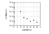
- FIG. 6 is a schematic plan view showing an example of a pixel configuration of an image pickup apparatus having the image pickup device shown in FIG. 24. It is a characteristic figure which showed the relationship between the content of Ga and the carrier mobility in Experimental Example 1 to Experimental Example 6. 6 is a characteristic diagram showing the relationship between the Ga content and the carrier concentration in Experimental Examples 1 to 6. It is sectional drawing which shows an example of the structure of the image sensor which concerns on the modification 4 of this disclosure. It is sectional drawing which shows an example of the structure of the image pickup device which concerns on the modification 5 of this disclosure.
- FIG. 3 is a schematic plan view showing an example of the pixel configuration of the image pickup apparatus having the image pickup device shown in FIG. 30A. It is sectional drawing which shows an example of the structure of the image pickup device which concerns on the modification 7 of this disclosure.
- FIG. 3 is a schematic plan view showing an example of the pixel configuration of the image pickup apparatus having the image pickup device shown in FIG. 31A. It is sectional drawing which shows an example of the structure of the image sensor which concerns on the modification 8 of this disclosure.
- FIG. 3 is a schematic plan view showing an example of the pixel configuration of the image pickup apparatus having the image pickup device shown in FIG. 30A. It is sectional drawing which shows an example of the structure of the image pickup device which concerns on the modification 7 of this disclosure.
- FIG. 3 is a schematic plan view showing an example of the pixel configuration of the image pickup apparatus having the image pickup device
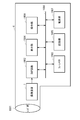
- FIG. 3 is a functional block diagram showing an example of an electronic device (camera) using the imaging device shown in FIG. 33. It is a block diagram which shows another example of the structure of the image pickup apparatus which used the image pickup element shown in FIG. 1 and the like as a pixel.
- FIG. 3 is a block diagram showing another example of the configuration of an electronic device having an imaging device shown in FIG. 33 and the like. It is a block diagram which shows an example of the schematic structure of the body information acquisition system. It is a figure which shows an example of the schematic structure of the endoscopic surgery system. It is a block diagram which shows an example of the functional structure of a camera head and a CCU. It is a block diagram which shows an example of the schematic structure of a vehicle control system. It is explanatory drawing which shows an example of the installation position of the vehicle exterior information detection unit and the image pickup unit.
- Modification 1 (Example in which a protective layer is further provided between the semiconductor layer and the photoelectric conversion layer) 2-2.
- Modification 2 (Example in which a semiconductor layer having a three-layer structure is provided between the lower electrode and the photoelectric conversion layer) 2-3.
- Modification 3 (Example in which a transfer electrode is further provided as a lower electrode) 3.
- Second Embodiment (example of an imaging device having a between the lower electrode and the photoelectric conversion layer, a semiconductor layer composed of two layers having the values of and E VO of a predetermined DerutaEN) 4.
- Modification example 4-1 (Example in which two organic photoelectric conversion parts are laminated on a semiconductor substrate) 4-2.
- Modification 5 (Example in which three organic photoelectric conversion parts are laminated on a semiconductor substrate) 4-3.
- Modification 6 an example of an image sensor that disperses using a color filter) 4-4.
- Modification 7 another example of an image sensor that disperses using a color filter) 4-5.
- Modification 8 Example in which two organic photoelectric conversion parts are laminated on a semiconductor substrate) 5.
- Application example 6. Application example
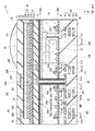
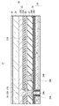
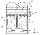
- FIG. 1 shows a cross-sectional configuration of an image pickup device (image pickup device 10) according to the first embodiment of the present disclosure.
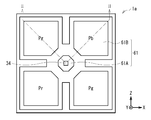
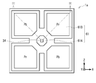
- FIG. 2 schematically shows an example of the planar configuration of the image pickup device 10 shown in FIG. 1
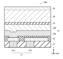
- FIG. 1 shows a cross section taken along the line II shown in FIG.
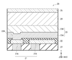
- FIG. 3 is an enlarged schematic representation of an example of the cross-sectional configuration of the main part (organic photoelectric conversion unit 20) of the image sensor 10 shown in FIG.
- the image sensor 10 is arranged in the pixel portion 1A of an image pickup device (for example, image pickup device 1, see FIG.
- CMOS Complementary Metal Oxide Semiconductor
- CMOS Complementary Metal Oxide Semiconductor
- a pixel unit 1a composed of four unit pixels P arranged in 2 rows ⁇ 2 columns is a repeating unit, and is repeated in an array consisting of a row direction and a column direction. Have been placed.
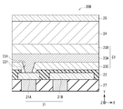
- the image sensor 10 of the present embodiment has a laminated structure between the lower electrode 21 composed of the readout electrode 21A and the storage electrode 21B and the photoelectric conversion layer 24 in the organic photoelectric conversion unit 20 provided on the semiconductor substrate 30.
- the semiconductor layer 23 to be provided is provided.
- the semiconductor layer 23 is composed of, for example, a first semiconductor layer 23A and a second semiconductor layer 23B, and is laminated in this order from the lower electrode 21 side.
- the first semiconductor layer 23A has a value of greater C5s than the value of C5s the second semiconductor layer 23B, the second semiconductor layer 23B, rather than the value of E VO or E VN of the first semiconductor layer 23A It has a large EVO or EVN value.
- the read-out electrode 21A corresponds to a specific example of the "second electrode” of the present disclosure
- the storage electrode 21B corresponds to a specific example of the "first electrode” of the present disclosure
- the first semiconductor layer 23A corresponds to a specific example of the "first layer” of the present disclosure
- the second semiconductor layer 23B corresponds to a specific example of the "second layer” of the present disclosure.
- the image pickup element 10 is, for example, a so-called vertical spectroscopic type in which one organic photoelectric conversion unit 20 and two inorganic photoelectric conversion units 32B and 32R are vertically laminated.
- the organic photoelectric conversion unit 20 is provided on the first surface (back surface) 30A side of the semiconductor substrate 30.
- the inorganic photoelectric conversion units 32B and 32R are embedded and formed in the semiconductor substrate 30, and are laminated in the thickness direction of the semiconductor substrate 30.
- the organic photoelectric conversion unit 20 and the inorganic photoelectric conversion units 32B and 32R selectively detect light in different wavelength ranges and perform photoelectric conversion.
- the organic photoelectric conversion unit 20 acquires a green (G) color signal.
- the inorganic photoelectric conversion units 32B and 32R acquire blue (B) and red (R) color signals, respectively, depending on the difference in absorption coefficient.
- the image sensor 10 can acquire a plurality of types of color signals in one unit pixel P without using a color filter.
- the second surface 30B of the semiconductor substrate 30 for example, floating diffusion (floating diffusion layer) FD1 (region 36B in the semiconductor substrate 30), FD2 (region 37C in the semiconductor substrate 30), FD3 (semiconductor substrate 30) Area 38C), transfer transistors Tr2 and Tr3, amplifier transistor (modulator) AMP, reset transistor RST, and selection transistor SEL are provided.
- the second surface 30B of the semiconductor substrate 30 is further provided with a multilayer wiring layer 40 via a gate insulating layer 33.
- the multilayer wiring layer 40 has, for example, a configuration in which the wiring layers 41, 42, and 43 are laminated in the insulating layer 44.
- a peripheral circuit unit 130 (see FIG. 33) including a logic circuit or the like is provided around the peripheral portion of the semiconductor substrate 30, that is, around the pixel portion 1A.
- the first surface 30A side of the semiconductor substrate 30 is represented as the light incident side S1
- the second surface 30B side is represented as the wiring layer side S2.
- the semiconductor layer 23 and the photoelectric conversion layer 24 formed by using an organic material are laminated in this order from the lower electrode 21 side between the lower electrode 21 and the upper electrode 25 arranged so as to face each other. ing.
- the semiconductor layer 23 as described above, the first semiconductor layer 23A and the second semiconductor layer 23B are laminated in this order from the lower electrode 21 side, and the first semiconductor layer 23A is the value of C5s of the second semiconductor layer 23B. has a value of greater C5s than, the second semiconductor layer 23B has a large value of E VO or E VN than the value of E VO or E VN of the first semiconductor layer 23A.
- the photoelectric conversion layer 24 is composed of a p-type semiconductor and an n-type semiconductor, and has a bulk heterojunction structure in the layer.
- the bulk heterojunction structure is a p / n junction surface formed by mixing p-type semiconductors and n-type semiconductors.
- the organic photoelectric conversion unit 20 further has an insulating layer 22 between the lower electrode 21 and the semiconductor layer 23.
- the insulating layer 22 is provided over the entire surface of the pixel portion 1A, and has an opening 22H on the readout electrode 21A constituting the lower electrode 21, for example.
- the readout electrode 21A is electrically connected to the first semiconductor layer 23A of the semiconductor layer 23 via the opening 22H.
- FIG. 1 shows an example in which the semiconductor layer 23, the photoelectric conversion layer 24, and the upper electrode 25 are separately formed for each image sensor 10, the semiconductor layer 23, the photoelectric conversion layer 24, and the upper electrode 25 are shown.
- it may be provided as a continuous layer common to a plurality of image pickup devices 10.
- an insulating layer 26 and an interlayer insulating layer 27 are provided between the first surface 30A of the semiconductor substrate 30 and the lower electrode 21.
- the insulating layer 26 is composed of a layer having a fixed charge (fixed charge layer) 26A and a dielectric layer 26B having an insulating property.
- the inorganic photoelectric conversion units 32B and 32R have made it possible to disperse light in the vertical direction by utilizing the fact that the wavelength of light absorbed in the semiconductor substrate 30 made of a silicon substrate differs depending on the incident depth of light. Each has a pn junction in a predetermined region of the semiconductor substrate 30.
- a through electrode 34 is provided between the first surface 30A and the second surface 30B of the semiconductor substrate 30.
- the through electrode 34 is electrically connected to the read electrode 21A, and the organic photoelectric conversion unit 20 passes through the through electrode 34 to the gate Gamp of the amplifier transistor AMP and the reset transistor RST (reset transistor) which also serves as the floating diffusion FD1. It is connected to one source / drain region 36B (Tr1rst).
- the electric charge (electrons in this case) generated in the organic photoelectric conversion unit 20 on the first surface 30A side of the semiconductor substrate 30 is transferred to the second surface 30B side of the semiconductor substrate 30 via the through electrode 34. It is possible to transfer the charge well and improve the characteristics.
- the lower end of the through electrode 34 is connected to the connection portion 41A in the wiring layer 41, and the connection portion 41A and the gate Gamp of the amplifier transistor AMP are connected via the lower first contact 45.
- the connecting portion 41A and the floating diffusion FD1 (region 36B) are connected via, for example, a lower second contact 46.
- the upper end of the through electrode 34 is connected to the read electrode 21A via, for example, the pad portion 39A and the upper first contact 39C.
- a protective layer 51 is provided above the organic photoelectric conversion unit 20.
- a wiring 52 and a light-shielding film 53 for electrically connecting the upper electrode 25 and the peripheral circuit portion 130 are provided around the pixel portion 1A.
- an optical member such as a flattening layer (not shown) and an on-chip lens 54 is further arranged.
- the light incident on the organic photoelectric conversion unit 20 from the light incident side S1 is absorbed by the photoelectric conversion layer 24.
- the excitons generated thereby move to the interface between the electron donor and the electron acceptor constituting the photoelectric conversion layer 24, and exciton separation, that is, dissociation into electrons and holes.
- the charges (electrons and holes) generated here differ depending on the diffusion due to the difference in carrier concentration and the internal electric field due to the difference in the work function between the anode (for example, the upper electrode 25) and the cathode (for example, the lower electrode 21). It is carried to the electrode and detected as a photocurrent.
- the transport direction of electrons and holes can also be controlled by applying an electric potential between the lower electrode 21 and the upper electrode 25.
- the organic photoelectric conversion unit 20 is an organic photoelectric conversion element that absorbs green light corresponding to a part or all of a selective wavelength range (for example, 450 nm or more and 650 nm or less) to generate excitons.
- a selective wavelength range for example, 450 nm or more and 650 nm or less
- the lower electrode 21 is composed of, for example, a readout electrode 21A and a storage electrode 21B arranged in parallel on the interlayer insulating layer 27.
- the readout electrode 21A is for transferring the electric charge generated in the photoelectric conversion layer 24 to the floating diffusion FD1, and is, for example, 1 for each pixel unit 1a composed of 4 unit pixels P arranged in 2 rows ⁇ 2 columns. It is provided one by one.
- the read electrode 21A is connected to the floating diffusion FD1 via, for example, the upper first contact 39C, the pad portion 39A, the through electrode 34, the connecting portion 41A, and the lower second contact 46.
- the storage electrode 21B is for storing, for example, electrons in the semiconductor layer 23 as a signal charge among the charges generated in the photoelectric conversion layer 24, and is provided for each unit pixel P.
- the storage electrode 21B is provided for each unit pixel P in a region that faces the light receiving surfaces of the inorganic photoelectric conversion units 32B and 32R formed in the semiconductor substrate 30 and covers these light receiving surfaces.
- the storage electrode 21B is preferably larger than the readout electrode 21A, which allows a large amount of charge to be stored.
- the lower electrode 21 is made of a light-transmitting conductive film, for example, ITO (indium tin oxide).
- ITO indium tin oxide
- a tin oxide (SnO 2 ) -based material to which a dopant is added or a zinc oxide-based material obtained by adding a dopant to zinc oxide (ZnO) may be used.
- the zinc oxide-based material include aluminum zinc oxide (AZO) to which aluminum (Al) is added as a dopant, gallium zinc oxide (GZO) to which gallium (Ga) is added, and indium zinc to which indium (In) is added.
- Oxide (IZO) can be mentioned.
- IGZO, ITZO, CuI, InSbO 4, ZnMgO, CuInO 2, MgIN 2 O 4 may be used CdO or ZnSnO 3, and the like.
- the insulating layer 22 is for electrically separating the storage electrode 21B and the semiconductor layer 23.
- the insulating layer 22 is provided on, for example, the interlayer insulating layer 27 so as to cover the lower electrode 21.
- the insulating layer 22 is provided with an opening 22H above the read-out electrode 21A of the lower electrodes 21, and the read-out electrode 21A and the semiconductor layer 23 are electrically connected via the opening 22H.
- the insulating layer 22 is composed of, for example, a single-layer film made of one of silicon oxide (SiO x ), silicon nitride (SiN x ), silicon oxynitride (SiON), and a laminated film made of two or more. There is.
- the thickness of the insulating layer 22 is, for example, 20 nm or more and 500 nm or less.
- the semiconductor layer 23 is for accumulating the electric charge generated in the photoelectric conversion layer 24.
- the semiconductor layer 23 is provided between the lower electrode 21 and the photoelectric conversion layer 24, and the first semiconductor layer 23A and the second semiconductor layer 23B are laminated in this order from the lower electrode 21 side. It has a laminated structure.
- the first semiconductor layer 23A is provided on the insulating layer 22 that electrically separates the lower electrode 21 and the semiconductor layer 23, and the read electrode 21A is provided in the opening 22H provided on the read electrode 21A. Is directly electrically connected to.
- the second semiconductor layer 23B is provided between the first semiconductor layer 23A and the photoelectric conversion layer 24.
- the semiconductor layer 23 can be formed by using, for example, an oxide semiconductor material.
- an oxide semiconductor material since electrons are used as signal charges among the charges generated in the photoelectric conversion layer 24, the semiconductor layer 23 can be formed by using an n-type oxide semiconductor material.
- the first semiconductor layer 23A is for preventing the electric charge accumulated in the semiconductor layer 23 from being trapped at the interface with the insulating layer 22 and efficiently transferring the electric charge to the read electrode 21A.
- the second semiconductor layer 23B is for preventing the desorption of oxygen on the surface of the first semiconductor layer 23A and preventing the electric charge generated in the photoelectric conversion layer 24 from being trapped at the interface with the photoelectric conversion layer 24. .. Therefore, the first semiconductor layer 23A can be formed by including an oxide semiconductor material having a value of C5s larger than the value of C5s of the second semiconductor layer 23B.
- the second semiconductor layer 23B can be formed by including an oxide semiconductor material having an EVO value larger than the EVO value of the first semiconductor layer 23A.
- the first semiconductor layer 23A can be formed by including an oxide semiconductor material satisfying C5s> 50%, more preferably an oxide semiconductor material satisfying C5s> 80%.
- the second semiconductor layer 23B is an oxide semiconductor material that satisfies E VO> 2.3 eV, more preferably, may be formed to include an oxide semiconductor material that satisfies E VO> 2.8 eV.
- C5s is a value indicating the contribution ratio of the 5s orbital to the bottom of the conduction band (Conduction Band Minimum: CBM).
- CBM Conduction Band Minimum
- the CMB of an oxide semiconductor is made by mixing the s orbitals of each metal element. Among them, when the ratio of the 5s orbitals (s orbitals of cadmium (Cd), indium (In) and tin (Sn)) having the largest spatial spread is large, the number of transfer traps decreases.
- C5s can be obtained from, for example, first-principles calculation.
- a model is created by the calculation method used when calculating the oxygen defect generation energy described later.
- the number of oxygen atoms is modeled by the number calculated from the valence without decreasing, as in the method of calculating the oxygen defect generation energy.
- From the electronic state obtained when calculating the model the orbital corresponding to CBM is specified.
- the CBM is the smallest energy orbit in which an electron is unoccupied.
- the contribution ratio of the 5s orbitals (s orbitals of Cd, In and Sn) to the CBM is determined.
- VASP Vienna Ab Initio Simulation Package
- PROCAR Partial Density Of States
- EVO refers to the average value of oxygen deficiency generation energy possessed by a plurality of types of metal atoms. It can be said that the higher the value of the oxygen deficiency generation energy, the more difficult it is for oxygen atoms to be desorbed, and the more difficult it is for oxygen atoms, oxygen molecules, or other atoms or molecules to be taken in, so that it is stable.
- the oxygen deficiency generation energy EVO can be obtained from, for example, first-principles calculation, and is calculated from the following mathematical formula (1). Specifically, first, an amorphous structure having the same ratio of atoms as the target metal element composition and the corresponding oxygen number is created. As the oxygen number, a general metal ion valence is used. That is, zinc (Zn) and Cd are +2 valence, gallium (Ga) and In are +3 valence, and germanium (Ge) and Sn are +4 valence. Oxygen ion is -2 valent and contains a few neutral oxygen. Further, it is desirable that the total number of atoms is 80 or more.
- the first semiconductor layer 23A can be formed as, for example, an amorphous layer. As a result, it is possible to prevent an increase in the carrier density of the first semiconductor layer 23A and realize a low carrier concentration. Further, as compared with the case where the first semiconductor layer 23A is formed as a crystal layer, the generation of dangling bonds at the grain boundaries in the first semiconductor layer 23A and the interface with the insulating layer 22 is suppressed, and the trap is lower. Can be transformed into.
- the film quality of the second semiconductor layer 23B is not particularly limited, and may be a crystal layer or may be formed as an amorphous layer.
- the amorphous layer and the crystal layer can be judged by the presence or absence of haloing of the fast Fourier transform (FFT) image of the transmission electron microscope (TEM) image.
- FFT fast Fourier transform
- TEM transmission electron microscope
- a bright and dark striped image corresponding to both intervals of the lattice appears on the crystal layer due to the interference between the diffracted wave and the transmitted wave from the lattice surface having the crystal. This is called a plaid.
- no plaid is confirmed.
- FFTing the TEM image in two dimensions the patterns shown in FIGS. 4 and 5 can be confirmed.
- the crystal layer as shown in FIG.
- a speckled pattern extending in one direction corresponding to the period of the plaid can be confirmed.
- a broad ring-shaped pattern can be confirmed. This is halo ring.
- FIGS. 4 and 5 show the correspondence between the patterns of the crystal layer and the amorphous layer shown in FIGS. 4 and 5, respectively, and their strength profiles.
- the unit pixel P is 30 pixels in the horizontal direction of the paper surface for the FFT pattern of the rectangular square region of the thickness ⁇ width 45 nm of each of the crystal layer and the amorphous layer (FIGS. 4 and 5).
- Area X) is the actual intensity profile (histogram) integrated.
- the intensity profile of the crystal layer three peaks corresponding to the three filled spots can be confirmed in FIG. 4, whereas the intensity profile of the amorphous layer is broad.
- Examples of the constituent materials of the semiconductor layer 23 include ITO, IZO, IGO, ZTO, IGZO (In—Ga—Zn—O-based oxide semiconductor), and GZTO (Ga).
- -Zn-Sn-O-based oxide semiconductors ITZO (In-Sn-Zn-O-based oxide semiconductors), IGZTO (In-Ga-Zn-Sn-O-based oxide semiconductors), and the like.
- IGTO In—Ga—Sn—O-based oxide semiconductor
- the semiconductor layer 23 may contain, for example, silicon (Si), aluminum (Al), titanium (Ti), molybdenum (Mo), carbon (C), cadmium (Cd) and the like.
- the first semiconductor layer 23A is preferably formed by using ITO, IZO, indium-rich ITZO (cation ratio In> 50%), IGO or tin-rich SnZNO (cation ratio Sn> 50%). More specifically, the first semiconductor layer 23A can be formed by using , for example, In 2 O 3 (ITO) to which 10 wt% of SnO 2 is added or In 2 O 3 (IZO) to which 10 wt% of ZnO is added. preferable. As the second semiconductor layer 23B, it is preferable to use IGZO, IGZTO, ZTO, GZTO or IGTO.
- ZTO having a cation ratio of Zn> 60%
- In + Sn having a cation ratio of 50% or less and a ratio of Ga + An.
- Is preferably formed using IGZTO of 50% or more.
- C5s in the above material can be adjusted as follows. First, a candidate composition (cation ratio) is determined, and a sufficient number of oxygens that become neutral when the cation is ionized are added. At this time, the number of cations is preferably about 30 to 40 or more.
- the valence of Sn is +4, the valence of In is +3, the valence of Ga is +3, the valence of Zn is +2, and the valence of O is -2.
- the value of C5s of the target composition can be calculated.
- the value of C5s tends to increase as the number of 5s elements such as In and Sn increases.
- C5s> satisfy 80%, such as ITO the first semiconductor layer 23A using a (In 2 O 3 having a SnO 2 was added 10 wt%), satisfies the E VO> 2.8V, for example, IGZO (an In: It represents the elemental composition in the semiconductor layer 23 when the second semiconductor layer 23B is formed using Ga: Zn 1: 1: 1).
- the charges accumulated in the semiconductor layer 23 from the photoelectric conversion layer 24 are as shown in FIG. In addition, it is trapped in the 4s orbit of Ga, and its movement to the read electrode 21A is hindered.
- the thickness of the first semiconductor layer 23A is, for example, 2 nm or more and 10 nm or less.
- the thickness of the second semiconductor layer 23B is, for example, 15 nm or more and 100 nm or less.
- the ratio (t2 / t1) of the thickness (t2) of the second semiconductor layer 23B to the thickness (t1) of the first semiconductor layer 23A is preferably 4 or more and 8 or less.
- Table 1 shows the films of the first semiconductor layer 23A and the second semiconductor layer 23B calculated from the ID- V GS curves obtained by manufacturing a simple TFT (Thin-Film-Transistor) element and evaluating the TFT. This is a summary of the on-voltages of the thickness ratio (t2 / t1).
- the TFT element is formed by forming a SiO 2 film, a first semiconductor layer 23A, and a second semiconductor layer 23B in this order on a silicon substrate, and providing a source electrode and a drain electrode on the second semiconductor layer 23B.
- the first semiconductor layer 23A is an amorphous layer as described above, it is possible to realize a low carrier concentration while preventing an increase in the carrier density of the semiconductor layer 23.
- the constituent materials of the first semiconductor layer 23A and the second semiconductor layer 23B a nitride semiconductor material or an oxynitride semiconductor material can be used in addition to the oxide semiconductor material.
- the nitrogen deficiency generation energy EVN is used as an index instead of the oxygen deficiency generation energy EVO. That is, the second semiconductor layer 23B may be formed to include a nitride semiconductor material having a large value of E VN than the value of E VN of the first semiconductor layer 23A (eg, E VN> 2.3 eV) .
- the nitrogen deficiency generation energy EVN can be similarly calculated by replacing the oxygen atom with the nitrogen atom in the above-mentioned calculation method of the oxygen deficiency generation energy EVO.
- the photoelectric conversion layer 24 is for converting light energy into electrical energy.
- the photoelectric conversion layer 24 is composed of, for example, two or more types of organic materials (p-type semiconductor materials or n-type semiconductor materials) that function as p-type semiconductors or n-type semiconductors, respectively.
- the photoelectric conversion layer 24 has a bonding surface (p / n bonding surface) between the p-type semiconductor material and the n-type semiconductor material in the layer.
- the p-type semiconductor functions relatively as an electron donor (donor), and the n-type semiconductor functions relatively as an electron acceptor (acceptor).
- the photoelectric conversion layer 24 provides a place where excitons generated when light is absorbed are separated into electrons and holes. Specifically, the interface between the electron donor and the electron acceptor (p /). At the n junction surface), excitons separate into electrons and holes.
- the photoelectric conversion layer 24 includes, in addition to the p-type semiconductor material and the n-type semiconductor material, an organic material that photoelectrically converts light in a predetermined wavelength range while transmitting light in another wavelength range, that is, a so-called dye material. It may have been done.
- the photoelectric conversion layer 24 is formed using three types of organic materials, a p-type semiconductor material, an n-type semiconductor material, and a dye material, the p-type semiconductor material and the n-type semiconductor material are in the visible region (for example, from 450 nm). It is preferable that the material has light transmission at 800 nm).
- the thickness of the photoelectric conversion layer 24 is, for example, 50 nm or more and 500 nm or less.
- the photoelectric conversion layer 24 of the present embodiment contains an organic material and has absorption between visible light and near infrared light.
- the organic material constituting the photoelectric conversion layer 24 include quinacridone derivatives, naphthalene derivatives, anthracene derivatives, phenanthrene derivatives, tetracene derivatives, pyrene derivatives, perylene derivatives and fluoranthene derivatives.
- the photoelectric conversion layer 24 is composed of a combination of two or more of the above organic materials.
- the organic material functions as a p-type semiconductor or an n-type semiconductor depending on the combination thereof.
- the organic material constituting the photoelectric conversion layer 24 is not particularly limited.
- polymers such as phenylene vinylene, fluorene, carbazole, indole, pyrrole, pyrrole, picolin, thiophene, acetylene and diacetylene or derivatives thereof can be used.
- metal complex dyes cyanine dyes, merocyanine dyes, phenylxanthene dyes, triphenylmethane dyes, rodacyanine dyes, xanthene dyes, macrocyclic azaanulene dyes, azulene dyes, naphthoquinone dyes, anthraquinone dyes.
- Pyrene and other condensed polycyclic aromatic compounds chain compounds fused with aromatic rings or heterocyclic compounds, and two nitrogen-containing heterocycles such as quinoline, benzothiazole, and benzoxanthene having a squarylium group and a croconitecmethine group as bonding chains.
- a cyanine-based dye or the like bonded by a squarylium group and a croconitecmethine group can be used.
- the metal complex dye include a dithiol metal complex dye, a metal phthalocyanine dye, a metal porphyrin dye, and a ruthenium complex dye. Of these, ruthenium complex dyes are particularly preferable, but are not limited to the above.
- the upper electrode 25 is made of a conductive film having light transmission like the lower electrode 21, and is made of, for example, ITO.
- ITO a tin oxide (SnO 2 ) -based material to which a dopant is added or a zinc oxide-based material obtained by adding a dopant to zinc oxide (ZnO) is used. May be good.
- the zinc oxide-based material include aluminum zinc oxide (AZO) to which aluminum (Al) is added as a dopant, gallium zinc oxide (GZO) to which gallium (Ga) is added, and indium zinc to which indium (In) is added.
- Oxide (IZO) can be mentioned.
- the upper electrode 25 may be separated for each unit pixel P, or may be formed as an electrode common to each unit pixel P.
- the thickness of the upper electrode 25 is, for example, 10 nm or more and 200 nm or less.
- the photoelectric conversion layer 24 and the lower electrode 21 are provided between the photoelectric conversion layer 24 and the lower electrode 21 (for example, between the semiconductor layer 23 and the photoelectric conversion layer 24) and between the photoelectric conversion layer 24 and the upper electrode 25.
- the semiconductor layer 23, the buffer layer also serving as an electron blocking film, the photoelectric conversion layer 24, the buffer layer also serving as a hole blocking film, the work function adjusting layer, and the like may be laminated in this order from the lower electrode 21 side.
- the photoelectric conversion layer 24 may have, for example, a pin bulk heterostructure in which a p-type blocking layer, a layer (i layer) containing a p-type semiconductor and an n-type semiconductor, and an n-type blocking layer are laminated.
- the insulating layer 26 covers the first surface 30A of the semiconductor substrate 30, reduces the interface state with the semiconductor substrate 30, and suppresses the generation of dark current from the interface with the semiconductor substrate 30. Further, the insulating layer 26 extends from the first surface 30A of the semiconductor substrate 30 to the side surface of the opening 34H (see FIG. 14) in which the through electrodes 34 penetrating the second surface 30B are formed.
- the insulating layer 26 has, for example, a laminated structure of a fixed charge layer 26A and a dielectric layer 26B.
- the fixed charge layer 26A may be a film having a positive fixed charge or a film having a negative fixed charge.
- the constituent material of the fixed charge layer 26A it is preferable to use a semiconductor material or a conductive material having a bandgap wider than that of the semiconductor substrate 30. As a result, it is possible to suppress the generation of dark current at the interface of the semiconductor substrate 30.
- the constituent materials of the fixed charge layer 26A include hafnium oxide (HfO x ), aluminum oxide (AlO x ), zirconium oxide (ZrO x ), tantalum oxide (TaO x ), titanium oxide (TIO x ), and lanthanum oxide (Tio x).
- the dielectric layer 26B is for preventing the reflection of light caused by the difference in refractive index between the semiconductor substrate 30 and the interlayer insulating layer 27.
- the constituent material of the dielectric layer 26B is preferably a material having a refractive index between the refractive index of the semiconductor substrate 30 and the refractive index of the interlayer insulating layer 27.
- Examples of the constituent material of the dielectric layer 26B include silicon oxide, TEOS, silicon nitride, silicon oxynitride (SiON) and the like.
- the interlayer insulating layer 27 is composed of, for example, a single-layer film made of one of silicon oxide, silicon nitride, silicon oxynitride, and the like, or a laminated film made of two or more of these.
- a shield electrode 28 is provided on the interlayer insulating layer 27 together with a lower electrode 21.
- the shield electrode 28 is for preventing capacitive coupling between adjacent pixel units 1a.
- the shield electrode 28 is provided and fixed around a pixel unit 1a composed of four unit pixels P arranged in 2 rows ⁇ 2 columns. An electric potential is applied.
- the shield electrode 28 further extends in the pixel unit 1a between unit pixels P adjacent to each other in the row direction (Z-axis direction) and the column direction (X-axis direction).
- the semiconductor substrate 30 is composed of, for example, an n-type silicon (Si) substrate, and has a p-well 31 in a predetermined region.
- the inorganic photoelectric conversion units 32B and 32R are each composed of a photodiode (PD) having a pn junction in a predetermined region of the semiconductor substrate 30, and the wavelength of light absorbed by the Si substrate according to the incident depth of light is set. It is possible to disperse light in the vertical direction by utilizing different things.
- the inorganic photoelectric conversion unit 32B selectively detects blue light and accumulates a signal charge corresponding to blue light, and is installed at a depth at which blue light can be efficiently photoelectrically converted.
- the inorganic photoelectric conversion unit 32R selectively detects red light and accumulates a signal charge corresponding to red, and is installed at a depth at which red light can be efficiently photoelectrically converted.
- Blue (B) is, for example, a color corresponding to a wavelength range of 450 nm or more and 495 nm or less
- red (R) is a color corresponding to, for example, a wavelength range of 620 nm or more and 750 nm or less. It suffices that the inorganic photoelectric conversion units 32B and 32R can detect light in a part or all of each wavelength range, respectively.
- the inorganic photoelectric conversion unit 32B includes, for example, a p + region serving as a hole storage layer and an n region serving as an electron storage layer.
- the inorganic photoelectric conversion unit 32R has, for example, a p + region serving as a hole storage layer and an n region serving as an electron storage layer (having a pn-p laminated structure).
- the n region of the inorganic photoelectric conversion unit 32B is connected to the vertical transfer transistor Tr2.
- the p + region of the inorganic photoelectric conversion unit 32B is bent along the transfer transistor Tr2 and is connected to the p + region of the inorganic photoelectric conversion unit 32R.
- the gate insulating layer 33 is composed of, for example, a single-layer film made of one of silicon oxide, silicon nitride, silicon oxynitride, and the like, or a laminated film made of two or more of these.
- the through electrode 34 is provided between the first surface 30A and the second surface 30B of the semiconductor substrate 30, and has a function as a connector between the organic photoelectric conversion unit 20 and the gate Gamp and the floating diffusion FD1 of the amplifier transistor AMP. , It serves as a transmission path for the electric charge generated in the organic photoelectric conversion unit 20.
- the reset gate Grst of the reset transistor RST is arranged next to the floating diffusion FD1 (one source / drain region 36B of the reset transistor RST). As a result, the electric charge accumulated in the floating diffusion FD1 can be reset by the reset transistor RST.
- the pad portions 39A and 39B, the upper first contact 39C, the upper second contact 39D, the lower first contact 45, the lower second contact 46 and the wiring 52 are made of a doped silicon material such as PDAS (Phosphorus Doped Amorphous Silicon).
- PDAS Phosphorus Doped Amorphous Silicon
- it can be formed using a metal material such as aluminum (Al), tungsten (W), titanium (Ti), cobalt (Co), hafnium (Hf) and tantalum (Ta).
- the protective layer 51 and the on-chip lens 54 are made of a light-transmitting material, for example, a single-layer film made of silicon oxide, silicon nitride, silicon oxynitride, or the like, or two of them. It is composed of the above-mentioned laminated film.
- the thickness of the protective layer 51 is, for example, 100 nm or more and 30,000 nm or less.
- the light-shielding film 53 is provided in the protective layer 51 together with the wiring 52 so as to cover the region of the readout electrode 21A which is in direct contact with the semiconductor layer 23 without covering at least the storage electrode 21B.
- the light-shielding film 53 can be formed by using, for example, tungsten (W), aluminum (Al), an alloy of Al and copper (Cu), or the like.
- FIG. 11 is an equivalent circuit diagram of the image pickup device 10 shown in FIG.
- FIG. 12 schematically shows the arrangement of the lower electrode 21 of the image pickup device 10 shown in FIG. 1 and the transistors constituting the control unit.
- the reset transistor RST (reset transistor TR1rst) is for resetting the electric charge transferred from the organic photoelectric conversion unit 20 to the floating diffusion FD1, and is composed of, for example, a MOS transistor.
- the reset transistor TR1rst is composed of a reset gate Grst, a channel forming region 36A, and source / drain regions 36B and 36C.
- the reset gate Grst is connected to the reset line RST1, and one source / drain region 36B of the reset transistor TR1rst also serves as a floating diffusion FD1.
- the other source / drain region 36C constituting the reset transistor TR1rst is connected to the power supply line VDD.
- the amplifier transistor AMP is a modulation element that modulates the amount of electric charge generated by the organic photoelectric conversion unit 20 into a voltage, and is composed of, for example, a MOS transistor. Specifically, the amplifier transistor AMP is composed of a gate Gamp, a channel forming region 35A, and source / drain regions 35B and 35C.
- the gate Gamp is connected to one source / drain region 36B (floating diffusion FD1) of the read electrode 21A and the reset transistor TR1rst via the lower first contact 45, the connecting portion 41A, the lower second contact 46, the through electrode 34, and the like. Has been done. Further, one source / drain region 35B shares an region with the other source / drain region 36C constituting the reset transistor TR1rst, and is connected to the power supply line VDD.
- the selection transistor SEL selection transistor TR1sel
- the selection transistor SEL is composed of a gate Gsel, a channel formation region 34A, and source / drain regions 34B and 34C.
- the gate Gsel is connected to the selection line SEL1.
- One source / drain region 34B shares an area with the other source / drain region 35C constituting the amplifier transistor AMP, and the other source / drain region 34C is connected to the signal line (data output line) VSL1. Has been done.
- the transfer transistor TR2 (transfer transistor TR2trs) is for transferring the signal charge corresponding to the blue color generated and accumulated in the inorganic photoelectric conversion unit 32B to the floating diffusion FD2. Since the inorganic photoelectric conversion unit 32B is formed at a position deep from the second surface 30B of the semiconductor substrate 30, it is preferable that the transfer transistor TR2trs of the inorganic photoelectric conversion unit 32B is composed of a vertical transistor.
- the transfer transistor TR2trs is connected to the transfer gate line TG2.
- a floating diffusion FD2 is provided in a region 37C near the gate Gtrs2 of the transfer transistor TR2trs. The charge accumulated in the inorganic photoelectric conversion unit 32B is read out to the floating diffusion FD2 via a transfer channel formed along the gate Gtrs2.
- the transfer transistor TR3 (transfer transistor TR3trs) is for transferring the signal charge corresponding to the accumulated red color generated in the inorganic photoelectric conversion unit 32R to the floating diffusion FD3, and is composed of, for example, a MOS transistor. ..
- the transfer transistor TR3trs is connected to the transfer gate line TG3.
- a floating diffusion FD3 is provided in the region 38C near the gate Gtrs3 of the transfer transistor TR3trs.
- the charge accumulated in the inorganic photoelectric conversion unit 32R is read out to the floating diffusion FD3 via a transfer channel formed along the gate Gtrs3.
- a reset transistor TR2rst On the second surface 30B side of the semiconductor substrate 30, a reset transistor TR2rst, an amplifier transistor TR2amp, and a selection transistor TR2sel that form a control unit of the inorganic photoelectric conversion unit 32B are further provided. Further, a reset transistor TR3rst, an amplifier transistor TR3amp, and a selection transistor TR3sel, which form a control unit of the inorganic photoelectric conversion unit 32R, are provided.
- the reset transistor TR2rst is composed of a gate, a channel forming region, and a source / drain region.
- the gate of the reset transistor TR2rst is connected to the reset line RST2, and one source / drain region of the reset transistor TR2rst is connected to the power supply line VDD.
- the other source / drain region of the reset transistor TR2rst also serves as a floating diffusion FD2.
- the amplifier transistor TR2amp is composed of a gate, a channel forming region, and a source / drain region.
- the gate is connected to the other source / drain region (floating diffusion FD2) of the reset transistor TR2rst.
- One source / drain region constituting the amplifier transistor TR2amp shares an region with one source / drain region constituting the reset transistor TR2rst, and is connected to the power supply line VDD.
- the selection transistor TR2sel is composed of a gate, a channel forming region, and a source / drain region.
- the gate is connected to the selection line SEL2.
- One source / drain region constituting the selection transistor TR2sel shares an region with the other source / drain region constituting the amplifier transistor TR2amp.
- the other source / drain region constituting the selection transistor TR2sel is connected to the signal line (data output line) VSL2.
- the reset transistor TR3rst is composed of a gate, a channel forming region, and a source / drain region.
- the gate of the reset transistor TR3rst is connected to the reset line RST3, and one source / drain region constituting the reset transistor TR3rst is connected to the power supply line VDD.
- the other source / drain region constituting the reset transistor TR3rst also serves as a floating diffusion FD3.
- the amplifier transistor TR3amp is composed of a gate, a channel forming region, and a source / drain region.
- the gate is connected to the other source / drain region (floating diffusion FD3) constituting the reset transistor TR3rst.
- One source / drain region constituting the amplifier transistor TR3amp shares an region with one source / drain region constituting the reset transistor TR3rst, and is connected to the power supply line VDD.
- the selection transistor TR3sel is composed of a gate, a channel forming region, and a source / drain region.
- the gate is connected to the selection line SEL3.
- One source / drain region constituting the selection transistor TR3sel shares an region with the other source / drain region constituting the amplifier transistor TR3amp.
- the other source / drain region constituting the selection transistor TR3sel is connected to the signal line (data output line) VSL3.
- the reset lines RST1, RST2, RST3, selection lines SEL1, SEL2, SEL3, and transfer gate lines TG2, TG3 are each connected to a vertical drive circuit constituting the drive circuit.
- the signal lines (data output lines) VSL1, VSL2, and VSL3 are connected to the column signal processing circuit 113 constituting the drive circuit.
- the image sensor 10 of the present embodiment can be manufactured, for example, as follows.
- FIG. 13 to 18 show the manufacturing method of the image sensor 10 in the order of processes.
- a p-well 31 is formed in the semiconductor substrate 30, and for example, n-type inorganic photoelectric conversion units 32B and 32R are formed in the p-well 31.
- a p + region is formed in the vicinity of the first surface 30A of the semiconductor substrate 30.
- the second surface 30B of the semiconductor substrate 30 is formed with an n + region to be, for example, floating diffusion FD1 to FD3, and then the gate insulating layer 33, the transfer transistor Tr2, and the transfer transistor Tr3 are selected.
- a gate wiring layer 47 including each gate of the transistor SEL, the amplifier transistor AMP, and the reset transistor RST is formed.
- the transfer transistor Tr2, the transfer transistor Tr3, the selection transistor SEL, the amplifier transistor AMP, and the reset transistor RST are formed.
- a multilayer wiring layer 40 composed of wiring layers 41 to 43 including a lower first contact 45, a lower second contact 46, and a connecting portion 41A and an insulating layer 44 is formed on the second surface 30B of the semiconductor substrate 30.
- an SOI (Silicon on Insulator) substrate in which a semiconductor substrate 30, an embedded oxide film (not shown), and a holding substrate (not shown) are laminated is used.
- the embedded oxide film and the holding substrate are bonded to the first surface 30A of the semiconductor substrate 30. After ion implantation, annealing is performed.
- a support substrate (not shown) or another semiconductor substrate is bonded onto the multilayer wiring layer 40 provided on the second surface 30B side of the semiconductor substrate 30, and the semiconductor substrate 30 is turned upside down. Subsequently, the semiconductor substrate 30 is separated from the embedded oxide film and the holding substrate of the SOI substrate to expose the first surface 30A of the semiconductor substrate 30.
- CMOS processes such as ion implantation and CVD (Chemical Vapor Deposition) methods.
- the semiconductor substrate 30 is processed from the first surface 30A side by, for example, dry etching to form, for example, an annular opening 34H.
- the depth of the opening 34H penetrates from the first surface 30A to the second surface 30B of the semiconductor substrate 30, and reaches, for example, the connection portion 41A.
- a negative fixed charge layer 26A and a dielectric layer 26B are sequentially formed on the first surface 30A and the side surface of the opening 34H of the semiconductor substrate 30.
- the fixed charge layer 26A can be formed, for example, by forming a hafnium oxide film or an aluminum oxide film using an atomic layer deposition method (ALD method).
- the dielectric layer 26B can be formed, for example, by forming a silicon oxide film using a plasma CVD method.
- pad portions 39A and 39B in which a barrier metal made of a laminated film of titanium and titanium nitride (Ti / TiN film) and a tungsten film are laminated are formed at predetermined positions on the dielectric layer 26B. ..
- the pad portions 39A and 39B can be used as a light-shielding film.
- the interlayer insulating layer 27 is formed on the dielectric layer 26B and the pad portions 39A and 39B, and the surface of the interlayer insulating layer 27 is flattened by using a CMP (Chemical Mechanical Polishing) method.
- a conductive material such as Al is embedded in the openings 27H1,27H2, and the upper first contact 39C is formed. And the upper second contact 39D is formed.
- a conductive film 21x is formed on the interlayer insulating layer 27 by, for example, a sputtering method, and then patterning is performed using a photolithography technique. Specifically, after forming a photoresist PR at a predetermined position of the conductive film 21x, the conductive film 21x is processed by dry etching or wet etching. After that, by removing the photoresist PR, the readout electrode 21A and the storage electrode 21B are formed as shown in FIG.
- a semiconductor layer 23 composed of an insulating layer 22, a first semiconductor layer 23A and a second semiconductor layer 23B, a photoelectric conversion layer 24, and an upper electrode 25 are formed.
- the insulating layer 22 for example, a silicon oxide film is formed by using the ALD method, and then the surface of the insulating layer 22 is flattened by using the CMP method. Then, the opening 22H is formed on the readout electrode 21A by, for example, wet etching.
- the semiconductor layer 23 can be formed, for example, by using a sputtering method.
- the photoelectric conversion layer 24 is formed, for example, by using a vacuum vapor deposition method.
- the upper electrode 25 is formed by, for example, a sputtering method. Finally, the protective layer 51, the wiring 52, the light-shielding film 53, and the on-chip lens 54 are arranged on the upper electrode 25. As a result, the image sensor 10 shown in FIG. 1 is completed.
- a buffer layer that also serves as an electron blocking film As described above, between the semiconductor layer 23 and the photoelectric conversion layer 24 and between the photoelectric conversion layer 24 and the upper electrode 25, a buffer layer that also serves as an electron blocking film, a buffer layer that also serves as a hole blocking film, or When forming other layers containing an organic material such as a work function adjusting layer, it is desirable to form each layer continuously (in a vacuum integrated process) in a vacuum process. Further, the film forming method of the photoelectric conversion layer 24 is not necessarily limited to the method using the vacuum vapor deposition method, and for example, a spin coating technique, a printing technique, or the like may be used.
- a vacuum vapor deposition method a reactive vapor deposition method, an electron beam vapor deposition method, an ion plating method, etc.
- CVD method Various chemical vapor deposition methods (CVD method) including physical vapor deposition method (PVD method), pyrosol method, thermal decomposition method for organic metal compounds, spray method, dip method, MOCVD method, electroless plating method And the electrolytic plating method can be mentioned.
- the organic photoelectric conversion unit 20 is connected to the gate Gamp of the amplifier transistor AMP and the floating diffusion FD1 via the through electrode 34. Therefore, the electrons of the excitons generated by the organic photoelectric conversion unit 20 are taken out from the lower electrode 21 side, transferred to the second surface 30S2 side of the semiconductor substrate 30 via the through electrode 34, and accumulated in the floating diffusion FD1. Will be done.
- the amplifier transistor AMP modulates the amount of charge generated in the organic photoelectric conversion unit 20 into a voltage.
- the reset gate Grst of the reset transistor RST is arranged next to the floating diffusion FD1. As a result, the electric charge accumulated in the floating diffusion FD1 is reset by the reset transistor RST.
- the organic photoelectric conversion unit 20 is connected not only to the amplifier transistor AMP but also to the floating diffusion FD1 via the through electrode 34, the electric charge accumulated in the floating diffusion FD1 can be easily reset by the reset transistor RST. It will be possible.
- FIG. 19 shows an operation example of the image sensor 10.
- A shows the potential at the storage electrode 21B
- B shows the potential at the floating diffusion FD1 (reading electrode 21A)
- C shows the potential at the gate (Gsel) of the reset transistor TR1rst. Is.
- a voltage is individually applied to the readout electrode 21A and the storage electrode 21B.
- the potential V1 is applied to the readout electrode 21A from the drive circuit and the potential V2 is applied to the storage electrode 21B during the storage period.
- the potentials V1 and V2 are set to V2> V1.
- the electric charge (signal charge; electron) generated by the photoelectric conversion is attracted to the storage electrode 21B and accumulated in the region of the semiconductor layer 23 facing the storage electrode 21B (storage period).
- the potential in the region of the semiconductor layer 23 facing the storage electrode 21B becomes a more negative value with the passage of time of photoelectric conversion.
- the holes are sent from the upper electrode 25 to the drive circuit.
- the image sensor 10 is reset at a later stage of the storage period. Specifically, at timing t1, the scanning unit changes the voltage of the reset signal RST from a low level to a high level. As a result, in the unit pixel P, the reset transistor TR1rst is turned on, and as a result, the voltage of the floating diffusion FD1 is set to the power supply voltage, and the voltage of the floating diffusion FD1 is reset (reset period).
- the electric charge is read out. Specifically, at the timing t2, the potential V3 is applied to the reading electrode 21A from the drive circuit, and the potential V4 is applied to the storage electrode 21B. Here, the potentials V3 and V4 are set to V3 ⁇ V4. As a result, the electric charge accumulated in the region corresponding to the storage electrode 21B is read out from the read electrode 21A to the floating diffusion FD1. That is, the electric charge accumulated in the semiconductor layer 23 is read out to the control unit (transfer period).
- the potential V1 is applied to the read electrode 21A from the drive circuit again, and the potential V2 is applied to the storage electrode 21B.
- the electric charge generated by the photoelectric conversion is attracted to the storage electrode 21B and accumulated in the region of the photoelectric conversion layer 24 facing the storage electrode 21B (accumulation period).
- the inorganic photoelectric conversion unit 32R electrons corresponding to the incident red light are accumulated in the n region of the inorganic photoelectric conversion unit 32R, and the accumulated electrons are transferred to the floating diffusion FD3 by the transfer transistor Tr3.
- the image sensor 10 of the present embodiment has the first semiconductor layer 23A and the first semiconductor layer 23A from the lower electrode 21 side between the lower electrode 21 composed of the readout electrode 21A and the storage electrode 21B and the photoelectric conversion layer 24.
- the semiconductor layer 23 in which the second semiconductor layer 23B is laminated in this order is provided.
- the first semiconductor layer 23A has a value of greater C5s than the value of C5s the second semiconductor layer 23B, the second semiconductor layer 23B, rather than the value of E VO or E VN of the first semiconductor layer 23A It has a large EVO or EVN value.
- the transport characteristics of the electric charges accumulated in the semiconductor layer 23 above the storage electrode 21B in the in-plane direction are improved. Further, the desorption of oxygen or nitrogen from the first semiconductor layer 23A is reduced, and the occurrence of traps at the interface between the semiconductor layer 23 and the photoelectric conversion layer 24 is reduced. This will be described below.
- a stacked image sensor in which a plurality of photoelectric conversion units are vertically laminated has been developed.
- a laminated image sensor for example, two inorganic photoelectric conversion units each made of a photodiode (PD) are laminated on a silicon (Si) substrate, and an organic having a photoelectric conversion layer containing an organic material above the Si substrate. It has a configuration in which a photoelectric conversion unit is provided.
- the stacked image sensor requires a structure that accumulates and transfers the signal charge generated in each photoelectric conversion unit.
- the organic photoelectric conversion unit for example, the inorganic photoelectric conversion unit side of the pair of electrodes in which the photoelectric conversion layers are arranged to face each other is composed of two electrodes, a first electrode and a charge storage electrode. , The signal charge generated in the photoelectric conversion layer can be accumulated.
- the signal charge is temporarily stored above the charge storage electrode and then transferred to the floating diffusion FD in the Si substrate.
- the charge storage portion is completely depleted at the start of exposure, and the charge can be erased.
- an imaging element having a plurality of electrodes on the inorganic photoelectric conversion unit side as described above, indium-gallium-is sandwiched between the first electrode including the charge storage electrode and the photoelectric conversion layer.
- An imaging device in which the photoresponsiveness is improved by providing a composite oxide layer made of zinc composite oxide (IGZO) is disclosed.
- IGZO zinc composite oxide
- electrons are likely to be desorbed by a trap contained at the interface between the insulating film covering the charge storage electrode and the composite oxide layer, which causes transfer noise and contributes to deterioration of afterimage characteristics. ing.
- the first semiconductor layer 23A and the second semiconductor layer 23B are placed on the lower electrode 21 side between the lower electrode 21 composed of the readout electrode 21A and the storage electrode 21B and the photoelectric conversion layer 24.
- the semiconductor layers 23 laminated in this order are provided.
- the first semiconductor layer 23A has a value of C5s larger than the value of C5s of the second semiconductor layer 23B, whereby the surface of the charge accumulated in the semiconductor layer 23 above the storage electrode 21B. Inward transport characteristics are improved.
- the second semiconductor layer 23B has an EVO or EVN value larger than the EVO or EVN value of the first semiconductor layer 23A, whereby oxygen from the surface of the first semiconductor layer 23A is obtained.
- the desorption of nitrogen is reduced, and the generation of traps at the interface between the semiconductor layer 23 and the photoelectric conversion layer 24 is reduced.
- Table 2 shows Experimental Examples 1 to Experiments when the first semiconductor layer 23A was formed by using any of ITO, ITZO and IZO, and the second semiconductor layer 23B was formed by using any of ZTO, IGZO, IGZTO, ITZO and ITO.
- a thermal oxide film was formed on a silicon substrate acting as a gate electrode with a thickness of 150 nm, and a first semiconductor layer 23A was formed with a thickness of 5 nm and a second. It was produced by forming semiconductor layers in order with a thickness of 30 nm, and then forming a source electrode and a drain electrode.
- the S value and mobility were calculated from the ID- V GS curves obtained from the TFT evaluation, respectively. It can be said that a small S value and a high mobility are suitable as the electrodes of the present embodiment because they lead to reduction of afterimages during imaging.
- the value of C5s the first semiconductor layer 23A is larger than the value of C5s the second semiconductor layer 23B, and the value of E VO of the second semiconductor layer 23B is larger experiment than the value of E VO of the first semiconductor layer 23A In Example 1 to Experimental Example 10, the operation as a device could be confirmed. However, in Examples 11 having the same magnitude relation, since it was not switched, the value of E VO of the second semiconductor layer 23B is preferably larger than 2.1 eV, if more than 2.4eV device It was found that it works well when it is 2.8 eV or more. It was found that if the value of C5s of the first semiconductor layer 23A is 0.6 (60)% or more, sufficient mobility can be obtained.
- the imaging device 10 of the present embodiment than the value of E VO or E VN of the first semiconductor layer 23A and the first semiconductor layer 23A has a value of greater C5s than the value of C5s the second semiconductor layer 23B
- the semiconductor layer 23 in which the second semiconductor layer 23B having a large EVO or EVN value is laminated in this order from the lower electrode 21 side is provided.
- the number of traps contained at the interface with the insulating layer 22 is reduced, and the in-plane transport characteristic of the electric charge accumulated in the semiconductor layer 23 above the storage electrode 21B is improved.
- the desorption of oxygen or nitrogen from the first semiconductor layer 23A is reduced, and the occurrence of traps at the interface between the semiconductor layer 23 and the photoelectric conversion layer 24 is reduced. Therefore, it is possible to improve the afterimage characteristics.
- the first semiconductor layer 23A when the first semiconductor layer 23A is formed by using, for example, In 2 O 3 (ITO), it may be crystallized depending on the film forming method.
- the first semiconductor layer 23A When the first semiconductor layer 23A is formed as a crystal layer of In 2 O 3 (ITO), defect levels may occur at the grain boundaries and the interface with the insulating layer 22, and the electrical characteristics may deteriorate.
- the image pickup device 10 of the present embodiment by forming the first semiconductor layer 23A as an amorphous layer, it is possible to prevent an increase in the carrier density of the first semiconductor layer 23A and realize a low carrier concentration. be able to.
- the generation of dangling bonds at the grain boundaries in the first semiconductor layer 23A and the interface with the insulating layer 22 is suppressed, and the trap is lower. Can be transformed into. Therefore, it is possible to further improve the afterimage characteristics.
- the ratio (t2 / t1) of the thickness (t2) of the second semiconductor layer 23B to the thickness (t1) of the first semiconductor layer 23A is 4 or more and 8 or less. Therefore, the carriers generated from the first semiconductor layer 23A can be sufficiently absorbed by the second semiconductor layer 23B.
- the first semiconductor layer 23A as an amorphous layer, it is possible to realize a low carrier concentration while preventing an increase in the carrier density of the semiconductor layer 23. Therefore, it is possible to further improve the afterimage characteristics.
- FIG. 20 schematically shows a cross-sectional configuration of a main part (organic photoelectric conversion part 20A) of an image pickup device as a modification 1 of the present disclosure.
- the organic photoelectric conversion unit 20A of this modification is different from the above embodiment in that a protective layer 29 is provided between the semiconductor layer 23 and the photoelectric conversion layer 24.
- the protective layer 29 is for preventing the desorption of oxygen from the oxide semiconductor material constituting the semiconductor layer 23.
- the material constituting the protective layer 29 include titanium oxide (TIO 2 ), titanium silicate (TiSiO), niobium oxide (Nb 2 O 5 ), TaO x and the like.
- the thickness of the protective layer 29 is effective if it is, for example, a single atomic layer, and is preferably 0.5 nm or more and 10 nm or less, for example.
- the protective layer 29 is provided between the semiconductor layer 23 and the photoelectric conversion layer 24, the desorption of oxygen or nitrogen from the surface of the semiconductor layer 23 can be further reduced. It will be possible. As a result, the occurrence of traps at the interface between the semiconductor layer 23 (specifically, the second semiconductor layer 23B) and the photoelectric conversion layer 24 is further reduced. Further, it is possible to prevent the backflow of signal charges (electrons) from the semiconductor layer 23 side to the photoelectric conversion layer 24. Therefore, it is possible to further improve the afterimage characteristics and reliability.
- FIG. 21 schematically shows an example of the cross-sectional configuration of the main part (organic photoelectric conversion part 20B) of the image pickup device as the second modification of the present disclosure.
- the organic photoelectric conversion unit 20B of this modification is provided with a third semiconductor layer 23C between the insulating layer 22 formed on the lower electrode 21 and the first semiconductor layer 23A. That is, the organic photoelectric conversion unit 20B of the present modification sets the semiconductor layer 23 between the lower electrode 21 and the photoelectric conversion layer 24 from the lower electrode 21 side to the third semiconductor layer 23C, the first semiconductor layer 23A, and the second semiconductor layer 23A. It differs from the first embodiment in that the semiconductor layer 23B has a three-layer structure in which the semiconductor layers 23B are laminated in this order.
- the charge accumulated in the semiconductor layer 23 is trapped in the vicinity of the interface with the insulating layer 22 by the trap level caused by the dangling bond formed near the surface of the insulating layer 22. It is for prevention.
- the third semiconductor layer 23C has an opening 23H in the opening 22H of the insulating layer 22, and the readout electrode 21A and the first semiconductor layer 23A are electrically connected to each other via the openings 22H and 23H.
- the third semiconductor layer 23C preferably has a CBM shallower than the bottom (CBM) of the conduction band of the first semiconductor layer 23A. This makes it possible to prevent electrons from accumulating in the vicinity of the interface between the insulating layer 22 and the third semiconductor layer 23C.
- the third semiconductor layer 23C can be formed, for example, by using a sputtering method, similarly to the first semiconductor layer 23A and the second semiconductor layer 23B. In addition, for example, it may be formed by using the ALD method.
- the third semiconductor layer 23C is provided between the lower electrode 21 and the first semiconductor layer 23A.
- the configuration of this modification may be combined with the above modification 1.
- the semiconductor layer 23 has a three-layer structure in which the third semiconductor layer 23C, the first semiconductor layer 23A, and the second semiconductor layer 23B are laminated in this order.
- the protective layer 29 may be provided on the second semiconductor layer 23B. This makes it possible to further improve the image quality and reliability of the image.
- FIG. 23 schematically shows the cross-sectional configuration of the main part (organic photoelectric conversion part 20D) of the image pickup device as the third modification of the present disclosure.
- the organic photoelectric conversion unit 20D of this modification is different from the above embodiment in that the transfer electrode 21C is provided between the readout electrode 21A and the storage electrode 21B.
- the transfer electrode 21C is for improving the transfer efficiency of the electric charge accumulated above the storage electrode 21B to the read-out electrode 21A, and is provided between the read-out electrode 21A and the storage electrode 21B.
- the transfer electrode 21C is formed, for example, in a layer lower than the layer provided with the read-out electrode 21A and the storage electrode 21B, and is partially provided so as to overlap the read-out electrode 21A and the storage electrode 21B. ..
- a voltage can be applied independently to the read electrode 21A, the storage electrode 21B, and the transfer electrode 21C.
- the potential V5 is applied to the reading electrode 21A
- the potential V6 is applied to the storage electrode 21B
- the potential V7 (V5> V6> V7) is applied to the transfer electrode 21C during the transfer period after the completion of the reset operation.
- the electric charge accumulated above the storage electrode 21B moves from the storage electrode 21B to the transfer electrode 21C and the read-out electrode 21A in this order, and is read out to the floating diffusion FD1.
- the transfer electrode 21C is provided between the read electrode 21A and the storage electrode 21B.
- the charge can be more reliably transferred from the read-out electrode 21A to the floating diffusion FD1, the charge transport characteristic to the read-out electrode 21A is further improved, and noise can be reduced.
- FIG. 24 shows the cross-sectional configuration of the image pickup device (image pickup device 10A) according to the second embodiment of the present disclosure.
- FIG. 25 is an enlarged schematic representation of an example of the cross-sectional configuration of the main part (organic photoelectric conversion unit 80) of the image sensor 10A shown in FIG. 24.
- the image sensor 10A is, for example, one pixel (for example) that is repeatedly arranged in an array in the pixel unit 1A of an image pickup device (for example, an image pickup device 1) such as a CMOS image sensor used in an electronic device such as a digital still camera or a video camera. It constitutes a unit pixel P).
- the organic photoelectric conversion unit 80 has a semiconductor layer 83 and a photoelectric conversion layer between the lower electrode 21 and the upper electrode 25, which are arranged so as to face each other and consist of a readout electrode 21A and a storage electrode 21B. 84 are laminated in this order from the lower electrode 21 side.
- the semiconductor layer 83 is composed of, for example, a first semiconductor layer 83A and a second semiconductor layer 83B, and is laminated in this order from the lower electrode 21 side.
- the first semiconductor layer 83A has a value of ⁇ EN smaller than the value of ⁇ EN of the second semiconductor layer 83B
- the second semiconductor layer 83B is the first semiconductor layer as in the first embodiment. It has a value of greater E VO than the value of E VO of 83A.
- the semiconductor layer 83 is for accumulating the electric charge generated in the photoelectric conversion layer 84.
- the semiconductor layer 83 has a laminated structure in which the first semiconductor layer 83A and the second semiconductor layer 83B are laminated in this order from the lower electrode 21 side.
- the first semiconductor layer 83A is provided on the insulating layer 22 that electrically separates the lower electrode 21 and the semiconductor layer 83, and the read electrode 21A is provided in the opening 22H provided on the read electrode 21A. Is directly electrically connected to.
- the second semiconductor layer 83B is provided between the first semiconductor layer 83A and the photoelectric conversion layer 84.
- the first semiconductor layer 83A can be formed by including an oxide semiconductor material having a ⁇ EN value smaller than the ⁇ EN value of the second semiconductor layer 83B.
- the second semiconductor layer 83B can be formed by including an oxide semiconductor material having an EVO value larger than the EVO value of the first semiconductor layer 83A, as in the first embodiment.
- ⁇ EN ENanion-Encation
- the average here is a value obtained by averaging the electronegativity of various metal elements with the composition (atomic%) in the oxide semiconductor.
- the first semiconductor layer 83A can be formed by using, for example, an oxide semiconductor material containing two or more kinds of elements such as In, Sn, Zn, Ga, Ti, Al and W.
- the second semiconductor layer 83B can be formed by using, for example, an oxide semiconductor material containing two or more kinds of elements such as Ga, Al, Ti, Zn, Sn, In and W.
- the element of A is any one of In, Sn, Zn, Ga, Ti, Al and W.
- the element of A is any of In, Sn, Zn, Ga, Ti, Al and W
- the element of B is It is any of the elements other than the element selected in A among In, Sn, Zn, Ga, Ti, Al and W
- the element C is A among In, Sn, Zn, Ga, Ti, Al and W.
- any of the elements other than the element selected in B, and the composition ratio thereof is preferably that a has the highest ratio and satisfies c> b or b> c, and more preferably c> b.
- the element of A is any of Ga, Al, Ti, Zn, Sn, In and W.
- the element of A is any of Ga, Al, Ti, Zn, Sn, In and W
- the element of B is It is any of the elements other than the element selected in A among Ga, Al, Ti, Zn, Sn, In and W
- the element C is A among In, Sn, Zn, Ga, Ti, Al and W.
- any of the elements other than the element selected in B, and the composition ratio thereof is preferably that a has the highest ratio and satisfies c> b or b> c, and more preferably c> b.
- the surface roughness Ra of the second semiconductor layer 83B forming the interface with the photoelectric conversion layer 84 is preferably 1.5 nm or less. Further, the root mean square roughness Rq of the second semiconductor layer 83B forming the interface with the photoelectric conversion layer 84 is preferably 2.5 nm or less. This makes it possible to form other organic layers including the protective layer 29 and the photoelectric conversion layer 84 described above. Further, the carrier concentration of the second semiconductor layer 83B is preferably 1 ⁇ 10 14 / cm -3 or more and less than 1 ⁇ 10 17 / cm -3. This makes it possible to deplete the semiconductor layer 83.
- the semiconductor layer 83 preferably has a carrier mobility of 10 cm 2 / V ⁇ s or more.
- the semiconductor layer 83 has, for example, an amorphous structure, and the thickness thereof is, for example, 10 nm or more and 150 nm or less.
- Impurities such as hydrogen (H) and other metal elements may be mixed in the first semiconductor layer 83A and the second semiconductor layer 83B in the film forming process, but in a trace amount (for example, 3% in terms of mole fraction). If it is (below), it does not prevent mixing.
- a nitride semiconductor material or an oxynitride semiconductor material can also be used as in the first embodiment.
- the nitrogen deficiency generation energy EVN is used as an index instead of the oxygen deficiency generation energy EVO.
- the first semiconductor layer 83A has a value smaller ⁇ EN than the value of ⁇ EN the second semiconductor layer 83B, the second semiconductor layer 83B, the value of E VN of the first semiconductor layer 83A It has a value of greater E VN than, the second semiconductor layer 83B may be than the value of E VN of the first semiconductor layer 83A is formed to include a nitride semiconductor material having a large value of E VN can.
- the photoelectric conversion layer 84 is for converting light energy into electrical energy.
- the photoelectric conversion layer 84 may have the same configuration as the photoelectric conversion layer 24 in the first embodiment, but in the present embodiment, the material located in the vicinity of the semiconductor layer 83 is the lowest unoccupied molecular orbital (LUMO) quasi.
- the position E1 and the LUMO level E2 of the oxide semiconductor material constituting the semiconductor layer 83 preferably satisfy E2-E1 ⁇ 0.1 eV, and more preferably E2-E1> 0.1 eV. .. This makes it possible to move the electrons generated in the photoelectric conversion layer 84 to the semiconductor layer 83.
- the energy levels of the semiconductor layer 83 and the photoelectric conversion layer 84 can be controlled by, for example, adjusting the amount of oxygen gas introduced (oxygen gas partial pressure) used when forming each layer by using a sputtering method. can. Further, the carrier mobility of the semiconductor layer 83 and the carrier concentration of the second semiconductor layer 83B can be controlled by adjusting the composition ratio.
- the value of ⁇ EN smaller than the value of ⁇ EN of the second semiconductor layer 83B is set between the lower electrode 21 composed of the readout electrode 21A and the storage electrode 21B and the photoelectric conversion layer 84.
- the first semiconductor layer 83A and the second semiconductor layer 83B having an EVO value larger than the EVO value of the first semiconductor layer 83A are provided so as to provide the semiconductor layer 83 laminated in this order from the lower electrode 21 side. bottom.
- the diffusion of hydrogen is promoted in the first semiconductor layer 83A, the generation of defective sites that become charge traps is reduced, and the charge accumulated in the semiconductor layer 83 above the storage electrode 21B is reduced.
- the transport characteristics in the in-plane direction are improved. Further, the occurrence of traps at the interface between the semiconductor layer 23 and the photoelectric conversion layer 24 is reduced. Therefore, it is possible to improve the afterimage characteristics as in the first embodiment.
- a layer containing an organic material such as the photoelectric conversion layer 84 has low heat resistance, and there is a risk that the characteristics will deteriorate when exposed to high temperature conditions.
- ⁇ EN of the first semiconductor layer 83A is reduced, it is possible to manufacture the image sensor at a lower temperature than that of a general organic photoelectric conversion unit. This is particularly useful in the image pickup devices 10B and 10C in which a plurality of organic photoelectric conversion sections are laminated in the modified examples 4 and 5 described later, and the organic photoelectric conversion section arranged in the upper layer (for example, in the image pickup device 10B is organic).
- the photoelectric conversion unit 70 When forming the photoelectric conversion unit 70), it is necessary to prevent deterioration of the characteristics of the photoelectric conversion layer of the organic photoelectric conversion unit (for example, in the image pickup element 10B, the photoelectric conversion layer 24 of the organic photoelectric conversion unit 20) arranged in the lower layer. Can be done. Therefore, it is possible to prevent deterioration of device characteristics.
- the LUMO value and the carrier mobility of the semiconductor layer 83 can be controlled in a well-balanced manner by the above configuration.
- GZTO Ga-Zn-Sn-O-based oxide semiconductor
- IGZO In-Ga-Zn-O-based oxide semiconductor
- ZnTiSnO is used to form the semiconductor layer 83 (second semiconductor layer 83B).
- the carrier mobility and carrier concentration at each composition ratio are summarized. Further, FIG. 26 shows the relationship between the Ga content and the carrier mobility in Experimental Examples 13 to 18. FIG. 27 shows the relationship between the Ga content and the carrier concentration in Experimental Examples 13 to 18.
- a lower electrode 21 made of ITO is formed on a substrate, and then a semiconductor layer 83 (second semiconductor layer 83B), a photoelectric conversion layer 84, and the like are formed on the lower electrode 21.
- a buffer layer made of MoO x and an upper electrode 25 were sequentially laminated.
- the thickness of the semiconductor layer 83 was set to 100 nm.
- the carrier density of the first semiconductor layer 83A is increased by forming the first semiconductor layer 83A as an amorphous layer as in the first embodiment. It can be prevented and a low carrier concentration can be achieved. Further, as compared with the case where the first semiconductor layer 83A is formed as a crystal layer, the generation of dangling bonds at the grain boundaries in the first semiconductor layer 83A and the interface with the insulating layer 22 is suppressed, and the trap is lower. Can be transformed into. Therefore, it is possible to further improve the afterimage characteristics.
- the ratio of the thickness (t2) of the second semiconductor layer 83B to the thickness (t1) of the first semiconductor layer 83A is the same as that of the first embodiment.
- t2 / t1) to 4 or more and 8 or less, the carriers generated from the first semiconductor layer 83A can be sufficiently absorbed by the second semiconductor layer 83B.
- the first semiconductor layer 83A as an amorphous layer, it is possible to realize a low carrier concentration while preventing an increase in the carrier density of the semiconductor layer 83. Therefore, it is possible to further improve the afterimage characteristics.
- FIG. 28 shows the cross-sectional configuration of the image pickup device (image pickup device 10B) according to the modified example 4 of the present disclosure.
- the image sensor 10B is, for example, one pixel (unit pixel) repeatedly arranged in an array in the pixel unit 1A of an image pickup device (imaging device 1) such as a CMOS image sensor used in an electronic device such as a digital still camera or a video camera. It constitutes P).
- imaging device 1 such as a CMOS image sensor used in an electronic device such as a digital still camera or a video camera. It constitutes P).
- the image pickup device 10B of this modification is a stack of two organic photoelectric conversion units 20, an organic photoelectric conversion unit 70, and one inorganic photoelectric conversion unit 32 in the vertical direction.
- the organic photoelectric conversion units 20 and 70 and the inorganic photoelectric conversion unit 32 selectively detect light in different wavelength ranges and perform photoelectric conversion.
- the organic photoelectric conversion unit 20 acquires a green (G) color signal.
- the organic photoelectric conversion unit 70 acquires a blue (B) color signal.
- the inorganic photoelectric conversion unit 32 acquires a red (R) color signal.
- the image sensor 10B can acquire a plurality of types of color signals in one unit pixel P without using a color filter.
- the organic photoelectric conversion unit 70 is laminated on the organic photoelectric conversion unit 20, for example, and similarly to the organic photoelectric conversion unit 20, the lower electrode 71, for example, the semiconductor layer 73 including the first semiconductor layer 73A and the second semiconductor layer 73B, The photoelectric conversion layer 74 and the upper electrode 75 are laminated in this order from the side of the first surface 30A of the semiconductor substrate 30. Further, an insulating layer 72 is provided between the lower electrode 71 and the semiconductor layer 73.
- the lower electrode 71 is composed of, for example, a readout electrode 71A and a storage electrode 71B which are separated and formed for each image sensor 10B and whose insulating layer 72 is separated from each other.
- the readout electrode 71A is electrically connected to the first semiconductor layer 72A via an opening 72H provided in the insulating layer 72.
- the semiconductor layer 73, the photoelectric conversion layer 74, and the upper electrode 75 are separately formed for each image sensor 10B.
- the semiconductor layer 73, the photoelectric conversion layer 74, and the upper electrode 75 are provided as a continuous layer common to a plurality of image sensors 10B. You may.
- the semiconductor layer 73 is for accumulating the electric charge generated in the photoelectric conversion layer 74. Similar to the semiconductor layer 23, the semiconductor layer 73 has a laminated structure in which the first semiconductor layer 73A and the second semiconductor layer 73B are laminated in this order from the lower electrode 71 side. Specifically, the first semiconductor layer 73A is provided on the insulating layer 72 that electrically separates the lower electrode 71 and the semiconductor layer 73, and is provided with the read electrode 71A in the opening 72H provided on the read electrode 71A. It is electrically connected. The second semiconductor layer 73B is provided between the first semiconductor layer 73A and the photoelectric conversion layer 74.
- the first semiconductor layer 73A and the second semiconductor layer 73B have the same configurations as the first semiconductor layer 23A and the second semiconductor layer 23B, respectively. That is, the first semiconductor layer 73A has a value of greater C5s than the value of C5s the second semiconductor layer 73B, the second semiconductor layer 73B, from E VO or E VN value of the first semiconductor layer 73A Also has a large EVO or EVN value.
- the constituent materials of the semiconductor layer 73 include IGZO (In-Ga-Zn-O-based oxide semiconductor) and GZTO (Ga-Zn-Sn-O-based oxidation). Physical semiconductors), ITZO (In-Sn-Zn-O-based oxide semiconductors), ITGZO (In-Sn-Ga-Zn-O-based oxide semiconductors), and the like.
- the photoelectric conversion layer 74 converts light energy into electrical energy, and is an organic material (p-type semiconductor material or n-type semiconductor material) that functions as a p-type semiconductor or an n-type semiconductor, respectively, like the photoelectric conversion layer 24. Is included in two or more types.
- the photoelectric conversion layer 74 is composed of, in addition to the p-type semiconductor and the n-type semiconductor, an organic material that photoelectrically converts light in a predetermined wavelength range while transmitting light in another wavelength range, that is, a so-called dye material. There is.
- the photoelectric conversion layer 74 When the photoelectric conversion layer 74 is formed using three types of organic materials, a p-type semiconductor, an n-type semiconductor, and a dye material, the p-type semiconductor and the n-type semiconductor are light in the visible region (for example, 450 nm to 800 nm). It is preferably a material having transparency.
- the thickness of the photoelectric conversion layer 74 is, for example, 50 nm to 500 nm.
- the dye material used for the photoelectric conversion layer 74 include coumarin and diazo compounds or derivatives thereof.
- Two through electrodes 34X and 34Y are provided between the first surface 30A and the second surface 30B of the semiconductor substrate 30.
- the through electrode 34X is electrically connected to the readout electrode 21A of the organic photoelectric conversion unit 20 as in the through electrode 34 in the first embodiment, and the organic photoelectric conversion unit 20 is connected via the through electrode 34X. Therefore, the gate Gamp of the amplifier transistor AMP and the source / drain region 36B1 of one of the reset transistors RST (reset transistor Tr1rst) that also serves as the floating diffusion FD1 are connected.
- the upper end of the through electrode 34X is connected to the readout electrode 21A via, for example, the pad portion 39A and the upper first contact 39C.
- the through electrode 34Y is electrically connected to the read electrode 71A of the organic photoelectric conversion unit 70, and the organic photoelectric conversion unit 70 also serves as the gate Gamp of the amplifier transistor AMP and the floating diffusion FD2 via the through electrode 34Y. It is connected to one source / drain region 36B2 of the reset transistor RST (reset transistor Tr2rst).
- the upper end of the through electrode 34Y is connected to the reading electrode 71A via, for example, a pad portion 39E, an upper third contact 39F, a pad portion A, and an upper fourth contact 76C. Further, the pad portion 76B is connected to the storage electrode 71B forming the lower electrode 71 together with the read electrode 71A via the upper fifth contact 76D.
- the image pickup device 10B of the present modification has a configuration in which two organic photoelectric conversion units 20 and 70 and one inorganic photoelectric conversion unit 32 are laminated, and the organic photoelectric conversion unit 70 also has an organic photoelectric conversion unit 70.
- the conversion unit 20 has a large value toward the first semiconductor layer 73A for C5s
- the E VO or E VN is first semiconductor layer 73A and the second having a larger value toward the second semiconductor layer 73B
- the semiconductor layer 73 in which the two semiconductor layers 73B are laminated in this order is provided between the lower electrode 71 and the photoelectric conversion layer 74.
- FIG. 29 schematically shows the cross-sectional configuration of the image pickup device (image pickup device 10C) according to the modified example 5 of the present disclosure.
- the image sensor 10C is, for example, one pixel (unit pixel) repeatedly arranged in an array in the pixel unit 1A of an image pickup device (imaging device 1) such as a CMOS image sensor used in an electronic device such as a digital still camera or a video camera. It constitutes P).
- imaging device 1 such as a CMOS image sensor used in an electronic device such as a digital still camera or a video camera. It constitutes P).
- the red photoelectric conversion unit 90R, the green photoelectric conversion unit 90G, and the blue photoelectric conversion unit 90B formed by using an organic material are laminated on the semiconductor substrate 30 in this order via the insulating layer 92.
- FIG. 29 shows the configurations of the organic photoelectric conversion units 90R, 90G, and 90B in a simplified manner, and the specific configuration is the same as that of the organic photoelectric conversion unit 20 and the like according
- the red photoelectric conversion unit 90R, the green photoelectric conversion unit 90G, and the blue photoelectric conversion unit 90B are located between a pair of electrodes, specifically, between the first electrode 91R and the second electrode 95R, and between the first electrode 91G and the first electrode.
- Semiconductor layers 93R, 93G, 93B and photoelectric conversion layers 94R, 94G, 94B are provided between the two electrodes 95G and between the first electrode 91B and the second electrode 95B, respectively.
- a protective layer 98 and an on-chip lens layer 99 having an on-chip lens 99L on the surface are provided on the blue photoelectric conversion unit 90B.
- a red power storage layer 310R, a green power storage layer 310G, and a blue power storage layer 310B are provided in the semiconductor substrate 30.
- the light incident on the on-chip lens 99L is photoelectrically converted by the red photoelectric conversion unit 90R, the green photoelectric conversion unit 90G, and the blue photoelectric conversion unit 90B, from the red photoelectric conversion unit 90R to the red storage layer 310R, and from the green photoelectric conversion unit 90G.
- Signal charges are sent to the green storage layer 310G from the blue photoelectric conversion unit 90B to the blue storage layer 310B, respectively.
- the signal charge may be either an electron or a hole generated by photoelectric conversion, but the case where the electron is read out as a signal charge will be described below as an example.
- the semiconductor substrate 30 is composed of, for example, a p-type silicon substrate.
- the red storage layer 310R, the green storage layer 310G, and the blue storage layer 310B provided on the semiconductor substrate 30 each include an n-type semiconductor region, and the red photoelectric conversion unit 90R and the green photoelectric conversion unit are included in the n-type semiconductor region.
- the signal charges (electrons) supplied from the 90G and the blue photoelectric conversion unit 90B are accumulated.
- the n-type semiconductor region of the red storage layer 310R, the green storage layer 310G, and the blue storage layer 310B is formed, for example, by doping the semiconductor substrate 30 with n-type impurities such as phosphorus (P) or arsenic (As). ..
- the semiconductor substrate 30 may be provided on a support substrate (not shown) made of glass or the like.
- the semiconductor substrate 30 is a pixel transistor for reading electrons from each of the red storage layer 310R, the green storage layer 310G, and the blue storage layer 310B and transferring them to, for example, a vertical signal line (for example, the vertical signal line Lsig in FIG. 33 described later). Is provided.
- a floating diffusion of the pixel transistor is provided in the semiconductor substrate 30, and the floating diffusion is connected to the red storage layer 310R, the green storage layer 310G, and the blue storage layer 310B.
- the floating diffusion is composed of an n-type semiconductor region.
- the insulating layer 92 is, for example, a single-layer film composed of one of silicon oxide (SiO x ), silicon nitride (SiN x ), silicon oxynitride (SiON), hafnium oxide (HfO x ), and the like, or among these. It is composed of a laminated film composed of two or more of the above. Further, the insulating layer 92 may be formed by using an organic insulating material. Although not shown, the insulating layer 92 is for connecting the red storage layer 310R and the red photoelectric conversion unit 90R, the green storage layer 310G and the green photoelectric conversion unit 90G, and the blue storage layer 310B and the blue photoelectric conversion unit 90B, respectively. Plugs and electrodes are provided.
- the red photoelectric conversion unit 90R has a first electrode 91R, a semiconductor layer 93R (first semiconductor layer 93RA and a second semiconductor layer 93RB), a photoelectric conversion layer 94R, and a second electrode 95R in this order from a position close to the semiconductor substrate 30. It is a thing.
- the green photoelectric conversion unit 90G comprises the first electrode 91G, the semiconductor layer 93G (first semiconductor layer 93GA and the second semiconductor layer 93GB), the photoelectric conversion layer 94G and the second electrode 95G from a position close to the red photoelectric conversion unit 90R. It has in order.
- the blue photoelectric conversion unit 90B comprises the first electrode 91B, the semiconductor layer 93B (first semiconductor layer 93BA and the second semiconductor layer 93BB), the photoelectric conversion layer 94B and the second electrode 95B from a position close to the green photoelectric conversion unit 90G. It has in order.
- An insulating layer 96 is further provided between the red photoelectric conversion unit 90R and the green photoelectric conversion unit 90G, and an insulating layer 97 is further provided between the green photoelectric conversion unit 90G and the blue photoelectric conversion unit 90B.
- the red photoelectric conversion unit 90R has red light (for example, wavelength 620 nm or more and less than 750 nm)
- the green photoelectric conversion unit 90G has green light (for example, wavelength 495 nm or more and less than 620 nm)
- the blue photoelectric conversion unit 90B has blue light (for example, for example).
- Light having a wavelength of 400 nm or more and less than 495 nm) is selectively absorbed to generate electron-hole pairs.
- the first electrode 91R extracts the signal charge generated by the photoelectric conversion layer 94R
- the first electrode 91G extracts the signal charge generated by the photoelectric conversion layer 94G
- the first electrode 91B extracts the signal charge generated by the photoelectric conversion layer 94B.
- the first electrodes 91R, 91G, and 91B are separated from each other by an insulating layer for each unit pixel P, similarly to the lower electrode 21 of the organic photoelectric conversion unit 20 in the first embodiment. It is composed of a plurality of electrodes (for example, a readout electrode and a storage electrode).
- the first electrodes 91R, 91G, 91B are made of, for example, a light-transmitting conductive material, for example, ITO.
- a tin oxide (SnO 2 ) -based material to which a dopant is added or a zinc oxide-based material obtained by adding a dopant to zinc oxide (ZnO) may be used. good.
- the zinc oxide-based material include aluminum zinc oxide (AZO) to which aluminum (Al) is added as a dopant, gallium zinc oxide (GZO) to which gallium (Ga) is added, and indium zinc to which indium (In) is added.
- Oxide (IZO) can be mentioned.
- the addition to, IGZO, ITZO, CuI, InSbO 4, ZnMgO, CuInO 2, MgIN 2 O 4, CdO may be used ZnSnO 3, and the like.
- the semiconductor layers 93R, 93G, and 93B are for accumulating the charges generated in the photoelectric conversion layers 94R, 94G, and 94B, respectively.
- the semiconductor layers 93R, 93G, 93B are the first semiconductor layers 93RA, 93GA, 93BA and the second semiconductor layers 93RB, 93GB, 93BB, similarly to the semiconductor layer 23 of the organic photoelectric conversion unit 20 in the first embodiment.
- the first semiconductor layer 93RA, the second semiconductor layer 93RB, the photoelectric conversion layer 94R, and the second electrode 95R are laminated in this order from the first electrode 91R side.
- the first semiconductor layers 93RA, 93GA, 93BA and the second semiconductor layers 93RB, 93GB, 93BB have the same configurations as the first semiconductor layer 23A and the second semiconductor layer 23B, respectively. That is, the first semiconductor layers 93RA, 93GA, and 93BA each have a value of C5s larger than the value of C5s of the second semiconductor layers 93RB, 93GB, and 93BB, and the second semiconductor layers 93RB, 93GB, and 93BB have a value of C5s. , respectively, the first semiconductor layer 93RA, 93GA, and has a large value of E VO or E VN than the value of E VO or E VN of 93BA.
- each semiconductor layer 93 examples include IGZO (In-Ga-Zn-O-based oxide semiconductor) and GZTO ( Examples thereof include Ga—Zn—Sn—O oxide semiconductors), ITZO (In—Sn—Zn—O oxide semiconductors) and ITGZO (In—Sn—Ga—Zn—O oxide semiconductors).
- the photoelectric conversion layers 94R, 94G, and 94B convert light energy into electrical energy, and each absorbs light in a selective wavelength range, performs photoelectric conversion, and transmits light in another wavelength range.
- the light in the selective wavelength range is, for example, light in a wavelength range of 620 nm or more and less than 750 nm in the photoelectric conversion layer 94R.
- the photoelectric conversion layer 94G for example, the light has a wavelength range of 495 nm or more and less than 620 nm.
- the photoelectric conversion layer 94B is, for example, light having a wavelength range of 400 nm or more and less than 495 nm.
- the photoelectric conversion layers 94R, 94G, and 94B are configured to contain two or more kinds of organic materials that function as p-type semiconductors or n-type semiconductors, respectively.
- the photoelectric conversion layers 94R, 94G, and 94B are organic materials, so-called dyes, that carry out photoelectric conversion of light in the predetermined wavelength range while transmitting light in other wavelength ranges. It is composed of materials. Examples of such a material include rhodamine and merocyanine or derivatives thereof in the photoelectric conversion layer 94R.
- a BODIPY dye can be mentioned.
- the photoelectric conversion layer 94B include coumarin, a diazo compound, a cyanine-based dye, or a derivative thereof.
- the second electrode 95R extracts the holes generated in the photoelectric conversion layer 94R
- the second electrode 95G extracts the holes generated in the photoelectric conversion layer 94G
- the second electrode 95B extracts the holes generated in the photoelectric conversion layer 94G. Is for.
- the holes taken out from the second electrodes 95R, 95G, 95B are discharged to, for example, the p-type semiconductor region (not shown) in the semiconductor substrate 30 via the respective transmission paths (not shown). It has become.
- the second electrodes 95R, 95G, 95B are made of a conductive material having light transmission, for example, ITO.
- the second electrodes 95R, 95G, and 95B may be made of a conductive material such as gold (Au), silver (Ag), copper (Cu), and aluminum (Al).
- the insulating layer 96 is for insulating the second electrode 95R and the first electrode 91G
- the insulating layer 97 is for insulating the second electrode 95G and the first electrode 91B.
- the insulating layers 96 and 97 are made of, for example, a metal oxide, a metal sulfide, or an organic substance.
- the metal oxide include silicon oxide (SiO x ), aluminum oxide (AlO x ), zirconium oxide (ZrO x ), titanium oxide (TiO x ), zinc oxide (ZnO x ), tungsten oxide (WO x ), and the like.
- Examples thereof include magnesium oxide (MgO x ), niobium oxide (NbO x ), tin oxide (SnO x ) and gallium oxide (GaO x).
- Examples of the metal sulfide include zinc sulfide (ZnS) and magnesium sulfide (MgS).
- the image pickup device 10C of the present modification has a configuration in which three organic photoelectric conversion units (red photoelectric conversion unit 90R, green photoelectric conversion unit 90G, and blue photoelectric conversion unit 90B) are laminated, and each organic photoelectric conversion unit is used.
- the first semiconductor layer 93RA having a value of values and a predetermined E VO or E VN predetermined C5s, 93GA,
- the semiconductor layers 93R, 93G, 93B in which 93BA and the second semiconductor layers 93RB, 93GB, 93BB are laminated in this order are provided.
- first semiconductor layer 93RA, 93GA who 93BA second semiconductor layer 93RB, 93GB, has a value greater than 93BB
- the E VO or E VN the second semiconductor layer 93RB, 93GB, and 93BB have larger values than the first semiconductor layers 93RA, 93GA, and 93BA.
- FIG. 30A schematically shows the cross-sectional configuration of the image pickup device 10D of the modification 6 of the present disclosure.
- FIG. 30B schematically shows an example of the planar configuration of the image pickup device 10D shown in FIG. 30A
- FIG. 30A shows a cross section taken along line II-II shown in FIG. 30B.
- the image pickup element 10D is, for example, a laminated type image pickup element in which an inorganic photoelectric conversion unit 32 and an organic photoelectric conversion unit 60 are laminated, and a pixel of an image pickup device (for example, an image pickup device 1) provided with the image pickup element 10D.
- a pixel unit 1a composed of four unit pixels P arranged in, for example, 2 rows ⁇ 2 columns becomes a repeating unit, and the row direction and columns It is repeatedly arranged in an array consisting of directions.
- the color filter 55 that selectively transmits red light (R), green light (G), and blue light (B) above the organic photoelectric conversion unit 60 (light incident side S1)
- each is provided for each unit pixel P.
- the pixel unit 1a composed of four unit pixels P arranged in 2 rows ⁇ 2 columns, two color filters that selectively transmit green light (G) are arranged diagonally, and red light is emitted.
- Color filters that selectively transmit (R) and blue light (B) are arranged one by one on orthogonal diagonal lines.
- the organic photoelectric conversion unit 60 detects the corresponding color light. That is, in the pixel unit 1A, unit pixels (Pr, Pg, Pb) for detecting red light (R), green light (G), and blue light (B) are arranged in a Bayer shape, respectively.
- the organic photoelectric conversion unit 60 is composed of, for example, a lower electrode 61, an insulating layer 62, a semiconductor layer 63, a photoelectric conversion layer 64 and an upper electrode 65, and includes a lower electrode 61, an insulating layer 62, a semiconductor layer 63, a photoelectric conversion layer 64 and an upper portion.
- Each of the electrodes 65 has the same configuration as the organic photoelectric conversion unit 20 in the above embodiment.
- the inorganic photoelectric conversion unit 32 detects light in a wavelength range different from that of the organic photoelectric conversion unit 60.
- the light in the visible light region (red light (R), green light (G), and blue light (B)) is provided with each color filter.
- the infrared light (IR) transmitted through the organic photoelectric conversion unit 60 is detected by the inorganic photoelectric conversion unit 32 of each unit pixel Pr, Pg, Pb, and the infrared light (IR) is detected in each unit pixel Pr, Pg, Pb.
- the signal charge corresponding to is generated. That is, the image pickup device 1 provided with the image pickup device 10D can simultaneously generate both a visible light image and an infrared light image.
- FIG. 31A schematically shows the cross-sectional configuration of the image pickup device 10E of the modification 7 of the present disclosure.
- FIG. 31B schematically shows an example of the planar configuration of the image pickup device 10E shown in FIG. 31A
- FIG. 31A shows a cross section taken along the line III-III shown in FIG. 31B.
- a color filter 55 that selectively transmits red light (R), green light (G), and blue light (B) is provided above the organic photoelectric conversion unit 60 (light incident side S1).
- the color filter 55 may be provided between the inorganic photoelectric conversion unit 32 and the organic photoelectric conversion unit 60, for example, as shown in FIG. 31A.
- the color filter 55 selectively transmits at least a color filter (color filter 55R) that selectively transmits red light (R) and at least blue light (B) in the pixel unit 1a.
- the color filters (color filters 55B) are arranged diagonally to each other.
- the organic photoelectric conversion unit 60 photoelectric conversion layer 64) is configured to selectively absorb wavelengths corresponding to, for example, green light.
- the signals corresponding to RGB can be acquired by the inorganic photoelectric conversion units (inorganic photoelectric conversion units 32R and 32G) arranged below the organic photoelectric conversion unit 60 and the color filters 55R and 55B, respectively.
- the area of each of the photoelectric conversion units of RGB can be expanded as compared with the image sensor having a general Bayer arrangement, so that the S / N ratio can be improved.
- FIG. 32 schematically shows the cross-sectional configuration of the image pickup device 10F according to the modified example 8 of the present disclosure.
- the image sensor 10F of this modified example is another example of a structure in which two organic photoelectric conversion units 20 and 70 and one inorganic photoelectric conversion unit 32 are vertically laminated, as in the modified example 4. ..
- the organic photoelectric conversion units 20 and 70 and the inorganic photoelectric conversion unit 32 selectively detect light in different wavelength ranges and perform photoelectric conversion.
- the organic photoelectric conversion unit 20 acquires a green (G) color signal.
- the organic photoelectric conversion unit 70 acquires a blue (B) color signal.
- the inorganic photoelectric conversion unit 32 acquires a red (R) color signal.
- the image sensor 10F can acquire a plurality of types of color signals in one pixel without using a color filter.
- the organic photoelectric conversion unit 70 is laminated on the organic photoelectric conversion unit 20, for example, and similarly to the organic photoelectric conversion unit 20, the lower electrode 71, for example, the semiconductor layer 73 including the first semiconductor layer 73A and the second semiconductor layer 73B, The photoelectric conversion layer 74 and the upper electrode 75 are laminated in this order from the side of the first surface 30A of the semiconductor substrate 30.
- the lower electrode 71 is composed of a readout electrode 71A and a storage electrode 71B, and is electrically separated by an insulating layer 72.
- the insulating layer 72 is provided with an opening 72H on the reading electrode 71A.
- An interlayer insulating layer 78 is provided between the organic photoelectric conversion unit 70 and the organic photoelectric conversion unit 20.
- a through electrode 77 that penetrates the interlayer insulating layer 78 and the organic photoelectric conversion unit 20 and is electrically connected to the read electrode 21A of the organic photoelectric conversion unit 20 is connected to the readout electrode 71A. Further, the read electrode 71A is electrically connected to the floating diffusion FD provided on the semiconductor substrate 30 via the through electrodes 34 and 77, and temporarily stores the electric charge generated in the photoelectric conversion layer 74. be able to. Further, the read electrode 71A is electrically connected to the amplifier transistor AMP or the like provided on the semiconductor substrate 30 via the through electrodes 34 and 77.
- FIG. 33 shows an example of the overall configuration of the image pickup device (imaging device 1) using the image pickup device (for example, the image pickup device 10) of the present disclosure for each pixel.
- the image pickup apparatus 1 is a CMOS image sensor, and has a pixel portion 1A as an imaging area on a semiconductor substrate 30, and in a peripheral region of the pixel portion 1A, for example, a row scanning unit 131, a horizontal selection unit 133, and the like. It has a peripheral circuit unit 130 including a row scanning unit 134 and a system control unit 132.
- the pixel unit 1A has, for example, a plurality of unit pixels P (corresponding to the image pickup device 10) arranged two-dimensionally in a matrix.
- a pixel drive line Lread (specifically, a row selection line and a reset control line) is wired for each pixel row, and a vertical signal line Lsig is wired for each pixel column.
- the pixel drive line Lread transmits a drive signal for reading a signal from a pixel.
- One end of the pixel drive line Lread is connected to the output end corresponding to each line of the line scanning unit 131.
- the row scanning unit 131 is a pixel driving unit that is composed of a shift register, an address decoder, and the like, and drives each unit pixel P of the pixel unit 1A, for example, in row units.
- the signal output from each unit pixel P of the pixel row selected and scanned by the row scanning unit 131 is supplied to the horizontal selection unit 133 through each of the vertical signal lines Lsig.
- the horizontal selection unit 133 is composed of an amplifier, a horizontal selection switch, and the like provided for each vertical signal line Lsig.
- the column scanning unit 134 is composed of a shift register, an address decoder, etc., and drives each horizontal selection switch of the horizontal selection unit 133 in order while scanning. By the selective scanning by the column scanning unit 134, the signals of each pixel transmitted through each of the vertical signal lines Lsig are sequentially output to the horizontal signal line 135 and transmitted to the outside of the semiconductor substrate 30 through the horizontal signal line 135. ..
- the circuit portion including the row scanning unit 131, the horizontal selection unit 133, the column scanning unit 134, and the horizontal signal line 135 may be formed directly on the semiconductor substrate 30, or may be arranged on the external control IC. It may be. Further, those circuit portions may be formed on another substrate connected by a cable or the like.
- the system control unit 132 receives a clock given from the outside of the semiconductor substrate 30, data for instructing an operation mode, and the like, and outputs data such as internal information of the image pickup apparatus 1.
- the system control unit 132 further has a timing generator that generates various timing signals, and the row scanning unit 131, the horizontal selection unit 133, the column scanning unit 134, and the like based on the various timing signals generated by the timing generator. Controls the drive of peripheral circuits.
- the image pickup device 1 can be applied to any type of electronic device having an image pickup function, such as a camera system such as a digital still camera or a video camera, or a mobile phone having an image pickup function.
- FIG. 34 shows a schematic configuration of the electronic device 2 (camera) as an example.
- the electronic device 2 is, for example, a video camera capable of capturing a still image or a moving image, and drives an image pickup device 1, an optical system (optical lens) 210, a shutter device 211, an image pickup device 1, and a shutter device 211. It has a drive unit 213 and a signal processing unit 212.
- the optical system 210 guides the image light (incident light) from the subject to the pixel portion 1A of the image pickup apparatus 1.
- the optical system 210 may be composed of a plurality of optical lenses.
- the shutter device 211 controls the light irradiation period and the light blocking period for the image pickup device 1.
- the drive unit 213 controls the transfer operation of the image pickup device 1 and the shutter operation of the shutter device 211.
- the signal processing unit 212 performs various signal processing on the signal output from the image pickup apparatus 1.
- the video signal Dout after signal processing is stored in a storage medium such as a memory, or is output to a monitor or the like.
- FIG. 35 shows the overall configuration of an image pickup device (imaging device 3) using the image pickup device (for example, the image pickup device 10) of the present disclosure for each pixel.
- the image pickup apparatus 3 is, for example, a CMOS image sensor, which captures incident light (image light) from a subject through an optical lens system (not shown) and forms an image on the imaging surface. The amount of light is converted into an electric signal in pixel units and output as a pixel signal.
- the image pickup apparatus 3 has a pixel portion 1A as an imaging area on the semiconductor substrate 30, and, for example, a vertical drive circuit 311, a column signal processing circuit 312, a horizontal drive circuit 313, and an output in a peripheral region of the pixel portion 1A. It has a circuit 314, a control circuit 315, and an input / output terminal 316.
- the pixel unit 1A has, for example, a plurality of unit pixels P arranged two-dimensionally in a matrix.
- a pixel drive line Lread (specifically, a row selection line and a reset control line) is wired for each pixel row, and a vertical signal line Lsig is wired for each pixel column.
- the pixel drive line Lead transmits a drive signal for reading a signal from a pixel.
- One end of the pixel drive line Lead is connected to an output terminal corresponding to each line of the vertical drive circuit 311.
- the vertical drive circuit 311 is a pixel drive unit composed of a shift register, an address decoder, etc., and drives each unit pixel P of the pixel unit 1A, for example, in row units.
- the signal output from each unit pixel P of the pixel row selectively scanned by the vertical drive circuit 311 is supplied to the column signal processing circuit 312 through each of the vertical signal lines Lsig.
- the column signal processing circuit 312 is composed of an amplifier, a horizontal selection switch, and the like provided for each vertical signal line Lsig.
- the horizontal drive circuit 313 is composed of a shift register, an address decoder, etc., and drives each horizontal selection switch of the column signal processing circuit 312 in order while scanning. By the selective scanning by the horizontal drive circuit 313, the signals of each pixel transmitted through each of the vertical signal lines Lsig are sequentially output to the horizontal signal line 121 and transmitted to the outside of the semiconductor substrate 30 through the horizontal signal line 121. ..
- the output circuit 314 performs signal processing on signals sequentially supplied from each of the column signal processing circuits 312 via the horizontal signal line 121 and outputs the signals.
- the output circuit 314 may, for example, perform only buffering, or may perform black level adjustment, column variation correction, various digital signal processing, and the like.
- the circuit portion including the vertical drive circuit 311, the column signal processing circuit 312, the horizontal drive circuit 313, the horizontal signal line 121, and the output circuit 314 may be formed directly on the semiconductor substrate 30, or may be used as an external control IC. It may be arranged. Further, those circuit portions may be formed on another substrate connected by a cable or the like.
- the control circuit 315 receives a clock given from the outside of the semiconductor substrate 30, data for instructing an operation mode, and the like, and outputs data such as internal information of the image pickup apparatus 3.
- the control circuit 315 further has a timing generator that generates various timing signals, and the vertical drive circuit 311, the column signal processing circuit 312, the horizontal drive circuit 313, and the like based on the various timing signals generated by the timing generator. Controls the drive of peripheral circuits.
- the input / output terminal 316 exchanges signals with the outside.
- FIG. 36 shows a schematic configuration of another electronic device (electronic device 4).
- the electronic device 4 includes, for example, a lens group 1001, an image pickup device 1, a DSP (Digital Signal Processor) circuit 1002, a frame memory 1003, a display unit 1004, a recording unit 1005, an operation unit 1006, and a power supply unit 1007. And are connected to each other via the bus line 1008.
- a lens group 1001 an image pickup device 1
- a DSP (Digital Signal Processor) circuit 1002 a frame memory 1003, a display unit 1004, a recording unit 1005, an operation unit 1006, and a power supply unit 1007. And are connected to each other via the bus line 1008.
- DSP Digital Signal Processor
- the lens group 1001 captures incident light (image light) from the subject and forms an image on the imaging surface of the imaging device 1.
- the image pickup apparatus 1 converts the amount of incident light imaged on the image pickup surface by the lens group 1001 into an electric signal in pixel units and supplies the light amount to the DSP circuit 1002 as a pixel signal.
- the DSP circuit 1002 is a signal processing circuit that processes a signal supplied from the image pickup apparatus 1.
- the DSP circuit 1002 outputs image data obtained by processing a signal from the image pickup apparatus 1.
- the frame memory 1003 temporarily holds the image data processed by the DSP circuit 1002 in many frames.
- the display unit 1004 is composed of a panel-type display device such as a liquid crystal panel or an organic EL (Electro Luminescence) panel, and records image data of a moving image or a still image captured by the image pickup device 1 on a recording medium such as a semiconductor memory or a hard disk. Record in.
- a panel-type display device such as a liquid crystal panel or an organic EL (Electro Luminescence) panel
- a recording medium such as a semiconductor memory or a hard disk. Record in.
- the operation unit 1006 outputs operation signals for various functions owned by the electronic device 4 according to the operation by the user.
- the power supply unit 1007 appropriately supplies various power sources serving as operating power sources for the DSP circuit 1002, the frame memory 1003, the display unit 1004, the recording unit 1005, and the operation unit 1006 to these supply targets.
- the image pickup device 1 can be applied to the following electronic devices (capsule type endoscope 10100, a moving body such as a vehicle, etc.).
- the technology according to the present disclosure can be applied to various products.
- the techniques according to the present disclosure may be applied to endoscopic surgery systems.
- FIG. 37 is a block diagram showing an example of a schematic configuration of a patient's internal information acquisition system using a capsule endoscope to which the technique according to the present disclosure (the present technique) can be applied.
- the internal information acquisition system 10001 is composed of a capsule endoscope 10100 and an external control device 10200.
- the capsule endoscope 10100 is swallowed by the patient at the time of examination.
- the capsule endoscope 10100 has an imaging function and a wireless communication function, and moves inside an organ such as the stomach or intestine by peristaltic movement or the like until it is naturally excreted from the patient, and inside the organ.
- Images (hereinafter, also referred to as internal organ images) are sequentially imaged at predetermined intervals, and information about the internal organ images is sequentially wirelessly transmitted to an external control device 10200 outside the body.
- the external control device 10200 comprehensively controls the operation of the internal information acquisition system 10001. Further, the external control device 10200 receives information about the internal image transmitted from the capsule endoscope 10100, and based on the information about the received internal image, the internal image is displayed on a display device (not shown). Generate image data to display.
- the internal information acquisition system 10001 in this way, it is possible to obtain an internal image of the inside of the patient at any time from the time when the capsule endoscope 10100 is swallowed until it is discharged.
- the capsule endoscope 10100 has a capsule-shaped housing 10101, and the light source unit 10111, the imaging unit 10112, the image processing unit 10113, the wireless communication unit 10114, the power feeding unit 10115, and the power supply unit are contained in the housing 10101.
- the 10116 and the control unit 10117 are housed.
- the light source unit 10111 is composed of, for example, a light source such as an LED (light emission diode), and irradiates the imaging field of view of the imaging unit 10112 with light.
- a light source such as an LED (light emission diode)
- the image pickup unit 10112 is composed of an image pickup element and an optical system including a plurality of lenses provided in front of the image pickup element.
- the reflected light (hereinafter referred to as observation light) of the light applied to the body tissue to be observed is collected by the optical system and incident on the image pickup element.
- the observation light incident on the image pickup device is photoelectrically converted, and an image signal corresponding to the observation light is generated.
- the image signal generated by the image capturing unit 10112 is provided to the image processing unit 10113.
- the image processing unit 10113 is composed of processors such as a CPU (Central Processing Unit) and a GPU (Graphics Processing Unit), and performs various signal processing on the image signal generated by the imaging unit 10112.
- the image processing unit 10113 provides the signal-processed image signal to the wireless communication unit 10114 as RAW data.
- the wireless communication unit 10114 performs predetermined processing such as modulation processing on the image signal that has been signal-processed by the image processing unit 10113, and transmits the image signal to the external control device 10200 via the antenna 10114A. Further, the wireless communication unit 10114 receives a control signal related to drive control of the capsule endoscope 10100 from the external control device 10200 via the antenna 10114A. The wireless communication unit 10114 provides the control unit 10117 with a control signal received from the external control device 10200.
- the power feeding unit 10115 is composed of an antenna coil for receiving power, a power regeneration circuit that regenerates power from the current generated in the antenna coil, a booster circuit, and the like. In the power feeding unit 10115, electric power is generated using the principle of so-called non-contact charging.
- the power supply unit 10116 is composed of a secondary battery and stores the electric power generated by the power supply unit 10115.
- FIG. 37 in order to avoid complication of the drawing, the illustration of the arrow or the like indicating the power supply destination from the power supply unit 10116 is omitted, but the power stored in the power supply unit 10116 is the light source unit 10111. , Is supplied to the imaging unit 10112, the image processing unit 10113, the wireless communication unit 10114, and the control unit 10117, and can be used to drive these.
- the control unit 10117 is composed of a processor such as a CPU, and is a control signal transmitted from the external control device 10200 to drive the light source unit 10111, the image pickup unit 10112, the image processing unit 10113, the wireless communication unit 10114, and the power supply unit 10115. Control as appropriate according to.
- the external control device 10200 is composed of a processor such as a CPU or GPU, or a microcomputer or a control board on which a processor and a storage element such as a memory are mixedly mounted.
- the external control device 10200 controls the operation of the capsule endoscope 10100 by transmitting a control signal to the control unit 10117 of the capsule endoscope 10100 via the antenna 10200A.
- a control signal from the external control device 10200 can change the light irradiation conditions for the observation target in the light source unit 10111.
- the imaging conditions for example, the frame rate in the imaging unit 10112, the exposure value, etc.
- the content of processing in the image processing unit 10113 and the conditions for transmitting the image signal by the wireless communication unit 10114 may be changed by the control signal from the external control device 10200. ..
- the external control device 10200 performs various image processing on the image signal transmitted from the capsule endoscope 10100, and generates image data for displaying the captured internal image on the display device.
- the image processing includes, for example, development processing (demosaic processing), high image quality processing (band enhancement processing, super-resolution processing, NR (Noise reduction) processing and / or camera shake correction processing, etc.), and / or enlargement processing ( Various signal processing such as electronic zoom processing) can be performed.
- the external control device 10200 controls the drive of the display device to display the captured internal image based on the generated image data.
- the external control device 10200 may have the generated image data recorded in a recording device (not shown) or printed out in a printing device (not shown).
- the above is an example of an in-vivo information acquisition system to which the technology according to the present disclosure can be applied.
- the technique according to the present disclosure can be applied to, for example, the imaging unit 10112 among the configurations described above. This improves the detection accuracy.
- the technology according to the present disclosure (the present technology) can be applied to various products.
- the techniques according to the present disclosure may be applied to endoscopic surgery systems.
- FIG. 38 is a diagram showing an example of a schematic configuration of an endoscopic surgery system to which the technique according to the present disclosure (the present technique) can be applied.
- FIG. 38 illustrates how the surgeon (doctor) 11131 is performing surgery on patient 11132 on patient bed 11133 using the endoscopic surgery system 11000.
- the endoscopic surgery system 11000 includes an endoscope 11100, other surgical tools 11110 such as an abdominal tube 11111 and an energy treatment tool 11112, and a support arm device 11120 that supports the endoscope 11100.
- a cart 11200 equipped with various devices for endoscopic surgery.
- the endoscope 11100 is composed of a lens barrel 11101 in which a region having a predetermined length from the tip is inserted into the body cavity of the patient 11132, and a camera head 11102 connected to the base end of the lens barrel 11101.
- the endoscope 11100 configured as a so-called rigid mirror having a rigid barrel 11101 is illustrated, but the endoscope 11100 may be configured as a so-called flexible mirror having a flexible barrel. good.
- An opening in which an objective lens is fitted is provided at the tip of the lens barrel 11101.
- a light source device 11203 is connected to the endoscope 11100, and the light generated by the light source device 11203 is guided to the tip of the lens barrel by a light guide extending inside the lens barrel 11101, and is an objective. It is irradiated toward the observation target in the body cavity of the patient 11132 through the lens.
- the endoscope 11100 may be a direct endoscope, a perspective mirror, or a side endoscope.
- An optical system and an image pickup element are provided inside the camera head 11102, and the reflected light (observation light) from the observation target is focused on the image pickup element by the optical system.
- the observation light is photoelectrically converted by the image sensor, and an electric signal corresponding to the observation light, that is, an image signal corresponding to the observation image is generated.
- the image signal is transmitted as RAW data to the camera control unit (CCU: Camera Control Unit) 11201.
- CCU Camera Control Unit
- the CCU11201 is composed of a CPU (Central Processing Unit), a GPU (Graphics Processing Unit), etc., and comprehensively controls the operations of the endoscope 11100 and the display device 11202. Further, the CCU 11201 receives an image signal from the camera head 11102, and performs various image processing on the image signal for displaying an image based on the image signal, such as development processing (demosaic processing).
- a CPU Central Processing Unit
- GPU Graphics Processing Unit
- the display device 11202 displays an image based on the image signal processed by the CCU 11201 under the control of the CCU 11201.
- the light source device 11203 is composed of, for example, a light source such as an LED (light emission diode), and supplies irradiation light to the endoscope 11100 when photographing an operating part or the like.
- a light source such as an LED (light emission diode)
- the input device 11204 is an input interface for the endoscopic surgery system 11000.
- the user can input various information and input instructions to the endoscopic surgery system 11000 via the input device 11204.
- the user inputs an instruction to change the imaging conditions (type of irradiation light, magnification, focal length, etc.) by the endoscope 11100.
- the treatment tool control device 11205 controls the drive of the energy treatment tool 11112 for cauterizing, incising, sealing a blood vessel, or the like of a tissue.
- the pneumoperitoneum device 11206 uses a gas in the pneumoperitoneum tube 11111 to inflate the body cavity of the patient 11132 for the purpose of securing the field of view by the endoscope 11100 and securing the work space of the operator.
- the recorder 11207 is a device capable of recording various information related to surgery.
- the printer 11208 is a device capable of printing various information related to surgery in various formats such as texts, images, and graphs.
- the light source device 11203 that supplies the irradiation light to the endoscope 11100 when photographing the surgical site can be composed of, for example, an LED, a laser light source, or a white light source composed of a combination thereof.
- a white light source is configured by combining RGB laser light sources, the output intensity and output timing of each color (each wavelength) can be controlled with high accuracy. Therefore, the light source device 11203 adjusts the white balance of the captured image. It can be carried out.
- the laser light from each of the RGB laser light sources is irradiated to the observation target in a time-divided manner, and the drive of the image sensor of the camera head 11102 is controlled in synchronization with the irradiation timing to support each of RGB. It is also possible to capture the image in a time-divided manner. According to this method, a color image can be obtained without providing a color filter on the image sensor.
- the drive of the light source device 11203 may be controlled so as to change the intensity of the output light at predetermined time intervals.
- the drive of the image sensor of the camera head 11102 in synchronization with the timing of changing the light intensity to acquire an image in a time-divided manner and synthesizing the image, so-called high dynamic without blackout and overexposure. Range images can be generated.
- the light source device 11203 may be configured to be able to supply light in a predetermined wavelength range corresponding to special light observation.
- special light observation for example, by utilizing the wavelength dependence of light absorption in body tissue to irradiate light in a narrow band as compared with the irradiation light (that is, white light) in normal observation, the surface layer of the mucous membrane. So-called narrow band imaging, in which a predetermined tissue such as a blood vessel is photographed with high contrast, is performed.
- fluorescence observation may be performed in which an image is obtained by fluorescence generated by irradiating with excitation light.
- the body tissue is irradiated with excitation light to observe the fluorescence from the body tissue (autofluorescence observation), or a reagent such as indocyanine green (ICG) is locally injected into the body tissue and the body tissue is injected. It is possible to obtain a fluorescence image by irradiating excitation light corresponding to the fluorescence wavelength of the reagent.
- the light source device 11203 may be configured to be capable of supplying narrow band light and / or excitation light corresponding to such special light observation.
- FIG. 39 is a block diagram showing an example of the functional configuration of the camera head 11102 and CCU11201 shown in FIG. 38.
- the camera head 11102 includes a lens unit 11401, an imaging unit 11402, a driving unit 11403, a communication unit 11404, and a camera head control unit 11405.
- CCU11201 has a communication unit 11411, an image processing unit 11412, and a control unit 11413.
- the camera head 11102 and CCU11201 are communicably connected to each other by a transmission cable 11400.
- the lens unit 11401 is an optical system provided at a connection portion with the lens barrel 11101.
- the observation light taken in from the tip of the lens barrel 11101 is guided to the camera head 11102 and incident on the lens unit 11401.
- the lens unit 11401 is configured by combining a plurality of lenses including a zoom lens and a focus lens.
- the image sensor constituting the image pickup unit 11402 may be one (so-called single plate type) or a plurality (so-called multi-plate type).
- each image pickup element may generate an image signal corresponding to each of RGB, and a color image may be obtained by synthesizing them.
- the image pickup unit 11402 may be configured to have a pair of image pickup elements for acquiring image signals for the right eye and the left eye corresponding to 3D (dimensional) display, respectively.
- the 3D display enables the operator 11131 to more accurately grasp the depth of the biological tissue in the surgical site.
- a plurality of lens units 11401 may be provided corresponding to each image pickup element.
- the imaging unit 11402 does not necessarily have to be provided on the camera head 11102.
- the imaging unit 11402 may be provided inside the lens barrel 11101 immediately after the objective lens.
- the drive unit 11403 is composed of an actuator, and the zoom lens and focus lens of the lens unit 11401 are moved by a predetermined distance along the optical axis under the control of the camera head control unit 11405. As a result, the magnification and focus of the image captured by the imaging unit 11402 can be adjusted as appropriate.
- the communication unit 11404 is composed of a communication device for transmitting and receiving various information to and from the CCU11201.
- the communication unit 11404 transmits the image signal obtained from the image pickup unit 11402 as RAW data to the CCU 11201 via the transmission cable 11400.
- the communication unit 11404 receives a control signal for controlling the drive of the camera head 11102 from the CCU 11201 and supplies the control signal to the camera head control unit 11405.
- the control signal includes, for example, information to specify the frame rate of the captured image, information to specify the exposure value at the time of imaging, and / or information to specify the magnification and focus of the captured image, and the like. Contains information about the condition.
- the imaging conditions such as the frame rate, exposure value, magnification, and focus may be appropriately specified by the user, or may be automatically set by the control unit 11413 of CCU11201 based on the acquired image signal. good.
- the so-called AE (Auto Exposure) function, AF (Auto Focus) function, and AWB (Auto White Balance) function are mounted on the endoscope 11100.
- the camera head control unit 11405 controls the drive of the camera head 11102 based on the control signal from the CCU 11201 received via the communication unit 11404.
- the communication unit 11411 is composed of a communication device for transmitting and receiving various information to and from the camera head 11102.
- the communication unit 11411 receives an image signal transmitted from the camera head 11102 via the transmission cable 11400.
- the communication unit 11411 transmits a control signal for controlling the drive of the camera head 11102 to the camera head 11102.
- Image signals and control signals can be transmitted by telecommunications, optical communication, or the like.
- the image processing unit 11412 performs various image processing on the image signal which is the RAW data transmitted from the camera head 11102.
- the control unit 11413 performs various controls related to the imaging of the surgical site and the like by the endoscope 11100 and the display of the captured image obtained by the imaging of the surgical site and the like. For example, the control unit 11413 generates a control signal for controlling the drive of the camera head 11102.
- control unit 11413 causes the display device 11202 to display an image captured by the surgical unit or the like based on the image signal processed by the image processing unit 11412.
- the control unit 11413 may recognize various objects in the captured image by using various image recognition techniques. For example, the control unit 11413 detects the shape, color, and the like of the edge of an object included in the captured image to remove surgical tools such as forceps, a specific biological part, bleeding, and mist when using the energy treatment tool 11112. Can be recognized.
- the control unit 11413 may superimpose and display various surgical support information on the image of the surgical unit by using the recognition result. By superimposing and displaying the surgical support information and presenting it to the surgeon 11131, it is possible to reduce the burden on the surgeon 11131 and to allow the surgeon 11131 to proceed with the surgery reliably.
- the transmission cable 11400 that connects the camera head 11102 and CCU11201 is an electric signal cable that supports electric signal communication, an optical fiber that supports optical communication, or a composite cable thereof.
- the communication is performed by wire using the transmission cable 11400, but the communication between the camera head 11102 and the CCU11201 may be performed wirelessly.
- the above is an example of an endoscopic surgery system to which the technology according to the present disclosure can be applied.
- the technique according to the present disclosure can be applied to the imaging unit 11402 among the configurations described above. By applying the technique according to the present disclosure to the imaging unit 11402, the detection accuracy is improved.
- the technique according to the present disclosure may be applied to other, for example, a microscopic surgery system.
- the technology according to the present disclosure can be applied to various products.
- the technology according to the present disclosure includes any type of movement such as automobiles, electric vehicles, hybrid electric vehicles, motorcycles, bicycles, personal mobility, airplanes, drones, ships, robots, construction machines, agricultural machines (tractors), and the like. It may be realized as a device mounted on the body.
- FIG. 40 is a block diagram showing a schematic configuration example of a vehicle control system, which is an example of a mobile control system to which the technology according to the present disclosure can be applied.
- the vehicle control system 12000 includes a plurality of electronic control units connected via the communication network 12001.
- the vehicle control system 12000 includes a drive system control unit 12010, a body system control unit 12020, an outside information detection unit 12030, an in-vehicle information detection unit 12040, and an integrated control unit 12050.
- a microcomputer 12051, an audio image output unit 12052, and an in-vehicle network I / F (interface) 12053 are shown as a functional configuration of the integrated control unit 12050.
- the drive system control unit 12010 controls the operation of the device related to the drive system of the vehicle according to various programs.
- the drive system control unit 12010 provides a driving force generator for generating the driving force of the vehicle such as an internal combustion engine or a driving motor, a driving force transmission mechanism for transmitting the driving force to the wheels, and a steering angle of the vehicle. It functions as a control device such as a steering mechanism for adjusting and a braking device for generating a braking force of a vehicle.
- the body system control unit 12020 controls the operation of various devices mounted on the vehicle body according to various programs.
- the body system control unit 12020 functions as a keyless entry system, a smart key system, a power window device, or a control device for various lamps such as a head lamp, a back lamp, a brake lamp, a winker, or a fog lamp.
- the body system control unit 12020 may be input with radio waves transmitted from a portable device that substitutes for the key or signals of various switches.
- the body system control unit 12020 receives inputs of these radio waves or signals and controls a vehicle door lock device, a power window device, a lamp, and the like.
- the vehicle outside information detection unit 12030 detects information outside the vehicle equipped with the vehicle control system 12000.
- the imaging unit 12031 is connected to the vehicle exterior information detection unit 12030.
- the vehicle outside information detection unit 12030 causes the image pickup unit 12031 to capture an image of the outside of the vehicle and receives the captured image.
- the vehicle exterior information detection unit 12030 may perform object detection processing or distance detection processing such as a person, a vehicle, an obstacle, a sign, or a character on the road surface based on the received image.
- the imaging unit 12031 is an optical sensor that receives light and outputs an electric signal according to the amount of the light received.
- the image pickup unit 12031 can output an electric signal as an image or can output it as distance measurement information. Further, the light received by the imaging unit 12031 may be visible light or invisible light such as infrared light.
- the in-vehicle information detection unit 12040 detects the in-vehicle information.
- a driver state detection unit 12041 that detects the driver's state is connected to the in-vehicle information detection unit 12040.
- the driver state detection unit 12041 includes, for example, a camera that images the driver, and the in-vehicle information detection unit 12040 determines the degree of fatigue or concentration of the driver based on the detection information input from the driver state detection unit 12041. It may be calculated, or it may be determined whether the driver is dozing.
- the microcomputer 12051 calculates the control target value of the driving force generator, the steering mechanism, or the braking device based on the information inside and outside the vehicle acquired by the outside information detection unit 12030 or the inside information detection unit 12040, and the drive system control unit.
- a control command can be output to 12010.
- the microcomputer 12051 realizes ADAS (Advanced Driver Assistance System) functions including vehicle collision avoidance or impact mitigation, follow-up driving based on inter-vehicle distance, vehicle speed maintenance driving, vehicle collision warning, vehicle lane deviation warning, and the like. It is possible to perform cooperative control for the purpose of.
- ADAS Advanced Driver Assistance System
- the microcomputer 12051 controls the driving force generator, the steering mechanism, the braking device, and the like based on the information around the vehicle acquired by the vehicle exterior information detection unit 12030 or the vehicle interior information detection unit 12040, so that the driver can control the vehicle. It is possible to perform coordinated control for the purpose of automatic driving, etc., which runs autonomously without depending on the operation.
- the microcomputer 12051 can output a control command to the body system control unit 12020 based on the information outside the vehicle acquired by the vehicle exterior information detection unit 12030.
- the microcomputer 12051 controls the headlamps according to the position of the preceding vehicle or the oncoming vehicle detected by the external information detection unit 12030, and performs coordinated control for the purpose of anti-glare such as switching the high beam to the low beam. It can be carried out.
- the audio image output unit 12052 transmits the output signal of at least one of the audio and the image to the output device capable of visually or audibly notifying the passenger or the outside of the vehicle of the information.
- an audio speaker 12061, a display unit 12062, and an instrument panel 12063 are exemplified as output devices.
- the display unit 12062 may include, for example, at least one of an onboard display and a heads-up display.
- FIG. 41 is a diagram showing an example of the installation position of the imaging unit 12031.
- the imaging unit 12031 includes imaging units 12101, 12102, 12103, 12104, 12105.
- the imaging units 12101, 12102, 12103, 12104, 12105 are provided at positions such as the front nose, side mirrors, rear bumpers, back doors, and the upper part of the windshield in the vehicle interior of the vehicle 12100, for example.
- the image pickup unit 12101 provided on the front nose and the image pickup section 12105 provided on the upper part of the windshield in the vehicle interior mainly acquire an image in front of the vehicle 12100.
- the imaging units 12102 and 12103 provided in the side mirrors mainly acquire images of the side of the vehicle 12100.
- the imaging unit 12104 provided on the rear bumper or the back door mainly acquires an image of the rear of the vehicle 12100.
- the imaging unit 12105 provided on the upper part of the windshield in the vehicle interior is mainly used for detecting a preceding vehicle, a pedestrian, an obstacle, a traffic light, a traffic sign, a lane, or the like.
- FIG. 41 shows an example of the photographing range of the imaging units 12101 to 12104.
- the imaging range 12111 indicates the imaging range of the imaging unit 12101 provided on the front nose
- the imaging ranges 12112 and 12113 indicate the imaging ranges of the imaging units 12102 and 12103 provided on the side mirrors, respectively
- the imaging range 12114 indicates the imaging range of the imaging units 12102 and 12103.
- the imaging range of the imaging unit 12104 provided on the rear bumper or the back door is shown. For example, by superimposing the image data captured by the imaging units 12101 to 12104, a bird's-eye view image of the vehicle 12100 as viewed from above can be obtained.
- At least one of the imaging units 12101 to 12104 may have a function of acquiring distance information.
- at least one of the image pickup units 12101 to 12104 may be a stereo camera composed of a plurality of image pickup elements, or an image pickup element having pixels for phase difference detection.
- the microcomputer 12051 has a distance to each three-dimensional object within the imaging range 12111 to 12114 based on the distance information obtained from the imaging units 12101 to 12104, and a temporal change of this distance (relative velocity with respect to the vehicle 12100). By obtaining can. Further, the microcomputer 12051 can set an inter-vehicle distance to be secured in front of the preceding vehicle in advance, and can perform automatic braking control (including follow-up stop control), automatic acceleration control (including follow-up start control), and the like. In this way, it is possible to perform coordinated control for the purpose of automatic driving or the like in which the vehicle travels autonomously without depending on the operation of the driver.
- automatic braking control including follow-up stop control
- automatic acceleration control including follow-up start control
- the microcomputer 12051 converts three-dimensional object data related to a three-dimensional object into two-wheeled vehicles, ordinary vehicles, large vehicles, pedestrians, electric poles, and other three-dimensional objects based on the distance information obtained from the imaging units 12101 to 12104. It can be classified and extracted and used for automatic avoidance of obstacles. For example, the microcomputer 12051 distinguishes obstacles around the vehicle 12100 into obstacles that can be seen by the driver of the vehicle 12100 and obstacles that are difficult to see. Then, the microcomputer 12051 determines the collision risk indicating the risk of collision with each obstacle, and when the collision risk is equal to or higher than the set value and there is a possibility of collision, the microcomputer 12051 is used via the audio speaker 12061 or the display unit 12062. By outputting an alarm to the driver and performing forced deceleration and avoidance steering via the drive system control unit 12010, driving support for collision avoidance can be provided.
- At least one of the imaging units 12101 to 12104 may be an infrared camera that detects infrared rays.
- the microcomputer 12051 can recognize a pedestrian by determining whether or not a pedestrian is present in the captured image of the imaging units 12101 to 12104.
- pedestrian recognition includes, for example, a procedure for extracting feature points in an image captured by an imaging unit 12101 to 12104 as an infrared camera, and a pattern matching process for a series of feature points indicating the outline of an object to determine whether or not the pedestrian is a pedestrian. It is done by the procedure to determine.
- the audio image output unit 12052 When the microcomputer 12051 determines that a pedestrian is present in the captured images of the imaging units 12101 to 12104 and recognizes the pedestrian, the audio image output unit 12052 outputs a square contour line for emphasizing the recognized pedestrian.
- the display unit 12062 is controlled so as to superimpose and display. Further, the audio image output unit 12052 may control the display unit 12062 so as to display an icon or the like indicating a pedestrian at a desired position.
- the image sensor 10 is configured by laminating an organic photoelectric conversion unit 20 that detects green light and inorganic photoelectric conversion units 32B and 32R that detect blue light and red light, respectively.
- the organic photoelectric conversion unit may detect red light or blue light, or the inorganic photoelectric conversion unit may detect green light.
- the lower electrode 21 is composed of two electrodes of the readout electrode 21A and the storage electrode 21B or three electrodes of the readout electrode 21A, the storage electrode 21B and the transfer electrode 21C as a plurality of electrodes constituting the lower electrode 21.
- four or more electrodes such as a discharge electrode may be provided.
- the present technology can also have the following configuration.
- the present technology having the following configuration, between the first electrode and the second electrode arranged in parallel and the photoelectric conversion layer, the first electrode and the first layer from the second electrode side and the first layer A semiconductor layer in which the second layer is laminated in this order is provided.
- the first layer has a value larger values of C5s than the C5s of the second layer, the second layer larger E VO than the value of E VO or E VN of the first layer Or it has a value of EVN.
- the transport characteristics of the charges accumulated in the semiconductor layer above the first electrode in the in-plane direction are improved, and the occurrence of traps at the interface between the semiconductor layer and the photoelectric conversion layer is reduced. Will be done.
- the first electrode and the second electrode arranged in parallel, The first electrode and the third electrode arranged to face the second electrode, A photoelectric conversion layer containing an organic material provided between the first electrode and the second electrode and the third electrode, and the like.
- a semiconductor including the first electrode and a first layer and a second layer laminated in this order from the first electrode and the second electrode side between the first electrode and the second electrode and the photoelectric conversion layer.
- the second layer is greater imaging device than the value of E VO or E VN value of the first layer of E VN representing the E VO or nitrogen deficiency generating energy represents an oxygen deficiency formation energy.
- the image pickup device according to any one of (1) to (4), wherein the second layer has a film thickness of 4 times or more and 8 times or less the film thickness of the first layer.
- An insulating layer provided between the first electrode and the second electrode and the semiconductor layer and having an opening above the second electrode is further provided.
- the image pickup device according to any one of (1) to (5), wherein the second electrode and the semiconductor layer are electrically connected to each other through the opening.
- the first layer and the second layer are formed by using an IGTO-based oxide semiconductor, a GZTO-based oxide semiconductor, an ITZO-based oxide semiconductor, or an ITGZO-based oxide semiconductor.
- the imaging device according to any one of 6).
- the semiconductor layer is provided between the first electrode, the second electrode, and the first layer, and has a conduction band bottom shallower than the conduction band bottom of the first layer.
- the image pickup device according to any one of (1) to (10) above, further comprising a third layer.
- the first layer and the second layer each contain an oxide semiconductor and contain an oxide semiconductor.
- the first layer has a value of ⁇ EN indicating a value obtained by subtracting the average electronegativity of the cation species constituting the oxide semiconductor from the average electronegativity of the anion species constituting the oxide semiconductor.
- the imaging device according to any one of (1) to (11), which is smaller than the value of ⁇ EN of the second layer.
- the LUMO level E1 of the material contained in the vicinity of the semiconductor layer of the photoelectric conversion layer and the LUMO level E2 of the material constituting the semiconductor layer satisfy E2-E1 ⁇ 0.1 eV (12).
- the image pickup device according to.
- One or more organic photoelectric conversion units having the first electrode, the second electrode, the third electrode, the photoelectric conversion layer and the semiconductor layer, and photoelectric in a wavelength range different from that of the organic photoelectric conversion unit.
- the inorganic photoelectric conversion unit is formed by being embedded in a semiconductor substrate.
- the image pickup device according to (18), wherein the organic photoelectric conversion unit is formed on the first surface side of the semiconductor substrate.
- the image sensor is The first electrode and the second electrode arranged in parallel, The first electrode and the third electrode arranged to face the second electrode, A photoelectric conversion layer containing an organic material provided between the first electrode and the second electrode and the third electrode, and the like.
- a semiconductor layer including a first layer and a second layer laminated in order from the first electrode and the second electrode side between the first electrode and the second electrode and the photoelectric conversion layer. With and In the first layer, the value of C5s representing the contribution ratio of the 5s orbital to the bottom of the conduction band is larger than the value of C5s in the second layer.
- the second layer is greater imaging apparatus than the value of E VO or E VN value of the first layer of E VN representing the E VO or nitrogen deficiency generating energy represents an oxygen deficiency formation energy.
Abstract
This imaging element of an embodiment of the present disclosure comprises: a first electrode and a second electrode arranged in parallel; a third electrode arranged facing the first electrode and the second electrode; a photoelectric conversion layer including an organic material provided between the first electrode and the second electrode, and the third electrode; and a semiconductor layer including a first layer and a second layer laminated in sequence from the first electrode and the second electrode side, between the first electrode and the second electrode, and the photelectric conversion layer. In the first layer, the value of C5s that represents the contribution ratio of a 5s orbit with respect to the bottom of the conduction band is greater than the value of C5s of the second layer. In the second layer, the value of EVO that represents oxygen deficiency generation energy or of EVN that represents nitrogen deficiency generation energy is greater than the value of EVO or EVN of the first layer.
Description
本開示は、例えば有機材料を用いた撮像素子およびこれを備えた撮像装置に関する。
The present disclosure relates to, for example, an image pickup device using an organic material and an image pickup device provided with the image pickup device.
例えば、特許文献1では、第1電極、光電変換層および第2電極が積層されてなる光電変換部において、第1電極と離間して配置され、且つ、絶縁層を介して光電変換層と対向して配置された電荷蓄積用電極を設けることで、撮像画質の改善を図った撮像素子が開示されている。
For example, in Patent Document 1, in a photoelectric conversion unit in which a first electrode, a photoelectric conversion layer, and a second electrode are laminated, they are arranged apart from the first electrode and face the photoelectric conversion layer via an insulating layer. There is disclosed an image pickup device in which the image quality is improved by providing the charge storage electrodes arranged in the manner of the above.
ところで、撮像素子では、残像特性の改善が求められている。
By the way, the image sensor is required to improve the afterimage characteristics.
残像特性を改善すること可能な撮像素子および撮像装置を提供することが望ましい。
It is desirable to provide an image pickup device and an image pickup device capable of improving afterimage characteristics.
本開示の一実施形態の撮像素子は、並列配置されてなる第1の電極および第2の電極と、第1の電極および第2の電極と対向配置された第3の電極と、第1の電極および第2の電極と、第3の電極との間に設けられた有機材料を含む光電変換層と、第1の電極および第2の電極と、光電変換層との間において第1の電極および第2の電極側から順に積層された第1の層および第2の層を含む半導体層とを備えたものであり、第1の層は、伝導帯の底に対する5s軌道の寄与割合を表すC5sの値が第2の層のC5sの値より大きく、第2の層は、酸素欠損生成エネルギーを表すEVOまたは窒素欠損生成エネルギーを表すEVNの値が第1の層のEVOまたはEVNの値よりも大きい。
The imaging device of the embodiment of the present disclosure includes a first electrode and a second electrode arranged in parallel, a third electrode arranged opposite to the first electrode and the second electrode, and a first electrode. A photoelectric conversion layer containing an organic material provided between the electrode and the second electrode and the third electrode, and a first electrode between the first electrode and the second electrode and the photoelectric conversion layer. It is provided with a first layer and a semiconductor layer including the second layer laminated in order from the second electrode side, and the first layer represents the contribution ratio of the 5s orbit to the bottom of the conduction band. value of C5s is greater than the value of C5s of the second layer, the second layer, the value of E VN representing the E VO or nitrogen deficiency generating energy represents an oxygen deficiency generating energy first layer of E VO or E It is larger than the value of VN.
本開示の一実施形態の撮像装置は、複数の画素毎に、1または複数の上記本開示の一実施形態の撮像素子を備えたものである。
The image pickup device according to the embodiment of the present disclosure is provided with one or a plurality of image pickup elements according to the embodiment of the present disclosure for each of a plurality of pixels.
本開示の一実施形態の撮像素子および一実施形態の撮像装置では、並列配置されてなる第1の電極および第2の電極と、光電変換層との間に、第1の電極および第2の電極側から第1の層および第2の層がこの順に積層された半導体層を設けるようにした。この第1の層は、第2の層のC5sの値よりも大きなC5sの値を有しており、これにより、第1の電極の上方の半導体層内に蓄積された電荷の、面内方向への輸送特性を改善する。また、第2の層は、第1の層のEVOまたはEVNの値よりも大きなEVOまたはEVNの値を有しており、これにより、第1の層からの酸素または窒素の脱離を低減し、半導体層と光電変換層との間の界面におけるトラップの発生を低減する。
In the image pickup device of one embodiment and the image pickup device of one embodiment of the present disclosure, the first electrode and the second electrode are located between the first electrode and the second electrode arranged in parallel and the photoelectric conversion layer. A semiconductor layer in which the first layer and the second layer are laminated in this order from the electrode side is provided. The first layer has a C5s value that is greater than the C5s value of the second layer, which causes the in-plane direction of the charge accumulated in the semiconductor layer above the first electrode. Improve transport characteristics to. Also, the second layer has an EVO or EVN value that is greater than the EVO or EVN value of the first layer, thereby removing oxygen or nitrogen from the first layer. The separation is reduced and the occurrence of traps at the interface between the semiconductor layer and the photoelectric conversion layer is reduced.
以下、本開示における一実施形態について、図面を参照して詳細に説明する。以下の説明は本開示の一具体例であって、本開示は以下の態様に限定されるものではない。また、本開示は、各図に示す各構成要素の配置や寸法、寸法比等についても、それらに限定されるものではない。なお、説明する順序は、下記の通りである。
1.第1の実施の形態(下部電極と光電変換層との間に、所定のC5sの値およびEVOまたはEVNの値を有する2層からなる半導体層を有する撮像素子の例)
1-1.撮像素子の構成
1-2.撮像素子の製造方法
1-3.撮像素子の信号取得動作
1-4.作用・効果
2.変形例
2-1.変形例1(半導体層と光電変換層との間にさらに保護層を設けた例)
2-2.変形例2(下部電極と光電変換層との間に3層構造を有する半導体層を設けた例)
2-3.変形例3(下部電極として転送電極をさらに設けた例)
3.第2の実施の形態(下部電極と光電変換層との間に、所定のΔENの値およびEVOの値を有する2層からなる半導体層を有する撮像素子の例)
4.変形例
4-1.変形例4(半導体基板上に2つの有機光電変換部が積層された例)
4-2.変形例5(半導体基板上に3つの有機光電変換部が積層された例)
4-3.変形例6(カラーフィルタを用いて分光する撮像素子の一例)
4-4.変形例7(カラーフィルタを用いて分光する撮像素子の他の例)
4-5.変形例8(半導体基板上に2つの有機光電変換部が積層された例)
5.適用例
6.応用例 Hereinafter, one embodiment in the present disclosure will be described in detail with reference to the drawings. The following description is a specific example of the present disclosure, and the present disclosure is not limited to the following aspects. Further, the present disclosure is not limited to the arrangement, dimensions, dimensional ratio, etc. of each component shown in each figure. The order of explanation is as follows.
1. 1. First Embodiment (example of an imaging device having a between the lower electrode and the photoelectric conversion layer, a semiconductor layer composed of two layers having the values of and E VO or E VN predetermined C5s)
1-1. Configuration of image sensor 1-2. Manufacturing method of image sensor 1-3. Signal acquisition operation of the image sensor 1-4. Action /effect 2. Modification example 2-1. Modification 1 (Example in which a protective layer is further provided between the semiconductor layer and the photoelectric conversion layer)
2-2. Modification 2 (Example in which a semiconductor layer having a three-layer structure is provided between the lower electrode and the photoelectric conversion layer)
2-3. Modification 3 (Example in which a transfer electrode is further provided as a lower electrode)
3. 3. Second Embodiment (example of an imaging device having a between the lower electrode and the photoelectric conversion layer, a semiconductor layer composed of two layers having the values of and E VO of a predetermined DerutaEN)
4. Modification example 4-1. Modification 4 (Example in which two organic photoelectric conversion parts are laminated on a semiconductor substrate)
4-2. Modification 5 (Example in which three organic photoelectric conversion parts are laminated on a semiconductor substrate)
4-3. Modification 6 (an example of an image sensor that disperses using a color filter)
4-4. Modification 7 (another example of an image sensor that disperses using a color filter)
4-5. Modification 8 (Example in which two organic photoelectric conversion parts are laminated on a semiconductor substrate)
5. Application example 6. Application example
1.第1の実施の形態(下部電極と光電変換層との間に、所定のC5sの値およびEVOまたはEVNの値を有する2層からなる半導体層を有する撮像素子の例)
1-1.撮像素子の構成
1-2.撮像素子の製造方法
1-3.撮像素子の信号取得動作
1-4.作用・効果
2.変形例
2-1.変形例1(半導体層と光電変換層との間にさらに保護層を設けた例)
2-2.変形例2(下部電極と光電変換層との間に3層構造を有する半導体層を設けた例)
2-3.変形例3(下部電極として転送電極をさらに設けた例)
3.第2の実施の形態(下部電極と光電変換層との間に、所定のΔENの値およびEVOの値を有する2層からなる半導体層を有する撮像素子の例)
4.変形例
4-1.変形例4(半導体基板上に2つの有機光電変換部が積層された例)
4-2.変形例5(半導体基板上に3つの有機光電変換部が積層された例)
4-3.変形例6(カラーフィルタを用いて分光する撮像素子の一例)
4-4.変形例7(カラーフィルタを用いて分光する撮像素子の他の例)
4-5.変形例8(半導体基板上に2つの有機光電変換部が積層された例)
5.適用例
6.応用例 Hereinafter, one embodiment in the present disclosure will be described in detail with reference to the drawings. The following description is a specific example of the present disclosure, and the present disclosure is not limited to the following aspects. Further, the present disclosure is not limited to the arrangement, dimensions, dimensional ratio, etc. of each component shown in each figure. The order of explanation is as follows.
1. 1. First Embodiment (example of an imaging device having a between the lower electrode and the photoelectric conversion layer, a semiconductor layer composed of two layers having the values of and E VO or E VN predetermined C5s)
1-1. Configuration of image sensor 1-2. Manufacturing method of image sensor 1-3. Signal acquisition operation of the image sensor 1-4. Action /
2-2. Modification 2 (Example in which a semiconductor layer having a three-layer structure is provided between the lower electrode and the photoelectric conversion layer)
2-3. Modification 3 (Example in which a transfer electrode is further provided as a lower electrode)
3. 3. Second Embodiment (example of an imaging device having a between the lower electrode and the photoelectric conversion layer, a semiconductor layer composed of two layers having the values of and E VO of a predetermined DerutaEN)
4. Modification example 4-1. Modification 4 (Example in which two organic photoelectric conversion parts are laminated on a semiconductor substrate)
4-2. Modification 5 (Example in which three organic photoelectric conversion parts are laminated on a semiconductor substrate)
4-3. Modification 6 (an example of an image sensor that disperses using a color filter)
4-4. Modification 7 (another example of an image sensor that disperses using a color filter)
4-5. Modification 8 (Example in which two organic photoelectric conversion parts are laminated on a semiconductor substrate)
5. Application example 6. Application example
<1.第1の実施の形態>
図1は、本開示の第1の実施の形態に係る撮像素子(撮像素子10)の断面構成を表したものである。図2は、図1に示した撮像素子10の平面構成の一例を模式的に表したものであり、図1は、図2に示したI-I線における断面を表している。図3は、図1に示した撮像素子10の要部(有機光電変換部20)の断面構成の一例を拡大して模式的に表したものである。撮像素子10は、例えば、デジタルスチルカメラ、ビデオカメラ等の電子機器に用いられるCMOS(Complementary Metal Oxide Semiconductor)イメージセンサ等の撮像装置(例えば、撮像装置1、図33参照)の画素部1Aにおいてアレイ状に繰り返し配置される1つの画素(単位画素P)を構成するものである。画素部1Aでは、図2に示したように、例えば2行×2列で配置された4つの単位画素Pからなる画素ユニット1aが繰り返し単位となり、行方向と列方向とからなるアレイ状に繰り返し配置されている。 <1. First Embodiment>
FIG. 1 shows a cross-sectional configuration of an image pickup device (image pickup device 10) according to the first embodiment of the present disclosure. FIG. 2 schematically shows an example of the planar configuration of theimage pickup device 10 shown in FIG. 1, and FIG. 1 shows a cross section taken along the line II shown in FIG. FIG. 3 is an enlarged schematic representation of an example of the cross-sectional configuration of the main part (organic photoelectric conversion unit 20) of the image sensor 10 shown in FIG. The image sensor 10 is arranged in the pixel portion 1A of an image pickup device (for example, image pickup device 1, see FIG. 33) such as a CMOS (Complementary Metal Oxide Semiconductor) image sensor used in an electronic device such as a digital still camera or a video camera. It constitutes one pixel (unit pixel P) that is repeatedly arranged in a shape. In the pixel unit 1A, as shown in FIG. 2, for example, a pixel unit 1a composed of four unit pixels P arranged in 2 rows × 2 columns is a repeating unit, and is repeated in an array consisting of a row direction and a column direction. Have been placed.
図1は、本開示の第1の実施の形態に係る撮像素子(撮像素子10)の断面構成を表したものである。図2は、図1に示した撮像素子10の平面構成の一例を模式的に表したものであり、図1は、図2に示したI-I線における断面を表している。図3は、図1に示した撮像素子10の要部(有機光電変換部20)の断面構成の一例を拡大して模式的に表したものである。撮像素子10は、例えば、デジタルスチルカメラ、ビデオカメラ等の電子機器に用いられるCMOS(Complementary Metal Oxide Semiconductor)イメージセンサ等の撮像装置(例えば、撮像装置1、図33参照)の画素部1Aにおいてアレイ状に繰り返し配置される1つの画素(単位画素P)を構成するものである。画素部1Aでは、図2に示したように、例えば2行×2列で配置された4つの単位画素Pからなる画素ユニット1aが繰り返し単位となり、行方向と列方向とからなるアレイ状に繰り返し配置されている。 <1. First Embodiment>
FIG. 1 shows a cross-sectional configuration of an image pickup device (image pickup device 10) according to the first embodiment of the present disclosure. FIG. 2 schematically shows an example of the planar configuration of the
本実施の形態の撮像素子10は、半導体基板30上に設けられた有機光電変換部20において、読み出し電極21Aおよび蓄積電極21Bからなる下部電極21と光電変換層24との間に、積層構造を有する半導体層23が設けられたものである。この半導体層23は、例えば第1半導体層23Aおよび第2半導体層23Bからなり、下部電極21側からこの順に積層されている。第1半導体層23Aは、第2半導体層23BのC5sの値よりも大きなC5sの値を有しており、第2半導体層23Bは、第1半導体層23AのEVOまたはEVNの値よりも大きなEVOまたはEVNの値を有している。この読み出し電極21Aが、本開示の「第2の電極」の一具体例に相当し、蓄積電極21Bが、本開示の「第1の電極」の一具体例に相当する。また、第1半導体層23Aが、本開示の「第1の層」の一具体例に相当し、第2半導体層23Bが、本開示の「第2の層」の一具体例に相当する。
The image sensor 10 of the present embodiment has a laminated structure between the lower electrode 21 composed of the readout electrode 21A and the storage electrode 21B and the photoelectric conversion layer 24 in the organic photoelectric conversion unit 20 provided on the semiconductor substrate 30. The semiconductor layer 23 to be provided is provided. The semiconductor layer 23 is composed of, for example, a first semiconductor layer 23A and a second semiconductor layer 23B, and is laminated in this order from the lower electrode 21 side. The first semiconductor layer 23A has a value of greater C5s than the value of C5s the second semiconductor layer 23B, the second semiconductor layer 23B, rather than the value of E VO or E VN of the first semiconductor layer 23A It has a large EVO or EVN value. The read-out electrode 21A corresponds to a specific example of the "second electrode" of the present disclosure, and the storage electrode 21B corresponds to a specific example of the "first electrode" of the present disclosure. Further, the first semiconductor layer 23A corresponds to a specific example of the "first layer" of the present disclosure, and the second semiconductor layer 23B corresponds to a specific example of the "second layer" of the present disclosure.
(1-1.撮像素子の構成)
撮像素子10は、例えば、1つの有機光電変換部20と、2つの無機光電変換部32B,32Rとが縦方向に積層された、いわゆる縦方向分光型のものである。有機光電変換部20は、半導体基板30の第1面(裏面)30A側に設けられている。無機光電変換部32B,32Rは、半導体基板30内に埋め込み形成されており、半導体基板30の厚み方向に積層されている。 (1-1. Configuration of image sensor)
Theimage pickup element 10 is, for example, a so-called vertical spectroscopic type in which one organic photoelectric conversion unit 20 and two inorganic photoelectric conversion units 32B and 32R are vertically laminated. The organic photoelectric conversion unit 20 is provided on the first surface (back surface) 30A side of the semiconductor substrate 30. The inorganic photoelectric conversion units 32B and 32R are embedded and formed in the semiconductor substrate 30, and are laminated in the thickness direction of the semiconductor substrate 30.
撮像素子10は、例えば、1つの有機光電変換部20と、2つの無機光電変換部32B,32Rとが縦方向に積層された、いわゆる縦方向分光型のものである。有機光電変換部20は、半導体基板30の第1面(裏面)30A側に設けられている。無機光電変換部32B,32Rは、半導体基板30内に埋め込み形成されており、半導体基板30の厚み方向に積層されている。 (1-1. Configuration of image sensor)
The
有機光電変換部20と、無機光電変換部32B,32Rとは、互いに異なる波長域の光を選択的に検出して光電変換を行うものである。例えば、有機光電変換部20では、緑(G)の色信号を取得する。無機光電変換部32B,32Rでは、吸収係数の違いにより、それぞれ、青(B)および赤(R)の色信号を取得する。これにより、撮像素子10では、カラーフィルタを用いることなく一つの単位画素Pにおいて複数種類の色信号を取得可能となっている。
The organic photoelectric conversion unit 20 and the inorganic photoelectric conversion units 32B and 32R selectively detect light in different wavelength ranges and perform photoelectric conversion. For example, the organic photoelectric conversion unit 20 acquires a green (G) color signal. The inorganic photoelectric conversion units 32B and 32R acquire blue (B) and red (R) color signals, respectively, depending on the difference in absorption coefficient. As a result, the image sensor 10 can acquire a plurality of types of color signals in one unit pixel P without using a color filter.
なお、本実施の形態では、光電変換によって生じる電子と正孔との対(励起子)のうち、電子を信号電荷として読み出す場合(n型半導体領域を光電変換層とする場合)について説明する。また、図中において、「p」「n」に付した「+(プラス)」は、p型またはn型の不純物濃度が高いことを表している。
In the present embodiment, a case where electrons are read out as signal charges (a case where the n-type semiconductor region is used as a photoelectric conversion layer) among pairs (excitons) of electrons and holes generated by photoelectric conversion will be described. Further, in the figure, "+ (plus)" attached to "p" and "n" indicates that the concentration of p-type or n-type impurities is high.
半導体基板30の第2面(表面)30Bには、例えば、フローティングディフュージョン(浮遊拡散層)FD1(半導体基板30内の領域36B),FD2(半導体基板30内の領域37C),FD3(半導体基板30内の領域38C)と、転送トランジスタTr2,Tr3と、アンプトランジスタ(変調素子)AMPと、リセットトランジスタRSTと、選択トランジスタSELとが設けられている。半導体基板30の第2面30Bには、さらに、ゲート絶縁層33を介して多層配線層40が設けられている。多層配線層40は、例えば、配線層41,42,43が絶縁層44内に積層された構成を有している。半導体基板30の周辺部、即ち、画素部1Aの周囲には、ロジック回路等からなる周辺回路部130(図33参照)が設けられている。
On the second surface (surface) 30B of the semiconductor substrate 30, for example, floating diffusion (floating diffusion layer) FD1 (region 36B in the semiconductor substrate 30), FD2 (region 37C in the semiconductor substrate 30), FD3 (semiconductor substrate 30) Area 38C), transfer transistors Tr2 and Tr3, amplifier transistor (modulator) AMP, reset transistor RST, and selection transistor SEL are provided. The second surface 30B of the semiconductor substrate 30 is further provided with a multilayer wiring layer 40 via a gate insulating layer 33. The multilayer wiring layer 40 has, for example, a configuration in which the wiring layers 41, 42, and 43 are laminated in the insulating layer 44. A peripheral circuit unit 130 (see FIG. 33) including a logic circuit or the like is provided around the peripheral portion of the semiconductor substrate 30, that is, around the pixel portion 1A.
なお、図面では、半導体基板30の第1面30A側を光入射側S1、第2面30B側を配線層側S2と表している。
In the drawing, the first surface 30A side of the semiconductor substrate 30 is represented as the light incident side S1, and the second surface 30B side is represented as the wiring layer side S2.
有機光電変換部20は、対向配置された下部電極21と上部電極25との間に、半導体層23および有機材料を用いて形成された光電変換層24が、下部電極21側からこの順に積層されている。半導体層23は、上記のように、第1半導体層23Aおよび第2半導体層23Bが下部電極21側からこの順に積層されており、第1半導体層23Aは、第2半導体層23BのC5sの値よりも大きなC5sの値を有しており、第2半導体層23Bは、第1半導体層23AのEVOまたはEVNの値よりも大きなEVOまたはEVNの値を有している。光電変換層24は、p型半導体およびn型半導体を含んで構成され、層内にバルクヘテロ接合構造を有する。バルクヘテロ接合構造は、p型半導体およびn型半導体が混ざり合うことで形成されたp/n接合面である。
In the organic photoelectric conversion unit 20, the semiconductor layer 23 and the photoelectric conversion layer 24 formed by using an organic material are laminated in this order from the lower electrode 21 side between the lower electrode 21 and the upper electrode 25 arranged so as to face each other. ing. In the semiconductor layer 23, as described above, the first semiconductor layer 23A and the second semiconductor layer 23B are laminated in this order from the lower electrode 21 side, and the first semiconductor layer 23A is the value of C5s of the second semiconductor layer 23B. has a value of greater C5s than, the second semiconductor layer 23B has a large value of E VO or E VN than the value of E VO or E VN of the first semiconductor layer 23A. The photoelectric conversion layer 24 is composed of a p-type semiconductor and an n-type semiconductor, and has a bulk heterojunction structure in the layer. The bulk heterojunction structure is a p / n junction surface formed by mixing p-type semiconductors and n-type semiconductors.
有機光電変換部20は、さらに、下部電極21と半導体層23との間に絶縁層22を有している。絶縁層22は、例えば、画素部1A全面に亘って設けられると共に、下部電極21を構成する読み出し電極21A上に開口22Hを有している。読み出し電極21Aは、この開口22Hを介して半導体層23の第1半導体層23Aと電気的に接続されている。
The organic photoelectric conversion unit 20 further has an insulating layer 22 between the lower electrode 21 and the semiconductor layer 23. The insulating layer 22 is provided over the entire surface of the pixel portion 1A, and has an opening 22H on the readout electrode 21A constituting the lower electrode 21, for example. The readout electrode 21A is electrically connected to the first semiconductor layer 23A of the semiconductor layer 23 via the opening 22H.
なお、図1では、半導体層23、光電変換層24および上部電極25が、撮像素子10毎に分離形成されている例を示したが、半導体層23、光電変換層24および上部電極25は、例えば、複数の撮像素子10に共通した連続層として設けられていてもよい。
Although FIG. 1 shows an example in which the semiconductor layer 23, the photoelectric conversion layer 24, and the upper electrode 25 are separately formed for each image sensor 10, the semiconductor layer 23, the photoelectric conversion layer 24, and the upper electrode 25 are shown. For example, it may be provided as a continuous layer common to a plurality of image pickup devices 10.
半導体基板30の第1面30Aと下部電極21との間には、例えば、絶縁層26と、層間絶縁層27とが設けられている。絶縁層26は、固定電荷を有する層(固定電荷層)26Aと、絶縁性を有する誘電体層26Bとから構成されている。
For example, an insulating layer 26 and an interlayer insulating layer 27 are provided between the first surface 30A of the semiconductor substrate 30 and the lower electrode 21. The insulating layer 26 is composed of a layer having a fixed charge (fixed charge layer) 26A and a dielectric layer 26B having an insulating property.
無機光電変換部32B,32Rは、シリコン基板からなる半導体基板30において光の入射深さに応じて吸収される光の波長が異なることを利用して縦方向に光を分光することを可能としたものであり、それぞれ、半導体基板30の所定領域にpn接合を有している。
The inorganic photoelectric conversion units 32B and 32R have made it possible to disperse light in the vertical direction by utilizing the fact that the wavelength of light absorbed in the semiconductor substrate 30 made of a silicon substrate differs depending on the incident depth of light. Each has a pn junction in a predetermined region of the semiconductor substrate 30.
半導体基板30の第1面30Aと第2面30Bとの間には、貫通電極34が設けられている。貫通電極34は、読み出し電極21Aと電気的に接続されており、有機光電変換部20は、貫通電極34を介して、アンプトランジスタAMPのゲートGampと、フローティングディフュージョンFD1を兼ねるリセットトランジスタRST(リセットトランジスタTr1rst)の一方のソース/ドレイン領域36Bに接続されている。これにより、撮像素子10では、半導体基板30の第1面30A側の有機光電変換部20で生じた電荷(ここでは、電子)を、貫通電極34を介して半導体基板30の第2面30B側に良好に転送し、特性を高めることが可能となっている。
A through electrode 34 is provided between the first surface 30A and the second surface 30B of the semiconductor substrate 30. The through electrode 34 is electrically connected to the read electrode 21A, and the organic photoelectric conversion unit 20 passes through the through electrode 34 to the gate Gamp of the amplifier transistor AMP and the reset transistor RST (reset transistor) which also serves as the floating diffusion FD1. It is connected to one source / drain region 36B (Tr1rst). As a result, in the image sensor 10, the electric charge (electrons in this case) generated in the organic photoelectric conversion unit 20 on the first surface 30A side of the semiconductor substrate 30 is transferred to the second surface 30B side of the semiconductor substrate 30 via the through electrode 34. It is possible to transfer the charge well and improve the characteristics.
貫通電極34の下端は、配線層41内の接続部41Aに接続されており、接続部41Aと、アンプトランジスタAMPのゲートGampとは、下部第1コンタクト45を介して接続されている。接続部41Aと、フローティングディフュージョンFD1(領域36B)とは、例えば、下部第2コンタクト46を介して接続されている。貫通電極34の上端は、例えば、パッド部39Aおよび上部第1コンタクト39Cを介して読み出し電極21Aに接続されている。
The lower end of the through electrode 34 is connected to the connection portion 41A in the wiring layer 41, and the connection portion 41A and the gate Gamp of the amplifier transistor AMP are connected via the lower first contact 45. The connecting portion 41A and the floating diffusion FD1 (region 36B) are connected via, for example, a lower second contact 46. The upper end of the through electrode 34 is connected to the read electrode 21A via, for example, the pad portion 39A and the upper first contact 39C.
有機光電変換部20の上方には、保護層51が設けられている。保護層51内には、例えば、画素部1Aの周囲において上部電極25と周辺回路部130とを電気的に接続する配線52や遮光膜53が設けられている。保護層51の上方には、さらに、平坦化層(図示せず)やオンチップレンズ54等の光学部材が配設されている。
A protective layer 51 is provided above the organic photoelectric conversion unit 20. In the protective layer 51, for example, a wiring 52 and a light-shielding film 53 for electrically connecting the upper electrode 25 and the peripheral circuit portion 130 are provided around the pixel portion 1A. Above the protective layer 51, an optical member such as a flattening layer (not shown) and an on-chip lens 54 is further arranged.
本実施の形態の撮像素子10では、光入射側S1から有機光電変換部20に入射した光は、光電変換層24で吸収される。これによって生じた励起子は、光電変換層24を構成する電子供与体と電子受容体との界面に移動し、励起子分離、即ち、電子と正孔とに解離する。ここで発生した電荷(電子および正孔)は、キャリアの濃度差による拡散や、陽極(例えば、上部電極25)と陰極(例えば、下部電極21)との仕事関数の差による内部電界によってそれぞれ異なる電極へ運ばれ、光電流として検出される。また、電子および正孔の輸送方向は、下部電極21と上部電極25との間に電位を印加することによっても制御することができる。
In the image sensor 10 of the present embodiment, the light incident on the organic photoelectric conversion unit 20 from the light incident side S1 is absorbed by the photoelectric conversion layer 24. The excitons generated thereby move to the interface between the electron donor and the electron acceptor constituting the photoelectric conversion layer 24, and exciton separation, that is, dissociation into electrons and holes. The charges (electrons and holes) generated here differ depending on the diffusion due to the difference in carrier concentration and the internal electric field due to the difference in the work function between the anode (for example, the upper electrode 25) and the cathode (for example, the lower electrode 21). It is carried to the electrode and detected as a photocurrent. The transport direction of electrons and holes can also be controlled by applying an electric potential between the lower electrode 21 and the upper electrode 25.
以下、各部の構成や材料等について詳細に説明する。
Below, the composition and materials of each part will be explained in detail.
有機光電変換部20は、選択的な波長域(例えば、450nm以上650nm以下)の一部または全部の波長域に対応する緑色光を吸収して、励起子を発生させる有機光電変換素子である。
The organic photoelectric conversion unit 20 is an organic photoelectric conversion element that absorbs green light corresponding to a part or all of a selective wavelength range (for example, 450 nm or more and 650 nm or less) to generate excitons.
下部電極21は、例えば、層間絶縁層27上に並列配置された読み出し電極21Aと蓄積電極21Bとから構成されている。読み出し電極21Aは、光電変換層24内で発生した電荷をフローティングディフュージョンFD1に転送するためのものであり、例えば2行×2列で配置された4つの単位画素Pからなる画素ユニット1a毎に1つずつ設けられている。読み出し電極21Aは、例えば、上部第1コンタクト39C、パッド部39A、貫通電極34、接続部41Aおよび下部第2コンタクト46を介してフローティングディフュージョンFD1に接続されている。蓄積電極21Bは、光電変換層24内で発生した電荷のうち、信号電荷として、例えば電子を半導体層23内に蓄積するためのものであり、単位画素P毎にそれぞれ設けられている。蓄積電極21Bは、単位画素P毎に、半導体基板30内に形成された無機光電変換部32B,32Rの受光面と正対して、これらの受光面を覆う領域に設けられている。蓄積電極21Bは、読み出し電極21Aよりも大きいことが好ましく、これにより、多くの電荷を蓄積することができる。
The lower electrode 21 is composed of, for example, a readout electrode 21A and a storage electrode 21B arranged in parallel on the interlayer insulating layer 27. The readout electrode 21A is for transferring the electric charge generated in the photoelectric conversion layer 24 to the floating diffusion FD1, and is, for example, 1 for each pixel unit 1a composed of 4 unit pixels P arranged in 2 rows × 2 columns. It is provided one by one. The read electrode 21A is connected to the floating diffusion FD1 via, for example, the upper first contact 39C, the pad portion 39A, the through electrode 34, the connecting portion 41A, and the lower second contact 46. The storage electrode 21B is for storing, for example, electrons in the semiconductor layer 23 as a signal charge among the charges generated in the photoelectric conversion layer 24, and is provided for each unit pixel P. The storage electrode 21B is provided for each unit pixel P in a region that faces the light receiving surfaces of the inorganic photoelectric conversion units 32B and 32R formed in the semiconductor substrate 30 and covers these light receiving surfaces. The storage electrode 21B is preferably larger than the readout electrode 21A, which allows a large amount of charge to be stored.
下部電極21は、光透過性を有する導電膜により構成され、例えば、ITO(インジウムスズ酸化物)により構成されている。下部電極21の構成材料としては、ITOの他にも、ドーパントを添加した酸化スズ(SnO2)系材料、あるいは亜鉛酸化物(ZnO)にドーパントを添加してなる酸化亜鉛系材料を用いてもよい。酸化亜鉛系材料としては、例えば、ドーパントとしてアルミニウム(Al)を添加したアルミニウム亜鉛酸化物(AZO)、ガリウム(Ga)を添加したガリウム亜鉛酸化物(GZO)、インジウム(In)を添加したインジウム亜鉛酸化物(IZO)が挙げられる。また、この他にも、IGZO、ITZO、CuI、InSbO4、ZnMgO、CuInO2、MgIN2O4、CdOまたはZnSnO3等を用いてもよい。
The lower electrode 21 is made of a light-transmitting conductive film, for example, ITO (indium tin oxide). As the constituent material of the lower electrode 21, in addition to ITO, a tin oxide (SnO 2 ) -based material to which a dopant is added or a zinc oxide-based material obtained by adding a dopant to zinc oxide (ZnO) may be used. good. Examples of the zinc oxide-based material include aluminum zinc oxide (AZO) to which aluminum (Al) is added as a dopant, gallium zinc oxide (GZO) to which gallium (Ga) is added, and indium zinc to which indium (In) is added. Oxide (IZO) can be mentioned. Also, the addition to, IGZO, ITZO, CuI, InSbO 4, ZnMgO, CuInO 2, MgIN 2 O 4, may be used CdO or ZnSnO 3, and the like.
絶縁層22は、蓄積電極21Bと半導体層23とを電気的に分離するためのものである。絶縁層22は、下部電極21を覆うように、例えば層間絶縁層27上に設けられている。絶縁層22には、下部電極21のうち、読み出し電極21A上に開口22Hが設けられており、この開口22Hを介して、読み出し電極21Aと半導体層23とが電気的に接続されている。絶縁層22は、例えば、酸化シリコン(SiOx)、窒化シリコン(SiNx)および酸窒化シリコン(SiON)等のうちの1種よりなる単層膜あるいは2種以上よりなる積層膜により構成されている。絶縁層22の厚みは、例えば、20nm以上500nm以下である。
The insulating layer 22 is for electrically separating the storage electrode 21B and the semiconductor layer 23. The insulating layer 22 is provided on, for example, the interlayer insulating layer 27 so as to cover the lower electrode 21. The insulating layer 22 is provided with an opening 22H above the read-out electrode 21A of the lower electrodes 21, and the read-out electrode 21A and the semiconductor layer 23 are electrically connected via the opening 22H. The insulating layer 22 is composed of, for example, a single-layer film made of one of silicon oxide (SiO x ), silicon nitride (SiN x ), silicon oxynitride (SiON), and a laminated film made of two or more. There is. The thickness of the insulating layer 22 is, for example, 20 nm or more and 500 nm or less.
半導体層23は、光電変換層24で発生した電荷を蓄積するためのものである。半導体層23は、上記のように、下部電極21と光電変換層24との間に設けられており、第1半導体層23Aと第2半導体層23Bとが下部電極21側からこの順に積層された積層構造を有している。具体的には、第1半導体層23Aは、下部電極21と半導体層23とを電気的に分離する絶縁層22上に設けられ、読み出し電極21A上に設けられた開口22H内において、読み出し電極21Aと直接電気的に接続されている。第2半導体層23Bは、第1半導体層23Aと光電変換層24との間に設けられている。
The semiconductor layer 23 is for accumulating the electric charge generated in the photoelectric conversion layer 24. As described above, the semiconductor layer 23 is provided between the lower electrode 21 and the photoelectric conversion layer 24, and the first semiconductor layer 23A and the second semiconductor layer 23B are laminated in this order from the lower electrode 21 side. It has a laminated structure. Specifically, the first semiconductor layer 23A is provided on the insulating layer 22 that electrically separates the lower electrode 21 and the semiconductor layer 23, and the read electrode 21A is provided in the opening 22H provided on the read electrode 21A. Is directly electrically connected to. The second semiconductor layer 23B is provided between the first semiconductor layer 23A and the photoelectric conversion layer 24.
半導体層23は、例えば、酸化物半導体材料を用いて形成することができる。特に、本実施の形態では、光電変換層24で発生した電荷のうち電子を信号電荷として用いるため、半導体層23は、n型の酸化物半導体材料を用いて形成することができる。
The semiconductor layer 23 can be formed by using, for example, an oxide semiconductor material. In particular, in the present embodiment, since electrons are used as signal charges among the charges generated in the photoelectric conversion layer 24, the semiconductor layer 23 can be formed by using an n-type oxide semiconductor material.
第1半導体層23Aは、半導体層23内に蓄積された電荷が絶縁層22との界面においてトラップされるのを防ぎ、読み出し電極21Aへ効率よく電荷を転送するためのものである。第2半導体層23Bは、第1半導体層23Aの表面における酸素の脱離を防ぎ、光電変換層24で発生した電荷が光電変換層24との界面においてトラップされるのを防ぐためのものである。このため、第1半導体層23Aは、第2半導体層23BのC5sの値よりも大きなC5sの値を有する酸化物半導体材料を含んで形成することができる。第2半導体層23Bは、第1半導体層23AのEVOの値よりも大きなEVOの値を有する酸化物半導体材料を含んで形成することができる。具体的には、第1半導体層23Aは、C5s>50%を満たす酸化物半導体材料、より好ましくは、C5s>80%を満たす酸化物半導体材料を含んで形成することができる。第2半導体層23Bは、EVO>2.3eVを満たす酸化物半導体材料、より好ましくは、EVO>2.8eVを満たす酸化物半導体材料を含んで形成することができる。
The first semiconductor layer 23A is for preventing the electric charge accumulated in the semiconductor layer 23 from being trapped at the interface with the insulating layer 22 and efficiently transferring the electric charge to the read electrode 21A. The second semiconductor layer 23B is for preventing the desorption of oxygen on the surface of the first semiconductor layer 23A and preventing the electric charge generated in the photoelectric conversion layer 24 from being trapped at the interface with the photoelectric conversion layer 24. .. Therefore, the first semiconductor layer 23A can be formed by including an oxide semiconductor material having a value of C5s larger than the value of C5s of the second semiconductor layer 23B. The second semiconductor layer 23B can be formed by including an oxide semiconductor material having an EVO value larger than the EVO value of the first semiconductor layer 23A. Specifically, the first semiconductor layer 23A can be formed by including an oxide semiconductor material satisfying C5s> 50%, more preferably an oxide semiconductor material satisfying C5s> 80%. The second semiconductor layer 23B is an oxide semiconductor material that satisfies E VO> 2.3 eV, more preferably, may be formed to include an oxide semiconductor material that satisfies E VO> 2.8 eV.
C5sは、伝導帯の底(Conduction Band Minimum:CBM)に対する5s軌道の寄与割合を示す値である。一般に、酸化物半導体中において電子の通り道となるのはCMBである。酸化物半導体のCMBは、各金属元素のs軌道が混生して作られている。その中でも、最も空間的に広がりが大きい5s軌道(カドミウム(Cd)、インジウム(In)およびスズ(Sn)のs軌道)の割合が大きいときに、転送トラップが少なくなる。
C5s is a value indicating the contribution ratio of the 5s orbital to the bottom of the conduction band (Conduction Band Minimum: CBM). In general, it is CMB that serves as an electron path in an oxide semiconductor. The CMB of an oxide semiconductor is made by mixing the s orbitals of each metal element. Among them, when the ratio of the 5s orbitals (s orbitals of cadmium (Cd), indium (In) and tin (Sn)) having the largest spatial spread is large, the number of transfer traps decreases.
C5sは、例えば第一原理計算から求めることができる。後述する酸素欠陥生成エネルギーを算出するときに用いる計算手法でモデルを作成する。酸素原子数は、酸素欠陥生成エネルギーの算出方法と同様に、減らさずに価数から計算した数でモデル作成する。そのモデルについて計算したときに得た電子状態から、CBMに相当する軌道を特定する。なお、CBMは、電子が非占有となる最も小さいエネルギー軌道のことである。そのCBMに対する5s軌道(Cd、InおよびSnのs軌道)の寄与割合を求める。Vienna Ab Initio Simulation Package(VASP)や他の同様の第一原理計算ソフトウェアでは基本的に当該寄与割合の算出手法が存在するが、一例をあげると、VASPでは、PROCARというファイル中に記載されている。また、Partial Density Of States(PDOS)を求めた場合は、PDOSからCBMを特定して寄与割合を求めてもよい。
C5s can be obtained from, for example, first-principles calculation. A model is created by the calculation method used when calculating the oxygen defect generation energy described later. The number of oxygen atoms is modeled by the number calculated from the valence without decreasing, as in the method of calculating the oxygen defect generation energy. From the electronic state obtained when calculating the model, the orbital corresponding to CBM is specified. The CBM is the smallest energy orbit in which an electron is unoccupied. The contribution ratio of the 5s orbitals (s orbitals of Cd, In and Sn) to the CBM is determined. Vienna Ab Initio Simulation Package (VASP) and other similar first-principles calculation software basically have a method for calculating the contribution ratio, but in VASP, for example, it is described in a file called PROCAR. .. Further, when the Partial Density Of States (PDOS) is obtained, the CBM may be specified from the PDOS and the contribution ratio may be obtained.
EVOは、複数種の金属原子が有する酸素欠損生成エネルギーの平均値を指すものである。酸素欠損生成エネルギーは、その値が高いほど酸素原子が脱離しにくく、また、酸素原子、酸素分子あるいは他の原子や分子を取り込みにくくなり、安定であるといえる。
EVO refers to the average value of oxygen deficiency generation energy possessed by a plurality of types of metal atoms. It can be said that the higher the value of the oxygen deficiency generation energy, the more difficult it is for oxygen atoms to be desorbed, and the more difficult it is for oxygen atoms, oxygen molecules, or other atoms or molecules to be taken in, so that it is stable.
酸素欠損生成エネルギーEVOは、例えば、第一原理計算から求めることができ、下記数式(1)から算出される。具体的には、まず、目的の金属元素組成と同じ比率の原子および対応する酸素数を持つアモルファス構造を作成する。酸素数は、一般的な金属イオンの価数を用いる。つまり、亜鉛(Zn)およびCdは+2価、ガリウム(Ga)およびInは+3価、ゲルマニウム(Ge)およびSnは+4価とする。酸素イオンは-2価であり、中性となる数酸素を入れる。また、合計の原子数は80個以上となることが望ましい。例えば、In2SnZnO6という組成の場合、In:Sn:Zn=2:1:1となるので、In20個、Sn10個、Zn10個、O60個を1つのユニットセルに持つモデルを作成する。このときのトータルエネルギーをE0とする。モデル作成は、シミュレーテットアニーリングという手法でアモルファス構造を作成した後、構造最適化を行う。詳細な計算条件は例えば、非特許文献(Phys. Status Solidi A 206, No. 5, 860-867 (2009)/DOI 10.1002/pssa.200881303)に記載されている。)同じユニットセルサイズで酸素分子O2のみのエネルギーEO2を計算する。次に、上記のモデルから酸素欠損を作るために、酸素原子を1つ消して構造最適化を行い、トータルエネルギーを算出する。全酸素原子について同様の計算を行い、その平均値を算出する。このエネルギーをE1とする。
(数1)EVO=E1+(1/2)EO2-E0・・・・・(1)
The oxygen deficiency generation energy EVO can be obtained from, for example, first-principles calculation, and is calculated from the following mathematical formula (1). Specifically, first, an amorphous structure having the same ratio of atoms as the target metal element composition and the corresponding oxygen number is created. As the oxygen number, a general metal ion valence is used. That is, zinc (Zn) and Cd are +2 valence, gallium (Ga) and In are +3 valence, and germanium (Ge) and Sn are +4 valence. Oxygen ion is -2 valent and contains a few neutral oxygen. Further, it is desirable that the total number of atoms is 80 or more. For example, in the case of the composition of In 2 SnZnO 6 , since In: Sn: Zn = 2: 1: 1, a model having 20 In, 10 Sn, 10 Zn, and 60 O in one unit cell is created. Let E 0 be the total energy at this time. Model creation involves creating an amorphous structure using a technique called simulated annealing, and then optimizing the structure. Detailed calculation conditions are described in, for example, non-patent documents (Phys. Status Solidi A 206, No. 5, 860-867 (2009) / DOI 10.1002 / pssa.200881303). ) Calculate the energy E O2 of only the oxygen molecule O 2 with the same unit cell size. Next, in order to create an oxygen deficiency from the above model, one oxygen atom is eliminated and structural optimization is performed to calculate the total energy. The same calculation is performed for all oxygen atoms, and the average value is calculated. This energy and E 1.
(Equation 1) E VO = E 1 + (1/2) E O2- E 0 ... (1)
第1半導体層23Aは、例えば非晶質層として形成することができる。これにより、第1半導体層23Aのキャリア密度の上昇を防ぎ、低キャリア濃度を実現することができる。また、第1半導体層23Aを結晶層として形成した場合と比較して、第1半導体層23A内の結晶粒界や絶縁層22との界面でのダングリングボンドの発生を抑制し、より低トラップ化することができる。なお、第2半導体層23Bの膜質は特に限定されず、結晶層でもよいし、非晶質層として形成するようにしてもよい。
The first semiconductor layer 23A can be formed as, for example, an amorphous layer. As a result, it is possible to prevent an increase in the carrier density of the first semiconductor layer 23A and realize a low carrier concentration. Further, as compared with the case where the first semiconductor layer 23A is formed as a crystal layer, the generation of dangling bonds at the grain boundaries in the first semiconductor layer 23A and the interface with the insulating layer 22 is suppressed, and the trap is lower. Can be transformed into. The film quality of the second semiconductor layer 23B is not particularly limited, and may be a crystal layer or may be formed as an amorphous layer.
なお、非晶質層と結晶層とは、透過型電子顕微鏡(TEM)像の高速フーリエ変換(FFT)像のハローリングの有無によって判断することができる。例えばTEMでは、結晶層には、結晶のある格子面からの回折波と透過波との干渉によって格子の両間隔に対応した明暗の縞模様の像が現れる。これを格子縞という。一方、非晶質層の場合には、格子縞は確認されない。更に、TEM像を2次元でFFTすることによって、図4および図5に示したパターンを確認することができる。結晶層の場合には、図4に示したように、例えば、格子縞の周期に対応した、一方向に伸びた斑点模様を確認できる。一方、非晶質層の場合には、図5に示したように、ブロードなリング状のパターンを確認できる。これがハローリングである。
The amorphous layer and the crystal layer can be judged by the presence or absence of haloing of the fast Fourier transform (FFT) image of the transmission electron microscope (TEM) image. For example, in TEM, a bright and dark striped image corresponding to both intervals of the lattice appears on the crystal layer due to the interference between the diffracted wave and the transmitted wave from the lattice surface having the crystal. This is called a plaid. On the other hand, in the case of the amorphous layer, no plaid is confirmed. Further, by FFTing the TEM image in two dimensions, the patterns shown in FIGS. 4 and 5 can be confirmed. In the case of the crystal layer, as shown in FIG. 4, for example, a speckled pattern extending in one direction corresponding to the period of the plaid can be confirmed. On the other hand, in the case of the amorphous layer, as shown in FIG. 5, a broad ring-shaped pattern can be confirmed. This is halo ring.
図6および図7は、それぞれ、図4および図5に示した結晶層および非晶質層のパターンと、その強度プロファイルとの対応を表したものである。なお、それぞれの強度プロファイルは、結晶層および非晶質層のそれぞれの膜厚×幅45nmの長方形方形領域のFFTパターンについて、単位画素Pを、紙面横方向に30ピクセル分(図4および図5に示した領域X)積算した実際の強度プロファイル(ヒストグラム)である。結晶層の強度プロファイルには、図4において塗りつぶした3つの斑点に対応する3つのピークが確認できるのに対し、非晶質層ではブロードな強度プロファイルとなる。
6 and 7 show the correspondence between the patterns of the crystal layer and the amorphous layer shown in FIGS. 4 and 5, respectively, and their strength profiles. In each intensity profile, the unit pixel P is 30 pixels in the horizontal direction of the paper surface for the FFT pattern of the rectangular square region of the thickness × width 45 nm of each of the crystal layer and the amorphous layer (FIGS. 4 and 5). Area X) is the actual intensity profile (histogram) integrated. In the intensity profile of the crystal layer, three peaks corresponding to the three filled spots can be confirmed in FIG. 4, whereas the intensity profile of the amorphous layer is broad.
半導体層23(第1半導体層23Aおよび第2半導体層23B)の構成材料としては、例えば、ITO、IZO、IGO、ZTO、IGZO(In-Ga-Zn-O系酸化物半導体)、GZTO(Ga-Zn-Sn-O系酸化物半導体)、ITZO(In-Sn-Zn-O系酸化物半導体)およびIGZTO(In-Ga-Zn-Sn-O系酸化物半導体)等が挙げられる。この他、半導体層23の構成材料としては、IGTO(In-Ga-Sn-O系酸化物半導体)を用いることができる。また、半導体層23は、例えば、シリコン(Si)、アルミニウム(Al)、チタン(Ti)、モリブデン(Mo)、炭素(C)およびカドミウム(Cd)等を含んでいていてもよい。
Examples of the constituent materials of the semiconductor layer 23 (first semiconductor layer 23A and second semiconductor layer 23B) include ITO, IZO, IGO, ZTO, IGZO (In—Ga—Zn—O-based oxide semiconductor), and GZTO (Ga). -Zn-Sn-O-based oxide semiconductors), ITZO (In-Sn-Zn-O-based oxide semiconductors), IGZTO (In-Ga-Zn-Sn-O-based oxide semiconductors), and the like. In addition, IGTO (In—Ga—Sn—O-based oxide semiconductor) can be used as a constituent material of the semiconductor layer 23. Further, the semiconductor layer 23 may contain, for example, silicon (Si), aluminum (Al), titanium (Ti), molybdenum (Mo), carbon (C), cadmium (Cd) and the like.
上記材料の中でも、第1半導体層23Aは、ITO、IZO、インジウムリッチITZO(カチオン比率In>50%)、IGOまたはスズリッチSnZnO(カチオン比率Sn>50%)を用いて形成することが好ましい。より具体的には、第1半導体層23Aは、例えば、SnO2を10wt%添加したIn2O3(ITO)やZnOを10wt%添加したIn2O3(IZO)を用いて形成することが好ましい。第2半導体層23Bは、IGZO、IGZTO、ZTO、GZTOまたはIGTOを用いることが好ましい。より具体的には、第2半導体層23Bは、例えば、カチオン比率Zn>60%のZTOやIn:Ga:Zn=1:1:1のIGZO、In+Snのカチオン比率が50%以下且つGa+Anの比率が50%以上のIGZTOを用いて形成することが好ましい。
Among the above materials, the first semiconductor layer 23A is preferably formed by using ITO, IZO, indium-rich ITZO (cation ratio In> 50%), IGO or tin-rich SnZNO (cation ratio Sn> 50%). More specifically, the first semiconductor layer 23A can be formed by using , for example, In 2 O 3 (ITO) to which 10 wt% of SnO 2 is added or In 2 O 3 (IZO) to which 10 wt% of ZnO is added. preferable. As the second semiconductor layer 23B, it is preferable to use IGZO, IGZTO, ZTO, GZTO or IGTO. More specifically, in the second semiconductor layer 23B, for example, ZTO having a cation ratio of Zn> 60%, IGZO having an In: Ga: Zn = 1: 1: 1 ratio, and In + Sn having a cation ratio of 50% or less and a ratio of Ga + An. Is preferably formed using IGZTO of 50% or more.
上記材料におけるC5sの値は、以下のようにして調整することができる。まず、候補となる組成(カチオン比率)を決めて、そのカチオンがイオン化したときに過不足なく中性になる数の酸素を添加する。このとき、カチオンの数は、30~40個程度以上であることが望ましい。Snの価数は+4、Inの価数は+3、Gaの価数は+3、Znの価数は+2とし、Oの価数は-2とする。例えば、In12Ga12Zn12O48の場合、+3×12+3×12+2×12-2×48=0が成り立つ。そして各元素の数を持つ第1原理計算モデルを作成し、上述した方法を用いてC5sを形成することにより、目的の組成のC5sの値を計算することができる。なお、C5sの値は、InやSn等の5s元素を増やすほど大きくなる傾向がある。
The value of C5s in the above material can be adjusted as follows. First, a candidate composition (cation ratio) is determined, and a sufficient number of oxygens that become neutral when the cation is ionized are added. At this time, the number of cations is preferably about 30 to 40 or more. The valence of Sn is +4, the valence of In is +3, the valence of Ga is +3, the valence of Zn is +2, and the valence of O is -2. For example, in the case of In12Ga12Zn12O48, + 3 × 12 + 3 × 12 + 2 × 12-2 × 48 = 0 holds. Then, by creating a first-principles calculation model having the number of each element and forming C5s using the method described above, the value of C5s of the target composition can be calculated. The value of C5s tends to increase as the number of 5s elements such as In and Sn increases.
図8は、C5s>80%を満たす、例えばITO(SnO2を10wt%添加したIn2O3)を用いて第1半導体層23Aを、EVO>2.8Vを満たす、例えばIGZO(In:Ga:Zn=1:1:1)を用いて第2半導体層23Bを形成した際の、半導体層23内における元素構成を表したものである。図9は、4s軌道を有する元素(4s元素)および5s軌道を有する元素(5s元素)を主成分として含む酸化物半導体材料からなる層(C5s=0.66)内における電荷の移動を表したものであり、図10は、主成分として5s元素のみを含む酸化物半導体材料からなる層(C5s=1.0)内における電荷の移動を表したものである。5s元素であるInを主成分として含む酸化物半導体材用からなる第1半導体層23A内では、図8に示したように、各In元素の5s軌道が混生しており、光電変換層24から半導体層23内に蓄積された電荷は、後述する転送期間に、図10に示したようにエネルギーの変動なく読み出し電極21Aへ向かって転送され、読み出し電極21AからフローティングディフュージョンFD1へと読み出される。一方、例えば4s元素であるGaおよび5s元素であるInを主成分として含む酸化物半導体材料からなる層では、光電変換層24から半導体層23内に蓄積された電荷は、図9に示したように、Gaの4s軌道においてトラップされ、読み出し電極21Aへの移動が妨げられる。
8, C5s> satisfy 80%, such as ITO the first semiconductor layer 23A using a (In 2 O 3 having a SnO 2 was added 10 wt%), satisfies the E VO> 2.8V, for example, IGZO (an In: It represents the elemental composition in the semiconductor layer 23 when the second semiconductor layer 23B is formed using Ga: Zn = 1: 1: 1). FIG. 9 shows the movement of charges in a layer (C5s = 0.66) made of an oxide semiconductor material containing an element having a 4s orbit (4s element) and an element having a 5s orbit (5s element) as main components. FIG. 10 shows the movement of charges in a layer (C5s = 1.0) made of an oxide semiconductor material containing only the 5s element as a main component. As shown in FIG. 8, in the first semiconductor layer 23A made of an oxide semiconductor material containing In as a main component, which is a 5s element, 5s orbitals of each In element are mixed, and from the photoelectric conversion layer 24, The electric charge accumulated in the semiconductor layer 23 is transferred toward the read-out electrode 21A without fluctuation of the energy as shown in FIG. 10 during the transfer period described later, and is read out from the read-out electrode 21A to the floating diffusion FD1. On the other hand, for example, in a layer made of an oxide semiconductor material containing Ga as a 4s element and In as a 5s element as main components, the charges accumulated in the semiconductor layer 23 from the photoelectric conversion layer 24 are as shown in FIG. In addition, it is trapped in the 4s orbit of Ga, and its movement to the read electrode 21A is hindered.
第1半導体層23Aの厚みは、例えば2nm以上10nm以下である。第2半導体層23Bの厚みは、例えば15nm以上100nm以下である。上記厚みの範囲の中でも、第1半導体層23Aの厚み(t1)に対して、第2半導体層23Bの厚み(t2)の比(t2/t1)が4以上8以下であることが好ましい。これにより、第1半導体層23Aから発生したキャリアを第2半導体層23Bで十分に吸収することができる。
The thickness of the first semiconductor layer 23A is, for example, 2 nm or more and 10 nm or less. The thickness of the second semiconductor layer 23B is, for example, 15 nm or more and 100 nm or less. Within the above thickness range, the ratio (t2 / t1) of the thickness (t2) of the second semiconductor layer 23B to the thickness (t1) of the first semiconductor layer 23A is preferably 4 or more and 8 or less. As a result, the carriers generated from the first semiconductor layer 23A can be sufficiently absorbed by the second semiconductor layer 23B.
表1は、簡易TFT(Thin-Film-Transistor)素子を作製し、そのTFT評価から得られたID-VGS曲線から算出した、各第1半導体層23Aと第2半導体層23Bとの膜厚比(t2/t1)のオン電圧をまとめたものである。TFT素子は、シリコン基板にSiO2膜、第1半導体層23Aおよび第2半導体層23Bを順に成膜し、第2半導体層23B上にソース電極およびドレイン電極を設けたものである。オン電圧は±2Vの範囲内であることが望ましく、表1から、膜厚比(t2/t1)=4~8の範囲で良好な結果が得られることがわかる。
Table 1 shows the films of the first semiconductor layer 23A and the second semiconductor layer 23B calculated from the ID- V GS curves obtained by manufacturing a simple TFT (Thin-Film-Transistor) element and evaluating the TFT. This is a summary of the on-voltages of the thickness ratio (t2 / t1). The TFT element is formed by forming a SiO 2 film, a first semiconductor layer 23A, and a second semiconductor layer 23B in this order on a silicon substrate, and providing a source electrode and a drain electrode on the second semiconductor layer 23B. The on-voltage is preferably in the range of ± 2V, and it can be seen from Table 1 that good results can be obtained in the range of film thickness ratio (t2 / t1) = 4 to 8.
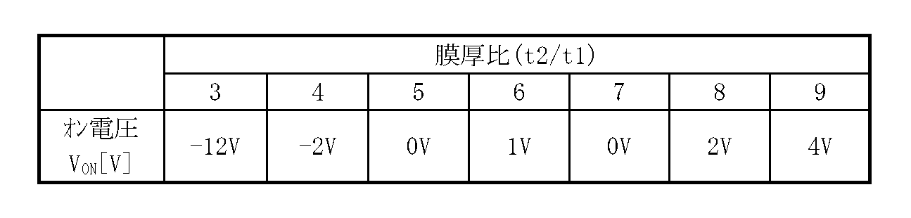
なお、さらに上記のように第1半導体層23Aを非晶質層とした場合、半導体層23のキャリア密度の上昇を防ぎつつ、低キャリア濃度を実現することができる。
Further, when the first semiconductor layer 23A is an amorphous layer as described above, it is possible to realize a low carrier concentration while preventing an increase in the carrier density of the semiconductor layer 23.
なお、第1半導体層23Aおよび第2半導体層23Bの構成材料としては、上記酸化物半導体材料の他に、窒化物半導体材料や酸窒化物半導体材料も用いることができる。窒化物半導体材料を用いて第1半導体層23Aおよび第2半導体層23Bを形成する場合には、酸素欠損生成エネルギーEVOに代えて、窒素欠損生成エネルギーEVNを指標として用いる。即ち、第2半導体層23Bは、第1半導体層23AのEVNの値よりも大きなEVNの値(例えば、EVN>2.3eV)を有する窒化物半導体材料を含んで形成することができる。窒素欠損生成エネルギーEVNは、上述した酸素欠損生成エネルギーEVOの算出方法における酸素原子を窒素原子に置き換えることで同様に算出することができる。
As the constituent materials of the first semiconductor layer 23A and the second semiconductor layer 23B, a nitride semiconductor material or an oxynitride semiconductor material can be used in addition to the oxide semiconductor material. When the first semiconductor layer 23A and the second semiconductor layer 23B are formed by using the nitride semiconductor material, the nitrogen deficiency generation energy EVN is used as an index instead of the oxygen deficiency generation energy EVO. That is, the second semiconductor layer 23B may be formed to include a nitride semiconductor material having a large value of E VN than the value of E VN of the first semiconductor layer 23A (eg, E VN> 2.3 eV) .. The nitrogen deficiency generation energy EVN can be similarly calculated by replacing the oxygen atom with the nitrogen atom in the above-mentioned calculation method of the oxygen deficiency generation energy EVO.
光電変換層24は、光エネルギーを電気エネルギーに変換するためのものである。光電変換層24は、例えば、それぞれp型半導体またはn型半導体として機能する有機材料(p型半導体材料またはn型半導体材料)を2種以上含んで構成されている。光電変換層24は、層内に、p型半導体材料とn型半導体材料との接合面(p/n接合面)を有する。p型半導体は、相対的に電子供与体(ドナー)として機能するものであり、n型半導体は、相対的に電子受容体(アクセプタ)として機能するものである。光電変換層24は、光を吸収した際に生じる励起子が電子と正孔とに分離する場を提供するものであり、具体的には、電子供与体と電子受容体との界面(p/n接合面)において、励起子が電子と正孔とに分離する。
The photoelectric conversion layer 24 is for converting light energy into electrical energy. The photoelectric conversion layer 24 is composed of, for example, two or more types of organic materials (p-type semiconductor materials or n-type semiconductor materials) that function as p-type semiconductors or n-type semiconductors, respectively. The photoelectric conversion layer 24 has a bonding surface (p / n bonding surface) between the p-type semiconductor material and the n-type semiconductor material in the layer. The p-type semiconductor functions relatively as an electron donor (donor), and the n-type semiconductor functions relatively as an electron acceptor (acceptor). The photoelectric conversion layer 24 provides a place where excitons generated when light is absorbed are separated into electrons and holes. Specifically, the interface between the electron donor and the electron acceptor (p /). At the n junction surface), excitons separate into electrons and holes.
光電変換層24は、p型半導体材料およびn型半導体材料の他に、所定の波長域の光を光電変換する一方、他の波長域の光を透過させる有機材料、いわゆる色素材料を含んで構成されていてもよい。光電変換層24をp型半導体材料、n型半導体材料および色素材料の3種類の有機材料を用いて形成する場合には、p型半導体材料およびn型半導体材料は、可視領域(例えば、450nm~800nm)において光透過性を有する材料であることが好ましい。光電変換層24の厚みは、例えば、50nm以上500nm以下である。
The photoelectric conversion layer 24 includes, in addition to the p-type semiconductor material and the n-type semiconductor material, an organic material that photoelectrically converts light in a predetermined wavelength range while transmitting light in another wavelength range, that is, a so-called dye material. It may have been done. When the photoelectric conversion layer 24 is formed using three types of organic materials, a p-type semiconductor material, an n-type semiconductor material, and a dye material, the p-type semiconductor material and the n-type semiconductor material are in the visible region (for example, from 450 nm). It is preferable that the material has light transmission at 800 nm). The thickness of the photoelectric conversion layer 24 is, for example, 50 nm or more and 500 nm or less.
本実施の形態の光電変換層24は、有機材料を含み、可視光から近赤外光の間に吸収を有することが好ましい。光電変換層24を構成する有機材料としては、例えば、キナクリドン誘導体、ナフタレン誘導体、アントラセン誘導体、フェナントレン誘導体、テトラセン誘導体、ピレン誘導体、ペリレン誘導体およびフルオランテン誘導体が挙げられる。光電変換層24は、上記有機材料を2種以上組み合わせて構成されている。上記有機材料は、その組み合わせによってp型半導体またはn型半導体として機能する。
It is preferable that the photoelectric conversion layer 24 of the present embodiment contains an organic material and has absorption between visible light and near infrared light. Examples of the organic material constituting the photoelectric conversion layer 24 include quinacridone derivatives, naphthalene derivatives, anthracene derivatives, phenanthrene derivatives, tetracene derivatives, pyrene derivatives, perylene derivatives and fluoranthene derivatives. The photoelectric conversion layer 24 is composed of a combination of two or more of the above organic materials. The organic material functions as a p-type semiconductor or an n-type semiconductor depending on the combination thereof.
なお、光電変換層24を構成する有機材料は特に限定されない。上記した有機材料以外には、例えば、フェニレンビニレン、フルオレン、カルバゾール、インドール、ピレン、ピロール、ピコリン、チオフェン、アセチレンおよびジアセチレン等の重合体あるいはその誘導体を用いることができる。または、金属錯体色素、シアニン系色素、メロシアニン系色素、フェニルキサンテン系色素、トリフェニルメタン系色素、ロダシアニン系色素、キサンテン系色素、大環状アザアヌレン系色素、アズレン系色素、ナフトキノン系色素、アントラキノン系色素、ピレン等の縮合多環芳香族、芳香環または複素環化合物が縮合した鎖状化合物、スクアリリウム基およびクロコニツクメチン基を結合鎖として有するキノリン、ベンゾチアゾール、ベンゾオキサゾール等の2つの含窒素複素環あるいはスクアリリウム基およびクロコニツクメチン基により結合したシアニン系類似の色素等を用いることができる。なお、金属錯体色素としては、ジチオール金属錯体系色素、金属フタロシアニン色素、金属ポルフィリン色素あるいはルテニウム錯体色素が挙げられる。これらのうち、ルテニウム錯体色素が特に好ましいが、上記に限定するものではない。
The organic material constituting the photoelectric conversion layer 24 is not particularly limited. In addition to the above-mentioned organic materials, for example, polymers such as phenylene vinylene, fluorene, carbazole, indole, pyrrole, pyrrole, picolin, thiophene, acetylene and diacetylene or derivatives thereof can be used. Alternatively, metal complex dyes, cyanine dyes, merocyanine dyes, phenylxanthene dyes, triphenylmethane dyes, rodacyanine dyes, xanthene dyes, macrocyclic azaanulene dyes, azulene dyes, naphthoquinone dyes, anthraquinone dyes. , Pyrene and other condensed polycyclic aromatic compounds, chain compounds fused with aromatic rings or heterocyclic compounds, and two nitrogen-containing heterocycles such as quinoline, benzothiazole, and benzoxanthene having a squarylium group and a croconitecmethine group as bonding chains. Alternatively, a cyanine-based dye or the like bonded by a squarylium group and a croconitecmethine group can be used. Examples of the metal complex dye include a dithiol metal complex dye, a metal phthalocyanine dye, a metal porphyrin dye, and a ruthenium complex dye. Of these, ruthenium complex dyes are particularly preferable, but are not limited to the above.
上部電極25は、下部電極21と同様に光透過性を有する導電膜により構成され、例えば、ITOにより構成されている。上部電極25の構成材料としては、このITOの他にも、ドーパントを添加した酸化スズ(SnO2)系材料、あるいは亜鉛酸化物(ZnO)にドーパントを添加してなる酸化亜鉛系材料を用いてもよい。酸化亜鉛系材料としては、例えば、ドーパントとしてアルミニウム(Al)を添加したアルミニウム亜鉛酸化物(AZO)、ガリウム(Ga)を添加したガリウム亜鉛酸化物(GZO)、インジウム(In)を添加したインジウム亜鉛酸化物(IZO)が挙げられる。また、この他にも、IGZO、ITZO、CuI、InSbO4、ZnMgO、CuInO2、MgIN2O4、CdO、ZnSnO3等を用いてもよい。上部電極25は、単位画素P毎に分離されていてもよいし、各単位画素Pに共通の電極として形成されていてもよい。上部電極25の厚みは、例えば、10nm以上200nm以下である。
The upper electrode 25 is made of a conductive film having light transmission like the lower electrode 21, and is made of, for example, ITO. As the constituent material of the upper electrode 25, in addition to this ITO, a tin oxide (SnO 2 ) -based material to which a dopant is added or a zinc oxide-based material obtained by adding a dopant to zinc oxide (ZnO) is used. May be good. Examples of the zinc oxide-based material include aluminum zinc oxide (AZO) to which aluminum (Al) is added as a dopant, gallium zinc oxide (GZO) to which gallium (Ga) is added, and indium zinc to which indium (In) is added. Oxide (IZO) can be mentioned. Also, the addition to, IGZO, ITZO, CuI, InSbO 4, ZnMgO, CuInO 2, MgIN 2 O 4, CdO, may be used ZnSnO 3, and the like. The upper electrode 25 may be separated for each unit pixel P, or may be formed as an electrode common to each unit pixel P. The thickness of the upper electrode 25 is, for example, 10 nm or more and 200 nm or less.
なお、光電変換層24と下部電極21との間(例えば、半導体層23と光電変換層24との間)および光電変換層24と上部電極25との間には、他の層が設けられていてもよい。例えば、下部電極21側から順に、半導体層23、電子ブロッキング膜を兼ねるバッファ層、光電変換層24、正孔ブロッキング膜を兼ねるバッファ層および仕事関数調整層等が積層されていてもよい。また、光電変換層24は、例えば、p型ブロッキング層、p型半導体およびn型半導体を含む層(i層)およびn型ブロッキング層が積層されたpinバルクヘテロ構造としてもよい。
Other layers are provided between the photoelectric conversion layer 24 and the lower electrode 21 (for example, between the semiconductor layer 23 and the photoelectric conversion layer 24) and between the photoelectric conversion layer 24 and the upper electrode 25. You may. For example, the semiconductor layer 23, the buffer layer also serving as an electron blocking film, the photoelectric conversion layer 24, the buffer layer also serving as a hole blocking film, the work function adjusting layer, and the like may be laminated in this order from the lower electrode 21 side. Further, the photoelectric conversion layer 24 may have, for example, a pin bulk heterostructure in which a p-type blocking layer, a layer (i layer) containing a p-type semiconductor and an n-type semiconductor, and an n-type blocking layer are laminated.
絶縁層26は、半導体基板30の第1面30Aを覆い、半導体基板30との界面準位を低減させると共に、半導体基板30との界面からの暗電流の発生を抑制するためのものである。また、絶縁層26は、半導体基板30の第1面30Aから第2面30Bを貫通する貫通電極34が形成される開口34H(図14参照)の側面に亘って延在している。絶縁層26は、例えば、固定電荷層26Aと誘電体層26Bとの積層構造を有している。
The insulating layer 26 covers the first surface 30A of the semiconductor substrate 30, reduces the interface state with the semiconductor substrate 30, and suppresses the generation of dark current from the interface with the semiconductor substrate 30. Further, the insulating layer 26 extends from the first surface 30A of the semiconductor substrate 30 to the side surface of the opening 34H (see FIG. 14) in which the through electrodes 34 penetrating the second surface 30B are formed. The insulating layer 26 has, for example, a laminated structure of a fixed charge layer 26A and a dielectric layer 26B.
固定電荷層26Aは、正の固定電荷を有する膜でもよいし、負の固定電荷を有する膜でもよい。固定電荷層26Aの構成材料としては、半導体基板30よりもバンドギャップの広い半導体材料または導電材料を用いて形成することが好ましい。これにより、半導体基板30の界面における暗電流の発生を抑えることができる。固定電荷層26Aの構成材料としては、例えば、酸化ハフニウム(HfOx)、酸化アルミニウム(AlOx)、酸化ジルコニウム(ZrOx)、酸化タンタル(TaOx)、酸化チタン(TiOx)、酸化ランタン(LaOx)、酸化プラセオジム(PrOx)、酸化セリウム(CeOx)、酸化ネオジム(NdOx)、酸化プロメチウム(PmOx)、酸化サマリウム(SmOx)、酸化ユウロピウム(EuOx)、酸化ガドリニウム(GdOx)、酸化テルビウム(TbOx)、酸化ジスプロシウム(DyOx)、酸化ホルミウム(HoOx)、酸化ツリウム(TmOx)、酸化イッテルビウム(YbOx)、酸化ルテチウム(LuOx)、酸化イットリウム(YOx)、窒化ハフニウム(HfNx)、窒化アルミニウム(AlNx)、酸窒化ハフニウム(HfOxNy)および酸窒化アルミニウム(AlOxNy)等が挙げられる。
The fixed charge layer 26A may be a film having a positive fixed charge or a film having a negative fixed charge. As the constituent material of the fixed charge layer 26A, it is preferable to use a semiconductor material or a conductive material having a bandgap wider than that of the semiconductor substrate 30. As a result, it is possible to suppress the generation of dark current at the interface of the semiconductor substrate 30. Examples of the constituent materials of the fixed charge layer 26A include hafnium oxide (HfO x ), aluminum oxide (AlO x ), zirconium oxide (ZrO x ), tantalum oxide (TaO x ), titanium oxide (TIO x ), and lanthanum oxide (Tio x). LaO x ), placeodymium oxide (PrO x ), cerium oxide (CeO x ), neodymium oxide (NdO x ), promethium oxide (PmO x ), samarium oxide (SmO x ), europium oxide (EuO x ), gadolinium oxide (GdO) x), terbium oxide (TBO x), dysprosium oxide (DyO x), holmium oxide (HoO x), thulium oxide (TMO x), ytterbium oxide (YbO x), lutetium oxide (LuO x), yttrium oxide (YO x ), Hafnium nitride (HfN x ), aluminum nitride (AlN x ), hafnium oxynitride (HfO x N y ), aluminum oxynitride (AlO x N y ) and the like.
誘電体層26Bは、半導体基板30と層間絶縁層27との間の屈折率差によって生じる光の反射を防止するためのものである。誘電体層26Bの構成材料としては、半導体基板30の屈折率と層間絶縁層27の屈折率との間の屈折率を有する材料であることが好ましい。誘電体層26Bの構成材料としては、例えば、酸化シリコン、TEOS、窒化シリコンおよび酸窒化シリコン(SiON)等が挙げられる。
The dielectric layer 26B is for preventing the reflection of light caused by the difference in refractive index between the semiconductor substrate 30 and the interlayer insulating layer 27. The constituent material of the dielectric layer 26B is preferably a material having a refractive index between the refractive index of the semiconductor substrate 30 and the refractive index of the interlayer insulating layer 27. Examples of the constituent material of the dielectric layer 26B include silicon oxide, TEOS, silicon nitride, silicon oxynitride (SiON) and the like.
層間絶縁層27は、例えば、酸化シリコン、窒化シリコンおよび酸窒化シリコン等のうちの1種よりなる単層膜か、あるいはこれらのうちの2種以上よりなる積層膜により構成されている。
The interlayer insulating layer 27 is composed of, for example, a single-layer film made of one of silicon oxide, silicon nitride, silicon oxynitride, and the like, or a laminated film made of two or more of these.
図1には示していないが、層間絶縁層27上には、下部電極21と共に、シールド電極28が設けられている。シールド電極28は、隣り合う画素ユニット1a間における容量結合を防ぐためのものであり、例えば、2行×2列で配置された4つの単位画素Pからなる画素ユニット1aの周囲に設けられ、固定電位が印加されている。シールド電極28は、さらに、画素ユニット1a内において、行方向(Z軸方向)および列方向(X軸方向)に隣り合う単位画素P間に延在している。
Although not shown in FIG. 1, a shield electrode 28 is provided on the interlayer insulating layer 27 together with a lower electrode 21. The shield electrode 28 is for preventing capacitive coupling between adjacent pixel units 1a. For example, the shield electrode 28 is provided and fixed around a pixel unit 1a composed of four unit pixels P arranged in 2 rows × 2 columns. An electric potential is applied. The shield electrode 28 further extends in the pixel unit 1a between unit pixels P adjacent to each other in the row direction (Z-axis direction) and the column direction (X-axis direction).
半導体基板30は、例えば、n型のシリコン(Si)基板により構成され、所定の領域にpウェル31を有している。
The semiconductor substrate 30 is composed of, for example, an n-type silicon (Si) substrate, and has a p-well 31 in a predetermined region.
無機光電変換部32B,32Rは、それぞれ、半導体基板30の所定の領域にpn接合を有するフォトダイオード(PD)によって構成され、Si基板において光の入射深さに応じて吸収される光の波長が異なることを利用して縦方向に光を分光することを可能としたものである。無機光電変換部32Bは、青色光を選択的に検出して青色に対応する信号電荷を蓄積させるものであり、青色光を効率的に光電変換可能な深さに設置されている。無機光電変換部32Rは、赤色光を選択的に検出して赤色に対応する信号電荷を蓄積させるものであり、赤色光を効率的に光電変換可能な深さに設置されている。なお、青(B)は、例えば450nm以上495nm以下の波長域、赤(R)は、例えば620nm以上750nm以下の波長域にそれぞれ対応する色である。無機光電変換部32B,32Rはそれぞれ、各波長域のうちの一部または全部の波長域の光を検出可能となっていればよい。
The inorganic photoelectric conversion units 32B and 32R are each composed of a photodiode (PD) having a pn junction in a predetermined region of the semiconductor substrate 30, and the wavelength of light absorbed by the Si substrate according to the incident depth of light is set. It is possible to disperse light in the vertical direction by utilizing different things. The inorganic photoelectric conversion unit 32B selectively detects blue light and accumulates a signal charge corresponding to blue light, and is installed at a depth at which blue light can be efficiently photoelectrically converted. The inorganic photoelectric conversion unit 32R selectively detects red light and accumulates a signal charge corresponding to red, and is installed at a depth at which red light can be efficiently photoelectrically converted. Blue (B) is, for example, a color corresponding to a wavelength range of 450 nm or more and 495 nm or less, and red (R) is a color corresponding to, for example, a wavelength range of 620 nm or more and 750 nm or less. It suffices that the inorganic photoelectric conversion units 32B and 32R can detect light in a part or all of each wavelength range, respectively.
無機光電変換部32Bは、例えば、正孔蓄積層となるp+領域と、電子蓄積層となるn領域とを含んで構成されている。無機光電変換部32Rは、例えば、正孔蓄積層となるp+領域と、電子蓄積層となるn領域とを有する(p-n-pの積層構造を有する)。無機光電変換部32Bのn領域は、縦型の転送トランジスタTr2に接続されている。無機光電変換部32Bのp+領域は、転送トランジスタTr2に沿って屈曲し、無機光電変換部32Rのp+領域につながっている。
The inorganic photoelectric conversion unit 32B includes, for example, a p + region serving as a hole storage layer and an n region serving as an electron storage layer. The inorganic photoelectric conversion unit 32R has, for example, a p + region serving as a hole storage layer and an n region serving as an electron storage layer (having a pn-p laminated structure). The n region of the inorganic photoelectric conversion unit 32B is connected to the vertical transfer transistor Tr2. The p + region of the inorganic photoelectric conversion unit 32B is bent along the transfer transistor Tr2 and is connected to the p + region of the inorganic photoelectric conversion unit 32R.
ゲート絶縁層33は、例えば、酸化シリコン、窒化シリコンおよび酸窒化シリコン等のうちの1種よりなる単層膜か、あるいはこれらのうちの2種以上よりなる積層膜により構成されている。
The gate insulating layer 33 is composed of, for example, a single-layer film made of one of silicon oxide, silicon nitride, silicon oxynitride, and the like, or a laminated film made of two or more of these.
貫通電極34は、半導体基板30の第1面30Aと第2面30Bとの間に設けられ、有機光電変換部20とアンプトランジスタAMPのゲートGampおよびフローティングディフュージョンFD1とのコネクタとしての機能を有すると共に、有機光電変換部20において生じた電荷の伝送経路となるものである。フローティングディフュージョンFD1(リセットトランジスタRSTの一方のソース/ドレイン領域36B)の隣にはリセットトランジスタRSTのリセットゲートGrstが配置されている。これにより、フローティングディフュージョンFD1に蓄積された電荷を、リセットトランジスタRSTによりリセットすることが可能となる。
The through electrode 34 is provided between the first surface 30A and the second surface 30B of the semiconductor substrate 30, and has a function as a connector between the organic photoelectric conversion unit 20 and the gate Gamp and the floating diffusion FD1 of the amplifier transistor AMP. , It serves as a transmission path for the electric charge generated in the organic photoelectric conversion unit 20. The reset gate Grst of the reset transistor RST is arranged next to the floating diffusion FD1 (one source / drain region 36B of the reset transistor RST). As a result, the electric charge accumulated in the floating diffusion FD1 can be reset by the reset transistor RST.
パッド部39A,39B、上部第1コンタクト39C、上部第2コンタクト39D、下部第1コンタクト45、下部第2コンタクト46および配線52は、例えば、PDAS(Phosphorus Doped Amorphous Silicon)等のドープされたシリコン材料、または、アルミニウム(Al)、タングステン(W)、チタン(Ti)、コバルト(Co)、ハフニウム(Hf)およびタンタル(Ta)等の金属材料を用いて形成することができる。
The pad portions 39A and 39B, the upper first contact 39C, the upper second contact 39D, the lower first contact 45, the lower second contact 46 and the wiring 52 are made of a doped silicon material such as PDAS (Phosphorus Doped Amorphous Silicon). Alternatively, it can be formed using a metal material such as aluminum (Al), tungsten (W), titanium (Ti), cobalt (Co), hafnium (Hf) and tantalum (Ta).
保護層51およびオンチップレンズ54は、光透過性を有する材料により構成され、例えば、酸化シリコン、窒化シリコンおよび酸窒化シリコン等のうちのいずれかよりなる単層膜、あるいはそれらのうちの2種以上よりなる積層膜により構成されている。この保護層51の厚みは、例えば、100nm以上30000nm以下である。
The protective layer 51 and the on-chip lens 54 are made of a light-transmitting material, for example, a single-layer film made of silicon oxide, silicon nitride, silicon oxynitride, or the like, or two of them. It is composed of the above-mentioned laminated film. The thickness of the protective layer 51 is, for example, 100 nm or more and 30,000 nm or less.
遮光膜53は、例えば、配線52と共に保護層51内に、少なくとも蓄積電極21Bにはかからず、半導体層23と直接接している読み出し電極21Aの領域を覆うように設けられている。遮光膜53は、例えば、タングステン(W)、アルミニウム(Al)およびAlと銅(Cu)との合金等を用いて形成することができる。
For example, the light-shielding film 53 is provided in the protective layer 51 together with the wiring 52 so as to cover the region of the readout electrode 21A which is in direct contact with the semiconductor layer 23 without covering at least the storage electrode 21B. The light-shielding film 53 can be formed by using, for example, tungsten (W), aluminum (Al), an alloy of Al and copper (Cu), or the like.
図11は、図1に示した撮像素子10の等価回路図である。図12は、図1に示した撮像素子10の下部電極21および制御部を構成するトランジスタの配置を模式的に表したものである。
FIG. 11 is an equivalent circuit diagram of the image pickup device 10 shown in FIG. FIG. 12 schematically shows the arrangement of the lower electrode 21 of the image pickup device 10 shown in FIG. 1 and the transistors constituting the control unit.
リセットトランジスタRST(リセットトランジスタTR1rst)は、有機光電変換部20からフローティングディフュージョンFD1に転送された電荷をリセットするためのものであり、例えばMOSトランジスタにより構成されている。具体的には、リセットトランジスタTR1rstは、リセットゲートGrstと、チャネル形成領域36Aと、ソース/ドレイン領域36B,36Cとから構成されている。リセットゲートGrstは、リセット線RST1に接続され、リセットトランジスタTR1rstの一方のソース/ドレイン領域36Bは、フローティングディフュージョンFD1を兼ねている。リセットトランジスタTR1rstを構成する他方のソース/ドレイン領域36Cは、電源線VDDに接続されている。
The reset transistor RST (reset transistor TR1rst) is for resetting the electric charge transferred from the organic photoelectric conversion unit 20 to the floating diffusion FD1, and is composed of, for example, a MOS transistor. Specifically, the reset transistor TR1rst is composed of a reset gate Grst, a channel forming region 36A, and source / drain regions 36B and 36C. The reset gate Grst is connected to the reset line RST1, and one source / drain region 36B of the reset transistor TR1rst also serves as a floating diffusion FD1. The other source / drain region 36C constituting the reset transistor TR1rst is connected to the power supply line VDD.
アンプトランジスタAMPは、有機光電変換部20で生じた電荷量を電圧に変調する変調素子であり、例えばMOSトランジスタにより構成されている。具体的には、アンプトランジスタAMPは、ゲートGampと、チャネル形成領域35Aと、ソース/ドレイン領域35B,35Cとから構成されている。ゲートGampは、下部第1コンタクト45、接続部41A、下部第2コンタクト46および貫通電極34等を介して、読み出し電極21AおよびリセットトランジスタTR1rstの一方のソース/ドレイン領域36B(フローティングディフュージョンFD1)に接続されている。また、一方のソース/ドレイン領域35Bは、リセットトランジスタTR1rstを構成する他方のソース/ドレイン領域36Cと、領域を共有しており、電源線VDDに接続されている。
The amplifier transistor AMP is a modulation element that modulates the amount of electric charge generated by the organic photoelectric conversion unit 20 into a voltage, and is composed of, for example, a MOS transistor. Specifically, the amplifier transistor AMP is composed of a gate Gamp, a channel forming region 35A, and source / drain regions 35B and 35C. The gate Gamp is connected to one source / drain region 36B (floating diffusion FD1) of the read electrode 21A and the reset transistor TR1rst via the lower first contact 45, the connecting portion 41A, the lower second contact 46, the through electrode 34, and the like. Has been done. Further, one source / drain region 35B shares an region with the other source / drain region 36C constituting the reset transistor TR1rst, and is connected to the power supply line VDD.
選択トランジスタSEL(選択トランジスタTR1sel)は、ゲートGselと、チャネル形成領域34Aと、ソース/ドレイン領域34B,34Cとから構成されている。ゲートGselは、選択線SEL1に接続されている。一方のソース/ドレイン領域34Bは、アンプトランジスタAMPを構成する他方のソース/ドレイン領域35Cと、領域を共有しており、他方のソース/ドレイン領域34Cは、信号線(データ出力線)VSL1に接続されている。
The selection transistor SEL (selection transistor TR1sel) is composed of a gate Gsel, a channel formation region 34A, and source / drain regions 34B and 34C. The gate Gsel is connected to the selection line SEL1. One source / drain region 34B shares an area with the other source / drain region 35C constituting the amplifier transistor AMP, and the other source / drain region 34C is connected to the signal line (data output line) VSL1. Has been done.
転送トランジスタTR2(転送トランジスタTR2trs)は、無機光電変換部32Bにおいて発生し、蓄積された、青色に対応する信号電荷を、フローティングディフュージョンFD2に転送するためのものである。無機光電変換部32Bは半導体基板30の第2面30Bから深い位置に形成されているので、無機光電変換部32Bの転送トランジスタTR2trsは縦型のトランジスタにより構成されていることが好ましい。転送トランジスタTR2trsは、転送ゲート線TG2に接続されている。転送トランジスタTR2trsのゲートGtrs2の近傍の領域37Cには、フローティングディフュージョンFD2が設けられている。無機光電変換部32Bに蓄積された電荷は、ゲートGtrs2に沿って形成される転送チャネルを介してフローティングディフュージョンFD2に読み出される。
The transfer transistor TR2 (transfer transistor TR2trs) is for transferring the signal charge corresponding to the blue color generated and accumulated in the inorganic photoelectric conversion unit 32B to the floating diffusion FD2. Since the inorganic photoelectric conversion unit 32B is formed at a position deep from the second surface 30B of the semiconductor substrate 30, it is preferable that the transfer transistor TR2trs of the inorganic photoelectric conversion unit 32B is composed of a vertical transistor. The transfer transistor TR2trs is connected to the transfer gate line TG2. A floating diffusion FD2 is provided in a region 37C near the gate Gtrs2 of the transfer transistor TR2trs. The charge accumulated in the inorganic photoelectric conversion unit 32B is read out to the floating diffusion FD2 via a transfer channel formed along the gate Gtrs2.
転送トランジスタTR3(転送トランジスタTR3trs)は、無機光電変換部32Rにおいて発生し、蓄積された赤色に対応する信号電荷を、フローティングディフュージョンFD3に転送するためのものであり、例えばMOSトランジスタにより構成されている。転送トランジスタTR3trsは、転送ゲート線TG3に接続されている。転送トランジスタTR3trsのゲートGtrs3の近傍の領域38Cには、フローティングディフュージョンFD3が設けられている。無機光電変換部32Rに蓄積された電荷は、ゲートGtrs3に沿って形成される転送チャネルを介してフローティングディフュージョンFD3に読み出される。
The transfer transistor TR3 (transfer transistor TR3trs) is for transferring the signal charge corresponding to the accumulated red color generated in the inorganic photoelectric conversion unit 32R to the floating diffusion FD3, and is composed of, for example, a MOS transistor. .. The transfer transistor TR3trs is connected to the transfer gate line TG3. A floating diffusion FD3 is provided in the region 38C near the gate Gtrs3 of the transfer transistor TR3trs. The charge accumulated in the inorganic photoelectric conversion unit 32R is read out to the floating diffusion FD3 via a transfer channel formed along the gate Gtrs3.
半導体基板30の第2面30B側には、さらに、無機光電変換部32Bの制御部を構成するリセットトランジスタTR2rstと、アンプトランジスタTR2ampと、選択トランジスタTR2selが設けられている。更に、無機光電変換部32Rの制御部を構成するリセットトランジスタTR3rstと、アンプトランジスタTR3ampおよび選択トランジスタTR3selが設けられている。
On the second surface 30B side of the semiconductor substrate 30, a reset transistor TR2rst, an amplifier transistor TR2amp, and a selection transistor TR2sel that form a control unit of the inorganic photoelectric conversion unit 32B are further provided. Further, a reset transistor TR3rst, an amplifier transistor TR3amp, and a selection transistor TR3sel, which form a control unit of the inorganic photoelectric conversion unit 32R, are provided.
リセットトランジスタTR2rstは、ゲート、チャネル形成領域およびソース/ドレイン領域から構成されている。リセットトランジスタTR2rstのゲートはリセット線RST2に接続され、リセットトランジスタTR2rstの一方のソース/ドレイン領域は電源線VDDに接続されている。リセットトランジスタTR2rstの他方のソース/ドレイン領域は、フローティングディフュージョンFD2を兼ねている。
The reset transistor TR2rst is composed of a gate, a channel forming region, and a source / drain region. The gate of the reset transistor TR2rst is connected to the reset line RST2, and one source / drain region of the reset transistor TR2rst is connected to the power supply line VDD. The other source / drain region of the reset transistor TR2rst also serves as a floating diffusion FD2.
アンプトランジスタTR2ampは、ゲート、チャネル形成領域およびソース/ドレイン領域から構成されている。ゲートは、リセットトランジスタTR2rstの他方のソース/ドレイン領域(フローティングディフュージョンFD2)に接続されている。アンプトランジスタTR2ampを構成する一方のソース/ドレイン領域は、リセットトランジスタTR2rstを構成する一方のソース/ドレイン領域と領域を共有しており、電源線VDDに接続されている。
The amplifier transistor TR2amp is composed of a gate, a channel forming region, and a source / drain region. The gate is connected to the other source / drain region (floating diffusion FD2) of the reset transistor TR2rst. One source / drain region constituting the amplifier transistor TR2amp shares an region with one source / drain region constituting the reset transistor TR2rst, and is connected to the power supply line VDD.
選択トランジスタTR2selは、ゲート、チャネル形成領域およびソース/ドレイン領域から構成されている。ゲートは、選択線SEL2に接続されている。選択トランジスタTR2selを構成する一方のソース/ドレイン領域は、アンプトランジスタTR2ampを構成する他方のソース/ドレイン領域と領域を共有している。選択トランジスタTR2selを構成する他方のソース/ドレイン領域は、信号線(データ出力線)VSL2に接続されている。
The selection transistor TR2sel is composed of a gate, a channel forming region, and a source / drain region. The gate is connected to the selection line SEL2. One source / drain region constituting the selection transistor TR2sel shares an region with the other source / drain region constituting the amplifier transistor TR2amp. The other source / drain region constituting the selection transistor TR2sel is connected to the signal line (data output line) VSL2.
リセットトランジスタTR3rstは、ゲート、チャネル形成領域およびソース/ドレイン領域から構成されている。リセットトランジスタTR3rstのゲートはリセット線RST3に接続され、リセットトランジスタTR3rstを構成する一方のソース/ドレイン領域は電源線VDDに接続されている。リセットトランジスタTR3rstを構成する他方のソース/ドレイン領域は、フローティングディフュージョンFD3を兼ねている。
The reset transistor TR3rst is composed of a gate, a channel forming region, and a source / drain region. The gate of the reset transistor TR3rst is connected to the reset line RST3, and one source / drain region constituting the reset transistor TR3rst is connected to the power supply line VDD. The other source / drain region constituting the reset transistor TR3rst also serves as a floating diffusion FD3.
アンプトランジスタTR3ampは、ゲート、チャネル形成領域およびソース/ドレイン領域から構成されている。ゲートは、リセットトランジスタTR3rstを構成する他方のソース/ドレイン領域(フローティングディフュージョンFD3)に接続されている。アンプトランジスタTR3ampを構成する一方のソース/ドレイン領域は、リセットトランジスタTR3rstを構成する一方のソース/ドレイン領域と、領域を共有しており、電源線VDDに接続されている。
The amplifier transistor TR3amp is composed of a gate, a channel forming region, and a source / drain region. The gate is connected to the other source / drain region (floating diffusion FD3) constituting the reset transistor TR3rst. One source / drain region constituting the amplifier transistor TR3amp shares an region with one source / drain region constituting the reset transistor TR3rst, and is connected to the power supply line VDD.
選択トランジスタTR3selは、ゲート、チャネル形成領域およびソース/ドレイン領域から構成されている。ゲートは、選択線SEL3に接続されている。選択トランジスタTR3selを構成する一方のソース/ドレイン領域は、アンプトランジスタTR3ampを構成する他方のソース/ドレイン領域と、領域を共有している。選択トランジスタTR3selを構成する他方のソース/ドレイン領域は、信号線(データ出力線)VSL3に接続されている。
The selection transistor TR3sel is composed of a gate, a channel forming region, and a source / drain region. The gate is connected to the selection line SEL3. One source / drain region constituting the selection transistor TR3sel shares an region with the other source / drain region constituting the amplifier transistor TR3amp. The other source / drain region constituting the selection transistor TR3sel is connected to the signal line (data output line) VSL3.
リセット線RST1,RST2,RST3、選択線SEL1,SEL2,SEL3、転送ゲート線TG2,TG3は、それぞれ、駆動回路を構成する垂直駆動回路に接続されている。信号線(データ出力線)VSL1,VSL2,VSL3は、駆動回路を構成するカラム信号処理回路113に接続されている。
The reset lines RST1, RST2, RST3, selection lines SEL1, SEL2, SEL3, and transfer gate lines TG2, TG3 are each connected to a vertical drive circuit constituting the drive circuit. The signal lines (data output lines) VSL1, VSL2, and VSL3 are connected to the column signal processing circuit 113 constituting the drive circuit.
(1-2.撮像素子の製造方法)
本実施の形態の撮像素子10は、例えば、次のようにして製造することができる。 (1-2. Manufacturing method of image sensor)
Theimage sensor 10 of the present embodiment can be manufactured, for example, as follows.
本実施の形態の撮像素子10は、例えば、次のようにして製造することができる。 (1-2. Manufacturing method of image sensor)
The
図13~図18は、撮像素子10の製造方法を工程順に表したものである。まず、図13に示したように、半導体基板30内に例えばpウェル31を形成し、このpウェル31内に例えばn型の無機光電変換部32B,32Rを形成する。半導体基板30の第1面30A近傍にはp+領域を形成する。
13 to 18 show the manufacturing method of the image sensor 10 in the order of processes. First, as shown in FIG. 13, for example, a p-well 31 is formed in the semiconductor substrate 30, and for example, n-type inorganic photoelectric conversion units 32B and 32R are formed in the p-well 31. A p + region is formed in the vicinity of the first surface 30A of the semiconductor substrate 30.
半導体基板30の第2面30Bには、同じく図13に示したように、例えばフローティングディフュージョンFD1~FD3となるn+領域を形成したのち、ゲート絶縁層33と、転送トランジスタTr2、転送トランジスタTr3、選択トランジスタSEL、アンプトランジスタAMPおよびリセットトランジスタRSTの各ゲートを含むゲート配線層47とを形成する。これにより、転送トランジスタTr2、転送トランジスタTr3、選択トランジスタSEL、アンプトランジスタAMPおよびリセットトランジスタRSTを形成する。更に、半導体基板30の第2面30B上に、下部第1コンタクト45、下部第2コンタクト46および接続部41Aを含む配線層41~43および絶縁層44からなる多層配線層40を形成する。
As also shown in FIG. 13, the second surface 30B of the semiconductor substrate 30 is formed with an n + region to be, for example, floating diffusion FD1 to FD3, and then the gate insulating layer 33, the transfer transistor Tr2, and the transfer transistor Tr3 are selected. A gate wiring layer 47 including each gate of the transistor SEL, the amplifier transistor AMP, and the reset transistor RST is formed. As a result, the transfer transistor Tr2, the transfer transistor Tr3, the selection transistor SEL, the amplifier transistor AMP, and the reset transistor RST are formed. Further, a multilayer wiring layer 40 composed of wiring layers 41 to 43 including a lower first contact 45, a lower second contact 46, and a connecting portion 41A and an insulating layer 44 is formed on the second surface 30B of the semiconductor substrate 30.
半導体基板30の基体としては、例えば、半導体基板30と、埋込み酸化膜(図示せず)と、保持基板(図示せず)とを積層したSOI(Silicon on Insulator)基板を用いる。埋込み酸化膜および保持基板は、図13には図示しないが、半導体基板30の第1面30Aに接合されている。イオン注入後、アニール処理を行う。
As the substrate of the semiconductor substrate 30, for example, an SOI (Silicon on Insulator) substrate in which a semiconductor substrate 30, an embedded oxide film (not shown), and a holding substrate (not shown) are laminated is used. Although not shown in FIG. 13, the embedded oxide film and the holding substrate are bonded to the first surface 30A of the semiconductor substrate 30. After ion implantation, annealing is performed.
次いで、半導体基板30の第2面30B側に設けられた多層配線層40上に支持基板(図示せず)または他の半導体基体等を接合して、上下反転する。続いて、半導体基板30をSOI基板の埋込み酸化膜および保持基板から分離し、半導体基板30の第1面30Aを露出させる。以上の工程は、イオン注入およびCVD(Chemical Vapor Deposition)法等、通常のCMOSプロセスで使用されている技術にて行うことが可能である。
Next, a support substrate (not shown) or another semiconductor substrate is bonded onto the multilayer wiring layer 40 provided on the second surface 30B side of the semiconductor substrate 30, and the semiconductor substrate 30 is turned upside down. Subsequently, the semiconductor substrate 30 is separated from the embedded oxide film and the holding substrate of the SOI substrate to expose the first surface 30A of the semiconductor substrate 30. The above steps can be performed by techniques used in ordinary CMOS processes, such as ion implantation and CVD (Chemical Vapor Deposition) methods.
次いで、図14に示したように、例えばドライエッチングにより半導体基板30を第1面30A側から加工し、例えば環状の開口34Hを形成する。開口34Hの深さは、図14に示したように、半導体基板30の第1面30Aから第2面30Bまで貫通すると共に、例えば、接続部41Aまで達するものである。
Next, as shown in FIG. 14, the semiconductor substrate 30 is processed from the first surface 30A side by, for example, dry etching to form, for example, an annular opening 34H. As shown in FIG. 14, the depth of the opening 34H penetrates from the first surface 30A to the second surface 30B of the semiconductor substrate 30, and reaches, for example, the connection portion 41A.
続いて、半導体基板30の第1面30Aおよび開口34Hの側面に、例えば負の固定電荷層26Aおよび誘電体層26Bを順に形成する。固定電荷層26Aは、例えば、原子層堆積法(ALD法)を用いて酸化ハフニウム膜や酸化アルミニウム膜を成膜することで形成することができる。誘電体層26Bは、例えば、プラズマCVD法を用いて酸化シリコン膜を製膜することで形成することができる。次に、誘電体層26B上の所定の位置に、例えば、チタンと窒化チタンとの積層膜(Ti/TiN膜)からなるバリアメタルとタングステン膜とが積層されたパッド部39A,39Bを形成する。これにより、パッド部39A,39Bを遮光膜として用いることができる。その後、誘電体層26Bおよびパッド部39A,39B上に、層間絶縁層27を形成し、CMP(Chemical Mechanical Polishing)法を用いて層間絶縁層27の表面を平坦化する。
Subsequently, for example, a negative fixed charge layer 26A and a dielectric layer 26B are sequentially formed on the first surface 30A and the side surface of the opening 34H of the semiconductor substrate 30. The fixed charge layer 26A can be formed, for example, by forming a hafnium oxide film or an aluminum oxide film using an atomic layer deposition method (ALD method). The dielectric layer 26B can be formed, for example, by forming a silicon oxide film using a plasma CVD method. Next, pad portions 39A and 39B in which a barrier metal made of a laminated film of titanium and titanium nitride (Ti / TiN film) and a tungsten film are laminated are formed at predetermined positions on the dielectric layer 26B. .. As a result, the pad portions 39A and 39B can be used as a light-shielding film. After that, the interlayer insulating layer 27 is formed on the dielectric layer 26B and the pad portions 39A and 39B, and the surface of the interlayer insulating layer 27 is flattened by using a CMP (Chemical Mechanical Polishing) method.
続いて、図15に示したように、パッド部39A,39B上に、それぞれ開口27H1,27H2を形成した後、この開口27H1,27H2に、例えばAl等の導電材料を埋め込み、上部第1コンタクト39Cおよび上部第2コンタクト39Dを形成する。
Subsequently, as shown in FIG. 15, after the openings 27H1,27H2 are formed on the pad portions 39A and 39B, respectively, a conductive material such as Al is embedded in the openings 27H1,27H2, and the upper first contact 39C is formed. And the upper second contact 39D is formed.
次に、図16に示したように、層間絶縁層27上に、例えば、スパッタリング法を用いて導電膜21xを成膜した後、フォトリソグラフィー技術を用いてパターニングを行う。具体的には、導電膜21xの所定の位置にフォトレジストPRを形成した後、ドライエッチングまたはウェットエッチングを用いて導電膜21xを加工する。その後、フォトレジストPRを除去することで、図17に示したように、読み出し電極21Aおよび蓄積電極21Bが形成される。
Next, as shown in FIG. 16, a conductive film 21x is formed on the interlayer insulating layer 27 by, for example, a sputtering method, and then patterning is performed using a photolithography technique. Specifically, after forming a photoresist PR at a predetermined position of the conductive film 21x, the conductive film 21x is processed by dry etching or wet etching. After that, by removing the photoresist PR, the readout electrode 21A and the storage electrode 21B are formed as shown in FIG.
続いて、図18に示したように、絶縁層22、第1半導体層23Aおよび第2半導体層23Bからなる半導体層23、光電変換層24および上部電極25を形成する。絶縁層22は、例えば、ALD法を用いて酸化シリコン膜を製膜した後、CMP法を用いて絶縁層22の表面を平坦化する。その後、読み出し電極21A上に、例えば、ウェットエッチングを用いて開口22Hを形成する。半導体層23は、例えば、スパッタリング法を用いて形成することができる。光電変換層24は、例えば、真空蒸着法を用いて形成する。上部電極25は、下部電極21と同様に、例えば、スパッタリング法を用いて形成する。最後に、上部電極25上に、保護層51、配線52、遮光膜53およびオンチップレンズ54を配設する。以上により、図1に示した撮像素子10が完成する。
Subsequently, as shown in FIG. 18, a semiconductor layer 23 composed of an insulating layer 22, a first semiconductor layer 23A and a second semiconductor layer 23B, a photoelectric conversion layer 24, and an upper electrode 25 are formed. For the insulating layer 22, for example, a silicon oxide film is formed by using the ALD method, and then the surface of the insulating layer 22 is flattened by using the CMP method. Then, the opening 22H is formed on the readout electrode 21A by, for example, wet etching. The semiconductor layer 23 can be formed, for example, by using a sputtering method. The photoelectric conversion layer 24 is formed, for example, by using a vacuum vapor deposition method. Like the lower electrode 21, the upper electrode 25 is formed by, for example, a sputtering method. Finally, the protective layer 51, the wiring 52, the light-shielding film 53, and the on-chip lens 54 are arranged on the upper electrode 25. As a result, the image sensor 10 shown in FIG. 1 is completed.
なお、上記のように、半導体層23と光電変換層24との間および光電変換層24と上部電極25との間に、電子ブロッキング膜を兼ねるバッファ層や、正孔ブロッキング膜を兼ねるバッファ層あるいは仕事関数調整層等の有機材料を含む他の層を形成する場合には、各層を真空工程において連続的に(真空一貫プロセスで)形成することが望ましい。また、光電変換層24の成膜方法としては、必ずしも真空蒸着法を用いた手法に限らず、例えば、スピンコート技術やプリント技術等を用いてもよい。更に、透明電極(下部電極21および上部電極25)を形成する方法としては、透明電極を構成する材料にもよるが、真空蒸着法や反応性蒸着法、電子ビーム蒸着法、イオンプレーティング法といった物理的気相成長法(PVD法)、パイロゾル法、有機金属化合物を熱分解する方法、スプレー法、ディップ法、MOCVD法を含む各種の化学的気相成長法(CVD法)、無電解メッキ法および電解メッキ法を挙げることができる。
As described above, between the semiconductor layer 23 and the photoelectric conversion layer 24 and between the photoelectric conversion layer 24 and the upper electrode 25, a buffer layer that also serves as an electron blocking film, a buffer layer that also serves as a hole blocking film, or When forming other layers containing an organic material such as a work function adjusting layer, it is desirable to form each layer continuously (in a vacuum integrated process) in a vacuum process. Further, the film forming method of the photoelectric conversion layer 24 is not necessarily limited to the method using the vacuum vapor deposition method, and for example, a spin coating technique, a printing technique, or the like may be used. Further, as a method for forming the transparent electrode (lower electrode 21 and upper electrode 25), although it depends on the material constituting the transparent electrode, a vacuum vapor deposition method, a reactive vapor deposition method, an electron beam vapor deposition method, an ion plating method, etc. are used. Various chemical vapor deposition methods (CVD method) including physical vapor deposition method (PVD method), pyrosol method, thermal decomposition method for organic metal compounds, spray method, dip method, MOCVD method, electroless plating method And the electrolytic plating method can be mentioned.
(1-3.撮像素子の信号取得動作)
撮像素子10では、有機光電変換部20に、オンチップレンズ54を介して光が入射すると、その光は、有機光電変換部20、無機光電変換部32B,32Rの順に通過し、その通過過程において緑、青、赤の色光毎に光電変換される。以下、各色の信号取得動作について説明する。 (1-3. Signal acquisition operation of image sensor)
In theimage pickup element 10, when light is incident on the organic photoelectric conversion unit 20 via the on-chip lens 54, the light passes through the organic photoelectric conversion unit 20 and the inorganic photoelectric conversion units 32B and 32R in this order, and in the passing process. Photoelectric conversion is performed for each of the green, blue, and red colored lights. Hereinafter, the signal acquisition operation of each color will be described.
撮像素子10では、有機光電変換部20に、オンチップレンズ54を介して光が入射すると、その光は、有機光電変換部20、無機光電変換部32B,32Rの順に通過し、その通過過程において緑、青、赤の色光毎に光電変換される。以下、各色の信号取得動作について説明する。 (1-3. Signal acquisition operation of image sensor)
In the
(有機光電変換部20による青色信号の取得)
撮像素子10へ入射した光のうち、まず、緑色光が、有機光電変換部20において選択的に検出(吸収)され、光電変換される。 (Acquisition of blue signal by organic photoelectric conversion unit 20)
Of the light incident on theimage sensor 10, green light is first selectively detected (absorbed) by the organic photoelectric conversion unit 20 and photoelectrically converted.
撮像素子10へ入射した光のうち、まず、緑色光が、有機光電変換部20において選択的に検出(吸収)され、光電変換される。 (Acquisition of blue signal by organic photoelectric conversion unit 20)
Of the light incident on the
有機光電変換部20は、貫通電極34を介して、アンプトランジスタAMPのゲートGampとフローティングディフュージョンFD1とに接続されている。よって、有機光電変換部20で発生した励起子のうちの電子が、下部電極21側から取り出され、貫通電極34を介して半導体基板30の第2面30S2側へ転送され、フローティングディフュージョンFD1に蓄積される。これと同時に、アンプトランジスタAMPにより、有機光電変換部20で生じた電荷量が電圧に変調される。
The organic photoelectric conversion unit 20 is connected to the gate Gamp of the amplifier transistor AMP and the floating diffusion FD1 via the through electrode 34. Therefore, the electrons of the excitons generated by the organic photoelectric conversion unit 20 are taken out from the lower electrode 21 side, transferred to the second surface 30S2 side of the semiconductor substrate 30 via the through electrode 34, and accumulated in the floating diffusion FD1. Will be done. At the same time, the amplifier transistor AMP modulates the amount of charge generated in the organic photoelectric conversion unit 20 into a voltage.
また、フローティングディフュージョンFD1の隣には、リセットトランジスタRSTのリセットゲートGrstが配置されている。これにより、フローティングディフュージョンFD1に蓄積された電荷は、リセットトランジスタRSTによりリセットされる。
In addition, the reset gate Grst of the reset transistor RST is arranged next to the floating diffusion FD1. As a result, the electric charge accumulated in the floating diffusion FD1 is reset by the reset transistor RST.
有機光電変換部20は、貫通電極34を介して、アンプトランジスタAMPだけでなくフローティングディフュージョンFD1にも接続されているので、フローティングディフュージョンFD1に蓄積された電荷をリセットトランジスタRSTにより容易にリセットすることが可能となる。
Since the organic photoelectric conversion unit 20 is connected not only to the amplifier transistor AMP but also to the floating diffusion FD1 via the through electrode 34, the electric charge accumulated in the floating diffusion FD1 can be easily reset by the reset transistor RST. It will be possible.
これに対して、貫通電極34とフローティングディフュージョンFD1とが接続されていない場合には、フローティングディフュージョンFD1に蓄積された電荷をリセットすることが困難となり、大きな電圧をかけて上部電極25側へ引き抜くことになる。そのため、光電変換層24がダメージを受ける虞がある。また、短時間でのリセットを可能とする構造は暗時ノイズの増大を招き、トレードオフとなるため、この構造は困難である。
On the other hand, when the through electrode 34 and the floating diffusion FD1 are not connected, it becomes difficult to reset the electric charge accumulated in the floating diffusion FD1, and a large voltage is applied to pull it out to the upper electrode 25 side. become. Therefore, the photoelectric conversion layer 24 may be damaged. In addition, a structure that enables resetting in a short time causes an increase in dark noise, which is a trade-off, and this structure is difficult.
図19は、撮像素子10の一動作例を表したものである。(A)は、蓄積電極21Bにおける電位を示し、(B)は、フローティングディフュージョンFD1(読み出し電極21A)における電位を示し、(C)は、リセットトランジスタTR1rstのゲート(Gsel)における電位を示したものである。撮像素子10では、読み出し電極21Aおよび蓄積電極21Bは、それぞれ個別に電圧が印加されるようになっている。
FIG. 19 shows an operation example of the image sensor 10. (A) shows the potential at the storage electrode 21B, (B) shows the potential at the floating diffusion FD1 (reading electrode 21A), and (C) shows the potential at the gate (Gsel) of the reset transistor TR1rst. Is. In the image sensor 10, a voltage is individually applied to the readout electrode 21A and the storage electrode 21B.
撮像素子10では、蓄積期間において、駆動回路から読み出し電極21Aに電位V1が印加され、蓄積電極21Bに電位V2が印加される。ここで、電位V1,V2は、V2>V1とする。これにより、光電変換によって生じた電荷(信号電荷;電子)は、蓄積電極21Bに引きつけられ、蓄積電極21Bと対向する半導体層23の領域に蓄積される(蓄積期間)。因みに、蓄積電極21Bと対向する半導体層23の領域の電位は、光電変換の時間経過に伴い、より負側の値となる。なお、正孔は、上部電極25から駆動回路へと送出される。
In the image sensor 10, the potential V1 is applied to the readout electrode 21A from the drive circuit and the potential V2 is applied to the storage electrode 21B during the storage period. Here, the potentials V1 and V2 are set to V2> V1. As a result, the electric charge (signal charge; electron) generated by the photoelectric conversion is attracted to the storage electrode 21B and accumulated in the region of the semiconductor layer 23 facing the storage electrode 21B (storage period). Incidentally, the potential in the region of the semiconductor layer 23 facing the storage electrode 21B becomes a more negative value with the passage of time of photoelectric conversion. The holes are sent from the upper electrode 25 to the drive circuit.
撮像素子10では、蓄積期間の後期にリセット動作がなされる。具体的には、タイミングt1において、走査部は、リセット信号RSTの電圧を低レベルから高レベルに変化させる。これにより、単位画素Pでは、リセットトランジスタTR1rstがオン状態になり、その結果、フローティングディフュージョンFD1の電圧が電源電圧に設定され、フローティングディフュージョンFD1の電圧がリセットされる(リセット期間)。
The image sensor 10 is reset at a later stage of the storage period. Specifically, at timing t1, the scanning unit changes the voltage of the reset signal RST from a low level to a high level. As a result, in the unit pixel P, the reset transistor TR1rst is turned on, and as a result, the voltage of the floating diffusion FD1 is set to the power supply voltage, and the voltage of the floating diffusion FD1 is reset (reset period).
リセット動作の完了後、電荷の読み出しが行われる。具体的には、タイミングt2において、駆動回路から読み出し電極21Aには電位V3が印加され、蓄積電極21Bには電位V4が印加される。ここで、電位V3,V4は、V3<V4とする。これにより、蓄積電極21Bに対応する領域に蓄積されていた電荷は、読み出し電極21AからフローティングディフュージョンFD1へと読み出される。即ち、半導体層23に蓄積された電荷が制御部に読み出される(転送期間)。
After the reset operation is completed, the electric charge is read out. Specifically, at the timing t2, the potential V3 is applied to the reading electrode 21A from the drive circuit, and the potential V4 is applied to the storage electrode 21B. Here, the potentials V3 and V4 are set to V3 <V4. As a result, the electric charge accumulated in the region corresponding to the storage electrode 21B is read out from the read electrode 21A to the floating diffusion FD1. That is, the electric charge accumulated in the semiconductor layer 23 is read out to the control unit (transfer period).
読み出し動作完了後、再び、駆動回路から読み出し電極21Aに電位V1が印加され、蓄積電極21Bに電位V2が印加される。これにより、光電変換によって生じた電荷は、蓄積電極21Bに引きつけられ、蓄積電極21Bと対向する光電変換層24の領域に蓄積される(蓄積期間)。
After the read operation is completed, the potential V1 is applied to the read electrode 21A from the drive circuit again, and the potential V2 is applied to the storage electrode 21B. As a result, the electric charge generated by the photoelectric conversion is attracted to the storage electrode 21B and accumulated in the region of the photoelectric conversion layer 24 facing the storage electrode 21B (accumulation period).
(無機光電変換部32B,32Rによる青色信号,赤色信号の取得)
続いて、有機光電変換部20を透過した光のうち、青色光は無機光電変換部32B、赤色光は無機光電変換部32Rにおいて、それぞれ順に吸収され、光電変換される。無機光電変換部32Bでは、入射した青色光に対応した電子が無機光電変換部32Bのn領域に蓄積され、蓄積された電子は、転送トランジスタTr2によりフローティングディフュージョンFD2へと転送される。同様に、無機光電変換部32Rでは、入射した赤色光に対応した電子が無機光電変換部32Rのn領域に蓄積され、蓄積された電子は、転送トランジスタTr3によりフローティングディフュージョンFD3へと転送される。 (Acquisition of blue signal and red signal by inorganic photoelectric conversion units 32B and 32R)
Subsequently, of the light transmitted through the organicphotoelectric conversion unit 20, blue light is absorbed by the inorganic photoelectric conversion unit 32B and red light is absorbed by the inorganic photoelectric conversion unit 32R in this order, and the light is photoelectrically converted. In the inorganic photoelectric conversion unit 32B, electrons corresponding to the incident blue light are accumulated in the n region of the inorganic photoelectric conversion unit 32B, and the accumulated electrons are transferred to the floating diffusion FD2 by the transfer transistor Tr2. Similarly, in the inorganic photoelectric conversion unit 32R, electrons corresponding to the incident red light are accumulated in the n region of the inorganic photoelectric conversion unit 32R, and the accumulated electrons are transferred to the floating diffusion FD3 by the transfer transistor Tr3.
続いて、有機光電変換部20を透過した光のうち、青色光は無機光電変換部32B、赤色光は無機光電変換部32Rにおいて、それぞれ順に吸収され、光電変換される。無機光電変換部32Bでは、入射した青色光に対応した電子が無機光電変換部32Bのn領域に蓄積され、蓄積された電子は、転送トランジスタTr2によりフローティングディフュージョンFD2へと転送される。同様に、無機光電変換部32Rでは、入射した赤色光に対応した電子が無機光電変換部32Rのn領域に蓄積され、蓄積された電子は、転送トランジスタTr3によりフローティングディフュージョンFD3へと転送される。 (Acquisition of blue signal and red signal by inorganic
Subsequently, of the light transmitted through the organic
(1-4.作用・効果)
本実施の形態の撮像素子10は、有機光電変換部20において、読み出し電極21Aおよび蓄積電極21Bからなる下部電極21と光電変換層24との間に、下部電極21側から第1半導体層23Aおよび第2半導体層23Bがこの順に積層された半導体層23を設けるようにした。第1半導体層23Aは、第2半導体層23BのC5sの値よりも大きなC5sの値を有しており、第2半導体層23Bは、第1半導体層23AのEVOまたはEVNの値よりも大きなEVOまたはEVNの値を有している。これにより、蓄積電極21Bの上方の半導体層23内に蓄積された電荷の、面内方向への輸送特性が改善される。また、第1半導体層23Aからの酸素または窒素の脱離が低減されるようになり、半導体層23と光電変換層24との間の界面におけるトラップの発生が低減される。以下、これについて説明する。 (1-4. Action / effect)
In the organicphotoelectric conversion unit 20, the image sensor 10 of the present embodiment has the first semiconductor layer 23A and the first semiconductor layer 23A from the lower electrode 21 side between the lower electrode 21 composed of the readout electrode 21A and the storage electrode 21B and the photoelectric conversion layer 24. The semiconductor layer 23 in which the second semiconductor layer 23B is laminated in this order is provided. The first semiconductor layer 23A has a value of greater C5s than the value of C5s the second semiconductor layer 23B, the second semiconductor layer 23B, rather than the value of E VO or E VN of the first semiconductor layer 23A It has a large EVO or EVN value. As a result, the transport characteristics of the electric charges accumulated in the semiconductor layer 23 above the storage electrode 21B in the in-plane direction are improved. Further, the desorption of oxygen or nitrogen from the first semiconductor layer 23A is reduced, and the occurrence of traps at the interface between the semiconductor layer 23 and the photoelectric conversion layer 24 is reduced. This will be described below.
本実施の形態の撮像素子10は、有機光電変換部20において、読み出し電極21Aおよび蓄積電極21Bからなる下部電極21と光電変換層24との間に、下部電極21側から第1半導体層23Aおよび第2半導体層23Bがこの順に積層された半導体層23を設けるようにした。第1半導体層23Aは、第2半導体層23BのC5sの値よりも大きなC5sの値を有しており、第2半導体層23Bは、第1半導体層23AのEVOまたはEVNの値よりも大きなEVOまたはEVNの値を有している。これにより、蓄積電極21Bの上方の半導体層23内に蓄積された電荷の、面内方向への輸送特性が改善される。また、第1半導体層23Aからの酸素または窒素の脱離が低減されるようになり、半導体層23と光電変換層24との間の界面におけるトラップの発生が低減される。以下、これについて説明する。 (1-4. Action / effect)
In the organic
近年、CCDイメージセンサやCMOSイメージセンサ等を構成する撮像素子として、複数の光電変換部が縦方向に積層された積層型撮像素子の開発が進められている。積層型撮像素子としては、例えば、シリコン(Si)基板内に、それぞれフォトダイオード(PD)からなる2つ無機光電変換部が積層され、Si基板の上方に有機材料を含む光電変換層を有する有機光電変換部が設けられた構成を有している。
In recent years, as an image sensor constituting a CCD image sensor, a CMOS image sensor, or the like, a stacked image sensor in which a plurality of photoelectric conversion units are vertically laminated has been developed. As a laminated image sensor, for example, two inorganic photoelectric conversion units each made of a photodiode (PD) are laminated on a silicon (Si) substrate, and an organic having a photoelectric conversion layer containing an organic material above the Si substrate. It has a configuration in which a photoelectric conversion unit is provided.
積層型撮像素子では、それぞれの光電変換部において発生した信号電荷を蓄積し、転送する構造が必要とされている。有機光電変換部では、例えば、光電変換層を間に対向配置された一対の電極のうちの無機光電変換部側を、第1電極と、電荷蓄積用電極との2つの電極から構成することにより、光電変換層で発生した信号電荷を蓄積できるようになっている。このような撮像素子では、信号電荷は、電荷蓄積用電極の上方に一旦蓄積した後、Si基板内のフローティングディフュージョンFDへ転送される。これにより、露光開始時に電荷蓄積部を完全空乏化し、電荷を消去することが可能となる。その結果、kTCノイズが大きくなり、ランダムノイズが悪化し、撮像画質の低下をもたらすといった現象の発生を抑制することができる。
The stacked image sensor requires a structure that accumulates and transfers the signal charge generated in each photoelectric conversion unit. In the organic photoelectric conversion unit, for example, the inorganic photoelectric conversion unit side of the pair of electrodes in which the photoelectric conversion layers are arranged to face each other is composed of two electrodes, a first electrode and a charge storage electrode. , The signal charge generated in the photoelectric conversion layer can be accumulated. In such an image sensor, the signal charge is temporarily stored above the charge storage electrode and then transferred to the floating diffusion FD in the Si substrate. As a result, the charge storage portion is completely depleted at the start of exposure, and the charge can be erased. As a result, it is possible to suppress the occurrence of a phenomenon in which the kTC noise becomes large, the random noise deteriorates, and the image quality is deteriorated.
また、上記のように、無機光電変換部側に複数の電極を有する撮像素子としては、前述したように、電荷蓄積用電極を含む第1電極と光電変換層との間に、インジウム-ガリウム-亜鉛複合酸化物(IGZO)からなる複合酸化物層を設けることで光応答性の改善を図った撮像素子が開示されている。このような撮像素子では、電荷蓄積用電極を覆う絶縁膜と複合酸化物層との界面に含まれるトラップによって電子の脱離が起こりやすく、これが転送ノイズとなり、残像特性の悪化の一因となっている。
Further, as described above, as an imaging element having a plurality of electrodes on the inorganic photoelectric conversion unit side, as described above, indium-gallium-is sandwiched between the first electrode including the charge storage electrode and the photoelectric conversion layer. An imaging device in which the photoresponsiveness is improved by providing a composite oxide layer made of zinc composite oxide (IGZO) is disclosed. In such an imaging device, electrons are likely to be desorbed by a trap contained at the interface between the insulating film covering the charge storage electrode and the composite oxide layer, which causes transfer noise and contributes to deterioration of afterimage characteristics. ing.
これに対して、本実施の形態では、読み出し電極21Aおよび蓄積電極21Bからなる下部電極21と光電変換層24との間に、第1半導体層23Aおよび第2半導体層23Bが、下部電極21側からこの順に積層された半導体層23を設けるようにした。この第1半導体層23Aは、第2半導体層23BのC5sの値よりも大きなC5sの値を有しており、これにより、蓄積電極21Bの上方の半導体層23内に蓄積された電荷の、面内方向への輸送特性が改善される。また、第2半導体層23Bは、第1半導体層23AのEVOまたはEVNの値よりも大きなEVOまたはEVNの値を有しており、これにより、第1半導体層23A表面からの酸素または窒素の脱離を低減し、半導体層23と光電変換層24との間の界面におけるトラップの発生が低減される。
On the other hand, in the present embodiment, the first semiconductor layer 23A and the second semiconductor layer 23B are placed on the lower electrode 21 side between the lower electrode 21 composed of the readout electrode 21A and the storage electrode 21B and the photoelectric conversion layer 24. The semiconductor layers 23 laminated in this order are provided. The first semiconductor layer 23A has a value of C5s larger than the value of C5s of the second semiconductor layer 23B, whereby the surface of the charge accumulated in the semiconductor layer 23 above the storage electrode 21B. Inward transport characteristics are improved. Further, the second semiconductor layer 23B has an EVO or EVN value larger than the EVO or EVN value of the first semiconductor layer 23A, whereby oxygen from the surface of the first semiconductor layer 23A is obtained. Alternatively, the desorption of nitrogen is reduced, and the generation of traps at the interface between the semiconductor layer 23 and the photoelectric conversion layer 24 is reduced.
表2は、第1半導体層23AをITO、ITZOおよびIZOのいずれか、第2半導体層23BをZTO、IGZO、IGZTO、ITZOおよびITOのいずれかを用いて形成した際の、実験例1~実験例12における各層のEVOおよびC5sならびにS値およびキャリア(電子)の移動度をまとめたものである。
Table 2 shows Experimental Examples 1 to Experiments when the first semiconductor layer 23A was formed by using any of ITO, ITZO and IZO, and the second semiconductor layer 23B was formed by using any of ZTO, IGZO, IGZTO, ITZO and ITO. E VO and C5s and S value of each layer in examples 12 and summarizes the mobility of carriers (electrons).
各評価用試料(実験例1~実験例12)は、ゲート電極として作用するシリコン基板上に、熱酸化膜を150nmの厚みで形成し、さらに第1半導体層23Aを5nmの厚みで、第2半導体層を30nmの厚みで順に形成した後、ソース電極およびドレイン電極を形成することで作製した。S値および移動度は、それぞれ、TFT評価から得られたID-VGS曲線から算出した。S値は小さく、移動度は高い方が撮像時の残像低減につながるため、本実施の形態の電極として適しているといえる。
In each evaluation sample (Experimental Examples 1 to 12), a thermal oxide film was formed on a silicon substrate acting as a gate electrode with a thickness of 150 nm, and a first semiconductor layer 23A was formed with a thickness of 5 nm and a second. It was produced by forming semiconductor layers in order with a thickness of 30 nm, and then forming a source electrode and a drain electrode. The S value and mobility were calculated from the ID- V GS curves obtained from the TFT evaluation, respectively. It can be said that a small S value and a high mobility are suitable as the electrodes of the present embodiment because they lead to reduction of afterimages during imaging.
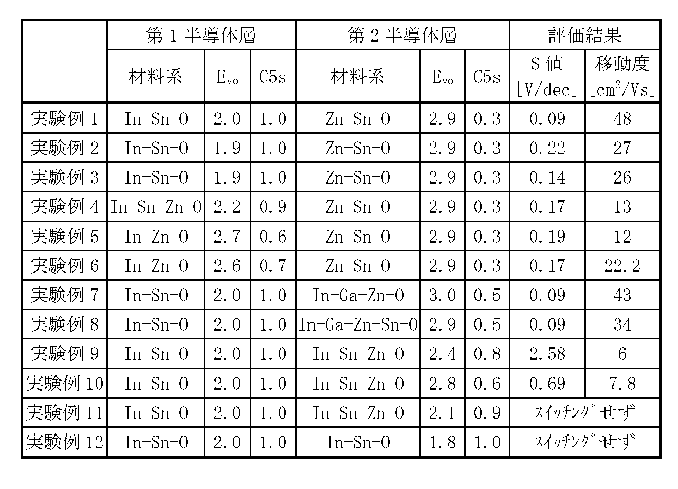
第1半導体層23AのC5sの値が第2半導体層23BのC5sの値よりも大きく、且つ、第2半導体層23BのEVOの値が第1半導体層23AのEVOの値よりも大きな実験例1~実験例10では、デバイスとしての動作を確認することができた。但し、同様の大小関係を有する実験例11では、スイッチングしなかったことから、第2半導体層23BのEVOの値は、2.1eVよりも大きいことが好ましく、2.4eV以上であればデバイスとして動作し、2.8eV以上することで良好に動作することがわかった。第1半導体層23AのC5sの値は、0.6(60)%以上であれば、十分な移動度が得られることがわかった。
The value of C5s the first semiconductor layer 23A is larger than the value of C5s the second semiconductor layer 23B, and the value of E VO of the second semiconductor layer 23B is larger experiment than the value of E VO of the first semiconductor layer 23A In Example 1 to Experimental Example 10, the operation as a device could be confirmed. However, in Examples 11 having the same magnitude relation, since it was not switched, the value of E VO of the second semiconductor layer 23B is preferably larger than 2.1 eV, if more than 2.4eV device It was found that it works well when it is 2.8 eV or more. It was found that if the value of C5s of the first semiconductor layer 23A is 0.6 (60)% or more, sufficient mobility can be obtained.
以上により、本実施の形態の撮像素子10では、第2半導体層23BのC5sの値よりも大きなC5sの値を有する第1半導体層23Aおよび第1半導体層23AのEVOまたはEVNの値よりも大きなEVOまたはEVNの値を有する第2半導体層23Bが下部電極21側からこの順に積層された半導体層23を設けるようにした。これにより、絶縁層22との界面に含まれるトラップが減少し、蓄積電極21Bの上方の半導体層23内に蓄積された電荷の、面内方向への輸送特性が改善される。また、第1半導体層23Aからの酸素または窒素の脱離が低減されるようになり、半導体層23と光電変換層24との間の界面におけるトラップの発生が低減される。よって、残像特性を改善することが可能となる。
Thus, the imaging device 10 of the present embodiment, than the value of E VO or E VN of the first semiconductor layer 23A and the first semiconductor layer 23A has a value of greater C5s than the value of C5s the second semiconductor layer 23B The semiconductor layer 23 in which the second semiconductor layer 23B having a large EVO or EVN value is laminated in this order from the lower electrode 21 side is provided. As a result, the number of traps contained at the interface with the insulating layer 22 is reduced, and the in-plane transport characteristic of the electric charge accumulated in the semiconductor layer 23 above the storage electrode 21B is improved. Further, the desorption of oxygen or nitrogen from the first semiconductor layer 23A is reduced, and the occurrence of traps at the interface between the semiconductor layer 23 and the photoelectric conversion layer 24 is reduced. Therefore, it is possible to improve the afterimage characteristics.
また、例えばIn2O3(ITO)を用いて第1半導体層23Aを形成する場合、成膜方法によっては結晶化することがある。第1半導体層23AがIn2O3(ITO)の結晶層として形成されると、結晶粒界や絶縁層22との界面で欠陥準位が発生し、電気特性が低下する虞がある。これに対して、本実施の形態の撮像素子10では、第1半導体層23Aを非晶質層として形成することにより、第1半導体層23Aのキャリア密度の上昇を防ぎ、低キャリア濃度を実現することができる。また、第1半導体層23Aを結晶層として形成する場合と比較して、第1半導体層23A内の結晶粒界や絶縁層22との界面でのダングリングボンドの発生を抑制し、より低トラップ化することができる。よって、残像特性をさらに改善することが可能となる。
Further, when the first semiconductor layer 23A is formed by using, for example, In 2 O 3 (ITO), it may be crystallized depending on the film forming method. When the first semiconductor layer 23A is formed as a crystal layer of In 2 O 3 (ITO), defect levels may occur at the grain boundaries and the interface with the insulating layer 22, and the electrical characteristics may deteriorate. On the other hand, in the image pickup device 10 of the present embodiment, by forming the first semiconductor layer 23A as an amorphous layer, it is possible to prevent an increase in the carrier density of the first semiconductor layer 23A and realize a low carrier concentration. be able to. Further, as compared with the case where the first semiconductor layer 23A is formed as a crystal layer, the generation of dangling bonds at the grain boundaries in the first semiconductor layer 23A and the interface with the insulating layer 22 is suppressed, and the trap is lower. Can be transformed into. Therefore, it is possible to further improve the afterimage characteristics.
更に、本実施の形態の撮像素子10では、第1半導体層23Aの厚み(t1)に対して、第2半導体層23Bの厚み(t2)の比(t2/t1)が4以上8以下とすることより、第1半導体層23Aから発生したキャリアを第2半導体層23Bで十分に吸収することができる。加えて、第1半導体層23Aを非晶質層とすることにより、半導体層23のキャリア密度の上昇を防ぎつつ、低キャリア濃度を実現することができる。よって、残像特性をさらに改善することが可能となる。
Further, in the image sensor 10 of the present embodiment, the ratio (t2 / t1) of the thickness (t2) of the second semiconductor layer 23B to the thickness (t1) of the first semiconductor layer 23A is 4 or more and 8 or less. Therefore, the carriers generated from the first semiconductor layer 23A can be sufficiently absorbed by the second semiconductor layer 23B. In addition, by forming the first semiconductor layer 23A as an amorphous layer, it is possible to realize a low carrier concentration while preventing an increase in the carrier density of the semiconductor layer 23. Therefore, it is possible to further improve the afterimage characteristics.
次に、本開示の第2の実施の形態および変形例(変形例1~8)について説明する。以下では、上記第1の実施の形態と同様の構成要素については同一の符号を付し、適宜その説明を省略する。
Next, the second embodiment and modified examples (modified examples 1 to 8) of the present disclosure will be described. In the following, the same components as those in the first embodiment will be designated by the same reference numerals, and the description thereof will be omitted as appropriate.
<2.変形例>
(2-1.変形例1)
図20は、本開示の変形例1としての撮像素子の要部(有機光電変換部20A)の断面構成を模式的に表したものである。本変形例の有機光電変換部20Aは、半導体層23と光電変換層24との間に保護層29を設けた点が上記実施の形態とは異なる。 <2. Modification example>
(2-1. Modification 1)
FIG. 20 schematically shows a cross-sectional configuration of a main part (organicphotoelectric conversion part 20A) of an image pickup device as a modification 1 of the present disclosure. The organic photoelectric conversion unit 20A of this modification is different from the above embodiment in that a protective layer 29 is provided between the semiconductor layer 23 and the photoelectric conversion layer 24.
(2-1.変形例1)
図20は、本開示の変形例1としての撮像素子の要部(有機光電変換部20A)の断面構成を模式的に表したものである。本変形例の有機光電変換部20Aは、半導体層23と光電変換層24との間に保護層29を設けた点が上記実施の形態とは異なる。 <2. Modification example>
(2-1. Modification 1)
FIG. 20 schematically shows a cross-sectional configuration of a main part (organic
保護層29は、半導体層23を構成する酸化物半導体材料からの酸素の脱離を防ぐためのものである。保護層29を構成する材料としては、例えば、酸化チタン(TiO2)、ケイ化酸化チタン(TiSiO)、酸化ニオブ(Nb2O5)およびTaOx等が挙げられる。保護層29の厚みは、例えば1原子層あれば効果があり、例えば0.5nm以上10nm以下であることが好ましい。
The protective layer 29 is for preventing the desorption of oxygen from the oxide semiconductor material constituting the semiconductor layer 23. Examples of the material constituting the protective layer 29 include titanium oxide (TIO 2 ), titanium silicate (TiSiO), niobium oxide (Nb 2 O 5 ), TaO x and the like. The thickness of the protective layer 29 is effective if it is, for example, a single atomic layer, and is preferably 0.5 nm or more and 10 nm or less, for example.
このように、本変形例では、半導体層23と光電変換層24との間に保護層29を設けるようにしたので、半導体層23の表面からの酸素または窒素の脱離をさらに低減することが可能となる。これにより、半導体層23(具体的には、第2半導体層23B)と光電変換層24との間の界面におけるトラップの発生がより低減される。また、半導体層23側から光電変換層24への信号電荷(電子)の逆流を防ぐことが可能となる。よって、残像特性および信頼性をさらに向上させることが可能となる。
As described above, in this modification, since the protective layer 29 is provided between the semiconductor layer 23 and the photoelectric conversion layer 24, the desorption of oxygen or nitrogen from the surface of the semiconductor layer 23 can be further reduced. It will be possible. As a result, the occurrence of traps at the interface between the semiconductor layer 23 (specifically, the second semiconductor layer 23B) and the photoelectric conversion layer 24 is further reduced. Further, it is possible to prevent the backflow of signal charges (electrons) from the semiconductor layer 23 side to the photoelectric conversion layer 24. Therefore, it is possible to further improve the afterimage characteristics and reliability.
(2-2.変形例2)
図21は、本開示の変形例2としての撮像素子の要部(有機光電変換部20B)の断面構成の一例を模式的に表したものである。本変形例の有機光電変換部20Bは、下部電極21上に形成された絶縁層22と第1半導体層23Aとの間に、さらに第3半導体層23Cを設けたものである。即ち、本変形例の有機光電変換部20Bは、下部電極21と光電変換層24との間の半導体層23を、下部電極21側から、第3半導体層23C、第1半導体層23Aおよび第2半導体層23Bがこの順に積層された3層構造とした点が上記第1の実施の形態とは異なる。 (2-2. Modification 2)
FIG. 21 schematically shows an example of the cross-sectional configuration of the main part (organicphotoelectric conversion part 20B) of the image pickup device as the second modification of the present disclosure. The organic photoelectric conversion unit 20B of this modification is provided with a third semiconductor layer 23C between the insulating layer 22 formed on the lower electrode 21 and the first semiconductor layer 23A. That is, the organic photoelectric conversion unit 20B of the present modification sets the semiconductor layer 23 between the lower electrode 21 and the photoelectric conversion layer 24 from the lower electrode 21 side to the third semiconductor layer 23C, the first semiconductor layer 23A, and the second semiconductor layer 23A. It differs from the first embodiment in that the semiconductor layer 23B has a three-layer structure in which the semiconductor layers 23B are laminated in this order.
図21は、本開示の変形例2としての撮像素子の要部(有機光電変換部20B)の断面構成の一例を模式的に表したものである。本変形例の有機光電変換部20Bは、下部電極21上に形成された絶縁層22と第1半導体層23Aとの間に、さらに第3半導体層23Cを設けたものである。即ち、本変形例の有機光電変換部20Bは、下部電極21と光電変換層24との間の半導体層23を、下部電極21側から、第3半導体層23C、第1半導体層23Aおよび第2半導体層23Bがこの順に積層された3層構造とした点が上記第1の実施の形態とは異なる。 (2-2. Modification 2)
FIG. 21 schematically shows an example of the cross-sectional configuration of the main part (organic
第3半導体層23Cは、絶縁層22の表面近傍に形成されるダングリングボンドに起因するトラップ準位によって、絶縁層22との界面近傍において半導体層23に蓄積された電荷がトラップされるのを防ぐためのものである。第3半導体層23Cは、絶縁層22の開口22H内に開口23Hを有しており、読み出し電極21Aと第1半導体層23Aとは、開口22H,23Hを介して電気的に接続されている。第3半導体層23Cは、第1半導体層23Aの伝導帯の底(CBM)よりも浅いCBMを有していることが好ましい。これにより、絶縁層22と第3半導体層23Cとの界面近傍に電子が蓄積されるのを防ぐことが可能となる。第3半導体層23Cの構成材料としては、例えば、ZTOやIGZO等を用いることができる。第3半導体層23Cは、第1半導体層23Aおよび第2半導体層23Bと同様に、例えば、スパッタリング法を用いて形成することができる。この他、例えばALD法を用いて形成するようにしてもよい。
In the third semiconductor layer 23C, the charge accumulated in the semiconductor layer 23 is trapped in the vicinity of the interface with the insulating layer 22 by the trap level caused by the dangling bond formed near the surface of the insulating layer 22. It is for prevention. The third semiconductor layer 23C has an opening 23H in the opening 22H of the insulating layer 22, and the readout electrode 21A and the first semiconductor layer 23A are electrically connected to each other via the openings 22H and 23H. The third semiconductor layer 23C preferably has a CBM shallower than the bottom (CBM) of the conduction band of the first semiconductor layer 23A. This makes it possible to prevent electrons from accumulating in the vicinity of the interface between the insulating layer 22 and the third semiconductor layer 23C. As the constituent material of the third semiconductor layer 23C, for example, ZTO, IGZO, or the like can be used. The third semiconductor layer 23C can be formed, for example, by using a sputtering method, similarly to the first semiconductor layer 23A and the second semiconductor layer 23B. In addition, for example, it may be formed by using the ALD method.
このように、本変形例では、下部電極21と第1半導体層23Aとの間に第3半導体層23Cを設けるようにした。これにより、上記第1の実施の形態の効果に加えて、絶縁層22との界面近傍に電子が蓄積されることによる、絶縁層22との界面近傍において電子がトラップされるのを防ぐことが可能となる。即ち、残像特性の悪化を防ぐことが可能となるという効果を奏する。
As described above, in this modification, the third semiconductor layer 23C is provided between the lower electrode 21 and the first semiconductor layer 23A. As a result, in addition to the effect of the first embodiment, it is possible to prevent electrons from being trapped in the vicinity of the interface with the insulating layer 22 due to the accumulation of electrons in the vicinity of the interface with the insulating layer 22. It will be possible. That is, it has the effect of preventing deterioration of the afterimage characteristics.
なお、本変形例の構成は、上記変形例1と組み合わせてもよい。例えば、図22に示した有機光電変換部20Cのように、半導体層23を、第3半導体層23C、第1半導体層23Aおよび第2半導体層23Bがこの順に積層された3層構造とし、さらに、第2半導体層23B上に保護層29を設けるようにしてもよい。これにより、さらに、撮像画質および信頼性を向上させることが可能となる。
The configuration of this modification may be combined with the above modification 1. For example, as in the organic photoelectric conversion unit 20C shown in FIG. 22, the semiconductor layer 23 has a three-layer structure in which the third semiconductor layer 23C, the first semiconductor layer 23A, and the second semiconductor layer 23B are laminated in this order. , The protective layer 29 may be provided on the second semiconductor layer 23B. This makes it possible to further improve the image quality and reliability of the image.
(2-3.変形例3)
図23は、本開示の変形例3としての撮像素子の要部(有機光電変換部20D)の断面構成を模式的に表したものである。本変形例の有機光電変換部20Dは、読み出し電極21Aと蓄積電極21Bとの間に転送電極21Cを設けた点が上記実施の形態とは異なる。 (2-3. Modification 3)
FIG. 23 schematically shows the cross-sectional configuration of the main part (organicphotoelectric conversion part 20D) of the image pickup device as the third modification of the present disclosure. The organic photoelectric conversion unit 20D of this modification is different from the above embodiment in that the transfer electrode 21C is provided between the readout electrode 21A and the storage electrode 21B.
図23は、本開示の変形例3としての撮像素子の要部(有機光電変換部20D)の断面構成を模式的に表したものである。本変形例の有機光電変換部20Dは、読み出し電極21Aと蓄積電極21Bとの間に転送電極21Cを設けた点が上記実施の形態とは異なる。 (2-3. Modification 3)
FIG. 23 schematically shows the cross-sectional configuration of the main part (organic
転送電極21Cは、蓄積電極21Bの上方に蓄積された電荷の読み出し電極21Aへの転送効率を向上させるためのものであり、読み出し電極21Aと蓄積電極21Bとの間に設けられている。具体的には、転送電極21Cは、例えば、読み出し電極21Aおよび蓄積電極21Bが設けられた層よりも下層に形成され、一部が読み出し電極21Aおよび蓄積電極21Bと重複するように設けられている。
The transfer electrode 21C is for improving the transfer efficiency of the electric charge accumulated above the storage electrode 21B to the read-out electrode 21A, and is provided between the read-out electrode 21A and the storage electrode 21B. Specifically, the transfer electrode 21C is formed, for example, in a layer lower than the layer provided with the read-out electrode 21A and the storage electrode 21B, and is partially provided so as to overlap the read-out electrode 21A and the storage electrode 21B. ..
読み出し電極21A、蓄積電極21Bおよび転送電極21Cは、各々独立して電圧を印加できるようになっている。本変形例では、リセット動作の完了後の転送期間に、駆動回路から読み出し電極21Aに電位V5、蓄積電極21Bに電位V6、転送電極21Cに電位V7(V5>V6>V7)が印加される。これにより、蓄積電極21Bの上方に蓄積されていた電荷は、蓄積電極21B上から転送電極21C上および読み出し電極21A上の順に移動し、フローティングディフュージョンFD1へと読み出される。
A voltage can be applied independently to the read electrode 21A, the storage electrode 21B, and the transfer electrode 21C. In this modification, the potential V5 is applied to the reading electrode 21A, the potential V6 is applied to the storage electrode 21B, and the potential V7 (V5> V6> V7) is applied to the transfer electrode 21C during the transfer period after the completion of the reset operation. As a result, the electric charge accumulated above the storage electrode 21B moves from the storage electrode 21B to the transfer electrode 21C and the read-out electrode 21A in this order, and is read out to the floating diffusion FD1.
このように本変形例では、読み出し電極21Aと蓄積電極21Bとの間に、転送電極21Cを設けるようにした。これにより、より確実に読み出し電極21AからフローティングディフュージョンFD1へ電荷を移動させることが可能となり、読み出し電極21Aへの電荷の輸送特性がさらに改善され、ノイズを低減することが可能となる。
As described above, in this modification, the transfer electrode 21C is provided between the read electrode 21A and the storage electrode 21B. As a result, the charge can be more reliably transferred from the read-out electrode 21A to the floating diffusion FD1, the charge transport characteristic to the read-out electrode 21A is further improved, and noise can be reduced.
<3.第2の実施の形態>
図24は、本開示の第2の実施の形態に係る撮像素子(撮像素子10A)の断面構成を表したものである。図25は、図24に示した撮像素子10Aの要部(有機光電変換部80)の断面構成の一例を拡大して模式的に表したものである。撮像素子10Aは、例えば、デジタルスチルカメラ、ビデオカメラ等の電子機器に用いられるCMOSイメージセンサ等の撮像装置(例えば、撮像装置1)の画素部1Aにおいてアレイ状に繰り返し配置される1つの画素(単位画素P)を構成するものである。 <3. Second Embodiment>
FIG. 24 shows the cross-sectional configuration of the image pickup device (image pickup device 10A) according to the second embodiment of the present disclosure. FIG. 25 is an enlarged schematic representation of an example of the cross-sectional configuration of the main part (organic photoelectric conversion unit 80) of the image sensor 10A shown in FIG. 24. The image sensor 10A is, for example, one pixel (for example) that is repeatedly arranged in an array in the pixel unit 1A of an image pickup device (for example, an image pickup device 1) such as a CMOS image sensor used in an electronic device such as a digital still camera or a video camera. It constitutes a unit pixel P).
図24は、本開示の第2の実施の形態に係る撮像素子(撮像素子10A)の断面構成を表したものである。図25は、図24に示した撮像素子10Aの要部(有機光電変換部80)の断面構成の一例を拡大して模式的に表したものである。撮像素子10Aは、例えば、デジタルスチルカメラ、ビデオカメラ等の電子機器に用いられるCMOSイメージセンサ等の撮像装置(例えば、撮像装置1)の画素部1Aにおいてアレイ状に繰り返し配置される1つの画素(単位画素P)を構成するものである。 <3. Second Embodiment>
FIG. 24 shows the cross-sectional configuration of the image pickup device (
本実施の形態の撮像素子10Aでは、有機光電変換部80は、対向配置された、読み出し電極21Aおよび蓄積電極21Bからなる下部電極21と上部電極25との間に、半導体層83および光電変換層84が、下部電極21側からこの順に積層されている。半導体層83は、例えば第1半導体層83Aおよび第2半導体層83Bからなり、下部電極21側からこの順に積層されている。第1半導体層83Aは、第2半導体層83BのΔENの値よりも小さなΔENの値を有しており、第2半導体層83Bは、上記第1の実施の形態と同様に、第1半導体層83AのEVOの値よりも大きなEVOの値を有している。
In the image pickup device 10A of the present embodiment, the organic photoelectric conversion unit 80 has a semiconductor layer 83 and a photoelectric conversion layer between the lower electrode 21 and the upper electrode 25, which are arranged so as to face each other and consist of a readout electrode 21A and a storage electrode 21B. 84 are laminated in this order from the lower electrode 21 side. The semiconductor layer 83 is composed of, for example, a first semiconductor layer 83A and a second semiconductor layer 83B, and is laminated in this order from the lower electrode 21 side. The first semiconductor layer 83A has a value of ΔEN smaller than the value of ΔEN of the second semiconductor layer 83B, and the second semiconductor layer 83B is the first semiconductor layer as in the first embodiment. It has a value of greater E VO than the value of E VO of 83A.
半導体層83は、光電変換層84で発生した電荷を蓄積するためのものである。半導体層83は、上記のように、第1半導体層83Aと第2半導体層83Bとが下部電極21側からこの順に積層された積層構造を有している。具体的には、第1半導体層83Aは、下部電極21と半導体層83とを電気的に分離する絶縁層22上に設けられ、読み出し電極21A上に設けられた開口22H内において、読み出し電極21Aと直接電気的に接続されている。第2半導体層83Bは、第1半導体層83Aと光電変換層84との間に設けられている。
The semiconductor layer 83 is for accumulating the electric charge generated in the photoelectric conversion layer 84. As described above, the semiconductor layer 83 has a laminated structure in which the first semiconductor layer 83A and the second semiconductor layer 83B are laminated in this order from the lower electrode 21 side. Specifically, the first semiconductor layer 83A is provided on the insulating layer 22 that electrically separates the lower electrode 21 and the semiconductor layer 83, and the read electrode 21A is provided in the opening 22H provided on the read electrode 21A. Is directly electrically connected to. The second semiconductor layer 83B is provided between the first semiconductor layer 83A and the photoelectric conversion layer 84.
第1半導体層83Aは、第2半導体層83BのΔENの値よりも小さなΔENの値を有する酸化物半導体材料を含んで形成することができる。第2半導体層83Bは、上記第1の実施の形態と同様に、第1半導体層83AのEVOの値よりも大きなEVOの値を有する酸化物半導体材料を含んで形成することができる。
The first semiconductor layer 83A can be formed by including an oxide semiconductor material having a ΔEN value smaller than the ΔEN value of the second semiconductor layer 83B. The second semiconductor layer 83B can be formed by including an oxide semiconductor material having an EVO value larger than the EVO value of the first semiconductor layer 83A, as in the first embodiment.
ΔENは、酸化物半導体がイオン性か共有結合性かを判断する指標であり、酸化物半導体中で、電無機半導体材料層を構成するアニオン種の電気陰性度の平均値ENanionから、無機半導体材料層を構成するカチオン種の電気陰性度の平均値ENcationを減じた値(ΔEN=ENanion-ENcation)として定義される。イオン性が高い(ΔENが大きい)場合、酸化物半導体中の静電ポテンシャルの起伏が激しく、共有結合性が高い(ΔENが小さい)場合、静電ポテンシャルの起伏が緩やかになる。酸化物半導体では、共有結合性が高い方が、酸化物半導体中の水素原子(プロトンまたはヒドリドイオン)がより低温でも拡散しやすく、低温のアニール条件でも良質な膜を形成することができる。なお、ここでいう平均は、各種金属元素の電気陰性度を、その酸化物半導体中の組成(原子%)で平均した値である。
ΔEN is an index for determining whether the oxide semiconductor is ionic or covalent, and is an inorganic semiconductor material based on the average electronegativity ENanion of the anion species constituting the electro-inorganic semiconductor material layer in the oxide semiconductor. It is defined as a value obtained by subtracting the average electronegativity of the electronegativity of the cation species constituting the layer, Encation (ΔEN = ENanion-Encation). When the ionicity is high (ΔEN is large), the undulations of the electrostatic potential in the oxide semiconductor are severe, and when the covalent bond is high (ΔEN is small), the undulations of the electrostatic potential are gentle. In an oxide semiconductor, the higher the covalent bond, the easier it is for hydrogen atoms (protons or hydride ions) in the oxide semiconductor to diffuse even at a lower temperature, and a good quality film can be formed even under low temperature annealing conditions. The average here is a value obtained by averaging the electronegativity of various metal elements with the composition (atomic%) in the oxide semiconductor.
第1半導体層83Aは、例えば、In、Sn、Zn、Ga、Ti、AlおよびW等のうちの2種以上の元素を含む酸化物半導体材料を用いることで形成することができる。また、第2半導体層83Bは、例えば、Ga、Al、Ti、Zn、Sn、InおよびW等のうちの2種以上の元素を含む酸化物半導体材料を用いることで形成することができる。
The first semiconductor layer 83A can be formed by using, for example, an oxide semiconductor material containing two or more kinds of elements such as In, Sn, Zn, Ga, Ti, Al and W. Further, the second semiconductor layer 83B can be formed by using, for example, an oxide semiconductor material containing two or more kinds of elements such as Ga, Al, Ti, Zn, Sn, In and W.
より具体的には、例えば、第1半導体層83Aを構成する酸化物半導体材料の組成をAaBbOcで表した場合、Aの元素は、In、Sn、Zn、Ga、Ti、AlおよびWのいずれかであり、Bの元素は、In、Sn、Zn、Ga、Ti、AlおよびWのうちAで選択した元素以外の元素のいずれかであり、その組成比はa>bまたはb>aを満たすことが好ましい。また、a,bは、a+b+c=1.00においてa>bまたはb>aを満たすことが好ましい。第1半導体層83Aを構成する酸化物半導体材料の組成をAaBbCcOdで表した場合、Aの元素は、In、Sn、Zn、Ga、Ti、AlおよびWのいずれかであり、Bの元素は、In、Sn、Zn、Ga、Ti、AlおよびWのうちAで選択した元素以外の元素のいずれかであり、Cの元素は、In、Sn、Zn、Ga、Ti、AlおよびWのうちAおよびBで選択した元素以外の元素のいずれかであり、その組成比は、aが最も比率が高く、c>bまたはb>cを満たすことが好ましく、より好ましくはc>bである。また、a,b,cは、a+b+c+d=1.00においてa>b+cを満たすことが好ましい。
More specifically, for example, when the composition of the oxide semiconductor material constituting the first semiconductor layer 83A is represented by AaBbOc, the element of A is any one of In, Sn, Zn, Ga, Ti, Al and W. The element B is any of In, Sn, Zn, Ga, Ti, Al and W other than the element selected in A, and the composition ratio satisfies a> b or b> a. Is preferable. Further, a and b preferably satisfy a> b or b> a at a + b + c = 1.00. When the composition of the oxide semiconductor material constituting the first semiconductor layer 83A is represented by AaBbCcOd, the element of A is any of In, Sn, Zn, Ga, Ti, Al and W, and the element of B is It is any of the elements other than the element selected in A among In, Sn, Zn, Ga, Ti, Al and W, and the element C is A among In, Sn, Zn, Ga, Ti, Al and W. And any of the elements other than the element selected in B, and the composition ratio thereof is preferably that a has the highest ratio and satisfies c> b or b> c, and more preferably c> b. Further, a, b, and c preferably satisfy a> b + c at a + b + c + d = 1.00.
第2半導体層83Bでは、第2半導体層83Bを構成する酸化物半導体材料の組成をAaBbOcで表した場合、Aの元素は、Ga、Al、Ti、Zn、Sn、InおよびWのいずれかであり、Bの元素は、Ga、Al、Ti、Zn、Sn、InおよびWのうちAで選択した元素以外の元素のいずれかであり、その組成比は、a>bまたはb>aを満たすことが好ましい。また、a,bは、a+b+c=1.00においてa>bまたはb>aを満たすことが好ましい。第2半導体層83Bを構成する酸化物半導体材料の組成をAaBbCcOdで表した場合、Aの元素は、Ga、Al、Ti、Zn、Sn、InおよびWのいずれかであり、Bの元素は、Ga、Al、Ti、Zn、Sn、InおよびWのうちAで選択した元素以外の元素のいずれかであり、Cの元素は、In、Sn、Zn、Ga、Ti、AlおよびWのうちAおよびBで選択した元素以外の元素のいずれかであり、その組成比は、aが最も比率が高く、c>bまたはb>cを満たすことが好ましく、より好ましくはc>bである。また、a,b,cは、a+b+c+d=1.00においてa>b+cを満たすことが好ましい。
In the second semiconductor layer 83B, when the composition of the oxide semiconductor material constituting the second semiconductor layer 83B is represented by AaBbOc, the element of A is any of Ga, Al, Ti, Zn, Sn, In and W. Yes, the element B is any of Ga, Al, Ti, Zn, Sn, In and W other than the element selected in A, and the composition ratio satisfies a> b or b> a. Is preferable. Further, a and b preferably satisfy a> b or b> a at a + b + c = 1.00. When the composition of the oxide semiconductor material constituting the second semiconductor layer 83B is represented by AaBbCcOd, the element of A is any of Ga, Al, Ti, Zn, Sn, In and W, and the element of B is It is any of the elements other than the element selected in A among Ga, Al, Ti, Zn, Sn, In and W, and the element C is A among In, Sn, Zn, Ga, Ti, Al and W. And any of the elements other than the element selected in B, and the composition ratio thereof is preferably that a has the highest ratio and satisfies c> b or b> c, and more preferably c> b. Further, a, b, and c preferably satisfy a> b + c at a + b + c + d = 1.00.
なお、光電変換層84との界面を形成する第2半導体層83Bの表面粗さRaは、1.5nm以下であることが好ましい。また、光電変換層84との界面を形成する第2半導体層83Bの二乗平均平方根粗さRqは、2.5nm以下であることが好ましい。これにより、上述した保護層29や光電変換層84を含むその他の有機層を形成することが可能となる。更に、第2半導体層83Bのキャリア濃度は、1×10¹⁴/cm-3以上1×1017/cm-3未満であることが好ましい。これにより、半導体層83を空乏化することが可能となる。
The surface roughness Ra of the second semiconductor layer 83B forming the interface with the photoelectric conversion layer 84 is preferably 1.5 nm or less. Further, the root mean square roughness Rq of the second semiconductor layer 83B forming the interface with the photoelectric conversion layer 84 is preferably 2.5 nm or less. This makes it possible to form other organic layers including the protective layer 29 and the photoelectric conversion layer 84 described above. Further, the carrier concentration of the second semiconductor layer 83B is preferably 1 × 10 14 / cm -3 or more and less than 1 × 10 17 / cm -3. This makes it possible to deplete the semiconductor layer 83.
半導体層83は、10cm2/V・s以上のキャリア移動度を有していることが好ましい。半導体層83は、例えば非晶質構造を有し、その厚みは、例えば、10nm以上150nm以下である。
The semiconductor layer 83 preferably has a carrier mobility of 10 cm 2 / V · s or more. The semiconductor layer 83 has, for example, an amorphous structure, and the thickness thereof is, for example, 10 nm or more and 150 nm or less.
なお、第1半導体層83Aおよび第2半導体層83Bには、その成膜過程において水素(H)や他の金属元素等の不純物が混入する場合があるが、微量(例えばモル分率で3%以下)であれば混入を妨げるものではない。
Impurities such as hydrogen (H) and other metal elements may be mixed in the first semiconductor layer 83A and the second semiconductor layer 83B in the film forming process, but in a trace amount (for example, 3% in terms of mole fraction). If it is (below), it does not prevent mixing.
また、第1半導体層83Aおよび第2半導体層83Bの構成材料としては、上記第1の実施の形態と同様に、窒化物半導体材料や酸窒化物半導体材料も用いることができる。窒化物半導体材料を用いて第1半導体層83Aおよび第2半導体層83Bを形成する場合には、酸素欠損生成エネルギーEVOに代えて、窒素欠損生成エネルギーEVNを指標として用いる。その場合においても、第1半導体層83Aは、第2半導体層83BのΔENの値よりも小さなΔENの値を有しており、第2半導体層83Bは、第1半導体層83AのEVNの値よりも大きなEVNの値を有しており、第2半導体層83Bは、第1半導体層83AのEVNの値よりも大きなEVNの値を有する窒化物半導体材料を含んで形成することができる。
Further, as the constituent material of the first semiconductor layer 83A and the second semiconductor layer 83B, a nitride semiconductor material or an oxynitride semiconductor material can also be used as in the first embodiment. When the first semiconductor layer 83A and the second semiconductor layer 83B are formed by using the nitride semiconductor material, the nitrogen deficiency generation energy EVN is used as an index instead of the oxygen deficiency generation energy EVO. Also in this case, the first semiconductor layer 83A has a value smaller ΔEN than the value of ΔEN the second semiconductor layer 83B, the second semiconductor layer 83B, the value of E VN of the first semiconductor layer 83A It has a value of greater E VN than, the second semiconductor layer 83B may be than the value of E VN of the first semiconductor layer 83A is formed to include a nitride semiconductor material having a large value of E VN can.
光電変換層84は、光エネルギーを電気エネルギーに変換するためのものである。光電変換層84は、上記第1の実施の形態における光電変換層24と同様の構成としてもよいが、本実施の形態では、半導体層83近傍に位置する材料のLowest Unoccupied Molecular Orbital(LUMO)準位E1と、半導体層83を構成する酸化物半導体材料のLUMO準位E2とが、E2-E1≧0.1eVを満たしていることが好ましく、より好ましくは、E2-E1>0.1eVである。これにより、光電変換層84で発生した電子を半導体層83に移動させることが可能となる。
The photoelectric conversion layer 84 is for converting light energy into electrical energy. The photoelectric conversion layer 84 may have the same configuration as the photoelectric conversion layer 24 in the first embodiment, but in the present embodiment, the material located in the vicinity of the semiconductor layer 83 is the lowest unoccupied molecular orbital (LUMO) quasi. The position E1 and the LUMO level E2 of the oxide semiconductor material constituting the semiconductor layer 83 preferably satisfy E2-E1 ≧ 0.1 eV, and more preferably E2-E1> 0.1 eV. .. This makes it possible to move the electrons generated in the photoelectric conversion layer 84 to the semiconductor layer 83.
なお、半導体層83および光電変換層84のエネルギー準位は、例えば、スパッタリング法を用いて各層を形成する際に用いる酸素ガスの導入量(酸素ガス分圧)を調整することで制御することができる。また、半導体層83のキャリア移動度および第2半導体層83Bのキャリア濃度については、組成比率を調整することで制御することができる。
The energy levels of the semiconductor layer 83 and the photoelectric conversion layer 84 can be controlled by, for example, adjusting the amount of oxygen gas introduced (oxygen gas partial pressure) used when forming each layer by using a sputtering method. can. Further, the carrier mobility of the semiconductor layer 83 and the carrier concentration of the second semiconductor layer 83B can be controlled by adjusting the composition ratio.
以上、本実施の形態の撮像素子10Aでは、読み出し電極21Aおよび蓄積電極21Bからなる下部電極21と光電変換層84との間に、第2半導体層83BのΔENの値よりも小さなΔENの値を有する第1半導体層83Aおよび第1半導体層83AのEVOの値よりも大きなEVOの値を有する第2半導体層83Bが、下部電極21側からこの順に積層された半導体層83を設けるようにした。これにより、第1半導体層83A内では、水素の拡散が促進されるようになり、電荷のトラップとなる欠陥サイトの発生が低減され、蓄積電極21Bの上方の半導体層83内に蓄積された電荷の、面内方向への輸送特性が改善される。また、半導体層23と光電変換層24との間の界面におけるトラップの発生が低減される。よって、上記第1の実施の形態と同様に、残像特性を改善することが可能となる。
As described above, in the image pickup device 10A of the present embodiment, the value of ΔEN smaller than the value of ΔEN of the second semiconductor layer 83B is set between the lower electrode 21 composed of the readout electrode 21A and the storage electrode 21B and the photoelectric conversion layer 84. The first semiconductor layer 83A and the second semiconductor layer 83B having an EVO value larger than the EVO value of the first semiconductor layer 83A are provided so as to provide the semiconductor layer 83 laminated in this order from the lower electrode 21 side. bottom. As a result, the diffusion of hydrogen is promoted in the first semiconductor layer 83A, the generation of defective sites that become charge traps is reduced, and the charge accumulated in the semiconductor layer 83 above the storage electrode 21B is reduced. The transport characteristics in the in-plane direction are improved. Further, the occurrence of traps at the interface between the semiconductor layer 23 and the photoelectric conversion layer 24 is reduced. Therefore, it is possible to improve the afterimage characteristics as in the first embodiment.
また、一般に、光電変換層84のように有機材料を含む層は耐熱性が低く、高温条件に曝されることにより特性が劣化する虞がある。これに対して、本実施の形態の撮像素子10Aでは、第1半導体層83AのΔENを小さくしたので、一般的な有機光電変換部よりも低温での製造が可能となる。これは、後述する変形例4,5における複数の有機光電変換部が積層された撮像素子10B,10Cにおいて特に有用であり、上層に配置される有機光電変換部(例えば、撮像素子10Bでは、有機光電変換部70)を形成する際に、下層に配置される有機光電変換部の光電変換層(例えば、撮像素子10Bでは、有機光電変換部20の光電変換層24)の特性の劣化を防ぐことができる。よって、デバイス特性の劣化を防ぐことが可能となる。
Further, in general, a layer containing an organic material such as the photoelectric conversion layer 84 has low heat resistance, and there is a risk that the characteristics will deteriorate when exposed to high temperature conditions. On the other hand, in the image sensor 10A of the present embodiment, since ΔEN of the first semiconductor layer 83A is reduced, it is possible to manufacture the image sensor at a lower temperature than that of a general organic photoelectric conversion unit. This is particularly useful in the image pickup devices 10B and 10C in which a plurality of organic photoelectric conversion sections are laminated in the modified examples 4 and 5 described later, and the organic photoelectric conversion section arranged in the upper layer (for example, in the image pickup device 10B is organic). When forming the photoelectric conversion unit 70), it is necessary to prevent deterioration of the characteristics of the photoelectric conversion layer of the organic photoelectric conversion unit (for example, in the image pickup element 10B, the photoelectric conversion layer 24 of the organic photoelectric conversion unit 20) arranged in the lower layer. Can be done. Therefore, it is possible to prevent deterioration of device characteristics.
更に、本実施の形態の撮像素子10Aでは、上記構成とすることにより、半導体層83のLUMO値およびキャリア移動度をバランスよく制御することが可能となる。
Further, in the image pickup device 10A of the present embodiment, the LUMO value and the carrier mobility of the semiconductor layer 83 can be controlled in a well-balanced manner by the above configuration.
表3は、GZTO(Ga-Zn-Sn-O系酸化物半導体)、IGZO(In-Ga-Zn-O系酸化物半導体)またはZnTiSnOを用いて半導体層83(第2半導体層83B)を形成した際の、各組成比におけるキャリア移動度およびキャリア濃度をまとめたものである。また、図26は、実験例13~実験例18におけるGa含有量とキャリア移動度との関係を表したものである。図27は、実験例13~実験例18におけるGaの含有量とキャリア濃度との関係を表したものである。各評価用試料(実験例13~21)は、まず、基板上にITOからなる下部電極21を形成した後、下部電極21上に半導体層83(第2半導体層83B)、光電変換層84、MoOxからなるバッファ層、上部電極25を順次積層した。半導体層83の厚さは100nmとした。
In Table 3, GZTO (Ga-Zn-Sn-O-based oxide semiconductor), IGZO (In-Ga-Zn-O-based oxide semiconductor) or ZnTiSnO is used to form the semiconductor layer 83 (second semiconductor layer 83B). The carrier mobility and carrier concentration at each composition ratio are summarized. Further, FIG. 26 shows the relationship between the Ga content and the carrier mobility in Experimental Examples 13 to 18. FIG. 27 shows the relationship between the Ga content and the carrier concentration in Experimental Examples 13 to 18. In each evaluation sample (Experimental Examples 13 to 21), first, a lower electrode 21 made of ITO is formed on a substrate, and then a semiconductor layer 83 (second semiconductor layer 83B), a photoelectric conversion layer 84, and the like are formed on the lower electrode 21. A buffer layer made of MoO x and an upper electrode 25 were sequentially laminated. The thickness of the semiconductor layer 83 was set to 100 nm.
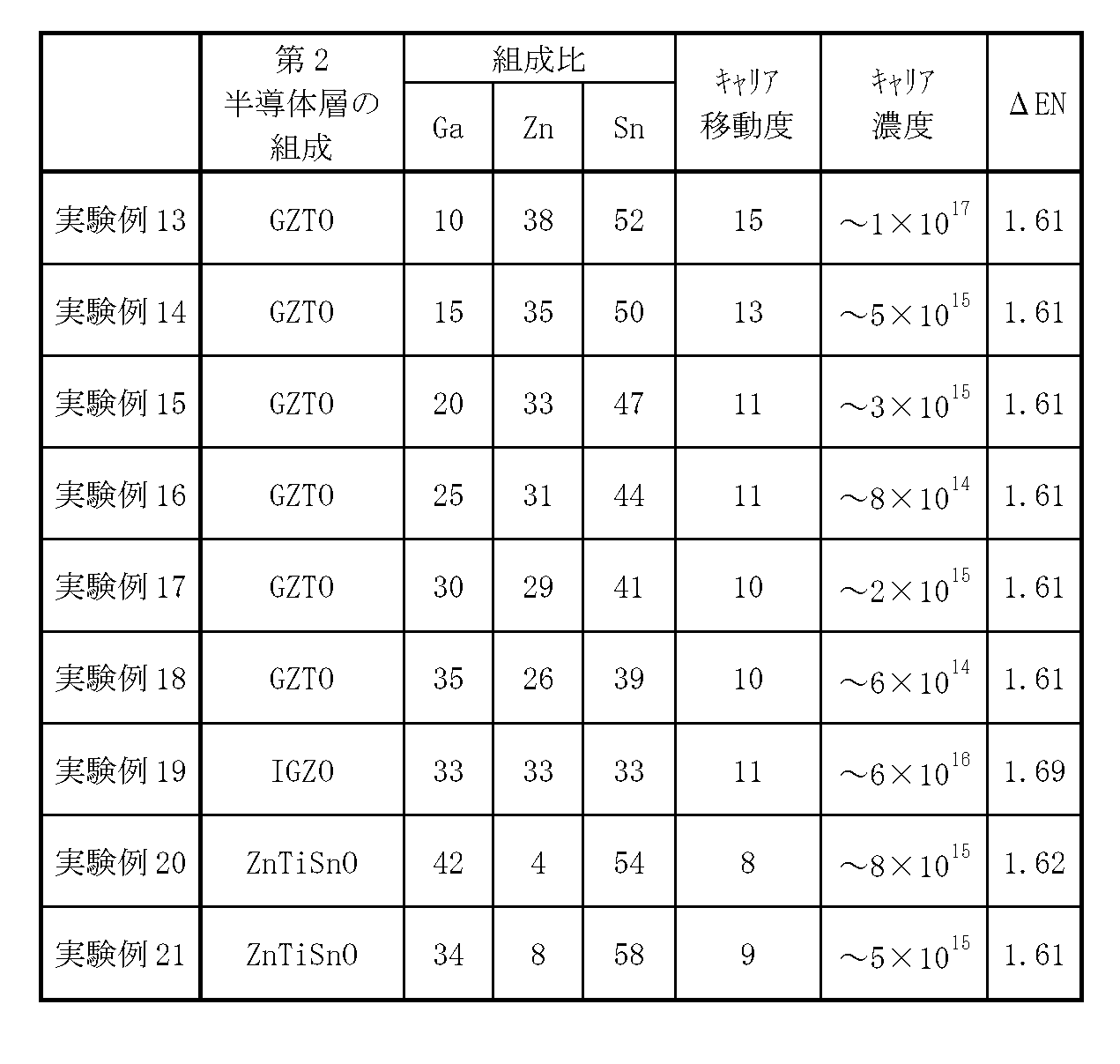
上記実験例13~実験例21は、正バイアスとして2Vを印加したとき、1×10⁻¹⁰/cm2以下の暗電流特性(Jdk)を示し、外部量子効率(EQE)に関しては、正バイアスとして2Vを印加したとき、75%以上の結果が得られた。なお、下部電極と光電変換層との間に半導体層を設けない一般的なデバイスにおいて、同条件で暗電流特性(Jdk)およびEQEを測定した場合、暗電流特性(Jdk)に関しては、実験例13~実験例21と同程度の結果が得られた。また、EQEに関しては、一般的なデバイスでは70%であったことから、本実施の形態の撮像素子10Bでは、良好な暗電流特性(Jdk)を保ちつつ、EQEを向上させることができることがわかる。
Experimental Example 13 to Experiment Example 21, upon application of a 2V as positive bias, 1 × 10 -10 / cm 2 less shows dark current characteristics (J dk), with respect to the external quantum efficiency (EQE) is positively biased When 2V was applied, a result of 75% or more was obtained. Incidentally, in a general device without the semiconductor layer between the lower electrode and the photoelectric conversion layer, when measured dark current characteristics (J dk) and EQE under the same conditions, with respect to the dark current characteristics (J dk) is Results similar to those of Experimental Examples 13 to 21 were obtained. As for the EQE, a typical device from that was 70%, the imaging device 10B of the present embodiment, while maintaining a good dark current property (J dk), that can improve the EQE Recognize.
なお、本実施の形態の撮像素子10Aでは、上記第1の実施の形態と同様に、第1半導体層83Aを非晶質層として形成することにより、第1半導体層83Aのキャリア密度の上昇を防ぎ、低キャリア濃度を実現することができる。また、第1半導体層83Aを結晶層として形成する場合と比較して、第1半導体層83A内の結晶粒界や絶縁層22との界面でのダングリングボンドの発生を抑制し、より低トラップ化することができる。よって、残像特性をさらに改善することが可能となる。
In the image sensor 10A of the present embodiment, the carrier density of the first semiconductor layer 83A is increased by forming the first semiconductor layer 83A as an amorphous layer as in the first embodiment. It can be prevented and a low carrier concentration can be achieved. Further, as compared with the case where the first semiconductor layer 83A is formed as a crystal layer, the generation of dangling bonds at the grain boundaries in the first semiconductor layer 83A and the interface with the insulating layer 22 is suppressed, and the trap is lower. Can be transformed into. Therefore, it is possible to further improve the afterimage characteristics.
また、本実施の形態の撮像素子10Aでは、上記第1の実施の形態と同様に、第1半導体層83Aの厚み(t1)に対して、第2半導体層83Bの厚み(t2)の比(t2/t1)が4以上8以下とすることより、第1半導体層83Aから発生したキャリアを第2半導体層83Bで十分に吸収することができる。加えて、第1半導体層83Aを非晶質層とすることにより、半導体層83のキャリア密度の上昇を防ぎつつ、低キャリア濃度を実現することができる。よって、残像特性をさらに改善することが可能となる。
Further, in the image sensor 10A of the present embodiment, the ratio of the thickness (t2) of the second semiconductor layer 83B to the thickness (t1) of the first semiconductor layer 83A is the same as that of the first embodiment. By setting t2 / t1) to 4 or more and 8 or less, the carriers generated from the first semiconductor layer 83A can be sufficiently absorbed by the second semiconductor layer 83B. In addition, by forming the first semiconductor layer 83A as an amorphous layer, it is possible to realize a low carrier concentration while preventing an increase in the carrier density of the semiconductor layer 83. Therefore, it is possible to further improve the afterimage characteristics.
更に、本技術は、以下のような構成を有する撮像素子にも適用することができる。
Furthermore, this technology can also be applied to an image sensor having the following configuration.
<4.変形例>
(4-1.変形例4)
図28は、本開示の変形例4に係る撮像素子(撮像素子10B)の断面構成を表したものである。撮像素子10Bは、例えば、デジタルスチルカメラ、ビデオカメラ等の電子機器に用いられるCMOSイメージセンサ等の撮像装置(撮像装置1)の画素部1Aにおいてアレイ状に繰り返し配置される1つの画素(単位画素P)を構成するものである。本変形例の撮像素子10Bは、2つの有機光電変換部20および有機光電変換部70と、1つの無機光電変換部32とが縦方向に積層されたものである。 <4. Modification example>
(4-1. Modification 4)
FIG. 28 shows the cross-sectional configuration of the image pickup device (image pickup device 10B) according to the modified example 4 of the present disclosure. The image sensor 10B is, for example, one pixel (unit pixel) repeatedly arranged in an array in the pixel unit 1A of an image pickup device (imaging device 1) such as a CMOS image sensor used in an electronic device such as a digital still camera or a video camera. It constitutes P). The image pickup device 10B of this modification is a stack of two organic photoelectric conversion units 20, an organic photoelectric conversion unit 70, and one inorganic photoelectric conversion unit 32 in the vertical direction.
(4-1.変形例4)
図28は、本開示の変形例4に係る撮像素子(撮像素子10B)の断面構成を表したものである。撮像素子10Bは、例えば、デジタルスチルカメラ、ビデオカメラ等の電子機器に用いられるCMOSイメージセンサ等の撮像装置(撮像装置1)の画素部1Aにおいてアレイ状に繰り返し配置される1つの画素(単位画素P)を構成するものである。本変形例の撮像素子10Bは、2つの有機光電変換部20および有機光電変換部70と、1つの無機光電変換部32とが縦方向に積層されたものである。 <4. Modification example>
(4-1. Modification 4)
FIG. 28 shows the cross-sectional configuration of the image pickup device (
有機光電変換部20,70と、無機光電変換部32とは、互いに異なる波長域の光を選択的に検出して光電変換を行うものである。例えば、有機光電変換部20では緑(G)の色信号を取得する。例えば、有機光電変換部70は青(B)の色信号を取得する。例えば、無機光電変換部32では赤(R)の色信号を取得する。これにより、撮像素子10Bでは、カラーフィルタを用いることなく一つの単位画素Pにおいて複数種類の色信号を取得可能となっている。
The organic photoelectric conversion units 20 and 70 and the inorganic photoelectric conversion unit 32 selectively detect light in different wavelength ranges and perform photoelectric conversion. For example, the organic photoelectric conversion unit 20 acquires a green (G) color signal. For example, the organic photoelectric conversion unit 70 acquires a blue (B) color signal. For example, the inorganic photoelectric conversion unit 32 acquires a red (R) color signal. As a result, the image sensor 10B can acquire a plurality of types of color signals in one unit pixel P without using a color filter.
有機光電変換部70は、例えば有機光電変換部20の上方に積層され、有機光電変換部20と同様に、下部電極71、例えば第1半導体層73Aおよび第2半導体層73Bを含む半導体層73、光電変換層74、および上部電極75が、半導体基板30の第1面30Aの側からこの順に積層された構成を有している。また、下部電極71と半導体層73との間には、絶縁層72が設けられている。下部電極71は、例えば、撮像素子10Bごとに分離形成されると共に、絶縁層72を間に互いに分離された読み出し電極71Aおよび蓄積電極71Bによって構成されている。下部電極71のうち、読み出し電極71Aは、絶縁層72に設けられた開口72Hを介して第1半導体層72Aと電気的に接続されている。半導体層73、光電変換層74および上部電極75は、図28では、撮像素子10Bごとに分離形成されている例を示したが、例えば、複数の撮像素子10Bに共通した連続層として設けられていてもよい。
The organic photoelectric conversion unit 70 is laminated on the organic photoelectric conversion unit 20, for example, and similarly to the organic photoelectric conversion unit 20, the lower electrode 71, for example, the semiconductor layer 73 including the first semiconductor layer 73A and the second semiconductor layer 73B, The photoelectric conversion layer 74 and the upper electrode 75 are laminated in this order from the side of the first surface 30A of the semiconductor substrate 30. Further, an insulating layer 72 is provided between the lower electrode 71 and the semiconductor layer 73. The lower electrode 71 is composed of, for example, a readout electrode 71A and a storage electrode 71B which are separated and formed for each image sensor 10B and whose insulating layer 72 is separated from each other. Of the lower electrodes 71, the readout electrode 71A is electrically connected to the first semiconductor layer 72A via an opening 72H provided in the insulating layer 72. In FIG. 28, the semiconductor layer 73, the photoelectric conversion layer 74, and the upper electrode 75 are separately formed for each image sensor 10B. For example, the semiconductor layer 73, the photoelectric conversion layer 74, and the upper electrode 75 are provided as a continuous layer common to a plurality of image sensors 10B. You may.
半導体層73は、光電変換層74で発生した電荷を蓄積するためのものである。半導体層73は、半導体層23と同様に、第1半導体層73Aと第2半導体層73Bとが下部電極71側からこの順に積層された積層構造を有している。具体的には、第1半導体層73Aは、下部電極71と半導体層73とを電気的に分離する絶縁層72上に設けられ、読み出し電極71A上に設けられた開口72H内において読み出し電極71Aと電気的に接続されている。第2半導体層73Bは、第1半導体層73Aと光電変換層74との間に設けられている。
The semiconductor layer 73 is for accumulating the electric charge generated in the photoelectric conversion layer 74. Similar to the semiconductor layer 23, the semiconductor layer 73 has a laminated structure in which the first semiconductor layer 73A and the second semiconductor layer 73B are laminated in this order from the lower electrode 71 side. Specifically, the first semiconductor layer 73A is provided on the insulating layer 72 that electrically separates the lower electrode 71 and the semiconductor layer 73, and is provided with the read electrode 71A in the opening 72H provided on the read electrode 71A. It is electrically connected. The second semiconductor layer 73B is provided between the first semiconductor layer 73A and the photoelectric conversion layer 74.
第1半導体層73Aおよび第2半導体層73Bは、それぞれ、第1半導体層23Aおよび第2半導体層23Bと同様の構成を有している。即ち、第1半導体層73Aは、第2半導体層73BのC5sの値よりも大きなC5sの値を有しており、第2半導体層73Bは、第1半導体層73AのEVOまたはEVN値よりも大きなEVOまたはEVNの値を有している。半導体層73(第1半導体層73Aおよび第2半導体層73B)の構成材料としては、例えば、IGZO(In-Ga-Zn-O系酸化物半導体)、GZTO(Ga-Zn-Sn-O系酸化物半導体)、ITZO(In-Sn-Zn-O系酸化物半導体)およびITGZO(In-Sn-Ga-Zn-O系酸化物半導体)等が挙げられる。
The first semiconductor layer 73A and the second semiconductor layer 73B have the same configurations as the first semiconductor layer 23A and the second semiconductor layer 23B, respectively. That is, the first semiconductor layer 73A has a value of greater C5s than the value of C5s the second semiconductor layer 73B, the second semiconductor layer 73B, from E VO or E VN value of the first semiconductor layer 73A Also has a large EVO or EVN value. Examples of the constituent materials of the semiconductor layer 73 (first semiconductor layer 73A and second semiconductor layer 73B) include IGZO (In-Ga-Zn-O-based oxide semiconductor) and GZTO (Ga-Zn-Sn-O-based oxidation). Physical semiconductors), ITZO (In-Sn-Zn-O-based oxide semiconductors), ITGZO (In-Sn-Ga-Zn-O-based oxide semiconductors), and the like.
光電変換層74は、光エネルギーを電気エネルギーに変換するものであり、光電変換層24と同様に、それぞれp型半導体またはn型半導体として機能する有機材料(p型半導体材料またはn型半導体材料)を2種以上含んで構成されている。光電変換層74は、p型半導体およびn型半導体の他に、所定の波長域の光を光電変換する一方、他の波長域の光を透過させる有機材料、いわゆる色素材料を含んで構成されている。光電変換層74をp型半導体、n型半導体および色素材料の3種類の有機材料を用いて形成する場合には、p型半導体およびn型半導体は、可視領域(例えば、450nm~800nm)において光透過性を有する材料であることが好ましい。光電変換層74の厚みは、例えば、50nm~500nmである。光電変換層74に用いられる色素材料としては、例えば、クマリンおよびジアゾ化合物またはそれらの誘導体等が挙げられる。
The photoelectric conversion layer 74 converts light energy into electrical energy, and is an organic material (p-type semiconductor material or n-type semiconductor material) that functions as a p-type semiconductor or an n-type semiconductor, respectively, like the photoelectric conversion layer 24. Is included in two or more types. The photoelectric conversion layer 74 is composed of, in addition to the p-type semiconductor and the n-type semiconductor, an organic material that photoelectrically converts light in a predetermined wavelength range while transmitting light in another wavelength range, that is, a so-called dye material. There is. When the photoelectric conversion layer 74 is formed using three types of organic materials, a p-type semiconductor, an n-type semiconductor, and a dye material, the p-type semiconductor and the n-type semiconductor are light in the visible region (for example, 450 nm to 800 nm). It is preferably a material having transparency. The thickness of the photoelectric conversion layer 74 is, for example, 50 nm to 500 nm. Examples of the dye material used for the photoelectric conversion layer 74 include coumarin and diazo compounds or derivatives thereof.
半導体基板30の第1面30Aと第2面30Bとの間には、2つの貫通電極34X,34Yが設けられている。
Two through electrodes 34X and 34Y are provided between the first surface 30A and the second surface 30B of the semiconductor substrate 30.
貫通電極34Xは、上記第1の実施の形態における貫通電極34と同様に、有機光電変換部20の読み出し電極21Aと電気的に接続されており、有機光電変換部20は、貫通電極34Xを介して、アンプトランジスタAMPのゲートGampと、フローティングディフュージョンFD1を兼ねるリセットトランジスタRST(リセットトランジスタTr1rst)の一方のソース/ドレイン領域36B1に接続されている。貫通電極34Xの上端は、例えば、パッド部39Aおよび上部第1コンタクト39Cを介して読み出し電極21Aに接続されている。
The through electrode 34X is electrically connected to the readout electrode 21A of the organic photoelectric conversion unit 20 as in the through electrode 34 in the first embodiment, and the organic photoelectric conversion unit 20 is connected via the through electrode 34X. Therefore, the gate Gamp of the amplifier transistor AMP and the source / drain region 36B1 of one of the reset transistors RST (reset transistor Tr1rst) that also serves as the floating diffusion FD1 are connected. The upper end of the through electrode 34X is connected to the readout electrode 21A via, for example, the pad portion 39A and the upper first contact 39C.
貫通電極34Yは、有機光電変換部70の読み出し電極71Aと電気的に接続されており、有機光電変換部70は、貫通電極34Yを介して、アンプトランジスタAMPのゲートGampと、フローティングディフュージョンFD2を兼ねるリセットトランジスタRST(リセットトランジスタTr2rst)の一方のソース/ドレイン領域36B2に接続されている。貫通電極34Yの上端は、例えば、パッド部39E、上部第3コンタクト39F、パッド部A、上部第4コンタクト76Cを介して読み出し電極71Aに接続されている。また、読み出し電極71Aと共に下部電極71を構成する蓄積電極71Bには、上部第5コンタクト76Dを介してパッド部76Bが接続されている。
The through electrode 34Y is electrically connected to the read electrode 71A of the organic photoelectric conversion unit 70, and the organic photoelectric conversion unit 70 also serves as the gate Gamp of the amplifier transistor AMP and the floating diffusion FD2 via the through electrode 34Y. It is connected to one source / drain region 36B2 of the reset transistor RST (reset transistor Tr2rst). The upper end of the through electrode 34Y is connected to the reading electrode 71A via, for example, a pad portion 39E, an upper third contact 39F, a pad portion A, and an upper fourth contact 76C. Further, the pad portion 76B is connected to the storage electrode 71B forming the lower electrode 71 together with the read electrode 71A via the upper fifth contact 76D.
以上のように、本変形例の撮像素子10Bでは、2つの有機光電変換部20,70と、1つの無機光電変換部32とが積層された構成とし、有機光電変換部70についても、有機光電変換部20と同様に、C5sについては第1半導体層73Aの方が大きな値を有し、EVOまたはEVNについては第2半導体層73Bの方が大きな値を有する第1半導体層73Aおよび第2半導体層73Bがこの順に積層された半導体層73を、下部電極71と光電変換層74との間に設けるようにした。これにより、上記第1の実施の形態と同様の効果を得ることができる。
As described above, the image pickup device 10B of the present modification has a configuration in which two organic photoelectric conversion units 20 and 70 and one inorganic photoelectric conversion unit 32 are laminated, and the organic photoelectric conversion unit 70 also has an organic photoelectric conversion unit 70. Like the conversion unit 20, has a large value toward the first semiconductor layer 73A for C5s, the E VO or E VN is first semiconductor layer 73A and the second having a larger value toward the second semiconductor layer 73B The semiconductor layer 73 in which the two semiconductor layers 73B are laminated in this order is provided between the lower electrode 71 and the photoelectric conversion layer 74. As a result, the same effect as that of the first embodiment can be obtained.
(4-2.変形例5)
図29は、本開示の変形例5に係る撮像素子(撮像素子10C)の断面構成を模式的に表したものである。撮像素子10Cは、例えば、デジタルスチルカメラ、ビデオカメラ等の電子機器に用いられるCMOSイメージセンサ等の撮像装置(撮像装置1)の画素部1Aにおいてアレイ状に繰り返し配置される1つの画素(単位画素P)を構成するものである。本変形例の撮像素子10Cは、有機材料を用いて形成された赤色光電変換部90R、緑色光電変換部90Gおよび青色光電変換部90Bが、半導体基板30に、絶縁層92を介してこの順に積層された構成を有する。なお、図29では、各有機光電変換部90R,90G,90Bの構成を簡略化して示しており、具体的な構成は、上記第1の実施の形態の有機光電変換部20等と同様である。 (4-2. Modification 5)
FIG. 29 schematically shows the cross-sectional configuration of the image pickup device (image pickup device 10C) according to the modified example 5 of the present disclosure. The image sensor 10C is, for example, one pixel (unit pixel) repeatedly arranged in an array in the pixel unit 1A of an image pickup device (imaging device 1) such as a CMOS image sensor used in an electronic device such as a digital still camera or a video camera. It constitutes P). In the image pickup device 10C of this modification, the redphotoelectric conversion unit 90R, the green photoelectric conversion unit 90G, and the blue photoelectric conversion unit 90B formed by using an organic material are laminated on the semiconductor substrate 30 in this order via the insulating layer 92. Has a configured configuration. Note that FIG. 29 shows the configurations of the organic photoelectric conversion units 90R, 90G, and 90B in a simplified manner, and the specific configuration is the same as that of the organic photoelectric conversion unit 20 and the like according to the first embodiment. ..
図29は、本開示の変形例5に係る撮像素子(撮像素子10C)の断面構成を模式的に表したものである。撮像素子10Cは、例えば、デジタルスチルカメラ、ビデオカメラ等の電子機器に用いられるCMOSイメージセンサ等の撮像装置(撮像装置1)の画素部1Aにおいてアレイ状に繰り返し配置される1つの画素(単位画素P)を構成するものである。本変形例の撮像素子10Cは、有機材料を用いて形成された赤色光電変換部90R、緑色光電変換部90Gおよび青色光電変換部90Bが、半導体基板30に、絶縁層92を介してこの順に積層された構成を有する。なお、図29では、各有機光電変換部90R,90G,90Bの構成を簡略化して示しており、具体的な構成は、上記第1の実施の形態の有機光電変換部20等と同様である。 (4-2. Modification 5)
FIG. 29 schematically shows the cross-sectional configuration of the image pickup device (image pickup device 10C) according to the modified example 5 of the present disclosure. The image sensor 10C is, for example, one pixel (unit pixel) repeatedly arranged in an array in the pixel unit 1A of an image pickup device (imaging device 1) such as a CMOS image sensor used in an electronic device such as a digital still camera or a video camera. It constitutes P). In the image pickup device 10C of this modification, the red
赤色光電変換部90R、緑色光電変換部90Gおよび青色光電変換部90Bは、それぞれ一対の電極の間、具体的には、第1電極91Rと第2電極95Rとの間、第1電極91Gと第2電極95Gとの間、第1電極91Bと第2電極95Bとの間に、それぞれ半導体層93R,93G,93Bおよび光電変換層94R,94G,94Bを有する。
The red photoelectric conversion unit 90R, the green photoelectric conversion unit 90G, and the blue photoelectric conversion unit 90B are located between a pair of electrodes, specifically, between the first electrode 91R and the second electrode 95R, and between the first electrode 91G and the first electrode. Semiconductor layers 93R, 93G, 93B and photoelectric conversion layers 94R, 94G, 94B are provided between the two electrodes 95G and between the first electrode 91B and the second electrode 95B, respectively.
青色光電変換部90B上には、保護層98および表面にオンチップレンズ99Lを有するオンチップレンズ層99が設けられている。半導体基板30内には、赤色蓄電層310R、緑色蓄電層310Gおよび青色蓄電層310Bが設けられている。オンチップレンズ99Lに入射した光は、赤色光電変換部90R、緑色光電変換部90Gおよび青色光電変換部90Bで光電変換され、赤色光電変換部90Rから赤色蓄電層310Rへ、緑色光電変換部90Gから緑色蓄電層310Gへ、青色光電変換部90Bから青色蓄電層310Bへそれぞれ信号電荷が送られるようになっている。信号電荷は、光電変換によって生じる電子および正孔のどちらであってもよいが、以下では、電子を信号電荷として読み出す場合を例に挙げて説明する。
On the blue photoelectric conversion unit 90B, a protective layer 98 and an on-chip lens layer 99 having an on-chip lens 99L on the surface are provided. A red power storage layer 310R, a green power storage layer 310G, and a blue power storage layer 310B are provided in the semiconductor substrate 30. The light incident on the on-chip lens 99L is photoelectrically converted by the red photoelectric conversion unit 90R, the green photoelectric conversion unit 90G, and the blue photoelectric conversion unit 90B, from the red photoelectric conversion unit 90R to the red storage layer 310R, and from the green photoelectric conversion unit 90G. Signal charges are sent to the green storage layer 310G from the blue photoelectric conversion unit 90B to the blue storage layer 310B, respectively. The signal charge may be either an electron or a hole generated by photoelectric conversion, but the case where the electron is read out as a signal charge will be described below as an example.
半導体基板30は、例えばp型シリコン基板により構成されている。この半導体基板30に設けられた赤色蓄電層310R、緑色蓄電層310Gおよび青色蓄電層310Bは、各々n型半導体領域を含んでおり、このn型半導体領域に赤色光電変換部90R、緑色光電変換部90Gおよび青色光電変換部90Bから供給された信号電荷(電子)が蓄積されるようになっている。赤色蓄電層310R、緑色蓄電層310Gおよび青色蓄電層310Bのn型半導体領域は、例えば、半導体基板30に、リン(P)またはヒ素(As)等のn型不純物をドーピングすることにより形成される。なお、半導体基板30は、ガラス等からなる支持基板(図示せず)上に設けるようにしてもよい。
The semiconductor substrate 30 is composed of, for example, a p-type silicon substrate. The red storage layer 310R, the green storage layer 310G, and the blue storage layer 310B provided on the semiconductor substrate 30 each include an n-type semiconductor region, and the red photoelectric conversion unit 90R and the green photoelectric conversion unit are included in the n-type semiconductor region. The signal charges (electrons) supplied from the 90G and the blue photoelectric conversion unit 90B are accumulated. The n-type semiconductor region of the red storage layer 310R, the green storage layer 310G, and the blue storage layer 310B is formed, for example, by doping the semiconductor substrate 30 with n-type impurities such as phosphorus (P) or arsenic (As). .. The semiconductor substrate 30 may be provided on a support substrate (not shown) made of glass or the like.
半導体基板30には、赤色蓄電層310R、緑色蓄電層310Gおよび青色蓄電層310Bそれぞれから電子を読み出し、例えば垂直信号線(例えば、後述の図33の垂直信号線Lsig)に転送するための画素トランジスタが設けられている。この画素トランジスタのフローティングディフュージョンが半導体基板30内に設けられており、このフローティングディフュージョンが赤色蓄電層310R、緑色蓄電層310Gおよび青色蓄電層310Bに接続されている。フローティングディフュージョンは、n型半導体領域により構成されている。
The semiconductor substrate 30 is a pixel transistor for reading electrons from each of the red storage layer 310R, the green storage layer 310G, and the blue storage layer 310B and transferring them to, for example, a vertical signal line (for example, the vertical signal line Lsig in FIG. 33 described later). Is provided. A floating diffusion of the pixel transistor is provided in the semiconductor substrate 30, and the floating diffusion is connected to the red storage layer 310R, the green storage layer 310G, and the blue storage layer 310B. The floating diffusion is composed of an n-type semiconductor region.
絶縁層92は、例えば、酸化シリコン(SiOx)、窒化シリコン(SiNx)、酸窒化シリコン(SiON)および酸化ハフニウム(HfOx)等のうちの1種よりなる単層膜、あるいはこれらのうちの2種以上よりなる積層膜により構成されている。また、絶縁層92は、有機絶縁材料を用いて形成してもよい。絶縁層92には、図示していないが、赤色蓄電層310Rと赤色光電変換部90R、緑色蓄電層310Gと緑色光電変換部90G、青色蓄電層310Bと青色光電変換部90Bをそれぞれ接続するためのプラグおよび電極が設けられている。
The insulating layer 92 is, for example, a single-layer film composed of one of silicon oxide (SiO x ), silicon nitride (SiN x ), silicon oxynitride (SiON), hafnium oxide (HfO x ), and the like, or among these. It is composed of a laminated film composed of two or more of the above. Further, the insulating layer 92 may be formed by using an organic insulating material. Although not shown, the insulating layer 92 is for connecting the red storage layer 310R and the red photoelectric conversion unit 90R, the green storage layer 310G and the green photoelectric conversion unit 90G, and the blue storage layer 310B and the blue photoelectric conversion unit 90B, respectively. Plugs and electrodes are provided.
赤色光電変換部90Rは、半導体基板30に近い位置から、第1電極91R、半導体層93R(第1半導体層93RAおよび第2半導体層93RB)、光電変換層94Rおよび第2電極95Rをこの順に有するものである。緑色光電変換部90Gは、赤色光電変換部90Rに近い位置から、第1電極91G、半導体層93G(第1半導体層93GAおよび第2半導体層93GB)、光電変換層94Gおよび第2電極95Gをこの順に有するものである。青色光電変換部90Bは、緑色光電変換部90Gに近い位置から、第1電極91B、半導体層93B(第1半導体層93BAおよび第2半導体層93BB)、光電変換層94Bおよび第2電極95Bをこの順に有するものである。赤色光電変換部90Rと緑色光電変換部90Gとの間には絶縁層96が、緑色光電変換部90Gと青色光電変換部90Bとの間には絶縁層97がさらに設けられている。赤色光電変換部90Rでは赤色(例えば、波長620nm以上750nm未満)の光が、緑色光電変換部90Gでは緑色(例えば、波長495nm以上620nm未満)の光が、青色光電変換部90Bでは青色(例えば、波長400nm以上495nm未満)の光がそれぞれ選択的に吸収され、電子-正孔対が発生するようになっている。
The red photoelectric conversion unit 90R has a first electrode 91R, a semiconductor layer 93R (first semiconductor layer 93RA and a second semiconductor layer 93RB), a photoelectric conversion layer 94R, and a second electrode 95R in this order from a position close to the semiconductor substrate 30. It is a thing. The green photoelectric conversion unit 90G comprises the first electrode 91G, the semiconductor layer 93G (first semiconductor layer 93GA and the second semiconductor layer 93GB), the photoelectric conversion layer 94G and the second electrode 95G from a position close to the red photoelectric conversion unit 90R. It has in order. The blue photoelectric conversion unit 90B comprises the first electrode 91B, the semiconductor layer 93B (first semiconductor layer 93BA and the second semiconductor layer 93BB), the photoelectric conversion layer 94B and the second electrode 95B from a position close to the green photoelectric conversion unit 90G. It has in order. An insulating layer 96 is further provided between the red photoelectric conversion unit 90R and the green photoelectric conversion unit 90G, and an insulating layer 97 is further provided between the green photoelectric conversion unit 90G and the blue photoelectric conversion unit 90B. The red photoelectric conversion unit 90R has red light (for example, wavelength 620 nm or more and less than 750 nm), the green photoelectric conversion unit 90G has green light (for example, wavelength 495 nm or more and less than 620 nm), and the blue photoelectric conversion unit 90B has blue light (for example, for example). Light having a wavelength of 400 nm or more and less than 495 nm) is selectively absorbed to generate electron-hole pairs.
第1電極91Rは光電変換層94Rで生じた信号電荷を、第1電極91Gは光電変換層94Gで生じた信号電荷を、第1電極91Bは光電変換層94Bで生じた信号電荷をそれぞれ取り出すものである。第1電極91R,91G,91Bは、図示していないが、上記第1の実施の形態における有機光電変換部20の下部電極21と同様に、単位画素P毎に、絶縁層によって互いに分離された複数の電極(例えば、読み出し電極および蓄積電極)から構成されている。
The first electrode 91R extracts the signal charge generated by the photoelectric conversion layer 94R, the first electrode 91G extracts the signal charge generated by the photoelectric conversion layer 94G, and the first electrode 91B extracts the signal charge generated by the photoelectric conversion layer 94B. Is. Although not shown, the first electrodes 91R, 91G, and 91B are separated from each other by an insulating layer for each unit pixel P, similarly to the lower electrode 21 of the organic photoelectric conversion unit 20 in the first embodiment. It is composed of a plurality of electrodes (for example, a readout electrode and a storage electrode).
第1電極91R,91G,91Bは、例えば、光透過性を有する導電材料、例えばITOにより構成される。下部電極21の構成材料としては、ITOの他にも、ドーパントを添加した酸化スズ(SnO2)系材料、あるいは亜鉛酸化物(ZnO)にドーパントを添加してなる酸化亜鉛系材料を用いてもよい。酸化亜鉛系材料としては、例えば、ドーパントとしてアルミニウム(Al)を添加したアルミニウム亜鉛酸化物(AZO)、ガリウム(Ga)を添加したガリウム亜鉛酸化物(GZO)、インジウム(In)を添加したインジウム亜鉛酸化物(IZO)が挙げられる。また、この他にも、IGZO、ITZO、CuI、InSbO4、ZnMgO、CuInO2、MgIN2O4、CdO、ZnSnO3等を用いてもよい。
The first electrodes 91R, 91G, 91B are made of, for example, a light-transmitting conductive material, for example, ITO. As the constituent material of the lower electrode 21, in addition to ITO, a tin oxide (SnO 2 ) -based material to which a dopant is added or a zinc oxide-based material obtained by adding a dopant to zinc oxide (ZnO) may be used. good. Examples of the zinc oxide-based material include aluminum zinc oxide (AZO) to which aluminum (Al) is added as a dopant, gallium zinc oxide (GZO) to which gallium (Ga) is added, and indium zinc to which indium (In) is added. Oxide (IZO) can be mentioned. Also, the addition to, IGZO, ITZO, CuI, InSbO 4, ZnMgO, CuInO 2, MgIN 2 O 4, CdO, may be used ZnSnO 3, and the like.
半導体層93R,93G,93Bは、それぞれ、光電変換層94R,94G,94Bで発生した電荷を蓄積するためのものである。半導体層93R,93G,93Bは、上記第1の実施の形態における有機光電変換部20の半導体層23と同様に、第1半導体層93RA,93GA,93BAと第2半導体層93RB,93GB,93BBとが第1電極91R,91G,91B側からこの順に積層された積層構造を有している。具体的には、例えば、有機光電変換部90Rでは、第1電極91R側から、第1半導体層93RA、第2半導体層93RB、光電変換層94R、第2電極95Rがこの順に積層されている。有機光電変換部90Gおよび有機光電変換部90Bについても同様である。
The semiconductor layers 93R, 93G, and 93B are for accumulating the charges generated in the photoelectric conversion layers 94R, 94G, and 94B, respectively. The semiconductor layers 93R, 93G, 93B are the first semiconductor layers 93RA, 93GA, 93BA and the second semiconductor layers 93RB, 93GB, 93BB, similarly to the semiconductor layer 23 of the organic photoelectric conversion unit 20 in the first embodiment. Has a laminated structure in which the first electrodes 91R, 91G, and 91B are laminated in this order from the side. Specifically, for example, in the organic photoelectric conversion unit 90R, the first semiconductor layer 93RA, the second semiconductor layer 93RB, the photoelectric conversion layer 94R, and the second electrode 95R are laminated in this order from the first electrode 91R side. The same applies to the organic photoelectric conversion unit 90G and the organic photoelectric conversion unit 90B.
第1半導体層93RA,93GA,93BAおよび第2半導体層93RB,93GB,93BBは、それぞれ、第1半導体層23Aおよび第2半導体層23Bと同様の構成を有している。即ち、第1半導体層93RA,93GA,93BAは、それぞれ、第2半導体層93RB,93GB,93BBのC5sの値よりも大きなC5sの値を有しており、第2半導体層93RB,93GB,93BBは、それぞれ、第1半導体層93RA,93GA,93BAのEVOまたはEVNの値よりも大きなEVOまたはEVNの値を有している。各半導体層93(第1半導体層93RA,93GA,93BAおよび第2半導体層93RB,93GB,93BB)の構成材料としては、例えば、IGZO(In-Ga-Zn-O系酸化物半導体)、GZTO(Ga-Zn-Sn-O系酸化物半導体)、ITZO(In-Sn-Zn-O系酸化物半導体)およびITGZO(In-Sn-Ga-Zn-O系酸化物半導体)等が挙げられる。
The first semiconductor layers 93RA, 93GA, 93BA and the second semiconductor layers 93RB, 93GB, 93BB have the same configurations as the first semiconductor layer 23A and the second semiconductor layer 23B, respectively. That is, the first semiconductor layers 93RA, 93GA, and 93BA each have a value of C5s larger than the value of C5s of the second semiconductor layers 93RB, 93GB, and 93BB, and the second semiconductor layers 93RB, 93GB, and 93BB have a value of C5s. , respectively, the first semiconductor layer 93RA, 93GA, and has a large value of E VO or E VN than the value of E VO or E VN of 93BA. Examples of the constituent materials of each semiconductor layer 93 (first semiconductor layer 93RA, 93GA, 93BA and second semiconductor layer 93RB, 93GB, 93BB) include IGZO (In-Ga-Zn-O-based oxide semiconductor) and GZTO ( Examples thereof include Ga—Zn—Sn—O oxide semiconductors), ITZO (In—Sn—Zn—O oxide semiconductors) and ITGZO (In—Sn—Ga—Zn—O oxide semiconductors).
光電変換層94R,94G,94Bは、光エネルギーを電気エネルギーに変換するものであり、それぞれ、選択的な波長域の光を吸収して光電変換し、他の波長域の光を透過させるものである。ここで、選択的な波長域の光とは、光電変換層94Rでは、例えば、波長620nm以上750nm未満の波長域の光である。光電変換層94Gでは、例えば、波長495nm以上620nm未満の波長域の光である。光電変換層94Bでは、例えば、波長400nm以上495nm未満の波長域の光である。
The photoelectric conversion layers 94R, 94G, and 94B convert light energy into electrical energy, and each absorbs light in a selective wavelength range, performs photoelectric conversion, and transmits light in another wavelength range. be. Here, the light in the selective wavelength range is, for example, light in a wavelength range of 620 nm or more and less than 750 nm in the photoelectric conversion layer 94R. In the photoelectric conversion layer 94G, for example, the light has a wavelength range of 495 nm or more and less than 620 nm. The photoelectric conversion layer 94B is, for example, light having a wavelength range of 400 nm or more and less than 495 nm.
光電変換層94R,94G,94Bは、光電変換層24と同様に、それぞれp型半導体またはn型半導体として機能する有機材料を2種以上含んで構成されている。光電変換層94R,94G,94Bは、p型半導体およびn型半導体の他に、さらに、上記所定の波長域の光を光電変換する一方、他の波長域の光を透過させる有機材料、いわゆる色素材料を含んで構成されている。このような材料としては、例えば、光電変換層94Rでは、例えば、ローダミンおよびメロシアニンまたはその誘導体が挙げられる。光電変換層94Gでは、例えば、BODIPY色素が挙げられる。光電変換層94Bでは、例えば、クマリン、ジアゾ化合物およびシアニン系色素またはそれらの誘導体等が挙げられる。
Like the photoelectric conversion layer 24, the photoelectric conversion layers 94R, 94G, and 94B are configured to contain two or more kinds of organic materials that function as p-type semiconductors or n-type semiconductors, respectively. In addition to the p-type semiconductor and the n-type semiconductor, the photoelectric conversion layers 94R, 94G, and 94B are organic materials, so-called dyes, that carry out photoelectric conversion of light in the predetermined wavelength range while transmitting light in other wavelength ranges. It is composed of materials. Examples of such a material include rhodamine and merocyanine or derivatives thereof in the photoelectric conversion layer 94R. In the photoelectric conversion layer 94G, for example, a BODIPY dye can be mentioned. Examples of the photoelectric conversion layer 94B include coumarin, a diazo compound, a cyanine-based dye, or a derivative thereof.
第2電極95Rは、光電変換層94Rで発生した正孔を、第2電極95Gは光電変換層94Gで発生した正孔を、第2電極95Bは光電変換層94Gで発生した正孔をそれぞれ取りだすためのものである。第2電極95R,95G,95Bから取り出された正孔は、各々の伝送経路(図示せず)を介して、例えば半導体基板30内のp型半導体領域(図示せず)に排出されるようになっている。
The second electrode 95R extracts the holes generated in the photoelectric conversion layer 94R, the second electrode 95G extracts the holes generated in the photoelectric conversion layer 94G, and the second electrode 95B extracts the holes generated in the photoelectric conversion layer 94G. Is for. The holes taken out from the second electrodes 95R, 95G, 95B are discharged to, for example, the p-type semiconductor region (not shown) in the semiconductor substrate 30 via the respective transmission paths (not shown). It has become.
第2電極95R,95G,95Bは、第1電極91R,91G,91Bと同様に、光透過性を有する導電材料、例えばITOにより構成されている。この他、第2電極95R,95G,95Bは、例えば、金(Au),銀(Ag),銅(Cu)およびアルミニウム(Al)等の導電材料により構成されていてもよい。
Like the first electrodes 91R, 91G, 91B, the second electrodes 95R, 95G, 95B are made of a conductive material having light transmission, for example, ITO. In addition, the second electrodes 95R, 95G, and 95B may be made of a conductive material such as gold (Au), silver (Ag), copper (Cu), and aluminum (Al).
絶縁層96は、第2電極95Rと第1電極91Gとを絶縁するためのものであり、絶縁層97は第2電極95Gと第1電極91Bとを絶縁するためのものである。絶縁層96,97は、例えば、金属酸化物、金属硫化物あるいは有機物により構成されている。金属酸化物としては、例えば、酸化シリコン(SiOx)、酸化アルミニウム(AlOx),酸化ジルコニウム(ZrOx)、酸化チタン(TiOx)、酸化亜鉛(ZnOx)、酸化タングステン(WOx)、酸化マグネシウム(MgOx)、酸化ニオブ(NbOx)、酸化スズ(SnOx)および酸化ガリウム(GaOx)等が挙げられる。金属硫化物としては、硫化亜鉛(ZnS)および硫化マグネシウム(MgS)等が挙げられる。
The insulating layer 96 is for insulating the second electrode 95R and the first electrode 91G, and the insulating layer 97 is for insulating the second electrode 95G and the first electrode 91B. The insulating layers 96 and 97 are made of, for example, a metal oxide, a metal sulfide, or an organic substance. Examples of the metal oxide include silicon oxide (SiO x ), aluminum oxide (AlO x ), zirconium oxide (ZrO x ), titanium oxide (TiO x ), zinc oxide (ZnO x ), tungsten oxide (WO x ), and the like. Examples thereof include magnesium oxide (MgO x ), niobium oxide (NbO x ), tin oxide (SnO x ) and gallium oxide (GaO x). Examples of the metal sulfide include zinc sulfide (ZnS) and magnesium sulfide (MgS).
以上のように、本変形例の撮像素子10Cでは、3つの有機光電変換部(赤色光電変換部90R、緑色光電変換部90Gおよび青色光電変換部90B)が積層された構成とし、各有機光電変換部90R,90G,90Bでは、上記第1の実施の形態における有機光電変換部20と同様に、所定のC5sの値および所定のEVOまたはEVNの値を有する第1半導体層93RA,93GA,93BAおよび第2半導体層93RB,93GB,93BBがこの順に積層された半導体層93R,93G,93Bを設けるようにした。具体的には、C5sについては、第1半導体層93RA,93GA,93BAの方が第2半導体層93RB,93GB,93BBよりも大きな値を有し、EVOまたはEVNについては、第2半導体層93RB,93GB,93BBの方が第1半導体層93RA,93GA,93BAよりも大きな値を有している。これにより、上記第1の実施の形態と同様の効果を得ることができる。
As described above, the image pickup device 10C of the present modification has a configuration in which three organic photoelectric conversion units (red photoelectric conversion unit 90R, green photoelectric conversion unit 90G, and blue photoelectric conversion unit 90B) are laminated, and each organic photoelectric conversion unit is used. parts 90R, 90G, 90B in the above in the same manner as the organic photoelectric conversion unit 20 in the first embodiment, the first semiconductor layer 93RA having a value of values and a predetermined E VO or E VN predetermined C5s, 93GA, The semiconductor layers 93R, 93G, 93B in which 93BA and the second semiconductor layers 93RB, 93GB, 93BB are laminated in this order are provided. Specifically, for C5s, first semiconductor layer 93RA, 93GA, who 93BA second semiconductor layer 93RB, 93GB, has a value greater than 93BB, the E VO or E VN, the second semiconductor layer 93RB, 93GB, and 93BB have larger values than the first semiconductor layers 93RA, 93GA, and 93BA. As a result, the same effect as that of the first embodiment can be obtained.
(4-3.変形例6)
図30Aは、本開示の変形例6の撮像素子10Dの断面構成を模式的に表したものである。図30Bは、図30Aに示した撮像素子10Dの平面構成の一例を模式的に表したものであり、図30Aは、図30Bに示したII-II線における断面を表している。撮像素子10Dは、例えば、無機光電変換部32と、有機光電変換部60とが積層された積層型の撮像素子であり、この撮像素子10Dを備えた撮像装置(例えば、撮像装置1)の画素部1Aでは、上記実施の形態と同様に、例えば図30Bに示したように、例えば2行×2列で配置された4つの単位画素Pからなる画素ユニット1aが繰り返し単位となり、行方向と列方向とからなるアレイ状に繰り返し配置されている。 (4-3. Modification 6)
FIG. 30A schematically shows the cross-sectional configuration of theimage pickup device 10D of the modification 6 of the present disclosure. FIG. 30B schematically shows an example of the planar configuration of the image pickup device 10D shown in FIG. 30A, and FIG. 30A shows a cross section taken along line II-II shown in FIG. 30B. The image pickup element 10D is, for example, a laminated type image pickup element in which an inorganic photoelectric conversion unit 32 and an organic photoelectric conversion unit 60 are laminated, and a pixel of an image pickup device (for example, an image pickup device 1) provided with the image pickup element 10D. In part 1A, as in the above embodiment, for example, as shown in FIG. 30B, a pixel unit 1a composed of four unit pixels P arranged in, for example, 2 rows × 2 columns becomes a repeating unit, and the row direction and columns It is repeatedly arranged in an array consisting of directions.
図30Aは、本開示の変形例6の撮像素子10Dの断面構成を模式的に表したものである。図30Bは、図30Aに示した撮像素子10Dの平面構成の一例を模式的に表したものであり、図30Aは、図30Bに示したII-II線における断面を表している。撮像素子10Dは、例えば、無機光電変換部32と、有機光電変換部60とが積層された積層型の撮像素子であり、この撮像素子10Dを備えた撮像装置(例えば、撮像装置1)の画素部1Aでは、上記実施の形態と同様に、例えば図30Bに示したように、例えば2行×2列で配置された4つの単位画素Pからなる画素ユニット1aが繰り返し単位となり、行方向と列方向とからなるアレイ状に繰り返し配置されている。 (4-3. Modification 6)
FIG. 30A schematically shows the cross-sectional configuration of the
本変形の撮像素子10Dでは、有機光電変換部60の上方(光入射側S1)には、赤色光(R)、緑色光(G)および青色光(B)を選択的に透過させるカラーフィルタ55が、それぞれ、単位画素P毎に設けられている。具体的には、2行×2列で配置された4つの単位画素Pからなる画素ユニット1aにおいて、緑色光(G)を選択的に透過させるカラーフィルタが対角線上に2つ配置され、赤色光(R)および青色光(B)を選択的に透過させるカラーフィルタが、直交する対角線上に1つずつ配置されている。各カラーフィルタが設けられた単位画素(Pr,Pg,Pb)では、例えば、有機光電変換部60において、それぞれ、対応する色光が検出されるようになっている。即ち、画素部1Aでは、それぞれ、赤色光(R)、緑色光(G)および青色光(B)を検出する単位画素(Pr,Pg,Pb)が、ベイヤー状に配列されている。
In the image sensor 10D of this modification, the color filter 55 that selectively transmits red light (R), green light (G), and blue light (B) above the organic photoelectric conversion unit 60 (light incident side S1) However, each is provided for each unit pixel P. Specifically, in the pixel unit 1a composed of four unit pixels P arranged in 2 rows × 2 columns, two color filters that selectively transmit green light (G) are arranged diagonally, and red light is emitted. Color filters that selectively transmit (R) and blue light (B) are arranged one by one on orthogonal diagonal lines. In the unit pixels (Pr, Pg, Pb) provided with each color filter, for example, the organic photoelectric conversion unit 60 detects the corresponding color light. That is, in the pixel unit 1A, unit pixels (Pr, Pg, Pb) for detecting red light (R), green light (G), and blue light (B) are arranged in a Bayer shape, respectively.
有機光電変換部60は、例えば、下部電極61、絶縁層62、半導体層63、光電変換層64および上部電極65からなり、下部電極61、絶縁層62、半導体層63、光電変換層64および上部電極65は、それぞれ、上記実施の形態における有機光電変換部20と同様の構成を有している。無機光電変換部32は、有機光電変換部60とは異なる波長域の光を検出する。
The organic photoelectric conversion unit 60 is composed of, for example, a lower electrode 61, an insulating layer 62, a semiconductor layer 63, a photoelectric conversion layer 64 and an upper electrode 65, and includes a lower electrode 61, an insulating layer 62, a semiconductor layer 63, a photoelectric conversion layer 64 and an upper portion. Each of the electrodes 65 has the same configuration as the organic photoelectric conversion unit 20 in the above embodiment. The inorganic photoelectric conversion unit 32 detects light in a wavelength range different from that of the organic photoelectric conversion unit 60.
撮像素子10Dでは、カラーフィルタ55を透過した光のうち、可視光領域の光(赤色光(R)、緑色光(G)および青色光(B))は、それぞれ、各カラーフィルタが設けられた単位画素(Pr,Pg,Pb)の有機光電変換部60で吸収され、それ以外の光、例えば、赤外光領域(例えば、700nm以上1000nm以下)の光(赤外光(IR))は、有機光電変換部60を透過する。この有機光電変換部60を透過した赤外光(IR)は、各単位画素Pr,Pg,Pbの無機光電変換部32において検出され、各単位画素Pr,Pg,Pbでは赤外光(IR)に対応する信号電荷が生成される。即ち、撮像素子10Dを備えた撮像装置1では、可視光画像および赤外光画像の両方を同時に生成可能となっている。
In the image pickup element 10D, among the light transmitted through the color filter 55, the light in the visible light region (red light (R), green light (G), and blue light (B)) is provided with each color filter. Light (infrared light (IR)) that is absorbed by the organic photoelectric conversion unit 60 of the unit pixel (Pr, Pg, Pb) and is in the infrared light region (for example, 700 nm or more and 1000 nm or less) is emitted. It transmits through the organic photoelectric conversion unit 60. The infrared light (IR) transmitted through the organic photoelectric conversion unit 60 is detected by the inorganic photoelectric conversion unit 32 of each unit pixel Pr, Pg, Pb, and the infrared light (IR) is detected in each unit pixel Pr, Pg, Pb. The signal charge corresponding to is generated. That is, the image pickup device 1 provided with the image pickup device 10D can simultaneously generate both a visible light image and an infrared light image.
(4-4.変形例7)
図31Aは、本開示の変形例7の撮像素子10Eの断面構成を模式的に表したものである。図31Bは、図31Aに示した撮像素子10Eの平面構成の一例を模式的に表したものであり、図31Aは、図31Bに示したIII-III線における断面を表している。上記変形例6では、赤色光(R)、緑色光(G)および青色光(B)を選択的に透過させるカラーフィルタ55が有機光電変換部60の上方(光入射側S1)に設けられた例を示したが、カラーフィルタ55は、例えば、図31Aに示したように、無機光電変換部32と有機光電変換部60との間に設けるようにしてもよい。 (4-4. Modification 7)
FIG. 31A schematically shows the cross-sectional configuration of theimage pickup device 10E of the modification 7 of the present disclosure. FIG. 31B schematically shows an example of the planar configuration of the image pickup device 10E shown in FIG. 31A, and FIG. 31A shows a cross section taken along the line III-III shown in FIG. 31B. In the above modification 6, a color filter 55 that selectively transmits red light (R), green light (G), and blue light (B) is provided above the organic photoelectric conversion unit 60 (light incident side S1). Although an example is shown, the color filter 55 may be provided between the inorganic photoelectric conversion unit 32 and the organic photoelectric conversion unit 60, for example, as shown in FIG. 31A.
図31Aは、本開示の変形例7の撮像素子10Eの断面構成を模式的に表したものである。図31Bは、図31Aに示した撮像素子10Eの平面構成の一例を模式的に表したものであり、図31Aは、図31Bに示したIII-III線における断面を表している。上記変形例6では、赤色光(R)、緑色光(G)および青色光(B)を選択的に透過させるカラーフィルタ55が有機光電変換部60の上方(光入射側S1)に設けられた例を示したが、カラーフィルタ55は、例えば、図31Aに示したように、無機光電変換部32と有機光電変換部60との間に設けるようにしてもよい。 (4-4. Modification 7)
FIG. 31A schematically shows the cross-sectional configuration of the
撮像素子10Eでは、例えば、カラーフィルタ55は、画素ユニット1a内において、少なくとも赤色光(R)を選択的に透過させるカラーフィルタ(カラーフィルタ55R)および少なくとも青色光(B)を選択的に透過させるカラーフィルタ(カラーフィルタ55B)が互いに対角線上に配置された構成を有している。有機光電変換部60(光電変換層64)は、例えば緑色光に対応する波長を選択的に吸収するように構成されている。これにより、有機光電変換部60およびカラーフィルタ55R,55Bの下方にそれぞれ配置された無機光電変換部(無機光電変換部32R,32G)においてRGBに対応する信号を取得することが可能となる。本変形例の撮像素子10Eでは、一般的なベイヤー配列を有する撮像素子よりもRGBそれぞれの光電変換部の面積を拡大することができるため、S/N比を向上させることが可能となる。
In the image pickup element 10E, for example, the color filter 55 selectively transmits at least a color filter (color filter 55R) that selectively transmits red light (R) and at least blue light (B) in the pixel unit 1a. The color filters (color filters 55B) are arranged diagonally to each other. The organic photoelectric conversion unit 60 (photoelectric conversion layer 64) is configured to selectively absorb wavelengths corresponding to, for example, green light. As a result, the signals corresponding to RGB can be acquired by the inorganic photoelectric conversion units (inorganic photoelectric conversion units 32R and 32G) arranged below the organic photoelectric conversion unit 60 and the color filters 55R and 55B, respectively. In the image sensor 10E of this modification, the area of each of the photoelectric conversion units of RGB can be expanded as compared with the image sensor having a general Bayer arrangement, so that the S / N ratio can be improved.
(4-5.変形例8)
図32は、本開示の変形例8に係る撮像素子10Fの断面構成を模式的に表したものである。本変形例の撮像素子10Fは、上記変形例4と同様に、2つの有機光電変換部20,70と、1つの無機光電変換部32とが縦方向に積層された構造の他の例である。 (4-5. Modification 8)
FIG. 32 schematically shows the cross-sectional configuration of theimage pickup device 10F according to the modified example 8 of the present disclosure. The image sensor 10F of this modified example is another example of a structure in which two organic photoelectric conversion units 20 and 70 and one inorganic photoelectric conversion unit 32 are vertically laminated, as in the modified example 4. ..
図32は、本開示の変形例8に係る撮像素子10Fの断面構成を模式的に表したものである。本変形例の撮像素子10Fは、上記変形例4と同様に、2つの有機光電変換部20,70と、1つの無機光電変換部32とが縦方向に積層された構造の他の例である。 (4-5. Modification 8)
FIG. 32 schematically shows the cross-sectional configuration of the
有機光電変換部20,70と、無機光電変換部32とは、互いに異なる波長域の光を選択的に検出して光電変換を行うものである。例えば、有機光電変換部20では緑(G)の色信号を取得する。例えば、有機光電変換部70は青(B)の色信号を取得する。例えば、無機光電変換部32では赤(R)の色信号を取得する。これにより、撮像素子10Fでは、カラーフィルタを用いることなく一つの画素において複数種類の色信号を取得可能となっている。
The organic photoelectric conversion units 20 and 70 and the inorganic photoelectric conversion unit 32 selectively detect light in different wavelength ranges and perform photoelectric conversion. For example, the organic photoelectric conversion unit 20 acquires a green (G) color signal. For example, the organic photoelectric conversion unit 70 acquires a blue (B) color signal. For example, the inorganic photoelectric conversion unit 32 acquires a red (R) color signal. As a result, the image sensor 10F can acquire a plurality of types of color signals in one pixel without using a color filter.
有機光電変換部70は、例えば有機光電変換部20の上方に積層され、有機光電変換部20と同様に、下部電極71、例えば第1半導体層73Aおよび第2半導体層73Bを含む半導体層73、光電変換層74および上部電極75が、半導体基板30の第1面30Aの側からこの順に積層された構成を有している。下部電極71は、有機光電変換部20と同様に、読み出し電極71Aと蓄積電極71Bとから構成されており、絶縁層72によって電気的に分離されている。絶縁層72は、読み出し電極71A上に開口72Hが設けられている。有機光電変換部70と有機光電変換部20との間には、層間絶縁層78が設けられている。
The organic photoelectric conversion unit 70 is laminated on the organic photoelectric conversion unit 20, for example, and similarly to the organic photoelectric conversion unit 20, the lower electrode 71, for example, the semiconductor layer 73 including the first semiconductor layer 73A and the second semiconductor layer 73B, The photoelectric conversion layer 74 and the upper electrode 75 are laminated in this order from the side of the first surface 30A of the semiconductor substrate 30. Like the organic photoelectric conversion unit 20, the lower electrode 71 is composed of a readout electrode 71A and a storage electrode 71B, and is electrically separated by an insulating layer 72. The insulating layer 72 is provided with an opening 72H on the reading electrode 71A. An interlayer insulating layer 78 is provided between the organic photoelectric conversion unit 70 and the organic photoelectric conversion unit 20.
読み出し電極71Aには、層間絶縁層78および有機光電変換部20を貫通し、有機光電変換部20の読み出し電極21Aと電気的に接続された貫通電極77が接続されている。更に、読み出し電極71Aは、貫通電極34,77を介して、半導体基板30に設けられたフローティングディフュージョンFDと電気的に接続されており、光電変換層74において生成された電荷を一時的に蓄積することができる。更に、読み出し電極71Aは、貫通電極34,77を介して、半導体基板30に設けられたアンプトランジスタAMP等と電気的に接続されている。
A through electrode 77 that penetrates the interlayer insulating layer 78 and the organic photoelectric conversion unit 20 and is electrically connected to the read electrode 21A of the organic photoelectric conversion unit 20 is connected to the readout electrode 71A. Further, the read electrode 71A is electrically connected to the floating diffusion FD provided on the semiconductor substrate 30 via the through electrodes 34 and 77, and temporarily stores the electric charge generated in the photoelectric conversion layer 74. be able to. Further, the read electrode 71A is electrically connected to the amplifier transistor AMP or the like provided on the semiconductor substrate 30 via the through electrodes 34 and 77.
<5.適用例>
(適用例1)
図33は、本開示の撮像素子(例えば、撮像素子10)を各画素に用いた撮像装置(撮像装置1)の全体構成の一例を表したものである。この撮像装置1は、CMOSイメージセンサであり、半導体基板30上に、撮像エリアとしての画素部1Aを有すると共に、この画素部1Aの周辺領域に、例えば、行走査部131、水平選択部133、列走査部134およびシステム制御部132からなる周辺回路部130を有している。 <5. Application example>
(Application example 1)
FIG. 33 shows an example of the overall configuration of the image pickup device (imaging device 1) using the image pickup device (for example, the image pickup device 10) of the present disclosure for each pixel. Theimage pickup apparatus 1 is a CMOS image sensor, and has a pixel portion 1A as an imaging area on a semiconductor substrate 30, and in a peripheral region of the pixel portion 1A, for example, a row scanning unit 131, a horizontal selection unit 133, and the like. It has a peripheral circuit unit 130 including a row scanning unit 134 and a system control unit 132.
(適用例1)
図33は、本開示の撮像素子(例えば、撮像素子10)を各画素に用いた撮像装置(撮像装置1)の全体構成の一例を表したものである。この撮像装置1は、CMOSイメージセンサであり、半導体基板30上に、撮像エリアとしての画素部1Aを有すると共に、この画素部1Aの周辺領域に、例えば、行走査部131、水平選択部133、列走査部134およびシステム制御部132からなる周辺回路部130を有している。 <5. Application example>
(Application example 1)
FIG. 33 shows an example of the overall configuration of the image pickup device (imaging device 1) using the image pickup device (for example, the image pickup device 10) of the present disclosure for each pixel. The
画素部1Aは、例えば、行列状に2次元配置された複数の単位画素P(撮像素子10に相当)を有している。この単位画素Pには、例えば、画素行ごとに画素駆動線Lread(具体的には行選択線およびリセット制御線)が配線され、画素列ごとに垂直信号線Lsigが配線されている。画素駆動線Lreadは、画素からの信号読み出しのための駆動信号を伝送するものである。画素駆動線Lreadの一端は、行走査部131の各行に対応した出力端に接続されている。
The pixel unit 1A has, for example, a plurality of unit pixels P (corresponding to the image pickup device 10) arranged two-dimensionally in a matrix. In the unit pixel P, for example, a pixel drive line Lread (specifically, a row selection line and a reset control line) is wired for each pixel row, and a vertical signal line Lsig is wired for each pixel column. The pixel drive line Lread transmits a drive signal for reading a signal from a pixel. One end of the pixel drive line Lread is connected to the output end corresponding to each line of the line scanning unit 131.
行走査部131は、シフトレジスタやアドレスデコーダ等によって構成され、画素部1Aの各単位画素Pを、例えば、行単位で駆動する画素駆動部である。行走査部131によって選択走査された画素行の各単位画素Pから出力される信号は、垂直信号線Lsigの各々を通して水平選択部133に供給される。水平選択部133は、垂直信号線Lsigごとに設けられたアンプや水平選択スイッチ等によって構成されている。
The row scanning unit 131 is a pixel driving unit that is composed of a shift register, an address decoder, and the like, and drives each unit pixel P of the pixel unit 1A, for example, in row units. The signal output from each unit pixel P of the pixel row selected and scanned by the row scanning unit 131 is supplied to the horizontal selection unit 133 through each of the vertical signal lines Lsig. The horizontal selection unit 133 is composed of an amplifier, a horizontal selection switch, and the like provided for each vertical signal line Lsig.
列走査部134は、シフトレジスタやアドレスデコーダ等によって構成され、水平選択部133の各水平選択スイッチを走査しつつ順番に駆動するものである。この列走査部134による選択走査により、垂直信号線Lsigの各々を通して伝送される各画素の信号が順番に水平信号線135に出力され、当該水平信号線135を通して半導体基板30の外部へ伝送される。
The column scanning unit 134 is composed of a shift register, an address decoder, etc., and drives each horizontal selection switch of the horizontal selection unit 133 in order while scanning. By the selective scanning by the column scanning unit 134, the signals of each pixel transmitted through each of the vertical signal lines Lsig are sequentially output to the horizontal signal line 135 and transmitted to the outside of the semiconductor substrate 30 through the horizontal signal line 135. ..
行走査部131、水平選択部133、列走査部134および水平信号線135からなる回路部分は、半導体基板30上に直に形成されていてもよいし、あるいは外部制御ICに配設されたものであってもよい。また、それらの回路部分は、ケーブル等により接続された他の基板に形成されていてもよい。
The circuit portion including the row scanning unit 131, the horizontal selection unit 133, the column scanning unit 134, and the horizontal signal line 135 may be formed directly on the semiconductor substrate 30, or may be arranged on the external control IC. It may be. Further, those circuit portions may be formed on another substrate connected by a cable or the like.
システム制御部132は、半導体基板30の外部から与えられるクロックや、動作モードを指令するデータ等を受け取り、また、撮像装置1の内部情報等のデータを出力するものである。システム制御部132はさらに、各種のタイミング信号を生成するタイミングジェネレータを有し、当該タイミングジェネレータで生成された各種のタイミング信号を基に行走査部131、水平選択部133および列走査部134等の周辺回路の駆動制御を行う。
The system control unit 132 receives a clock given from the outside of the semiconductor substrate 30, data for instructing an operation mode, and the like, and outputs data such as internal information of the image pickup apparatus 1. The system control unit 132 further has a timing generator that generates various timing signals, and the row scanning unit 131, the horizontal selection unit 133, the column scanning unit 134, and the like based on the various timing signals generated by the timing generator. Controls the drive of peripheral circuits.
(適用例2)
上記撮像装置1は、例えば、デジタルスチルカメラやビデオカメラ等のカメラシステムや、撮像機能を有する携帯電話等、撮像機能を備えたあらゆるタイプの電子機器に適用することができる。図34に、その一例として、電子機器2(カメラ)の概略構成を示す。この電子機器2は、例えば、静止画または動画を撮影可能なビデオカメラであり、撮像装置1と、光学系(光学レンズ)210と、シャッタ装置211と、撮像装置1およびシャッタ装置211を駆動する駆動部213と、信号処理部212とを有する。 (Application example 2)
Theimage pickup device 1 can be applied to any type of electronic device having an image pickup function, such as a camera system such as a digital still camera or a video camera, or a mobile phone having an image pickup function. FIG. 34 shows a schematic configuration of the electronic device 2 (camera) as an example. The electronic device 2 is, for example, a video camera capable of capturing a still image or a moving image, and drives an image pickup device 1, an optical system (optical lens) 210, a shutter device 211, an image pickup device 1, and a shutter device 211. It has a drive unit 213 and a signal processing unit 212.
上記撮像装置1は、例えば、デジタルスチルカメラやビデオカメラ等のカメラシステムや、撮像機能を有する携帯電話等、撮像機能を備えたあらゆるタイプの電子機器に適用することができる。図34に、その一例として、電子機器2(カメラ)の概略構成を示す。この電子機器2は、例えば、静止画または動画を撮影可能なビデオカメラであり、撮像装置1と、光学系(光学レンズ)210と、シャッタ装置211と、撮像装置1およびシャッタ装置211を駆動する駆動部213と、信号処理部212とを有する。 (Application example 2)
The
光学系210は、被写体からの像光(入射光)を撮像装置1の画素部1Aへ導くものである。この光学系210は、複数の光学レンズから構成されていてもよい。シャッタ装置211は、撮像装置1への光照射期間および遮光期間を制御するものである。駆動部213は、撮像装置1の転送動作およびシャッタ装置211のシャッタ動作を制御するものである。信号処理部212は、撮像装置1から出力された信号に対し、各種の信号処理を行うものである。信号処理後の映像信号Doutは、メモリ等の記憶媒体に記憶されるか、あるいは、モニタ等に出力される。
The optical system 210 guides the image light (incident light) from the subject to the pixel portion 1A of the image pickup apparatus 1. The optical system 210 may be composed of a plurality of optical lenses. The shutter device 211 controls the light irradiation period and the light blocking period for the image pickup device 1. The drive unit 213 controls the transfer operation of the image pickup device 1 and the shutter operation of the shutter device 211. The signal processing unit 212 performs various signal processing on the signal output from the image pickup apparatus 1. The video signal Dout after signal processing is stored in a storage medium such as a memory, or is output to a monitor or the like.
(適用例3)
図35は、本開示の撮像素子(例えば、撮像素子10)を各画素に用いた撮像装置(撮像装置3)の全体構成を表したものである。撮像装置3は、上記のように、例えばCMOSイメージセンサであり、光学レンズ系(図示せず)を介して被写体からの入射光(像光)を取り込んで、撮像面上に結像された入射光の光量を画素単位で電気信号に変換して画素信号として出力するものである。撮像装置3は、半導体基板30上に、撮像エリアとしての画素部1Aを有すると共に、この画素部1Aの周辺領域に、例えば、垂直駆動回路311、カラム信号処理回路312、水平駆動回路313、出力回路314、制御回路315および入出力端子316を有している。 (Application example 3)
FIG. 35 shows the overall configuration of an image pickup device (imaging device 3) using the image pickup device (for example, the image pickup device 10) of the present disclosure for each pixel. As described above, the image pickup apparatus 3 is, for example, a CMOS image sensor, which captures incident light (image light) from a subject through an optical lens system (not shown) and forms an image on the imaging surface. The amount of light is converted into an electric signal in pixel units and output as a pixel signal. The image pickup apparatus 3 has a pixel portion 1A as an imaging area on thesemiconductor substrate 30, and, for example, a vertical drive circuit 311, a column signal processing circuit 312, a horizontal drive circuit 313, and an output in a peripheral region of the pixel portion 1A. It has a circuit 314, a control circuit 315, and an input / output terminal 316.
図35は、本開示の撮像素子(例えば、撮像素子10)を各画素に用いた撮像装置(撮像装置3)の全体構成を表したものである。撮像装置3は、上記のように、例えばCMOSイメージセンサであり、光学レンズ系(図示せず)を介して被写体からの入射光(像光)を取り込んで、撮像面上に結像された入射光の光量を画素単位で電気信号に変換して画素信号として出力するものである。撮像装置3は、半導体基板30上に、撮像エリアとしての画素部1Aを有すると共に、この画素部1Aの周辺領域に、例えば、垂直駆動回路311、カラム信号処理回路312、水平駆動回路313、出力回路314、制御回路315および入出力端子316を有している。 (Application example 3)
FIG. 35 shows the overall configuration of an image pickup device (imaging device 3) using the image pickup device (for example, the image pickup device 10) of the present disclosure for each pixel. As described above, the image pickup apparatus 3 is, for example, a CMOS image sensor, which captures incident light (image light) from a subject through an optical lens system (not shown) and forms an image on the imaging surface. The amount of light is converted into an electric signal in pixel units and output as a pixel signal. The image pickup apparatus 3 has a pixel portion 1A as an imaging area on the
画素部1Aは、例えば、行列状に2次元配置された複数の単位画素Pを有している。この単位画素Pには、例えば、画素行毎に画素駆動線Lread(具体的には行選択線およびリセット制御線)が配線され、画素列毎に垂直信号線Lsigが配線されている。画素駆動線Lreadは、画素からの信号読み出しのための駆動信号を伝送するものである。画素駆動線Lreadの一端は、垂直駆動回路311の各行に対応した出力端子に接続されている。
The pixel unit 1A has, for example, a plurality of unit pixels P arranged two-dimensionally in a matrix. In the unit pixel P, for example, a pixel drive line Lread (specifically, a row selection line and a reset control line) is wired for each pixel row, and a vertical signal line Lsig is wired for each pixel column. The pixel drive line Lead transmits a drive signal for reading a signal from a pixel. One end of the pixel drive line Lead is connected to an output terminal corresponding to each line of the vertical drive circuit 311.
垂直駆動回路311は、シフトレジスタやアドレスデコーダ等によって構成され、画素部1Aの各単位画素Pを、例えば、行単位で駆動する画素駆動部である。垂直駆動回路311によって選択走査された画素行の各単位画素Pから出力される信号は、垂直信号線Lsigの各々を通してカラム信号処理回路312に供給される。カラム信号処理回路312は、垂直信号線Lsig毎に設けられたアンプや水平選択スイッチ等によって構成されている。
The vertical drive circuit 311 is a pixel drive unit composed of a shift register, an address decoder, etc., and drives each unit pixel P of the pixel unit 1A, for example, in row units. The signal output from each unit pixel P of the pixel row selectively scanned by the vertical drive circuit 311 is supplied to the column signal processing circuit 312 through each of the vertical signal lines Lsig. The column signal processing circuit 312 is composed of an amplifier, a horizontal selection switch, and the like provided for each vertical signal line Lsig.
水平駆動回路313は、シフトレジスタやアドレスデコーダ等によって構成され、カラム信号処理回路312の各水平選択スイッチを走査しつつ順番に駆動するものである。この水平駆動回路313による選択走査により、垂直信号線Lsigの各々を通して伝送される各画素の信号が順番に水平信号線121に出力され、当該水平信号線121を通して半導体基板30の外部へ伝送される。
The horizontal drive circuit 313 is composed of a shift register, an address decoder, etc., and drives each horizontal selection switch of the column signal processing circuit 312 in order while scanning. By the selective scanning by the horizontal drive circuit 313, the signals of each pixel transmitted through each of the vertical signal lines Lsig are sequentially output to the horizontal signal line 121 and transmitted to the outside of the semiconductor substrate 30 through the horizontal signal line 121. ..
出力回路314は、カラム信号処理回路312の各々から水平信号線121を介して順次供給される信号に対して信号処理を行って出力するものである。出力回路314は、例えば、バッファリングのみを行う場合もあるし、黒レベル調整、列ばらつき補正および各種デジタル信号処理等が行われる場合もある。
The output circuit 314 performs signal processing on signals sequentially supplied from each of the column signal processing circuits 312 via the horizontal signal line 121 and outputs the signals. The output circuit 314 may, for example, perform only buffering, or may perform black level adjustment, column variation correction, various digital signal processing, and the like.
垂直駆動回路311、カラム信号処理回路312、水平駆動回路313、水平信号線121および出力回路314からなる回路部分は、半導体基板30上に直に形成されていてもよいし、あるいは外部制御ICに配設されたものであってもよい。また、それらの回路部分は、ケーブル等により接続された他の基板に形成されていてもよい。
The circuit portion including the vertical drive circuit 311, the column signal processing circuit 312, the horizontal drive circuit 313, the horizontal signal line 121, and the output circuit 314 may be formed directly on the semiconductor substrate 30, or may be used as an external control IC. It may be arranged. Further, those circuit portions may be formed on another substrate connected by a cable or the like.
制御回路315は、半導体基板30の外部から与えられるクロックや、動作モードを指令するデータ等を受け取り、また、撮像装置3の内部情報等のデータを出力するものである。制御回路315はさらに、各種のタイミング信号を生成するタイミングジェネレータを有し、当該タイミングジェネレータで生成された各種のタイミング信号を基に垂直駆動回路311、カラム信号処理回路312および水平駆動回路313等の周辺回路の駆動制御を行う。
The control circuit 315 receives a clock given from the outside of the semiconductor substrate 30, data for instructing an operation mode, and the like, and outputs data such as internal information of the image pickup apparatus 3. The control circuit 315 further has a timing generator that generates various timing signals, and the vertical drive circuit 311, the column signal processing circuit 312, the horizontal drive circuit 313, and the like based on the various timing signals generated by the timing generator. Controls the drive of peripheral circuits.
入出力端子316は、外部との信号のやり取りを行うものである。
The input / output terminal 316 exchanges signals with the outside.
(適用例4)
図36は、他の電子機器(電子機器4)の概略構成を表したものである。 (Application example 4)
FIG. 36 shows a schematic configuration of another electronic device (electronic device 4).
図36は、他の電子機器(電子機器4)の概略構成を表したものである。 (Application example 4)
FIG. 36 shows a schematic configuration of another electronic device (electronic device 4).
電子機器4は、例えば、レンズ群1001と、撮像装置1と、DSP(Digital Signal Processor)回路1002と、フレームメモリ1003と、表示部1004と、記録部1005と、操作部1006と、電源部1007とを有し、バスライン1008を介して相互に接続されている。
The electronic device 4 includes, for example, a lens group 1001, an image pickup device 1, a DSP (Digital Signal Processor) circuit 1002, a frame memory 1003, a display unit 1004, a recording unit 1005, an operation unit 1006, and a power supply unit 1007. And are connected to each other via the bus line 1008.
レンズ群1001は、被写体からの入射光(像光)を取り込んで撮像装置1の撮像面上に結像するものである。撮像装置1は、レンズ群1001によって撮像面上に結像された入射光の光量を画素単位で電気信号に変換して画素信号としてDSP回路1002に供給する。
The lens group 1001 captures incident light (image light) from the subject and forms an image on the imaging surface of the imaging device 1. The image pickup apparatus 1 converts the amount of incident light imaged on the image pickup surface by the lens group 1001 into an electric signal in pixel units and supplies the light amount to the DSP circuit 1002 as a pixel signal.
DSP回路1002は、撮像装置1から供給される信号を処理する信号処理回路である。DSP回路1002は、撮像装置1からの信号を処理して得られる画像データを出力する。フレームメモリ1003は、DSP回路1002により処理された画像データをフレーム多いんいで一時的に保持するものである。
The DSP circuit 1002 is a signal processing circuit that processes a signal supplied from the image pickup apparatus 1. The DSP circuit 1002 outputs image data obtained by processing a signal from the image pickup apparatus 1. The frame memory 1003 temporarily holds the image data processed by the DSP circuit 1002 in many frames.
表示部1004は、例えば、液晶パネルや有機EL(Electro Luminescence)パネル等のパネル型表示装置からなり、撮像装置1で撮像された動画または静止画の画像データを、半導体メモリやハードディスク等の記録媒体に記録する。
The display unit 1004 is composed of a panel-type display device such as a liquid crystal panel or an organic EL (Electro Luminescence) panel, and records image data of a moving image or a still image captured by the image pickup device 1 on a recording medium such as a semiconductor memory or a hard disk. Record in.
操作部1006は、ユーザによる操作に従い、電子機器4が所有する各種の機能についての操作信号を出力する。電源部1007は、DSP回路1002、フレームメモリ1003、表示部1004、記録部1005および操作部1006の動作電源となる各種の電源を、これら供給対象に対して適宜供給するものである。
The operation unit 1006 outputs operation signals for various functions owned by the electronic device 4 according to the operation by the user. The power supply unit 1007 appropriately supplies various power sources serving as operating power sources for the DSP circuit 1002, the frame memory 1003, the display unit 1004, the recording unit 1005, and the operation unit 1006 to these supply targets.
<6.応用例>
更に、上記撮像装置1は、下記電子機器(カプセル型内視鏡10100や車両等の移動体等)にも応用することが可能である。 <6. Application example>
Further, theimage pickup device 1 can be applied to the following electronic devices (capsule type endoscope 10100, a moving body such as a vehicle, etc.).
更に、上記撮像装置1は、下記電子機器(カプセル型内視鏡10100や車両等の移動体等)にも応用することが可能である。 <6. Application example>
Further, the
(体内情報取得システムへの応用例)
更に、本開示に係る技術(本技術)は、様々な製品へ応用することができる。例えば、本開示に係る技術は、内視鏡手術システムに適用されてもよい。 (Example of application to internal information acquisition system)
Further, the technology according to the present disclosure (the present technology) can be applied to various products. For example, the techniques according to the present disclosure may be applied to endoscopic surgery systems.
図37は、本開示に係る技術(本技術)が適用され得る、カプセル型内視鏡を用いた患者の体内情報取得システムの概略的な構成の一例を示すブロック図である。
FIG. 37 is a block diagram showing an example of a schematic configuration of a patient's internal information acquisition system using a capsule endoscope to which the technique according to the present disclosure (the present technique) can be applied.
体内情報取得システム10001は、カプセル型内視鏡10100と、外部制御装置10200とから構成される。
The internal information acquisition system 10001 is composed of a capsule endoscope 10100 and an external control device 10200.
カプセル型内視鏡10100は、検査時に、患者によって飲み込まれる。カプセル型内視鏡10100は、撮像機能及び無線通信機能を有し、患者から自然排出されるまでの間、胃や腸等の臓器の内部を蠕動運動等によって移動しつつ、当該臓器の内部の画像(以下、体内画像ともいう)を所定の間隔で順次撮像し、その体内画像についての情報を体外の外部制御装置10200に順次無線送信する。
The capsule endoscope 10100 is swallowed by the patient at the time of examination. The capsule endoscope 10100 has an imaging function and a wireless communication function, and moves inside an organ such as the stomach or intestine by peristaltic movement or the like until it is naturally excreted from the patient, and inside the organ. Images (hereinafter, also referred to as internal organ images) are sequentially imaged at predetermined intervals, and information about the internal organ images is sequentially wirelessly transmitted to an external control device 10200 outside the body.
外部制御装置10200は、体内情報取得システム10001の動作を統括的に制御する。また、外部制御装置10200は、カプセル型内視鏡10100から送信されてくる体内画像についての情報を受信し、受信した体内画像についての情報に基づいて、表示装置(図示せず)に当該体内画像を表示するための画像データを生成する。
The external control device 10200 comprehensively controls the operation of the internal information acquisition system 10001. Further, the external control device 10200 receives information about the internal image transmitted from the capsule endoscope 10100, and based on the information about the received internal image, the internal image is displayed on a display device (not shown). Generate image data to display.
体内情報取得システム10001では、このようにして、カプセル型内視鏡10100が飲み込まれてから排出されるまでの間、患者の体内の様子を撮像した体内画像を随時得ることができる。
In the internal information acquisition system 10001, in this way, it is possible to obtain an internal image of the inside of the patient at any time from the time when the capsule endoscope 10100 is swallowed until it is discharged.
カプセル型内視鏡10100と外部制御装置10200の構成及び機能についてより詳細に説明する。
The configuration and function of the capsule endoscope 10100 and the external control device 10200 will be described in more detail.
カプセル型内視鏡10100は、カプセル型の筐体10101を有し、その筐体10101内には、光源部10111、撮像部10112、画像処理部10113、無線通信部10114、給電部10115、電源部10116、及び制御部10117が収納されている。
The capsule endoscope 10100 has a capsule-shaped housing 10101, and the light source unit 10111, the imaging unit 10112, the image processing unit 10113, the wireless communication unit 10114, the power feeding unit 10115, and the power supply unit are contained in the housing 10101. The 10116 and the control unit 10117 are housed.
光源部10111は、例えばLED(light emitting diode)等の光源から構成され、撮像部10112の撮像視野に対して光を照射する。
The light source unit 10111 is composed of, for example, a light source such as an LED (light emission diode), and irradiates the imaging field of view of the imaging unit 10112 with light.
撮像部10112は、撮像素子、及び当該撮像素子の前段に設けられる複数のレンズからなる光学系から構成される。観察対象である体組織に照射された光の反射光(以下、観察光という)は、当該光学系によって集光され、当該撮像素子に入射する。撮像部10112では、撮像素子において、そこに入射した観察光が光電変換され、その観察光に対応する画像信号が生成される。撮像部10112によって生成された画像信号は、画像処理部10113に提供される。
The image pickup unit 10112 is composed of an image pickup element and an optical system including a plurality of lenses provided in front of the image pickup element. The reflected light (hereinafter referred to as observation light) of the light applied to the body tissue to be observed is collected by the optical system and incident on the image pickup element. In the image pickup unit 10112, the observation light incident on the image pickup device is photoelectrically converted, and an image signal corresponding to the observation light is generated. The image signal generated by the image capturing unit 10112 is provided to the image processing unit 10113.
画像処理部10113は、CPU(Central Processing Unit)やGPU(Graphics Processing Unit)等のプロセッサによって構成され、撮像部10112によって生成された画像信号に対して各種の信号処理を行う。画像処理部10113は、信号処理を施した画像信号を、RAWデータとして無線通信部10114に提供する。
The image processing unit 10113 is composed of processors such as a CPU (Central Processing Unit) and a GPU (Graphics Processing Unit), and performs various signal processing on the image signal generated by the imaging unit 10112. The image processing unit 10113 provides the signal-processed image signal to the wireless communication unit 10114 as RAW data.
無線通信部10114は、画像処理部10113によって信号処理が施された画像信号に対して変調処理等の所定の処理を行い、その画像信号を、アンテナ10114Aを介して外部制御装置10200に送信する。また、無線通信部10114は、外部制御装置10200から、カプセル型内視鏡10100の駆動制御に関する制御信号を、アンテナ10114Aを介して受信する。無線通信部10114は、外部制御装置10200から受信した制御信号を制御部10117に提供する。
The wireless communication unit 10114 performs predetermined processing such as modulation processing on the image signal that has been signal-processed by the image processing unit 10113, and transmits the image signal to the external control device 10200 via the antenna 10114A. Further, the wireless communication unit 10114 receives a control signal related to drive control of the capsule endoscope 10100 from the external control device 10200 via the antenna 10114A. The wireless communication unit 10114 provides the control unit 10117 with a control signal received from the external control device 10200.
給電部10115は、受電用のアンテナコイル、当該アンテナコイルに発生した電流から電力を再生する電力再生回路、及び昇圧回路等から構成される。給電部10115では、いわゆる非接触充電の原理を用いて電力が生成される。
The power feeding unit 10115 is composed of an antenna coil for receiving power, a power regeneration circuit that regenerates power from the current generated in the antenna coil, a booster circuit, and the like. In the power feeding unit 10115, electric power is generated using the principle of so-called non-contact charging.
電源部10116は、二次電池によって構成され、給電部10115によって生成された電力を蓄電する。図37では、図面が煩雑になることを避けるために、電源部10116からの電力の供給先を示す矢印等の図示を省略しているが、電源部10116に蓄電された電力は、光源部10111、撮像部10112、画像処理部10113、無線通信部10114、及び制御部10117に供給され、これらの駆動に用いられ得る。
The power supply unit 10116 is composed of a secondary battery and stores the electric power generated by the power supply unit 10115. In FIG. 37, in order to avoid complication of the drawing, the illustration of the arrow or the like indicating the power supply destination from the power supply unit 10116 is omitted, but the power stored in the power supply unit 10116 is the light source unit 10111. , Is supplied to the imaging unit 10112, the image processing unit 10113, the wireless communication unit 10114, and the control unit 10117, and can be used to drive these.
制御部10117は、CPU等のプロセッサによって構成され、光源部10111、撮像部10112、画像処理部10113、無線通信部10114、及び、給電部10115の駆動を、外部制御装置10200から送信される制御信号に従って適宜制御する。
The control unit 10117 is composed of a processor such as a CPU, and is a control signal transmitted from the external control device 10200 to drive the light source unit 10111, the image pickup unit 10112, the image processing unit 10113, the wireless communication unit 10114, and the power supply unit 10115. Control as appropriate according to.
外部制御装置10200は、CPU,GPU等のプロセッサ、又はプロセッサとメモリ等の記憶素子が混載されたマイクロコンピュータ若しくは制御基板等で構成される。外部制御装置10200は、カプセル型内視鏡10100の制御部10117に対して制御信号を、アンテナ10200Aを介して送信することにより、カプセル型内視鏡10100の動作を制御する。カプセル型内視鏡10100では、例えば、外部制御装置10200からの制御信号により、光源部10111における観察対象に対する光の照射条件が変更され得る。また、外部制御装置10200からの制御信号により、撮像条件(例えば、撮像部10112におけるフレームレート、露出値等)が変更され得る。また、外部制御装置10200からの制御信号により、画像処理部10113における処理の内容や、無線通信部10114が画像信号を送信する条件(例えば、送信間隔、送信画像数等)が変更されてもよい。
The external control device 10200 is composed of a processor such as a CPU or GPU, or a microcomputer or a control board on which a processor and a storage element such as a memory are mixedly mounted. The external control device 10200 controls the operation of the capsule endoscope 10100 by transmitting a control signal to the control unit 10117 of the capsule endoscope 10100 via the antenna 10200A. In the capsule endoscope 10100, for example, a control signal from the external control device 10200 can change the light irradiation conditions for the observation target in the light source unit 10111. Further, the imaging conditions (for example, the frame rate in the imaging unit 10112, the exposure value, etc.) can be changed by the control signal from the external control device 10200. Further, the content of processing in the image processing unit 10113 and the conditions for transmitting the image signal by the wireless communication unit 10114 (for example, transmission interval, number of transmitted images, etc.) may be changed by the control signal from the external control device 10200. ..
また、外部制御装置10200は、カプセル型内視鏡10100から送信される画像信号に対して、各種の画像処理を施し、撮像された体内画像を表示装置に表示するための画像データを生成する。当該画像処理としては、例えば現像処理(デモザイク処理)、高画質化処理(帯域強調処理、超解像処理、NR(Noise reduction)処理及び/又は手ブレ補正処理等)、並びに/又は拡大処理(電子ズーム処理)等、各種の信号処理を行うことができる。外部制御装置10200は、表示装置の駆動を制御して、生成した画像データに基づいて撮像された体内画像を表示させる。あるいは、外部制御装置10200は、生成した画像データを記録装置(図示せず)に記録させたり、印刷装置(図示せず)に印刷出力させてもよい。
Further, the external control device 10200 performs various image processing on the image signal transmitted from the capsule endoscope 10100, and generates image data for displaying the captured internal image on the display device. The image processing includes, for example, development processing (demosaic processing), high image quality processing (band enhancement processing, super-resolution processing, NR (Noise reduction) processing and / or camera shake correction processing, etc.), and / or enlargement processing ( Various signal processing such as electronic zoom processing) can be performed. The external control device 10200 controls the drive of the display device to display the captured internal image based on the generated image data. Alternatively, the external control device 10200 may have the generated image data recorded in a recording device (not shown) or printed out in a printing device (not shown).
以上、本開示に係る技術が適用され得る体内情報取得システムの一例について説明した。本開示に係る技術は、以上説明した構成のうち、例えば、撮像部10112に適用され得る。これにより、検出精度が向上する。
The above is an example of an in-vivo information acquisition system to which the technology according to the present disclosure can be applied. The technique according to the present disclosure can be applied to, for example, the imaging unit 10112 among the configurations described above. This improves the detection accuracy.
(内視鏡手術システムへの応用例)
本開示に係る技術(本技術)は、様々な製品へ応用することができる。例えば、本開示に係る技術は、内視鏡手術システムに適用されてもよい。 (Example of application to endoscopic surgery system)
The technology according to the present disclosure (the present technology) can be applied to various products. For example, the techniques according to the present disclosure may be applied to endoscopic surgery systems.
図38は、本開示に係る技術(本技術)が適用され得る内視鏡手術システムの概略的な構成の一例を示す図である。
FIG. 38 is a diagram showing an example of a schematic configuration of an endoscopic surgery system to which the technique according to the present disclosure (the present technique) can be applied.
図38では、術者(医師)11131が、内視鏡手術システム11000を用いて、患者ベッド11133上の患者11132に手術を行っている様子が図示されている。図示するように、内視鏡手術システム11000は、内視鏡11100と、気腹チューブ11111やエネルギー処置具11112等の、その他の術具11110と、内視鏡11100を支持する支持アーム装置11120と、内視鏡下手術のための各種の装置が搭載されたカート11200と、から構成される。
FIG. 38 illustrates how the surgeon (doctor) 11131 is performing surgery on patient 11132 on patient bed 11133 using the endoscopic surgery system 11000. As shown, the endoscopic surgery system 11000 includes an endoscope 11100, other surgical tools 11110 such as an abdominal tube 11111 and an energy treatment tool 11112, and a support arm device 11120 that supports the endoscope 11100. , A cart 11200 equipped with various devices for endoscopic surgery.
内視鏡11100は、先端から所定の長さの領域が患者11132の体腔内に挿入される鏡筒11101と、鏡筒11101の基端に接続されるカメラヘッド11102と、から構成される。図示する例では、硬性の鏡筒11101を有するいわゆる硬性鏡として構成される内視鏡11100を図示しているが、内視鏡11100は、軟性の鏡筒を有するいわゆる軟性鏡として構成されてもよい。
The endoscope 11100 is composed of a lens barrel 11101 in which a region having a predetermined length from the tip is inserted into the body cavity of the patient 11132, and a camera head 11102 connected to the base end of the lens barrel 11101. In the illustrated example, the endoscope 11100 configured as a so-called rigid mirror having a rigid barrel 11101 is illustrated, but the endoscope 11100 may be configured as a so-called flexible mirror having a flexible barrel. good.
鏡筒11101の先端には、対物レンズが嵌め込まれた開口部が設けられている。内視鏡11100には光源装置11203が接続されており、当該光源装置11203によって生成された光が、鏡筒11101の内部に延設されるライトガイドによって当該鏡筒の先端まで導光され、対物レンズを介して患者11132の体腔内の観察対象に向かって照射される。なお、内視鏡11100は、直視鏡であってもよいし、斜視鏡又は側視鏡であってもよい。
An opening in which an objective lens is fitted is provided at the tip of the lens barrel 11101. A light source device 11203 is connected to the endoscope 11100, and the light generated by the light source device 11203 is guided to the tip of the lens barrel by a light guide extending inside the lens barrel 11101, and is an objective. It is irradiated toward the observation target in the body cavity of the patient 11132 through the lens. The endoscope 11100 may be a direct endoscope, a perspective mirror, or a side endoscope.
カメラヘッド11102の内部には光学系及び撮像素子が設けられており、観察対象からの反射光(観察光)は当該光学系によって当該撮像素子に集光される。当該撮像素子によって観察光が光電変換され、観察光に対応する電気信号、すなわち観察像に対応する画像信号が生成される。当該画像信号は、RAWデータとしてカメラコントロールユニット(CCU: Camera Control Unit)11201に送信される。
An optical system and an image pickup element are provided inside the camera head 11102, and the reflected light (observation light) from the observation target is focused on the image pickup element by the optical system. The observation light is photoelectrically converted by the image sensor, and an electric signal corresponding to the observation light, that is, an image signal corresponding to the observation image is generated. The image signal is transmitted as RAW data to the camera control unit (CCU: Camera Control Unit) 11201.
CCU11201は、CPU(Central Processing Unit)やGPU(Graphics Processing Unit)等によって構成され、内視鏡11100及び表示装置11202の動作を統括的に制御する。さらに、CCU11201は、カメラヘッド11102から画像信号を受け取り、その画像信号に対して、例えば現像処理(デモザイク処理)等の、当該画像信号に基づく画像を表示するための各種の画像処理を施す。
The CCU11201 is composed of a CPU (Central Processing Unit), a GPU (Graphics Processing Unit), etc., and comprehensively controls the operations of the endoscope 11100 and the display device 11202. Further, the CCU 11201 receives an image signal from the camera head 11102, and performs various image processing on the image signal for displaying an image based on the image signal, such as development processing (demosaic processing).
表示装置11202は、CCU11201からの制御により、当該CCU11201によって画像処理が施された画像信号に基づく画像を表示する。
The display device 11202 displays an image based on the image signal processed by the CCU 11201 under the control of the CCU 11201.
光源装置11203は、例えばLED(light emitting diode)等の光源から構成され、術部等を撮影する際の照射光を内視鏡11100に供給する。
The light source device 11203 is composed of, for example, a light source such as an LED (light emission diode), and supplies irradiation light to the endoscope 11100 when photographing an operating part or the like.
入力装置11204は、内視鏡手術システム11000に対する入力インタフェースである。ユーザは、入力装置11204を介して、内視鏡手術システム11000に対して各種の情報の入力や指示入力を行うことができる。例えば、ユーザは、内視鏡11100による撮像条件(照射光の種類、倍率及び焦点距離等)を変更する旨の指示等を入力する。
The input device 11204 is an input interface for the endoscopic surgery system 11000. The user can input various information and input instructions to the endoscopic surgery system 11000 via the input device 11204. For example, the user inputs an instruction to change the imaging conditions (type of irradiation light, magnification, focal length, etc.) by the endoscope 11100.
処置具制御装置11205は、組織の焼灼、切開又は血管の封止等のためのエネルギー処置具11112の駆動を制御する。気腹装置11206は、内視鏡11100による視野の確保及び術者の作業空間の確保の目的で、患者11132の体腔を膨らめるために、気腹チューブ11111を介して当該体腔内にガスを送り込む。レコーダ11207は、手術に関する各種の情報を記録可能な装置である。プリンタ11208は、手術に関する各種の情報を、テキスト、画像又はグラフ等各種の形式で印刷可能な装置である。
The treatment tool control device 11205 controls the drive of the energy treatment tool 11112 for cauterizing, incising, sealing a blood vessel, or the like of a tissue. The pneumoperitoneum device 11206 uses a gas in the pneumoperitoneum tube 11111 to inflate the body cavity of the patient 11132 for the purpose of securing the field of view by the endoscope 11100 and securing the work space of the operator. To send. The recorder 11207 is a device capable of recording various information related to surgery. The printer 11208 is a device capable of printing various information related to surgery in various formats such as texts, images, and graphs.
なお、内視鏡11100に術部を撮影する際の照射光を供給する光源装置11203は、例えばLED、レーザ光源又はこれらの組み合わせによって構成される白色光源から構成することができる。RGBレーザ光源の組み合わせにより白色光源が構成される場合には、各色(各波長)の出力強度及び出力タイミングを高精度に制御することができるため、光源装置11203において撮像画像のホワイトバランスの調整を行うことができる。また、この場合には、RGBレーザ光源それぞれからのレーザ光を時分割で観察対象に照射し、その照射タイミングに同期してカメラヘッド11102の撮像素子の駆動を制御することにより、RGBそれぞれに対応した画像を時分割で撮像することも可能である。当該方法によれば、当該撮像素子にカラーフィルタを設けなくても、カラー画像を得ることができる。
The light source device 11203 that supplies the irradiation light to the endoscope 11100 when photographing the surgical site can be composed of, for example, an LED, a laser light source, or a white light source composed of a combination thereof. When a white light source is configured by combining RGB laser light sources, the output intensity and output timing of each color (each wavelength) can be controlled with high accuracy. Therefore, the light source device 11203 adjusts the white balance of the captured image. It can be carried out. Further, in this case, the laser light from each of the RGB laser light sources is irradiated to the observation target in a time-divided manner, and the drive of the image sensor of the camera head 11102 is controlled in synchronization with the irradiation timing to support each of RGB. It is also possible to capture the image in a time-divided manner. According to this method, a color image can be obtained without providing a color filter on the image sensor.
また、光源装置11203は、出力する光の強度を所定の時間ごとに変更するようにその駆動が制御されてもよい。その光の強度の変更のタイミングに同期してカメラヘッド11102の撮像素子の駆動を制御して時分割で画像を取得し、その画像を合成することにより、いわゆる黒つぶれ及び白とびのない高ダイナミックレンジの画像を生成することができる。
Further, the drive of the light source device 11203 may be controlled so as to change the intensity of the output light at predetermined time intervals. By controlling the drive of the image sensor of the camera head 11102 in synchronization with the timing of changing the light intensity to acquire an image in a time-divided manner and synthesizing the image, so-called high dynamic without blackout and overexposure. Range images can be generated.
また、光源装置11203は、特殊光観察に対応した所定の波長域の光を供給可能に構成されてもよい。特殊光観察では、例えば、体組織における光の吸収の波長依存性を利用して、通常の観察時における照射光(すなわち、白色光)に比べて狭帯域の光を照射することにより、粘膜表層の血管等の所定の組織を高コントラストで撮影する、いわゆる狭帯域光観察(Narrow Band Imaging)が行われる。あるいは、特殊光観察では、励起光を照射することにより発生する蛍光により画像を得る蛍光観察が行われてもよい。蛍光観察では、体組織に励起光を照射し当該体組織からの蛍光を観察すること(自家蛍光観察)、又はインドシアニングリーン(ICG)等の試薬を体組織に局注するとともに当該体組織にその試薬の蛍光波長に対応した励起光を照射し蛍光像を得ること等を行うことができる。光源装置11203は、このような特殊光観察に対応した狭帯域光及び/又は励起光を供給可能に構成され得る。
Further, the light source device 11203 may be configured to be able to supply light in a predetermined wavelength range corresponding to special light observation. In special light observation, for example, by utilizing the wavelength dependence of light absorption in body tissue to irradiate light in a narrow band as compared with the irradiation light (that is, white light) in normal observation, the surface layer of the mucous membrane. So-called narrow band imaging, in which a predetermined tissue such as a blood vessel is photographed with high contrast, is performed. Alternatively, in the special light observation, fluorescence observation may be performed in which an image is obtained by fluorescence generated by irradiating with excitation light. In fluorescence observation, the body tissue is irradiated with excitation light to observe the fluorescence from the body tissue (autofluorescence observation), or a reagent such as indocyanine green (ICG) is locally injected into the body tissue and the body tissue is injected. It is possible to obtain a fluorescence image by irradiating excitation light corresponding to the fluorescence wavelength of the reagent. The light source device 11203 may be configured to be capable of supplying narrow band light and / or excitation light corresponding to such special light observation.
図39は、図38に示すカメラヘッド11102及びCCU11201の機能構成の一例を示すブロック図である。
FIG. 39 is a block diagram showing an example of the functional configuration of the camera head 11102 and CCU11201 shown in FIG. 38.
カメラヘッド11102は、レンズユニット11401と、撮像部11402と、駆動部11403と、通信部11404と、カメラヘッド制御部11405と、を有する。CCU11201は、通信部11411と、画像処理部11412と、制御部11413と、を有する。カメラヘッド11102とCCU11201とは、伝送ケーブル11400によって互いに通信可能に接続されている。
The camera head 11102 includes a lens unit 11401, an imaging unit 11402, a driving unit 11403, a communication unit 11404, and a camera head control unit 11405. CCU11201 has a communication unit 11411, an image processing unit 11412, and a control unit 11413. The camera head 11102 and CCU11201 are communicably connected to each other by a transmission cable 11400.
レンズユニット11401は、鏡筒11101との接続部に設けられる光学系である。鏡筒11101の先端から取り込まれた観察光は、カメラヘッド11102まで導光され、当該レンズユニット11401に入射する。レンズユニット11401は、ズームレンズ及びフォーカスレンズを含む複数のレンズが組み合わされて構成される。
The lens unit 11401 is an optical system provided at a connection portion with the lens barrel 11101. The observation light taken in from the tip of the lens barrel 11101 is guided to the camera head 11102 and incident on the lens unit 11401. The lens unit 11401 is configured by combining a plurality of lenses including a zoom lens and a focus lens.
撮像部11402を構成する撮像素子は、1つ(いわゆる単板式)であってもよいし、複数(いわゆる多板式)であってもよい。撮像部11402が多板式で構成される場合には、例えば各撮像素子によってRGBそれぞれに対応する画像信号が生成され、それらが合成されることによりカラー画像が得られてもよい。あるいは、撮像部11402は、3D(dimensional)表示に対応する右目用及び左目用の画像信号をそれぞれ取得するための1対の撮像素子を有するように構成されてもよい。3D表示が行われることにより、術者11131は術部における生体組織の奥行きをより正確に把握することが可能になる。なお、撮像部11402が多板式で構成される場合には、各撮像素子に対応して、レンズユニット11401も複数系統設けられ得る。
The image sensor constituting the image pickup unit 11402 may be one (so-called single plate type) or a plurality (so-called multi-plate type). When the image pickup unit 11402 is composed of a multi-plate type, for example, each image pickup element may generate an image signal corresponding to each of RGB, and a color image may be obtained by synthesizing them. Alternatively, the image pickup unit 11402 may be configured to have a pair of image pickup elements for acquiring image signals for the right eye and the left eye corresponding to 3D (dimensional) display, respectively. The 3D display enables the operator 11131 to more accurately grasp the depth of the biological tissue in the surgical site. When the image pickup unit 11402 is composed of a multi-plate type, a plurality of lens units 11401 may be provided corresponding to each image pickup element.
また、撮像部11402は、必ずしもカメラヘッド11102に設けられなくてもよい。例えば、撮像部11402は、鏡筒11101の内部に、対物レンズの直後に設けられてもよい。
Further, the imaging unit 11402 does not necessarily have to be provided on the camera head 11102. For example, the imaging unit 11402 may be provided inside the lens barrel 11101 immediately after the objective lens.
駆動部11403は、アクチュエータによって構成され、カメラヘッド制御部11405からの制御により、レンズユニット11401のズームレンズ及びフォーカスレンズを光軸に沿って所定の距離だけ移動させる。これにより、撮像部11402による撮像画像の倍率及び焦点が適宜調整され得る。
The drive unit 11403 is composed of an actuator, and the zoom lens and focus lens of the lens unit 11401 are moved by a predetermined distance along the optical axis under the control of the camera head control unit 11405. As a result, the magnification and focus of the image captured by the imaging unit 11402 can be adjusted as appropriate.
通信部11404は、CCU11201との間で各種の情報を送受信するための通信装置によって構成される。通信部11404は、撮像部11402から得た画像信号をRAWデータとして伝送ケーブル11400を介してCCU11201に送信する。
The communication unit 11404 is composed of a communication device for transmitting and receiving various information to and from the CCU11201. The communication unit 11404 transmits the image signal obtained from the image pickup unit 11402 as RAW data to the CCU 11201 via the transmission cable 11400.
また、通信部11404は、CCU11201から、カメラヘッド11102の駆動を制御するための制御信号を受信し、カメラヘッド制御部11405に供給する。当該制御信号には、例えば、撮像画像のフレームレートを指定する旨の情報、撮像時の露出値を指定する旨の情報、並びに/又は撮像画像の倍率及び焦点を指定する旨の情報等、撮像条件に関する情報が含まれる。
Further, the communication unit 11404 receives a control signal for controlling the drive of the camera head 11102 from the CCU 11201 and supplies the control signal to the camera head control unit 11405. The control signal includes, for example, information to specify the frame rate of the captured image, information to specify the exposure value at the time of imaging, and / or information to specify the magnification and focus of the captured image, and the like. Contains information about the condition.
なお、上記のフレームレートや露出値、倍率、焦点等の撮像条件は、ユーザによって適宜指定されてもよいし、取得された画像信号に基づいてCCU11201の制御部11413によって自動的に設定されてもよい。後者の場合には、いわゆるAE(Auto Exposure)機能、AF(Auto Focus)機能及びAWB(Auto White Balance)機能が内視鏡11100に搭載されていることになる。
The imaging conditions such as the frame rate, exposure value, magnification, and focus may be appropriately specified by the user, or may be automatically set by the control unit 11413 of CCU11201 based on the acquired image signal. good. In the latter case, the so-called AE (Auto Exposure) function, AF (Auto Focus) function, and AWB (Auto White Balance) function are mounted on the endoscope 11100.
カメラヘッド制御部11405は、通信部11404を介して受信したCCU11201からの制御信号に基づいて、カメラヘッド11102の駆動を制御する。
The camera head control unit 11405 controls the drive of the camera head 11102 based on the control signal from the CCU 11201 received via the communication unit 11404.
通信部11411は、カメラヘッド11102との間で各種の情報を送受信するための通信装置によって構成される。通信部11411は、カメラヘッド11102から、伝送ケーブル11400を介して送信される画像信号を受信する。
The communication unit 11411 is composed of a communication device for transmitting and receiving various information to and from the camera head 11102. The communication unit 11411 receives an image signal transmitted from the camera head 11102 via the transmission cable 11400.
また、通信部11411は、カメラヘッド11102に対して、カメラヘッド11102の駆動を制御するための制御信号を送信する。画像信号や制御信号は、電気通信や光通信等によって送信することができる。
Further, the communication unit 11411 transmits a control signal for controlling the drive of the camera head 11102 to the camera head 11102. Image signals and control signals can be transmitted by telecommunications, optical communication, or the like.
画像処理部11412は、カメラヘッド11102から送信されたRAWデータである画像信号に対して各種の画像処理を施す。
The image processing unit 11412 performs various image processing on the image signal which is the RAW data transmitted from the camera head 11102.
制御部11413は、内視鏡11100による術部等の撮像、及び、術部等の撮像により得られる撮像画像の表示に関する各種の制御を行う。例えば、制御部11413は、カメラヘッド11102の駆動を制御するための制御信号を生成する。
The control unit 11413 performs various controls related to the imaging of the surgical site and the like by the endoscope 11100 and the display of the captured image obtained by the imaging of the surgical site and the like. For example, the control unit 11413 generates a control signal for controlling the drive of the camera head 11102.
また、制御部11413は、画像処理部11412によって画像処理が施された画像信号に基づいて、術部等が映った撮像画像を表示装置11202に表示させる。この際、制御部11413は、各種の画像認識技術を用いて撮像画像内における各種の物体を認識してもよい。例えば、制御部11413は、撮像画像に含まれる物体のエッジの形状や色等を検出することにより、鉗子等の術具、特定の生体部位、出血、エネルギー処置具11112の使用時のミスト等を認識することができる。制御部11413は、表示装置11202に撮像画像を表示させる際に、その認識結果を用いて、各種の手術支援情報を当該術部の画像に重畳表示させてもよい。手術支援情報が重畳表示され、術者11131に提示されることにより、術者11131の負担を軽減することや、術者11131が確実に手術を進めることが可能になる。
Further, the control unit 11413 causes the display device 11202 to display an image captured by the surgical unit or the like based on the image signal processed by the image processing unit 11412. At this time, the control unit 11413 may recognize various objects in the captured image by using various image recognition techniques. For example, the control unit 11413 detects the shape, color, and the like of the edge of an object included in the captured image to remove surgical tools such as forceps, a specific biological part, bleeding, and mist when using the energy treatment tool 11112. Can be recognized. When displaying the captured image on the display device 11202, the control unit 11413 may superimpose and display various surgical support information on the image of the surgical unit by using the recognition result. By superimposing and displaying the surgical support information and presenting it to the surgeon 11131, it is possible to reduce the burden on the surgeon 11131 and to allow the surgeon 11131 to proceed with the surgery reliably.
カメラヘッド11102及びCCU11201を接続する伝送ケーブル11400は、電気信号の通信に対応した電気信号ケーブル、光通信に対応した光ファイバ、又はこれらの複合ケーブルである。
The transmission cable 11400 that connects the camera head 11102 and CCU11201 is an electric signal cable that supports electric signal communication, an optical fiber that supports optical communication, or a composite cable thereof.
ここで、図示する例では、伝送ケーブル11400を用いて有線で通信が行われていたが、カメラヘッド11102とCCU11201との間の通信は無線で行われてもよい。
Here, in the illustrated example, the communication is performed by wire using the transmission cable 11400, but the communication between the camera head 11102 and the CCU11201 may be performed wirelessly.
以上、本開示に係る技術が適用され得る内視鏡手術システムの一例について説明した。本開示に係る技術は、以上説明した構成のうち、撮像部11402に適用され得る。撮像部11402に本開示に係る技術を適用することにより、検出精度が向上する。
The above is an example of an endoscopic surgery system to which the technology according to the present disclosure can be applied. The technique according to the present disclosure can be applied to the imaging unit 11402 among the configurations described above. By applying the technique according to the present disclosure to the imaging unit 11402, the detection accuracy is improved.
なお、ここでは、一例として内視鏡手術システムについて説明したが、本開示に係る技術は、その他、例えば、顕微鏡手術システム等に適用されてもよい。
Although the endoscopic surgery system has been described here as an example, the technique according to the present disclosure may be applied to other, for example, a microscopic surgery system.
(移動体への応用例)
本開示に係る技術は、様々な製品へ応用することができる。例えば、本開示に係る技術は、自動車、電気自動車、ハイブリッド電気自動車、自動二輪車、自転車、パーソナルモビリティ、飛行機、ドローン、船舶、ロボット、建設機械、農業機械(トラクター)などのいずれかの種類の移動体に搭載される装置として実現されてもよい。 (Example of application to mobile)
The technology according to the present disclosure can be applied to various products. For example, the technology according to the present disclosure includes any type of movement such as automobiles, electric vehicles, hybrid electric vehicles, motorcycles, bicycles, personal mobility, airplanes, drones, ships, robots, construction machines, agricultural machines (tractors), and the like. It may be realized as a device mounted on the body.
図40は、本開示に係る技術が適用され得る移動体制御システムの一例である車両制御システムの概略的な構成例を示すブロック図である。
FIG. 40 is a block diagram showing a schematic configuration example of a vehicle control system, which is an example of a mobile control system to which the technology according to the present disclosure can be applied.
車両制御システム12000は、通信ネットワーク12001を介して接続された複数の電子制御ユニットを備える。図40に示した例では、車両制御システム12000は、駆動系制御ユニット12010、ボディ系制御ユニット12020、車外情報検出ユニット12030、車内情報検出ユニット12040、及び統合制御ユニット12050を備える。また、統合制御ユニット12050の機能構成として、マイクロコンピュータ12051、音声画像出力部12052、及び車載ネットワークI/F(interface)12053が図示されている。
The vehicle control system 12000 includes a plurality of electronic control units connected via the communication network 12001. In the example shown in FIG. 40, the vehicle control system 12000 includes a drive system control unit 12010, a body system control unit 12020, an outside information detection unit 12030, an in-vehicle information detection unit 12040, and an integrated control unit 12050. Further, as a functional configuration of the integrated control unit 12050, a microcomputer 12051, an audio image output unit 12052, and an in-vehicle network I / F (interface) 12053 are shown.
駆動系制御ユニット12010は、各種プログラムにしたがって車両の駆動系に関連する装置の動作を制御する。例えば、駆動系制御ユニット12010は、内燃機関又は駆動用モータ等の車両の駆動力を発生させるための駆動力発生装置、駆動力を車輪に伝達するための駆動力伝達機構、車両の舵角を調節するステアリング機構、及び、車両の制動力を発生させる制動装置等の制御装置として機能する。
The drive system control unit 12010 controls the operation of the device related to the drive system of the vehicle according to various programs. For example, the drive system control unit 12010 provides a driving force generator for generating the driving force of the vehicle such as an internal combustion engine or a driving motor, a driving force transmission mechanism for transmitting the driving force to the wheels, and a steering angle of the vehicle. It functions as a control device such as a steering mechanism for adjusting and a braking device for generating a braking force of a vehicle.
ボディ系制御ユニット12020は、各種プログラムにしたがって車体に装備された各種装置の動作を制御する。例えば、ボディ系制御ユニット12020は、キーレスエントリシステム、スマートキーシステム、パワーウィンドウ装置、あるいは、ヘッドランプ、バックランプ、ブレーキランプ、ウィンカー又はフォグランプ等の各種ランプの制御装置として機能する。この場合、ボディ系制御ユニット12020には、鍵を代替する携帯機から発信される電波又は各種スイッチの信号が入力され得る。ボディ系制御ユニット12020は、これらの電波又は信号の入力を受け付け、車両のドアロック装置、パワーウィンドウ装置、ランプ等を制御する。
The body system control unit 12020 controls the operation of various devices mounted on the vehicle body according to various programs. For example, the body system control unit 12020 functions as a keyless entry system, a smart key system, a power window device, or a control device for various lamps such as a head lamp, a back lamp, a brake lamp, a winker, or a fog lamp. In this case, the body system control unit 12020 may be input with radio waves transmitted from a portable device that substitutes for the key or signals of various switches. The body system control unit 12020 receives inputs of these radio waves or signals and controls a vehicle door lock device, a power window device, a lamp, and the like.
車外情報検出ユニット12030は、車両制御システム12000を搭載した車両の外部の情報を検出する。例えば、車外情報検出ユニット12030には、撮像部12031が接続される。車外情報検出ユニット12030は、撮像部12031に車外の画像を撮像させるとともに、撮像された画像を受信する。車外情報検出ユニット12030は、受信した画像に基づいて、人、車、障害物、標識又は路面上の文字等の物体検出処理又は距離検出処理を行ってもよい。
The vehicle outside information detection unit 12030 detects information outside the vehicle equipped with the vehicle control system 12000. For example, the imaging unit 12031 is connected to the vehicle exterior information detection unit 12030. The vehicle outside information detection unit 12030 causes the image pickup unit 12031 to capture an image of the outside of the vehicle and receives the captured image. The vehicle exterior information detection unit 12030 may perform object detection processing or distance detection processing such as a person, a vehicle, an obstacle, a sign, or a character on the road surface based on the received image.
撮像部12031は、光を受光し、その光の受光量に応じた電気信号を出力する光センサである。撮像部12031は、電気信号を画像として出力することもできるし、測距の情報として出力することもできる。また、撮像部12031が受光する光は、可視光であっても良いし、赤外線等の非可視光であっても良い。
The imaging unit 12031 is an optical sensor that receives light and outputs an electric signal according to the amount of the light received. The image pickup unit 12031 can output an electric signal as an image or can output it as distance measurement information. Further, the light received by the imaging unit 12031 may be visible light or invisible light such as infrared light.
車内情報検出ユニット12040は、車内の情報を検出する。車内情報検出ユニット12040には、例えば、運転者の状態を検出する運転者状態検出部12041が接続される。運転者状態検出部12041は、例えば運転者を撮像するカメラを含み、車内情報検出ユニット12040は、運転者状態検出部12041から入力される検出情報に基づいて、運転者の疲労度合い又は集中度合いを算出してもよいし、運転者が居眠りをしていないかを判別してもよい。
The in-vehicle information detection unit 12040 detects the in-vehicle information. For example, a driver state detection unit 12041 that detects the driver's state is connected to the in-vehicle information detection unit 12040. The driver state detection unit 12041 includes, for example, a camera that images the driver, and the in-vehicle information detection unit 12040 determines the degree of fatigue or concentration of the driver based on the detection information input from the driver state detection unit 12041. It may be calculated, or it may be determined whether the driver is dozing.
マイクロコンピュータ12051は、車外情報検出ユニット12030又は車内情報検出ユニット12040で取得される車内外の情報に基づいて、駆動力発生装置、ステアリング機構又は制動装置の制御目標値を演算し、駆動系制御ユニット12010に対して制御指令を出力することができる。例えば、マイクロコンピュータ12051は、車両の衝突回避あるいは衝撃緩和、車間距離に基づく追従走行、車速維持走行、車両の衝突警告、又は車両のレーン逸脱警告等を含むADAS(Advanced Driver Assistance System)の機能実現を目的とした協調制御を行うことができる。
The microcomputer 12051 calculates the control target value of the driving force generator, the steering mechanism, or the braking device based on the information inside and outside the vehicle acquired by the outside information detection unit 12030 or the inside information detection unit 12040, and the drive system control unit. A control command can be output to 12010. For example, the microcomputer 12051 realizes ADAS (Advanced Driver Assistance System) functions including vehicle collision avoidance or impact mitigation, follow-up driving based on inter-vehicle distance, vehicle speed maintenance driving, vehicle collision warning, vehicle lane deviation warning, and the like. It is possible to perform cooperative control for the purpose of.
また、マイクロコンピュータ12051は、車外情報検出ユニット12030又は車内情報検出ユニット12040で取得される車両の周囲の情報に基づいて駆動力発生装置、ステアリング機構又は制動装置等を制御することにより、運転者の操作に拠らずに自律的に走行する自動運転等を目的とした協調制御を行うことができる。
Further, the microcomputer 12051 controls the driving force generator, the steering mechanism, the braking device, and the like based on the information around the vehicle acquired by the vehicle exterior information detection unit 12030 or the vehicle interior information detection unit 12040, so that the driver can control the vehicle. It is possible to perform coordinated control for the purpose of automatic driving, etc., which runs autonomously without depending on the operation.
また、マイクロコンピュータ12051は、車外情報検出ユニット12030で取得される車外の情報に基づいて、ボディ系制御ユニット12020に対して制御指令を出力することができる。例えば、マイクロコンピュータ12051は、車外情報検出ユニット12030で検知した先行車又は対向車の位置に応じてヘッドランプを制御し、ハイビームをロービームに切り替える等の防眩を図ることを目的とした協調制御を行うことができる。
Further, the microcomputer 12051 can output a control command to the body system control unit 12020 based on the information outside the vehicle acquired by the vehicle exterior information detection unit 12030. For example, the microcomputer 12051 controls the headlamps according to the position of the preceding vehicle or the oncoming vehicle detected by the external information detection unit 12030, and performs coordinated control for the purpose of anti-glare such as switching the high beam to the low beam. It can be carried out.
音声画像出力部12052は、車両の搭乗者又は車外に対して、視覚的又は聴覚的に情報を通知することが可能な出力装置へ音声及び画像のうちの少なくとも一方の出力信号を送信する。図40の例では、出力装置として、オーディオスピーカ12061、表示部12062及びインストルメントパネル12063が例示されている。表示部12062は、例えば、オンボードディスプレイ及びヘッドアップディスプレイの少なくとも一つを含んでいてもよい。
The audio image output unit 12052 transmits the output signal of at least one of the audio and the image to the output device capable of visually or audibly notifying the passenger or the outside of the vehicle of the information. In the example of FIG. 40, an audio speaker 12061, a display unit 12062, and an instrument panel 12063 are exemplified as output devices. The display unit 12062 may include, for example, at least one of an onboard display and a heads-up display.
図41は、撮像部12031の設置位置の例を示す図である。
FIG. 41 is a diagram showing an example of the installation position of the imaging unit 12031.
図41では、撮像部12031として、撮像部12101,12102,12103,12104,12105を有する。
In FIG. 41, the imaging unit 12031 includes imaging units 12101, 12102, 12103, 12104, 12105.
撮像部12101,12102,12103,12104,12105は、例えば、車両12100のフロントノーズ、サイドミラー、リアバンパ、バックドア及び車室内のフロントガラスの上部等の位置に設けられる。フロントノーズに備えられる撮像部12101及び車室内のフロントガラスの上部に備えられる撮像部12105は、主として車両12100の前方の画像を取得する。サイドミラーに備えられる撮像部12102,12103は、主として車両12100の側方の画像を取得する。リアバンパ又はバックドアに備えられる撮像部12104は、主として車両12100の後方の画像を取得する。車室内のフロントガラスの上部に備えられる撮像部12105は、主として先行車両又は、歩行者、障害物、信号機、交通標識又は車線等の検出に用いられる。
The imaging units 12101, 12102, 12103, 12104, 12105 are provided at positions such as the front nose, side mirrors, rear bumpers, back doors, and the upper part of the windshield in the vehicle interior of the vehicle 12100, for example. The image pickup unit 12101 provided on the front nose and the image pickup section 12105 provided on the upper part of the windshield in the vehicle interior mainly acquire an image in front of the vehicle 12100. The imaging units 12102 and 12103 provided in the side mirrors mainly acquire images of the side of the vehicle 12100. The imaging unit 12104 provided on the rear bumper or the back door mainly acquires an image of the rear of the vehicle 12100. The imaging unit 12105 provided on the upper part of the windshield in the vehicle interior is mainly used for detecting a preceding vehicle, a pedestrian, an obstacle, a traffic light, a traffic sign, a lane, or the like.
なお、図41には、撮像部12101ないし12104の撮影範囲の一例が示されている。撮像範囲12111は、フロントノーズに設けられた撮像部12101の撮像範囲を示し、撮像範囲12112,12113は、それぞれサイドミラーに設けられた撮像部12102,12103の撮像範囲を示し、撮像範囲12114は、リアバンパ又はバックドアに設けられた撮像部12104の撮像範囲を示す。例えば、撮像部12101ないし12104で撮像された画像データが重ね合わせられることにより、車両12100を上方から見た俯瞰画像が得られる。
Note that FIG. 41 shows an example of the photographing range of the imaging units 12101 to 12104. The imaging range 12111 indicates the imaging range of the imaging unit 12101 provided on the front nose, the imaging ranges 12112 and 12113 indicate the imaging ranges of the imaging units 12102 and 12103 provided on the side mirrors, respectively, and the imaging range 12114 indicates the imaging range of the imaging units 12102 and 12103. The imaging range of the imaging unit 12104 provided on the rear bumper or the back door is shown. For example, by superimposing the image data captured by the imaging units 12101 to 12104, a bird's-eye view image of the vehicle 12100 as viewed from above can be obtained.
撮像部12101ないし12104の少なくとも1つは、距離情報を取得する機能を有していてもよい。例えば、撮像部12101ないし12104の少なくとも1つは、複数の撮像素子からなるステレオカメラであってもよいし、位相差検出用の画素を有する撮像素子であってもよい。
At least one of the imaging units 12101 to 12104 may have a function of acquiring distance information. For example, at least one of the image pickup units 12101 to 12104 may be a stereo camera composed of a plurality of image pickup elements, or an image pickup element having pixels for phase difference detection.
例えば、マイクロコンピュータ12051は、撮像部12101ないし12104から得られた距離情報を基に、撮像範囲12111ないし12114内における各立体物までの距離と、この距離の時間的変化(車両12100に対する相対速度)を求めることにより、特に車両12100の進行路上にある最も近い立体物で、車両12100と略同じ方向に所定の速度(例えば、0km/h以上)で走行する立体物を先行車として抽出することができる。さらに、マイクロコンピュータ12051は、先行車の手前に予め確保すべき車間距離を設定し、自動ブレーキ制御(追従停止制御も含む)や自動加速制御(追従発進制御も含む)等を行うことができる。このように運転者の操作に拠らずに自律的に走行する自動運転等を目的とした協調制御を行うことができる。
For example, the microcomputer 12051 has a distance to each three-dimensional object within the imaging range 12111 to 12114 based on the distance information obtained from the imaging units 12101 to 12104, and a temporal change of this distance (relative velocity with respect to the vehicle 12100). By obtaining can. Further, the microcomputer 12051 can set an inter-vehicle distance to be secured in front of the preceding vehicle in advance, and can perform automatic braking control (including follow-up stop control), automatic acceleration control (including follow-up start control), and the like. In this way, it is possible to perform coordinated control for the purpose of automatic driving or the like in which the vehicle travels autonomously without depending on the operation of the driver.
例えば、マイクロコンピュータ12051は、撮像部12101ないし12104から得られた距離情報を元に、立体物に関する立体物データを、2輪車、普通車両、大型車両、歩行者、電柱等その他の立体物に分類して抽出し、障害物の自動回避に用いることができる。例えば、マイクロコンピュータ12051は、車両12100の周辺の障害物を、車両12100のドライバが視認可能な障害物と視認困難な障害物とに識別する。そして、マイクロコンピュータ12051は、各障害物との衝突の危険度を示す衝突リスクを判断し、衝突リスクが設定値以上で衝突可能性がある状況であるときには、オーディオスピーカ12061や表示部12062を介してドライバに警報を出力することや、駆動系制御ユニット12010を介して強制減速や回避操舵を行うことで、衝突回避のための運転支援を行うことができる。
For example, the microcomputer 12051 converts three-dimensional object data related to a three-dimensional object into two-wheeled vehicles, ordinary vehicles, large vehicles, pedestrians, electric poles, and other three-dimensional objects based on the distance information obtained from the imaging units 12101 to 12104. It can be classified and extracted and used for automatic avoidance of obstacles. For example, the microcomputer 12051 distinguishes obstacles around the vehicle 12100 into obstacles that can be seen by the driver of the vehicle 12100 and obstacles that are difficult to see. Then, the microcomputer 12051 determines the collision risk indicating the risk of collision with each obstacle, and when the collision risk is equal to or higher than the set value and there is a possibility of collision, the microcomputer 12051 is used via the audio speaker 12061 or the display unit 12062. By outputting an alarm to the driver and performing forced deceleration and avoidance steering via the drive system control unit 12010, driving support for collision avoidance can be provided.
撮像部12101ないし12104の少なくとも1つは、赤外線を検出する赤外線カメラであってもよい。例えば、マイクロコンピュータ12051は、撮像部12101ないし12104の撮像画像中に歩行者が存在するか否かを判定することで歩行者を認識することができる。かかる歩行者の認識は、例えば赤外線カメラとしての撮像部12101ないし12104の撮像画像における特徴点を抽出する手順と、物体の輪郭を示す一連の特徴点にパターンマッチング処理を行って歩行者か否かを判別する手順によって行われる。マイクロコンピュータ12051が、撮像部12101ないし12104の撮像画像中に歩行者が存在すると判定し、歩行者を認識すると、音声画像出力部12052は、当該認識された歩行者に強調のための方形輪郭線を重畳表示するように、表示部12062を制御する。また、音声画像出力部12052は、歩行者を示すアイコン等を所望の位置に表示するように表示部12062を制御してもよい。
At least one of the imaging units 12101 to 12104 may be an infrared camera that detects infrared rays. For example, the microcomputer 12051 can recognize a pedestrian by determining whether or not a pedestrian is present in the captured image of the imaging units 12101 to 12104. Such pedestrian recognition includes, for example, a procedure for extracting feature points in an image captured by an imaging unit 12101 to 12104 as an infrared camera, and a pattern matching process for a series of feature points indicating the outline of an object to determine whether or not the pedestrian is a pedestrian. It is done by the procedure to determine. When the microcomputer 12051 determines that a pedestrian is present in the captured images of the imaging units 12101 to 12104 and recognizes the pedestrian, the audio image output unit 12052 outputs a square contour line for emphasizing the recognized pedestrian. The display unit 12062 is controlled so as to superimpose and display. Further, the audio image output unit 12052 may control the display unit 12062 so as to display an icon or the like indicating a pedestrian at a desired position.
以上、第1、第2の実施の形態および変形例1~8ならびに適用例および応用例を挙げて説明したが、本開示内容は上記実施の形態等に限定されるものではなく、種々変形が可能である。例えば、上記第1の実施の形態では、撮像素子10として、緑色光を検出する有機光電変換部20と、青色光、赤色光をそれぞれ検出する無機光電変換部32B,32Rとを積層させた構成としたが、本開示内容はこのような構造に限定されるものではない。例えば、有機光電変換部において赤色光あるいは青色光を検出するようにしてもよいし、無機光電変換部において緑色光を検出するようにしてもよい。
Although the first and second embodiments and modifications 1 to 8 and application examples and application examples have been described above, the contents of the present disclosure are not limited to the above-described embodiments and the like, and various modifications are possible. It is possible. For example, in the first embodiment, the image sensor 10 is configured by laminating an organic photoelectric conversion unit 20 that detects green light and inorganic photoelectric conversion units 32B and 32R that detect blue light and red light, respectively. However, the content of this disclosure is not limited to such a structure. For example, the organic photoelectric conversion unit may detect red light or blue light, or the inorganic photoelectric conversion unit may detect green light.
更に、上記実施の形態等では、下部電極21を構成する複数の電極として、読み出し電極21Aおよび蓄積電極21Bの2つの電極あるいは、読み出し電極21A、蓄積電極21Bおよび転送電極21Cの3つの電極から構成した例を示したが、この他に、排出電極等の4つ以上の電極を設けるようにしてもよい。
Further, in the above-described embodiment, the lower electrode 21 is composed of two electrodes of the readout electrode 21A and the storage electrode 21B or three electrodes of the readout electrode 21A, the storage electrode 21B and the transfer electrode 21C as a plurality of electrodes constituting the lower electrode 21. In addition to this, four or more electrodes such as a discharge electrode may be provided.
なお、本明細書中に記載された効果はあくまで例示であって限定されるものではなく、また、他の効果があってもよい。
Note that the effects described in this specification are merely examples and are not limited, and other effects may be obtained.
なお、本技術は以下のような構成を取ることも可能である。以下の構成の本技術によれば、並列配置されてなる第1の電極および第2の電極と、光電変換層との間に、第1の電極および第2の電極側から第1の層および第2の層がこの順に積層された半導体層を設けるようにした。この第1の層は、第2の層のC5sの値よりも大きなC5sの値を有しており、第2の層は、第1の層のEVOまたはEVNの値よりも大きなEVOまたはEVNの値を有している。これにより、第1の電極の上方の半導体層内に蓄積された電荷の、面内方向への輸送特性が改善されると共に、半導体層と光電変換層との間の界面におけるトラップの発生が低減される。よって、残像特性を改善することが可能となる。
(1)
並列配置されてなる第1の電極および第2の電極と、
前記第1の電極および前記第2の電極と対向配置された第3の電極と、
前記第1の電極および前記第2の電極と、前記第3の電極との間に設けられた有機材料を含む光電変換層と、
前記第1の電極および前記第2の電極と、前記光電変換層との間において前記第1の電極および前記第2の電極側から順に積層された第1の層および第2の層を含む半導体層とを備え、
前記第1の層は、伝導帯の底に対する5s軌道の寄与割合を表すC5sの値が前記第2の層のC5sの値より大きく、
前記第2の層は、酸素欠損生成エネルギーを表すEVOまたは窒素欠損生成エネルギーを表すEVNの値が前記第1の層のEVOまたはEVNの値よりも大きい
撮像素子。
(2)
前記第1の層はC5s>50%を満たす材料を含み、前記第2の層はEVO>2.3eVを満たす材料を含んでいる、前記(1)に記載の撮像素子。
(3)
前記第1の層はC5s>80%を満たす材料を含み、前記第2の層はEVO>2.8eVを満たす材料を含んでいる、前記(1)に記載の撮像素子。
(4)
前記第1の層は非晶質層である、前記(1)乃至(3)のうちのいずれか1つに記載の撮像素子。
(5)
前記第2の層は、前記第1の層の膜厚の4倍以上8倍以下の膜厚を有する、前記(1)乃至(4)のうちのいずれか1つに記載の撮像素子。
(6)
前記第1の電極および前記第2の電極と、前記半導体層との間に設けられると共に、前記第2の電極の上方に開口を有する絶縁層をさらに有し、
前記第2の電極と前記半導体層とは、前記開口を介して電気的に接続されている、前記(1)乃至(5)のうちのいずれか1つに記載の撮像素子。
(7)
前記第1の層および前記第2の層は、IGTO系酸化物半導体、GZTO系酸化物半導体、ITZO系酸化物半導体またはITGZO系酸化物半導体を用いて形成されている、前記(1)乃至(6)のうちのいずれか1つに記載の撮像素子。
(8)
前記第1の層は、ITO、IZO、インジウムリッチITZO、IGOまたはスズリッチSnZnOを用いて形成されている、前記(1)乃至(7)のうちのいずれか1つに記載の撮像素子。
(9)
前記第2の層は、IGZO、IGZTO、ZTO、GZTOまたはIGTOを用いて形成されている、前記(1)乃至(8)のうちのいずれか1つに記載の撮像素子。
(10)
前記光電変換層と前記半導体層との間に無機材料を含む保護層をさらに有する、前記(1)乃至(9)のうちのいずれか1つに記載の撮像素子。
(11)
前記半導体層は、前記第1の電極および前記第2の電極と、前記第1の層との間に設けられると共に、前記第1の層の伝導帯の底よりも浅い伝導帯の底を有する第3の層をさらに有する、前記(1)乃至(10)のうちのいずれか1つに記載の撮像素子。
(12)
前記第1の層および前記第2の層は、それぞれ酸化物半導体を含み、
前記第1の層は、前記酸化物半導体を構成するアニオン種の電気陰性度の平均値から前記酸化物半導体を構成するカチオン種の電気陰性度の平均値を減じた値を示すΔENの値が前記第2の層のΔENの値よりも小さい、前記(1)乃至(11)のうちのいずれか1つに記載の撮像素子。
(13)
前記光電変換層の前記半導体層の近傍に含まれる材料のLUMO準位E1および前記半導体層を構成する材料のLUMO準位E2が、E2-E1≧0.1eVを満たしている、前記(12)に記載の撮像素子。
(14)
前記半導体層は、10cm2/V・s以上のキャリア移動度を有する材料を含んでいる、前記(12)または(13)に記載の撮像素子。
(15)
前記第2の層のキャリア濃度は、1×10¹⁴/cm-3以上1×1017/cm-3未満である、前記(12)乃至(14)のうちのいずれか1つに記載の撮像素子。
(16)
前記第1の電極および前記第2の電極は、前記光電変換層に対して光入射面とは反対側に配置されている、前記(1)乃至(15)のうちのいずれか1つに記載の撮像素子。
(17)
前記第1の電極および前記第2の電極は、それぞれ個別に電圧が印加される、前記(1)乃至(16)のうちのいずれか1つに記載の撮像素子。
(18)
前記第1の電極、前記第2の電極、前記第3の電極、前記光電変換層および前記半導体層を有する1または複数の有機光電変換部と、前記有機光電変換部とは異なる波長域の光電変換を行う1または複数の無機光電変換部とが積層されている、前記(17)に記載の撮像素子。
(19)
前記無機光電変換部は、半導体基板に埋め込み形成され、
前記有機光電変換部は、前記半導体基板の第1の面側に形成されている、前記(18)に記載の撮像素子。
(20)
前記半導体基板は対向する第1の面および第2の面を有し、前記第2の面側に多層配線層が形成されている、前記(19)に記載の撮像素子。
(21)
1または複数の撮像素子がそれぞれ設けられている複数の画素を有し、
前記撮像素子は、
並列配置されてなる第1の電極および第2の電極と、
前記第1の電極および前記第2の電極と対向配置された第3の電極と、
前記第1の電極および前記第2の電極と、前記第3の電極との間に設けられた有機材料を含む光電変換層と、
前記第1の電極および前記第2の電極と前記光電変換層との間において前記第1の電極および前記第2の電極側から順に積層された第1の層および第2の層を含む半導体層とを備え、
前記第1の層は、伝導帯の底に対する5s軌道の寄与割合を表すC5sの値が前記第2の層のC5sの値より大きく、
前記第2の層は、酸素欠損生成エネルギーを表すEVOまたは窒素欠損生成エネルギーを表すEVNの値が前記第1の層のEVOまたはEVNの値よりも大きい
撮像装置。 The present technology can also have the following configuration. According to the present technology having the following configuration, between the first electrode and the second electrode arranged in parallel and the photoelectric conversion layer, the first electrode and the first layer from the second electrode side and the first layer A semiconductor layer in which the second layer is laminated in this order is provided. The first layer has a value larger values of C5s than the C5s of the second layer, the second layer larger E VO than the value of E VO or E VN of the first layer Or it has a value of EVN. As a result, the transport characteristics of the charges accumulated in the semiconductor layer above the first electrode in the in-plane direction are improved, and the occurrence of traps at the interface between the semiconductor layer and the photoelectric conversion layer is reduced. Will be done. Therefore, it is possible to improve the afterimage characteristics.
(1)
The first electrode and the second electrode arranged in parallel,
The first electrode and the third electrode arranged to face the second electrode,
A photoelectric conversion layer containing an organic material provided between the first electrode and the second electrode and the third electrode, and the like.
A semiconductor including the first electrode and a first layer and a second layer laminated in this order from the first electrode and the second electrode side between the first electrode and the second electrode and the photoelectric conversion layer. With layers,
In the first layer, the value of C5s representing the contribution ratio of the 5s orbital to the bottom of the conduction band is larger than the value of C5s in the second layer.
The second layer is greater imaging device than the value of E VO or E VN value of the first layer of E VN representing the E VO or nitrogen deficiency generating energy represents an oxygen deficiency formation energy.
(2)
It said first layer comprising a material that satisfies C5s> 50%, the second layer includes a material that satisfies E VO> 2.3 eV, the imaging device according to (1).
(3)
Said first layer comprising a material that satisfies 80% C5s>, wherein the second layer includes a material that satisfies E VO> 2.8 eV, the imaging device according to (1).
(4)
The image pickup device according to any one of (1) to (3) above, wherein the first layer is an amorphous layer.
(5)
The image pickup device according to any one of (1) to (4), wherein the second layer has a film thickness of 4 times or more and 8 times or less the film thickness of the first layer.
(6)
An insulating layer provided between the first electrode and the second electrode and the semiconductor layer and having an opening above the second electrode is further provided.
The image pickup device according to any one of (1) to (5), wherein the second electrode and the semiconductor layer are electrically connected to each other through the opening.
(7)
The first layer and the second layer are formed by using an IGTO-based oxide semiconductor, a GZTO-based oxide semiconductor, an ITZO-based oxide semiconductor, or an ITGZO-based oxide semiconductor. The imaging device according to any one of 6).
(8)
The image sensor according to any one of (1) to (7) above, wherein the first layer is formed by using ITO, IZO, indium-rich ITZO, IGO or tin-rich SnZNO.
(9)
The image pickup device according to any one of (1) to (8) above, wherein the second layer is formed by using IGZO, IGZTO, ZTO, GZTO or IGTO.
(10)
The image pickup device according to any one of (1) to (9), further comprising a protective layer containing an inorganic material between the photoelectric conversion layer and the semiconductor layer.
(11)
The semiconductor layer is provided between the first electrode, the second electrode, and the first layer, and has a conduction band bottom shallower than the conduction band bottom of the first layer. The image pickup device according to any one of (1) to (10) above, further comprising a third layer.
(12)
The first layer and the second layer each contain an oxide semiconductor and contain an oxide semiconductor.
The first layer has a value of ΔEN indicating a value obtained by subtracting the average electronegativity of the cation species constituting the oxide semiconductor from the average electronegativity of the anion species constituting the oxide semiconductor. The imaging device according to any one of (1) to (11), which is smaller than the value of ΔEN of the second layer.
(13)
The LUMO level E1 of the material contained in the vicinity of the semiconductor layer of the photoelectric conversion layer and the LUMO level E2 of the material constituting the semiconductor layer satisfy E2-E1 ≧ 0.1 eV (12). The image pickup device according to.
(14)
The image pickup device according to (12) or (13) above, wherein the semiconductor layer contains a material having a carrier mobility of 10 cm 2 / V · s or more.
(15)
The image pickup according to any one of (12) to (14) above, wherein the carrier concentration of the second layer is 1 × 10 14 / cm -3 or more and less than 1 × 10 17 / cm -3. element.
(16)
The first electrode and the second electrode are arranged on the side opposite to the light incident surface with respect to the photoelectric conversion layer, according to any one of (1) to (15). Image sensor.
(17)
The image pickup device according to any one of (1) to (16), wherein a voltage is individually applied to the first electrode and the second electrode.
(18)
One or more organic photoelectric conversion units having the first electrode, the second electrode, the third electrode, the photoelectric conversion layer and the semiconductor layer, and photoelectric in a wavelength range different from that of the organic photoelectric conversion unit. The imaging device according to (17) above, wherein one or a plurality of inorganic photoelectric conversion units that perform conversion are laminated.
(19)
The inorganic photoelectric conversion unit is formed by being embedded in a semiconductor substrate.
The image pickup device according to (18), wherein the organic photoelectric conversion unit is formed on the first surface side of the semiconductor substrate.
(20)
The image pickup device according to (19), wherein the semiconductor substrate has a first surface and a second surface facing each other, and a multilayer wiring layer is formed on the second surface side.
(21)
It has a plurality of pixels, each of which is provided with one or a plurality of image pickup elements, and has a plurality of pixels.
The image sensor is
The first electrode and the second electrode arranged in parallel,
The first electrode and the third electrode arranged to face the second electrode,
A photoelectric conversion layer containing an organic material provided between the first electrode and the second electrode and the third electrode, and the like.
A semiconductor layer including a first layer and a second layer laminated in order from the first electrode and the second electrode side between the first electrode and the second electrode and the photoelectric conversion layer. With and
In the first layer, the value of C5s representing the contribution ratio of the 5s orbital to the bottom of the conduction band is larger than the value of C5s in the second layer.
The second layer is greater imaging apparatus than the value of E VO or E VN value of the first layer of E VN representing the E VO or nitrogen deficiency generating energy represents an oxygen deficiency formation energy.
(1)
並列配置されてなる第1の電極および第2の電極と、
前記第1の電極および前記第2の電極と対向配置された第3の電極と、
前記第1の電極および前記第2の電極と、前記第3の電極との間に設けられた有機材料を含む光電変換層と、
前記第1の電極および前記第2の電極と、前記光電変換層との間において前記第1の電極および前記第2の電極側から順に積層された第1の層および第2の層を含む半導体層とを備え、
前記第1の層は、伝導帯の底に対する5s軌道の寄与割合を表すC5sの値が前記第2の層のC5sの値より大きく、
前記第2の層は、酸素欠損生成エネルギーを表すEVOまたは窒素欠損生成エネルギーを表すEVNの値が前記第1の層のEVOまたはEVNの値よりも大きい
撮像素子。
(2)
前記第1の層はC5s>50%を満たす材料を含み、前記第2の層はEVO>2.3eVを満たす材料を含んでいる、前記(1)に記載の撮像素子。
(3)
前記第1の層はC5s>80%を満たす材料を含み、前記第2の層はEVO>2.8eVを満たす材料を含んでいる、前記(1)に記載の撮像素子。
(4)
前記第1の層は非晶質層である、前記(1)乃至(3)のうちのいずれか1つに記載の撮像素子。
(5)
前記第2の層は、前記第1の層の膜厚の4倍以上8倍以下の膜厚を有する、前記(1)乃至(4)のうちのいずれか1つに記載の撮像素子。
(6)
前記第1の電極および前記第2の電極と、前記半導体層との間に設けられると共に、前記第2の電極の上方に開口を有する絶縁層をさらに有し、
前記第2の電極と前記半導体層とは、前記開口を介して電気的に接続されている、前記(1)乃至(5)のうちのいずれか1つに記載の撮像素子。
(7)
前記第1の層および前記第2の層は、IGTO系酸化物半導体、GZTO系酸化物半導体、ITZO系酸化物半導体またはITGZO系酸化物半導体を用いて形成されている、前記(1)乃至(6)のうちのいずれか1つに記載の撮像素子。
(8)
前記第1の層は、ITO、IZO、インジウムリッチITZO、IGOまたはスズリッチSnZnOを用いて形成されている、前記(1)乃至(7)のうちのいずれか1つに記載の撮像素子。
(9)
前記第2の層は、IGZO、IGZTO、ZTO、GZTOまたはIGTOを用いて形成されている、前記(1)乃至(8)のうちのいずれか1つに記載の撮像素子。
(10)
前記光電変換層と前記半導体層との間に無機材料を含む保護層をさらに有する、前記(1)乃至(9)のうちのいずれか1つに記載の撮像素子。
(11)
前記半導体層は、前記第1の電極および前記第2の電極と、前記第1の層との間に設けられると共に、前記第1の層の伝導帯の底よりも浅い伝導帯の底を有する第3の層をさらに有する、前記(1)乃至(10)のうちのいずれか1つに記載の撮像素子。
(12)
前記第1の層および前記第2の層は、それぞれ酸化物半導体を含み、
前記第1の層は、前記酸化物半導体を構成するアニオン種の電気陰性度の平均値から前記酸化物半導体を構成するカチオン種の電気陰性度の平均値を減じた値を示すΔENの値が前記第2の層のΔENの値よりも小さい、前記(1)乃至(11)のうちのいずれか1つに記載の撮像素子。
(13)
前記光電変換層の前記半導体層の近傍に含まれる材料のLUMO準位E1および前記半導体層を構成する材料のLUMO準位E2が、E2-E1≧0.1eVを満たしている、前記(12)に記載の撮像素子。
(14)
前記半導体層は、10cm2/V・s以上のキャリア移動度を有する材料を含んでいる、前記(12)または(13)に記載の撮像素子。
(15)
前記第2の層のキャリア濃度は、1×10¹⁴/cm-3以上1×1017/cm-3未満である、前記(12)乃至(14)のうちのいずれか1つに記載の撮像素子。
(16)
前記第1の電極および前記第2の電極は、前記光電変換層に対して光入射面とは反対側に配置されている、前記(1)乃至(15)のうちのいずれか1つに記載の撮像素子。
(17)
前記第1の電極および前記第2の電極は、それぞれ個別に電圧が印加される、前記(1)乃至(16)のうちのいずれか1つに記載の撮像素子。
(18)
前記第1の電極、前記第2の電極、前記第3の電極、前記光電変換層および前記半導体層を有する1または複数の有機光電変換部と、前記有機光電変換部とは異なる波長域の光電変換を行う1または複数の無機光電変換部とが積層されている、前記(17)に記載の撮像素子。
(19)
前記無機光電変換部は、半導体基板に埋め込み形成され、
前記有機光電変換部は、前記半導体基板の第1の面側に形成されている、前記(18)に記載の撮像素子。
(20)
前記半導体基板は対向する第1の面および第2の面を有し、前記第2の面側に多層配線層が形成されている、前記(19)に記載の撮像素子。
(21)
1または複数の撮像素子がそれぞれ設けられている複数の画素を有し、
前記撮像素子は、
並列配置されてなる第1の電極および第2の電極と、
前記第1の電極および前記第2の電極と対向配置された第3の電極と、
前記第1の電極および前記第2の電極と、前記第3の電極との間に設けられた有機材料を含む光電変換層と、
前記第1の電極および前記第2の電極と前記光電変換層との間において前記第1の電極および前記第2の電極側から順に積層された第1の層および第2の層を含む半導体層とを備え、
前記第1の層は、伝導帯の底に対する5s軌道の寄与割合を表すC5sの値が前記第2の層のC5sの値より大きく、
前記第2の層は、酸素欠損生成エネルギーを表すEVOまたは窒素欠損生成エネルギーを表すEVNの値が前記第1の層のEVOまたはEVNの値よりも大きい
撮像装置。 The present technology can also have the following configuration. According to the present technology having the following configuration, between the first electrode and the second electrode arranged in parallel and the photoelectric conversion layer, the first electrode and the first layer from the second electrode side and the first layer A semiconductor layer in which the second layer is laminated in this order is provided. The first layer has a value larger values of C5s than the C5s of the second layer, the second layer larger E VO than the value of E VO or E VN of the first layer Or it has a value of EVN. As a result, the transport characteristics of the charges accumulated in the semiconductor layer above the first electrode in the in-plane direction are improved, and the occurrence of traps at the interface between the semiconductor layer and the photoelectric conversion layer is reduced. Will be done. Therefore, it is possible to improve the afterimage characteristics.
(1)
The first electrode and the second electrode arranged in parallel,
The first electrode and the third electrode arranged to face the second electrode,
A photoelectric conversion layer containing an organic material provided between the first electrode and the second electrode and the third electrode, and the like.
A semiconductor including the first electrode and a first layer and a second layer laminated in this order from the first electrode and the second electrode side between the first electrode and the second electrode and the photoelectric conversion layer. With layers,
In the first layer, the value of C5s representing the contribution ratio of the 5s orbital to the bottom of the conduction band is larger than the value of C5s in the second layer.
The second layer is greater imaging device than the value of E VO or E VN value of the first layer of E VN representing the E VO or nitrogen deficiency generating energy represents an oxygen deficiency formation energy.
(2)
It said first layer comprising a material that satisfies C5s> 50%, the second layer includes a material that satisfies E VO> 2.3 eV, the imaging device according to (1).
(3)
Said first layer comprising a material that satisfies 80% C5s>, wherein the second layer includes a material that satisfies E VO> 2.8 eV, the imaging device according to (1).
(4)
The image pickup device according to any one of (1) to (3) above, wherein the first layer is an amorphous layer.
(5)
The image pickup device according to any one of (1) to (4), wherein the second layer has a film thickness of 4 times or more and 8 times or less the film thickness of the first layer.
(6)
An insulating layer provided between the first electrode and the second electrode and the semiconductor layer and having an opening above the second electrode is further provided.
The image pickup device according to any one of (1) to (5), wherein the second electrode and the semiconductor layer are electrically connected to each other through the opening.
(7)
The first layer and the second layer are formed by using an IGTO-based oxide semiconductor, a GZTO-based oxide semiconductor, an ITZO-based oxide semiconductor, or an ITGZO-based oxide semiconductor. The imaging device according to any one of 6).
(8)
The image sensor according to any one of (1) to (7) above, wherein the first layer is formed by using ITO, IZO, indium-rich ITZO, IGO or tin-rich SnZNO.
(9)
The image pickup device according to any one of (1) to (8) above, wherein the second layer is formed by using IGZO, IGZTO, ZTO, GZTO or IGTO.
(10)
The image pickup device according to any one of (1) to (9), further comprising a protective layer containing an inorganic material between the photoelectric conversion layer and the semiconductor layer.
(11)
The semiconductor layer is provided between the first electrode, the second electrode, and the first layer, and has a conduction band bottom shallower than the conduction band bottom of the first layer. The image pickup device according to any one of (1) to (10) above, further comprising a third layer.
(12)
The first layer and the second layer each contain an oxide semiconductor and contain an oxide semiconductor.
The first layer has a value of ΔEN indicating a value obtained by subtracting the average electronegativity of the cation species constituting the oxide semiconductor from the average electronegativity of the anion species constituting the oxide semiconductor. The imaging device according to any one of (1) to (11), which is smaller than the value of ΔEN of the second layer.
(13)
The LUMO level E1 of the material contained in the vicinity of the semiconductor layer of the photoelectric conversion layer and the LUMO level E2 of the material constituting the semiconductor layer satisfy E2-E1 ≧ 0.1 eV (12). The image pickup device according to.
(14)
The image pickup device according to (12) or (13) above, wherein the semiconductor layer contains a material having a carrier mobility of 10 cm 2 / V · s or more.
(15)
The image pickup according to any one of (12) to (14) above, wherein the carrier concentration of the second layer is 1 × 10 14 / cm -3 or more and less than 1 × 10 17 / cm -3. element.
(16)
The first electrode and the second electrode are arranged on the side opposite to the light incident surface with respect to the photoelectric conversion layer, according to any one of (1) to (15). Image sensor.
(17)
The image pickup device according to any one of (1) to (16), wherein a voltage is individually applied to the first electrode and the second electrode.
(18)
One or more organic photoelectric conversion units having the first electrode, the second electrode, the third electrode, the photoelectric conversion layer and the semiconductor layer, and photoelectric in a wavelength range different from that of the organic photoelectric conversion unit. The imaging device according to (17) above, wherein one or a plurality of inorganic photoelectric conversion units that perform conversion are laminated.
(19)
The inorganic photoelectric conversion unit is formed by being embedded in a semiconductor substrate.
The image pickup device according to (18), wherein the organic photoelectric conversion unit is formed on the first surface side of the semiconductor substrate.
(20)
The image pickup device according to (19), wherein the semiconductor substrate has a first surface and a second surface facing each other, and a multilayer wiring layer is formed on the second surface side.
(21)
It has a plurality of pixels, each of which is provided with one or a plurality of image pickup elements, and has a plurality of pixels.
The image sensor is
The first electrode and the second electrode arranged in parallel,
The first electrode and the third electrode arranged to face the second electrode,
A photoelectric conversion layer containing an organic material provided between the first electrode and the second electrode and the third electrode, and the like.
A semiconductor layer including a first layer and a second layer laminated in order from the first electrode and the second electrode side between the first electrode and the second electrode and the photoelectric conversion layer. With and
In the first layer, the value of C5s representing the contribution ratio of the 5s orbital to the bottom of the conduction band is larger than the value of C5s in the second layer.
The second layer is greater imaging apparatus than the value of E VO or E VN value of the first layer of E VN representing the E VO or nitrogen deficiency generating energy represents an oxygen deficiency formation energy.
本出願は、日本国特許庁において2020年3月31日に出願された日本特許出願番号2020-064018号および2021年3月19日に出願された日本特許出願番号2021-045946号を基礎として優先権を主張するものであり、この出願の全ての内容を参照によって本出願に援用する。
This application is prioritized on the basis of Japanese Patent Application No. 2020-064018 filed on March 31, 2020 and Japanese Patent Application No. 2021-045946 filed on March 19, 2021 at the Japan Patent Office. Priority is claimed and all content of this application is incorporated herein by reference.
当業者であれば、設計上の要件や他の要因に応じて、種々の修正、コンビネーション、サブコンビネーション、および変更を想到し得るが、それらは添付の請求の範囲やその均等物の範囲に含まれるものであることが理解される。
One of ordinary skill in the art can conceive of various modifications, combinations, sub-combinations, and changes, depending on design requirements and other factors, which are included in the appended claims and their equivalents. It is understood that it is something to be done.
Claims (21)
- 並列配置されてなる第1の電極および第2の電極と、
前記第1の電極および前記第2の電極と対向配置された第3の電極と、
前記第1の電極および前記第2の電極と、前記第3の電極との間に設けられた有機材料を含む光電変換層と、
前記第1の電極および前記第2の電極と、前記光電変換層との間において前記第1の電極および前記第2の電極側から順に積層された第1の層および第2の層を含む半導体層とを備え、
前記第1の層は、伝導帯の底に対する5s軌道の寄与割合を表すC5sの値が前記第2の層のC5sの値より大きく、
前記第2の層は、酸素欠損生成エネルギーを表すEVOまたは窒素欠損生成エネルギーを表すEVNの値が前記第1の層のEVOまたはEVNの値よりも大きい
撮像素子。 The first electrode and the second electrode arranged in parallel,
The first electrode and the third electrode arranged to face the second electrode,
A photoelectric conversion layer containing an organic material provided between the first electrode and the second electrode and the third electrode, and the like.
A semiconductor including the first electrode and a first layer and a second layer laminated in this order from the first electrode and the second electrode side between the first electrode and the second electrode and the photoelectric conversion layer. With layers,
In the first layer, the value of C5s representing the contribution ratio of the 5s orbital to the bottom of the conduction band is larger than the value of C5s in the second layer.
The second layer is greater imaging device than the value of E VO or E VN value of the first layer of E VN representing the E VO or nitrogen deficiency generating energy represents an oxygen deficiency formation energy. - 前記第1の層はC5s>50%を満たす材料を含み、前記第2の層はEVO>2.3eVを満たす材料を含んでいる、請求項1に記載の撮像素子。 Said first layer comprising a material that satisfies C5s> 50%, the second layer includes a material that satisfies E VO> 2.3 eV, the imaging device according to claim 1.
- 前記第1の層はC5s>80%を満たす材料を含み、前記第2の層はEVO>2.8eVを満たす材料を含んでいる、請求項1に記載の撮像素子。 Said first layer comprising a material that satisfies 80% C5s>, wherein the second layer includes a material that satisfies E VO> 2.8 eV, the imaging device according to claim 1.
- 前記第1の層は非晶質層である、請求項1に記載の撮像素子。 The image pickup device according to claim 1, wherein the first layer is an amorphous layer.
- 前記第2の層は、前記第1の層の膜厚の4倍以上8倍以下の膜厚を有する、請求項1に記載の撮像素子。 The image pickup device according to claim 1, wherein the second layer has a film thickness of 4 times or more and 8 times or less the film thickness of the first layer.
- 前記第1の電極および前記第2の電極と、前記半導体層との間に設けられると共に、前記第2の電極の上方に開口を有する絶縁層をさらに有し、
前記第2の電極と前記半導体層とは、前記開口を介して電気的に接続されている、請求項1に記載の撮像素子。 An insulating layer provided between the first electrode and the second electrode and the semiconductor layer and having an opening above the second electrode is further provided.
The image pickup device according to claim 1, wherein the second electrode and the semiconductor layer are electrically connected to each other through the opening. - 前記第1の層および前記第2の層は、IGTO系酸化物半導体、GZTO系酸化物半導体、ITZO系酸化物半導体またはITGZO系酸化物半導体を用いて形成されている、請求項1に記載の撮像素子。 The first layer and the second layer are formed by using an IGTO-based oxide semiconductor, a GZTO-based oxide semiconductor, an ITZO-based oxide semiconductor, or an ITGZO-based oxide semiconductor, according to claim 1. Imaging element.
- 前記第1の層は、ITO、IZO、インジウムリッチITZO、IGOまたはスズリッチSnZnOを用いて形成されている、請求項1に記載の撮像素子。 The image sensor according to claim 1, wherein the first layer is formed by using ITO, IZO, indium-rich ITZO, IGO, or tin-rich SnZNO.
- 前記第2の層は、IGZO、IGZTO、ZTO、GZTOまたはIGTOを用いて形成されている、請求項1に記載の撮像素子。 The image pickup device according to claim 1, wherein the second layer is formed by using IGZO, IGZTO, ZTO, GZTO or IGTO.
- 前記光電変換層と前記半導体層との間に無機材料を含む保護層をさらに有する、請求項1に記載の撮像素子。 The image pickup device according to claim 1, further comprising a protective layer containing an inorganic material between the photoelectric conversion layer and the semiconductor layer.
- 前記半導体層は、前記第1の電極および前記第2の電極と、前記第1の層との間に設けられると共に、前記第1の層の伝導帯の底よりも浅い伝導帯の底を有する第3の層をさらに有する、請求項1に記載の撮像素子。 The semiconductor layer is provided between the first electrode, the second electrode, and the first layer, and has a conduction band bottom shallower than the conduction band bottom of the first layer. The image pickup device according to claim 1, further comprising a third layer.
- 前記第1の層および前記第2の層は、それぞれ酸化物半導体を含み、
前記第1の層は、前記酸化物半導体を構成するアニオン種の電気陰性度の平均値から前記酸化物半導体を構成するカチオン種の電気陰性度の平均値を減じた値を示すΔENの値が前記第2の層のΔENの値よりも小さい、請求項1に記載の撮像素子。 The first layer and the second layer each contain an oxide semiconductor and contain an oxide semiconductor.
The first layer has a value of ΔEN indicating a value obtained by subtracting the average electronegativity of the cation species constituting the oxide semiconductor from the average electronegativity of the anion species constituting the oxide semiconductor. The imaging device according to claim 1, which is smaller than the value of ΔEN in the second layer. - 前記光電変換層の前記半導体層の近傍に含まれる材料のLUMO準位E1および前記半導体層を構成する材料のLUMO準位E2が、E2-E1≧0.1eVを満たしている、請求項12に記載の撮像素子。 15. The image pickup device described.
- 前記半導体層は、10cm2/V・s以上のキャリア移動度を有する材料を含んでいる、請求項12に記載の撮像素子。 The image pickup device according to claim 12, wherein the semiconductor layer contains a material having a carrier mobility of 10 cm 2 / V · s or more.
- 前記第2の層のキャリア濃度は、1×10¹⁴/cm-3以上1×1017/cm-3未満である、請求項12に記載の撮像素子。 The image pickup device according to claim 12, wherein the carrier concentration of the second layer is 1 × 10 14 / cm -3 or more and less than 1 × 10 17 / cm -3.
- 前記第1の電極および前記第2の電極は、前記光電変換層に対して光入射面とは反対側に配置されている、請求項1に記載の撮像素子。 The image pickup device according to claim 1, wherein the first electrode and the second electrode are arranged on the side opposite to the light incident surface with respect to the photoelectric conversion layer.
- 前記第1の電極および前記第2の電極は、それぞれ個別に電圧が印加される、請求項1に記載の撮像素子。 The image pickup device according to claim 1, wherein a voltage is individually applied to the first electrode and the second electrode.
- 前記第1の電極、前記第2の電極、前記第3の電極、前記光電変換層および前記半導体層を有する1または複数の有機光電変換部と、前記有機光電変換部とは異なる波長域の光電変換を行う1または複数の無機光電変換部とが積層されている、請求項17に記載の撮像素子。 One or more organic photoelectric conversion units having the first electrode, the second electrode, the third electrode, the photoelectric conversion layer and the semiconductor layer, and photoelectric in a wavelength range different from that of the organic photoelectric conversion unit. The imaging device according to claim 17, wherein one or a plurality of inorganic photoelectric conversion units that perform conversion are laminated.
- 前記無機光電変換部は、半導体基板に埋め込み形成され、
前記有機光電変換部は、前記半導体基板の第1の面側に形成されている、請求項18に記載の撮像素子。 The inorganic photoelectric conversion unit is formed by being embedded in a semiconductor substrate.
The image pickup device according to claim 18, wherein the organic photoelectric conversion unit is formed on the first surface side of the semiconductor substrate. - 前記半導体基板は対向する第1の面および第2の面を有し、前記第2の面側に多層配線層が形成されている、請求項19に記載の撮像素子。 The image pickup device according to claim 19, wherein the semiconductor substrate has a first surface and a second surface facing each other, and a multilayer wiring layer is formed on the second surface side.
- 1または複数の撮像素子がそれぞれ設けられている複数の画素を有し、
前記撮像素子は、
並列配置されてなる第1の電極および第2の電極と、
前記第1の電極および前記第2の電極と対向配置された第3の電極と、
前記第1の電極および前記第2の電極と、前記第3の電極との間に設けられた有機材料を含む光電変換層と、
前記第1の電極および前記第2の電極と前記光電変換層との間において前記第1の電極および前記第2の電極側から順に積層された第1の層および第2の層を含む半導体層とを備え、
前記第1の層は、伝導帯の底に対する5s軌道の寄与割合を表すC5sの値が前記第2の層のC5sの値より大きく、
前記第2の層は、酸素欠損生成エネルギーを表すEVOまたは窒素欠損生成エネルギーを表すEVNの値が前記第1の層のEVOまたはEVNの値よりも大きい
撮像装置。
It has a plurality of pixels, each of which is provided with one or a plurality of image pickup elements, and has a plurality of pixels.
The image sensor is
The first electrode and the second electrode arranged in parallel,
The first electrode and the third electrode arranged to face the second electrode,
A photoelectric conversion layer containing an organic material provided between the first electrode and the second electrode and the third electrode, and the like.
A semiconductor layer including a first layer and a second layer laminated in order from the first electrode and the second electrode side between the first electrode and the second electrode and the photoelectric conversion layer. With and
In the first layer, the value of C5s representing the contribution ratio of the 5s orbital to the bottom of the conduction band is larger than the value of C5s in the second layer.
The second layer is greater imaging apparatus than the value of E VO or E VN value of the first layer of E VN representing the E VO or nitrogen deficiency generating energy represents an oxygen deficiency formation energy.
Priority Applications (5)
| Application Number | Priority Date | Filing Date | Title |
|---|---|---|---|
| KR1020227031283A KR20220160559A (en) | 2020-03-31 | 2021-03-24 | Imaging element and imaging device |
| US17/915,640 US20230124165A1 (en) | 2020-03-31 | 2021-03-24 | Imaging element and imaging device |
| EP21778940.3A EP4131380A4 (en) | 2020-03-31 | 2021-03-24 | Imaging element and imaging device |
| JP2022512043A JPWO2021200508A1 (en) | 2020-03-31 | 2021-03-24 | |
| CN202180012673.7A CN115053347A (en) | 2020-03-31 | 2021-03-24 | Image pickup element and image pickup apparatus |
Applications Claiming Priority (4)
| Application Number | Priority Date | Filing Date | Title |
|---|---|---|---|
| JP2020-064018 | 2020-03-31 | ||
| JP2020064018 | 2020-03-31 | ||
| JP2021-045946 | 2021-03-19 | ||
| JP2021045946 | 2021-03-19 |
Publications (1)
| Publication Number | Publication Date |
|---|---|
| WO2021200508A1 true WO2021200508A1 (en) | 2021-10-07 |
Family
ID=77928370
Family Applications (1)
| Application Number | Title | Priority Date | Filing Date |
|---|---|---|---|
| PCT/JP2021/012399 WO2021200508A1 (en) | 2020-03-31 | 2021-03-24 | Imaging element and imaging device |
Country Status (7)
| Country | Link |
|---|---|
| US (1) | US20230124165A1 (en) |
| EP (1) | EP4131380A4 (en) |
| JP (1) | JPWO2021200508A1 (en) |
| KR (1) | KR20220160559A (en) |
| CN (1) | CN115053347A (en) |
| TW (1) | TW202145548A (en) |
| WO (1) | WO2021200508A1 (en) |
Cited By (1)
| Publication number | Priority date | Publication date | Assignee | Title |
|---|---|---|---|---|
| WO2023181919A1 (en) * | 2022-03-25 | 2023-09-28 | ソニーセミコンダクタソリューションズ株式会社 | Imaging element, method for manufacturing imaging element, and optical detection device |
Citations (13)
| Publication number | Priority date | Publication date | Assignee | Title |
|---|---|---|---|---|
| US20130093911A1 (en) * | 2011-10-17 | 2013-04-18 | Samsung Electronics Co., Ltd. | Image sensor, electronic device including the same, and image sensing method |
| US20160037098A1 (en) * | 2014-07-31 | 2016-02-04 | Samsung Electronics Co., Ltd. | Image Sensors Including Semiconductor Channel Patterns |
| JP2016063165A (en) * | 2014-09-19 | 2016-04-25 | 株式会社東芝 | Imaging element and solid-state imaging apparatus |
| JP2017157816A (en) | 2016-03-01 | 2017-09-07 | ソニー株式会社 | Image pickup device, lamination type image pickup device, and solid state image pickup device, and driving method of solid state image pickup device |
| JP2018046039A (en) * | 2016-09-12 | 2018-03-22 | ソニーセミコンダクタソリューションズ株式会社 | Solid-state imaging element and solid-state image sensor |
| WO2018194051A1 (en) * | 2017-04-21 | 2018-10-25 | ソニー株式会社 | Imaging element, multilayer imaging element and solid-state imaging device |
| WO2019035254A1 (en) * | 2017-08-16 | 2019-02-21 | ソニー株式会社 | Image pickup element, laminated-type image pickup element, and solid-state image pickup device |
| WO2019035252A1 (en) * | 2017-08-16 | 2019-02-21 | ソニー株式会社 | Imaging element, layered imaging element and solid-state imaging device |
| WO2019111603A1 (en) * | 2017-12-05 | 2019-06-13 | ソニー株式会社 | Imaging element, laminate-type imaging element, and solid-state imaging device |
| WO2019203213A1 (en) * | 2018-04-20 | 2019-10-24 | ソニー株式会社 | Imaging element, multilayer imaging element, and solid-state imaging device |
| WO2019203222A1 (en) * | 2018-04-20 | 2019-10-24 | ソニー株式会社 | Imaging element, multilayer imaging element, and solid-state imaging device |
| JP2020064018A (en) | 2018-10-19 | 2020-04-23 | パナソニックIpマネジメント株式会社 | Encoder and brushless motor comprising the same |
| JP2021045946A (en) | 2019-09-20 | 2021-03-25 | 岐阜プラスチック工業株式会社 | Hollow structure and production method thereof |
Family Cites Families (1)
| Publication number | Priority date | Publication date | Assignee | Title |
|---|---|---|---|---|
| CN112385044A (en) * | 2018-07-17 | 2021-02-19 | 索尼半导体解决方案公司 | Image pickup element, laminated image pickup element, and solid-state image pickup device |
-
2021
- 2021-03-24 JP JP2022512043A patent/JPWO2021200508A1/ja active Pending
- 2021-03-24 KR KR1020227031283A patent/KR20220160559A/en unknown
- 2021-03-24 CN CN202180012673.7A patent/CN115053347A/en active Pending
- 2021-03-24 US US17/915,640 patent/US20230124165A1/en active Pending
- 2021-03-24 EP EP21778940.3A patent/EP4131380A4/en active Pending
- 2021-03-24 WO PCT/JP2021/012399 patent/WO2021200508A1/en unknown
- 2021-03-25 TW TW110110948A patent/TW202145548A/en unknown
Patent Citations (13)
| Publication number | Priority date | Publication date | Assignee | Title |
|---|---|---|---|---|
| US20130093911A1 (en) * | 2011-10-17 | 2013-04-18 | Samsung Electronics Co., Ltd. | Image sensor, electronic device including the same, and image sensing method |
| US20160037098A1 (en) * | 2014-07-31 | 2016-02-04 | Samsung Electronics Co., Ltd. | Image Sensors Including Semiconductor Channel Patterns |
| JP2016063165A (en) * | 2014-09-19 | 2016-04-25 | 株式会社東芝 | Imaging element and solid-state imaging apparatus |
| JP2017157816A (en) | 2016-03-01 | 2017-09-07 | ソニー株式会社 | Image pickup device, lamination type image pickup device, and solid state image pickup device, and driving method of solid state image pickup device |
| JP2018046039A (en) * | 2016-09-12 | 2018-03-22 | ソニーセミコンダクタソリューションズ株式会社 | Solid-state imaging element and solid-state image sensor |
| WO2018194051A1 (en) * | 2017-04-21 | 2018-10-25 | ソニー株式会社 | Imaging element, multilayer imaging element and solid-state imaging device |
| WO2019035254A1 (en) * | 2017-08-16 | 2019-02-21 | ソニー株式会社 | Image pickup element, laminated-type image pickup element, and solid-state image pickup device |
| WO2019035252A1 (en) * | 2017-08-16 | 2019-02-21 | ソニー株式会社 | Imaging element, layered imaging element and solid-state imaging device |
| WO2019111603A1 (en) * | 2017-12-05 | 2019-06-13 | ソニー株式会社 | Imaging element, laminate-type imaging element, and solid-state imaging device |
| WO2019203213A1 (en) * | 2018-04-20 | 2019-10-24 | ソニー株式会社 | Imaging element, multilayer imaging element, and solid-state imaging device |
| WO2019203222A1 (en) * | 2018-04-20 | 2019-10-24 | ソニー株式会社 | Imaging element, multilayer imaging element, and solid-state imaging device |
| JP2020064018A (en) | 2018-10-19 | 2020-04-23 | パナソニックIpマネジメント株式会社 | Encoder and brushless motor comprising the same |
| JP2021045946A (en) | 2019-09-20 | 2021-03-25 | 岐阜プラスチック工業株式会社 | Hollow structure and production method thereof |
Non-Patent Citations (1)
| Title |
|---|
| PHYS. STATUS SOLIDI A, vol. 206, no. 5, 2009, pages 860 - 867 |
Cited By (1)
| Publication number | Priority date | Publication date | Assignee | Title |
|---|---|---|---|---|
| WO2023181919A1 (en) * | 2022-03-25 | 2023-09-28 | ソニーセミコンダクタソリューションズ株式会社 | Imaging element, method for manufacturing imaging element, and optical detection device |
Also Published As
| Publication number | Publication date |
|---|---|
| CN115053347A (en) | 2022-09-13 |
| JPWO2021200508A1 (en) | 2021-10-07 |
| EP4131380A1 (en) | 2023-02-08 |
| US20230124165A1 (en) | 2023-04-20 |
| KR20220160559A (en) | 2022-12-06 |
| TW202145548A (en) | 2021-12-01 |
| EP4131380A4 (en) | 2023-10-04 |
Similar Documents
| Publication | Publication Date | Title |
|---|---|---|
| WO2019058995A1 (en) | Photoelectric conversion element and imaging device | |
| JPWO2020026851A1 (en) | Image sensor and image sensor | |
| JPWO2019220897A1 (en) | Image sensor, electronic device, and method of driving the image sensor | |
| WO2022024799A1 (en) | Photoelectric conversion element and imaging device | |
| WO2021200509A1 (en) | Imaging element and imaging device | |
| WO2021153294A1 (en) | Image-capturing element and image-capturing device | |
| WO2019098315A1 (en) | Photoelectric conversion element and solid-state imaging apparatus | |
| JPWO2020017305A1 (en) | Image sensor and image sensor | |
| WO2019098003A1 (en) | Photoelectric conversion element and solid-state imaging device | |
| WO2021200508A1 (en) | Imaging element and imaging device | |
| WO2020235257A1 (en) | Photoelectric conversion element and imaging device | |
| WO2021029223A1 (en) | Imaging element and imaging device | |
| WO2021256385A1 (en) | Photoelectric conversion element and imaging device | |
| WO2023127603A1 (en) | Photoelectric conversion element, imaging device, and electronic apparatus | |
| WO2023162982A1 (en) | Photoelectric conversion element, photodetector, and electronic device | |
| WO2022249595A1 (en) | Photoelectric conversion element and imaging device | |
| WO2023176852A1 (en) | Photoelectric conversion element, photodetection apparatus, and photodetection system | |
| WO2022107654A1 (en) | Photoelectric conversion element and solid-state imaging device | |
| WO2023037621A1 (en) | Imaging element and imaging device | |
| WO2023112595A1 (en) | Photoelectric conversion element and imaging device | |
| WO2021153628A1 (en) | Imaging element and method for manufacturing imaging element | |
| WO2023037622A1 (en) | Imaging element and imaging device | |
| WO2023176551A1 (en) | Photoelectric conversion element and optical detection device | |
| WO2023223801A1 (en) | Photoelectric conversion element, photodetector device, and electronic apparatus | |
| WO2023085188A1 (en) | Organic semiconductor film, photoelectric conversion element, and imaging device |
Legal Events
| Date | Code | Title | Description |
|---|---|---|---|
| 121 | Ep: the epo has been informed by wipo that ep was designated in this application |
Ref document number: 21778940 Country of ref document: EP Kind code of ref document: A1 |
|
| ENP | Entry into the national phase |
Ref document number: 2022512043 Country of ref document: JP Kind code of ref document: A |
|
| NENP | Non-entry into the national phase |
Ref country code: DE |
|
| ENP | Entry into the national phase |
Ref document number: 2021778940 Country of ref document: EP Effective date: 20221031 |