WO2023112595A1 - Photoelectric conversion element and imaging device - Google Patents
Photoelectric conversion element and imaging device Download PDFInfo
- Publication number
- WO2023112595A1 WO2023112595A1 PCT/JP2022/042801 JP2022042801W WO2023112595A1 WO 2023112595 A1 WO2023112595 A1 WO 2023112595A1 JP 2022042801 W JP2022042801 W JP 2022042801W WO 2023112595 A1 WO2023112595 A1 WO 2023112595A1
- Authority
- WO
- WIPO (PCT)
- Prior art keywords
- photoelectric conversion
- layer
- electrode
- light
- imaging device
- Prior art date
Links
- 238000006243 chemical reaction Methods 0.000 title claims abstract description 275
- 238000003384 imaging method Methods 0.000 title claims description 210
- 239000010410 layer Substances 0.000 claims description 365
- 239000004065 semiconductor Substances 0.000 claims description 135
- 239000000758 substrate Substances 0.000 claims description 73
- 238000002347 injection Methods 0.000 claims description 57
- 239000007924 injection Substances 0.000 claims description 57
- 239000000463 material Substances 0.000 claims description 56
- 238000004768 lowest unoccupied molecular orbital Methods 0.000 claims description 14
- 238000004770 highest occupied molecular orbital Methods 0.000 claims description 10
- 239000002356 single layer Substances 0.000 claims description 10
- 230000001737 promoting effect Effects 0.000 claims description 4
- 238000000926 separation method Methods 0.000 claims description 3
- 230000005525 hole transport Effects 0.000 abstract description 2
- 239000010408 film Substances 0.000 description 62
- 238000000034 method Methods 0.000 description 46
- 238000012986 modification Methods 0.000 description 42
- 230000004048 modification Effects 0.000 description 42
- 238000009792 diffusion process Methods 0.000 description 39
- 238000007667 floating Methods 0.000 description 37
- 230000032258 transport Effects 0.000 description 31
- 238000001514 detection method Methods 0.000 description 27
- 238000010586 diagram Methods 0.000 description 26
- 238000012546 transfer Methods 0.000 description 26
- 210000003128 head Anatomy 0.000 description 25
- 238000012545 processing Methods 0.000 description 24
- 238000003860 storage Methods 0.000 description 23
- 238000011156 evaluation Methods 0.000 description 22
- 230000003287 optical effect Effects 0.000 description 21
- 230000006870 function Effects 0.000 description 20
- XLOMVQKBTHCTTD-UHFFFAOYSA-N Zinc monoxide Chemical compound [Zn]=O XLOMVQKBTHCTTD-UHFFFAOYSA-N 0.000 description 18
- 238000004891 communication Methods 0.000 description 18
- 238000005516 engineering process Methods 0.000 description 18
- 239000002019 doping agent Substances 0.000 description 14
- 239000011229 interlayer Substances 0.000 description 13
- 229910045601 alloy Inorganic materials 0.000 description 12
- 239000000956 alloy Substances 0.000 description 12
- LIVNPJMFVYWSIS-UHFFFAOYSA-N silicon monoxide Chemical compound [Si-]#[O+] LIVNPJMFVYWSIS-UHFFFAOYSA-N 0.000 description 12
- 239000000470 constituent Substances 0.000 description 11
- 238000002674 endoscopic surgery Methods 0.000 description 11
- 229910052751 metal Inorganic materials 0.000 description 11
- XUIMIQQOPSSXEZ-UHFFFAOYSA-N Silicon Chemical compound [Si] XUIMIQQOPSSXEZ-UHFFFAOYSA-N 0.000 description 10
- 150000001875 compounds Chemical class 0.000 description 10
- -1 lithium (Li) Chemical class 0.000 description 10
- 239000002184 metal Substances 0.000 description 10
- 239000011368 organic material Substances 0.000 description 10
- 229910052710 silicon Inorganic materials 0.000 description 10
- 239000010703 silicon Substances 0.000 description 10
- 238000004544 sputter deposition Methods 0.000 description 10
- 229910052782 aluminium Inorganic materials 0.000 description 9
- XMWRBQBLMFGWIX-UHFFFAOYSA-N C60 fullerene Chemical class C12=C3C(C4=C56)=C7C8=C5C5=C9C%10=C6C6=C4C1=C1C4=C6C6=C%10C%10=C9C9=C%11C5=C8C5=C8C7=C3C3=C7C2=C1C1=C2C4=C6C4=C%10C6=C9C9=C%11C5=C5C8=C3C3=C7C1=C1C2=C4C6=C2C9=C5C3=C12 XMWRBQBLMFGWIX-UHFFFAOYSA-N 0.000 description 8
- 206010047571 Visual impairment Diseases 0.000 description 8
- 150000002739 metals Chemical class 0.000 description 8
- 239000011787 zinc oxide Substances 0.000 description 8
- 238000009825 accumulation Methods 0.000 description 7
- 230000005540 biological transmission Effects 0.000 description 7
- 230000000903 blocking effect Effects 0.000 description 7
- OKTJSMMVPCPJKN-UHFFFAOYSA-N Carbon Chemical compound [C] OKTJSMMVPCPJKN-UHFFFAOYSA-N 0.000 description 6
- GYHNNYVSQQEPJS-UHFFFAOYSA-N Gallium Chemical compound [Ga] GYHNNYVSQQEPJS-UHFFFAOYSA-N 0.000 description 6
- 239000010949 copper Substances 0.000 description 6
- 229910003472 fullerene Inorganic materials 0.000 description 6
- 229910052733 gallium Inorganic materials 0.000 description 6
- 239000010931 gold Substances 0.000 description 6
- 125000005842 heteroatom Chemical group 0.000 description 6
- 125000000623 heterocyclic group Chemical group 0.000 description 6
- 229910052738 indium Inorganic materials 0.000 description 6
- 239000011241 protective layer Substances 0.000 description 6
- 229910052718 tin Inorganic materials 0.000 description 6
- 239000010936 titanium Substances 0.000 description 6
- PXHVJJICTQNCMI-UHFFFAOYSA-N Nickel Chemical compound [Ni] PXHVJJICTQNCMI-UHFFFAOYSA-N 0.000 description 5
- KDLHZDBZIXYQEI-UHFFFAOYSA-N Palladium Chemical compound [Pd] KDLHZDBZIXYQEI-UHFFFAOYSA-N 0.000 description 5
- XAGFODPZIPBFFR-UHFFFAOYSA-N aluminium Chemical compound [Al] XAGFODPZIPBFFR-UHFFFAOYSA-N 0.000 description 5
- APFVFJFRJDLVQX-UHFFFAOYSA-N indium atom Chemical compound [In] APFVFJFRJDLVQX-UHFFFAOYSA-N 0.000 description 5
- 230000002093 peripheral effect Effects 0.000 description 5
- BASFCYQUMIYNBI-UHFFFAOYSA-N platinum Chemical compound [Pt] BASFCYQUMIYNBI-UHFFFAOYSA-N 0.000 description 5
- 230000006798 recombination Effects 0.000 description 5
- 238000005215 recombination Methods 0.000 description 5
- 238000001356 surgical procedure Methods 0.000 description 5
- 229920001609 Poly(3,4-ethylenedioxythiophene) Polymers 0.000 description 4
- KAESVJOAVNADME-UHFFFAOYSA-N Pyrrole Chemical compound C=1C=CNC=1 KAESVJOAVNADME-UHFFFAOYSA-N 0.000 description 4
- ATJFFYVFTNAWJD-UHFFFAOYSA-N Tin Chemical compound [Sn] ATJFFYVFTNAWJD-UHFFFAOYSA-N 0.000 description 4
- 229910052796 boron Inorganic materials 0.000 description 4
- 238000005229 chemical vapour deposition Methods 0.000 description 4
- 239000011651 chromium Substances 0.000 description 4
- 229910052802 copper Inorganic materials 0.000 description 4
- JAONJTDQXUSBGG-UHFFFAOYSA-N dialuminum;dizinc;oxygen(2-) Chemical compound [O-2].[O-2].[O-2].[O-2].[O-2].[Al+3].[Al+3].[Zn+2].[Zn+2] JAONJTDQXUSBGG-UHFFFAOYSA-N 0.000 description 4
- 230000000694 effects Effects 0.000 description 4
- 230000005284 excitation Effects 0.000 description 4
- 229910052737 gold Inorganic materials 0.000 description 4
- 238000004519 manufacturing process Methods 0.000 description 4
- 238000005259 measurement Methods 0.000 description 4
- 230000007246 mechanism Effects 0.000 description 4
- 239000002245 particle Substances 0.000 description 4
- 230000008569 process Effects 0.000 description 4
- 230000004043 responsiveness Effects 0.000 description 4
- 239000010409 thin film Substances 0.000 description 4
- 229910052719 titanium Inorganic materials 0.000 description 4
- 229910052721 tungsten Inorganic materials 0.000 description 4
- CYPVTICNYNXTQP-UHFFFAOYSA-N 10-[4-[4-(9,9-dimethylacridin-10-yl)phenyl]sulfonylphenyl]-9,9-dimethylacridine Chemical compound C12=CC=CC=C2C(C)(C)C2=CC=CC=C2N1C1=CC=C(S(=O)(=O)C=2C=CC(=CC=2)N2C3=CC=CC=C3C(C)(C)C3=CC=CC=C32)C=C1 CYPVTICNYNXTQP-UHFFFAOYSA-N 0.000 description 3
- FTZXDZQJFKXEGW-UHFFFAOYSA-N 3-(9,9-dimethylacridin-10-yl)xanthen-9-one Chemical compound C12=CC=CC=C2C(C)(C)C2=CC=CC=C2N1C1=CC=C2C(=O)C3=CC=CC=C3OC2=C1 FTZXDZQJFKXEGW-UHFFFAOYSA-N 0.000 description 3
- ZOXJGFHDIHLPTG-UHFFFAOYSA-N Boron Chemical compound [B] ZOXJGFHDIHLPTG-UHFFFAOYSA-N 0.000 description 3
- XEEYBQQBJWHFJM-UHFFFAOYSA-N Iron Chemical compound [Fe] XEEYBQQBJWHFJM-UHFFFAOYSA-N 0.000 description 3
- 208000005646 Pneumoperitoneum Diseases 0.000 description 3
- NRCMAYZCPIVABH-UHFFFAOYSA-N Quinacridone Chemical class N1C2=CC=CC=C2C(=O)C2=C1C=C1C(=O)C3=CC=CC=C3NC1=C2 NRCMAYZCPIVABH-UHFFFAOYSA-N 0.000 description 3
- VYPSYNLAJGMNEJ-UHFFFAOYSA-N Silicium dioxide Chemical compound O=[Si]=O VYPSYNLAJGMNEJ-UHFFFAOYSA-N 0.000 description 3
- 230000009471 action Effects 0.000 description 3
- 238000000231 atomic layer deposition Methods 0.000 description 3
- 230000004888 barrier function Effects 0.000 description 3
- 230000015572 biosynthetic process Effects 0.000 description 3
- 239000002041 carbon nanotube Substances 0.000 description 3
- 229910021393 carbon nanotube Inorganic materials 0.000 description 3
- 230000008859 change Effects 0.000 description 3
- 229910052804 chromium Inorganic materials 0.000 description 3
- 230000002950 deficient Effects 0.000 description 3
- 238000010336 energy treatment Methods 0.000 description 3
- 238000005530 etching Methods 0.000 description 3
- 229910021389 graphene Inorganic materials 0.000 description 3
- 229910052735 hafnium Inorganic materials 0.000 description 3
- 150000002391 heterocyclic compounds Chemical class 0.000 description 3
- 239000012535 impurity Substances 0.000 description 3
- 229910010272 inorganic material Inorganic materials 0.000 description 3
- 239000011147 inorganic material Substances 0.000 description 3
- JKQOBWVOAYFWKG-UHFFFAOYSA-N molybdenum trioxide Chemical compound O=[Mo](=O)=O JKQOBWVOAYFWKG-UHFFFAOYSA-N 0.000 description 3
- 229910052759 nickel Inorganic materials 0.000 description 3
- 229910052763 palladium Inorganic materials 0.000 description 3
- 238000000206 photolithography Methods 0.000 description 3
- 229910052697 platinum Inorganic materials 0.000 description 3
- 229910052814 silicon oxide Inorganic materials 0.000 description 3
- PMJMHCXAGMRGBZ-UHFFFAOYSA-N subphthalocyanine Chemical class N1C(N=C2C3=CC=CC=C3C(=N3)N2)=C(C=CC=C2)C2=C1N=C1C2=CC=CC=C2C3=N1 PMJMHCXAGMRGBZ-UHFFFAOYSA-N 0.000 description 3
- 239000000126 substance Substances 0.000 description 3
- BCMCBBGGLRIHSE-UHFFFAOYSA-N 1,3-benzoxazole Chemical class C1=CC=C2OC=NC2=C1 BCMCBBGGLRIHSE-UHFFFAOYSA-N 0.000 description 2
- 101100191136 Arabidopsis thaliana PCMP-A2 gene Proteins 0.000 description 2
- 101100041125 Arabidopsis thaliana RST1 gene Proteins 0.000 description 2
- RYGMFSIKBFXOCR-UHFFFAOYSA-N Copper Chemical compound [Cu] RYGMFSIKBFXOCR-UHFFFAOYSA-N 0.000 description 2
- PXGOKWXKJXAPGV-UHFFFAOYSA-N Fluorine Chemical compound FF PXGOKWXKJXAPGV-UHFFFAOYSA-N 0.000 description 2
- YLQBMQCUIZJEEH-UHFFFAOYSA-N Furan Chemical compound C=1C=COC=1 YLQBMQCUIZJEEH-UHFFFAOYSA-N 0.000 description 2
- 229910005555 GaZnO Inorganic materials 0.000 description 2
- SIKJAQJRHWYJAI-UHFFFAOYSA-N Indole Chemical compound C1=CC=C2NC=CC2=C1 SIKJAQJRHWYJAI-UHFFFAOYSA-N 0.000 description 2
- JUJWROOIHBZHMG-UHFFFAOYSA-N Pyridine Chemical compound C1=CC=NC=C1 JUJWROOIHBZHMG-UHFFFAOYSA-N 0.000 description 2
- SMWDFEZZVXVKRB-UHFFFAOYSA-N Quinoline Chemical compound N1=CC=CC2=CC=CC=C21 SMWDFEZZVXVKRB-UHFFFAOYSA-N 0.000 description 2
- 101100443250 Saccharomyces cerevisiae (strain ATCC 204508 / S288c) DIG1 gene Proteins 0.000 description 2
- 101100443251 Saccharomyces cerevisiae (strain ATCC 204508 / S288c) DIG2 gene Proteins 0.000 description 2
- 101100422768 Saccharomyces cerevisiae (strain ATCC 204508 / S288c) SUL2 gene Proteins 0.000 description 2
- 101100048260 Saccharomyces cerevisiae (strain ATCC 204508 / S288c) UBX2 gene Proteins 0.000 description 2
- 101100041128 Schizosaccharomyces pombe (strain 972 / ATCC 24843) rst2 gene Proteins 0.000 description 2
- 229910006404 SnO 2 Inorganic materials 0.000 description 2
- YTPLMLYBLZKORZ-UHFFFAOYSA-N Thiophene Chemical compound C=1C=CSC=1 YTPLMLYBLZKORZ-UHFFFAOYSA-N 0.000 description 2
- 229910010413 TiO 2 Inorganic materials 0.000 description 2
- RTAQQCXQSZGOHL-UHFFFAOYSA-N Titanium Chemical compound [Ti] RTAQQCXQSZGOHL-UHFFFAOYSA-N 0.000 description 2
- 238000002441 X-ray diffraction Methods 0.000 description 2
- 229910003363 ZnMgO Inorganic materials 0.000 description 2
- 229910007717 ZnSnO Inorganic materials 0.000 description 2
- RWBMMASKJODNSV-UHFFFAOYSA-N [1]benzothiolo[2,3-g][1]benzothiole Chemical compound C1=CC=C2C3=C(SC=C4)C4=CC=C3SC2=C1 RWBMMASKJODNSV-UHFFFAOYSA-N 0.000 description 2
- JUGMVQZJYQVQJS-UHFFFAOYSA-N [B+3].[O-2].[Zn+2] Chemical compound [B+3].[O-2].[Zn+2] JUGMVQZJYQVQJS-UHFFFAOYSA-N 0.000 description 2
- 238000010521 absorption reaction Methods 0.000 description 2
- 150000001454 anthracenes Chemical class 0.000 description 2
- 239000011230 binding agent Substances 0.000 description 2
- 210000004204 blood vessel Anatomy 0.000 description 2
- 239000011575 calcium Substances 0.000 description 2
- 150000001716 carbazoles Chemical class 0.000 description 2
- 239000003575 carbonaceous material Substances 0.000 description 2
- 239000003153 chemical reaction reagent Substances 0.000 description 2
- 229920001940 conductive polymer Polymers 0.000 description 2
- 239000004020 conductor Substances 0.000 description 2
- 238000000151 deposition Methods 0.000 description 2
- 238000001312 dry etching Methods 0.000 description 2
- 238000010894 electron beam technology Methods 0.000 description 2
- 239000011737 fluorine Substances 0.000 description 2
- 229910052731 fluorine Inorganic materials 0.000 description 2
- 150000002222 fluorine compounds Chemical class 0.000 description 2
- PCHJSUWPFVWCPO-UHFFFAOYSA-N gold Chemical compound [Au] PCHJSUWPFVWCPO-UHFFFAOYSA-N 0.000 description 2
- 238000010438 heat treatment Methods 0.000 description 2
- 150000002460 imidazoles Chemical class 0.000 description 2
- AMGQUBHHOARCQH-UHFFFAOYSA-N indium;oxotin Chemical compound [In].[Sn]=O AMGQUBHHOARCQH-UHFFFAOYSA-N 0.000 description 2
- MOFVSTNWEDAEEK-UHFFFAOYSA-M indocyanine green Chemical compound [Na+].[O-]S(=O)(=O)CCCCN1C2=CC=C3C=CC=CC3=C2C(C)(C)C1=CC=CC=CC=CC1=[N+](CCCCS([O-])(=O)=O)C2=CC=C(C=CC=C3)C3=C2C1(C)C MOFVSTNWEDAEEK-UHFFFAOYSA-M 0.000 description 2
- 229960004657 indocyanine green Drugs 0.000 description 2
- 238000009434 installation Methods 0.000 description 2
- 229940079865 intestinal antiinfectives imidazole derivative Drugs 0.000 description 2
- 238000005468 ion implantation Methods 0.000 description 2
- 229910052742 iron Inorganic materials 0.000 description 2
- 230000001678 irradiating effect Effects 0.000 description 2
- 150000002537 isoquinolines Chemical class 0.000 description 2
- MRELNEQAGSRDBK-UHFFFAOYSA-N lanthanum(3+);oxygen(2-) Chemical compound [O-2].[O-2].[O-2].[La+3].[La+3] MRELNEQAGSRDBK-UHFFFAOYSA-N 0.000 description 2
- 239000011777 magnesium Substances 0.000 description 2
- 229910044991 metal oxide Inorganic materials 0.000 description 2
- 150000004706 metal oxides Chemical class 0.000 description 2
- 238000013508 migration Methods 0.000 description 2
- 230000005012 migration Effects 0.000 description 2
- 238000002156 mixing Methods 0.000 description 2
- 229910052750 molybdenum Inorganic materials 0.000 description 2
- 238000012544 monitoring process Methods 0.000 description 2
- PLDDOISOJJCEMH-UHFFFAOYSA-N neodymium(3+);oxygen(2-) Chemical compound [O-2].[O-2].[O-2].[Nd+3].[Nd+3] PLDDOISOJJCEMH-UHFFFAOYSA-N 0.000 description 2
- 150000002964 pentacenes Chemical class 0.000 description 2
- 229910052698 phosphorus Inorganic materials 0.000 description 2
- 229920002120 photoresistant polymer Polymers 0.000 description 2
- IEQIEDJGQAUEQZ-UHFFFAOYSA-N phthalocyanine Chemical class N1C(N=C2C3=CC=CC=C3C(N=C3C4=CC=CC=C4C(=N4)N3)=N2)=C(C=CC=C2)C2=C1N=C1C2=CC=CC=C2C4=N1 IEQIEDJGQAUEQZ-UHFFFAOYSA-N 0.000 description 2
- 238000005268 plasma chemical vapour deposition Methods 0.000 description 2
- 229910021420 polycrystalline silicon Inorganic materials 0.000 description 2
- 229920002098 polyfluorene Polymers 0.000 description 2
- 229920000642 polymer Polymers 0.000 description 2
- 229920005591 polysilicon Polymers 0.000 description 2
- 238000007639 printing Methods 0.000 description 2
- BBEAQIROQSPTKN-UHFFFAOYSA-N pyrene Chemical compound C1=CC=C2C=CC3=CC=CC4=CC=C1C2=C43 BBEAQIROQSPTKN-UHFFFAOYSA-N 0.000 description 2
- 229910052709 silver Inorganic materials 0.000 description 2
- 239000011734 sodium Substances 0.000 description 2
- 239000011029 spinel Substances 0.000 description 2
- 229910052596 spinel Inorganic materials 0.000 description 2
- 230000002194 synthesizing effect Effects 0.000 description 2
- 229910052715 tantalum Inorganic materials 0.000 description 2
- 150000003518 tetracenes Chemical class 0.000 description 2
- CRUIOQJBPNKOJG-UHFFFAOYSA-N thieno[3,2-e][1]benzothiole Chemical compound C1=C2SC=CC2=C2C=CSC2=C1 CRUIOQJBPNKOJG-UHFFFAOYSA-N 0.000 description 2
- ZIKATJAYWZUJPY-UHFFFAOYSA-N thulium(iii) oxide Chemical compound [O-2].[O-2].[O-2].[Tm+3].[Tm+3] ZIKATJAYWZUJPY-UHFFFAOYSA-N 0.000 description 2
- XOLBLPGZBRYERU-UHFFFAOYSA-N tin dioxide Chemical compound O=[Sn]=O XOLBLPGZBRYERU-UHFFFAOYSA-N 0.000 description 2
- 229910001887 tin oxide Inorganic materials 0.000 description 2
- OGIDPMRJRNCKJF-UHFFFAOYSA-N titanium oxide Inorganic materials [Ti]=O OGIDPMRJRNCKJF-UHFFFAOYSA-N 0.000 description 2
- 238000001771 vacuum deposition Methods 0.000 description 2
- 238000007740 vapor deposition Methods 0.000 description 2
- 238000001039 wet etching Methods 0.000 description 2
- YVTHLONGBIQYBO-UHFFFAOYSA-N zinc indium(3+) oxygen(2-) Chemical compound [O--].[Zn++].[In+3] YVTHLONGBIQYBO-UHFFFAOYSA-N 0.000 description 2
- NAWXUBYGYWOOIX-SFHVURJKSA-N (2s)-2-[[4-[2-(2,4-diaminoquinazolin-6-yl)ethyl]benzoyl]amino]-4-methylidenepentanedioic acid Chemical compound C1=CC2=NC(N)=NC(N)=C2C=C1CCC1=CC=C(C(=O)N[C@@H](CC(=C)C(O)=O)C(O)=O)C=C1 NAWXUBYGYWOOIX-SFHVURJKSA-N 0.000 description 1
- FCEHBMOGCRZNNI-UHFFFAOYSA-N 1-benzothiophene Chemical class C1=CC=C2SC=CC2=C1 FCEHBMOGCRZNNI-UHFFFAOYSA-N 0.000 description 1
- CZGUXPBIKCUWLE-UHFFFAOYSA-N 10,23-dioxahexacyclo[12.12.0.02,11.04,9.015,24.017,22]hexacosa-1(26),2,4,6,8,11,13,15,17,19,21,24-dodecaene Chemical compound C12=CC=C3OC4=CC=CC=C4C=C3C1=CC=C1C2=CC2=CC=CC=C2O1 CZGUXPBIKCUWLE-UHFFFAOYSA-N 0.000 description 1
- TZMSYXZUNZXBOL-UHFFFAOYSA-N 10H-phenoxazine Chemical compound C1=CC=C2NC3=CC=CC=C3OC2=C1 TZMSYXZUNZXBOL-UHFFFAOYSA-N 0.000 description 1
- HPJFXFRNEJHDFR-UHFFFAOYSA-N 22291-04-9 Chemical compound C1=CC(C(N(CCN(C)C)C2=O)=O)=C3C2=CC=C2C(=O)N(CCN(C)C)C(=O)C1=C32 HPJFXFRNEJHDFR-UHFFFAOYSA-N 0.000 description 1
- KYYFFLQBMZRHNB-UHFFFAOYSA-N 3-[9-(4,6-diphenyl-1,3,5-triazin-2-yl)carbazol-3-yl]-9-phenylcarbazole Chemical compound C1=CC=CC=C1C1=NC(C=2C=CC=CC=2)=NC(N2C3=CC=C(C=C3C3=CC=CC=C32)C=2C=C3C4=CC=CC=C4N(C=4C=CC=CC=4)C3=CC=2)=N1 KYYFFLQBMZRHNB-UHFFFAOYSA-N 0.000 description 1
- GJCOSYZMQJWQCA-UHFFFAOYSA-N 9H-xanthene Chemical compound C1=CC=C2CC3=CC=CC=C3OC2=C1 GJCOSYZMQJWQCA-UHFFFAOYSA-N 0.000 description 1
- 229910001148 Al-Li alloy Inorganic materials 0.000 description 1
- ROFVEXUMMXZLPA-UHFFFAOYSA-N Bipyridyl Chemical group N1=CC=CC=C1C1=CC=CC=N1 ROFVEXUMMXZLPA-UHFFFAOYSA-N 0.000 description 1
- ATLMFJTZZPOKLC-UHFFFAOYSA-N C70 fullerene Chemical compound C12=C(C3=C4C5=C67)C8=C9C%10=C%11C%12=C%13C(C%14=C%15C%16=%17)=C%18C%19=C%20C%21=C%22C%23=C%24C%21=C%21C(C=%25%26)=C%20C%18=C%12C%26=C%10C8=C4C=%25C%21=C5C%24=C6C(C4=C56)=C%23C5=C5C%22=C%19C%14=C5C=%17C6=C5C6=C4C7=C3C1=C6C1=C5C%16=C3C%15=C%13C%11=C4C9=C2C1=C34 ATLMFJTZZPOKLC-UHFFFAOYSA-N 0.000 description 1
- OYPRJOBELJOOCE-UHFFFAOYSA-N Calcium Chemical compound [Ca] OYPRJOBELJOOCE-UHFFFAOYSA-N 0.000 description 1
- VYZAMTAEIAYCRO-UHFFFAOYSA-N Chromium Chemical compound [Cr] VYZAMTAEIAYCRO-UHFFFAOYSA-N 0.000 description 1
- DGAQECJNVWCQMB-PUAWFVPOSA-M Ilexoside XXIX Chemical compound C[C@@H]1CC[C@@]2(CC[C@@]3(C(=CC[C@H]4[C@]3(CC[C@@H]5[C@@]4(CC[C@@H](C5(C)C)OS(=O)(=O)[O-])C)C)[C@@H]2[C@]1(C)O)C)C(=O)O[C@H]6[C@@H]([C@H]([C@@H]([C@H](O6)CO)O)O)O.[Na+] DGAQECJNVWCQMB-PUAWFVPOSA-M 0.000 description 1
- 235000000177 Indigofera tinctoria Nutrition 0.000 description 1
- WHXSMMKQMYFTQS-UHFFFAOYSA-N Lithium Chemical compound [Li] WHXSMMKQMYFTQS-UHFFFAOYSA-N 0.000 description 1
- FYYHWMGAXLPEAU-UHFFFAOYSA-N Magnesium Chemical compound [Mg] FYYHWMGAXLPEAU-UHFFFAOYSA-N 0.000 description 1
- 229910019015 Mg-Ag Inorganic materials 0.000 description 1
- ZOKXTWBITQBERF-UHFFFAOYSA-N Molybdenum Chemical compound [Mo] ZOKXTWBITQBERF-UHFFFAOYSA-N 0.000 description 1
- 229910003251 Na K Inorganic materials 0.000 description 1
- CBENFWSGALASAD-UHFFFAOYSA-N Ozone Chemical compound [O-][O+]=O CBENFWSGALASAD-UHFFFAOYSA-N 0.000 description 1
- 235000004522 Pentaglottis sempervirens Nutrition 0.000 description 1
- 240000004050 Pentaglottis sempervirens Species 0.000 description 1
- OAICVXFJPJFONN-UHFFFAOYSA-N Phosphorus Chemical compound [P] OAICVXFJPJFONN-UHFFFAOYSA-N 0.000 description 1
- ZLMJMSJWJFRBEC-UHFFFAOYSA-N Potassium Chemical compound [K] ZLMJMSJWJFRBEC-UHFFFAOYSA-N 0.000 description 1
- CZPWVGJYEJSRLH-UHFFFAOYSA-N Pyrimidine Chemical compound C1=CN=CN=C1 CZPWVGJYEJSRLH-UHFFFAOYSA-N 0.000 description 1
- 229910018594 Si-Cu Inorganic materials 0.000 description 1
- 229910052581 Si3N4 Inorganic materials 0.000 description 1
- BQCADISMDOOEFD-UHFFFAOYSA-N Silver Chemical compound [Ag] BQCADISMDOOEFD-UHFFFAOYSA-N 0.000 description 1
- 229910008465 Si—Cu Inorganic materials 0.000 description 1
- BOTDANWDWHJENH-UHFFFAOYSA-N Tetraethyl orthosilicate Chemical compound CCO[Si](OCC)(OCC)OCC BOTDANWDWHJENH-UHFFFAOYSA-N 0.000 description 1
- GWEVSGVZZGPLCZ-UHFFFAOYSA-N Titan oxide Chemical compound O=[Ti]=O GWEVSGVZZGPLCZ-UHFFFAOYSA-N 0.000 description 1
- NRTOMJZYCJJWKI-UHFFFAOYSA-N Titanium nitride Chemical compound [Ti]#N NRTOMJZYCJJWKI-UHFFFAOYSA-N 0.000 description 1
- 229910052769 Ytterbium Inorganic materials 0.000 description 1
- UPEMFLOMQVFMCZ-UHFFFAOYSA-N [O--].[O--].[O--].[Pm+3].[Pm+3] Chemical compound [O--].[O--].[O--].[Pm+3].[Pm+3] UPEMFLOMQVFMCZ-UHFFFAOYSA-N 0.000 description 1
- 238000005299 abrasion Methods 0.000 description 1
- 238000000862 absorption spectrum Methods 0.000 description 1
- 230000001133 acceleration Effects 0.000 description 1
- 150000001251 acridines Chemical class 0.000 description 1
- 239000008186 active pharmaceutical agent Substances 0.000 description 1
- 125000002252 acyl group Chemical group 0.000 description 1
- 125000004442 acylamino group Chemical group 0.000 description 1
- 125000004423 acyloxy group Chemical group 0.000 description 1
- 229910052783 alkali metal Inorganic materials 0.000 description 1
- 150000001340 alkali metals Chemical class 0.000 description 1
- 229910052784 alkaline earth metal Inorganic materials 0.000 description 1
- 150000001342 alkaline earth metals Chemical class 0.000 description 1
- 125000003545 alkoxy group Chemical group 0.000 description 1
- 125000003282 alkyl amino group Chemical group 0.000 description 1
- 125000004390 alkyl sulfonyl group Chemical group 0.000 description 1
- 125000004414 alkyl thio group Chemical group 0.000 description 1
- 125000003277 amino group Chemical group 0.000 description 1
- 229910021417 amorphous silicon Inorganic materials 0.000 description 1
- 238000004458 analytical method Methods 0.000 description 1
- 238000002583 angiography Methods 0.000 description 1
- 238000000137 annealing Methods 0.000 description 1
- 150000004056 anthraquinones Chemical class 0.000 description 1
- 229940058303 antinematodal benzimidazole derivative Drugs 0.000 description 1
- 229940027998 antiseptic and disinfectant acridine derivative Drugs 0.000 description 1
- 229940027991 antiseptic and disinfectant quinoline derivative Drugs 0.000 description 1
- 150000001491 aromatic compounds Chemical class 0.000 description 1
- 125000001769 aryl amino group Chemical group 0.000 description 1
- 125000005104 aryl silyl group Chemical group 0.000 description 1
- 125000005163 aryl sulfanyl group Chemical group 0.000 description 1
- 125000004391 aryl sulfonyl group Chemical group 0.000 description 1
- 239000002585 base Substances 0.000 description 1
- 230000003796 beauty Effects 0.000 description 1
- 125000003785 benzimidazolyl group Chemical class N1=C(NC2=C1C=CC=C2)* 0.000 description 1
- 150000001565 benzotriazoles Chemical class 0.000 description 1
- 230000000740 bleeding effect Effects 0.000 description 1
- 230000003139 buffering effect Effects 0.000 description 1
- 229910052791 calcium Inorganic materials 0.000 description 1
- 125000002915 carbonyl group Chemical group [*:2]C([*:1])=O 0.000 description 1
- 125000003178 carboxy group Chemical group [H]OC(*)=O 0.000 description 1
- 239000000969 carrier Substances 0.000 description 1
- 229910000420 cerium oxide Inorganic materials 0.000 description 1
- 150000004770 chalcogenides Chemical class 0.000 description 1
- 238000003486 chemical etching Methods 0.000 description 1
- 150000001846 chrysenes Chemical class 0.000 description 1
- 238000004140 cleaning Methods 0.000 description 1
- 229910017052 cobalt Inorganic materials 0.000 description 1
- 239000010941 cobalt Substances 0.000 description 1
- GUTLYIVDDKVIGB-UHFFFAOYSA-N cobalt atom Chemical compound [Co] GUTLYIVDDKVIGB-UHFFFAOYSA-N 0.000 description 1
- 238000002485 combustion reaction Methods 0.000 description 1
- 230000000295 complement effect Effects 0.000 description 1
- 239000002131 composite material Substances 0.000 description 1
- 238000010276 construction Methods 0.000 description 1
- PMHQVHHXPFUNSP-UHFFFAOYSA-M copper(1+);methylsulfanylmethane;bromide Chemical compound Br[Cu].CSC PMHQVHHXPFUNSP-UHFFFAOYSA-M 0.000 description 1
- 238000012937 correction Methods 0.000 description 1
- 150000001907 coumarones Chemical class 0.000 description 1
- 125000004093 cyano group Chemical group *C#N 0.000 description 1
- 125000006165 cyclic alkyl group Chemical group 0.000 description 1
- 238000013461 design Methods 0.000 description 1
- 238000011161 development Methods 0.000 description 1
- 229910003460 diamond Inorganic materials 0.000 description 1
- 239000010432 diamond Substances 0.000 description 1
- 150000004826 dibenzofurans Chemical class 0.000 description 1
- 238000007598 dipping method Methods 0.000 description 1
- PBTPREHATAFBEN-UHFFFAOYSA-N dipyrromethane Chemical compound C=1C=CNC=1CC1=CC=CN1 PBTPREHATAFBEN-UHFFFAOYSA-N 0.000 description 1
- 229910003440 dysprosium oxide Inorganic materials 0.000 description 1
- NLQFUUYNQFMIJW-UHFFFAOYSA-N dysprosium(iii) oxide Chemical compound O=[Dy]O[Dy]=O NLQFUUYNQFMIJW-UHFFFAOYSA-N 0.000 description 1
- 230000005684 electric field Effects 0.000 description 1
- 229910001940 europium oxide Inorganic materials 0.000 description 1
- AEBZCFFCDTZXHP-UHFFFAOYSA-N europium(3+);oxygen(2-) Chemical compound [O-2].[O-2].[O-2].[Eu+3].[Eu+3] AEBZCFFCDTZXHP-UHFFFAOYSA-N 0.000 description 1
- 150000002219 fluoranthenes Chemical class 0.000 description 1
- GVEPBJHOBDJJJI-UHFFFAOYSA-N fluoranthrene Natural products C1=CC(C2=CC=CC=C22)=C3C2=CC=CC3=C1 GVEPBJHOBDJJJI-UHFFFAOYSA-N 0.000 description 1
- 238000002073 fluorescence micrograph Methods 0.000 description 1
- 125000003709 fluoroalkyl group Chemical group 0.000 description 1
- 229910001938 gadolinium oxide Inorganic materials 0.000 description 1
- 229940075613 gadolinium oxide Drugs 0.000 description 1
- CMIHHWBVHJVIGI-UHFFFAOYSA-N gadolinium(iii) oxide Chemical compound [O-2].[O-2].[O-2].[Gd+3].[Gd+3] CMIHHWBVHJVIGI-UHFFFAOYSA-N 0.000 description 1
- 239000007789 gas Substances 0.000 description 1
- 229910052732 germanium Inorganic materials 0.000 description 1
- GNPVGFCGXDBREM-UHFFFAOYSA-N germanium atom Chemical compound [Ge] GNPVGFCGXDBREM-UHFFFAOYSA-N 0.000 description 1
- 239000011521 glass Substances 0.000 description 1
- 238000007646 gravure printing Methods 0.000 description 1
- VBJZVLUMGGDVMO-UHFFFAOYSA-N hafnium atom Chemical compound [Hf] VBJZVLUMGGDVMO-UHFFFAOYSA-N 0.000 description 1
- 229910000449 hafnium oxide Inorganic materials 0.000 description 1
- WIHZLLGSGQNAGK-UHFFFAOYSA-N hafnium(4+);oxygen(2-) Chemical compound [O-2].[O-2].[Hf+4] WIHZLLGSGQNAGK-UHFFFAOYSA-N 0.000 description 1
- 150000004820 halides Chemical class 0.000 description 1
- 125000005843 halogen group Chemical group 0.000 description 1
- 230000036541 health Effects 0.000 description 1
- JYTUFVYWTIKZGR-UHFFFAOYSA-N holmium oxide Inorganic materials [O][Ho]O[Ho][O] JYTUFVYWTIKZGR-UHFFFAOYSA-N 0.000 description 1
- OWCYYNSBGXMRQN-UHFFFAOYSA-N holmium(3+);oxygen(2-) Chemical compound [O-2].[O-2].[O-2].[Ho+3].[Ho+3] OWCYYNSBGXMRQN-UHFFFAOYSA-N 0.000 description 1
- 125000002887 hydroxy group Chemical group [H]O* 0.000 description 1
- 238000001566 impedance spectroscopy Methods 0.000 description 1
- 229940097275 indigo Drugs 0.000 description 1
- COHYTHOBJLSHDF-UHFFFAOYSA-N indigo powder Natural products N1C2=CC=CC=C2C(=O)C1=C1C(=O)C2=CC=CC=C2N1 COHYTHOBJLSHDF-UHFFFAOYSA-N 0.000 description 1
- PZOUSPYUWWUPPK-UHFFFAOYSA-N indole Natural products CC1=CC=CC2=C1C=CN2 PZOUSPYUWWUPPK-UHFFFAOYSA-N 0.000 description 1
- RKJUIXBNRJVNHR-UHFFFAOYSA-N indolenine Natural products C1=CC=C2CC=NC2=C1 RKJUIXBNRJVNHR-UHFFFAOYSA-N 0.000 description 1
- 239000012212 insulator Substances 0.000 description 1
- 230000010354 integration Effects 0.000 description 1
- 238000007733 ion plating Methods 0.000 description 1
- 229910052741 iridium Inorganic materials 0.000 description 1
- GKOZUEZYRPOHIO-UHFFFAOYSA-N iridium atom Chemical compound [Ir] GKOZUEZYRPOHIO-UHFFFAOYSA-N 0.000 description 1
- 238000002955 isolation Methods 0.000 description 1
- 238000010030 laminating Methods 0.000 description 1
- QDLAGTHXVHQKRE-UHFFFAOYSA-N lichenxanthone Natural products COC1=CC(O)=C2C(=O)C3=C(C)C=C(OC)C=C3OC2=C1 QDLAGTHXVHQKRE-UHFFFAOYSA-N 0.000 description 1
- 239000003446 ligand Substances 0.000 description 1
- 230000031700 light absorption Effects 0.000 description 1
- 229910052744 lithium Inorganic materials 0.000 description 1
- 238000001459 lithography Methods 0.000 description 1
- 229910003443 lutetium oxide Inorganic materials 0.000 description 1
- 229910052749 magnesium Inorganic materials 0.000 description 1
- 238000001755 magnetron sputter deposition Methods 0.000 description 1
- 238000012423 maintenance Methods 0.000 description 1
- 239000011159 matrix material Substances 0.000 description 1
- DZVCFNFOPIZQKX-LTHRDKTGSA-M merocyanine Chemical class [Na+].O=C1N(CCCC)C(=O)N(CCCC)C(=O)C1=C\C=C\C=C/1N(CCCS([O-])(=O)=O)C2=CC=CC=C2O\1 DZVCFNFOPIZQKX-LTHRDKTGSA-M 0.000 description 1
- 239000007769 metal material Substances 0.000 description 1
- 238000002488 metal-organic chemical vapour deposition Methods 0.000 description 1
- 238000000813 microcontact printing Methods 0.000 description 1
- 238000002406 microsurgery Methods 0.000 description 1
- 239000003595 mist Substances 0.000 description 1
- 230000000116 mitigating effect Effects 0.000 description 1
- 238000001451 molecular beam epitaxy Methods 0.000 description 1
- 239000011733 molybdenum Substances 0.000 description 1
- 239000004570 mortar (masonry) Substances 0.000 description 1
- IBHBKWKFFTZAHE-UHFFFAOYSA-N n-[4-[4-(n-naphthalen-1-ylanilino)phenyl]phenyl]-n-phenylnaphthalen-1-amine Chemical compound C1=CC=CC=C1N(C=1C2=CC=CC=C2C=CC=1)C1=CC=C(C=2C=CC(=CC=2)N(C=2C=CC=CC=2)C=2C3=CC=CC=C3C=CC=2)C=C1 IBHBKWKFFTZAHE-UHFFFAOYSA-N 0.000 description 1
- 150000002790 naphthalenes Chemical class 0.000 description 1
- 125000000449 nitro group Chemical group [O-][N+](*)=O 0.000 description 1
- 239000012299 nitrogen atmosphere Substances 0.000 description 1
- 125000004433 nitrogen atom Chemical group N* 0.000 description 1
- 238000007645 offset printing Methods 0.000 description 1
- 239000013307 optical fiber Substances 0.000 description 1
- 239000012044 organic layer Substances 0.000 description 1
- 125000002524 organometallic group Chemical group 0.000 description 1
- 229910052762 osmium Inorganic materials 0.000 description 1
- SYQBFIAQOQZEGI-UHFFFAOYSA-N osmium atom Chemical compound [Os] SYQBFIAQOQZEGI-UHFFFAOYSA-N 0.000 description 1
- 230000001151 other effect Effects 0.000 description 1
- 150000004893 oxazines Chemical class 0.000 description 1
- 150000007978 oxazole derivatives Chemical class 0.000 description 1
- TWNQGVIAIRXVLR-UHFFFAOYSA-N oxo(oxoalumanyloxy)alumane Chemical compound O=[Al]O[Al]=O TWNQGVIAIRXVLR-UHFFFAOYSA-N 0.000 description 1
- BMMGVYCKOGBVEV-UHFFFAOYSA-N oxo(oxoceriooxy)cerium Chemical compound [Ce]=O.O=[Ce]=O BMMGVYCKOGBVEV-UHFFFAOYSA-N 0.000 description 1
- MPARYNQUYZOBJM-UHFFFAOYSA-N oxo(oxolutetiooxy)lutetium Chemical compound O=[Lu]O[Lu]=O MPARYNQUYZOBJM-UHFFFAOYSA-N 0.000 description 1
- SIWVEOZUMHYXCS-UHFFFAOYSA-N oxo(oxoyttriooxy)yttrium Chemical compound O=[Y]O[Y]=O SIWVEOZUMHYXCS-UHFFFAOYSA-N 0.000 description 1
- 125000004430 oxygen atom Chemical group O* 0.000 description 1
- MMKQUGHLEMYQSG-UHFFFAOYSA-N oxygen(2-);praseodymium(3+) Chemical compound [O-2].[O-2].[O-2].[Pr+3].[Pr+3] MMKQUGHLEMYQSG-UHFFFAOYSA-N 0.000 description 1
- BPUBBGLMJRNUCC-UHFFFAOYSA-N oxygen(2-);tantalum(5+) Chemical compound [O-2].[O-2].[O-2].[O-2].[O-2].[Ta+5].[Ta+5] BPUBBGLMJRNUCC-UHFFFAOYSA-N 0.000 description 1
- UZLYXNNZYFBAQO-UHFFFAOYSA-N oxygen(2-);ytterbium(3+) Chemical compound [O-2].[O-2].[O-2].[Yb+3].[Yb+3] UZLYXNNZYFBAQO-UHFFFAOYSA-N 0.000 description 1
- RVTZCBVAJQQJTK-UHFFFAOYSA-N oxygen(2-);zirconium(4+) Chemical compound [O-2].[O-2].[Zr+4] RVTZCBVAJQQJTK-UHFFFAOYSA-N 0.000 description 1
- 238000000059 patterning Methods 0.000 description 1
- 230000000149 penetrating effect Effects 0.000 description 1
- 125000005010 perfluoroalkyl group Chemical group 0.000 description 1
- KJOLVZJFMDVPGB-UHFFFAOYSA-N perylenediimide Chemical compound C=12C3=CC=C(C(NC4=O)=O)C2=C4C=CC=1C1=CC=C2C(=O)NC(=O)C4=CC=C3C1=C42 KJOLVZJFMDVPGB-UHFFFAOYSA-N 0.000 description 1
- 125000002080 perylenyl group Chemical group C1(=CC=C2C=CC=C3C4=CC=CC5=CC=CC(C1=C23)=C45)* 0.000 description 1
- CSHWQDPOILHKBI-UHFFFAOYSA-N peryrene Natural products C1=CC(C2=CC=CC=3C2=C2C=CC=3)=C3C2=CC=CC3=C1 CSHWQDPOILHKBI-UHFFFAOYSA-N 0.000 description 1
- 150000002987 phenanthrenes Chemical class 0.000 description 1
- 150000005041 phenanthrolines Chemical class 0.000 description 1
- 150000002988 phenazines Chemical class 0.000 description 1
- 125000001997 phenyl group Chemical group [H]C1=C([H])C([H])=C(*)C([H])=C1[H] 0.000 description 1
- XYFCBTPGUUZFHI-UHFFFAOYSA-N phosphine group Chemical group P XYFCBTPGUUZFHI-UHFFFAOYSA-N 0.000 description 1
- 239000011574 phosphorus Substances 0.000 description 1
- 230000000704 physical effect Effects 0.000 description 1
- 150000003039 picenes Chemical class 0.000 description 1
- 239000000049 pigment Substances 0.000 description 1
- 238000005498 polishing Methods 0.000 description 1
- 229920000553 poly(phenylenevinylene) Polymers 0.000 description 1
- 229920000172 poly(styrenesulfonic acid) Polymers 0.000 description 1
- 229920000767 polyaniline Polymers 0.000 description 1
- 229940005642 polystyrene sulfonic acid Drugs 0.000 description 1
- 229920000123 polythiophene Polymers 0.000 description 1
- 150000004032 porphyrins Chemical class 0.000 description 1
- 229910052700 potassium Inorganic materials 0.000 description 1
- 239000011591 potassium Substances 0.000 description 1
- 229910003447 praseodymium oxide Inorganic materials 0.000 description 1
- 230000002265 prevention Effects 0.000 description 1
- 238000010298 pulverizing process Methods 0.000 description 1
- 150000003216 pyrazines Chemical class 0.000 description 1
- 150000003217 pyrazoles Chemical class 0.000 description 1
- 150000003220 pyrenes Chemical class 0.000 description 1
- UMJSCPRVCHMLSP-UHFFFAOYSA-N pyridine Natural products COC1=CC=CN=C1 UMJSCPRVCHMLSP-UHFFFAOYSA-N 0.000 description 1
- 150000003222 pyridines Chemical class 0.000 description 1
- 229940083082 pyrimidine derivative acting on arteriolar smooth muscle Drugs 0.000 description 1
- 150000003230 pyrimidines Chemical class 0.000 description 1
- 150000003248 quinolines Chemical class 0.000 description 1
- 150000003252 quinoxalines Chemical class 0.000 description 1
- 229910052761 rare earth metal Inorganic materials 0.000 description 1
- 150000002910 rare earth metals Chemical class 0.000 description 1
- 230000027756 respiratory electron transport chain Effects 0.000 description 1
- 230000004044 response Effects 0.000 description 1
- 229910052702 rhenium Inorganic materials 0.000 description 1
- WUAPFZMCVAUBPE-UHFFFAOYSA-N rhenium atom Chemical compound [Re] WUAPFZMCVAUBPE-UHFFFAOYSA-N 0.000 description 1
- FMKFBRKHHLWKDB-UHFFFAOYSA-N rubicene Chemical compound C12=CC=CC=C2C2=CC=CC3=C2C1=C1C=CC=C2C4=CC=CC=C4C3=C21 FMKFBRKHHLWKDB-UHFFFAOYSA-N 0.000 description 1
- 229910001954 samarium oxide Inorganic materials 0.000 description 1
- 229940075630 samarium oxide Drugs 0.000 description 1
- FKTOIHSPIPYAPE-UHFFFAOYSA-N samarium(iii) oxide Chemical compound [O-2].[O-2].[O-2].[Sm+3].[Sm+3] FKTOIHSPIPYAPE-UHFFFAOYSA-N 0.000 description 1
- 210000004761 scalp Anatomy 0.000 description 1
- 238000007789 sealing Methods 0.000 description 1
- 230000035939 shock Effects 0.000 description 1
- HBMJWWWQQXIZIP-UHFFFAOYSA-N silicon carbide Chemical compound [Si+]#[C-] HBMJWWWQQXIZIP-UHFFFAOYSA-N 0.000 description 1
- 229910010271 silicon carbide Inorganic materials 0.000 description 1
- HQVNEWCFYHHQES-UHFFFAOYSA-N silicon nitride Chemical compound N12[Si]34N5[Si]62N3[Si]51N64 HQVNEWCFYHHQES-UHFFFAOYSA-N 0.000 description 1
- 239000002210 silicon-based material Substances 0.000 description 1
- 239000004332 silver Substances 0.000 description 1
- 239000010944 silver (metal) Substances 0.000 description 1
- 125000005353 silylalkyl group Chemical group 0.000 description 1
- 229910052708 sodium Inorganic materials 0.000 description 1
- 238000001894 space-charge-limited current method Methods 0.000 description 1
- 230000003595 spectral effect Effects 0.000 description 1
- 238000004611 spectroscopical analysis Methods 0.000 description 1
- 238000004528 spin coating Methods 0.000 description 1
- 238000005507 spraying Methods 0.000 description 1
- 125000001424 substituent group Chemical group 0.000 description 1
- 125000000472 sulfonyl group Chemical group *S(*)(=O)=O 0.000 description 1
- 125000004434 sulfur atom Chemical group 0.000 description 1
- 239000002344 surface layer Substances 0.000 description 1
- 238000010408 sweeping Methods 0.000 description 1
- GUVRBAGPIYLISA-UHFFFAOYSA-N tantalum atom Chemical compound [Ta] GUVRBAGPIYLISA-UHFFFAOYSA-N 0.000 description 1
- 229910001936 tantalum oxide Inorganic materials 0.000 description 1
- JBQYATWDVHIOAR-UHFFFAOYSA-N tellanylidenegermanium Chemical compound [Te]=[Ge] JBQYATWDVHIOAR-UHFFFAOYSA-N 0.000 description 1
- 229910052714 tellurium Inorganic materials 0.000 description 1
- PORWMNRCUJJQNO-UHFFFAOYSA-N tellurium atom Chemical compound [Te] PORWMNRCUJJQNO-UHFFFAOYSA-N 0.000 description 1
- 229910003451 terbium oxide Inorganic materials 0.000 description 1
- SCRZPWWVSXWCMC-UHFFFAOYSA-N terbium(iii) oxide Chemical compound [O-2].[O-2].[O-2].[Tb+3].[Tb+3] SCRZPWWVSXWCMC-UHFFFAOYSA-N 0.000 description 1
- 150000003536 tetrazoles Chemical class 0.000 description 1
- 229910052716 thallium Inorganic materials 0.000 description 1
- BKVIYDNLLOSFOA-UHFFFAOYSA-N thallium Chemical compound [Tl] BKVIYDNLLOSFOA-UHFFFAOYSA-N 0.000 description 1
- 238000002230 thermal chemical vapour deposition Methods 0.000 description 1
- 150000007979 thiazole derivatives Chemical class 0.000 description 1
- VJYJJHQEVLEOFL-UHFFFAOYSA-N thieno[3,2-b]thiophene Chemical class S1C=CC2=C1C=CS2 VJYJJHQEVLEOFL-UHFFFAOYSA-N 0.000 description 1
- ANRHNWWPFJCPAZ-UHFFFAOYSA-M thionine Chemical class [Cl-].C1=CC(N)=CC2=[S+]C3=CC(N)=CC=C3N=C21 ANRHNWWPFJCPAZ-UHFFFAOYSA-M 0.000 description 1
- 229930192474 thiophene Natural products 0.000 description 1
- 150000003577 thiophenes Chemical class 0.000 description 1
- 229910052723 transition metal Inorganic materials 0.000 description 1
- 150000003624 transition metals Chemical class 0.000 description 1
- 150000003918 triazines Chemical class 0.000 description 1
- 150000001651 triphenylamine derivatives Chemical class 0.000 description 1
- WFKWXMTUELFFGS-UHFFFAOYSA-N tungsten Chemical compound [W] WFKWXMTUELFFGS-UHFFFAOYSA-N 0.000 description 1
- 239000010937 tungsten Substances 0.000 description 1
- 230000000007 visual effect Effects 0.000 description 1
- 238000005406 washing Methods 0.000 description 1
- NAWDYIZEMPQZHO-UHFFFAOYSA-N ytterbium Chemical compound [Yb] NAWDYIZEMPQZHO-UHFFFAOYSA-N 0.000 description 1
- 229910003454 ytterbium oxide Inorganic materials 0.000 description 1
- 229940075624 ytterbium oxide Drugs 0.000 description 1
- 229910001928 zirconium oxide Inorganic materials 0.000 description 1
Images


Classifications
-
- H—ELECTRICITY
- H01—ELECTRIC ELEMENTS
- H01L—SEMICONDUCTOR DEVICES NOT COVERED BY CLASS H10
- H01L27/00—Devices consisting of a plurality of semiconductor or other solid-state components formed in or on a common substrate
- H01L27/14—Devices consisting of a plurality of semiconductor or other solid-state components formed in or on a common substrate including semiconductor components sensitive to infrared radiation, light, electromagnetic radiation of shorter wavelength or corpuscular radiation and specially adapted either for the conversion of the energy of such radiation into electrical energy or for the control of electrical energy by such radiation
- H01L27/144—Devices controlled by radiation
- H01L27/146—Imager structures
-
- H—ELECTRICITY
- H10—SEMICONDUCTOR DEVICES; ELECTRIC SOLID-STATE DEVICES NOT OTHERWISE PROVIDED FOR
- H10K—ORGANIC ELECTRIC SOLID-STATE DEVICES
- H10K30/00—Organic devices sensitive to infrared radiation, light, electromagnetic radiation of shorter wavelength or corpuscular radiation
- H10K30/60—Organic devices sensitive to infrared radiation, light, electromagnetic radiation of shorter wavelength or corpuscular radiation in which radiation controls flow of current through the devices, e.g. photoresistors
-
- H—ELECTRICITY
- H10—SEMICONDUCTOR DEVICES; ELECTRIC SOLID-STATE DEVICES NOT OTHERWISE PROVIDED FOR
- H10K—ORGANIC ELECTRIC SOLID-STATE DEVICES
- H10K30/00—Organic devices sensitive to infrared radiation, light, electromagnetic radiation of shorter wavelength or corpuscular radiation
- H10K30/80—Constructional details
- H10K30/84—Layers having high charge carrier mobility
-
- H—ELECTRICITY
- H10—SEMICONDUCTOR DEVICES; ELECTRIC SOLID-STATE DEVICES NOT OTHERWISE PROVIDED FOR
- H10K—ORGANIC ELECTRIC SOLID-STATE DEVICES
- H10K39/00—Integrated devices, or assemblies of multiple devices, comprising at least one organic radiation-sensitive element covered by group H10K30/00
- H10K39/30—Devices controlled by radiation
- H10K39/32—Organic image sensors
-
- Y—GENERAL TAGGING OF NEW TECHNOLOGICAL DEVELOPMENTS; GENERAL TAGGING OF CROSS-SECTIONAL TECHNOLOGIES SPANNING OVER SEVERAL SECTIONS OF THE IPC; TECHNICAL SUBJECTS COVERED BY FORMER USPC CROSS-REFERENCE ART COLLECTIONS [XRACs] AND DIGESTS
- Y02—TECHNOLOGIES OR APPLICATIONS FOR MITIGATION OR ADAPTATION AGAINST CLIMATE CHANGE
- Y02E—REDUCTION OF GREENHOUSE GAS [GHG] EMISSIONS, RELATED TO ENERGY GENERATION, TRANSMISSION OR DISTRIBUTION
- Y02E10/00—Energy generation through renewable energy sources
- Y02E10/50—Photovoltaic [PV] energy
- Y02E10/549—Organic PV cells
Definitions
- the present disclosure relates to a photoelectric conversion element using an organic semiconductor and an imaging device including the same.
- Patent Literature 1 discloses an imaging device in which resistivity is improved by providing an organic photoelectric conversion layer having crystallinity, and high photoelectric conversion efficiency and high resolution are achieved.
- imaging devices are required to improve afterimage characteristics.
- a photoelectric conversion element includes a first electrode, a second electrode arranged to face the first electrode, a photoelectric conversion layer provided between the first electrode and the second electrode, and a second electrode.
- a buffer layer provided between the two electrodes and the photoelectric conversion layer and having both hole-transporting properties and electron-transporting properties is provided.
- An imaging device includes a plurality of pixels each provided with an imaging element having one or more photoelectric conversion units, and as the one or more photoelectric conversion units, It has a photoelectric conversion element.
- a buffer layer having both hole-transporting and electron-transporting properties is provided between the second electrode and the photoelectric conversion layer. . This improves the charge blocking property on the second electrode side.
- FIG. 2 is a diagram showing an example of the energy level of each layer of the photoelectric conversion element shown in FIG. 1;
- FIG. 4 is a cross-sectional schematic diagram showing another example of the configuration of the photoelectric conversion element according to the embodiment of the present disclosure; 1.
- It is a cross-sectional schematic diagram showing an example of a structure of the imaging device using the photoelectric conversion element shown in FIG. 5 is a schematic plan view showing an example of a pixel configuration of an imaging device having the imaging element shown in FIG. 4.
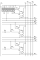
- FIG. 5 is an equivalent circuit diagram of the imaging device shown in FIG. 4;
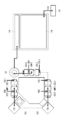
- FIG. 5 is a schematic diagram showing the arrangement of transistors forming a lower electrode and a control section of the imaging element shown in FIG. 4; 5A and 5B are cross-sectional views for explaining a method of manufacturing the imaging element shown in FIG. 4;
- FIG. 9 is a cross-sectional view showing a step following FIG. 8;
- FIG. 10 is a cross-sectional view showing a step following FIG. 9;
- FIG. 11 is a cross-sectional view showing a step following FIG. 10;
- FIG. 12 is a cross-sectional view showing a step following FIG. 11;
- FIG. 13 is a cross-sectional view showing a step following FIG. 12;
- FIG. 5 is a timing chart showing an operation example of the imaging element shown in FIG.
- FIG. 4 It is a cross-sectional schematic diagram showing an example of a configuration of an imaging device according to Modification 1 of the present disclosure. It is a cross-sectional schematic diagram showing an example of a configuration of an imaging device according to Modification 2 of the present disclosure.
- FIG. 12 is a schematic cross-sectional view showing an example of the configuration of an imaging device according to Modification 3 of the present disclosure;
- FIG. 17B is a schematic diagram showing a planar configuration of the imaging element shown in FIG. 17A;
- FIG. 12 is a schematic cross-sectional view showing an example of the configuration of an imaging device according to Modification 4 of the present disclosure;
- FIG. 18B is a schematic diagram showing a planar configuration of the imaging element shown in FIG. 18A.
- FIG. 11 is a schematic cross-sectional view showing another example of the configuration of an imaging device of Modification 2 according to another Modification of the present disclosure
- FIG. 11 is a schematic cross-sectional view showing another example of the configuration of an imaging device of Modification 3 according to another Modification of the present disclosure.
- FIG. 20B is a schematic diagram showing a planar configuration of the imaging element shown in FIG. 20A.
- FIG. 11 is a schematic cross-sectional view showing another example of the configuration of an imaging element of Modification 4 according to another Modification of the present disclosure;
- FIG. 21B is a schematic diagram showing a planar configuration of the imaging device shown in FIG. 21A.
- FIG. 5 is a block diagram showing the overall configuration of an imaging device including the imaging element shown in FIG.
- FIG. 23 is a block diagram showing an example of the configuration of an electronic device using the imaging device shown in FIG. 22;
- FIG. 23 is a schematic diagram showing an example of the overall configuration of a photodetection system using the imaging device shown in FIG. 22;
- FIG. 24B is a diagram showing an example of the circuit configuration of the photodetection system shown in FIG. 24A;
- FIG. It is explanatory drawing showing the example of application of an imaging device.
- 1 is a diagram showing an example of a schematic configuration of an endoscopic surgery system;
- FIG. 3 is a block diagram showing an example of functional configurations of a camera head and a CCU;
- FIG. 1 is a block diagram showing an example of a schematic configuration of a vehicle control system;
- FIG. FIG. 4 is an explanatory diagram showing an example of installation positions of an outside information detection unit and an imaging unit;
- Embodiments (example of photoelectric conversion element provided with a buffer layer having both hole-transporting property and electron-transporting property between the photoelectric conversion layer and the electron injection layer) 1-1.
- Configuration of Photoelectric Conversion Element 1-2. Configuration of image sensor 1-3. Manufacturing method of imaging device 1-4. Signal Acquisition Operation of Imaging Device 1-5. Action and effect 2. Modification 2-1.
- Modification 1 (Another example of the configuration of the imaging element) 2-2.
- Modification 2 (Another example of the configuration of the imaging device) 2-3.
- Modification 3 (Another example of the configuration of the imaging device) 2-4.
- Modification 4 (Another example of the configuration of the imaging device) 2-5.
- Modification 5 (Other Modifications of Imaging Device) 3. Application example 4. Application example 5 .
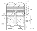
- FIG. 1 schematically illustrates an example of a cross-sectional configuration of a photoelectric conversion element (photoelectric conversion element 10) according to an embodiment of the present disclosure.
- the photoelectric conversion element 10 is, for example, one pixel (unit It is used as an image sensor (image sensor 1A, see FIG. 4, for example) that constitutes the pixel P).
- the photoelectric conversion element 10 has a configuration in which a lower electrode 11, an electron transport layer 12, a photoelectric conversion layer 13, a buffer layer 14, an electron injection layer 15, and an upper electrode 16 are laminated in this order.
- Buffer layer 14 of the present embodiment has both hole-transporting properties and electron-transporting properties.
- the photoelectric conversion element 10 absorbs light corresponding to part or all of wavelengths in a selective wavelength range (for example, a visible light range and a near-infrared light range of 400 nm or more and less than 1300 nm) to generate excitons (electron holes pair).
- a selective wavelength range for example, a visible light range and a near-infrared light range of 400 nm or more and less than 1300 nm
- an imaging element for example, an imaging element 1A
- electrons are read from the lower electrode 11 side as signal charges.
- the configuration and materials of each part will be described, taking as an example the case where electrons are read out from the lower electrode 11 side as signal charges.
- the lower electrode 11 (cathode) is made of, for example, a light-transmitting conductive film.
- the lower electrode 11 has a work function of 4.0 eV or more and 5.5 eV or less.
- the constituent material of the lower electrode 11 include indium tin oxide (ITO), which is In 2 O 3 to which tin (Sn) is added as a dopant.
- ITO indium tin oxide
- Sn tin
- the crystallinity of the ITO thin film may be highly crystalline or low (close to amorphous).
- a tin oxide (SnO 2 )-based material to which a dopant is added for example, ATO to which Sb is added as a dopant, and FTO to which fluorine is added as a dopant can be used.
- zinc oxide (ZnO) or a zinc oxide-based material to which a dopant is added may be used.
- ZnO-based materials include aluminum zinc oxide (AZO) with aluminum (Al) added as a dopant, gallium zinc oxide (GZO) with gallium (Ga) added, and boron zinc oxide with boron (B) added. and indium zinc oxide (IZO) doped with indium (In).
- zinc oxide (IGZO, In-GaZnO 4 ) added with indium and gallium may be used as dopants.
- CuI, InSbO 4 , ZnMgO, CuInO 2 , MgIN 2 O 4 , CdO, ZnSnO 3 , TiO 2 or the like may be used as the constituent material of the lower electrode 11 , spinel oxide or YbFe 2 O may be used.
- An oxide having a tetrastructure may also be used.
- Metals or alloys can be used. Specifically, alkali metals (e.g., lithium (Li), sodium (Na) and potassium (K), etc.) and their fluorides or oxides, alkaline earth metals (e.g., magnesium (Mg) and calcium (Ca) etc.) and their fluorides or oxides.
- Al aluminum
- Al-Si-Cu alloy zinc (Zn), tin (Sn), thallium (Tl), Na-K alloy, Al-Li alloy, Mg-Ag alloy, In and ytterbium (Yb ) and other rare earth metals, or alloys thereof.
- the materials constituting the lower electrode 11 include platinum (Pt), gold (Au), palladium (Pd), chromium (Cr), nickel (Ni), aluminum (Al), silver (Ag), tantalum (Ta ), tungsten (W), copper (Cu), titanium (Ti), indium (In), tin (Sn), iron (Fe), cobalt (Co) and molybdenum (Mo), or their metals Alloys containing elements, conductive particles made of these metals, conductive particles of alloys containing these metals, polysilicon containing impurities, carbon-based materials, oxide semiconductors, carbon nanotubes, graphene, etc. of conductive substances.
- an organic material such as poly(3,4-ethylenedioxythiophene)/polystyrene sulfonic acid [PEDOT/PSS] can be used.
- a paste or ink obtained by mixing the above materials with a binder (polymer) may be cured and used as an electrode.
- the lower electrode 11 can be formed as a single layer film or a laminated film made of the above materials.
- the film thickness of the lower electrode 11 in the stacking direction (hereinafter simply referred to as thickness) is, for example, 20 nm or more and 200 nm or less, preferably 30 nm or more and 150 nm or less.
- the electron transport layer 12 selectively transports electrons among the charges generated in the photoelectric conversion layer 13 to the lower electrode 11 and inhibits injection of holes from the lower electrode 11 side.
- the electron transport layer 12 has a thickness of, for example, 1 nm or more and 60 nm or less.
- the photoelectric conversion layer 13 absorbs, for example, 60% or more of a predetermined wavelength included in at least the visible light region to the near-infrared region, and separates charges.
- the photoelectric conversion layer 13 absorbs light in a part or all of the visible light range and the near-infrared light range of 400 nm or more and less than 1300 nm, for example.
- the photoelectric conversion layer 13 has crystallinity, for example.
- the photoelectric conversion layer 13 includes, for example, two or more kinds of organic materials that function as a p-type semiconductor or an n-type semiconductor. joint surface).
- the photoelectric conversion layer 13 has a laminated structure (p-type semiconductor layer/n-type semiconductor layer) of a layer made of a p-type semiconductor (p-type semiconductor layer) and a layer made of an n-type semiconductor (n-type semiconductor layer), , a stacked structure (p-type semiconductor layer/bulk hetero layer) of a p-type semiconductor layer and a mixed layer (bulk hetero layer) of a p-type semiconductor and an n-type semiconductor (bulk hetero layer), or a stacked structure of an n-type semiconductor layer and a bulk hetero layer ( n-type semiconductor layer/bulk hetero layer).
- it may be formed only by a mixed layer (bulk hetero layer) of a p-type semiconductor and an n-type semiconductor.
- a p-type semiconductor is a hole-transporting material that relatively functions as an electron donor
- an n-type semiconductor is an electron-transporting material that relatively functions as an electron acceptor.
- the photoelectric conversion layer 13 provides a field in which excitons (electron-hole pairs) generated when light is absorbed are separated into electrons and holes. Electrons and holes are separated at the interface (p/n interface) between the donor and the electron acceptor.
- Examples of p-type semiconductors include naphthalene derivatives, anthracene derivatives, phenanthrene derivatives, pyrene derivatives, perylene derivatives, tetracene derivatives, pentacene derivatives, quinacridone derivatives, thiophene derivatives, thienothiophene derivatives, benzothiophene derivatives, and benzothienobenzothiophene (BTBT).
- triphenylamine derivatives for example, fluoranthene derivatives, phthalocyanine derivatives, subphthalocyanine derivatives, subporphyrazine derivatives, metals having heterocyclic compounds as ligands complexes, polythiophene derivatives, polybenzothiadiazole derivatives, polyfluorene derivatives and the like.
- n-type semiconductors include fullerenes represented by higher order fullerenes such as fullerene C 60 , fullerene C 70 and fullerene C 74 and endohedral fullerenes, and derivatives thereof.
- Substituents contained in fullerene derivatives include, for example, halogen atoms, linear or branched or cyclic alkyl groups or phenyl groups, linear or condensed aromatic compound-containing groups, halide-containing groups, partial fluoroalkyl groups, perfluoroalkyl groups, silylalkyl groups, silylalkoxy groups, arylsilyl groups, arylsulfanyl groups, alkylsulfanyl groups, arylsulfonyl groups, alkylsulfonyl groups, arylsulfide groups, alkylsulfide groups, amino groups, alkylamino groups, arylamino group, hydroxy group, alkoxy group, acylamino group, acyloxy group, carbonyl group, carboxy group, carboxoamide group, carboalkoxy group, acyl group, sulfonyl group, cyano group, nitro group, group having chal
- fullerene derivatives include, for example, fullerene fluorides, PCBM fullerene compounds, and fullerene multimers.
- n-type semiconductors include organic semiconductors with higher (deeper) HOMO (Highest Occupied Molecular Orbital) levels and LUMO (Lowest Unoccupied Molecular Orbital) levels than p-type semiconductors, and inorganic metal oxides with optical transparency. is mentioned.
- n-type organic semiconductors include heterocyclic compounds containing nitrogen atoms, oxygen atoms or sulfur atoms.
- examples include organic molecules, organometall
- the photoelectric conversion layer 13 includes, in addition to the p-type semiconductor and the n-type semiconductor, an organic material that absorbs light in a predetermined wavelength range and transmits light in other wavelength ranges, that is, a dye material.
- a dye material may be Pigment materials include, for example, subphthalocyanine derivatives.
- dye materials include, for example, porphyrin, phthalocyanine, dipyrromethane, azadipyrromethane, dipyridyl, azadipyridyl, coumarin, perylene, perylene diimide, pyrene, naphthalene diimide, quinacridone, xanthene, xanthenoxanthene, phenoxazine, indigo, azo, Oxazines, benzodithiophenes, naphthodithiophenes, anthradithiophenes, rubicene, anthracenes, tetracenes, pentacenes, anthraquinones, tetraquinones, pentaquinones, dinaphthothienothiophenes, diketopyrrolopyrroles, oligothiophenes, cyanines, merocyanines, squalium, croconium and boron -
- the photoelectric conversion layer 13 is formed using three kinds of organic materials, ie, a p-type semiconductor, an n-type semiconductor, and a dye material
- the p-type semiconductor and the n-type semiconductor are materials having optical transparency in the visible light region.
- the photoelectric conversion layer 13 selectively photoelectrically converts light in the wavelength range absorbed by the dye material.
- the photoelectric conversion layer 13 has a thickness of, for example, 10 nm or more and 500 nm or less, preferably 100 nm or more and 400 nm or less.
- the buffer layer 14 selectively transports holes among the charges generated in the photoelectric conversion layer 13 to the upper electrode 16 and inhibits injection of electrons from the upper electrode 16 side.
- the buffer layer 14 has both hole-transporting properties and electron-transporting properties.
- buffer layer 14 has a hole mobility of 10 ⁇ 6 cm 2 /Vs or greater and an electron mobility of 10 ⁇ 6 cm 2 /Vs or greater.
- FIG. 2 shows an example of energy levels of the photoelectric conversion layer 13, the buffer layer 14, the electron injection layer 15, and the upper electrode 16 that constitute the photoelectric conversion element 10 shown in FIG.
- the buffer layer 14 preferably also has the following relationship with each adjacent layer.
- the difference between the HOMO level of the buffer layer 14 and the HOMO level of the photoelectric conversion layer 13 is preferably ⁇ 0.4 eV or less.
- the energy barrier at the interface between the buffer layer 14 and the electron injection layer 15 is preferably large.
- the difference between the LUMO level of the buffer layer 14 and the LUMO level of the electron injection layer 15 is 1.0 eV or more.
- the difference between the electron mobility of the buffer layer 14 and the electron mobility of the electron injection layer 15 is preferably 10 ⁇ 3 cm 2 /Vs or more.
- the charge blocking property at the interface between the buffer layer 14 and the electron injection layer 15 is further improved, and the generation of dark current is reduced.
- the charge recombination rate at the interface between the buffer layer 14 and the electron injection layer 15 is improved, and the afterimage characteristics are improved.
- the buffer layer 14 having the properties described above can be formed using, for example, one or more charge-transporting materials that have both hole-transporting properties and electron-transporting properties.
- charge-transporting materials include organic semiconductor materials containing ⁇ -electron-rich heterocycles and ⁇ -electron-deficient heterocycles in their molecules.
- ⁇ -electron rich heterocyclic ring examples include pyrrole represented by the following formula (1), furan represented by the following formula (2), thiophene represented by the following formula (3), and indole represented by the following formula (4). be done.
- Examples of the ⁇ -electron-deficient heterocyclic ring include pyridine represented by the following formula (5), pyrimidine represented by the following formula (6), quinoline represented by the following formula (7), pyrrole represented by the following formula (8), and the following Examples include isoquinolines represented by formula (9).
- organic semiconductor materials containing ⁇ -electron-rich heterocycles and ⁇ -electron-deficient heterocycles include 9-(4,6-diphenyl-1,3,5-triazine- 2-yl)-9′-phenyl-3,3′-bi[9H-carbazole] (PCCzTzn, formula (9)), 3-[9,9-dimethylacridin-10(9H)-yl]-9H- xanthen-9-one (ACRXTN, formula (11)) and bis[4-[9,9-dimethylacridin-10(9H)-yl]phenyl]sulfone (DMAC-DPS, formula (12)).
- the buffer layer 14 is a single-layer film made of one type of charge-transporting material having both hole-transporting properties and electron-transporting properties, or two or more types of charge-transporting materials having both hole-transporting properties and electron-transporting properties. It can be formed as a mixed film of materials. Note that the buffer layer 14 may contain materials other than the charge transport material described above.
- the buffer layer 14 has a thickness of, for example, 5 nm or more and 100 nm or less, preferably 5 nm or more and 50 nm or less. More preferably, buffer layer 14 has a thickness of 5 nm or more and 20 nm or less.
- the electron injection layer 15 promotes injection of electrons from the upper electrode 16 .
- the electron injection layer 15 has an electron affinity greater than the work function of the upper electrode 16 and improves electrical bonding between the buffer layer 14 and the upper electrode 16 .
- Materials constituting the electron injection layer 15 include, for example, dipyrazino[2,3-f:2′,3′vh]quinoxaline-2,3,6,7,10,11-hexacarbonitrile (HATCN). is mentioned.
- materials constituting the electron injection layer 15 include PEDOT/PSS, polyaniline, and metal oxides such as MoO x , RuO x , VO x and WO x .
- the upper electrode 16 (anode), like the lower electrode 11, is made of, for example, a light-transmitting conductive film.
- the constituent material of the upper electrode 16 include indium tin oxide (ITO), which is In 2 O 3 to which tin (Sn) is added as a dopant.
- ITO indium tin oxide
- the crystallinity of the ITO thin film may be highly crystalline or low (close to amorphous).
- a tin oxide (SnO 2 )-based material to which a dopant is added for example, ATO to which Sb is added as a dopant, and FTO to which fluorine is added as a dopant can be used.
- ZnO zinc oxide
- ZnO-based materials include aluminum zinc oxide (AZO) with aluminum (Al) added as a dopant, gallium zinc oxide (GZO) with gallium (Ga) added, and boron zinc oxide with boron (B) added. and indium zinc oxide (IZO) doped with indium (In).
- zinc oxide (IGZO, In--GaZnO 4 ) added with indium and gallium may be used as a dopant.
- CuI, InSbO 4 , ZnMgO, CuInO 2 , MgIN 2 O 4 , CdO, ZnSnO 3 , TiO 2 or the like may be used as the constituent material of the upper electrode 16 , spinel oxide or YbFe 2 O may be used. An oxide having a tetrastructure may also be used.
- the material constituting the upper electrode 16 includes metals such as Pt, Au, Pd, Cr, Ni, Al, Ag, Ta, W, Cu, Ti, In, Sn, Fe, Co and Mo, or alloys containing metal elements, or conductive particles made of these metals, conductive particles of alloys containing these metals, polysilicon containing impurities, carbon-based materials, oxide semiconductors, carbon nanotubes, Conductive substances such as graphene can be used.
- organic materials (conductive polymers) such as PEDOT/PSS can be used as materials for forming the upper electrode 16 .
- a paste or ink obtained by mixing the above materials with a binder (polymer) may be cured and used as an electrode.
- the upper electrode 16 can be formed as a single layer film or a laminated film made of the above materials.
- the thickness of the upper electrode 16 is, for example, 20 nm or more and 200 nm or less, preferably 30 nm or more and 150 nm or less.
- the photoelectric conversion element 10 shown in FIG. 1 is shown as an example in which electrons are read out as signal charges from the lower electrode 11 side, it is not limited to this.
- a buffer layer 14, a photoelectric conversion layer 13, and an electron transport layer 12 are laminated in this order from the lower electrode 11 side between a lower electrode 11 and an upper electrode 16.
- the buffer layer 14 preferably has a hole mobility of 10 ⁇ 6 cm 2 /Vs or more and an electron mobility of 10 ⁇ 6 cm 2 /Vs or more.
- the difference between the energy level of the buffer layer 14 and the energy level of the photoelectric conversion layer 13 is preferably ⁇ 0.4 eV or less.
- the energy barrier at the interface between the buffer layer 14 and the adjacent lower electrode 11 is preferably large.
- the difference between the LUMO level of the buffer layer 14 and the LUMO level of the adjacent lower electrode 11 is 1.0 eV. It is preferable that it is above.
- the difference between the electron mobility of the buffer layer 14 and the electron mobility of the adjacent lower electrode 11 is preferably 10 ⁇ 3 cm 2 /Vs or more. This further improves the charge blocking property and reduces the generation of dark current. In addition, the charge recombination rate between the buffer layer 14 and the adjacent lower electrode 11 is improved, and the afterimage characteristics are improved.
- the electron transport layer 12 is not necessarily provided. , other layers may be further provided in addition to the buffer layer 14 and the electron injection layer 15 .
- an undercoat layer may be provided in addition to the electron transport layer 12, and between the electron injection layer 15 and the upper electrode 16, an electron A transport layer may be provided.
- the light incident on the photoelectric conversion element 10 is absorbed in the photoelectric conversion layer 13 .
- the excitons (electron-hole pairs) generated by this are exciton-separated at the interface (p/n junction surface) between the p-type semiconductor and the n-type semiconductor constituting the photoelectric conversion layer 13, that is, the electrons and holes dissociate to
- the carriers (electrons and holes) generated here are transported to different electrodes by diffusion due to the difference in carrier concentration and the internal electric field due to the difference in work function between the anode and the cathode, and are detected as photocurrent.
- electrons separated at the p/n junction are extracted from the lower electrode 11 via the electron transport layer 12 .
- Holes separated at the p/n junction are extracted from the upper electrode 16 via the buffer layer 14 and the electron injection layer 15 .
- the transport direction of electrons and holes can also be controlled by applying a potential between the lower electrode 11 and the upper electrode 16 .
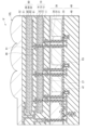
- FIG. 4 schematically shows an example of a cross-sectional configuration of an imaging device (imaging device 1A) using the photoelectric conversion device 10 described above.
- FIG. 5 schematically shows an example of the planar configuration of the imaging device 1A shown in FIG. 4, and FIG. 4 shows a cross section taken along line II shown in FIG.
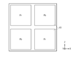
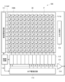
- the imaging device 1A constitutes, for example, one pixel (unit pixel P) that is repeatedly arranged in an array in the pixel section 100A of the imaging device 100 shown in FIG.
- a pixel unit 1a composed of four pixels arranged in two rows and two columns is a repeating unit, and is repeatedly arranged in an array in the row direction and the column direction. ing.
- the imaging device 1A selectively detects light in mutually different wavelength ranges and performs photoelectric conversion.
- one photoelectric conversion unit formed using an organic material and two photoelectric conversion units are vertically laminated, so-called vertical direction spectral type.
- the photoelectric conversion element 10 described above can be used as a photoelectric conversion section that constitutes the imaging element 1A.
- the photoelectric conversion unit has the same configuration as the photoelectric conversion element 10 described above, and is denoted by the same reference numeral 10. As shown in FIG.
- the photoelectric conversion section 10 is provided on the back surface (first surface 30S1) side of the semiconductor substrate 30.
- the photoelectric conversion regions 32B and 32R are embedded in the semiconductor substrate 30 and stacked in the thickness direction of the semiconductor substrate 30 .
- the photoelectric conversion section 10 and the photoelectric conversion regions 32B and 32R selectively detect light in mutually different wavelength ranges and perform photoelectric conversion.
- the photoelectric conversion unit 10 acquires a green (G) color signal.
- the photoelectric conversion regions 32B and 32R acquire blue (B) and red (R) color signals, respectively, due to the difference in absorption coefficient.
- the imaging device 1A can acquire a plurality of types of color signals in one pixel without using a color filter.
- the semiconductor substrate 30 is composed of an n-type silicon (Si) substrate, for example, and has a p-well 31 in a predetermined region.
- various floating diffusions (floating diffusion layers) FD eg, FD1, FD2, FD3
- various transistors Tr eg, vertical transistors ( A transfer transistor Tr2, a transfer transistor Tr3, an amplifier transistor (modulation element) AMP and a reset transistor RST) are provided.
- a multilayer wiring layer 40 is further provided on the second surface 30S2 of the semiconductor substrate 30 with the gate insulating layer 33 interposed therebetween.
- the multilayer wiring layer 40 has, for example, a structure in which wiring layers 41 , 42 and 43 are laminated within an insulating layer 44 .
- a peripheral circuit (not shown) including a logic circuit or the like is provided in the peripheral portion of the semiconductor substrate 30 .
- a protective layer 51 is provided above the photoelectric conversion section 10 .
- wiring is provided to electrically connect the upper electrode 16 and the peripheral circuit section around the light shielding film 53 and the pixel section 100A.
- Optical members such as a planarizing layer (not shown) and an on-chip lens 52L are further provided above the protective layer 51 .
- the first surface 30S1 side of the semiconductor substrate 30 is represented as the light incident surface S1
- the second surface 30S2 side is represented as the wiring layer side S2.
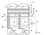
- an electron transport layer 12, a photoelectric conversion layer 13, a buffer layer 14 and an electron injection layer 15 are laminated in this order between a lower electrode 11 and an upper electrode 16 which are arranged to face each other.
- the lower electrode 11 is composed of a plurality of electrodes (for example, two readout electrodes 11A and storage electrodes 11B).
- Semiconductor layers 18 are laminated in this order.
- the readout electrode 11A is electrically connected to the semiconductor layer 18 through an opening 17H provided in the insulating layer 17 .
- the readout electrode 11A is for transferring charges generated in the photoelectric conversion layer 13 to the floating diffusion FD1. It is connected to the floating diffusion FD1 via the electrode 34, the connection portion 41A and the lower second contact 46.
- the accumulation electrode 11B is for accumulating electrons among charges generated in the photoelectric conversion layer 13 in the semiconductor layer 18 as signal charges.
- the storage electrode 11B is provided in a region facing the light receiving surfaces of the photoelectric conversion regions 32B and 32R formed in the semiconductor substrate 30 and covering these light receiving surfaces.
- the storage electrode 11B is preferably larger than the readout electrode 11A, so that more charge can be stored.
- the voltage application section 54 is connected to the storage electrode 11B via wiring such as the upper third contact 24C and the pad section 39C.
- a pixel separation electrode 28 is provided around each pixel unit 1a repeatedly arranged in an array. A predetermined potential is applied to the pixel isolation electrode 28, and the adjacent pixel units 1a are electrically isolated from each other.
- the insulating layer 17 is for electrically separating the storage electrode 11B and the semiconductor layer 18 from each other.
- the insulating layer 17 is provided, for example, on the interlayer insulating layer 23 so as to cover the lower electrode 11 .
- the insulating layer 17 is, for example, a single layer film made of one of silicon oxide (SiO x ), silicon nitride (SiN x ) and silicon oxynitride (SiO x N y ), or two of these. It is composed of a laminated film composed of the above.
- the thickness of the insulating layer 17 is, for example, 20 nm or more and 500 nm or less.
- the semiconductor layer 18 is for accumulating signal charges generated in the photoelectric conversion layer 13 .
- the semiconductor layer 18 is preferably formed using a material having a higher charge mobility and a larger bandgap than the photoelectric conversion layer 13 .
- the bandgap of the constituent material of the semiconductor layer 18 is preferably 3.0 eV or more.
- oxide semiconductors such as IGZO and organic semiconductors.
- organic semiconductors include transition metal dichalcogenides, silicon carbide, diamond, graphene, carbon nanotubes, condensed polycyclic hydrocarbon compounds and condensed heterocyclic compounds.
- the thickness of the semiconductor layer 18 is, for example, 10 nm or more and 300 nm or less.
- the semiconductor layer 18, the electron transport layer 12, the photoelectric conversion layer 13, the buffer layer 14, the electron injection layer 15, and the upper electrode 16 are provided as continuous layers common to a plurality of pixels (unit pixel P). is shown, but is not limited to this.
- the semiconductor layer 18, the electron transport layer 12, the photoelectric conversion layer 13, the buffer layer 14, the electron injection layer 15 and the upper electrode 16 may be formed separately for each unit pixel P, for example.
- a layer having fixed charges (fixed charge layer) 21 , a dielectric layer 22 having insulating properties, and an interlayer insulating layer 23 are arranged as first layers of the semiconductor substrate 30 . They are provided in this order from the first surface 30S1 side.
- the fixed charge layer 21 may be a film having positive fixed charges or a film having negative fixed charges.
- a constituent material of the fixed charge layer 21 it is preferable to use a semiconductor or a conductive material having a wider bandgap than the semiconductor substrate 30 is used. Thereby, generation of dark current at the interface of the semiconductor substrate 30 can be suppressed.
- constituent materials of the fixed charge layer 21 include hafnium oxide (HfO x ), aluminum oxide (AlO x ), zirconium oxide (ZrO x ), tantalum oxide (TaO x ), titanium oxide (TiO x ), lanthanum oxide ( LaO x ), praseodymium oxide (PrO x ), cerium oxide (CeO x ), neodymium oxide (NdO x ), promethium oxide (PmO x ), samarium oxide (SmO x ), europium oxide (EuO x ) , gadolinium oxide (GdO x ), terbium oxide (TbO x ), dysprosium oxide (DyO x ), holmium oxide (HoO x ), thulium oxide (TmO x ) , ytterbium oxide (YbO x ), lutetium oxide (LuO x
- the dielectric layer 22 is for preventing light reflection caused by a refractive index difference between the semiconductor substrate 30 and the interlayer insulating layer 23 .
- a material having a refractive index between that of the semiconductor substrate 30 and that of the interlayer insulating layer 23 is preferable.
- constituent materials of the dielectric layer 22 include SiO x , TEOS, SiN x and SiO x N y .
- the interlayer insulating layer 23 is composed of, for example, a single layer film made of one of SiO x , SiN x and SiO x N y or the like, or a laminated film made of two or more of these.
- the photoelectric conversion regions 32B and 32R are composed of, for example, PIN (Positive Intrinsic Negative) type photodiodes, and each have a pn junction in a predetermined region of the semiconductor substrate 30.
- the photoelectric conversion regions 32B and 32R make it possible to disperse the light in the vertical direction by utilizing the fact that the wavelength regions absorbed by the silicon substrate differ depending on the incident depth of the light.
- the photoelectric conversion region 32B selectively detects blue light and accumulates signal charges corresponding to blue, and is formed to a depth that enables efficient photoelectric conversion of blue light.
- the photoelectric conversion region 32R selectively detects red light and accumulates signal charges corresponding to red, and is formed to a depth that enables efficient photoelectric conversion of red light.
- Blue (B) is a color corresponding to, for example, a wavelength range of 400 nm or more and less than 495 nm
- red (R) is a color corresponding to, for example, a wavelength range of 620 nm or more and less than 750 nm.
- Each of the photoelectric conversion regions 32B and 32R should be capable of detecting light in a part or all of the wavelength bands.
- the photoelectric conversion region 32B and the photoelectric conversion region 32R each have, for example, a p+ region serving as a hole accumulation layer and an n region serving as an electron accumulation layer (p -np stacked structure).
- the n region of the photoelectric conversion region 32B is connected to the vertical transistor Tr2.
- the p+ region of the photoelectric conversion region 32B is bent along the vertical transistor Tr2 and connected to the p+ region of the photoelectric conversion region 32R.
- the gate insulating layer 33 is composed of, for example, a single layer film made of one of SiO x , SiN x and SiO x N y or the like, or a laminated film made of two or more of these.
- a through electrode 34 is provided between the first surface 30S1 and the second surface 30S2 of the semiconductor substrate 30 .
- the through electrode 34 functions as a connector between the photoelectric conversion section 10 and the gate Gamp of the amplifier transistor AMP and the floating diffusion FD1, and also serves as a transmission path for charges generated in the photoelectric conversion section 10 .
- a reset gate Grst of the reset transistor RST is arranged next to the floating diffusion FD1 (one source/drain region 36B of the reset transistor RST). As a result, the charges accumulated in the floating diffusion FD1 can be reset by the reset transistor RST.
- the upper end of the through electrode 34 is connected to the readout electrode 11A via, for example, a pad portion 39A provided in the interlayer insulating layer 23, an upper first contact 24A, a pad electrode 38B and an upper second contact 24B.
- a lower end of the through-electrode 34 is connected to a connecting portion 41A in the wiring layer 41, and the connecting portion 41A and the gate Gamp of the amplifier transistor AMP are connected via a lower first contact 45.
- the connection portion 41A and the floating diffusion FD1 (region 36B) are connected via the lower second contact 46, for example.
- Upper first contact 24A, upper second contact 24B, upper third contact 24C, pad portions 39A, 39B, 39C, wiring layers 41, 42, 43, lower first contact 45, lower second contact 46, and gate wiring layer 47 can be formed using, for example, doped silicon materials such as PDAS (Phosphorus Doped Amorphous Silicon), or metallic materials such as Al, W, Ti, Co, Hf and Ta.
- doped silicon materials such as PDAS (Phosphorus Doped Amorphous Silicon)
- metallic materials such as Al, W, Ti, Co, Hf and Ta.
- the insulating layer 44 is composed of, for example, a single layer film made of one of SiO x , SiN x and SiO x N y or the like, or a laminated film made of two or more of these.
- the protective layer 51 and the on-chip lens 52L are made of a light-transmissive material, such as a single-layer film made of one of SiO x , SiN x and SiO x N y , or a combination of these. It is composed of a laminated film consisting of two or more of them.
- the thickness of the protective layer 51 is, for example, 100 nm or more and 30000 nm or less.
- the light shielding film 53 is provided, for example, so as to cover at least the region of the readout electrode 21A that is in direct contact with the semiconductor layer 18 without covering the storage electrode 11B.
- the light shielding film 53 can be formed using, for example, W, Al, an alloy of Al and Cu, or the like.
- FIG. 6 is an equivalent circuit diagram of the imaging device 1A shown in FIG.
- FIG. 7 schematically shows the arrangement of the transistors that constitute the lower electrode 11 and the control section of the imaging device 1A shown in FIG.
- the reset transistor RST (reset transistor TR1rst) is for resetting the charge transferred from the photoelectric conversion section 10 to the floating diffusion FD1, and is composed of, for example, a MOS transistor.
- the reset transistor TR1rst is composed of a reset gate Grst, a channel formation region 36A, and source/drain regions 36B and 36C.
- the reset gate Grst is connected to the reset line RST1, and one source/drain region 36B of the reset transistor TR1rst also serves as the floating diffusion FD1.
- the other source/drain region 36C forming the reset transistor TR1rst is connected to the power supply line VDD.
- the amplifier transistor AMP is a modulation element that modulates the amount of charge generated in the photoelectric conversion section 10 into voltage, and is composed of, for example, a MOS transistor. Specifically, the amplifier transistor AMP is composed of a gate Gamp, a channel forming region 35A, and source/drain regions 35B and 35C.
- the gate Gamp is connected to the readout electrode 11A and one of the source/drain regions 36B (floating diffusion FD1) of the reset transistor TR1rst via the lower first contact 45, the connecting portion 41A, the lower second contact 46, the through electrode 34, and the like. It is One source/drain region 35B shares a region with the other source/drain region 36C forming the reset transistor TR1rst, and is connected to the power supply line VDD.
- the selection transistor SEL selection transistor TR1sel
- the selection transistor SEL is composed of a gate Gsel, a channel forming region 34A, and source/drain regions 34B and 34C.
- the gate Gsel is connected to the selection line SEL1.
- One source/drain region 34B shares a region with the other source/drain region 35C forming the amplifier transistor AMP, and the other source/drain region 34C is connected to the signal line (data output line) VSL1. It is
- the transfer transistor TR2 (transfer transistor TR2trs) is for transferring the signal charge corresponding to blue generated and accumulated in the photoelectric conversion region 32B to the floating diffusion FD2. Since the photoelectric conversion region 32B is formed deep from the second surface 30S2 of the semiconductor substrate 30, the transfer transistor TR2trs of the photoelectric conversion region 32B is preferably configured by a vertical transistor. The transfer transistor TR2trs is connected to the transfer gate line TG2. A floating diffusion FD2 is provided in a region 37C near the gate Gtrs2 of the transfer transistor TR2trs. The charge accumulated in the photoelectric conversion region 32B is read out to the floating diffusion FD2 through the transfer channel formed along the gate Gtrs2.
- the transfer transistor TR3 (transfer transistor TR3trs) is for transferring the signal charge corresponding to red generated and accumulated in the photoelectric conversion region 32R to the floating diffusion FD3, and is composed of, for example, a MOS transistor.
- the transfer transistor TR3trs is connected to the transfer gate line TG3.
- a floating diffusion FD3 is provided in a region 38C near the gate Gtrs3 of the transfer transistor TR3trs. The charge accumulated in the photoelectric conversion region 32R is read out to the floating diffusion FD3 through the transfer channel formed along the gate Gtrs3.
- a reset transistor TR2rst an amplifier transistor TR2amp, and a select transistor TR2sel, which constitute a control section of the photoelectric conversion region 32B, are provided. Furthermore, a reset transistor TR3rst, an amplifier transistor TR3amp, and a selection transistor TR3sel, which constitute a control section of the photoelectric conversion region 32R, are provided.
- the reset transistor TR2rst is composed of a gate, a channel forming region and source/drain regions.
- a gate of the reset transistor TR2rst is connected to the reset line RST2, and one source/drain region of the reset transistor TR2rst is connected to the power supply line VDD.
- the other source/drain region of the reset transistor TR2rst also serves as the floating diffusion FD2.
- the amplifier transistor TR2amp is composed of a gate, a channel forming region and source/drain regions.
- a gate is connected to the other source/drain region (floating diffusion FD2) of the reset transistor TR2rst.
- One source/drain region forming the amplifier transistor TR2amp shares a region with one source/drain region forming the reset transistor TR2rst, and is connected to the power supply line VDD.
- the selection transistor TR2sel is composed of a gate, a channel forming region and source/drain regions.
- the gate is connected to the selection line SEL2.
- One source/drain region forming the select transistor TR2sel shares a region with the other source/drain region forming the amplifier transistor TR2amp.
- the other source/drain region forming the select transistor TR2sel is connected to the signal line (data output line) VSL2.
- the reset transistor TR3rst is composed of a gate, a channel forming region and source/drain regions.
- a gate of the reset transistor TR3rst is connected to the reset line RST3, and one source/drain region forming the reset transistor TR3rst is connected to the power supply line VDD.
- the other source/drain region forming the reset transistor TR3rst also serves as the floating diffusion FD3.
- the amplifier transistor TR3amp is composed of a gate, a channel forming region and source/drain regions.
- the gate is connected to the other source/drain region (floating diffusion FD3) forming the reset transistor TR3rst.
- One source/drain region forming the amplifier transistor TR3amp shares a region with one source/drain region forming the reset transistor TR3rst, and is connected to the power supply line VDD.
- the select transistor TR3sel is composed of a gate, a channel forming region and source/drain regions.
- the gate is connected to the selection line SEL3.
- One source/drain region forming the select transistor TR3sel shares a region with the other source/drain region forming the amplifier transistor TR3amp.
- the other source/drain region forming the select transistor TR3sel is connected to the signal line (data output line) VSL3.
- the reset lines RST1, RST2, and RST3, the selection lines SEL1, SEL2, and SEL3, and the transfer gate lines TG2 and TG3 are each connected to a vertical drive circuit forming a drive circuit.
- the signal lines (data output lines) VSL1, VSL2 and VSL3 are connected to a column signal processing circuit 112 that constitutes a drive circuit.
- the imaging device 1A of this embodiment can be manufactured, for example, as follows.
- a p-well 31 is formed in a semiconductor substrate 30, and in this p-well 31, for example, n-type photoelectric conversion regions 32B and 32R are formed.
- a p+ region is formed near the first surface 30S1 of the semiconductor substrate 30 .
- the transfer transistors Tr2, the transfer transistors Tr3, and the selection gate are formed on the second surface 30S2 of the semiconductor substrate 30, as shown in FIG. 8, for example, after forming n+ regions to be the floating diffusions FD1 to FD3, the gate insulating layer 33, the transfer transistors Tr2, the transfer transistors Tr3, and the selection gate are formed.
- a gate wiring layer 47 including gates of the transistor SEL, amplifier transistor AMP and reset transistor RST is formed.
- a transfer transistor Tr2, a transfer transistor Tr3, a select transistor SEL, an amplifier transistor AMP, and a reset transistor RST are formed on the second surface 30S2 of the semiconductor substrate 30, the multilayer wiring layer 40 composed of the wiring layers 41 to 43 including the lower first contact 45, the lower second contact 46 and the connecting portion 41A and the insulating layer 44 is formed.
- an SOI (Silicon on Insulator) substrate in which the semiconductor substrate 30, a buried oxide film (not shown), and a holding substrate (not shown) are laminated is used as the base of the semiconductor substrate 30, for example.
- the buried oxide film and the holding substrate are bonded to the first surface 30S1 of the semiconductor substrate 30, although not shown in FIG. Annealing is performed after the ion implantation.
- a support substrate (not shown) or another semiconductor substrate or the like is bonded onto the multilayer wiring layer 40 provided on the second surface 30S2 side of the semiconductor substrate 30 and turned upside down. Subsequently, the semiconductor substrate 30 is separated from the embedded oxide film of the SOI substrate and the holding substrate, and the first surface 30S1 of the semiconductor substrate 30 is exposed.
- the above steps can be performed by techniques such as ion implantation and CVD (Chemical Vapor Deposition), which are used in ordinary CMOS processes.
- the semiconductor substrate 30 is processed from the first surface 30S1 side by dry etching, for example, to form, for example, an annular opening 34H.
- the depth of the opening 34H is such that it penetrates from the first surface 30S1 to the second surface 30S2 of the semiconductor substrate 30 and reaches, for example, the connection portion 41A.
- the negative fixed charge layer 21 and the dielectric layer 22 are sequentially formed on the first surface 30S1 of the semiconductor substrate 30 and the side surfaces of the openings 34H.
- the fixed charge layer 21 can be formed, for example, by forming an HfOx film using an atomic layer deposition method (ALD method).
- the dielectric layer 22 can be formed, for example, by depositing a SiOx film using a plasma CVD method.
- a pad portion 39A is formed by laminating a barrier metal made of, for example, a laminated film of titanium and titanium nitride (Ti/TiN film) and a W film.
- an interlayer insulating layer 23 is formed on the dielectric layer 22 and the pad portion 39A, and the surface of the interlayer insulating layer 23 is planarized using a CMP (Chemical Mechanical Polishing) method.
- CMP Chemical Mechanical Polishing
- the opening 23H1 is filled with a conductive material such as Al to form the upper first contact 24A.
- a conductive material such as Al
- pad portions 39B and 39C are formed in the same manner as pad portion 39A, interlayer insulating layer 23, upper second contact 24B and upper third contact 24C are formed in this order.
- a conductive film 11X is formed on the interlayer insulating layer 23 by, for example, sputtering, and then patterned by photolithography. Specifically, after forming a photoresist PR at a predetermined position of the conductive film 11X, the conductive film 11X is processed using dry etching or wet etching. After that, by removing the photoresist PR, the readout electrode 11A and the storage electrode 11B are formed as shown in FIG.
- an insulating layer 17, a semiconductor layer 18, an electron transport layer 12, a photoelectric conversion layer 13, a buffer layer 14, an electron injection layer 15 and an upper electrode 16 are formed in order.
- the insulating layer 17 for example, after forming a SiOx film using the ALD method, the surface of the insulating layer 17 is planarized using the CMP method. After that, an opening 17H is formed on the readout electrode 11A using wet etching, for example.
- the semiconductor layer 18 can be formed using, for example, a sputtering method.
- the electron transport layer 12, the photoelectric conversion layer 13, the buffer layer 14, and the electron injection layer 15 are formed using, for example, a vacuum deposition method.
- the upper electrode 16 is formed using, for example, sputtering, similarly to the lower electrode 11 . Finally, on the upper electrode 16, the protective layer 51, the light shielding film 53 and the on-chip lens 52L are arranged. As described above, the imaging device 1A shown in FIG. 4 is completed.
- the electron transport layer 12, the photoelectric conversion layer 13, the buffer layer 14, and the electron injection layer 15 are desirably formed continuously in a vacuum process (an integrated vacuum process). Further, the organic layers such as the electron transport layer 12, the photoelectric conversion layer 13, the buffer layer 14 and the electron injection layer 15 and the conductive films such as the lower electrode 11 and the upper electrode 16 are formed using a dry film forming method or a wet film forming method. can be formed.
- the dry film forming method in addition to the vacuum deposition method using resistance heating or high frequency heating, the electron beam (EB) deposition method, various sputtering methods (magnetron sputtering method, RF-DC coupled bias sputtering method, ECR sputtering method) , facing target sputtering method, high frequency sputtering method), ion plating method, laser abrasion method, molecular beam epitaxy method and laser transfer method.
- dry film formation methods include chemical vapor deposition methods such as plasma CVD, thermal CVD, MOCVD, and optical CVD.
- Wet film-forming methods include spin coating, inkjet, spray coating, stamping, microcontact printing, flexographic printing, offset printing, gravure printing, and dipping.
- etching in addition to photolithography, chemical etching such as shadow mask and laser transfer, physical etching using ultraviolet rays, laser, etc. can be used.
- a flattening technique in addition to the CMP method, a laser flattening method, a reflow method, or the like can be used.
- green light (G) is first selectively detected (absorbed) and photoelectrically converted by the photoelectric conversion section 10 .
- the photoelectric conversion unit 10 is connected to the gate Gamp of the amplifier transistor AMP and the floating diffusion FD1 via the through electrode 34. Therefore, electrons among excitons generated in the photoelectric conversion part 10 are extracted from the lower electrode 11 side, transferred to the second surface 30S2 side of the semiconductor substrate 30 via the through electrode 34, and accumulated in the floating diffusion FD1. . At the same time, the amount of charge generated in the photoelectric conversion section 10 is modulated into a voltage by the amplifier transistor AMP.
- a reset gate Grst of the reset transistor RST is arranged next to the floating diffusion FD1. As a result, the charges accumulated in the floating diffusion FD1 are reset by the reset transistor RST.
- the photoelectric conversion section 10 is connected not only to the amplifier transistor AMP but also to the floating diffusion FD1 via the through electrode 34, the charge accumulated in the floating diffusion FD1 can be easily reset by the reset transistor RST. becomes.
- FIG. 14 shows an operation example of the imaging device 1A.
- A shows the potential at the storage electrode 11B
- B shows the potential at the floating diffusion FD1 (readout electrode 11A)
- C shows the potential at the gate (Gsel) of the reset transistor TR1rst. is.
- voltages are individually applied to the readout electrode 11A and the storage electrode 11B.
- the potential V1 is applied from the drive circuit to the readout electrode 11A and the potential V2 is applied to the storage electrode 11B during the accumulation period.
- the potentials V1 and V2 are V2>V1.
- charges (signal charges; electrons) generated by photoelectric conversion are attracted to the storage electrode 11B and accumulated in the region of the semiconductor layer 18 facing the storage electrode 11B (accumulation period).
- the potential of the region of the semiconductor layer 18 facing the storage electrode 11B becomes a more negative value as the photoelectric conversion time elapses. Holes are sent from the upper electrode 16 to the driving circuit.
- a reset operation is performed in the latter half of the accumulation period. Specifically, at timing t1, the scanning unit changes the voltage of the reset signal RST from low level to high level. Thereby, in the unit pixel P, the reset transistor TR1rst is turned on, and as a result, the voltage of the floating diffusion FD1 is set to the power supply voltage, and the voltage of the floating diffusion FD1 is reset (reset period).
- the drive circuit applies a potential V3 to the readout electrode 11A and a potential V4 to the storage electrode 11B.
- the potentials V3 and V4 are V3 ⁇ V4.
- the charges accumulated in the region corresponding to the storage electrode 11B are read from the readout electrode 11A to the floating diffusion FD1. That is, the charges accumulated in the semiconductor layer 18 are read out to the control section (transfer period).
- the potential V1 is applied again from the drive circuit to the readout electrode 11A, and the potential V2 is applied to the storage electrode 11B.
- charges generated by photoelectric conversion are attracted to the storage electrode 11B and accumulated in the region of the photoelectric conversion layer 24 facing the storage electrode 11B (accumulation period).
- blue light (B) and red light (R) are sequentially absorbed and photoelectrically converted in the photoelectric conversion region 32B and the photoelectric conversion region 32R, respectively.
- the photoelectric conversion region 32B electrons corresponding to the incident blue light (B) are accumulated in the n region of the photoelectric conversion region 32B, and the accumulated electrons are transferred to the floating diffusion FD2 by the transfer transistor Tr2.
- the photoelectric conversion region 32R electrons corresponding to incident red light (R) are accumulated in the n region of the photoelectric conversion region 32R, and the accumulated electrons are transferred to the floating diffusion FD3 by the transfer transistor Tr3. .
- buffer layer 14 having both hole-transporting properties and electron-transporting properties is provided between photoelectric conversion layer 13 and electron injection layer 15 . This improves electron blocking properties at the interface between the buffer layer 14 and the electron injection layer 15 . This will be explained below.
- the buffer layer 14 having both hole-transporting properties and electron-transporting properties is provided between the photoelectric conversion layer 13 and the electron injection layer 15. and the electron injection layer 15, the electron blocking property is improved, and the occurrence of dark current is reduced. In addition, the charge recombination rate at the interface between the buffer layer 14 and the electron injection layer 15 is improved.
- the photoelectric conversion element 10 of the present embodiment it is possible to improve the afterimage characteristics.
- FIG. 15 schematically illustrates a cross-sectional configuration of an imaging device 1B according to Modification 1 of the present disclosure.
- the image pickup device 1B is, for example, an image pickup device such as a CMOS image sensor used in electronic equipment such as a digital still camera and a video camera, like the image pickup device 1A of the above embodiment.
- the imaging element 1B of this modified example differs from the above-described embodiment in that the lower electrode 11 is composed of one electrode for each unit pixel P.
- the imaging device 1B like the imaging device 1A, has one photoelectric conversion section 10 and two photoelectric conversion regions 32B and 32R stacked vertically for each unit pixel P.
- the photoelectric conversion section 10 corresponds to the photoelectric conversion element 10 described above, and is provided on the back surface (first surface 30A) side of the semiconductor substrate 30 .
- the photoelectric conversion regions 32B and 32R are embedded in the semiconductor substrate 30 and stacked in the thickness direction of the semiconductor substrate 30 .
- the lower electrode 11 of the photoelectric conversion section 10 is composed of one electrode, and the insulating layer 17 and the semiconductor layer 18 are provided between the lower electrode 11 and the electron transport layer 12. It has the same configuration as the imaging device 1A except that it is not provided.
- the configuration of the photoelectric conversion unit 10 is not limited to that of the image pickup device 1A of the above embodiment. Obtainable.
- FIG. 16 schematically illustrates a cross-sectional configuration of an imaging device 1C according to Modification 2 of the present disclosure.
- the imaging device 1C is, for example, an imaging device such as a CMOS image sensor used in electronic equipment such as a digital still camera and a video camera, like the imaging device 1A of the above embodiment.
- the imaging device 1C of this modified example is obtained by stacking two photoelectric conversion units 10 and 80 and one photoelectric conversion region 32 in the vertical direction.
- the photoelectric conversion units 10 and 80 and the photoelectric conversion region 32 selectively detect light in different wavelength ranges and perform photoelectric conversion.
- the photoelectric conversion unit 10 acquires a green (G) color signal.
- the photoelectric conversion unit 80 acquires a blue (B) color signal.
- the photoelectric conversion area 32 acquires a red (R) color signal.
- the imaging device 1C can acquire a plurality of types of color signals in one pixel without using a color filter.
- the photoelectric conversion units 10 and 80 have the same configuration as the imaging device 1A of the above embodiment.
- the photoelectric conversion section 10 includes a lower electrode 11, an electron transport layer 12, a photoelectric conversion layer 13, a buffer layer 14, an electron injection layer 15, and an upper electrode 16, which are stacked in this order, similarly to the imaging device 1A.
- the lower electrode 11 is composed of a plurality of electrodes (for example, a readout electrode 11A and a storage electrode 11B), and an insulating layer 17 and a semiconductor layer 18 are laminated in this order between the lower electrode 11 and the electron transport layer 12. .
- the readout electrode 11A is electrically connected to the semiconductor layer 18 through an opening 17H provided in the insulating layer 17 .
- the photoelectric conversion section 80 also includes a lower electrode 81, an electron transport layer 82, a photoelectric conversion layer 83, a buffer layer 84, an electron injection layer 85 and an upper electrode 86, which are stacked in this order.
- the lower electrode 81 is composed of a plurality of electrodes (for example, a readout electrode 81A and a storage electrode 81B), and between the lower electrode 81 and the electron transport layer 82, an insulating layer 87 and a semiconductor layer 88 are laminated in this order. .
- the readout electrode 81A of the lower electrode 81 is electrically connected to the semiconductor layer 88 through an opening 87H provided in the insulating layer 87. As shown in FIG. One or both of the semiconductor layer 18 and the semiconductor layer 88 may be omitted.
- a through electrode 91 that penetrates the interlayer insulating layer 89 and the photoelectric conversion section 10 and is electrically connected to the readout electrode 11A of the photoelectric conversion section 10 is connected to the readout electrode 81A. Furthermore, the readout electrode 81A is electrically connected to the floating diffusion FD provided in the semiconductor substrate 30 via the through electrodes 34 and 91, and temporarily accumulates charges generated in the photoelectric conversion layer 83. be able to. Furthermore, the readout electrode 81A is electrically connected to the amplifier transistor AMP and the like provided on the semiconductor substrate 30 through the through electrodes 34 and 91 .
- FIG. 17A schematically illustrates a cross-sectional configuration of an imaging device 1D according to Modification 3 of the present disclosure.
- FIG. 17B schematically shows an example of the planar configuration of the imaging element 1D shown in FIG. 17A
- FIG. 17A shows a cross section taken along line II-II shown in FIG. 17B.
- the imaging device 1D is, for example, a stacked imaging device in which a photoelectric conversion region 32 and a photoelectric conversion unit 60 are stacked.
- a pixel unit 100A of an imaging device for example, an imaging device 100
- a pixel unit 1a made up of, for example, four pixels arranged in two rows and two columns is provided as shown in FIG. 17B. It becomes a repeating unit, and is repeatedly arranged in an array formed in the row direction and the column direction.
- a color filter 55 that selectively transmits red light (R), green light (G), and blue light (B) is provided above the photoelectric conversion unit 60 (light incident side S1). , are provided for each unit pixel P, respectively.
- the pixel unit 1a composed of four pixels arranged in two rows and two columns, two color filters for selectively transmitting green light (G) are arranged diagonally, and red light (R ) and blue light (B) are arranged on orthogonal diagonal lines one by one.
- the unit pixel (Pr, Pg, Pb) provided with each color filter for example, the corresponding color light is detected in the photoelectric conversion section 60 . That is, in the pixel section 100A, pixels (Pr, Pg, Pb) for detecting red light (R), green light (G), and blue light (B) are arranged in a Bayer pattern.
- the photoelectric conversion unit 60 generates excitons (electron-hole pairs) by absorbing light corresponding to part or all of the wavelengths in the visible light region of, for example, 400 nm or more and less than 750 nm.
- An insulating layer (interlayer insulating layer 67), a semiconductor layer 68, an electron transport layer 62, a photoelectric conversion layer 63, a buffer layer 64, an electron injection layer 65 and an upper electrode 66 are laminated in this order.
- the lower electrode 61, the interlayer insulating layer 67, the semiconductor layer 68, the electron transport layer 62, the photoelectric conversion layer 63, the buffer layer 64, the electron injection layer 65 and the upper electrode 66 are each the lower electrode of the imaging element 1A in the above embodiment.
- the lower electrode 61 has, for example, a readout electrode 61A and a storage electrode 61B that are independent of each other, and the readout electrode 61A is shared by, for example, four pixels. Note that the semiconductor layer 68 may be omitted.
- the photoelectric conversion region 32 detects, for example, an infrared light region of 750 nm or more and 1300 nm or less.
- the light in the visible light region (red light (R), green light (G), and blue light (B)) is provided with each color filter.
- the infrared light (IR) transmitted through the photoelectric conversion unit 60 is detected in the photoelectric conversion regions 32 of the unit pixels Pr, Pg, and Pb, and the unit pixels Pr, Pg, and Pb correspond to the infrared light (IR).
- a signal charge is generated. That is, the imaging device 100 including the imaging device 1D can generate both a visible light image and an infrared light image at the same time.
- the imaging device 100 including the imaging element 1D, a visible light image and an infrared light image can be obtained at the same position in the XZ plane direction. Therefore, it becomes possible to realize high integration in the XZ plane direction.
- FIG. 18A schematically illustrates a cross-sectional configuration of an imaging device 1E according to Modification 4 of the present disclosure.
- FIG. 18B schematically shows an example of the planar configuration of the imaging element 1E shown in FIG. 18A
- FIG. 18A shows a cross section taken along line III-III shown in FIG. 18B.
- Modification 3 the example in which the color filter 55 is provided above the photoelectric conversion unit 60 (light incident side S1) is shown. 32 and the photoelectric conversion section 60 may be provided.
- the color filter 55 is a color filter (color filter 55R) that selectively transmits at least red light (R) and selectively transmits at least blue light (B) in the pixel unit 1a. It has a configuration in which color filters (color filters 55B) are arranged diagonally to each other.
- the photoelectric conversion section 60 (photoelectric conversion layer 63) is configured to selectively absorb light having a wavelength corresponding to, for example, green light (G).
- the photoelectric conversion region 32R selectively absorbs light having a wavelength corresponding to red light (R), and the photoelectric conversion region 32B selectively absorbs light having a wavelength corresponding to blue light (B).
- red light (R), green light (G) or blue light (B) is generated in the photoelectric conversion regions 32 (photoelectric conversion regions 32R and 32B) arranged below the photoelectric conversion section 60 and the color filters 55R and 55B, respectively. It is possible to acquire a signal corresponding to In the imaging device 1E of this modified example, the area of each of the photoelectric conversion units of RGB can be increased compared to a photoelectric conversion device having a general Bayer array, so the S/N ratio can be improved.
- FIG. 19 illustrates another example (imaging device 1F) of the cross-sectional configuration of the imaging device 1C of modification 2 according to another modification of the present disclosure.
- FIG. 20A schematically illustrates another example (imaging device 1G) of the cross-sectional configuration of the imaging device 1D of modification 3 according to another modification of the present disclosure.
- FIG. 20B schematically shows an example of the planar configuration of the imaging element 1G shown in FIG. 20A.
- FIG. 21A schematically illustrates another example (imaging device 1H) of the cross-sectional configuration of the imaging device 1E of modification 4 according to another modification of the present disclosure.
- FIG. 21B schematically shows an example of the planar configuration of the imaging element 1H shown in FIG. 21A.
- Modifications 2 to 4 above show examples in which the lower electrodes 11, 61, 81 constituting the photoelectric conversion units 60, 80 are composed of a plurality of electrodes (readout electrodes 11A, 61A, 81A and storage electrodes 11B, 61B, 81B). However, it is not limited to this.
- the imaging devices 1C, 1D, and 1E according to Modifications 2 to 4 can be applied even when the lower electrode is composed of one electrode for each unit pixel P, as in Modification 1 above. A similar effect can be obtained.
- FIG. 22 shows an example of the overall configuration of an imaging device (imaging device 100) including the imaging device (for example, the imaging device 1A) shown in FIG. 4 and the like.
- the imaging device 100 is, for example, a CMOS image sensor, takes in incident light (image light) from a subject through an optical lens system (not shown), and measures the amount of incident light formed on an imaging surface. The electric signal is converted into an electric signal on a pixel-by-pixel basis and output as a pixel signal.
- the image pickup device 100 has a pixel section 100A as an image pickup area on a semiconductor substrate 30. In the peripheral region of the pixel section 100A, for example, a vertical drive circuit 111, a column signal processing circuit 112, a horizontal drive circuit 113, an output It has a circuit 114 , a control circuit 115 and an input/output terminal 116 .
- the pixel section 100A has, for example, a plurality of unit pixels P arranged two-dimensionally in a matrix.
- a pixel drive line Lread (specifically, a row selection line and a reset control line) is wired for each pixel row, and a vertical signal line Lsig is wired for each pixel column.
- the pixel drive line Lread transmits drive signals for reading signals from pixels.
- One end of the pixel drive line Lread is connected to an output terminal corresponding to each row of the vertical drive circuit 111 .
- the vertical driving circuit 111 is a pixel driving section configured by a shift register, an address decoder, and the like, and drives each unit pixel P of the pixel section 100A, for example, in units of rows.
- a signal output from each unit pixel P in a pixel row selectively scanned by the vertical drive circuit 111 is supplied to the column signal processing circuit 112 through each vertical signal line Lsig.
- the column signal processing circuit 112 is composed of amplifiers, horizontal selection switches, and the like provided for each vertical signal line Lsig.
- the horizontal drive circuit 113 is composed of a shift register, an address decoder, etc., and sequentially drives the horizontal selection switches of the column signal processing circuit 112 while scanning them. By selective scanning by the horizontal drive circuit 113, the signals of the pixels transmitted through the vertical signal lines Lsig are sequentially output to the horizontal signal line 121 and transmitted to the outside of the semiconductor substrate 30 through the horizontal signal line 121. .
- the output circuit 114 performs signal processing on signals sequentially supplied from each of the column signal processing circuits 112 via the horizontal signal line 121 and outputs the processed signals.
- the output circuit 114 may perform only buffering, or may perform black level adjustment, column variation correction, various digital signal processing, and the like.
- a circuit portion consisting of the vertical drive circuit 111, the column signal processing circuit 112, the horizontal drive circuit 113, the horizontal signal line 121 and the output circuit 114 may be formed directly on the semiconductor substrate 30, or may be formed on the external control IC. It may be arranged. Moreover, those circuit portions may be formed on another substrate connected by a cable or the like.
- the control circuit 115 receives a clock given from the outside of the semiconductor substrate 30, data instructing an operation mode, etc., and outputs data such as internal information of the imaging device 100.
- the control circuit 115 further has a timing generator that generates various timing signals, and controls the vertical drive circuit 111, the column signal processing circuit 112, the horizontal drive circuit 113, etc. based on the various timing signals generated by the timing generator. It controls driving of peripheral circuits.
- the input/output terminal 116 exchanges signals with the outside.
- the imaging apparatus 100 as described above is applied to various electronic devices such as imaging systems such as digital still cameras and digital video cameras, mobile phones with imaging functions, and other devices with imaging functions. can do.
- FIG. 23 is a block diagram showing an example of the configuration of the electronic device 1000. As shown in FIG. 23
- an electronic device 1000 includes an optical system 1001, an imaging device 100, and a DSP (Digital Signal Processor) 1002. , an operation system 1006 and a power supply system 1007 are connected to each other, so that still images and moving images can be captured.
- DSP Digital Signal Processor
- the optical system 1001 includes one or more lenses, takes in incident light (image light) from a subject, and forms an image on the imaging surface of the imaging device 100 .
- the imaging apparatus 100 converts the amount of incident light imaged on the imaging surface by the optical system 1001 into an electric signal on a pixel-by-pixel basis, and supplies the electric signal as a pixel signal to the DSP 1002 .
- the DSP 1002 acquires an image by performing various signal processing on the signal from the imaging device 100 and temporarily stores the image data in the memory 1003 .
- the image data stored in the memory 1003 is recorded in the recording device 1005 or supplied to the display device 1004 to display the image.
- An operation system 1006 receives various operations by a user and supplies an operation signal to each block of the electronic device 1000 , and a power supply system 1007 supplies electric power necessary for driving each block of the electronic device 1000 .
- FIG. 24A schematically illustrates an example of the overall configuration of a photodetection system 2000 including the imaging device 100.
- FIG. FIG. 24B shows an example of the circuit configuration of the photodetection system 2000.
- the photodetection system 2000 includes a light emitting device 2001 as a light source section that emits infrared light L2, and a photodetector device 2002 as a light receiving section having a photoelectric conversion element.
- the photodetector 2002 the imaging device 100 described above can be used.
- the light detection system 2000 may further include a system control section 2003 , a light source drive section 2004 , a sensor control section 2005 , a light source side optical system 2006 and a camera side optical system 2007 .
- the photodetector 2002 can detect the light L1 and the light L2.
- the light L1 is ambient light from the outside and is reflected from the object (measurement object) 2100 (FIG. 24A).
- Light L2 is light emitted by the light emitting device 2001 and then reflected by the subject 2100 .
- the light L1 is, for example, visible light
- the light L2 is, for example, infrared light.
- the light L1 can be detected in the photoelectric conversion portion of the photodetector 2002, and the light L2 can be detected in the photoelectric conversion region of the photodetector 2002.
- FIG. Image information of the object 2100 can be obtained from the light L1, and distance information between the object 2100 and the light detection system 2000 can be obtained from the light L2.
- the light detection system 2000 can be mounted on, for example, electronic devices such as smartphones and moving bodies such as cars.
- the light emitting device 2001 can be composed of, for example, a semiconductor laser, a surface emitting semiconductor laser, or a vertical cavity surface emitting laser (VCSEL).
- VCSEL vertical cavity surface emitting laser
- an iTOF method can be adopted, but the method is not limited to this.
- the photoelectric conversion unit can measure the distance to the subject 2100 by, for example, time-of-flight (TOF).
- a structured light method or a stereo vision method can be adopted as a method for detecting the light L2 emitted from the light emitting device 2001 by the photodetector 2002.
- the distance between the photodetection system 2000 and the subject 2100 can be measured by projecting a predetermined pattern of light onto the subject 2100 and analyzing the degree of distortion of the pattern.
- the stereo vision method for example, two or more cameras are used to acquire two or more images of the subject 2100 viewed from two or more different viewpoints, thereby measuring the distance between the photodetection system 2000 and the subject. can.
- the light emitting device 2001 and the photodetector 2002 can be synchronously controlled by the system control unit 2003 .
- FIG. 25 shows another application example of the imaging device 100 shown in FIG.
- the imaging device 100 described above can be used in various cases for sensing light such as visible light, infrared light, ultraviolet light, and X-rays as follows.
- ⁇ Devices that capture images for viewing purposes, such as digital cameras and mobile devices with camera functions
- Devices used for transportation such as in-vehicle sensors that capture images behind, around, and inside the vehicle, surveillance cameras that monitor running vehicles and roads, and ranging sensors that measure the distance between vehicles.
- Devices used in home appliances such as televisions, refrigerators, air conditioners, etc., endoscopes, and devices that perform angiography by receiving infrared light to capture images and operate devices according to gestures.
- Devices used for medical and health care such as equipment used for security purposes such as monitoring cameras for crime prevention and cameras used for personal authentication, skin measuring instruments for photographing the skin, scalp Equipment used for beauty, such as a microscope for photographing Equipment used for sports, such as action cameras and wearable cameras for sports, etc. Cameras for monitoring the condition of fields and crops, etc. of agricultural equipment
- FIG. 26 is a diagram showing an example of a schematic configuration of an endoscopic surgery system to which the technology (this technology) according to the present disclosure can be applied.
- FIG. 26 shows how an operator (physician) 11131 is performing surgery on a patient 11132 on a patient bed 11133 using an endoscopic surgery system 11000 .
- an endoscopic surgery system 11000 includes an endoscope 11100, other surgical instruments 11110 such as a pneumoperitoneum tube 11111 and an energy treatment instrument 11112, and a support arm device 11120 for supporting the endoscope 11100. , and a cart 11200 loaded with various devices for endoscopic surgery.
- An endoscope 11100 is composed of a lens barrel 11101 whose distal end is inserted into the body cavity of a patient 11132 and a camera head 11102 connected to the proximal end of the lens barrel 11101 .
- an endoscope 11100 configured as a so-called rigid scope having a rigid lens barrel 11101 is illustrated, but the endoscope 11100 may be configured as a so-called flexible scope having a flexible lens barrel. good.
- the tip of the lens barrel 11101 is provided with an opening into which the objective lens is fitted.
- a light source device 11203 is connected to the endoscope 11100, and light generated by the light source device 11203 is guided to the tip of the lens barrel 11101 by a light guide extending inside the lens barrel 11101, where it reaches the objective. Through the lens, the light is irradiated toward the observation object inside the body cavity of the patient 11132 .
- the endoscope 11100 may be a straight scope, a perspective scope, or a side scope.
- An optical system and an imaging element are provided inside the camera head 11102, and the reflected light (observation light) from the observation target is focused on the imaging element by the optical system.
- the imaging device photoelectrically converts the observation light to generate an electrical signal corresponding to the observation light, that is, an image signal corresponding to the observation image.
- the image signal is transmitted to a camera control unit (CCU: Camera Control Unit) 11201 as RAW data.
- CCU Camera Control Unit
- the CCU 11201 includes a CPU (Central Processing Unit), a GPU (Graphics Processing Unit), etc., and controls the operations of the endoscope 11100 and the display device 11202 in an integrated manner. Further, the CCU 11201 receives an image signal from the camera head 11102 and performs various image processing such as development processing (demosaicing) for displaying an image based on the image signal.
- CPU Central Processing Unit
- GPU Graphics Processing Unit
- the display device 11202 displays an image based on an image signal subjected to image processing by the CCU 11201 under the control of the CCU 11201 .
- the light source device 11203 is composed of a light source such as an LED (light emitting diode), for example, and supplies the endoscope 11100 with irradiation light for imaging a surgical site or the like.
- a light source such as an LED (light emitting diode)
- LED light emitting diode
- the input device 11204 is an input interface for the endoscopic surgery system 11000.
- the user can input various information and instructions to the endoscopic surgery system 11000 via the input device 11204 .
- the user inputs an instruction or the like to change the imaging conditions (type of irradiation light, magnification, focal length, etc.) by the endoscope 11100 .
- the treatment instrument control device 11205 controls driving of the energy treatment instrument 11112 for tissue cauterization, incision, blood vessel sealing, or the like.
- the pneumoperitoneum device 11206 inflates the body cavity of the patient 11132 for the purpose of securing the visual field of the endoscope 11100 and securing the operator's working space, and injects gas into the body cavity through the pneumoperitoneum tube 11111. send in.
- the recorder 11207 is a device capable of recording various types of information regarding surgery.
- the printer 11208 is a device capable of printing various types of information regarding surgery in various formats such as text, images, and graphs.
- the light source device 11203 that supplies the endoscope 11100 with irradiation light for photographing the surgical site can be composed of, for example, a white light source composed of an LED, a laser light source, or a combination thereof.
- a white light source is configured by a combination of RGB laser light sources
- the output intensity and output timing of each color (each wavelength) can be controlled with high accuracy. It can be carried out.
- the observation target is irradiated with laser light from each of the RGB laser light sources in a time division manner, and by controlling the drive of the imaging device of the camera head 11102 in synchronization with the irradiation timing, each of RGB can be handled. It is also possible to pick up images by time division. According to this method, a color image can be obtained without providing a color filter in the imaging device.
- the driving of the light source device 11203 may be controlled so as to change the intensity of the output light every predetermined time.
- the drive of the imaging device of the camera head 11102 in synchronism with the timing of the change in the intensity of the light to obtain an image in a time-division manner and synthesizing the images, a high dynamic A range of images can be generated.
- the light source device 11203 may be configured to be capable of supplying light in a predetermined wavelength range corresponding to special light observation.
- special light observation for example, by utilizing the wavelength dependence of light absorption in body tissues, by irradiating light with a narrower band than the irradiation light (i.e., white light) during normal observation, the mucosal surface layer So-called Narrow Band Imaging is performed in which a predetermined tissue such as a blood vessel is imaged with high contrast.
- fluorescence observation may be performed in which an image is obtained from fluorescence generated by irradiation with excitation light.
- the body tissue is irradiated with excitation light and the fluorescence from the body tissue is observed (autofluorescence observation), or a reagent such as indocyanine green (ICG) is locally injected into the body tissue and the body tissue is examined.
- a fluorescence image can be obtained by irradiating excitation light corresponding to the fluorescence wavelength of the reagent.
- the light source device 11203 can be configured to be able to supply narrowband light and/or excitation light corresponding to such special light observation.
- FIG. 27 is a block diagram showing an example of functional configurations of the camera head 11102 and CCU 11201 shown in FIG.
- the camera head 11102 has a lens unit 11401, an imaging section 11402, a drive section 11403, a communication section 11404, and a camera head control section 11405.
- the CCU 11201 has a communication section 11411 , an image processing section 11412 and a control section 11413 .
- the camera head 11102 and the CCU 11201 are communicably connected to each other via a transmission cable 11400 .
- a lens unit 11401 is an optical system provided at a connection with the lens barrel 11101 . Observation light captured from the tip of the lens barrel 11101 is guided to the camera head 11102 and enters the lens unit 11401 .
- a lens unit 11401 is configured by combining a plurality of lenses including a zoom lens and a focus lens.
- the imaging device constituting the imaging unit 11402 may be one (so-called single-plate type) or plural (so-called multi-plate type).
- image signals corresponding to RGB may be generated by each image pickup element, and a color image may be obtained by synthesizing the image signals.
- the imaging unit 11402 may be configured to have a pair of imaging elements for respectively acquiring right-eye and left-eye image signals corresponding to 3D (dimensional) display.
- the 3D display enables the operator 11131 to more accurately grasp the depth of the living tissue in the surgical site.
- a plurality of systems of lens units 11401 may be provided corresponding to each imaging element.
- the imaging unit 11402 does not necessarily have to be provided in the camera head 11102 .
- the imaging unit 11402 may be provided inside the lens barrel 11101 immediately after the objective lens.
- the drive unit 11403 is configured by an actuator, and moves the zoom lens and focus lens of the lens unit 11401 by a predetermined distance along the optical axis under control from the camera head control unit 11405 . Thereby, the magnification and focus of the image captured by the imaging unit 11402 can be appropriately adjusted.
- the communication unit 11404 is composed of a communication device for transmitting and receiving various information to and from the CCU 11201.
- the communication unit 11404 transmits the image signal obtained from the imaging unit 11402 as RAW data to the CCU 11201 via the transmission cable 11400 .
- the communication unit 11404 receives a control signal for controlling driving of the camera head 11102 from the CCU 11201 and supplies it to the camera head control unit 11405 .
- the control signal includes, for example, information to specify the frame rate of the captured image, information to specify the exposure value at the time of imaging, and/or information to specify the magnification and focus of the captured image. Contains information about conditions.
- the imaging conditions such as the frame rate, exposure value, magnification, and focus may be appropriately designated by the user, or may be automatically set by the control unit 11413 of the CCU 11201 based on the acquired image signal. good.
- the endoscope 11100 is equipped with so-called AE (Auto Exposure) function, AF (Auto Focus) function, and AWB (Auto White Balance) function.
- the camera head control unit 11405 controls driving of the camera head 11102 based on the control signal from the CCU 11201 received via the communication unit 11404.
- the communication unit 11411 is composed of a communication device for transmitting and receiving various information to and from the camera head 11102 .
- the communication unit 11411 receives image signals transmitted from the camera head 11102 via the transmission cable 11400 .
- the communication unit 11411 transmits a control signal for controlling driving of the camera head 11102 to the camera head 11102 .
- Image signals and control signals can be transmitted by electrical communication, optical communication, or the like.
- the image processing unit 11412 performs various types of image processing on the image signal, which is RAW data transmitted from the camera head 11102 .
- the control unit 11413 performs various controls related to imaging of the surgical site and the like by the endoscope 11100 and display of the captured image obtained by imaging the surgical site and the like. For example, the control unit 11413 generates control signals for controlling driving of the camera head 11102 .
- control unit 11413 causes the display device 11202 to display a captured image showing the surgical site and the like based on the image signal that has undergone image processing by the image processing unit 11412 .
- the control unit 11413 may recognize various objects in the captured image using various image recognition techniques. For example, the control unit 11413 detects the shape, color, and the like of the edges of objects included in the captured image, thereby detecting surgical instruments such as forceps, specific body parts, bleeding, mist during use of the energy treatment instrument 11112, and the like. can recognize.
- the control unit 11413 may use the recognition result to display various types of surgical assistance information superimposed on the image of the surgical site. By superimposing and presenting the surgery support information to the operator 11131, the burden on the operator 11131 can be reduced and the operator 11131 can proceed with the surgery reliably.
- a transmission cable 11400 connecting the camera head 11102 and the CCU 11201 is an electrical signal cable compatible with electrical signal communication, an optical fiber compatible with optical communication, or a composite cable of these.
- wired communication is performed using the transmission cable 11400, but communication between the camera head 11102 and the CCU 11201 may be performed wirelessly.
- the technology according to the present disclosure can be applied to the imaging unit 11402 among the configurations described above. By applying the technology according to the present disclosure to the imaging unit 11402, detection accuracy is improved.
- the technology according to the present disclosure may also be applied to, for example, a microsurgery system.
- the technology according to the present disclosure can be applied to various products.
- the technology according to the present disclosure can be applied to any type of movement such as automobiles, electric vehicles, hybrid electric vehicles, motorcycles, bicycles, personal mobility, airplanes, drones, ships, robots, construction machinery, agricultural machinery (tractors), etc. It may also be implemented as a body-mounted device.
- FIG. 28 is a block diagram showing a schematic configuration example of a vehicle control system, which is an example of a mobile control system to which the technology according to the present disclosure can be applied.
- a vehicle control system 12000 includes a plurality of electronic control units connected via a communication network 12001.
- the vehicle control system 12000 includes a drive system control unit 12010, a body system control unit 12020, an exterior information detection unit 12030, an interior information detection unit 12040, and an integrated control unit 12050.
- a microcomputer 12051, an audio/image output section 12052, and an in-vehicle network I/F (interface) 12053 are illustrated.
- the drive system control unit 12010 controls the operation of devices related to the drive system of the vehicle according to various programs.
- the driving system control unit 12010 includes a driving force generator for generating driving force of the vehicle such as an internal combustion engine or a driving motor, a driving force transmission mechanism for transmitting the driving force to the wheels, and a steering angle of the vehicle. It functions as a control device such as a steering mechanism to adjust and a brake device to generate braking force of the vehicle.
- the body system control unit 12020 controls the operation of various devices equipped on the vehicle body according to various programs.
- the body system control unit 12020 functions as a keyless entry system, a smart key system, a power window device, or a control device for various lamps such as headlamps, back lamps, brake lamps, winkers or fog lamps.
- body system control unit 12020 can receive radio waves transmitted from a portable device that substitutes for a key or signals from various switches.
- the body system control unit 12020 receives the input of these radio waves or signals and controls the door lock device, power window device, lamps, etc. of the vehicle.
- the vehicle exterior information detection unit 12030 detects information outside the vehicle in which the vehicle control system 12000 is installed.
- the vehicle exterior information detection unit 12030 is connected with an imaging section 12031 .
- the vehicle exterior information detection unit 12030 causes the imaging unit 12031 to capture an image of the exterior of the vehicle, and receives the captured image.
- the vehicle exterior information detection unit 12030 may perform object detection processing or distance detection processing such as people, vehicles, obstacles, signs, or characters on the road surface based on the received image.
- the imaging unit 12031 is an optical sensor that receives light and outputs an electrical signal according to the amount of received light.
- the imaging unit 12031 can output the electric signal as an image, and can also output it as distance measurement information.
- the light received by the imaging unit 12031 may be visible light or non-visible light such as infrared rays.
- the in-vehicle information detection unit 12040 detects in-vehicle information.
- the in-vehicle information detection unit 12040 is connected to, for example, a driver state detection section 12041 that detects the state of the driver.
- the driver state detection unit 12041 includes, for example, a camera that captures an image of the driver, and the in-vehicle information detection unit 12040 detects the degree of fatigue or concentration of the driver based on the detection information input from the driver state detection unit 12041. It may be calculated, or it may be determined whether the driver is dozing off.
- the microcomputer 12051 calculates control target values for the driving force generator, the steering mechanism, or the braking device based on the information inside and outside the vehicle acquired by the vehicle exterior information detection unit 12030 or the vehicle interior information detection unit 12040, and controls the drive system control unit.
- a control command can be output to 12010 .
- the microcomputer 12051 realizes the functions of ADAS (Advanced Driver Assistance System) including collision avoidance or shock mitigation, follow-up driving based on inter-vehicle distance, vehicle speed maintenance driving, vehicle collision warning, or vehicle lane deviation warning. Cooperative control can be performed for the purpose of ADAS (Advanced Driver Assistance System) including collision avoidance or shock mitigation, follow-up driving based on inter-vehicle distance, vehicle speed maintenance driving, vehicle collision warning, or vehicle lane deviation warning. Cooperative control can be performed for the purpose of ADAS (Advanced Driver Assistance System) including collision avoidance or shock mitigation, follow-up driving based on inter-vehicle distance, vehicle speed maintenance driving, vehicle collision warning, or vehicle
- the microcomputer 12051 controls the driving force generator, the steering mechanism, the braking device, etc. based on the information about the vehicle surroundings acquired by the vehicle exterior information detection unit 12030 or the vehicle interior information detection unit 12040, so that the driver's Cooperative control can be performed for the purpose of autonomous driving, etc., in which vehicles autonomously travel without depending on operation.
- the microcomputer 12051 can output a control command to the body system control unit 12020 based on the information outside the vehicle acquired by the information detection unit 12030 outside the vehicle.
- the microcomputer 12051 controls the headlamps according to the position of the preceding vehicle or the oncoming vehicle detected by the vehicle exterior information detection unit 12030, and performs cooperative control aimed at anti-glare such as switching from high beam to low beam. It can be carried out.
- the audio/image output unit 12052 transmits at least one of audio and/or image output signals to an output device capable of visually or audibly notifying the passengers of the vehicle or the outside of the vehicle.
- an audio speaker 12061, a display unit 12062, and an instrument panel 12063 are illustrated as output devices.
- the display unit 12062 may include at least one of an on-board display and a head-up display, for example.
- FIG. 29 is a diagram showing an example of the installation position of the imaging unit 12031.
- the imaging unit 12031 has imaging units 12101, 12102, 12103, 12104, and 12105.
- the imaging units 12101, 12102, 12103, 12104, and 12105 are provided at positions such as the front nose of the vehicle 12100, the side mirrors, the rear bumper, the back door, and the upper part of the windshield in the vehicle interior, for example.
- An image pickup unit 12101 provided in the front nose and an image pickup unit 12105 provided above the windshield in the passenger compartment mainly acquire images in front of the vehicle 12100 .
- Imaging units 12102 and 12103 provided in the side mirrors mainly acquire side images of the vehicle 12100 .
- An imaging unit 12104 provided in the rear bumper or back door mainly acquires an image behind the vehicle 12100 .
- the imaging unit 12105 provided above the windshield in the passenger compartment is mainly used for detecting preceding vehicles, pedestrians, obstacles, traffic lights, traffic signs, lanes, and the like.
- FIG. 29 shows an example of the imaging range of the imaging units 12101 to 12104.
- the imaging range 12111 indicates the imaging range of the imaging unit 12101 provided in the front nose
- the imaging ranges 12112 and 12113 indicate the imaging ranges of the imaging units 12102 and 12103 provided in the side mirrors, respectively
- the imaging range 12114 The imaging range of an imaging unit 12104 provided in the rear bumper or back door is shown. For example, by superimposing the image data captured by the imaging units 12101 to 12104, a bird's-eye view image of the vehicle 12100 viewed from above can be obtained.
- At least one of the imaging units 12101 to 12104 may have a function of acquiring distance information.
- at least one of the imaging units 12101 to 12104 may be a stereo camera composed of a plurality of imaging elements, or may be an imaging element having pixels for phase difference detection.
- the microcomputer 12051 determines the distance to each three-dimensional object within the imaging ranges 12111 to 12114 and changes in this distance over time (relative velocity with respect to the vehicle 12100). , it is possible to extract, as the preceding vehicle, the closest three-dimensional object on the course of the vehicle 12100, which runs at a predetermined speed (for example, 0 km/h or more) in substantially the same direction as the vehicle 12100. can. Furthermore, the microcomputer 12051 can set the inter-vehicle distance to be secured in advance in front of the preceding vehicle, and perform automatic brake control (including following stop control) and automatic acceleration control (including following start control). In this way, cooperative control can be performed for the purpose of automatic driving in which the vehicle runs autonomously without relying on the operation of the driver.
- automatic brake control including following stop control
- automatic acceleration control including following start control
- the microcomputer 12051 converts three-dimensional object data related to three-dimensional objects to other three-dimensional objects such as motorcycles, ordinary vehicles, large vehicles, pedestrians, and utility poles. It can be classified and extracted and used for automatic avoidance of obstacles. For example, the microcomputer 12051 distinguishes obstacles around the vehicle 12100 into those that are visible to the driver of the vehicle 12100 and those that are difficult to see. Then, the microcomputer 12051 judges the collision risk indicating the degree of danger of collision with each obstacle, and when the collision risk is equal to or higher than the set value and there is a possibility of collision, an audio speaker 12061 and a display unit 12062 are displayed. By outputting an alarm to the driver via the drive system control unit 12010 and performing forced deceleration and avoidance steering via the drive system control unit 12010, driving support for collision avoidance can be performed.
- At least one of the imaging units 12101 to 12104 may be an infrared camera that detects infrared rays.
- the microcomputer 12051 can recognize a pedestrian by determining whether or not the pedestrian exists in the captured images of the imaging units 12101 to 12104 .
- recognition of a pedestrian is performed by, for example, a procedure for extracting feature points in images captured by the imaging units 12101 to 12104 as infrared cameras, and performing pattern matching processing on a series of feature points indicating the outline of an object to determine whether or not the pedestrian is a pedestrian.
- the audio image output unit 12052 outputs a rectangular outline for emphasis to the recognized pedestrian. is superimposed on the display unit 12062 . Also, the audio/image output unit 12052 may control the display unit 12062 to display an icon or the like indicating a pedestrian at a desired position.
- the technology according to the present disclosure can be applied to the imaging unit 12031 among the configurations described above.
- the imaging device for example, the imaging device 1A
- its modification can be applied to the imaging unit 12031 .
- Example 1 an ITO film having a thickness of 100 nm was formed on a silicon substrate using a sputtering device. This was processed by photolithography and etching to form the lower electrode 11 . Next, an insulating film was formed on the silicon substrate and the lower electrode 11, and a 1 mm square opening through which the lower electrode 11 was exposed was formed by lithography and etching. Subsequently, after cleaning the silicon substrate by UV/ozone treatment, the silicon substrate was transferred to a vacuum vapor deposition apparatus, and while the pressure in the vapor deposition tank was reduced to 1 ⁇ 10 ⁇ 5 Pa or less, the substrate holder was rotated while lower electrode 11 was removed.
- An electron transport layer 12, a photoelectric conversion layer 13, a buffer layer 14 and an electron injection layer 15 were sequentially formed thereon.
- the buffer layer 14 was formed using a compound (PCCzTzn) represented by the following formula (9).
- the electron injection layer 15 was formed using a compound (HATCN) represented by the following formula (10).
- the silicon substrate was transferred to a sputtering apparatus, and an ITO film having a thickness of 50 nm was formed on the electron injection layer 15, which was used as the upper electrode 16. After that, the silicon substrate was annealed at 150° C. for 210 minutes in a nitrogen atmosphere, and this was used as an evaluation element.
- Example 2 A device for evaluation was fabricated in the same manner as in Experimental Example 1 above, except that the buffer layer 14 was formed using a compound (ACRXTN) represented by the following formula (11).
- the buffer layer 14 is composed of a compound (DMAC-DPS) represented by the following formula (12) and a compound having a hole-transporting property (N,N'-di-1-naphthyl -N,N'-diphenylbenzidine (NPD)) was used to prepare an evaluation element in the same manner as in Experimental Example 1 above, except that two kinds of organic semiconductors were used.
- DMAC-DPS a compound represented by the following formula (12)
- NPD NPD
- Example 4 A device for evaluation was produced in the same manner as in Experimental Example 1 above, except that the electron injection layer 15 was formed using a compound (COHON) having an electron-transporting property represented by the following formula (14). .
- Example 5 A device for evaluation was fabricated in the same manner as in Experimental Example 1 above, except that the buffer layer 14 was formed using the compound (NPD) represented by formula (13) above.
- the hole mobility was calculated from the measurement results of a hole mobility evaluation element produced.
- a hole transport evaluation element was produced using the following method. First, after washing a substrate provided with an electrode having a thickness of 50 nm, a film of molybdenum oxide (MoO3) having a thickness of 0.8 nm was formed on this substrate. Subsequently, a buffer layer 14 was formed with a thickness of 150 nm at a substrate temperature of 0° C. and a film forming rate of 0.3 ⁇ /sec.
- MoO3 molybdenum oxide
- a film of molybdenum oxide (MoO3) with a thickness of 3 nm on the buffer layer 14 a film of gold (Au) is formed with a film thickness of 100 nm as an electrode on the molybdenum oxide (MoO3). It was used as a movement evaluation element.
- the hole mobility is obtained by using a semiconductor parameter analyzer to obtain a current-voltage curve obtained by sweeping the bias voltage applied between the electrodes from 0 V to 10 V, and then fitting this curve according to the space charge limited current model. and voltage. The value of hole mobility obtained here is at 1V.
- the electron mobility was measured using Impedance Spectroscopy (IS method).
- an electrode having a thickness of 50 nm was provided on a substrate, and 8-hydroxyquinolinatolithium (Liq) was formed as a film having a thickness of 1 nm on the electrode.
- Liq and each compound constituting the buffer layer 14 in Experimental Examples 1 to 5 were co-evaporated at a ratio of 1:1 (weight ratio) to form a co-evaporated film with a thickness of 200 nm.
- an electrode was provided on Liq, and this was used as an electron transfer evaluation device.
- the - ⁇ B method is a method for calculating the mobility from the frequency characteristics of the capacitance.
- the ⁇ G method is a method of calculating mobility from the frequency characteristics of conductance.
- the crystallinity was evaluated using each single film of the buffer layer 14 formed to a thickness of 35 nm on a glass substrate at a substrate temperature of 0° C. and a film formation rate of 1.0 ⁇ /sec. Specifically, using an X-ray diffraction device (manufactured by Rigaku Co., Ltd., model RINT-TTR2 device), the diffraction pattern when each single film was irradiated with K ⁇ rays of copper was measured, and the crystallinity peak Based on the presence or absence of , it was determined whether each single film had a crystalline structure or an amorphous structure.
- the device for evaluation was placed on a prober stage whose temperature was controlled at 60° C., and while a voltage of 2.6 V was applied between the lower electrode 11 and the upper electrode 16, light irradiation was performed under the conditions of a wavelength of 560 nm and 2 ⁇ W/cm 2 . , the light current was measured. After that, the light irradiation was stopped and the dark current was measured.
- the photoelectric conversion portion 10 using an organic material for detecting green light (G) and the photoelectric conversion regions for detecting blue light (B) and red light (R), respectively 32B and the photoelectric conversion region 32R are laminated
- the content of the present disclosure is not limited to such a structure. That is, red light (R) or blue light (B) may be detected in a photoelectric conversion portion using an organic material, and green light (G) may be detected in a photoelectric conversion region made of an inorganic material.
- the number and ratio of the photoelectric conversion portions using these organic materials and the photoelectric conversion regions made of inorganic materials are not limited.
- the structure is not limited to the structure in which the photoelectric conversion portion using an organic material and the photoelectric conversion region made of an inorganic material are stacked vertically, and they may be arranged side by side along the substrate surface.
- the configuration of the back-illuminated imaging device was exemplified, but the content of the present disclosure can also be applied to a front-illuminated imaging device.
- the photoelectric conversion element 10, the imaging element 1A, etc., and the imaging apparatus 100 of the present disclosure do not need to include all of the components described in the above embodiments, and conversely, may include other components.
- the imaging device 100 may be provided with a shutter for controlling the incidence of light on the imaging device 1A, or may be provided with an optical cut filter according to the purpose of the imaging device 100 .
- the arrangement of pixels (Pr, Pg, Pb) for detecting red light (R), green light (G), and blue light (B) may be interline arrangement, G-stripe RB checkered arrangement, G-stripe RB complete checkered arrangement, checkered complementary color arrangement, stripe arrangement, diagonal stripe arrangement, primary color difference arrangement, field color difference sequential arrangement, frame color difference sequential arrangement, MOS type arrangement, improved MOS type arrangement, frame interleaved arrangement, field interleaved arrangement good.
- the photoelectric conversion element 10 as an imaging element, but the photoelectric conversion element 10 of the present disclosure may be applied to a solar cell.
- the photoelectric conversion layer is preferably designed to broadly absorb wavelengths of, for example, 400 nm to 800 nm.
- the present technology can also have the following configuration.
- a buffer layer having both hole-transporting properties and electron-transporting properties is provided between the second electrode and the photoelectric conversion layer. This improves the charge blocking property on the second electrode side, reduces the generation of dark current, and improves the charge recombination rate. Therefore, it is possible to improve the afterimage characteristics.
- a photoelectric conversion device comprising: a buffer layer provided between the second electrode and the photoelectric conversion layer and having both hole-transporting properties and electron-transporting properties.
- a plurality of pixels each provided with an imaging device having one or more photoelectric conversion units The photoelectric conversion unit is a first electrode; a second electrode arranged opposite to the first electrode; a photoelectric conversion layer provided between the first electrode and the second electrode; A buffer layer provided between the second electrode and the photoelectric conversion layer and having both hole-transporting properties and electron-transporting properties.
- the imaging element further includes one or more photoelectric conversion regions that perform photoelectric conversion in a wavelength band different from that of the one or more photoelectric conversion units.
- the one or more photoelectric conversion regions are embedded in a semiconductor substrate, The imaging device according to (16), wherein the one or more photoelectric conversion units are arranged on the light incident surface side of the semiconductor substrate.
- a multilayer wiring layer is formed on the surface of the semiconductor substrate opposite to the light incident surface.
Abstract
A photoelectric conversion element (10) according to one embodiment of the present disclosure comprises: a first electrode (11); a second electrode (16) disposed opposing the first electrode (11); a photoelectric conversion layer (13) provided between the first electrode (11) and the second electrode (16); and a buffer layer (14) which is provided between the second electrode (16) and the photoelectric conversion layer (13), and has both hole transport and electron transport properties.
Description
本開示は、有機半導体を用いた光電変換素子およびこれを備えた撮像装置に関する。
The present disclosure relates to a photoelectric conversion element using an organic semiconductor and an imaging device including the same.
例えば、特許文献1では、結晶性を有する有機光電変換層を設けることで抵抗率を向上させ、高光電変換効率および高解像度化を図った撮像素子が開示されている。
For example, Patent Literature 1 discloses an imaging device in which resistivity is improved by providing an organic photoelectric conversion layer having crystallinity, and high photoelectric conversion efficiency and high resolution are achieved.
ところで、撮像装置では、残像特性の改善が求められている。
By the way, imaging devices are required to improve afterimage characteristics.
残像特性を改善することが可能な光電変換素子および撮像装置を提供することが望ましい。
It is desirable to provide a photoelectric conversion element and an imaging device capable of improving afterimage characteristics.
本開示の一実施形態の光電変換素子は、第1電極と、第1電極に対向配置された第2電極と、第1電極と第2電極との間に設けられた光電変換層と、第2電極と光電変換層との間に設けられると共に、正孔輸送性および電子輸送性の両方を有するバッファ層とを備えたものである。
A photoelectric conversion element according to an embodiment of the present disclosure includes a first electrode, a second electrode arranged to face the first electrode, a photoelectric conversion layer provided between the first electrode and the second electrode, and a second electrode. A buffer layer provided between the two electrodes and the photoelectric conversion layer and having both hole-transporting properties and electron-transporting properties is provided.
本開示の一実施形態の撮像装置は、1または複数の光電変換部を有する撮像素子がそれぞれ設けられた複数の画素を備え、1または複数の光電変換部として、上記本開示の一実施形態の光電変換素子を有するものである。
An imaging device according to an embodiment of the present disclosure includes a plurality of pixels each provided with an imaging element having one or more photoelectric conversion units, and as the one or more photoelectric conversion units, It has a photoelectric conversion element.
本開示の一実施形態の光電変換素子および一実施形態の撮像装置では、第2電極と光電変換層との間に、正孔輸送性および電子輸送性の両方を有するバッファ層を設けるようにした。これにより、第2電極側における電荷のブロッキング性を向上する。
In the photoelectric conversion element of one embodiment of the present disclosure and the imaging device of one embodiment, a buffer layer having both hole-transporting and electron-transporting properties is provided between the second electrode and the photoelectric conversion layer. . This improves the charge blocking property on the second electrode side.
以下、本開示における実施の形態について、図面を参照して詳細に説明する。以下の説明は本開示の一具体例であって、本開示は以下の態様に限定されるものではない。また、本開示は、各図に示す各構成要素の配置や寸法、寸法比等についても、それらに限定されるものではない。なお、説明する順序は、下記の通りである。
1.実施の形態
(光電変換層と電子注入層との間に正孔輸送性および電子輸送性の両方を有するバッファ層を設けた光電変換素子の例)
1-1.光電変換素子の構成
1-2.撮像素子の構成
1-3.撮像素子の製造方法
1-4.撮像素子の信号取得動作
1-5.作用・効果
2.変形例
2-1.変形例1(撮像素子の構成の他の例)
2-2.変形例2(撮像素子の構成の他の例)
2-3.変形例3(撮像素子の構成の他の例)
2-4.変形例4(撮像素子の構成の他の例)
2-5.変形例5(撮像素子のその他の変形例)
3.適用例
4.応用例
5.実施例 Hereinafter, embodiments of the present disclosure will be described in detail with reference to the drawings. The following description is a specific example of the present disclosure, and the present disclosure is not limited to the following aspects. In addition, the present disclosure is not limited to the arrangement, dimensions, dimensional ratios, etc. of each component shown in each drawing. The order of explanation is as follows.
1. Embodiments (example of photoelectric conversion element provided with a buffer layer having both hole-transporting property and electron-transporting property between the photoelectric conversion layer and the electron injection layer)
1-1. Configuration of Photoelectric Conversion Element 1-2. Configuration of image sensor 1-3. Manufacturing method of imaging device 1-4. Signal Acquisition Operation of Imaging Device 1-5. Action andeffect 2. Modification 2-1. Modification 1 (Another example of the configuration of the imaging element)
2-2. Modification 2 (Another example of the configuration of the imaging device)
2-3. Modification 3 (Another example of the configuration of the imaging device)
2-4. Modification 4 (Another example of the configuration of the imaging device)
2-5. Modification 5 (Other Modifications of Imaging Device)
3. Application example 4. Application example 5 . Example
1.実施の形態
(光電変換層と電子注入層との間に正孔輸送性および電子輸送性の両方を有するバッファ層を設けた光電変換素子の例)
1-1.光電変換素子の構成
1-2.撮像素子の構成
1-3.撮像素子の製造方法
1-4.撮像素子の信号取得動作
1-5.作用・効果
2.変形例
2-1.変形例1(撮像素子の構成の他の例)
2-2.変形例2(撮像素子の構成の他の例)
2-3.変形例3(撮像素子の構成の他の例)
2-4.変形例4(撮像素子の構成の他の例)
2-5.変形例5(撮像素子のその他の変形例)
3.適用例
4.応用例
5.実施例 Hereinafter, embodiments of the present disclosure will be described in detail with reference to the drawings. The following description is a specific example of the present disclosure, and the present disclosure is not limited to the following aspects. In addition, the present disclosure is not limited to the arrangement, dimensions, dimensional ratios, etc. of each component shown in each drawing. The order of explanation is as follows.
1. Embodiments (example of photoelectric conversion element provided with a buffer layer having both hole-transporting property and electron-transporting property between the photoelectric conversion layer and the electron injection layer)
1-1. Configuration of Photoelectric Conversion Element 1-2. Configuration of image sensor 1-3. Manufacturing method of imaging device 1-4. Signal Acquisition Operation of Imaging Device 1-5. Action and
2-2. Modification 2 (Another example of the configuration of the imaging device)
2-3. Modification 3 (Another example of the configuration of the imaging device)
2-4. Modification 4 (Another example of the configuration of the imaging device)
2-5. Modification 5 (Other Modifications of Imaging Device)
3. Application example 4. Application example 5 . Example
<1.実施の形態>
図1は、本開示の一実施の形態の光電変換素子(光電変換素子10)の断面構成の一例を模式的に表したものである。光電変換素子10は、例えば、デジタルスチルカメラ、ビデオカメラ等の電子機器に用いられるCMOS(Complementary Metal Oxide Semiconductor)イメージセンサ等の撮像装置(撮像装置100、例えば図22参照)において1つの画素(単位画素P)を構成する撮像素子(撮像素子1A、例えば図4参照)として用いられるものである。光電変換素子10は、下部電極11と、電子輸送層12と、光電変換層13と、バッファ層14と、電子注入層15と、上部電極16とがこの順に積層された構成を有する。本実施の形態のバッファ層14は、正孔輸送性および電子輸送性の両方を有する。 <1. Embodiment>
FIG. 1 schematically illustrates an example of a cross-sectional configuration of a photoelectric conversion element (photoelectric conversion element 10) according to an embodiment of the present disclosure. Thephotoelectric conversion element 10 is, for example, one pixel (unit It is used as an image sensor (image sensor 1A, see FIG. 4, for example) that constitutes the pixel P). The photoelectric conversion element 10 has a configuration in which a lower electrode 11, an electron transport layer 12, a photoelectric conversion layer 13, a buffer layer 14, an electron injection layer 15, and an upper electrode 16 are laminated in this order. Buffer layer 14 of the present embodiment has both hole-transporting properties and electron-transporting properties.
図1は、本開示の一実施の形態の光電変換素子(光電変換素子10)の断面構成の一例を模式的に表したものである。光電変換素子10は、例えば、デジタルスチルカメラ、ビデオカメラ等の電子機器に用いられるCMOS(Complementary Metal Oxide Semiconductor)イメージセンサ等の撮像装置(撮像装置100、例えば図22参照)において1つの画素(単位画素P)を構成する撮像素子(撮像素子1A、例えば図4参照)として用いられるものである。光電変換素子10は、下部電極11と、電子輸送層12と、光電変換層13と、バッファ層14と、電子注入層15と、上部電極16とがこの順に積層された構成を有する。本実施の形態のバッファ層14は、正孔輸送性および電子輸送性の両方を有する。 <1. Embodiment>
FIG. 1 schematically illustrates an example of a cross-sectional configuration of a photoelectric conversion element (photoelectric conversion element 10) according to an embodiment of the present disclosure. The
(1-1.光電変換素子の構成)
光電変換素子10は、選択的な波長域(例えば、400nm以上1300nm未満の可視光領域および近赤外光領域)の波長の一部または全部に対応する光を吸収して励起子(電子正孔対)を発生させるものである。光電変換素子10は、後述する撮像素子(例えば、撮像素子1A)では、光電変換によって生じる電子正孔対のうち、例えば、電子が信号電荷として下部電極11側から読み出される。以下では、信号電荷として電子を下部電極11側から読み出す場合を例に、各部の構成や材料等について説明する。 (1-1. Configuration of photoelectric conversion element)
Thephotoelectric conversion element 10 absorbs light corresponding to part or all of wavelengths in a selective wavelength range (for example, a visible light range and a near-infrared light range of 400 nm or more and less than 1300 nm) to generate excitons (electron holes pair). In the photoelectric conversion element 10, an imaging element (for example, an imaging element 1A), which will be described later, among electron-hole pairs generated by photoelectric conversion, for example, electrons are read from the lower electrode 11 side as signal charges. In the following, the configuration and materials of each part will be described, taking as an example the case where electrons are read out from the lower electrode 11 side as signal charges.
光電変換素子10は、選択的な波長域(例えば、400nm以上1300nm未満の可視光領域および近赤外光領域)の波長の一部または全部に対応する光を吸収して励起子(電子正孔対)を発生させるものである。光電変換素子10は、後述する撮像素子(例えば、撮像素子1A)では、光電変換によって生じる電子正孔対のうち、例えば、電子が信号電荷として下部電極11側から読み出される。以下では、信号電荷として電子を下部電極11側から読み出す場合を例に、各部の構成や材料等について説明する。 (1-1. Configuration of photoelectric conversion element)
The
下部電極11(陰極)は、例えば、光透過性を有する導電膜により構成されている。下部電極11は、4.0eV以上5.5eV以下の仕事関数を有する。このような下部電極11の構成材料としては、例えば、ドーパントとしてスズ(Sn)を添加したIn2O3であるインジウム錫酸化物(ITO)が挙げられる。そのITO薄膜の結晶性は、結晶性が高くても、低く(アモルファスに近づく)てもよい。下部電極11の構成材料としては、上記以外にも、ドーパントを添加した酸化スズ(SnO2)系材料例えば、ドーパントとしてSbを添加したATO、ドーパントとしてフッ素を添加したFTOが挙げられる。また、酸化亜鉛(ZnO)あるいはドーパントを添加してなる酸化亜鉛系材料を用いてもよい。ZnO系材料としては、例えば、ドーパントとしてアルミニウム(Al)を添加したアルミニウム亜鉛酸化物(AZO)、ガリウム(Ga)を添加したガリウム亜鉛酸化物(GZO)、ホウ素(B)を添加したホウ素亜鉛酸化物およびインジウム(In)を添加したインジウム亜鉛酸化物(IZO)が挙げられる。更に、ドーパントとしてインジウムとガリウムを添加した亜鉛酸化物(IGZO,In-GaZnO4)を用いてもよい。加えて、下部電極11の構成材料としては、CuI、InSbO4、ZnMgO、CuInO2、MgIN2O4、CdO、ZnSnO3またはTiO2等を用いてもよいし、スピネル形酸化物やYbFe2O4構造を有する酸化物を用いてもよい。
The lower electrode 11 (cathode) is made of, for example, a light-transmitting conductive film. The lower electrode 11 has a work function of 4.0 eV or more and 5.5 eV or less. Examples of the constituent material of the lower electrode 11 include indium tin oxide (ITO), which is In 2 O 3 to which tin (Sn) is added as a dopant. The crystallinity of the ITO thin film may be highly crystalline or low (close to amorphous). As the constituent material of the lower electrode 11, in addition to the above, a tin oxide (SnO 2 )-based material to which a dopant is added, for example, ATO to which Sb is added as a dopant, and FTO to which fluorine is added as a dopant can be used. Alternatively, zinc oxide (ZnO) or a zinc oxide-based material to which a dopant is added may be used. Examples of ZnO-based materials include aluminum zinc oxide (AZO) with aluminum (Al) added as a dopant, gallium zinc oxide (GZO) with gallium (Ga) added, and boron zinc oxide with boron (B) added. and indium zinc oxide (IZO) doped with indium (In). Furthermore, zinc oxide (IGZO, In-GaZnO 4 ) added with indium and gallium may be used as dopants. In addition, CuI, InSbO 4 , ZnMgO, CuInO 2 , MgIN 2 O 4 , CdO, ZnSnO 3 , TiO 2 or the like may be used as the constituent material of the lower electrode 11 , spinel oxide or YbFe 2 O may be used. An oxide having a tetrastructure may also be used.
また、下部電極11に光透過性が不要である場合(例えば、上部電極16側から光が入射する場合)には、低い仕事関数(例えば、φ=3.5eV~4.5eV)を有する単金属または合金を用いることができる。具体的には、アルカリ金属(例えば、リチウム(Li)、ナトリウム(Na)およびカリウム(K)等)およびそのフッ化物または酸化物、アルカリ土類金属(例えば、マグネシウム(Mg)およびカルシウム(Ca)等)およびそのフッ化物または酸化物が挙げられる。この他、アルミニウム(Al)、Al-Si-Cu合金、亜鉛(Zn)、錫(Sn)、タリウム(Tl)、Na-K合金、Al-Li合金、Mg-Ag合金、Inおよびイッテリビウム(Yb)等の希土類金属、または、それらの合金が挙げられる。
In addition, when the lower electrode 11 does not need to be optically transparent (for example, when light is incident from the upper electrode 16 side), a single electrode having a low work function (for example, φ=3.5 eV to 4.5 eV) is used. Metals or alloys can be used. Specifically, alkali metals (e.g., lithium (Li), sodium (Na) and potassium (K), etc.) and their fluorides or oxides, alkaline earth metals (e.g., magnesium (Mg) and calcium (Ca) etc.) and their fluorides or oxides. In addition, aluminum (Al), Al-Si-Cu alloy, zinc (Zn), tin (Sn), thallium (Tl), Na-K alloy, Al-Li alloy, Mg-Ag alloy, In and ytterbium (Yb ) and other rare earth metals, or alloys thereof.
更に、下部電極11を構成する材料としては、白金(Pt)、金(Au)、パラジウム(Pd)、クロム(Cr)、ニッケル(Ni)、アルミニウム(Al)、銀(Ag)、タンタル(Ta)、タングステン(W)、銅(Cu)、チタン(Ti)、インジウム(In)、錫(Sn)、鉄(Fe)、コバルト(Co)およびモリブデン(Mo)等の金属、または、それらの金属元素を含む合金、あるいは、それらの金属からなる導電性粒子、それらの金属を含む合金の導電性粒子、不純物を含有したポリシリコン、炭素系材料、酸化物半導体、カーボン・ナノ・チューブ、グラフェン等の導電性物質が挙げられる。この他、下部電極11を構成する材料としては、ポリ(3,4-エチレンジオキシチオフェン)/ポリスチレンスルホン酸[PEDOT/PSS]といった有機材料(導電性高分子)が挙げられる。また、上記材料をバインダー(高分子)に混合してペーストまたはインクとしたものを硬化させ、電極として用いてもよい。
Further, the materials constituting the lower electrode 11 include platinum (Pt), gold (Au), palladium (Pd), chromium (Cr), nickel (Ni), aluminum (Al), silver (Ag), tantalum (Ta ), tungsten (W), copper (Cu), titanium (Ti), indium (In), tin (Sn), iron (Fe), cobalt (Co) and molybdenum (Mo), or their metals Alloys containing elements, conductive particles made of these metals, conductive particles of alloys containing these metals, polysilicon containing impurities, carbon-based materials, oxide semiconductors, carbon nanotubes, graphene, etc. of conductive substances. In addition, as a material forming the lower electrode 11, an organic material (conductive polymer) such as poly(3,4-ethylenedioxythiophene)/polystyrene sulfonic acid [PEDOT/PSS] can be used. Alternatively, a paste or ink obtained by mixing the above materials with a binder (polymer) may be cured and used as an electrode.
下部電極11は、上記材料からなる単層膜あるいは積層膜として形成することができる。下部電極11の積層方向の膜厚(以下、単に厚みとする)は、例えば20nm以上200nm以下であり、好ましくは30nm以上150nm以下である。
The lower electrode 11 can be formed as a single layer film or a laminated film made of the above materials. The film thickness of the lower electrode 11 in the stacking direction (hereinafter simply referred to as thickness) is, for example, 20 nm or more and 200 nm or less, preferably 30 nm or more and 150 nm or less.
電子輸送層12は、光電変換層13において発生した電荷のうち、電子を選択的に下部電極11へ輸送すると共に、下部電極11側からの正孔の注入を阻害するものである。
The electron transport layer 12 selectively transports electrons among the charges generated in the photoelectric conversion layer 13 to the lower electrode 11 and inhibits injection of holes from the lower electrode 11 side.
電子輸送層12は、例えば1nm以上60nm以下の厚みを有している。
The electron transport layer 12 has a thickness of, for example, 1 nm or more and 60 nm or less.
光電変換層13は、少なくとも可視光領域から近赤外領域に含まれる所定の波長を、例えば60%以上吸収して電荷分離するものである。光電変換層13は、例えば、400nm以上1300nm未満の可視光領域および近赤外光領域の一部または全ての波長の光を吸収する。光電変換層13は、例えば結晶性を有する。光電変換層13は、例えば、p型半導体またはn型半導体として機能する有機材料を2種以上含んで構成されており、層内に、p型半導体とn型半導体との接合面(p/n接合面)を有している。この他、光電変換層13は、p型半導体からなる層(p型半導体層)とn型半導体からなる層(n型半導体層)との積層構造(p型半導体層/n型半導体層)や、p型半導体層と、p型半導体とn型半導体との混合層(バルクヘテロ層)との積層構造(p型半導体層/バルクヘテロ層)、あるいは、n型半導体層とバルクヘテロ層との積層構造(n型半導体層/バルクヘテロ層)としてもよい。また、p型半導体とn型半導体との混合層(バルクヘテロ層)のみで形成してもよい。
The photoelectric conversion layer 13 absorbs, for example, 60% or more of a predetermined wavelength included in at least the visible light region to the near-infrared region, and separates charges. The photoelectric conversion layer 13 absorbs light in a part or all of the visible light range and the near-infrared light range of 400 nm or more and less than 1300 nm, for example. The photoelectric conversion layer 13 has crystallinity, for example. The photoelectric conversion layer 13 includes, for example, two or more kinds of organic materials that function as a p-type semiconductor or an n-type semiconductor. joint surface). In addition, the photoelectric conversion layer 13 has a laminated structure (p-type semiconductor layer/n-type semiconductor layer) of a layer made of a p-type semiconductor (p-type semiconductor layer) and a layer made of an n-type semiconductor (n-type semiconductor layer), , a stacked structure (p-type semiconductor layer/bulk hetero layer) of a p-type semiconductor layer and a mixed layer (bulk hetero layer) of a p-type semiconductor and an n-type semiconductor (bulk hetero layer), or a stacked structure of an n-type semiconductor layer and a bulk hetero layer ( n-type semiconductor layer/bulk hetero layer). Alternatively, it may be formed only by a mixed layer (bulk hetero layer) of a p-type semiconductor and an n-type semiconductor.
p型半導体は、相対的に電子供与体として機能する正孔輸送材料であり、n型半導体は、相対的に電子受容体として機能する電子輸送材料である。光電変換層13は、光を吸収した際に生じる励起子(電子正孔対)が電子と正孔とに分離する場を提供するものであり、具体的には、電子正孔対は、電子供与体と電子受容体との界面(p/n接合面)において電子と正孔とに分離する。
A p-type semiconductor is a hole-transporting material that relatively functions as an electron donor, and an n-type semiconductor is an electron-transporting material that relatively functions as an electron acceptor. The photoelectric conversion layer 13 provides a field in which excitons (electron-hole pairs) generated when light is absorbed are separated into electrons and holes. Electrons and holes are separated at the interface (p/n interface) between the donor and the electron acceptor.
p型半導体としては、例えば、ナフタレン誘導体、アントラセン誘導体、フェナントレン誘導体、ピレン誘導体、ペリレン誘導体、テトラセン誘導体、ペンタセン誘導体、キナクリドン誘導体、チオフェン誘導体、チエノチオフェン誘導体、ベンゾチオフェン誘導体、ベンゾチエノベンゾチオフェン(BTBT)誘導体、ジナフトチエノチオフェン(DNTT)誘導体、ジアントラセノチエノチオフェン(DATT)誘導体、ベンゾビスベンゾチオフェン(BBBT)誘導体、チエノビスベンゾチオフェン(TBBT)誘導体、ジベンゾチエノビスベンゾチオフェン(DBTBT)誘導体、ジチエノベンゾジチオフェン(DTBDT)誘導体、ジベンゾチエノジチオフェン(DBTDT)誘導体、ベンゾジチオフェン(BDT)誘導体、ナフトジチオフェン(NDT)誘導体、アントラセノジチオフェン(ADT)誘導体、テトラセノジチオフェン(TDT)誘導体およびペンタセノジチオフェン(PDT)誘導体に代表されるチエノアセン系材料が挙げられる。この他、p型半導体としては、トリフェニルアミン誘導体、カルバゾール誘導体、ピセン誘導体、クリセン誘導体、例えば、フルオランテン誘導体、フタロシアニン誘導体、サブフタロシアニン誘導体、サブポルフィラジン誘導体、複素環化合物を配位子とする金属錯体、ポリチオフェン誘導体、ポリベンゾチアジアゾール誘導体およびポリフルオレン誘導体等が挙げられる。
Examples of p-type semiconductors include naphthalene derivatives, anthracene derivatives, phenanthrene derivatives, pyrene derivatives, perylene derivatives, tetracene derivatives, pentacene derivatives, quinacridone derivatives, thiophene derivatives, thienothiophene derivatives, benzothiophene derivatives, and benzothienobenzothiophene (BTBT). derivatives, dinaphthothienothiophene (DNTT) derivatives, dianthracenothienothiophene (DATT) derivatives, benzobisbenzothiophene (BBBT) derivatives, thienobisbenzothiophene (TBBT) derivatives, dibenzothienobisbenzothiophene (DBTBT) derivatives, di Thienobenzodithiophene (DTBDT) derivatives, dibenzothienodithiophene (DBTDT) derivatives, benzodithiophene (BDT) derivatives, naphthodithiophene (NDT) derivatives, anthracenodithiophene (ADT) derivatives, tetracenodithiophene (TDT) Thienoacene-based materials typified by derivatives and pentacenodithiophene (PDT) derivatives can be mentioned. In addition, as p-type semiconductors, triphenylamine derivatives, carbazole derivatives, picene derivatives, chrysene derivatives, for example, fluoranthene derivatives, phthalocyanine derivatives, subphthalocyanine derivatives, subporphyrazine derivatives, metals having heterocyclic compounds as ligands complexes, polythiophene derivatives, polybenzothiadiazole derivatives, polyfluorene derivatives and the like.
n型半導体としては、例えば、フラーレンC60、フラーレンC70、フラーレンC74等の高次フラーレンや内包フラーレン等に代表されるフラーレンおよびその誘導体が挙げられる。フラーレン誘導体に含まれる置換基としては、例えば、ハロゲン原子、直鎖または分岐もしくは環状のアルキル基またはフェニル基、直鎖または縮環した芳香族化合物を有する基、ハロゲン化物を有する基、パーシャルフルオロアルキル基、パーフルオロアルキル基、シリルアルキル基、シリルアルコキシ基、アリールシリル基、アリールスルファニル基、アルキルスルファニル基、アリールスルホニル基、アルキルスルホニル基、アリールスルフィド基、アルキルスルフィド基、アミノ基、アルキルアミノ基、アリールアミノ基、ヒドロキシ基、アルコキシ基、アシルアミノ基、アシルオキシ基、カルボニル基、カルボキシ基、カルボキソアミド基、カルボアルコキシ基、アシル基、スルホニル基、シアノ基、ニトロ基、カルコゲン化物を有する基、ホスフィン基、ホスホン基およびこれらの誘導体が挙げられる。具体的なフラーレン誘導体としては、例えば、フラーレンフッ化物やPCBMフラーレン化合物、フラーレン多量体等が挙げられる。この他、n型半導体としては、p型半導体よりもHOMO(Highest Occupied Molecular Orbital)準位およびLUMO(Lowest Unoccupied Molecular Orbital)準位が大きい(深い)有機半導体や光透過性を有する無機金属酸化物が挙げられる。
Examples of n-type semiconductors include fullerenes represented by higher order fullerenes such as fullerene C 60 , fullerene C 70 and fullerene C 74 and endohedral fullerenes, and derivatives thereof. Substituents contained in fullerene derivatives include, for example, halogen atoms, linear or branched or cyclic alkyl groups or phenyl groups, linear or condensed aromatic compound-containing groups, halide-containing groups, partial fluoroalkyl groups, perfluoroalkyl groups, silylalkyl groups, silylalkoxy groups, arylsilyl groups, arylsulfanyl groups, alkylsulfanyl groups, arylsulfonyl groups, alkylsulfonyl groups, arylsulfide groups, alkylsulfide groups, amino groups, alkylamino groups, arylamino group, hydroxy group, alkoxy group, acylamino group, acyloxy group, carbonyl group, carboxy group, carboxoamide group, carboalkoxy group, acyl group, sulfonyl group, cyano group, nitro group, group having chalcogenide, phosphine groups, phosphonic groups and derivatives thereof. Specific fullerene derivatives include, for example, fullerene fluorides, PCBM fullerene compounds, and fullerene multimers. In addition, n-type semiconductors include organic semiconductors with higher (deeper) HOMO (Highest Occupied Molecular Orbital) levels and LUMO (Lowest Unoccupied Molecular Orbital) levels than p-type semiconductors, and inorganic metal oxides with optical transparency. is mentioned.
n型の有機半導体としては、例えば、窒素原子、酸素原子または硫黄原子を含有する複素環化合物が挙げられる。具体的には、例えば、ピリジン誘導体、ピラジン誘導体、ピリミジン誘導体、トリアジン誘導体、キノリン誘導体、キノキサリン誘導体、イソキノリン誘導体、アクリジン誘導体、フェナジン誘導体、フェナントロリン誘導体、テトラゾール誘導体、ピラゾール誘導体、イミダゾール誘導体、チアゾール誘導体、オキサゾール誘導体、イミダゾール誘導体、ベンズイミダゾール誘導体、ベンゾトリアゾール誘導体、ベンズオキサゾール誘導体、ベンズオキサゾール誘導体、カルバゾール誘導体、ベンゾフラン誘導体、ジベンゾフラン誘導体、サブポルフィラジン誘導体、ポリフェニレンビニレン誘導体、ポリベンゾチアジアゾール誘導体、ポリフルオレン誘導体等を分子骨格の一部に有する有機分子、有機金属錯体やサブフタロシアニン誘導体、キナクリドン誘導体、シアニン誘導体およびメロシアニン誘導体が挙げられる。
Examples of n-type organic semiconductors include heterocyclic compounds containing nitrogen atoms, oxygen atoms or sulfur atoms. Specifically, for example, pyridine derivatives, pyrazine derivatives, pyrimidine derivatives, triazine derivatives, quinoline derivatives, quinoxaline derivatives, isoquinoline derivatives, acridine derivatives, phenazine derivatives, phenanthroline derivatives, tetrazole derivatives, pyrazole derivatives, imidazole derivatives, thiazole derivatives, oxazole derivatives, imidazole derivatives, benzimidazole derivatives, benzotriazole derivatives, benzoxazole derivatives, benzoxazole derivatives, carbazole derivatives, benzofuran derivatives, dibenzofuran derivatives, subporphyrazine derivatives, polyphenylene vinylene derivatives, polybenzothiadiazole derivatives, polyfluorene derivatives, etc. Examples include organic molecules, organometallic complexes, subphthalocyanine derivatives, quinacridone derivatives, cyanine derivatives and merocyanine derivatives having a part of the skeleton.
光電変換層13は、p型半導体およびn型半導体の他に、さらに、所定の波長域の光を吸収する一方、他の波長域の光を透過させる有機材料、所謂色素材料を含んで構成されていてもよい。色素材料としては、例えば、サブフタロシアニン誘導体が挙げられる。この他、色素材料としては、例えば、ポルフィリン、フタロシアニン、ジピロメタン、アザジピロメタン、ジピリジル、アザジピリジル、クマリン、ペリレン、ペリレンジイミド、ピレン、ナフタレンジイミド、キナクリドン、キサンテン、キサンテノキサンテン、フェノキサジン、インジゴ、アゾ、オキサジン、ベンゾジチオフェン、ナフトジチオフェン、アントラジチオフェン、ルビセン、アントラセン、テトラセン、ペンタセン、アントラキノン、テトラキノン、ペンタキノン、ジナフトチエノチオフェン、ジケトピロロピロール、オリゴチオフェン、シアニン、メロシアニン、スクアリウム、クロコニウムおよびboron-dipyrromethene(BODIPY)またはそれらの誘導体等が挙げられる。
The photoelectric conversion layer 13 includes, in addition to the p-type semiconductor and the n-type semiconductor, an organic material that absorbs light in a predetermined wavelength range and transmits light in other wavelength ranges, that is, a dye material. may be Pigment materials include, for example, subphthalocyanine derivatives. In addition, dye materials include, for example, porphyrin, phthalocyanine, dipyrromethane, azadipyrromethane, dipyridyl, azadipyridyl, coumarin, perylene, perylene diimide, pyrene, naphthalene diimide, quinacridone, xanthene, xanthenoxanthene, phenoxazine, indigo, azo, Oxazines, benzodithiophenes, naphthodithiophenes, anthradithiophenes, rubicene, anthracenes, tetracenes, pentacenes, anthraquinones, tetraquinones, pentaquinones, dinaphthothienothiophenes, diketopyrrolopyrroles, oligothiophenes, cyanines, merocyanines, squalium, croconium and boron -dipyrromethene (BODIPY) or derivatives thereof.
光電変換層13をp型半導体、n型半導体および色素材料の3種類の有機材料を用いて形成する場合には、p型半導体およびn型半導体は、可視光領域において光透過性を有する材料であることが好ましい。これにより、光電変換層13では、色素材料が吸収する波長域の光が選択的に光電変換させるようになる。
When the photoelectric conversion layer 13 is formed using three kinds of organic materials, ie, a p-type semiconductor, an n-type semiconductor, and a dye material, the p-type semiconductor and the n-type semiconductor are materials having optical transparency in the visible light region. Preferably. As a result, the photoelectric conversion layer 13 selectively photoelectrically converts light in the wavelength range absorbed by the dye material.
光電変換層13は、例えば10nm以上500nm以下の厚みを有し、好ましくは、100nm以上400nm以下の厚みを有している。
The photoelectric conversion layer 13 has a thickness of, for example, 10 nm or more and 500 nm or less, preferably 100 nm or more and 400 nm or less.
バッファ層14は、光電変換層13において発生した電荷のうち、正孔を選択的に上部電極16へ輸送すると共に、上部電極16側からの電子の注入を阻害するものである。バッファ層14は、正孔輸送性および電子輸送性の両方を有している。例えば、バッファ層14は、10-6cm2/Vs以上の正孔移動度と、10-6cm2/Vs以上の電子移動度とを有している。これにより、バッファ層14と後述する電子注入層15との界面が帯電しやすくなり、電荷のブロッキング性が向上する。
The buffer layer 14 selectively transports holes among the charges generated in the photoelectric conversion layer 13 to the upper electrode 16 and inhibits injection of electrons from the upper electrode 16 side. The buffer layer 14 has both hole-transporting properties and electron-transporting properties. For example, buffer layer 14 has a hole mobility of 10 −6 cm 2 /Vs or greater and an electron mobility of 10 −6 cm 2 /Vs or greater. As a result, the interface between the buffer layer 14 and the electron injection layer 15, which will be described later, is easily charged, and the charge blocking property is improved.
図2は、図1に示した光電変換素子10を構成する光電変換層13、バッファ層14、電子注入層15および上部電極16のエネルギー準位の一例を表したものである。バッファ層14は、さらに、隣接する各層と以下の関係を有することが好ましい。
FIG. 2 shows an example of energy levels of the photoelectric conversion layer 13, the buffer layer 14, the electron injection layer 15, and the upper electrode 16 that constitute the photoelectric conversion element 10 shown in FIG. The buffer layer 14 preferably also has the following relationship with each adjacent layer.
例えば、バッファ層14のHOMO準位と光電変換層13とのHOMO準位との差は、±0.4eV以下であることが好ましい。例えば、バッファ層14と電子注入層15との界面のエネルギー障壁は大きいことが好ましく、例えば、バッファ層14のLUMO準位と電子注入層15のLUMO準位との差は、1.0eV以上であることが好ましい。例えば、バッファ層14の電子移動度と、電子注入層15の電子移動度との差は、10-3cm2/Vs以上であることが好ましい。これにより、バッファ層14と電子注入層15との界面における電荷のブロッキング性がより向上し、暗電流の発生が低減される。また、バッファ層14と電子注入層15との界面における電荷の再結合率が向上し、残像特性が改善される。
For example, the difference between the HOMO level of the buffer layer 14 and the HOMO level of the photoelectric conversion layer 13 is preferably ±0.4 eV or less. For example, the energy barrier at the interface between the buffer layer 14 and the electron injection layer 15 is preferably large. For example, the difference between the LUMO level of the buffer layer 14 and the LUMO level of the electron injection layer 15 is 1.0 eV or more. Preferably. For example, the difference between the electron mobility of the buffer layer 14 and the electron mobility of the electron injection layer 15 is preferably 10 −3 cm 2 /Vs or more. Thereby, the charge blocking property at the interface between the buffer layer 14 and the electron injection layer 15 is further improved, and the generation of dark current is reduced. In addition, the charge recombination rate at the interface between the buffer layer 14 and the electron injection layer 15 is improved, and the afterimage characteristics are improved.
上述した特性を有するバッファ層14は、例えば、正孔輸送性および電子輸送性の両方を有する1種類または2種類以上の電荷輸送材料を用いて形成することができる。このような電荷輸送材料は、例えば、分子内に、π電子過剰系ヘテロ環およびπ電子欠如系ヘテロ環を含む有機半導体材料が挙げられる。π電子過剰系ヘテロ環としては、下記式(1)に示したピロール、下記式(2)に示したフラン、下記式(3)に示したチオフェン、下記式(4)に示したインドールが挙げられる。π電子欠如系ヘテロ環としては、下記式(5)に示したピリジン、下記式(6)に示したピリミジン、下記式(7)に示したキノリン、下記式(8)に示したピロールおよび下記式(9)に示したイソキノリンが挙げられる。
The buffer layer 14 having the properties described above can be formed using, for example, one or more charge-transporting materials that have both hole-transporting properties and electron-transporting properties. Examples of such charge-transporting materials include organic semiconductor materials containing π-electron-rich heterocycles and π-electron-deficient heterocycles in their molecules. Examples of the π-electron rich heterocyclic ring include pyrrole represented by the following formula (1), furan represented by the following formula (2), thiophene represented by the following formula (3), and indole represented by the following formula (4). be done. Examples of the π-electron-deficient heterocyclic ring include pyridine represented by the following formula (5), pyrimidine represented by the following formula (6), quinoline represented by the following formula (7), pyrrole represented by the following formula (8), and the following Examples include isoquinolines represented by formula (9).


具体的なπ電子過剰系ヘテロ環およびπ電子欠如系ヘテロ環を含む有機半導体材料としては、例えば、後述する実施例において用いた9-(4,6-ジフェニル-1,3,5-トリアジン-2-イル)-9’-フェニル-3,3’-ビ[9H-カルバゾール](PCCzTzn、式(9))、3-[9,9-ジメチルアクリジン-10(9H)-イル]-9H-キサンテン-9-オン(ACRXTN、式(11))およびビス[4-[9,9-ジメチルアクリジン-10(9H)-イル]フェニル]スルホン(DMAC-DPS、式(12))が挙げられる。
Specific examples of organic semiconductor materials containing π-electron-rich heterocycles and π-electron-deficient heterocycles include 9-(4,6-diphenyl-1,3,5-triazine- 2-yl)-9′-phenyl-3,3′-bi[9H-carbazole] (PCCzTzn, formula (9)), 3-[9,9-dimethylacridin-10(9H)-yl]-9H- xanthen-9-one (ACRXTN, formula (11)) and bis[4-[9,9-dimethylacridin-10(9H)-yl]phenyl]sulfone (DMAC-DPS, formula (12)).
バッファ層14は、上述した1種類の正孔輸送性および電子輸送性の両方を有する電荷輸送材料からなる単層膜、または2種類以上の正孔輸送性および電子輸送性の両方を有する電荷輸送材料からなる混合膜として形成することができる。なお、バッファ層14には、上述した電荷輸送材料以外の材料が含まれていてもよい。
The buffer layer 14 is a single-layer film made of one type of charge-transporting material having both hole-transporting properties and electron-transporting properties, or two or more types of charge-transporting materials having both hole-transporting properties and electron-transporting properties. It can be formed as a mixed film of materials. Note that the buffer layer 14 may contain materials other than the charge transport material described above.
バッファ層14は、例えば5nm以上100nm以下の厚みを有し、好ましくは、5nm以上50nm以下の厚みを有している。より好ましくは、バッファ層14は、5nm以上20nm以下の厚みを有している。
The buffer layer 14 has a thickness of, for example, 5 nm or more and 100 nm or less, preferably 5 nm or more and 50 nm or less. More preferably, buffer layer 14 has a thickness of 5 nm or more and 20 nm or less.
電子注入層15は、上部電極16からの電子の注入を促進するものである。電子注入層15は、上部電極16の仕事関数よりも大きな電子親和力を有するものであり、バッファ層14と上部電極16との電気的な接合を向上させる。電子注入層15を構成する材料としては、例えば、ジピラジノ[2,3-f:2’,3’v-h]キノキサリン-2,3,6,7,10,11-ヘキサカルボニトリル(HATCN)が挙げられる。この他、電子注入層15を構成する材料としては、PEDOT/PSSおよびポリアニリンや、MoOx、RuOx、VOxおよびWOx等の金属酸化物が挙げられる。
The electron injection layer 15 promotes injection of electrons from the upper electrode 16 . The electron injection layer 15 has an electron affinity greater than the work function of the upper electrode 16 and improves electrical bonding between the buffer layer 14 and the upper electrode 16 . Materials constituting the electron injection layer 15 include, for example, dipyrazino[2,3-f:2′,3′vh]quinoxaline-2,3,6,7,10,11-hexacarbonitrile (HATCN). is mentioned. In addition, materials constituting the electron injection layer 15 include PEDOT/PSS, polyaniline, and metal oxides such as MoO x , RuO x , VO x and WO x .
上部電極16(陽極)は、下部電極11と同様に、例えば、光透過性を有する導電膜により構成されている。上部電極16の構成材料としては、例えば、ドーパントとしてスズ(Sn)を添加したIn2O3であるインジウム錫酸化物(ITO)が挙げられる。そのITO薄膜の結晶性は、結晶性が高くても、低く(アモルファスに近づく)てもよい。上部電極16の構成材料としては、上記以外にも、ドーパントを添加した酸化スズ(SnO2)系材料例えば、ドーパントとしてSbを添加したATO、ドーパントとしてフッ素を添加したFTOが挙げられる。また、酸化亜鉛(ZnO)あるいはドーパントを添加してなる酸化亜鉛系材料を用いてもよい。ZnO系材料としては、例えば、ドーパントとしてアルミニウム(Al)を添加したアルミニウム亜鉛酸化物(AZO)、ガリウム(Ga)を添加したガリウム亜鉛酸化物(GZO)、ホウ素(B)を添加したホウ素亜鉛酸化物およびインジウム(In)を添加したインジウム亜鉛酸化物(IZO)が挙げられる。さらにドーパントとしてインジウムとガリウムを添加した亜鉛酸化物(IGZO,In-GaZnO4)を用いてもよい。加えて、上部電極16の構成材料としては、CuI、InSbO4、ZnMgO、CuInO2、MgIN2O4、CdO、ZnSnO3またはTiO2等を用いてもよいし、スピネル形酸化物やYbFe2O4構造を有する酸化物を用いてもよい。
The upper electrode 16 (anode), like the lower electrode 11, is made of, for example, a light-transmitting conductive film. Examples of the constituent material of the upper electrode 16 include indium tin oxide (ITO), which is In 2 O 3 to which tin (Sn) is added as a dopant. The crystallinity of the ITO thin film may be highly crystalline or low (close to amorphous). As the constituent material of the upper electrode 16, in addition to the above, a tin oxide (SnO 2 )-based material to which a dopant is added, for example, ATO to which Sb is added as a dopant, and FTO to which fluorine is added as a dopant can be used. Alternatively, zinc oxide (ZnO) or a zinc oxide-based material to which a dopant is added may be used. Examples of ZnO-based materials include aluminum zinc oxide (AZO) with aluminum (Al) added as a dopant, gallium zinc oxide (GZO) with gallium (Ga) added, and boron zinc oxide with boron (B) added. and indium zinc oxide (IZO) doped with indium (In). Furthermore, zinc oxide (IGZO, In--GaZnO 4 ) added with indium and gallium may be used as a dopant. In addition, CuI, InSbO 4 , ZnMgO, CuInO 2 , MgIN 2 O 4 , CdO, ZnSnO 3 , TiO 2 or the like may be used as the constituent material of the upper electrode 16 , spinel oxide or YbFe 2 O may be used. An oxide having a tetrastructure may also be used.
また、上部電極16に光透過性が不要である場合には、高い仕事関数(例えば、φ=4.5eV~5.5eV)を有する単金属または合金を用いることができる。具体的には、例えば、Au、Ag、Cr、Ni、Pd、Pt、Fe、イリジウム(Ir)、ゲルマニウム(Ge)、オスミウム(Os)、レニウム(Re)、テルル(Te)およびそれらの合金が挙げられる。
Also, if the upper electrode 16 does not need to be optically transparent, a single metal or alloy with a high work function (eg, φ=4.5 eV to 5.5 eV) can be used. Specifically, for example, Au, Ag, Cr, Ni, Pd, Pt, Fe, iridium (Ir), germanium (Ge), osmium (Os), rhenium (Re), tellurium (Te) and alloys thereof mentioned.
更に、上部電極16を構成する材料としては、Pt、Au、Pd、Cr、Ni、Al、Ag、Ta、W、Cu、Ti、In、Sn、Fe、CoおよびMo等の金属、または、それらの金属元素を含む合金、あるいは、それらの金属からなる導電性粒子、それらの金属を含む合金の導電性粒子、不純物を含有したポリシリコン、炭素系材料、酸化物半導体、カーボン・ナノ・チューブ、グラフェン等の導電性物質が挙げられる。この他、上部電極16を構成する材料としては、PEDOT/PSSといった有機材料(導電性高分子)が挙げられる。また、上記材料をバインダー(高分子)に混合してペーストまたはインクとしたものを硬化させ、電極として用いてもよい。
Furthermore, the material constituting the upper electrode 16 includes metals such as Pt, Au, Pd, Cr, Ni, Al, Ag, Ta, W, Cu, Ti, In, Sn, Fe, Co and Mo, or alloys containing metal elements, or conductive particles made of these metals, conductive particles of alloys containing these metals, polysilicon containing impurities, carbon-based materials, oxide semiconductors, carbon nanotubes, Conductive substances such as graphene can be used. In addition, organic materials (conductive polymers) such as PEDOT/PSS can be used as materials for forming the upper electrode 16 . Alternatively, a paste or ink obtained by mixing the above materials with a binder (polymer) may be cured and used as an electrode.
上部電極16は、上記材料からなる単層膜あるいは積層膜として形成することができる。上部電極16の厚みは、例えば20nm以上200nm以下であり、好ましくは30nm以上150nm以下である。
The upper electrode 16 can be formed as a single layer film or a laminated film made of the above materials. The thickness of the upper electrode 16 is, for example, 20 nm or more and 200 nm or less, preferably 30 nm or more and 150 nm or less.
なお、図1に示した光電変換素子10は、下部電極11側から電子を信号電荷として読み出す例として示したが、これに限定されるものではない。光電変換素子10は、例えば図3に示したように、下部電極11と上部電極16との間に、下部電極11側からバッファ層14、光電変換層13および電子輸送層12がこの順に積層された構成としてもよい。このような構成することにより、下部電極11側から正孔を信号電荷として読み出すことができる。
Although the photoelectric conversion element 10 shown in FIG. 1 is shown as an example in which electrons are read out as signal charges from the lower electrode 11 side, it is not limited to this. In the photoelectric conversion element 10, as shown in FIG. 3, for example, a buffer layer 14, a photoelectric conversion layer 13, and an electron transport layer 12 are laminated in this order from the lower electrode 11 side between a lower electrode 11 and an upper electrode 16. may be configured as follows. With such a configuration, holes can be read out as signal charges from the lower electrode 11 side.
その際にも、バッファ層14は、10-6cm2/Vs以上の正孔移動度と、10-6cm2/Vs以上の電子移動度とを有することが好ましい。さらに、例えば、バッファ層14のエネルギー準位と光電変換層13とのエネルギー準位との差は、±0.4eV以下であることが好ましい。例えば、バッファ層14と隣接する下部電極11との界面のエネルギー障壁は大きいことが好ましく、例えば、バッファ層14のLUMO準位と隣接する下部電極11のLUMO準位との差は、1.0eV以上であることが好ましい。例えば、バッファ層14の電子移動度と、と隣接する下部電極11の電子移動度との差は、10-3cm2/Vs以上であることが好ましい。これにより、電荷のブロッキング性がより向上し、暗電流の発生が低減される。また、バッファ層14と隣接する下部電極11との間における電荷の再結合率が向上し、残像特性が改善される。
At that time, the buffer layer 14 preferably has a hole mobility of 10 −6 cm 2 /Vs or more and an electron mobility of 10 −6 cm 2 /Vs or more. Furthermore, for example, the difference between the energy level of the buffer layer 14 and the energy level of the photoelectric conversion layer 13 is preferably ±0.4 eV or less. For example, the energy barrier at the interface between the buffer layer 14 and the adjacent lower electrode 11 is preferably large. For example, the difference between the LUMO level of the buffer layer 14 and the LUMO level of the adjacent lower electrode 11 is 1.0 eV. It is preferable that it is above. For example, the difference between the electron mobility of the buffer layer 14 and the electron mobility of the adjacent lower electrode 11 is preferably 10 −3 cm 2 /Vs or more. This further improves the charge blocking property and reduces the generation of dark current. In addition, the charge recombination rate between the buffer layer 14 and the adjacent lower electrode 11 is improved, and the afterimage characteristics are improved.
また、例えば図1に示した光電変換素子10は、電子輸送層12は、必ずしも設ける必要はなく、さらに、下部電極11と上部電極16との間には、電子輸送層12、光電変換層13、バッファ層14および電子注入層15の他に他の層がさらに設けられていてもよい。例えば、下部電極11と光電変換層13との間には、電子輸送層12の他に下引き層を設けるようにしてもよいし、電子注入層15と上部電極16との間には、電子輸送層を設けるようにしてもよい。
Further, for example, in the photoelectric conversion element 10 shown in FIG. 1, the electron transport layer 12 is not necessarily provided. , other layers may be further provided in addition to the buffer layer 14 and the electron injection layer 15 . For example, between the lower electrode 11 and the photoelectric conversion layer 13, an undercoat layer may be provided in addition to the electron transport layer 12, and between the electron injection layer 15 and the upper electrode 16, an electron A transport layer may be provided.
光電変換素子10に入射した光は、光電変換層13において吸収される。これによって生じた励起子(電子正孔対)は、光電変換層13を構成するp型半導体とn型半導体との界面(p/n接合面)において励起子分離、即ち、電子と正孔とに解離する。ここで発生したキャリア(電子および正孔)は、キャリアの濃度差による拡散や、陽極と陰極との仕事関数の差による内部電界によって、それぞれ異なる電極へ運ばれ、光電流として検出される。具体的には、p/n接合面において分離された電子は、電子輸送層12を介して下部電極11から取り出される。p/n接合面において分離された正孔は、バッファ層14および電子注入層15を介して上部電極16から取り出される。なお、電子および正孔の輸送方向は、下部電極11と上部電極16との間に電位を印加することによっても制御することができる。
The light incident on the photoelectric conversion element 10 is absorbed in the photoelectric conversion layer 13 . The excitons (electron-hole pairs) generated by this are exciton-separated at the interface (p/n junction surface) between the p-type semiconductor and the n-type semiconductor constituting the photoelectric conversion layer 13, that is, the electrons and holes dissociate to The carriers (electrons and holes) generated here are transported to different electrodes by diffusion due to the difference in carrier concentration and the internal electric field due to the difference in work function between the anode and the cathode, and are detected as photocurrent. Specifically, electrons separated at the p/n junction are extracted from the lower electrode 11 via the electron transport layer 12 . Holes separated at the p/n junction are extracted from the upper electrode 16 via the buffer layer 14 and the electron injection layer 15 . The transport direction of electrons and holes can also be controlled by applying a potential between the lower electrode 11 and the upper electrode 16 .
(1-2.撮像素子の構成)
図4は、上述した光電変換素子10を用いた撮像素子(撮像素子1A)の断面構成の一例を模式的に表したものである。図5は、図4に示した撮像素子1Aの平面構成の一例を模式的に表したものであり、図4は、図5に示したI-I線における断面を表している。撮像素子1Aは、例えば、図22に示した撮像装置100の画素部100Aにおいてアレイ状に繰り返し配置される1つの画素(単位画素P)を構成するものである。画素部100Aでは、図5に示したように、例えば2行×2列で配置された4つの画素からなる画素ユニット1aが繰り返し単位となり、行方向と列方向とからなるアレイ状に繰り返し配置されている。 (1-2. Configuration of image sensor)
FIG. 4 schematically shows an example of a cross-sectional configuration of an imaging device (imaging device 1A) using the photoelectric conversion device 10 described above. FIG. 5 schematically shows an example of the planar configuration of the imaging device 1A shown in FIG. 4, and FIG. 4 shows a cross section taken along line II shown in FIG. The imaging device 1A constitutes, for example, one pixel (unit pixel P) that is repeatedly arranged in an array in the pixel section 100A of the imaging device 100 shown in FIG. In the pixel portion 100A, as shown in FIG. 5, for example, a pixel unit 1a composed of four pixels arranged in two rows and two columns is a repeating unit, and is repeatedly arranged in an array in the row direction and the column direction. ing.
図4は、上述した光電変換素子10を用いた撮像素子(撮像素子1A)の断面構成の一例を模式的に表したものである。図5は、図4に示した撮像素子1Aの平面構成の一例を模式的に表したものであり、図4は、図5に示したI-I線における断面を表している。撮像素子1Aは、例えば、図22に示した撮像装置100の画素部100Aにおいてアレイ状に繰り返し配置される1つの画素(単位画素P)を構成するものである。画素部100Aでは、図5に示したように、例えば2行×2列で配置された4つの画素からなる画素ユニット1aが繰り返し単位となり、行方向と列方向とからなるアレイ状に繰り返し配置されている。 (1-2. Configuration of image sensor)
FIG. 4 schematically shows an example of a cross-sectional configuration of an imaging device (
撮像素子1Aは、互いに異なる波長域の光を選択的に検出して光電変換を行う、例えば有機材料を用いて形成された1つの光電変換部と、例えば無機材料からなる2つの光電変換部(光電変換領域32B,32R)とが縦方向に積層された、所謂縦方向分光型のものである。上述した光電変換素子10は、撮像素子1Aを構成する光電変換部として用いることができる。以下では、光電変換部は上述した光電変換素子10と同様の構成を有するものとして同じ符号10を付して説明する。
The imaging device 1A selectively detects light in mutually different wavelength ranges and performs photoelectric conversion. For example, one photoelectric conversion unit formed using an organic material and two photoelectric conversion units ( The photoelectric conversion regions 32B and 32R) are vertically laminated, so-called vertical direction spectral type. The photoelectric conversion element 10 described above can be used as a photoelectric conversion section that constitutes the imaging element 1A. In the following description, the photoelectric conversion unit has the same configuration as the photoelectric conversion element 10 described above, and is denoted by the same reference numeral 10. As shown in FIG.
撮像素子1Aでは、光電変換部10は、半導体基板30の裏面(第1面30S1)側に設けられている。光電変換領域32B,32Rは、半導体基板30内に埋め込み形成されており、半導体基板30の厚み方向に積層されている。
In the imaging device 1A, the photoelectric conversion section 10 is provided on the back surface (first surface 30S1) side of the semiconductor substrate 30. The photoelectric conversion regions 32B and 32R are embedded in the semiconductor substrate 30 and stacked in the thickness direction of the semiconductor substrate 30 .
光電変換部10と、光電変換領域32B,32Rとは、互いに異なる波長域の光を選択的に検出して光電変換を行うものである。例えば、光電変換部10では、緑(G)の色信号を取得する。光電変換領域32B,32Rでは、吸収係数の違いにより、それぞれ、青(B)および赤(R)の色信号を取得する。これにより、撮像素子1Aでは、カラーフィルタを用いることなく一つの画素において複数種類の色信号を取得可能となっている。
The photoelectric conversion section 10 and the photoelectric conversion regions 32B and 32R selectively detect light in mutually different wavelength ranges and perform photoelectric conversion. For example, the photoelectric conversion unit 10 acquires a green (G) color signal. The photoelectric conversion regions 32B and 32R acquire blue (B) and red (R) color signals, respectively, due to the difference in absorption coefficient. As a result, the imaging device 1A can acquire a plurality of types of color signals in one pixel without using a color filter.
なお、撮像素子1Aでは、光電変換によって生じる電子正孔対のうち、電子を信号電荷として読み出す場合について説明する。また、図中において、「p」「n」に付した「+(プラス)」は、p型またはn型の不純物濃度が高いことを表している。
In addition, in the imaging device 1A, a case will be described in which electrons among electron-hole pairs generated by photoelectric conversion are read out as signal charges. In the figure, "+ (plus)" attached to "p" and "n" indicates that the concentration of p-type or n-type impurities is high.
半導体基板30は、例えば、n型のシリコン(Si)基板により構成され、所定領域にpウェル31を有している。pウェル31の第2面(半導体基板30の表面)30S2には、例えば、各種フローティングディフュージョン(浮遊拡散層)FD(例えば、FD1,FD2,FD3)と、各種トランジスタTr(例えば、縦型トランジスタ(転送トランジスタ)Tr2、転送トランジスタTr3、アンプトランジスタ(変調素子)AMPおよびリセットトランジスタRST)が設けられている。半導体基板30の第2面30S2には、さらに、ゲート絶縁層33を介して多層配線層40が設けられている。多層配線層40は、例えば、配線層41,42,43を絶縁層44内に積層した構成を有している。また、半導体基板30の周辺部には、ロジック回路等からなる周辺回路(図示せず)が設けられている。
The semiconductor substrate 30 is composed of an n-type silicon (Si) substrate, for example, and has a p-well 31 in a predetermined region. On the second surface (surface of the semiconductor substrate 30) 30S2 of the p-well 31, for example, various floating diffusions (floating diffusion layers) FD (eg, FD1, FD2, FD3) and various transistors Tr (eg, vertical transistors ( A transfer transistor Tr2, a transfer transistor Tr3, an amplifier transistor (modulation element) AMP and a reset transistor RST) are provided. A multilayer wiring layer 40 is further provided on the second surface 30S2 of the semiconductor substrate 30 with the gate insulating layer 33 interposed therebetween. The multilayer wiring layer 40 has, for example, a structure in which wiring layers 41 , 42 and 43 are laminated within an insulating layer 44 . A peripheral circuit (not shown) including a logic circuit or the like is provided in the peripheral portion of the semiconductor substrate 30 .
光電変換部10の上方には、保護層51が設けられている。保護層51内には、例えば、遮光膜53や画素部100Aの周囲において上部電極16と周辺回路部とを電気的に接続する配線が設けられている。保護層51の上方には、さらに、平坦化層(図示せず)やオンチップレンズ52L等の光学部材が配設されている。
A protective layer 51 is provided above the photoelectric conversion section 10 . In the protective layer 51, for example, wiring is provided to electrically connect the upper electrode 16 and the peripheral circuit section around the light shielding film 53 and the pixel section 100A. Optical members such as a planarizing layer (not shown) and an on-chip lens 52L are further provided above the protective layer 51 .
なお、図4では、半導体基板30の第1面30S1側を光入射面S1、第2面30S2側を配線層側S2と表している。
In FIG. 4, the first surface 30S1 side of the semiconductor substrate 30 is represented as the light incident surface S1, and the second surface 30S2 side is represented as the wiring layer side S2.
以下、各部の構成や材料等について詳細に説明する。
The configuration and materials of each part will be explained in detail below.
光電変換部10は、対向配置された下部電極11と上部電極16との間に、電子輸送層12、光電変換層13、バッファ層14および電子注入層15がこの順に積層されている。撮像素子1Aでは、下部電極11は、複数の電極(例えば、読み出し電極11Aおよび蓄積電極11Bの2つ)からなり、下部電極11と電子輸送層12との間には、例えば、絶縁層17および半導体層18がこの順に積層されている。下部電極11のうち、読み出し電極11Aは、絶縁層17に設けられた開口17Hを介して半導体層18と電気的に接続されている。
In the photoelectric conversion section 10, an electron transport layer 12, a photoelectric conversion layer 13, a buffer layer 14 and an electron injection layer 15 are laminated in this order between a lower electrode 11 and an upper electrode 16 which are arranged to face each other. In the imaging device 1A, the lower electrode 11 is composed of a plurality of electrodes (for example, two readout electrodes 11A and storage electrodes 11B). Semiconductor layers 18 are laminated in this order. Of the lower electrodes 11 , the readout electrode 11A is electrically connected to the semiconductor layer 18 through an opening 17H provided in the insulating layer 17 .
読み出し電極11Aは、光電変換層13内で発生した電荷をフローティングディフュージョンFD1に転送するためのものであり、例えば、上部第2コンタクト24B、パッド部39B、上部第1コンタクト29A、パッド部39A、貫通電極34、接続部41Aおよび下部第2コンタクト46を介してフローティングディフュージョンFD1に接続されている。蓄積電極11Bは、光電変換層13内で発生した電荷のうち、電子を信号電荷として半導体層18内に蓄積するためのものである。蓄積電極11Bは、半導体基板30内に形成された光電変換領域32B,32Rの受光面と正対して、これらの受光面を覆う領域に設けられている。蓄積電極11Bは、読み出し電極11Aよりも大きいことが好ましく、これにより、多くの電荷を蓄積することができる。蓄積電極11Bには、図7に示したように、例えば上部第3コンタクト24Cおよびパッド部39C等の配線を介して電圧印加部54が接続されている。アレイ状に繰り返し配置された各画素ユニット1aの周囲には、例えば、画素分離電極28が設けられている。画素分離電極28には所定の電位が印加されており、隣り合う画素ユニット1aは互いに電気的に分離されている。
The readout electrode 11A is for transferring charges generated in the photoelectric conversion layer 13 to the floating diffusion FD1. It is connected to the floating diffusion FD1 via the electrode 34, the connection portion 41A and the lower second contact 46. The accumulation electrode 11B is for accumulating electrons among charges generated in the photoelectric conversion layer 13 in the semiconductor layer 18 as signal charges. The storage electrode 11B is provided in a region facing the light receiving surfaces of the photoelectric conversion regions 32B and 32R formed in the semiconductor substrate 30 and covering these light receiving surfaces. The storage electrode 11B is preferably larger than the readout electrode 11A, so that more charge can be stored. As shown in FIG. 7, the voltage application section 54 is connected to the storage electrode 11B via wiring such as the upper third contact 24C and the pad section 39C. For example, a pixel separation electrode 28 is provided around each pixel unit 1a repeatedly arranged in an array. A predetermined potential is applied to the pixel isolation electrode 28, and the adjacent pixel units 1a are electrically isolated from each other.
絶縁層17は、蓄積電極11Bと半導体層18とを電気的に分離するためのものである。絶縁層17は、下部電極11を覆うように、例えば、層間絶縁層23上に設けられている。絶縁層17は、例えば、酸化シリコン(SiOx)、窒化シリコン(SiNx)および酸窒化シリコン(SiOxNy)等のうちの1種よりなる単層膜か、あるいはこれらのうちの2種以上よりなる積層膜により構成されている。絶縁層17の厚みは、例えば20nm以上500nm以下である。
The insulating layer 17 is for electrically separating the storage electrode 11B and the semiconductor layer 18 from each other. The insulating layer 17 is provided, for example, on the interlayer insulating layer 23 so as to cover the lower electrode 11 . The insulating layer 17 is, for example, a single layer film made of one of silicon oxide (SiO x ), silicon nitride (SiN x ) and silicon oxynitride (SiO x N y ), or two of these. It is composed of a laminated film composed of the above. The thickness of the insulating layer 17 is, for example, 20 nm or more and 500 nm or less.
半導体層18は、光電変換層13で発生した信号電荷を蓄積するためのものである。半導体層18は、光電変換層13よりも電荷の移動度が高く、且つ、バンドギャップが大きな材料を用いて形成されていることが好ましい。例えば、半導体層18の構成材料のバンドギャップは、3.0eV以上であることが好ましい。このような材料としては、例えば、IGZO等の酸化物半導体および有機半導体等が挙げられる。有機半導体としては、例えば、遷移金属ダイカルコゲナイド、シリコンカーバイド、ダイヤモンド、グラフェン、カーボン・ナノ・チューブ、縮合多環炭化水素化合物および縮合複素環化合物等が挙げられる。半導体層18の厚みは、例えば10nm以上300nm以下である。上記材料によって構成された半導体層18を下部電極11と光電変換層13との間に設けることにより、電荷蓄積時における電荷の再結合を防止し、転送効率を向上させることが可能となる。
The semiconductor layer 18 is for accumulating signal charges generated in the photoelectric conversion layer 13 . The semiconductor layer 18 is preferably formed using a material having a higher charge mobility and a larger bandgap than the photoelectric conversion layer 13 . For example, the bandgap of the constituent material of the semiconductor layer 18 is preferably 3.0 eV or more. Examples of such materials include oxide semiconductors such as IGZO and organic semiconductors. Examples of organic semiconductors include transition metal dichalcogenides, silicon carbide, diamond, graphene, carbon nanotubes, condensed polycyclic hydrocarbon compounds and condensed heterocyclic compounds. The thickness of the semiconductor layer 18 is, for example, 10 nm or more and 300 nm or less. By providing the semiconductor layer 18 made of the above material between the lower electrode 11 and the photoelectric conversion layer 13, recombination of charges during charge storage can be prevented, and transfer efficiency can be improved.
なお、図4では、半導体層18、電子輸送層12、光電変換層13、バッファ層14、電子注入層15および上部電極16が複数の画素(単位画素P)に共通する連続層として設けた例を示したが、これに限らない。半導体層18、電子輸送層12、光電変換層13、バッファ層14、電子注入層15および上部電極16は、例えば、単位画素P毎に分離形成されていてもよい。
In FIG. 4, the semiconductor layer 18, the electron transport layer 12, the photoelectric conversion layer 13, the buffer layer 14, the electron injection layer 15, and the upper electrode 16 are provided as continuous layers common to a plurality of pixels (unit pixel P). is shown, but is not limited to this. The semiconductor layer 18, the electron transport layer 12, the photoelectric conversion layer 13, the buffer layer 14, the electron injection layer 15 and the upper electrode 16 may be formed separately for each unit pixel P, for example.
半導体基板30と下部電極11との間には、例えば、固定電荷を有する層(固定電荷層)21と、絶縁性を有する誘電体層22と、層間絶縁層23とが、半導体基板30の第1面30S1側からこの順に設けられている。
Between the semiconductor substrate 30 and the lower electrode 11 , for example, a layer having fixed charges (fixed charge layer) 21 , a dielectric layer 22 having insulating properties, and an interlayer insulating layer 23 are arranged as first layers of the semiconductor substrate 30 . They are provided in this order from the first surface 30S1 side.
固定電荷層21は、正の固定電荷を有する膜でもよいし、負の固定電荷を有する膜でもよい。固定電荷層21の構成材料としては、半導体基板30よりもバンドギャップの広い半導体または導電材料を用いて形成することが好ましい。これにより、半導体基板30の界面における暗電流の発生を抑えることができる。固定電荷層21の構成材料としては、例えば、酸化ハフニウム(HfOx)、酸化アルミニウム(AlOx)、酸化ジルコニウム(ZrOx)、酸化タンタル(TaOx)、酸化チタン(TiOx)、酸化ランタン(LaOx)、酸化プラセオジム(PrOx)、酸化セリウム(CeOx)、酸化ネオジム(NdOx)、酸化プロメチウム(PmOx)、酸化サマリウム(SmOx)、酸化ユウロピウム(EuOx)、酸化ガドリニウム(GdOx)、酸化テルビウム(TbOx)、酸化ジスプロシウム(DyOx)、酸化ホルミウム(HoOx)、酸化ツリウム(TmOx)、酸化イッテルビウム(YbOx)、酸化ルテチウム(LuOx)、酸化イットリウム(YOx)、窒化ハフニウム(HfNx)、窒化アルミニウム(AlNx)、酸窒化ハフニウム(HfOxNy)および酸窒化アルミニウム(AlOxNy)等が挙げられる。
The fixed charge layer 21 may be a film having positive fixed charges or a film having negative fixed charges. As a constituent material of the fixed charge layer 21, it is preferable to use a semiconductor or a conductive material having a wider bandgap than the semiconductor substrate 30 is used. Thereby, generation of dark current at the interface of the semiconductor substrate 30 can be suppressed. Examples of constituent materials of the fixed charge layer 21 include hafnium oxide (HfO x ), aluminum oxide (AlO x ), zirconium oxide (ZrO x ), tantalum oxide (TaO x ), titanium oxide (TiO x ), lanthanum oxide ( LaO x ), praseodymium oxide (PrO x ), cerium oxide (CeO x ), neodymium oxide (NdO x ), promethium oxide (PmO x ), samarium oxide (SmO x ), europium oxide (EuO x ) , gadolinium oxide (GdO x ), terbium oxide (TbO x ), dysprosium oxide (DyO x ), holmium oxide (HoO x ), thulium oxide (TmO x ) , ytterbium oxide (YbO x ), lutetium oxide (LuO x ), yttrium oxide (YO x ) ), hafnium nitride (HfN x ), aluminum nitride (AlN x ), hafnium oxynitride (HfO x N y ) and aluminum oxynitride (AlO x N y ).
誘電体層22は、半導体基板30と層間絶縁層23との間の屈折率差によって生じる光の反射を防止するためのものである。誘電体層22の構成材料としては、半導体基板30の屈折率と層間絶縁層23の屈折率との間の屈折率を有する材料であることが好ましい。誘電体層22の構成材料としては、例えば、SiOx、TEOS、SiNxおよびSiOxNy等が挙げられる。
The dielectric layer 22 is for preventing light reflection caused by a refractive index difference between the semiconductor substrate 30 and the interlayer insulating layer 23 . As a constituent material of the dielectric layer 22 , a material having a refractive index between that of the semiconductor substrate 30 and that of the interlayer insulating layer 23 is preferable. Examples of constituent materials of the dielectric layer 22 include SiO x , TEOS, SiN x and SiO x N y .
層間絶縁層23は、例えば、SiOx、SiNxおよびSiOxNy等のうちの1種よりなる単層膜か、あるいはこれらのうちの2種以上よりなる積層膜により構成されている。
The interlayer insulating layer 23 is composed of, for example, a single layer film made of one of SiO x , SiN x and SiO x N y or the like, or a laminated film made of two or more of these.
光電変換領域32B,32Rは、例えばPIN(Positive Intrinsic Negative)型のフォトダイオードによって構成されており、それぞれ、半導体基板30の所定領域にpn接合を有する。光電変換領域32B,32Rは、シリコン基板において光の入射深さに応じて吸収される波長域が異なることを利用して縦方向に光を分光することを可能としたものである。
The photoelectric conversion regions 32B and 32R are composed of, for example, PIN (Positive Intrinsic Negative) type photodiodes, and each have a pn junction in a predetermined region of the semiconductor substrate 30. The photoelectric conversion regions 32B and 32R make it possible to disperse the light in the vertical direction by utilizing the fact that the wavelength regions absorbed by the silicon substrate differ depending on the incident depth of the light.
光電変換領域32Bは、青色光を選択的に検出して青色に対応する信号電荷を蓄積させるものであり、青色光を効率的に光電変換可能な深さに形成されている。光電変換領域32Rは、赤色光を選択的に検出して赤色に対応する信号電荷を蓄積させるものであり、赤色光を効率的に光電変換可能な深さに形成されている。なお、青(B)は、例えば400nm以上495nm未満の波長域、赤(R)は、例えば620nm以上750nm未満の波長域に対応する色である。光電変換領域32B,32Rはそれぞれ、各波長域のうちの一部または全部の波長域の光を検出可能となっていればよい。
The photoelectric conversion region 32B selectively detects blue light and accumulates signal charges corresponding to blue, and is formed to a depth that enables efficient photoelectric conversion of blue light. The photoelectric conversion region 32R selectively detects red light and accumulates signal charges corresponding to red, and is formed to a depth that enables efficient photoelectric conversion of red light. Blue (B) is a color corresponding to, for example, a wavelength range of 400 nm or more and less than 495 nm, and red (R) is a color corresponding to, for example, a wavelength range of 620 nm or more and less than 750 nm. Each of the photoelectric conversion regions 32B and 32R should be capable of detecting light in a part or all of the wavelength bands.
光電変換領域32Bおよび光電変換領域32Rは、具体的には、図4に示したように、それぞれ、例えば、正孔蓄積層となるp+領域と、電子蓄積層となるn領域とを有する(p-n-pの積層構造を有する)。光電変換領域32Bのn領域は、縦型トランジスタTr2に接続されている。光電変換領域32Bのp+領域は、縦型トランジスタTr2に沿って屈曲し、光電変換領域32Rのp+領域につながっている。
Specifically, as shown in FIG. 4, the photoelectric conversion region 32B and the photoelectric conversion region 32R each have, for example, a p+ region serving as a hole accumulation layer and an n region serving as an electron accumulation layer (p -np stacked structure). The n region of the photoelectric conversion region 32B is connected to the vertical transistor Tr2. The p+ region of the photoelectric conversion region 32B is bent along the vertical transistor Tr2 and connected to the p+ region of the photoelectric conversion region 32R.
ゲート絶縁層33は、例えば、SiOx、SiNxおよびSiOxNy等のうちの1種よりなる単層膜か、あるいはこれらのうちの2種以上よりなる積層膜により構成されている。
The gate insulating layer 33 is composed of, for example, a single layer film made of one of SiO x , SiN x and SiO x N y or the like, or a laminated film made of two or more of these.
半導体基板30の第1面30S1と第2面30S2との間には、貫通電極34が設けられている。貫通電極34は、光電変換部10とアンプトランジスタAMPのゲートGampおよびフローティングディフュージョンFD1とのコネクタとしての機能を有すると共に、光電変換部10において生じた電荷の伝送経路となるものである。フローティングディフュージョンFD1(リセットトランジスタRSTの一方のソース/ドレイン領域36B)の隣にはリセットトランジスタRSTのリセットゲートGrstが配置されている。これにより、フローティングディフュージョンFD1に蓄積された電荷を、リセットトランジスタRSTによりリセットすることが可能となる。
A through electrode 34 is provided between the first surface 30S1 and the second surface 30S2 of the semiconductor substrate 30 . The through electrode 34 functions as a connector between the photoelectric conversion section 10 and the gate Gamp of the amplifier transistor AMP and the floating diffusion FD1, and also serves as a transmission path for charges generated in the photoelectric conversion section 10 . A reset gate Grst of the reset transistor RST is arranged next to the floating diffusion FD1 (one source/drain region 36B of the reset transistor RST). As a result, the charges accumulated in the floating diffusion FD1 can be reset by the reset transistor RST.
貫通電極34の上端は、例えば、層間絶縁層23内に設けられたパッド部39A、上部第1コンタクト24A、パッド電極38Bおよび上部第2コンタクト24Bを介して読み出し電極11Aに接続されている。貫通電極34の下端は、配線層41内の接続部41Aに接続されており、接続部41Aと、アンプトランジスタAMPのゲートGampとは、下部第1コンタクト45を介して接続されている。接続部41Aと、フローティングディフュージョンFD1(領域36B)とは、例えば、下部第2コンタクト46を介して接続されている。
The upper end of the through electrode 34 is connected to the readout electrode 11A via, for example, a pad portion 39A provided in the interlayer insulating layer 23, an upper first contact 24A, a pad electrode 38B and an upper second contact 24B. A lower end of the through-electrode 34 is connected to a connecting portion 41A in the wiring layer 41, and the connecting portion 41A and the gate Gamp of the amplifier transistor AMP are connected via a lower first contact 45. FIG. The connection portion 41A and the floating diffusion FD1 (region 36B) are connected via the lower second contact 46, for example.
上部第1コンタクト24A、上部第2コンタクト24B、上部第3コンタクト24C、パッド部39A,39B,39C、配線層41,42,43、下部第1コンタクト45、下部第2コンタクト46およびゲート配線層47は、例えば、PDAS(Phosphorus Doped Amorphous Silicon)等のドープされたシリコン材料、または、Al、W、Ti、Co、HfおよびTa等の金属材料を用いて形成することができる。
Upper first contact 24A, upper second contact 24B, upper third contact 24C, pad portions 39A, 39B, 39C, wiring layers 41, 42, 43, lower first contact 45, lower second contact 46, and gate wiring layer 47 can be formed using, for example, doped silicon materials such as PDAS (Phosphorus Doped Amorphous Silicon), or metallic materials such as Al, W, Ti, Co, Hf and Ta.
絶縁層44は、例えば、SiOx、SiNxおよびSiOxNy等のうちの1種よりなる単層膜か、あるいはこれらのうちの2種以上よりなる積層膜により構成されている。
The insulating layer 44 is composed of, for example, a single layer film made of one of SiO x , SiN x and SiO x N y or the like, or a laminated film made of two or more of these.
保護層51およびオンチップレンズ52Lは、光透過性を有する材料により構成され、例えば、例えば、SiOx、SiNxおよびSiOxNy等のうちの1種よりなる単層膜か、あるいはこれらのうちの2種以上よりなる積層膜により構成されている。保護層51の厚みは、例えば100nm以上30000nm以下である。
The protective layer 51 and the on-chip lens 52L are made of a light-transmissive material, such as a single-layer film made of one of SiO x , SiN x and SiO x N y , or a combination of these. It is composed of a laminated film consisting of two or more of them. The thickness of the protective layer 51 is, for example, 100 nm or more and 30000 nm or less.
遮光膜53は、例えば、少なくとも蓄積電極11Bにはかからず、半導体層18と直接接している読み出し電極21Aの領域を覆うように設けられている。遮光膜53は、例えば、W、AlおよびAlとCuとの合金等を用いて形成することができる。
The light shielding film 53 is provided, for example, so as to cover at least the region of the readout electrode 21A that is in direct contact with the semiconductor layer 18 without covering the storage electrode 11B. The light shielding film 53 can be formed using, for example, W, Al, an alloy of Al and Cu, or the like.
図6は、図4に示した撮像素子1Aの等価回路図である。図7は、図4に示した撮像素子1Aの下部電極11および制御部を構成するトランジスタの配置を模式的に表したものである。
FIG. 6 is an equivalent circuit diagram of the imaging device 1A shown in FIG. FIG. 7 schematically shows the arrangement of the transistors that constitute the lower electrode 11 and the control section of the imaging device 1A shown in FIG.
リセットトランジスタRST(リセットトランジスタTR1rst)は、光電変換部10からフローティングディフュージョンFD1に転送された電荷をリセットするためのものであり、例えばMOSトランジスタにより構成されている。具体的には、リセットトランジスタTR1rstは、リセットゲートGrstと、チャネル形成領域36Aと、ソース/ドレイン領域36B,36Cとから構成されている。リセットゲートGrstは、リセット線RST1に接続され、リセットトランジスタTR1rstの一方のソース/ドレイン領域36Bは、フローティングディフュージョンFD1を兼ねている。リセットトランジスタTR1rstを構成する他方のソース/ドレイン領域36Cは、電源線VDDに接続されている。
The reset transistor RST (reset transistor TR1rst) is for resetting the charge transferred from the photoelectric conversion section 10 to the floating diffusion FD1, and is composed of, for example, a MOS transistor. Specifically, the reset transistor TR1rst is composed of a reset gate Grst, a channel formation region 36A, and source/drain regions 36B and 36C. The reset gate Grst is connected to the reset line RST1, and one source/drain region 36B of the reset transistor TR1rst also serves as the floating diffusion FD1. The other source/drain region 36C forming the reset transistor TR1rst is connected to the power supply line VDD.
アンプトランジスタAMPは、光電変換部10で生じた電荷量を電圧に変調する変調素子であり、例えばMOSトランジスタにより構成されている。具体的には、アンプトランジスタAMPは、ゲートGampと、チャネル形成領域35Aと、ソース/ドレイン領域35B,35Cとから構成されている。ゲートGampは、下部第1コンタクト45、接続部41A、下部第2コンタクト46および貫通電極34等を介して、読み出し電極11AおよびリセットトランジスタTR1rstの一方のソース/ドレイン領域36B(フローティングディフュージョンFD1)に接続されている。また、一方のソース/ドレイン領域35Bは、リセットトランジスタTR1rstを構成する他方のソース/ドレイン領域36Cと、領域を共有しており、電源線VDDに接続されている。
The amplifier transistor AMP is a modulation element that modulates the amount of charge generated in the photoelectric conversion section 10 into voltage, and is composed of, for example, a MOS transistor. Specifically, the amplifier transistor AMP is composed of a gate Gamp, a channel forming region 35A, and source/ drain regions 35B and 35C. The gate Gamp is connected to the readout electrode 11A and one of the source/drain regions 36B (floating diffusion FD1) of the reset transistor TR1rst via the lower first contact 45, the connecting portion 41A, the lower second contact 46, the through electrode 34, and the like. It is One source/drain region 35B shares a region with the other source/drain region 36C forming the reset transistor TR1rst, and is connected to the power supply line VDD.
選択トランジスタSEL(選択トランジスタTR1sel)は、ゲートGselと、チャネル形成領域34Aと、ソース/ドレイン領域34B,34Cとから構成されている。ゲートGselは、選択線SEL1に接続されている。一方のソース/ドレイン領域34Bは、アンプトランジスタAMPを構成する他方のソース/ドレイン領域35Cと、領域を共有しており、他方のソース/ドレイン領域34Cは、信号線(データ出力線)VSL1に接続されている。
The selection transistor SEL (selection transistor TR1sel) is composed of a gate Gsel, a channel forming region 34A, and source/ drain regions 34B and 34C. The gate Gsel is connected to the selection line SEL1. One source/drain region 34B shares a region with the other source/drain region 35C forming the amplifier transistor AMP, and the other source/drain region 34C is connected to the signal line (data output line) VSL1. It is
転送トランジスタTR2(転送トランジスタTR2trs)は、光電変換領域32Bにおいて発生し、蓄積された、青色に対応する信号電荷を、フローティングディフュージョンFD2に転送するためのものである。光電変換領域32Bは半導体基板30の第2面30S2から深い位置に形成されているので、光電変換領域32Bの転送トランジスタTR2trsは縦型のトランジスタにより構成されていることが好ましい。転送トランジスタTR2trsは、転送ゲート線TG2に接続されている。転送トランジスタTR2trsのゲートGtrs2の近傍の領域37Cには、フローティングディフュージョンFD2が設けられている。光電変換領域32Bに蓄積された電荷は、ゲートGtrs2に沿って形成される転送チャネルを介してフローティングディフュージョンFD2に読み出される。
The transfer transistor TR2 (transfer transistor TR2trs) is for transferring the signal charge corresponding to blue generated and accumulated in the photoelectric conversion region 32B to the floating diffusion FD2. Since the photoelectric conversion region 32B is formed deep from the second surface 30S2 of the semiconductor substrate 30, the transfer transistor TR2trs of the photoelectric conversion region 32B is preferably configured by a vertical transistor. The transfer transistor TR2trs is connected to the transfer gate line TG2. A floating diffusion FD2 is provided in a region 37C near the gate Gtrs2 of the transfer transistor TR2trs. The charge accumulated in the photoelectric conversion region 32B is read out to the floating diffusion FD2 through the transfer channel formed along the gate Gtrs2.
転送トランジスタTR3(転送トランジスタTR3trs)は、光電変換領域32Rにおいて発生し、蓄積された赤色に対応する信号電荷を、フローティングディフュージョンFD3に転送するためのものであり、例えばMOSトランジスタにより構成されている。転送トランジスタTR3trsは、転送ゲート線TG3に接続されている。転送トランジスタTR3trsのゲートGtrs3の近傍の領域38Cには、フローティングディフュージョンFD3が設けられている。光電変換領域32Rに蓄積された電荷は、ゲートGtrs3に沿って形成される転送チャネルを介してフローティングディフュージョンFD3に読み出される。
The transfer transistor TR3 (transfer transistor TR3trs) is for transferring the signal charge corresponding to red generated and accumulated in the photoelectric conversion region 32R to the floating diffusion FD3, and is composed of, for example, a MOS transistor. The transfer transistor TR3trs is connected to the transfer gate line TG3. A floating diffusion FD3 is provided in a region 38C near the gate Gtrs3 of the transfer transistor TR3trs. The charge accumulated in the photoelectric conversion region 32R is read out to the floating diffusion FD3 through the transfer channel formed along the gate Gtrs3.
半導体基板30の第2面30S2側には、さらに、光電変換領域32Bの制御部を構成するリセットトランジスタTR2rstと、アンプトランジスタTR2ampと、選択トランジスタTR2selが設けられている。更に、光電変換領域32Rの制御部を構成するリセットトランジスタTR3rstと、アンプトランジスタTR3ampおよび選択トランジスタTR3selが設けられている。
Further, on the second surface 30S2 side of the semiconductor substrate 30, a reset transistor TR2rst, an amplifier transistor TR2amp, and a select transistor TR2sel, which constitute a control section of the photoelectric conversion region 32B, are provided. Furthermore, a reset transistor TR3rst, an amplifier transistor TR3amp, and a selection transistor TR3sel, which constitute a control section of the photoelectric conversion region 32R, are provided.
リセットトランジスタTR2rstは、ゲート、チャネル形成領域およびソース/ドレイン領域から構成されている。リセットトランジスタTR2rstのゲートはリセット線RST2に接続され、リセットトランジスタTR2rstの一方のソース/ドレイン領域は電源線VDDに接続されている。リセットトランジスタTR2rstの他方のソース/ドレイン領域は、フローティングディフュージョンFD2を兼ねている。
The reset transistor TR2rst is composed of a gate, a channel forming region and source/drain regions. A gate of the reset transistor TR2rst is connected to the reset line RST2, and one source/drain region of the reset transistor TR2rst is connected to the power supply line VDD. The other source/drain region of the reset transistor TR2rst also serves as the floating diffusion FD2.
アンプトランジスタTR2ampは、ゲート、チャネル形成領域およびソース/ドレイン領域から構成されている。ゲートは、リセットトランジスタTR2rstの他方のソース/ドレイン領域(フローティングディフュージョンFD2)に接続されている。アンプトランジスタTR2ampを構成する一方のソース/ドレイン領域は、リセットトランジスタTR2rstを構成する一方のソース/ドレイン領域と領域を共有しており、電源線VDDに接続されている。
The amplifier transistor TR2amp is composed of a gate, a channel forming region and source/drain regions. A gate is connected to the other source/drain region (floating diffusion FD2) of the reset transistor TR2rst. One source/drain region forming the amplifier transistor TR2amp shares a region with one source/drain region forming the reset transistor TR2rst, and is connected to the power supply line VDD.
選択トランジスタTR2selは、ゲート、チャネル形成領域およびソース/ドレイン領域から構成されている。ゲートは、選択線SEL2に接続されている。選択トランジスタTR2selを構成する一方のソース/ドレイン領域は、アンプトランジスタTR2ampを構成する他方のソース/ドレイン領域と領域を共有している。選択トランジスタTR2selを構成する他方のソース/ドレイン領域は、信号線(データ出力線)VSL2に接続されている。
The selection transistor TR2sel is composed of a gate, a channel forming region and source/drain regions. The gate is connected to the selection line SEL2. One source/drain region forming the select transistor TR2sel shares a region with the other source/drain region forming the amplifier transistor TR2amp. The other source/drain region forming the select transistor TR2sel is connected to the signal line (data output line) VSL2.
リセットトランジスタTR3rstは、ゲート、チャネル形成領域およびソース/ドレイン領域から構成されている。リセットトランジスタTR3rstのゲートはリセット線RST3に接続され、リセットトランジスタTR3rstを構成する一方のソース/ドレイン領域は電源線VDDに接続されている。リセットトランジスタTR3rstを構成する他方のソース/ドレイン領域は、フローティングディフュージョンFD3を兼ねている。
The reset transistor TR3rst is composed of a gate, a channel forming region and source/drain regions. A gate of the reset transistor TR3rst is connected to the reset line RST3, and one source/drain region forming the reset transistor TR3rst is connected to the power supply line VDD. The other source/drain region forming the reset transistor TR3rst also serves as the floating diffusion FD3.
アンプトランジスタTR3ampは、ゲート、チャネル形成領域およびソース/ドレイン領域から構成されている。ゲートは、リセットトランジスタTR3rstを構成する他方のソース/ドレイン領域(フローティングディフュージョンFD3)に接続されている。アンプトランジスタTR3ampを構成する一方のソース/ドレイン領域は、リセットトランジスタTR3rstを構成する一方のソース/ドレイン領域と、領域を共有しており、電源線VDDに接続されている。
The amplifier transistor TR3amp is composed of a gate, a channel forming region and source/drain regions. The gate is connected to the other source/drain region (floating diffusion FD3) forming the reset transistor TR3rst. One source/drain region forming the amplifier transistor TR3amp shares a region with one source/drain region forming the reset transistor TR3rst, and is connected to the power supply line VDD.
選択トランジスタTR3selは、ゲート、チャネル形成領域およびソース/ドレイン領域から構成されている。ゲートは、選択線SEL3に接続されている。選択トランジスタTR3selを構成する一方のソース/ドレイン領域は、アンプトランジスタTR3ampを構成する他方のソース/ドレイン領域と、領域を共有している。選択トランジスタTR3selを構成する他方のソース/ドレイン領域は、信号線(データ出力線)VSL3に接続されている。
The select transistor TR3sel is composed of a gate, a channel forming region and source/drain regions. The gate is connected to the selection line SEL3. One source/drain region forming the select transistor TR3sel shares a region with the other source/drain region forming the amplifier transistor TR3amp. The other source/drain region forming the select transistor TR3sel is connected to the signal line (data output line) VSL3.
リセット線RST1,RST2,RST3、選択線SEL1,SEL2,SEL3、転送ゲート線TG2,TG3は、それぞれ、駆動回路を構成する垂直駆動回路に接続されている。信号線(データ出力線)VSL1,VSL2,VSL3は、駆動回路を構成するカラム信号処理回路112に接続されている。
The reset lines RST1, RST2, and RST3, the selection lines SEL1, SEL2, and SEL3, and the transfer gate lines TG2 and TG3 are each connected to a vertical drive circuit forming a drive circuit. The signal lines (data output lines) VSL1, VSL2 and VSL3 are connected to a column signal processing circuit 112 that constitutes a drive circuit.
(1-3.撮像素子の製造方法)
本実施の形態の撮像素子1Aは、例えば、次のようにして製造することができる。 (1-3. Manufacturing method of imaging device)
Theimaging device 1A of this embodiment can be manufactured, for example, as follows.
本実施の形態の撮像素子1Aは、例えば、次のようにして製造することができる。 (1-3. Manufacturing method of imaging device)
The
図8~図13は、撮像素子1Aの製造方法を工程順に表したものである。まず、図9に示したように、半導体基板30内に例えばpウェル31を形成し、このpウェル31内に例えばn型の光電変換領域32B,32Rを形成する。半導体基板30の第1面30S1近傍にはp+領域を形成する。
8 to 13 show the manufacturing method of the imaging device 1A in order of steps. First, as shown in FIG. 9, for example, a p-well 31 is formed in a semiconductor substrate 30, and in this p-well 31, for example, n-type photoelectric conversion regions 32B and 32R are formed. A p+ region is formed near the first surface 30S1 of the semiconductor substrate 30 .
半導体基板30の第2面30S2には、同じく図8に示したように、例えばフローティングディフュージョンFD1~FD3となるn+領域を形成したのち、ゲート絶縁層33と、転送トランジスタTr2、転送トランジスタTr3、選択トランジスタSEL、アンプトランジスタAMPおよびリセットトランジスタRSTの各ゲートを含むゲート配線層47とを形成する。これにより、転送トランジスタTr2、転送トランジスタTr3、選択トランジスタSEL、アンプトランジスタAMPおよびリセットトランジスタRSTを形成する。更に、半導体基板30の第2面30S2上に、下部第1コンタクト45、下部第2コンタクト46および接続部41Aを含む配線層41~43および絶縁層44からなる多層配線層40を形成する。
On the second surface 30S2 of the semiconductor substrate 30, as shown in FIG. 8, for example, after forming n+ regions to be the floating diffusions FD1 to FD3, the gate insulating layer 33, the transfer transistors Tr2, the transfer transistors Tr3, and the selection gate are formed. A gate wiring layer 47 including gates of the transistor SEL, amplifier transistor AMP and reset transistor RST is formed. Thus, a transfer transistor Tr2, a transfer transistor Tr3, a select transistor SEL, an amplifier transistor AMP, and a reset transistor RST are formed. Further, on the second surface 30S2 of the semiconductor substrate 30, the multilayer wiring layer 40 composed of the wiring layers 41 to 43 including the lower first contact 45, the lower second contact 46 and the connecting portion 41A and the insulating layer 44 is formed.
半導体基板30の基体としては、例えば、半導体基板30と、埋込み酸化膜(図示せず)と、保持基板(図示せず)とを積層したSOI(Silicon on Insulator)基板を用いる。埋込み酸化膜および保持基板は、図8には図示しないが、半導体基板30の第1面30S1に接合されている。イオン注入後、アニール処理を行う。
As the base of the semiconductor substrate 30, for example, an SOI (Silicon on Insulator) substrate in which the semiconductor substrate 30, a buried oxide film (not shown), and a holding substrate (not shown) are laminated is used. The buried oxide film and the holding substrate are bonded to the first surface 30S1 of the semiconductor substrate 30, although not shown in FIG. Annealing is performed after the ion implantation.
次いで、半導体基板30の第2面30S2側に設けられた多層配線層40上に支持基板(図示せず)または他の半導体基体等を接合して、上下反転する。続いて、半導体基板30をSOI基板の埋込み酸化膜および保持基板から分離し、半導体基板30の第1面30S1を露出させる。以上の工程は、イオン注入およびCVD(Chemical Vapor Deposition)法等、通常のCMOSプロセスで使用されている技術にて行うことが可能である。
Next, a support substrate (not shown) or another semiconductor substrate or the like is bonded onto the multilayer wiring layer 40 provided on the second surface 30S2 side of the semiconductor substrate 30 and turned upside down. Subsequently, the semiconductor substrate 30 is separated from the embedded oxide film of the SOI substrate and the holding substrate, and the first surface 30S1 of the semiconductor substrate 30 is exposed. The above steps can be performed by techniques such as ion implantation and CVD (Chemical Vapor Deposition), which are used in ordinary CMOS processes.
次いで、図9に示したように、例えばドライエッチングにより半導体基板30を第1面30S1側から加工し、例えば環状の開口34Hを形成する。開口34Hの深さは、図10に示したように、半導体基板30の第1面30S1から第2面30S2まで貫通すると共に、例えば、接続部41Aまで達するものである。
Next, as shown in FIG. 9, the semiconductor substrate 30 is processed from the first surface 30S1 side by dry etching, for example, to form, for example, an annular opening 34H. As shown in FIG. 10, the depth of the opening 34H is such that it penetrates from the first surface 30S1 to the second surface 30S2 of the semiconductor substrate 30 and reaches, for example, the connection portion 41A.
続いて、半導体基板30の第1面30S1および開口34Hの側面に、例えば負の固定電荷層21および誘電体層22を順に形成する。固定電荷層21は、例えば、原子層堆積法(ALD法)を用いてHfOx膜を成膜することで形成することができる。誘電体層22は、例えば、プラズマCVD法を用いてSiOx膜を製膜することで形成することができる。次に、誘電体層22上の所定の位置に、例えば、チタンと窒化チタンとの積層膜(Ti/TiN膜)からなるバリアメタルとW膜とが積層されたパッド部39Aを形成する。その後、誘電体層22およびパッド部39A上に、層間絶縁層23を形成し、CMP(Chemical Mechanical Polishing)法を用いて層間絶縁層23の表面を平坦化する。
Subsequently, for example, the negative fixed charge layer 21 and the dielectric layer 22 are sequentially formed on the first surface 30S1 of the semiconductor substrate 30 and the side surfaces of the openings 34H. The fixed charge layer 21 can be formed, for example, by forming an HfOx film using an atomic layer deposition method (ALD method). The dielectric layer 22 can be formed, for example, by depositing a SiOx film using a plasma CVD method. Next, at a predetermined position on the dielectric layer 22, a pad portion 39A is formed by laminating a barrier metal made of, for example, a laminated film of titanium and titanium nitride (Ti/TiN film) and a W film. After that, an interlayer insulating layer 23 is formed on the dielectric layer 22 and the pad portion 39A, and the surface of the interlayer insulating layer 23 is planarized using a CMP (Chemical Mechanical Polishing) method.
続いて、図10に示したように、パッド部39A上に開口23H1を形成した後、この開口23H1に、例えばAl等の導電材料を埋め込み、上部第1コンタクト24Aを形成する。次に、図10に示したように、パッド部39Aと同様にして、パッド部39B,39Cした後、層間絶縁層23および上部第2コンタクト24B、上部第3コンタクト24Cを順に形成する。
Subsequently, as shown in FIG. 10, after forming an opening 23H1 on the pad portion 39A, the opening 23H1 is filled with a conductive material such as Al to form the upper first contact 24A. Next, as shown in FIG. 10, after pad portions 39B and 39C are formed in the same manner as pad portion 39A, interlayer insulating layer 23, upper second contact 24B and upper third contact 24C are formed in this order.
続いて、図11に示したように、層間絶縁層23上に、例えば、スパッタリング法を用いて導電膜11Xを成膜した後、フォトリソグラフィ技術を用いてパターニングを行う。具体的には、導電膜11Xの所定の位置にフォトレジストPRを形成した後、ドライエッチングまたはウェットエッチングを用いて導電膜11Xを加工する。その後、フォトレジストPRを除去することで、図12に示したように、読み出し電極11Aおよび蓄積電極11Bが形成される。
Subsequently, as shown in FIG. 11, a conductive film 11X is formed on the interlayer insulating layer 23 by, for example, sputtering, and then patterned by photolithography. Specifically, after forming a photoresist PR at a predetermined position of the conductive film 11X, the conductive film 11X is processed using dry etching or wet etching. After that, by removing the photoresist PR, the readout electrode 11A and the storage electrode 11B are formed as shown in FIG.
次に、図13に示したように、絶縁層17、半導体層18、電子輸送層12、光電変換層13、バッファ層14、電子注入層15および上部電極16を順に成膜する。絶縁層17は、例えば、ALD法を用いてSiOx膜を製膜した後、CMP法を用いて絶縁層17の表面を平坦化する。その後、読み出し電極11A上に、例えば、ウェットエッチングを用いて開口17Hを形成する。半導体層18は、例えば、スパッタリング法を用いて形成することができる。電子輸送層12、光電変換層13、バッファ層14および電子注入層15は、例えば、真空蒸着法を用いて形成する。上部電極16は、下部電極11と同様に、例えば、スパッタリング法を用いて形成する。最後に、上部電極16上に、保護層51、遮光膜53およびオンチップレンズ52Lを配設する。以上により、図4に示した撮像素子1Aが完成する。
Next, as shown in FIG. 13, an insulating layer 17, a semiconductor layer 18, an electron transport layer 12, a photoelectric conversion layer 13, a buffer layer 14, an electron injection layer 15 and an upper electrode 16 are formed in order. For the insulating layer 17, for example, after forming a SiOx film using the ALD method, the surface of the insulating layer 17 is planarized using the CMP method. After that, an opening 17H is formed on the readout electrode 11A using wet etching, for example. The semiconductor layer 18 can be formed using, for example, a sputtering method. The electron transport layer 12, the photoelectric conversion layer 13, the buffer layer 14, and the electron injection layer 15 are formed using, for example, a vacuum deposition method. The upper electrode 16 is formed using, for example, sputtering, similarly to the lower electrode 11 . Finally, on the upper electrode 16, the protective layer 51, the light shielding film 53 and the on-chip lens 52L are arranged. As described above, the imaging device 1A shown in FIG. 4 is completed.
なお、電子輸送層12、光電変換層13、バッファ層14および電子注入層15は、各層を真空工程において連続的に(真空一貫プロセスで)形成することが望ましい。また、電子輸送層12、光電変換層13、バッファ層14および電子注入層15等の有機層や下部電極11および上部電極16等の導電膜は、乾式成膜法または湿式成膜法を用いて形成することができる。乾式成膜法としては、抵抗加熱あるいは高周波加熱を用いた真空蒸着法の他に、電子ビーム(EB)蒸着法、各種スパッタリング法(マグネトロンスパッタリング法、RF-DC結合形バイアススパッタリング法、ECRスパッタリング法、対向ターゲットスパッタリング法、高周波スパッタリング法)、イオンプレーティング法、レーザブレーション法、分子線エピタキシー法およびレーザ転写法が挙げられる。この他、乾式成膜法としては、プラズマCVD法、熱CVD法、MOCVD法および光CVD法等の化学的気相成長法が挙げられる。湿式成膜法としては、スピンコート法、インクジェット法、スプレーコート法、スタンプ法、マイクロコンタクトプリント法、フレキソ印刷法、オフセット印刷法、グラビア印刷法およびディップ法等が挙げられる。
The electron transport layer 12, the photoelectric conversion layer 13, the buffer layer 14, and the electron injection layer 15 are desirably formed continuously in a vacuum process (an integrated vacuum process). Further, the organic layers such as the electron transport layer 12, the photoelectric conversion layer 13, the buffer layer 14 and the electron injection layer 15 and the conductive films such as the lower electrode 11 and the upper electrode 16 are formed using a dry film forming method or a wet film forming method. can be formed. As the dry film forming method, in addition to the vacuum deposition method using resistance heating or high frequency heating, the electron beam (EB) deposition method, various sputtering methods (magnetron sputtering method, RF-DC coupled bias sputtering method, ECR sputtering method) , facing target sputtering method, high frequency sputtering method), ion plating method, laser abrasion method, molecular beam epitaxy method and laser transfer method. In addition, dry film formation methods include chemical vapor deposition methods such as plasma CVD, thermal CVD, MOCVD, and optical CVD. Wet film-forming methods include spin coating, inkjet, spray coating, stamping, microcontact printing, flexographic printing, offset printing, gravure printing, and dipping.
パターニングについては、フォトリソグラフィ技術の他に、シャドーマスクおよびレーザ転写等の化学的エッチング、紫外線やレーザ等による物理的エッチング等を用いることができる。平坦化技術としては、CMP法の他に、レーザ平坦化法やリフロー法等を用いることができる。
For patterning, in addition to photolithography, chemical etching such as shadow mask and laser transfer, physical etching using ultraviolet rays, laser, etc. can be used. As a flattening technique, in addition to the CMP method, a laser flattening method, a reflow method, or the like can be used.
(1-4.撮像素子の信号取得動作)
撮像素子1Aでは、光電変換部10に、オンチップレンズ52Lを介して光が入射すると、その光は、光電変換部10、光電変換領域32B,32Rの順に通過し、その通過過程において緑、青、赤の色光毎に光電変換される。以下、各色の信号取得動作について説明する。 (1-4. Signal Acquisition Operation of Imaging Device)
In theimaging device 1A, when light enters the photoelectric conversion section 10 via the on-chip lens 52L, the light passes through the photoelectric conversion section 10 and the photoelectric conversion regions 32B and 32R in that order. , is photoelectrically converted for each red color light. The signal acquisition operation for each color will be described below.
撮像素子1Aでは、光電変換部10に、オンチップレンズ52Lを介して光が入射すると、その光は、光電変換部10、光電変換領域32B,32Rの順に通過し、その通過過程において緑、青、赤の色光毎に光電変換される。以下、各色の信号取得動作について説明する。 (1-4. Signal Acquisition Operation of Imaging Device)
In the
(光電変換部10による緑色信号の取得)
撮像素子1Aへ入射した光のうち、まず、緑色光(G)が、光電変換部10において選択的に検出(吸収)され、光電変換される。 (Acquisition of Green Signal by Photoelectric Conversion Unit 10)
Of the light incident on theimage sensor 1A, green light (G) is first selectively detected (absorbed) and photoelectrically converted by the photoelectric conversion section 10 .
撮像素子1Aへ入射した光のうち、まず、緑色光(G)が、光電変換部10において選択的に検出(吸収)され、光電変換される。 (Acquisition of Green Signal by Photoelectric Conversion Unit 10)
Of the light incident on the
光電変換部10は、貫通電極34を介して、アンプトランジスタAMPのゲートGampとフローティングディフュージョンFD1とに接続されている。よって、光電変換部10で発生した励起子のうちの電子が下部電極11側から取り出され、貫通電極34を介して半導体基板30の第2面30S2側へ転送され、フローティングディフュージョンFD1に蓄積される。これと同時に、アンプトランジスタAMPにより、光電変換部10で生じた電荷量が電圧に変調される。
The photoelectric conversion unit 10 is connected to the gate Gamp of the amplifier transistor AMP and the floating diffusion FD1 via the through electrode 34. Therefore, electrons among excitons generated in the photoelectric conversion part 10 are extracted from the lower electrode 11 side, transferred to the second surface 30S2 side of the semiconductor substrate 30 via the through electrode 34, and accumulated in the floating diffusion FD1. . At the same time, the amount of charge generated in the photoelectric conversion section 10 is modulated into a voltage by the amplifier transistor AMP.
また、フローティングディフュージョンFD1の隣には、リセットトランジスタRSTのリセットゲートGrstが配置されている。これにより、フローティングディフュージョンFD1に蓄積された電荷は、リセットトランジスタRSTによりリセットされる。
A reset gate Grst of the reset transistor RST is arranged next to the floating diffusion FD1. As a result, the charges accumulated in the floating diffusion FD1 are reset by the reset transistor RST.
光電変換部10は、貫通電極34を介して、アンプトランジスタAMPだけでなくフローティングディフュージョンFD1にも接続されているので、フローティングディフュージョンFD1に蓄積された電荷をリセットトランジスタRSTにより容易にリセットすることが可能となる。
Since the photoelectric conversion section 10 is connected not only to the amplifier transistor AMP but also to the floating diffusion FD1 via the through electrode 34, the charge accumulated in the floating diffusion FD1 can be easily reset by the reset transistor RST. becomes.
これに対して、貫通電極34とフローティングディフュージョンFD1とが接続されていない場合には、フローティングディフュージョンFD1に蓄積された電荷をリセットすることが困難となり、大きな電圧をかけて上部電極16側へ引き抜くことになる。そのため、光電変換層24がダメージを受ける虞がある。また、短時間でのリセットを可能とする構造は暗時ノイズの増大を招き、トレードオフとなるため、この構造は困難である。
On the other hand, when the penetrating electrode 34 and the floating diffusion FD1 are not connected, it becomes difficult to reset the charges accumulated in the floating diffusion FD1, and the charges cannot be drawn out to the upper electrode 16 side by applying a large voltage. become. Therefore, the photoelectric conversion layer 24 may be damaged. In addition, a structure that enables resetting in a short time causes an increase in dark noise, which is a trade-off, so this structure is difficult.
図14は、撮像素子1Aの一動作例を表したものである。(A)は、蓄積電極11Bにおける電位を示し、(B)は、フローティングディフュージョンFD1(読み出し電極11A)における電位を示し、(C)は、リセットトランジスタTR1rstのゲート(Gsel)における電位を示したものである。撮像素子1Aでは、読み出し電極11Aおよび蓄積電極11Bは、それぞれ個別に電圧が印加されるようになっている。
FIG. 14 shows an operation example of the imaging device 1A. (A) shows the potential at the storage electrode 11B, (B) shows the potential at the floating diffusion FD1 (readout electrode 11A), and (C) shows the potential at the gate (Gsel) of the reset transistor TR1rst. is. In the image pickup device 1A, voltages are individually applied to the readout electrode 11A and the storage electrode 11B.
撮像素子1Aでは、蓄積期間において、駆動回路から読み出し電極11Aに電位V1が印加され、蓄積電極11Bに電位V2が印加される。ここで、電位V1,V2は、V2>V1とする。これにより、光電変換によって生じた電荷(信号電荷;電子)は、蓄積電極11Bに引きつけられ、蓄積電極11Bと対向する半導体層18の領域に蓄積される(蓄積期間)。因みに、蓄積電極11Bと対向する半導体層18の領域の電位は、光電変換の時間経過に伴い、より負側の値となる。なお、正孔は、上部電極16から駆動回路へと送出される。
In the image sensor 1A, the potential V1 is applied from the drive circuit to the readout electrode 11A and the potential V2 is applied to the storage electrode 11B during the accumulation period. Here, the potentials V1 and V2 are V2>V1. As a result, charges (signal charges; electrons) generated by photoelectric conversion are attracted to the storage electrode 11B and accumulated in the region of the semiconductor layer 18 facing the storage electrode 11B (accumulation period). Incidentally, the potential of the region of the semiconductor layer 18 facing the storage electrode 11B becomes a more negative value as the photoelectric conversion time elapses. Holes are sent from the upper electrode 16 to the driving circuit.
撮像素子1Aでは、蓄積期間の後期にリセット動作がなされる。具体的には、タイミングt1において、走査部は、リセット信号RSTの電圧を低レベルから高レベルに変化させる。これにより、単位画素Pでは、リセットトランジスタTR1rstがオン状態になり、その結果、フローティングディフュージョンFD1の電圧が電源電圧に設定され、フローティングディフュージョンFD1の電圧がリセットされる(リセット期間)。
In the imaging device 1A, a reset operation is performed in the latter half of the accumulation period. Specifically, at timing t1, the scanning unit changes the voltage of the reset signal RST from low level to high level. Thereby, in the unit pixel P, the reset transistor TR1rst is turned on, and as a result, the voltage of the floating diffusion FD1 is set to the power supply voltage, and the voltage of the floating diffusion FD1 is reset (reset period).
リセット動作の完了後、電荷の読み出しが行われる。具体的には、タイミングt2において、駆動回路から読み出し電極11Aには電位V3が印加され、蓄積電極11Bには電位V4が印加される。ここで、電位V3,V4は、V3<V4とする。これにより、蓄積電極11Bに対応する領域に蓄積されていた電荷は、読み出し電極11AからフローティングディフュージョンFD1へと読み出される。即ち、半導体層18に蓄積された電荷が制御部に読み出される(転送期間)。
After the reset operation is completed, the charge is read out. Specifically, at timing t2, the drive circuit applies a potential V3 to the readout electrode 11A and a potential V4 to the storage electrode 11B. Here, the potentials V3 and V4 are V3<V4. As a result, the charges accumulated in the region corresponding to the storage electrode 11B are read from the readout electrode 11A to the floating diffusion FD1. That is, the charges accumulated in the semiconductor layer 18 are read out to the control section (transfer period).
読み出し動作完了後、再び、駆動回路から読み出し電極11Aに電位V1が印加され、蓄積電極11Bに電位V2が印加される。これにより、光電変換によって生じた電荷は、蓄積電極11Bに引きつけられ、蓄積電極11Bと対向する光電変換層24の領域に蓄積される(蓄積期間)。
After the readout operation is completed, the potential V1 is applied again from the drive circuit to the readout electrode 11A, and the potential V2 is applied to the storage electrode 11B. As a result, charges generated by photoelectric conversion are attracted to the storage electrode 11B and accumulated in the region of the photoelectric conversion layer 24 facing the storage electrode 11B (accumulation period).
(光電変換領域32B,32Rによる青色信号,赤色信号の取得)
続いて、光電変換部10を透過した光のうち、青色光(B)は光電変換領域32B、赤色光(R)は光電変換領域32Rにおいて、それぞれ順に吸収され、光電変換される。光電変換領域32Bでは、入射した青色光(B)に対応した電子が光電変換領域32Bのn領域に蓄積され、蓄積された電子は、転送トランジスタTr2によりフローティングディフュージョンFD2へと転送される。同様に、光電変換領域32Rでは、入射した赤色光(R)に対応した電子が光電変換領域32Rのn領域に蓄積され、蓄積された電子は、転送トランジスタTr3によりフローティングディフュージョンFD3へと転送される。 (Acquisition of blue signal and red signal by photoelectric conversion regions 32B and 32R)
Next, of the light transmitted through thephotoelectric conversion section 10, blue light (B) and red light (R) are sequentially absorbed and photoelectrically converted in the photoelectric conversion region 32B and the photoelectric conversion region 32R, respectively. In the photoelectric conversion region 32B, electrons corresponding to the incident blue light (B) are accumulated in the n region of the photoelectric conversion region 32B, and the accumulated electrons are transferred to the floating diffusion FD2 by the transfer transistor Tr2. Similarly, in the photoelectric conversion region 32R, electrons corresponding to incident red light (R) are accumulated in the n region of the photoelectric conversion region 32R, and the accumulated electrons are transferred to the floating diffusion FD3 by the transfer transistor Tr3. .
続いて、光電変換部10を透過した光のうち、青色光(B)は光電変換領域32B、赤色光(R)は光電変換領域32Rにおいて、それぞれ順に吸収され、光電変換される。光電変換領域32Bでは、入射した青色光(B)に対応した電子が光電変換領域32Bのn領域に蓄積され、蓄積された電子は、転送トランジスタTr2によりフローティングディフュージョンFD2へと転送される。同様に、光電変換領域32Rでは、入射した赤色光(R)に対応した電子が光電変換領域32Rのn領域に蓄積され、蓄積された電子は、転送トランジスタTr3によりフローティングディフュージョンFD3へと転送される。 (Acquisition of blue signal and red signal by
Next, of the light transmitted through the
(1-5.作用・効果)
本実施の形態の光電変換素子10では、光電変換層13と電子注入層15との間に、正孔輸送性および電子輸送性の両方を有するバッファ層14を設けるようにした。これにより、バッファ層14と電子注入層15との間の界面における電子のブロッキング性を向上する。以下、これについて説明する。 (1-5. Action and effect)
Inphotoelectric conversion element 10 of the present embodiment, buffer layer 14 having both hole-transporting properties and electron-transporting properties is provided between photoelectric conversion layer 13 and electron injection layer 15 . This improves electron blocking properties at the interface between the buffer layer 14 and the electron injection layer 15 . This will be explained below.
本実施の形態の光電変換素子10では、光電変換層13と電子注入層15との間に、正孔輸送性および電子輸送性の両方を有するバッファ層14を設けるようにした。これにより、バッファ層14と電子注入層15との間の界面における電子のブロッキング性を向上する。以下、これについて説明する。 (1-5. Action and effect)
In
撮像装置に用いられる光電変換素子では、光電変換層において発生した電子および正孔を対応する上層および下層にそれぞれ輸送するだけでなく、それぞれの層の対となる電子および正孔のブロッキング性が重要である。
In photoelectric conversion elements used in imaging devices, it is important not only to transport electrons and holes generated in the photoelectric conversion layer to the corresponding upper and lower layers, but also to block the paired electrons and holes of each layer. is.
これに対して、本実施の形態では、光電変換層13と電子注入層15との間に、正孔輸送性および電子輸送性の両方を有するバッファ層14を設けるようにしたので、バッファ層14と電子注入層15との間の界面における電子のブロッキング性が向上し、暗電流の発生が低減される。また、バッファ層14と電子注入層15との界面における電荷の再結合率が向上する。
In contrast, in the present embodiment, the buffer layer 14 having both hole-transporting properties and electron-transporting properties is provided between the photoelectric conversion layer 13 and the electron injection layer 15. and the electron injection layer 15, the electron blocking property is improved, and the occurrence of dark current is reduced. In addition, the charge recombination rate at the interface between the buffer layer 14 and the electron injection layer 15 is improved.
以上により、本実施の形態の光電変換素子10では、残像特性を改善することが可能となる。
As described above, in the photoelectric conversion element 10 of the present embodiment, it is possible to improve the afterimage characteristics.
次に、本開示の変形例1~5について説明する。なお、上記実施の形態の光電変換素子10および撮像素子1Aに対応する構成要素には同一の符号を付して説明を省略する。
Modifications 1 to 5 of the present disclosure will now be described. Components corresponding to the photoelectric conversion element 10 and the imaging element 1A of the above-described embodiment are denoted by the same reference numerals, and descriptions thereof are omitted.
<2.変形例>
(2-1.変形例1)
図15は、本開示の変形例1に係る撮像素子1Bの断面構成を模式的に表したものである。撮像素子1Bは、上記実施の形態の撮像素子1Aと同様に、例えば、デジタルスチルカメラ、ビデオカメラ等の電子機器に用いられるCMOSイメージセンサ等の撮像素子である。本変形例の撮像素子1Bは、下部電極11が単位画素P毎に1つの電極からなる点が、上記実施の形態とは異なる。 <2. Variation>
(2-1. Modification 1)
FIG. 15 schematically illustrates a cross-sectional configuration of animaging device 1B according to Modification 1 of the present disclosure. The image pickup device 1B is, for example, an image pickup device such as a CMOS image sensor used in electronic equipment such as a digital still camera and a video camera, like the image pickup device 1A of the above embodiment. The imaging element 1B of this modified example differs from the above-described embodiment in that the lower electrode 11 is composed of one electrode for each unit pixel P. FIG.
(2-1.変形例1)
図15は、本開示の変形例1に係る撮像素子1Bの断面構成を模式的に表したものである。撮像素子1Bは、上記実施の形態の撮像素子1Aと同様に、例えば、デジタルスチルカメラ、ビデオカメラ等の電子機器に用いられるCMOSイメージセンサ等の撮像素子である。本変形例の撮像素子1Bは、下部電極11が単位画素P毎に1つの電極からなる点が、上記実施の形態とは異なる。 <2. Variation>
(2-1. Modification 1)
FIG. 15 schematically illustrates a cross-sectional configuration of an
撮像素子1Bは、上記撮像素子1Aと同様に、単位画素P毎に、1つの光電変換部10と、2つの光電変換領域32B,32Rとが縦方向に積層されたものである。光電変換部10は、上記光電変換素子10に相当し、半導体基板30の裏面(第1面30A)側に設けられている。光電変換領域32B,32Rは、半導体基板30内に埋め込み形成されており、半導体基板30の厚み方向に積層されている。
The imaging device 1B, like the imaging device 1A, has one photoelectric conversion section 10 and two photoelectric conversion regions 32B and 32R stacked vertically for each unit pixel P. The photoelectric conversion section 10 corresponds to the photoelectric conversion element 10 described above, and is provided on the back surface (first surface 30A) side of the semiconductor substrate 30 . The photoelectric conversion regions 32B and 32R are embedded in the semiconductor substrate 30 and stacked in the thickness direction of the semiconductor substrate 30 .
本変形例の撮像素子1Bは、上記のように、光電変換部10の下部電極11が1つの電極からなり、下部電極11と電子輸送層12との間に絶縁層17および半導体層18が設けられていないこと以外は、上記撮像素子1Aと同様の構成を有している。
In the imaging device 1B of this modified example, as described above, the lower electrode 11 of the photoelectric conversion section 10 is composed of one electrode, and the insulating layer 17 and the semiconductor layer 18 are provided between the lower electrode 11 and the electron transport layer 12. It has the same configuration as the imaging device 1A except that it is not provided.
このように、光電変換部10の構成は上記実施の形態の撮像素子1Aに限定されず、本変形例の撮像素子1Bの光電変換部10の構成としても、上記実施の形態と同様の効果を得ることができる。
As described above, the configuration of the photoelectric conversion unit 10 is not limited to that of the image pickup device 1A of the above embodiment. Obtainable.
(2-2.変形例2)
図16は、本開示の変形例2に係る撮像素子1Cの断面構成を模式的に表したものである。撮像素子1Cは、上記実施の形態の撮像素子1Aと同様に、例えば、デジタルスチルカメラ、ビデオカメラ等の電子機器に用いられるCMOSイメージセンサ等の撮像素子である。本変形例の撮像素子1Cは、2つの光電変換部10,80と、1つの光電変換領域32とが縦方向に積層されたものである。 (2-2. Modification 2)
FIG. 16 schematically illustrates a cross-sectional configuration of animaging device 1C according to Modification 2 of the present disclosure. The imaging device 1C is, for example, an imaging device such as a CMOS image sensor used in electronic equipment such as a digital still camera and a video camera, like the imaging device 1A of the above embodiment. The imaging device 1C of this modified example is obtained by stacking two photoelectric conversion units 10 and 80 and one photoelectric conversion region 32 in the vertical direction.
図16は、本開示の変形例2に係る撮像素子1Cの断面構成を模式的に表したものである。撮像素子1Cは、上記実施の形態の撮像素子1Aと同様に、例えば、デジタルスチルカメラ、ビデオカメラ等の電子機器に用いられるCMOSイメージセンサ等の撮像素子である。本変形例の撮像素子1Cは、2つの光電変換部10,80と、1つの光電変換領域32とが縦方向に積層されたものである。 (2-2. Modification 2)
FIG. 16 schematically illustrates a cross-sectional configuration of an
光電変換部10,80と、光電変換領域32とは、互いに異なる波長域の光を選択的に検出して光電変換を行うものである。例えば、光電変換部10では緑(G)の色信号を取得する。例えば、光電変換部80では青(B)の色信号を取得する。例えば、光電変換領域32では赤(R)の色信号を取得する。これにより、撮像素子1Cでは、カラーフィルタを用いることなく一つの画素において複数種類の色信号を取得可能となっている。
The photoelectric conversion units 10 and 80 and the photoelectric conversion region 32 selectively detect light in different wavelength ranges and perform photoelectric conversion. For example, the photoelectric conversion unit 10 acquires a green (G) color signal. For example, the photoelectric conversion unit 80 acquires a blue (B) color signal. For example, the photoelectric conversion area 32 acquires a red (R) color signal. As a result, the imaging device 1C can acquire a plurality of types of color signals in one pixel without using a color filter.
光電変換部10,80は、上記実施の形態の撮像素子1Aと同様の構成を有している。具体的には、光電変換部10は、撮像素子1Aと同様に、下部電極11、電子輸送層12、光電変換層13、バッファ層14、電子注入層15および上部電極16がこの順に積層されている。下部電極11は、複数の電極(例えば、読み出し電極11Aおよび蓄積電極11B)からなり、下部電極11と電子輸送層12との間には、絶縁層17および半導体層18がこの順に積層されている。下部電極11のうち、読み出し電極11Aは、絶縁層17に設けられた開口17Hを介して半導体層18と電気的に接続されている。光電変換部80も光電変換部10と同様に、下部電極81、電子輸送層82、光電変換層83、バッファ層84、電子注入層85および上部電極86がこの順に積層されている。下部電極81は、複数の電極(例えば、読み出し電極81Aおよび蓄積電極81B)からなり、下部電極81と電子輸送層82との間には、絶縁層87および半導体層88がこの順に積層されている。下部電極81のうち、読み出し電極81Aは、絶縁層87に設けられた開口87Hを介して半導体層88と電気的に接続されている。なお、半導体層18および半導体層88の一方または両方は省略しても構わない。
The photoelectric conversion units 10 and 80 have the same configuration as the imaging device 1A of the above embodiment. Specifically, the photoelectric conversion section 10 includes a lower electrode 11, an electron transport layer 12, a photoelectric conversion layer 13, a buffer layer 14, an electron injection layer 15, and an upper electrode 16, which are stacked in this order, similarly to the imaging device 1A. there is The lower electrode 11 is composed of a plurality of electrodes (for example, a readout electrode 11A and a storage electrode 11B), and an insulating layer 17 and a semiconductor layer 18 are laminated in this order between the lower electrode 11 and the electron transport layer 12. . Of the lower electrodes 11 , the readout electrode 11A is electrically connected to the semiconductor layer 18 through an opening 17H provided in the insulating layer 17 . As with the photoelectric conversion section 10, the photoelectric conversion section 80 also includes a lower electrode 81, an electron transport layer 82, a photoelectric conversion layer 83, a buffer layer 84, an electron injection layer 85 and an upper electrode 86, which are stacked in this order. The lower electrode 81 is composed of a plurality of electrodes (for example, a readout electrode 81A and a storage electrode 81B), and between the lower electrode 81 and the electron transport layer 82, an insulating layer 87 and a semiconductor layer 88 are laminated in this order. . The readout electrode 81A of the lower electrode 81 is electrically connected to the semiconductor layer 88 through an opening 87H provided in the insulating layer 87. As shown in FIG. One or both of the semiconductor layer 18 and the semiconductor layer 88 may be omitted.
読み出し電極81Aには、層間絶縁層89および光電変換部10を貫通し、光電変換部10の読み出し電極11Aと電気的に接続された貫通電極91が接続されている。更に、読み出し電極81Aは、貫通電極34,91を介して、半導体基板30に設けられたフローティングディフュージョンFDと電気的に接続されており、光電変換層83において生成された電荷を一時的に蓄積することができる。更に、読み出し電極81Aは、貫通電極34,91を介して、半導体基板30に設けられたアンプトランジスタAMP等と電気的に接続されている。
A through electrode 91 that penetrates the interlayer insulating layer 89 and the photoelectric conversion section 10 and is electrically connected to the readout electrode 11A of the photoelectric conversion section 10 is connected to the readout electrode 81A. Furthermore, the readout electrode 81A is electrically connected to the floating diffusion FD provided in the semiconductor substrate 30 via the through electrodes 34 and 91, and temporarily accumulates charges generated in the photoelectric conversion layer 83. be able to. Furthermore, the readout electrode 81A is electrically connected to the amplifier transistor AMP and the like provided on the semiconductor substrate 30 through the through electrodes 34 and 91 .
(2-3.変形例3)
図17Aは、本開示の変形例3に係る撮像素子1Dの断面構成を模式的に表したものである。図17Bは、図17Aに示した撮像素子1Dの平面構成の一例を模式的に表したものであり、図17Aは、図17Bに示したII-II線における断面を表している。撮像素子1Dは、例えば、光電変換領域32と、光電変換部60とが積層された積層型の撮像素子である。この撮像素子1Dを備えた撮像装置(例えば、撮像装置100)の画素部100Aでは、例えば図17Bに示したように、例えば2行×2列で配置された4つの画素からなる画素ユニット1aが繰り返し単位となり、行方向と列方向とからなるアレイ状に繰り返し配置されている。 (2-3. Modification 3)
FIG. 17A schematically illustrates a cross-sectional configuration of animaging device 1D according to Modification 3 of the present disclosure. FIG. 17B schematically shows an example of the planar configuration of the imaging element 1D shown in FIG. 17A, and FIG. 17A shows a cross section taken along line II-II shown in FIG. 17B. The imaging device 1D is, for example, a stacked imaging device in which a photoelectric conversion region 32 and a photoelectric conversion unit 60 are stacked. In a pixel unit 100A of an imaging device (for example, an imaging device 100) including this imaging device 1D, a pixel unit 1a made up of, for example, four pixels arranged in two rows and two columns is provided as shown in FIG. 17B. It becomes a repeating unit, and is repeatedly arranged in an array formed in the row direction and the column direction.
図17Aは、本開示の変形例3に係る撮像素子1Dの断面構成を模式的に表したものである。図17Bは、図17Aに示した撮像素子1Dの平面構成の一例を模式的に表したものであり、図17Aは、図17Bに示したII-II線における断面を表している。撮像素子1Dは、例えば、光電変換領域32と、光電変換部60とが積層された積層型の撮像素子である。この撮像素子1Dを備えた撮像装置(例えば、撮像装置100)の画素部100Aでは、例えば図17Bに示したように、例えば2行×2列で配置された4つの画素からなる画素ユニット1aが繰り返し単位となり、行方向と列方向とからなるアレイ状に繰り返し配置されている。 (2-3. Modification 3)
FIG. 17A schematically illustrates a cross-sectional configuration of an
本変形の撮像素子1Dでは、光電変換部60の上方(光入射側S1)には、赤色光(R)、緑色光(G)および青色光(B)を選択的に透過させるカラーフィルタ55が、それぞれ、単位画素P毎に設けられている。具体的には、2行×2列で配置された4つの画素からなる画素ユニット1aにおいて、緑色光(G)を選択的に透過させるカラーフィルタが対角線上に2つ配置され、赤色光(R)および青色光(B)を選択的に透過させるカラーフィルタが、直交する対角線上に1つずつ配置されている。各カラーフィルタが設けられた単位画素(Pr,Pg,Pb)では、例えば、光電変換部60において、それぞれ、対応する色光が検出されるようになっている。即ち、画素部100Aでは、それぞれ、赤色光(R)、緑色光(G)および青色光(B)を検出する画素(Pr,Pg,Pb)が、ベイヤ状に配置されている。
In the imaging device 1D of this modification, a color filter 55 that selectively transmits red light (R), green light (G), and blue light (B) is provided above the photoelectric conversion unit 60 (light incident side S1). , are provided for each unit pixel P, respectively. Specifically, in the pixel unit 1a composed of four pixels arranged in two rows and two columns, two color filters for selectively transmitting green light (G) are arranged diagonally, and red light (R ) and blue light (B) are arranged on orthogonal diagonal lines one by one. In the unit pixel (Pr, Pg, Pb) provided with each color filter, for example, the corresponding color light is detected in the photoelectric conversion section 60 . That is, in the pixel section 100A, pixels (Pr, Pg, Pb) for detecting red light (R), green light (G), and blue light (B) are arranged in a Bayer pattern.
光電変換部60は、例えば、400nm以上750nm未満の可視光領域の波長の一部または全部に対応する光を吸収して励起子(電子正孔対)を発生させるものであり、下部電極61、絶縁層(層間絶縁層67)、半導体層68、電子輸送層62、光電変換層63、バッファ層64、電子注入層65および上部電極66がこの順に積層されている。下部電極61、層間絶縁層67、半導体層68、電子輸送層62、光電変換層63、バッファ層64、電子注入層65および上部電極66は、それぞれ、上記実施の形態における撮像素子1Aの下部電極11、絶縁層17、半導体層18、電子輸送層12、光電変換層13、バッファ層14、電子注入層15および上部電極16と同様の構成を有している。下部電極61は、例えば、互いに独立した読み出し電極61Aおよび蓄積電極61Bを有し、読み出し電極61Aは、例えば4つの画素によって共有されている。なお、半導体層68は省略しても構わない。
The photoelectric conversion unit 60 generates excitons (electron-hole pairs) by absorbing light corresponding to part or all of the wavelengths in the visible light region of, for example, 400 nm or more and less than 750 nm. An insulating layer (interlayer insulating layer 67), a semiconductor layer 68, an electron transport layer 62, a photoelectric conversion layer 63, a buffer layer 64, an electron injection layer 65 and an upper electrode 66 are laminated in this order. The lower electrode 61, the interlayer insulating layer 67, the semiconductor layer 68, the electron transport layer 62, the photoelectric conversion layer 63, the buffer layer 64, the electron injection layer 65 and the upper electrode 66 are each the lower electrode of the imaging element 1A in the above embodiment. 11 , insulating layer 17 , semiconductor layer 18 , electron transport layer 12 , photoelectric conversion layer 13 , buffer layer 14 , electron injection layer 15 and upper electrode 16 . The lower electrode 61 has, for example, a readout electrode 61A and a storage electrode 61B that are independent of each other, and the readout electrode 61A is shared by, for example, four pixels. Note that the semiconductor layer 68 may be omitted.
光電変換領域32は、例えば、750nm以上1300nm以下の赤外光領域を検出する。
The photoelectric conversion region 32 detects, for example, an infrared light region of 750 nm or more and 1300 nm or less.
撮像素子1Dでは、カラーフィルタ55を透過した光のうち、可視光領域の光(赤色光(R)、緑色光(G)および青色光(B))は、それぞれ、各カラーフィルタが設けられた単位画素(Pr,Pg,Pb)の光電変換部60で吸収され、それ以外の光、例えば、赤外光領域(例えば、750nm以上1000nm以下)の光(赤外光(IR))は、光電変換部60を透過する。この光電変換部60を透過した赤外光(IR)は、各単位画素Pr,Pg,Pbの光電変換領域32において検出され、各単位画素Pr,Pg,Pbでは赤外光(IR)に対応する信号電荷が生成される。即ち、撮像素子1Dを備えた撮像装置100では、可視光画像および赤外光画像の両方を同時に生成可能となっている。
In the image sensor 1D, among the light transmitted through the color filter 55, the light in the visible light region (red light (R), green light (G), and blue light (B)) is provided with each color filter. Light absorbed by the photoelectric conversion portion 60 of the unit pixel (Pr, Pg, Pb), other light, for example, light in the infrared light region (for example, 750 nm or more and 1000 nm or less) (infrared light (IR)) is converted into photoelectric conversion. It passes through the converter 60 . The infrared light (IR) transmitted through the photoelectric conversion unit 60 is detected in the photoelectric conversion regions 32 of the unit pixels Pr, Pg, and Pb, and the unit pixels Pr, Pg, and Pb correspond to the infrared light (IR). A signal charge is generated. That is, the imaging device 100 including the imaging device 1D can generate both a visible light image and an infrared light image at the same time.
また、撮像素子1Dを備えた撮像装置100では、可視光画像および赤外光画像をXZ面内方向において同じ位置で取得することができる。よって、XZ面内方向における高集積化を実現することが可能となる。
Also, with the imaging device 100 including the imaging element 1D, a visible light image and an infrared light image can be obtained at the same position in the XZ plane direction. Therefore, it becomes possible to realize high integration in the XZ plane direction.
(2-4.変形例4)
図18Aは、本開示の変形例4に係る撮像素子1Eの断面構成を模式的に表したものである。図18Bは、図18Aに示した撮像素子1Eの平面構成の一例を模式的に表したものであり、図18Aは、図18Bに示したIII-III線における断面を表している。上記変形例3では、カラーフィルタ55が光電変換部60の上方(光入射側S1)に設けられた例を示したが、カラーフィルタ55は、例えば、図18Aに示したように、光電変換領域32と光電変換部60との間に設けるようにしてもよい。 (2-4. Modification 4)
FIG. 18A schematically illustrates a cross-sectional configuration of animaging device 1E according to Modification 4 of the present disclosure. FIG. 18B schematically shows an example of the planar configuration of the imaging element 1E shown in FIG. 18A, and FIG. 18A shows a cross section taken along line III-III shown in FIG. 18B. In Modification 3, the example in which the color filter 55 is provided above the photoelectric conversion unit 60 (light incident side S1) is shown. 32 and the photoelectric conversion section 60 may be provided.
図18Aは、本開示の変形例4に係る撮像素子1Eの断面構成を模式的に表したものである。図18Bは、図18Aに示した撮像素子1Eの平面構成の一例を模式的に表したものであり、図18Aは、図18Bに示したIII-III線における断面を表している。上記変形例3では、カラーフィルタ55が光電変換部60の上方(光入射側S1)に設けられた例を示したが、カラーフィルタ55は、例えば、図18Aに示したように、光電変換領域32と光電変換部60との間に設けるようにしてもよい。 (2-4. Modification 4)
FIG. 18A schematically illustrates a cross-sectional configuration of an
撮像素子1Eでは、例えば、カラーフィルタ55は、画素ユニット1a内において、少なくとも赤色光(R)を選択的に透過させるカラーフィルタ(カラーフィルタ55R)および少なくとも青色光(B)を選択的に透過させるカラーフィルタ(カラーフィルタ55B)が互いに対角線上に配置された構成を有している。光電変換部60(光電変換層63)は、例えば緑色光(G)に対応する波長を有する光を選択的に吸収するように構成されている。光電変換領域32Rでは、赤色光(R)に対応する波長を有する光が、光電変換領域32Bでは青色光(B)に対応する波長を有する光が、それぞれ選択的に吸収される。これにより、光電変換部60およびカラーフィルタ55R,55Bの下方にそれぞれ配置された光電変換領域32(光電変換領域32R,32B)において赤色光(R)、緑色光(G)または青色光(B)に対応する信号を取得することが可能となる。本変形例の撮像素子1Eでは、一般的なベイヤ配列を有する光電変換素子よりもRGBそれぞれの光電変換部の面積を拡大することができるため、S/N比を向上させることが可能となる。
In the image sensor 1E, for example, the color filter 55 is a color filter (color filter 55R) that selectively transmits at least red light (R) and selectively transmits at least blue light (B) in the pixel unit 1a. It has a configuration in which color filters (color filters 55B) are arranged diagonally to each other. The photoelectric conversion section 60 (photoelectric conversion layer 63) is configured to selectively absorb light having a wavelength corresponding to, for example, green light (G). The photoelectric conversion region 32R selectively absorbs light having a wavelength corresponding to red light (R), and the photoelectric conversion region 32B selectively absorbs light having a wavelength corresponding to blue light (B). As a result, red light (R), green light (G) or blue light (B) is generated in the photoelectric conversion regions 32 ( photoelectric conversion regions 32R and 32B) arranged below the photoelectric conversion section 60 and the color filters 55R and 55B, respectively. It is possible to acquire a signal corresponding to In the imaging device 1E of this modified example, the area of each of the photoelectric conversion units of RGB can be increased compared to a photoelectric conversion device having a general Bayer array, so the S/N ratio can be improved.
(2-5.変形例5)
図19は、本開示の他の変形例に係る変形例2の撮像素子1Cの断面構成の他の例(撮像素子1F)を表したものである。図20Aは、本開示の他の変形例に係る変形例3の撮像素子1Dの断面構成の他の例(撮像素子1G)を模式的に表したものである。図20Bは、図20Aに示した撮像素子1Gの平面構成の一例を模式的に表したものである。図21Aは、本開示の他の変形例に係る変形例4の撮像素子1Eの断面構成の他の例(撮像素子1H)を模式的に表したものである。図21Bは、図21Aに示した撮像素子1Hの平面構成の一例を模式的に表したものである。 (2-5. Modification 5)
FIG. 19 illustrates another example (imaging device 1F) of the cross-sectional configuration of the imaging device 1C of modification 2 according to another modification of the present disclosure. FIG. 20A schematically illustrates another example (imaging device 1G) of the cross-sectional configuration of the imaging device 1D of modification 3 according to another modification of the present disclosure. FIG. 20B schematically shows an example of the planar configuration of the imaging element 1G shown in FIG. 20A. FIG. 21A schematically illustrates another example (imaging device 1H) of the cross-sectional configuration of the imaging device 1E of modification 4 according to another modification of the present disclosure. FIG. 21B schematically shows an example of the planar configuration of the imaging element 1H shown in FIG. 21A.
図19は、本開示の他の変形例に係る変形例2の撮像素子1Cの断面構成の他の例(撮像素子1F)を表したものである。図20Aは、本開示の他の変形例に係る変形例3の撮像素子1Dの断面構成の他の例(撮像素子1G)を模式的に表したものである。図20Bは、図20Aに示した撮像素子1Gの平面構成の一例を模式的に表したものである。図21Aは、本開示の他の変形例に係る変形例4の撮像素子1Eの断面構成の他の例(撮像素子1H)を模式的に表したものである。図21Bは、図21Aに示した撮像素子1Hの平面構成の一例を模式的に表したものである。 (2-5. Modification 5)
FIG. 19 illustrates another example (
上記変形例2~4では、光電変換部60,80を構成する下部電極11,61,81が複数の電極(読み出し電極11A,61A,81Aおよび蓄積電極11B,61B,81B)からなる例を示したがこれに限らない。変形例2~4に係る撮像素子1C,1D,1Eは、上記変形例1と同様に、下部電極が単位画素P毎に1つ電極からなる場合においても適用でき、上記変形例2~4と同様の効果を得ることができる。
Modifications 2 to 4 above show examples in which the lower electrodes 11, 61, 81 constituting the photoelectric conversion units 60, 80 are composed of a plurality of electrodes ( readout electrodes 11A, 61A, 81A and storage electrodes 11B, 61B, 81B). However, it is not limited to this. The imaging devices 1C, 1D, and 1E according to Modifications 2 to 4 can be applied even when the lower electrode is composed of one electrode for each unit pixel P, as in Modification 1 above. A similar effect can be obtained.
<3.適用例>
(適用例1)
図22は、図4等に示した撮像素子(例えば、撮像素子1A)を備えた撮像装置(撮像装置100)の全体構成の一例を表したものである。 <3. Application example>
(Application example 1)
FIG. 22 shows an example of the overall configuration of an imaging device (imaging device 100) including the imaging device (for example, theimaging device 1A) shown in FIG. 4 and the like.
(適用例1)
図22は、図4等に示した撮像素子(例えば、撮像素子1A)を備えた撮像装置(撮像装置100)の全体構成の一例を表したものである。 <3. Application example>
(Application example 1)
FIG. 22 shows an example of the overall configuration of an imaging device (imaging device 100) including the imaging device (for example, the
撮像装置100は、例えば、CMOSイメージセンサであり、光学レンズ系(図示せず)を介して被写体からの入射光(像光)を取り込んで、撮像面上に結像された入射光の光量を画素単位で電気信号に変換して画素信号として出力するものである。撮像装置100は、半導体基板30上に、撮像エリアとしての画素部100Aを有すると共に、この画素部100Aの周辺領域に、例えば、垂直駆動回路111、カラム信号処理回路112、水平駆動回路113、出力回路114、制御回路115および入出力端子116を有している。
The imaging device 100 is, for example, a CMOS image sensor, takes in incident light (image light) from a subject through an optical lens system (not shown), and measures the amount of incident light formed on an imaging surface. The electric signal is converted into an electric signal on a pixel-by-pixel basis and output as a pixel signal. The image pickup device 100 has a pixel section 100A as an image pickup area on a semiconductor substrate 30. In the peripheral region of the pixel section 100A, for example, a vertical drive circuit 111, a column signal processing circuit 112, a horizontal drive circuit 113, an output It has a circuit 114 , a control circuit 115 and an input/output terminal 116 .
画素部100Aには、例えば、行列状に2次元配置された複数の単位画素Pを有している。この単位画素Pには、例えば、画素行ごとに画素駆動線Lread(具体的には行選択線およびリセット制御線)が配線され、画素列ごとに垂直信号線Lsigが配線されている。画素駆動線Lreadは、画素からの信号読み出しのための駆動信号を伝送するものである。画素駆動線Lreadの一端は、垂直駆動回路111の各行に対応した出力端に接続されている。
The pixel section 100A has, for example, a plurality of unit pixels P arranged two-dimensionally in a matrix. In the unit pixel P, for example, a pixel drive line Lread (specifically, a row selection line and a reset control line) is wired for each pixel row, and a vertical signal line Lsig is wired for each pixel column. The pixel drive line Lread transmits drive signals for reading signals from pixels. One end of the pixel drive line Lread is connected to an output terminal corresponding to each row of the vertical drive circuit 111 .
垂直駆動回路111は、シフトレジスタやアドレスデコーダ等によって構成され、画素部100Aの各単位画素Pを、例えば、行単位で駆動する画素駆動部である。垂直駆動回路111によって選択走査された画素行の各単位画素Pから出力される信号は、垂直信号線Lsigの各々を通してカラム信号処理回路112に供給される。カラム信号処理回路112は、垂直信号線Lsigごとに設けられたアンプや水平選択スイッチ等によって構成されている。
The vertical driving circuit 111 is a pixel driving section configured by a shift register, an address decoder, and the like, and drives each unit pixel P of the pixel section 100A, for example, in units of rows. A signal output from each unit pixel P in a pixel row selectively scanned by the vertical drive circuit 111 is supplied to the column signal processing circuit 112 through each vertical signal line Lsig. The column signal processing circuit 112 is composed of amplifiers, horizontal selection switches, and the like provided for each vertical signal line Lsig.
水平駆動回路113は、シフトレジスタやアドレスデコーダ等によって構成され、カラム信号処理回路112の各水平選択スイッチを走査しつつ順番に駆動するものである。この水平駆動回路113による選択走査により、垂直信号線Lsigの各々を通して伝送される各画素の信号が順番に水平信号線121に出力され、当該水平信号線121を通して半導体基板30の外部へ伝送される。
The horizontal drive circuit 113 is composed of a shift register, an address decoder, etc., and sequentially drives the horizontal selection switches of the column signal processing circuit 112 while scanning them. By selective scanning by the horizontal drive circuit 113, the signals of the pixels transmitted through the vertical signal lines Lsig are sequentially output to the horizontal signal line 121 and transmitted to the outside of the semiconductor substrate 30 through the horizontal signal line 121. .
出力回路114は、カラム信号処理回路112の各々から水平信号線121を介して順次供給される信号に対して信号処理を行って出力するものである。出力回路114は、例えば、バッファリングのみを行う場合もあるし、黒レベル調整、列ばらつき補正および各種デジタル信号処理等が行われる場合もある。
The output circuit 114 performs signal processing on signals sequentially supplied from each of the column signal processing circuits 112 via the horizontal signal line 121 and outputs the processed signals. For example, the output circuit 114 may perform only buffering, or may perform black level adjustment, column variation correction, various digital signal processing, and the like.
垂直駆動回路111、カラム信号処理回路112、水平駆動回路113、水平信号線121および出力回路114からなる回路部分は、半導体基板30上に直に形成されていてもよいし、あるいは外部制御ICに配設されたものであってもよい。また、それらの回路部分は、ケーブル等により接続された他の基板に形成されていてもよい。
A circuit portion consisting of the vertical drive circuit 111, the column signal processing circuit 112, the horizontal drive circuit 113, the horizontal signal line 121 and the output circuit 114 may be formed directly on the semiconductor substrate 30, or may be formed on the external control IC. It may be arranged. Moreover, those circuit portions may be formed on another substrate connected by a cable or the like.
制御回路115は、半導体基板30の外部から与えられるクロックや、動作モードを指令するデータ等を受け取り、また、撮像装置100の内部情報等のデータを出力するものである。制御回路115はさらに、各種のタイミング信号を生成するタイミングジェネレータを有し、当該タイミングジェネレータで生成された各種のタイミング信号を基に垂直駆動回路111、カラム信号処理回路112および水平駆動回路113等の周辺回路の駆動制御を行う。
The control circuit 115 receives a clock given from the outside of the semiconductor substrate 30, data instructing an operation mode, etc., and outputs data such as internal information of the imaging device 100. The control circuit 115 further has a timing generator that generates various timing signals, and controls the vertical drive circuit 111, the column signal processing circuit 112, the horizontal drive circuit 113, etc. based on the various timing signals generated by the timing generator. It controls driving of peripheral circuits.
入出力端子116は、外部との信号のやり取りを行うものである。
The input/output terminal 116 exchanges signals with the outside.
(適用例2)
また、上述したような撮像装置100は、例えば、デジタルスチルカメラやデジタルビデオカメラなどの撮像システム、撮像機能を備えた携帯電話機、または、撮像機能を備えた他の機器といった各種の電子機器に適用することができる。 (Application example 2)
Further, theimaging apparatus 100 as described above is applied to various electronic devices such as imaging systems such as digital still cameras and digital video cameras, mobile phones with imaging functions, and other devices with imaging functions. can do.
また、上述したような撮像装置100は、例えば、デジタルスチルカメラやデジタルビデオカメラなどの撮像システム、撮像機能を備えた携帯電話機、または、撮像機能を備えた他の機器といった各種の電子機器に適用することができる。 (Application example 2)
Further, the
図23は、電子機器1000の構成の一例を表したブロック図である。
FIG. 23 is a block diagram showing an example of the configuration of the electronic device 1000. As shown in FIG.
図23に示すように、電子機器1000は、光学系1001、撮像装置100、DSP(Digital Signal Processor)1002を備えており、バス1008を介して、DSP1002、メモリ1003、表示装置1004、記録装置1005、操作系1006および電源系1007が接続されて構成され、静止画像および動画像を撮像可能である。
As shown in FIG. 23, an electronic device 1000 includes an optical system 1001, an imaging device 100, and a DSP (Digital Signal Processor) 1002. , an operation system 1006 and a power supply system 1007 are connected to each other, so that still images and moving images can be captured.
光学系1001は、1枚または複数枚のレンズを有して構成され、被写体からの入射光(像光)を取り込んで撮像装置100の撮像面上に結像するものである。
The optical system 1001 includes one or more lenses, takes in incident light (image light) from a subject, and forms an image on the imaging surface of the imaging device 100 .
撮像装置100としては、上述した撮像装置100が適用される。撮像装置100は、光学系1001によって撮像面上に結像された入射光の光量を画素単位で電気信号に変換して画素信号としてDSP1002に供給する。
As the imaging device 100, the imaging device 100 described above is applied. The imaging apparatus 100 converts the amount of incident light imaged on the imaging surface by the optical system 1001 into an electric signal on a pixel-by-pixel basis, and supplies the electric signal as a pixel signal to the DSP 1002 .
DSP1002は、撮像装置100からの信号に対して各種の信号処理を施して画像を取得し、その画像のデータを、メモリ1003に一時的に記憶させる。メモリ1003に記憶された画像のデータは、記録装置1005に記録されたり、表示装置1004に供給されて画像が表示されたりする。また、操作系1006は、ユーザによる各種の操作を受け付けて電子機器1000の各ブロックに操作信号を供給し、電源系1007は、電子機器1000の各ブロックの駆動に必要な電力を供給する。
The DSP 1002 acquires an image by performing various signal processing on the signal from the imaging device 100 and temporarily stores the image data in the memory 1003 . The image data stored in the memory 1003 is recorded in the recording device 1005 or supplied to the display device 1004 to display the image. An operation system 1006 receives various operations by a user and supplies an operation signal to each block of the electronic device 1000 , and a power supply system 1007 supplies electric power necessary for driving each block of the electronic device 1000 .
(適用例3)
図24Aは、撮像装置100を備えた光検出システム2000の全体構成の一例を模式的に表したものである。図24Bは、光検出システム2000の回路構成の一例を表したものである。光検出システム2000は、赤外光L2を発する光源部としての発光装置2001と、光電変換素子を有する受光部としての光検出装置2002とを備えている。光検出装置2002としては、上述した撮像装置100を用いることができる。光検出システム2000は、さらに、システム制御部2003、光源駆動部2004、センサ制御部2005、光源側光学系2006およびカメラ側光学系2007を備えていてもよい。 (Application example 3)
FIG. 24A schematically illustrates an example of the overall configuration of aphotodetection system 2000 including the imaging device 100. FIG. FIG. 24B shows an example of the circuit configuration of the photodetection system 2000. As shown in FIG. The photodetection system 2000 includes a light emitting device 2001 as a light source section that emits infrared light L2, and a photodetector device 2002 as a light receiving section having a photoelectric conversion element. As the photodetector 2002, the imaging device 100 described above can be used. The light detection system 2000 may further include a system control section 2003 , a light source drive section 2004 , a sensor control section 2005 , a light source side optical system 2006 and a camera side optical system 2007 .
図24Aは、撮像装置100を備えた光検出システム2000の全体構成の一例を模式的に表したものである。図24Bは、光検出システム2000の回路構成の一例を表したものである。光検出システム2000は、赤外光L2を発する光源部としての発光装置2001と、光電変換素子を有する受光部としての光検出装置2002とを備えている。光検出装置2002としては、上述した撮像装置100を用いることができる。光検出システム2000は、さらに、システム制御部2003、光源駆動部2004、センサ制御部2005、光源側光学系2006およびカメラ側光学系2007を備えていてもよい。 (Application example 3)
FIG. 24A schematically illustrates an example of the overall configuration of a
光検出装置2002は光L1と光L2とを検出することができる。光L1は、外部からの環境光が被写体(測定対象物)2100(図24A)において反射された光である。光L2は発光装置2001において発光されたのち、被写体2100に反射された光である。光L1は例えば可視光であり、光L2は例えば赤外光である。光L1は、光検出装置2002における光電変換部において検出可能であり、光L2は、光検出装置2002における光電変換領域において検出可能である。光L1から被写体2100の画像情報を獲得し、光L2から被写体2100と光検出システム2000との間の距離情報を獲得することができる。光検出システム2000は、例えば、スマートフォン等の電子機器や車等の移動体に搭載することができる。発光装置2001は例えば、半導体レーザ、面発光半導体レーザ、垂直共振器型面発光レーザ(VCSEL)で構成することができる。発光装置2001から発光された光L2の光検出装置2002による検出方法としては、例えばiTOF方式を採用することができるが、これに限定されることはない。iTOF方式では、光電変換部は、例えば光飛行時間(Time-of-Flight;TOF)により被写体2100との距離を測定することができる。発光装置2001から発光された光L2の光検出装置2002による検出方法としては、例えば、ストラクチャード・ライト方式やステレオビジョン方式を採用することもできる。例えばストラクチャード・ライト方式では、あらかじめ定められたパターンの光を被写体2100に投影し、そのパターンのひずみ具合を解析することによって光検出システム2000と被写体2100との距離を測定することができる。また、ステレオビジョン方式においては、例えば2以上のカメラを用い、被写体2100を2以上の異なる視点から見た2以上の画像を取得することで光検出システム2000と被写体との距離を測定することができる。なお、発光装置2001と光検出装置2002とは、システム制御部2003によって同期制御することができる。
The photodetector 2002 can detect the light L1 and the light L2. The light L1 is ambient light from the outside and is reflected from the object (measurement object) 2100 (FIG. 24A). Light L2 is light emitted by the light emitting device 2001 and then reflected by the subject 2100 . The light L1 is, for example, visible light, and the light L2 is, for example, infrared light. The light L1 can be detected in the photoelectric conversion portion of the photodetector 2002, and the light L2 can be detected in the photoelectric conversion region of the photodetector 2002. FIG. Image information of the object 2100 can be obtained from the light L1, and distance information between the object 2100 and the light detection system 2000 can be obtained from the light L2. The light detection system 2000 can be mounted on, for example, electronic devices such as smartphones and moving bodies such as cars. The light emitting device 2001 can be composed of, for example, a semiconductor laser, a surface emitting semiconductor laser, or a vertical cavity surface emitting laser (VCSEL). As a method for detecting the light L2 emitted from the light emitting device 2001 by the photodetector 2002, for example, an iTOF method can be adopted, but the method is not limited to this. In the iTOF method, the photoelectric conversion unit can measure the distance to the subject 2100 by, for example, time-of-flight (TOF). As a method for detecting the light L2 emitted from the light emitting device 2001 by the photodetector 2002, for example, a structured light method or a stereo vision method can be adopted. For example, in the structured light method, the distance between the photodetection system 2000 and the subject 2100 can be measured by projecting a predetermined pattern of light onto the subject 2100 and analyzing the degree of distortion of the pattern. In the stereo vision method, for example, two or more cameras are used to acquire two or more images of the subject 2100 viewed from two or more different viewpoints, thereby measuring the distance between the photodetection system 2000 and the subject. can. Note that the light emitting device 2001 and the photodetector 2002 can be synchronously controlled by the system control unit 2003 .
図25は、図22に示した撮像装置100のその他の適用例を表したものである。上述した撮像装置100は、例えば、以下のように、可視光や、赤外光、紫外光、X線等の光をセンシングする様々なケースに使用することができる。
FIG. 25 shows another application example of the imaging device 100 shown in FIG. For example, the imaging device 100 described above can be used in various cases for sensing light such as visible light, infrared light, ultraviolet light, and X-rays as follows.
・ディジタルカメラや、カメラ機能付きの携帯機器等の、鑑賞の用に供される画像を撮影する装置
・自動停止等の安全運転や、運転者の状態の認識等のために、自動車の前方や後方、周囲、車内等を撮影する車載用センサ、走行車両や道路を監視する監視カメラ、車両間等の測距を行う測距センサ等の、交通の用に供される装置
・ユーザのジェスチャを撮影して、そのジェスチャに従った機器操作を行うために、テレビジョンや、冷蔵庫、エアーコンディショナ等の家電に供される装置
・内視鏡や、赤外光の受光による血管撮影を行う装置等の、医療やヘルスケアの用に供される装置
・防犯用途の監視カメラや、人物認証用途のカメラ等の、セキュリティの用に供される装置
・肌を撮影する肌測定器や、頭皮を撮影するマイクロスコープ等の、美容の用に供される装置
・スポーツ用途等向けのアクションカメラやウェアラブルカメラ等の、スポーツの用に供される装置
・畑や作物の状態を監視するためのカメラ等の、農業の用に供される装置 ・Devices that capture images for viewing purposes, such as digital cameras and mobile devices with camera functions Devices used for transportation, such as in-vehicle sensors that capture images behind, around, and inside the vehicle, surveillance cameras that monitor running vehicles and roads, and ranging sensors that measure the distance between vehicles. Devices used in home appliances such as televisions, refrigerators, air conditioners, etc., endoscopes, and devices that perform angiography by receiving infrared light to capture images and operate devices according to gestures. Devices used for medical and health care, such as equipment used for security purposes such as monitoring cameras for crime prevention and cameras used for personal authentication, skin measuring instruments for photographing the skin, scalp Equipment used for beauty, such as a microscope for photographing Equipment used for sports, such as action cameras and wearable cameras for sports, etc. Cameras for monitoring the condition of fields and crops, etc. of agricultural equipment
<4.応用例>
(内視鏡手術システムへの応用例)
本開示に係る技術(本技術)は、様々な製品へ応用することができる。例えば、本開示に係る技術は、内視鏡手術システムに適用されてもよい。 <4. Application example>
(Example of application to an endoscopic surgery system)
The technology (the present technology) according to the present disclosure can be applied to various products. For example, the technology according to the present disclosure may be applied to an endoscopic surgery system.
図26は、本開示に係る技術(本技術)が適用され得る内視鏡手術システムの概略的な構成の一例を示す図である。
FIG. 26 is a diagram showing an example of a schematic configuration of an endoscopic surgery system to which the technology (this technology) according to the present disclosure can be applied.
図26では、術者(医師)11131が、内視鏡手術システム11000を用いて、患者ベッド11133上の患者11132に手術を行っている様子が図示されている。図示するように、内視鏡手術システム11000は、内視鏡11100と、気腹チューブ11111やエネルギー処置具11112等の、その他の術具11110と、内視鏡11100を支持する支持アーム装置11120と、内視鏡下手術のための各種の装置が搭載されたカート11200と、から構成される。
FIG. 26 shows how an operator (physician) 11131 is performing surgery on a patient 11132 on a patient bed 11133 using an endoscopic surgery system 11000 . As illustrated, an endoscopic surgery system 11000 includes an endoscope 11100, other surgical instruments 11110 such as a pneumoperitoneum tube 11111 and an energy treatment instrument 11112, and a support arm device 11120 for supporting the endoscope 11100. , and a cart 11200 loaded with various devices for endoscopic surgery.
内視鏡11100は、先端から所定の長さの領域が患者11132の体腔内に挿入される鏡筒11101と、鏡筒11101の基端に接続されるカメラヘッド11102と、から構成される。図示する例では、硬性の鏡筒11101を有するいわゆる硬性鏡として構成される内視鏡11100を図示しているが、内視鏡11100は、軟性の鏡筒を有するいわゆる軟性鏡として構成されてもよい。
An endoscope 11100 is composed of a lens barrel 11101 whose distal end is inserted into the body cavity of a patient 11132 and a camera head 11102 connected to the proximal end of the lens barrel 11101 . In the illustrated example, an endoscope 11100 configured as a so-called rigid scope having a rigid lens barrel 11101 is illustrated, but the endoscope 11100 may be configured as a so-called flexible scope having a flexible lens barrel. good.
鏡筒11101の先端には、対物レンズが嵌め込まれた開口部が設けられている。内視鏡11100には光源装置11203が接続されており、当該光源装置11203によって生成された光が、鏡筒11101の内部に延設されるライトガイドによって当該鏡筒の先端まで導光され、対物レンズを介して患者11132の体腔内の観察対象に向かって照射される。なお、内視鏡11100は、直視鏡であってもよいし、斜視鏡又は側視鏡であってもよい。
The tip of the lens barrel 11101 is provided with an opening into which the objective lens is fitted. A light source device 11203 is connected to the endoscope 11100, and light generated by the light source device 11203 is guided to the tip of the lens barrel 11101 by a light guide extending inside the lens barrel 11101, where it reaches the objective. Through the lens, the light is irradiated toward the observation object inside the body cavity of the patient 11132 . Note that the endoscope 11100 may be a straight scope, a perspective scope, or a side scope.
カメラヘッド11102の内部には光学系及び撮像素子が設けられており、観察対象からの反射光(観察光)は当該光学系によって当該撮像素子に集光される。当該撮像素子によって観察光が光電変換され、観察光に対応する電気信号、すなわち観察像に対応する画像信号が生成される。当該画像信号は、RAWデータとしてカメラコントロールユニット(CCU: Camera Control Unit)11201に送信される。
An optical system and an imaging element are provided inside the camera head 11102, and the reflected light (observation light) from the observation target is focused on the imaging element by the optical system. The imaging device photoelectrically converts the observation light to generate an electrical signal corresponding to the observation light, that is, an image signal corresponding to the observation image. The image signal is transmitted to a camera control unit (CCU: Camera Control Unit) 11201 as RAW data.
CCU11201は、CPU(Central Processing Unit)やGPU(Graphics Processing Unit)等によって構成され、内視鏡11100及び表示装置11202の動作を統
括的に制御する。さらに、CCU11201は、カメラヘッド11102から画像信号を受け取り、その画像信号に対して、例えば現像処理(デモザイク処理)等の、当該画像信号に基づく画像を表示するための各種の画像処理を施す。 TheCCU 11201 includes a CPU (Central Processing Unit), a GPU (Graphics Processing Unit), etc., and controls the operations of the endoscope 11100 and the display device 11202 in an integrated manner. Further, the CCU 11201 receives an image signal from the camera head 11102 and performs various image processing such as development processing (demosaicing) for displaying an image based on the image signal.
括的に制御する。さらに、CCU11201は、カメラヘッド11102から画像信号を受け取り、その画像信号に対して、例えば現像処理(デモザイク処理)等の、当該画像信号に基づく画像を表示するための各種の画像処理を施す。 The
表示装置11202は、CCU11201からの制御により、当該CCU11201によって画像処理が施された画像信号に基づく画像を表示する。
The display device 11202 displays an image based on an image signal subjected to image processing by the CCU 11201 under the control of the CCU 11201 .
光源装置11203は、例えばLED(light emitting diode)等の光源から構成され、術部等を撮影する際の照射光を内視鏡11100に供給する。
The light source device 11203 is composed of a light source such as an LED (light emitting diode), for example, and supplies the endoscope 11100 with irradiation light for imaging a surgical site or the like.
入力装置11204は、内視鏡手術システム11000に対する入力インタフェースである。ユーザは、入力装置11204を介して、内視鏡手術システム11000に対して各種の情報の入力や指示入力を行うことができる。例えば、ユーザは、内視鏡11100による撮像条件(照射光の種類、倍率及び焦点距離等)を変更する旨の指示等を入力する。
The input device 11204 is an input interface for the endoscopic surgery system 11000. The user can input various information and instructions to the endoscopic surgery system 11000 via the input device 11204 . For example, the user inputs an instruction or the like to change the imaging conditions (type of irradiation light, magnification, focal length, etc.) by the endoscope 11100 .
処置具制御装置11205は、組織の焼灼、切開又は血管の封止等のためのエネルギー処置具11112の駆動を制御する。気腹装置11206は、内視鏡11100による視野の確保及び術者の作業空間の確保の目的で、患者11132の体腔を膨らめるために、気腹チューブ11111を介して当該体腔内にガスを送り込む。レコーダ11207は、手術に関する各種の情報を記録可能な装置である。プリンタ11208は、手術に関する各種の情報を、テキスト、画像又はグラフ等各種の形式で印刷可能な装置である。
The treatment instrument control device 11205 controls driving of the energy treatment instrument 11112 for tissue cauterization, incision, blood vessel sealing, or the like. The pneumoperitoneum device 11206 inflates the body cavity of the patient 11132 for the purpose of securing the visual field of the endoscope 11100 and securing the operator's working space, and injects gas into the body cavity through the pneumoperitoneum tube 11111. send in. The recorder 11207 is a device capable of recording various types of information regarding surgery. The printer 11208 is a device capable of printing various types of information regarding surgery in various formats such as text, images, and graphs.
なお、内視鏡11100に術部を撮影する際の照射光を供給する光源装置11203は、例えばLED、レーザ光源又はこれらの組み合わせによって構成される白色光源から構成することができる。RGBレーザ光源の組み合わせにより白色光源が構成される場合には、各色(各波長)の出力強度及び出力タイミングを高精度に制御することができるため、光源装置11203において撮像画像のホワイトバランスの調整を行うことができる。また、この場合には、RGBレーザ光源それぞれからのレーザ光を時分割で観察対象に照射し、その照射タイミングに同期してカメラヘッド11102の撮像素子の駆動を制御することにより、RGBそれぞれに対応した画像を時分割で撮像することも可能である。当該方法によれば、当該撮像素子にカラーフィルタを設けなくても、カラー画像を得ることができる。
It should be noted that the light source device 11203 that supplies the endoscope 11100 with irradiation light for photographing the surgical site can be composed of, for example, a white light source composed of an LED, a laser light source, or a combination thereof. When a white light source is configured by a combination of RGB laser light sources, the output intensity and output timing of each color (each wavelength) can be controlled with high accuracy. It can be carried out. Further, in this case, the observation target is irradiated with laser light from each of the RGB laser light sources in a time division manner, and by controlling the drive of the imaging device of the camera head 11102 in synchronization with the irradiation timing, each of RGB can be handled. It is also possible to pick up images by time division. According to this method, a color image can be obtained without providing a color filter in the imaging device.
また、光源装置11203は、出力する光の強度を所定の時間ごとに変更するようにその駆動が制御されてもよい。その光の強度の変更のタイミングに同期してカメラヘッド11102の撮像素子の駆動を制御して時分割で画像を取得し、その画像を合成することにより、いわゆる黒つぶれ及び白とびのない高ダイナミックレンジの画像を生成することができる。
Further, the driving of the light source device 11203 may be controlled so as to change the intensity of the output light every predetermined time. By controlling the drive of the imaging device of the camera head 11102 in synchronism with the timing of the change in the intensity of the light to obtain an image in a time-division manner and synthesizing the images, a high dynamic A range of images can be generated.
また、光源装置11203は、特殊光観察に対応した所定の波長域の光を供給可能に構成されてもよい。特殊光観察では、例えば、体組織における光の吸収の波長依存性を利用して、通常の観察時における照射光(すなわち、白色光)に比べて狭帯域の光を照射することにより、粘膜表層の血管等の所定の組織を高コントラストで撮影する、いわゆる狭帯域光観察(Narrow Band Imaging)が行われる。あるいは、特殊光観察では、励起光を
照射することにより発生する蛍光により画像を得る蛍光観察が行われてもよい。蛍光観察では、体組織に励起光を照射し当該体組織からの蛍光を観察すること(自家蛍光観察)、又はインドシアニングリーン(ICG)等の試薬を体組織に局注するとともに当該体組織に
その試薬の蛍光波長に対応した励起光を照射し蛍光像を得ること等を行うことができる。光源装置11203は、このような特殊光観察に対応した狭帯域光及び/又は励起光を供給可能に構成され得る。 Also, thelight source device 11203 may be configured to be capable of supplying light in a predetermined wavelength range corresponding to special light observation. In special light observation, for example, by utilizing the wavelength dependence of light absorption in body tissues, by irradiating light with a narrower band than the irradiation light (i.e., white light) during normal observation, the mucosal surface layer So-called Narrow Band Imaging is performed in which a predetermined tissue such as a blood vessel is imaged with high contrast. Alternatively, in special light observation, fluorescence observation may be performed in which an image is obtained from fluorescence generated by irradiation with excitation light. In fluorescence observation, the body tissue is irradiated with excitation light and the fluorescence from the body tissue is observed (autofluorescence observation), or a reagent such as indocyanine green (ICG) is locally injected into the body tissue and the body tissue is examined. A fluorescence image can be obtained by irradiating excitation light corresponding to the fluorescence wavelength of the reagent. The light source device 11203 can be configured to be able to supply narrowband light and/or excitation light corresponding to such special light observation.
照射することにより発生する蛍光により画像を得る蛍光観察が行われてもよい。蛍光観察では、体組織に励起光を照射し当該体組織からの蛍光を観察すること(自家蛍光観察)、又はインドシアニングリーン(ICG)等の試薬を体組織に局注するとともに当該体組織に
その試薬の蛍光波長に対応した励起光を照射し蛍光像を得ること等を行うことができる。光源装置11203は、このような特殊光観察に対応した狭帯域光及び/又は励起光を供給可能に構成され得る。 Also, the
図27は、図26に示すカメラヘッド11102及びCCU11201の機能構成の一例を示すブロック図である。
FIG. 27 is a block diagram showing an example of functional configurations of the camera head 11102 and CCU 11201 shown in FIG.
カメラヘッド11102は、レンズユニット11401と、撮像部11402と、駆動部11403と、通信部11404と、カメラヘッド制御部11405と、を有する。CCU11201は、通信部11411と、画像処理部11412と、制御部11413と、を有する。カメラヘッド11102とCCU11201とは、伝送ケーブル11400によって互いに通信可能に接続されている。
The camera head 11102 has a lens unit 11401, an imaging section 11402, a drive section 11403, a communication section 11404, and a camera head control section 11405. The CCU 11201 has a communication section 11411 , an image processing section 11412 and a control section 11413 . The camera head 11102 and the CCU 11201 are communicably connected to each other via a transmission cable 11400 .
レンズユニット11401は、鏡筒11101との接続部に設けられる光学系である。鏡筒11101の先端から取り込まれた観察光は、カメラヘッド11102まで導光され、当該レンズユニット11401に入射する。レンズユニット11401は、ズームレンズ及びフォーカスレンズを含む複数のレンズが組み合わされて構成される。
A lens unit 11401 is an optical system provided at a connection with the lens barrel 11101 . Observation light captured from the tip of the lens barrel 11101 is guided to the camera head 11102 and enters the lens unit 11401 . A lens unit 11401 is configured by combining a plurality of lenses including a zoom lens and a focus lens.
撮像部11402を構成する撮像素子は、1つ(いわゆる単板式)であってもよいし、複数(いわゆる多板式)であってもよい。撮像部11402が多板式で構成される場合には、例えば各撮像素子によってRGBそれぞれに対応する画像信号が生成され、それらが合成されることによりカラー画像が得られてもよい。あるいは、撮像部11402は、3D(dimensional)表示に対応する右目用及び左目用の画像信号をそれぞれ取得するため
の1対の撮像素子を有するように構成されてもよい。3D表示が行われることにより、術者11131は術部における生体組織の奥行きをより正確に把握することが可能になる。なお、撮像部11402が多板式で構成される場合には、各撮像素子に対応して、レンズユニット11401も複数系統設けられ得る。 The imaging device constituting theimaging unit 11402 may be one (so-called single-plate type) or plural (so-called multi-plate type). When the image pickup unit 11402 is configured as a multi-plate type, for example, image signals corresponding to RGB may be generated by each image pickup element, and a color image may be obtained by synthesizing the image signals. Alternatively, the imaging unit 11402 may be configured to have a pair of imaging elements for respectively acquiring right-eye and left-eye image signals corresponding to 3D (dimensional) display. The 3D display enables the operator 11131 to more accurately grasp the depth of the living tissue in the surgical site. Note that when the imaging unit 11402 is configured as a multi-plate type, a plurality of systems of lens units 11401 may be provided corresponding to each imaging element.
の1対の撮像素子を有するように構成されてもよい。3D表示が行われることにより、術者11131は術部における生体組織の奥行きをより正確に把握することが可能になる。なお、撮像部11402が多板式で構成される場合には、各撮像素子に対応して、レンズユニット11401も複数系統設けられ得る。 The imaging device constituting the
また、撮像部11402は、必ずしもカメラヘッド11102に設けられなくてもよい。例えば、撮像部11402は、鏡筒11101の内部に、対物レンズの直後に設けられてもよい。
Also, the imaging unit 11402 does not necessarily have to be provided in the camera head 11102 . For example, the imaging unit 11402 may be provided inside the lens barrel 11101 immediately after the objective lens.
駆動部11403は、アクチュエータによって構成され、カメラヘッド制御部11405からの制御により、レンズユニット11401のズームレンズ及びフォーカスレンズを光軸に沿って所定の距離だけ移動させる。これにより、撮像部11402による撮像画像の倍率及び焦点が適宜調整され得る。
The drive unit 11403 is configured by an actuator, and moves the zoom lens and focus lens of the lens unit 11401 by a predetermined distance along the optical axis under control from the camera head control unit 11405 . Thereby, the magnification and focus of the image captured by the imaging unit 11402 can be appropriately adjusted.
通信部11404は、CCU11201との間で各種の情報を送受信するための通信装置によって構成される。通信部11404は、撮像部11402から得た画像信号をRAWデータとして伝送ケーブル11400を介してCCU11201に送信する。
The communication unit 11404 is composed of a communication device for transmitting and receiving various information to and from the CCU 11201. The communication unit 11404 transmits the image signal obtained from the imaging unit 11402 as RAW data to the CCU 11201 via the transmission cable 11400 .
また、通信部11404は、CCU11201から、カメラヘッド11102の駆動を制御するための制御信号を受信し、カメラヘッド制御部11405に供給する。当該制御信号には、例えば、撮像画像のフレームレートを指定する旨の情報、撮像時の露出値を指定する旨の情報、並びに/又は撮像画像の倍率及び焦点を指定する旨の情報等、撮像条件に関する情報が含まれる。
Also, the communication unit 11404 receives a control signal for controlling driving of the camera head 11102 from the CCU 11201 and supplies it to the camera head control unit 11405 . The control signal includes, for example, information to specify the frame rate of the captured image, information to specify the exposure value at the time of imaging, and/or information to specify the magnification and focus of the captured image. Contains information about conditions.
なお、上記のフレームレートや露出値、倍率、焦点等の撮像条件は、ユーザによって適宜指定されてもよいし、取得された画像信号に基づいてCCU11201の制御部11413によって自動的に設定されてもよい。後者の場合には、いわゆるAE(Auto Exposure)機能、AF(Auto Focus)機能及びAWB(Auto White Balance)機能が内視鏡11100に搭載されていることになる。
Note that the imaging conditions such as the frame rate, exposure value, magnification, and focus may be appropriately designated by the user, or may be automatically set by the control unit 11413 of the CCU 11201 based on the acquired image signal. good. In the latter case, the endoscope 11100 is equipped with so-called AE (Auto Exposure) function, AF (Auto Focus) function, and AWB (Auto White Balance) function.
カメラヘッド制御部11405は、通信部11404を介して受信したCCU11201からの制御信号に基づいて、カメラヘッド11102の駆動を制御する。
The camera head control unit 11405 controls driving of the camera head 11102 based on the control signal from the CCU 11201 received via the communication unit 11404.
通信部11411は、カメラヘッド11102との間で各種の情報を送受信するための通信装置によって構成される。通信部11411は、カメラヘッド11102から、伝送ケーブル11400を介して送信される画像信号を受信する。
The communication unit 11411 is composed of a communication device for transmitting and receiving various information to and from the camera head 11102 . The communication unit 11411 receives image signals transmitted from the camera head 11102 via the transmission cable 11400 .
また、通信部11411は、カメラヘッド11102に対して、カメラヘッド11102の駆動を制御するための制御信号を送信する。画像信号や制御信号は、電気通信や光通信等によって送信することができる。
Also, the communication unit 11411 transmits a control signal for controlling driving of the camera head 11102 to the camera head 11102 . Image signals and control signals can be transmitted by electrical communication, optical communication, or the like.
画像処理部11412は、カメラヘッド11102から送信されたRAWデータである画像信号に対して各種の画像処理を施す。
The image processing unit 11412 performs various types of image processing on the image signal, which is RAW data transmitted from the camera head 11102 .
制御部11413は、内視鏡11100による術部等の撮像、及び、術部等の撮像により得られる撮像画像の表示に関する各種の制御を行う。例えば、制御部11413は、カメラヘッド11102の駆動を制御するための制御信号を生成する。
The control unit 11413 performs various controls related to imaging of the surgical site and the like by the endoscope 11100 and display of the captured image obtained by imaging the surgical site and the like. For example, the control unit 11413 generates control signals for controlling driving of the camera head 11102 .
また、制御部11413は、画像処理部11412によって画像処理が施された画像信号に基づいて、術部等が映った撮像画像を表示装置11202に表示させる。この際、制御部11413は、各種の画像認識技術を用いて撮像画像内における各種の物体を認識してもよい。例えば、制御部11413は、撮像画像に含まれる物体のエッジの形状や色等を検出することにより、鉗子等の術具、特定の生体部位、出血、エネルギー処置具11112の使用時のミスト等を認識することができる。制御部11413は、表示装置11202に撮像画像を表示させる際に、その認識結果を用いて、各種の手術支援情報を当該術部の画像に重畳表示させてもよい。手術支援情報が重畳表示され、術者11131に提示されることにより、術者11131の負担を軽減することや、術者11131が確実に手術を進めることが可能になる。
In addition, the control unit 11413 causes the display device 11202 to display a captured image showing the surgical site and the like based on the image signal that has undergone image processing by the image processing unit 11412 . At this time, the control unit 11413 may recognize various objects in the captured image using various image recognition techniques. For example, the control unit 11413 detects the shape, color, and the like of the edges of objects included in the captured image, thereby detecting surgical instruments such as forceps, specific body parts, bleeding, mist during use of the energy treatment instrument 11112, and the like. can recognize. When displaying the captured image on the display device 11202, the control unit 11413 may use the recognition result to display various types of surgical assistance information superimposed on the image of the surgical site. By superimposing and presenting the surgery support information to the operator 11131, the burden on the operator 11131 can be reduced and the operator 11131 can proceed with the surgery reliably.
カメラヘッド11102及びCCU11201を接続する伝送ケーブル11400は、電気信号の通信に対応した電気信号ケーブル、光通信に対応した光ファイバ、又はこれらの複合ケーブルである。
A transmission cable 11400 connecting the camera head 11102 and the CCU 11201 is an electrical signal cable compatible with electrical signal communication, an optical fiber compatible with optical communication, or a composite cable of these.
ここで、図示する例では、伝送ケーブル11400を用いて有線で通信が行われていたが、カメラヘッド11102とCCU11201との間の通信は無線で行われてもよい。
Here, in the illustrated example, wired communication is performed using the transmission cable 11400, but communication between the camera head 11102 and the CCU 11201 may be performed wirelessly.
以上、本開示に係る技術が適用され得る内視鏡手術システムの一例について説明した。本開示に係る技術は、以上説明した構成のうち、撮像部11402に適用され得る。撮像部11402に本開示に係る技術を適用することにより、検出精度が向上する。
An example of an endoscopic surgery system to which the technology according to the present disclosure can be applied has been described above. The technology according to the present disclosure can be applied to the imaging unit 11402 among the configurations described above. By applying the technology according to the present disclosure to the imaging unit 11402, detection accuracy is improved.
なお、ここでは、一例として内視鏡手術システムについて説明したが、本開示に係る技術は、その他、例えば、顕微鏡手術システム等に適用されてもよい。
Although the endoscopic surgery system has been described as an example here, the technology according to the present disclosure may also be applied to, for example, a microsurgery system.
(移動体への応用例)
本開示に係る技術は、様々な製品へ応用することができる。例えば、本開示に係る技術は、自動車、電気自動車、ハイブリッド電気自動車、自動二輪車、自転車、パーソナルモビリティ、飛行機、ドローン、船舶、ロボット、建設機械、農業機械(トラクター)などのいずれかの種類の移動体に搭載される装置として実現されてもよい。 (Example of application to moving objects)
The technology according to the present disclosure can be applied to various products. For example, the technology according to the present disclosure can be applied to any type of movement such as automobiles, electric vehicles, hybrid electric vehicles, motorcycles, bicycles, personal mobility, airplanes, drones, ships, robots, construction machinery, agricultural machinery (tractors), etc. It may also be implemented as a body-mounted device.
図28は、本開示に係る技術が適用され得る移動体制御システムの一例である車両制御システムの概略的な構成例を示すブロック図である。
FIG. 28 is a block diagram showing a schematic configuration example of a vehicle control system, which is an example of a mobile control system to which the technology according to the present disclosure can be applied.
車両制御システム12000は、通信ネットワーク12001を介して接続された複数の電子制御ユニットを備える。図28に示した例では、車両制御システム12000は、駆動系制御ユニット12010、ボディ系制御ユニット12020、車外情報検出ユニット12030、車内情報検出ユニット12040、及び統合制御ユニット12050を備える。また、統合制御ユニット12050の機能構成として、マイクロコンピュータ12051、音声画像出力部12052、及び車載ネットワークI/F(interface)12053が図示されている。
A vehicle control system 12000 includes a plurality of electronic control units connected via a communication network 12001. In the example shown in FIG. 28, the vehicle control system 12000 includes a drive system control unit 12010, a body system control unit 12020, an exterior information detection unit 12030, an interior information detection unit 12040, and an integrated control unit 12050. Also, as the functional configuration of the integrated control unit 12050, a microcomputer 12051, an audio/image output section 12052, and an in-vehicle network I/F (interface) 12053 are illustrated.
駆動系制御ユニット12010は、各種プログラムにしたがって車両の駆動系に関連する装置の動作を制御する。例えば、駆動系制御ユニット12010は、内燃機関又は駆動用モータ等の車両の駆動力を発生させるための駆動力発生装置、駆動力を車輪に伝達するための駆動力伝達機構、車両の舵角を調節するステアリング機構、及び、車両の制動力を発生させる制動装置等の制御装置として機能する。
The drive system control unit 12010 controls the operation of devices related to the drive system of the vehicle according to various programs. For example, the driving system control unit 12010 includes a driving force generator for generating driving force of the vehicle such as an internal combustion engine or a driving motor, a driving force transmission mechanism for transmitting the driving force to the wheels, and a steering angle of the vehicle. It functions as a control device such as a steering mechanism to adjust and a brake device to generate braking force of the vehicle.
ボディ系制御ユニット12020は、各種プログラムにしたがって車体に装備された各種装置の動作を制御する。例えば、ボディ系制御ユニット12020は、キーレスエントリシステム、スマートキーシステム、パワーウィンドウ装置、あるいは、ヘッドランプ、バックランプ、ブレーキランプ、ウィンカー又はフォグランプ等の各種ランプの制御装置として機能する。この場合、ボディ系制御ユニット12020には、鍵を代替する携帯機から発信される電波又は各種スイッチの信号が入力され得る。ボディ系制御ユニット12020は、これらの電波又は信号の入力を受け付け、車両のドアロック装置、パワーウィンドウ装置、ランプ等を制御する。
The body system control unit 12020 controls the operation of various devices equipped on the vehicle body according to various programs. For example, the body system control unit 12020 functions as a keyless entry system, a smart key system, a power window device, or a control device for various lamps such as headlamps, back lamps, brake lamps, winkers or fog lamps. In this case, body system control unit 12020 can receive radio waves transmitted from a portable device that substitutes for a key or signals from various switches. The body system control unit 12020 receives the input of these radio waves or signals and controls the door lock device, power window device, lamps, etc. of the vehicle.
車外情報検出ユニット12030は、車両制御システム12000を搭載した車両の外部の情報を検出する。例えば、車外情報検出ユニット12030には、撮像部12031が接続される。車外情報検出ユニット12030は、撮像部12031に車外の画像を撮像させるとともに、撮像された画像を受信する。車外情報検出ユニット12030は、受信した画像に基づいて、人、車、障害物、標識又は路面上の文字等の物体検出処理又は距離検出処理を行ってもよい。
The vehicle exterior information detection unit 12030 detects information outside the vehicle in which the vehicle control system 12000 is installed. For example, the vehicle exterior information detection unit 12030 is connected with an imaging section 12031 . The vehicle exterior information detection unit 12030 causes the imaging unit 12031 to capture an image of the exterior of the vehicle, and receives the captured image. The vehicle exterior information detection unit 12030 may perform object detection processing or distance detection processing such as people, vehicles, obstacles, signs, or characters on the road surface based on the received image.
撮像部12031は、光を受光し、その光の受光量に応じた電気信号を出力する光センサである。撮像部12031は、電気信号を画像として出力することもできるし、測距の情報として出力することもできる。また、撮像部12031が受光する光は、可視光であっても良いし、赤外線等の非可視光であっても良い。
The imaging unit 12031 is an optical sensor that receives light and outputs an electrical signal according to the amount of received light. The imaging unit 12031 can output the electric signal as an image, and can also output it as distance measurement information. Also, the light received by the imaging unit 12031 may be visible light or non-visible light such as infrared rays.
車内情報検出ユニット12040は、車内の情報を検出する。車内情報検出ユニット12040には、例えば、運転者の状態を検出する運転者状態検出部12041が接続される。運転者状態検出部12041は、例えば運転者を撮像するカメラを含み、車内情報検出ユニット12040は、運転者状態検出部12041から入力される検出情報に基づいて、運転者の疲労度合い又は集中度合いを算出してもよいし、運転者が居眠りをしていないかを判別してもよい。
The in-vehicle information detection unit 12040 detects in-vehicle information. The in-vehicle information detection unit 12040 is connected to, for example, a driver state detection section 12041 that detects the state of the driver. The driver state detection unit 12041 includes, for example, a camera that captures an image of the driver, and the in-vehicle information detection unit 12040 detects the degree of fatigue or concentration of the driver based on the detection information input from the driver state detection unit 12041. It may be calculated, or it may be determined whether the driver is dozing off.
マイクロコンピュータ12051は、車外情報検出ユニット12030又は車内情報検出ユニット12040で取得される車内外の情報に基づいて、駆動力発生装置、ステアリング機構又は制動装置の制御目標値を演算し、駆動系制御ユニット12010に対して制御指令を出力することができる。例えば、マイクロコンピュータ12051は、車両の衝突回避あるいは衝撃緩和、車間距離に基づく追従走行、車速維持走行、車両の衝突警告、又は車両のレーン逸脱警告等を含むADAS(Advanced Driver Assistance System)の機能実現を目的とした協調制御を行うことができる。
The microcomputer 12051 calculates control target values for the driving force generator, the steering mechanism, or the braking device based on the information inside and outside the vehicle acquired by the vehicle exterior information detection unit 12030 or the vehicle interior information detection unit 12040, and controls the drive system control unit. A control command can be output to 12010 . For example, the microcomputer 12051 realizes the functions of ADAS (Advanced Driver Assistance System) including collision avoidance or shock mitigation, follow-up driving based on inter-vehicle distance, vehicle speed maintenance driving, vehicle collision warning, or vehicle lane deviation warning. Cooperative control can be performed for the purpose of
また、マイクロコンピュータ12051は、車外情報検出ユニット12030又は車内情報検出ユニット12040で取得される車両の周囲の情報に基づいて駆動力発生装置、ステアリング機構又は制動装置等を制御することにより、運転者の操作に拠らずに自律的に走行する自動運転等を目的とした協調制御を行うことができる。
In addition, the microcomputer 12051 controls the driving force generator, the steering mechanism, the braking device, etc. based on the information about the vehicle surroundings acquired by the vehicle exterior information detection unit 12030 or the vehicle interior information detection unit 12040, so that the driver's Cooperative control can be performed for the purpose of autonomous driving, etc., in which vehicles autonomously travel without depending on operation.
また、マイクロコンピュータ12051は、車外情報検出ユニット12030で取得される車外の情報に基づいて、ボディ系制御ユニット12020に対して制御指令を出力することができる。例えば、マイクロコンピュータ12051は、車外情報検出ユニット12030で検知した先行車又は対向車の位置に応じてヘッドランプを制御し、ハイビームをロービームに切り替える等の防眩を図ることを目的とした協調制御を行うことができる。
Also, the microcomputer 12051 can output a control command to the body system control unit 12020 based on the information outside the vehicle acquired by the information detection unit 12030 outside the vehicle. For example, the microcomputer 12051 controls the headlamps according to the position of the preceding vehicle or the oncoming vehicle detected by the vehicle exterior information detection unit 12030, and performs cooperative control aimed at anti-glare such as switching from high beam to low beam. It can be carried out.
音声画像出力部12052は、車両の搭乗者又は車外に対して、視覚的又は聴覚的に情報を通知することが可能な出力装置へ音声及び画像のうちの少なくとも一方の出力信号を送信する。図28の例では、出力装置として、オーディオスピーカ12061、表示部12062及びインストルメントパネル12063が例示されている。表示部12062は、例えば、オンボードディスプレイ及びヘッドアップディスプレイの少なくとも一つを含んでいてもよい。
The audio/image output unit 12052 transmits at least one of audio and/or image output signals to an output device capable of visually or audibly notifying the passengers of the vehicle or the outside of the vehicle. In the example of FIG. 28, an audio speaker 12061, a display unit 12062, and an instrument panel 12063 are illustrated as output devices. The display unit 12062 may include at least one of an on-board display and a head-up display, for example.
図29は、撮像部12031の設置位置の例を示す図である。
FIG. 29 is a diagram showing an example of the installation position of the imaging unit 12031. FIG.
図29では、撮像部12031として、撮像部12101,12102,12103,12104,12105を有する。
In FIG. 29, the imaging unit 12031 has imaging units 12101, 12102, 12103, 12104, and 12105.
撮像部12101,12102,12103,12104,12105は、例えば、車両12100のフロントノーズ、サイドミラー、リアバンパ、バックドア及び車室内のフロントガラスの上部等の位置に設けられる。フロントノーズに備えられる撮像部12101及び車室内のフロントガラスの上部に備えられる撮像部12105は、主として車両12100の前方の画像を取得する。サイドミラーに備えられる撮像部12102,12103は、主として車両12100の側方の画像を取得する。リアバンパ又はバックドアに備えられる撮像部12104は、主として車両12100の後方の画像を取得する。車室内のフロントガラスの上部に備えられる撮像部12105は、主として先行車両又は、歩行者、障害物、信号機、交通標識又は車線等の検出に用いられる。
The imaging units 12101, 12102, 12103, 12104, and 12105 are provided at positions such as the front nose of the vehicle 12100, the side mirrors, the rear bumper, the back door, and the upper part of the windshield in the vehicle interior, for example. An image pickup unit 12101 provided in the front nose and an image pickup unit 12105 provided above the windshield in the passenger compartment mainly acquire images in front of the vehicle 12100 . Imaging units 12102 and 12103 provided in the side mirrors mainly acquire side images of the vehicle 12100 . An imaging unit 12104 provided in the rear bumper or back door mainly acquires an image behind the vehicle 12100 . The imaging unit 12105 provided above the windshield in the passenger compartment is mainly used for detecting preceding vehicles, pedestrians, obstacles, traffic lights, traffic signs, lanes, and the like.
なお、図29には、撮像部12101ないし12104の撮影範囲の一例が示されている。撮像範囲12111は、フロントノーズに設けられた撮像部12101の撮像範囲を示し、撮像範囲12112,12113は、それぞれサイドミラーに設けられた撮像部12102,12103の撮像範囲を示し、撮像範囲12114は、リアバンパ又はバックドアに設けられた撮像部12104の撮像範囲を示す。例えば、撮像部12101ないし12104で撮像された画像データが重ね合わせられることにより、車両12100を上方から見た俯瞰画像が得られる。
Note that FIG. 29 shows an example of the imaging range of the imaging units 12101 to 12104. FIG. The imaging range 12111 indicates the imaging range of the imaging unit 12101 provided in the front nose, the imaging ranges 12112 and 12113 indicate the imaging ranges of the imaging units 12102 and 12103 provided in the side mirrors, respectively, and the imaging range 12114 The imaging range of an imaging unit 12104 provided in the rear bumper or back door is shown. For example, by superimposing the image data captured by the imaging units 12101 to 12104, a bird's-eye view image of the vehicle 12100 viewed from above can be obtained.
撮像部12101ないし12104の少なくとも1つは、距離情報を取得する機能を有していてもよい。例えば、撮像部12101ないし12104の少なくとも1つは、複数の撮像素子からなるステレオカメラであってもよいし、位相差検出用の画素を有する撮像素子であってもよい。
At least one of the imaging units 12101 to 12104 may have a function of acquiring distance information. For example, at least one of the imaging units 12101 to 12104 may be a stereo camera composed of a plurality of imaging elements, or may be an imaging element having pixels for phase difference detection.
例えば、マイクロコンピュータ12051は、撮像部12101ないし12104から得られた距離情報を基に、撮像範囲12111ないし12114内における各立体物までの距離と、この距離の時間的変化(車両12100に対する相対速度)を求めることにより、特に車両12100の進行路上にある最も近い立体物で、車両12100と略同じ方向に所定の速度(例えば、0km/h以上)で走行する立体物を先行車として抽出することができる。さらに、マイクロコンピュータ12051は、先行車の手前に予め確保すべき車間距離を設定し、自動ブレーキ制御(追従停止制御も含む)や自動加速制御(追従発進制御も含む)等を行うことができる。このように運転者の操作に拠らずに自律的に走行する自動運転等を目的とした協調制御を行うことができる。
For example, based on the distance information obtained from the imaging units 12101 to 12104, the microcomputer 12051 determines the distance to each three-dimensional object within the imaging ranges 12111 to 12114 and changes in this distance over time (relative velocity with respect to the vehicle 12100). , it is possible to extract, as the preceding vehicle, the closest three-dimensional object on the course of the vehicle 12100, which runs at a predetermined speed (for example, 0 km/h or more) in substantially the same direction as the vehicle 12100. can. Furthermore, the microcomputer 12051 can set the inter-vehicle distance to be secured in advance in front of the preceding vehicle, and perform automatic brake control (including following stop control) and automatic acceleration control (including following start control). In this way, cooperative control can be performed for the purpose of automatic driving in which the vehicle runs autonomously without relying on the operation of the driver.
例えば、マイクロコンピュータ12051は、撮像部12101ないし12104から得られた距離情報を元に、立体物に関する立体物データを、2輪車、普通車両、大型車両、歩行者、電柱等その他の立体物に分類して抽出し、障害物の自動回避に用いることができる。例えば、マイクロコンピュータ12051は、車両12100の周辺の障害物を、車両12100のドライバが視認可能な障害物と視認困難な障害物とに識別する。そして、マイクロコンピュータ12051は、各障害物との衝突の危険度を示す衝突リスクを判断し、衝突リスクが設定値以上で衝突可能性がある状況であるときには、オーディオスピーカ12061や表示部12062を介してドライバに警報を出力することや、駆動系制御ユニット12010を介して強制減速や回避操舵を行うことで、衝突回避のための運転支援を行うことができる。
For example, based on the distance information obtained from the imaging units 12101 to 12104, the microcomputer 12051 converts three-dimensional object data related to three-dimensional objects to other three-dimensional objects such as motorcycles, ordinary vehicles, large vehicles, pedestrians, and utility poles. It can be classified and extracted and used for automatic avoidance of obstacles. For example, the microcomputer 12051 distinguishes obstacles around the vehicle 12100 into those that are visible to the driver of the vehicle 12100 and those that are difficult to see. Then, the microcomputer 12051 judges the collision risk indicating the degree of danger of collision with each obstacle, and when the collision risk is equal to or higher than the set value and there is a possibility of collision, an audio speaker 12061 and a display unit 12062 are displayed. By outputting an alarm to the driver via the drive system control unit 12010 and performing forced deceleration and avoidance steering via the drive system control unit 12010, driving support for collision avoidance can be performed.
撮像部12101ないし12104の少なくとも1つは、赤外線を検出する赤外線カメラであってもよい。例えば、マイクロコンピュータ12051は、撮像部12101ないし12104の撮像画像中に歩行者が存在するか否かを判定することで歩行者を認識することができる。かかる歩行者の認識は、例えば赤外線カメラとしての撮像部12101ないし12104の撮像画像における特徴点を抽出する手順と、物体の輪郭を示す一連の特徴点にパターンマッチング処理を行って歩行者か否かを判別する手順によって行われる。マイクロコンピュータ12051が、撮像部12101ないし12104の撮像画像中に歩行者が存在すると判定し、歩行者を認識すると、音声画像出力部12052は、当該認識された歩行者に強調のための方形輪郭線を重畳表示するように、表示部12062を制御する。また、音声画像出力部12052は、歩行者を示すアイコン等を所望の位置に表示するように表示部12062を制御してもよい。
At least one of the imaging units 12101 to 12104 may be an infrared camera that detects infrared rays. For example, the microcomputer 12051 can recognize a pedestrian by determining whether or not the pedestrian exists in the captured images of the imaging units 12101 to 12104 . Such recognition of a pedestrian is performed by, for example, a procedure for extracting feature points in images captured by the imaging units 12101 to 12104 as infrared cameras, and performing pattern matching processing on a series of feature points indicating the outline of an object to determine whether or not the pedestrian is a pedestrian. This is done by a procedure that determines When the microcomputer 12051 determines that a pedestrian exists in the images captured by the imaging units 12101 to 12104 and recognizes the pedestrian, the audio image output unit 12052 outputs a rectangular outline for emphasis to the recognized pedestrian. is superimposed on the display unit 12062 . Also, the audio/image output unit 12052 may control the display unit 12062 to display an icon or the like indicating a pedestrian at a desired position.
以上、本開示に係る技術が適用され得る移動体制御システムの一例について説明した。本開示に係る技術は、以上説明した構成のうち、撮像部12031に適用され得る。具体的には、上記実施の形態およびその変形例に係る撮像素子(例えば、撮像素子1A)は、撮像部12031に適用することができる。撮像部12031に本開示に係る技術を適用することにより、ノイズの少ない高精細な撮影画像を得ることができるので、移動体制御システムにおいて撮影画像を利用した高精度な制御を行うことができる。
An example of a mobile control system to which the technology according to the present disclosure can be applied has been described above. The technology according to the present disclosure can be applied to the imaging unit 12031 among the configurations described above. Specifically, the imaging device (for example, the imaging device 1A) according to the above embodiment and its modification can be applied to the imaging unit 12031 . By applying the technology according to the present disclosure to the imaging unit 12031, it is possible to obtain a high-definition captured image with little noise, so that highly accurate control using the captured image can be performed in the moving body control system.
<5.実施例>
次に、本開示の実施例について詳細に説明する。 <5. Example>
Next, embodiments of the present disclosure will be described in detail.
次に、本開示の実施例について詳細に説明する。 <5. Example>
Next, embodiments of the present disclosure will be described in detail.
(実験例1)
まず、スパッタ装置を用いてシリコン基板に厚さ100nmのITO膜を成膜した。これを、フォトリソグラフィおよびエッチングによって加工して下部電極11を形成した。次に、シリコン基板および下部電極11上に絶縁膜を成膜し、リソグラフィおよびエッチングによって下部電極11が露出する1mm角の開口を形成した。続いて、シリコン基板をUV/オゾン処理にて洗浄した後、シリコン基板を真空蒸着装置に移し、蒸着槽を1×10-5Pa以下に減圧した状態で基板ホルダを回転させながら、下部電極11上に電子輸送層12、光電変換層13、バッファ層14および電子注入層15を順次成膜した。このとき、バッファ層14は、下記式(9)で表される化合物(PCCzTzn)を用いて形成した。電子注入層15は、下記式(10)で表される化合物(HATCN)を用いて形成した。最後に、シリコン基板をスパッタリング装置に移し、電子注入層15上に厚さ50nmのITO膜を成膜し、これを上部電極16とした。その後、窒素雰囲気下において、シリコン基板を150℃、210分でアニール処理し、これを評価用素子とした。 (Experimental example 1)
First, an ITO film having a thickness of 100 nm was formed on a silicon substrate using a sputtering device. This was processed by photolithography and etching to form thelower electrode 11 . Next, an insulating film was formed on the silicon substrate and the lower electrode 11, and a 1 mm square opening through which the lower electrode 11 was exposed was formed by lithography and etching. Subsequently, after cleaning the silicon substrate by UV/ozone treatment, the silicon substrate was transferred to a vacuum vapor deposition apparatus, and while the pressure in the vapor deposition tank was reduced to 1×10 −5 Pa or less, the substrate holder was rotated while lower electrode 11 was removed. An electron transport layer 12, a photoelectric conversion layer 13, a buffer layer 14 and an electron injection layer 15 were sequentially formed thereon. At this time, the buffer layer 14 was formed using a compound (PCCzTzn) represented by the following formula (9). The electron injection layer 15 was formed using a compound (HATCN) represented by the following formula (10). Finally, the silicon substrate was transferred to a sputtering apparatus, and an ITO film having a thickness of 50 nm was formed on the electron injection layer 15, which was used as the upper electrode 16. After that, the silicon substrate was annealed at 150° C. for 210 minutes in a nitrogen atmosphere, and this was used as an evaluation element.
まず、スパッタ装置を用いてシリコン基板に厚さ100nmのITO膜を成膜した。これを、フォトリソグラフィおよびエッチングによって加工して下部電極11を形成した。次に、シリコン基板および下部電極11上に絶縁膜を成膜し、リソグラフィおよびエッチングによって下部電極11が露出する1mm角の開口を形成した。続いて、シリコン基板をUV/オゾン処理にて洗浄した後、シリコン基板を真空蒸着装置に移し、蒸着槽を1×10-5Pa以下に減圧した状態で基板ホルダを回転させながら、下部電極11上に電子輸送層12、光電変換層13、バッファ層14および電子注入層15を順次成膜した。このとき、バッファ層14は、下記式(9)で表される化合物(PCCzTzn)を用いて形成した。電子注入層15は、下記式(10)で表される化合物(HATCN)を用いて形成した。最後に、シリコン基板をスパッタリング装置に移し、電子注入層15上に厚さ50nmのITO膜を成膜し、これを上部電極16とした。その後、窒素雰囲気下において、シリコン基板を150℃、210分でアニール処理し、これを評価用素子とした。 (Experimental example 1)
First, an ITO film having a thickness of 100 nm was formed on a silicon substrate using a sputtering device. This was processed by photolithography and etching to form the

(実験例2)
バッファ層14を、下記式(11)で表される化合物(ACRXTN)を用いて形成した以外は、上記実験例1と同様の方法を用いて評価用素子を作製した。 (Experimental example 2)
A device for evaluation was fabricated in the same manner as in Experimental Example 1 above, except that thebuffer layer 14 was formed using a compound (ACRXTN) represented by the following formula (11).
バッファ層14を、下記式(11)で表される化合物(ACRXTN)を用いて形成した以外は、上記実験例1と同様の方法を用いて評価用素子を作製した。 (Experimental example 2)
A device for evaluation was fabricated in the same manner as in Experimental Example 1 above, except that the

(実験例3)
バッファ層14を、下記式(12)で表される化合物(DMAC-DPS)と、下記式(13)で表される、正孔輸送性を有する化合物(N,N’-ジ-1-ナフチル-N,N’-ジフェニルベンジジン(NPD))との2種類の有機半導体を用いて形成した以外は、上記実験例1と同様の方法を用いて評価用素子を作製した。 (Experimental example 3)
Thebuffer layer 14 is composed of a compound (DMAC-DPS) represented by the following formula (12) and a compound having a hole-transporting property (N,N'-di-1-naphthyl -N,N'-diphenylbenzidine (NPD)) was used to prepare an evaluation element in the same manner as in Experimental Example 1 above, except that two kinds of organic semiconductors were used.
バッファ層14を、下記式(12)で表される化合物(DMAC-DPS)と、下記式(13)で表される、正孔輸送性を有する化合物(N,N’-ジ-1-ナフチル-N,N’-ジフェニルベンジジン(NPD))との2種類の有機半導体を用いて形成した以外は、上記実験例1と同様の方法を用いて評価用素子を作製した。 (Experimental example 3)
The

(実験例4)
電子注入層15を、下記式(14)で表される、電子輸送性を有する化合物(COHON)を用いて形成した以外は、上記実験例1と同様の方法を用いて評価用素子を作製した。 (Experimental example 4)
A device for evaluation was produced in the same manner as in Experimental Example 1 above, except that theelectron injection layer 15 was formed using a compound (COHON) having an electron-transporting property represented by the following formula (14). .
電子注入層15を、下記式(14)で表される、電子輸送性を有する化合物(COHON)を用いて形成した以外は、上記実験例1と同様の方法を用いて評価用素子を作製した。 (Experimental example 4)
A device for evaluation was produced in the same manner as in Experimental Example 1 above, except that the

(実験例5)
バッファ層14を、上記式(13)で表される化合物(NPD)を用いて形成した以外は、上記実験例1と同様の方法を用いて評価用素子を作製した。 (Experimental example 5)
A device for evaluation was fabricated in the same manner as in Experimental Example 1 above, except that thebuffer layer 14 was formed using the compound (NPD) represented by formula (13) above.
バッファ層14を、上記式(13)で表される化合物(NPD)を用いて形成した以外は、上記実験例1と同様の方法を用いて評価用素子を作製した。 (Experimental example 5)
A device for evaluation was fabricated in the same manner as in Experimental Example 1 above, except that the
下記評価方法を用いて、上記実験例1~実験例5において作製した各評価用素子のバッファ層14の正孔移動度および電子移動度、光電変換層13とバッファ層14とのエネルギー差、バッファ層14と電子注入層15とのLUMO準位の差分、光電変換層13の結晶性の有無、バッファ層14と電子注入層15との電子移動度の差分、暗電流および応答性について評価した。表1は、これらをまとめたものである。
Using the following evaluation methods, the hole mobility and electron mobility of the buffer layer 14 of each evaluation device produced in Experimental Examples 1 to 5, the energy difference between the photoelectric conversion layer 13 and the buffer layer 14, the buffer The difference in LUMO level between the layer 14 and the electron injection layer 15, the presence or absence of crystallinity of the photoelectric conversion layer 13, the difference in electron mobility between the buffer layer 14 and the electron injection layer 15, the dark current and the responsiveness were evaluated. Table 1 summarizes these.
(移動度の評価)
正孔移動度は、正孔移動評価素子を作製し、その計測結果より算出した。正孔移動評価素子は、以下の方法を用いて作製した。まず、厚み50nmの電極が設けられた基板を洗浄したのち、この基板に酸化モリブデン(MoO3)を0.8nmの厚みで成膜した。続いて、バッファ層14を基板温度0℃、成膜レート0.3Å/秒で150nmの厚みで成膜した。次に、バッファ層14上に酸化モリブデン(MoO3)を3nmの厚みで成膜したのち、酸化モリブデン(MoO3)上に、電極として金(Au)を膜厚100nmで成膜し、これを正孔移動評価素子とした。正孔移動度は、半導体パラメータアナライザを用いて電極間に印加されるバイアス電圧を0Vから10Vまで掃引した電流-電圧曲線を得たのち、この曲線を空間電荷制限電流モデルに従ってフィッティングして移動度と電圧との関係式を求めた。なお、ここで得られた正孔移動度の値は、1Vにおけるものである。 (Evaluation of mobility)
The hole mobility was calculated from the measurement results of a hole mobility evaluation element produced. A hole transport evaluation element was produced using the following method. First, after washing a substrate provided with an electrode having a thickness of 50 nm, a film of molybdenum oxide (MoO3) having a thickness of 0.8 nm was formed on this substrate. Subsequently, abuffer layer 14 was formed with a thickness of 150 nm at a substrate temperature of 0° C. and a film forming rate of 0.3 Å/sec. Next, after forming a film of molybdenum oxide (MoO3) with a thickness of 3 nm on the buffer layer 14, a film of gold (Au) is formed with a film thickness of 100 nm as an electrode on the molybdenum oxide (MoO3). It was used as a movement evaluation element. The hole mobility is obtained by using a semiconductor parameter analyzer to obtain a current-voltage curve obtained by sweeping the bias voltage applied between the electrodes from 0 V to 10 V, and then fitting this curve according to the space charge limited current model. and voltage. The value of hole mobility obtained here is at 1V.
正孔移動度は、正孔移動評価素子を作製し、その計測結果より算出した。正孔移動評価素子は、以下の方法を用いて作製した。まず、厚み50nmの電極が設けられた基板を洗浄したのち、この基板に酸化モリブデン(MoO3)を0.8nmの厚みで成膜した。続いて、バッファ層14を基板温度0℃、成膜レート0.3Å/秒で150nmの厚みで成膜した。次に、バッファ層14上に酸化モリブデン(MoO3)を3nmの厚みで成膜したのち、酸化モリブデン(MoO3)上に、電極として金(Au)を膜厚100nmで成膜し、これを正孔移動評価素子とした。正孔移動度は、半導体パラメータアナライザを用いて電極間に印加されるバイアス電圧を0Vから10Vまで掃引した電流-電圧曲線を得たのち、この曲線を空間電荷制限電流モデルに従ってフィッティングして移動度と電圧との関係式を求めた。なお、ここで得られた正孔移動度の値は、1Vにおけるものである。 (Evaluation of mobility)
The hole mobility was calculated from the measurement results of a hole mobility evaluation element produced. A hole transport evaluation element was produced using the following method. First, after washing a substrate provided with an electrode having a thickness of 50 nm, a film of molybdenum oxide (MoO3) having a thickness of 0.8 nm was formed on this substrate. Subsequently, a
電子移動度は、インピーダンス分光法(Impedance Spectroscopy:IS法)を用いて測定した。まず、基板上に厚み50nmの電極を設け、その電極上に、8-ヒドロキシキノリナトリチウム(Liq)を1nmの厚みで成膜した。続いて、Liqと、実験例1~実験例5においてバッファ層14を構成する各化合物との1:1(重量比)の共蒸着膜を200nmの厚みで成膜した。次に、Liqを1nmの厚みで成膜したのち、Liq上に電極を設け、これを電子移動評価素子とした。
The electron mobility was measured using Impedance Spectroscopy (IS method). First, an electrode having a thickness of 50 nm was provided on a substrate, and 8-hydroxyquinolinatolithium (Liq) was formed as a film having a thickness of 1 nm on the electrode. Subsequently, Liq and each compound constituting the buffer layer 14 in Experimental Examples 1 to 5 were co-evaporated at a ratio of 1:1 (weight ratio) to form a co-evaporated film with a thickness of 200 nm. Next, after forming a film of Liq with a thickness of 1 nm, an electrode was provided on Liq, and this was used as an electron transfer evaluation device.
IS法では、各電子移動評価素子に対して微小正弦波電圧信号(V=V0[exp(jωt)])を与え、その応答電流信号(I=I0exp[j(ωt+φ)])の電流振幅と入力信号との位相差から各電子移動評価素子のインピーダンス(Z=V/I)を求めた。高周波電圧から低周波電圧まで変化させて各評価用素子に印加させることにより、インピーダンスに寄与する様々な緩和時間を有する成分を分離、測定することができる。
In the IS method, a minute sinusoidal voltage signal (V=V0[exp(jωt)]) is applied to each electron migration evaluation element, and the current amplitude and the current amplitude of the response current signal (I=I0exp[j(ωt+φ)]) The impedance (Z=V/I) of each electron migration evaluation element was obtained from the phase difference with the input signal. By applying a voltage varying from a high frequency voltage to a low frequency voltage to each evaluation element, it is possible to separate and measure components having various relaxation times that contribute to the impedance.
ここで、インピーダンスの逆数であるアドミタンスY(=1/Z)は、下記数式(1)のようにコンダクタンスGとサセプタンスBで表すことができる。
Here, admittance Y (=1/Z), which is the reciprocal of impedance, can be represented by conductance G and susceptance B, as in the following formula (1).

更に、単一電荷注入(single injection)モデルにより、それぞれ下記数式(2)および数式(3)を算出することができる。ここで、g(数式(4))は微分コンダクタンスである。解析には電流の式、ポアソンの式、電流連続の式を用い、拡散電流およびトラップ準位の存在を無視した。
Furthermore, the following formulas (2) and (3) can be calculated by a single injection model. where g (equation (4)) is the differential conductance. The current equation, Poisson's equation, and current continuity equation were used in the analysis, ignoring diffusion currents and trap levels.

(C:静電容量(キャパシタンス)、θ:走行角、ω:角周波数、t:走行時間)
(C: capacitance, θ: running angle, ω: angular frequency, t: running time)
静電容量の周波数特性から移動度を算出する方法が-ΔB法である。また、コンダクタンスの周波数特性から移動度を算出する方法がωΔG法である。
The -ΔB method is a method for calculating the mobility from the frequency characteristics of the capacitance. The ωΔG method is a method of calculating mobility from the frequency characteristics of conductance.
表1では、正孔移動度(cm2/Vs)および電子移動度(cm2/Vs)が、それぞれ、5.0×10-3よりも大きい場合をA、2.0×10-3~5.0×10-3の場合をB、1.0×10-3~2.0×10-3の場合をC、1.0×10-6未満の場合をDとした。バッファ層14と電子注入層15との電子移動度の差分(cm2/Vs)については、5.0×10-3よりも大きい場合をA、2.0×10-3~5.0×10-3の場合をB、1.0×10-3~2.0×10-3の場合をC、1.0×10-6未満の場合をDとした。
In Table 1, A when the hole mobility (cm 2 /Vs) and the electron mobility (cm 2 /Vs) are respectively greater than 5.0×10 −3 and 2.0×10 −3 to B is 5.0×10 −3 , C is 1.0×10 −3 to 2.0×10 −3 , and D is less than 1.0×10 −6 . The electron mobility difference (cm 2 /Vs) between the buffer layer 14 and the electron injection layer 15 is A when greater than 5.0×10 −3 , and 2.0×10 −3 to 5.0× B is 10 −3 , C is 1.0×10 −3 to 2.0×10 −3 , and D is less than 1.0×10 −6 .
(有機半導体膜の物性値評価)
光電変換層13およびバッファ層14を構成するそれぞれの化合物(有機半導体)の各HOMO準位(イオン化ポテンシャル)は、有機半導体をそれぞれSi基板に膜厚20nmに成膜し、その薄膜表面を紫外線光電子分光法(UPS)によって測定して求めた。LUMO準位は、各有機半導体の薄膜の吸収スペクトルの吸収端から光学的なエネルギーギャップを算出し、HOMOとエネルギーギャップの差分から算出した(LUMO=-1*|HOMO-エネルギーギャップ|)。 (Evaluation of physical properties of organic semiconductor films)
Each HOMO level (ionization potential) of each compound (organic semiconductor) constituting thephotoelectric conversion layer 13 and the buffer layer 14 is obtained by forming a film of each organic semiconductor on a Si substrate to a film thickness of 20 nm, and exposing the thin film surface to ultraviolet photoelectron. It was determined by spectroscopy (UPS). The LUMO level was calculated from the difference between the HOMO and the energy gap after calculating the optical energy gap from the absorption edge of the absorption spectrum of each organic semiconductor thin film (LUMO=−1*|HOMO−energy gap|).
光電変換層13およびバッファ層14を構成するそれぞれの化合物(有機半導体)の各HOMO準位(イオン化ポテンシャル)は、有機半導体をそれぞれSi基板に膜厚20nmに成膜し、その薄膜表面を紫外線光電子分光法(UPS)によって測定して求めた。LUMO準位は、各有機半導体の薄膜の吸収スペクトルの吸収端から光学的なエネルギーギャップを算出し、HOMOとエネルギーギャップの差分から算出した(LUMO=-1*|HOMO-エネルギーギャップ|)。 (Evaluation of physical properties of organic semiconductor films)
Each HOMO level (ionization potential) of each compound (organic semiconductor) constituting the
表1では、光電変換層13とバッファ層14とのエネルギー差分(eV)が、0.1未満の場合をA、0.1~0.3の場合をB、0.3~0.4の場合をC、0.4よりも大きい場合をDとした。バッファ層14と電子注入層15とのLUMO準位の差分(eV)については、1.5よりも大きい場合をA、1.2~1.5の場合をB、1.0~1.2の場合をC、1.0未満の場合をDとした。
In Table 1, when the energy difference (eV) between the photoelectric conversion layer 13 and the buffer layer 14 is less than 0.1, A is 0.1 to 0.3, B is 0.3 to 0.4. A case of C, and a case of greater than 0.4 was D. The difference (eV) between the LUMO levels of the buffer layer 14 and the electron injection layer 15 is A when greater than 1.5, B when between 1.2 and 1.5, and between 1.0 and 1.2. The case of C, and the case of less than 1.0 was set to D.
(結晶性の評価)
結晶性については、ガラス基板上に基板温度0℃、成膜レート1.0Å/秒で35nmの厚みに成膜したバッファ層14の各単膜を用いて評価した。具体的には、X線回折装置((株)リガク製、形式RINT-TTR2装置)を用い、それぞれの単膜に銅のKα線を照射した際の回折パターンを計測し、その結晶性のピークの有無で、各単膜が結晶による構成かアモルファスによる構成かを判断した。 (Evaluation of crystallinity)
The crystallinity was evaluated using each single film of thebuffer layer 14 formed to a thickness of 35 nm on a glass substrate at a substrate temperature of 0° C. and a film formation rate of 1.0 Å/sec. Specifically, using an X-ray diffraction device (manufactured by Rigaku Co., Ltd., model RINT-TTR2 device), the diffraction pattern when each single film was irradiated with Kα rays of copper was measured, and the crystallinity peak Based on the presence or absence of , it was determined whether each single film had a crystalline structure or an amorphous structure.
結晶性については、ガラス基板上に基板温度0℃、成膜レート1.0Å/秒で35nmの厚みに成膜したバッファ層14の各単膜を用いて評価した。具体的には、X線回折装置((株)リガク製、形式RINT-TTR2装置)を用い、それぞれの単膜に銅のKα線を照射した際の回折パターンを計測し、その結晶性のピークの有無で、各単膜が結晶による構成かアモルファスによる構成かを判断した。 (Evaluation of crystallinity)
The crystallinity was evaluated using each single film of the
X線回折測定条件
装置:(株)リガク製RINT-TTR2
X線:Cu(1.54×10⁻⁴μm)
X線動作条件:15kV300mA
光学系:ブラッグーブレンターノ光学系
測定資料の形態:乳鉢にて粉砕後、無反射試料板に充填
スリット条件
DS、SS:1/2°
RS:0.3mm
走査条件:2θ=2~45°(0.04°刻み)、スキャンスピード:1°/分 X-ray diffraction measurement conditions Apparatus: RINT-TTR2 manufactured by Rigaku Corporation
X-ray: Cu (1.54×10 −4 μm)
X-ray operating conditions: 15 kV 300 mA
Optical system: Bragg-Brentano optical system Form of measurement sample: After pulverizing in a mortar, filled in a non-reflective sample plate Slit conditions DS, SS: 1/2°
RS: 0.3mm
Scanning conditions: 2θ = 2 to 45° (increments of 0.04°), scan speed: 1°/min
(暗電流の評価)
評価用素子を60℃に温度制御したプローバーステージに置き、下部電極11と上部電極16との間に2.6Vの電圧を印加しながら、波長560nm、2μW/cm2の条件で光照射を行い、明電流を測定した。その後、光照射を停止して暗電流を測定した。 (Evaluation of dark current)
The device for evaluation was placed on a prober stage whose temperature was controlled at 60° C., and while a voltage of 2.6 V was applied between thelower electrode 11 and the upper electrode 16, light irradiation was performed under the conditions of a wavelength of 560 nm and 2 μW/cm 2 . , the light current was measured. After that, the light irradiation was stopped and the dark current was measured.
評価用素子を60℃に温度制御したプローバーステージに置き、下部電極11と上部電極16との間に2.6Vの電圧を印加しながら、波長560nm、2μW/cm2の条件で光照射を行い、明電流を測定した。その後、光照射を停止して暗電流を測定した。 (Evaluation of dark current)
The device for evaluation was placed on a prober stage whose temperature was controlled at 60° C., and while a voltage of 2.6 V was applied between the
(応答性の評価)
緑色発光ダイオード(LED)光源からバンドパスフィルターを介して光電変換素子に波長560nm、162μW/cm2の光を照射し、LEDドライバに印加する電圧をファンクションジェネレータで制御し、パルス光を評価用素子の上部電極16側から照射した。評価用素子の電極間に印加されるバイアス電圧を上部電極16に対して下部電極11に2.6Vの電圧を印加した状態でパルス光を照射し、オシロスコープを用いて電流の減衰波形を観測した。光パルス照射直後1msから110ms後に電流が減衰する過程でのクーロン量を測定し、これを残像量の指標とした。 (Evaluation of responsiveness)
Light with a wavelength of 560 nm and 162 μW/cm 2 is irradiated from a green light emitting diode (LED) light source to the photoelectric conversion element through a bandpass filter, and the voltage applied to the LED driver is controlled by a function generator, and pulsed light is emitted from the element for evaluation. was irradiated from theupper electrode 16 side. A bias voltage of 2.6 V was applied to the upper electrode 16 and the lower electrode 11 between the electrodes of the device for evaluation. . The amount of coulombs in the process of current attenuation was measured from 1 ms to 110 ms immediately after the light pulse irradiation, and this was used as an index of the afterimage amount.
緑色発光ダイオード(LED)光源からバンドパスフィルターを介して光電変換素子に波長560nm、162μW/cm2の光を照射し、LEDドライバに印加する電圧をファンクションジェネレータで制御し、パルス光を評価用素子の上部電極16側から照射した。評価用素子の電極間に印加されるバイアス電圧を上部電極16に対して下部電極11に2.6Vの電圧を印加した状態でパルス光を照射し、オシロスコープを用いて電流の減衰波形を観測した。光パルス照射直後1msから110ms後に電流が減衰する過程でのクーロン量を測定し、これを残像量の指標とした。 (Evaluation of responsiveness)
Light with a wavelength of 560 nm and 162 μW/cm 2 is irradiated from a green light emitting diode (LED) light source to the photoelectric conversion element through a bandpass filter, and the voltage applied to the LED driver is controlled by a function generator, and pulsed light is emitted from the element for evaluation. was irradiated from the
なお、表1の実験例2~5の暗電流および応答性の値は、それぞれ、実験例1の値を基準値(1.0)として規格化したものであり、値が小さいものほど良好な結果を示す。
The values of dark current and responsiveness of Experimental Examples 2 to 5 in Table 1 are normalized with the value of Experimental Example 1 as the reference value (1.0), and the smaller the value, the better. Show the results.

表1から、式(13)で表される、正孔輸送性のみを有する化合物(NPD)のみを用いてバッファ層14を形成した実験例5と比較して、正孔輸送性および電子輸送性の量を有する式(9),式(11)~式(13)を用いでバッファ層を形成した実験例1~4では、良好な暗電流特性および応答性(残像特性)が得られることがわかった。
From Table 1, compared with Experimental Example 5 in which the buffer layer 14 was formed using only the compound (NPD) having only a hole-transporting property represented by Formula (13), the hole-transporting property and the electron-transporting property In Experimental Examples 1 to 4 in which buffer layers were formed using formulas (9) and formulas (11) to (13) having the amount of , good dark current characteristics and responsiveness (afterimage characteristics) were obtained. have understood.
以上、実施の形態、変形例1~5および実施例ならびに適用例および応用例を挙げて本技術を説明したが、本開示内容は上記実施の形態等に限定されるものではなく、種々変形が可能である。例えば、上記実施の形態等では、下部電極11側から電子または正孔を信号電荷として読み出す例を示したが、これに限定されるものではない。例えば、信号電荷は、上部電極16側から読み出すようにしてもよい。
As described above, the present technology has been described with reference to the embodiment, modified examples 1 to 5, examples, application examples, and application examples, but the content of the present disclosure is not limited to the above-described embodiments and the like, and various modifications are possible. It is possible. For example, in the above embodiments and the like, an example of reading out electrons or holes as signal charges from the side of the lower electrode 11 was shown, but the present invention is not limited to this. For example, signal charges may be read from the upper electrode 16 side.
また、上記実施の形態では、撮像素子1Aとして、緑色光(G)を検出する有機材料を用いた光電変換部10と、青色光(B)および赤色光(R)をそれぞれ検出する光電変換領域32Bおよび光電変換領域32Rとを積層させた構成としたが、本開示内容はこのような構造に限定されるものではない。即ち、有機材料を用いた光電変換部において赤色光(R)あるいは青色光(B)を検出するようにしてもよいし、無機材料からなる光電変換領域において緑色光(G)を検出するようにしてもよい。
Further, in the above-described embodiment, as the image sensor 1A, the photoelectric conversion portion 10 using an organic material for detecting green light (G) and the photoelectric conversion regions for detecting blue light (B) and red light (R), respectively 32B and the photoelectric conversion region 32R are laminated, the content of the present disclosure is not limited to such a structure. That is, red light (R) or blue light (B) may be detected in a photoelectric conversion portion using an organic material, and green light (G) may be detected in a photoelectric conversion region made of an inorganic material. may
更にまた、これらの有機材料を用いた光電変換部および無機材料からなる光電変換領域の数やその比率も限定されるものではない。更に、有機材料を用いた光電変換部および無機材料からなる光電変換領域を縦方向に積層させる構造に限らず、基板面に沿って並列させてもよい。
Furthermore, the number and ratio of the photoelectric conversion portions using these organic materials and the photoelectric conversion regions made of inorganic materials are not limited. Further, the structure is not limited to the structure in which the photoelectric conversion portion using an organic material and the photoelectric conversion region made of an inorganic material are stacked vertically, and they may be arranged side by side along the substrate surface.
更に、上記実施の形態等では、裏面照射型の撮像素子の構成を例示したが、本開示内容は表面照射型の撮像素子にも適用可能である。
Furthermore, in the above-described embodiments and the like, the configuration of the back-illuminated imaging device was exemplified, but the content of the present disclosure can also be applied to a front-illuminated imaging device.
更にまた、本開示の光電変換素子10、撮像素子1A等および撮像装置100では、上記実施の形態で説明した各構成要素を全て備えている必要はなく、また逆に他の構成要素を備えていてもよい。例えば、撮像装置100には、撮像素子1Aへの光の入射を制御するためのシャッターを配設してもよいし、撮像装置100の目的に応じて光学カットフィルターを具備してもよい。また、赤色光(R)、緑色光(G)および青色光(B)を検出する画素(Pr,Pg,Pb)の配列は、ベイヤ配列の他に、インターライン配列、GストライプRB市松配列、GストライプRB完全市松配列、市松補色配列、ストライプ配列、斜めストライプ配列、原色色差配列、フィールド色差順次配列、フレーム色差順次配列、MOS型配列、改良MOS型配列、フレームインターリーブ配列、フィールドインターリーブ配列としてもよい。
Furthermore, the photoelectric conversion element 10, the imaging element 1A, etc., and the imaging apparatus 100 of the present disclosure do not need to include all of the components described in the above embodiments, and conversely, may include other components. may For example, the imaging device 100 may be provided with a shutter for controlling the incidence of light on the imaging device 1A, or may be provided with an optical cut filter according to the purpose of the imaging device 100 . In addition to the Bayer arrangement, the arrangement of pixels (Pr, Pg, Pb) for detecting red light (R), green light (G), and blue light (B) may be interline arrangement, G-stripe RB checkered arrangement, G-stripe RB complete checkered arrangement, checkered complementary color arrangement, stripe arrangement, diagonal stripe arrangement, primary color difference arrangement, field color difference sequential arrangement, frame color difference sequential arrangement, MOS type arrangement, improved MOS type arrangement, frame interleaved arrangement, field interleaved arrangement good.
また、上記実施の形態等では、光電変換素子10を撮像素子として用いて例を示したが、本開示の光電変換素子10は、太陽電池に適用してもよい。太陽電池に適用する場合には、光電変換層は、例えば、400nm~800nmの波長をブロードに吸収するように設計することが好ましい。
Further, in the above-described embodiment and the like, an example was shown using the photoelectric conversion element 10 as an imaging element, but the photoelectric conversion element 10 of the present disclosure may be applied to a solar cell. When applied to solar cells, the photoelectric conversion layer is preferably designed to broadly absorb wavelengths of, for example, 400 nm to 800 nm.
なお、本明細書中に記載された効果はあくまで例示であって限定されるものではなく、また、他の効果があってもよい。
It should be noted that the effects described in this specification are merely examples and are not limited, and other effects may also occur.
なお、本技術は以下のような構成を取ることも可能である。以下の構成の本技術によれば、第2電極と光電変換層との間に、正孔輸送性および電子輸送性の両方を有するバッファ層を設けるようにした。これにより、第2電極側における電荷のブロッキング性を向上させ、暗電流の発生を低減させると共に、電荷の再結合率を向上させる。よって、残像特性を改善することが可能となる。
(1)
第1電極と、
前記第1電極に対向配置された第2電極と、
前記第1電極と前記第2電極との間に設けられた光電変換層と、
前記第2電極と前記光電変換層との間に設けられると共に、正孔輸送性および電子輸送性の両方を有するバッファ層と
を備えた光電変換素子。
(2)
前記バッファ層は、10-6cm2/Vs以上の正孔移動度と、10-6cm2/Vs以上の電子移動度とを有する、前記(1)に記載の光電変換素子。
(3)
前記バッファ層のHOMO準位と前記光電変換層のHOMO準位との差は±0.4eV以下である、前記(1)または(2)に記載の光電変換素子。
(4)
前記第2電極と前記バッファ層との間に、前記第2電極からの電荷の注入を促進する電荷注入層をさらに有し、
前記バッファ層のLUMO準位と前記電荷注入層のLUMO準位との差は1.0eV以上である、前記(1)乃至(3)のうちのいずれか1つに記載の光電変換素子。
(5)
前記光電変換層は結晶性を有する、前記(1)乃至(4)のうちのいずれか1つに記載の光電変換素子。
(6)
前記第2電極と前記バッファ層との間に、前記第2電極からの電荷の注入を促進する電荷注入層をさらに有し、
前記バッファ層の電荷移動度と前記電荷注入層の電荷移動度との差は10-3cm2/Vs以上である、前記(1)乃至(5)のうちのいずれか1つに記載の光電変換素子。
(7)
前記バッファ層は、1種類の電荷輸送材料からなる単層膜である、前記(1)乃至(6)のうちのいずれか1つに記載の光電変換素子。
(8)
前記バッファ層は、2種類以上の電荷輸送材料を含む混合膜である、前記(1)乃至(6)のうちのいずれか1つに記載の光電変換素子。
(9)
前記光電変換層は、少なくとも可視光領域から近赤外領域に含まれる所定の波長を吸収して電荷分離する、前記(1)乃至(8)のうちのいずれか1つに記載の光電変換素子。
(10)
前記光電変換層における電荷分離によって発生した電子または正孔を前記第1電極側から読み出す、前記(1)乃至(9)のうちのいずれか1つに記載の光電変換素子。
(11)
前記第1電極は、互いに独立した複数の電極からなる、前記(1)乃至(10)のうちのいずれか1つに記載の光電変換素子。
(12)
前記複数の電極にはそれぞれ個別に電圧が印加される、前記(11)に記載の光電変換素子。
(13)
前記第1電極と前記光電変換層との間に酸化物半導体を含む半導体層をさらに有する、前記(11)または(12)に記載の光電変換素子。
(14)
前記第1電極と前記半導体層との間に、前記第1電極を覆う絶縁層をさらに有し、
前記絶縁層は、前記第1電極を構成する前記複数の電極のうちの1つの電極の上方に開口を有し、前記1つの電極は前記開口を介して前記半導体層と電気的に接続されている、前記(13)に記載の光電変換素子。
(15)
1または複数の光電変換部を有する撮像素子がそれぞれ設けられた複数の画素を備え、
前記光電変換部は、
第1電極と、
前記第1電極に対向配置された第2電極と、
前記第1電極と前記第2電極との間に設けられた光電変換層と、
前記第2電極と前記光電変換層との間に設けられると共に、正孔輸送性および電子輸送性の両方を有するバッファ層と
を有する撮像装置。
(16)
前記撮像素子は、前記1または複数の光電変換部とは異なる波長帯域の光電変換を行う1または複数の光電変換領域をさらに有する、前記(15)に記載の撮像装置。
(17)
前記1または複数の光電変換領域は半導体基板に埋め込み形成され、
前記1または複数の光電変換部は前記半導体基板の光入射面側に配置されている、前記(16)に記載の撮像装置。
(18)
前記半導体基板の前記光入射面とは反対側の面に多層配線層が形成されている、前記(17)に記載の撮像装置。 Note that the present technology can also have the following configuration. According to the present technology having the following configuration, a buffer layer having both hole-transporting properties and electron-transporting properties is provided between the second electrode and the photoelectric conversion layer. This improves the charge blocking property on the second electrode side, reduces the generation of dark current, and improves the charge recombination rate. Therefore, it is possible to improve the afterimage characteristics.
(1)
a first electrode;
a second electrode arranged opposite to the first electrode;
a photoelectric conversion layer provided between the first electrode and the second electrode;
A photoelectric conversion device comprising: a buffer layer provided between the second electrode and the photoelectric conversion layer and having both hole-transporting properties and electron-transporting properties.
(2)
The photoelectric conversion element according to (1) above, wherein the buffer layer has a hole mobility of 10 −6 cm 2 /Vs or more and an electron mobility of 10 −6 cm 2 /Vs or more.
(3)
The photoelectric conversion element according to (1) or (2), wherein the difference between the HOMO level of the buffer layer and the HOMO level of the photoelectric conversion layer is ±0.4 eV or less.
(4)
further comprising a charge injection layer between the second electrode and the buffer layer for promoting charge injection from the second electrode;
The photoelectric conversion element according to any one of (1) to (3), wherein the difference between the LUMO level of the buffer layer and the LUMO level of the charge injection layer is 1.0 eV or more.
(5)
The photoelectric conversion element according to any one of (1) to (4), wherein the photoelectric conversion layer has crystallinity.
(6)
further comprising a charge injection layer between the second electrode and the buffer layer for promoting charge injection from the second electrode;
The photoelectric device according to any one of (1) to (5) above, wherein the difference between the charge mobility of the buffer layer and the charge injection layer is 10 −3 cm 2 /Vs or more. conversion element.
(7)
The photoelectric conversion element according to any one of (1) to (6), wherein the buffer layer is a single layer film made of one type of charge transport material.
(8)
The photoelectric conversion element according to any one of (1) to (6), wherein the buffer layer is a mixed film containing two or more charge transport materials.
(9)
The photoelectric conversion element according to any one of (1) to (8), wherein the photoelectric conversion layer absorbs at least a predetermined wavelength included in the visible light region to the near-infrared region to separate charges. .
(10)
The photoelectric conversion element according to any one of (1) to (9), wherein electrons or holes generated by charge separation in the photoelectric conversion layer are read from the first electrode side.
(11)
The photoelectric conversion element according to any one of (1) to (10), wherein the first electrode is composed of a plurality of mutually independent electrodes.
(12)
The photoelectric conversion element according to (11), wherein a voltage is applied to each of the plurality of electrodes individually.
(13)
The photoelectric conversion element according to (11) or (12), further comprising a semiconductor layer containing an oxide semiconductor between the first electrode and the photoelectric conversion layer.
(14)
further comprising an insulating layer covering the first electrode between the first electrode and the semiconductor layer;
The insulating layer has an opening above one of the plurality of electrodes forming the first electrode, and the one electrode is electrically connected to the semiconductor layer through the opening. The photoelectric conversion element according to (13) above.
(15)
A plurality of pixels each provided with an imaging device having one or more photoelectric conversion units,
The photoelectric conversion unit is
a first electrode;
a second electrode arranged opposite to the first electrode;
a photoelectric conversion layer provided between the first electrode and the second electrode;
A buffer layer provided between the second electrode and the photoelectric conversion layer and having both hole-transporting properties and electron-transporting properties.
(16)
The imaging device according to (15), wherein the imaging element further includes one or more photoelectric conversion regions that perform photoelectric conversion in a wavelength band different from that of the one or more photoelectric conversion units.
(17)
The one or more photoelectric conversion regions are embedded in a semiconductor substrate,
The imaging device according to (16), wherein the one or more photoelectric conversion units are arranged on the light incident surface side of the semiconductor substrate.
(18)
The imaging device according to (17) above, wherein a multilayer wiring layer is formed on the surface of the semiconductor substrate opposite to the light incident surface.
(1)
第1電極と、
前記第1電極に対向配置された第2電極と、
前記第1電極と前記第2電極との間に設けられた光電変換層と、
前記第2電極と前記光電変換層との間に設けられると共に、正孔輸送性および電子輸送性の両方を有するバッファ層と
を備えた光電変換素子。
(2)
前記バッファ層は、10-6cm2/Vs以上の正孔移動度と、10-6cm2/Vs以上の電子移動度とを有する、前記(1)に記載の光電変換素子。
(3)
前記バッファ層のHOMO準位と前記光電変換層のHOMO準位との差は±0.4eV以下である、前記(1)または(2)に記載の光電変換素子。
(4)
前記第2電極と前記バッファ層との間に、前記第2電極からの電荷の注入を促進する電荷注入層をさらに有し、
前記バッファ層のLUMO準位と前記電荷注入層のLUMO準位との差は1.0eV以上である、前記(1)乃至(3)のうちのいずれか1つに記載の光電変換素子。
(5)
前記光電変換層は結晶性を有する、前記(1)乃至(4)のうちのいずれか1つに記載の光電変換素子。
(6)
前記第2電極と前記バッファ層との間に、前記第2電極からの電荷の注入を促進する電荷注入層をさらに有し、
前記バッファ層の電荷移動度と前記電荷注入層の電荷移動度との差は10-3cm2/Vs以上である、前記(1)乃至(5)のうちのいずれか1つに記載の光電変換素子。
(7)
前記バッファ層は、1種類の電荷輸送材料からなる単層膜である、前記(1)乃至(6)のうちのいずれか1つに記載の光電変換素子。
(8)
前記バッファ層は、2種類以上の電荷輸送材料を含む混合膜である、前記(1)乃至(6)のうちのいずれか1つに記載の光電変換素子。
(9)
前記光電変換層は、少なくとも可視光領域から近赤外領域に含まれる所定の波長を吸収して電荷分離する、前記(1)乃至(8)のうちのいずれか1つに記載の光電変換素子。
(10)
前記光電変換層における電荷分離によって発生した電子または正孔を前記第1電極側から読み出す、前記(1)乃至(9)のうちのいずれか1つに記載の光電変換素子。
(11)
前記第1電極は、互いに独立した複数の電極からなる、前記(1)乃至(10)のうちのいずれか1つに記載の光電変換素子。
(12)
前記複数の電極にはそれぞれ個別に電圧が印加される、前記(11)に記載の光電変換素子。
(13)
前記第1電極と前記光電変換層との間に酸化物半導体を含む半導体層をさらに有する、前記(11)または(12)に記載の光電変換素子。
(14)
前記第1電極と前記半導体層との間に、前記第1電極を覆う絶縁層をさらに有し、
前記絶縁層は、前記第1電極を構成する前記複数の電極のうちの1つの電極の上方に開口を有し、前記1つの電極は前記開口を介して前記半導体層と電気的に接続されている、前記(13)に記載の光電変換素子。
(15)
1または複数の光電変換部を有する撮像素子がそれぞれ設けられた複数の画素を備え、
前記光電変換部は、
第1電極と、
前記第1電極に対向配置された第2電極と、
前記第1電極と前記第2電極との間に設けられた光電変換層と、
前記第2電極と前記光電変換層との間に設けられると共に、正孔輸送性および電子輸送性の両方を有するバッファ層と
を有する撮像装置。
(16)
前記撮像素子は、前記1または複数の光電変換部とは異なる波長帯域の光電変換を行う1または複数の光電変換領域をさらに有する、前記(15)に記載の撮像装置。
(17)
前記1または複数の光電変換領域は半導体基板に埋め込み形成され、
前記1または複数の光電変換部は前記半導体基板の光入射面側に配置されている、前記(16)に記載の撮像装置。
(18)
前記半導体基板の前記光入射面とは反対側の面に多層配線層が形成されている、前記(17)に記載の撮像装置。 Note that the present technology can also have the following configuration. According to the present technology having the following configuration, a buffer layer having both hole-transporting properties and electron-transporting properties is provided between the second electrode and the photoelectric conversion layer. This improves the charge blocking property on the second electrode side, reduces the generation of dark current, and improves the charge recombination rate. Therefore, it is possible to improve the afterimage characteristics.
(1)
a first electrode;
a second electrode arranged opposite to the first electrode;
a photoelectric conversion layer provided between the first electrode and the second electrode;
A photoelectric conversion device comprising: a buffer layer provided between the second electrode and the photoelectric conversion layer and having both hole-transporting properties and electron-transporting properties.
(2)
The photoelectric conversion element according to (1) above, wherein the buffer layer has a hole mobility of 10 −6 cm 2 /Vs or more and an electron mobility of 10 −6 cm 2 /Vs or more.
(3)
The photoelectric conversion element according to (1) or (2), wherein the difference between the HOMO level of the buffer layer and the HOMO level of the photoelectric conversion layer is ±0.4 eV or less.
(4)
further comprising a charge injection layer between the second electrode and the buffer layer for promoting charge injection from the second electrode;
The photoelectric conversion element according to any one of (1) to (3), wherein the difference between the LUMO level of the buffer layer and the LUMO level of the charge injection layer is 1.0 eV or more.
(5)
The photoelectric conversion element according to any one of (1) to (4), wherein the photoelectric conversion layer has crystallinity.
(6)
further comprising a charge injection layer between the second electrode and the buffer layer for promoting charge injection from the second electrode;
The photoelectric device according to any one of (1) to (5) above, wherein the difference between the charge mobility of the buffer layer and the charge injection layer is 10 −3 cm 2 /Vs or more. conversion element.
(7)
The photoelectric conversion element according to any one of (1) to (6), wherein the buffer layer is a single layer film made of one type of charge transport material.
(8)
The photoelectric conversion element according to any one of (1) to (6), wherein the buffer layer is a mixed film containing two or more charge transport materials.
(9)
The photoelectric conversion element according to any one of (1) to (8), wherein the photoelectric conversion layer absorbs at least a predetermined wavelength included in the visible light region to the near-infrared region to separate charges. .
(10)
The photoelectric conversion element according to any one of (1) to (9), wherein electrons or holes generated by charge separation in the photoelectric conversion layer are read from the first electrode side.
(11)
The photoelectric conversion element according to any one of (1) to (10), wherein the first electrode is composed of a plurality of mutually independent electrodes.
(12)
The photoelectric conversion element according to (11), wherein a voltage is applied to each of the plurality of electrodes individually.
(13)
The photoelectric conversion element according to (11) or (12), further comprising a semiconductor layer containing an oxide semiconductor between the first electrode and the photoelectric conversion layer.
(14)
further comprising an insulating layer covering the first electrode between the first electrode and the semiconductor layer;
The insulating layer has an opening above one of the plurality of electrodes forming the first electrode, and the one electrode is electrically connected to the semiconductor layer through the opening. The photoelectric conversion element according to (13) above.
(15)
A plurality of pixels each provided with an imaging device having one or more photoelectric conversion units,
The photoelectric conversion unit is
a first electrode;
a second electrode arranged opposite to the first electrode;
a photoelectric conversion layer provided between the first electrode and the second electrode;
A buffer layer provided between the second electrode and the photoelectric conversion layer and having both hole-transporting properties and electron-transporting properties.
(16)
The imaging device according to (15), wherein the imaging element further includes one or more photoelectric conversion regions that perform photoelectric conversion in a wavelength band different from that of the one or more photoelectric conversion units.
(17)
The one or more photoelectric conversion regions are embedded in a semiconductor substrate,
The imaging device according to (16), wherein the one or more photoelectric conversion units are arranged on the light incident surface side of the semiconductor substrate.
(18)
The imaging device according to (17) above, wherein a multilayer wiring layer is formed on the surface of the semiconductor substrate opposite to the light incident surface.
本出願は、日本国特許庁において2021年12月17日に出願された日本特許出願番号2021-205014号を基礎として優先権を主張するものであり、この出願の全ての内容を参照によって本出願に援用する。
This application claims priority based on Japanese Patent Application No. 2021-205014 filed on December 17, 2021 at the Japan Patent Office, and the entire contents of this application are incorporated herein by reference. to refer to.
当業者であれば、設計上の要件や他の要因に応じて、種々の修正、コンビネーション、サブコンビネーション、および変更を想到し得るが、それらは添付の請求の範囲やその均等物の範囲に含まれるものであることが理解される。
Depending on design requirements and other factors, those skilled in the art may conceive various modifications, combinations, subcombinations, and modifications that fall within the scope of the appended claims and their equivalents. It is understood that
Depending on design requirements and other factors, those skilled in the art may conceive various modifications, combinations, subcombinations, and modifications that fall within the scope of the appended claims and their equivalents. It is understood that
Claims (18)
- 第1電極と、
前記第1電極に対向配置された第2電極と、
前記第1電極と前記第2電極との間に設けられた光電変換層と、
前記第2電極と前記光電変換層との間に設けられると共に、正孔輸送性および電子輸送性の両方を有するバッファ層と
を備えた光電変換素子。 a first electrode;
a second electrode arranged opposite to the first electrode;
a photoelectric conversion layer provided between the first electrode and the second electrode;
A photoelectric conversion device comprising: a buffer layer provided between the second electrode and the photoelectric conversion layer and having both hole-transporting properties and electron-transporting properties. - 前記バッファ層は、10-6cm2/Vs以上の正孔移動度と、10-6cm2/Vs以上の電子移動度とを有する、請求項1に記載の光電変換素子。 The photoelectric conversion device according to claim 1, wherein the buffer layer has a hole mobility of 10 -6 cm 2 /Vs or more and an electron mobility of 10 -6 cm 2 /Vs or more.
- 前記バッファ層のHOMO準位と前記光電変換層のHOMO準位との差は±0.4eV以下である、請求項1に記載の光電変換素子。 2. The photoelectric conversion device according to claim 1, wherein the difference between the HOMO level of the buffer layer and the HOMO level of the photoelectric conversion layer is ±0.4 eV or less.
- 前記第2電極と前記バッファ層との間に、前記第2電極からの電荷の注入を促進する電荷注入層をさらに有し、
前記バッファ層のLUMO準位と前記電荷注入層のLUMO準位との差は1.0eV以上である、請求項1に記載の光電変換素子。 further comprising a charge injection layer between the second electrode and the buffer layer for promoting charge injection from the second electrode;
2. The photoelectric conversion device according to claim 1, wherein the difference between the LUMO level of said buffer layer and the LUMO level of said charge injection layer is 1.0 eV or more. - 前記光電変換層は結晶性を有する、請求項1に記載の光電変換素子。 The photoelectric conversion element according to claim 1, wherein the photoelectric conversion layer has crystallinity.
- 前記第2電極と前記バッファ層との間に、前記第2電極からの電荷の注入を促進する電荷注入層をさらに有し、
前記バッファ層の電荷移動度と前記電荷注入層の電荷移動度との差は10-3cm2/Vs以上である、請求項1に記載の光電変換素子。 further comprising a charge injection layer between the second electrode and the buffer layer for promoting charge injection from the second electrode;
2. The photoelectric conversion device according to claim 1, wherein a difference between the charge mobility of said buffer layer and the charge mobility of said charge injection layer is 10 −3 cm 2 /Vs or more. - 前記バッファ層は、1種類の電荷輸送材料からなる単層膜である、請求項1に記載の光電変換素子。 The photoelectric conversion device according to claim 1, wherein the buffer layer is a single layer film made of one type of charge transport material.
- 前記バッファ層は、2種類以上の電荷輸送材料を含む混合膜である、請求項1に記載の光電変換素子。 The photoelectric conversion device according to claim 1, wherein the buffer layer is a mixed film containing two or more charge transport materials.
- 前記光電変換層は、少なくとも可視光領域から近赤外領域に含まれる所定の波長を吸収して電荷分離する、請求項1に記載の光電変換素子。 2. The photoelectric conversion device according to claim 1, wherein the photoelectric conversion layer absorbs at least a predetermined wavelength included in the visible light region to the near-infrared region to separate charges.
- 前記光電変換層における電荷分離によって発生した電子または正孔を前記第1電極側から読み出す、請求項1に記載の光電変換素子。 The photoelectric conversion element according to claim 1, wherein electrons or holes generated by charge separation in the photoelectric conversion layer are read from the first electrode side.
- 前記第1電極は、互いに独立した複数の電極からなる、請求項1に記載の光電変換素子。 The photoelectric conversion element according to claim 1, wherein the first electrode is composed of a plurality of electrodes independent of each other.
- 前記複数の電極にはそれぞれ個別に電圧が印加される、請求項11に記載の光電変換素子。 12. The photoelectric conversion element according to claim 11, wherein a voltage is applied individually to each of the plurality of electrodes.
- 前記第1電極と前記光電変換層との間に酸化物半導体を含む半導体層をさらに有する、請求項11に記載の光電変換素子。 12. The photoelectric conversion device according to claim 11, further comprising a semiconductor layer containing an oxide semiconductor between said first electrode and said photoelectric conversion layer.
- 前記第1電極と前記半導体層との間に、前記第1電極を覆う絶縁層をさらに有し、
前記絶縁層は、前記第1電極を構成する前記複数の電極のうちの1つの電極の上方に開口を有し、前記1つの電極は前記開口を介して前記半導体層と電気的に接続されている、請求項13に記載の光電変換素子。 further comprising an insulating layer covering the first electrode between the first electrode and the semiconductor layer;
The insulating layer has an opening above one of the plurality of electrodes forming the first electrode, and the one electrode is electrically connected to the semiconductor layer through the opening. 14. The photoelectric conversion device according to claim 13. - 1または複数の光電変換部を有する撮像素子がそれぞれ設けられた複数の画素を備え、
前記光電変換部は、
第1電極と、
前記第1電極に対向配置された第2電極と、
前記第1電極と前記第2電極との間に設けられた光電変換層と、
前記第2電極と前記光電変換層との間に設けられると共に、正孔輸送性および電子輸送性の両方を有するバッファ層と
を有する撮像装置。 A plurality of pixels each provided with an imaging device having one or more photoelectric conversion units,
The photoelectric conversion unit is
a first electrode;
a second electrode arranged opposite to the first electrode;
a photoelectric conversion layer provided between the first electrode and the second electrode;
A buffer layer provided between the second electrode and the photoelectric conversion layer and having both hole-transporting properties and electron-transporting properties. - 前記撮像素子は、前記1または複数の光電変換部とは異なる波長帯域の光電変換を行う1または複数の光電変換領域をさらに有する、請求項15に記載の撮像装置。 16. The imaging device according to claim 15, wherein the imaging element further has one or more photoelectric conversion regions that perform photoelectric conversion in a wavelength band different from that of the one or more photoelectric conversion units.
- 前記1または複数の光電変換領域は半導体基板に埋め込み形成され、
前記1または複数の光電変換部は前記半導体基板の光入射面側に配置されている、請求項16に記載の撮像装置。 The one or more photoelectric conversion regions are embedded in a semiconductor substrate,
17. The imaging device according to claim 16, wherein the one or more photoelectric conversion units are arranged on the light incident surface side of the semiconductor substrate. - 前記半導体基板の前記光入射面とは反対側の面に多層配線層が形成されている、請求項17に記載の撮像装置。 The imaging device according to claim 17, wherein a multilayer wiring layer is formed on the surface of the semiconductor substrate opposite to the light incident surface.
Applications Claiming Priority (2)
| Application Number | Priority Date | Filing Date | Title |
|---|---|---|---|
| JP2021-205014 | 2021-12-17 | ||
| JP2021205014 | 2021-12-17 |
Publications (1)
| Publication Number | Publication Date |
|---|---|
| WO2023112595A1 true WO2023112595A1 (en) | 2023-06-22 |
Family
ID=86774061
Family Applications (1)
| Application Number | Title | Priority Date | Filing Date |
|---|---|---|---|
| PCT/JP2022/042801 WO2023112595A1 (en) | 2021-12-17 | 2022-11-18 | Photoelectric conversion element and imaging device |
Country Status (1)
| Country | Link |
|---|---|
| WO (1) | WO2023112595A1 (en) |
Citations (8)
| Publication number | Priority date | Publication date | Assignee | Title |
|---|---|---|---|---|
| JP2010135496A (en) * | 2008-12-03 | 2010-06-17 | Nippon Hoso Kyokai <Nhk> | Photoelectric conversion film and imaging element using same |
| JP2012033606A (en) * | 2010-07-29 | 2012-02-16 | Idemitsu Kosan Co Ltd | Photoelectric conversion element |
| WO2013151142A1 (en) * | 2012-04-05 | 2013-10-10 | コニカミノルタ株式会社 | Organic photoelectric conversion element and solar cell using same |
| US20150162384A1 (en) * | 2013-12-09 | 2015-06-11 | General Electric Company | X ray detection apparatus |
| JP2017504979A (en) * | 2014-01-31 | 2017-02-09 | チャンプ グレート インターナショナル コーポレーション | Tandem organic photovoltaic device including a metal nanostructure recombination layer |
| JP2019057704A (en) * | 2017-09-20 | 2019-04-11 | ソニー株式会社 | Photoelectric conversion element and imaging apparatus |
| JP2019133964A (en) * | 2016-08-08 | 2019-08-08 | ソニーセミコンダクタソリューションズ株式会社 | Photoelectric conversion element and imaging apparatus |
| WO2021153294A1 (en) * | 2020-01-29 | 2021-08-05 | ソニーグループ株式会社 | Image-capturing element and image-capturing device |
-
2022
- 2022-11-18 WO PCT/JP2022/042801 patent/WO2023112595A1/en unknown
Patent Citations (8)
| Publication number | Priority date | Publication date | Assignee | Title |
|---|---|---|---|---|
| JP2010135496A (en) * | 2008-12-03 | 2010-06-17 | Nippon Hoso Kyokai <Nhk> | Photoelectric conversion film and imaging element using same |
| JP2012033606A (en) * | 2010-07-29 | 2012-02-16 | Idemitsu Kosan Co Ltd | Photoelectric conversion element |
| WO2013151142A1 (en) * | 2012-04-05 | 2013-10-10 | コニカミノルタ株式会社 | Organic photoelectric conversion element and solar cell using same |
| US20150162384A1 (en) * | 2013-12-09 | 2015-06-11 | General Electric Company | X ray detection apparatus |
| JP2017504979A (en) * | 2014-01-31 | 2017-02-09 | チャンプ グレート インターナショナル コーポレーション | Tandem organic photovoltaic device including a metal nanostructure recombination layer |
| JP2019133964A (en) * | 2016-08-08 | 2019-08-08 | ソニーセミコンダクタソリューションズ株式会社 | Photoelectric conversion element and imaging apparatus |
| JP2019057704A (en) * | 2017-09-20 | 2019-04-11 | ソニー株式会社 | Photoelectric conversion element and imaging apparatus |
| WO2021153294A1 (en) * | 2020-01-29 | 2021-08-05 | ソニーグループ株式会社 | Image-capturing element and image-capturing device |
Similar Documents
| Publication | Publication Date | Title |
|---|---|---|
| JP7367128B2 (en) | Solid-state imaging devices and solid-state imaging devices | |
| JP7208148B2 (en) | Photoelectric conversion element and imaging device | |
| JP7109240B2 (en) | Photoelectric conversion element and solid-state imaging device | |
| US20230134972A1 (en) | Hole transporting material for helios | |
| JP7117110B2 (en) | Photoelectric conversion element and imaging device | |
| JP7312166B2 (en) | Photoelectric conversion element and method for manufacturing photoelectric conversion element | |
| US20230403871A1 (en) | Solid-state imaging device and electronic apparatus | |
| US20230276641A1 (en) | Photoelectric conversion element and imaging device | |
| US20210233948A1 (en) | Solid-state imaging element and manufacturing method thereof | |
| US20230124165A1 (en) | Imaging element and imaging device | |
| US20220285442A1 (en) | Imaging element and imaging device | |
| WO2023112595A1 (en) | Photoelectric conversion element and imaging device | |
| WO2022249595A1 (en) | Photoelectric conversion element and imaging device | |
| WO2023127603A1 (en) | Photoelectric conversion element, imaging device, and electronic apparatus | |
| WO2023162982A1 (en) | Photoelectric conversion element, photodetector, and electronic device | |
| WO2023176852A1 (en) | Photoelectric conversion element, photodetection apparatus, and photodetection system | |
| WO2023007822A1 (en) | Imaging element and imaging device | |
| WO2023276827A1 (en) | Semiconductor element and semiconductor device | |
| WO2023085188A1 (en) | Organic semiconductor film, photoelectric conversion element, and imaging device | |
| WO2023037622A1 (en) | Imaging element and imaging device | |
| WO2023223801A1 (en) | Photoelectric conversion element, photodetector device, and electronic apparatus | |
| WO2023037621A1 (en) | Imaging element and imaging device | |
| WO2023176551A1 (en) | Photoelectric conversion element and optical detection device | |
| WO2023181919A1 (en) | Imaging element, method for manufacturing imaging element, and optical detection device | |
| US20220223802A1 (en) | Photoelectric conversion element and imaging device |
Legal Events
| Date | Code | Title | Description |
|---|---|---|---|
| 121 | Ep: the epo has been informed by wipo that ep was designated in this application |
Ref document number: 22907126 Country of ref document: EP Kind code of ref document: A1 |