WO2021200166A1 - 半導体装置 - Google Patents
半導体装置 Download PDFInfo
- Publication number
- WO2021200166A1 WO2021200166A1 PCT/JP2021/010866 JP2021010866W WO2021200166A1 WO 2021200166 A1 WO2021200166 A1 WO 2021200166A1 JP 2021010866 W JP2021010866 W JP 2021010866W WO 2021200166 A1 WO2021200166 A1 WO 2021200166A1
- Authority
- WO
- WIPO (PCT)
- Prior art keywords
- semiconductor device
- power lead
- semiconductor
- semiconductor element
- coating layer
- Prior art date
- Legal status (The legal status is an assumption and is not a legal conclusion. Google has not performed a legal analysis and makes no representation as to the accuracy of the status listed.)
- Ceased
Links
Images












Classifications
-
- H—ELECTRICITY
- H10—SEMICONDUCTOR DEVICES; ELECTRIC SOLID-STATE DEVICES NOT OTHERWISE PROVIDED FOR
- H10W—GENERIC PACKAGES, INTERCONNECTIONS, CONNECTORS OR OTHER CONSTRUCTIONAL DETAILS OF DEVICES COVERED BY CLASS H10
- H10W70/00—Package substrates; Interposers; Redistribution layers [RDL]
- H10W70/40—Leadframes
- H10W70/481—Leadframes for devices being provided for in groups H10D8/00 - H10D48/00
-
- H—ELECTRICITY
- H10—SEMICONDUCTOR DEVICES; ELECTRIC SOLID-STATE DEVICES NOT OTHERWISE PROVIDED FOR
- H10W—GENERIC PACKAGES, INTERCONNECTIONS, CONNECTORS OR OTHER CONSTRUCTIONAL DETAILS OF DEVICES COVERED BY CLASS H10
- H10W72/00—Interconnections or connectors in packages
-
- H—ELECTRICITY
- H02—GENERATION; CONVERSION OR DISTRIBUTION OF ELECTRIC POWER
- H02M—APPARATUS FOR CONVERSION BETWEEN AC AND AC, BETWEEN AC AND DC, OR BETWEEN DC AND DC, AND FOR USE WITH MAINS OR SIMILAR POWER SUPPLY SYSTEMS; CONVERSION OF DC OR AC INPUT POWER INTO SURGE OUTPUT POWER; CONTROL OR REGULATION THEREOF
- H02M7/00—Conversion of AC power input into DC power output; Conversion of DC power input into AC power output
- H02M7/003—Constructional details, e.g. physical layout, assembly, wiring or busbar connections
-
- H—ELECTRICITY
- H10—SEMICONDUCTOR DEVICES; ELECTRIC SOLID-STATE DEVICES NOT OTHERWISE PROVIDED FOR
- H10D—INORGANIC ELECTRIC SEMICONDUCTOR DEVICES
- H10D80/00—Assemblies of multiple devices comprising at least one device covered by this subclass
- H10D80/20—Assemblies of multiple devices comprising at least one device covered by this subclass the at least one device being covered by groups H10D1/00 - H10D48/00, e.g. assemblies comprising capacitors, power FETs or Schottky diodes
-
- H—ELECTRICITY
- H10—SEMICONDUCTOR DEVICES; ELECTRIC SOLID-STATE DEVICES NOT OTHERWISE PROVIDED FOR
- H10D—INORGANIC ELECTRIC SEMICONDUCTOR DEVICES
- H10D80/00—Assemblies of multiple devices comprising at least one device covered by this subclass
- H10D80/20—Assemblies of multiple devices comprising at least one device covered by this subclass the at least one device being covered by groups H10D1/00 - H10D48/00, e.g. assemblies comprising capacitors, power FETs or Schottky diodes
- H10D80/251—FETs covered by H10D30/00, e.g. power FETs
-
- H—ELECTRICITY
- H10—SEMICONDUCTOR DEVICES; ELECTRIC SOLID-STATE DEVICES NOT OTHERWISE PROVIDED FOR
- H10W—GENERIC PACKAGES, INTERCONNECTIONS, CONNECTORS OR OTHER CONSTRUCTIONAL DETAILS OF DEVICES COVERED BY CLASS H10
- H10W42/00—Arrangements for protection of devices
- H10W42/20—Arrangements for protection of devices protecting against electromagnetic or particle radiation, e.g. light, X-rays, gamma-rays or electrons
-
- H—ELECTRICITY
- H10—SEMICONDUCTOR DEVICES; ELECTRIC SOLID-STATE DEVICES NOT OTHERWISE PROVIDED FOR
- H10W—GENERIC PACKAGES, INTERCONNECTIONS, CONNECTORS OR OTHER CONSTRUCTIONAL DETAILS OF DEVICES COVERED BY CLASS H10
- H10W44/00—Electrical arrangements for controlling or matching impedance
-
- H—ELECTRICITY
- H10—SEMICONDUCTOR DEVICES; ELECTRIC SOLID-STATE DEVICES NOT OTHERWISE PROVIDED FOR
- H10W—GENERIC PACKAGES, INTERCONNECTIONS, CONNECTORS OR OTHER CONSTRUCTIONAL DETAILS OF DEVICES COVERED BY CLASS H10
- H10W70/00—Package substrates; Interposers; Redistribution layers [RDL]
- H10W70/40—Leadframes
-
- H—ELECTRICITY
- H10—SEMICONDUCTOR DEVICES; ELECTRIC SOLID-STATE DEVICES NOT OTHERWISE PROVIDED FOR
- H10W—GENERIC PACKAGES, INTERCONNECTIONS, CONNECTORS OR OTHER CONSTRUCTIONAL DETAILS OF DEVICES COVERED BY CLASS H10
- H10W70/00—Package substrates; Interposers; Redistribution layers [RDL]
- H10W70/40—Leadframes
- H10W70/411—Chip-supporting parts, e.g. die pads
- H10W70/413—Insulating or insulated substrates serving as die pads
-
- H—ELECTRICITY
- H10—SEMICONDUCTOR DEVICES; ELECTRIC SOLID-STATE DEVICES NOT OTHERWISE PROVIDED FOR
- H10W—GENERIC PACKAGES, INTERCONNECTIONS, CONNECTORS OR OTHER CONSTRUCTIONAL DETAILS OF DEVICES COVERED BY CLASS H10
- H10W70/00—Package substrates; Interposers; Redistribution layers [RDL]
- H10W70/40—Leadframes
- H10W70/456—Materials
- H10W70/458—Materials of insulating layers on leadframes
-
- H—ELECTRICITY
- H10—SEMICONDUCTOR DEVICES; ELECTRIC SOLID-STATE DEVICES NOT OTHERWISE PROVIDED FOR
- H10W—GENERIC PACKAGES, INTERCONNECTIONS, CONNECTORS OR OTHER CONSTRUCTIONAL DETAILS OF DEVICES COVERED BY CLASS H10
- H10W70/00—Package substrates; Interposers; Redistribution layers [RDL]
- H10W70/60—Insulating or insulated package substrates; Interposers; Redistribution layers
- H10W70/62—Insulating or insulated package substrates; Interposers; Redistribution layers characterised by their interconnections
- H10W70/65—Shapes or dispositions of interconnections
- H10W70/658—Shapes or dispositions of interconnections for devices provided for in groups H10D8/00 - H10D48/00
-
- H—ELECTRICITY
- H10—SEMICONDUCTOR DEVICES; ELECTRIC SOLID-STATE DEVICES NOT OTHERWISE PROVIDED FOR
- H10W—GENERIC PACKAGES, INTERCONNECTIONS, CONNECTORS OR OTHER CONSTRUCTIONAL DETAILS OF DEVICES COVERED BY CLASS H10
- H10W72/00—Interconnections or connectors in packages
- H10W72/50—Bond wires
-
- H—ELECTRICITY
- H10—SEMICONDUCTOR DEVICES; ELECTRIC SOLID-STATE DEVICES NOT OTHERWISE PROVIDED FOR
- H10W—GENERIC PACKAGES, INTERCONNECTIONS, CONNECTORS OR OTHER CONSTRUCTIONAL DETAILS OF DEVICES COVERED BY CLASS H10
- H10W72/00—Interconnections or connectors in packages
- H10W72/60—Strap connectors, e.g. thick copper clips for grounding of power devices
-
- H—ELECTRICITY
- H10—SEMICONDUCTOR DEVICES; ELECTRIC SOLID-STATE DEVICES NOT OTHERWISE PROVIDED FOR
- H10W—GENERIC PACKAGES, INTERCONNECTIONS, CONNECTORS OR OTHER CONSTRUCTIONAL DETAILS OF DEVICES COVERED BY CLASS H10
- H10W74/00—Encapsulations, e.g. protective coatings
- H10W74/10—Encapsulations, e.g. protective coatings characterised by their shape or disposition
- H10W74/111—Encapsulations, e.g. protective coatings characterised by their shape or disposition the semiconductor body being completely enclosed
-
- H—ELECTRICITY
- H10—SEMICONDUCTOR DEVICES; ELECTRIC SOLID-STATE DEVICES NOT OTHERWISE PROVIDED FOR
- H10W—GENERIC PACKAGES, INTERCONNECTIONS, CONNECTORS OR OTHER CONSTRUCTIONAL DETAILS OF DEVICES COVERED BY CLASS H10
- H10W90/00—Package configurations
-
- H—ELECTRICITY
- H10—SEMICONDUCTOR DEVICES; ELECTRIC SOLID-STATE DEVICES NOT OTHERWISE PROVIDED FOR
- H10W—GENERIC PACKAGES, INTERCONNECTIONS, CONNECTORS OR OTHER CONSTRUCTIONAL DETAILS OF DEVICES COVERED BY CLASS H10
- H10W70/00—Package substrates; Interposers; Redistribution layers [RDL]
- H10W70/60—Insulating or insulated package substrates; Interposers; Redistribution layers
- H10W70/611—Insulating or insulated package substrates; Interposers; Redistribution layers for connecting multiple chips together
-
- H—ELECTRICITY
- H10—SEMICONDUCTOR DEVICES; ELECTRIC SOLID-STATE DEVICES NOT OTHERWISE PROVIDED FOR
- H10W—GENERIC PACKAGES, INTERCONNECTIONS, CONNECTORS OR OTHER CONSTRUCTIONAL DETAILS OF DEVICES COVERED BY CLASS H10
- H10W70/00—Package substrates; Interposers; Redistribution layers [RDL]
- H10W70/60—Insulating or insulated package substrates; Interposers; Redistribution layers
- H10W70/62—Insulating or insulated package substrates; Interposers; Redistribution layers characterised by their interconnections
- H10W70/65—Shapes or dispositions of interconnections
-
- H—ELECTRICITY
- H10—SEMICONDUCTOR DEVICES; ELECTRIC SOLID-STATE DEVICES NOT OTHERWISE PROVIDED FOR
- H10W—GENERIC PACKAGES, INTERCONNECTIONS, CONNECTORS OR OTHER CONSTRUCTIONAL DETAILS OF DEVICES COVERED BY CLASS H10
- H10W72/00—Interconnections or connectors in packages
- H10W72/50—Bond wires
- H10W72/551—Materials of bond wires
- H10W72/552—Materials of bond wires comprising metals or metalloids, e.g. silver
- H10W72/5522—Materials of bond wires comprising metals or metalloids, e.g. silver comprising gold [Au]
-
- H—ELECTRICITY
- H10—SEMICONDUCTOR DEVICES; ELECTRIC SOLID-STATE DEVICES NOT OTHERWISE PROVIDED FOR
- H10W—GENERIC PACKAGES, INTERCONNECTIONS, CONNECTORS OR OTHER CONSTRUCTIONAL DETAILS OF DEVICES COVERED BY CLASS H10
- H10W72/00—Interconnections or connectors in packages
- H10W72/50—Bond wires
- H10W72/551—Materials of bond wires
- H10W72/552—Materials of bond wires comprising metals or metalloids, e.g. silver
- H10W72/5524—Materials of bond wires comprising metals or metalloids, e.g. silver comprising aluminium [Al]
-
- H—ELECTRICITY
- H10—SEMICONDUCTOR DEVICES; ELECTRIC SOLID-STATE DEVICES NOT OTHERWISE PROVIDED FOR
- H10W—GENERIC PACKAGES, INTERCONNECTIONS, CONNECTORS OR OTHER CONSTRUCTIONAL DETAILS OF DEVICES COVERED BY CLASS H10
- H10W72/00—Interconnections or connectors in packages
- H10W72/50—Bond wires
- H10W72/551—Materials of bond wires
- H10W72/552—Materials of bond wires comprising metals or metalloids, e.g. silver
- H10W72/5525—Materials of bond wires comprising metals or metalloids, e.g. silver comprising copper [Cu]
-
- H—ELECTRICITY
- H10—SEMICONDUCTOR DEVICES; ELECTRIC SOLID-STATE DEVICES NOT OTHERWISE PROVIDED FOR
- H10W—GENERIC PACKAGES, INTERCONNECTIONS, CONNECTORS OR OTHER CONSTRUCTIONAL DETAILS OF DEVICES COVERED BY CLASS H10
- H10W72/00—Interconnections or connectors in packages
- H10W72/851—Dispositions of multiple connectors or interconnections
- H10W72/853—On the same surface
- H10W72/871—Bond wires and strap connectors
-
- H—ELECTRICITY
- H10—SEMICONDUCTOR DEVICES; ELECTRIC SOLID-STATE DEVICES NOT OTHERWISE PROVIDED FOR
- H10W—GENERIC PACKAGES, INTERCONNECTIONS, CONNECTORS OR OTHER CONSTRUCTIONAL DETAILS OF DEVICES COVERED BY CLASS H10
- H10W72/00—Interconnections or connectors in packages
- H10W72/90—Bond pads, in general
- H10W72/921—Structures or relative sizes of bond pads
- H10W72/926—Multiple bond pads having different sizes
-
- H—ELECTRICITY
- H10—SEMICONDUCTOR DEVICES; ELECTRIC SOLID-STATE DEVICES NOT OTHERWISE PROVIDED FOR
- H10W—GENERIC PACKAGES, INTERCONNECTIONS, CONNECTORS OR OTHER CONSTRUCTIONAL DETAILS OF DEVICES COVERED BY CLASS H10
- H10W74/00—Encapsulations, e.g. protective coatings
-
- H—ELECTRICITY
- H10—SEMICONDUCTOR DEVICES; ELECTRIC SOLID-STATE DEVICES NOT OTHERWISE PROVIDED FOR
- H10W—GENERIC PACKAGES, INTERCONNECTIONS, CONNECTORS OR OTHER CONSTRUCTIONAL DETAILS OF DEVICES COVERED BY CLASS H10
- H10W90/00—Package configurations
- H10W90/401—Package configurations characterised by multiple insulating or insulated package substrates, interposers or RDLs
-
- H—ELECTRICITY
- H10—SEMICONDUCTOR DEVICES; ELECTRIC SOLID-STATE DEVICES NOT OTHERWISE PROVIDED FOR
- H10W—GENERIC PACKAGES, INTERCONNECTIONS, CONNECTORS OR OTHER CONSTRUCTIONAL DETAILS OF DEVICES COVERED BY CLASS H10
- H10W90/00—Package configurations
- H10W90/701—Package configurations characterised by the relative positions of pads or connectors relative to package parts
-
- H—ELECTRICITY
- H10—SEMICONDUCTOR DEVICES; ELECTRIC SOLID-STATE DEVICES NOT OTHERWISE PROVIDED FOR
- H10W—GENERIC PACKAGES, INTERCONNECTIONS, CONNECTORS OR OTHER CONSTRUCTIONAL DETAILS OF DEVICES COVERED BY CLASS H10
- H10W90/00—Package configurations
- H10W90/701—Package configurations characterised by the relative positions of pads or connectors relative to package parts
- H10W90/751—Package configurations characterised by the relative positions of pads or connectors relative to package parts of bond wires
- H10W90/754—Package configurations characterised by the relative positions of pads or connectors relative to package parts of bond wires between a chip and a stacked insulating package substrate, interposer or RDL
-
- H—ELECTRICITY
- H10—SEMICONDUCTOR DEVICES; ELECTRIC SOLID-STATE DEVICES NOT OTHERWISE PROVIDED FOR
- H10W—GENERIC PACKAGES, INTERCONNECTIONS, CONNECTORS OR OTHER CONSTRUCTIONAL DETAILS OF DEVICES COVERED BY CLASS H10
- H10W90/00—Package configurations
- H10W90/701—Package configurations characterised by the relative positions of pads or connectors relative to package parts
- H10W90/761—Package configurations characterised by the relative positions of pads or connectors relative to package parts of strap connectors
- H10W90/763—Package configurations characterised by the relative positions of pads or connectors relative to package parts of strap connectors between laterally-adjacent chips
-
- H—ELECTRICITY
- H10—SEMICONDUCTOR DEVICES; ELECTRIC SOLID-STATE DEVICES NOT OTHERWISE PROVIDED FOR
- H10W—GENERIC PACKAGES, INTERCONNECTIONS, CONNECTORS OR OTHER CONSTRUCTIONAL DETAILS OF DEVICES COVERED BY CLASS H10
- H10W90/00—Package configurations
- H10W90/701—Package configurations characterised by the relative positions of pads or connectors relative to package parts
- H10W90/761—Package configurations characterised by the relative positions of pads or connectors relative to package parts of strap connectors
- H10W90/764—Package configurations characterised by the relative positions of pads or connectors relative to package parts of strap connectors between a chip and a stacked insulating package substrate, interposer or RDL
Definitions
- the present disclosure relates to a semiconductor device including a semiconductor element.
- Patent Document 1 discloses a conventional semiconductor device.
- the semiconductor device described in Patent Document 1 includes a semiconductor element, an island, a lead, a plurality of bonding materials, a connecting plate, and a sealing resin.
- the semiconductor element is, for example, a transistor such as a MOSFET (Metal-Oxide-Semiconductor Field-Effect Transistor).
- MOSFET Metal-Oxide-Semiconductor Field-Effect Transistor
- the main circuit current switched by the semiconductor element flows through islands and leads.
- one of the problems of the present disclosure is to provide a semiconductor device capable of suppressing ringing.
- the semiconductor device provided by the present disclosure includes at least one semiconductor element having a switching function, a conductive member that serves as a path for a current switched by the semiconductor element and is made of a first material, and at least a part of the conductive member. It includes a covering layer and a coating layer made of a second material. Further, the second material has the following three requirements: (a) higher magnetic permeability than the first material, (b) higher electrical resistivity than the first material, and (c) dielectric loss tangent. Meet at least one of the requirements greater than 0.
- the second material is a magnetic conductor having a higher magnetic permeability than the first material and a higher electrical resistivity than the first material.
- the second material has a dielectric loss tangent greater than 0.
- the second material has a higher magnetic permeability than the first material and has a dielectric loss tangent greater than 0.
- the second material has a higher electrical resistivity and a dielectric loss tangent greater than 0 than the first material.
- the thickness of the coating layer is 1 ⁇ m to 5 ⁇ m.
- the relative magnetic permeability of the second material is 10 or more.
- the electrical resistivity of the second material is at least twice the electrical resistivity of the first material.
- the dielectric loss tangent of the second material is 0.01 or more.
- the semiconductor device further comprises a capacitor having a first end and a second end for electrical connection.
- the at least one semiconductor element is a plurality of semiconductor elements constituting a half bridge including at least one set of upper and lower arms, and the plurality of semiconductor elements are the first semiconductor element included in the upper arm and the said. Includes a second semiconductor element included in the lower arm.
- the conductive member was connected to a first metal layer connected to the drain electrode of the first semiconductor element, a first power lead connected to the first metal layer, and a source electrode of the second semiconductor element. Includes a second power lead.
- the first end of the capacitor is connected to the first power lead, and the second end of the capacitor is connected to the second power lead.
- the coating layer includes a first portion that covers the first power lead and a second portion that covers the second power lead.
- the first power lead includes a portion forming a path between the first semiconductor element and the capacitor, and the portion of the first power lead is not covered by the first part.
- the second power lead includes a portion forming a path between the second semiconductor element and the capacitor, and the portion of the second power lead is not covered by the second part.
- the coating layer contains a third part that covers the first metal layer.
- the conductive member includes a second metal layer connected to the drain electrode of the second semiconductor element and a third power lead connected to the second metal layer, the second metal layer and the said.
- the third power lead is not covered by the coating layer.
- the conductive member includes an intermediate lead connected to the source electrode of the first semiconductor element and the second metal layer, and the intermediate lead is not covered by the coating layer.
- the conductive member includes a first spacer interposed between the first metal layer and the first power lead, and the coating layer includes a fourth portion covering the first spacer.
- the conductive member includes a conductor interposed between the source electrode of the second semiconductor element and the second power lead.
- the semiconductor element is one of SiC MOSET, SiC IGBT, Si MOSFET, Si IGBT and GaN HEMT.
- ringing can be suppressed in a semiconductor device, and the snubber circuit can be simplified and reliability can be improved.
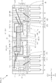
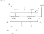
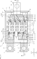
- FIG. 1 It is a perspective view which shows the semiconductor device which concerns on 1st Embodiment. It is a main part perspective view which shows the semiconductor device which concerns on 1st Embodiment. It is a top view which shows the semiconductor device which concerns on 1st Embodiment. It is a figure which showed the sealing resin by an imaginary line in the plan view of FIG. It is a partially enlarged plan view which enlarged a part of FIG. It is a front view which shows the semiconductor device which concerns on 1st Embodiment. It is a bottom view which shows the semiconductor device which concerns on 1st Embodiment. It is a left side view which shows the semiconductor device which concerns on 1st Embodiment.
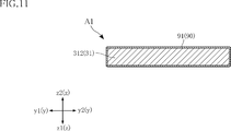
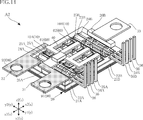
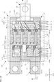
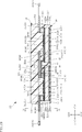
- FIG. 5 is a cross-sectional view taken along the line XX of FIG. It is sectional drawing which follows the XI-XI line of FIG. It is sectional drawing which shows the 1st modification of the semiconductor device which concerns on 1st Embodiment. It is sectional drawing which shows the 2nd modification of the semiconductor device which concerns on 1st Embodiment. It is a main part perspective view which shows the semiconductor device which concerns on 2nd Embodiment. It is a top view which shows the semiconductor device which concerns on 2nd Embodiment. It is sectional drawing which follows the XVI-XVI line of FIG.
- the semiconductor device A1 of the first embodiment includes a plurality of semiconductor elements 10, a support substrate 20, a plurality of leads, a plurality of intermediate leads 40, a plurality of wire members 50, a plurality of conductive blocks 60, a sealing resin 70, a capacitor 81, and the like.
- a coating layer 90 is provided.
- the plurality of leads include a first power lead 31, a second power lead 32, a third power lead 33, a pair of gate leads 34A and 34B, a pair of driver source leads 35A and 35B, and a plurality of dummy leads 36.
- the plurality of conductive blocks 60 include a plurality of first blocks 61 and a plurality of second blocks 62.
- FIG. 1 is a perspective view showing the semiconductor device A1.
- FIG. 2 is a perspective view of FIG. 1 in which the sealing resin 70 is omitted. In FIG. 2, a plurality of wire members 50 are omitted.
- FIG. 3 is a plan view showing the semiconductor device A1.
- FIG. 4 is a view showing the sealing resin 70 as an imaginary line (dashed-dotted line) in the plan view of FIG.
- FIG. 5 is a partially enlarged view of a part of FIG. 4.
- FIG. 6 is a front view showing the semiconductor device A1.
- FIG. 7 is a bottom view showing the semiconductor device A1.
- FIG. 8 is a left side view showing the semiconductor device A1.
- FIG. 9 is a right side view showing the semiconductor device A1.
- FIG. 1 is a perspective view showing the semiconductor device A1.
- FIG. 2 is a perspective view of FIG. 1 in which the sealing resin 70 is omitted.
- a plurality of wire members 50 are omitted.
- FIG. 3 is
- FIGS. 10 to 8 are cross-sectional views taken along the line XX of FIG.
- FIG. 11 is a cross-sectional view taken along the line XI-XI of FIG.
- a plurality of discrete points are drawn on the covering layer 90 for convenience of understanding.
- the z direction corresponds to the thickness direction of the semiconductor device A1.
- the x direction corresponds to the left-right direction in the plan view (see FIGS. 3 and 4) of the semiconductor device A1.
- the y direction corresponds to the vertical direction in the plan view (see FIGS. 3 and 4) of the semiconductor device A1. If necessary, one in the x direction is set to the x1 direction, and the other in the x direction is set to the x2 direction. Similarly, one in the y direction is the y1 direction, the other in the y direction is the y2 direction, one in the z direction is the z1 direction, and the other in the z direction is the z2 direction.
- Each of the plurality of semiconductor elements 10 has a function of switching the main circuit current, and the specific configuration thereof is not particularly limited.
- Specific examples of the semiconductor device 10 include SiC (silicon carbide) MOSET, SiC IGBT, Si MOSFET, Si IGBT (Insulated Gate Bipolar Transistor) and GaN (gallium nitride) HEMT (High Electron Mobility Transistor).
- Each semiconductor element 10 has a rectangular shape when viewed in the z direction (also referred to as "planar view”), but the present disclosure is not limited to this.
- Each of the plurality of semiconductor elements 10 has an element main surface 101 and an element back surface 102, as shown in FIGS. 5 and 10.
- the element main surface 101 and the element back surface 102 are separated from each other in the z direction and face opposite to each other.
- the element main surface 101 faces the z2 direction
- the element back surface 102 faces the z1 direction.
- Each of the plurality of semiconductor elements 10 has a main surface electrode 11, a back surface electrode 12, and an insulating film 13 as shown in FIGS. 5 and 10.
- the main surface electrode 11 is provided on the element main surface 101 as shown in FIG. As shown in FIG. 5, the main surface electrode 11 includes a source electrode 111, a gate electrode 112, and a driver source electrode 113.
- the source electrode 111 is an electrode through which a source current flows.
- a gate voltage for driving each semiconductor element 10 is applied to the gate electrode 112.
- the driver source electrode 113 is an electrode that serves as a reference potential for the gate voltage.
- the source electrode 111 is larger than the gate electrode 112 and the driver source electrode 113.
- the gate electrode 112 and the driver source electrode 113 have substantially the same size.
- the source electrode 111 is composed of one region, but may be divided into a plurality of regions.
- the back surface electrode 12 is provided on the back surface 102 of the element.
- the back surface electrode 12 is formed over the entire back surface 102 of the element.
- the back surface electrode 12 is an electrode through which a drain current flows, and is also referred to as a drain electrode 12 in the following description.
- the insulating film 13 is provided on the element main surface 101.
- the insulating film 13 has an electrical insulating property.
- the insulating film 13 surrounds the main surface electrode 11 in a plan view.
- the insulating film 13 insulates the source electrode 111 and the gate electrode 112.
- a SiO 2 (silicon dioxide) layer, a Si 3 N 4 (silicon nitride) layer, and a polybenzoxazole layer are laminated in this order on the element main surface 101, and the polybenzo The oxazole layer is the surface layer.
- a polyimide layer may be used instead of the polybenzoxazole layer.
- the configuration of the insulating film 13 is not limited to that described above.
- the plurality of semiconductor elements 10 include a plurality of first semiconductor elements 10A and a plurality of second semiconductor elements 10B.
- the semiconductor device A1 constitutes a half-bridge type switching circuit.
- the plurality of first semiconductor elements 10A form an upper arm circuit in this switching circuit
- the plurality of second semiconductor elements 10B form a lower arm circuit in this switching circuit.
- the semiconductor device A1 includes four first semiconductor elements 10A and four second semiconductor elements 10B.
- the number of semiconductor elements 10 is not limited to this configuration, and can be freely set according to the performance required for the semiconductor device A1.
- Each of the plurality of first semiconductor elements 10A is mounted on the support substrate 20 (conductive substrate 22A) as shown in FIGS. 2, 4, 5, and 10.
- the plurality of first semiconductor elements 10A are arranged in the y direction and are separated from each other.
- the element back surface 102 faces the conductive substrate 22A.
- Each first semiconductor element 10A is conductively bonded to the support substrate 20 (conductive substrate 22A) via, for example, a conductive element bonding material (not shown). Examples of the element bonding material include solder, sintered silver, silver paste and the like.
- Each of the plurality of second semiconductor elements 10B is mounted on the support substrate 20 (conductive substrate 22B) as shown in FIGS. 2, 4, 5, and 10.
- the plurality of second semiconductor elements 10B are arranged in the y direction and are separated from each other.
- the element back surface 102 faces the conductive substrate 22B.
- Each second semiconductor element 10B is conductively bonded to the support substrate 20 (conductive substrate 22B) via, for example, a conductive element bonding material (not shown).
- the plurality of first semiconductor elements 10A and the plurality of second semiconductor elements 10B overlap each other when viewed in the x direction. Instead, the plurality of first semiconductor elements 10A and the plurality of second semiconductor elements 10B do not have to overlap when viewed in the x direction.
- the support substrate 20 is a support member that supports a plurality of semiconductor elements 10.
- the support substrate 20 includes an insulating substrate 21, two conductive substrates 22A and 22B, a pair of insulating layers 23A and 23B, a pair of gate layers 24A and 24B, a pair of driver source layers 25A and 25B, and a first spacer 26A and a second spacer. It is provided with a spacer 26B.
- the insulating substrate 21 is a plate-shaped member having electrical insulation.
- the insulating substrate 21 supports two conductive substrates 22A and 22B.
- the insulating substrate 21 is composed of two insulating substrates 21A and 21B, each of which has a flat plate shape.
- the configuration of the insulating substrate 21 is not limited to that described above, and may be, for example, a single flat plate without being divided into the two insulating substrates 21A and 21B.
- the constituent materials of the insulating substrates 21A and 21B are, for example, ceramics having excellent thermal conductivity. Examples of such ceramics include AlN (aluminum nitride), SiN (silicon nitride), and Al 2 O 3 (aluminum oxide).
- the insulating substrates 21A and 21B each have a rectangular shape in a plan view.
- the insulating substrate 21A supports the conductive substrate 22A, and the insulating substrate 21B supports the conductive substrate 22B.
- the insulating substrates 21A and 21B are separated from each other. In the present embodiment, the insulating substrate 21A and the insulating substrate 21B are separated from each other in the x direction and arranged side by side as shown in FIGS. 2, 4 and 10.
- the insulating substrate 21A has a main surface 211A and a back surface 212A.
- the main surface 211A and the back surface 212A are separated from each other in the z direction and face opposite to each other.
- the main surface 211A faces the z2 direction, and the back surface 212A faces the z1 direction.
- the main surface 211A faces the conductive substrate 22A, and the back surface 212A is exposed from the sealing resin 70.
- another conductive substrate may be bonded to the back surface 212A of the insulating substrate 21A. In this case, the back surface of the conductive substrate is exposed from the sealing resin 70.
- the insulating substrate 21B has a main surface 211B and a back surface 212B.
- the main surface 211B and the back surface 212B are separated from each other in the z direction and face opposite to each other.
- the main surface 211B faces the z2 direction, and the back surface 212B faces the z1 direction.
- the main surface 211B faces the conductive substrate 22B, and the back surface 212B is exposed from the sealing resin 70.
- another conductive substrate may be bonded to the back surface 212B of the insulating substrate 21B. In this case, the back surface of the conductive substrate is exposed from the sealing resin 70.
- the conductive substrates 22A and 22B are plate-shaped members having conductivity, respectively.
- each of the conductive substrates 22A and 22B is a composite substrate including a graphite substrate 220 m and a copper film 220 n formed on both sides of the graphite substrate 220 m in the z direction.
- the constituent materials of the conductive substrates 22A and 22B are not limited to this, and may be Cu or a Cu alloy.
- the surfaces of the conductive substrates 22A and 22B may be covered with silver plating.
- the conductive substrates 22A and 22B include a plurality of leads (first power lead 31, second power lead 32, third power lead 33, a pair of gate leads 34A and 34B, a pair of driver source leads 35A and 35B, and a plurality of dummies. Together with the lead 36), it constitutes a conduction path to the plurality of semiconductor elements 10.
- the conductive substrates 22A and 22B are separated from each other. As shown in FIGS. 4 and 10, the conductive substrate 22A and the conductive substrate 22B are separated from each other in the x direction and are arranged side by side. As shown in FIG. 4, the conductive substrates 22A and 22B have a rectangular shape in a plan view.
- the conductive substrates 22A and 22B have dimensions in the z direction of about 1.0 to 3.5 mm.
- the z-direction dimension of the graphite substrate 220 m is about 0.5 to 2.5 mm
- each z-direction dimension of the pair of copper films 220n is about 0.25 to 0.5 mm.
- These dimensions in the z direction are not limited to those described above.
- the upper copper film 220n in FIG. 10 of the conductive substrate 22A is an example of the “first metal layer”, and the upper copper film 220n in FIG. 10 of the conductive substrate 22B is the “second metal layer”. Is an example.
- the material constituting the upper copper film 220n in the drawing of the conductive substrate 22A in FIG. 10 and the upper copper film 220n in the drawing of the conductive substrate 22B in FIG. 10 is an example of the “first material”.
- the conductive substrate 22A is bonded to the insulating substrate 21A via the substrate bonding material 220A.
- the substrate bonding material 220A may be, for example, a conductive bonding material such as silver paste, solder, or a sintered metal, or may be an insulating bonding material.
- the conductive substrate 22A is located in the x1 direction with respect to the conductive substrate 22B. All of the conductive substrate 22A overlaps the conductive substrate 22B when viewed in the x direction.
- the conductive substrate 22A has a main surface 221A and a back surface 222A.
- the main surface 221A and the back surface 222A are separated from each other in the z direction and face opposite to each other.
- the main surface 221A faces the z2 direction, and the back surface 222A faces the z1 direction.
- a plurality of first semiconductor elements 10A are mounted on the main surface 221A.
- the insulating layer 23A is joined to the main surface 221A.
- the conductive substrate 22B is bonded to the insulating substrate 21B via the substrate bonding material 220B.
- the substrate bonding material 220B may be, for example, a conductive bonding material such as silver paste, solder, or a sintered metal, or may be an insulating bonding material.
- the conductive substrate 22B has a main surface 221B and a back surface 222B.
- the main surface 221B and the back surface 222B are separated from each other in the z direction and face opposite to each other.
- the main surface 221B faces the z2 direction
- the back surface 222B faces the z1 direction.
- a plurality of second semiconductor elements 10B are mounted on the main surface 221B.
- the insulating layer 23B and one end of the plurality of intermediate leads 40 are joined to the main surface 221B, respectively.
- the pair of insulating layers 23A and 23B have electrical insulating properties, and the constituent material thereof is, for example, glass epoxy resin or ceramics. As shown in FIG. 4, each of the pair of insulating layers 23A and 23B has a strip shape extending in the y direction. As shown in FIGS. 4 and 10, the insulating layer 23A is joined to the main surface 221A of the conductive substrate 22A. The insulating layer 23A is located in the x1 direction with respect to the plurality of first semiconductor elements 10A. Instead, the insulating layer 23A may be arranged on the x2 direction side of the plurality of first semiconductor elements 10A. As shown in FIGS.
- the insulating layer 23B is joined to the main surface 221B of the conductive substrate 22B.
- the insulating layer 23B is located in the x2 direction with respect to the plurality of second semiconductor elements 10B.
- the insulating layer 23B may be arranged on the x1 direction side with respect to the plurality of second semiconductor elements 10B.
- the pair of gate layers 24A and 24B have conductivity, and the constituent material thereof is, for example, Cu or a Cu alloy. As shown in FIG. 4 and the like, the pair of gate layers 24A and 24B include a band-shaped portion extending in the y direction and a hook-shaped portion protruding from the band-shaped portion. The shapes of the pair of gate layers 24A and 24B are not limited to those shown in FIG. 4, and may be composed of, for example, no hook-shaped portion and only a strip-shaped portion.
- the gate layer 24A is arranged on the insulating layer 23A as shown in FIGS. 4 and 10. The gate layer 24A conducts to the gate electrode 112 of each first semiconductor element 10A via the wire member 50 (gate wire 51 described later).
- the gate layer 24B is arranged on the insulating layer 23B as shown in FIGS. 4 and 10. The gate layer 24B conducts to the gate electrode 112 of each second semiconductor element 10B via the wire member 50 (gate wire 51 described later).
- the pair of driver source layers 25A and 25B have conductivity, and the constituent material thereof is, for example, Cu or a Cu alloy. As shown in FIG. 4, the pair of driver source layers 25A and 25B include a band-shaped portion extending in the y direction and a hook-shaped portion protruding from the band-shaped portion. The shapes of the pair of driver source layers 25A and 25B are not limited to those shown in FIG. 4, and may be composed of, for example, no hook-shaped portion and only a strip-shaped portion. As shown in FIGS. 4 and 10, the driver source layer 25A is arranged on the insulating layer 23A together with the gate layer 24A.
- the driver source layer 25A is located on the insulating layer 23A next to the gate layer 24A and is separated from the gate layer 24A in a plan view.
- the driver source layer 25A is arranged closer to the plurality of first semiconductor elements 10A than the gate layer 24A in the x direction. Therefore, the driver source layer 25A is located on the x2 direction side of the gate layer 24A.
- the arrangement of the gate layer 24A and the driver source layer 25A in the x direction may be the opposite of the above.
- the driver source layer 25A conducts to the driver source electrode 113 of each first semiconductor element 10A via the wire member 50 (driver source wire 52). As shown in FIGS.
- the driver source layer 25B is arranged on the insulating layer 23B together with the gate layer 24B.
- the driver source layer 25B is located on the insulating layer 23B next to the gate layer 24B and is separated from the gate layer 24B in a plan view.
- the driver source layer 25B is arranged closer to the plurality of second semiconductor elements 10B than the gate layer 24B. Therefore, the driver source layer 25B is located on the x1 direction side of the gate layer 24B.
- the arrangement of the gate layer 24B and the driver source layer 25B in the x direction may be the opposite of the above.
- the driver source layer 25B conducts to the driver source electrode 113 of each second semiconductor element 10B via the wire member 50 (driver source wire 52).
- the first spacer 26A and the second spacer 26B have conductivity, and the constituent material thereof is, for example, Cu or a Cu alloy.
- the constituent materials of the first spacer 26A and the second spacer 26B are not limited to those described above, and may be, for example, a composite material of CuMo (Cu molybdenum), a composite material of CIC (Copper-Inver-Copper), or the like. good.
- the constituent materials of the first spacer 26A and the second spacer 26B may be different from each other.
- the first spacer 26A and the second spacer 26B are examples of the "conducting member", and the materials constituting the first spacer 26A and the second spacer 26B are examples of the "first material”.
- the first spacer 26A is interposed between the conductive substrate 22A and the first power lead 31.
- the first spacer 26A has a rectangular shape extending in the y direction in a plan view.
- the first spacer 26A is conductively bonded to the conductive substrate 22A.
- the first spacer 26A is located near the edge of the conductive substrate 22A in the x1 direction in a plan view.
- the first spacer 26A is provided so that the first power lead 31 is positioned substantially the same as the second power lead 32 in the z direction.
- the first spacer 26A may be absent and the first power lead 31 may be directly bonded to the conductive substrate 22A.
- the shape of the first spacer 26A is not particularly limited.
- the second spacer 26B is interposed between the conductive substrate 22B and the third power lead 33.
- the second spacer 26B has a rectangular shape extending in the y direction in a plan view.
- the second spacer 26B is conductively bonded to the conductive substrate 22B.
- the second spacer 26B is located near the edge of the conductive substrate 22B in the x2 direction in a plan view.
- the second spacer 26B is provided so that the third power lead 33 is positioned substantially the same as the second power lead 32 in the z direction.
- the third power lead 33 may be directly bonded to the conductive substrate 22B without the second spacer 26B.
- the shape of the second spacer 26B is not particularly limited.
- Each of the plurality of leads (first power lead 31, second power lead 32, third power lead 33, pair of gate leads 34A, 34B, pair of driver source leads 35A, 35B, and a plurality of dummy leads 36) is sealed. It includes a portion located inside the stop resin 70 and a portion located outside the sealing resin 70. That is, each lead includes a portion covered with the sealing resin 70 and a portion exposed from the sealing resin 70. Each lead is used when mounting the semiconductor device A1 on a circuit board of an electronic device or the like.
- the first power lead 31 and the second power lead 32 are metal plates, respectively.
- the constituent material of the metal plate is Cu or a Cu alloy.
- the constituent materials of the first power lead 31 and the second power lead 32 are not limited to this, and may be, for example, aluminum.
- both the first power lead 31 and the second power lead 32 have a dimension of about 0.8 mm in the z direction, but the present disclosure is not limited to this.
- Both the first power lead 31 and the second power lead 32 are located closer to the x1 direction in the semiconductor device A1 as shown in FIGS. 1 to 4 and 7. For example, a power supply voltage is applied between the first power lead 31 and the second power lead 32.
- the first power lead 31 is a positive electrode (P terminal), and the second power lead 32 is a negative electrode (N terminal).
- the first power lead 31 and the second power lead 32 are separated from each other.
- the second power lead 32 is separated from the conductive substrate 22A.
- the first power lead 31 and the second power lead 32 are examples of the "conducting member", and the materials constituting the first power lead 31 and the second power lead 32 are examples of the "first material”.
- the first power lead 31 has a pad portion 311 and a terminal portion 312.
- the pad portion 311 is a portion of the first power lead 31 covered with the sealing resin 70.
- the pad portion 311 conducts to the conductive substrate 22A via the first spacer 26A.
- the pad portion 311 is conductively bonded to the first spacer 26A.
- the method of conductive bonding is not limited at all, and may be, for example, laser bonding, bonding with a conductive bonding material, or the like.
- the terminal portion 312 is a portion of the first power lead 31 exposed from the sealing resin 70. As shown in FIGS. 3, 4, 6, 7, and 10, the terminal portion 312 extends from the sealing resin 70 in the x1 direction.
- the second power lead 32 has a pad portion 321 and a terminal portion 322.
- the pad portion 321 is a portion of the second power lead 32 covered with the sealing resin 70.
- the pad portion 321 includes a connecting portion 321a, a plurality of extending portions 321b, and a connecting portion 321c.
- the connecting portion 321a has a strip shape extending in the y direction.
- the connecting portion 321a connects a plurality of extending portions 321b.
- Each of the plurality of extending portions 321b has a strip shape extending from the connecting portion 321a in the x2 direction.
- each extending portion 321b extends from the connecting portion 321a in the x direction until it overlaps with each second semiconductor element 10B in a plan view.
- Each extending portion 321b extends from the conductive substrate 22A across the conductive substrate 22B in a plan view.
- the tip of each extension portion 321b overlaps the second block 62 in a plan view.
- the plurality of extending portions 321b are arranged in the y direction and separated from each other in a plan view.
- Each extending portion 321b conducts to the source electrode 111 (source electrode) of the second semiconductor element 10B via the plurality of conductive blocks 60.
- each extension portion 321b has its tip portion conductively joined to the second block 62.
- the method of conductive bonding is not limited at all, and may be, for example, laser bonding, bonding with a conductive bonding material, or the like.
- the connecting portion 321c is a portion that connects the connecting portion 321a and the terminal portion 322.
- the connecting portion 321c extends in the x1 direction from the end edge of the connecting portion 321a on the y2 direction side and the x1 direction side in the plan view.
- the terminal portion 322 is a portion of the second power lead 32 exposed from the sealing resin 70. As shown in FIGS. 1, 3, 4, and 7, the terminal portion 322 extends from the sealing resin 70 in the x1 direction.
- the terminal portion 322 has a rectangular shape in a plan view. As shown in FIGS. 3, 4, and 7, the terminal portion 322 is located on the y2 direction side of the terminal portion 312 of the first power lead 31 in a plan view.
- the shape of the terminal portion 322 is the same as the shape of the terminal portion 312, but the present disclosure is not limited thereto.
- the third power lead 33 is a metal plate.
- the constituent material of the metal plate is, for example, Cu or a Cu alloy.
- the constituent material of the third power lead 33 is not limited to this, and may be, for example, aluminum. As shown in FIGS. 1 to 4, 6, 7, and 10, the third power lead 33 is located closer to the x2 direction in the semiconductor device A1.
- the AC power (voltage) converted into power by the plurality of semiconductor elements 10 is output from the third power lead 33.
- the third power lead 33 includes a pad portion 331 and a terminal portion 332.
- the pad portion 331 is a portion of the third power lead 33 covered with the sealing resin 70.
- the pad portion 331 conducts to the conductive substrate 22B via the second spacer 26B. As shown in FIGS. 2, 4 and 10, the pad portion 331 is conductively bonded to the second spacer 26B.
- the method of conductive bonding is not limited at all, and may be, for example, laser bonding, bonding with a conductive bonding material, or the like.
- the terminal portion 332 is a portion of the third power lead 33 exposed from the sealing resin 70. As shown in FIGS. 3, 4, 6, 7, and 10, the terminal portion 332 extends from the sealing resin 70 in the x2 direction.
- the pair of gate leads 34A and 34B are located next to the respective conductive substrates 22A and 22B in the y direction.
- a gate voltage for driving a plurality of first semiconductor elements 10A is applied to the gate lead 34A.
- a gate voltage for driving a plurality of second semiconductor elements 10B is applied to the gate lead 34B.
- Both the pair of gate leads 34A and 34B have a pad portion 341 and a terminal portion 342 as shown in FIG.
- the pad portion 341 is covered with the sealing resin 70.
- the gate leads 34A and 34B are supported by the sealing resin 70.
- the terminal portion 342 is connected to the pad portion 341 and is exposed from the sealing resin 70.
- the terminal portion 342 has an L shape when viewed in the x direction. In the present embodiment, the terminal portion 342 protrudes from the surface (resin side surface 733) of the sealing resin 70 facing the y1 direction.
- the pair of driver source leads 35A and 35B are located next to the pair of gate leads 34A and 34B in the x direction.
- the driver source lead 35A is a lead that serves as a reference potential of a gate voltage for driving a plurality of first semiconductor elements 10A.
- the driver source lead 35B is a lead that serves as a reference potential for the gate voltage for driving the plurality of second semiconductor elements 10B.
- Both the pair of driver source leads 35A and 35B have a pad portion 351 and a terminal portion 352 as shown in FIG.
- the pad portion 351 is covered with the sealing resin 70.
- the driver source leads 35A and 35B are supported by the sealing resin 70.
- the terminal portion 352 is connected to the pad portion 351 and is exposed from the sealing resin 70.
- the terminal portion 352 has an L shape when viewed in the x direction. In the present embodiment, the terminal portion 352 protrudes from the surface (resin side surface 733) of the sealing resin 70 facing the y1 direction.
- the plurality of dummy leads 36 are located on the opposite sides of the pair of driver source leads 35A and 35B with respect to the pair of gate leads 34A and 34B in the x direction.
- the number of dummy leads 36 is four.
- the two dummy leads 36 are located on one side (x2 direction) in the x direction.
- the remaining two dummy leads 36 are located on the other side (x1 direction) in the x direction.
- the plurality of dummy leads 36 are not limited to the above-described configuration.
- the configuration may not include a plurality of dummy leads 36.
- Each of the plurality of dummy leads 36 has a pad portion 361 and a terminal portion 362 as shown in FIG.
- the pad portion 361 is covered with the sealing resin 70.
- the plurality of dummy leads 36 are supported by the sealing resin 70.
- the terminal portion 362 is connected to the pad portion 361 and is exposed from the sealing resin 70.
- the terminal portion 362 has an L shape when viewed in the x direction. In the present embodiment, the terminal portion 362 protrudes from the surface (resin side surface 733) of the sealing resin 70 facing the y1 direction.
- the gate leads 34A and 34B, the driver source leads 35A and 35B, and the dummy leads 36 have substantially the same shape. Then, as shown in FIGS. 1 to 7, these are arranged along the x direction.
- each lead first power lead 31, second power lead 32, third power lead 33, pair of gate leads 34A, 34B, pair of driver source leads 35A, 35B, and a plurality of dummy leads 36
- Both are formed from the same lead frame.
- the plurality of intermediate leads 40 connect each of the first semiconductor elements 10A and the conductive substrate 22B.
- the constituent material of each intermediate lead 40 is, for example, Cu or a Cu alloy.
- the constituent material of each intermediate lead 40 is not limited to this, and may be a clad material such as CIC, aluminum, or the like.
- Each intermediate lead 40 is a flat plate-shaped connecting member. As shown in FIG. 4, each intermediate lead 40 has a rectangular shape extending in the x direction in a plan view. Each intermediate lead 40 overlaps each extension portion 321b of the second power lead 32 in a plan view.
- the intermediate lead 40 is an example of a “conducting member”, and the material constituting the intermediate lead 40 is an example of a “first material”.
- each intermediate lead 40 includes a first joint portion 41, a second joint portion 42, and a connecting portion 43.
- the first joint portion 41 is a portion joined to the first block 61.
- the first joint portion 41 and the first block 61 are conductively joined.
- the method of conductive bonding is not particularly limited, and may be, for example, laser bonding, bonding with a conductive bonding material, or the like.
- the second joint portion 42 is a portion joined to the conductive substrate 22B.
- the second joint portion 42 and the conductive substrate 22B are conductively joined.
- the method of conductive bonding is not particularly limited, and may be, for example, laser bonding, bonding with a conductive bonding material, or the like.
- the contact portion 43 is a portion connected to the first joint portion 41 and the second joint portion 42.
- the dimensions of the connecting portion 43 in the z direction are the same as those of the first joint portion 41 and the second joint portion 42.
- the connecting portion 43 is partially bent in the z direction. Since the connecting portion 43 is bent, the first joint portion 41 and the second joint portion 42 having different positions in the z direction are connected.
- Each of the plurality of wire members 50 is a wire (bonding wire).
- Each wire member 50 has conductivity, and the constituent material thereof is, for example, aluminum, gold, or Cu.
- the plurality of wire members 50 include a plurality of gate wires 51, a plurality of driver source wires 52, a pair of first connection wires 53, and a pair of second connection wires 54. Includes.
- each of the plurality of gate wires 51 has one end (first end) joined to the gate electrode 112 of each semiconductor element 10, and the other end (second end) is a pair of gate layers 24A. It is joined to any of 24B.
- the plurality of gate wires 51 include one that conducts the gate electrode 112 of each first semiconductor element 10A and the gate layer 24A, and one that conducts the gate electrode 112 of each second semiconductor element 10B and the gate layer 24B. be.
- each of the plurality of driver source wires 52 is bonded to the driver source electrode 113 of each semiconductor element 10, and the other end is bonded to either of the pair of driver source layers 25A and 25B.
- the plurality of driver source wires 52 are provided with one that conducts the driver source electrode 113 of each first semiconductor element 10A and the driver source layer 25A, and the driver source electrode 113 and the driver source layer 25B of each second semiconductor element 10B. Some are conductive.
- one of the pair of first connecting wires 53 connects the gate layer 24A and the gate lead 34A, and the other connects the gate layer 24B and the gate lead 34B.
- One end of the first connecting wire 53 is joined to the gate layer 24A, and the other end is joined to the pad portion 341 of the gate lead 34A.
- One end of the other first connecting wire 53 is joined to the gate layer 24B, and the other end is joined to the pad portion 341 of the gate lead 34B.
- one of the pair of second connecting wires 54 connects the driver source layer 25A and the driver source lead 35A, and the other connects the driver source layer 25B and the driver source lead 35B.
- One end of the second connection wire 54 is joined to the driver source layer 25A, and the other end is joined to the pad portion 351 of the driver source lead 35A.
- One end of the other second connection wire 54 is joined to the driver source layer 25B, and the other end is joined to the pad portion 351 of the driver source lead 35B.
- the plurality of conductive blocks 60 have conductivity. Each of the plurality of conductive blocks 60 is bonded onto one corresponding semiconductor element 10. Each conductive block 60 has a z-direction dimension of about 0.1 to 2.0 mm, but the present disclosure is not limited to this.
- the plurality of conductive blocks 60 include a plurality of first blocks 61 and a plurality of second blocks 62.
- Each of the plurality of first blocks 61 is bonded to one of the plurality of first semiconductor elements 10A.
- Each first block 61 is conductively bonded to each first semiconductor element 10A by solder or the like.
- Each first block 61 faces the element main surface 101 of each first semiconductor element 10A.
- each first block 61 is a columnar body and has a rectangular shape in a plan view as shown in FIG.
- the plan view shape of each first block 61 is not limited to this, and may be circular, elliptical, or polygonal.
- the first block 61 is made of, for example, Cu or a Cu alloy.
- Each of the plurality of second blocks 62 is bonded to one of the plurality of second semiconductor elements 10B.
- Each second block 62 is conductively bonded to each second semiconductor element 10B by solder or the like.
- Each second block 62 faces the element main surface 101 of each second semiconductor element 10B.
- the z-direction dimension of each second block 62 is not particularly limited, but is, for example, about 1.83 mm in the present embodiment.
- each second block 62 is a columnar body and has a rectangular shape in a plan view, as shown in FIGS. 4 and 10.
- the plan view shape of each second block 62 is not limited to this, and may be circular, elliptical, or polygonal.
- the second block 62 is made of, for example, Cu or a Cu alloy.
- each first block 61 in the z direction is smaller than the dimension of each second block 62 in the z direction.
- the z-direction dimension of each second block 62 is about 1.83 mm as described above, so that the z-direction dimension of each first block 61 is smaller than this value.
- the capacitor 81 is a chip type having a first end and a second end, the first end is mounted on the pad portion 311 of the first power lead 31, and the second end is the connecting portion 321a of the second power lead 32. It is placed in.
- the bonding between the capacitor 81 and the power leads 31 and 32 can be performed by, for example, a conductive bonding material.
- the power supply voltage (input voltage) applied between the first power lead 31 and the second power lead 32 is stabilized. Can be achieved.
- the capacitor 81 may be referred to as a DC link capacitor. Unlike the present embodiment, the configuration may not include the capacitor 81.
- the sealing resin 70 includes a plurality of semiconductor elements 10, a part of the support substrate 20, and a plurality of leads (first power lead 31, second power lead 32, third power lead 33). , A pair of gate leads 34A, 34B, a pair of driver source leads 35A, 35B and a plurality of dummy leads 36), covering a plurality of intermediate leads 40, a plurality of wire members 50, and a plurality of conductive blocks 60. ..
- the constituent material of the sealing resin 70 is, for example, an epoxy resin.
- the sealing resin 70 has a resin main surface 71, a resin back surface 72, and a plurality of resin side surfaces 731 to 734.
- the resin main surface 71 and the resin back surface 72 are separated from each other in the z direction and face opposite to each other.
- the resin main surface 71 faces the z2 direction
- the resin back surface 72 faces the z1 direction.
- the resin back surface 72 has a frame shape surrounding the back surface 212A of the insulating substrate 21A and the back surface 212B of the insulating substrate 21B in a plan view.
- the back surfaces 212A and 212B are exposed from the resin back surface 72.
- each of the plurality of resin side surfaces 731 to 734 is connected to both the resin main surface 71 and the resin back surface 72, and is sandwiched between them in the z direction.
- the resin side surfaces 731 and 732 are separated in the x direction and face opposite to each other.
- the resin side surface 731 faces the x1 direction
- the resin side surface 732 faces the x2 direction.
- the resin side surfaces 733 and 734 are separated in the y direction and face opposite to each other.
- the resin side surface 733 faces the y1 direction
- the resin side surface 734 faces the y2 direction.
- the coating layer 90 is a layer that covers at least a part of the "conducting member" and is made of a second material.
- This second material meets at least one of the following three requirements. (1) The magnetic permeability is higher than that of the first material constituting the "conducting member”. (2) The electrical resistivity is higher than that of the first material. (3) The dielectric loss tangent is greater than 0 (greater than the dielectric loss tangent of an ideal dielectric). Regarding these, for example, it is assumed that the first material is Cu.
- examples of the second material having a higher magnetic permeability than the first material include magnetic metals such as Ni, Co, and Fe.
- the second material having a higher electrical resistivity than the first material examples include metals such as Ni, W, and Mo, conductive polymers, and transparent conductive films.
- a second material having a dielectric loss tangent larger than 0, for example, a dielectric can be mentioned.
- the magnetic permeability of the second material is higher than the magnetic permeability of the first material
- the relative magnetic permeability of the second material is preferably, for example, 10 or more.
- the electrical resistivity of the second material is made higher than the electrical resistivity of the first material
- the electrical resistivity of the second material is preferably, for example, twice or more the electrical resistivity of the first material.
- the dielectric loss tangent of the second material is preferably 0.01 or more.
- the thickness of the coating layer 90 is not particularly limited, and is, for example, 1 ⁇ m to 5 ⁇ m. When the coating layer 90 is made of metal, the coating layer 90 is formed by plating such as magnetic plating.
- the coating layer 90 may be a magnetic metal in which the magnetic permeability of the second material is higher than the magnetic permeability of the first material and the electrical resistivity of the second material is higher than the electrical resistivity of the first material.
- the coating layer 90 may have a structure in which the magnetic permeability of the second material is higher than the magnetic permeability of the first material and the dielectric loss tangent of the second material is larger than 0.
- the coating layer 90 may have a configuration in which the electrical resistivity of the second material is higher than the electrical resistivity of the first material and the dielectric loss tangent of the second material is larger than 0.
- the magnetic permeability of the second material is higher than the magnetic permeability of the first material
- the electrical resistivity of the second material is higher than the electrical resistivity of the first material
- the dielectric constant contact of the second material is The configuration may be larger than 0.
- the covering layer 90 has a first part 91 and a second part 92.
- the first part 91 covers at least a part of the first power lead 31. In the present embodiment, the first part 91 covers all of the first power lead 31.
- the first part 91 covers at least a part of the second power lead 32. In this embodiment, the second part 92 covers all of the second power lead 32. Similar to the first part 91, when the second power lead 32 functions as a path for the main circuit current, the entire circumference of the cross section of the second power lead 32 is covered by the second part 92.
- the coating layer 90 is provided on the conductive member that forms the path of the main circuit current in the semiconductor device A1. More specifically, the coating layer 90 is provided at a portion where the density of the alternating current increases due to the skin effect.
- the magnetic permeability of the second material constituting the coating layer 90 is higher than the magnetic permeability of the first material (Cu or the like) constituting the conductive member (first power lead 31, second power lead 32, etc.)
- the skin effect The effect of is more pronounced, and the AC resistance of the current path increases.
- the coating layer 90 does not unreasonably attenuate the low frequency component of the current. Further, since ringing can be suppressed, the snubber circuit provided in the semiconductor device A1 can be simplified, and the reliability of the semiconductor device A1 itself can be improved.
- the electrical resistivity of the second material constituting the coating layer 90 is higher than the electrical resistivity of the first material (Cu or the like) constituting the conductive member (first power lead 31, second power lead 32, etc.). Even when it is high, it is possible to attenuate the alternating current flowing through the coating layer 90 and suppress ringing. As mentioned above, the low frequency components of the current are not unduly attenuated by the coating layer 90.
- the dielectric loss tangent of the second material constituting the coating layer 90 is larger than 0 (larger than the dielectric loss tangent of the ideal dielectric)
- the energy of the alternating current flowing through the coating layer 90 can be consumed as a dielectric loss. It is possible and it is possible to suppress ringing.
- FIG. 12 shows a first modification of the semiconductor device A1.
- the configuration of the coating layer 90 is different from the above-described example.
- the first part 91 which is a part of the coating layer 90, as an example, in this modified example, in the cross section through which the main circuit current flows, the first part 91 covers the entire circumference of the cross section of the first power lead 31. It does not cover only a part of it. More specifically, the first part 91 covers only three sides (upper side and two side sides) of the rectangular cross section of the first power lead 31 and does not cover the remaining one side (bottom side) (that is, the bottom side). , The bottom is exposed from Part 1 91). The three sides (upper side and two side sides) are completely covered by the first part 91, respectively.
- FIG. 13 shows a second modification of the semiconductor device A1.
- the first part 91 which is a part of the coating layer 90, as an example
- the first part 91 is formed over the entire circumference of the cross section of the first power lead 31 in the cross section through which the main circuit current flows.
- both sides top, two sides, and bottom
- Part 1 91 in other words, partially covered by Part 1 91).
- the first portion 91 has a plurality of gap portions arranged apart from each other along the entire circumference of the rectangular cross section.
- the plurality of voids include one or more voids corresponding to each side of the cross section.
- first part 91 for example, a configuration in which a plurality of small holes and slits are formed can be formed.
- first part 91 can be configured as an aggregate of a plurality of small regions separated from each other.
- Ringing can also be suppressed by the semiconductor devices A11 and A12.
- the specific configuration of the coating layer 90 is not particularly limited. Even if the coating layer 90 covers a part of the conductive member (FIGS. 12 and 13), the effect of suppressing ringing can be expected depending on the position and size of the region where the coating layer 90 is provided. ..
- the configuration of the coating layer 90 is different from that of the coating layer 90 of the semiconductor device A1 described above.
- the first part 91 covers a part of the first power lead 31, and the second part 92 covers a part of the second power lead 32. More specifically, the first part 91 does not cover the portion of the first power lead 31 that constitutes the path between the first semiconductor element 10A and the capacitor 81. That is, the first part 91 covers the terminal part 312 of the first power lead 31, but does not cover the pad part 311.
- the second part 92 does not cover the portion of the second power lead 32 that constitutes the path between the second semiconductor element 10B and the capacitor 81. That is, the second portion 92 covers the terminal portion 322 of the second power lead 32 and the connecting portion 321c of the pad portion 321 while not covering the connecting portion 321a and the plurality of extending portions 321b.
- the resistance of the portion of the first power lead 31 and the second power lead 32 that constitutes the path through which only the charge / discharge current of the capacitor 81 flows is equivalent to the ESR of the capacitor 81. That is, since this path is a path through which a steep charge / discharge current flows to the capacitor 81, it is not preferable that the AC resistance is too high. In this respect, the fact that the first part 91 and the second part 92 do not cover each part of the first power lead 31 and the second power lead 32 as described above means that the capacitor 81 is steeply charged. Preferred for discharging.
- FIG 17 to 19 show the semiconductor device according to the third embodiment of the present disclosure.
- the configuration of the coating layer 90 is different from that of the coating layer 90 of the semiconductor devices A1 and A2 described above.
- the coating layer 90 includes a first part 91, a second part 92, a third part 93, a fourth part 94, a fifth part 95, and a sixth part 96.
- the first part 91 and the second part 92 have the same configuration as the first part 91 and the second part 92 in the semiconductor device A1.
- the third part 93 covers the copper film 220n of the conductive substrate 22A as the first metal layer.
- Part 4 94 covers the first spacer 26A.
- Part 5 95 covers the copper film 220n of the conductive substrate 22B as the second metal layer.
- Part 6 96 covers a plurality of intermediate leads 40.
- the third part 93 covers the portion of the copper film 220n excluding the joint surface with the graphite substrate 220m.
- Part 5 95 covers the portion of the copper film 220n excluding the joint surface with the graphite substrate 220m.
- Ringing can also be suppressed by the third embodiment. Further, as understood from the present embodiment, the location of the coating layer 90 can be appropriately changed according to the required degree of ringing suppression and the configuration of the semiconductor device.
- the semiconductor device A4 of the present embodiment shows the configurations of the first power lead 31 and the second power lead 32 are different from those of the above-described embodiment.
- the terminal portion 312 of the first power lead 31 and the terminal portion 322 of the second power lead 32 overlap each other when viewed along the z direction.
- the terminal portion 312 is covered by the first portion 91, and the terminal portion 322 is covered by the second portion 92.
- An insulator 89 is provided between the terminal portion 312 and the terminal portion 322. The insulator 89 is for insulating each other between the terminal portion 312 and the terminal portion 322 when an assumed voltage is applied.
- the second material constituting the coating layer 90 is made of a material having a dielectric loss tangent of at least 0 (larger than the dielectric loss tangent of the ideal dielectric), for example, a dielectric loss tangent of 0.01 or more.
- the coating layer 90 having such a configuration is adopted, the terminal portion 312 and the terminal portion 322 and the coating layer 90 and the insulator 89 interposed between them provide a portion having a capacitance, that is, electricity similar to a capacitor. A part having a specific structure is realized.
- Ringing can also be suppressed by the fourth embodiment.
- the capacitance composed of the terminal portion 312 and the terminal portion 322 and the coating layer 90 and the insulator 89 interposed between them is expected to exert a synergistic effect with the capacitor 81, and the first power lead.
- the effect of stabilizing the power supply voltage (input voltage) applied between the 31 and the second power lead 32 can be further enhanced.
- the semiconductor device according to the present disclosure is not limited to the above-described embodiments and modifications.
- the specific configuration of each part of the semiconductor device of the present disclosure can be freely redesigned.
- the semiconductor device includes the embodiments described in the following appendices.
- Appendix 1 With at least one semiconductor element having a switching function, A conductive member that serves as a path for a current switched by the semiconductor element and is made of a first material, A coating layer that covers at least a part of the conductive member and is made of a second material, Is equipped with The second material has the following three requirements: (A) Higher magnetic permeability than the first material, (B) Higher electrical resistivity than the first material, and (c) Dissipation factor greater than 0. A semiconductor device that meets at least one of the requirements. Appendix 2.
- the semiconductor device according to Appendix 1, wherein the second material is a magnetic conductor having a higher magnetic permeability than the first material and a higher electrical resistivity than the first material.
- Appendix 3. The semiconductor device according to Appendix 2, wherein the second material has a dielectric loss tangent larger than 0.
- Appendix 4. The semiconductor device according to Appendix 1, wherein the second material has a higher magnetic permeability than the first material and has a dielectric loss tangent larger than 0.
- Appendix 5 The semiconductor device according to Appendix 1, wherein the second material has a higher electrical resistivity than the first material and has a dielectric loss tangent larger than 0. Appendix 6.
- Appendix 7. The semiconductor device according to any one of Supplementary note 1 to 6, wherein the relative magnetic permeability of the second material is 10 or more.
- Appendix 8. The semiconductor device according to any one of Supplementary note 1 to 7, wherein the electrical resistivity of the second material is at least twice the electrical resistivity of the first material.
- Appendix 10. It further comprises a capacitor with first and second ends for electrical connection.
- the at least one semiconductor element is a plurality of semiconductor elements constituting a half bridge including at least one set of upper and lower arms.
- the plurality of semiconductor elements include a first semiconductor element included in the upper arm and a second semiconductor element included in the lower arm.
- the conductive member was connected to a first metal layer connected to the drain electrode of the first semiconductor element, a first power lead connected to the first metal layer, and a source electrode of the second semiconductor element. Including the second power lead, The first end of the capacitor is connected to the first power lead, and the second end of the capacitor is connected to the second power lead.
- the semiconductor device according to any one of Supplementary note 1 to 9, wherein the coating layer includes a first part that covers the first power lead and a second part that covers the second power lead. Appendix 11.
- the first power lead includes a portion forming a path between the first semiconductor element and the capacitor, and the portion of the first power lead is not covered by the first part, according to Appendix 10.
- the second power lead includes a portion forming a path between the second semiconductor element and the capacitor, and the portion of the second power lead is not covered by the second part, according to Appendix 10 or 11.
- Appendix 13 The semiconductor device according to any one of Appendix 10 to 12, wherein the coating layer includes a third part that covers the first metal layer.
- the conductive member includes a second metal layer connected to the drain electrode of the second semiconductor element and a third power lead connected to the second metal layer.
- Appendix 15. The semiconductor device according to Appendix 14, wherein the conductive member includes an intermediate lead connected to the source electrode of the first semiconductor element and the second metal layer, and the intermediate lead is not covered by the coating layer. .. Appendix 16.
- the conductive member includes a first spacer interposed between the first metal layer and the first power lead.
- Appendix 17. The semiconductor device according to any one of Appendix 10 to 16, wherein the conductive member includes a conductor interposed between the source electrode of the second semiconductor element and the second power lead.
- Appendix 18. The semiconductor device according to any one of Appendix 1 to 17, wherein the semiconductor element is any one of SiC MOSET, SiC IGBT, Si MOSFET, Si IGBT and GaN HEMT.
Landscapes
- Engineering & Computer Science (AREA)
- Power Engineering (AREA)
- Structures Or Materials For Encapsulating Or Coating Semiconductor Devices Or Solid State Devices (AREA)
- Inverter Devices (AREA)
- Recrystallisation Techniques (AREA)
- Hall/Mr Elements (AREA)
- Insulated Gate Type Field-Effect Transistor (AREA)
- Wire Bonding (AREA)
Abstract
Description
付記1.
スイッチング機能を有する少なくとも1つの半導体素子と、
前記半導体素子によってスイッチングされる電流の経路となり且つ第1素材からなる導通部材と、
前記導通部材の少なくとも一部を覆い且つ第2素材からなる被覆層と、
を備えており、
前記第2素材は、以下の3つの要件:
(a)前記第1素材よりも透磁率が高い、
(b)前記第1素材よりも電気抵抗率が高い、および
(c)誘電正接が0より大きい、
のうちの少なくとも1つの要件を満たす、半導体装置。
付記2.
前記第2素材は、前記第1素材よりも透磁率が高く且つ前記第1素材よりも電気抵抗率が高い磁性導電体である、付記1に記載の半導体装置。
付記3.
前記第2素材は、誘電正接が0より大きい、付記2に記載の半導体装置。
付記4.
前記第2素材は、前記第1素材よりも透磁率が高く且つ誘電正接が0より大きい、付記1に記載の半導体装置。
付記5.
前記第2素材は、前記第1素材よりも電気抵抗率が高く且つ誘電正接が0より大きい、付記1に記載の半導体装置。
付記6.
前記被覆層の厚さは、1μm~5μmである、付記1ないし5のいずれかに記載の半導体装置。
付記7.
前記第2素材の比透磁率は、10以上である、付記1ないし6のいずれかに記載の半導体装置。
付記8.
前記第2素材の電気抵抗率は、前記第1素材の電気抵抗率の2倍以上である、付記1ないし7のいずれかに記載の半導体装置。
付記9.
前記第2素材の誘電正接は、0.01以上である、付記1ないし8のいずれかに記載の半導体装置。
付記10.
電気接続用の第1端および第2端を有するコンデンサをさらに備えており、
前記少なくとも1つの半導体素子は、少なくとも1組の上下アームを含むハーフブリッジを構成する複数の半導体素子であり、
前記複数の半導体素子は、前記上アームに含まれる第1半導体素子と、前記下アームに含まれる第2半導体素子と、を含み、
前記導通部材は、前記第1半導体素子のドレイン電極に接続された第1金属層と、前記第1金属層に接続された第1パワーリードと、前記第2半導体素子のソース電極に接続された第2パワーリードと、を含み、
前記コンデンサの前記第1端は、前記第1パワーリードに接続され、前記コンデンサの前記第2端は、前記第2パワーリードに接続されており、
前記被覆層は、前記第1パワーリードを覆う第1部と、前記第2パワーリードを覆う第2部とを含む、付記1ないし9のいずれかに記載の半導体装置。
付記11.
前記第1パワーリードは、前記第1半導体素子と前記コンデンサとの経路を構成する部分を含み、前記第1パワーリードの当該部分は、前記第1部によって覆われていない、付記10に記載の半導体装置。
付記12.
前記第2パワーリードは、前記第2半導体素子と前記コンデンサとの経路を構成する部分を含み、前記第2パワーリードの当該部分は、前記第2部によって覆われていない、付記10または11に記載の半導体装置。
付記13.
前記被覆層は、前記第1金属層を覆う第3部を含む、付記10ないし12のいずれかに記載の半導体装置。
付記14.
前記導通部材は、前記第2半導体素子のドレイン電極に接続された第2金属層と、前記第2金属層に接続された第3パワーリードとを含み、
前記第2金属層および前記第3パワーリードは、前記被覆層によって覆われていない、付記10ないし13のいずれかに記載の半導体装置。
付記15.
前記導通部材は、前記第1半導体素子のソース電極と前記第2金属層とに接続された中間リードを含み、前記中間リードは、前記被覆層によって覆われていない、付記14に記載の半導体装置。
付記16.
前記導通部材は、前記第1金属層と前記第1パワーリードとの間に介在する第1スペーサを含み、
前記被覆層は、前記第1スペーサを覆う第4部を含む、付記10ないし15のいずれかに記載の半導体装置。
付記17.
前記導通部材は、前記第2半導体素子のソース電極と前記第2パワーリードとの間に介在する導体を含む、付記10ないし16のいずれかに記載の半導体装置。
付記18.
前記半導体素子は、SiC MOSET、SiC IGBT、Si MOSFET、Si IGBTおよびGaN HEMTのいずれかである、付記1ないし17のいずれかに記載の半導体装置。
10 :半導体素子
10A :第1半導体素子
10B :第2半導体素子
11 :主面電極
12 :ドレイン電極(裏面電極)
13 :絶縁膜
20 :支持基板
21,21A,21B:絶縁基板
22A,22B:導電性基板
23A,23B:絶縁層
24A,24B:ゲート層
25A,25B:ドライバソース層
26A :第1スペーサ
31 :第1パワーリード
32 :第2パワーリード
33 :第3パワーリード
34A,34B:ゲートリード
35A,35B:ドライバソースリード
36 :ダミーリード
40 :中間リード
41 :第1接合部
42 :第2接合部
43 :連絡部
50 :ワイヤ部材
51 :ゲートワイヤ
52 :ドライバソースワイヤ
53 :第1接続ワイヤ
54 :第2接続ワイヤ
60 :導電ブロック
61 :第1ブロック
62 :第2ブロック
70 :封止樹脂
71 :樹脂主面
72 :樹脂裏面
81 :コンデンサ
89 :絶縁体
90 :被覆層
91 :第1部
92 :第2部
93 :第3部
94 :第4部
95 :第5部
96 :第6部
101 :素子主面
102 :素子裏面
111 :ソース電極
112 :ゲート電極
113 :ドライバソース電極
211A,211B:主面
212A,212B:裏面
220A,220B:基板接合材
220m :グラファイト基板
220n :銅膜
221A,221B:主面
222A,222B:裏面
260A :スペーサ接合材
260B :スペーサ接合材
311,321,331,341,351,361 :パッド部
312,322,332,342,352,362 :端子部
321a :連結部
321b :延出部
321c :接続部
731,732,733,734:樹脂側面
Claims (18)
- スイッチング機能を有する少なくとも1つの半導体素子と、
前記半導体素子によってスイッチングされる電流の経路となり且つ第1素材からなる導通部材と、
前記導通部材の少なくとも一部を覆い且つ第2素材からなる被覆層と、
を備えており、
前記第2素材は、以下の3つの要件:
(a)前記第1素材よりも透磁率が高い、
(b)前記第1素材よりも電気抵抗率が高い、および
(c)誘電正接が0より大きい、
のうちの少なくとも1つの要件を満たす、半導体装置。 - 前記第2素材は、前記第1素材よりも透磁率が高く且つ前記第1素材よりも電気抵抗率が高い磁性導電体である、請求項1に記載の半導体装置。
- 前記第2素材は、誘電正接が0より大きい、請求項2に記載の半導体装置。
- 前記第2素材は、前記第1素材よりも透磁率が高く且つ誘電正接が0より大きい、請求項1に記載の半導体装置。
- 前記第2素材は、前記第1素材よりも電気抵抗率が高く且つ誘電正接が0より大きい、請求項1に記載の半導体装置。
- 前記被覆層の厚さは、1μm~5μmである、請求項1ないし5のいずれかに記載の半導体装置。
- 前記第2素材の比透磁率は、10以上である、請求項1ないし6のいずれかに記載の半導体装置。
- 前記第2素材の電気抵抗率は、前記第1素材の電気抵抗率の2倍以上である、請求項1ないし7のいずれかに記載の半導体装置。
- 前記第2素材の誘電正接は、0.01以上である、請求項1ないし8のいずれかに記載の半導体装置。
- 電気接続用の第1端および第2端を有するコンデンサをさらに備えており、
前記少なくとも1つの半導体素子は、少なくとも1組の上下アームを含むハーフブリッジを構成する複数の半導体素子であり、
前記複数の半導体素子は、前記上アームに含まれる第1半導体素子と、前記下アームに含まれる第2半導体素子と、を含み、
前記導通部材は、前記第1半導体素子のドレイン電極に接続された第1金属層と、前記第1金属層に接続された第1パワーリードと、前記第2半導体素子のソース電極に接続された第2パワーリードと、を含み、
前記コンデンサの前記第1端は、前記第1パワーリードに接続され、前記コンデンサの前記第2端は、前記第2パワーリードに接続されており、
前記被覆層は、前記第1パワーリードを覆う第1部と、前記第2パワーリードを覆う第2部とを含む、請求項1ないし9のいずれかに記載の半導体装置。 - 前記第1パワーリードは、前記第1半導体素子と前記コンデンサとの経路を構成する部分を含み、前記第1パワーリードの当該部分は、前記第1部によって覆われていない、請求項10に記載の半導体装置。
- 前記第2パワーリードは、前記第2半導体素子と前記コンデンサとの経路を構成する部分を含み、前記第2パワーリードの当該部分は、前記第2部によって覆われていない、請求項10または11に記載の半導体装置。
- 前記被覆層は、前記第1金属層を覆う第3部を含む、請求項10ないし12のいずれかに記載の半導体装置。
- 前記導通部材は、前記第2半導体素子のドレイン電極に接続された第2金属層と、前記第2金属層に接続された第3パワーリードとを含み、
前記第2金属層および前記第3パワーリードは、前記被覆層によって覆われていない、請求項10ないし13のいずれかに記載の半導体装置。 - 前記導通部材は、前記第1半導体素子のソース電極と前記第2金属層とに接続された中間リードを含み、前記中間リードは、前記被覆層によって覆われていない、請求項14に記載の半導体装置。
- 前記導通部材は、前記第1金属層と前記第1パワーリードとの間に介在する第1スペーサを含み、
前記被覆層は、前記第1スペーサを覆う第4部を含む、請求項10ないし15のいずれかに記載の半導体装置。 - 前記導通部材は、前記第2半導体素子のソース電極と前記第2パワーリードとの間に介在する導体を含む、請求項10ないし16のいずれかに記載の半導体装置。
- 前記半導体素子は、SiC MOSET、SiC IGBT、Si MOSFET、Si IGBTおよびGaN HEMTのいずれかである、請求項1ないし17のいずれかに記載の半導体装置。
Priority Applications (6)
| Application Number | Priority Date | Filing Date | Title |
|---|---|---|---|
| JP2022511851A JP7648602B2 (ja) | 2020-03-30 | 2021-03-17 | 半導体装置 |
| US17/914,713 US20230146758A1 (en) | 2020-03-30 | 2021-03-17 | Semiconductor device |
| DE112021002114.1T DE112021002114B4 (de) | 2020-03-30 | 2021-03-17 | Halbleiterbauteil |
| CN202511728129.9A CN121532044A (zh) | 2020-03-30 | 2021-03-17 | 半导体装置 |
| CN202180024426.9A CN115335988B (zh) | 2020-03-30 | 2021-03-17 | 半导体装置 |
| JP2025035926A JP2025085005A (ja) | 2020-03-30 | 2025-03-06 | 半導体装置 |
Applications Claiming Priority (2)
| Application Number | Priority Date | Filing Date | Title |
|---|---|---|---|
| JP2020060295 | 2020-03-30 | ||
| JP2020-060295 | 2020-03-30 |
Publications (1)
| Publication Number | Publication Date |
|---|---|
| WO2021200166A1 true WO2021200166A1 (ja) | 2021-10-07 |
Family
ID=77929262
Family Applications (1)
| Application Number | Title | Priority Date | Filing Date |
|---|---|---|---|
| PCT/JP2021/010866 Ceased WO2021200166A1 (ja) | 2020-03-30 | 2021-03-17 | 半導体装置 |
Country Status (5)
| Country | Link |
|---|---|
| US (1) | US20230146758A1 (ja) |
| JP (2) | JP7648602B2 (ja) |
| CN (2) | CN121532044A (ja) |
| DE (1) | DE112021002114B4 (ja) |
| WO (1) | WO2021200166A1 (ja) |
Cited By (3)
| Publication number | Priority date | Publication date | Assignee | Title |
|---|---|---|---|---|
| KR20240042103A (ko) * | 2021-11-26 | 2024-04-01 | 비와이디 컴퍼니 리미티드 | 파워 모듈 및 전기 장비 |
| EP4345898A3 (de) * | 2022-09-28 | 2024-04-17 | ZF Friedrichshafen AG | Halbbrücken-leistungsvorrichtung und halbbrücken-leistungsmodul |
| WO2025224977A1 (ja) * | 2024-04-26 | 2025-10-30 | 三菱電機株式会社 | 半導体装置、インバータ装置および半導体装置の製造方法 |
Families Citing this family (3)
| Publication number | Priority date | Publication date | Assignee | Title |
|---|---|---|---|---|
| JP7570298B2 (ja) * | 2021-07-26 | 2024-10-21 | 三菱電機株式会社 | 半導体装置 |
| NL2038368B1 (en) * | 2024-07-31 | 2026-02-17 | Nexperia BV | A semiconductor package, a half bridge clip, and a method for manufacturing said semiconductor package. |
| DE102024207659A1 (de) * | 2024-08-12 | 2026-02-12 | Infineon Technologies Ag | Halbleitermodul |
Citations (4)
| Publication number | Priority date | Publication date | Assignee | Title |
|---|---|---|---|---|
| JPH11356058A (ja) * | 1998-06-10 | 1999-12-24 | Hitachi Ltd | パワー半導体装置およびそれを用いた電力変換装置 |
| JP2001326300A (ja) * | 2000-05-18 | 2001-11-22 | Nissan Motor Co Ltd | 半導体装置 |
| JP2007049104A (ja) * | 2005-08-08 | 2007-02-22 | Dotetsu Gokin Kk | 電磁遮蔽方法および電磁遮蔽部材 |
| JP2015126342A (ja) * | 2013-12-26 | 2015-07-06 | ローム株式会社 | パワー回路およびパワーモジュール |
Family Cites Families (11)
| Publication number | Priority date | Publication date | Assignee | Title |
|---|---|---|---|---|
| JPH09326464A (ja) * | 1996-06-05 | 1997-12-16 | Hitachi Ltd | 半導体装置 |
| JP3871486B2 (ja) * | 1999-02-17 | 2007-01-24 | 株式会社ルネサステクノロジ | 半導体装置 |
| JP2006179538A (ja) * | 2004-12-21 | 2006-07-06 | Hitachi Ltd | 半導体パワーモジュール |
| JP2011204863A (ja) | 2010-03-25 | 2011-10-13 | On Semiconductor Trading Ltd | 半導体装置およびその製造方法 |
| JP5211185B2 (ja) * | 2011-02-10 | 2013-06-12 | 株式会社フジクラ | プリント配線板 |
| US9812588B2 (en) * | 2012-03-20 | 2017-11-07 | Allegro Microsystems, Llc | Magnetic field sensor integrated circuit with integral ferromagnetic material |
| JP5578745B1 (ja) * | 2013-08-22 | 2014-08-27 | 株式会社京三製作所 | D級増幅器 |
| JP2015135895A (ja) * | 2014-01-17 | 2015-07-27 | パナソニックIpマネジメント株式会社 | 半導体モジュール |
| US10404186B2 (en) * | 2016-10-27 | 2019-09-03 | General Electric Company | Power module systems and methods having reduced common mode capacitive currents and reduced electromagnetic interference |
| US10074597B2 (en) * | 2017-01-20 | 2018-09-11 | Infineon Technologies Austria Ag | Interdigit device on leadframe for evenly distributed current flow |
| US11417746B2 (en) * | 2019-04-24 | 2022-08-16 | Wolfspeed, Inc. | High power transistor with interior-fed fingers |
-
2021
- 2021-03-17 US US17/914,713 patent/US20230146758A1/en active Pending
- 2021-03-17 CN CN202511728129.9A patent/CN121532044A/zh active Pending
- 2021-03-17 DE DE112021002114.1T patent/DE112021002114B4/de active Active
- 2021-03-17 WO PCT/JP2021/010866 patent/WO2021200166A1/ja not_active Ceased
- 2021-03-17 CN CN202180024426.9A patent/CN115335988B/zh active Active
- 2021-03-17 JP JP2022511851A patent/JP7648602B2/ja active Active
-
2025
- 2025-03-06 JP JP2025035926A patent/JP2025085005A/ja active Pending
Patent Citations (4)
| Publication number | Priority date | Publication date | Assignee | Title |
|---|---|---|---|---|
| JPH11356058A (ja) * | 1998-06-10 | 1999-12-24 | Hitachi Ltd | パワー半導体装置およびそれを用いた電力変換装置 |
| JP2001326300A (ja) * | 2000-05-18 | 2001-11-22 | Nissan Motor Co Ltd | 半導体装置 |
| JP2007049104A (ja) * | 2005-08-08 | 2007-02-22 | Dotetsu Gokin Kk | 電磁遮蔽方法および電磁遮蔽部材 |
| JP2015126342A (ja) * | 2013-12-26 | 2015-07-06 | ローム株式会社 | パワー回路およびパワーモジュール |
Cited By (6)
| Publication number | Priority date | Publication date | Assignee | Title |
|---|---|---|---|---|
| KR20240042103A (ko) * | 2021-11-26 | 2024-04-01 | 비와이디 컴퍼니 리미티드 | 파워 모듈 및 전기 장비 |
| JP2024538932A (ja) * | 2021-11-26 | 2024-10-28 | ビーワイディー カンパニー リミテッド | パワーモジュール及び電気機器 |
| EP4395154A4 (en) * | 2021-11-26 | 2025-03-26 | BYD Company Limited | POWER MODULE AND ELECTRICAL EQUIPMENT |
| KR102893516B1 (ko) * | 2021-11-26 | 2025-12-02 | 비와이디 컴퍼니 리미티드 | 파워 모듈 및 전기 장비 |
| EP4345898A3 (de) * | 2022-09-28 | 2024-04-17 | ZF Friedrichshafen AG | Halbbrücken-leistungsvorrichtung und halbbrücken-leistungsmodul |
| WO2025224977A1 (ja) * | 2024-04-26 | 2025-10-30 | 三菱電機株式会社 | 半導体装置、インバータ装置および半導体装置の製造方法 |
Also Published As
| Publication number | Publication date |
|---|---|
| CN115335988B (zh) | 2025-12-05 |
| CN121532044A (zh) | 2026-02-13 |
| DE112021002114B4 (de) | 2025-11-27 |
| JP2025085005A (ja) | 2025-06-03 |
| US20230146758A1 (en) | 2023-05-11 |
| JPWO2021200166A1 (ja) | 2021-10-07 |
| JP7648602B2 (ja) | 2025-03-18 |
| CN115335988A (zh) | 2022-11-11 |
| DE112021002114T5 (de) | 2023-01-19 |
Similar Documents
| Publication | Publication Date | Title |
|---|---|---|
| JP7648602B2 (ja) | 半導体装置 | |
| US10763346B2 (en) | Semiconductor device and power conversion apparatus | |
| US11942449B2 (en) | Semiconductor arrangement and method for producing the same | |
| CN113228265A (zh) | 半导体组件的电路构造 | |
| WO2023243418A1 (ja) | 半導体装置 | |
| CN118805253A (zh) | 半导体装置以及半导体模块 | |
| JP2025142343A (ja) | 半導体装置 | |
| JP7545845B2 (ja) | 半導体装置 | |
| CN115810603A (zh) | 半导体装置 | |
| CN115117048A (zh) | 半导体装置 | |
| JP7495225B2 (ja) | 半導体装置 | |
| JP2022144459A (ja) | 半導体装置 | |
| WO2021079913A1 (ja) | 半導体装置 | |
| US20250380362A1 (en) | Circuit assembly with two circuit carriers and a semiconductor component | |
| US20190258302A1 (en) | Power supply module | |
| JP7607632B2 (ja) | 半導体装置 | |
| US20240030080A1 (en) | Semiconductor device | |
| WO2022074971A1 (ja) | 半導体装置 | |
| CN119183608A (zh) | 半导体器件 | |
| WO2023149257A1 (ja) | 半導体装置 | |
| WO2022070741A1 (ja) | 半導体装置 | |
| CN115552602A (zh) | 半导体装置 | |
| JP2009064904A (ja) | 銅回路基板およびこれを用いた半導体モジュール装置 | |
| JP7812855B2 (ja) | 半導体装置 | |
| WO2024101141A1 (ja) | 電子部品、および、半導体装置 |
Legal Events
| Date | Code | Title | Description |
|---|---|---|---|
| 121 | Ep: the epo has been informed by wipo that ep was designated in this application |
Ref document number: 21781044 Country of ref document: EP Kind code of ref document: A1 |
|
| ENP | Entry into the national phase |
Ref document number: 2022511851 Country of ref document: JP Kind code of ref document: A |
|
| WWE | Wipo information: entry into national phase |
Ref document number: 112021002114 Country of ref document: DE |
|
| 122 | Ep: pct application non-entry in european phase |
Ref document number: 21781044 Country of ref document: EP Kind code of ref document: A1 |
|
| WWG | Wipo information: grant in national office |
Ref document number: 112021002114 Country of ref document: DE |