WO2021193335A1 - ドライバ装置 - Google Patents
ドライバ装置 Download PDFInfo
- Publication number
- WO2021193335A1 WO2021193335A1 PCT/JP2021/011016 JP2021011016W WO2021193335A1 WO 2021193335 A1 WO2021193335 A1 WO 2021193335A1 JP 2021011016 W JP2021011016 W JP 2021011016W WO 2021193335 A1 WO2021193335 A1 WO 2021193335A1
- Authority
- WO
- WIPO (PCT)
- Prior art keywords
- external force
- current
- output
- period
- driver device
- Prior art date
- Legal status (The legal status is an assumption and is not a legal conclusion. Google has not performed a legal analysis and makes no representation as to the accuracy of the status listed.)
- Ceased
Links
Images






Classifications
-
- H—ELECTRICITY
- H02—GENERATION; CONVERSION OR DISTRIBUTION OF ELECTRIC POWER
- H02P—CONTROL OR REGULATION OF ELECTRIC MOTORS, ELECTRIC GENERATORS OR DYNAMO-ELECTRIC CONVERTERS; CONTROLLING TRANSFORMERS, REACTORS OR CHOKE COILS
- H02P8/00—Arrangements for controlling dynamo-electric motors rotating step by step
- H02P8/12—Control or stabilisation of current
-
- H—ELECTRICITY
- H02—GENERATION; CONVERSION OR DISTRIBUTION OF ELECTRIC POWER
- H02P—CONTROL OR REGULATION OF ELECTRIC MOTORS, ELECTRIC GENERATORS OR DYNAMO-ELECTRIC CONVERTERS; CONTROLLING TRANSFORMERS, REACTORS OR CHOKE COILS
- H02P25/00—Arrangements or methods for the control of AC motors characterised by the kind of AC motor or by structural details
- H02P25/02—Arrangements or methods for the control of AC motors characterised by the kind of AC motor or by structural details characterised by the kind of motor
- H02P25/032—Reciprocating, oscillating or vibrating motors
- H02P25/034—Voice coil motors
Definitions
- FIG. 2 is an external perspective view of the motor driver 100.
- the motor driver 100 is an electronic component (semiconductor device) formed by enclosing a semiconductor integrated circuit in a housing (package) made of resin.
- a plurality of external terminals are exposed and provided in the housing of the motor driver 100.
- the plurality of external terminals provided in the motor driver 100 include power supply terminals VCS [1] and VCS [2], and output terminals A OUT [1], B OUT [1], and A OUT. [2] and B OUT [2], resistor connection terminals RNF [1] and RNF [2], and ground terminal GND are included, and each of them constitutes the reference voltage input terminal TM REF and the control terminal group TM CNT. Includes terminals. Terminals other than these may also be included in the plurality of external terminals.
- the number of external terminals of the motor driver 100 and the appearance of the motor driver 100 shown in FIG. 2 are merely examples.
- the stepping motor 200 includes a motor coil (armature winding) for a plurality of phases and a rotor 210.
- armature winding armature winding
- rotor 210 rotor 210.
- the stepping motor 200 is a two-phase stepping motor, and motor coils L [1] and L [2] are provided in the stepping motor 200 as motor coils for two phases.
- a three-phase stepping motor having three motor coils or a five-phase stepping motor having five motor coils can also be adopted.
- the MPU 300 controls the operation of the motor driver 100 by transmitting a control signal CNT to the motor driver 100.
- the motor driver 100 drives and controls the stepping motor 200 based on the control signal CNT. That is, the MPU 300 is an example of a processing device that controls the rotation of the rotor 210 by controlling the motor driver 100.
- the control signal CNT is supplied to the control terminal group TM CNT.
- the control signal CNT is composed of a plurality of control signals, and among the plurality of control signals, one or more control signals may not be supplied from the MPU 300. That is, for example, among the plurality of control signals constituting the control signal CNT, one or more control signals may be fixed to a low level or a high level by pull-down or pull-up.
- the motor driver 100 includes an input buffer 111, a translator 112, a digital / analog converter DAC 113, a plurality of channel circuits, and an external force detection unit 160.
- the motor driver 100 includes as many channel circuits as the number of motor coils provided in the stepping motor 200. That is, if N motor coils are provided in the stepping motor 200, a total of N channel circuits are provided in the motor driver 100 in association with each motor coil (N is an arbitrary integer of 2 or more).
- N is an arbitrary integer of 2 or more.
- the motor driver 100 is provided with two motor coils L [1] and L [2]
- the channel circuit CH [1] and the motor corresponding to the motor coil L [1] are provided.
- a channel circuit CH [2] corresponding to the coil L [2] is provided in the motor driver 100.
- the motor driver 100 is provided with an oscillator, a regulator, various protection circuits, and the like.
- a control circuit and an output stage circuit are provided in each channel circuit.
- the control circuit and the output stage circuit provided in the channel circuit CH [i] are referred to as a control circuit 120 [i] and an output stage circuit 130 [i], respectively.
- i is an arbitrary integer
- the output stage circuit 130 [i] and the like the control circuit 120 [i] is provided with a comparator 121 [i] and a control logic 122 [i].
- the output stage circuit 130 [i] is provided with a pre-driver 131 [i] and a full bridge circuit 132 [i] (H-bridge circuit).
- a motor coil and a current detection resistor are connected to each channel circuit.
- the motor coil and the current detection resistor corresponding to the channel circuit CH [i] are the motor coil L [i] and the current detection resistor R [i].
- a circuit including a certain channel circuit and a motor coil and a current detection resistor corresponding to the channel circuit may be referred to as a channel.
- the channel composed of the channel circuit CH [1], the motor coil L [1], and the current detection resistor R [1] is referred to as a first channel
- the channel composed of the detection resistor R [2] is referred to as a second channel.
- Terminals A OUT [i], B OUT [i], RNF [i], and VCS [i] are terminals belonging to the i-th channel (terminals corresponding to the i-th channel).
- a common power supply voltage VCS is supplied to the power supply terminals VCS [1] and VCS [2] from a power supply circuit (not shown) provided outside the motor driver 100.
- the power supply voltage VCS is a positive DC voltage (for example, 24V).
- Each circuit in the motor driver 100 is driven based on the power supply voltage VCS.
- the ground terminal GND is connected to the ground.
- the output terminal A OUT [i] is connected to one end of the motor coil L [i], and the output terminal B OUT [i] is connected to the other end of the motor coil L [i].
- the current flowing between the output terminals A OUT [i] and B OUT [i] (hence, the current flowing through the motor coil L [i]) is referred to as an output current I OUT [i].
- the output current I OUT [i] flows from the output terminal A OUT [i] to the output terminal B OUT [i] via the coil L [i]
- the polarity of the output current I OUT [i] is assumed to be positive. It is assumed that the polarity of the output current I OUT [i] in the opposite direction is negative.
- the coil The rotor 210 rotates stepwise based on the magnetic force generated in L [1] and L [2].
- the current detection resistor R [i] is provided outside the motor driver 100.
- a current detection resistor R [i] is connected between the resistor connection terminal RNF [i] and the ground.
- the current detection resistor R [i] detects the current flowing through the motor coil [i] and converts the detected current into a voltage.
- the voltage at the resistance connection terminal RNF [i] is referred to as a detection voltage V RNF [i].
- the resistors R [1] and R [2] have the same resistance value (for example, 0.1 ⁇ to 0.3 ⁇ ) (however, there may be an error).
- the current detection unit is configured by the current detection resistor R [i].
- Current detecting unit generates a current detection signal indicating the detection result of the output current I OUT senses the output current I OUT [i] [i] .
- the detection voltage VRNF [i] has a voltage value proportional to the output current I OUT [i], and therefore functions as a current detection signal. ..
- the current detection resistor R [i] may be built in the motor driver 100. In this case, the current detection unit is built in the motor driver 100.
- the input buffer 111, the translator 112, and the DAC 113 are circuits that are also used for the first and second channels.
- the input buffer 111 is a voltage follower by an operational amplifier, and outputs a reference voltage Vref supplied to the reference voltage input terminal TM REF to the DAC 113 with low impedance.
- the reference voltage Vref is a positive DC voltage.
- the maximum value of the magnitudes of the output currents I OUT [1] and I OUT [2] is determined by the reference voltage Vref.
- the translator 112 is connected to the control terminal group TM CNT and receives the input of the control signal CNT.
- the drive system and excitation mode of the motor 200 and the rotation direction of the rotor 210 are determined by the control signal CNT, and the translator 112 determines the internal control signals CNT V [1], CNT V [2], CNT P [] based on the control signal CNT. 1] and CNT P [2] are generated and output.
- the internal control signal CNT magnitude of V [i] output current I OUT [i] in accordance with is controlled, the output current I OUT [i] polarity in accordance with the internal control signal CNT P [i] ( Output logic) is controlled.
- the reference voltages V REF [1] and V REF [2] to be generated are generated.
- the coefficient k DAC [i] is determined by the internal control signal CNT V [i].
- the internal control signal CNT V [i] is a 2-bit digital signal
- the coefficient kDAC [i] is “0”, “1/3”, “” depending on the internal control signal CNT V [i].
- the DAC 113 can be configured by a 2-bit digital / analog converter.
- the number of bits of the DAC 113 is not limited to this.
- the reference voltage V REF [i] is input to the non-inverting input terminal of the comparator 121 [i], and the detection voltage V RNF [i] is input to the inverting input terminal of the comparator 121 [i]. i] is input.
- Comparator 121 [i] compares the voltage V REF [i] and V RNF [i], and outputs the comparison result signal S CMP [i] to the control logic 122 [i] representing the comparison result.
- Comparison result signal S CMP [i] if the reference voltage V REF [i] is higher than the detection voltage V RNF [i] becomes the high level, if the reference voltage V REF [i] is lower than the detection voltage V RNF [i] It becomes a low level.
- the control logic 122 [i] is a motor drive signal that specifies an on / off state of each output transistor of the full bridge circuit 132 [i] based on the comparison result signal S CMP [i] and the internal control signal CNT P [i]. Is generated, and the generated motor drive signal is output to the pre-driver 131 [i].
- the pre-driver 131 [i] individually turns on or off a plurality of output transistors forming the full bridge circuit 132 [i] according to the motor drive signal.
- the control logic 122 [i] is based on the comparison result signal SCMP [i] during the period in which the output current I OUT [i] is flowing from the terminal RNF [i] to the ground through the resistor R [i].
- the current setting signal (in other words, the current setting signal) that sets the target of the output current I OUT [i] to be supplied to the motor coil L [i] by the reference voltage V REF [i] and the internal control signal CNT P [i]. Then a current command signal) is formed. Since the detection voltage V RNF [i] is controlled to approach the reference voltage V REF [i] (ideally, substantially in agreement), the output current I OUT [i] is the reference voltage V REF [i]. It has a size proportional to i] (however, the output current I OUT [i] may have a size contrary to the control for some reason; details will be described later). That is, the target of the magnitude of the output current I OUT [i] is set by the reference voltage V REF [i]. In addition, the internal control signal CNT P [i] sets the polarity target for the output current I OUT [i].
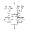
- the full bridge circuit 132 [1] includes output transistors M1 [1] and M2 [1] configured as P-channel MOSFETs, and output transistors M3 [1] and M4 [1] configured as N-channel MOSFETs. ] And.
- the full bridge circuit 132 [2] includes output transistors M1 [2] and M2 [2] configured as P-channel MOSFETs, and output transistors M3 [2] and M4 [2] configured as N-channel MOSFETs. ] And.
- a parasitic diode in the forward direction from the drain to the source is added to the P-channel MOSFET, and a parasitic diode in the forward direction from the source to the drain is added to the N-channel MOSFET. In FIG. 1, the illustration of each parasitic diode is omitted.
- the sources of the output transistors M1 [i] and M2 [i] are commonly connected to the power supply terminal VCS [i], and are connected to the sources of the output transistors M1 [i] and M2 [i]. Power supply voltage VCS is added.
- the drains of the output transistors M1 [i] and M3 [i] are commonly connected to the output terminals A OUT [i]
- the drains of the output transistors M2 [i] and M4 [i] are connected to each other. Is commonly connected to the output terminal B OUT [i]
- the sources of the output transistors M3 [i] and M4 [i] are commonly connected to the resistance connection terminal RNF [i].
- the full bridge circuit 132 [i] is configured by using the P channel type MOSFET and the N channel type MOSFET is given, but all the output transistors constituting the full bridge circuit 132 [i] are N. It may be a channel type MOSFET. At this time, necessary circuit changes are carried out. Further, the full bridge circuit 132 [i] may be configured by using a bipolar transistor instead of the MOSFET.
- the target of the value of the output current I OUT [i] is referred to as the target current value.
- the target current value for the output current I OUT [1] is represented by the symbol “I TG [1]”
- the target current value for the output current I OUT [2] is represented by the symbol “I TG [2]”.
- the magnitude (absolute value) of the target current value I TG [i] corresponds to the target of the magnitude of the output current I OUT [i] (hereinafter referred to as the target magnitude), and is determined by the reference voltage V REF [i].
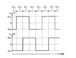
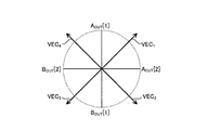
- each state can be realized in the order of states ST 4 , ST 3 , ST 2 , and ST 1 , in which case the rotor 210 moves in the second rotation direction opposite to the first rotation direction.
- the electric angle is rotated in steps of 90 °, and at this time, the mechanical angle of the rotor 210 is rotated stepwise in the second rotation direction by an angle corresponding to the amount of change in the electric angle.
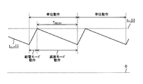
- the motor driver 100 keeps the value of the output current I OUT [i] in the vicinity of the target current value I TG [i] by PWM constant current control.
- PWM is an abbreviation for "pulse width modulation”.
- the terminal to which the power supply voltage VCS is applied is grounded via the output transistor M1 [i], the motor coil L [i], the output transistor M4 [i], and the resistor R [i].
- a positive output current I OUT [i] flows toward it, and the magnitude of the output current I OUT [i] increases with the passage of time.
- the operation realized by putting the output stage circuit 130 [i] into the power supply state corresponds to the power supply mode operation.
- the output stage circuit 130 [i] is set to the fast attenuation state, which is a kind of attenuation state.
- the fact that the output stage circuit 130 [i] is in the fast attenuation state means that the full bridge circuit 132 [i] is in the fast attenuation state.
- a polygonal line 623 with an arrow indicated by a broken line represents the flow of the output current I OUT [i] in the fast attenuation state.
- the output transistors M3 [i] are turned on and the output transistors M1 [i], M2 [i] and M4 [i] are turned off.
- a positive output current I OUT [i] flows toward the terminal to which the power supply voltage VCS is applied, and the magnitude of the output current I OUT [i] decreases with the passage of time.
- the operation realized by putting the output stage circuit 130 [i] into the fast attenuation state is a kind of attenuation mode operation.
- the external force detection unit 160 By providing the external force detection unit 160, it is possible to recognize the rotation of the rotor 210 due to an external force not intended on the system side in the motor driver 100 and the motor drive system SYS, and it is possible to take necessary measures. It becomes. For example, it is possible to issue a warning to the user or perform a predetermined error process when an external force is applied to the paper feed unit as described above. This leads to the stability of the device incorporating the motor drive system SYS.
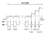
- the external force detection unit 160 receives a signal indicating the detection result of the output current I OUT [1] in order to detect the current slope SLP.
- the signal indicating the detection result of the output current I OUT [1] may be the detection voltage V RNF [1] obtained by using the resistor R [1], or the resistor. It may be a signal obtained by using a current sensor other than R [1].
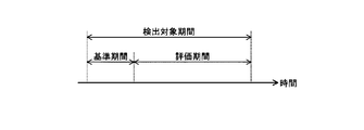
- the detection target period includes the first period and the second period after the first period, and the external force detecting unit detects 1 in the first period.
- the presence or absence of the external force applied during the second period is detected based on the comparison between the reference inclination and the inclination during the second period (11th). Configuration) may be used.
- the external force detection unit transmits a predetermined detection signal to the external device of the driver device when the application of the external force is detected. (14th configuration) may be used.
- a plurality of coils are provided in the stepping motor as the coils, and in the driver device, a plurality of channel circuits are assigned to the plurality of coils, and the output is output for each of the channel circuits.
- a stage circuit and the control circuit may be provided, and the rotor may rotate by controlling the output current in each channel circuit (16th configuration).
Landscapes
- Engineering & Computer Science (AREA)
- Power Engineering (AREA)
- Control Of Stepping Motors (AREA)
- Control Of Linear Motors (AREA)
Priority Applications (3)
| Application Number | Priority Date | Filing Date | Title |
|---|---|---|---|
| JP2022510030A JP7549000B2 (ja) | 2020-03-27 | 2021-03-18 | ドライバ装置 |
| CN202180024415.0A CN115336164A (zh) | 2020-03-27 | 2021-03-18 | 驱动器装置 |
| US17/913,371 US12132434B2 (en) | 2020-03-27 | 2021-03-18 | Driver device |
Applications Claiming Priority (2)
| Application Number | Priority Date | Filing Date | Title |
|---|---|---|---|
| JP2020058197 | 2020-03-27 | ||
| JP2020-058197 | 2020-03-27 |
Publications (1)
| Publication Number | Publication Date |
|---|---|
| WO2021193335A1 true WO2021193335A1 (ja) | 2021-09-30 |
Family
ID=77891715
Family Applications (1)
| Application Number | Title | Priority Date | Filing Date |
|---|---|---|---|
| PCT/JP2021/011016 Ceased WO2021193335A1 (ja) | 2020-03-27 | 2021-03-18 | ドライバ装置 |
Country Status (4)
| Country | Link |
|---|---|
| US (1) | US12132434B2 (https=) |
| JP (1) | JP7549000B2 (https=) |
| CN (1) | CN115336164A (https=) |
| WO (1) | WO2021193335A1 (https=) |
Families Citing this family (1)
| Publication number | Priority date | Publication date | Assignee | Title |
|---|---|---|---|---|
| CN117834583B (zh) * | 2023-12-08 | 2024-08-30 | 南京智数科技有限公司 | 一种公辅车间的继电保护管理系统及方法 |
Citations (6)
| Publication number | Priority date | Publication date | Assignee | Title |
|---|---|---|---|---|
| JPS6046798A (ja) * | 1983-08-23 | 1985-03-13 | Hitachi Ltd | ステツプモ−タ脱調検出装置 |
| JPH10285995A (ja) * | 1997-04-11 | 1998-10-23 | Sharp Corp | ステップモータ制御装置 |
| JPH11262295A (ja) * | 1998-03-12 | 1999-09-24 | Kojima Press Co Ltd | ステッピングモータの回転制御方法及び装置並びにそれを用いた車両用空気吹出口装置における風向部材の回動制御方法 |
| JP2008022639A (ja) * | 2006-07-13 | 2008-01-31 | Seiko Epson Corp | 電動モータ |
| JP2011117974A (ja) * | 2011-02-25 | 2011-06-16 | Citizen Holdings Co Ltd | アナログ電子時計 |
| JP2016208727A (ja) * | 2015-04-24 | 2016-12-08 | ローム株式会社 | モータ駆動装置及びモータ駆動装置の駆動方法 |
Family Cites Families (6)
| Publication number | Priority date | Publication date | Assignee | Title |
|---|---|---|---|---|
| JP4298141B2 (ja) | 2000-06-30 | 2009-07-15 | キヤノン株式会社 | 画像形成装置 |
| WO2008007544A2 (en) * | 2006-07-10 | 2008-01-17 | Seiko Epson Corporation | Electric motor, method for correcting sensor output for the same, and control circuit |
| US7630620B2 (en) * | 2007-07-24 | 2009-12-08 | Honeywell International Inc. | Apparatus and method for measuring an acceleration to determine a camera dome's required motor holding current |
| JP2009213344A (ja) * | 2008-02-04 | 2009-09-17 | Rohm Co Ltd | モータドライバ回路 |
| WO2012102232A1 (ja) * | 2011-01-25 | 2012-08-02 | ローム株式会社 | ステッピングモータの駆動回路、その集積回路およびそれを備える電子機器、ならびに、ステッピングモータの駆動回路の制御方法 |
| US9735773B2 (en) * | 2014-04-29 | 2017-08-15 | Allegro Microsystems, Llc | Systems and methods for sensing current through a low-side field effect transistor |
-
2021
- 2021-03-18 JP JP2022510030A patent/JP7549000B2/ja active Active
- 2021-03-18 WO PCT/JP2021/011016 patent/WO2021193335A1/ja not_active Ceased
- 2021-03-18 CN CN202180024415.0A patent/CN115336164A/zh active Pending
- 2021-03-18 US US17/913,371 patent/US12132434B2/en active Active
Patent Citations (6)
| Publication number | Priority date | Publication date | Assignee | Title |
|---|---|---|---|---|
| JPS6046798A (ja) * | 1983-08-23 | 1985-03-13 | Hitachi Ltd | ステツプモ−タ脱調検出装置 |
| JPH10285995A (ja) * | 1997-04-11 | 1998-10-23 | Sharp Corp | ステップモータ制御装置 |
| JPH11262295A (ja) * | 1998-03-12 | 1999-09-24 | Kojima Press Co Ltd | ステッピングモータの回転制御方法及び装置並びにそれを用いた車両用空気吹出口装置における風向部材の回動制御方法 |
| JP2008022639A (ja) * | 2006-07-13 | 2008-01-31 | Seiko Epson Corp | 電動モータ |
| JP2011117974A (ja) * | 2011-02-25 | 2011-06-16 | Citizen Holdings Co Ltd | アナログ電子時計 |
| JP2016208727A (ja) * | 2015-04-24 | 2016-12-08 | ローム株式会社 | モータ駆動装置及びモータ駆動装置の駆動方法 |
Also Published As
| Publication number | Publication date |
|---|---|
| CN115336164A (zh) | 2022-11-11 |
| US20230129142A1 (en) | 2023-04-27 |
| JPWO2021193335A1 (https=) | 2021-09-30 |
| US12132434B2 (en) | 2024-10-29 |
| JP7549000B2 (ja) | 2024-09-10 |
Similar Documents
| Publication | Publication Date | Title |
|---|---|---|
| TWI629867B (zh) | 流經低側場效電晶體之電流的感測系統及方法 | |
| US8659259B2 (en) | Stepping motor driving apparatus | |
| US9780706B2 (en) | Motor control current zero crossing detector | |
| CN111034016B (zh) | 用于步进马达的谐振阻尼的方法和电路组件 | |
| US8159176B2 (en) | Motor driving device | |
| US10084402B2 (en) | Microstepper motor control circuit PWM output coupled to H-bridge gates | |
| US11088641B2 (en) | Motor driving device having lock protection mode | |
| US6778417B2 (en) | Electric-power supplying devices switching between a synchronous rectification and a diode rectification by gradually altering a switching pulse | |
| US10944341B2 (en) | Energy recovery from a spindle motor using a sequence of a braking phase, an active step-up phase and an active braking phase in response to external power supply failure | |
| US8692491B2 (en) | Brushless motor driver and brushless motor system | |
| WO2021193364A1 (ja) | ステッピングモータ用のドライバ装置 | |
| US9178451B2 (en) | Controller for brushless DC motor with flexible startup and method therefor | |
| WO2021193335A1 (ja) | ドライバ装置 | |
| US8963467B2 (en) | Motor driving device and method of controlling the same | |
| US7211973B1 (en) | System and process for utilizing back electromotive force in disk drives | |
| US8829837B2 (en) | Driving apparatus for an electromagnetic load and related method | |
| KR20060115913A (ko) | 모터 드라이브 회로의 파워 트랜지스터 보호 회로, 모터드라이브 회로 및 반도체 장치 | |
| US11012013B2 (en) | Control device of motor, control system, and control method | |
| US12587115B2 (en) | Driving circuit for motor systems and control method thereof | |
| JP2002354893A (ja) | ステップモータの回転制御装置 | |
| JP4481752B2 (ja) | モータ制御装置 | |
| US20230179129A1 (en) | Motor driving device, motor system and electrical device | |
| US20260066819A1 (en) | Differential h-bridge driver | |
| JP2023046828A (ja) | モータ駆動装置、モータシステム、及び電気機器 | |
| JPH1189288A (ja) | ステッピングモータ駆動装置 |
Legal Events
| Date | Code | Title | Description |
|---|---|---|---|
| 121 | Ep: the epo has been informed by wipo that ep was designated in this application |
Ref document number: 21777169 Country of ref document: EP Kind code of ref document: A1 |
|
| ENP | Entry into the national phase |
Ref document number: 2022510030 Country of ref document: JP Kind code of ref document: A |
|
| NENP | Non-entry into the national phase |
Ref country code: DE |
|
| 122 | Ep: pct application non-entry in european phase |
Ref document number: 21777169 Country of ref document: EP Kind code of ref document: A1 |