WO2021187457A1 - 平面フィルタ - Google Patents
平面フィルタ Download PDFInfo
- Publication number
- WO2021187457A1 WO2021187457A1 PCT/JP2021/010521 JP2021010521W WO2021187457A1 WO 2021187457 A1 WO2021187457 A1 WO 2021187457A1 JP 2021010521 W JP2021010521 W JP 2021010521W WO 2021187457 A1 WO2021187457 A1 WO 2021187457A1
- Authority
- WO
- WIPO (PCT)
- Prior art keywords
- line
- width
- input
- region
- dielectric substrate
- Prior art date
- Legal status (The legal status is an assumption and is not a legal conclusion. Google has not performed a legal analysis and makes no representation as to the accuracy of the status listed.)
- Ceased
Links
Images


Classifications
-
- H—ELECTRICITY
- H01—ELECTRIC ELEMENTS
- H01P—WAVEGUIDES; RESONATORS, LINES, OR OTHER DEVICES OF THE WAVEGUIDE TYPE
- H01P1/00—Auxiliary devices
- H01P1/20—Frequency-selective devices, e.g. filters
- H01P1/201—Filters for transverse electromagnetic waves
- H01P1/203—Strip line filters
- H01P1/20327—Electromagnetic interstage coupling
- H01P1/20354—Non-comb or non-interdigital filters
- H01P1/20372—Hairpin resonators
-
- H—ELECTRICITY
- H01—ELECTRIC ELEMENTS
- H01P—WAVEGUIDES; RESONATORS, LINES, OR OTHER DEVICES OF THE WAVEGUIDE TYPE
- H01P1/00—Auxiliary devices
- H01P1/20—Frequency-selective devices, e.g. filters
- H01P1/201—Filters for transverse electromagnetic waves
- H01P1/203—Strip line filters
-
- H—ELECTRICITY
- H01—ELECTRIC ELEMENTS
- H01P—WAVEGUIDES; RESONATORS, LINES, OR OTHER DEVICES OF THE WAVEGUIDE TYPE
- H01P7/00—Resonators of the waveguide type
- H01P7/08—Strip line resonators
Definitions
- the embodiment relates to a planar filter.
- the planar filter provided on the dielectric substrate is used in a high frequency band of several GHz or more, and is configured by combining, for example, distributed constant lines. Therefore, there is a limit to the miniaturization of the planar filter.
- the embodiment provides a miniaturized planar filter.
- the planar filter according to the embodiment includes a dielectric substrate, a filter unit provided on the dielectric substrate, and an input / output line connected to the filter unit on the dielectric substrate.
- the dielectric substrate has a first region having a first thickness in a first direction from the back surface opposite to the front surface on which the filter portion and the input / output line are provided toward the front surface, and is thinner than the first thickness. It includes a second region having a second thickness in the first direction, and has a step corresponding to the difference between the first thickness and the second thickness on the back surface side.
- the filter unit is provided in the first region, and the input / output line is provided in the second region.
- each part will be described using the X-axis, Y-axis and Z-axis shown in each figure.
- the X-axis, Y-axis, and Z-axis are orthogonal to each other and represent the X-direction, the Y-direction, and the Z-direction, respectively. Further, the Z direction may be described as upward, and the opposite direction may be described as downward.
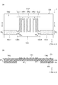
- FIG. 1A and 1B are schematic views showing a planar filter 1 according to an embodiment.
- FIG. 1A is a plan view showing the surface of the dielectric substrate DS.
- FIG. 1B is a cross-sectional view taken along the line AA shown in FIG. 1A.
- the planar filter 1 includes a dielectric substrate DS, a filter unit FLP, an input / output line IOL1, and an input / output line IOL2.
- the planar filter 1 is composed of a plurality of distributed constant lines provided on the surface of the dielectric substrate DS.
- the dielectric substrate DS includes a first region TR1 and a second region TR2.
- the filter unit FLP is provided on the first region TR1.
- the input / output lines IOL1 and IOL2 are provided on the second region TR2.
- the dielectric substrate DS is, for example, a PPE resin substrate.
- the filter unit FLP is provided between the input / output line IOL1 and the input / output line IOL2.
- the input / output line IOL1, the filter unit FLP, and the input / output line IOL2 are arranged side by side in a direction (for example, the X direction) along the surface of the dielectric substrate DS.
- the input / output line IOL1 and the input / output line IOL2 each extend in the X direction and are connected to the filter unit FLP.
- the input / output line IOL1 and the input / output line IOL2 each have a line width W 0 in a direction (for example, the Y direction) along the surface of the dielectric substrate DS.
- the microwave signal is input to the input / output line IOL1 and output from the input / output line IOL2 via the filter unit FLP. Further, the microwave signal may be input to the input / output line IOL2 and output from the input / output line IOL1 via the filter unit FLP.
- the filter unit FLP includes, for example, a resonator HR1, a resonator HR2, a resonator HR3, a first coupling line CL1, a second coupling line CL2, a connecting line IOLA, and a connecting line IOLB.
- the resonators HR1 to HR3 are separated from each other and are arranged side by side in the X direction, for example.
- the resonator HR2 is provided between the resonator HR1 and the resonator HR3.
- the first coupling line CL1 is provided between the connecting line IOLA and the resonator HR1.
- the first coupling line CL1 is connected to the connecting line IOLA. Further, the first coupling line CL1 is arranged apart from the resonator HR1.
- the second coupling line CL2 is provided between the connecting line IOLB and the resonator HR3.
- the second coupling line CL2 is connected to the connecting line IOLB. Further, the second coupling line CL2 is arranged apart from the resonator HR3.
- the input / output line IOLA is provided between the first coupling line CL1 and the input / output line IOL1.
- the input / output line IOLA is connected to the input / output line IOL1 at the boundary between the first region TR1 and the second region TR2. Further, the input / output line IOLA is connected to the first coupling line CL1 on the first region TR1.
- the input / output line IOLA has, for example, a width W 0A in the Y direction. Width W 0A is smaller than the width W 0 of the Y direction of the input and output lines IOL1.
- the impedance discontinuity of the line can be reduced, and the reflection of microwaves between the input / output line IOL1 and the first coupling line CL1 can be reduced.
- the input / output line IOLB is provided between the second coupling line CL2 and the input / output line IOL2.
- the input / output line IOLB is connected to the input / output line IOL2 at the boundary between the first region TR1 and the second region TR2. Further, the input / output line IOLB is connected to the second coupling line CL2 on the first region TR1.
- the input / output line IOLB has, for example, a width W 0B in the Y direction. Width W 0B is narrower than the width W 0 of the Y direction of the input and output lines IOL2.
- the impedance discontinuity of the line can be reduced, and the reflection of microwaves between the input / output line IOL2 and the second coupling line CL2 can be reduced.
- the input / output line IOL1, the input / output line IOL2, the resonators HR1 to HR3, the first coupling line CL1 and the second coupling line LI2 are metal layers provided on the dielectric substrate DS, for example, copper (Cu). )including.
- the dielectric substrate DS has a first thickness ST 1 and a second thickness ST 2 in a direction (for example, the Z direction) from the back surface BS to the front surface FS.
- the first thickness ST 1 is thinner than the second thickness ST 2.
- the dielectric substrate DS has a first thickness ST 1 in the first region TR1 and a second thickness ST 2 in the second region TR2. Further, the dielectric substrate DS has, for example, a step corresponding to the difference ⁇ T between the first thickness ST 1 and the second thickness ST 2 at the boundary between the first region TR1 and the second region TR2 on the back surface BS side. ..
- the dielectric substrate DS includes a metal layer 10 that covers the back surface BS.
- the metal layer 10 contains, for example, copper (Cu).
- the metal layer 10 is provided so as to cover a step on the back surface BS side of the dielectric substrate DS.
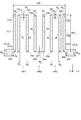
- FIG. 2 is a partial plan view schematically showing the plane filter 1 according to the embodiment.
- FIG. 2 is a schematic view showing the filter unit FLP.
- the first resonator HR1 includes a first line 13, a second line 15, and a third line 17.
- the first line 13 and the second line 15 extend in a direction (for example, the Y direction) along the surface FS of the dielectric substrate DS, respectively.
- the first line 13 and the second line 15 are arranged so as to face each other and to be separated from each other.
- the first line 13 includes a first end 13a and a second end 13b arranged in order in the Y direction.
- the second line 15 includes a first end 15a and a second end 15b arranged in order in the Y direction.
- the third line 17 extends in the X direction, for example, and is connected to the second end 13b of the first line 13 and the second end 15b of the second line 15.
- the second resonator HR2 includes a fourth line 23, a fifth line 25, and a sixth line 27.
- the fourth line 23 and the fifth line 25 extend in the Y direction, respectively.
- the fourth line 23 and the fifth line 25 are arranged so as to face each other and to be separated from each other.
- the fourth line 23 includes a first end 23a and a second end 23b arranged in order in the Y direction.
- the fifth line 25 includes a first end 25a and a second end 25b arranged in order in the Y direction.
- the sixth line 27 extends in the X direction, for example, and is connected to the first end 23a of the fourth line 23 and the first end 25a of the fifth line 25.
- the third resonator HR3 includes a seventh line 33, an eighth line 35, and a ninth line 37.
- the seventh line 33 and the eighth line 35 extend in the Y direction, respectively.
- the seventh line 33 and the eighth line 35 are arranged so as to face each other and to be separated from each other.
- the seventh line 33 includes a first end 33a and a second end 33b arranged in order in the Y direction.
- the eighth line 35 includes a first end 35a and a second end 35b arranged in order in the Y direction.
- the ninth line 27 extends in the X direction, for example, and is connected to the second end 33b of the seventh line 33 and the second end 25b of the eighth line 35.
- the first resonator HR1 and the second resonator HR2 are separated from each other and are arranged in the X direction, and the second line 15 of the first resonator HR1 faces the fourth line 23 of the second resonator HR2. Further, the first end 15a of the second line 15 faces the first end 23a of the fourth line 23, and the second end 35b of the second line 15 faces the second end 23b of the fourth line 23.
- the second resonator HR2 and the third resonator HR3 are separated from each other and lined up in the X direction, and the fifth line 25 of the second resonator HR2 faces the seventh line 33 of the third resonator HR3. Further, the first end 25a of the fifth line 25 faces the first end 33a of the seventh line 33, and the second end 25b of the fifth line 25 faces the second end 33b of the seventh line 33.
- the first coupling line CL1 extends in the Y direction and faces the first line 13 of the first resonator HR1 in the X direction.
- the first coupling line CL1 has a first end CLa and a second end CLb arranged in order in the Y direction, and is connected to the connection line IOLA at the first end CLa. Further, the first end CLa of the first coupling line CL1 faces the first end 13a of the first line 13, and the second end CLb of the first coupling line CL1 faces the second end 13b of the first line 13. do.
- the second coupling line CL2 extends in the Y direction and faces the eighth line 35 of the third resonator HR3 in the X direction.
- the second coupling line CL2 has a first end CLa and a second end CLb arranged in order in the Y direction, and is connected to the connection line IOLB at the first end CLa. Further, the first end CLa of the second coupling line CL2 faces the first end 35a of the eighth line 35, and the second end CLb of the second coupling line CL2 faces the second end 35b of the eighth line 35. do.
- the first coupling line CL1 is connected to the end of the connecting line IOLA in the X direction.
- the first coupling line CL1 is connected at a position where the first end CLa is shifted in the Y direction by ⁇ W from one of the two corners of the end of the connecting line IOLA. For example, when the width of the connection line IOLA in the Y direction is W 0A , the first coupling line CL1 is connected to the connection line IOLA with a connection width of W 0A ⁇ ⁇ W.
- the second coupling line CL2 is similarly connected to the end of the connecting line IOLB in the X direction. That is, the second coupling line CL2 is connected at a position where the first end CLa is shifted in the Y direction by ⁇ W from one of the two corners of the end of the connecting line IOLB. For example, when the width of the connection line IOLB in the Y direction is W 0B , the second coupling line CL2 is connected to the connection line IOLB with a connection width of W 0B ⁇ W.
- the widths W 1 , W 2 , W 4 , W 5 , W 7 and W 8 are substantially the same.
- the width W 3 in the Y direction of the third line 17, the width W 6 in the Y direction of the sixth line 27, and the width W 9 in the Y direction of the ninth line 37 are narrower than, for example, the width W 0.
- the widths W 3 , W 6 and W 9 are substantially the same.
- the first line 13 to the ninth line 37, the first coupling line CL1 and the second coupling line CL2 each have a characteristic impedance of 85 ⁇ , for example.
- the first connection line IOLA, the second connection line IOLB, the input / output line IOL1 and the input / output line IOL2 each have a characteristic impedance of 50 ⁇ , for example.
- the filter unit FLP is provided on the first region TR1, the width W 1 ⁇ W 9 of the first line 13 to the ninth line 37, the width W C1 of the X direction of the first coupled line CL1 and the second coupling line
- the width W C2 of CL2 in the X direction is narrower than, for example, when the filter portion FLP is provided on the dielectric substrate which does not have the first region TR1. Further, the distance between adjacent lines in the X direction can be reduced. As a result, the width WF 1 of the filter unit FLP in the X direction becomes narrower than, for example, when it is provided on a dielectric substrate that does not have the first region TR1.
- the planar filter 1 is downsized as compared with the case where it is provided on a dielectric substrate that does not have the first region TR1.
- the width WF 2 of the filter unit FLP in the Y direction is substantially the same as, for example, ⁇ / 4 ( ⁇ : wavelength of microwave).
- the planar filter 1 can be miniaturized while maintaining the mechanical strength of the dielectric substrate DS.
- FIG. 3 is a graph showing the characteristics of the planar filter 1 according to the embodiment.
- the horizontal axis is the frequency of the microwave (GHz), and the vertical axis is the transmission coefficient (dB) and the reflection coefficient (dB) of the microwave.
- the planar filter 1 is a bandpass filter having a center frequency of 20 GHz.
- the pass characteristic is about minus 2.8 dB, and the pass bandwidth is about 1.5 GHz.
- the dielectric substrate DS is a PPE resin substrate.
- the first thickness ST 1 of the first region TR1 is 0.2 mm
- the second thickness ST 2 of the second region TR2 is 0.4 mm.
- the width WF 1 in the X direction of the filter unit FLP is 2.95 mm
- the width WF 2 in the Y direction is 2.25 mm.
- the planar filter 4 shown in FIG. 6 is provided on a dielectric substrate having a thickness of 0.4 mm in the Z direction.
- the planar filter 4 is provided on a dielectric substrate having a uniform thickness and does not have the first region TR1.
- the planar filter 4 has the same passing characteristics as the planar filter 1, and the width of the filter portion FLP in the planar filter 4 in the X direction is 4.3 mm. That is, in the planar filter 1 according to the embodiment, it is possible to reduce the surface area of the dielectric substrate by about 35% without changing the passing characteristics.
- FIG. 4 is a schematic view showing a plane filter 2 according to the first modification of the embodiment.
- the flat filter 2 has a filter unit FLP provided on the surface of the dielectric substrate DS, an input / output line IOL1 and an input / output line IOL2.
- the filter unit FLP is provided on the first region TR1.
- the input / output lines IOL1 and IOL2 are provided on the second region TR2.
- the filter unit FLP includes a resonator HR1, a resonator HR2, a first coupling line CL1, a second coupling line CL2, a connecting line IOLA, and a connecting line IOLB.
- the arrangement of the input / output line IOL1, the connection line IOLA, the first coupling line CL1 and the resonator HR1 is the same as that of the planar filter 1.
- the second coupling line CL2 is provided between the resonator HR2 and the connecting line IOLB, and is arranged so as to face the fifth line 25 of the resonator HR2.
- the first end 25a of the fifth line 25 faces the first end CLa of the second coupling line CL2.
- the second end 25b of the fifth line 25 faces the second end CLb of the second coupling line CL2.
- the connection line IOLB is connected to the second end CLb of the second coupling line CL2.
- connection line IOLB is connected to the input / output line IOL2 at the boundary between the first region TR1 and the second region TR2.
- the input / output line IOL2 extends in the X direction along the surface of the dielectric substrate DS.
- the resonators HR1 to HR2 are appropriately arranged between the first coupling line CL1 and the second coupling line CL2 in order to obtain desired filter characteristics.
- the number of resonators is not limited to these examples, and for example, three or more resonators may be arranged between the first coupling line CL1 and the second coupling line CL2.
- FIG. 5 (a) and 5 (b) are schematic views showing a plane filter 3 according to a third modification of the embodiment.
- FIG. 5A is a plan view showing the surface of the dielectric substrate DS.
- FIG. 5B is a cross-sectional view taken along the line BB shown in FIG. 5A.
- the flat filter 3 has a filter unit FLP provided on the surface of the dielectric substrate DS, an input / output line IOL1 and an input / output line IOL2.
- the filter unit FLP is provided on the first region TR1.
- the input / output lines IOL1 and IOL2 are provided on the second region TR2.
- the dielectric substrate DS further includes the third region TR3.
- the third region TR3 is provided between the first region TR1 and the second region TR2.
- the planar filter 3 further includes a connection line IOLA and a connection line IOLB provided over the first region TR1 and the third region TR3.
- connection line IOLA is provided between the first coupling line CL1 and the input / output line IOL1.
- the connection line IOLA is connected to the input / output line IOL1 at the boundary between the second region TR2 and the third region TR3. Further, the connection line IOLA is connected to the first coupling line CL1 in the first region TR1.
- connection line IOLA has, for example, a width W 0 in the Y direction at the boundary between the second region TR2 and the third region TR3. Further, the connection line IOLA has a width W 0A in the Y direction on the first region TR. Further, it has a width W 0A in the Y direction at the boundary between the first region TR1 and the third region TR3. The width W 0A is narrower than the width W 0. The width of the connection line IOLA in the Y direction narrows as it approaches the boundary between the first region TR1 and the third region TR3 from the boundary between the second region TR2 and the third region TR3.
- connection line IOLB is provided between the second coupling line CL2 and the input / output line IOL2.
- the connection line IOLB is connected to the input / output line IOL2 at the boundary between the second region TR2 and the third region TR3.
- connection line IOLA is connected to the second coupling line CL1 in the first region TR1.
- connection line IOLB has a width W 0 in the Y direction at the boundary between the second region TR2 and the third region TR3, for example. Further, the connection line IOLB has a width W 0B in the Y direction on the first region TR1. Further, it has a width W 0B in the Y direction at the boundary between the first region TR1 and the third region TR3. The width W 0B is narrower than the width W 0. The width of the connection line IOLB in the Y direction narrows as it approaches the boundary between the first region TR1 and the third region TR3 from the boundary between the second region TR2 and the third region TR3.
- the dielectric substrate DS has, for example, a second thickness ST 2 at the boundary between the second region TR2 and the third region TR3. Further, the dielectric substrate DS has a first thickness ST 1 at the boundary between the first region TR1 and the third region TR3. That is, the third thickness ST 3 of the third region TR3 becomes thinner as it approaches the first region TR1.
- the dielectric substrate DS has the first position P 1 in the third region TR3, a third thickness ST 3A, the third thickness ST 3B in the second position P 2.
- the first position P 1 is located between the first region TR 1 and the second position P 2, and the third thickness ST 3A is thinner than the third thickness ST 3B.
- connection line IOLA and the connection line IOLB are provided so as to have a characteristic impedance of 50 ⁇ , for example.
- the reflection of microwaves between the input / output line IOL1 and the first coupling line CL1 and between the input / output line IOL2 and the second coupling line CL2 can be further reduced.
Landscapes
- Physics & Mathematics (AREA)
- Electromagnetism (AREA)
- Control Of Motors That Do Not Use Commutators (AREA)
Priority Applications (3)
| Application Number | Priority Date | Filing Date | Title |
|---|---|---|---|
| EP21772612.4A EP4123822A4 (en) | 2020-03-17 | 2021-03-16 | Planar filter |
| US17/906,589 US12244046B2 (en) | 2020-03-17 | 2021-03-16 | Plane filter |
| JP2022508365A JP7414959B2 (ja) | 2020-03-17 | 2021-03-16 | 平面フィルタ |
Applications Claiming Priority (2)
| Application Number | Priority Date | Filing Date | Title |
|---|---|---|---|
| JP2020-046515 | 2020-03-17 | ||
| JP2020046515 | 2020-03-17 |
Publications (1)
| Publication Number | Publication Date |
|---|---|
| WO2021187457A1 true WO2021187457A1 (ja) | 2021-09-23 |
Family
ID=77770930
Family Applications (1)
| Application Number | Title | Priority Date | Filing Date |
|---|---|---|---|
| PCT/JP2021/010521 Ceased WO2021187457A1 (ja) | 2020-03-17 | 2021-03-16 | 平面フィルタ |
Country Status (4)
| Country | Link |
|---|---|
| US (1) | US12244046B2 (https=) |
| EP (1) | EP4123822A4 (https=) |
| JP (1) | JP7414959B2 (https=) |
| WO (1) | WO2021187457A1 (https=) |
Families Citing this family (2)
| Publication number | Priority date | Publication date | Assignee | Title |
|---|---|---|---|---|
| US12394875B2 (en) | 2020-08-25 | 2025-08-19 | Fujikura Ltd. | Filter device comprising a substrate having strip-shaped conductors and ground recesses of lengths longer than the strip-shaped conductors |
| CN115428255B (zh) * | 2020-08-25 | 2025-07-11 | 株式会社藤仓 | 滤波器装置 |
Citations (3)
| Publication number | Priority date | Publication date | Assignee | Title |
|---|---|---|---|---|
| JPH07212111A (ja) * | 1994-01-20 | 1995-08-11 | Fujitsu General Ltd | マイクロストリップ回路 |
| JPH09232807A (ja) | 1996-02-28 | 1997-09-05 | Ngk Spark Plug Co Ltd | 二帯域フィルタ |
| JP2011061296A (ja) * | 2009-09-07 | 2011-03-24 | Sharp Corp | 高周波回路および受信装置 |
Family Cites Families (3)
| Publication number | Priority date | Publication date | Assignee | Title |
|---|---|---|---|---|
| US6483404B1 (en) * | 2001-08-20 | 2002-11-19 | Xytrans, Inc. | Millimeter wave filter for surface mount applications |
| US6667549B2 (en) * | 2002-05-01 | 2003-12-23 | Bridgewave Communications, Inc. | Micro circuits with a sculpted ground plane |
| TWI462385B (zh) | 2009-05-26 | 2014-11-21 | Wistron Neweb Corp | 自我匹配之帶通濾波器及其相關降頻器 |
-
2021
- 2021-03-16 WO PCT/JP2021/010521 patent/WO2021187457A1/ja not_active Ceased
- 2021-03-16 US US17/906,589 patent/US12244046B2/en active Active
- 2021-03-16 JP JP2022508365A patent/JP7414959B2/ja active Active
- 2021-03-16 EP EP21772612.4A patent/EP4123822A4/en active Pending
Patent Citations (3)
| Publication number | Priority date | Publication date | Assignee | Title |
|---|---|---|---|---|
| JPH07212111A (ja) * | 1994-01-20 | 1995-08-11 | Fujitsu General Ltd | マイクロストリップ回路 |
| JPH09232807A (ja) | 1996-02-28 | 1997-09-05 | Ngk Spark Plug Co Ltd | 二帯域フィルタ |
| JP2011061296A (ja) * | 2009-09-07 | 2011-03-24 | Sharp Corp | 高周波回路および受信装置 |
Non-Patent Citations (1)
| Title |
|---|
| See also references of EP4123822A4 |
Also Published As
| Publication number | Publication date |
|---|---|
| US20230049841A1 (en) | 2023-02-16 |
| JPWO2021187457A1 (https=) | 2021-09-23 |
| EP4123822A1 (en) | 2023-01-25 |
| EP4123822A4 (en) | 2024-04-17 |
| JP7414959B2 (ja) | 2024-01-16 |
| US12244046B2 (en) | 2025-03-04 |
Similar Documents
| Publication | Publication Date | Title |
|---|---|---|
| US8314667B2 (en) | Coupled line filter and arraying method thereof | |
| US7429902B2 (en) | Differential transmission line having a curved region with selected radius of curvature | |
| US5977847A (en) | Microstrip band elimination filter | |
| JP7414959B2 (ja) | 平面フィルタ | |
| US20210151850A1 (en) | Power divider/combiner | |
| US20220285808A1 (en) | Distributed constant filter, distributed constant line resonator, and multiplexer | |
| US10418680B1 (en) | Multilayer coupler having mode-compensating bend | |
| CN107946710A (zh) | 基于rqmsiw的超紧凑双频段带通滤波器 | |
| CN219553853U (zh) | 印刷膜射频微带带通滤波器 | |
| CN115149231B (zh) | 基于基片集成悬状线的小型化双模带阻滤波器 | |
| CN218677535U (zh) | 一种无源元件的强耦合带状线结构 | |
| CN109994806A (zh) | 具有双传输零点和宽阻带的isgw宽频带通滤波器 | |
| US11228077B2 (en) | Microstrip DC block | |
| US8358184B2 (en) | Stripline filter | |
| EP1455410B1 (en) | Bandpass filter | |
| JP4411315B2 (ja) | 帯域阻止フィルタ | |
| JP6946156B2 (ja) | トラップフィルタ | |
| JP7464547B2 (ja) | 薄膜基板回路 | |
| JPH09321505A (ja) | マイクロ波回路 | |
| KR102933610B1 (ko) | 불요파 방사를 감소시키는 패치 안테나 및 이를 포함하는 세라믹 도파관 필테나 | |
| CN119581813B (zh) | 一种基于sisl的双通带滤波器 | |
| JPH04339401A (ja) | 導波管型誘電体共振器装置 | |
| CN100334776C (zh) | 带通滤波器 | |
| CN110224208B (zh) | 可抑制共模信号的差分滤波器微带线结构 | |
| EP1408576A1 (en) | Band-pass filter |
Legal Events
| Date | Code | Title | Description |
|---|---|---|---|
| 121 | Ep: the epo has been informed by wipo that ep was designated in this application |
Ref document number: 21772612 Country of ref document: EP Kind code of ref document: A1 |
|
| ENP | Entry into the national phase |
Ref document number: 2022508365 Country of ref document: JP Kind code of ref document: A |
|
| NENP | Non-entry into the national phase |
Ref country code: DE |
|
| ENP | Entry into the national phase |
Ref document number: 2021772612 Country of ref document: EP Effective date: 20221017 |
|
| WWG | Wipo information: grant in national office |
Ref document number: 17906589 Country of ref document: US |