WO2021187053A1 - 出力帰還制御回路、スイッチング電源 - Google Patents
出力帰還制御回路、スイッチング電源 Download PDFInfo
- Publication number
- WO2021187053A1 WO2021187053A1 PCT/JP2021/007316 JP2021007316W WO2021187053A1 WO 2021187053 A1 WO2021187053 A1 WO 2021187053A1 JP 2021007316 W JP2021007316 W JP 2021007316W WO 2021187053 A1 WO2021187053 A1 WO 2021187053A1
- Authority
- WO
- WIPO (PCT)
- Prior art keywords
- output
- voltage
- amplifier
- signal
- error
- Prior art date
- Legal status (The legal status is an assumption and is not a legal conclusion. Google has not performed a legal analysis and makes no representation as to the accuracy of the status listed.)
- Ceased
Links
Images







Classifications
-
- H—ELECTRICITY
- H02—GENERATION; CONVERSION OR DISTRIBUTION OF ELECTRIC POWER
- H02M—APPARATUS FOR CONVERSION BETWEEN AC AND AC, BETWEEN AC AND DC, OR BETWEEN DC AND DC, AND FOR USE WITH MAINS OR SIMILAR POWER SUPPLY SYSTEMS; CONVERSION OF DC OR AC INPUT POWER INTO SURGE OUTPUT POWER; CONTROL OR REGULATION THEREOF
- H02M3/00—Conversion of DC power input into DC power output
- H02M3/02—Conversion of DC power input into DC power output without intermediate conversion into AC
- H02M3/04—Conversion of DC power input into DC power output without intermediate conversion into AC by static converters
- H02M3/10—Conversion of DC power input into DC power output without intermediate conversion into AC by static converters using discharge tubes with control electrode or semiconductor devices with control electrode
- H02M3/145—Conversion of DC power input into DC power output without intermediate conversion into AC by static converters using discharge tubes with control electrode or semiconductor devices with control electrode using devices of a triode or transistor type requiring continuous application of a control signal
- H02M3/155—Conversion of DC power input into DC power output without intermediate conversion into AC by static converters using discharge tubes with control electrode or semiconductor devices with control electrode using devices of a triode or transistor type requiring continuous application of a control signal using semiconductor devices only
- H02M3/156—Conversion of DC power input into DC power output without intermediate conversion into AC by static converters using discharge tubes with control electrode or semiconductor devices with control electrode using devices of a triode or transistor type requiring continuous application of a control signal using semiconductor devices only with automatic control of output voltage or current, e.g. switching regulators
- H02M3/158—Conversion of DC power input into DC power output without intermediate conversion into AC by static converters using discharge tubes with control electrode or semiconductor devices with control electrode using devices of a triode or transistor type requiring continuous application of a control signal using semiconductor devices only with automatic control of output voltage or current, e.g. switching regulators including plural semiconductor devices as final control devices for a single load
-
- H—ELECTRICITY
- H02—GENERATION; CONVERSION OR DISTRIBUTION OF ELECTRIC POWER
- H02M—APPARATUS FOR CONVERSION BETWEEN AC AND AC, BETWEEN AC AND DC, OR BETWEEN DC AND DC, AND FOR USE WITH MAINS OR SIMILAR POWER SUPPLY SYSTEMS; CONVERSION OF DC OR AC INPUT POWER INTO SURGE OUTPUT POWER; CONTROL OR REGULATION THEREOF
- H02M1/00—Details of apparatus for conversion
- H02M1/0003—Details of control, feedback or regulation circuits
-
- H—ELECTRICITY
- H02—GENERATION; CONVERSION OR DISTRIBUTION OF ELECTRIC POWER
- H02M—APPARATUS FOR CONVERSION BETWEEN AC AND AC, BETWEEN AC AND DC, OR BETWEEN DC AND DC, AND FOR USE WITH MAINS OR SIMILAR POWER SUPPLY SYSTEMS; CONVERSION OF DC OR AC INPUT POWER INTO SURGE OUTPUT POWER; CONTROL OR REGULATION THEREOF
- H02M1/00—Details of apparatus for conversion
- H02M1/0003—Details of control, feedback or regulation circuits
- H02M1/0025—Arrangements for modifying reference values, feedback values or error values in the control loop of a converter
-
- H—ELECTRICITY
- H02—GENERATION; CONVERSION OR DISTRIBUTION OF ELECTRIC POWER
- H02M—APPARATUS FOR CONVERSION BETWEEN AC AND AC, BETWEEN AC AND DC, OR BETWEEN DC AND DC, AND FOR USE WITH MAINS OR SIMILAR POWER SUPPLY SYSTEMS; CONVERSION OF DC OR AC INPUT POWER INTO SURGE OUTPUT POWER; CONTROL OR REGULATION THEREOF
- H02M3/00—Conversion of DC power input into DC power output
- H02M3/02—Conversion of DC power input into DC power output without intermediate conversion into AC
- H02M3/04—Conversion of DC power input into DC power output without intermediate conversion into AC by static converters
- H02M3/10—Conversion of DC power input into DC power output without intermediate conversion into AC by static converters using discharge tubes with control electrode or semiconductor devices with control electrode
- H02M3/145—Conversion of DC power input into DC power output without intermediate conversion into AC by static converters using discharge tubes with control electrode or semiconductor devices with control electrode using devices of a triode or transistor type requiring continuous application of a control signal
- H02M3/155—Conversion of DC power input into DC power output without intermediate conversion into AC by static converters using discharge tubes with control electrode or semiconductor devices with control electrode using devices of a triode or transistor type requiring continuous application of a control signal using semiconductor devices only
- H02M3/156—Conversion of DC power input into DC power output without intermediate conversion into AC by static converters using discharge tubes with control electrode or semiconductor devices with control electrode using devices of a triode or transistor type requiring continuous application of a control signal using semiconductor devices only with automatic control of output voltage or current, e.g. switching regulators
- H02M3/157—Conversion of DC power input into DC power output without intermediate conversion into AC by static converters using discharge tubes with control electrode or semiconductor devices with control electrode using devices of a triode or transistor type requiring continuous application of a control signal using semiconductor devices only with automatic control of output voltage or current, e.g. switching regulators with digital control
Definitions
- the invention disclosed in the present specification relates to an output feedback control circuit and a switching power supply using the same.
- a switching power supply or a servo mechanism incorporates an output feedback control circuit that controls output feedback so that the output voltage matches a predetermined reference voltage.
- Patent Document 1 can be mentioned as an example of the prior art related to the above.
- the invention disclosed in the present specification is an output feedback control circuit capable of achieving both high speed and high accuracy in view of the above-mentioned problems found by the inventors of the present application, and switching using the same.
- the purpose is to provide power.
- the output feedback control circuit disclosed in the present specification generates a first error signal according to the difference between the output voltage supplied to the load or the feedback voltage corresponding thereto and a predetermined reference voltage.
- a first amplifier a second amplifier that generates a second error signal according to the difference between the output voltage or the feedback voltage and the first error signal or the reference voltage at a speed higher than that of the first amplifier, and the load.
- the arithmetic unit that superimposes the remote sense signal drawn from the ground end on the reference voltage input to the first amplifier is connected between the application end of the first error signal and the application end of the remote sense signal. Including with a capacitor.
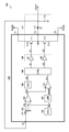
- FIG. 1 is a diagram showing a basic configuration of a switching power supply.
- FIG. 2 is a diagram showing a first embodiment of a switching power supply.
- FIG. 3 is a diagram showing a second embodiment of a switching power supply.
- FIG. 4 is a diagram showing a third embodiment of a switching power supply.
- FIG. 5 is a diagram showing a fourth embodiment of a switching power supply.
- FIG. 6 is a diagram showing a fifth embodiment of a switching power supply.
- FIG. 7 is a diagram for explaining the reason why it is difficult to achieve both high speed and high accuracy with a single amplifier.
- FIG. 8 is a diagram showing a sixth embodiment of a switching power supply.
- FIG. 9 is a diagram showing a frequency-gain characteristic in the sixth embodiment.
- FIG. 10 is a diagram showing a seventh embodiment of a switching power supply.
- FIG. 11 is a diagram showing an eighth embodiment of a switching power supply.
- FIG. 12 is a diagram showing a ninth embodiment of a switching power supply.
- FIG. 13 is a diagram showing an introduction example of the remote sense function.
- FIG. 14 is a diagram showing a tenth embodiment of a switching power supply.
- FIG. 15 is a diagram showing a frequency-gain characteristic in the tenth embodiment.
- FIG. 16 is a diagram showing an eleventh embodiment of a switching power supply.
- FIG. 17 is a diagram showing a frequency-gain characteristic in the eleventh embodiment.
- FIG. 18 is a diagram showing a twelfth embodiment of a switching power supply.
- FIG. 19 is an external view of the television.
- FIG. 20 is an external view of a personal computer.
- FIG. 21 is an external view of the smartphone.
- FIG. 1 is a diagram showing a basic configuration of a switching power supply.
- the switching power supply 100 of this configuration example is a PWM [pulse width modulation] drive type DC / DC converter that generates an output voltage VOUT from an input voltage P VDD and supplies it to a load (not shown). It has a voltage generation circuit 120, a reference voltage generation circuit 130, an error amplifier 140, a lamp signal generation circuit 150, an oscillator 160, a PWM comparator 170, a control circuit 180, and a switch drive circuit 190.
- the above components are the semiconductor integrated circuit device 200 (so-called power supply control IC) that is the main control body of the switching power supply 100, except for some components (inductor 113 and capacitor 114 in this figure) included in the switching output circuit 110. It is good to integrate in. In addition to the above, any component (various protection circuits, etc.) can be appropriately incorporated into the semiconductor integrated circuit device 200.
- the semiconductor integrated circuit device 200 has a plurality of external terminals (in this figure, a power supply terminal T1, an output terminal T2, a ground terminal T3, and a feedback terminal) as means for establishing an electrical connection with the outside of the device. (Example of four T4s) is provided.
- the switching output circuit 110 is a step-down type that drives an inductor current IL and generates an output voltage VOUT from an input voltage P VDD by turning on / off an upper switch and a lower switch connected so as to form a half bridge. It is a switching output stage and includes an output transistor 111, a synchronous rectifying transistor 112, an inductor 113, and a capacitor 114.
- the output transistor 111 is a PMOSFET [P channel type metal oxide semiconductor field effect transistor] that functions as an upper switch of the switching output stage.
- the gate of the output transistor 111 is connected to the application end of the upper gate signal G1.
- the output transistor 111 turns off when the upper gate signal G1 is at a high level and turns on when the upper gate signal G1 is at a low level.
- the inductor 113 and the capacitor 114 are discrete components externally attached to the semiconductor integrated circuit device 200, and form an LC filter that rectifies and smoothes the switch voltage SW to generate an output voltage VOUT.
- the first end of the inductor 113 is connected to the output terminal T2 of the semiconductor integrated circuit device 200.
- the second end of the inductor 113 and the first end of the capacitor 114 are connected to the application end of the output voltage VOUT and the feedback terminal T4.
- the second end of the capacitor 114 is connected to the grounded end.
- the output transistor 111 and the synchronous rectifier transistor 112 are complementarily turned on / off according to the upper gate signal G1 and the lower gate signal G2.
- a rectangular wave-shaped switch voltage SW that is pulse-driven between the input voltage P VDD and the ground voltage GND is generated at the first end of the inductor 113.
- the above-mentioned wording "complementary" is provided not only when the on / off states of the output transistor 111 and the synchronous rectifier transistor 112 are completely reversed, but also when the simultaneous off period (dead time) of both transistors is provided. Including cases.
- the output format of the switching output circuit 110 is not limited to the step-down type described above, and may be any of a step-up type, a step-up / down pressure type, and an inverting type. Further, the rectification method of the switching output circuit 110 is not limited to the above-mentioned synchronous rectification method, and a diode rectification method using a rectifier diode as the lower switch may be adopted.
- the output transistor 111 and the synchronous rectification transistor 112 are power MOSFETs, IGBTs [insulated gate bipolar transistors], SiC transistors, GaN transistors, etc., respectively. It is preferable to use the high withstand voltage element of.
- the feedback voltage generation circuit 120 may be omitted and the output voltage VOUT may be directly input to the error amplifier 140. Further, a capacitor may be connected in parallel with the resistor 121.
- the resistors 121 and 122 can be externally attached to the semiconductor integrated circuit device 200. In that case, the connection node between the resistors 121 and 122 may be connected to the feedback terminal T4.
- a DAC digital-to-analog converter
- converts a digital reference voltage setting signal into an analog reference voltage REF With such a configuration, it is possible to realize a soft start operation at startup and adjust the output voltage VOUT by using the above reference voltage setting signal.
- the error amplifier 140 generates an error signal ERR according to the difference between the feedback voltage FB applied to the inverting input end ( ⁇ ) and the reference voltage REF applied to the non-inverting input end (+).
- the error signal ERR increases when the feedback voltage FB is lower than the reference voltage REF, and decreases when the feedback voltage FB is higher than the reference voltage REF.
- the lamp signal RAMP starts rising from a zero value at the on-timing of the output transistor 111, and is reset to a zero value at the off-timing of the output transistor 111, for example.
- the PWM comparator 170 compares the error signal ERR applied to the non-inverting input end (+) with the lamp signal RAMP applied to the inverting input terminal (-) to generate an off signal OFF.
- the off signal OFF becomes a high level when the lamp signal RAMP is lower than the error signal ERR, and becomes a low level when the lamp signal RAMP is higher than the error signal ERR. That is, the pulse generation timing of the off signal OFF becomes slower as the error signal ERR is higher, and becomes faster as the error signal ERR is lower.
- the switch drive circuit 190 receives the input of the upper control signal S1 and generates the upper gate signal G1 and the lower driver 192 that receives the input of the lower control signal S2 and generates the lower gate signal G2.
- the switch drive circuit 190 receives the input of the upper control signal S1 and generates the upper gate signal G1 and the lower driver 192 that receives the input of the lower control signal S2 and generates the lower gate signal G2.
- a buffer or an inverter can be used as the upper drivers 191 and 192, respectively.
- At least the error amplifier 140, the lamp signal generation circuit 150, the oscillator 160, the PWM comparator 170, the control circuit 180, and the switch drive circuit 190 have a feedback voltage FB (and output voltage VOUT).
- FB and output voltage VOUT.
- the switching output circuit 110 is driven by a fixed frequency method so that the error signal ERR becomes small.
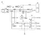
- FIG. 2 is a diagram showing a first embodiment of the switching power supply 100.
- the switching power supply 100 of the present embodiment has the above-mentioned components (in this figure, a switching output circuit 110, an error amplifier 140, a lamp signal generation circuit 150, and so on, as means for realizing the output feedback control of the current mode control method.
- a switching output circuit 110 In addition to the oscillator 160, the PWM comparator 170, and the control circuit 180), it further has a lower current detection unit 210, an information synthesis unit 220, and an information holding unit 230.
- the current output type that outputs the differential current signals IP and IN as the error amplifier 140 that acquires the voltage feedback information Vinyl corresponding to the output voltage VOUT (and the feedback voltage FB).
- An amplifier is used.
- the differential current signals IP and IN are currents that flow in opposite directions to each other, and increase or decrease according to the difference between the feedback voltage FB and the reference voltage REF.
- the larger the difference is, the larger it is in the negative direction ( the direction in which the error amplifier 140 flows).
- the differential current signal IN contrary to the differential current signal IP, increases in the negative direction as the difference between the two increases when REF> FB, and when REF ⁇ FB, both of them The larger the difference, the larger the positive direction.
- the lower current detection unit 210 includes the switch 211 and the resistor 212, detects the inductor current IL (hereinafter referred to as the lower inductor current ILL) flowing through the synchronous rectifier transistor 112, and acquires the current feedback information Iinfo.
- the inductor current IL hereinafter referred to as the lower inductor current ILL
- the second end of the switch 211 is connected to the first end of the resistor 212.
- the switch 211 is turned on / off together with the synchronous rectifier transistor 112 according to the lower gate signal G2. More specifically, the switch 211 turns on during the on period of the synchronous rectifier transistor 112 and turns off during the off period of the synchronous rectifier transistor 112.
- the on-resistance of the transistor 112) is transmitted to the information synthesis unit 220.
- the lower sense signal SNSL is fixed to a zero value via the resistor 212, so that the high level of the switch voltage SW ( ⁇ P VDD) is transmitted to the information synthesis unit 220. There is no such thing.
- any method can be adopted in addition to the method for detecting the drain-source voltage of the synchronous rectifier transistor 112.
- the voltage between both ends of the sense resistor connected in series with the synchronous rectifier transistor 112 may be detected, or the drain-source voltage of the current detection transistor connected in parallel with the synchronous rectifier transistor 112 may be detected. May be good.
- the information synthesis unit 220 includes resistors 221 and 222 (both have a resistance value R), and combines the voltage feedback information Vinyl acquired by the error amplifier 140 with the current feedback information Iinfo acquired by the lower current detection unit 210. Generates synthetic feedback information VIinfo.
- the first term (2IP ⁇ R) on the right side can be understood as the voltage feedback information Vinyl acquired by the error amplifier 140.
- the second term (-ILL ⁇ RonL) on the right side can be understood as the current feedback information Iinfo acquired by the lower current detection unit 210. Therefore, the above difference signal (ERRP-ERRN) can be understood as the combined feedback information VIinfo in which the current feedback information Iinfo is combined with the voltage feedback information Vinfo.
- the information holding unit 230 accepts the differential input of the combined feedback information VIinfo, samples the lower peak value of the inductor current IL during the on period of the synchronous rectifying transistor 112, and differentially holds it during the on period of the output transistor 111.
- a pair of sample / hold circuits 231 and 232 are included to hold and output the signals HLDP and HLDN.
- the sample / hold circuit 231 samples the differential error signal ERRP during the on-period of the synchronous rectifier transistor 112 according to the sample / hold control signal HOLD from the control circuit 180, while differentially holds the differential error signal ERRP during the on-period of the output transistor 111. Hold output the signal HLDP.
- the sample / hold circuit 232 samples the differential error signal ERRN during the on-period of the synchronous rectifier transistor 112 according to the sample / hold control signal HOLD from the control circuit 180, while differentially holds it during the on-period of the output transistor 111. Hold output the signal HLDN.
- the PWM comparator 170 includes a lamp signal RAMP (more accurately, a differential holding signal HLDN to which the lamp signal RAMP is added) input to the inverting input end (-) and a non-inverting input during the ON period of the output transistor 111.
- the off timing of the output transistor 111 is determined by generating an off signal OFF by comparing with the differential holding signal HLDP input to the end (+).
- the output feedback control of the current mode control method can be realized, so that the load response of the output voltage VOUT can be improved.
- the ON period of the output transistor 111 is short. Even in such a case (for example, at the time of high voltage input or low voltage output), it is possible to carry out the output feedback control of the current mode control method without any trouble.
- Information holding units 230 for holding the current feedback information Iinfo are indispensable.
- the information holding unit 230 is provided between the information combining unit 220 and the PWM comparator 170, and holds the combined feedback information VIinfo obtained by synthesizing the current feedback information Iinfo with the voltage feedback information Vinfo.
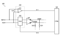
- FIG. 3 is a diagram showing a second embodiment of the switching power supply 100.
- the error correction unit 240 includes a comparator 241 and a digital calibration unit 242.
- the input error detection signal S11 is generated by comparing with the voltage REF.
- the input error detection signal S11 has a high level when FB> REF (that is, Vofs> 0) and a low level when FB ⁇ REF (that is, Vofs ⁇ 0).
- the control circuit 180 generates a digital calibration signal S12 based on the input error detection signal S11 so that the input error Vofs becomes small. For example, when the input error detection signal S11 is at a high level, the digital calibration signal S12 may be generated so as to lower the feedback voltage FB, raise the reference voltage REF, or both. On the contrary, when the input error detection signal S11 is at a low level, the digital calibration signal S12 may be generated so as to raise the feedback voltage FB, lower the reference voltage REF, or both.
- the digital calibration unit 242 corrects at least one of the feedback voltage FB and the reference voltage REF according to the digital calibration signal S12.
- a DAC or the like is preferably used as the digital calibration unit 242 .
- the input error detection signal S11 may be directly input to the digital calibration unit 242, and the digital calibration signal S12 may be generated inside the input error detection signal S11. In that case, the correction process of the input error Vofs can be completed only by the error correction unit 240 without requiring the control circuit 180.
- a general error amplifier has a capacitor for phase compensation (for example, several tens of pF) which is an integrating element, and generates an error signal by charging and discharging the capacitor. Therefore, although oscillation is unlikely to occur, the signal band is limited, which is not suitable for increasing the speed of the voltage feedback control loop. On the other hand, if the integration element is eliminated from the error amplifier, the speed of the voltage feedback control loop can be increased, but on the contrary, it becomes difficult to cancel the input error of the error amplifier.
- phase compensation for example, several tens of pF
- the error amplifier 140 having no integrating element is used to increase the speed of the voltage feedback control loop (several tens of kHz ⁇ several MHz), while the error amplifier is separated from the error amplifier 140.
- An error correction unit 240 for correcting the input error Vofs of 140 has been introduced.
- each design parameter can be separated, so it is possible to achieve both high-speed and high-precision voltage feedback control loops.
- a capacitor for phase compensation is not required, so that it is possible to reduce the chip area and the number of pins.
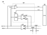
- FIG. 4 is a diagram showing a third embodiment of the switching power supply 100.
- the switching power supply 100 of the present embodiment includes the error correction unit 240 as in the second embodiment (FIG. 3) described above, but its circuit configuration is different.
- the digital calibration unit 246 (for example, DAC) generates a differential input signal from the reference voltage REF to the error correction amplifier 247 in response to the digital calibration signal S12.
- the error correction amplifier 247 generates correction currents IadjP and IadjN according to the differential input signal from the digital calibration unit 246, and adds these to the differential current signals IP and IN of the error amplifier 140.
- the error amplifier 140 has a role as an AC path (high-speed path) for transmitting a change in the output voltage VOUT at high speed. Therefore, the error amplifier 140 is designed without a capacitor and with an emphasis on speed. More simply, it can be said that the error amplifier 140 is faster than the error correction amplifier 247.
- the digital calibration unit 246 and the error correction amplifier 247 have a role as a DC path (low speed path) that determines the accuracy of the output voltage VOUT. Therefore, the error correction amplifier 247 is designed with an emphasis on power saving and accuracy together with the digital calibration unit 246 in the previous stage. More simply, it can be said that the error correction amplifier 247 has higher accuracy than the error amplifier 140.
- FIG. 5 is a diagram showing a fourth embodiment of the switching power supply 100.
- the switching power supply 100 of the present embodiment includes the error correction unit 240 as in the second embodiment (FIG. 3) and the third embodiment (FIG. 4), but the circuit configuration thereof is different.
- the error amplifier 140 is a single output type for the sake of simplicity, but the error amplifier is based on the second embodiment (FIG. 3) and the third embodiment (FIG. 4).
- the 140 may be a differential output type.
- FB ⁇ REF that is, Vofs> 0
- the error correction amplifier 243 is connected in parallel to the error amplifier 140 as a means for correcting the input error Vofs, and its current capacity is suppressed to be sufficiently smaller than the current capacity of the error amplifier 140 (for example, a number). ⁇ A). Further, a capacitor 244 having a small capacity (for example, several pF) is connected to the output end of the error correction amplifier 243. That is, it can be said that the error correction amplifier 243 is a current output type amplifier that has an integrating element and is slower and more accurate than the error amplifier 140.
- the speed and height of the voltage feedback control loop can be increased and increased as in the second and third embodiments. It is possible to achieve both accuracy.
- FIG. 6 is a diagram showing a fifth embodiment of the switching power supply 100.
- the switching power supply 100 of the present embodiment includes the error correction unit 240 as in the second embodiment (FIG. 3), the third embodiment (FIG. 4), and the fourth embodiment (FIG. 5).
- the circuit configuration is different.
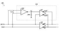
- the error correction unit 240 of the present embodiment is based on the third embodiment (FIG. 4), and replaces the comparator 241 and the digital calibration unit 246 with the fourth embodiment (FIG. 5). ) Includes an error correction amplifier 243 and a capacitor 244.
- the error correction amplifier 243 is a current output type amplifier in which a capacitor 244 having a small capacity (for example, several pF) is connected to its output end.
- the error voltage Vc charged in the capacitor 244 increases when FB ⁇ REF (that is, Vofs> 0) and decreases when FB> REF (that is, Vofs ⁇ 0).
- the error correction amplifier 243 and the capacitor 244 correspond to an integrator that integrates the input error Vofs to generate the error voltage Vc.
- the error correction amplifier 247 generates correction currents IadjP and IadjN according to the difference value between the error voltage Vc input to the non-inverting input end (+) and the reference voltage REF input to the inverting input terminal (-). , Add this to the differential current signals IP and IN of the error amplifier 140.
- the error amplifier 140 has a role as an AC path (high-speed path) for transmitting a change in the output voltage VOUT at high speed. Therefore, the error amplifier 140 is designed without a capacitor and with an emphasis on speed. More simply, it can be said that the error amplifier 140 is faster than the error correction amplifier 247.
- a high speed is used by using an error amplifier 140 having no integrating element. It is important to improve the transient response characteristics when returning from the light load mode by realizing the output feedback control.
- the error voltage Vc cannot be maintained by the above integrator in the light load mode in which the switching operation is temporarily stopped. Therefore, the error correction amplifier 247 may malfunction when returning from the light load mode.
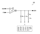
- FIG. 7 is a diagram for explaining the reason why it is difficult to achieve both high speed and high accuracy by using a single error amplifier 140.
- the transconductance of the error amplifier 140 is gm.
- resistors Rc and Cc for phase compensation are generally connected to the output end of the error amplifier 140, and resistors Ro and capacitors Cp are attached as parasitic elements. Therefore, for example, when the transfer function of the error amplifier 140 includes two poles (first pole and second pole) and one zero point, the first pole is determined according to gm, Ro, and Cc, and the second pole is determined. The pole is determined according to gm, Rc and Cp, and the zero point is determined according to gm, Rc and Cc.
- the element size of the error amplifier 140 is increased in order to improve the accuracy of the error amplifier 140, the parasitic capacitor Cp also increases, so that the response speed of the error amplifier 140 decreases.
- the element size of the error amplifier 140 in order to increase the response speed of the error amplifier 140, the element size of the error amplifier 140 must be reduced so that the parasitic capacitor Cp is not attached as much as possible, so that the accuracy of the error amplifier 140 is sacrificed.
- FIG. 8 is a diagram showing a sixth embodiment of the switching power supply 100.
- the switching power supply 100 of the present embodiment has a first signal processing unit (for example, an error amplifier 140a) that forms a first path (DC path / low speed path) instead of a single error amplifier 140 as a component of an output feedback control circuit. ), And a second signal processing unit (for example, an error amplifier 140b) that forms a second path (AC path / high-speed path). That is, in the switching power supply 100 of the present embodiment, the above-mentioned error amplifier 140 is separated into two.
- the transconductances of the error amplifiers 140a and 140b are gm1 and gm2 (however, gm1 ⁇ gm2).
- the error amplifier 140a has a role as a DC path (low speed path) that determines the accuracy of the output voltage VOUT. Therefore, the error amplifier 140a is designed with emphasis on power saving and accuracy (emphasis on high gain and low offset). More simply, it can be said that the error amplifier 140a has higher accuracy than the error amplifier 140b.
- a capacitor Cc for phase compensation is connected to the output end of the error amplifier 140a. Therefore, if Cc >> Cp, the parasitic capacitor Cp can be ignored. Further, a resistor Ro is attached to the output end of the error amplifier 140a as a parasitic element. As a result, the first pole is determined according to gm1, Ro and Cc.
- the error amplifier 140b has a role as an AC path (high-speed path) for transmitting a change in the output voltage VOUT at high speed. Therefore, the error amplifier 140b is designed without a capacitor and with an emphasis on speed. More simply, it can be said that the error amplifier 140b is faster than the error amplifier 140a.
- a resistor Rc for phase compensation is connected to the output end of the error amplifier 140b. Therefore, if Rc ⁇ Ro, the parasitic resistance Ro can be ignored. Further, a capacitor Cp is attached as a parasitic element to the output end of the error amplifier 140b. Conversely, a capacitor other than the parasitic element (for example, a capacitor Cc for phase compensation) is not connected to the output end of the error amplifier 140b. That is, the error amplifier 140b does not have an integrating element. Therefore, the second pole is determined according to gm2, Rc and Cp.
- the transconductance gm1 and gm2 can be arbitrarily set independently of each other. As a result, the adjustment range of the transfer function is widened, so that it is possible to achieve both high speed and high accuracy of the voltage feedback control loop.
- FIG. 9 is a diagram showing a frequency-gain characteristic in the sixth embodiment.
- the low frequency gain can be determined by using the error amplifier 140a that forms a low speed path.
- the transconductance gm1 may be reduced or the capacitance value of the capacitor Cc may be increased.
- the high frequency gain can be determined by using the error amplifier 140b that forms a high-speed path.
- the transconductance gm2 may be increased or the resistance value of the resistor Rc may be increased.
- FIG. 10 is a diagram showing a seventh embodiment of the switching power supply 100.
- the switching power supply 100 of the present embodiment is based on the sixth embodiment (FIG. 8) described above, and is calculated with the buffer 141 in addition to the error amplifiers 140a and 140b, the resistor Rc and the capacitor Cc for phase compensation. Includes a capacitor 142 (adder in the example of this figure).
- the error amplifier 140a outputs an error signal ERR1 according to the difference between the feedback voltage FB input to the inverting input end (-) and the reference voltage REF input to the non-inverting input end (+).
- a digital calibration unit 246 that corrects the input error Vofs may be connected to the input end of the error amplifier 140a. In that case, the capacitor Cc can be omitted.
- the error amplifier 140b outputs an error signal ERR2 according to the difference between the feedback voltage FB input to the inverting input end (-) and the reference voltage REF input to the non-inverting input end (+).
- the buffer 141 is provided between the output end of the error amplifier 140a and the arithmetic unit 142, and outputs the error signal ERR1 generated by the error amplifier 140a to the arithmetic unit 142.
- the arithmetic unit 142 adds the error signals ERR1 and ERR2 to generate an error signal ERR, and outputs this to a PWM comparator 170 (not shown) in the subsequent stage.
- the error amplifier 140a forming the low-speed path and the error amplifier 140b forming the high-speed path are separately prepared, and the error signals ERR1 and ERR2 generated by both are added / subtracted to form the voltage feedback control loop. Both high speed and high accuracy can be achieved.
- FIG. 11 is a diagram showing an eighth embodiment of the switching power supply 100.
- the switching power supply 100 of the present embodiment is based on the sixth embodiment (FIG. 8) described above, and the connection relationship between the error amplifiers 140a and 140b is elaborated.
- the error amplifier 140a outputs an error signal ERR1 according to the difference between the feedback voltage FB input to the inverting input end (-) and the reference voltage REF input to the non-inverting input end (+).
- a digital calibration unit 246 that corrects the input error Vofs may be connected to the input end of the error amplifier 140a. In that case, the capacitor Cc can be omitted.
- the error amplifier 140b generates an error signal ERR2 corresponding to the difference between the feedback voltage FB input to the inverting input end (-) and the error signal ERR1 input to the non-inverting input end (+), and generates an error signal ERR2. It is output as an error signal ERR to the PWM comparator 170 (not shown) in the subsequent stage.
- the switching power supply 100 of the present embodiment achieves both high speed and high accuracy of the voltage feedback control loop without requiring a buffer 141 and an arithmetic unit 142. be able to.
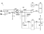
- FIG. 12 is a diagram showing a ninth embodiment of the switching power supply 100.
- the switching power supply 100 of the present embodiment is based on the eighth embodiment (FIG. 11) described above, and has a switching output circuit 110, a PWM comparator 170, a control circuit 180, and lower components as components following the error amplifier 140b.
- the side current detection unit 210, the information synthesis unit 220, and the on-time setting unit 250 are depicted. It should be noted that, with respect to the components already mentioned, basically, the same reference numerals as those in FIGS. 1, 2 and 11 are used to omit duplicated explanations, and in the following, the feature portions of the present embodiment will be focused on in detail. Describe.
- the lower current detection unit 210 detects the lower inductor current ILL flowing through the synchronous rectifier transistor 112 and acquires the current feedback information Iinfo.
- the PWM comparator 170 generates a set signal SET by comparing the differential error signal ERRP input to the non-inverting input end (+) with the differential error signal ERRN input to the inverting input terminal (-). do.
- the on-time setting unit 250 generates a pulse in the reset signal RST when a predetermined on-time elapses from the pulse generation timing of the set signal SET.
- the control circuit 180 sets the switch voltage SW to a high level at the pulse generation timing of the set signal SET, and resets the switch voltage SW to a low level at the pulse generation timing of the reset signal RST.
- the control signal S2 is generated.
- FIG. 13 is a diagram showing an introduction example of the remote sense function.
- the switching power supply 100 of this configuration example is based on FIG. 1 described above, and has an external terminal (remote sense terminal T5) that receives the input of the remote sense signal RSGND from the ground end of the load RL to which the output voltage VOUT is supplied. doing.
- the remote sense signal RSGND may be input to the error amplifier 140, for example (details will be described later).
- the wiring pattern connected to the ground end of the load RL is designed to have low impedance (for example, 10 m ⁇ ).
- a large output current IOUT for example, 1A
- a non-negligible potential fluctuation for example, 10 mV
- the above potential fluctuation corresponds to an output error of 1%.
- the switching power supply 100 of this configuration example accepts the feedback input of the remote sense signal RSGND in order to correct the above potential fluctuation and improve the accuracy of the output voltage VOUT.
- a new embodiment regarding the feedback method of the remote sense signal RSGND will be proposed.
- FIG. 14 is a diagram showing a tenth embodiment of the switching power supply 100.
- the switching power supply 100 of the present embodiment is based on the eighth embodiment (FIG. 11) described above, and further includes an amplifier 143 and an arithmetic unit 144 as means for receiving the feedback input of the remote sense signal RSGND.
- the amplifier 143 amplifies the remote sense signal RSGND and outputs it to the arithmetic unit 144.
- the arithmetic unit 144 superimposes (adds) the remote sense signal RSGND on the feedback voltage FB and outputs it to the error amplifiers 140a and 140b, respectively.
- the output feedback control can be performed so that the fluctuation of the remote sense signal RSGND (and the potential fluctuation at the grounding end of the load RL) is suppressed. Therefore, it is possible to improve the accuracy of the output voltage VOUT.
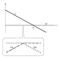
- FIG. 15 is a diagram showing a frequency-gain characteristic in the tenth embodiment.
- the frequency-gain characteristic L1 of the switching power supply 100 (particularly the voltage feedback control loop) is shown by a solid line, and the frequency-gain characteristic L2 required for the amplifier 143 is shown by a broken line.
- the amplifier 143 is required to secure a sufficient band so as not to affect the frequency-gain characteristic L1 of the switching power supply 100. That is, as the response speed of the switching power supply 100 is increased (frequency f1 is shifted to the high frequency side), the amplifier 143 also needs to be increased in speed (frequency f2 is shifted to the high frequency side).
- the response speed can be dramatically increased without sacrificing output accuracy. Therefore, it becomes very difficult to increase the speed of the amplifier 143 in accordance with the improvement in the response speed of the switching power supply 100.
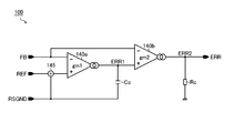
- FIG. 16 is a diagram showing an eleventh embodiment of the switching power supply 100.
- the switching power supply 100 of the present embodiment is based on the eighth embodiment (FIG. 11) described above, and further includes an arithmetic unit 145 as a means for receiving the feedback input of the remote sense signal RSGND.
- the arithmetic unit 145 superimposes (adds) the remote sense signal RSGND on the reference voltage REF instead of the feedback voltage FB and outputs it to the error amplifier 140a.
- FIG. 17 is a diagram showing a frequency-gain characteristic in the eleventh embodiment.
- the frequency-gain characteristic L1 of the switching power supply 100 (particularly the voltage feedback control loop) is shown by a solid line, and the frequency-gain characteristic L3 of the remote sense signal path is shown by a broken line.
- the frequency-gain characteristic L3 of the remote sense signal path includes the frequency-gain characteristic L3a (large broken line) of the first signal path in which the remote sense signal RSGND is superimposed on the reference voltage REF, and the capacitor. It can be understood by decomposing it into the frequency-gain characteristic L3b of the second signal path in which the remote sense signal RSGND is applied to Cc.
- the switching power supply 100 of the present embodiment by combining the above-mentioned first signal path (frequency-gain characteristic L3a) and the second signal path (frequency-gain characteristic L3b), a flat frequency is used in the entire frequency band. -The gain characteristic L3 can be realized. Therefore, even if the high-speed amplifier 143 is not used, the frequency-gain characteristic L1 of the switching power supply 100 is not adversely affected.
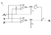
- FIG. 18 is a diagram showing a twelfth embodiment of the switching power supply 100.
- the switching power supply 100 of the present embodiment is based on the seventh embodiment (FIG. 10) described above, and further includes an arithmetic unit 145 as a means for receiving the feedback input of the remote sense signal RSGND.
- the arithmetic unit 145 superimposes (adds) the remote sense signal RSGND on the reference voltage REF and outputs it to the error amplifier 140a.
- the input / output relationship thereof is the same as that of the eleventh embodiment (FIG. 15), and the same effects as those described above can be enjoyed.
- a second embodiment (FIG. 3), a third embodiment (FIG. 4), a fourth embodiment (FIG. 5), a fifth embodiment (FIG. 6), a sixth embodiment (FIG. 8), or a third embodiment. It is also possible to perform the output feedback control of the on-time fixed method illustrated in the ninth embodiment (FIG. 12) by using the error signal ERR generated in the seventh embodiment (FIG. 10).
- the remote sense signal RSGND is input to the input / output of the error correction amplifier 243 in the fourth embodiment (FIG. 5) or the fifth embodiment (FIG. 6). You may. Specifically, the remote sense signal RSGND is superimposed on the reference voltage REF input to the error correction amplifier 243, and the remote sense signal RSGND is applied to one end of the capacitor 244 connected to the output end of the error correction amplifier 243. May be good.
- the switching power supply 100 described so far can be used as a power supply means for various applications.
- the television X in FIG. 19, the personal computer Y in FIG. 20, and the smartphone Z in FIG. 21 can be mentioned.
- the switching power supply 100 can be applied to applications other than those listed here.
- the output feedback control circuit disclosed in the present specification generates a first error signal according to the difference between the output voltage supplied to the load or the feedback voltage corresponding thereto and a predetermined reference voltage.
- a first amplifier a second amplifier that generates a second error signal according to the difference between the output voltage or the feedback voltage and the first error signal or the reference voltage at a speed higher than that of the first amplifier, and the load.
- the arithmetic unit that superimposes the remote sense signal drawn from the ground end on the reference voltage input to the first amplifier is connected between the application end of the first error signal and the application end of the remote sense signal. It has a configuration including a capacitor (first configuration).
- a capacitor other than the parasitic element may not be connected to the output end of the second amplifier (second configuration).
- a resistor may be connected to the output end of the second amplifier (third configuration).
- the first amplifier has a first transconductance
- the second amplifier has a second transconductance different from the first transconductance. (Fourth configuration) may be used.
- the first amplifier is used to determine the low frequency gain
- the second amplifier is used to determine the high frequency gain (first). 5 configuration) may be used.
- the second amplifier uses the second error signal according to the output voltage or the difference between the feedback voltage and the first error signal.
- the second error signal may be output as an error signal (sixth configuration).
- the second amplifier generates the second error signal according to the output voltage or the difference between the feedback voltage and the reference voltage.
- the addition / subtraction signal of the first error signal and the second error signal may be output as an error signal (seventh configuration).
- the switching power supply disclosed in the present specification comprises a switching output circuit that generates an output voltage from an input voltage and supplies it to a load, and the sixth or seventh configuration, and the output voltage or the above.
- the configuration may include a corresponding feedback voltage and an output feedback control circuit that receives an input of a remote sense signal drawn from the ground end of the load and controls the output feedback of the switching output circuit. ..
- the output feedback control circuit may be configured to drive the switching output circuit by a fixed frequency method so that the error signal becomes small (nineth configuration). ..
- the output feedback control circuit may be configured to drive the switching output circuit by a fixed on-time method so that the error signal becomes small (tenth configuration). good.
- the switching power supply in which the output feedback control circuit is incorporated may have a configuration in which the switching frequency fsw is fixed (FIG. 1 or the like) or a configuration in which the switching frequency fsw is variable (FIG. 12 or the like). Further, it does not matter whether the current mode control method or the voltage mode control method is used.
- the output format of the error amplifier may be either single or differential.
- the application target of the output feedback control circuit is not limited to a switching power supply, but may be a power supply of another type, or a servo mechanism other than the power supply.
- the output feedback control circuit disclosed in the present specification is used for a switching power supply or a servo mechanism that needs to perform output feedback control so that the output voltage or the feedback voltage corresponding thereto matches a predetermined reference voltage. It is possible to do.
- Switching power supply 110 Switching output circuit 111 Output transistor (PMOSFET) 112 Synchronous Rectifier Transistor (NMOSFET) 113 inductor 114 capacitor 120 feedback voltage generation circuit 121, 122 resistance 130 reference voltage generation circuit 140, 140a, 140b error amplifier 141 buffer 142 arithmetic unit 143 amplifier 144, 145 arithmetic unit 150 lamp signal generation circuit 160 oscillator 170 PWM comparator 180 control circuit 190 Switch drive circuit 191, 192 driver 200 Semiconductor integrated circuit device (power supply control device) 210 Lower current detector 211 Switch 212 Resistor 220 Information synthesizer 221, 222 Resistance 230 Information holding unit 231, 232 Sample / hold circuit 240 Error correction unit 241 Comparator 242 Digital calibration unit 243 Error correction amplifier 244 Capacitor 245 Resistance 246 Digital calibration Part 247 Error correction amplifier 250 On time setting part Cc, Cp Capacitor Rc, Ro Resistance RL Load T1, T2, T3, T4, T5
Landscapes
- Engineering & Computer Science (AREA)
- Power Engineering (AREA)
- Dc-Dc Converters (AREA)
Abstract
出力帰還制御回路は、例えば、負荷に供給される出力電圧又はこれに応じた帰還電圧FBと所定の基準電圧REFとの差分に応じた第1誤差信号ERR1を生成する第1アンプ140aと、第1アンプ140aよりも高速で出力電圧又は帰還電圧FBと第1誤差信号ERR1(又は基準電圧REF)との差分に応じた第2誤差信号ERR2を生成する第2アンプ140bと、前記負荷の接地端から引き出されるリモートセンス信号RSGNDを第1アンプ140aに入力される基準電圧REFに重畳する演算器145と、第1誤差信号ERR1の印加端とリモートセンス信号RSGNDの印加端との間に接続されたキャパシタCcと、を含む。
Description
本明細書中に開示されている発明は、出力帰還制御回路、及び、これを用いたスイッチング電源に関する。
一般に、スイッチング電源またはサーボ機構などには、出力電圧が所定の基準電圧と一致するように出力帰還制御を行う出力帰還制御回路が組み込まれている。
なお、上記に関連する従来技術の一例としては、特許文献1を挙げることができる。
しかしながら、従来の出力帰還制御回路では、高速化と高精度化の両立について、更なる検討の余地があった。
本明細書中に開示されている発明は、本願の発明者らが見出した上記の課題に鑑み、高速化と高精度化を両立することのできる出力帰還制御回路、及び、これを用いたスイッチング電源を提供することを目的とする。
例えば、本明細書中に開示されている出力帰還制御回路は、負荷に供給される出力電圧又はこれに応じた帰還電圧と所定の基準電圧との差分に応じた第1誤差信号を生成する第1アンプと、前記第1アンプよりも高速で前記出力電圧又は前記帰還電圧と前記第1誤差信号又は前記基準電圧との差分に応じた第2誤差信号を生成する第2アンプと、前記負荷の接地端から引き出されるリモートセンス信号を前記第1アンプに入力される前記基準電圧に重畳する演算器と、前記第1誤差信号の印加端と前記リモートセンス信号の印加端との間に接続されたキャパシタと、を含む。
なお、その他の特徴、要素、ステップ、利点、及び、特性については、以下に続く発明を実施するための形態及びこれに関する添付の図面によって、さらに明らかとなる。
本明細書中に開示されている発明によれば、高速化と高精度化を両立することのできる出力帰還制御回路、及び、これを用いたスイッチング電源を提供することが可能となる。
<スイッチング電源(基本構成)>
図1は、スイッチング電源の基本構成を示す図である。本構成例のスイッチング電源100は、入力電圧PVDDから出力電圧VOUTを生成して不図示の負荷に供給するPWM[pulse width modulation]駆動方式のDC/DCコンバータであり、スイッチング出力回路110と、帰還電圧生成回路120と、基準電圧生成回路130と、エラーアンプ140と、ランプ信号生成回路150と、オシレータ160と、PWMコンパレータ170と、制御回路180と、スイッチ駆動回路190と、を有する。
図1は、スイッチング電源の基本構成を示す図である。本構成例のスイッチング電源100は、入力電圧PVDDから出力電圧VOUTを生成して不図示の負荷に供給するPWM[pulse width modulation]駆動方式のDC/DCコンバータであり、スイッチング出力回路110と、帰還電圧生成回路120と、基準電圧生成回路130と、エラーアンプ140と、ランプ信号生成回路150と、オシレータ160と、PWMコンパレータ170と、制御回路180と、スイッチ駆動回路190と、を有する。
上記の構成要素は、スイッチング出力回路110に含まれる一部の構成要素(本図ではインダクタ113とキャパシタ114)を除き、スイッチング電源100の制御主体となる半導体集積回路装置200(いわゆる電源制御IC)に集積化するとよい。なお、半導体集積回路装置200には、上記以外にも任意の構成要素(各種保護回路など)を適宜組み込むことが可能である。
また、半導体集積回路装置200は、装置外部との電気的な接続を確立するための手段として、複数の外部端子(本図では、電源端子T1、出力端子T2、接地端子T3、並びに、帰還端子T4の4本を例示)を備えている。
スイッチング出力回路110は、ハーフブリッジを形成するように接続された上側スイッチと下側スイッチをオン/オフすることにより、インダクタ電流ILを駆動して入力電圧PVDDから出力電圧VOUTを生成する降圧型のスイッチング出力段であり、出力トランジスタ111と、同期整流トランジスタ112と、インダクタ113と、キャパシタ114と、を含む。
出力トランジスタ111は、スイッチング出力段の上側スイッチとして機能するPMOSFET[P channel type metal oxide semiconductor field effect transistor]である。半導体集積回路装置200の内部において、出力トランジスタ111のソースは、電源端子T1(=入力電圧PVDDの印加端)に接続されている。出力トランジスタ111のドレインは、出力端子T2(=スイッチ電圧SWの印加端)に接続されている。出力トランジスタ111のゲートは、上側ゲート信号G1の印加端に接続されている。出力トランジスタ111は、上側ゲート信号G1がハイレベルであるときにオフし、上側ゲート信号G1がローレベルであるときにオンする。
同期整流トランジスタ112は、スイッチング出力段の下側スイッチとして機能するNMOSFET[N channel type MOSFET]である。半導体集積回路装置200の内部において、同期整流トランジスタ112のソースは、接地端子T3(=接地電圧PVSSの印加端)に接続されている。同期整流トランジスタ112のドレインは、出力端子T2に接続されている。同期整流トランジスタ112のゲートは、下側ゲート信号G2の印加端に接続されている。同期整流トランジスタ112は、下側ゲート信号G2がハイレベルであるときにオンし、下側ゲート信号G2がローレベルであるときにオフする。
インダクタ113とキャパシタ114は、半導体集積回路装置200に外付けされるディスクリート部品であり、スイッチ電圧SWを整流及び平滑して出力電圧VOUTを生成するLCフィルタを形成する。半導体集積回路装置200の外部において、インダクタ113の第1端は、半導体集積回路装置200の出力端子T2に接続されている。インダクタ113の第2端とキャパシタ114の第1端は、出力電圧VOUTの印加端と帰還端子T4に接続されている。キャパシタ114の第2端は、接地端に接続されている。
出力トランジスタ111と同期整流トランジスタ112は、上側ゲート信号G1と下側ゲート信号G2に応じて相補的にオン/オフされる。このようなオン/オフ動作により、インダクタ113の第1端には、入力電圧PVDDと接地電圧GNDとの間でパルス駆動される矩形波状のスイッチ電圧SWが生成される。上記した「相補的」という文言は、出力トランジスタ111と同期整流トランジスタ112のオン/オフ状態が完全に逆転している場合だけでなく、両トランジスタの同時オフ期間(デッドタイム)が設けられている場合も含む。
なお、スイッチング出力回路110の出力形式については、上記の降圧型に限らず、昇圧型、昇降圧型、並びに、反転型のいずれであっても構わない。また、スイッチング出力回路110の整流方式についても、上記の同期整流方式に限らず、下側スイッチとして整流ダイオードを用いたダイオード整流方式を採用してもよい。
また、出力トランジスタ111をNMOSFETに置換することもできる。ただし、その場合には、上側ゲート信号G1のハイレベルを入力電圧PVDDよりも高い電圧値まで引き上げるために、ブートストラップ回路またはチャージポンプ回路が必要となる。
また、出力トランジスタ111及び同期整流トランジスタ112を半導体集積回路装置200に外付けすることも可能である。その場合には、出力端子T2に代えて、上側ゲート信号G1と下側ゲート信号G2をそれぞれ外部出力するための端子が必要となる。
特に、スイッチング出力回路110に対して高電圧が印加される場合には、出力トランジスタ111及び同期整流トランジスタ112として、それぞれ、パワーMOSFET、IGBT[insulated gate bipolar transistor]、若しくは、SiCトランジスタ又はGaNトランジスタなどの高耐圧素子を用いるとよい。
帰還電圧生成回路120は、帰還端子T4(=出力電圧VOUTの印加端)と接地端との間に直列接続された抵抗121及び122を含み、両抵抗間の接続ノードから出力電圧VOUTに応じた帰還電圧FB(=出力電圧VOUTの分圧電圧)を出力する。
なお、出力電圧VOUTがエラーアンプ140の入力ダイナミックレンジ内に収まっている場合には、帰還電圧生成回路120を省略して出力電圧VOUTをエラーアンプ140に直接入力しても構わない。また、抵抗121と並列にキャパシタを接続してもよい。
また、抵抗121及び122を半導体集積回路装置200に外付けすることもできる。その場合、抵抗121及び122相互間の接続ノードを帰還端子T4に接続すればよい。
基準電圧生成回路130は、所定の基準電圧REF(=出力電圧VOUTの目標設定値に相当)を生成する。なお、基準電圧生成回路130としては、デジタルの基準電圧設定信号をアナログの基準電圧REFに変換するDAC[digital-to-analog converter]を用いるとよい。このような構成であれば、上記の基準電圧設定信号を用いて、起動時のソフトスタート動作を実現したり、出力電圧VOUTを調整したりすることが可能となる。
エラーアンプ140は、反転入力端(-)に印加される帰還電圧FBと、非反転入力端(+)に印加される基準電圧REFとの差分に応じた誤差信号ERRを生成する。誤差信号ERRは、帰還電圧FBが基準電圧REFよりも低いときに上昇し、帰還電圧FBが基準電圧REFよりも高いときに低下する。
ランプ信号生成回路150は、出力トランジスタ111のオン期間Tonに上昇する三角波状、鋸波状、若しくは、n次スロープ波状(例えばn=2)のランプ信号RAMPを生成する。なお、ランプ信号RAMPは、例えば、出力トランジスタ111のオンタイミングでゼロ値から上昇を開始し、出力トランジスタ111のオフタイミングでゼロ値にリセットされる。
オシレータ160は、所定のスイッチング周波数fsw(=1/Tsw)でパルス駆動されるオン信号ON(=クロック信号)を生成する。
PWMコンパレータ170は、非反転入力端(+)に印加される誤差信号ERRと、反転入力端(-)に印加されるランプ信号RAMPを比較してオフ信号OFFを生成する。なお、オフ信号OFFは、ランプ信号RAMPが誤差信号ERRよりも低いときにハイレベルとなり、ランプ信号RAMPが誤差信号ERRよりも高いときにローレベルとなる。すなわち、オフ信号OFFのパルス生成タイミングは、誤差信号ERRが高いほど遅くなり、誤差信号ERRが低いほど早くなる。
制御回路180は、オン信号ONとオフ信号OFFに応じて上側制御信号S1と下側制御信号S2を生成する。具体的に述べると、制御回路180は、オン信号ONにパルスが生成されたときに、上側制御信号S1と下側制御信号S2をいずれもローレベル(=スイッチ電圧SWをハイレベルとするときの論理レベル)に立ち下げる一方、オフ信号OFFにパルスが生成されたときに、上側制御信号S1と下側制御信号S2をいずれもハイレベル(=スイッチ電圧SWをローレベルとするときの論理レベル)に立ち上げる。
従って、出力トランジスタ111のオン期間Ton(=スイッチ電圧SWのハイレベル期間)は、オフ信号OFFのパルス生成タイミングが遅いほど長くなり、逆に、オフ信号OFFのパルス生成タイミングが早いほど短くなる。すなわち、出力トランジスタ111のオンデューティD(=Ton/Tsw)は、誤差信号ERRが高いほど大きくなり、誤差信号ERRが低いほど小さくなる。
スイッチ駆動回路190は、上側制御信号S1の入力を受け付けて上側ゲート信号G1を生成する上側ドライバ191と、下側制御信号S2の入力を受け付けて下側ゲート信号G2を生成する下側ドライバ192を含む。上側ドライバ191及び192としては、それぞれ、バッファまたはインバータを用いることができる。
なお、上記構成要素のうち、少なくとも、エラーアンプ140、ランプ信号生成回路150、オシレータ160、PWMコンパレータ170、制御回路180、及び、スイッチ駆動回路190は、帰還電圧FB(延いては出力電圧VOUT)が所定の基準電圧REFと一致するように出力帰還制御を行う出力帰還制御回路として理解することができる。
特に、上記の出力帰還制御回路では、誤差信号ERRが小さくなるように周波数固定方式でスイッチング出力回路110が駆動されることになる。
<第1実施形態>
図2は、スイッチング電源100の第1実施形態を示す図である。本実施形態のスイッチング電源100は、電流モード制御方式の出力帰還制御を実現するための手段として、先出の構成要素(本図では、スイッチング出力回路110、エラーアンプ140、ランプ信号生成回路150、オシレータ160、PWMコンパレータ170、及び、制御回路180を明示)に加えて、下側電流検出部210と、情報合成部220と、情報保持部230をさらに有する。
図2は、スイッチング電源100の第1実施形態を示す図である。本実施形態のスイッチング電源100は、電流モード制御方式の出力帰還制御を実現するための手段として、先出の構成要素(本図では、スイッチング出力回路110、エラーアンプ140、ランプ信号生成回路150、オシレータ160、PWMコンパレータ170、及び、制御回路180を明示)に加えて、下側電流検出部210と、情報合成部220と、情報保持部230をさらに有する。
なお、本実施形態のスイッチング電源100では、出力電圧VOUT(延いては帰還電圧FB)に応じた電圧帰還情報Vinfoを取得するエラーアンプ140として、差動電流信号IP及びINを出力する電流出力型アンプが用いられている。差動電流信号IP及びINは、互いに逆向きに流れる電流であり、帰還電圧FBと基準電圧REFとの差分に応じて増減する。
より具体的に述べると、差動電流信号IPは、REF>FBであるときには、両者の差分が大きいほど正方向(=エラーアンプ140から流れ出る方向)に大きくなり、REF<FBであるときには、両者の差分が大きいほど負方向(=エラーアンプ140に流れ込む方向)に大きくなる。
これに対して、差動電流信号INは、差動電流信号IPとは逆に、REF>FBであるときには、両者の差分が大きいほど負方向に大きくなり、REF<FBであるときには、両者の差分が大きいほど正方向に大きくなる。
下側電流検出部210は、スイッチ211と抵抗212を含み、同期整流トランジスタ112に流れるインダクタ電流IL(以下では下側インダクタ電流ILLと呼ぶ)を検出して電流帰還情報Iinfoを取得する。
スイッチ211の第1端は、同期整流トランジスタ112のドレイン(=スイッチ電圧SWの印加端)に接続されている。スイッチ211の第2端は、抵抗212の第1端に接続されている。抵抗212の第2端は、同期整流トランジスタ112のソース(=接地電圧PVSSの印加端)に接続されている。
なお、スイッチ211は、下側ゲート信号G2に応じて同期整流トランジスタ112と共にオン/オフされる。より具体的に述べると、スイッチ211は、同期整流トランジスタ112のオン期間にオンし、同期整流トランジスタ112のオフ期間にオフする。
従って、同期整流トランジスタ112のオン期間には、先述の電流帰還情報Iinfoとして、下側インダクタ電流ILLに応じた下側センス信号SNSL(=SW-PVSS=-ILL×RonL、ただし、RonLは同期整流トランジスタ112のオン抵抗)が情報合成部220に伝達される。一方、同期整流トランジスタ112のオフ期間には、下側センス信号SNSLが抵抗212を介してゼロ値に固定されるので、スイッチ電圧SWのハイレベル(≒PVDD)が情報合成部220に伝達されることはない。
なお、下側インダクタ電流ILLの検出手法については、同期整流トランジスタ112のドレイン・ソース間電圧を検出する手法のほかにも、任意の手法を採用することが可能である。例えば、同期整流トランジスタ112に直列接続されたセンス抵抗の両端間電圧を検出してもよいし、或いは、同期整流トランジスタ112に並列接続された電流検出用トランジスタのドレイン・ソース間電圧を検出してもよい。
情報合成部220は、抵抗221及び222(いずれも抵抗値R)を含み、エラーアンプ140で取得された電圧帰還情報Vinfoに下側電流検出部210で取得された電流帰還情報Iinfoを合成して合成帰還情報VIinfoを生成する。
抵抗221の第1端は、エラーアンプ140の第1出力端(=差動電流信号IPの出力端)に接続されている。抵抗221の第2端は、下側電流検出部210の第1出力端(=下側センス信号SNSLの出力端)に接続されている。
抵抗222の第1端は、エラーアンプ140の第2出力端(=差動電流信号INの出力端)に接続されている。抵抗222の第2端は、下側電流検出部210の第2出力端(=接地電圧PVSSの印加端)に接続されている。
なお、抵抗221の第1端から出力される正側の差動誤差信号(電圧信号)は、ERRP=IP×R+SWと表すことができる。また、抵抗222の第1端から出力される負側の差動誤差信号(電圧信号)は、ERRN=IN×R+PVSS(ただしIN=-IP)と表すことができる。
従って、差動誤差信号ERRP及びERRNの差分信号は、ERRP-ERRN=2IP×R-ILL×RonLと表される。ここで、右辺第1項(2IP×R)は、エラーアンプ140で取得された電圧帰還情報Vinfoとして理解することができる。また、右辺第2項(-ILL×RonL)は、下側電流検出部210で取得された電流帰還情報Iinfoとして理解することができる。従って、上記の差分信号(ERRP-ERRN)は、電圧帰還情報Vinfoに電流帰還情報Iinfoを合成した合成帰還情報VIinfoとして理解することができる。
情報保持部230は、合成帰還情報VIinfoの差動入力を受け付けており、同期整流トランジスタ112のオン期間にインダクタ電流ILの下側ピーク値をサンプリングするとともに、出力トランジスタ111のオン期間に差動保持信号HLDP及びHLDNをホールド出力するために、一対のサンプル/ホールド回路231及び232を含む。
サンプル/ホールド回路231は、制御回路180からのサンプル/ホールド制御信号HOLDに応じて、同期整流トランジスタ112のオン期間に差動誤差信号ERRPをサンプリングする一方、出力トランジスタ111のオン期間に差動保持信号HLDPをホールド出力する。
サンプル/ホールド回路232は、制御回路180からのサンプル/ホールド制御信号HOLDに応じて、同期整流トランジスタ112のオン期間に差動誤差信号ERRNをサンプリングする一方、出力トランジスタ111のオン期間に差動保持信号HLDNをホールド出力する。
PWMコンパレータ170は、出力トランジスタ111のオン期間において、反転入力端(-)に入力されるランプ信号RAMP(より正確には、ランプ信号RAMPが足し合わされた差動保持信号HLDN)と、非反転入力端(+)に入力される差動保持信号HLDPとを比較してオフ信号OFFを生成することにより、出力トランジスタ111のオフタイミングを決定する。
本実施形態のスイッチング電源100であれば、電流モード制御方式の出力帰還制御を実現することができるので、出力電圧VOUTの負荷応答性を高めることが可能となる。
特に、出力トランジスタ111に流れるインダクタ電流IL(以下では上側インダクタ電流ILHと呼ぶ)ではなく、同期整流トランジスタ112に流れる下側インダクタ電流ILLを検出する構成であれば、出力トランジスタ111のオン期間が短くなる場合(例えば高電圧入力時または低電圧出力時)であっても、電流モード制御方式の出力帰還制御を支障なく実施することが可能となる。
なお、下側インダクタ電流ILLに応じた電流帰還情報Iinfoを用いて電流モード制御方式の出力帰還制御を行うためには、同期整流トランジスタ112のオン期間(=出力トランジスタ111のオフ期間)に取得された電流帰還情報Iinfoを保持しておくための情報保持部230(サンプル/ホールド回路231及び232)が必須となる。
ここで、情報保持部230は、情報合成部220とPWMコンパレータ170との間に設けられており、電圧帰還情報Vinfoに電流帰還情報Iinfoを合成して得られた合成帰還情報VIinfoを保持する。
このような構成であれば、情報保持部230のホールド出力期間において、情報保持部230の前段にノイズが重畳しても、PWMコンパレータ170での信号比較処理には、何ら影響が及ばない。従って、安定したデューティ制御を実現することが可能となる。
また、電圧帰還情報Vinfoと電流帰還情報Iinfoを加算後にサンプル/ホールドすることにより、電圧帰還情報Vinfoと電流帰還情報Iinfoとの間の時間的な齟齬を防止し、スイッチング電源100の性能を向上することが可能となる。
<第2実施形態>
図3は、スイッチング電源100の第2実施形態を示す図である。本実施形態のスイッチング電源100は、先出の基本構成(図1)または第1実施形態(図2)を基本としつつ、積分要素(寄生素子を除く)を持たないエラーアンプ140の入力誤差Vofs(=FB-REF)を検出してエラーアンプ140の入力信号(=帰還電圧FBと基準電圧REFの少なくとも一方)を補正する誤差補正部240をさらに有する。なお、誤差補正部240は、コンパレータ241とデジタル較正部242を含む。
図3は、スイッチング電源100の第2実施形態を示す図である。本実施形態のスイッチング電源100は、先出の基本構成(図1)または第1実施形態(図2)を基本としつつ、積分要素(寄生素子を除く)を持たないエラーアンプ140の入力誤差Vofs(=FB-REF)を検出してエラーアンプ140の入力信号(=帰還電圧FBと基準電圧REFの少なくとも一方)を補正する誤差補正部240をさらに有する。なお、誤差補正部240は、コンパレータ241とデジタル較正部242を含む。
コンパレータ241は、エラーアンプ140の入力誤差Vofs(=FB-REF)を検出する手段であり、非反転入力端(+)に入力される帰還電圧FBと反転入力端(-)に入力される基準電圧REFとを比較して入力誤差検出信号S11を生成する。なお、入力誤差検出信号S11は、FB>REF(すなわちVofs>0)であるときにハイレベルとなり、FB<REF(すなわちVofs<0)であるときにローレベルとなる。
制御回路180は、入力誤差検出信号S11に基づいて、入力誤差Vofsが小さくなるように、デジタル較正信号S12を生成する。例えば、入力誤差検出信号S11がハイレベルであるときには、帰還電圧FBを引き下げるか、基準電圧REFを引き上げるか、若しくは、その両方を行うように、デジタル較正信号S12を生成すればよい。逆に、入力誤差検出信号S11がローレベルであるときには、帰還電圧FBを引き上げるか、基準電圧REFを引き下げるか、若しくは、その両方を行うように、デジタル較正信号S12を生成すればよい。
デジタル較正部242は、デジタル較正信号S12に応じて、帰還電圧FB及び基準電圧REFの少なくとも一方を補正する。なお、デジタル較正部242としては、DACなどが好適に用いられる。また、入力誤差検出信号S11をデジタル較正部242に直接入力し、その内部でデジタル較正信号S12を生成する構成としてもよい。その場合には、制御回路180を要することなく、誤差補正部240だけで入力誤差Vofsの補正処理を完結することができる。
次に、誤差補正部240の導入意義について詳細に説明する。
一般的なエラーアンプは、積分要素となる位相補償用のキャパシタ(例えば数十pF)を持ち、その充放電を行うことで誤差信号を生成する。そのため、発振を生じ難い反面、信号帯域に制限が掛かるので、電圧帰還制御ループの高速化には不向きである。一方、エラーアンプから積分要素を排除すると、電圧帰還制御ループの高速化を実現できるが、背反として、エラーアンプの入力誤差をキャンセルし難くなる。
そこで、本実施形態のスイッチング電源100では、積分要素を持たないエラーアンプ140を用いて電圧帰還制御ループの高速化(数十kHz→数MHz)を図る一方、エラーアンプ140とは別に、エラーアンプ140の入力誤差Vofsを補正するための誤差補正部240が導入されている。
このように、高速電圧帰還と誤差補正を並列化することにより、それぞれの設計パラメータを分離することができるので、電圧帰還制御ループの高速化と高精度化を両立することが可能となる。また、一般的なエラーアンプと異なり、位相補償用のキャパシタを必要としないので、チップ面積の縮小及びピン数の削減を図ることも可能となる。
<第3実施形態>
図4は、スイッチング電源100の第3実施形態を示す図である。本実施形態のスイッチング電源100は、先出の第2実施形態(図3)と同じく、誤差補正部240を備えているが、その回路構成が異なっている。
図4は、スイッチング電源100の第3実施形態を示す図である。本実施形態のスイッチング電源100は、先出の第2実施形態(図3)と同じく、誤差補正部240を備えているが、その回路構成が異なっている。
より具体的に述べると、本実施形態の誤差補正部240は、先出のコンパレータ241と共に、デジタル較正部246と誤差補正アンプ247を含み、エラーアンプ140の入力誤差Vofsを検出してエラーアンプ140の出力信号(=差動誤差信号ERRP及びERRN)を補正する。
デジタル較正部246(例えばDAC)は、デジタル較正信号S12に応じて、基準電圧REFから誤差補正アンプ247への差動入力信号を生成する。
誤差補正アンプ247は、デジタル較正部246からの差動入力信号に応じた補正電流IadjP及びIadjNを生成し、これをエラーアンプ140の差動電流信号IP及びINに足し合わせる。
なお、エラーアンプ140は、出力電圧VOUTの変化を高速に伝達するACパス(高速パス)としての役割を持つ。そのため、エラーアンプ140は、コンデンサレスかつスピード重視で設計されている。より端的に述べると、エラーアンプ140は、誤差補正アンプ247よりも高速であると言える。
一方、デジタル較正部246と誤差補正アンプ247は、出力電圧VOUTの精度を決定するDCパス(低速パス)としての役割を持つ。そのため、誤差補正アンプ247は、前段のデジタル較正部246と共に、省電力かつ精度重視で設計されている。より端的に述べると、誤差補正アンプ247は、エラーアンプ140よりも高精度であると言える。
このように、エラーアンプ140の入力信号を補正するのではなく、エラーアンプ140の出力信号を補正する構成であっても、電圧帰還制御ループの高速化と高精度化を両立することが可能である。
<第4実施形態>
図5は、スイッチング電源100の第4実施形態を示す図である。本実施形態のスイッチング電源100は、先の第2実施形態(図3)及び第3実施形態(図4)と同じく、誤差補正部240を備えているが、その回路構成が異なっている。
図5は、スイッチング電源100の第4実施形態を示す図である。本実施形態のスイッチング電源100は、先の第2実施形態(図3)及び第3実施形態(図4)と同じく、誤差補正部240を備えているが、その回路構成が異なっている。
より具体的に述べると、本実施形態の誤差補正部240は、誤差補正アンプ243と、キャパシタ244と、抵抗245を含み、エラーアンプ140の入力誤差Vofsを検出して補正電流Iadj(=第1誤差信号に相当)を生成し、これを用いてエラーアンプ140から出力される誤差信号ERR0(=第2誤差信号に相当)を補正する。
なお、本実施形態では、説明を簡単とするために、エラーアンプ140をシングル出力型としているが、先の第2実施形態(図3)及び第3実施形態(図4)に倣い、エラーアンプ140を差動出力型としても構わない。
誤差補正アンプ243は、反転入力端(-)に印加される帰還電圧FBと非反転入力端(+)に印加される基準電圧REFとの差分(=入力誤差Vofs)に応じた補正電流Iadjを生成する。なお、FB<REF(すなわちVofs>0)であるときには、両者の差分が大きいほど補正電流Iadjが正方向(=誤差補正アンプ243の出力端から抵抗245を介してエラーアンプ140の出力端に向かう方向)に大きくなる。一方、FB>REF(すなわちVofs<0)であるときには、両者の差分が大きいほど補正電流Iadjが負方向(=エラーアンプ140の出力端から抵抗245を介して誤差補正アンプ243の出力端に向かう方向)に大きくなる。
ただし、誤差補正アンプ243は、あくまで、入力誤差Vofsの補正手段としてエラーアンプ140に並列接続されており、その電流能力は、エラーアンプ140の電流能力よりも十分に小さく抑えられている(例えば数μA)。また、誤差補正アンプ243の出力端には、小容量(例えば数pF)のキャパシタ244が接続されている。すなわち、誤差補正アンプ243は、積分要素を持ち、エラーアンプ140よりも低速かつ高精度な電流出力型アンプであると言える。
抵抗245(抵抗値:Radj)は、エラーアンプ140の出力端と誤差補正アンプ243の出力端との間に接続されており、その両端間電圧を補正電圧Vadj(=Iadj×Radj)として誤差信号ERRに足し合わせることにより、補正済みの誤差信号ERR(=ERR0+Vadj)を生成するための加算器として機能する。
例えば、FB<REFであるときには、正方向の補正電流Iadjが流れるので、誤差信号ERR0が補正電圧Vadjだけ引き上げられる。その結果、補正済みの誤差信号ERRが上昇した分だけ、出力トランジスタ111のオフタイミングが遅れるので、出力電圧VOUT(延いては帰還電圧FB)が上昇し、入力誤差Vofsが減少する。
一方、FB>REFであるときには、負方向の補正電流Iadjが流れるので、誤差信号ERR0が補正電圧Vadjだけ引き下げられる。その結果、補正済みの誤差信号ERRが低下した分だけ、出力トランジスタ111のオフタイミングが早まるので、出力電圧VOUT(延いては帰還電圧FB)が低下し、入力誤差Vofsが減少する。
このように、エラーアンプ140に対して低速かつ高精度な誤差補正アンプ243を並列に接続することにより、先の第2実施形態及び第3実施形態と同じく、電圧帰還制御ループの高速化と高精度化を両立することが可能となる。
<第5実施形態>
図6は、スイッチング電源100の第5実施形態を示す図である。本実施形態のスイッチング電源100は、先の第2実施形態(図3)、第3実施形態(図4)、第4実施形態(図5)と同じく、誤差補正部240を備えているが、その回路構成が異なっている。
図6は、スイッチング電源100の第5実施形態を示す図である。本実施形態のスイッチング電源100は、先の第2実施形態(図3)、第3実施形態(図4)、第4実施形態(図5)と同じく、誤差補正部240を備えているが、その回路構成が異なっている。
より具体的に述べると、本実施形態の誤差補正部240は、先の第3実施形態(図4)を基本としつつ、コンパレータ241及びデジタル較正部246に代えて、第4実施形態(図5)の誤差補正アンプ243及びキャパシタ244を含む。
誤差補正アンプ243は、その出力端に小容量(例えば数pF)のキャパシタ244が接続された電流出力型アンプである。なお、キャパシタ244に充電された誤差電圧Vcは、FB<REF(すなわちVofs>0)であるときに上昇し、FB>REF(すなわちVofs<0)であるときに低下する。このように、誤差補正アンプ243及びキャパシタ244は、入力誤差Vofsを積分して誤差電圧Vcを生成する積分器に相当する。
誤差補正アンプ247は、非反転入力端(+)に入力される誤差電圧Vcと、反転入力端(-)に入力される基準電圧REFとの差分値に応じた補正電流IadjP及びIadjNを生成し、これをエラーアンプ140の差動電流信号IP及びINに足し合わせる。
なお、エラーアンプ140は、先にも述べたように、出力電圧VOUTの変化を高速に伝達するACパス(高速パス)としての役割を持つ。そのため、エラーアンプ140は、コンデンサレスかつスピード重視で設計されている。より端的に述べると、エラーアンプ140は、誤差補正アンプ247よりも高速であると言える。
一方、誤差補正アンプ247とその前段に接続される積分器(=誤差補正アンプ243及びキャパシタ244)は、出力電圧VOUTの精度を決定するDCパス(低速パス)としての役割を持つ。そのため、誤差補正アンプ247は、その前段の積分器と共に、省電力かつ精度重視で設計されている。より端的に述べると、誤差補正アンプ247は、エラーアンプ140よりも高精度であると言える。
本構成を採用することにより、先の第2実施形態、第3実施形態、ないしは、第4実施形態と同じく、電圧帰還制御ループの高速化と高精度化を両立することが可能となる。
特に、スイッチング電源100に軽負荷モード(=軽負荷時にスイッチング動作を一時停止して消費電力を低減する省電力モード)が実装される場合には、積分要素を持たないエラーアンプ140を用いて高速な出力帰還制御を実現することにより、軽負荷モードからの復帰時における過渡応答特性を高めておくことが重要となる。
ただし、本実施形態のスイッチング電源100では、スイッチング動作が一時停止される軽負荷モードにおいて、上記の積分器で誤差電圧Vcを保持しておくことができない。そのため、軽負荷モードからの復帰時に誤差補正アンプ247が誤動作を生じ得る。
このような不具合を回避するためには、例えば、軽負荷モードでも誤差電圧Vcが所定の下限値を下回らないように制限するクランパ(不図示)を積分器の後段に設けておくとよい。また、もちろん、先の第2実施形態(図3)及び第3実施形態(図4)を採用し、デジタル較正部246を用いて電圧情報を保持してもよい。
<高速化と高精度化の両立>
図7は、単一のエラーアンプ140を用いて高速化と高精度化を両立することが難しい理由を説明するための図である。なお、以下では、エラーアンプ140のトランスコンダクタンスがgmであるものとして説明する。
図7は、単一のエラーアンプ140を用いて高速化と高精度化を両立することが難しい理由を説明するための図である。なお、以下では、エラーアンプ140のトランスコンダクタンスがgmであるものとして説明する。
本図で示したように、エラーアンプ140の出力端には、一般に、位相補償用の抵抗Rc及びCcが接続されているほか、寄生素子として抵抗Ro及びキャパシタCpが付随している。そのため、例えば、エラーアンプ140の伝達関数が2つの極(第1ポールと第2ポール)と1つのゼロ点を含む場合には、第1ポールがgm、Ro及びCcに応じて決まり、第2ポールがgm、Rc及びCpに応じて決まり、ゼロ点がgm、Rc及びCcに応じて決まる。
このように、2つの極と1つのゼロ点は、それぞれの関係が独立していない。また、半導体集積回路装置200では、内部パラメータ(gm、Rc、Ccなど)の設定値に制約がある。そのため、単一のエラーアンプ140を用いて2つの極と1つのゼロ点を狙い通りに設定することは困難である。
例えば、エラーアンプ140の精度を高めるために、エラーアンプ140の素子サイズを大型化すると、寄生のキャパシタCpも大きくなるので、エラーアンプ140の応答速度が低下してしまう。一方、エラーアンプ140の応答速度を高めるためには、できるだけ寄生のキャパシタCpが付随しないように、エラーアンプ140の素子サイズを小型化しなければならないので、エラーアンプ140の精度が犠牲となる。
以下では、上記の考察に鑑み、高速化と高精度化を両立することのできる出力帰還制御回路について提案する。
<第6実施形態>
図8は、スイッチング電源100の第6実施形態を示す図である。本実施形態のスイッチング電源100は、出力帰還制御回路の構成要素として、単一のエラーアンプ140ではなく、第1経路(DCパス/低速パス)を形成する第1信号処理部(例えばエラーアンプ140a)と、第2経路(ACパス/高速パス)を形成する第2信号処理部(例えばエラーアンプ140b)と、を有する。すなわち、本実施形態のスイッチング電源100では、先出のエラーアンプ140が2つに分離されている。なお、以下では、エラーアンプ140a及び140bそれぞれのトランスコンダクタンスがgm1及びgm2(ただしgm1≠gm2)であるものとして説明する。
図8は、スイッチング電源100の第6実施形態を示す図である。本実施形態のスイッチング電源100は、出力帰還制御回路の構成要素として、単一のエラーアンプ140ではなく、第1経路(DCパス/低速パス)を形成する第1信号処理部(例えばエラーアンプ140a)と、第2経路(ACパス/高速パス)を形成する第2信号処理部(例えばエラーアンプ140b)と、を有する。すなわち、本実施形態のスイッチング電源100では、先出のエラーアンプ140が2つに分離されている。なお、以下では、エラーアンプ140a及び140bそれぞれのトランスコンダクタンスがgm1及びgm2(ただしgm1≠gm2)であるものとして説明する。
エラーアンプ140aは、出力電圧VOUTの精度を決定するDCパス(低速パス)としての役割を持つ。そのため、エラーアンプ140aは、省電力かつ精度重視(高ゲインかつ低オフセット重視)で設計されている。より端的に述べると、エラーアンプ140aは、エラーアンプ140bよりも高精度であると言える。
なお、エラーアンプ140aの出力端には、位相補償用のキャパシタCcが接続されている。従って、Cc>>Cpであれば、寄生のキャパシタCpを無視することができる。また、エラーアンプ140aの出力端には、寄生素子として抵抗Roが付随している。その結果、第1ポールがgm1、Ro及びCcに応じて決まる。
これに対して、エラーアンプ140bは、出力電圧VOUTの変化を高速に伝達するACパス(高速パス)としての役割を持つ。そのため、エラーアンプ140bは、コンデンサレスかつスピード重視で設計されている。より端的に述べると、エラーアンプ140bは、エラーアンプ140aよりも高速であると言える。
なお、エラーアンプ140bの出力端には、位相補償用の抵抗Rcが接続されている。従って、Rc<<Roであれば、寄生の抵抗Roを無視することができる。また、エラーアンプ140bの出力端には、寄生素子としてキャパシタCpが付随している。逆に言うと、エラーアンプ140bの出力端には、寄生素子以外のキャパシタ(例えば、位相補償用のキャパシタCc)が接続されていない。すなわち、エラーアンプ140bは、積分要素を持たない。従って、第2ポールがgm2、Rc及びCpに応じて決まる。
このように、低速パスを形成するエラーアンプ140aと、高速パスを形成するエラーアンプ140bを個別に用意することにより、それぞれのトランスコンダクタンスgm1及びgm2を互いに独立して任意に設定することができる。その結果、伝達関数の調整範囲が広がるので、電圧帰還制御ループの高速化と高精度化を両立することが可能となる。
図9は、第6実施形態における周波数-ゲイン特性を示す図である。本図で示したように、低域ゲインは、低速パスを形成するエラーアンプ140aを用いて決定することができる。例えば、低域ゲインを引き上げるためには、トランスコンダクタンスgm1を小さくしたり、キャパシタCcの容量値を大きくしたりすればよい。
一方、高域ゲインは、高速パスを形成するエラーアンプ140bを用いて決定することができる。例えば、高域ゲインを引き上げるためには、トランスコンダクタンスgm2を大きくしたり、抵抗Rcの抵抗値を高くしたりすればよい。
<第7実施形態>
図10は、スイッチング電源100の第7実施形態を示す図である。本実施形態のスイッチング電源100は、先出の第6実施形態(図8)を基本としつつ、エラーアンプ140a及び140b、並びに、位相補償用の抵抗Rc及びキャパシタCcに加えて、バッファ141と演算器142(本図の例では加算器)を含む。
図10は、スイッチング電源100の第7実施形態を示す図である。本実施形態のスイッチング電源100は、先出の第6実施形態(図8)を基本としつつ、エラーアンプ140a及び140b、並びに、位相補償用の抵抗Rc及びキャパシタCcに加えて、バッファ141と演算器142(本図の例では加算器)を含む。
エラーアンプ140aは、反転入力端(-)に入力される帰還電圧FBと、非反転入力端(+)に入力される基準電圧REFとの差分に応じた誤差信号ERR1を出力する。なお、先出の第3実施形態(図4)に倣い、エラーアンプ140aの入力端には、入力誤差Vofsを補正するデジタル較正部246を接続してもよい。その場合、キャパシタCcは省略することも可能である。
エラーアンプ140bは、反転入力端(-)に入力される帰還電圧FBと、非反転入力端(+)に入力される基準電圧REFとの差分に応じた誤差信号ERR2を出力する。
バッファ141は、エラーアンプ140aの出力端と演算器142との間に設けられており、エラーアンプ140aで生成された誤差信号ERR1を演算器142に出力する。
演算器142は、誤差信号ERR1及びERR2を足し合わせて誤差信号ERRを生成し、これを後段のPWMコンパレータ170(不図示)に出力する。
このように、低速パスを形成するエラーアンプ140aと、高速パスを形成するエラーアンプ140bを個別に用意し、双方で生成される誤差信号ERR1及びERR2の加減算を行うことにより、電圧帰還制御ループの高速化と高精度化を両立することができる。
<第8実施形態>
図11は、スイッチング電源100の第8実施形態を示す図である。本実施形態のスイッチング電源100は、先出の第6実施形態(図8)を基本としつつ、エラーアンプ140a及び140b相互間の接続関係に工夫が凝らされている。
図11は、スイッチング電源100の第8実施形態を示す図である。本実施形態のスイッチング電源100は、先出の第6実施形態(図8)を基本としつつ、エラーアンプ140a及び140b相互間の接続関係に工夫が凝らされている。
エラーアンプ140aは、反転入力端(-)に入力される帰還電圧FBと、非反転入力端(+)に入力される基準電圧REFとの差分に応じた誤差信号ERR1を出力する。なお、先出の第3実施形態(図4)に倣い、エラーアンプ140aの入力端には、入力誤差Vofsを補正するデジタル較正部246を接続してもよい。その場合、キャパシタCcは省略することも可能である。
エラーアンプ140bは、反転入力端(-)に入力される帰還電圧FBと、非反転入力端(+)に入力される誤差信号ERR1との差分に応じた誤差信号ERR2を生成して、これを誤差信号ERRとして後段のPWMコンパレータ170(不図示)に出力する。
本実施形態のスイッチング電源100であれば、先出の第7実施形態(図10)と異なり、バッファ141及び演算器142を要することなく、電圧帰還制御ループの高速化と高精度化を両立することができる。
なお、改めて図示はしないが、帰還電圧FB及び基準電圧REFそれぞれの入力端を互いに入れ替えるとともに、エラーアンプ140bの入力極性を正負反転させても、上記と同様の作用効果を享受することが可能である。
<第9実施形態>
図12は、スイッチング電源100の第9実施形態を示す図である。本実施形態のスイッチング電源100は、先出の第8実施形態(図11)を基本としつつ、エラーアンプ140bの後段に続く構成要素として、スイッチング出力回路110、PWMコンパレータ170、制御回路180、下側電流検出部210、情報合成部220、及び、オン時間設定部250が描写されている。なお、既出の構成要素については、基本的に、図1、図2及び図11と同一の符号を付すことで重複した説明を省略し、以下では、本実施形態の特徴部分について重点的に詳述する。
図12は、スイッチング電源100の第9実施形態を示す図である。本実施形態のスイッチング電源100は、先出の第8実施形態(図11)を基本としつつ、エラーアンプ140bの後段に続く構成要素として、スイッチング出力回路110、PWMコンパレータ170、制御回路180、下側電流検出部210、情報合成部220、及び、オン時間設定部250が描写されている。なお、既出の構成要素については、基本的に、図1、図2及び図11と同一の符号を付すことで重複した説明を省略し、以下では、本実施形態の特徴部分について重点的に詳述する。
下側電流検出部210は、同期整流トランジスタ112に流れる下側インダクタ電流ILLを検出して電流帰還情報Iinfoを取得する。
情報合成部220は、エラーアンプ140bから出力される電圧帰還情報Vinfoに下側電流検出部210で取得された電流帰還情報Iinfoを合成して合成帰還情報VIinfo(=差動誤差信号ERRP及びERRN)を生成する。
PWMコンパレータ170は、非反転入力端(+)に入力される差動誤差信号ERRPと、反転入力端(-)に入力される差動誤差信号ERRNとを比較することにより、セット信号SETを生成する。
オン時間設定部250は、セット信号SETのパルス生成タイミングから所定のオン時間が経過した時点で、リセット信号RSTにパルスを生成する。
制御回路180は、セット信号SETのパルス生成タイミングでスイッチ電圧SWをハイレベルにセットし、リセット信号RSTのパルス生成タイミングでスイッチ電圧SWをローレベルにリセットするように、上側制御信号S1と下側制御信号S2を生成する。
本実施形態のスイッチング電源100であれば、エラーアンプ140a及び140bを含む出力帰還制御回路を用いて、誤差信号ERR(=ERRP-ERRN)が小さくなるように、オン時間固定方式でスイッチング出力回路110を駆動することができる。
特に、電圧帰還情報Vinfoだけでなく、電流帰還情報Iinfoを加味した出力帰還制御を行うことにより、帰還電圧FBに重畳するリップル成分が小さい場合(例えば、キャパシタ114として低ESR[equivalent series resistance]のセラミックキャパシタを用いる場合)であっても、安定した出力帰還制御を実現することが可能となる。
<リモートセンス機能の導入>
図13は、リモートセンス機能の導入例を示す図である。本構成例のスイッチング電源100は、先出の図1を基本としつつ、出力電圧VOUTが供給される負荷RLの接地端からリモートセンス信号RSGNDの入力を受け付ける外部端子(リモートセンス端子T5)を有している。なお、リモートセンス信号RSGNDは、例えば、エラーアンプ140に入力するとよい(詳細は後述)。
図13は、リモートセンス機能の導入例を示す図である。本構成例のスイッチング電源100は、先出の図1を基本としつつ、出力電圧VOUTが供給される負荷RLの接地端からリモートセンス信号RSGNDの入力を受け付ける外部端子(リモートセンス端子T5)を有している。なお、リモートセンス信号RSGNDは、例えば、エラーアンプ140に入力するとよい(詳細は後述)。
一般に、負荷RLの接地端に接続される配線パターンは、低インピーダンス(例えば10mΩ)に設計されている。しかしながら、負荷RLに大きな出力電流IOUT(例えば1A)が流れると、負荷RLの接地端に無視することのできない電位変動(例えば10mV)が生じる。例えば、出力電圧VOUTの目標値が1Vであると仮定すると、上記の電位変動は1%の出力誤差に相当する。
そこで、本構成例のスイッチング電源100は、上記の電位変動を補正して出力電圧VOUTを高精度化すべく、リモートセンス信号RSGNDの帰還入力を受け付けている。以下、リモートセンス信号RSGNDの帰還方式に関する新規な実施形態を提案する。
<第10実施形態>
図14は、スイッチング電源100の第10実施形態を示す図である。本実施形態のスイッチング電源100は、先出の第8実施形態(図11)を基本としつつ、リモートセンス信号RSGNDの帰還入力を受け付ける手段として、アンプ143と演算器144をさらに有する。
図14は、スイッチング電源100の第10実施形態を示す図である。本実施形態のスイッチング電源100は、先出の第8実施形態(図11)を基本としつつ、リモートセンス信号RSGNDの帰還入力を受け付ける手段として、アンプ143と演算器144をさらに有する。
アンプ143は、リモートセンス信号RSGNDを増幅して演算器144に出力する。
演算器144は、帰還電圧FBにリモートセンス信号RSGNDを重畳(加算)して、エラーアンプ140a及び140bにそれぞれ出力する。
このように、リモートセンス信号RSGNDの帰還入力を受け付ける構成であれば、リモートセンス信号RSGNDの変動(延いては負荷RLの接地端における電位変動)が抑制されるように出力帰還制御を行うことができるので、出力電圧VOUTを高精度化することが可能となる。
図15は、第10実施形態における周波数-ゲイン特性を示す図である。なお、スイッチング電源100(特に電圧帰還制御ループ)の周波数-ゲイン特性L1は、実線で示されており、アンプ143に求められる周波数-ゲイン特性L2は、破線で示されている。
本図で示すように、アンプ143には、スイッチング電源100の周波数-ゲイン特性L1に影響を及ぼすことがないように、十分な帯域を確保することが求められる。すなわち、スイッチング電源100の応答速度が高められる(周波数f1が高域側にシフトされる)ほど、アンプ143も高速化する(周波数f2を高域側にシフトする)必要がある。
特に、低速パス(=エラーアンプ140a)と高速パス(=エラーアンプ140b)を個別に有するスイッチング電源100では、出力精度を犠牲にすることなく、その応答速度を飛躍的に高めることができる。そのため、スイッチング電源100の応答速度向上に追従して、アンプ143を高速化することが非常に困難となってくる。
以下では、上記の問題点に鑑み、アンプ143を用いることなく、リモートセンス信号RSGNDの帰還入力を受け付けることのできる新規な実施形態を提案する。
<第11実施形態>
図16は、スイッチング電源100の第11実施形態を示す図である。本実施形態のスイッチング電源100は、先出の第8実施形態(図11)を基本としつつ、リモートセンス信号RSGNDの帰還入力を受け付ける手段として、演算器145をさらに有する。
図16は、スイッチング電源100の第11実施形態を示す図である。本実施形態のスイッチング電源100は、先出の第8実施形態(図11)を基本としつつ、リモートセンス信号RSGNDの帰還入力を受け付ける手段として、演算器145をさらに有する。
演算器145は、帰還電圧FBではなく、基準電圧REFにリモートセンス信号RSGNDを重畳(加算)してエラーアンプ140aに出力する。
また、先出のキャパシタCcは、エラーアンプ140aの出力端(=誤差信号ERR1の印加端)とリモートセンス信号RSGNDの印加端との間に接続されている。
図17は、第11実施形態における周波数-ゲイン特性を示す図である。なお、スイッチング電源100(特に電圧帰還制御ループ)の周波数-ゲイン特性L1は、実線で示されており、リモートセンス信号経路の周波数-ゲイン特性L3は、破線で示されている。
ところで、リモートセンス信号経路の周波数-ゲイン特性L3は、吹き出し枠で示したように、基準電圧REFにリモートセンス信号RSGNDを重畳する第1信号経路の周波数-ゲイン特性L3a(大破線)と、キャパシタCcにリモートセンス信号RSGNDを印加する第2信号経路の周波数-ゲイン特性L3bに分解して理解することができる。
なお、上記の第1信号経路(周波数-ゲイン特性L3a)を持つことにより、低速のエラーアンプ140aを介して低帯域をカバーすることができる。また、第2信号経路(周波数-ゲイン特性L3b)を持つことにより、低速のエラーアンプ140をバイパスして高帯域をカバーすることができる。
すなわち、本実施形態のスイッチング電源100であれば、上記の第1信号経路(周波数-ゲイン特性L3a)と第2信号経路(周波数-ゲイン特性L3b)を組み合わせることにより、全周波数帯域でフラットな周波数-ゲイン特性L3を実現することができる。従って、高速なアンプ143を用いなくても、スイッチング電源100の周波数-ゲイン特性L1に悪影響が及ぶことはない。
<第12実施形態>
図18は、スイッチング電源100の第12実施形態を示す図である。本実施形態のスイッチング電源100は、先出の第7実施形態(図10)を基本としつつ、リモートセンス信号RSGNDの帰還入力を受け付ける手段として、演算器145をさらに有する。
図18は、スイッチング電源100の第12実施形態を示す図である。本実施形態のスイッチング電源100は、先出の第7実施形態(図10)を基本としつつ、リモートセンス信号RSGNDの帰還入力を受け付ける手段として、演算器145をさらに有する。
演算器145は、基準電圧REFにリモートセンス信号RSGNDを重畳(加算)してエラーアンプ140aに出力する。
また、先出のキャパシタCcは、エラーアンプ140aの出力端(=誤差信号ERR1の印加端)とリモートセンス信号RSGNDの印加端との間に接続されている。
すなわち、低速のエラーアンプ140aに着目すると、その入出力関係については、第11実施形態(図15)と同様であり、先と同様の作用効果を享受することができる。
<実施形態の組み合わせ>
なお、これまでに説明してきた種々の実施形態は、矛盾のない限り、任意に組み合わせることが可能である。
なお、これまでに説明してきた種々の実施形態は、矛盾のない限り、任意に組み合わせることが可能である。
例えば、第2実施形態(図3)、第3実施形態(図4)、第4実施形態(図5)、第5実施形態(図6)、第6実施形態(図8)、又は、第7実施形態(図10)で生成される誤差信号ERRを用いて、第9実施形態(図12)で例示したオン時間固定方式の出力帰還制御を行うことも可能である。
また、リモートセンス機能の導入については、例えば、第4実施形態(図5)又は第5実施形態(図6)における誤差補正アンプ243の入出力に対して、それぞれ、リモートセンス信号RSGNDを入力してもよい。具体的には、誤差補正アンプ243に入力される基準電圧REFにリモートセンス信号RSGNDを重畳するとともに、誤差補正アンプ243の出力端に接続されるキャパシタ244の一端にリモートセンス信号RSGNDを印加してもよい。
<アプリケーション>
また、これまでに説明してきたスイッチング電源100は、様々なアプリケーションの電源手段として利用することができる。なお、アプリケーションの一例としては、図19のテレビX、図20のパソコンY、及び、図21のスマートフォンZを挙げることができる。もちろん、ここに挙げた以外のアプリケーションにもスイッチング電源100を適用し得ることは言うまでもない。
また、これまでに説明してきたスイッチング電源100は、様々なアプリケーションの電源手段として利用することができる。なお、アプリケーションの一例としては、図19のテレビX、図20のパソコンY、及び、図21のスマートフォンZを挙げることができる。もちろん、ここに挙げた以外のアプリケーションにもスイッチング電源100を適用し得ることは言うまでもない。
<総括>
以下では、これまでに説明してきた種々の実施形態について、総括的に述べる。
以下では、これまでに説明してきた種々の実施形態について、総括的に述べる。
例えば、本明細書中に開示されている出力帰還制御回路は、負荷に供給される出力電圧又はこれに応じた帰還電圧と所定の基準電圧との差分に応じた第1誤差信号を生成する第1アンプと、前記第1アンプよりも高速で前記出力電圧又は前記帰還電圧と前記第1誤差信号又は前記基準電圧との差分に応じた第2誤差信号を生成する第2アンプと、前記負荷の接地端から引き出されるリモートセンス信号を前記第1アンプに入力される前記基準電圧に重畳する演算器と、前記第1誤差信号の印加端と前記リモートセンス信号の印加端との間に接続されたキャパシタと、を含む構成(第1の構成)とされている。
なお、上記第1の構成から成る出力帰還制御回路において、前記第2アンプの出力端には、寄生素子以外のキャパシタが接続されていない構成(第2の構成)にしてもよい。
また、上記第1又は2の構成から成る出力帰還制御回路において、前記第2アンプの出力端には、抵抗が接続されている構成(第3の構成)にしてもよい。
また、第1~第3いずれかの構成から成る出力帰還制御回路において、前記第1アンプは、第1トランスコンダクタンスを持ち、前記第2アンプは、前記第1トランスコンダクタンスとは異なる第2トランスコンダクタンスを持つ構成(第4の構成)にしてもよい。
また、上記第1~第4いずれかの構成から成る出力帰還制御回路は、前記第1アンプを用いて低域ゲインを決定し、前記第2アンプを用いて高域ゲインを決定する構成(第5の構成)にしてもよい。
また、上記第1~第5いずれかの構成から成る出力帰還制御回路において、前記第2アンプは、前記出力電圧又は前記帰還電圧と前記第1誤差信号との差分に応じて前記第2誤差信号を生成するものであり、前記第2誤差信号が誤差信号として出力される構成(第6の構成)にしてもよい。
また、上記第1~第5いずれかの構成から成る出力帰還制御回路において、前記第2アンプは、前記出力電圧又は前記帰還電圧と前記基準電圧との差分に応じて前記第2誤差信号を生成するものであり、前記第1誤差信号と前記第2誤差信号との加減算信号が誤差信号として出力される構成(第7の構成)にしてもよい。
また、本明細書中に開示されているスイッチング電源は、入力電圧から出力電圧を生成して負荷に供給するスイッチング出力回路と、上記第6又は第7の構成から成り、前記出力電圧又はこれに応じた帰還電圧と前記負荷の接地端から引き出されるリモートセンス信号の入力を受け付けて前記スイッチング出力回路の出力帰還制御を行う出力帰還制御回路と、を有する構成(第8の構成)にしてもよい。
なお、上記第8の構成から成るスイッチング電源において、前記出力帰還制御回路は、前記誤差信号が小さくなるように周波数固定方式で前記スイッチング出力回路を駆動する構成(第9の構成)にしてもよい。
また、上記第8の構成から成るスイッチング電源において、前記出力帰還制御回路は、前記誤差信号が小さくなるようにオン時間固定方式で前記スイッチング出力回路を駆動する構成(第10の構成)にしてもよい。
<その他の変形例>
なお、本明細書中に開示されている種々の技術的特徴は、上記実施形態のほか、その技術的創作の主旨を逸脱しない範囲で種々の変更を加えることが可能である。
なお、本明細書中に開示されている種々の技術的特徴は、上記実施形態のほか、その技術的創作の主旨を逸脱しない範囲で種々の変更を加えることが可能である。
例えば、出力帰還制御回路が組み込まれるスイッチング電源は、スイッチング周波数fswが固定である構成(図1など)としてもよいし、スイッチング周波数fswが可変である構成(図12など)としてもよい。また、電流モード制御方式であるか電圧モード制御方式であるかも不問である。
また、エラーアンプの出力形式は、シングルまたは差動のいずれであっても構わない。
また、出力帰還制御回路の適用対象は、何らスイッチング電源に限らず、他形式の電源であってもよいし、電源以外のサーボ機構などであってもよい。
このように、本明細書中に開示されている種々の実施形態は、全ての点で例示であって制限的なものではないと考えられるべきであり、本発明の技術的範囲は、上記実施形態に限定されるものではなく、特許請求の範囲と均等の意味及び範囲内に属する全ての変更が含まれると理解されるべきである。
本明細書中に開示されている出力帰還制御回路は、出力電圧またはこれに応じた帰還電圧が所定の基準電圧と一致するように出力帰還制御を行う必要のあるスイッチング電源またはサーボ機構などに利用することが可能である。
100 スイッチング電源
110 スイッチング出力回路
111 出力トランジスタ(PMOSFET)
112 同期整流トランジスタ(NMOSFET)
113 インダクタ
114 キャパシタ
120 帰還電圧生成回路
121、122 抵抗
130 基準電圧生成回路
140、140a、140b エラーアンプ
141 バッファ
142 演算器
143 アンプ
144、145 演算器
150 ランプ信号生成回路
160 オシレータ
170 PWMコンパレータ
180 制御回路
190 スイッチ駆動回路
191、192 ドライバ
200 半導体集積回路装置(電源制御装置)
210 下側電流検出部
211 スイッチ
212 抵抗
220 情報合成部
221、222 抵抗
230 情報保持部
231、232 サンプル/ホールド回路
240 誤差補正部
241 コンパレータ
242 デジタル較正部
243 誤差補正アンプ
244 キャパシタ
245 抵抗
246 デジタル較正部
247 誤差補正アンプ
250 オン時間設定部
Cc、Cp キャパシタ
Rc、Ro 抵抗
RL 負荷
T1、T2、T3、T4、T5 外部端子
X テレビ
Y パソコン
Z スマートフォン
110 スイッチング出力回路
111 出力トランジスタ(PMOSFET)
112 同期整流トランジスタ(NMOSFET)
113 インダクタ
114 キャパシタ
120 帰還電圧生成回路
121、122 抵抗
130 基準電圧生成回路
140、140a、140b エラーアンプ
141 バッファ
142 演算器
143 アンプ
144、145 演算器
150 ランプ信号生成回路
160 オシレータ
170 PWMコンパレータ
180 制御回路
190 スイッチ駆動回路
191、192 ドライバ
200 半導体集積回路装置(電源制御装置)
210 下側電流検出部
211 スイッチ
212 抵抗
220 情報合成部
221、222 抵抗
230 情報保持部
231、232 サンプル/ホールド回路
240 誤差補正部
241 コンパレータ
242 デジタル較正部
243 誤差補正アンプ
244 キャパシタ
245 抵抗
246 デジタル較正部
247 誤差補正アンプ
250 オン時間設定部
Cc、Cp キャパシタ
Rc、Ro 抵抗
RL 負荷
T1、T2、T3、T4、T5 外部端子
X テレビ
Y パソコン
Z スマートフォン
Claims (10)
- 負荷に供給される出力電圧又はこれに応じた帰還電圧と所定の基準電圧との差分に応じた第1誤差信号を生成する第1アンプと、
前記第1アンプよりも高速で前記出力電圧又は前記帰還電圧と前記第1誤差信号又は前記基準電圧との差分に応じた第2誤差信号を生成する第2アンプと、
前記負荷の接地端から引き出されるリモートセンス信号を前記第1アンプに入力される前記基準電圧に重畳する演算器と、
前記第1誤差信号の印加端と前記リモートセンス信号の印加端との間に接続されたキャパシタと、
を含む、出力帰還制御回路。 - 前記第2アンプの出力端には、寄生素子以外のキャパシタが接続されていない、
請求項1に記載の出力帰還制御回路。 - 前記第2アンプの出力端には、抵抗が接続されている、
請求項1又は2に記載の出力帰還制御回路。 - 前記第1アンプは、第1トランスコンダクタンスを持ち、
前記第2アンプは、前記第1トランスコンダクタンスとは異なる第2トランスコンダクタンスを持つ、
請求項1~3のいずれか一項に記載の出力帰還制御回路。 - 前記第1アンプを用いて低域ゲインを決定し、
前記第2アンプを用いて高域ゲインを決定する、
請求項1~4のいずれか一項に記載の出力帰還制御回路。 - 前記第2アンプは、前記出力電圧又は前記帰還電圧と前記第1誤差信号との差分に応じて前記第2誤差信号を生成するものであり、
前記第2誤差信号が誤差信号として出力される、
請求項1~5のいずれか一項に記載の出力帰還制御回路。 - 前記第2アンプは、前記出力電圧又は前記帰還電圧と前記基準電圧との差分に応じて前記第2誤差信号を生成するものであり、
前記第1誤差信号と前記第2誤差信号との加減算信号が誤差信号として出力される、
請求項1~5のいずれか一項に記載の出力帰還制御回路。 - 入力電圧から出力電圧を生成して負荷に供給するスイッチング出力回路と、
前記出力電圧又はこれに応じた帰還電圧と前記負荷の接地端から引き出されるリモートセンス信号の入力を受け付けて前記スイッチング出力回路の出力帰還制御を行う請求項6又は7に記載の出力帰還制御回路と、
を有する、スイッチング電源。 - 前記出力帰還制御回路は、前記誤差信号が小さくなるように周波数固定方式で前記スイッチング出力回路を駆動する、
請求項8に記載のスイッチング電源。 - 前記出力帰還制御回路は、前記誤差信号が小さくなるようにオン時間固定方式で前記スイッチング出力回路を駆動する、
請求項8に記載のスイッチング電源。
Priority Applications (5)
| Application Number | Priority Date | Filing Date | Title |
|---|---|---|---|
| JP2022508170A JP7518896B2 (ja) | 2020-03-17 | 2021-02-26 | 出力帰還制御回路、スイッチング電源 |
| US17/910,896 US12166420B2 (en) | 2020-03-17 | 2021-02-26 | Output feedback control circuit and switching power supply |
| CN202180021626.9A CN115298946A (zh) | 2020-03-17 | 2021-02-26 | 输出反馈控制电路和开关电源 |
| DE112021001642.3T DE112021001642T5 (de) | 2020-03-17 | 2021-02-26 | Ausgangsrückkopplungsregelkreis und schaltnetzteil |
| US18/928,401 US20250055373A1 (en) | 2020-03-17 | 2024-10-28 | Output feedback control circuit and switching power supply |
Applications Claiming Priority (2)
| Application Number | Priority Date | Filing Date | Title |
|---|---|---|---|
| JP2020-046642 | 2020-03-17 | ||
| JP2020046642 | 2020-03-17 |
Related Child Applications (2)
| Application Number | Title | Priority Date | Filing Date |
|---|---|---|---|
| US17/910,896 A-371-Of-International US12166420B2 (en) | 2020-03-17 | 2021-02-26 | Output feedback control circuit and switching power supply |
| US18/928,401 Continuation US20250055373A1 (en) | 2020-03-17 | 2024-10-28 | Output feedback control circuit and switching power supply |
Publications (1)
| Publication Number | Publication Date |
|---|---|
| WO2021187053A1 true WO2021187053A1 (ja) | 2021-09-23 |
Family
ID=77771775
Family Applications (1)
| Application Number | Title | Priority Date | Filing Date |
|---|---|---|---|
| PCT/JP2021/007316 Ceased WO2021187053A1 (ja) | 2020-03-17 | 2021-02-26 | 出力帰還制御回路、スイッチング電源 |
Country Status (5)
| Country | Link |
|---|---|
| US (2) | US12166420B2 (ja) |
| JP (1) | JP7518896B2 (ja) |
| CN (1) | CN115298946A (ja) |
| DE (1) | DE112021001642T5 (ja) |
| WO (1) | WO2021187053A1 (ja) |
Cited By (1)
| Publication number | Priority date | Publication date | Assignee | Title |
|---|---|---|---|---|
| WO2025022928A1 (ja) * | 2023-07-26 | 2025-01-30 | ローム株式会社 | 電流検出回路、帰還制御回路、電源制御装置、スイッチング電源 |
Families Citing this family (1)
| Publication number | Priority date | Publication date | Assignee | Title |
|---|---|---|---|---|
| WO2021124910A1 (ja) * | 2019-12-17 | 2021-06-24 | ローム株式会社 | 出力帰還制御回路 |
Citations (6)
| Publication number | Priority date | Publication date | Assignee | Title |
|---|---|---|---|---|
| JPH05304771A (ja) * | 1992-04-24 | 1993-11-16 | Nemitsuku Ramuda Kk | スイッチング電源装置 |
| JPH0964663A (ja) * | 1995-08-29 | 1997-03-07 | Toshiba Corp | 高ダイナミックレンジGmアンプ |
| JP2000278935A (ja) * | 1999-03-19 | 2000-10-06 | Toshiba Corp | 電源装置 |
| JP2002176770A (ja) * | 2000-12-08 | 2002-06-21 | Shindengen Electric Mfg Co Ltd | スイッチング電源 |
| JP2003060934A (ja) * | 2001-08-13 | 2003-02-28 | Canon Inc | 増幅器の駆動制御装置及びこれを備えた信号処理システム |
| JP2019009548A (ja) * | 2017-06-22 | 2019-01-17 | ローム株式会社 | オペアンプ及びそれを用いたdc/dcコンバータ |
Family Cites Families (13)
| Publication number | Priority date | Publication date | Assignee | Title |
|---|---|---|---|---|
| US4980651A (en) * | 1989-06-23 | 1990-12-25 | Harris Corporation | High speed, high precision operational amplifier |
| US6580256B1 (en) * | 2001-12-18 | 2003-06-17 | Harris Corporation | System and method for remote regulation of a switching power converter |
| JP2007134940A (ja) * | 2005-11-10 | 2007-05-31 | Toshiba Corp | 差動電圧出力回路 |
| US8633682B2 (en) * | 2009-01-21 | 2014-01-21 | Analog Devices, Inc. | Switching power supply controller with selective feedback sampling and waveform approximation |
| US8749213B2 (en) * | 2009-06-09 | 2014-06-10 | Silergy Technology | Mixed mode control for switching regulator with fast transient responses |
| JP2012160048A (ja) * | 2011-02-01 | 2012-08-23 | Ricoh Co Ltd | 電源回路とその制御方法及び電子機器 |
| TWI457741B (zh) * | 2012-09-18 | 2014-10-21 | Upi Semiconductor Corp | 直流對直流控制器 |
| US9086710B1 (en) * | 2013-02-05 | 2015-07-21 | Maxim Integrated Products, Inc. | Zero-pole compensator circuits with impedance reduction multipliers |
| JP6769717B2 (ja) * | 2016-03-08 | 2020-10-14 | Necプラットフォームズ株式会社 | 電圧降下補償回路、スイッチング電源装置、電圧降下補償方法、および、スイッチング電源制御方法 |
| US10320292B2 (en) * | 2016-12-27 | 2019-06-11 | Rohm Co., Ltd. | Phase compensation circuit and DC/DC converter using the same |
| JP6889078B2 (ja) | 2017-09-22 | 2021-06-18 | 株式会社東芝 | スイッチング電源装置 |
| JP7058326B2 (ja) * | 2018-06-22 | 2022-04-21 | ローム株式会社 | スイッチング電源、半導体集積回路装置、差動入力回路 |
| JP7399739B2 (ja) * | 2020-02-19 | 2023-12-18 | ローム株式会社 | スイッチング電源装置 |
-
2021
- 2021-02-26 DE DE112021001642.3T patent/DE112021001642T5/de active Pending
- 2021-02-26 CN CN202180021626.9A patent/CN115298946A/zh active Pending
- 2021-02-26 US US17/910,896 patent/US12166420B2/en active Active
- 2021-02-26 WO PCT/JP2021/007316 patent/WO2021187053A1/ja not_active Ceased
- 2021-02-26 JP JP2022508170A patent/JP7518896B2/ja active Active
-
2024
- 2024-10-28 US US18/928,401 patent/US20250055373A1/en active Pending
Patent Citations (6)
| Publication number | Priority date | Publication date | Assignee | Title |
|---|---|---|---|---|
| JPH05304771A (ja) * | 1992-04-24 | 1993-11-16 | Nemitsuku Ramuda Kk | スイッチング電源装置 |
| JPH0964663A (ja) * | 1995-08-29 | 1997-03-07 | Toshiba Corp | 高ダイナミックレンジGmアンプ |
| JP2000278935A (ja) * | 1999-03-19 | 2000-10-06 | Toshiba Corp | 電源装置 |
| JP2002176770A (ja) * | 2000-12-08 | 2002-06-21 | Shindengen Electric Mfg Co Ltd | スイッチング電源 |
| JP2003060934A (ja) * | 2001-08-13 | 2003-02-28 | Canon Inc | 増幅器の駆動制御装置及びこれを備えた信号処理システム |
| JP2019009548A (ja) * | 2017-06-22 | 2019-01-17 | ローム株式会社 | オペアンプ及びそれを用いたdc/dcコンバータ |
Cited By (1)
| Publication number | Priority date | Publication date | Assignee | Title |
|---|---|---|---|---|
| WO2025022928A1 (ja) * | 2023-07-26 | 2025-01-30 | ローム株式会社 | 電流検出回路、帰還制御回路、電源制御装置、スイッチング電源 |
Also Published As
| Publication number | Publication date |
|---|---|
| CN115298946A (zh) | 2022-11-04 |
| US12166420B2 (en) | 2024-12-10 |
| DE112021001642T5 (de) | 2022-12-29 |
| JP7518896B2 (ja) | 2024-07-18 |
| JPWO2021187053A1 (ja) | 2021-09-23 |
| US20230146300A1 (en) | 2023-05-11 |
| US20250055373A1 (en) | 2025-02-13 |
Similar Documents
| Publication | Publication Date | Title |
|---|---|---|
| US11444537B2 (en) | Power converters and compensation circuits thereof | |
| US10075073B2 (en) | DC/DC converter and switching power supply having overcurrent protection | |
| US11381167B2 (en) | Power converter with slope compensation | |
| US12047045B2 (en) | Switching power supply, semiconductor integrated circuit device, and differential input circuit | |
| US20250055373A1 (en) | Output feedback control circuit and switching power supply | |
| US20250047205A1 (en) | Switching Power Supply | |
| US12095365B2 (en) | Semiconductor device and switching power supply | |
| TW201729526A (zh) | 具有漣波調變定導通時間之切換式電源供應器及其控制電路與控制方法 | |
| TW201828577A (zh) | 一種具有低的輸入電流總諧波失真的電源控制系統和方法 | |
| JP2012130137A (ja) | スイッチング制御回路 | |
| US8704504B2 (en) | Power supply circuit comprising detection circuit including reference voltage circuits as reference voltage generation circuits | |
| US10454373B2 (en) | Multiphase buck converter with current balancing | |
| CN114337192B (zh) | 一种外置功率管补偿方法及电路 | |
| CN116995913A (zh) | 多相dc/dc转换器控制装置及多相dc/dc转换器 | |
| CN218124554U (zh) | 应用于降压型dc-dc转换器的频率补偿电路 | |
| CN115150986B (zh) | 一种调光方法及调光电路 | |
| US20250226751A1 (en) | Electric power supply control device and switching electric power supply | |
| CN116436275B (zh) | 电压转换电路和电压转换芯片 | |
| US20250175079A1 (en) | Switching converter controller with adaptive slope compensation | |
| US20240250612A1 (en) | Methods and Circuits for Constant On-Time Control of Switching Power Supplies | |
| WO2025117399A1 (en) | Switching converter controller with adaptive slope compensation | |
| CN116599515A (zh) | Boost电路、芯片及电子设备 | |
| WO2024029230A1 (ja) | スイッチング電源用回路及びスイッチング電源装置 | |
| CN116545260A (zh) | Dc-dc变换器、芯片及电子设备 |
Legal Events
| Date | Code | Title | Description |
|---|---|---|---|
| 121 | Ep: the epo has been informed by wipo that ep was designated in this application |
Ref document number: 21770774 Country of ref document: EP Kind code of ref document: A1 |
|
| ENP | Entry into the national phase |
Ref document number: 2022508170 Country of ref document: JP Kind code of ref document: A |
|
| 122 | Ep: pct application non-entry in european phase |
Ref document number: 21770774 Country of ref document: EP Kind code of ref document: A1 |