WO2021181862A1 - 半導体レーザ駆動装置 - Google Patents
半導体レーザ駆動装置 Download PDFInfo
- Publication number
- WO2021181862A1 WO2021181862A1 PCT/JP2021/000994 JP2021000994W WO2021181862A1 WO 2021181862 A1 WO2021181862 A1 WO 2021181862A1 JP 2021000994 W JP2021000994 W JP 2021000994W WO 2021181862 A1 WO2021181862 A1 WO 2021181862A1
- Authority
- WO
- WIPO (PCT)
- Prior art keywords
- semiconductor laser
- laser
- driver
- heat generating
- unit
- Prior art date
- Legal status (The legal status is an assumption and is not a legal conclusion. Google has not performed a legal analysis and makes no representation as to the accuracy of the status listed.)
- Ceased
Links
Images






Classifications
-
- G—PHYSICS
- G01—MEASURING; TESTING
- G01S—RADIO DIRECTION-FINDING; RADIO NAVIGATION; DETERMINING DISTANCE OR VELOCITY BY USE OF RADIO WAVES; LOCATING OR PRESENCE-DETECTING BY USE OF THE REFLECTION OR RERADIATION OF RADIO WAVES; ANALOGOUS ARRANGEMENTS USING OTHER WAVES
- G01S17/00—Systems using the reflection or reradiation of electromagnetic waves other than radio waves, e.g. lidar systems
- G01S17/88—Lidar systems specially adapted for specific applications
- G01S17/89—Lidar systems specially adapted for specific applications for mapping or imaging
- G01S17/894—Three-dimensional [3D] imaging with simultaneous measurement of time-of-flight at a two-dimensional [2D] array of receiver pixels, e.g. time-of-flight cameras or flash lidar
-
- G—PHYSICS
- G01—MEASURING; TESTING
- G01S—RADIO DIRECTION-FINDING; RADIO NAVIGATION; DETERMINING DISTANCE OR VELOCITY BY USE OF RADIO WAVES; LOCATING OR PRESENCE-DETECTING BY USE OF THE REFLECTION OR RERADIATION OF RADIO WAVES; ANALOGOUS ARRANGEMENTS USING OTHER WAVES
- G01S7/00—Details of systems according to groups G01S13/00, G01S15/00, G01S17/00
- G01S7/48—Details of systems according to groups G01S13/00, G01S15/00, G01S17/00 of systems according to group G01S17/00
- G01S7/483—Details of pulse systems
- G01S7/484—Transmitters
-
- H—ELECTRICITY
- H01—ELECTRIC ELEMENTS
- H01S—DEVICES USING THE PROCESS OF LIGHT AMPLIFICATION BY STIMULATED EMISSION OF RADIATION [LASER] TO AMPLIFY OR GENERATE LIGHT; DEVICES USING STIMULATED EMISSION OF ELECTROMAGNETIC RADIATION IN WAVE RANGES OTHER THAN OPTICAL
- H01S5/00—Semiconductor lasers
- H01S5/02—Structural details or components not essential to laser action
- H01S5/022—Mountings; Housings
-
- H—ELECTRICITY
- H01—ELECTRIC ELEMENTS
- H01S—DEVICES USING THE PROCESS OF LIGHT AMPLIFICATION BY STIMULATED EMISSION OF RADIATION [LASER] TO AMPLIFY OR GENERATE LIGHT; DEVICES USING STIMULATED EMISSION OF ELECTROMAGNETIC RADIATION IN WAVE RANGES OTHER THAN OPTICAL
- H01S5/00—Semiconductor lasers
- H01S5/04—Processes or apparatus for excitation, e.g. pumping, e.g. by electron beams
- H01S5/042—Electrical excitation ; Circuits therefor
Definitions
- This technology relates to a semiconductor laser drive device. More specifically, the present invention relates to a semiconductor laser driving device including a substrate with a built-in laser driver and a semiconductor laser.
- a distance measuring method called ToF Time of Flight
- the light emitting unit irradiates an object with sine wave or rectangular wave irradiation light
- the light receiving unit receives the reflected light from the object
- the distance measuring calculation unit uses the phase difference between the irradiation light and the reflected light.
- This is a method for measuring distance.
- an optical module in which a light emitting element and an electronic semiconductor chip for driving the light emitting element are housed in a case and integrated is known.
- an optical module including a laser diode array mounted aligned on an electrode pattern of a substrate and a driver IC electrically connected to the laser diode array has been proposed (see, for example, Patent Document 1). ..
- This technology was created in view of this situation, and aims to arrange parts in consideration of the heat generation distribution of the laser driver that drives the semiconductor laser.
- the present technology has been made to solve the above-mentioned problems, and the first aspect thereof includes a semiconductor laser and a laser driver in which at least a part thereof is superposed on the semiconductor laser.
- the first aspect thereof includes a semiconductor laser and a laser driver in which at least a part thereof is superposed on the semiconductor laser.
- it is a semiconductor laser driving device in which the heat generating portion of the laser driver and the semiconductor laser are arranged so as not to overlap each other. This has the effect of suppressing the influence of the heat generated from the heat generating portion of the laser driver on the semiconductor laser.
- the distance between the heat generating portion of the laser driver and the semiconductor laser is 1 mm or less. This has the effect of suppressing the influence of the parasitic inductor on the waveform of light.
- the laser driver may be built in the substrate on which the semiconductor laser is mounted. This has the effect of lowering the height of the semiconductor laser drive device.
- the heat generating portion is a circuit for driving the semiconductor laser.
- the semiconductor laser may include a plurality of laser diodes, and the heat generating portion may be a plurality of transistors for driving the corresponding laser diodes among the plurality of laser diodes.
- the heat generating portion may be arranged at a predetermined one place of the laser driver, or may be distributedly arranged at a plurality of predetermined places of the laser driver. Further, the heat generating portion may be arranged in a predetermined shape around the semiconductor laser.
- FIG. 1 is a diagram showing an example of a top view of the semiconductor laser drive device 10 according to the embodiment of the present technology.
- This semiconductor laser drive device 10 is intended for distance measurement by ToF. Although ToF is not as good as a structured light, it has high depth accuracy and can operate without problems even in a dark environment. In addition, in terms of simplicity of device configuration and cost, it is considered that there are many merits compared to other methods such as structured lights and stereo cameras.
- the semiconductor laser 300, the photodiode 400, and the passive component 500 are electrically connected and mounted on the surface of the substrate 100 in which the laser driver 200 is built.
- the substrate 100 As the substrate 100, a printed wiring board is assumed.
- the semiconductor laser 300 is a semiconductor device that emits laser light by passing an electric current through the PN junction of a compound semiconductor.
- the semiconductor laser 300 is composed of a plurality of laser diodes.
- the compound semiconductor used for example, aluminum gallium arsenide (AlGaAs), indium gallium arsenide phosphorus (InGaAsP), aluminum gallium indium phosphorus (AlGaInP), gallium nitride (GaN) and the like are assumed.
- the laser driver 200 is a driver integrated circuit (IC: Integrated Circuit) for driving the semiconductor laser 300.
- the laser driver 200 is built into the substrate 100 in a face-up state.
- the photodiode 400 is a diode for detecting light.
- the photodiode 400 is used for automatic power control (APC: Automatic Power Control) for monitoring the light intensity of the semiconductor laser 300 and maintaining the output of the semiconductor laser 300 constant.
- APC Automatic Power Control
- the passive component 500 is a circuit component other than an active element such as a capacitor and a resistor.
- the passive component 500 includes a decoupling capacitor for driving the semiconductor laser 300.
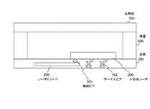
- FIG. 2 is a diagram showing an example of a cross-sectional view of the semiconductor laser driving device 10 according to the embodiment of the present technology.
- the substrate 100 in this example has a built-in laser driver 200, and a semiconductor laser 300 or the like is mounted on the surface thereof. At least a part of the semiconductor laser 300 and the laser driver 200 are arranged so as to be overlapped with each other, and the connection between the semiconductor laser 300 and the laser driver 200 is made via the connection via 101. By using this connection via 101, it is possible to shorten the wiring length.
- the substrate 100 includes a thermal via 102 for heat dissipation.
- Each component mounted on the substrate 100 is a heat source, and by using the thermal via 102, the heat generated in each component can be dissipated from the back surface of the substrate 100.
- the semiconductor laser 300, the photodiode 400, and the passive component 500 mounted on the surface of the substrate 100 are surrounded by the side wall 600.
- the material of the side wall 600 for example, a plastic material or a metal is assumed.
- the upper surface surrounded by the side wall 600 is covered with the diffuser plate 700.
- the diffuser plate 700 is an optical element for diffusing the laser beam from the semiconductor laser 300, and is also called a diffuser.
- FIG. 3 is a diagram showing an example of the circuit configuration of the laser driver 200 according to the embodiment of the present technology.
- the laser driver 200 includes a drive unit 210, a pulse data reception unit 220, an operation mode register 230, a temperature sensor 240, an abnormality detection unit 250, a switch 260, an AD converter 270, and a power supply control unit 280. , A constant current generation circuit 290 is provided.
- the drive unit 210 is a circuit for driving the semiconductor laser 300. As will be described later, the drive unit 210 includes a plurality of transistors connected to each of the plurality of laser diodes of the semiconductor laser 300 to drive the corresponding laser diodes. If the current is increased in order to light the semiconductor laser 300 brightly, the heat generation becomes larger. Therefore, this drive unit 210 becomes a main heat generating source in the laser driver 200.
- the pulse data receiving unit 220 receives pulse data supplied from the outside.
- This pulse data is a signal that is repeatedly turned on and off in order to cause the semiconductor laser 300 to emit light in the drive unit 210.
- the pulse data receiving unit 220 receives this pulse data as, for example, a differential signal of LVDS (Low Voltage Differential Signaling) standard, converts it into a non-differential signal, and supplies it to the driving unit 210.
- LVDS Low Voltage Differential Signaling
- the operation mode register 230 is a register for setting the operation mode of the drive unit 210.
- the operation mode register 230 holds the operation mode by receiving a communication clock, communication data, and a chip enable signal from the outside by an interface such as an SPI (Serial Peripheral Interface) standard.
- SPI Serial Peripheral Interface
- the temperature sensor 240 is a sensor that detects the temperature inside the laser driver 200. When the temperature detected by the temperature sensor 240 exceeds a predetermined temperature, the light emission of the semiconductor laser 300 is stopped by the control described later.
- the abnormality detection unit 250 is connected to the photodiode 400, monitors the light intensity of the semiconductor laser 300, maintains the output of the semiconductor laser 300 at a constant level, and detects the occurrence of an abnormality. For example, when it is detected that the diffuser plate 700 is broken, the light emission of the semiconductor laser 300 is stopped by the control described later.
- the switch 260 is a switch that selects signals from the temperature sensor 240 and the photodiode 400 and switches them to the AD converter 270.
- the AD converter (Analog-to-Digital Converter) 270 converts an analog signal from a temperature sensor 240 or the like supplied via a switch 260 into a digital signal.
- the converted digital signal is supplied to the power supply control unit 280.
- the power supply control unit 280 automatically controls the power supply for driving the semiconductor laser 300.
- a signal from the temperature sensor 240 and the photodiode 400 and an abnormality detection signal from the abnormality detection unit 250 are supplied to the power supply control unit 280, and power supply control is performed according to the situation.
- the constant current generation circuit 290 is a circuit that generates a current set by the power supply control unit 280.
- the constant current generation circuit 290 is configured by, for example, a DA converter (Digital-to-Analog Converter).
- the drive unit 210 operates by the current supplied from the constant current generation circuit 290.
- FIG. 4 is a diagram showing an example of the circuit configuration of the drive unit 210 according to the embodiment of the present technology.
- the semiconductor laser 300 is composed of a plurality of laser diodes 301, and the drive unit 210 includes transistors 211 corresponding to each of the laser diodes.
- the transistor 211 is assumed as the transistor 211.
- a voltage of 3 to 4 V is applied to the laser diode 301, and the laser diode 301 emits light by inputting a pulse signal from the constant current generation circuit 290 as the gate signal of the transistor 211 and performing on / off control. It is said.
- the drive unit 210 is composed of the transistor 211 corresponding to the laser diode 301, it can be distributed and arranged in the laser driver 200. However, it may be necessary to adjust the delay depending on the wiring distance.
- the drive unit 210 is the main heat source.
- the drive unit 210 will be focused on as a heat generating unit, and the relative arrangement relationship between the heat generating unit and the semiconductor laser 300 will be described.
- the heat generating part and the semiconductor laser 300 do not overlap (do not overlap) at a minimum. That is, if the heat generating portion and the semiconductor laser 300 are arranged so as to overlap each other, the heat from the heat generating portion directly interferes with the semiconductor laser 300, and the luminous efficiency of the semiconductor laser 300 may decrease. Therefore, when the laser driver 200 and the semiconductor laser 300 are arranged so as to overlap each other, it is desirable that the heat generating portion is arranged so as not to overlap the semiconductor laser 300.
- the distance between the drive unit 210 and the semiconductor laser 300 is more than 1 mm, the parasitic inductor due to wiring becomes large, and as a result, the waveform of the light may be accentuated and sharp rising and falling of light may not be obtained. There is. Therefore, from the viewpoint of the parasitic inductor, it is desirable that the distance between the heat generating portion and the semiconductor laser 300 is 1 mm.
- the distance between the heat generation part and the semiconductor laser 300 is preferably in the range of 0 to 1 mm.
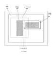
- FIG. 5 is a diagram showing a first example of the arrangement of the laser driver 200 and the semiconductor laser 300 in the embodiment of the present technology.
- the drive unit 210 that is, the heat generating unit 201 is arranged at one place of the laser driver 200. At that time, the distance between the heat generating portion 201 and the semiconductor laser 300 is arranged at a position of 0 to 1 mm. This makes it possible to achieve both heat generation and parasitic inductor conditions.
- FIG. 6 is a diagram showing a second example of the arrangement of the laser driver 200 and the semiconductor laser 300 in the embodiment of the present technology.
- the drive unit 210 that is, the heat generating units 202 and 203 are dispersedly arranged on both sides of the laser driver 200 at two locations. Since the drive unit 210 is composed of the transistors 211 corresponding to the laser diode 301 as described above, the drive unit 210 can be arranged in a dispersed manner. At that time, the distances between the heat generating portions 202 and 203 and the semiconductor laser 300 are all arranged at positions of 0 to 1 mm. This makes it possible to achieve both heat generation and parasitic inductor conditions.
- FIG. 7 is a diagram showing a third example of the arrangement of the laser driver 200 and the semiconductor laser 300 in the embodiment of the present technology.
- the driving unit 210 of the laser driver 200 that is, the heat generating unit 204 is arranged in an L shape on two sides around the semiconductor laser 300. Since the drive unit 210 is composed of the transistor 211 corresponding to the laser diode 301 as described above, the drive unit 210 can be arranged in any shape. At that time, the distance between the heat generating portion 204 and the semiconductor laser 300 is arranged at a position of 0 to 1 mm on each side. This makes it possible to achieve both heat generation and parasitic inductor conditions.
- FIG. 8 is a diagram showing a fourth example of arrangement of the laser driver 200 and the semiconductor laser 300 in the embodiment of the present technology.
- the driving unit 210 of the laser driver 200 that is, the heat generating unit 205 is arranged in a U shape on three sides around the semiconductor laser 300. Since the drive unit 210 is composed of the transistor 211 corresponding to the laser diode 301 as described above, the drive unit 210 can be arranged in any shape. At that time, the distance between the heat generating portion 205 and the semiconductor laser 300 is arranged at a position of 0 to 1 mm on each side. This makes it possible to achieve both heat generation and parasitic inductor conditions.
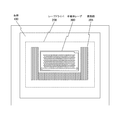
- FIG. 9 is a diagram showing a fifth example of arrangement of the laser driver 200 and the semiconductor laser 300 in the embodiment of the present technology.
- the driving unit 210 of the laser driver 200 that is, the heat generating unit 206 is arranged in a mouth shape on four sides around the semiconductor laser 300. Since the drive unit 210 is composed of the transistor 211 corresponding to the laser diode 301 as described above, the drive unit 210 can be arranged in any shape. At that time, the distance between the heat generating portion 206 and the semiconductor laser 300 is arranged at a position of 0 to 1 mm on each side. This makes it possible to achieve both heat generation and parasitic inductor conditions.
- the drive unit 210 of the laser driver 200 and the semiconductor laser 300 so as not to overlap with each other, the influence of heat generated by the drive unit 210 on the semiconductor laser 300 is suppressed. can do. Further, by arranging the distance between the driving unit 210 of the laser driver 200 and the semiconductor laser 300 at 0 to 1 mm, it is possible to suppress the influence of the parasitic inductor on the waveform of light.
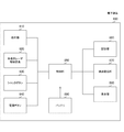
- FIG. 10 is a diagram showing a system configuration example of the electronic device 800, which is an application example of the embodiment of the present technology.
- the electronic device 800 is a mobile terminal equipped with the semiconductor laser drive device 10 according to the above-described embodiment.
- the electronic device 800 includes an imaging unit 810, a semiconductor laser driving device 820, a shutter button 830, a power button 840, a control unit 850, a storage unit 860, a wireless communication unit 870, a display unit 880, and a battery. It is equipped with 890.
- the imaging unit 810 is an image sensor that captures an image of the subject.
- the semiconductor laser driving device 820 is the semiconductor laser driving device 10 according to the above-described embodiment.
- the shutter button 830 is a button for instructing the imaging timing in the imaging unit 810 from the outside of the electronic device 800.
- the power button 840 is a button for instructing the on / off of the power of the electronic device 800 from the outside of the electronic device 800.
- the control unit 850 is a processing unit that controls the entire electronic device 800.
- the storage unit 860 is a memory that stores data and programs necessary for the operation of the electronic device 800.
- the wireless communication unit 870 performs wireless communication with the outside of the electronic device 800.
- the display unit 880 is a display for displaying an image or the like.
- the battery 890 is a power supply source that supplies power to each part of the electronic device 800.
- a specific phase (for example, rise timing) of the light emission control signal that controls the image pickup unit 810 and the semiconductor laser drive device 820 is set to 0 degree, and the received light amount from 0 degree to 180 degree is detected as Q1 and is detected from 180 degree to 360 degree.
- the amount of light received up to is detected as Q2.
- the imaging unit 810 detects the light receiving amount from 90 degrees to 270 degrees as Q3, and detects the light receiving amount from 270 degrees to 90 degrees as Q4.
- the control unit 850 calculates the distance d from the object from the received light amounts Q1 to Q4 by the following equation, and displays the distance d on the display unit 880.
- the unit of the distance d is, for example, meters (m).
- c is the speed of light, the unit of which is, for example, meters per second (m / s).
- arctan is the inverse of the tangent function.
- the value of "(Q3-Q4) / (Q1-Q2)" indicates the phase difference between the irradiation light and the reflected light.
- ⁇ indicates the pi.
- f is the frequency of the irradiation light, and the unit thereof is, for example, megahertz (MHz).
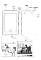
- FIG. 11 is a diagram showing an example of an external configuration of an electronic device 800, which is an application example of the embodiment of the present technology.
- This electronic device 800 is housed in a housing 801 and is provided with a power button 840 on the side surface and a display unit 880 and a shutter button 830 on the front surface. Further, an optical region of the imaging unit 810 and the semiconductor laser driving device 820 is provided on the back surface.
- the normal captured image 881 can be displayed on the display unit 880, but also the depth image 882 according to the distance measurement result using ToF can be displayed.
- a mobile terminal such as a smartphone is illustrated as the electronic device 800, but the electronic device 800 is not limited to this, and may be, for example, a digital camera, a game machine, a wearable device, or the like. good.
- the present technology can have the following configurations.
- the semiconductor laser includes a plurality of laser diodes and has a plurality of laser diodes.
- the semiconductor laser driving device according to any one of (1) to (4) above, wherein the heat generating portion is a plurality of transistors for driving the corresponding laser diode among the plurality of laser diodes.
- the semiconductor laser driving device according to any one of (1) to (5) above, wherein the heat generating portion is arranged at a predetermined location of the laser driver.
- the semiconductor laser driving device according to any one of (1) to (5) above, wherein the heat generating portions are dispersedly arranged at a plurality of predetermined locations of the laser driver.
- the semiconductor laser driving device according to any one of (1) to (7), wherein the heat generating portion is arranged in a predetermined shape around the semiconductor laser.
Landscapes
- Physics & Mathematics (AREA)
- General Physics & Mathematics (AREA)
- Engineering & Computer Science (AREA)
- Electromagnetism (AREA)
- Condensed Matter Physics & Semiconductors (AREA)
- Optics & Photonics (AREA)
- Computer Networks & Wireless Communication (AREA)
- Radar, Positioning & Navigation (AREA)
- Remote Sensing (AREA)
- Semiconductor Lasers (AREA)
- Optical Radar Systems And Details Thereof (AREA)
Abstract
半導体レーザ駆動装置において、半導体レーザを駆動するレーザドライバの発熱分布を考慮して部品配置を行う。 半導体レーザ駆動装置は、半導体レーザとレーザドライバとを備える。レーザドライバは、半導体レーザに対して少なくとも一部が重ねて配置される。一方で、レーザドライバの発熱部と半導体レーザとは、重なることなく配置される。発熱部は、例えば、半導体レーザを駆動する回路である。発熱部は、レーザドライバの1個所に配置されてもよく、また、複数個所に分散配置されてもよい。
Description
本技術は、半導体レーザ駆動装置に関する。詳しくは、レーザドライバ内蔵基板と半導体レーザとを備える半導体レーザ駆動装置に関する。
従来、測距機能を持つ電子装置において、ToF(Time of Flight)と呼ばれる測距方式がよく用いられている。このToFは、発光部がサイン波や矩形波の照射光を物体に照射し、その物体からの反射光を受光部が受光して、測距演算部が照射光と反射光との位相差から距離を測定する方式である。そのような測距機能を実現するため、発光素子と、その発光素子を駆動する電子半導体チップとをケース内に収容して一体化した光モジュールが知られている。例えば、基板の電極パターン上に整列して実装されたレーザーダイオードアレイと、レーザーダイオードアレイに電気的に接続されたドライバICとを備える光モジュールが提案されている(例えば、特許文献1参照。)。
上述の従来技術では、電子素子を含む部品全体を覆うカバーを熱伝導材料で構成することにより、発熱を促す構造を採用している。しかしながら、この従来技術では、熱の分布に偏りがあった場合であっても、全体を均等に扱うため、発熱の効率が低下するという問題がある。
本技術はこのような状況に鑑みて生み出されたものであり、半導体レーザを駆動するレーザドライバの発熱分布を考慮して部品配置を行うことを目的とする。
本技術は、上述の問題点を解消するためになされたものであり、その第1の側面は、半導体レーザと、上記半導体レーザに対して少なくとも一部が重ねて配置されるレーザドライバとを具備し、上記レーザドライバの発熱部と上記半導体レーザとが重なることなく配置された半導体レーザ駆動装置である。これにより、レーザドライバの発熱部から発生した熱が半導体レーザに与える影響を抑制するという作用をもたらす。
また、この第1の側面において、上記レーザドライバの発熱部と上記半導体レーザとの距離が1ミリメートル以下であることが望ましい。これにより、寄生インダクタが光の波形に与える影響を抑制するという作用をもたらす。
また、この第1の側面において、上記レーザドライバは、上記半導体レーザを搭載する基板に内蔵されてもよい。これにより、半導体レーザ駆動装置を低背化するという作用をもたらす。
また、この第1の側面において、上記発熱部は、上記半導体レーザを駆動する回路であると想定してもよい。また、この第1の側面において、上記半導体レーザは、複数のレーザダイオードを備え、上記発熱部は、上記複数のレーザダイオードのうち対応するレーザダイオードを駆動する複数のトランジスタであってもよい。
また、この第1の側面において、上記発熱部は、上記レーザドライバの所定の1個所に配置されてもよく、また、上記レーザドライバの所定の複数個所に分散配置されてもよい。また、上記発熱部は、上記半導体レーザの周囲において所定の形状に配置されてもよい。
以下、本技術を実施するための形態(以下、実施の形態と称する)について説明する。説明は以下の順序により行う。
1.実施の形態
2.適用例
1.実施の形態
2.適用例
<1.実施の形態>
[半導体レーザ駆動装置]
図1は、本技術の実施の形態における半導体レーザ駆動装置10の上面図の一例を示す図である。
[半導体レーザ駆動装置]
図1は、本技術の実施の形態における半導体レーザ駆動装置10の上面図の一例を示す図である。
この半導体レーザ駆動装置10は、ToFによる距離の測定を想定したものである。ToFは、ストラクチャードライトほどではないものの奥行き精度が高く、また、暗い環境下でも問題なく動作可能という特徴を有する。他にも、装置構成の単純さや、コストなどにおいて、ストラクチャードライトやステレオカメラなどの他の方式と比べてメリットが多いと考えられる。
この半導体レーザ駆動装置10では、レーザドライバ200を内蔵する基板100の表面に、半導体レーザ300、フォトダイオード400および受動部品500がワイヤボンディングにより電気接続されて実装される。基板100としては、プリント配線板が想定される。
半導体レーザ300は、化合物半導体のPN接合に電流を流すことにより、レーザ光を放射する半導体デバイスである。この半導体レーザ300は、複数のレーザダイオードにより構成される。ここで、利用される化合物半導体としては、例えば、アルミニウムガリウム砒素(AlGaAs)、インジウムガリウム砒素リン(InGaAsP)、アルミニウムガリウムインジウムリン(AlGaInP)、ガリウムナイトライド(GaN)などが想定される。
レーザドライバ200は、半導体レーザ300を駆動するためのドライバ集積回路(IC:Integrated Circuit)である。この例において、レーザドライバ200は、フェイスアップ状態で基板100に内蔵される。
フォトダイオード400は、光を検出するためのダイオードである。このフォトダイオード400は、半導体レーザ300の光強度を監視して、半導体レーザ300の出力を一定に維持するための自動電源制御(APC:Automatic Power Control)に用いられる。
受動部品500は、コンデンサおよび抵抗などの能動素子以外の回路部品である。この受動部品500には、半導体レーザ300を駆動するためのデカップリングコンデンサが含まれる。
図2は、本技術の実施の形態における半導体レーザ駆動装置10の断面図の一例を示す図である。
上述のように、この例における基板100はレーザドライバ200を内蔵し、その表面には半導体レーザ300などが実装される。半導体レーザ300とレーザドライバ200は、少なくとも一部が重ねて配置され、両者の間の接続は、接続ビア101を介して行われる。この接続ビア101を用いることにより、配線長を短くすることが可能となる。
また、基板100は、放熱のためのサーマルビア102を備える。基板100に実装された各部品は発熱源であり、サーマルビア102を用いることにより、各部品において発生した熱を基板100の裏面から放熱することが可能となる。
基板100の表面に実装された半導体レーザ300、フォトダイオード400および受動部品500は、側壁600によって囲まれる。この側壁600の材料としては、例えば、プラスティック材料、または、金属が想定される。
側壁600によって囲まれた上面は、拡散板700によって覆われる。この拡散板700は、半導体レーザ300からのレーザ光を拡散させるための光学素子であり、ディフューザとも呼ばれる。
[レーザドライバ]
図3は、本技術の実施の形態におけるレーザドライバ200の回路構成の一例を示す図である。
図3は、本技術の実施の形態におけるレーザドライバ200の回路構成の一例を示す図である。
このレーザドライバ200は、駆動部210と、パルスデータ受信部220と、動作モードレジスタ230と、温度センサ240と、異常検知部250と、スイッチ260と、AD変換器270と、電源制御部280と、定電流発生回路290とを備える。
駆動部210は、半導体レーザ300を駆動するための回路である。後述するように、この駆動部210は、半導体レーザ300の複数のレーザダイオードの各々に接続し、対応するレーザダイオードを駆動するトランジスタを複数備える。半導体レーザ300を明るく点灯させるために電流を増やせば、より発熱が大きくなる。そのため、この駆動部210がレーザドライバ200における主要な発熱源となる。
パルスデータ受信部220は、外部から供給されるパルスデータを受信するものである。このパルスデータは、駆動部210において半導体レーザ300を発光させるためにオンおよびオフを繰り返す信号である。パルスデータ受信部220は、このパルスデータを、例えばLVDS(Low Voltage Differential Signaling)規格の差動信号として受信し、非差動信号に変換して駆動部210に供給する。
動作モードレジスタ230は、駆動部210の動作モードを設定するためのレジスタである。この動作モードレジスタ230は、例えばSPI(Serial Peripheral Interface)規格等のインターフェースにより、外部から通信用クロック、通信用データおよびチップイネーブル信号を受けて、動作モードを保持する。
温度センサ240は、レーザドライバ200内部の温度を検知するセンサである。この温度センサ240により検知された温度が所定の温度を超えると、後述する制御により半導体レーザ300の発光が停止される。
異常検知部250は、フォトダイオード400に接続し、半導体レーザ300の光強度を監視して半導体レーザ300の出力を一定に維持するとともに、異常の発生を検知するものである。例えば、拡散板700が割れたことが検知されると、後述する制御により半導体レーザ300の発光が停止される。
スイッチ260は、温度センサ240やフォトダイオード400からの信号を選択してAD変換器270に切り替えるスイッチである。
AD変換器(Analog-to-Digital Converter)270は、スイッチ260を介して供給された温度センサ240等からのアナログ信号を、デジタル信号に変換するものである。変換されたデジタル信号は、電源制御部280に供給される。
電源制御部280は、半導体レーザ300を駆動するための電源の自動電源制御を行うものである。この電源制御部280には、温度センサ240やフォトダイオード400からの信号、および、異常検知部250からの異常検知信号が供給され、状況に応じた電源制御が行われる。
定電流発生回路290は、電源制御部280により設定された電流を発生する回路である。この定電流発生回路290は、例えばDA変換器(Digital-to-Analog Converter)により構成される。駆動部210は、この定電流発生回路290から供給された電流により動作する。
図4は、本技術の実施の形態における駆動部210の回路構成の一例を示す図である。
上述のように、半導体レーザ300は複数のレーザダイオード301により構成され、駆動部210はレーザダイオードの各々に対応するトランジスタ211を備える。この例では、トランジスタ211としてnMOSトランジスタを想定する。
レーザダイオード301には3乃至4Vの電圧が印加されており、トランジスタ211のゲート信号として定電流発生回路290からのパルス信号を入力して、オンオフ制御を行うことにより、レーザダイオード301の発光が行われる。
このように、駆動部210はレーザダイオード301に対応するトランジスタ211から構成されるため、レーザドライバ200において分散して配置することが可能である。ただし、配線距離によっては遅延調整を行う必要が生じ得る。
[回路配置]
上述のように、レーザドライバ200において駆動部210が主要な発熱源となる。以下では、この駆動部210を発熱部として着目し、発熱部と半導体レーザ300との相対的な配置関係について説明する。
上述のように、レーザドライバ200において駆動部210が主要な発熱源となる。以下では、この駆動部210を発熱部として着目し、発熱部と半導体レーザ300との相対的な配置関係について説明する。
発熱部に対する熱対策として、最低限、発熱部と半導体レーザ300とが重ならない(オーバラップしない)ことが望ましい。すなわち、発熱部と半導体レーザ300とが重ねて配置されると、発熱部からの熱が半導体レーザ300に直接干渉することになり、半導体レーザ300の発光効率が低下するおそれがある。そのため、レーザドライバ200と半導体レーザ300とが重ねて配置される際、発熱部が半導体レーザ300に重ならないように配置することが望ましい。
一方、駆動部210と半導体レーザ300との距離が1ミリメートルよりも離れると、配線による寄生インダクタが大きくなり、その影響で光の波形が訛り、シャープな光の立上りおよび立下りが得られなくなるおそれがある。そのため、寄生インダクタの観点からは、発熱部と半導体レーザ300との距離を1ミリメートルにすることが望ましい。
したがって、発熱および寄生インダクタの両者を考慮すると、発熱部と半導体レーザ300との距離は、0乃至1ミリメートルの範囲内であることが望ましい。
図5は、本技術の実施の形態におけるレーザドライバ200と半導体レーザ300の配置の第1の例を示す図である。
この第1の例では、レーザドライバ200の1個所に駆動部210、すなわち発熱部201を配置している。その際、発熱部201と半導体レーザ300との距離は、0乃至1ミリメートルの位置に配置される。これにより、発熱および寄生インダクタの条件を両立させることができる。
図6は、本技術の実施の形態におけるレーザドライバ200と半導体レーザ300の配置の第2の例を示す図である。
この第2の例では、レーザドライバ200の2個所に駆動部210、すなわち発熱部202および203を両脇に分散して配置している。駆動部210は、上述のようにレーザダイオード301に対応するトランジスタ211から構成されるため、分散して配置することが可能である。その際、発熱部202および203と半導体レーザ300との距離は、何れも0乃至1ミリメートルの位置に配置される。これにより、発熱および寄生インダクタの条件を両立させることができる。
図7は、本技術の実施の形態におけるレーザドライバ200と半導体レーザ300の配置の第3の例を示す図である。
この第3の例では、レーザドライバ200の駆動部210、すなわち発熱部204を、半導体レーザ300の周囲2辺において、Lの字型に配置している。駆動部210は、上述のようにレーザダイオード301に対応するトランジスタ211から構成されるため、任意の形状により配置することが可能である。その際、発熱部204と半導体レーザ300との距離は、何れの辺も0乃至1ミリメートルの位置に配置される。これにより、発熱および寄生インダクタの条件を両立させることができる。
図8は、本技術の実施の形態におけるレーザドライバ200と半導体レーザ300の配置の第4の例を示す図である。
この第4の例では、レーザドライバ200の駆動部210、すなわち発熱部205を、半導体レーザ300の周囲3辺において、コの字型に配置している。駆動部210は、上述のようにレーザダイオード301に対応するトランジスタ211から構成されるため、任意の形状により配置することが可能である。その際、発熱部205と半導体レーザ300との距離は、何れの辺も0乃至1ミリメートルの位置に配置される。これにより、発熱および寄生インダクタの条件を両立させることができる。
図9は、本技術の実施の形態におけるレーザドライバ200と半導体レーザ300の配置の第5の例を示す図である。
この第5の例では、レーザドライバ200の駆動部210、すなわち発熱部206を、半導体レーザ300の周囲4辺において、口の字型に配置している。駆動部210は、上述のようにレーザダイオード301に対応するトランジスタ211から構成されるため、任意の形状により配置することが可能である。その際、発熱部206と半導体レーザ300との距離は、何れの辺も0乃至1ミリメートルの位置に配置される。これにより、発熱および寄生インダクタの条件を両立させることができる。
このように、本技術の実施の形態によれば、レーザドライバ200の駆動部210と半導体レーザ300とが重ならないように配置することにより、駆動部210における発熱が半導体レーザ300に与える影響を抑制することができる。また、レーザドライバ200の駆動部210と半導体レーザ300との距離を0乃至1ミリメートルに配置することにより、寄生インダクタが光の波形に与える影響を抑制することができる。
<2.適用例>
[電子機器]
図10は、本技術の実施の形態の適用例である電子機器800のシステム構成例を示す図である。
[電子機器]
図10は、本技術の実施の形態の適用例である電子機器800のシステム構成例を示す図である。
この電子機器800は、上述の実施の形態による半導体レーザ駆動装置10を搭載した携帯端末である。この電子機器800は、撮像部810と、半導体レーザ駆動装置820と、シャッタボタン830と、電源ボタン840と、制御部850と、記憶部860と、無線通信部870と、表示部880と、バッテリ890とを備える。
撮像部810は、被写体を撮像するイメージセンサである。半導体レーザ駆動装置820は、上述の実施の形態による半導体レーザ駆動装置10である。
シャッタボタン830は、撮像部810における撮像タイミングを電子機器800の外部から指示するためのボタンである。電源ボタン840は、電子機器800の電源のオンオフを電子機器800の外部から指示するためのボタンである。
制御部850は、電子機器800の全体の制御を司る処理部である。記憶部860は、電子機器800の動作に必要なデータやプログラムを記憶するメモリである。無線通信部870は、電子機器800の外部との無線通信を行うものである。表示部880は、画像等を表示するディスプレイである。バッテリ890は、電子機器800の各部に電源を供給する電源供給源である。
撮像部810、半導体レーザ駆動装置820を制御する発光制御信号の特定の位相(例えば、立上りタイミング)を0度として、0度から180度までの受光量をQ1として検出し、180度から360度までの受光量をQ2として検出する。また、撮像部810は、90度から270度までの受光量をQ3として検出し、270度から90度までの受光量をQ4として検出する。制御部850は、これらの受光量Q1乃至Q4から、次式により物体との距離dを演算し、表示部880に表示する。
d=(c/4πf)×arctan{(Q3-Q4)/(Q1-Q2)}
上式において距離dの単位は、例えば、メートル(m)である。cは光速であり、その単位は、例えば、メートル毎秒(m/s)である。arctanは、正接関数の逆関数である。「(Q3-Q4)/(Q1-Q2)」の値は、照射光と反射光との位相差を示す。πは、円周率を示す。また、fは照射光の周波数であり、その単位は、例えば、メガヘルツ(MHz)である。
図11は、本技術の実施の形態の適用例である電子機器800の外観構成例を示す図である。
この電子機器800は、筐体801に収められ、側面に電源ボタン840を備え、表面に表示部880およびシャッタボタン830を備える。また、裏面には撮像部810および半導体レーザ駆動装置820の光学領域が設けられる。
これにより、表示部880には、通常の撮像画像881を表示するだけでなく、ToFを利用した測距結果に応じた奥行画像882を表示することができる。
なお、この適用例では、電子機器800として、スマートフォンのような携帯端末について例示したが、電子機器800はこれに限定されるものではなく、例えばデジタルカメラやゲーム機やウェアラブル機器などであってもよい。
なお、上述の実施の形態は本技術を具現化するための一例を示したものであり、実施の形態における事項と、特許請求の範囲における発明特定事項とはそれぞれ対応関係を有する。同様に、特許請求の範囲における発明特定事項と、これと同一名称を付した本技術の実施の形態における事項とはそれぞれ対応関係を有する。ただし、本技術は実施の形態に限定されるものではなく、その要旨を逸脱しない範囲において実施の形態に種々の変形を施すことにより具現化することができる。
なお、本明細書に記載された効果はあくまで例示であって、限定されるものではなく、また、他の効果があってもよい。
なお、本技術は以下のような構成もとることができる。
(1)半導体レーザと、
前記半導体レーザに対して少なくとも一部が重ねて配置されるレーザドライバと
を具備し、
前記レーザドライバの発熱部と前記半導体レーザとが重なることなく配置された半導体レーザ駆動装置。
(2)前記レーザドライバの発熱部と前記半導体レーザとの距離が1ミリメートル以下である前記(1)に記載の半導体レーザ駆動装置。
(3)前記レーザドライバは、前記半導体レーザを搭載する基板に内蔵される
前記(1)または(2)に記載の半導体レーザ駆動装置。
(4)前記発熱部は、前記半導体レーザを駆動する回路である
前記(1)から(3)のいずれかに記載の半導体レーザ駆動装置。
(5)前記半導体レーザは、複数のレーザダイオードを備え、
前記発熱部は、前記複数のレーザダイオードのうち対応するレーザダイオードを駆動する複数のトランジスタである
前記(1)から(4)のいずれかに記載の半導体レーザ駆動装置。
(6)前記発熱部は、前記レーザドライバの所定の1個所に配置される
前記(1)から(5)のいずれかに記載の半導体レーザ駆動装置。
(7)前記発熱部は、前記レーザドライバの所定の複数個所に分散配置される
前記(1)から(5)のいずれかに記載の半導体レーザ駆動装置。
(8)前記発熱部は、前記半導体レーザの周囲において所定の形状に配置される
前記(1)から(7)のいずれかに記載の半導体レーザ駆動装置。
(1)半導体レーザと、
前記半導体レーザに対して少なくとも一部が重ねて配置されるレーザドライバと
を具備し、
前記レーザドライバの発熱部と前記半導体レーザとが重なることなく配置された半導体レーザ駆動装置。
(2)前記レーザドライバの発熱部と前記半導体レーザとの距離が1ミリメートル以下である前記(1)に記載の半導体レーザ駆動装置。
(3)前記レーザドライバは、前記半導体レーザを搭載する基板に内蔵される
前記(1)または(2)に記載の半導体レーザ駆動装置。
(4)前記発熱部は、前記半導体レーザを駆動する回路である
前記(1)から(3)のいずれかに記載の半導体レーザ駆動装置。
(5)前記半導体レーザは、複数のレーザダイオードを備え、
前記発熱部は、前記複数のレーザダイオードのうち対応するレーザダイオードを駆動する複数のトランジスタである
前記(1)から(4)のいずれかに記載の半導体レーザ駆動装置。
(6)前記発熱部は、前記レーザドライバの所定の1個所に配置される
前記(1)から(5)のいずれかに記載の半導体レーザ駆動装置。
(7)前記発熱部は、前記レーザドライバの所定の複数個所に分散配置される
前記(1)から(5)のいずれかに記載の半導体レーザ駆動装置。
(8)前記発熱部は、前記半導体レーザの周囲において所定の形状に配置される
前記(1)から(7)のいずれかに記載の半導体レーザ駆動装置。
10 半導体レーザ駆動装置
100 基板
101 接続ビア
102 サーマルビア
200 レーザドライバ
201~206 発熱部
210 駆動部
211 トランジスタ(nMOSトランジスタ)
220 パルスデータ受信部
230 動作モードレジスタ
240 温度センサ
250 異常検知部
260 スイッチ
270 AD変換器
280 電源制御部
290 定電流発生回路
300 半導体レーザ
301 レーザダイオード
400 フォトダイオード
500 受動部品
600 側壁
700 拡散板
800 電子機器
801 筐体
810 撮像部
820 半導体レーザ駆動装置
830 シャッタボタン
840 電源ボタン
850 制御部
860 記憶部
870 無線通信部
880 表示部
881 撮像画像
882 奥行画像
890 バッテリ
100 基板
101 接続ビア
102 サーマルビア
200 レーザドライバ
201~206 発熱部
210 駆動部
211 トランジスタ(nMOSトランジスタ)
220 パルスデータ受信部
230 動作モードレジスタ
240 温度センサ
250 異常検知部
260 スイッチ
270 AD変換器
280 電源制御部
290 定電流発生回路
300 半導体レーザ
301 レーザダイオード
400 フォトダイオード
500 受動部品
600 側壁
700 拡散板
800 電子機器
801 筐体
810 撮像部
820 半導体レーザ駆動装置
830 シャッタボタン
840 電源ボタン
850 制御部
860 記憶部
870 無線通信部
880 表示部
881 撮像画像
882 奥行画像
890 バッテリ
Claims (8)
- 半導体レーザと、
前記半導体レーザに対して少なくとも一部が重ねて配置されるレーザドライバと
を具備し、
前記レーザドライバの発熱部と前記半導体レーザとが重なることなく配置された半導体レーザ駆動装置。 - 前記レーザドライバの発熱部と前記半導体レーザとの距離が1ミリメートル以下である請求項1記載の半導体レーザ駆動装置。
- 前記レーザドライバは、前記半導体レーザを搭載する基板に内蔵される
請求項1記載の半導体レーザ駆動装置。 - 前記発熱部は、前記半導体レーザを駆動する回路である
請求項1記載の半導体レーザ駆動装置。 - 前記半導体レーザは、複数のレーザダイオードを備え、
前記発熱部は、前記複数のレーザダイオードのうち対応するレーザダイオードを駆動する複数のトランジスタである
請求項1記載の半導体レーザ駆動装置。 - 前記発熱部は、前記レーザドライバの所定の1個所に配置される
請求項1記載の半導体レーザ駆動装置。 - 前記発熱部は、前記レーザドライバの所定の複数個所に分散配置される
請求項1記載の半導体レーザ駆動装置。 - 前記発熱部は、前記半導体レーザの周囲において所定の形状に配置される
請求項1記載の半導体レーザ駆動装置。
Priority Applications (1)
| Application Number | Priority Date | Filing Date | Title |
|---|---|---|---|
| JP2022505798A JP7565333B2 (ja) | 2020-03-11 | 2021-01-14 | 半導体レーザ駆動装置 |
Applications Claiming Priority (2)
| Application Number | Priority Date | Filing Date | Title |
|---|---|---|---|
| JP2020-041528 | 2020-03-11 | ||
| JP2020041528 | 2020-03-11 |
Publications (1)
| Publication Number | Publication Date |
|---|---|
| WO2021181862A1 true WO2021181862A1 (ja) | 2021-09-16 |
Family
ID=77672212
Family Applications (1)
| Application Number | Title | Priority Date | Filing Date |
|---|---|---|---|
| PCT/JP2021/000994 Ceased WO2021181862A1 (ja) | 2020-03-11 | 2021-01-14 | 半導体レーザ駆動装置 |
Country Status (2)
| Country | Link |
|---|---|
| JP (1) | JP7565333B2 (ja) |
| WO (1) | WO2021181862A1 (ja) |
Citations (4)
| Publication number | Priority date | Publication date | Assignee | Title |
|---|---|---|---|---|
| JPH05145195A (ja) * | 1991-11-19 | 1993-06-11 | Nippon Telegr & Teleph Corp <Ntt> | 面発光半導体レーザ |
| JPH11121735A (ja) * | 1997-08-27 | 1999-04-30 | Xerox Corp | 集積化半導体レーザー及び構成部品構造 |
| JP2002232062A (ja) * | 2001-02-02 | 2002-08-16 | Ricoh Co Ltd | 光電子集積素子 |
| WO2019202874A1 (ja) * | 2018-04-19 | 2019-10-24 | ソニーセミコンダクタソリューションズ株式会社 | 半導体レーザ駆動装置およびその製造方法 |
-
2021
- 2021-01-14 WO PCT/JP2021/000994 patent/WO2021181862A1/ja not_active Ceased
- 2021-01-14 JP JP2022505798A patent/JP7565333B2/ja active Active
Patent Citations (4)
| Publication number | Priority date | Publication date | Assignee | Title |
|---|---|---|---|---|
| JPH05145195A (ja) * | 1991-11-19 | 1993-06-11 | Nippon Telegr & Teleph Corp <Ntt> | 面発光半導体レーザ |
| JPH11121735A (ja) * | 1997-08-27 | 1999-04-30 | Xerox Corp | 集積化半導体レーザー及び構成部品構造 |
| JP2002232062A (ja) * | 2001-02-02 | 2002-08-16 | Ricoh Co Ltd | 光電子集積素子 |
| WO2019202874A1 (ja) * | 2018-04-19 | 2019-10-24 | ソニーセミコンダクタソリューションズ株式会社 | 半導体レーザ駆動装置およびその製造方法 |
Also Published As
| Publication number | Publication date |
|---|---|
| JPWO2021181862A1 (ja) | 2021-09-16 |
| JP7565333B2 (ja) | 2024-10-10 |
Similar Documents
| Publication | Publication Date | Title |
|---|---|---|
| KR102674040B1 (ko) | 발광 장치, 광학 장치 및 정보 처리 장치 | |
| US20180136454A1 (en) | Light source apparatus | |
| JP5060017B2 (ja) | プロジェクタ | |
| US12155169B2 (en) | Light emitting module including enhanced eye-safety feature | |
| WO2020161932A1 (ja) | 発光装置、光学装置および情報処理装置 | |
| US20170123064A1 (en) | Proximity sensor, electronic apparatus and method for manufacturing proximity sensor | |
| EP3417682B1 (en) | Laser diode chip on printed circuit board | |
| CN111665511B (zh) | 测距装置 | |
| US8902947B2 (en) | Optical module | |
| WO2019172240A1 (ja) | 光源モジュール | |
| WO2021256053A1 (ja) | 発光装置および距離測定装置 | |
| WO2021181862A1 (ja) | 半導体レーザ駆動装置 | |
| US7245648B2 (en) | Optoelectronic arrangement | |
| KR102211153B1 (ko) | 카메라 모듈형 센서 장치 및 카메라 모듈 | |
| JP2010093752A (ja) | 固体撮像素子及び信号処理システム | |
| WO2022124059A1 (ja) | 測距装置 | |
| EP3487274A1 (en) | Electronic device comprising a structral piece with a cage positionned over an electronic component | |
| US11711621B2 (en) | Electronic device and method for an electronic device | |
| CN216526280U (zh) | 一种激光驱动电路 | |
| CN112420800A (zh) | 显示模组以及电子设备 | |
| WO2020183935A1 (ja) | 故障検出装置、発光駆動装置および発光装置 | |
| US20250347779A1 (en) | Lidar device | |
| CN113196090A (zh) | 发光驱动电路和发光装置 | |
| JP2022022603A (ja) | 画像投影装置および車両用灯具 | |
| JP2004053306A (ja) | 光学式測距装置 |
Legal Events
| Date | Code | Title | Description |
|---|---|---|---|
| 121 | Ep: the epo has been informed by wipo that ep was designated in this application |
Ref document number: 21768630 Country of ref document: EP Kind code of ref document: A1 |
|
| ENP | Entry into the national phase |
Ref document number: 2022505798 Country of ref document: JP Kind code of ref document: A |
|
| NENP | Non-entry into the national phase |
Ref country code: DE |
|
| 122 | Ep: pct application non-entry in european phase |
Ref document number: 21768630 Country of ref document: EP Kind code of ref document: A1 |