WO2021167060A1 - Solid-state imaging device - Google Patents
Solid-state imaging device Download PDFInfo
- Publication number
- WO2021167060A1 WO2021167060A1 PCT/JP2021/006326 JP2021006326W WO2021167060A1 WO 2021167060 A1 WO2021167060 A1 WO 2021167060A1 JP 2021006326 W JP2021006326 W JP 2021006326W WO 2021167060 A1 WO2021167060 A1 WO 2021167060A1
- Authority
- WO
- WIPO (PCT)
- Prior art keywords
- layer
- solid
- semiconductor layer
- separation groove
- state image
- Prior art date
Links
- 238000003384 imaging method Methods 0.000 title claims abstract description 12
- 239000004065 semiconductor Substances 0.000 claims abstract description 65
- 238000006243 chemical reaction Methods 0.000 claims abstract description 11
- 230000002093 peripheral effect Effects 0.000 claims description 22
- 238000003860 storage Methods 0.000 claims description 19
- 238000000926 separation method Methods 0.000 claims description 16
- 229910018072 Al 2 O 3 Inorganic materials 0.000 claims description 4
- 230000000149 penetrating effect Effects 0.000 claims description 4
- 238000009751 slip forming Methods 0.000 claims 1
- 238000009825 accumulation Methods 0.000 abstract description 8
- 238000002955 isolation Methods 0.000 abstract description 4
- 238000000034 method Methods 0.000 description 17
- 238000010586 diagram Methods 0.000 description 14
- 229910044991 metal oxide Inorganic materials 0.000 description 14
- 150000004706 metal oxides Chemical class 0.000 description 14
- 238000004519 manufacturing process Methods 0.000 description 12
- RYGMFSIKBFXOCR-UHFFFAOYSA-N Copper Chemical compound [Cu] RYGMFSIKBFXOCR-UHFFFAOYSA-N 0.000 description 10
- 229910052802 copper Inorganic materials 0.000 description 10
- 239000010949 copper Substances 0.000 description 10
- 239000000758 substrate Substances 0.000 description 10
- 230000035945 sensitivity Effects 0.000 description 8
- 229910052710 silicon Inorganic materials 0.000 description 8
- 239000010703 silicon Substances 0.000 description 8
- XUIMIQQOPSSXEZ-UHFFFAOYSA-N Silicon Chemical compound [Si] XUIMIQQOPSSXEZ-UHFFFAOYSA-N 0.000 description 7
- 239000012535 impurity Substances 0.000 description 4
- 238000005229 chemical vapour deposition Methods 0.000 description 3
- 230000000052 comparative effect Effects 0.000 description 2
- 238000005530 etching Methods 0.000 description 2
- 239000000463 material Substances 0.000 description 2
- 239000011159 matrix material Substances 0.000 description 2
- 238000010521 absorption reaction Methods 0.000 description 1
- 229910052782 aluminium Inorganic materials 0.000 description 1
- XAGFODPZIPBFFR-UHFFFAOYSA-N aluminium Chemical compound [Al] XAGFODPZIPBFFR-UHFFFAOYSA-N 0.000 description 1
- 238000005452 bending Methods 0.000 description 1
- 230000015572 biosynthetic process Effects 0.000 description 1
- 238000005520 cutting process Methods 0.000 description 1
- 230000006866 deterioration Effects 0.000 description 1
- 238000005516 engineering process Methods 0.000 description 1
- CJNBYAVZURUTKZ-UHFFFAOYSA-N hafnium(iv) oxide Chemical compound O=[Hf]=O CJNBYAVZURUTKZ-UHFFFAOYSA-N 0.000 description 1
- 238000002347 injection Methods 0.000 description 1
- 239000007924 injection Substances 0.000 description 1
- 238000009413 insulation Methods 0.000 description 1
- 238000001459 lithography Methods 0.000 description 1
- 238000012986 modification Methods 0.000 description 1
- 230000004048 modification Effects 0.000 description 1
- TWNQGVIAIRXVLR-UHFFFAOYSA-N oxo(oxoalumanyloxy)alumane Chemical compound O=[Al]O[Al]=O TWNQGVIAIRXVLR-UHFFFAOYSA-N 0.000 description 1
- 238000007747 plating Methods 0.000 description 1
- 238000005498 polishing Methods 0.000 description 1
- 239000000126 substance Substances 0.000 description 1
Images


Classifications
-
- H—ELECTRICITY
- H01—ELECTRIC ELEMENTS
- H01L—SEMICONDUCTOR DEVICES NOT COVERED BY CLASS H10
- H01L27/00—Devices consisting of a plurality of semiconductor or other solid-state components formed in or on a common substrate
- H01L27/14—Devices consisting of a plurality of semiconductor or other solid-state components formed in or on a common substrate including semiconductor components sensitive to infrared radiation, light, electromagnetic radiation of shorter wavelength or corpuscular radiation and specially adapted either for the conversion of the energy of such radiation into electrical energy or for the control of electrical energy by such radiation
- H01L27/144—Devices controlled by radiation
- H01L27/146—Imager structures
- H01L27/148—Charge coupled imagers
- H01L27/14806—Structural or functional details thereof
- H01L27/14812—Special geometry or disposition of pixel-elements, address lines or gate-electrodes
-
- H—ELECTRICITY
- H01—ELECTRIC ELEMENTS
- H01L—SEMICONDUCTOR DEVICES NOT COVERED BY CLASS H10
- H01L21/00—Processes or apparatus adapted for the manufacture or treatment of semiconductor or solid state devices or of parts thereof
- H01L21/70—Manufacture or treatment of devices consisting of a plurality of solid state components formed in or on a common substrate or of parts thereof; Manufacture of integrated circuit devices or of parts thereof
- H01L21/71—Manufacture of specific parts of devices defined in group H01L21/70
- H01L21/76—Making of isolation regions between components
-
- H—ELECTRICITY
- H01—ELECTRIC ELEMENTS
- H01L—SEMICONDUCTOR DEVICES NOT COVERED BY CLASS H10
- H01L27/00—Devices consisting of a plurality of semiconductor or other solid-state components formed in or on a common substrate
- H01L27/14—Devices consisting of a plurality of semiconductor or other solid-state components formed in or on a common substrate including semiconductor components sensitive to infrared radiation, light, electromagnetic radiation of shorter wavelength or corpuscular radiation and specially adapted either for the conversion of the energy of such radiation into electrical energy or for the control of electrical energy by such radiation
- H01L27/144—Devices controlled by radiation
- H01L27/146—Imager structures
- H01L27/148—Charge coupled imagers
- H01L27/14875—Infrared CCD or CID imagers
-
- H—ELECTRICITY
- H04—ELECTRIC COMMUNICATION TECHNIQUE
- H04N—PICTORIAL COMMUNICATION, e.g. TELEVISION
- H04N25/00—Circuitry of solid-state image sensors [SSIS]; Control thereof
- H04N25/70—SSIS architectures; Circuits associated therewith
- H04N25/79—Arrangements of circuitry being divided between different or multiple substrates, chips or circuit boards, e.g. stacked image sensors
Definitions
- This disclosure relates to a solid-state image sensor.
- a back-illuminated image sensor has been proposed as a technology for improving sensitivity.
- This is an image sensor that injects light from a surface opposite to the surface on which the active element is formed.
- Patent Document 1 which discloses this, in order to suppress a dark current on the back surface side, a technique of forming a p-type layer on the front surface of the back surface and fixing the potential from the front surface side through a deep P-type well is disclosed. ing.
- the thickness of the silicon substrate is increased in order to improve the infrared sensitivity, it becomes difficult to extend the deep P-shaped well region to the back surface side. As a result, the potential of the p-type layer on the back surface side cannot be fixed, and the dark current increases.
- the technique of the present disclosure can obtain good image quality without dark current deterioration even if the thickness of the silicon substrate of the back-illuminated image sensor is increased in order to improve the infrared sensitivity. It is an object of the present invention to provide an image pickup apparatus.
- the solid-state image sensor of the present disclosure is a solid-state image sensor having a pixel array composed of a plurality of unit pixels. Each unit pixel includes a photoelectric conversion element that generates a signal charge by photoelectric conversion, and an active element that converts the signal charge into an electric signal and outputs the signal charge.
- the solid-state imaging device includes an N-type semiconductor layer, an element layer laminated on the semiconductor layer and including a photoelectric conversion element and an active element, and a wiring layer laminated on the element layer and wiring to the active element. It is provided with an element separation groove penetrating the semiconductor layer.
- the device layer includes a P-type region and an N-type region.
- a first hole storage layer is formed on the surface of the semiconductor layer opposite to the element layer.
- a second hole storage layer is formed at a portion of the semiconductor layer and the element layer in contact with the element separation groove. The P-shaped region of the element layer and the first hole storage layer are connected by a second hole storage layer.
- the solid-state image sensor of the present disclosure it is possible to suppress an increase in dark current even if the thickness is increased.
- FIG. 1 is a diagram showing a schematic cross section of the solid-state image sensor of the first embodiment.
- FIG. 2 is a diagram showing a solid-state image sensor of a comparative example.
- FIG. 3 is a diagram showing a schematic cross section of the solid-state image sensor of the second embodiment.
- FIG. 4 is a plan view schematically showing the shape of the via portion DTI in the solid-state image sensor of FIG.
- FIG. 5 is a diagram showing a schematic cross section of the solid-state image sensor of the third embodiment.
- FIG. 6 is a plan view schematically showing the shape of the peripheral portion DTI in the solid-state image sensor of FIG.
- FIG. 7 is a diagram showing a schematic cross section of the solid-state image sensor of the fourth embodiment.
- FIG. 1 is a diagram showing a schematic cross section of the solid-state image sensor of the first embodiment.
- FIG. 2 is a diagram showing a solid-state image sensor of a comparative example.
- FIG. 3 is a diagram showing
- FIG. 8 is a plan view schematically showing the shapes of the end N-shaped well region and the peripheral edge DTI in the solid-state image sensor of FIG. 7.
- FIG. 9 is a plan view schematically showing the configuration of the solid-state image sensor according to the fifth embodiment.
- FIG. 10 is a diagram illustrating a method for manufacturing the disclosed solid-state image sensor.
- FIG. 11 is a diagram illustrating a method of manufacturing the disclosed solid-state image sensor, following FIG. 10.
- FIG. 12 is a diagram illustrating a method of manufacturing the disclosed solid-state image sensor, following FIG.
- FIG. 13 is a diagram illustrating a method of manufacturing the disclosed solid-state image sensor, following FIG. 12.
- FIG. 14 is a diagram illustrating a method of manufacturing the disclosed solid-state image sensor, following FIG. 13.
- FIG. 13 is a diagram illustrating a method of manufacturing the disclosed solid-state image sensor, following FIG. 13.
- FIG. 15 is a diagram illustrating a method of manufacturing the disclosed solid-state image sensor, following FIG.
- FIG. 16 is a diagram illustrating a method of manufacturing the disclosed solid-state image sensor, following FIG.
- FIG. 17 is a diagram illustrating a method of manufacturing the disclosed solid-state image sensor, following FIG.
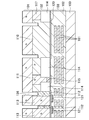
- FIG. 1 is a diagram schematically showing a cross section of a main part of the exemplary solid-state image sensor 100 according to the first embodiment of the present disclosure.
- the solid-state imaging device 100 includes an N-type semiconductor layer 101, an element layer 102 laminated on the N-type semiconductor layer 101 and including a photoelectric conversion element and an active element, and a wiring layer 103 further laminated on the N-type semiconductor layer 101 to perform wiring to the active element and the like. To be equipped.
- the incident light is incident on the element layer 102 from the side of the N-type semiconductor layer 101 opposite to the wiring layer 103.
- the N-type semiconductor layer 101 and the element layer 102 are formed by using an N-type epitaxial layer formed on an N-type semiconductor substrate (not shown).
- the device layer 102 is formed by forming the P-type and N-type regions and the insulating layer in the upper region of the N-type epitaxial layer.
- the region below the element layer 102 of the N-type epitaxial layer is the N-type semiconductor layer 101. This is an example, and the method for forming the N-type semiconductor layer 101 and the element layer 102 is not particularly limited.
- the element layer 102 includes a P-type well region 110, an N-type well region 111, a P-type layer 112, a photodiode 113 which is an N-type region, a high-concentration N-type layer 115, and a high-concentration P-type layer.
- 116 is provided by introducing impurities or the like.
- STI114 Shallow Trench Isolation
- the photodiode 113 performs photoelectric conversion with the incident light to generate a signal charge.
- the active element including the N-type well region 111 and the like converts the signal charge generated by the photodiode 113 into an electric signal and outputs the signal charge.
- a unit pixel is configured to include such a photodiode 113 and an active element.
- the unit pixels are arranged in a matrix to form a pixel array. Further, a circuit separated by a P-type well region and an N-type well region is formed in the peripheral portion of the pixel array.
- a wiring layer 103 including an insulating film 120 on the element and a transfer gate 121 formed on the insulating film 120 is formed.
- the N-type semiconductor layer 101 is provided with DTI135 (Deep Trench Isolation), which is an element separation groove that reaches the P-type layer 112 of the element layer 102 from the surface opposite to the element layer 102.
- the DTI 135 is formed by forming a groove 136 having a depth of penetrating the N-type semiconductor layer 101 and cutting a part of the element layer 102, and embedding the first insulating film 132 in the groove 136.
- the metal oxide film 131 made of hafnium oxide (HfO 2 ) or aluminum oxide (Al 2 O 3) covers the side wall and bottom surface of the groove 136. Is formed.
- the metal oxide film 131 is formed so as to cover the inside of the groove 136 and the surface of the N-type semiconductor layer 101. Therefore, the first insulating film 132 embeds the inside of the groove 136 via the metal oxide film 131. Further, the first insulating film 132 is formed so as to cover the metal oxide film 131 even outside the groove 136. Further, a second insulating film 133 is formed so as to cover the insulating film 132.
- a negative fixed charge is formed on the metal oxide film 131 on the side facing the N-type semiconductor layer 101 and the element layer 102.
- holes holes
- the hole accumulation layer 130 is formed. More specifically, the first hole storage layer 130a is formed along the surface of the N-type semiconductor layer 101 opposite to the element layer 102, and the second hole storage layer is formed on the bottom surface and the side wall of the groove 136. 130b is formed.
- a via 140 (through silicon via. TSV; Through-Silicon Via) that penetrates the N-type semiconductor layer 101 and the element layer 102 is formed.
- the via 140 is insulated from the N-type semiconductor layer 101 and the element layer 102 by a second insulating film 133.
- the copper wiring 122 is connected to the via 140 on the wiring layer 103 side, and the electrode pad 141 is connected on the N-type semiconductor layer 101 side.
- the P-type region (P-type layer 112, etc.) in the element layer 102 and the P-type region on the opposite side of the element layer 102 in the N-type semiconductor layer 101 is electrically connected to the second hole storage layer 130b formed along the DTI 135. Therefore, even when the thickness of the N-type semiconductor layer 101 is increased, holes are supplied through the second hole storage layer 130b formed on the side wall portion of the DTI 135, so that the increase in dark current is suppressed. be able to.
- FIG. 2 shows a solid-state image sensor 100a of a comparative example in which the DTI 135 is not formed in the solid-state image sensor 100.
- the solid-state image sensor 100a when the thickness T of the N-type semiconductor layer 101 is sufficiently small, a deep P-type well region is formed from the element layer 102 side by injecting impurities or the like, and the surface opposite to the element layer 102. It can be stretched to (back surface). In this case, it is possible to fix the potential of the P-type layer on the back surface side.
- the thickness T of the N-type semiconductor layer 101 is increased in order to improve the infrared sensitivity, it becomes difficult to form the P-type well region up to the back surface. As a result, the potential of the P-type layer on the back surface side cannot be fixed, and the dark current increases.
- the DTI 135 is formed from the back surface side, and the hole accumulation layer 130 is formed in the portion in contact with the DTI 135.
- the N-type semiconductor layer 101 becomes thick, holes can be supplied to the back surface side via the hole storage layer 130.
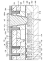
- FIG. 3 shows a schematic cross-sectional view of the solid-state image sensor 100b of the second embodiment.
- the solid-state image sensor 100b is the same as the solid-state image sensor 100 of FIG. 1 except that the via portion DTI135a is formed around the via 140.
- the via portion DTI135a has a configuration in which an insulating film is embedded in the groove via a metal oxide film 131, similarly to the DTI135 of the solid-state image sensor 100.
- FIG. 4 shows a schematic plan configuration A of the via 140 and the via portion DTI135a in the solid-state image sensor 100b as a plan view. As shown here, the via portion DTI135a is formed so as to surround the via 140.
- the via 140 is formed as a TSV penetrating the silicon substrate (N-type semiconductor layer 101) in order to form the electrode pad 141 on the side opposite to the element layer 102 in the N-type semiconductor layer 101.
- a pn junction is formed on the side surface of the DTI 135, which causes a leakage current.
- the via portion DTI135a is formed so as to surround the via 140.
- the N-type semiconductor layer 101a around the via 140 is electrically separated, so that the generation of leakage current is suppressed.
- the plane configuration B in FIG. 4 shows a modified example of the layout of the via portion DTI135a.
- the via portion DTI135a has a rectangular shape and has an angle that bends at 90 °.
- the shape (octagon) is such that the corner is bent at an obtuse angle (135 ° in this example) in two steps.
- the dimensions of the via portion DTI135a can be stabilized, and the embedding characteristics of the first insulating film 132 and the like when forming the via portion DTI135a can be stabilized.
- the shape of the via portion DTI135a in the plan view is not limited to the octagonal shape shown in the drawing, and may be another shape.
- FIG. 5 shows a schematic cross-sectional view of the exemplary solid-state image sensor 100c of the third embodiment. Comparing the solid-state image sensor 100c with the solid-state image sensor 100 of FIG. 1, the via 140, the copper wiring 122 connected to the via 140, and the electrode pad 141 are not formed. Further, a peripheral portion DTI135b having a structure similar to that of the DTI135 is formed.
- FIG. 6 shows, as a plan view, a peripheral portion DTI135b in the solid-state image sensor 100c and a schematic planar configuration C of an internal circuit region 151 surrounded by the peripheral portion DTI135b.
- An N-type well region and a P-type well region are both provided in the internal circuit region 151, and a photoelectric conversion element, an active element, and the like are configured.
- the left end of the solid-state image sensor 100c is the chip end 150 divided (diced) as a chip.
- the chip end 150 pn junctions are formed between the P-well layer 110 and the N-type semiconductor layer 101 and between the N-type semiconductor layer 101 and the hole-induced layer 130a. Also causes leakage current. Therefore, in the solid-state image sensor 100c, the peripheral portion DTI135b is formed along the chip end 150 at the peripheral portion of the chip. The peripheral edge DTI135b surrounds the inside without a break. As a result, the N-type semiconductor layer 101b near the chip end 150 is electrically separated, so that an increase in leakage current can be suppressed.
- the peripheral portion DTI135b is not provided with a portion that bends at 90 ° (obtuse angle, for example, a configuration that bends at 135 °). You can do it. This is shown in the plane configuration D of FIG. Thereby, the peripheral portion DTI135b can be stably formed.
- FIG. 7 shows a schematic cross-sectional view of the exemplary solid-state image sensor 100d of the fourth embodiment. Comparing the solid-state image sensor 100d with the solid-state image sensor 100c of FIG. 5, the difference is that the element layer 102 is provided with the end N-shaped well region 117 in the vicinity of the chip end 150. The end N-type well region 117 reaches the N-type semiconductor layer 101. In this way, the pn junction formed at the chip end 150 (diced surface) is reduced to only one location between the N-type semiconductor layer 101 and the hole-induced layer 130a, so that a leakage current is generated. Can be further suppressed.
- FIG. 8 shows, as a plan view, an end N-shaped well region 117 formed near the tip end 150, a P-shaped well region 110 provided inside the end portion N-shaped well region 110, and a P-shaped well region 110 along the tip end 150.
- the peripheral portion DTI135b provided and the internal circuit region 151 provided inside the peripheral portion DTI135b are shown.
- the peripheral edge portion DTI135b may be formed so as to bend at an obtuse angle (here, 135 °). This is shown as the plane configuration F in FIG.
- the configuration in which the N-type well region is provided on the element layer 102 so as to reach the N-type semiconductor layer 101 to reduce the pn junction can be applied to other than the vicinity of the chip end 150.
- the N-shaped well region as described above may be provided around the via 140 shown in FIG. 3 (not shown). As a result, the pn junction can be reduced around the via 140 and the leakage current can be suppressed.
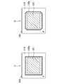
- FIG. 9 shows a schematic plan view of the exemplary solid-state image sensor 100e according to the fifth embodiment.
- FIG. 9 shows the entire chip of the solid-state image sensor 100e.
- a P-type well region 110, an N-type well region 111, and a via 140 are provided. Further, as described in the second embodiment (FIGS. 3 and 4), the via 140 and the via portion DTI135a surrounding the via 140 are provided. As a result, the leakage current is reduced around the via 140. Further, as described in the third embodiment (FIGS. 5 and 6), a peripheral edge portion DTI135b is provided along the chip end 150. As a result, the leakage current is reduced near the chip end 150.
- a pixel array 152 in which a plurality of unit pixels are arranged in a matrix is provided on the center side of the chip.
- An annular array portion DTI135c is formed so as to surround the pixel array 152.
- the array unit DTI135c has a structure similar to that of the DTI135 shown in FIG.
- the inside of the pixel array 152 and the peripheral portion can be electrically separated by using the P-type well region 110 and the array portion DTI135c. As a result, it is possible to suppress the influence of noise in the peripheral circuit on the pixel array 152 and the like.
- FIG. 10 shows the stage before forming DTI135.
- an N-type epitaxial layer is first formed on an N-type semiconductor substrate.
- a P-type well region 110, an N-type well region 111, a P-type layer 112, an N-type photodiode 113, and the like are formed in the upper region of the epitaxial layer by means such as impurity injection. It also forms STI 114.
- the pixel array 152 including the photoelectric conversion element, the active element, and the like is formed, and the epitaxial layer becomes the element layer 102.
- the region below the element layer 102 is the N-type semiconductor layer 101.
- a wiring layer 103 in which a plurality of wirings 161 are embedded in the insulating layer 162 is formed on the element layer 102. Further, another wafer is attached as the support substrate 160 on the wiring layer 103. Next, the thickness of the N-type semiconductor substrate used at the beginning is reduced and removed. If necessary, the N-type semiconductor layer 101 may also be thinned to a predetermined thickness. FIG. 10 shows this state with the support substrate 160 facing down.
- a groove 136 for forming the DTI 135 is formed.
- the groove 136 is formed so as to penetrate the N-type semiconductor layer 101 and scrape a part of the element layer 102.
- a groove 136 may be formed by creating a mask in which a predetermined position is opened by a technique in lithography and etching to a required depth.
- the metal oxide film 131 is formed so as to cover the bottom portion and the side wall of the groove 136 and also cover the N-type semiconductor layer 101 (on the surface opposite to the element layer 102). At this time, the space is left without completely filling the groove 136.
- the metal oxide film 131 is specifically an HfO 2 film or an Al 2 O 3 film, and is formed by, for example, a method such as CVD (Chemical Vapor Deposition).
- the metal oxide film 131 When the metal oxide film 131 is formed, holes are induced and accumulated in the portions of the N-type semiconductor layer 101 and the element layer 102 in contact with the metal oxide film 131, and the P-type hole accumulation layer 130 is formed. Therefore, the metal oxide film 131 is in a state of covering the inside of the groove 136 and the top of the N-type semiconductor layer 101 via the hole accumulation layer 130.
- the space left in the groove 136 is embedded, and the first insulating film 132 is formed so as to cover the metal oxide film 131 outside the groove 136.
- an oxide film may be formed as a material by a method such as CVD. As a result, DTI135 is formed.
- a through hole 140a for forming the via 140 is formed.
- the through hole 140a is formed so as to penetrate the N-type semiconductor layer 101 and the element layer 102, and partially scrape the first insulating film 132 and the insulating layer 162 of the wiring layer 103 to reach the wiring 161. ..
- etching or the like may be performed.
- the wiring 161 that the through hole 140a reaches corresponds to the copper wiring 122 in FIG.
- a second insulating film 133 is formed so as to cover the first insulating film 132 outside the through hole 140a together with the tail covering the side wall and the bottom surface of the through hole 140a. Then, at the bottom of the through hole 140a, the second insulating film 133 is partially removed to expose the wiring 161.
- the copper layer 140b is formed so as to embed the inside of the through hole 140a.
- the copper layer 140b is formed so as to cover the second insulating film even outside the through hole 140a.
- a plating method may be used for the formation of the copper layer 140b.
- the process of FIG. 16 will be described.
- the copper layer 140b in the outer portion of the through hole 140a is removed.
- the CMP method Chemical Mechanical Polishing
- the via 140 in which the through hole 140a is embedded by the copper layer 140b via the second insulating film 133 is formed.
- the electrode pad 141 connected to the via 140 is formed on the N-type semiconductor layer 101 side.
- the electrode pad 141 may be formed of, for example, aluminum.
- the solid-state image sensor of the present disclosure is manufactured.
- the materials, manufacturing methods, shapes, etc. described above are all examples, and the techniques of the present disclosure are not limited thereto.
- an increase in dark current can be suppressed even when the semiconductor layer is thickened, so that it is useful as a solid-state image sensor or the like with improved infrared sensitivity.
Abstract
This solid-state imaging device 100 is provided with: an N-type semiconductor layer 101; an element layer 102 which comprises a photoelectric conversion element and an active element; a wiring layer 103 which performs wiring to the active element; and an element isolation trench 135 which penetrates through the semiconductor layer 101. The element layer 102 comprises a P-type region 112 and an N-type region 113. A first hole accumulation layer 103a is formed on a surface of the semiconductor layer 101, said surface being on the reverse side from the element layer 102. A second hole accumulation layer 130b is formed on portions of the semiconductor layer 101 and the element layer 102, said portions being in contact with the element isolation trench 135. The P-type region 112 of the element layer 102 and the first hole accumulation layer 103a are connected to each other by means of the second hole accumulation layer 130b.
Description
本開示は、固体撮像装置に関する。
This disclosure relates to a solid-state image sensor.
近年、赤外領域の感度を大幅に高めたイメージセンサが多く提案されている。シリコンの赤外吸収感度は低いので、感度の向上のためには、赤外線がシリコン基板を透過する距離を延ばすことが有効である。そのことから、シリコン基板を厚く形成する技術が数多く提案されている。
In recent years, many image sensors with significantly improved sensitivity in the infrared region have been proposed. Since the infrared absorption sensitivity of silicon is low, it is effective to extend the distance through which infrared rays pass through the silicon substrate in order to improve the sensitivity. Therefore, many techniques for forming a thick silicon substrate have been proposed.
一方で、感度を向上する技術として、裏面照射型のイメージセンサが提案されている。これは、能動素子を形成する面とは反対側の面から光を入射させるイメージセンサである。これを開示する特許文献1によれば、裏面側の暗電流を抑制するために、裏面の表面にp型層を形成し、表面側から深いP型ウエルを介して電位固定する技術が開示されている。
On the other hand, a back-illuminated image sensor has been proposed as a technology for improving sensitivity. This is an image sensor that injects light from a surface opposite to the surface on which the active element is formed. According to Patent Document 1 which discloses this, in order to suppress a dark current on the back surface side, a technique of forming a p-type layer on the front surface of the back surface and fixing the potential from the front surface side through a deep P-type well is disclosed. ing.
しかしながら、赤外感度を向上するためにシリコン基板の厚みを増加させると、深いP型ウエル領域を裏面側まで延伸することが困難になる。この結果、裏面側のp型層を電位固定することができなくなり、暗電流が増加してしまう。
However, if the thickness of the silicon substrate is increased in order to improve the infrared sensitivity, it becomes difficult to extend the deep P-shaped well region to the back surface side. As a result, the potential of the p-type layer on the back surface side cannot be fixed, and the dark current increases.
以上に鑑み、本開示の技術は、赤外感度向上のために、裏面照射型のイメージセンサのシリコン基板の厚みを大きくしても、暗電流劣化のない、良好な画質を得ることが可能な撮像装置を提供することを目的とする。
In view of the above, the technique of the present disclosure can obtain good image quality without dark current deterioration even if the thickness of the silicon substrate of the back-illuminated image sensor is increased in order to improve the infrared sensitivity. It is an object of the present invention to provide an image pickup apparatus.
本開示の固体撮像装置は、複数の単位画素からなる画素アレイを有する固体撮像装置である。それぞれの単位画素は、光電変換により信号電荷を発生させる光電変換素子、及び、信号電荷を電気信号に変換すると共に出力する能動素子を含む。固体撮像装置は、N型の半導体層と、半導体層上に積層され、光電変換素子及び能動素子を含む素子層と、素子層上に積層され、能動素子に対して配線を行う配線層と、前記の半導体層を貫通する素子分離溝とを備える。素子層は、P型領域及びN型領域を含む。半導体層の素子層と反対側の面に、第1のホール蓄積層が形成されている。半導体層及び素子層の素子分離溝と接する部分に、第2のホール蓄積層が形成されている。素子層のP型領域と、第1のホール蓄積層とは、第2のホール蓄積層により接続されている。
The solid-state image sensor of the present disclosure is a solid-state image sensor having a pixel array composed of a plurality of unit pixels. Each unit pixel includes a photoelectric conversion element that generates a signal charge by photoelectric conversion, and an active element that converts the signal charge into an electric signal and outputs the signal charge. The solid-state imaging device includes an N-type semiconductor layer, an element layer laminated on the semiconductor layer and including a photoelectric conversion element and an active element, and a wiring layer laminated on the element layer and wiring to the active element. It is provided with an element separation groove penetrating the semiconductor layer. The device layer includes a P-type region and an N-type region. A first hole storage layer is formed on the surface of the semiconductor layer opposite to the element layer. A second hole storage layer is formed at a portion of the semiconductor layer and the element layer in contact with the element separation groove. The P-shaped region of the element layer and the first hole storage layer are connected by a second hole storage layer.
本開示の固体撮像装置によると、厚さが大きくなっても、暗電流の増加を抑制することができる。
According to the solid-state image sensor of the present disclosure, it is possible to suppress an increase in dark current even if the thickness is increased.
以下、本開示の各実施形態について、図面を参照して説明する。
Hereinafter, each embodiment of the present disclosure will be described with reference to the drawings.
(第1の実施形態)
図1は、本開示の第1の実施形態の例示的固体撮像装置100について、要部の断面を模式的に示す図である。 (First Embodiment)
FIG. 1 is a diagram schematically showing a cross section of a main part of the exemplary solid-state image sensor 100 according to the first embodiment of the present disclosure.
図1は、本開示の第1の実施形態の例示的固体撮像装置100について、要部の断面を模式的に示す図である。 (First Embodiment)
FIG. 1 is a diagram schematically showing a cross section of a main part of the exemplary solid-
固体撮像装置100は、N型半導体層101と、その上に積層され、光電変換素子及び能動素子を含む素子層102と、更にその上に積層され、能動素子等に対する配線を行う配線層103とを備える。固体撮像装置100において、入射光は、素子層102に対して配線層103とは反対側のN型半導体層101の側から入射する。
The solid-state imaging device 100 includes an N-type semiconductor layer 101, an element layer 102 laminated on the N-type semiconductor layer 101 and including a photoelectric conversion element and an active element, and a wiring layer 103 further laminated on the N-type semiconductor layer 101 to perform wiring to the active element and the like. To be equipped. In the solid-state image sensor 100, the incident light is incident on the element layer 102 from the side of the N-type semiconductor layer 101 opposite to the wiring layer 103.
N型半導体層101及び素子層102は、N型半導体基板(図示せず)上に形成したN型のエピタキシャル層を用いて形成される。当該N型のエピタキシャル層の上部の領域に、P型及びN型の領域と、絶縁層とを形成することにより、素子層102が形成される。N型のエピタキシャル層の素子層102よりも下方の領域は、N型半導体層101となる。尚、これは一例であり、N型半導体層101及び素子層102の形成方法について、特に限定はされない。
The N-type semiconductor layer 101 and the element layer 102 are formed by using an N-type epitaxial layer formed on an N-type semiconductor substrate (not shown). The device layer 102 is formed by forming the P-type and N-type regions and the insulating layer in the upper region of the N-type epitaxial layer. The region below the element layer 102 of the N-type epitaxial layer is the N-type semiconductor layer 101. This is an example, and the method for forming the N-type semiconductor layer 101 and the element layer 102 is not particularly limited.
素子層102は、より具体的には、P型ウエル領域110、N型ウエル領域111、P型層112、N型の領域であるフォトダイオード113、高濃度N型層115及び高濃度P型層116について、不純物の導入等により設けられている。更に、N型半導体層101を貫通し、且つ、素子層102の一部を除去するように溝を形成すると共に、当該溝に不純物を埋め込むことにより、素子分離溝であるSTI114(Shallow Trench Isolation)が設けられている。
More specifically, the element layer 102 includes a P-type well region 110, an N-type well region 111, a P-type layer 112, a photodiode 113 which is an N-type region, a high-concentration N-type layer 115, and a high-concentration P-type layer. 116 is provided by introducing impurities or the like. Further, by forming a groove so as to penetrate the N-type semiconductor layer 101 and remove a part of the element layer 102 and embedding impurities in the groove, STI114 (Shallow Trench Isolation), which is an element separation groove, is formed. Is provided.
フォトダイオード113は、入射した光により光電変換を行い、信号電荷を発生させる。N型ウエル領域111等を含む能動素子は、フォトダイオード113が発生させた信号電荷を電気信号に変換し、且つ、出力する。このようなフォトダイオード113及び能動素子を含むように、単位画素が構成される。当該単位画素は行列状に配置されて、画素アレイを構成している。また、画素アレイの周辺部には、P型ウエル領域及びN型ウエル領域により分離された回路が形成されている。
The photodiode 113 performs photoelectric conversion with the incident light to generate a signal charge. The active element including the N-type well region 111 and the like converts the signal charge generated by the photodiode 113 into an electric signal and outputs the signal charge. A unit pixel is configured to include such a photodiode 113 and an active element. The unit pixels are arranged in a matrix to form a pixel array. Further, a circuit separated by a P-type well region and an N-type well region is formed in the peripheral portion of the pixel array.
素子層102上には、素子上絶縁膜120及びその上に形成された転送ゲート121を含む配線層103が形成されている。
On the element layer 102, a wiring layer 103 including an insulating film 120 on the element and a transfer gate 121 formed on the insulating film 120 is formed.
また、N型半導体層101に対して、素子層102とは反対側の面から素子層102のP型層112に達する素子分離溝であるDTI135(Deep Trench Isolation)が設けられている。DTI135は、N型半導体層101を貫通して素子層102の一部を削る深さの溝136を形成し、溝136内に第1の絶縁膜132を埋め込むことにより形成される。
Further, the N-type semiconductor layer 101 is provided with DTI135 (Deep Trench Isolation), which is an element separation groove that reaches the P-type layer 112 of the element layer 102 from the surface opposite to the element layer 102. The DTI 135 is formed by forming a groove 136 having a depth of penetrating the N-type semiconductor layer 101 and cutting a part of the element layer 102, and embedding the first insulating film 132 in the groove 136.
但し、第1の絶縁膜132が埋め込まれるよりも前に、溝136の側壁及び底面を覆うように、ハフニウム酸化物(HfO2)又はアルミニウム酸化物(Al2O3)からなる金属酸化膜131が形成されている。
However, before the first insulating film 132 is embedded, the metal oxide film 131 made of hafnium oxide (HfO 2 ) or aluminum oxide (Al 2 O 3) covers the side wall and bottom surface of the groove 136. Is formed.
金属酸化膜131は、溝136の内側を覆うと共に、N型半導体層101の表面を覆うように形成されている。従って、第1の絶縁膜132は、金属酸化膜131を介して溝136の内側を埋め込んでいる。また、第1の絶縁膜132は、溝136の外においても、金属酸化膜131を覆うように形成されている。更に、絶縁膜132を覆うように、第2の絶縁膜133が形成されている。
The metal oxide film 131 is formed so as to cover the inside of the groove 136 and the surface of the N-type semiconductor layer 101. Therefore, the first insulating film 132 embeds the inside of the groove 136 via the metal oxide film 131. Further, the first insulating film 132 is formed so as to cover the metal oxide film 131 even outside the groove 136. Further, a second insulating film 133 is formed so as to cover the insulating film 132.
金属酸化膜131には、N型半導体層101及び素子層102に面する側に、負の固定電荷が形成される。これにより、N型半導体層101及び素子層102において、金属酸化膜131と接する部分には、GND端子からP型ウエル層110を介してホール(正孔)が供給され、蓄積されてP型となったホール蓄積層130が形成される。より詳しくは、N型半導体層101における素子層102と反対側の面に沿って第1のホール蓄積層130aが形成されると共に、溝136の底面及び側壁の部分には第2のホール蓄積層130bが形成される。
A negative fixed charge is formed on the metal oxide film 131 on the side facing the N-type semiconductor layer 101 and the element layer 102. As a result, holes (holes) are supplied from the GND terminal to the portions of the N-type semiconductor layer 101 and the element layer 102 in contact with the metal oxide film 131 via the P-type well layer 110, and are accumulated to form the P-type. The hole accumulation layer 130 is formed. More specifically, the first hole storage layer 130a is formed along the surface of the N-type semiconductor layer 101 opposite to the element layer 102, and the second hole storage layer is formed on the bottom surface and the side wall of the groove 136. 130b is formed.
また、N型半導体層101及び素子層102を貫通するビア140(シリコン貫通電極。TSV;Through-Silicon Via)が形成されている。ビア140は、N型半導体層101及び素子層102とは第2の絶縁膜133によって絶縁されている。また、ビア140に対して、配線層103の側では銅配線122が接続され、且つ、N型半導体層101側では電極パッド141が接続されている。
Further, a via 140 (through silicon via. TSV; Through-Silicon Via) that penetrates the N-type semiconductor layer 101 and the element layer 102 is formed. The via 140 is insulated from the N-type semiconductor layer 101 and the element layer 102 by a second insulating film 133. Further, the copper wiring 122 is connected to the via 140 on the wiring layer 103 side, and the electrode pad 141 is connected on the N-type semiconductor layer 101 side.
以上のような本開示の固体撮像装置100において、素子層102におけるP型の領域(P型層112等)と、N型半導体層101における素子層102とは反対側のP型の領域である第1のホール蓄積層130aとは、DTI135に沿って形成された第2のホール蓄積層130bによって電気的に接続される。従って、N型半導体層101の厚さが大きくなった場合にも、DTI135の側壁部分に形成される第2のホール蓄積層130bを介してホールが供給されるので、暗電流の増加を抑制することができる。
In the solid-state imaging device 100 of the present disclosure as described above, the P-type region (P-type layer 112, etc.) in the element layer 102 and the P-type region on the opposite side of the element layer 102 in the N-type semiconductor layer 101. The first hole storage layer 130a is electrically connected to the second hole storage layer 130b formed along the DTI 135. Therefore, even when the thickness of the N-type semiconductor layer 101 is increased, holes are supplied through the second hole storage layer 130b formed on the side wall portion of the DTI 135, so that the increase in dark current is suppressed. be able to.
図2には、固体撮像装置100におけるDTI135が形成されていない構成である比較例の固体撮像装置100aを示す。固体撮像装置100aにおいて、N型半導体層101の厚さTが十分に小さい場合には、素子層102側から不純物注入等により深いP型ウエル領域を形成し、素子層102とは反対側の面(裏面)まで延伸させることができる。この場合は、裏面側のP型層の電位を固定することは可能である。
FIG. 2 shows a solid-state image sensor 100a of a comparative example in which the DTI 135 is not formed in the solid-state image sensor 100. In the solid-state image sensor 100a, when the thickness T of the N-type semiconductor layer 101 is sufficiently small, a deep P-type well region is formed from the element layer 102 side by injecting impurities or the like, and the surface opposite to the element layer 102. It can be stretched to (back surface). In this case, it is possible to fix the potential of the P-type layer on the back surface side.
しかしながら、赤外感度を向上させるためにN型半導体層101の厚さTを大きくすると、裏面までP型ウエル領域を形成することは困難となる。この結果、裏面側のP型層の電位を固定することができなくなり、暗電流が増加する。
However, if the thickness T of the N-type semiconductor layer 101 is increased in order to improve the infrared sensitivity, it becomes difficult to form the P-type well region up to the back surface. As a result, the potential of the P-type layer on the back surface side cannot be fixed, and the dark current increases.
これに対して、図1に示す本開示の固体撮像装置100では、裏面側からDTI135が形成され、当該DTI135に接する部分にホール蓄積層130が形成されている。これにより、N型半導体層101が厚くなった場合にも、ホール蓄積層130を介して裏面側にホールを供給することができる。この結果、暗電流の増加を抑制し、撮像される画像の質を向上することができる。
On the other hand, in the solid-state image sensor 100 of the present disclosure shown in FIG. 1, the DTI 135 is formed from the back surface side, and the hole accumulation layer 130 is formed in the portion in contact with the DTI 135. As a result, even when the N-type semiconductor layer 101 becomes thick, holes can be supplied to the back surface side via the hole storage layer 130. As a result, it is possible to suppress an increase in dark current and improve the quality of the captured image.
(第2の実施形態)
図3に、第2の実施形態の固体撮像装置100bについて模式的な断面図を示す。固体撮像装置100bは、ビア140の周囲にビア部DTI135aが形成されている他は、図1の固体撮像装置100と同様である。ビア部DTI135aは、固体撮像装置100のDTI135と同様に、溝に金属酸化膜131を介して絶縁膜が埋め込まれた構成である。 (Second Embodiment)
FIG. 3 shows a schematic cross-sectional view of the solid-state image sensor 100b of the second embodiment. The solid-state image sensor 100b is the same as the solid-state image sensor 100 of FIG. 1 except that the via portion DTI135a is formed around the via 140. The via portion DTI135a has a configuration in which an insulating film is embedded in the groove via a metal oxide film 131, similarly to the DTI135 of the solid-state image sensor 100.
図3に、第2の実施形態の固体撮像装置100bについて模式的な断面図を示す。固体撮像装置100bは、ビア140の周囲にビア部DTI135aが形成されている他は、図1の固体撮像装置100と同様である。ビア部DTI135aは、固体撮像装置100のDTI135と同様に、溝に金属酸化膜131を介して絶縁膜が埋め込まれた構成である。 (Second Embodiment)
FIG. 3 shows a schematic cross-sectional view of the solid-
また、図4には、平面図として、固体撮像装置100bにおけるビア140及びビア部DTI135aの模式的な平面構成Aを示す。ここに示される通り、ビア部DTI135aは、ビア140の周囲を取り囲むように形成されている。
Further, FIG. 4 shows a schematic plan configuration A of the via 140 and the via portion DTI135a in the solid-state image sensor 100b as a plan view. As shown here, the via portion DTI135a is formed so as to surround the via 140.
ビア140は、N型半導体層101において、素子層102とは反対側に電極パッド141を形成するために、シリコン基板(N型半導体層101)を貫通するTSVとして形成される。DTI135の側面において、p-n接合が形成されており、これはリーク電流が発生する原因となる。
The via 140 is formed as a TSV penetrating the silicon substrate (N-type semiconductor layer 101) in order to form the electrode pad 141 on the side opposite to the element layer 102 in the N-type semiconductor layer 101. A pn junction is formed on the side surface of the DTI 135, which causes a leakage current.
そこで、本実施形態の固体撮像装置100bでは、ビア140を取り囲むようにビア部DTI135aを形成している。これにより、ビア140の周辺のN型半導体層101aが電気的に分離されるので、リーク電流の発生が抑制される。
Therefore, in the solid-state image sensor 100b of the present embodiment, the via portion DTI135a is formed so as to surround the via 140. As a result, the N-type semiconductor layer 101a around the via 140 is electrically separated, so that the generation of leakage current is suppressed.
尚、図4の平面構成Bは、ビア部DTI135aのレイアウトの変形例を示す。平面構成Aでは、ビア部DTI135aは長方形状であり、90°に曲がる角を有している。これに対し、平面構成Bでは、長方形の角において90°に曲がる代わりに、鈍角(この例では135°)に2回に分けて曲がるようにした形状(八角形)である。このように、90°に曲がる部分を設けない構成とすることにより、ビア部DTI135aの寸法が安定し、ビア部DTI135aを形成する際の第1の絶縁膜132等の埋め込み特性を安定させることができる。尚、ビア部DTI135aの平面図における形状について、図示した八角形には限らず、他の形状であっても良い。
Note that the plane configuration B in FIG. 4 shows a modified example of the layout of the via portion DTI135a. In the plane configuration A, the via portion DTI135a has a rectangular shape and has an angle that bends at 90 °. On the other hand, in the plane configuration B, instead of bending at a rectangular corner of 90 °, the shape (octagon) is such that the corner is bent at an obtuse angle (135 ° in this example) in two steps. In this way, by providing a configuration that does not provide a portion that bends at 90 °, the dimensions of the via portion DTI135a can be stabilized, and the embedding characteristics of the first insulating film 132 and the like when forming the via portion DTI135a can be stabilized. can. The shape of the via portion DTI135a in the plan view is not limited to the octagonal shape shown in the drawing, and may be another shape.
(第3の実施形態)
図5に、第3の実施形態の例示的固体撮像装置100cについて模式的な断面図を示す。固体撮像装置100cを図1の固体撮像装置100と比較すると、ビア140と、これに接続される銅配線122及び電極パッド141が形成されていない。また、DTI135と同様の構造を有する周縁部DTI135bが形成されている。 (Third Embodiment)
FIG. 5 shows a schematic cross-sectional view of the exemplary solid-state image sensor 100c of the third embodiment. Comparing the solid-state image sensor 100c with the solid-state image sensor 100 of FIG. 1, the via 140, the copper wiring 122 connected to the via 140, and the electrode pad 141 are not formed. Further, a peripheral portion DTI135b having a structure similar to that of the DTI135 is formed.
図5に、第3の実施形態の例示的固体撮像装置100cについて模式的な断面図を示す。固体撮像装置100cを図1の固体撮像装置100と比較すると、ビア140と、これに接続される銅配線122及び電極パッド141が形成されていない。また、DTI135と同様の構造を有する周縁部DTI135bが形成されている。 (Third Embodiment)
FIG. 5 shows a schematic cross-sectional view of the exemplary solid-
また、図6には、平面図として、固体撮像装置100cにおける周縁部DTI135bと、これに囲まれた内部回路領域151の模式的な平面構成Cを示す。内部回路領域151には、N型ウエル領域及びP型ウエル領域が共に設けられ、光電変換素子、能動素子等が構成されている。
Further, FIG. 6 shows, as a plan view, a peripheral portion DTI135b in the solid-state image sensor 100c and a schematic planar configuration C of an internal circuit region 151 surrounded by the peripheral portion DTI135b. An N-type well region and a P-type well region are both provided in the internal circuit region 151, and a photoelectric conversion element, an active element, and the like are configured.
図5において、固体撮像装置100cの左端は、チップとして分割(ダイシング)したチップ端150である。チップ端150には、Pウエル層110とN型半導体層101との間、及び、N型半導体層101とホール誘起層130aとの間の2ヶ所にp-n接合が形成されており、これもリーク電流の原因となる。そこで、固体撮像装置100cでは、チップ周縁部において、チップ端150に沿って周縁部DTI135bが形成されている。周縁部DTI135bは、切れ目無く内側を取り囲んでいる。これにより、チップ端150付近のN型半導体層101bが電気的に分離されるので、リーク電流の増加を抑制することができる。
In FIG. 5, the left end of the solid-state image sensor 100c is the chip end 150 divided (diced) as a chip. At the chip end 150, pn junctions are formed between the P-well layer 110 and the N-type semiconductor layer 101 and between the N-type semiconductor layer 101 and the hole-induced layer 130a. Also causes leakage current. Therefore, in the solid-state image sensor 100c, the peripheral portion DTI135b is formed along the chip end 150 at the peripheral portion of the chip. The peripheral edge DTI135b surrounds the inside without a break. As a result, the N-type semiconductor layer 101b near the chip end 150 is electrically separated, so that an increase in leakage current can be suppressed.
尚、変形例として、図4の平面構成Bに示したビア部DTI135aと同様に、周縁部DTI135bについても、90°に曲がる部分を設けない(鈍角、一例として135°に曲がる構成とする)ようにしても良い。これを図6の平面構成Dに示す。これにより、周縁部DTI135bを安定して形成することができる。
As a modified example, similarly to the via portion DTI135a shown in the plane configuration B of FIG. 4, the peripheral portion DTI135b is not provided with a portion that bends at 90 ° (obtuse angle, for example, a configuration that bends at 135 °). You can do it. This is shown in the plane configuration D of FIG. Thereby, the peripheral portion DTI135b can be stably formed.
(第4の実施形態)
図7に、第4の実施形態の例示的固体撮像装置100dについて模式的な断面図を示す。固体撮像装置100dを図5の固体撮像装置100cと比較すると、チップ端150付近において、素子層102に端部N型ウエル領域117が設けられている点が異なる。端部N型ウエル領域117は、N型半導体層101に達している。このようにすると、チップ端150(ダイシングされた面)に形成されるp-n接合がN型半導体層101とホール誘起層130aの間の1ヶ所のみとなって少なくなるので、リーク電流の発生を更に抑制することができる。 (Fourth Embodiment)
FIG. 7 shows a schematic cross-sectional view of the exemplary solid-state image sensor 100d of the fourth embodiment. Comparing the solid-state image sensor 100d with the solid-state image sensor 100c of FIG. 5, the difference is that the element layer 102 is provided with the end N-shaped well region 117 in the vicinity of the chip end 150. The end N-type well region 117 reaches the N-type semiconductor layer 101. In this way, the pn junction formed at the chip end 150 (diced surface) is reduced to only one location between the N-type semiconductor layer 101 and the hole-induced layer 130a, so that a leakage current is generated. Can be further suppressed.
図7に、第4の実施形態の例示的固体撮像装置100dについて模式的な断面図を示す。固体撮像装置100dを図5の固体撮像装置100cと比較すると、チップ端150付近において、素子層102に端部N型ウエル領域117が設けられている点が異なる。端部N型ウエル領域117は、N型半導体層101に達している。このようにすると、チップ端150(ダイシングされた面)に形成されるp-n接合がN型半導体層101とホール誘起層130aの間の1ヶ所のみとなって少なくなるので、リーク電流の発生を更に抑制することができる。 (Fourth Embodiment)
FIG. 7 shows a schematic cross-sectional view of the exemplary solid-
図8には、平面図として、チップ端150付近に形成された端部N型ウエル領域117、その内側に設けられたP型ウエル領域110、チップ端150に沿ってP型ウエル領域110内に設けられた周縁部DTI135b、及び、周縁部DTI135bよりも内側に設けられた内部回路領域151を示す。また、変形例として、図4の平面構成Bの場合と同様に、周縁部DTI135bが鈍角(ここでは135°)に曲がるように形成しても良い。これを図8の平面構成Fとして示す。
FIG. 8 shows, as a plan view, an end N-shaped well region 117 formed near the tip end 150, a P-shaped well region 110 provided inside the end portion N-shaped well region 110, and a P-shaped well region 110 along the tip end 150. The peripheral portion DTI135b provided and the internal circuit region 151 provided inside the peripheral portion DTI135b are shown. Further, as a modification, as in the case of the plane configuration B in FIG. 4, the peripheral edge portion DTI135b may be formed so as to bend at an obtuse angle (here, 135 °). This is shown as the plane configuration F in FIG.
更に、素子層102に対し、N型半導体層101に達するようにN型ウエル領域を設けてp-n接合を減らす構成は、チップ端150付近以外にも適用できる。例えば、図3に示すビア140周辺において、上記のようなN型ウエル領域を設けても良い(図示は省略)。これにより、ビア140周辺においてp-n接合を削減し、リーク電流を抑制することができる。
Further, the configuration in which the N-type well region is provided on the element layer 102 so as to reach the N-type semiconductor layer 101 to reduce the pn junction can be applied to other than the vicinity of the chip end 150. For example, the N-shaped well region as described above may be provided around the via 140 shown in FIG. 3 (not shown). As a result, the pn junction can be reduced around the via 140 and the leakage current can be suppressed.
(第5の実施形態)
図9に、第5の実施形態の例示的固体撮像装置100eの模式的な平面図を示す。図9は、固体撮像装置100eのチップ全体を示している。 (Fifth Embodiment)
FIG. 9 shows a schematic plan view of the exemplary solid-state image sensor 100e according to the fifth embodiment. FIG. 9 shows the entire chip of the solid-state image sensor 100e.
図9に、第5の実施形態の例示的固体撮像装置100eの模式的な平面図を示す。図9は、固体撮像装置100eのチップ全体を示している。 (Fifth Embodiment)
FIG. 9 shows a schematic plan view of the exemplary solid-
図9において、P型ウエル領域110、N型ウエル領域111及びビア140が設けられている。また、第2の実施形態(図3及び図4)にて説明したように、ビア140及びこれを囲むビア部DTI135aが設けられている。これにより、ビア140周辺においてリーク電流が低減される。また、第3の実施形態(図5及び図6)にて説明したように、チップ端150に沿って周縁部DTI135bが設けられている。これにより、チップ端150付近においてリーク電流が低減される。
In FIG. 9, a P-type well region 110, an N-type well region 111, and a via 140 are provided. Further, as described in the second embodiment (FIGS. 3 and 4), the via 140 and the via portion DTI135a surrounding the via 140 are provided. As a result, the leakage current is reduced around the via 140. Further, as described in the third embodiment (FIGS. 5 and 6), a peripheral edge portion DTI135b is provided along the chip end 150. As a result, the leakage current is reduced near the chip end 150.
また、固体撮像装置100eにおいて、チップの中央側に、複数の単位画素が行列状に配置された画素アレイ152が設けられている。画素アレイ152を囲むように、環状のアレイ部DTI135cが形成されている。アレイ部DTI135cは、図1に示すDTI135等と同様の構造を有する。
Further, in the solid-state image sensor 100e, a pixel array 152 in which a plurality of unit pixels are arranged in a matrix is provided on the center side of the chip. An annular array portion DTI135c is formed so as to surround the pixel array 152. The array unit DTI135c has a structure similar to that of the DTI135 shown in FIG.
P型ウエル領域110及びアレイ部DTI135cを利用して、画素アレイ152内と、周辺部とを電気的に分離することができる。この結果、周辺回路のノイズが画素アレイ152に影響する等を抑制することができる。
The inside of the pixel array 152 and the peripheral portion can be electrically separated by using the P-type well region 110 and the array portion DTI135c. As a result, it is possible to suppress the influence of noise in the peripheral circuit on the pixel array 152 and the like.
(第6の実施例)
次に、第6の実施形態として、固体撮像装置の製造方法を説明する。特に、DTI135の製造方法について詳しく説明する。図10~図17は、本開示の固体撮像装置の製造方法を説明する図である。尚、これらの図において、固体撮像装置は、図1等とは上下を逆に示している。 (Sixth Example)
Next, as a sixth embodiment, a method of manufacturing a solid-state image sensor will be described. In particular, the manufacturing method of DTI135 will be described in detail. 10 to 17 are views for explaining the manufacturing method of the solid-state image sensor of the present disclosure. In these figures, the solid-state image sensor is shown upside down from FIG. 1 and the like.
図10は、DTI135を形成する前の段階を示している。この構造を得るために、初めに、N型の半導体基板上に、N型のエピタキシャル層を形成する。当該エピタキシャル層の上部の領域に対し、不純物注入等の手段を用いて、P型ウエル領域110、N型ウエル領域111、P型層112及びN型のフォトダイオード113等を形成する。また、STI114も形成する。これにより、光電変換素子及び能動素子等を備える画素アレイ152が形成され、前記エピタキシャル層が素子層102となる。前記のN型のエピタキシャル層のうち、素子層102よりも下方の領域は、N型半導体層101となる。
FIG. 10 shows the stage before forming DTI135. In order to obtain this structure, an N-type epitaxial layer is first formed on an N-type semiconductor substrate. A P-type well region 110, an N-type well region 111, a P-type layer 112, an N-type photodiode 113, and the like are formed in the upper region of the epitaxial layer by means such as impurity injection. It also forms STI 114. As a result, the pixel array 152 including the photoelectric conversion element, the active element, and the like is formed, and the epitaxial layer becomes the element layer 102. Of the N-type epitaxial layer, the region below the element layer 102 is the N-type semiconductor layer 101.
続いて、素子層102上に、絶縁層162内に複数の配線161が埋め込まれた配線層103を形成する。更に、配線層103上に、別のウエハを支持基板160として貼り付ける。次に、初めに用いたN型の半導体基板の厚さを薄くして、除去する。尚、必要に応じてN型半導体層101についても薄くして、所定の厚さとしても良い。図10は、この状態について、支持基板160を下にして示したものである。
Subsequently, on the element layer 102, a wiring layer 103 in which a plurality of wirings 161 are embedded in the insulating layer 162 is formed. Further, another wafer is attached as the support substrate 160 on the wiring layer 103. Next, the thickness of the N-type semiconductor substrate used at the beginning is reduced and removed. If necessary, the N-type semiconductor layer 101 may also be thinned to a predetermined thickness. FIG. 10 shows this state with the support substrate 160 facing down.
次に、図11の工程を行う。ここでは、DTI135を形成するための溝136を形成する。溝136は、N型半導体層101を貫通し且つ素子層102の一部を削るように形成する。例えば、リソグラフィーに技術より所定の位置が開口されたマスクを作成し、必要な深さまでエッチングすることにより溝136を形成しても良い。
Next, the process shown in FIG. 11 is performed. Here, a groove 136 for forming the DTI 135 is formed. The groove 136 is formed so as to penetrate the N-type semiconductor layer 101 and scrape a part of the element layer 102. For example, a groove 136 may be formed by creating a mask in which a predetermined position is opened by a technique in lithography and etching to a required depth.
次に、図12の工程を行う。ここでは、溝136の底部及び側壁を覆うと共に、N型半導体層101上(素子層102と反対側の面上)を覆うように、金属酸化膜131を形成する。この際、溝136を完全に満たすことなく、空間を残すようにする。金属酸化膜131は、具体的にはHfO2膜又はAl2O3膜であり、例えばCVD(Chemical Vapor Deposition、化学気相成長)等の方法により形成する。
Next, the step of FIG. 12 is performed. Here, the metal oxide film 131 is formed so as to cover the bottom portion and the side wall of the groove 136 and also cover the N-type semiconductor layer 101 (on the surface opposite to the element layer 102). At this time, the space is left without completely filling the groove 136. The metal oxide film 131 is specifically an HfO 2 film or an Al 2 O 3 film, and is formed by, for example, a method such as CVD (Chemical Vapor Deposition).
金属酸化膜131が形成されると、N型半導体層101及び素子層102の金属酸化膜131と接する部分において、ホールが誘起されて蓄積し、P型のホール蓄積層130が形成される。従って、金属酸化膜131は、ホール蓄積層130を介して溝136内及びN型半導体層101上を覆う状態となる。
When the metal oxide film 131 is formed, holes are induced and accumulated in the portions of the N-type semiconductor layer 101 and the element layer 102 in contact with the metal oxide film 131, and the P-type hole accumulation layer 130 is formed. Therefore, the metal oxide film 131 is in a state of covering the inside of the groove 136 and the top of the N-type semiconductor layer 101 via the hole accumulation layer 130.
次に、図13の工程を説明する。ここでは、溝136内に残された空間を埋め込むと共に、溝136の外において金属酸化膜131を覆うように、第1の絶縁膜132を形成する。例えば、CVD等の方法により、酸化膜を材料として形成しても良い。これにより、DTI135が形成されたことになる。
Next, the process of FIG. 13 will be described. Here, the space left in the groove 136 is embedded, and the first insulating film 132 is formed so as to cover the metal oxide film 131 outside the groove 136. For example, an oxide film may be formed as a material by a method such as CVD. As a result, DTI135 is formed.
次に、図14の工程を説明する。ここでは、ビア140を形成するための貫通孔140aを形成する。貫通孔140aは、N型半導体層101及び素子層102を貫通し、且つ、配線層103のうちの第1の絶縁膜132及び絶縁層162を部分的に削り、配線161に達するように形成する。このためには、例えばエッチング等を行えば良い。貫通孔140aが達する配線161は、図1における銅配線122に対応する。
Next, the process of FIG. 14 will be described. Here, a through hole 140a for forming the via 140 is formed. The through hole 140a is formed so as to penetrate the N-type semiconductor layer 101 and the element layer 102, and partially scrape the first insulating film 132 and the insulating layer 162 of the wiring layer 103 to reach the wiring 161. .. For this purpose, for example, etching or the like may be performed. The wiring 161 that the through hole 140a reaches corresponds to the copper wiring 122 in FIG.
更に、貫通孔140aの側壁及び底面を覆う尾と共に、貫通孔140aの外において第1の絶縁膜132を覆うように、第2の絶縁膜133を形成する。その後、貫通孔140aの底部において、第2の絶縁膜133を一部除去して配線161を露出させる。
Further, a second insulating film 133 is formed so as to cover the first insulating film 132 outside the through hole 140a together with the tail covering the side wall and the bottom surface of the through hole 140a. Then, at the bottom of the through hole 140a, the second insulating film 133 is partially removed to expose the wiring 161.
次に、図15の工程を説明する。ここでは、ビア140を形成するために、貫通孔140a内を埋め込むように銅層140bを形成する。銅層140bは、貫通孔140aの外においても第2の絶縁膜上を覆うように形成される。銅層140bの形成には、例えばメッキ法を用いても良い。
Next, the process of FIG. 15 will be described. Here, in order to form the via 140, the copper layer 140b is formed so as to embed the inside of the through hole 140a. The copper layer 140b is formed so as to cover the second insulating film even outside the through hole 140a. For the formation of the copper layer 140b, for example, a plating method may be used.
次に、図16の工程を説明する。ここでは、貫通孔140aの外の部分の銅層140bを除去する。このためには、例えばCMP法(化学機械研磨:Chemical Mechanical Polishing)を用いても良い。これにより、貫通孔140aが第2の絶縁膜133を介して銅層140bによって埋め込まれたビア140が形成されたことになる。
Next, the process of FIG. 16 will be described. Here, the copper layer 140b in the outer portion of the through hole 140a is removed. For this purpose, for example, the CMP method (Chemical Mechanical Polishing) may be used. As a result, the via 140 in which the through hole 140a is embedded by the copper layer 140b via the second insulating film 133 is formed.
次に、図17の工程を説明する。ここでは、N型半導体層101側においてビア140に接続する電極パッド141を形成する。電極パッド141は、例えばアルミニウムにより形成してもよい。
Next, the process of FIG. 17 will be described. Here, the electrode pad 141 connected to the via 140 is formed on the N-type semiconductor layer 101 side. The electrode pad 141 may be formed of, for example, aluminum.
以上により、本開示の固体撮像装置が製造される。尚、以上に記載した材料、製造方法、形状等はいずれも例示であり、本開示の技術はこれらに限定されることはない。
From the above, the solid-state image sensor of the present disclosure is manufactured. The materials, manufacturing methods, shapes, etc. described above are all examples, and the techniques of the present disclosure are not limited thereto.
本開示の固体撮像装置によると、半導体層を厚くした場合にも暗電流の増加を抑制することができるので、赤外感度を向上させた固体撮像装置等として有用である。
According to the solid-state image sensor of the present disclosure, an increase in dark current can be suppressed even when the semiconductor layer is thickened, so that it is useful as a solid-state image sensor or the like with improved infrared sensitivity.
100 固体撮像装置
100a~100e 固体撮像装置
101 N型半導体層
101a N型半導体層
101b N型半導体層
102 素子層
103 配線層
110 P型ウエル領域
111 N型ウエル領域
112 P型層
113 フォトダイオード
114 STI
115 高濃度N型層
116 高濃度P型層
117 端部Nウエル領域
120 素子上絶縁膜
121 電極
122 銅配線
130 ホール蓄積層
130a 第1のホール蓄積層
130b 第2のホール蓄積層
131 金属酸化膜
132 第1の絶縁膜
133 第2の絶縁膜
135 DTI
135a ビア部DTI
135b 周縁部DTI
135c アレイ部DTI
136 溝
140 ビア
140a 貫通孔
140b 銅層
141 電極パッド
150 チップ端
151 内部回路領域
152 画素アレイ
160 支持基板
161 配線
162 絶縁層 100 Solid-type imaging device 100a to 100e Solid-type imaging device 101 N-type semiconductor layer 101a N-type semiconductor layer 101b N-type semiconductor layer 102 Element layer 103 Wiring layer 110 P-type well region 111 N-type well region 112 P-type layer 113 Photodiode 114 STI
115 High-concentration N-type layer 116 High-concentration P-type layer 117 End N-well region 120 Insulating film on element 121 Electrode 122 Copper wiring 130 Hole storage layer 130a First hole storage layer 130b Second hole storage layer 131 Metal oxide film 132 First insulating film 133 Second insulating film 135 DTI
135a Via part DTI
135b Peripheral DTI
135c Array section DTI
136Groove 140 Via 140a Through hole 140b Copper layer 141 Electrode pad 150 Chip end 151 Internal circuit area 152 Pixel array 160 Support board 161 Wiring 162 Insulation layer
100a~100e 固体撮像装置
101 N型半導体層
101a N型半導体層
101b N型半導体層
102 素子層
103 配線層
110 P型ウエル領域
111 N型ウエル領域
112 P型層
113 フォトダイオード
114 STI
115 高濃度N型層
116 高濃度P型層
117 端部Nウエル領域
120 素子上絶縁膜
121 電極
122 銅配線
130 ホール蓄積層
130a 第1のホール蓄積層
130b 第2のホール蓄積層
131 金属酸化膜
132 第1の絶縁膜
133 第2の絶縁膜
135 DTI
135a ビア部DTI
135b 周縁部DTI
135c アレイ部DTI
136 溝
140 ビア
140a 貫通孔
140b 銅層
141 電極パッド
150 チップ端
151 内部回路領域
152 画素アレイ
160 支持基板
161 配線
162 絶縁層 100 Solid-
115 High-concentration N-
135a Via part DTI
135b Peripheral DTI
135c Array section DTI
136
Claims (8)
- 複数の単位画素からなる画素アレイを有する固体撮像装置であって、
それぞれの前記単位画素は、光電変換により信号電荷を発生させる光電変換素子、及び、前記信号電荷を電気信号に変換すると共に出力する能動素子を含み、
N型の半導体層と、
前記半導体層上に積層され、前記光電変換素子及び前記能動素子を含む素子層と、
前記素子層上に積層され、前記能動素子に対して配線を行う配線層と、
前記半導体層を貫通する素子分離溝とを備え、
前記素子層は、P型領域及びN型領域を含み、
前記半導体層の前記素子層と反対側の面に、第1のホール蓄積層が形成され、
前記半導体層及び前記素子層の前記素子分離溝と接する部分に、第2のホール蓄積層が形成され、
前記素子層の前記P型領域と、前記第1のホール蓄積層とは、前記第2のホール蓄積層により接続されていることを特徴とする個体撮像装置。 A solid-state image sensor having a pixel array consisting of a plurality of unit pixels.
Each of the unit pixels includes a photoelectric conversion element that generates a signal charge by photoelectric conversion, and an active element that converts the signal charge into an electric signal and outputs the signal charge.
N-type semiconductor layer and
An element layer laminated on the semiconductor layer and including the photoelectric conversion element and the active element,
A wiring layer laminated on the element layer and wiring to the active element,
It is provided with an element separation groove penetrating the semiconductor layer.
The device layer includes a P-type region and an N-type region.
A first hole storage layer is formed on the surface of the semiconductor layer opposite to the element layer.
A second hole storage layer is formed in a portion of the semiconductor layer and the element layer in contact with the element separation groove.
An individual imaging device characterized in that the P-shaped region of the element layer and the first hole storage layer are connected by the second hole storage layer. - 請求項1において、
前記半導体層の前記素子層と反対側の面に、前記第1のホール蓄積層を介して形成されたHfO2膜又はAl2O3膜と、
前記素子分離溝の表面に、前記第2のホール蓄積層を介して形成されたHfO2膜又はAl2O3膜とを更に備えることを特徴とする固体撮像装置。 In claim 1,
An HfO 2 film or an Al 2 O 3 film formed on the surface of the semiconductor layer opposite to the element layer via the first hole storage layer.
A solid-state image pickup apparatus characterized in that the surface of the element separation groove is further provided with an HfO 2 film or an Al 2 O 3 film formed via the second hole storage layer. - 請求項1又は2において、
前記半導体層の前記素子層とは反対側の面に形成された電極パッドと、
前記半導体層を貫通し、前記電極パッドと前記配線層とを接続するビアとを備え、
前記素子分離溝は、前記ビアを囲むように形成されたビア部素子分離溝を含むことを特徴とする固体撮像装置。 In claim 1 or 2,
An electrode pad formed on the surface of the semiconductor layer opposite to the element layer,
A via that penetrates the semiconductor layer and connects the electrode pad and the wiring layer is provided.
The element separation groove is a solid-state imaging device including a via portion element separation groove formed so as to surround the via. - 請求項3において、
平面図において、前記ビア部素子分離溝は、前記ビアを鈍角からなる多角形状に囲んでいることを特徴とする固体撮像装置。 In claim 3,
In the plan view, the via portion element separation groove is a solid-state imaging device characterized in that the via is surrounded by a polygonal shape having an obtuse angle. - 請求項1~4のいずれか1つにおいて、
固体撮像装置は半導体チップとして形成され、
前記素子分離溝は、前記半導体チップの周縁部において、外周端に沿って連続的に形成された周縁部素子分離溝を含むことを特徴とする固体撮像装置。 In any one of claims 1 to 4,
The solid-state image sensor is formed as a semiconductor chip,
The element separation groove is a solid-state imaging device including a peripheral edge element separation groove continuously formed along the outer peripheral edge of the peripheral edge of the semiconductor chip. - 請求項5において、
平面図において、前記周縁部素子分離溝は、鈍角からなる多角形状であることを特徴とする固体撮像装置。 In claim 5,
A solid-state image sensor in a plan view, wherein the peripheral element separation groove has a polygonal shape having an obtuse angle. - 請求項1~6のいずれか1つにおいて、
前記画素アレイの周辺にP型ウエル領域が形成され、
前記素子分離溝は、前記P型ウエル領域に形成され、且つ、前記画素アレイを取り囲む画素アレイ部素子分離溝を含むことを特徴とする固体撮像装置。 In any one of claims 1 to 6,
A P-shaped well region is formed around the pixel array,
The element separation groove is a solid-state image pickup apparatus that is formed in the P-shaped well region and includes a pixel array portion element separation groove that surrounds the pixel array. - 請求項7において、
平面図において、前記画素アレイ部素子分離溝は、前記画素アレイを鈍角からなる多角形状に囲んでいることを特徴とする固体撮像装置。 In claim 7,
In the plan view, the pixel array unit element separation groove is a solid-state imaging device characterized in that the pixel array is surrounded by a polygonal shape having an obtuse angle.
Priority Applications (2)
| Application Number | Priority Date | Filing Date | Title |
|---|---|---|---|
| JP2022501072A JPWO2021167060A1 (en) | 2020-02-21 | 2021-02-19 | |
| US17/796,858 US20230059212A1 (en) | 2020-02-21 | 2021-02-19 | Solid-state imaging device |
Applications Claiming Priority (2)
| Application Number | Priority Date | Filing Date | Title |
|---|---|---|---|
| JP2020028024 | 2020-02-21 | ||
| JP2020-028024 | 2020-02-21 |
Publications (1)
| Publication Number | Publication Date |
|---|---|
| WO2021167060A1 true WO2021167060A1 (en) | 2021-08-26 |
Family
ID=77390825
Family Applications (1)
| Application Number | Title | Priority Date | Filing Date |
|---|---|---|---|
| PCT/JP2021/006326 WO2021167060A1 (en) | 2020-02-21 | 2021-02-19 | Solid-state imaging device |
Country Status (3)
| Country | Link |
|---|---|
| US (1) | US20230059212A1 (en) |
| JP (1) | JPWO2021167060A1 (en) |
| WO (1) | WO2021167060A1 (en) |
Citations (5)
| Publication number | Priority date | Publication date | Assignee | Title |
|---|---|---|---|---|
| JPH09186307A (en) * | 1995-12-27 | 1997-07-15 | Nec Ic Microcomput Syst Ltd | Optical semiconductor integrated circuit device |
| JP2009124087A (en) * | 2007-11-19 | 2009-06-04 | Oki Semiconductor Co Ltd | Method of manufacturing semiconductor device |
| WO2012117931A1 (en) * | 2011-03-02 | 2012-09-07 | ソニー株式会社 | Solid state imaging device and fabrication method therefor, and electronic instrument |
| WO2014021115A1 (en) * | 2012-07-30 | 2014-02-06 | ソニー株式会社 | Solid-state imaging device, method for manufacturing solid-state imaging device, and electronic device |
| JP2017224741A (en) * | 2016-06-16 | 2017-12-21 | ルネサスエレクトロニクス株式会社 | Semiconductor device and manufacturing method thereof |
-
2021
- 2021-02-19 US US17/796,858 patent/US20230059212A1/en active Pending
- 2021-02-19 WO PCT/JP2021/006326 patent/WO2021167060A1/en active Application Filing
- 2021-02-19 JP JP2022501072A patent/JPWO2021167060A1/ja active Pending
Patent Citations (5)
| Publication number | Priority date | Publication date | Assignee | Title |
|---|---|---|---|---|
| JPH09186307A (en) * | 1995-12-27 | 1997-07-15 | Nec Ic Microcomput Syst Ltd | Optical semiconductor integrated circuit device |
| JP2009124087A (en) * | 2007-11-19 | 2009-06-04 | Oki Semiconductor Co Ltd | Method of manufacturing semiconductor device |
| WO2012117931A1 (en) * | 2011-03-02 | 2012-09-07 | ソニー株式会社 | Solid state imaging device and fabrication method therefor, and electronic instrument |
| WO2014021115A1 (en) * | 2012-07-30 | 2014-02-06 | ソニー株式会社 | Solid-state imaging device, method for manufacturing solid-state imaging device, and electronic device |
| JP2017224741A (en) * | 2016-06-16 | 2017-12-21 | ルネサスエレクトロニクス株式会社 | Semiconductor device and manufacturing method thereof |
Also Published As
| Publication number | Publication date |
|---|---|
| JPWO2021167060A1 (en) | 2021-08-26 |
| US20230059212A1 (en) | 2023-02-23 |
Similar Documents
| Publication | Publication Date | Title |
|---|---|---|
| US11011565B2 (en) | Solid-state image pickup apparatus and image pickup system | |
| US11139330B2 (en) | Photoelectric conversion apparatus, camera, and moving body | |
| US11791360B2 (en) | Photoelectric conversion apparatus and camera | |
| US9419030B2 (en) | Solid-state image pickup device | |
| US9620545B2 (en) | Solid-state image pickup device and method for producing the same | |
| US20100237452A1 (en) | Semiconductor device and backside illumination solid-state imaging device | |
| US9324744B2 (en) | Solid-state image sensor having a trench and method of manufacturing the same | |
| KR101348818B1 (en) | Solid-state imaging device and manufacturing method thereof | |
| KR101103179B1 (en) | Solid-state image pickup device | |
| JP2010258157A (en) | Solid-state imaging device and method of manufacturing the same | |
| US10923522B2 (en) | Backside illuminated image sensor and method of manufacturing the same | |
| JP2017135222A (en) | Semiconductor device and semiconductor device manufacturing method | |
| JP5563257B2 (en) | Photoelectric conversion device, imaging system, and method of manufacturing photoelectric conversion device | |
| US20230163152A1 (en) | Backside illuminated image sensor and method of manufacturing the same | |
| WO2021167060A1 (en) | Solid-state imaging device | |
| US7884400B2 (en) | Image device and method of fabricating the same | |
| JP2013089871A (en) | Solid state imaging device wafer, manufacturing method of solid state imaging device, and solid state imaging device | |
| JP2003318379A (en) | Photoelectric converting device and manufacturing method therefor | |
| US8183083B2 (en) | Method for manufacturing back side illumination image sensor | |
| JP2010045083A (en) | Solid-state imaging element | |
| US20240079426A1 (en) | Image sensing device and method for manufacturing the same | |
| US20230223417A1 (en) | Image sensor and manufacturing method thereof | |
| JP2018022924A (en) | Solid state image pickup device and method of manufacturing the same | |
| JP2017126783A (en) | Solid state image pickup device and method of manufacturing the same |
Legal Events
| Date | Code | Title | Description |
|---|---|---|---|
| 121 | Ep: the epo has been informed by wipo that ep was designated in this application |
Ref document number: 21757475 Country of ref document: EP Kind code of ref document: A1 |
|
| ENP | Entry into the national phase |
Ref document number: 2022501072 Country of ref document: JP Kind code of ref document: A |
|
| NENP | Non-entry into the national phase |
Ref country code: DE |
|
| 122 | Ep: pct application non-entry in european phase |
Ref document number: 21757475 Country of ref document: EP Kind code of ref document: A1 |