WO2021153418A1 - アンテナ装置及び通信装置 - Google Patents
アンテナ装置及び通信装置 Download PDFInfo
- Publication number
- WO2021153418A1 WO2021153418A1 PCT/JP2021/002074 JP2021002074W WO2021153418A1 WO 2021153418 A1 WO2021153418 A1 WO 2021153418A1 JP 2021002074 W JP2021002074 W JP 2021002074W WO 2021153418 A1 WO2021153418 A1 WO 2021153418A1
- Authority
- WO
- WIPO (PCT)
- Prior art keywords
- antenna
- feeding
- antenna element
- dielectric substrate
- feeding element
- Prior art date
- Legal status (The legal status is an assumption and is not a legal conclusion. Google has not performed a legal analysis and makes no representation as to the accuracy of the status listed.)
- Ceased
Links
Images


Classifications
-
- H—ELECTRICITY
- H01—ELECTRIC ELEMENTS
- H01Q—ANTENNAS, i.e. RADIO AERIALS
- H01Q21/00—Antenna arrays or systems
- H01Q21/06—Arrays of individually energised antenna units similarly polarised and spaced apart
- H01Q21/061—Two dimensional planar arrays
- H01Q21/065—Patch antenna array
-
- H—ELECTRICITY
- H01—ELECTRIC ELEMENTS
- H01Q—ANTENNAS, i.e. RADIO AERIALS
- H01Q21/00—Antenna arrays or systems
- H01Q21/06—Arrays of individually energised antenna units similarly polarised and spaced apart
-
- H—ELECTRICITY
- H01—ELECTRIC ELEMENTS
- H01Q—ANTENNAS, i.e. RADIO AERIALS
- H01Q1/00—Details of, or arrangements associated with, antennas
- H01Q1/12—Supports; Mounting means
- H01Q1/22—Supports; Mounting means by structural association with other equipment or articles
- H01Q1/24—Supports; Mounting means by structural association with other equipment or articles with receiving set
- H01Q1/241—Supports; Mounting means by structural association with other equipment or articles with receiving set used in mobile communications, e.g. GSM
- H01Q1/242—Supports; Mounting means by structural association with other equipment or articles with receiving set used in mobile communications, e.g. GSM specially adapted for hand-held use
- H01Q1/243—Supports; Mounting means by structural association with other equipment or articles with receiving set used in mobile communications, e.g. GSM specially adapted for hand-held use with built-in antennas
-
- H—ELECTRICITY
- H01—ELECTRIC ELEMENTS
- H01Q—ANTENNAS, i.e. RADIO AERIALS
- H01Q1/00—Details of, or arrangements associated with, antennas
- H01Q1/48—Earthing means; Earth screens; Counterpoises
-
- H—ELECTRICITY
- H01—ELECTRIC ELEMENTS
- H01Q—ANTENNAS, i.e. RADIO AERIALS
- H01Q19/00—Combinations of primary active antenna elements and units with secondary devices, e.g. with quasi-optical devices, for giving the antenna a desired directional characteristic
- H01Q19/10—Combinations of primary active antenna elements and units with secondary devices, e.g. with quasi-optical devices, for giving the antenna a desired directional characteristic using reflecting surfaces
-
- H—ELECTRICITY
- H01—ELECTRIC ELEMENTS
- H01Q—ANTENNAS, i.e. RADIO AERIALS
- H01Q5/00—Arrangements for simultaneous operation of antennas on two or more different wavebands, e.g. dual-band or multi-band arrangements
- H01Q5/30—Arrangements for providing operation on different wavebands
- H01Q5/378—Combination of fed elements with parasitic elements
-
- H—ELECTRICITY
- H01—ELECTRIC ELEMENTS
- H01Q—ANTENNAS, i.e. RADIO AERIALS
- H01Q9/00—Electrically-short antennas having dimensions not more than twice the operating wavelength and consisting of conductive active radiating elements
- H01Q9/04—Resonant antennas
- H01Q9/0407—Substantially flat resonant element parallel to ground plane, e.g. patch antenna
Definitions
- the present invention relates to an antenna device and a communication device equipped with the antenna device.
- FIG. 2 of Patent Document 1 An antenna device in which a planar antenna and a substrate integrated waveguide are arranged on different layers of a multilayer board is disclosed in FIG. 2 of Patent Document 1 below.
- the ground plane is arranged in the layer immediately below the layer in which the plurality of planar antennas are arranged.
- An object of the present invention is to provide an antenna device capable of widening the bandwidth and effectively utilizing the space in the housing. Another object of the present invention is to provide a communication device equipped with this antenna device.
- the power supply line arranged on the dielectric substrate and It has a first antenna element and a second antenna element supported by the dielectric substrate, and has.
- the first antenna element and the second antenna element include a first feeding element and a second feeding element connected to the feeding line, respectively, and are arranged on the same side as viewed from the ground plane.
- An antenna device is provided in which the top of the second antenna element is arranged at a position higher than the top of the first antenna element.
- a housing for accommodating the antenna device and It has a high frequency integrated circuit element housed in the housing and supplying a high frequency signal to the first power feeding element and the second feeding element via the power feeding line.
- the first antenna element and the second antenna element face the inner surface of the housing, and the housing intersects the second antenna element from the ground plane in a direction perpendicular to the ground plane.
- a communication device in which the distance to the inner surface of the body is longer than the distance from the ground plane to the inner surface of the housing intersecting with the first antenna element.
- the second antenna element Since the top of the second antenna element is arranged at a position higher than the top of the first antenna element with the ground plane as a reference for height, the second antenna element is arranged at the same height as the first antenna element. Compared with, the wide band can be achieved. Further, by arranging the second antenna element at a position where the height to the inner surface of the housing is relatively high with respect to the ground plane, the space inside the housing can be effectively used.
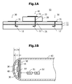
- FIG. 1A is a cross-sectional view of the antenna device according to the first embodiment
- FIG. 1B is a cross-sectional view of a part of the communication device according to the first embodiment
- FIG. 2A is a perspective view of a simulation model having the structure of the antenna device according to the first embodiment
- FIG. 2B is a perspective view of the simulation model according to a comparative example.
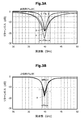
- 3A and 3B are graphs showing the frequency characteristics of the return loss when the second feeding element of the simulation model shown in FIGS. 2A and 2B is fed, respectively.
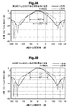
- 4A and 4B are graphs showing directional characteristics when a high frequency signal of 40 GHz is supplied to the second feeding element of the simulation model shown in FIGS. 2A and 2B, respectively.
- FIGS. 5A and 5B are graphs showing directional characteristics when a high frequency signal of 40 GHz is supplied to the first power feeding element on the positive side of the y-axis of the simulation model shown in FIGS. 2A and 2B, respectively.
- FIG. 6A is a cross-sectional view of the antenna device according to a modified example of the first embodiment
- FIG. 6B is a cross-sectional view of the antenna device according to another modified example of the first embodiment
- FIG. 6C is a sectional view of the antenna device according to the first embodiment. It is a perspective view of the antenna device by still another modification of.
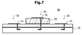
- FIG. 7 is a cross-sectional view of the antenna device according to the second embodiment.
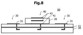
- FIG. 8 is a cross-sectional view of the antenna device according to the third embodiment.
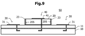
- FIG. 9 is a cross-sectional view of the antenna device according to the fourth embodiment.
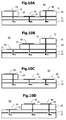
- 10A is a cross-sectional view of the antenna device 50 according to the fifth embodiment
- FIGS. 10B, 10C, and 10D are cross-sectional views of the antenna device according to a modified example of the fifth embodiment, respectively.
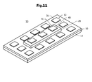
- FIG. 11 is a perspective view of the antenna device according to the sixth embodiment.
- FIG. 12 is a perspective view of the antenna device according to a modified example of the sixth embodiment.
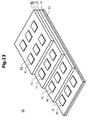
- FIG. 13 is a perspective view of the antenna device according to another modification of the sixth embodiment.
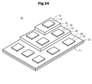
- FIG. 14 is a perspective view of the antenna device according to still another modification of the sixth embodiment.
- FIG. 1A is a cross-sectional view of the antenna device 50 according to the first embodiment.
- the additional member 20 is arranged on one surface (hereinafter, referred to as an upper surface) of the dielectric substrate 10.
- the additional member 20 is fixed to the dielectric substrate 10 with, for example, an adhesive.
- the additional member 20 is made of the same dielectric material as the dielectric substrate 10. In a plan view, the additional member 20 overlaps a part of the upper surface of the dielectric substrate 10. That is, a region on which the additional member 20 is not arranged is secured on the upper surface of the dielectric substrate 10.
- the additional member 20 has an upper surface parallel to the upper surface of the dielectric substrate 10.
- a pair of first antenna elements 30 are arranged on the dielectric substrate 10 so as to sandwich the additional member 20 in a plan view.
- Each of the first antenna elements 30 is composed of a first feeding element 31 made of a metal film arranged on the upper surface of the dielectric substrate 10.
- the second antenna element 40 is arranged on the additional member 20.
- the second antenna element 40 is composed of a second feeding element 41 made of a metal film arranged on the upper surface of the additional member 20.
- the ground plane 11 is arranged on the inner layer of the dielectric substrate 10. Further, a plurality of power feeding lines 12 are arranged in the dielectric substrate 10.
- the feeding line 12 includes a microstrip line or a strip line having a triplate structure, and a via conductor extending in the thickness direction of the dielectric substrate 10.
- the two first power feeding elements 31 are connected to the power feeding line 12, respectively. A high frequency signal is supplied to the first feeding element 31 via the feeding line 12.
- Each of the two first feeding elements 31 and the ground plane 11 operate as a patch antenna.
- a feeding line 22 made of a via conductor connected to the second feeding element 41 is arranged in the additional member 20.
- the power supply line 22 is connected to the power supply line 12 arranged on the dielectric substrate 10 via solder 21.
- a high frequency signal is supplied to the second feeding element 41 via the feeding line 12, the solder 21, and the feeding line 22.
- the second feeding element 41 and the ground plane 11 operate as a patch antenna.
- the two first antenna elements 30 are directly supported by the dielectric substrate 10, and the second antenna element 40 is supported by the dielectric substrate 10 via the additional member 20.
- the first antenna element 30 and the second antenna element 40 are arranged on the same side (upper surface side of the dielectric substrate 10) as viewed from the ground plane 11.
- the ground plane 11 as a reference for height
- the top of the second antenna element 40 is arranged at a position higher than the top of the first antenna element 30. That is, the second feeding element 41 is arranged at a position higher than that of the first feeding element 31. Therefore, the distance from the ground plane 11 to the second feeding element 41 is wider than the distance from the ground plane 11 to the first feeding element 31.
- FIG. 1B is a cross-sectional view of a part of the communication device according to the first embodiment.
- the antenna device 50, the high frequency integrated circuit element (RFIC) 51, and the baseband integrated circuit element (BBIC) 52 shown in FIG. 1A are housed in the housing 60.
- a part of the inner surface of the housing 60 includes a pillar surface 61 curved so as to be convex toward the outside of the housing 60.
- the first antenna element 30 and the second antenna element 40 are supported in the housing 60 in a posture in which the first antenna element 30 and the second antenna element 40 face the pillar surface 61 and the ground plane 11 is parallel to the generatrix of the pillar surface 61.
- the antenna device 50 is housed in a posture in which the direction in which the two first antenna elements 30 and the one second antenna element 40 are arranged is orthogonal to the generatrix of the column surface 61. It is supported within the body 60.
- the distance L2 from the ground plane 11 to the pillar surface 61 intersecting the second antenna element 40 is longer than the distance L1 from the ground plane 11 to the pillar surface 61 intersecting the first antenna element 30.
- BBIC52 performs baseband signal processing.
- a baseband signal or an intermediate frequency signal is input from the BBIC 52 to the RFIC 51.
- the RFIC 51 up-converts the baseband signal or the intermediate frequency signal, and supplies the high frequency signal to the first feeding element 31 and the second feeding element 41 via the feeding lines 12, 22 (FIG. 1A) and the like.
- the RFIC 51 further down-converts the high frequency signal received by the first feeding element 31 and the second feeding element 41.
- the down-converted signal is input to the BBIC 52.
- the second feeding element 41 is arranged at a position higher than the upper surface of the dielectric substrate 10 when viewed from the ground plane 11. That is, the distance from the ground plane 11 to the second feeding element 41 is wider than the distance from the ground plane 11 to the upper surface of the dielectric substrate 10. Therefore, the operating band of the second antenna element 40 can be expanded as compared with the configuration in which the second feeding element 41 is arranged at the same height as the first feeding element 31.
- the distance L2 from the ground plane 11 to the pillar surface 61 intersecting with the second antenna element 40 is longer than the distance L1 from the ground plane 11 to intersecting the first antenna element 30 to reach the pillar surface 61. ..
- the second feeding element 41 is arranged on the upper surface of the dielectric substrate 10, it is difficult to use the space between the second antenna element 40 and the pillar surface 61 for other purposes. Since it is difficult to use the space occupied by the additional member 20 and the second antenna element 40 for other purposes, even if the additional member 20 and the second antenna element 40 are arranged in the housing 60, other parts are used. It does not narrow the space for accommodating. In this way, it is possible to increase the bandwidth of the antenna device 50 without occupying an extra space in the housing 60.
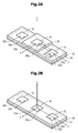
- FIG. 2A is a perspective view of a simulation model having the structure of the antenna device 50 according to the first embodiment
- FIG. 2B is a perspective view of the simulation model according to a comparative example.
- Each component of the simulation model shown in FIG. 2A is assigned the same reference code as the reference code attached to the corresponding component of the antenna device 50 (FIG. 1A) according to the first embodiment.
- each of the first feeding element 31 and the second feeding element 41 in a plan view is square.
- the centers of one first feeding element 31, the second feeding element 41, and the other first feeding element 31 are located on one straight line in this order in a plan view.
- An xyz Cartesian coordinate system is defined in which the direction of this straight line is the y-axis direction and the normal direction of the upper surface of the dielectric substrate 10 is the z-axis direction.
- the edges of the first feeding element 31 and the second feeding element 41 are parallel to the x-axis direction or the y-axis direction.
- the length L of each side of the first feeding element 31 and the second feeding element 41 was set to 1.9 mm, and the distance G between the first feeding element 31 and the second feeding element 41 in the y-axis direction was set to 5 mm.
- the distance from the ground plane 11 to the first feeding element 31 was 0.172 mm, and the distance from the ground plane 11 to the second feeding element 41 was 0.39 mm.
- Feeding points 32y and 42y are arranged slightly inward from the midpoint of the positive side edge of the y-axis of the first feeding element 31 and the second feeding element 41, respectively, and inside the positive side edge of the x-axis. Feeding points 32x and 42x are arranged slightly inside from the points, respectively.
- the additional member 20 is not arranged, and the distance from the ground plane 11 to the second power feeding element 41 is the same as the distance from the ground plane 11 to the first feeding element 31.
- 3A and 3B are graphs showing the frequency characteristics of the return loss when the second feeding element 41 of the simulation model shown in FIGS. 2A and 2B is fed, respectively.
- the horizontal axis represents the frequency in the unit "GHz”
- the vertical axis represents the return loss in the unit "dB”.
- the curves a and b shown in FIGS. 3A and 3B show the return loss when the feeding points 42x and 42y of the second feeding element 41 are fed, respectively.
- the return losses when power is supplied to the power supply points 32x and 32y of the two first power supply elements 31 substantially overlap as shown by the curve c.
- the operating frequency bandwidths when power is supplied to the feeding points 42x and 42y of the second feeding element 41 are described as FBx and FBy, respectively.
- the operating frequency bandwidths FBx and FBy of the simulation model according to the first embodiment are wider than the operating frequency bandwidths FBx and FBy of the simulation model according to the comparative example, respectively. From this simulation result, it was confirmed that it is possible to widen the bandwidth by adopting the structure according to the first embodiment.
- the first feeding element 31 and the second feeding element 41 are individually fed, but the two first feeding elements 31 and the second feeding element 41 are fed at the same time to operate as an array antenna. Even in the case of making it possible, it is possible to increase the bandwidth by adopting the configuration according to the first embodiment.
- FIGS. 4A and 4B are graphs showing directional characteristics when a high frequency signal of 40 GHz is supplied to the second feeding element 41 of the simulation model shown in FIGS. 2A and 2B, respectively.
- the horizontal axis represents the inclination angle from the z-axis in the unit "degree”
- the vertical axis represents the relative antenna gain with the maximum gain as 0 dB in the unit "dB (DirTotal / Max)”.
- the solid line and the broken line in the graphs of FIGS. 4A and 4B indicate the directional characteristics in the xz plane and the yz plane, respectively.
- the 3 dB beam widths in the x direction and the y direction are about 83 ° and about 101 °, respectively.
- the 3 dB beam widths in the x direction and the y direction are about 82 ° and about 93 °, respectively.
- 5A and 5B are graphs showing directional characteristics when a high frequency signal of 40 GHz is supplied to the first power feeding element 31 on the positive side of the y-axis of the simulation model shown in FIGS. 2A and 2B, respectively.
- the horizontal axis represents the inclination angle from the z-axis in the unit "degree”
- the vertical axis represents the relative antenna gain with the maximum gain as 0 dB in the unit "dB (DirTotal / Max)”.
- the solid line and the broken line in the graphs of FIGS. 5A and 5B indicate the directional characteristics in the xz plane and the yz plane, respectively.
- the 3 dB beam widths in the x direction and the y direction are about 92 ° and about 135 °, respectively.
- the 3 dB beam widths in the x direction and the y direction are about 79 ° and about 78 °, respectively.
- the coverage area was expanded by adopting the configuration of the antenna device 50 according to the first embodiment.
- the directional characteristics when one of the two first feeding elements 31 and one second feeding element 41 is fed is shown, but the two first feeding elements 31 and one second feeding element are shown.
- the coverage area can be expanded even when the power feeding element 41 is simultaneously fed to operate as an array antenna.
- the RFIC 51 (FIG. 1B) is housed in the housing 60, but no specific storage place is mentioned.
- the RFIC 51 may be mounted on the back surface of the dielectric substrate 10 (FIG. 1B).
- the back surface means a surface opposite to the side on which the first antenna element 30 and the second antenna element 40 are supported when viewed from the ground plane 11.
- the RFIC 51 is connected to a feeding line 12 (FIG. 1A) arranged in the inner layer of the dielectric substrate 10. It is preferable to mount a connector on the back surface of the dielectric substrate 10 and connect this connector and the BBIC 52 with a coaxial cable.
- FIG. 6A is a cross-sectional view of the antenna device 50 according to a modified example of the first embodiment.
- one second antenna element 40 (FIG. 1A) is arranged, but in this modified example, two second antenna elements 40 are arranged.
- the two second antenna elements 40 are supported by a common additional member 20.
- the two first antenna elements 30 and the two second antenna elements 40 are arranged on one straight line in a plan view.
- FIG. 6B is a cross-sectional view of the antenna device 50 according to another modification of the first embodiment.
- another additional member 70 is arranged on the additional member 20.
- the third antenna element 71 is supported by the additional member 70.
- the third antenna element 71 includes a third feeding element 72 arranged on the upper surface of the additional member 70.
- the antenna device 50 has a three-stage configuration.
- the antenna device 50 may have a stepped structure of four or more steps.
- FIG. 6C is a perspective view of the antenna device 50 according to still another modification of the first embodiment.
- the two first antenna elements 30 and the one second antenna element 40 are arranged on one straight line in a plan view.
- the plurality of first antenna elements 30 and the plurality of second antenna elements 40 are arranged in a two-dimensional shape, for example, in a matrix.
- a plurality of second antenna elements 40 form a row, and a plurality of rows of first antenna elements 30 are arranged on both sides of the row.
- the second feeding element 41 is arranged at a position higher than the first feeding element 31 with respect to the ground plane 11.
- the third feeding element 72 is further arranged at a position higher than that of the second feeding element 41. Therefore, even in these modified examples, it is possible to increase the bandwidth as in the case of the first embodiment.
- Which of the modified examples is used for the antenna device may be selected according to the required antenna characteristics and the shape of the inner surface of the housing to be accommodated.
- the surface of the housing 60 facing the antenna device 50 is the pillar surface 61 (FIG. 1B), but the inner surface of the housing 60 may be a surface other than the pillar surface. For example, it may be a curved surface curved outward or a stepped surface along these curved surfaces.
- FIG. 7 is a cross-sectional view of the antenna device 50 according to the second embodiment.
- the additional member 20 and the dielectric substrate 10 are formed of the same dielectric material.
- the additional member 20 and the dielectric substrate 10 are made of materials having different dielectric constants from each other.
- the dielectric constant of the additional member 20 is lower than the dielectric constant of the dielectric substrate 10.
- the additional member 20 and the dielectric substrate 10 are made of glass epoxy resin, and the glass content of the additional member 20 is smaller than the glass content of the dielectric substrate 10.
- the excellent effect of the second embodiment will be described.
- the dielectric constant of the additional member 20 becomes low, the wavelength shortening effect becomes small, and the dimension of the second feeding element 41 becomes large under the same condition of the resonance frequency.
- the antenna gain becomes high.
- the Q of the resonator decreases, and as a result, the effect of widening the operating frequency band can be obtained.
- FIG. 8 is a cross-sectional view of the antenna device 50 according to the third embodiment.
- the first antenna element 30 is composed of the second feeding element 41 arranged on the upper surface of the additional member 20.
- the second antenna element 40 includes the second feeding element 41 and at least one non-feeding element 43.
- the second power feeding element 41 is arranged on the upper surface of the dielectric substrate 10.
- the non-feeding element 43 is arranged on the upper surface or the inner layer of the additional member 20.
- the non-feeding element 43 is electromagnetically coupled to the second feeding element 41, and the second feeding element 41, the non-feeding element 43, and the ground plane 11 operate as a stack type patch antenna.
- the first feeding element 31 and the second feeding element 41 are arranged at the same position in the height direction with the ground plane 11 as a reference for the height.
- the top of the second antenna element 40 that is, the upper surface of the non-feeding element 43 arranged on the upper surface of the additional member 20, is arranged at a position higher than the top of the first antenna element 30. Has been done.
- the excellent effect of the third embodiment will be described.
- the non-feeding element 43 is loaded on the second feeding element 41, a wide band can be achieved. Furthermore, the coverage area can be expanded.
- FIG. 9 is a cross-sectional view of the antenna device 50 according to the fourth embodiment.
- a stepped surface 20S formed by a side surface of the additional member 20 is arranged between the first antenna element 30 and the second antenna element 40.
- the region where the second antenna element 40 is arranged is higher than the region where the first antenna element 30 is arranged with the stepped surface 20S as a boundary.
- a reflective member 23 made of metal, for example, copper is attached to the stepped surface 20S.
- the fourth embodiment metal is used for the reflective member 23, but the reflective member 23 may be formed of another material that reflects radio waves in the operating frequency band of the antenna device 50.
- FIG. 10A is a cross-sectional view of the antenna device 50 according to the fifth embodiment.
- the additional member 20 is arranged at the center of the upper surface of the dielectric substrate 10.
- the two additional members 20 are arranged near both ends of the upper surface of the dielectric substrate 10.
- the first feeding element 31 constituting the first antenna element 30 is arranged in the region between the two additional members 20 on the upper surface of the dielectric substrate 10.
- a second feeding element 41 constituting the second antenna element 40 is arranged on each of the two additional members 20.
- the second feeding element 41 is arranged at a position higher than the upper surface of the dielectric substrate 10 when the ground plane 11 is used as a height reference. Therefore, the operating band can be expanded as compared with the case where all the feeding elements are arranged on the upper surface of the dielectric substrate 10.
- the antenna device is arranged so that the first feeding element 31 faces the convex portion, so that the second feeding power is supplied to the region around the convex portion on the inner surface of the housing.
- the element 41 can be brought closer. As a result, the space inside the housing can be effectively used.
- the antenna device according to the modified example of the fifth embodiment will be described with reference to FIGS. 10B, 10C, and 10D.
- the height distribution of the plurality of feeding elements is the arrangement direction of the feeding elements. Symmetrical with respect to the center of.
- the height distribution of the plurality of feeding elements is asymmetric.
- 10B, 10C, and 10D are cross-sectional views of an antenna device according to a modified example of the fifth embodiment, respectively.
- the first layer additional member 20 is arranged in a part of the upper surface of the dielectric substrate 10, and the second layer is added to a part of the upper surface of the additional member 20.
- the member 70 is arranged.
- the additional members 20 and 70 are unevenly arranged on one side (right side in FIG. 10B) of the upper surface of the dielectric substrate 10.
- the dielectric substrate 10 and the two additional members 20 and 70 form a three-step stepped upper surface (corresponding to the tread surface of the staircase).
- the first feeding element 31 constituting the first antenna element 30, the second feeding element 41 constituting the second antenna element 40, and the third feeding element 71 constituting the third antenna element 71 are respectively on the three upper surfaces having different heights.
- the power feeding element 72 is arranged. In a plan view, the first feeding element 31, the second feeding element 41, and the third feeding element 72 are arranged in a row. In this modification, the direction of the main beam is tilted with respect to the normal direction of the upper surface of the dielectric substrate 10 due to the influence of the wall surface made of the dielectric material existing on one side of the first feeding element 31 and the second feeding element 41. be able to.
- a plurality of first feeding elements 31 and one second feeding element 41 are arranged in a row in a plan view, and the second feeding element 41 is arranged at the end of the row.
- the second feeding element 41 at the end of the plurality of feeding elements arranged in a row is arranged at a higher position than the other first feeding elements 31 with the ground plane 11 as a reference for height.
- the direction of the main beam of the central first feeding element 31 is directed with respect to the upper surface of the dielectric substrate 10 due to the influence of the wall surface made of the dielectric material existing on one side of the central first feeding element 31. Tilt.
- the directions of the main beams of the other first feeding element 31 and the second feeding element 41 are substantially perpendicular to the upper surface of the dielectric substrate 10. Therefore, the effect that the directivity of the antenna device 50 is widened can be obtained.
- a plurality of second feeding elements 41 and one first feeding element 31 are arranged in a row in a plan view, and the first feeding element 31 is arranged at the end of the row. There is. That is, the first feeding element 31 at the end is arranged at a position lower than the other second feeding elements 41 among the plurality of feeding elements arranged in a row with the ground plane 11 as a reference for height.
- the effect that the directivity of the antenna device 50 is widened can be obtained as in the modified example shown in FIG. 10C.
- the inner surface of the side surface portion of the housing 60 is curved toward the outside, and the shape of the inner surface is substantially symmetrical in the thickness direction of the internal space of the housing 60.
- the interior space is asymmetrically curved with respect to the thickness direction
- An antenna device having an asymmetrical height distribution of the feeding elements may be used. Which of the modified antenna devices to use may be selected according to the shape of the inner surface of the housing. In the antenna device according to these modifications, the operating band can be expanded as in the fifth embodiment.
- FIG. 11 is a perspective view of the antenna device 50 according to the sixth embodiment
- FIGS. 12, 13, and 14 are perspective views of the antenna device 50 according to a modified example of the sixth embodiment, respectively.
- a plurality of feeding elements are arranged two-dimensionally.
- the additional member 20 is arranged in the inner inner part away from the edge of the upper surface of the dielectric substrate 10.
- a plurality of (for example, three) second feeding elements 41 are arranged on the upper surface of the additional member 20.
- a plurality of (for example, 12) first power feeding elements 31 are arranged so as to surround the additional member 20 in a plan view in a region inside the edge of the dielectric substrate 10 and outside the edge of the additional member 20. There is. That is, in a plan view, the power feeding element in the inner inner part is arranged at a higher position than the power feeding element in the peripheral region on the upper surface of the dielectric substrate 10.
- an annular additional member 20 is arranged along the edge of the upper surface of the dielectric substrate 10.
- the additional member 20 is not arranged in the inner inner part of the upper surface of the dielectric substrate 10.
- a plurality of second feeding elements 41 are arranged on the upper surface of the additional member 20.
- a plurality of first power feeding elements 31 are arranged in a region surrounded by an annular additional member 20 on the upper surface of the dielectric substrate 10. That is, in a plan view, the power feeding element in the peripheral region is arranged at a higher position than the power feeding element in the inner inner part of the upper surface of the dielectric substrate 10.
- the first layer additional member 20 is arranged in a part of the upper surface of the rectangular dielectric substrate 10 in a plan view, and a part of the upper surface of the additional member 20.
- the second layer of the additional member 70 is arranged in the region of the above, and the third layer of the additional member 80 is arranged in a part of the upper surface of the additional member 70.
- the edges of the additional members 20, 70, and 80 are substantially aligned with one edge of the dielectric substrate 10, and a stepped upper surface is formed that descends from this edge toward the opposite edge. ..
- a plurality of third feeding elements 72 and a plurality of fourth feeding elements 82 are arranged.
- the first antenna element 30, the second antenna element 40, the third antenna element 71, and the fourth antenna element are provided by the first feeding element 31, the second feeding element 41, the third feeding element 72, and the fourth feeding element 82, respectively.
- 81 is configured.
- the ground plane 11 is used as a reference for height, the height of the feeding element increases in one direction parallel to one edge of the dielectric substrate 10 in a plan view.
- one vertex of the rectangular dielectric substrate 10, the first layer additional member 20 and the second layer additional member 70 substantially coincide with each other in a plan view.
- a plurality of first power feeding elements 31 are arranged in an L-shaped region (corresponding to a tread surface of a staircase) in which the first layer additional member 20 is not arranged on the upper surface of the dielectric substrate 10.
- a plurality of second feeding elements 41 are arranged in an L-shaped region on the upper surface of the additional member 20 where the second layer additional member 70 is not arranged.
- the third power feeding element 72 is arranged on the upper surface of the additional member 70 of the second layer.
- a plurality of feeding elements having different heights from the ground plane 11 are arranged two-dimensionally.
- the shape of the regions having different heights according to the uneven shape of the inner surface of the housing it is possible to flexibly correspond to various housings. Further, it is also possible to obtain the effect that the directivity of the antenna device 50 changes according to the mode of the two-dimensional distribution of the plurality of feeding elements having different heights.
- a plurality of power feeding elements 31 and 41 are arranged in a matrix of 3 rows and 5 columns in a plan view, but other rows and columns. It may be arranged in a matrix of numbers. For example, it may be arranged in a matrix such as 3 rows and 3 columns and 3 rows and 4 columns.
- the plurality of feeding elements 31, 41, 72, 82 are arranged in a matrix of 3 rows and 5 columns.
- Others may be arranged in a matrix of the number of rows and the number of columns. For example, it may be arranged in a matrix such as 3 rows and 3 columns and 3 rows and 4 columns.
- a plurality of feeding elements 31, 41, 72 are arranged in a matrix of 3 rows and 3 columns in a plan view, but are arranged in a matrix having other numbers of rows and columns. You may. For example, it may be arranged in a matrix of 2 rows and 3 columns, 2 rows and 4 columns, and the like.
- Dielectric substrate 11 Ground plane 12 Feeding line 20 Additional member 20S Step surface 21 Feeding line 22 Solder 23 Reflecting member 30 First antenna element 31 First feeding conductor 32x, 32y Feeding point 40 Second antenna element 41 Second feeding element 42x , 42y Feeding point 43 Non-feeding element 50 Antenna device 51 High frequency integrated circuit element (RFIC) 52 Baseband integrated circuit element (BBIC) 60 Housing 61 Pillar surface 70 Additional member 71 Third antenna element 72 Third feeding element 80 Additional member 81 Fourth antenna element 82 Fourth feeding element
Landscapes
- Engineering & Computer Science (AREA)
- Computer Networks & Wireless Communication (AREA)
- Details Of Aerials (AREA)
- Variable-Direction Aerials And Aerial Arrays (AREA)
- Waveguide Aerials (AREA)
- Support Of Aerials (AREA)
Priority Applications (3)
| Application Number | Priority Date | Filing Date | Title |
|---|---|---|---|
| JP2021573975A JP7283584B2 (ja) | 2020-01-30 | 2021-01-21 | アンテナ装置及び通信装置 |
| CN202180011590.6A CN115053404A (zh) | 2020-01-30 | 2021-01-21 | 天线装置以及通信装置 |
| US17/875,425 US12261368B2 (en) | 2020-01-30 | 2022-07-28 | Antenna device and communication device |
Applications Claiming Priority (2)
| Application Number | Priority Date | Filing Date | Title |
|---|---|---|---|
| JP2020014028 | 2020-01-30 | ||
| JP2020-014028 | 2020-07-09 |
Related Child Applications (1)
| Application Number | Title | Priority Date | Filing Date |
|---|---|---|---|
| US17/875,425 Continuation US12261368B2 (en) | 2020-01-30 | 2022-07-28 | Antenna device and communication device |
Publications (1)
| Publication Number | Publication Date |
|---|---|
| WO2021153418A1 true WO2021153418A1 (ja) | 2021-08-05 |
Family
ID=77079895
Family Applications (1)
| Application Number | Title | Priority Date | Filing Date |
|---|---|---|---|
| PCT/JP2021/002074 Ceased WO2021153418A1 (ja) | 2020-01-30 | 2021-01-21 | アンテナ装置及び通信装置 |
Country Status (4)
| Country | Link |
|---|---|
| US (1) | US12261368B2 (enExample) |
| JP (1) | JP7283584B2 (enExample) |
| CN (1) | CN115053404A (enExample) |
| WO (1) | WO2021153418A1 (enExample) |
Cited By (1)
| Publication number | Priority date | Publication date | Assignee | Title |
|---|---|---|---|---|
| CN114566804A (zh) * | 2022-03-17 | 2022-05-31 | 广东分数维无线科技有限公司 | 一种宽频带毫米波电调寄生天线 |
Families Citing this family (1)
| Publication number | Priority date | Publication date | Assignee | Title |
|---|---|---|---|---|
| KR102239249B1 (ko) * | 2020-02-03 | 2021-04-12 | 주식회사 아모텍 | 콤보 안테나 모듈 및 이의 제조 방법 |
Citations (4)
| Publication number | Priority date | Publication date | Assignee | Title |
|---|---|---|---|---|
| JPH066130A (ja) * | 1992-01-27 | 1994-01-14 | Nippon Telegr & Teleph Corp <Ntt> | アンテナ装置 |
| JP2013219533A (ja) * | 2012-04-09 | 2013-10-24 | Nippon Hoso Kyokai <Nhk> | アンテナ装置 |
| JP2015216520A (ja) * | 2014-05-12 | 2015-12-03 | パナソニックIpマネジメント株式会社 | アンテナ装置 |
| JP2018033078A (ja) * | 2016-08-26 | 2018-03-01 | 株式会社村田製作所 | アンテナモジュール |
Family Cites Families (9)
| Publication number | Priority date | Publication date | Assignee | Title |
|---|---|---|---|---|
| JP2004208040A (ja) * | 2002-12-25 | 2004-07-22 | Matsushita Electric Ind Co Ltd | アンテナ装置 |
| EP1936741A1 (en) | 2006-12-22 | 2008-06-25 | Sony Deutschland GmbH | Flexible substrate integrated waveguides |
| JP6256170B2 (ja) * | 2014-04-18 | 2018-01-10 | 株式会社豊田中央研究所 | 吸着式ヒートポンプシステム及び冷熱生成方法 |
| CN105914458B (zh) * | 2016-06-07 | 2018-11-20 | 武汉芯泰科技有限公司 | 一种可调多频天线 |
| JP6881073B2 (ja) * | 2017-06-22 | 2021-06-02 | Tdk株式会社 | デュアルバンドパッチアンテナ |
| US10263332B2 (en) * | 2017-09-18 | 2019-04-16 | Apple Inc. | Antenna arrays with etched substrates |
| JP7077587B2 (ja) * | 2017-11-17 | 2022-05-31 | Tdk株式会社 | デュアルバンドパッチアンテナ |
| US10784593B1 (en) * | 2018-08-02 | 2020-09-22 | United States Of America As Represented By The Administrator Of The National Aeronautics And Space Administration | Dual-band and wideband patch antenna |
| US12293980B2 (en) * | 2019-09-20 | 2025-05-06 | Qualcomm Incorporated | Package comprising discrete antenna device |
-
2021
- 2021-01-21 JP JP2021573975A patent/JP7283584B2/ja active Active
- 2021-01-21 CN CN202180011590.6A patent/CN115053404A/zh active Pending
- 2021-01-21 WO PCT/JP2021/002074 patent/WO2021153418A1/ja not_active Ceased
-
2022
- 2022-07-28 US US17/875,425 patent/US12261368B2/en active Active
Patent Citations (4)
| Publication number | Priority date | Publication date | Assignee | Title |
|---|---|---|---|---|
| JPH066130A (ja) * | 1992-01-27 | 1994-01-14 | Nippon Telegr & Teleph Corp <Ntt> | アンテナ装置 |
| JP2013219533A (ja) * | 2012-04-09 | 2013-10-24 | Nippon Hoso Kyokai <Nhk> | アンテナ装置 |
| JP2015216520A (ja) * | 2014-05-12 | 2015-12-03 | パナソニックIpマネジメント株式会社 | アンテナ装置 |
| JP2018033078A (ja) * | 2016-08-26 | 2018-03-01 | 株式会社村田製作所 | アンテナモジュール |
Cited By (1)
| Publication number | Priority date | Publication date | Assignee | Title |
|---|---|---|---|---|
| CN114566804A (zh) * | 2022-03-17 | 2022-05-31 | 广东分数维无线科技有限公司 | 一种宽频带毫米波电调寄生天线 |
Also Published As
| Publication number | Publication date |
|---|---|
| CN115053404A (zh) | 2022-09-13 |
| US20220368030A1 (en) | 2022-11-17 |
| US12261368B2 (en) | 2025-03-25 |
| JP7283584B2 (ja) | 2023-05-30 |
| JPWO2021153418A1 (enExample) | 2021-08-05 |
Similar Documents
| Publication | Publication Date | Title |
|---|---|---|
| US12218401B2 (en) | Dielectric covers for antennas | |
| KR102599495B1 (ko) | 안테나 모듈, 및 그것을 탑재한 통신 장치, 그리고 안테나 모듈의 제조 방법 | |
| US10978797B2 (en) | Electronic devices having antenna array apertures mounted against a dielectric layer | |
| KR102639417B1 (ko) | 안테나를 포함하는 전자 장치 | |
| US20210265745A1 (en) | Electronic Device Antenna Arrays Mounted Against a Dielectric Layer | |
| CN108539439B (zh) | 天线装置 | |
| US12413263B2 (en) | Dielectric resonator antenna modules | |
| JP5712964B2 (ja) | アンテナ装置 | |
| CN110785893A (zh) | 天线模块和通信装置 | |
| CN111180906A (zh) | 多频带天线阵列及其无线设备 | |
| US20240145926A1 (en) | Antenna device and communication module | |
| KR101901101B1 (ko) | 인쇄형 다이폴 안테나 및 이를 이용한 전자기기 | |
| US20220368030A1 (en) | Antenna device and communication device | |
| US12381327B2 (en) | Antenna module and communication device including the same | |
| US20250015500A1 (en) | Antenna module and communication apparatus including the same | |
| US20240178567A1 (en) | Antenna module and communication apparatus equipped with the same | |
| JP7660721B2 (ja) | アンテナおよび通信モジュール | |
| US11183752B2 (en) | Antenna structure and antenna array | |
| JP7698717B2 (ja) | アンテナ装置及び無線通信装置 | |
| US20240195079A1 (en) | Antenna device, antenna module, and communication device | |
| JP7608660B2 (ja) | アンテナ装置 | |
| JP7115780B1 (ja) | アレーアンテナ | |
| JP7514682B2 (ja) | アレイアンテナ | |
| KR102389174B1 (ko) | 반구형 방사 패턴을 가지는 밀리미터 웨이브 배열 안테나 | |
| US20250141112A1 (en) | Antenna element and array antenna |
Legal Events
| Date | Code | Title | Description |
|---|---|---|---|
| 121 | Ep: the epo has been informed by wipo that ep was designated in this application |
Ref document number: 21747816 Country of ref document: EP Kind code of ref document: A1 |
|
| ENP | Entry into the national phase |
Ref document number: 2021573975 Country of ref document: JP Kind code of ref document: A |
|
| NENP | Non-entry into the national phase |
Ref country code: DE |
|
| 122 | Ep: pct application non-entry in european phase |
Ref document number: 21747816 Country of ref document: EP Kind code of ref document: A1 |