WO2021153082A1 - 電子機器 - Google Patents
電子機器 Download PDFInfo
- Publication number
- WO2021153082A1 WO2021153082A1 PCT/JP2020/047428 JP2020047428W WO2021153082A1 WO 2021153082 A1 WO2021153082 A1 WO 2021153082A1 JP 2020047428 W JP2020047428 W JP 2020047428W WO 2021153082 A1 WO2021153082 A1 WO 2021153082A1
- Authority
- WO
- WIPO (PCT)
- Prior art keywords
- pixel
- organic
- light
- electronic device
- transistors
- Prior art date
- Legal status (The legal status is an assumption and is not a legal conclusion. Google has not performed a legal analysis and makes no representation as to the accuracy of the status listed.)
- Ceased
Links
Images


Classifications
-
- G—PHYSICS
- G06—COMPUTING OR CALCULATING; COUNTING
- G06V—IMAGE OR VIDEO RECOGNITION OR UNDERSTANDING
- G06V10/00—Arrangements for image or video recognition or understanding
- G06V10/10—Image acquisition
- G06V10/12—Details of acquisition arrangements; Constructional details thereof
-
- G—PHYSICS
- G02—OPTICS
- G02F—OPTICAL DEVICES OR ARRANGEMENTS FOR THE CONTROL OF LIGHT BY MODIFICATION OF THE OPTICAL PROPERTIES OF THE MEDIA OF THE ELEMENTS INVOLVED THEREIN; NON-LINEAR OPTICS; FREQUENCY-CHANGING OF LIGHT; OPTICAL LOGIC ELEMENTS; OPTICAL ANALOGUE/DIGITAL CONVERTERS
- G02F1/00—Devices or arrangements for the control of the intensity, colour, phase, polarisation or direction of light arriving from an independent light source, e.g. switching, gating or modulating; Non-linear optics
- G02F1/01—Devices or arrangements for the control of the intensity, colour, phase, polarisation or direction of light arriving from an independent light source, e.g. switching, gating or modulating; Non-linear optics for the control of the intensity, phase, polarisation or colour
- G02F1/13—Devices or arrangements for the control of the intensity, colour, phase, polarisation or direction of light arriving from an independent light source, e.g. switching, gating or modulating; Non-linear optics for the control of the intensity, phase, polarisation or colour based on liquid crystals, e.g. single liquid crystal display cells
- G02F1/133—Constructional arrangements; Operation of liquid crystal cells; Circuit arrangements
- G02F1/1333—Constructional arrangements; Manufacturing methods
- G02F1/133345—Insulating layers
-
- G—PHYSICS
- G02—OPTICS
- G02F—OPTICAL DEVICES OR ARRANGEMENTS FOR THE CONTROL OF LIGHT BY MODIFICATION OF THE OPTICAL PROPERTIES OF THE MEDIA OF THE ELEMENTS INVOLVED THEREIN; NON-LINEAR OPTICS; FREQUENCY-CHANGING OF LIGHT; OPTICAL LOGIC ELEMENTS; OPTICAL ANALOGUE/DIGITAL CONVERTERS
- G02F1/00—Devices or arrangements for the control of the intensity, colour, phase, polarisation or direction of light arriving from an independent light source, e.g. switching, gating or modulating; Non-linear optics
- G02F1/01—Devices or arrangements for the control of the intensity, colour, phase, polarisation or direction of light arriving from an independent light source, e.g. switching, gating or modulating; Non-linear optics for the control of the intensity, phase, polarisation or colour
- G02F1/13—Devices or arrangements for the control of the intensity, colour, phase, polarisation or direction of light arriving from an independent light source, e.g. switching, gating or modulating; Non-linear optics for the control of the intensity, phase, polarisation or colour based on liquid crystals, e.g. single liquid crystal display cells
- G02F1/133—Constructional arrangements; Operation of liquid crystal cells; Circuit arrangements
- G02F1/1333—Constructional arrangements; Manufacturing methods
- G02F1/1335—Structural association of cells with optical devices, e.g. polarisers or reflectors
- G02F1/133509—Filters, e.g. light shielding masks
- G02F1/133512—Light shielding layers, e.g. black matrix
-
- G—PHYSICS
- G02—OPTICS
- G02F—OPTICAL DEVICES OR ARRANGEMENTS FOR THE CONTROL OF LIGHT BY MODIFICATION OF THE OPTICAL PROPERTIES OF THE MEDIA OF THE ELEMENTS INVOLVED THEREIN; NON-LINEAR OPTICS; FREQUENCY-CHANGING OF LIGHT; OPTICAL LOGIC ELEMENTS; OPTICAL ANALOGUE/DIGITAL CONVERTERS
- G02F1/00—Devices or arrangements for the control of the intensity, colour, phase, polarisation or direction of light arriving from an independent light source, e.g. switching, gating or modulating; Non-linear optics
- G02F1/01—Devices or arrangements for the control of the intensity, colour, phase, polarisation or direction of light arriving from an independent light source, e.g. switching, gating or modulating; Non-linear optics for the control of the intensity, phase, polarisation or colour
- G02F1/13—Devices or arrangements for the control of the intensity, colour, phase, polarisation or direction of light arriving from an independent light source, e.g. switching, gating or modulating; Non-linear optics for the control of the intensity, phase, polarisation or colour based on liquid crystals, e.g. single liquid crystal display cells
- G02F1/133—Constructional arrangements; Operation of liquid crystal cells; Circuit arrangements
- G02F1/1333—Constructional arrangements; Manufacturing methods
- G02F1/1335—Structural association of cells with optical devices, e.g. polarisers or reflectors
- G02F1/133509—Filters, e.g. light shielding masks
- G02F1/133514—Colour filters
-
- G—PHYSICS
- G02—OPTICS
- G02F—OPTICAL DEVICES OR ARRANGEMENTS FOR THE CONTROL OF LIGHT BY MODIFICATION OF THE OPTICAL PROPERTIES OF THE MEDIA OF THE ELEMENTS INVOLVED THEREIN; NON-LINEAR OPTICS; FREQUENCY-CHANGING OF LIGHT; OPTICAL LOGIC ELEMENTS; OPTICAL ANALOGUE/DIGITAL CONVERTERS
- G02F1/00—Devices or arrangements for the control of the intensity, colour, phase, polarisation or direction of light arriving from an independent light source, e.g. switching, gating or modulating; Non-linear optics
- G02F1/01—Devices or arrangements for the control of the intensity, colour, phase, polarisation or direction of light arriving from an independent light source, e.g. switching, gating or modulating; Non-linear optics for the control of the intensity, phase, polarisation or colour
- G02F1/13—Devices or arrangements for the control of the intensity, colour, phase, polarisation or direction of light arriving from an independent light source, e.g. switching, gating or modulating; Non-linear optics for the control of the intensity, phase, polarisation or colour based on liquid crystals, e.g. single liquid crystal display cells
- G02F1/133—Constructional arrangements; Operation of liquid crystal cells; Circuit arrangements
- G02F1/136—Liquid crystal cells structurally associated with a semi-conducting layer or substrate, e.g. cells forming part of an integrated circuit
- G02F1/1362—Active matrix addressed cells
- G02F1/136209—Light shielding layers, e.g. black matrix, incorporated in the active matrix substrate, e.g. structurally associated with the switching element
-
- G—PHYSICS
- G02—OPTICS
- G02F—OPTICAL DEVICES OR ARRANGEMENTS FOR THE CONTROL OF LIGHT BY MODIFICATION OF THE OPTICAL PROPERTIES OF THE MEDIA OF THE ELEMENTS INVOLVED THEREIN; NON-LINEAR OPTICS; FREQUENCY-CHANGING OF LIGHT; OPTICAL LOGIC ELEMENTS; OPTICAL ANALOGUE/DIGITAL CONVERTERS
- G02F1/00—Devices or arrangements for the control of the intensity, colour, phase, polarisation or direction of light arriving from an independent light source, e.g. switching, gating or modulating; Non-linear optics
- G02F1/01—Devices or arrangements for the control of the intensity, colour, phase, polarisation or direction of light arriving from an independent light source, e.g. switching, gating or modulating; Non-linear optics for the control of the intensity, phase, polarisation or colour
- G02F1/13—Devices or arrangements for the control of the intensity, colour, phase, polarisation or direction of light arriving from an independent light source, e.g. switching, gating or modulating; Non-linear optics for the control of the intensity, phase, polarisation or colour based on liquid crystals, e.g. single liquid crystal display cells
- G02F1/133—Constructional arrangements; Operation of liquid crystal cells; Circuit arrangements
- G02F1/136—Liquid crystal cells structurally associated with a semi-conducting layer or substrate, e.g. cells forming part of an integrated circuit
- G02F1/1362—Active matrix addressed cells
- G02F1/136286—Wiring, e.g. gate line, drain line
-
- G—PHYSICS
- G02—OPTICS
- G02F—OPTICAL DEVICES OR ARRANGEMENTS FOR THE CONTROL OF LIGHT BY MODIFICATION OF THE OPTICAL PROPERTIES OF THE MEDIA OF THE ELEMENTS INVOLVED THEREIN; NON-LINEAR OPTICS; FREQUENCY-CHANGING OF LIGHT; OPTICAL LOGIC ELEMENTS; OPTICAL ANALOGUE/DIGITAL CONVERTERS
- G02F1/00—Devices or arrangements for the control of the intensity, colour, phase, polarisation or direction of light arriving from an independent light source, e.g. switching, gating or modulating; Non-linear optics
- G02F1/01—Devices or arrangements for the control of the intensity, colour, phase, polarisation or direction of light arriving from an independent light source, e.g. switching, gating or modulating; Non-linear optics for the control of the intensity, phase, polarisation or colour
- G02F1/13—Devices or arrangements for the control of the intensity, colour, phase, polarisation or direction of light arriving from an independent light source, e.g. switching, gating or modulating; Non-linear optics for the control of the intensity, phase, polarisation or colour based on liquid crystals, e.g. single liquid crystal display cells
- G02F1/133—Constructional arrangements; Operation of liquid crystal cells; Circuit arrangements
- G02F1/136—Liquid crystal cells structurally associated with a semi-conducting layer or substrate, e.g. cells forming part of an integrated circuit
- G02F1/1362—Active matrix addressed cells
- G02F1/1368—Active matrix addressed cells in which the switching element is a three-electrode device
-
- G—PHYSICS
- G06—COMPUTING OR CALCULATING; COUNTING
- G06V—IMAGE OR VIDEO RECOGNITION OR UNDERSTANDING
- G06V40/00—Recognition of biometric, human-related or animal-related patterns in image or video data
- G06V40/10—Human or animal bodies, e.g. vehicle occupants or pedestrians; Body parts, e.g. hands
- G06V40/12—Fingerprints or palmprints
- G06V40/13—Sensors therefor
- G06V40/1318—Sensors therefor using electro-optical elements or layers, e.g. electroluminescent sensing
-
- H—ELECTRICITY
- H10—SEMICONDUCTOR DEVICES; ELECTRIC SOLID-STATE DEVICES NOT OTHERWISE PROVIDED FOR
- H10K—ORGANIC ELECTRIC SOLID-STATE DEVICES
- H10K50/00—Organic light-emitting devices
- H10K50/80—Constructional details
- H10K50/86—Arrangements for improving contrast, e.g. preventing reflection of ambient light
- H10K50/865—Arrangements for improving contrast, e.g. preventing reflection of ambient light comprising light absorbing layers, e.g. light-blocking layers
-
- H—ELECTRICITY
- H10—SEMICONDUCTOR DEVICES; ELECTRIC SOLID-STATE DEVICES NOT OTHERWISE PROVIDED FOR
- H10K—ORGANIC ELECTRIC SOLID-STATE DEVICES
- H10K59/00—Integrated devices, or assemblies of multiple devices, comprising at least one organic light-emitting element covered by group H10K50/00
- H10K59/10—OLED displays
- H10K59/12—Active-matrix OLED [AMOLED] displays
- H10K59/131—Interconnections, e.g. wiring lines or terminals
-
- H—ELECTRICITY
- H10—SEMICONDUCTOR DEVICES; ELECTRIC SOLID-STATE DEVICES NOT OTHERWISE PROVIDED FOR
- H10K—ORGANIC ELECTRIC SOLID-STATE DEVICES
- H10K59/00—Integrated devices, or assemblies of multiple devices, comprising at least one organic light-emitting element covered by group H10K50/00
- H10K59/30—Devices specially adapted for multicolour light emission
- H10K59/35—Devices specially adapted for multicolour light emission comprising red-green-blue [RGB] subpixels
- H10K59/352—Devices specially adapted for multicolour light emission comprising red-green-blue [RGB] subpixels the areas of the RGB subpixels being different
-
- H—ELECTRICITY
- H10—SEMICONDUCTOR DEVICES; ELECTRIC SOLID-STATE DEVICES NOT OTHERWISE PROVIDED FOR
- H10K—ORGANIC ELECTRIC SOLID-STATE DEVICES
- H10K59/00—Integrated devices, or assemblies of multiple devices, comprising at least one organic light-emitting element covered by group H10K50/00
- H10K59/60—OLEDs integrated with inorganic light-sensitive elements, e.g. with inorganic solar cells or inorganic photodiodes
- H10K59/65—OLEDs integrated with inorganic image sensors
-
- G—PHYSICS
- G02—OPTICS
- G02F—OPTICAL DEVICES OR ARRANGEMENTS FOR THE CONTROL OF LIGHT BY MODIFICATION OF THE OPTICAL PROPERTIES OF THE MEDIA OF THE ELEMENTS INVOLVED THEREIN; NON-LINEAR OPTICS; FREQUENCY-CHANGING OF LIGHT; OPTICAL LOGIC ELEMENTS; OPTICAL ANALOGUE/DIGITAL CONVERTERS
- G02F2201/00—Constructional arrangements not provided for in groups G02F1/00 - G02F7/00
- G02F2201/52—RGB geometrical arrangements
-
- H—ELECTRICITY
- H10—SEMICONDUCTOR DEVICES; ELECTRIC SOLID-STATE DEVICES NOT OTHERWISE PROVIDED FOR
- H10K—ORGANIC ELECTRIC SOLID-STATE DEVICES
- H10K59/00—Integrated devices, or assemblies of multiple devices, comprising at least one organic light-emitting element covered by group H10K50/00
- H10K59/10—OLED displays
- H10K59/12—Active-matrix OLED [AMOLED] displays
- H10K59/126—Shielding, e.g. light-blocking means over the TFTs
-
- H—ELECTRICITY
- H10—SEMICONDUCTOR DEVICES; ELECTRIC SOLID-STATE DEVICES NOT OTHERWISE PROVIDED FOR
- H10K—ORGANIC ELECTRIC SOLID-STATE DEVICES
- H10K59/00—Integrated devices, or assemblies of multiple devices, comprising at least one organic light-emitting element covered by group H10K50/00
- H10K59/80—Constructional details
- H10K59/8791—Arrangements for improving contrast, e.g. preventing reflection of ambient light
- H10K59/8792—Arrangements for improving contrast, e.g. preventing reflection of ambient light comprising light absorbing layers, e.g. black layers
Definitions
- the embodiment of the present invention relates to an electronic device.
- the present embodiment provides an electronic device capable of capturing a clear image.
- the electronic device includes an image pickup device and a liquid crystal panel having a display unit superimposed on the image pickup device, and the liquid crystal panel includes a first pixel superposed on the image pickup device and the first pixel.
- the third pixel includes at least a first color, a second color, and a second pixel adjacent to the first pixel, and a third pixel adjacent to the second pixel. It has a colored layer of a third color, and the second pixel does not have the colored layer or has a transparent resin layer.
- the electronic device includes an imaging device and an organic EL panel having a display unit superimposed on the imaging device, and the organic EL panel includes a first pixel superimposed on the imaging device.
- An opening provided in the first pixel, a second pixel adjacent to the first pixel, and a third pixel adjacent to the second pixel are provided, and the third pixel is at least the first color. It has a colored layer of a second color and a third color, and the second pixel has a transparent resin layer.
- FIG. 1 is an exploded perspective view showing a configuration example of the electronic device 100 of the first embodiment.
- FIG. 2 is a cross-sectional view of the periphery of the image pickup apparatus 1 of the electronic device 100 shown in FIG.
- FIG. 3 is a plan view showing a configuration example of the liquid crystal panel PNL shown in FIG.
- FIG. 4 is an enlarged plan view of the liquid crystal panel PNL shown in FIG.
- FIG. 5 is an enlarged plan view of the pixel PPX, the pixel BPX, the pixel LPX, and the pixel PX shown in FIG.
- FIG. 6 is a cross-sectional view of the liquid crystal element LCD along the line AB shown in FIG.
- FIG. 7 (A) and 7 (B) are cross-sectional views of the liquid crystal element LCD along the CD line shown in FIG. 5, respectively.
- FIG. 8 is a cross-sectional view of the liquid crystal element LCD along the line EF shown in FIG.
- FIG. 9 is a cross-sectional view of the liquid crystal element LCD along the line GH shown in FIG.
- FIG. 10 is a plan view showing another configuration example of the opening POP.
- FIG. 11 is a plan view showing another configuration example of the sub-pixel LSP.
- FIG. 12 is a cross-sectional view of the pixel LPX.
- FIG. 13 is a diagram showing the relationship of brightness with respect to the applied voltage in the pixel LPX and the pixel PX.
- FIG. 14 is a diagram showing another configuration example of the liquid crystal panel PNL.
- FIG. 15 is a diagram showing another configuration example of the liquid crystal panel PNL.
- FIG. 16 is a diagram showing another configuration example of the pixel LPX.
- FIG. 17 is a plan view showing another configuration example of the pixel layout.
- FIG. 18 is a plan view showing the pixel PPX, the pixel BPX, the pixel LPX, and the sub-pixel SP1 shown in FIG.
- FIG. 19 is a plan view showing another configuration example of the pixel layout in the present embodiment.
- FIG. 20 is a perspective view showing the configuration of the electronic device 100 of the second embodiment.
- FIG. 21 is a plan view showing the circuit configuration of the display panel DSP.
- FIG. 22 is a plan view showing the circuit configuration of the display panel DSP.
- FIG. 21 is a plan view showing the circuit configuration of the display panel DSP.
- FIG. 23 is a schematic view showing a cross section showing the display unit DA of the display panel DSP shown in FIG. 20.
- FIG. 24 is a timing chart showing output examples of various signals related to a reset operation, an offset cancel operation, a writing operation, and a light emitting operation in the organic EL element OLED.
- FIG. 25 is a plan view showing the pixel layout.
- FIG. 26 is another plan view showing the pixel layout.
- FIG. 27 is a cross-sectional view showing another configuration example of the pixel LPX.
- FIG. 28 is a diagram showing a voltage Vsig of another configuration example.
- FIG. 29 is a diagram showing another configuration example of the display panel DSP.
- FIG. 30 is a diagram showing another configuration example of the display panel DSP.
- FIG. 31 is a diagram showing another configuration example of the pixel LPX.
- FIG. 32 is a timing chart showing an output example of the pixel control signal SG applied to the scanning line G (control wiring SSG) of the pixel LPX.
- FIG. 33 is a diagram showing another configuration example of the pixel circuit PC of the present embodiment.
- first direction X, the second direction Y, and the third direction Z are orthogonal to each other, but may intersect at an angle other than 90 degrees.
- the direction toward the tip of the arrow in the third direction Z is defined as up or up, and the direction opposite to the direction toward the tip of the arrow in the third direction Z is defined as down or down.
- the second member in the case of "the second member above the first member” and “the second member below the first member”, the second member may be in contact with the first member or separated from the first member. May be located. In the latter case, a third member may be interposed between the first member and the second member. On the other hand, in the case of “the second member above the first member” and “the second member below the first member”, the second member is in contact with the first member.
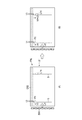
- FIG. 1 is an exploded perspective view showing a configuration example of the electronic device 100 of the present embodiment.
- the electronic device 100 includes a liquid crystal panel PNL, a lighting device IL, and an image pickup device 1.
- the lighting device IL includes a light guide plate LG1, a light source EM1, and a case CS.
- the illuminating device IL illuminates the liquid crystal panel PNL shown simply by the broken line in FIG. 1, for example.
- the light guide plate LG1 is formed in a flat plate shape parallel to the XY plane defined by the first direction X and the second direction Y.
- the light guide plate LG1 faces the liquid crystal panel PNL.
- the light guide plate LG1 has a side surface SA, a side surface SB on the opposite side of the side surface SA, and an opening OP1.
- the side surfaces SA and SB extend along the first direction X, respectively.
- the side surfaces SA and SB are planes parallel to the XX plane defined by the first direction X and the third direction Z.
- the opening OP1 is a through hole that penetrates the light guide plate LG1 along the third direction Z.
- the opening OP1 is located between the side surface SA and the SB in the second direction Y, and is closer to the side surface SB than the side surface SA.
- the opening OP1 may be a recess or a notch recessed from the side surface SB toward the side surface SA.
- the plurality of light sources EM1 are arranged at intervals along the first direction X. Each of the light sources EM1 is mounted on the wiring board F1 and is electrically connected to the wiring board F1.
- the light source EM1 is, for example, a light emitting diode (LED) and emits white illumination light.
- the illumination light emitted from the light source EM1 enters the light guide plate LG1 from the side surface SA and travels from the side surface SA toward the side surface SB.
- the case CS houses the light guide plate LG1 and the light source EM1.
- the case CS has side walls W1 to W4, a bottom plate BP, an opening OP2, and a protrusion PP.
- the side walls W1 and W2 extend along the first direction X and face each other.
- the side walls W3 and W4 extend along the second direction Y and face each other.
- the opening OP2 is superimposed on the opening OP1 in the third direction Z.
- the protrusion PP projects from the bottom plate BP toward the liquid crystal panel PNL along the third direction Z, and is provided so as to surround the opening OP2.
- the image pickup apparatus 1 is provided so as to overlap the opening OP2 in the third direction Z.
- the image pickup apparatus 1 is mounted on the wiring board F2 and is electrically connected to the wiring board F2.
- the liquid crystal panel PNL is superimposed on the light guide plate LG1 and is superimposed on the image pickup apparatus 1 at the opening OP1.
- FIG. 2 is a cross-sectional view of the periphery of the image pickup apparatus 1 of the electronic device 100 shown in FIG.
- the positional relationship between the optical system 2, the color filter CF, the light-shielding layer BMA, and the light-shielding layer BM shown in FIG. 2 is not described here, but details will be described later.
- the lighting device IL further includes a reflective sheet RS, a diffusion sheet SS, and prism sheets PS1 and PS2.
- the reflective sheet RS, the light guide plate LG1, the diffusion sheet SS, the prism sheet PS1, and the prism sheet PS2 are arranged in this order along the third direction Z and are housed in the case CS.
- the case CS includes a metal case CS1 and a resin pedestal CS2.
- the pedestal CS2 forms a protrusion PP together with the case CS1.
- Each of the diffusion sheet SS, the prism sheet PS1, and the prism sheet PS2 has a through hole that overlaps with the opening OP1.
- the reflective sheet RS has a through hole that overlaps with the opening OP1.
- the protrusion PP is located inside the opening OP1.
- the polarizing plate PL1, the liquid crystal panel PNL, the polarizing plate PL2, and the cover glass CG are arranged in this order along the third direction Z, and have an optical switch function for light traveling along the third direction Z. It constitutes a liquid crystal element LCD provided with.
- the adhesive tape TP1 adheres the lighting device IL and the liquid crystal element LCD. In the present embodiment, the adhesive tape TP1 adheres the polarizing plate PL1 and the protrusion PP, and the polarizing plate PL1 and the prism sheet PS2.
- the liquid crystal panel PNL has a display mode that uses a lateral electric field along the main surface of the substrate, a display mode that uses a vertical electric field along the normal line of the main surface of the substrate, and a gradient electric field that is inclined in an oblique direction with respect to the main surface of the substrate. Any configuration corresponding to the display mode to be used and the display mode in which the above-mentioned lateral electric field, longitudinal electric field, and gradient electric field are appropriately combined may be provided.
- the main surface of the substrate here is a surface parallel to the XY plane.
- the liquid crystal panel PNL includes a display unit DA that displays pixels and a non-display unit NDA that surrounds the display unit DA.
- the liquid crystal panel PNL includes a first substrate SUB1, a second substrate SUB2, a liquid crystal layer LC, and a seal SE.
- the seal SE is located in the non-display portion NDA, adheres the first substrate SUB1 and the second substrate SUB2, and seals the liquid crystal layer LC.
- the first substrate SUB1 includes an insulating substrate 10 and an alignment film AL1.
- the second substrate SUB2 includes an insulating substrate 20, a color filter CF, a light-shielding layer BMA, a transparent layer OC, and an alignment film AL2.
- the insulating substrate 10 and the insulating substrate 20 are transparent substrates such as a glass substrate and a flexible resin substrate.
- the alignment films AL1 and AL2 are in contact with the liquid crystal layer LC.
- the color filter CF, the light-shielding layer BMA, and the transparent layer OC are located between the insulating substrate 20 and the liquid crystal layer LC in the third direction Z.
- the color filter CF is provided on the second substrate SUB2, but it may be provided on the first substrate SUB1.
- the color filter CF includes, for example, a red color filter arranged in the red pixel, a green color filter arranged in the green pixel, and blue arranged in the blue pixel. It has a color filter.
- the color filter CF may include a transparent resin layer arranged in white pixels.
- the transparent layer OC covers the color fitter CF and the light-shielding layer BMA.
- the transparent layer OC is, for example, a transparent organic insulating layer.
- the light-shielding layer BMA is located in the non-display part NDA.
- the boundary L between the display unit DA and the non-display unit NDA is defined by, for example, the inner end of the light-shielding layer BMA (the end on the display unit DA side).
- the seal SE is provided at a position where it overlaps with the light-shielding layer BMA.
- the alignment films AL1 and AL2 are provided over the display unit DA and the non-display unit NDA.
- the image pickup device 1 is provided so as to overlap the opening OP2 of the case CS, and is located inside surrounded by the protrusion PP.
- the image pickup apparatus 1 is superimposed on the cover glass CG, the polarizing plate PL2, the liquid crystal panel PNL, and the polarizing plate PL1 in the third direction Z.
- the image pickup apparatus 1 is superimposed on the display unit DA of the liquid crystal panel PNL in the third direction Z. That is, in the electronic device 100 having the liquid crystal panel PNL and the image pickup device 1, the image pickup device 1 may be provided on the back side of the liquid crystal panel PNL from the viewpoint of the user of the electronic device 100.
- the image pickup device 1 includes, for example, an optical system 2 including at least one lens, an image sensor (imaging element) 3, and a case 4.
- the case 4 houses the optical system 2 and the image sensor 3.
- the optical system 2 is located between the liquid crystal panel PNL and the image sensor 3.
- the image sensor 3 receives light through the cover glass CG, the polarizing plate PL2, the liquid crystal panel PNL, and the polarizing plate PL1.
- the image pickup apparatus 1 receives visible light (for example, light in the range of 400 nm to 700 nm) transmitted through the cover glass CG, the polarizing plate PL2, the display unit DA, the polarizing plate PL1, and the light guide plate LG2.
- visible light for example, light in the range of 400 nm to 700 nm
- the retardation of the liquid crystal layer LC is almost zero or ⁇ when the wavelength of the light transmitted through the liquid crystal layer LC of the liquid crystal element LCD is ⁇ . In the case corresponding to, the transmittance of the liquid crystal element LCD is minimized.
- the retardation of the liquid crystal layer LC is set to be larger than zero and smaller than ⁇ .
- the retardation is about ⁇ / 2
- the transmittance of the liquid crystal element LCD is maximized.
- the polarizing plate PL1 is adhered to the insulating substrate 10.
- the polarizing plate PL2 is adhered to the insulating substrate 20.
- the polarizing plate PL2 is adhered to the cover glass CG by the transparent adhesive layer AD.
- the polarizing plates PL1 and PL2 may be provided with a retardation plate, a scattering layer, an antireflection layer, and the like, if necessary.
- a transparent conductive film may be provided between the polarizing plate PL2 and the insulating substrate 20.
- the transparent conductive film is made of a transparent oxide conductor such as indium tin oxide (ITO) or indium zinc oxide (IZO).
- ITO indium tin oxide
- IZO indium zinc oxide
- a transparent conductive film may be formed at a position where the infrared ray transmittance is not a problem and is superimposed on the visible light camera 1.
- polarizing plate PL1 or the polarizing plate PL2 it is also possible to equip the polarizing plate PL1 or the polarizing plate PL2 with a super birefringent film.
- Super birefringent film is known to depolarize (naturalize) transmitted light when linearly polarized light is incident, and it is possible to shoot without discomfort even if the subject contains something that emits polarized light. ..
- the electronic device 100 or the like when the electronic device 100 or the like is reflected on the subject of the image pickup apparatus 1, linearly polarized light is emitted from the electronic device 100, so that the polarizing plate PL1 and the polarizing plate PL2 and the electronic device 100 which is the subject are emitted.
- the brightness of the electronic device 100 of the subject incident on the imaging device 1 changes depending on the angle with the polarizing plate, which may cause a sense of discomfort during shooting.
- the polarizing plate PL1 and the polarizing plate PL2 with a super birefringent film, it is possible to suppress a change in brightness that causes a sense of discomfort.
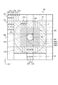
- FIG. 3 is a plan view showing a configuration example of the liquid crystal panel PNL shown in FIG.
- the liquid crystal layer LC and the seal SE are shown by different diagonal lines.
- the outer shape of the optical system 2 of the image pickup apparatus 1 is shown by a broken line.
- the display unit DA is a substantially quadrangular region that does not include a notch, but the four corners may be rounded, or may be a polygon or a circle other than the quadrangle.
- the display unit DA is located inside surrounded by the seal SE.
- the liquid crystal panel PNL has a pair of short sides E11 and E12 extending along the first direction X and a pair of long sides E13 and E14 extending along the second direction Y.
- the liquid crystal panel PNL includes a plurality of pixels PX arranged in a matrix in the first direction X and the second direction Y in the display unit DA. Each pixel PX in the display unit DA has the same circuit configuration.
- each pixel PX includes a switching element SW, a pixel electrode PE, a common electrode CE, a liquid crystal layer LC, and the like.
- the switching element SW is composed of, for example, a transistor, more specifically, a thin film transistor (TFT), and is electrically connected to a scanning line G and a signal line S. A control signal for controlling the switching element SW is supplied to the scanning line G.
- TFT thin film transistor
- a video signal is supplied to the signal line S as a signal different from the control signal.
- the pixel electrode PE is electrically connected to the switching element SW.
- the liquid crystal layer LC is driven by an electric field generated between the pixel electrode PE and the common electrode CE.
- the capacitance CP is formed, for example, between an electrode having the same potential as the common electrode CE and an electrode having the same potential as the pixel electrode PE.
- the wiring board 5 is mounted on the extension portion Ex of the first board SUB1 and is electrically connected.
- the IC chip 6 is mounted on the wiring board 5 and is electrically connected to the wiring board 5.
- the IC chip 6 may be mounted on the extension portion Ex and electrically connected to the extension portion Ex.
- the IC chip 6 has a built-in display driver or the like that outputs a signal necessary for displaying an image, for example.
- the wiring board 5 is a bendable flexible printed circuit board.
- the metal wiring M is electrically connected to the IC chip 6.
- the metal wiring M extends between the display unit DA and the short side E11, between the display unit DA and the long side E14, and between the display unit DA and the short side E12, and is superimposed on the optical system 2.
- the seal SE is superimposed on the metal wiring M.
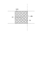
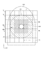
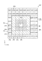
- FIG. 4 is an enlarged plan view of the liquid crystal panel PNL shown in FIG. As shown in FIG. 4, the display unit DA has a region A1 that overlaps with the optical system 2.
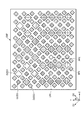
- the pixel PX includes sub-pixels SP1 to SP3.
- the sub-pixel SP1, the sub-pixel SP2, and the sub-pixel SP3 are arranged in the same manner.
- the sub-pixel SP1, the sub-pixel SP2, and the sub-pixel SP3 are repeatedly arranged in this order.
- the color filter CF includes colored layers CFR, CFG, and CFB.
- the sub-pixel SP1 includes a colored layer CFR of the first color.
- the sub-pixel SP2 includes a second color colored layer CFG.
- the sub-pixel SP3 includes a colored layer CFB of a third color.
- the first color colored layer CFR, the second color colored layer CFG, and the third color colored layer CFB are different colors from each other.
- the first color is red (R), the second color is green (G), and the third color is blue (B).
- the first color, the second color, and the third color are shown by way of example and can be deformed in various ways. Any one of the first color, the second color, and the third color may be red, the other color may be green, and the remaining color may be blue. Further, a part of the third color may be, for example, white (W).
- the pixel PPX faces the opening OP1 and is superimposed on the center OX of the optical system 2.
- the pixel PPX is configured without a colored layer.
- the pixel PPX may include a transparent resin layer (referred to as a colored layer CFW).
- the light-shielding layer BM is superimposed on a part of the pixel PPX. In FIG. 4, the light-shielding layer BM superimposed on the pixel PX other than the pixel PPX is not shown.
- the light-shielding layer BM is integrally formed with the light-shielding layer BMA of the non-display portion NDA shown in FIG.
- the light-shielding layer BM has an opening POP.
- the center of the opening POP is superimposed on the center OX of the optical system 2.
- the opening POP and the optical system 2 are concentric circles.
- the opening POP is formed in a circular shape. It is desirable that the opening POP is formed in a perfect circle.
- the pixel PPX may not be used for display, so the term pixel is not correct.
- an electrode having the same transparent conductive film as the pixel that contributes to display, or A pixel is called a pixel including an opening formed in the same light-shielding layer BM as the pixel even if it does not have a transparent conductive film.
- the width of the pixel PPX is substantially the same as the width of the pixel PX.
- the diameter of the opening POP and the width of the pixel PPX are substantially equivalent.
- the diameter of the optical system 2 corresponds to approximately 5 times the diameter of the opening POP.
- the diameter of the optical system 2 is about 3000 ⁇ m, and the diameter of the opening POP is about 600 ⁇ m.
- a pixel BPX for shading is provided adjacent to the pixel PPX.
- the number of pixel LPX adjacent to the pixel PPX is not limited to the above.
- a pixel BPX may be adjacent to the pixel BPX on the opposite side in the direction adjacent to the pixel PPX, and a further pixel BPX may be provided. That is, the pixels BPX may be arranged in a plurality of rows and a plurality of columns.
- the pixel BPX includes sub-pixels BSP1 to BSP3. Similar to the pixel PX, the sub-pixel BSP1, the sub-pixel BSP2, and the sub-pixel BSP3 are arranged in the same manner in any of the pixel BPX.
- the sub-pixels BSP1 to BSP3 are configured with a light-shielding layer BM. As a result, the light from the optical system 2 is blocked by the sub-pixel BSP.
- a pixel LPX for lighting is provided adjacent to the pixel BPX.
- the number of pixel LPXs adjacent to the pixel BPX is not limited to the above, and for example, one pixel LPX may be provided in each of the first direction X and the second direction Y, that is, four pixel LPXs may be provided.
- an additional pixel LPX may be provided on a side that is not adjacent to the pixel BPX. That is, the pixel LPX may be arranged in a plurality of rows and a plurality of columns.
- the pixel LPX includes sub-pixels LSP1 to LSP3. Similar to the pixel PX, the sub-pixel LSP1, the sub-pixel LSP2, and the sub-pixel LSP3 are arranged in the same manner in any of the pixel LPXs.
- the sub-pixels LSP1 to LSP3 are configured without a colored layer.
- the sub-pixels LSP1 to LSP3 may have a transparent resin layer (colored layer CFW) instead of the color filter CF. In either case, the light passing through the sub-pixel LSP is white light.
- a pixel LPX having no colored layer or a transparent resin layer is provided around the pixel PPX having the opening POP. From the periphery of the opening POP, white illumination light is emitted from the pixel LPX to the subject. As a result, the illuminance of the subject imaged by the image pickup device 1 becomes high, and it becomes possible to take a clear picture with the image pickup device 1.
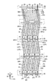
- FIG. 5 is an enlarged plan view of the pixel PPX, the pixel BPX, the pixel LPX, and the pixel PX shown in FIG.
- the direction that intersects the second direction Y at an acute angle clockwise is defined as the direction D1
- the direction that intersects the second direction Y at an acute angle counterclockwise is defined as the direction D2.
- the angle ⁇ 1 formed by the second direction Y and the direction D1 is substantially the same as the angle ⁇ 2 formed by the second direction Y and the direction D2.
- Scanning lines G1 to G4 each extend in the first direction X and are lined up at intervals in the second direction Y.
- the signal lines S1 to S4 extend in the second direction Y, respectively, and are arranged at intervals in the first direction X.
- the scanning line G and the signal line S are metal materials such as aluminum (Al), titanium (Ti), silver (Ag), molybdenum (Mo), tungsten (W), copper (Cu), and chromium (Cr), respectively. , It is formed of an alloy that combines these metal materials.
- the scanning line G and the signal line S may have a single-layer structure or a multi-layer structure, respectively. Note that the scanning line G and the signal line S do not necessarily extend linearly. Well, some of them may be bent. For example, it is assumed that the signal line S extends in the second direction Y even if a part of the signal line S is bent.
- the pixel PX is located between the scanning line G4 and the scanning line G5, and between the signal line S1 and the signal line S4.
- the semiconductor layer SC intersects the scanning line G twice
- the switching element SW is composed of a TFT (thin film transistor) having a double gate structure.
- the switching element SW may be composed of a single-gate structure TFT in which the semiconductor layer SC intersects the scanning line G once.
- the semiconductor layer SC is connected to the signal line S at the connection position P1 and is connected to the pixel electrode PE at the connection position P2.
- the relay electrode is interposed between the pixel electrode PE and the semiconductor layer SC, but the relay electrode is not shown in FIG.
- the pixel electrode PE has a plurality of linear electrodes BR and a slit SL between adjacent linear electrodes BR.
- the linear electrode BR extends along the direction D1.
- the pixel electrode PE has two linear electrodes BR and one slit SL, but the number of linear electrodes BR and slit SL is not limited to this example.
- Each sub-pixel SP is controlled by a signal line S and a scanning line G to which the semiconductor layer SC is connected.
- the sub-pixel SP1 is controlled by the scanning line G5 and the signal line S3
- the sub-pixel SP2 is controlled by the scanning line G5 and the signal line S2
- the sub-pixel SP3 is controlled by the scanning line G5 and the signal line S1.
- the pixel LPX is located between the scanning line G3 and the scanning line G4 and between the signal line S1 and the signal line S4.
- the configuration of each sub-pixel LSP in FIG. 5 is the same as the configuration of the sub-pixel SP. However, in each sub-pixel LSP, the sub-pixel LSP1 is controlled by the scanning line G4 and the signal line S3, the sub-pixel LSP2 is controlled by the scanning line G4 and the signal line S2, and the sub-pixel LSP3 is controlled by the scanning line G4 and the signal line S1. Will be done. Further, the linear electrode BR and the slit SL of each sub-pixel LSP extend along the direction D2.
- the pixel BPX is located between the scanning line G2 and the scanning line G3 and between the signal line S1 and the signal line S4.
- the configuration of each sub-pixel BSP in FIG. 5 is the same as the configuration of the sub-pixel BSP. However, in each sub-pixel BSP, the sub-pixel BSP1 is controlled by the scanning line G3 and the signal line S3, the sub-pixel LSP2 is controlled by the scanning line G3 and the signal line S2, and the sub-pixel LSP3 is controlled by the scanning line G3 and the signal line S1. Will be done. Since the pixel BPX is covered with the light-shielding layer BM as shown in FIG. 4, the light from the pixel BPX is blocked and does not contribute to the display.
- the pixel BPX displays black even when a signal is input from the scanning line and the signal line.
- the pixel BPX may always display black in the off state without inputting a signal, or may be in the on state.
- the semiconductor layer SC may not be provided, that is, the switching element SW may not be provided, and the scanning line G and the signal line S may not be used for control. Even when the switching element SW is not provided, the pixel BPX displays black by the light-shielding layer BM.
- the pixel PPX is located between the scanning line G1 and the scanning line G2, and between the signal line S1 and the signal line S4.
- the pixel PPX includes a pixel electrode PPE.
- the pixel electrode PPE has a plurality of linear electrodes PBR and a slit PSL. In the illustrated example, the linear electrode PBR extends along direction D2.
- the pixel electrode PPE has 6 linear electrodes PBR and 5 slits PSL, but the number of linear electrodes PBR and slit PSL is not limited to this example.
- the signal line S2 extends between the pixel electrode PPE and the scanning line G1, between the pixel electrode PPE and the signal line S1, and between the pixel electrode PPE and the scanning line G2 in a plan view.
- the signal line S3 extends between the pixel electrode PPE and the scanning line G1, between the pixel electrode PPE and the signal line S4, and between the pixel electrode PPE and the scanning line G2 in a plan view.
- the signal lines S2 and S3 extend by bypassing the opening POP. In the present embodiment, the signal lines S2 and S3 are separated from the pixel electrode PPE in a plan view.
- the metal wiring M is superimposed on the signal line S1 and extends along the signal line S1.
- the metal wiring M intersects the signal line S2 in a plan view and is connected to the pixel electrode PPE via the contact hole PCH.
- the pixel electrode PPE is not connected to the scanning line G and the signal line S.
- the pixel PPX is controlled by the metal wiring M.
- the light-shielding layer BM is superimposed on the scanning lines G1 to G4, the signal lines S1 to S4, each sub-pixel LSP, and the semiconductor layer SC of each sub-pixel SP.
- the light-shielding layer BM is located at the opening LOP1 located at the sub-pixel LSP1, the opening LOP2 located at the sub-pixel LSP2, the LOP3 located at the sub-pixel LSP3, and the opening OPR and the sub-pixel SP2 located at the sub-pixel SP1. It has an opening OPG and an opening OPB located in the sub-pixel SP3.
- the light-shielding layer BM covers the sub-pixel BSP1 to the sub-pixel BSP3. Further, the opening POP of the light-shielding layer BM is superimposed on the pixel electrode PPE.
- the first color colored layer CFR shown in FIG. 4 is superimposed on the opening OPR, the second color colored layer CFG is superimposed on the opening OPG, and the third color colored layer CFB is superimposed on the opening OPB.
- the opening LOP1, the opening LOP2, and the opening LOP3 are not provided with the colored layer (color filter CF) as described above.
- a transparent resin layer (colored layer CFW) is provided in the opening LOP1, the opening LOP2, and the opening LOP3.
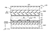
- FIG. 6 is a cross-sectional view of the liquid crystal element LCD along the line AB shown in FIG.
- a liquid crystal element LCD provided with a liquid crystal panel PNL corresponding to a display mode using a transverse electric field between the polarizing plate PL1 and the polarizing plate PL2 will be described.
- the insulating layer 11 is located on the insulating substrate 10.
- the insulating layer 12 is located above the insulating layer 11.
- the scanning line G and the semiconductor layer SC shown in FIG. 5 are located, for example, between the insulating substrate 10 and the insulating layer 11, or between the insulating layer 11 and the insulating layer 12.
- the signal lines S1 and S2 are located on the insulating layer 12 and are covered by the insulating layer 13.
- the metal wiring M is located on the insulating layer 13 and is covered with the insulating layer 14.
- the common electrode CE is located on the insulating layer 14 and is covered by the insulating layer 15.
- the pixel electrode PPE is located on the insulating layer 15 and is covered with the alignment film AL1.
- the contact hole PCH penetrates the insulating layers 14 and 15.
- the pixel electrode PPE faces the common electrode CE via the insulating layer 15.
- the common electrode CE and the pixel electrode PPE are transparent electrodes formed of a transparent conductive material such as ITO or IZO.
- the light-shielding layer BM is located directly above the metal wiring M and directly above the pixel electrode PPE.
- the color filter CF is located directly above the signal line S1.
- the light-shielding layer BM is in contact with the transparent layer OC.
- the light-shielding layer BM is in contact with the transparent layer OC.
- the light-shielding layer BM is in contact with the transparent layer OC or in contact with the transparent resin layer arranged at the position of the color filter CF.
- the light-shielding layer BM is in contact with the color filter CF.
- the insulating substrate 20 is in contact with the transparent layer OC at the opening POP.
- the drive unit DR1 applies a voltage to the metal wiring M to control the transmittance of the liquid crystal element LCD in the pixel PPX.
- the transmittance of the liquid crystal element LCD is controlled according to the magnitude of the voltage applied to the liquid crystal layer LC.
- the drive unit DR1 is electrically connected to the IC chip 6.
- the liquid crystal molecules LM contained in the liquid crystal layer LC are initially arranged in a predetermined direction between the alignment films AL1 and AL2. Oriented. That is, the pixel PPX has the minimum transmittance and displays black. That is, the liquid crystal element LCD exhibits a light-shielding function in the pixel PPX.
- the liquid crystal molecules LM move in a direction different from the initial orientation direction due to the electric field formed between the pixel electrode PPE and the common electrode CE. It is oriented and its orientation direction is controlled by the electric field.
- the liquid crystal element LCD displays white or becomes transparent at the maximum transmittance in the pixel PPX in the on state. That is, the liquid crystal element LCD exhibits a translucent function in the pixel PPX.
- 7 (A) and 7 (B), 8 and 9 are cross-sectional views of a liquid crystal element LCD including the pixel LPX, the pixel PX and the pixel BPX shown in FIG. 5, respectively.
- 7 (A) and 7 (B) are cross-sectional views of the liquid crystal element LCD along the CD line shown in FIG.
- FIG. 8 is a cross-sectional view of the liquid crystal element LCD along the line EF shown in FIG.
- FIG. 9 is a cross-sectional view of the liquid crystal element LCD along the line GH shown in FIG.
- the insulating layers 12 to 14 and the signal line S are not shown.
- the pixel electrode PE is located on the insulating layer 15 and is covered with the alignment film AL1.
- the pixel electrode PE is a transparent electrode formed of a transparent conductive material such as ITO or IZO.
- the colored layer is not arranged at the position facing the pixel electrode PE on the second substrate SUB2.
- a colored layer CFW which is a transparent resin layer is provided in place of the colored layer so as to face the pixel electrode PE.
- the drive unit DR2 for driving the liquid crystal element LCD includes, for example, a scan line drive circuit electrically connected to the scan line G and a signal line drive circuit electrically connected to the signal line S shown in FIG. Includes.
- the drive unit DR2 outputs a signal necessary for irradiating the irradiation light to each pixel LPX of the display unit DA, and controls the transmittance of the liquid crystal element LCD.
- the drive unit DR2 is electrically connected to the IC chip 6.
- the liquid crystal element LCD is not irradiated with the irradiation light in the pixel LPX in the off state.
- the liquid crystal element LCD is irradiated with white irradiation light in the pixel LPX in the on state.
- a second color colored layer CFG is provided on the second substrate SUB2 so as to face the pixel electrode PE.
- the colored layer CFR of the first color and the colored layer CFB of the third color also face each other pixel electrode PE (not shown).
- the drive unit DR2 outputs a signal required for image display to each pixel PX of the display unit DA, and controls the transmittance of the liquid crystal element LCD.
- the liquid crystal element LCD displays black in the pixel PX in the off state.
- the on state where a voltage is applied to the liquid crystal layer LC a part of the light guided to the pixel PX passes through the polarizing plates PL1 and PL2.
- the liquid crystal element LCD displays the color corresponding to the color filter CF in the pixel PX in the on state.
- the above example corresponds to the so-called normally black mode in which black is displayed in the off state, but a normally white mode in which black is displayed in the on state (white is displayed in the off state) may be applied.
- a light-shielding layer BM is arranged at a position facing the pixel electrode PE on the second substrate SUB2. Since the pixel BPX is covered with the light-shielding layer BM in this way, it is always displayed in black.
- the light-shielding pixel BPX displays black no matter what signal is input as described above. That is, even when the same signal as the pixel PX is input to the pixel BPX, black is displayed. Therefore, the pixel BPX may not be controlled independently, but the pixel BPX may be controlled by the same signal as the pixel PX.
- Such a liquid crystal element LCD can function as a pinhole for adjusting the amount of light incident on the camera 1 by transmitting light in the pixel PPX and blocking light in the other pixel BPX and the pixel PX superimposed on the optical system 2. can.
- the influence of aberration in the optical system 2 can be reduced, the sharpness can be improved, and the depth of focus can be increased.
- the distance between the camera 1 and the subject is several cm, the resolving power of the camera 1 is improved, and a clear photograph can be taken at a close distance to the subject.
- a fingerprint can be taken for fingerprint authentication.
- an infrared camera may be also provided to take a picture of the vein.
- the electronic device described above has a pixel LPX having no colored layer or a transparent resin layer around the pixel PPX having the opening POP.
- White irradiation light is emitted from the periphery of the opening to the subject through the pixel LPX.
- the illuminance of the subject captured by the imaging device 1 can be increased, and a clear photograph can be taken by the imaging device 1.
- FIG. 10 is a plan view showing another configuration example of the opening POP in the present embodiment.
- the configuration example shown in FIG. 10 is different from the configuration example shown in FIG. 4 in that it includes a plurality of openings POP2.
- the pixel PPX shown in FIG. 10 has a plurality of opening POPs 2 evenly arranged in the pixel PPX as opening POPs.
- One opening POP2 is formed in a circular shape. It is desirable that the opening POP2 is formed in a perfect circle.
- the diameter of the opening POP2 is smaller than the diameter of the opening POP shown in FIG.
- the opening POP2 does not necessarily have to be superimposed on the center OX of the optical system 2, but it is preferably arranged at a position symmetrical with respect to the center OX.
- the amount of light incident on the light receiving surface of the image pickup apparatus 1 is increased, and a clearer photograph can be taken.
- FIG. 11 is a plan view showing another configuration example of the sub-pixel LSP in the present embodiment.
- the configuration example shown in FIG. 11 is different from the configuration example shown in FIG. 5 in that the sub-pixel LSP of the pixel LPX is larger than the sub-pixel SP of the pixel PX.
- the pixel LPX shown in FIG. 11 has one sub-pixel LSP.
- the pixel LPX is located between the scanning line G3 and the scanning line G4 and between the signal line S1 and the signal line S4.
- the pixel LPX (sub-pixel LSP) is controlled by the scanning line G4 and the signal line S3.
- the pixel LPX shown in FIG. 11 has five linear electrodes BR and four slits SL, but the number of linear electrodes BR and slit SL is not limited to this example.
- the pixel LPX (sub-pixel LSP) shown in FIG. 11 has, for example, about 2.5 times the width in the first direction X as compared with the sub-pixel SP of the pixel PX, and the size of the opening LOP is also the same as that of the opening OP. It is about 2.5 times as much as the comparison.
- the length in the first direction X is long has been described, but the length in the second direction Y may be increased. Further, the length in both the first direction X and the second direction Y may be increased.
- the irradiation light emitted from the pixel LPX to the subject may be monochromatic light.
- FIG. 12 shows a cross-sectional view of the pixel LPX.
- the pixel LPX shown in FIG. 12 has a single color, for example, a blue colored layer CFB as a color filter CF.
- the irradiation light emitted from the pixel LPX to the subject is blue light.
- the color of the colored layer is not limited to blue, and other colors such as red and green may be selected according to the sensitivity of the image pickup apparatus 1.
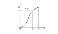
- FIG. 13 is a diagram showing the relationship of brightness with respect to the applied voltage in the pixel LPX and the pixel PX in the present embodiment.
- the configuration example shown in FIG. 13 is different from the configuration example shown in FIG. 3 in that the voltage applied to the pixel LPX is larger than the voltage applied to the pixel PX.
- the voltage applied to the pixel LPX and the voltage applied to the pixel PX are the voltage Vsig applied to the signal line S of the pixel LPX and the signal line S of the pixel PX, that is, an image signal, respectively.
- the pixel PX displays the off state (luminance L0), that is, black when the voltage Vsig is the voltage V0, and displays the luminance L1, that is, white with respect to the maximum transmittance when the voltage Vsig is the maximum voltage V1.
- the liquid crystal element LCD of this configuration example is driven in the so-called normally black mode.
- FIG. 14 is a diagram showing another configuration example of the liquid crystal panel PNL of the present embodiment.
- the brightness of the irradiation light of the light source EM1 is increased during the subject shooting period, and the voltage applied to the pixel PX is made smaller than that of the pixel LPX, as compared with the configuration example shown in FIG. It is different in that.
- FIG. 14 (A) and 14 (B) show the configuration of the liquid crystal panel PNL during the subject non-shooting period (display only) and the subject shooting period, respectively.
- the irradiation light of the brightness Li1 from the light source EM1 is incident on the light guide plate LG1 of the liquid crystal panel PNL.
- the pixel PX modulates the incident light according to the voltage V3 applied from the drive unit DR2 via the signal line S, and emits light having a brightness L3 to display an image.
- the irradiation light of the brightness Li2 from the light source EM1 is incident on the light guide plate LG1 of the liquid crystal panel PNL.
- the brightness Li2 is larger than the brightness Li1 during the non-shooting period.
- the drive unit DR2 applies a voltage V4 to the pixel PX and a voltage V5 to the pixel LPX via the signal line S.
- the voltage V4 is smaller than the voltage V3.
- the voltage V5 is equal to the voltage V3 applied to the pixel PX during the non-photographing period.
- the pixel PX modulates the incident light according to the voltage V4 and emits the light having the brightness L4 to display the image.
- the drive unit DR2 determines the magnitude of the voltage V4 so that the brightness L3 in the subject non-shooting period and the brightness L4 in the subject shooting period in the pixel PX are equal to each other.
- the present invention is not limited to this. Even during the non-shooting period, the voltage V3 may be applied to turn on the pixel PX as in the case of the pixel PX.
- FIG. 15 is a diagram showing another configuration example of the liquid crystal panel PNL of the present embodiment.
- the liquid crystal panel PNL has a sensor that detects the proximity or contact of the subject, and the pixel LPX only when the subject is close or in contact. It differs in that it increases the brightness of the.
- FIG. 15 shows the configuration of a liquid crystal panel PNL having a sensor SEN that detects the proximity or contact of a subject.
- the sensor SEN is, for example, a capacitive touch sensor, an optical touch sensor, or an electromagnetic induction touch sensor.
- the sensor SEN may be provided inside the liquid crystal panel PNL, or may be a sensor that is arranged outside the liquid crystal panel PNL and superimposes on the pixel PX, the pixel LPX, and the pixel PPX.
- the drive unit DR2 applies a voltage Vsig so that the brightness of the pixel LPX becomes larger than the brightness of the pixel PX as described above.
- the pixel LPX is driven in the same manner as in FIG. 14 (A). That is, the drive unit DR2 is turned off without applying a voltage to the pixel LPX. Alternatively, the drive unit DR2 applies a voltage similar to that of the pixel PX to the pixel LPX to perform a normal display.
- high-intensity illumination light can be emitted from the pixel LPX only when the subject FNG is in close proximity to or in contact with the subject. That is, in the image display in a state where the subject FNG is in close proximity or not in contact with the subject FNG, high-intensity illumination light is not emitted from the pixel LPX. This further improves the visibility of the liquid crystal panel PNL.
- a light receiving element such as a photoelectric conversion element may be provided instead of the image pickup device 1. Even when the light receiving element is provided, the brightness of the pixel LPX is increased, so that the sensitivity of the light receiving element is increased.
- FIG. 16 is a diagram showing another configuration example of the pixel LPX of the present embodiment.
- the configuration example shown in FIG. 16 is different from the configuration example shown in FIG. 5 in that a plurality of pixel LPXs are driven by the same signal line and the same scanning line.
- the signal line S shown in FIG. 16 has a circular signal line SL1 and a linear signal line SL2.
- the signal line SL1 is arranged concentrically with the opening POP in a plan view.
- the scanning line G shown in FIG. 16 has a circular scanning line GL1 and a linear scanning line GL2.
- the scanning lines GL1 are arranged concentrically with the opening POP in a plan view. That is, the scanning line GL1 and the signal line SL1 are arranged concentrically.
- the scanning lines GL1 and GL2, and the signal lines SL1 and GL2 are not connected to the other scanning lines G and the other signal lines S, respectively, and are independently driven by the driving unit DR2.
- Each of the plurality of pixel LPXs is arranged concentrically with the opening POP.
- the signal line SL1 and the scanning line GL1 are electrically connected to a plurality of pixels LPX. This makes it possible to drive the plurality of pixels LPX at the same time.
- the scanning line G and the signal line S shown in FIG. 16 and the plurality of pixels LPX are arranged in a circular shape, but the shape is not limited to this, and may be arranged in a quadrangular shape, for example. Further, a plurality of pixel LPXs may be arranged adjacent to the plurality of pixel LPXs arranged concentrically with the opening POP and on the side opposite to the pixel PPX. Further arranged pixels LPX are driven by a signal line S and a scanning line G different from the signal line SL1 and the scanning line GL1. In other words, the plurality of pixel LPXs may be arranged concentrically with respect to the opening POP, in duplicate or more.
- FIG. 17 is a plan view showing another configuration example of the pixel layout in the present embodiment.
- the configuration example shown in FIG. 17 is different from the configuration example shown in FIG. 4 in that it has the sub-pixel SP4 having the colored layer CFW which is a transparent resin layer.
- the sub-pixels SP1 and SP4 are repeatedly arranged in the first direction X, while the sub-pixels SP2 and the sub-pixels SP3 are repeatedly arranged.
- the sub-pixels SP1 and SP2 are repeatedly arranged, while the sub-pixels SP3 and SP4 are repeatedly arranged.
- the sub-pixels SP1 to SP4 are arranged so that the sub-pixels of the same type are not continuously arranged in the first direction X and the second direction Y.
- the pixel PX in the pixel PX in which the pixel PPX is located, the pixel PX is formed without the sub-pixel SP4.
- the pixel PPX originally occupies an area of the pixel PX in which the sub-pixel SP4 is arranged. In other words, the pixel PPX occupies an area equivalent to one sub-pixel SP.
- a pixel BPX for shading is provided adjacent to the pixel PPX.
- the pixel BPX occupies the area corresponding to one sub-pixel SP, the pixel BPX is also referred to as a sub-pixel BSP.
- the pixel BPX is covered with a light-shielding layer BM as described above.
- the pixel BPX may be provided with a further pixel BPX adjacent to the pixel BPX on the opposite side in the direction adjacent to the pixel PPX. That is, the pixel BPX (sub-pixel BSP) may be arranged in a plurality of rows and a plurality of columns.
- a pixel LPX for lighting is provided adjacent to the pixel BPX.
- the pixel LPX occupies the area corresponding to one sub-pixel SP, the pixel LPX is also referred to as a sub-pixel LSP.
- the pixel LPX is not provided with the color filter CF as described above, or is provided with a transparent resin layer (colored layer CFW).
- the pixel LPX may be provided with a pixel LPX adjacent to the pixel LPX on the opposite side in the direction adjacent to the pixel BPX. That is, the pixel LPX (sub-pixel LSP) may be arranged in a plurality of rows and a plurality of columns.
- FIG. 18 is a plan view showing the pixel PPX, the pixel BPX, the pixel LPX, and the sub-pixel SP1 shown in FIG.
- the pixel electrode PE of the pixel BPX is between the signal line S2 and the signal line S3
- the pixel electrode PE of the pixel LPX is between the signal line S3 and the signal line S4
- the pixel electrode PE of the sub-pixel SP1. Is located between the signal line S4 and the signal line S5.
- the pixel BPX, the pixel LPX, and the pixel electrode PE of the sub-pixel SP1 are located between the scanning line G1 and the scanning line G2.
- the pixel electrode PPE is located between the signal line S1 and the signal line S2, and between the scanning line G1 and the scanning line G2.
- the pixel electrode PE1 has four linear electrodes BR and three slits SL
- the pixel electrode PPE has four linear electrodes PBR and three slits PSL.
- FIG. 19 is a plan view showing another configuration example of the pixel layout in the present embodiment.
- the configuration example shown in FIG. 19 is different from the configuration example shown in FIG. 17 in that it does not have a pixel LPX for illumination.
- a pixel PX (sub-pixel SP) is provided adjacent to the pixel PPX.
- the illuminance of the subject imaged by the image pickup apparatus 1 can be further increased by the light emitted from the sub-pixel SP around the pixel PPX.
- a pixel BPX (sub-pixel BSP) for shading may be provided between the pixel PPX and the pixel PX.
- FIG. 20 is a perspective view showing the configuration of the electronic device 100 of the present embodiment.
- the display device is an organic electroluminescence (EL) display device.
- the electronic device 100 includes an image pickup device 1, a display panel DSP, a wiring board PB1, a wiring board PB2, and a support member SUS.
- the display panel DSP includes a flat plate-shaped first substrate SUB1 and a flat plate-shaped polarizing plate POL arranged to face the first substrate SUB1.
- the display panel DSP is an organic EL panel.
- the display panel DSP includes a display unit DA that displays an image and a non-display unit NDA that surrounds the display unit DA.
- the display panel DSP includes a pixel PPX and a plurality of pixel PX in the display unit DA.
- the plurality of pixels PX are arranged in the first direction X and the second direction Y and are provided in a matrix. Similar to FIG. 1, the pixel PPX is superimposed on the central OX of the optical system 2 of the image pickup apparatus 1.
- the first substrate SUB1 has a pad region MT located outside the region overlapping the polarizing plate POL.
- the wiring board PB1 is mounted above the pad region MT in the non-display portion NDA.
- the length of the side edge parallel to the first direction X of the wiring board PB1 is smaller than the length of the side edge parallel to the first direction X of the first substrate SUB1 and the polarizing plate POL. It may be equivalent.
- the display panel DSP and the wiring board PB1 are electrically connected to each other.
- the wiring board PB2 is arranged below the wiring board PB1.
- the wiring board PB1 and the wiring board PB2 are, for example, flexible boards having flexibility. Although two wiring boards PB1 and PB2 are shown in FIG. 20, only one wiring board may be used.
- the electronic device 100 shown in FIG. 20 has a bending region BA which is a region that can be bent when it is housed in the housing.
- the support member SUS is located below the display panel DSP and is attached to the first substrate SUB1.
- the support member SUS is not arranged at a position overlapping the bending region BA in the third direction Z. When it is not necessary to bend the electronic device 100, it is not necessary to provide the bending region BA and the support member SUS.
- the wiring boards PB1 and PB2 may be rigid flexible boards having a rigid part and a flexible part formed of a hard material. Further, one wiring board may be provided without providing the two wiring boards PB1 and PB2.
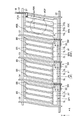
- FIG. 21 is a plan view showing the circuit configuration of the display panel DSP.
- the display panel DSP includes a first insulating substrate 110, a plurality of organic EL element OLEDs arranged on the first insulating substrate 110, various wirings, gate drivers GD1 and GD2, and a selection circuit. It has SD and.
- the organic EL element OLED includes an organic EL element OLED1 exhibiting a first color, an organic EL element OLED2 exhibiting a second color, an organic EL element OLED3 exhibiting a third color, and an organic EL element exhibiting a fourth color.
- OLED4 is included.
- the first color is red
- the second color is green
- the third color is blue
- the fourth color is white.
- the organic EL element OLED includes a light emitting element and a pixel circuit for supplying a driving current to the organic light emitting layer to drive the organic light emitting layer.
- the pixel circuit includes a drive transistor and various switching elements described later.
- FIG. 21 illustrates a plurality of control wiring SSGs and a plurality of image signal line VLs as a part of various wirings.
- the gate drivers GD1 and GD2 and the selection circuit SD are located in the non-display unit NDA.
- the control wiring SSG and the image signal line VL are electrically connected to the organic EL element OLED.
- the control wiring SSG is electrically connected to the gate drivers GD1 and GD2 by the non-display unit NDA.
- the image signal line VL is electrically connected to the selection circuit SD by the non-display unit NDA.
- Various signals and voltages are given to the gate drivers GD1 and GD2 and the selection circuit SD from the panel driver PDV.
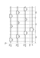
- the organic EL element OLED includes a light emitting element ELM and a pixel circuit PC that supplies a drive current to the light emitting element ELM.
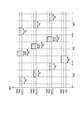
- the pixel circuit PC is electrically connected to the pixel electrode PE described later.
- the pixel circuit PC includes a drive transistor DRT, a pixel transistor SST, an output transistor BCT, a holding capacitance Cs, and an auxiliary capacitance CAD as a plurality of elements.
- the output transistor BCT may be shared by a plurality of organic EL elements OLEDs as described later.
- One output transistor BCT shown in FIG. 22 is arranged with respect to the organic EL element OLED.
- the gate driver GD1 includes a reset transistor RST.
- each transistor is an Nch TFT.
- the element capacitance Cled shown in FIG. 22 is the internal capacitance of the light emitting element ELM, and is the capacitance between the anode and the cathode.
- the reset transistor RST, the pixel transistor SST, and the output transistor BCT do not have to be composed of transistors.
- the reset transistor RST, the pixel transistor SST, and the output transistor BCT may function as a reset switch, a pixel switch, and an output switch, respectively.
- one of the source electrode and the drain electrode of the transistor will be the first electrode, and the other will be the second electrode. Further, one electrode of the capacitive element is used as a first electrode, and the other electrode is used as a second electrode.
- the drive transistor DRT, the pixel electrode PE, and the light emitting element ELM are connected in series between the first power supply line VDDL and the second power supply line VSSL.
- the first power supply line VDDL is held at a constant potential
- the second power supply line VSSL is held at a constant potential different from the potential of the first power supply line VDDL.
- the potential P VDD of the first power supply line VDDL is higher than the potential PVSS of the second power supply line VSSL.
- the first electrode of the drive transistor DRT is electrically connected to the anode of the light emitting element ELM, the holding capacity Cs, and the auxiliary capacity CAD.
- the drive transistor DRT is configured to control the current value to the light emitting element ELM.
- the second electrode of the drive transistor DRT is electrically connected to the first electrode of the output transistor BCT.
- the first electrode of the pixel transistor SST is electrically connected to the gate electrode of the drive transistor DRT and the second electrode of the holding capacity Cs.
- the second electrode of the pixel transistor SST is electrically connected to the image signal line VL.
- the second electrode of the output transistor BCT is electrically connected to the first power supply line VDDL. Further, the cathode of the light emitting element is electrically connected to the second power supply line VSSL.
- the reset transistor RST is provided in the gate driver GD1, and the first electrode of the reset transistor RST is electrically connected to the reset wiring SV.
- the second electrode of the reset transistor RST is electrically connected to the reset power supply line RL.
- the voltage Vsig which is an image signal, is supplied to the image signal line VL, and the reset power supply line RL is set to the reset power supply potential Vrst.
- the voltage Vsig is a signal written in the organic EL element OLED.
- the gate electrode of the output transistor BCT is electrically connected to the control wiring SBG.
- An output control signal BG is supplied to this control wiring SBG.
- the gate electrode of the pixel transistor SST is electrically connected to the control wiring SSG.
- a pixel control signal SG is supplied to this control wiring SSG.
- the gate electrode of the reset transistor RST is electrically connected to the control wiring SRG.
- a reset control signal RG is supplied to this control wiring SRG.
- the transistors other than the drive transistor DRT may be PchTFTs, and NchTFTs and PchTFTs may be mixed.
- the drive transistor DRT may be a Pch TFT.
- the current may flow through the light emitting element ELM in the opposite direction to the present embodiment.
- the auxiliary capacitance CAD may be coupled to the first electrode on the drive transistor DRT side of the electrodes of the light emitting element ELM.
- circuit configuration described in FIG. 22 is an example, and other configurations may be used. For example, a part of the circuit configuration described with reference to FIG. 22 may be omitted, or another configuration may be added.
- FIG. 23 is a schematic view showing a cross section showing the display unit DA of the display panel DSP shown in FIG. 20.
- the first substrate SUB1 includes a first insulating substrate 110, a transistor Tr1, a transistor Tr2, a transistor Tr3, a transistor Tr4, a light reflecting layer RFL, an organic EL element OLED1, an organic EL element OLED2, and an organic EL element OLED3.
- the first insulating substrate 110 is formed by using an organic insulating material, for example, by using polyimide. Therefore, it may be more appropriate to refer to the first insulating substrate 110 as an organic insulating substrate (resin substrate). Alternatively, it may be more appropriate to refer to the first insulating substrate 110 as an insulating layer, an organic insulating layer, or a resin layer.
- the first insulating substrate 110 has a first surface 110A and a second surface 110B opposite to the first surface 110A.
- the first insulating substrate 110 is covered with the first insulating film 111.
- the transistors Tr1, Tr2, and Tr3 are formed above the first insulating film 111.
- the transistors Tr1, Tr2, Tr3, and Tr4 are composed of a top gate type thin film transistor, but may be composed of a bottom gate type thin film transistor.
- the transistors Tr1 to Tr4 correspond to the drive transistor DRT of FIG. Since the transistors Tr1, Tr2, Tr3, and Tr4 have the same configuration, the structure thereof will be described in more detail below with a focus on the transistor Tr1.
- the transistor Tr1 includes a semiconductor layer SC formed on the first insulating film 111.
- the semiconductor layer SC is covered with the second insulating film 112.
- the second insulating film 112 is also arranged on the first insulating film 111.
- the gate electrode WG of the transistor Tr1 is formed on the second insulating film 112 and is located directly above the semiconductor layer SC.
- the gate electrode WG is covered with a third insulating film 113.
- the third insulating film 113 is also arranged on the second insulating film 112.
- Such a first insulating film 111, a second insulating film 112, and a third insulating film 113 are formed of, for example, an inorganic material such as silicon oxide or silicon nitride.
- the source electrode WS and drain electrode WD of the transistor Tr1 are formed on the third insulating film 113.
- the source electrode WS and the drain electrode WD are electrically connected to the semiconductor layer SC through contact holes penetrating the second insulating film 112 and the third insulating film 113, respectively.
- the transistor Tr1 is covered with a fourth insulating film 114.
- the fourth insulating film 114 is also arranged on the third insulating film 113.
- Such a fourth insulating film 114 is formed of, for example, an organic material such as a transparent resin.
- the light reflecting layer RFL is arranged on the fourth insulating film 114.
- the light reflecting layer RFL is formed of a metal material having high light reflectance such as aluminum and silver.
- the surface of the light reflecting layer RFL (that is, the surface on the polarizing plate POL side) may be a flat surface or an uneven surface for imparting light scattering property.
- the organic EL layers OL1 to OL4 are formed on the fourth insulating film 114.
- the organic EL layer OL1 is electrically connected to the transistor Tr1
- the organic EL layer OL2 is electrically connected to the transistor Tr2
- the organic EL layer OL3 is electrically connected to the transistor Tr3, and the organic EL layer
- the OL1 is electrically connected to the transistor Tr4.
- Organic EL layer OL1 Each of the organic EL layers OL1 to OL4 is configured as a so-called top emission type that emits light toward the side of the polarizing plate POL. In FIG.
- the organic EL element OL1 and the transistor Tr1 are combined to form the organic EL element OLED1
- the organic EL layer OL2 and the transistor Tr2 are combined to form the organic EL element OLED2
- the organic EL layer OL3 and the transistor Tr3 are combined to form the organic EL element OLED3.
- the organic EL layer OL4 and the transistor Tr4 are combined to form an organic EL element OLED4. When it is not necessary to distinguish the organic EL elements OLED1 to OLED4, they are simply referred to as organic EL elements OLED.
- the organic light emitting layer ORG of the organic EL layers OL1 to OL4 emits white light.
- the emitted light passes through the color filter CF provided on the organic EL layers OL1 to OL4, and emits light toward the side of the polarizing plate POL.
- the color filter CF has a first color colored layer CFR, a second color colored layer CFG, a third color colored layer CFB, and a fourth color colored layer CFW.
- the first color is red (R)
- the second color is green (G)
- the third color is blue (B)
- the fourth color is white (W).
- the white light emitted from the organic EL layers OL1 to OL4 passes through the colored layer CFR, the colored layer CFG, the colored layer CFB, and the colored layer CFW which is a transparent resin layer, and is used as red light, green light, blue light, and white light, respectively. It is emitted upward.
- the pixel PPX facing the image pickup apparatus 1 and the pixel LPX for illumination have a configuration having a colored layer CFW which is a transparent resin layer, that is, a configuration similar to that of the organic EL element OLED4.
- the organic EL layer OL1 includes a pixel electrode PE1 formed on the light reflecting layer RFL.
- the pixel electrode PE1 is in contact with the drain electrode WD of the transistor Tr1 and is electrically connected to the transistor Tr1.
- the organic EL layer OL2 includes a pixel electrode PE2 electrically connected to the transistor Tr2
- the organic EL layer OL3 includes a pixel electrode PE3 electrically connected to the transistor Tr3
- the organic EL layer OL4 includes the transistor Tr4. It is provided with a pixel electrode PE4 electrically connected to the device.
- the pixel electrodes PE1, PE2, PE3, and PE4 are formed of, for example, a transparent conductive material such as ITO or IZO.
- a partition wall insulating layer BK is provided on the fourth insulating film 114 and the pixel electrode PE.
- the partition wall insulating layer BK is provided with an opening at a position corresponding to the pixel electrode PE, or is provided with a slit at a position corresponding to a column or row formed by the pixel electrode PE.
- the partition wall insulating layer BK has an opening at a position corresponding to the pixel electrode PE.
- the organic EL layers OL1 to OL4 further include an organic light emitting layer ORG and a common electrode CE.
- an organic light emitting layer ORG is located on the pixel electrodes PE1 to PE4, respectively. Further, the organic light emitting layer ORG is located between the adjacent partition wall insulating layer BK. As described above, the organic light emitting layer ORG is an organic light emitting layer that emits white light.
- the above-mentioned light emitting element ELM corresponds to a pixel electrode PPE, an organic light emitting layer ORG, and a common electrode CE.
- the common electrode CE is located on the organic light emitting layer ORG and the partition wall insulating layer BK.
- the common electrode CE is formed of, for example, a transparent conductive material such as ITO or IZO.
- the organic EL layers OL1 to OL4 are each partitioned by a partition wall insulating layer BK. Although not shown, it is desirable that the organic EL layers OL1 to OL4 are sealed with a transparent sealing film.
- the organic EL element OLED may be configured as a so-called bottom emission type that radiates light toward the side of the first insulating substrate 110. In this case, various adjustments are made such as the position of the light reflecting layer RFL.
- the sealing layer SLI covers the organic EL layers OL1 to OL4.
- the sealing layer SLI is formed so as to seal a member arranged between the first insulating substrate 110 and the sealing layer SLI.
- the sealing layer SLI suppresses the invasion of oxygen and water into the organic EL layers OL1 to OL4, and suppresses the deterioration of the organic EL layers OL1 to OL4.
- the sealing layer SLI may be composed of a laminate of an inorganic film and an organic film.
- a colored layer CFR, a colored layer CFG, a colored layer CFB, a colored layer CFW, and a light-shielding layer BMB are provided on the sealing layer SLI.
- the light-shielding layer BMB is provided above the transistors Tr1 to Tr4.
- the colored layer CFR is provided on the organic light emitting layer ORG of the organic EL element OLED1 between the colored layer CFR and the adjacent light-shielding layer BMB.
- the colored layer CFG is provided on the organic light emitting layer ORG of the organic EL element OLED2 between the colored layer CFG and the adjacent light-shielding layer BMB.
- the colored layer CFB is provided on the organic light emitting layer ORG of the organic EL element OLED3 between the colored layer CFB and the adjacent light shielding layer BMB.
- the colored layer CFW is provided on the organic light emitting layer ORG of the organic EL element OLED4 with the adjacent light-shielding layer BMB.
- the ends may overlap in the third direction Z, respectively.
- the pixel PPX and the pixel LPX have a structure having a colored layer CFW which is a transparent resin layer.
- the colored layer CFW of the pixel PPX corresponds to the above-mentioned opening POP. It can be said that the opening POP of the present embodiment is an opening provided between the light-shielding layers BMB of the organic EL element OLED adjacent to the pixel PPX.
- the pixel PPX may have a plurality of opening POPs evenly arranged in the pixel PPX as the opening POP.
- a fifth insulating film 115 is provided on the colored layer CFR, the colored layer CFG, the colored layer CFB, the colored layer CFW, and the light-shielding layer BMB.
- the fifth insulating film 115 is formed of a resin material such as polyimide or acrylic. Further, it may be formed of an inorganic material such as a silicon oxide layer.
- the polarizing plate POL is arranged above the fifth insulating film 115.
- the polarizing plate POL is adhered to the fifth insulating film 115 by the adhesive layer AD5.
- a resin layer or an optical film may be provided between the fifth insulating film 115 and the polarizing plate POL.
- a member such as an optical film or a glass substrate may be provided above the polarizing plate POL.
- the pixel PX shown in FIG. 21 is, for example, the smallest unit that constitutes a color image, and includes the above-mentioned organic EL elements OLED1 to OLED4.
- FIG. 23 describes a configuration in which the organic EL element OLED4 that irradiates white light is provided, but the present invention is not limited to this.
- the display panel DSP of the present embodiment may have only the organic EL elements OLED1 to OLED3 without providing the organic EL element OLED4. That is, the display panel DSP of the present embodiment may be a display panel composed of an RGB organic EL element OLED.
- the pixel PPX and the pixel LPX are organic EL elements provided with a colored layer CFW which is a transparent resin layer.
- FIG. 24 is a timing chart showing output examples of various signals related to the reset operation, offset cancel operation, write operation, and light emission operation in the organic EL element OLED.
- signals supplied to the control wiring SRG, the control wiring SBG, the control wiring SIG, and the control wiring SSG will be mainly described.
- the reset operation and the offset cancel operation in the organic EL element OLED shall be performed in units of two lines of the organic EL element OLED.
- FIG. 23 regarding the control wiring electrically connected to the two rows of organic EL element OLEDs (hereinafter referred to as the first row and the second row organic EL element OLEDs) that are the targets of the reset operation and the offset cancel operation.
- the reset control signal given to the control wiring SRG is shown as RG12
- the output control signal given to the control wiring SBG is shown as BG12.
- the pixel control signal given to the control wiring SSG electrically connected to the organic EL element OLED in the first line is given to the control wiring SSG electrically connected to the organic EL element OLED in the first and second lines.
- the pixel control signal is shown as SG2.
- FIG. 24 shows the timing of various signals for the organic EL element OLEDs in the first and second rows, but the same applies to, for example, the organic EL element OLEDs in the third and subsequent rows.
- the writing operation of the voltage Vsig of the image signal will be described.
- the pixel control signal SG is switched from the L level to the H level.
- the pixel transistor SST can be switched to the on state.
- the voltage Vsig of the image signal is written to the gate electrode of the drive transistor DRT through the pixel transistor SST.
- the writing to the organic EL element OLED on the first line is completed, the writing to the organic EL element OLED on the second line is performed in the same manner.
- the pixel transistor SST is turned off for the organic EL element OLED on the first line.
- a light emitting operation for causing the light emitting element ELM to emit light will be described.
- the pixel control signal SG is switched from the H level to the L level.
- the pixel transistor SST is switched to the off state.
- FIG. 25 is a plan view showing the pixel layout in the present embodiment.
- FIG. 25 is equivalent to replacing the sub-pixels SP1 to SP4 of FIG. 17 of the first embodiment with the organic EL elements OLED1 to OLED4. Therefore, the description of FIG. 25 is based on the description of FIG. 17, and the details will be omitted.
- FIG. 26 is another plan view showing the pixel layout in the present embodiment.
- FIG. 26 shows a pixel layout having the organic EL elements OLED1 to OLED3.
- the direction that intersects the acute angle ⁇ a clockwise with respect to the second direction Y is defined as the direction DX
- the direction perpendicular to the direction DX is defined as the direction DY.
- the organic EL element OLED1 is adjacent to the organic EL element OLED2 in the direction DX and the direction DY.
- the organic EL elements OLED2 are adjacent to each other in the first direction X, and are adjacent to each other in the second direction Y as well.
- the organic EL element OLED2 adjacent to the organic EL element OLED1 in the direction DX is adjacent to the organic EL element OLED3 in the direction DY.
- the organic EL element OLED2 adjacent to the organic EL element OLED3 in the direction DX is adjacent to the organic EL element OLED1 in the direction DY.
- the organic EL element OLED3 is adjacent to the organic EL element OLED2 in the direction DX and the direction DY.
- the pixel PPX occupies an area in which one of the organic EL elements OLED3 is arranged.
- the pixel PPX may occupy not the area where the organic EL element OLED3 is arranged but the area where one of the organic EL element OLED1 is arranged or the area where one of the organic EL element OLED2 is arranged. ..
- the pixel BPX is provided adjacent to the pixel PPX in the direction DX and the direction DY.
- the pixel BPX may not be provided, and the pixel LPX may be provided adjacent to the pixel PPX.
- the pixel BPX in FIG. 26 occupies an area in which one organic EL element OLED is arranged.
- the pixel LPX is provided adjacent to the pixel BPX in the direction DX and the direction DY.
- the pixel LPX has the same configuration as the organic EL element OLED4. That is, the pixel LPX is provided with a colored layer CFW and emits white light.
- the pixel LPX in FIG. 23 occupies the area where one organic EL element OLED is arranged.
- the electronic device described in this embodiment has a pixel LPX having a transparent resin layer around the pixel PPX having an opening.
- White irradiation light is emitted from the periphery of the opening to the subject through the pixel LPX.
- the illuminance of the subject captured by the imaging device 1 can be increased, and a clear photograph can be taken by the imaging device 1.
- FIG. 27 is a cross-sectional view showing another configuration example of the pixel LPX in this embodiment.
- the configuration example shown in FIG. 27 is different from the configuration example shown in FIG. 23 in that the pixel LPX is larger than the organic EL element OLED.
- FIG. 27 shows the cross-sectional structure of the pixel LPX and the organic EL element OLED1 adjacent to the pixel LPX.
- the structure below the pixel electrode PE1 of the organic EL element OLED1 is omitted for simplification of the description.
- the configuration of the pixel LPX is the same as that of the organic EL element OLED4.
- the organic EL element OLED1 and the organic light emitting layer ORG of the pixel LPX are located between the organic EL element OLED1 and the adjacent partition wall insulating layer BK. As shown in FIG. 27, the distance between the partition wall insulating layer BK sandwiching the organic light emitting layer ORG of the pixel LPX is longer than the distance between the partition wall insulating layer BK sandwiching the organic light emitting layer ORG of the organic EL element OLED1. Thereby, the area ratio of the organic light emitting layer ORG of the pixel LPX can be made higher than that of the organic light emitting layer ORG of the pixel LPX. That is, the size of the pixel LPX can be made larger than that of the organic EL element OLED.
- FIG. 28 is a diagram showing a voltage Vsig of another configuration example in this embodiment.
- the configuration example shown in FIG. 28 is different from the configuration example shown in FIG. 25 in that the voltage applied to the pixel LPX is larger than the voltage applied to the organic EL element OLED.
- FIG. 28 is a timing chart showing an output example of the organic EL elements OLED1 to OLED3 and the pixel LPX.
- a voltage Vsig which is an image signal, is written in the light emitting period PD in the organic EL elements OLED1 to OLED3 and the pixel LPX.
- the organic EL elements OLED1 to OLED3 display an image by applying a voltage Vsig during the non-photographing period NFD (display only). No voltage Vsig is applied to the organic EL elements OLED1 to OLED3 during the photographing period TFD.
- the pixel LPX irradiates the subject by applying a voltage Vsig to the shooting period TFD. No voltage Vsig is applied to the pixel LPX during the non-photographing period NFD.
- the voltage Vsig2 of the voltage Vsig applied to the pixel transistor SST of the pixel LPX is more than the voltage Vsig1 of the voltage Vsig applied to the pixel transistor SST of the organic EL element OLED. Is larger.
- the voltage Vgs between the source and gate of the drive transistor DRT of the pixel LPX becomes higher than that of the organic EL element OLED. Therefore, the amount of current in the light emitting element ELM that passes through the drive transistor DRT is larger in the pixel LPX than in the organic EL element OLED. From the above, the amount of light emitted from the pixel LPX is increased, and the illuminance of the subject imaged by the image pickup apparatus 1 can be further increased.
- FIG. 29 is a diagram showing another configuration example of the display panel DSP of this embodiment.
- the display panel DSP has a sensor that detects the proximity or contact of the subject, and the brightness of the pixel LPX is determined only when the subject is close or in contact. It differs in that it is raised.
- FIG. 29 shows the configuration of a display panel DSP having a sensor SEN that detects the proximity or contact of a subject.
- the sensor SEN is, for example, a capacitive touch sensor, an optical touch sensor, or an electromagnetic induction touch sensor.
- the sensor SEN may be provided inside the display panel DSP, or may be a sensor that is arranged outside the display panel DSP and superimposes on the organic EL element OLED, the pixel LPX, and the pixel PPX.
- the panel driver PDV applies a voltage Vsig so that the brightness (emission amount) of the pixel LPX becomes larger than the brightness (emission amount) of the pixel PX as described above. do.
- the panel driver PDV When the sensor SEN does not detect the proximity or contact of the subject FNG, the panel driver PDV does not apply a voltage to the pixel LPX and turns it off. Alternatively, the panel driver PDV applies a voltage similar to that of the pixel PX to the pixel LPX to perform a normal display.
- high-intensity illumination light can be emitted from the pixel LPX only when the subject FNG is in close proximity to or in contact with the subject. That is, in the image display in a state where the subject FNG is in close proximity to or not in contact with the subject, the pixel LPX does not emit high-intensity illumination light. This further improves the visibility of the display panel DSP.
- a light receiving element such as a photoelectric conversion element may be provided instead of the image pickup device 1. Even when the light receiving element is provided, the brightness of the pixel LPX is increased, so that the sensitivity of the light receiving element is increased.
- FIG. 30 is a diagram showing another configuration example of the display panel DSP of this embodiment.
- the configuration example shown in FIG. 30 is different from the configuration example shown in FIG. 28 in that the emission duty ratio of the organic EL element OLED is lower than that of the pixel LPX during the photographing period.
- the voltage Vsig3 which is an image signal, is written in the light emitting period PD in the organic EL elements OLED1 to OLED3.
- no voltage Vsig is applied to the pixel LPX.
- the voltage Vsig4 which is an image signal, is written in the light emitting period PD in the pixel LPX.
- the voltage Vsig4 is larger than the voltage Vsig3.
- the irradiation light emitted to the subject via the pixel LPX during the shooting period can be made larger than the brightness of the image displayed by the organic EL element OLED.
- the voltage Vsig4 which is an image signal, is written in the organic EL elements OLED1 to OLED3 in the PDE for a period shorter than the light emission period PD.
- the amount of light emitted from the organic EL element corresponds to the product of the voltage Vsig application period and the voltage. That is, in the organic EL element OLED during the photographing period TFD, the product of the period PDE and the voltage Vsig4 (shaded portion in FIG. 30) corresponds to the amount of light emitted.
- the period PDE corresponds to the pulse width of the voltage Vsig of the organic EL element OLED
- the period PDE divided by the light emission period PD corresponds to the light emission duty ratio. That is, in the shooting period TFD, the emission duty ratio of the organic EL elements OLED1 to OLED3 is made smaller than the emission duty ratio of the pixel LPX.
- the panel driver PDV determines the length of the period PDE so that the brightness (emission amount) of the subject non-shooting period and the brightness of the subject shooting period of the organic EL element OLED are equal to each other.
- the length of the period PDE may be determined so that the product of the light emitting period PD and the voltage Vsig3 is equal to the product of the period PDE and the voltage Vsig4.
- the present invention is not limited to this.
- the voltage Vsig may be constant and only the light emitting period may be changed.
- FIG. 31 is a diagram showing another configuration example of the pixel LPX of the present embodiment.
- the configuration example shown in FIG. 31 is different from the configuration example shown in FIG. 21 in that a plurality of pixel LPXs are driven by the same signal line and the same scanning line.
- the signal line S shown in FIG. 31 has circular signal lines SL11, SL12, SL13 and linear signal lines SL21, SL22, SL23.
- the scanning line G shown in FIG. 31 has circular scanning lines GL11, GL12, GL13 and linear scanning lines GL21, GL22, and GL23.
- the signal line SL1 If it is not necessary to distinguish the signal lines SL11, SL12, and SL13, it is simply called the signal line SL1. If it is not necessary to distinguish the signal lines SL21, SL22, and SL23, they are simply referred to as signal lines SL2. When it is not necessary to distinguish the scanning lines GL11, GL12, and GL13, it is simply referred to as the scanning line GL1. If it is not necessary to distinguish the scanning lines GL21, GL22, and GL23, they are simply referred to as scanning lines GL2.
- the signal line S shown in FIG. 31 corresponds to the image signal line VL shown in FIGS. 21 and 22, and the scanning line G corresponds to the control wiring SSG shown in FIGS. 21 and 22.
- the circular signal lines SL11, SL12, and SL13 are arranged concentrically with the opening POP in a plan view, and the diameters increase in that order.
- the circular scanning lines GL11, GL12, and GL13 are arranged concentrically with the opening POP in a plan view, and the diameters increase in that order. That is, the scanning line GL1 and the signal line SL1 are arranged concentrically.
- the linear signal line SL21 is electrically connected to the circular signal line SL11.
- the linear signal line SL22 is electrically connected to the circular signal line SL12.
- the linear signal line SL23 is electrically connected to the circular signal line SL13.
- the linear scanning line GL21 is electrically connected to the circular scanning line GL11.
- the linear scanning line GL22 is electrically connected to the circular scanning line GL12.
- the linear scanning line GL23 is electrically connected to the circular scanning line GL13.
- the scanning lines GL1 and GL2 and the signal lines SL1 and SL2 are not electrically connected to the other scanning lines G and the other signal lines S, respectively, and are independently driven by the panel driver PDV.
- Each of the plurality of pixel LPXs is arranged concentrically with the opening POP.
- the pixel LPX1 is electrically connected to the signal line SL11 and the scanning line G11.
- the pixel LPX2 is electrically connected to the signal line SL12 and the scanning line G12.
- a plurality of pixels LPX2 can be driven at the same time.
- the pixel LPX3 is electrically connected to the signal line SL13 and the scanning line G13. As a result, a plurality of pixels LPX3 can be driven at the same time.
- the plurality of pixels LPX1, the plurality of pixels LPX2, and the plurality of pixels LPX3 are arranged concentrically with respect to the opening POP.
- FIG. 32 is a timing chart showing an output example of the pixel control signal SG applied to the scanning line G (control wiring SSG) of the pixel LPX.
- the pixel control signals SG of the pixels LPX1, LPX2, and LPX3 are referred to as pixel control signals SG1, SG2, and SG3, respectively.
- the pulse waveforms of the pixel control signals SG1, SG2, and SG3 are switched from H level to L level at the same timing, and are switched from L level to H level at the same timing.
- the panel driver PDV synchronously applies the pixel control signals SG of the pixels LPX1, LPX2, and LPX3.
- the pixel control signal SG of the organic EL element OLED is sequentially shifted and applied row by row.
- the pixel control signal SG of the pixel LPX is sequentially shifted and applied to the gate drivers GD1 and GD2 shown in FIG. It is not necessary to provide a circuit of, for example, a shift register. Therefore, it is possible to further simplify the circuit configuration of the display panel.
- FIG. 33 is a diagram showing another configuration example of the pixel circuit PC of the present embodiment.
- the configuration example shown in FIG. 33 is different from the configuration example shown in FIG. 22 in that some transistors are omitted.
- FIGS. 33 (A) to 33 (D) show the pixel circuit PC of the pixel LPX in this configuration example.
- the output signal of the reset transistor RST is indicated by the reset signal RSTG.
- the output signal of the reset transistor RST corresponds to the voltage output from the first electrode of the reset transistor RST via the reset wiring SV.
- the pixel circuit PC shown in FIG. 33A is different from the pixel circuit PC shown in FIG. 22 in that the output transistor BCT is shared by the three pixel LPXs.
- the voltage Vsig (image signal) applied to the image signal line VL is set to H level
- the pixel control signal SG and the output control signal BG are also set to H level.
- the pixel circuit PC shown in FIG. 33B is different from the pixel circuit PC shown in FIG. 22 in that it does not have the output transistor BCT and the element capacitance Cled.
- the fact that the device capacity Cled is not provided means that a functioning capacity is not generated between the cathode and the anode.
- the voltage Vsig which is an image signal
- the pixel control signal SG is also set to H level.
- the number of transistors included in one pixel LPX is two.
- the pixel circuit PC shown in FIG. 33C is different from the pixel circuit PC shown in FIG. 22 in that it does not have an output transistor BCT, an element capacitance Cled, and a pixel transistor SST.
- the voltage Vsig which is an image signal, is set to H level.
- the number of transistors included in one pixel LPX is one.
- the pixel circuit PC shown in FIG. 33 (D) is different from the pixel circuit PC shown in FIG. 22 in that it does not have an element for controlling the current flowing through the light emitting element ELM.
- the light emitting element ELM is controlled by a signal input from the outside.
- the light emitting element ELM may be directly connected to the panel driver PDV and controlled by a signal directly input from the panel driver PDV.
- the panel driver PDV may be further controlled by an external driving element.
- the transistor other than the drive transistor DRT may be a PchTFT, and NchTFT and PchTFT may be mixed.
- the drive transistor DRT may be a Pch TFT.
- the current may flow through the light emitting element ELM in the opposite direction to the present configuration example.
- the potential level of the above-mentioned signal may be changed to the opposite polarity, for example, if it is H level, it may be changed to L level.
- the display panel using the organic EL element has been mainly described.
- the display panel according to the present embodiment may be a micro LED display panel or the like instead of the organic EL element.
- the pixel PPX, the pixel LPX, and the pixel PX correspond to the first pixel, the second pixel, and the third pixel, respectively.
- the sub-pixel LSP and the sub-pixel SP may also correspond to the second pixel and the third pixel, respectively.
- the organic EL elements OLED1 to OLED4 correspond to the third pixel.
- those that function as pixel PPX and pixel LPX correspond to the first pixel and the second pixel, respectively.
- Imaging device 1 ... Imaging device, 2 ... Optical system, 3 ... Image sensor, 100 ... Electronic equipment, 110 ... First insulating substrate, BM ... Shading layer, BPX ... Pixel, BR ... Linear electrode, BSP ... Sub pixel, BSP 1 ... Sub Pixel, BSP2 ... Sub-pixel, BSP3 ... Sub-pixel, CE ... Common electrode, CF ... Color filter, DA ... Display unit, DSP ... Display panel, ELM ... Light emitting element, EM1 ... Light source, G ... Scanning line, IL ... Lighting device , LOP ... opening, LPX ... pixel, LSP ... sub-pixel, NDA ... non-display part, OL1 ...
- organic EL layer OLED ... organic EL element, OP ... opening, PBR ... linear electrode, PE ... pixel electrode, PNL ... Liquid crystal panel, POP ... Opening, PX ... Pixel, S ... Signal line, SEN ... Sensor, SL ... Slit, SL1 ... Signal line, SP ... Sub-pixel, SP1 ... Sub-pixel, SP2 ... Sub-pixel, SP3 ... Sub-pixel , SP4 ... Sub-pixel, SUB1 ... 1st substrate, SUB2 ... 2nd substrate, SW ... Switching element, Tr1 ... Transistor, Vsig ... Voltage.
Landscapes
- Physics & Mathematics (AREA)
- Nonlinear Science (AREA)
- Engineering & Computer Science (AREA)
- Chemical & Material Sciences (AREA)
- General Physics & Mathematics (AREA)
- Optics & Photonics (AREA)
- Crystallography & Structural Chemistry (AREA)
- Mathematical Physics (AREA)
- Microelectronics & Electronic Packaging (AREA)
- Inorganic Chemistry (AREA)
- Theoretical Computer Science (AREA)
- Multimedia (AREA)
- Life Sciences & Earth Sciences (AREA)
- Sustainable Development (AREA)
- Human Computer Interaction (AREA)
- Liquid Crystal (AREA)
- Devices For Indicating Variable Information By Combining Individual Elements (AREA)
- Electroluminescent Light Sources (AREA)
Priority Applications (2)
| Application Number | Priority Date | Filing Date | Title |
|---|---|---|---|
| CN202080094127.8A CN115210633B (zh) | 2020-01-27 | 2020-12-18 | 电子设备 |
| US17/872,069 US11874572B2 (en) | 2020-01-27 | 2022-07-25 | Electronic device |
Applications Claiming Priority (2)
| Application Number | Priority Date | Filing Date | Title |
|---|---|---|---|
| JP2020010966A JP7395368B2 (ja) | 2020-01-27 | 2020-01-27 | 電子機器 |
| JP2020-010966 | 2020-01-27 |
Related Child Applications (1)
| Application Number | Title | Priority Date | Filing Date |
|---|---|---|---|
| US17/872,069 Continuation US11874572B2 (en) | 2020-01-27 | 2022-07-25 | Electronic device |
Publications (1)
| Publication Number | Publication Date |
|---|---|
| WO2021153082A1 true WO2021153082A1 (ja) | 2021-08-05 |
Family
ID=77078709
Family Applications (1)
| Application Number | Title | Priority Date | Filing Date |
|---|---|---|---|
| PCT/JP2020/047428 Ceased WO2021153082A1 (ja) | 2020-01-27 | 2020-12-18 | 電子機器 |
Country Status (4)
| Country | Link |
|---|---|
| US (1) | US11874572B2 (https=) |
| JP (1) | JP7395368B2 (https=) |
| CN (1) | CN115210633B (https=) |
| WO (1) | WO2021153082A1 (https=) |
Cited By (1)
| Publication number | Priority date | Publication date | Assignee | Title |
|---|---|---|---|---|
| US12507577B2 (en) * | 2021-02-01 | 2025-12-23 | Samsung Display Co., Ltd. | Display device |
Families Citing this family (2)
| Publication number | Priority date | Publication date | Assignee | Title |
|---|---|---|---|---|
| JP7805125B2 (ja) * | 2021-10-08 | 2026-01-23 | キヤノン株式会社 | 発光装置、画像形成装置、光電変換装置、電子機器、照明装置、移動体、および、発光装置の製造方法 |
| WO2026018611A1 (ja) * | 2024-07-14 | 2026-01-22 | インターマン株式会社 | 撮影機能を備えた透明表示装置 |
Citations (4)
| Publication number | Priority date | Publication date | Assignee | Title |
|---|---|---|---|---|
| US20170235398A1 (en) * | 2016-02-16 | 2017-08-17 | Samsung Electronics Co., Ltd. | Electronic device |
| CN109285466A (zh) * | 2018-09-27 | 2019-01-29 | 武汉天马微电子有限公司 | 一种显示面板及显示装置 |
| CN110515243A (zh) * | 2019-08-15 | 2019-11-29 | 华为技术有限公司 | 一种显示屏、电子设备 |
| US20190384121A1 (en) * | 2018-06-13 | 2019-12-19 | Sharp Kabushiki Kaisha | Display device |
Family Cites Families (6)
| Publication number | Priority date | Publication date | Assignee | Title |
|---|---|---|---|---|
| WO1998036316A1 (en) * | 1997-02-13 | 1998-08-20 | Koninklijke Philips Electronics N.V. | Optical switching element and a camera comprising such an optical element |
| KR20160056759A (ko) * | 2014-11-12 | 2016-05-20 | 크루셜텍 (주) | 이미지 스캔이 가능한 플렉서블 디스플레이 장치 및 이의 구동 방법 |
| KR102485165B1 (ko) | 2015-08-21 | 2023-01-09 | 삼성디스플레이 주식회사 | 표시 장치 및 그 구동 방법 |
| KR102631887B1 (ko) * | 2016-02-16 | 2024-02-01 | 삼성전자주식회사 | 전자 장치 |
| CN208384467U (zh) * | 2018-06-04 | 2019-01-15 | Oppo广东移动通信有限公司 | 电子装置 |
| CN109445160B (zh) * | 2018-12-27 | 2021-09-28 | 厦门天马微电子有限公司 | 显示模组及显示装置 |
-
2020
- 2020-01-27 JP JP2020010966A patent/JP7395368B2/ja active Active
- 2020-12-18 CN CN202080094127.8A patent/CN115210633B/zh active Active
- 2020-12-18 WO PCT/JP2020/047428 patent/WO2021153082A1/ja not_active Ceased
-
2022
- 2022-07-25 US US17/872,069 patent/US11874572B2/en active Active
Patent Citations (4)
| Publication number | Priority date | Publication date | Assignee | Title |
|---|---|---|---|---|
| US20170235398A1 (en) * | 2016-02-16 | 2017-08-17 | Samsung Electronics Co., Ltd. | Electronic device |
| US20190384121A1 (en) * | 2018-06-13 | 2019-12-19 | Sharp Kabushiki Kaisha | Display device |
| CN109285466A (zh) * | 2018-09-27 | 2019-01-29 | 武汉天马微电子有限公司 | 一种显示面板及显示装置 |
| CN110515243A (zh) * | 2019-08-15 | 2019-11-29 | 华为技术有限公司 | 一种显示屏、电子设备 |
Cited By (1)
| Publication number | Priority date | Publication date | Assignee | Title |
|---|---|---|---|---|
| US12507577B2 (en) * | 2021-02-01 | 2025-12-23 | Samsung Display Co., Ltd. | Display device |
Also Published As
| Publication number | Publication date |
|---|---|
| US20220357625A1 (en) | 2022-11-10 |
| JP2021117362A (ja) | 2021-08-10 |
| CN115210633A (zh) | 2022-10-18 |
| CN115210633B (zh) | 2024-01-19 |
| US11874572B2 (en) | 2024-01-16 |
| JP7395368B2 (ja) | 2023-12-11 |
Similar Documents
| Publication | Publication Date | Title |
|---|---|---|
| CN112992072B (zh) | 显示设备及其控制器的操作方法 | |
| JP7182906B2 (ja) | 表示装置及び電子機器 | |
| JP6762845B2 (ja) | 表示装置及び配線基板 | |
| US11398619B2 (en) | Display device with reflective light guide structure | |
| US11703722B2 (en) | Electronic device | |
| US11347124B2 (en) | Electronic apparatus incorporating camera and display device | |
| US11874572B2 (en) | Electronic device | |
| US11353647B2 (en) | Electronic device | |
| WO2020095607A1 (ja) | 電子機器 | |
| CN113097404B (zh) | 像素阵列基板和包括像素阵列基板的显示装置 | |
| WO2021065189A1 (ja) | 表示装置 | |
| CN105467651A (zh) | 显示装置 | |
| JP7150627B2 (ja) | 電子機器 | |
| US20220075223A1 (en) | Display device | |
| WO2019111594A1 (ja) | 表示装置 | |
| JP2022146395A (ja) | 表示装置 | |
| CN114694503A (zh) | 电子装置 | |
| JP2021162817A (ja) | 電子機器 | |
| CN113841086B (zh) | 液晶显示装置 | |
| JP2022146394A (ja) | 表示装置 | |
| TW202606556A (zh) | 顯示設備 | |
| JP2022154596A (ja) | 表示装置及び表示方法 | |
| WO2020121717A1 (ja) | 表示装置 | |
| JP2020013027A (ja) | 表示装置 |
Legal Events
| Date | Code | Title | Description |
|---|---|---|---|
| 121 | Ep: the epo has been informed by wipo that ep was designated in this application |
Ref document number: 20916254 Country of ref document: EP Kind code of ref document: A1 |
|
| NENP | Non-entry into the national phase |
Ref country code: DE |
|
| 122 | Ep: pct application non-entry in european phase |
Ref document number: 20916254 Country of ref document: EP Kind code of ref document: A1 |