WO2021152672A1 - 表示装置 - Google Patents
表示装置 Download PDFInfo
- Publication number
- WO2021152672A1 WO2021152672A1 PCT/JP2020/002821 JP2020002821W WO2021152672A1 WO 2021152672 A1 WO2021152672 A1 WO 2021152672A1 JP 2020002821 W JP2020002821 W JP 2020002821W WO 2021152672 A1 WO2021152672 A1 WO 2021152672A1
- Authority
- WO
- WIPO (PCT)
- Prior art keywords
- signal
- pixel
- color
- sub
- light emitting
- Prior art date
- Legal status (The legal status is an assumption and is not a legal conclusion. Google has not performed a legal analysis and makes no representation as to the accuracy of the status listed.)
- Ceased
Links
Images










Classifications
-
- H—ELECTRICITY
- H10—SEMICONDUCTOR DEVICES; ELECTRIC SOLID-STATE DEVICES NOT OTHERWISE PROVIDED FOR
- H10K—ORGANIC ELECTRIC SOLID-STATE DEVICES
- H10K50/00—Organic light-emitting devices
- H10K50/10—OLEDs or polymer light-emitting diodes [PLED]
- H10K50/11—OLEDs or polymer light-emitting diodes [PLED] characterised by the electroluminescent [EL] layers
- H10K50/115—OLEDs or polymer light-emitting diodes [PLED] characterised by the electroluminescent [EL] layers comprising active inorganic nanostructures, e.g. luminescent quantum dots
-
- G—PHYSICS
- G09—EDUCATION; CRYPTOGRAPHY; DISPLAY; ADVERTISING; SEALS
- G09F—DISPLAYING; ADVERTISING; SIGNS; LABELS OR NAME-PLATES; SEALS
- G09F9/00—Indicating arrangements for variable information in which the information is built-up on a support by selection or combination of individual elements
- G09F9/30—Indicating arrangements for variable information in which the information is built-up on a support by selection or combination of individual elements in which the desired character or characters are formed by combining individual elements
-
- G—PHYSICS
- G09—EDUCATION; CRYPTOGRAPHY; DISPLAY; ADVERTISING; SEALS
- G09G—ARRANGEMENTS OR CIRCUITS FOR CONTROL OF INDICATING DEVICES USING STATIC MEANS TO PRESENT VARIABLE INFORMATION
- G09G3/00—Control arrangements or circuits, of interest only in connection with visual indicators other than cathode-ray tubes
- G09G3/20—Control arrangements or circuits, of interest only in connection with visual indicators other than cathode-ray tubes for presentation of an assembly of a number of characters, e.g. a page, by composing the assembly by combination of individual elements arranged in a matrix no fixed position being assigned to or needed to be assigned to the individual characters or partial characters
- G09G3/2003—Display of colours
-
- G—PHYSICS
- G09—EDUCATION; CRYPTOGRAPHY; DISPLAY; ADVERTISING; SEALS
- G09G—ARRANGEMENTS OR CIRCUITS FOR CONTROL OF INDICATING DEVICES USING STATIC MEANS TO PRESENT VARIABLE INFORMATION
- G09G3/00—Control arrangements or circuits, of interest only in connection with visual indicators other than cathode-ray tubes
- G09G3/20—Control arrangements or circuits, of interest only in connection with visual indicators other than cathode-ray tubes for presentation of an assembly of a number of characters, e.g. a page, by composing the assembly by combination of individual elements arranged in a matrix no fixed position being assigned to or needed to be assigned to the individual characters or partial characters
- G09G3/22—Control arrangements or circuits, of interest only in connection with visual indicators other than cathode-ray tubes for presentation of an assembly of a number of characters, e.g. a page, by composing the assembly by combination of individual elements arranged in a matrix no fixed position being assigned to or needed to be assigned to the individual characters or partial characters using controlled light sources
- G09G3/30—Control arrangements or circuits, of interest only in connection with visual indicators other than cathode-ray tubes for presentation of an assembly of a number of characters, e.g. a page, by composing the assembly by combination of individual elements arranged in a matrix no fixed position being assigned to or needed to be assigned to the individual characters or partial characters using controlled light sources using electroluminescent panels
- G09G3/32—Control arrangements or circuits, of interest only in connection with visual indicators other than cathode-ray tubes for presentation of an assembly of a number of characters, e.g. a page, by composing the assembly by combination of individual elements arranged in a matrix no fixed position being assigned to or needed to be assigned to the individual characters or partial characters using controlled light sources using electroluminescent panels semiconductive, e.g. using light-emitting diodes [LED]
-
- G—PHYSICS
- G09—EDUCATION; CRYPTOGRAPHY; DISPLAY; ADVERTISING; SEALS
- G09G—ARRANGEMENTS OR CIRCUITS FOR CONTROL OF INDICATING DEVICES USING STATIC MEANS TO PRESENT VARIABLE INFORMATION
- G09G3/00—Control arrangements or circuits, of interest only in connection with visual indicators other than cathode-ray tubes
- G09G3/20—Control arrangements or circuits, of interest only in connection with visual indicators other than cathode-ray tubes for presentation of an assembly of a number of characters, e.g. a page, by composing the assembly by combination of individual elements arranged in a matrix no fixed position being assigned to or needed to be assigned to the individual characters or partial characters
- G09G3/22—Control arrangements or circuits, of interest only in connection with visual indicators other than cathode-ray tubes for presentation of an assembly of a number of characters, e.g. a page, by composing the assembly by combination of individual elements arranged in a matrix no fixed position being assigned to or needed to be assigned to the individual characters or partial characters using controlled light sources
- G09G3/30—Control arrangements or circuits, of interest only in connection with visual indicators other than cathode-ray tubes for presentation of an assembly of a number of characters, e.g. a page, by composing the assembly by combination of individual elements arranged in a matrix no fixed position being assigned to or needed to be assigned to the individual characters or partial characters using controlled light sources using electroluminescent panels
- G09G3/32—Control arrangements or circuits, of interest only in connection with visual indicators other than cathode-ray tubes for presentation of an assembly of a number of characters, e.g. a page, by composing the assembly by combination of individual elements arranged in a matrix no fixed position being assigned to or needed to be assigned to the individual characters or partial characters using controlled light sources using electroluminescent panels semiconductive, e.g. using light-emitting diodes [LED]
- G09G3/3208—Control arrangements or circuits, of interest only in connection with visual indicators other than cathode-ray tubes for presentation of an assembly of a number of characters, e.g. a page, by composing the assembly by combination of individual elements arranged in a matrix no fixed position being assigned to or needed to be assigned to the individual characters or partial characters using controlled light sources using electroluminescent panels semiconductive, e.g. using light-emitting diodes [LED] organic, e.g. using organic light-emitting diodes [OLED]
- G09G3/3225—Control arrangements or circuits, of interest only in connection with visual indicators other than cathode-ray tubes for presentation of an assembly of a number of characters, e.g. a page, by composing the assembly by combination of individual elements arranged in a matrix no fixed position being assigned to or needed to be assigned to the individual characters or partial characters using controlled light sources using electroluminescent panels semiconductive, e.g. using light-emitting diodes [LED] organic, e.g. using organic light-emitting diodes [OLED] using an active matrix
- G09G3/3233—Control arrangements or circuits, of interest only in connection with visual indicators other than cathode-ray tubes for presentation of an assembly of a number of characters, e.g. a page, by composing the assembly by combination of individual elements arranged in a matrix no fixed position being assigned to or needed to be assigned to the individual characters or partial characters using controlled light sources using electroluminescent panels semiconductive, e.g. using light-emitting diodes [LED] organic, e.g. using organic light-emitting diodes [OLED] using an active matrix with pixel circuitry controlling the current through the light-emitting element
-
- G—PHYSICS
- G09—EDUCATION; CRYPTOGRAPHY; DISPLAY; ADVERTISING; SEALS
- G09G—ARRANGEMENTS OR CIRCUITS FOR CONTROL OF INDICATING DEVICES USING STATIC MEANS TO PRESENT VARIABLE INFORMATION
- G09G3/00—Control arrangements or circuits, of interest only in connection with visual indicators other than cathode-ray tubes
- G09G3/20—Control arrangements or circuits, of interest only in connection with visual indicators other than cathode-ray tubes for presentation of an assembly of a number of characters, e.g. a page, by composing the assembly by combination of individual elements arranged in a matrix no fixed position being assigned to or needed to be assigned to the individual characters or partial characters
- G09G3/22—Control arrangements or circuits, of interest only in connection with visual indicators other than cathode-ray tubes for presentation of an assembly of a number of characters, e.g. a page, by composing the assembly by combination of individual elements arranged in a matrix no fixed position being assigned to or needed to be assigned to the individual characters or partial characters using controlled light sources
- G09G3/30—Control arrangements or circuits, of interest only in connection with visual indicators other than cathode-ray tubes for presentation of an assembly of a number of characters, e.g. a page, by composing the assembly by combination of individual elements arranged in a matrix no fixed position being assigned to or needed to be assigned to the individual characters or partial characters using controlled light sources using electroluminescent panels
- G09G3/32—Control arrangements or circuits, of interest only in connection with visual indicators other than cathode-ray tubes for presentation of an assembly of a number of characters, e.g. a page, by composing the assembly by combination of individual elements arranged in a matrix no fixed position being assigned to or needed to be assigned to the individual characters or partial characters using controlled light sources using electroluminescent panels semiconductive, e.g. using light-emitting diodes [LED]
- G09G3/3208—Control arrangements or circuits, of interest only in connection with visual indicators other than cathode-ray tubes for presentation of an assembly of a number of characters, e.g. a page, by composing the assembly by combination of individual elements arranged in a matrix no fixed position being assigned to or needed to be assigned to the individual characters or partial characters using controlled light sources using electroluminescent panels semiconductive, e.g. using light-emitting diodes [LED] organic, e.g. using organic light-emitting diodes [OLED]
- G09G3/3225—Control arrangements or circuits, of interest only in connection with visual indicators other than cathode-ray tubes for presentation of an assembly of a number of characters, e.g. a page, by composing the assembly by combination of individual elements arranged in a matrix no fixed position being assigned to or needed to be assigned to the individual characters or partial characters using controlled light sources using electroluminescent panels semiconductive, e.g. using light-emitting diodes [LED] organic, e.g. using organic light-emitting diodes [OLED] using an active matrix
- G09G3/3258—Control arrangements or circuits, of interest only in connection with visual indicators other than cathode-ray tubes for presentation of an assembly of a number of characters, e.g. a page, by composing the assembly by combination of individual elements arranged in a matrix no fixed position being assigned to or needed to be assigned to the individual characters or partial characters using controlled light sources using electroluminescent panels semiconductive, e.g. using light-emitting diodes [LED] organic, e.g. using organic light-emitting diodes [OLED] using an active matrix with pixel circuitry controlling the voltage across the light-emitting element
-
- H—ELECTRICITY
- H05—ELECTRIC TECHNIQUES NOT OTHERWISE PROVIDED FOR
- H05B—ELECTRIC HEATING; ELECTRIC LIGHT SOURCES NOT OTHERWISE PROVIDED FOR; CIRCUIT ARRANGEMENTS FOR ELECTRIC LIGHT SOURCES, IN GENERAL
- H05B33/00—Electroluminescent light sources
- H05B33/12—Light sources with substantially two-dimensional [2D] radiating surfaces
- H05B33/14—Light sources with substantially two-dimensional [2D] radiating surfaces characterised by the chemical or physical composition or the arrangement of the electroluminescent material, or by the simultaneous addition of the electroluminescent material in or onto the light source
-
- H—ELECTRICITY
- H10—SEMICONDUCTOR DEVICES; ELECTRIC SOLID-STATE DEVICES NOT OTHERWISE PROVIDED FOR
- H10F—INORGANIC SEMICONDUCTOR DEVICES SENSITIVE TO INFRARED RADIATION, LIGHT, ELECTROMAGNETIC RADIATION OF SHORTER WAVELENGTH OR CORPUSCULAR RADIATION
- H10F10/00—Individual photovoltaic cells, e.g. solar cells
- H10F10/10—Individual photovoltaic cells, e.g. solar cells having potential barriers
-
- H—ELECTRICITY
- H10—SEMICONDUCTOR DEVICES; ELECTRIC SOLID-STATE DEVICES NOT OTHERWISE PROVIDED FOR
- H10K—ORGANIC ELECTRIC SOLID-STATE DEVICES
- H10K59/00—Integrated devices, or assemblies of multiple devices, comprising at least one organic light-emitting element covered by group H10K50/00
- H10K59/30—Devices specially adapted for multicolour light emission
- H10K59/35—Devices specially adapted for multicolour light emission comprising red-green-blue [RGB] subpixels
- H10K59/351—Devices specially adapted for multicolour light emission comprising red-green-blue [RGB] subpixels comprising more than three subpixels, e.g. red-green-blue-white [RGBW]
-
- G—PHYSICS
- G09—EDUCATION; CRYPTOGRAPHY; DISPLAY; ADVERTISING; SEALS
- G09G—ARRANGEMENTS OR CIRCUITS FOR CONTROL OF INDICATING DEVICES USING STATIC MEANS TO PRESENT VARIABLE INFORMATION
- G09G2300/00—Aspects of the constitution of display devices
- G09G2300/04—Structural and physical details of display devices
- G09G2300/0421—Structural details of the set of electrodes
- G09G2300/0426—Layout of electrodes and connections
-
- G—PHYSICS
- G09—EDUCATION; CRYPTOGRAPHY; DISPLAY; ADVERTISING; SEALS
- G09G—ARRANGEMENTS OR CIRCUITS FOR CONTROL OF INDICATING DEVICES USING STATIC MEANS TO PRESENT VARIABLE INFORMATION
- G09G2300/00—Aspects of the constitution of display devices
- G09G2300/04—Structural and physical details of display devices
- G09G2300/0439—Pixel structures
- G09G2300/0452—Details of colour pixel setup, e.g. pixel composed of a red, a blue and two green components
-
- G—PHYSICS
- G09—EDUCATION; CRYPTOGRAPHY; DISPLAY; ADVERTISING; SEALS
- G09G—ARRANGEMENTS OR CIRCUITS FOR CONTROL OF INDICATING DEVICES USING STATIC MEANS TO PRESENT VARIABLE INFORMATION
- G09G2300/00—Aspects of the constitution of display devices
- G09G2300/08—Active matrix structure, i.e. with use of active elements, inclusive of non-linear two terminal elements, in the pixels together with light emitting or modulating elements
- G09G2300/0809—Several active elements per pixel in active matrix panels
- G09G2300/0819—Several active elements per pixel in active matrix panels used for counteracting undesired variations, e.g. feedback or autozeroing
-
- G—PHYSICS
- G09—EDUCATION; CRYPTOGRAPHY; DISPLAY; ADVERTISING; SEALS
- G09G—ARRANGEMENTS OR CIRCUITS FOR CONTROL OF INDICATING DEVICES USING STATIC MEANS TO PRESENT VARIABLE INFORMATION
- G09G2300/00—Aspects of the constitution of display devices
- G09G2300/08—Active matrix structure, i.e. with use of active elements, inclusive of non-linear two terminal elements, in the pixels together with light emitting or modulating elements
- G09G2300/0809—Several active elements per pixel in active matrix panels
- G09G2300/0842—Several active elements per pixel in active matrix panels forming a memory circuit, e.g. a dynamic memory with one capacitor
-
- G—PHYSICS
- G09—EDUCATION; CRYPTOGRAPHY; DISPLAY; ADVERTISING; SEALS
- G09G—ARRANGEMENTS OR CIRCUITS FOR CONTROL OF INDICATING DEVICES USING STATIC MEANS TO PRESENT VARIABLE INFORMATION
- G09G2300/00—Aspects of the constitution of display devices
- G09G2300/08—Active matrix structure, i.e. with use of active elements, inclusive of non-linear two terminal elements, in the pixels together with light emitting or modulating elements
- G09G2300/0809—Several active elements per pixel in active matrix panels
- G09G2300/0842—Several active elements per pixel in active matrix panels forming a memory circuit, e.g. a dynamic memory with one capacitor
- G09G2300/0861—Several active elements per pixel in active matrix panels forming a memory circuit, e.g. a dynamic memory with one capacitor with additional control of the display period without amending the charge stored in a pixel memory, e.g. by means of additional select electrodes
-
- G—PHYSICS
- G09—EDUCATION; CRYPTOGRAPHY; DISPLAY; ADVERTISING; SEALS
- G09G—ARRANGEMENTS OR CIRCUITS FOR CONTROL OF INDICATING DEVICES USING STATIC MEANS TO PRESENT VARIABLE INFORMATION
- G09G2320/00—Control of display operating conditions
- G09G2320/02—Improving the quality of display appearance
- G09G2320/0271—Adjustment of the gradation levels within the range of the gradation scale, e.g. by redistribution or clipping
-
- G—PHYSICS
- G09—EDUCATION; CRYPTOGRAPHY; DISPLAY; ADVERTISING; SEALS
- G09G—ARRANGEMENTS OR CIRCUITS FOR CONTROL OF INDICATING DEVICES USING STATIC MEANS TO PRESENT VARIABLE INFORMATION
- G09G2320/00—Control of display operating conditions
- G09G2320/06—Adjustment of display parameters
- G09G2320/0666—Adjustment of display parameters for control of colour parameters, e.g. colour temperature
-
- G—PHYSICS
- G09—EDUCATION; CRYPTOGRAPHY; DISPLAY; ADVERTISING; SEALS
- G09G—ARRANGEMENTS OR CIRCUITS FOR CONTROL OF INDICATING DEVICES USING STATIC MEANS TO PRESENT VARIABLE INFORMATION
- G09G2320/00—Control of display operating conditions
- G09G2320/06—Adjustment of display parameters
- G09G2320/0673—Adjustment of display parameters for control of gamma adjustment, e.g. selecting another gamma curve
-
- G—PHYSICS
- G09—EDUCATION; CRYPTOGRAPHY; DISPLAY; ADVERTISING; SEALS
- G09G—ARRANGEMENTS OR CIRCUITS FOR CONTROL OF INDICATING DEVICES USING STATIC MEANS TO PRESENT VARIABLE INFORMATION
- G09G2340/00—Aspects of display data processing
- G09G2340/06—Colour space transformation
Definitions
- the present invention relates to a display device.
- Patent Document 1 discloses a light emitting device in which an organic light emitting layer and a quantum dot light emitting layer are laminated between an anode and a cathode.
- Patent Document 1 since the organic light emitting layer is formed on the quantum dot light emitting layer, the light emitted upward from the quantum dot light emitting layer passes through the organic light emitting layer, and the light emitted downward from the organic light emitting layer passes through the organic light emitting layer. Since it passes through the quantum dot layer, there is a problem that the light extraction efficiency of each of the quantum dot light emitting layer and the organic light emitting layer is lowered.
- the display device has a first pixel electrode electrically connected to the first transistor, a second pixel electrode electrically connected to the second transistor, and a layer above the first pixel electrode.
- the first light emitting layer is provided with a first light emitting layer formed and superposed on the first pixel electrode, and a second light emitting layer formed above the second pixel electrode and superposed on the second pixel electrode.
- the layer includes a quantum dot light emitting layer that emits light of the first color
- the second light emitting layer includes an organic light emitting layer that emits a second color different from the first color.
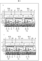
- FIG. 1A is a schematic plan view showing the configuration of the display device of the present embodiment
- FIG. 1B is a cross-sectional view showing the configuration of the display device.
- It is a circuit diagram which shows an example of a pixel circuit.
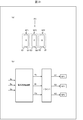
- FIG. 3A is a plan view showing the configuration of the pixels of the first embodiment
- FIG. 3B is a block diagram showing the configuration of the first embodiment.
- 4 (a) is a cross-sectional view taken along the line AA of FIG. 3 (a)
- FIG. 4 (b) is a cross-sectional view taken along the line BB of FIG. 3 (a).
- 5 (a) is a gradation brightness characteristic with respect to red
- FIG. 5 (b) is a voltage-luminance curve with respect to red
- FIG. 5 (c) is a gradation brightness characteristic with respect to blue.
- (D) is a voltage-luminance curve related to blue
- FIG. 5 (e) is a gradation brightness characteristic related to green
- FIG. 5 (f) is a voltage-luminance curve related to green.
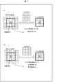
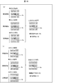
- FIG. 6A is a schematic diagram showing a method of processing a red input signal in the first control method
- FIG. 6B is a schematic diagram showing a method of processing a blue input signal in the first control method
- FIG. 6 (c) is a schematic diagram showing a method of processing a green input signal in the first control method. It is a schematic diagram which shows another processing method of the red input signal in the 1st control method.
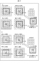
- FIG. 10A is a schematic diagram showing a method of processing a red input signal in the second control method
- FIG. 10B is a schematic diagram showing a method of processing a blue input signal in the second control method
- FIG. 10 (c) is a schematic diagram showing a method of processing a green input signal in the second control method
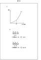
- FIG. 11A is a graph showing a color gamut of a light emitting element (OLED) having an organic light emitting layer and a color gamut of a light emitting element (QLED) having a quantum dot light emitting layer
- FIG. 11A is a graph showing a color gamut of a light emitting element (OLED) having an organic light emitting layer and a color gamut of a light emitting element (QLED) having a quantum dot light emitting layer
- FIG. 11A is a graph showing a color gamut of a light emitting element (OLED) having an organic light emitting layer and a color gamut of a light emitting element (QLED)
- FIG. 11B is a graph showing the th. 3 is a schematic diagram showing a method of processing a red input signal in the control method
- FIG. 11C is a schematic diagram showing a method of processing a blue input signal in the third control method
- FIG. 11 (d). ) Is a schematic diagram showing a method of processing a green input signal in the third control method.
- FIG. 12A is a schematic diagram showing a method of processing a red input signal in the fourth control method
- FIG. 12B is a schematic diagram showing a method of processing a blue input signal in the fourth control method.
- FIG. 12 (c) is a schematic diagram showing a method of processing a green input signal in the fourth control method.
- FIG. 12A is a schematic diagram showing a method of processing a red input signal in the fourth control method
- FIG. 12B is a schematic diagram showing a method of processing a blue input signal in the fourth control method
- FIG. 12 (c) is a schematic diagram showing a method of processing a
- FIG. 13A is a schematic diagram showing a method of processing a red input signal in the fifth control method
- FIG. 13B is a schematic diagram showing a method of processing a blue input signal in the fifth control method
- FIG. 13 (c) is a schematic diagram showing a method of processing a green input signal in the fifth control method
- FIG. 14A is a plan view showing the configuration of the pixels of the second embodiment
- FIG. 14B is a block diagram showing the configuration of the display device of the second embodiment.
- 15 (a) is a gradation brightness characteristic with respect to red
- FIG. 15 (b) is a voltage-luminance curve with respect to red
- FIG. 15 (c) is a gradation brightness characteristic with respect to blue.
- FIG. 15 (D) is a voltage-luminance curve for blue
- FIG. 15 (e) is a gradation brightness characteristic for green
- FIG. 15 (f) is a voltage-luminance curve for green.
- FIG. 18A is a gradation luminance characteristic with respect to white
- FIG. 18B is a schematic diagram showing a method of processing red, blue, and green input signals in the seventh control method.
- FIG. 18B is a schematic diagram showing a method of processing red, blue, and green input signals in the 8th control method.
- FIG. 21 (a) is a plan view showing the configuration of the pixels of the third embodiment
- FIG. 21 (b) is a block diagram showing the configuration of the display device of the third embodiment.
- FIG. 23A is a plan view showing the configuration of the pixels of the fourth embodiment
- FIG. 23B is a block diagram showing the configuration of the display device of the fourth embodiment.
- FIG. 24A is a plan view showing the configuration of the pixels of the fifth embodiment
- FIG. 24B is a block diagram showing the configuration of the display device of the fifth embodiment.
- FIG. 1A is a schematic plan view showing the configuration of the display device of the present embodiment
- FIG. 1B is a cross-sectional view showing the configuration of the display device.
- the barrier layer 3, the thin film transistor layer 4, the top emission (light emitting to the upper layer side) type light emitting element layer 5, and the sealing layer 6 are formed in this order on the substrate 12.
- a plurality of sub-pixel SPs, each including a self-luminous type light emitting element, are formed in the display area DA.
- a terminal portion TA is provided in the frame area NA surrounding the display area DA.
- the substrate 12 is a glass substrate or a flexible base material containing a resin such as polyimide as a main component.
- the substrate 12 can be composed of two layers of polyimide films and an inorganic film sandwiched between them. ..
- the barrier layer (undercoat layer) 3 is an inorganic insulating layer that prevents foreign substances such as water and oxygen from entering, and can be formed by using, for example, silicon nitride, silicon oxide, or the like.
- the thin film transistor layer 4 includes a semiconductor layer PS above the barrier layer 3, a gate insulating film 16 above the semiconductor layer PS, and a first layer above the gate insulating film 16.
- a metal layer including the gate electrode GE
- a first interlayer insulating film 18 above the first metal layer and a second metal layer above the first interlayer insulating film 18 (including the initialization wiring IL).
- the second interlayer insulating film 20 above the second metal layer, the third metal layer (including the data signal line DL) above the second interlayer insulating film 20, and the flattening of the upper layer than the third metal layer. Includes a film 21 and.
- the semiconductor layer PS is, for example, low-temperature polysilicon (LTPS), and the transistor TR is configured to include the gate electrode GE and the semiconductor layer PS.
- LTPS low-temperature polysilicon
- the first metal layer, the second metal layer, and the third metal layer are composed of, for example, a single-layer film or a multi-layer film of a metal containing at least one of aluminum, tungsten, molybdenum, tantalum, chromium, titanium, and copper. Will be done.
- the gate insulating film 16, the first interlayer insulating film 18, and the second interlayer insulating film 20 are composed of, for example, a silicon oxide (SiOx) film, a silicon nitride (SiNx) film, or a laminated film thereof formed by a CVD method. can do.
- the flattening film 21 can be made of a coatable organic material such as polyimide or acrylic resin.
- the light emitting element layer 5 includes a pixel electrode PE layer above the flattening film 21, an insulating edge cover film 23 covering the edge of the pixel electrode PE, and an EL (electroluminescence) layer 24 above the edge cover film 23.
- the upper electrode UE which is a layer above the EL layer 24.
- the edge cover film 23 is formed by applying an organic material such as polyimide or acrylic resin and then patterning by photolithography.
- each light emitting element has an island-shaped pixel electrode PE, an EL layer 24 (including a light emitting layer), and the like.
- the top electrode UE is a solid common electrode common to a plurality of light emitting elements.
- the EL layer 24 is composed of, for example, laminating a hole injection layer, a hole transport layer, a light emitting layer, an electron transport layer, and an electron injection layer in this order from the lower layer side.
- the light emitting layer is formed in an island shape at the opening (for each sub-pixel) of the edge cover film 23 by a vapor deposition method, an inkjet method, or a photolithography method.
- the other layers are formed in an island shape or a solid shape (common layer).
- the hole injection layer, the hole transport layer, the electron transport layer, and the electron injection layer may be configured so as not to form one or more layers.
- the pixel electrode PE (for example, the anode) is a light reflecting electrode composed of, for example, a laminate of ITO (Indium Tin Oxide) and an alloy containing Ag (silver) or Ag.
- the upper electrode UE (for example, the cathode) is made of a metal thin film such as a magnesium-silver alloy and has light transmission property.
- the light emitting element layer 5 contains a quantum dot light emitting layer containing quantum dots that emit light of primary colors (for example, red, blue, green) and an organic compound that emits light of primary colors (for example, red, blue, green).
- a light emitting layer is included.
- Quantum dots are, for example, inorganic semiconductors having a particle size of several nm to several tens of nm, and emit light by an electric current or the like.
- holes and electrons are recombined in the organic light emitting layer by the driving current between the pixel electrode PE and the upper electrode UE, and light is emitted in the process of transitioning the resulting excitons to the ground state. ..
- the quantum dot light emitting layer holes and electrons are recombined in the quantum dot light emitting layer by the driving current between the pixel electrode PE and the upper electrode UE, and the resulting excitons are the conduction band levels (conduction) of the quantum dots. Light is emitted in the process of transitioning from the band) to the valence band.
- the sealing layer 6 covering the light emitting element layer 5 is a layer that prevents foreign substances such as water and oxygen from penetrating into the light emitting element layer 5.
- the two-layer inorganic sealing film 26 can be composed of 28 and an organic film 27 formed between them.
- FIG. 2 is a circuit diagram showing an example of a pixel circuit.
- a light emitting element and a pixel circuit PK for controlling the light emitting element are provided for each sub-pixel, and the pixel circuit and wiring connected to the pixel circuit are formed in the thin film transistor layer 4.
- the capacitive element Cp, the first initialization transistor TR1 whose gate terminal is connected to the scanning signal line Gn-1 of the previous stage (n-1 stage), and the gate terminal are its own stage (n stage).
- the threshold control transistor TR2 connected to the scanning signal line Gn (first scanning signal line)
- the write control transistor TR3 whose gate terminal is connected to the scanning signal line Gn of its own stage (n stage)
- the light emitting element X Drive transistor TR4 that controls the current
- power supply transistor TR5 whose gate terminal is connected to the light emission control line EM (n stages)
- light emission control transistor TR6 whose gate terminal is connected to the light emission control line EM (n stages). And, including.
- the gate terminal of the drive transistor TR4 is connected to the high voltage side power supply line PL via the capacitive element Cp, and is also connected to the initialization power supply line IL via the first initialization transistor TR1.
- the source terminal of the drive transistor TR4 is connected to the data signal line DL via the write control transistor TR3, and is also connected to the high voltage side power supply line PL via the power supply transistor TR5.
- the drain terminal of the drive transistor TR4 is connected to the anode of the light emitting element X via the light emission control transistor TR6, and is also connected to the gate terminal of the drive transistor TR4 via the threshold control transistor TR2.
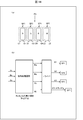
- FIG. 3A is a plan view showing the configuration of the pixels of the first embodiment
- FIG. 3B is a block diagram showing the configuration of the first embodiment
- 4 (a) is a cross-sectional view taken along the line AA of FIG. 3 (a)
- FIG. 4 (b) is a cross-sectional view taken along the line BB of FIG. 3 (a).
- the pixels of the first embodiment include a first pixel electrode E1 electrically connected to the first transistor TRa and a second pixel electrode E2 electrically connected to the second transistor TRb.
- the sixth pixel electrode E6 electrically connected to the sixth transistor TRf, the first light emitting layer Q1 formed above the first pixel electrode E1 and superposed on the first pixel electrode E1, and the second pixel electrode E2.
- the first pixel electrodes E1 to the sixth pixel electrodes E6 are formed in the same layer in an island shape.
- the upper layer means that the layer is formed in a process after the comparative layer, and the same layer means that the same material is formed in the same process.
- the first light emitting layer Q1 is a quantum dot light emitting layer that emits red (for example, the first color) light
- the second light emitting layer J2 is an organic light emitting layer that emits blue (for example, the second color) light.
- the third light emitting layer Q3 is a quantum dot light emitting layer that emits green (for example, a third color) light
- the fourth light emitting layer Q4 is a quantum dot light emitting layer that emits blue light, and is a fifth light emitting layer.
- J5 is an organic light emitting layer that emits red light
- the sixth light emitting layer J6 is an organic light emitting layer that emits green light. That is, each of the red, blue, and green lights is emitted from the quantum dot light emitting layer and the organic light emitting layer.
- the first sub-pixel SP1 includes a first pixel electrode E1 and a first light emitting layer Q1
- a second sub pixel SP2 includes a second pixel electrode E2 and a second light emitting layer J2
- a third sub pixel SP3 is a third subpixel SP3.
- the third pixel electrode E3 and the third light emitting layer Q3 are included
- the fourth sub pixel SP4 includes the fourth pixel electrode E4 and the fourth light emitting layer Q4
- the fifth sub pixel SP5 includes the fifth pixel electrode E5 and the fifth light emitting layer.
- the layer J5 is included
- the sixth sub-pixel SP6 includes a sixth pixel electrode E6 and a sixth light emitting layer J6.
- the pixel PX is arranged in the row direction (for example, the extending direction of the scanning signal line Gn), the first sub-pixel SP1, the third sub-pixel SP3, and the fourth sub-pixel SP4, and the first sub-pixel SP1 and the column direction (for example).
- FIG. 4 is a block diagram showing the configuration of the display device of the first embodiment.
- the display device 2 includes a signal processing circuit for processing an input signal and a driver for driving the pixel PX.
- the signal processing circuit receives an input signal (gradation data) for each color corresponding to each pixel and generates a signal (gradation data) corresponding to each sub-pixel.
- the first signal Rq and the second sub-pixel corresponding to the first sub-pixel SP1 are received by receiving the red input signal Rx, the blue input signal Bx, and the green input signal Gx corresponding to one pixel.
- the sixth signal Rj corresponding to the 6-subpixel SP6 is generated.
- 256 gradations (gradation value: 0 to 255) of each color will be described.
- the driver outputs the voltage signal A1 to the first sub-pixel SP1 based on the first signal Rq (digital signal), and outputs the voltage signal A2 to the second sub-pixel SP2 based on the second signal Bj (digital signal).
- the voltage signal A3 is output to the third sub-pixel SP3 based on the third signal Gq (digital signal), and the voltage signal A4 is output to the fourth sub-pixel SP4 based on the fourth signal Bq (digital signal).
- the voltage signal A5 is output to the 5th sub-pixel SP5 based on the 5 signal Gj (digital signal)
- the voltage signal A6 is output to the 6th sub-pixel SP6 based on the 6th signal Rj (digital signal).
- FIG. 5 (a) is a gradation brightness characteristic with respect to red
- FIG. 5 (b) is a voltage-luminance curve with respect to red
- FIG. 5 (c) is a gradation brightness characteristic with respect to blue
- (D) is a voltage-luminance curve related to blue
- FIG. 5 (e) is a gradation brightness characteristic related to green
- FIG. 5 (f) is a voltage-luminance curve related to green.
- the brightness L (Rx) corresponding to the red input signal Rx obtained from the red gradation brightness characteristic TLR is the first signal obtained from the red gradation brightness characteristic TLR. It is equal to the sum of the luminance L1 corresponding to Rq and the luminance L5 corresponding to the sixth signal Rj.
- the gradation luminance characteristic of the first sub-pixel and the gradation luminance characteristic of the sixth sub-pixel are each set to be the red gradation luminance characteristic TLR. In this way, the red gradation luminance characteristic TLR can be reproduced by emitting light only from the first sub-pixel or the sixth sub-pixel.
- the brightness L1 is a value corresponding to A1 in the voltage brightness curve VLRq of the first sub-pixel
- the brightness L6 is a value corresponding to A6 in the voltage brightness curve VLRj of the sixth sub-pixel.
- the luminance L (Bx) corresponding to the blue input signal Bx obtained from the blue gradation luminance characteristic TLB is the fourth signal obtained from the blue luminance characteristic TLB. It is equal to the sum of the luminance L4 corresponding to Bq and the luminance L2 corresponding to the second signal Bj.
- the gradation luminance characteristic of the second sub-pixel and the gradation luminance characteristic of the fourth sub-pixel are each set to be the blue gradation luminance characteristic TLB. In this way, the blue gradation luminance characteristic TLB can be reproduced by emitting light only from the second sub-pixel or the fourth sub-pixel.
- the brightness L4 is a value corresponding to A4 in the voltage brightness curve VLBq of the fourth sub-pixel
- the brightness L2 is a value corresponding to A2 in the voltage brightness curve VLBj of the second sub-pixel.
- the brightness L (Gx) corresponding to the green input signal Gx obtained from the green gradation brightness characteristic TLG is the third signal obtained from the green gradation brightness characteristic TLG. It is equal to the sum of the luminance L3 corresponding to Gq and the luminance L5 corresponding to the fifth signal Gj.
- the gradation luminance characteristic of the third sub-pixel and the gradation luminance characteristic of the fifth sub-pixel are each set to be the green gradation luminance characteristic TLG. In this way, the green gradation luminance characteristic TLG can be reproduced by emitting light only from the third sub-pixel or the fifth sub-pixel.
- the brightness L3 is a value corresponding to A3 in the voltage brightness curve VLGq of the third sub-pixel
- the brightness L5 is a value corresponding to A5 in the voltage brightness curve VLGj of the fifth sub-pixel.
- the brightness L (Rx) corresponding to the red input signal (Rx) can be calculated using the red gradation brightness characteristic TLR, and the red input corresponding to the brightness L (Rx) can be calculated using the inverse function.
- the blue gradation brightness characteristic TLB can be used to calculate the brightness L (Bx) corresponding to the blue input signal (Bx), and the inverse function can be used to correspond to the brightness L (Bx).
- the blue input signal Bx can be calculated.
- the brightness L (Bx) ⁇ L2 L4
- the fourth signal Bq can be calculated using an inverse function. ..
- the brightness L (Gx) corresponding to the green input signal (Gx) can be calculated using the green gradation brightness characteristic TLG
- the green corresponding to the brightness L (Gx) can be calculated using the inverse function.
- the input signal Gx of can be calculated.
- L5 is determined from the fifth signal Gj and the green gradation brightness characteristic TLG
- the brightness L (Gx) ⁇ L5 L3, so that the third signal Gq can be calculated using an inverse function. ..
- FIG. 6A is a schematic diagram showing a method of processing a red input signal in the first control method
- FIG. 6B is a schematic diagram showing a method of processing a blue input signal in the first control method
- FIG. 6 (c) is a schematic diagram showing a method of processing a green input signal in the first control method.
- the sixth signal Rj is the red gradation value average.
- the first signal Rq can be obtained by using the red gradation luminance characteristic TLR.
- the second signal Bj is the blue gradation value average.
- the blue input signal Bx of the pixel PX is smaller than the blue gradation value average, the second signal Rj is made equal to the blue input signal Bx.
- the fourth signal Bq can be obtained by using the blue gradation luminance characteristic TLB.
- the fifth signal Gj is the green gradation value average.
- the third signal Gq can be obtained by using the green gradation luminance characteristic TLG.
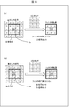
- FIG. 7 is a schematic diagram showing another processing method of the red input signal in the first control method.
- the image region including the pixel PX is filtered for the red input signal (for example, a two-dimensional low-pass filter LPF is applied), and the red input signal Rx of the pixel PX is the red of the pixel PX.
- the sixth signal Rj is equal to the red filter processing value when it is larger than the filter processing value of the pixel PX, and the red input signal of the pixel PX is equal to or less than the red filter processing value of the pixel PX.
- the 6 signal Rj is made equal to the red input signal Rx (the gradation value of the first signal Rq is set to 0).
- the first signal Rq can be obtained by using the red gradation luminance characteristic TLR.
- FIG. 8 is a schematic diagram showing another processing method of the blue input signal in the first control method.
- the image region including the pixel PX is filtered for the blue input signal (for example, a two-dimensional low-pass filter LPF is applied), and the blue input signal Bx of the pixel PX is the blue of the pixel PX.
- the second signal Bj is equal to the blue filter processing value when it is larger than the filter processing value of the pixel PX, and the red input signal of the pixel PX is equal to or less than the red filter processing value of the pixel PX.
- Make the 2 signal Bj equal to the blue input signal Bx (set the gradation value of the 4th signal Bq to 0).
- the fourth signal Bq can be obtained by using the blue gradation luminance characteristic TLB.
- FIG. 9 is a schematic diagram showing another processing method of the green input signal in the first control method.
- the image region including the pixel PX is filtered for the green input signal (for example, a two-dimensional low-pass filter LPF is applied), and the green input signal Gx of the pixel PX is the green of the pixel PX.
- the fifth signal Gj is equal to the green filter processing value
- the green input signal of the pixel PX is equal to or less than the green filter processing value of the pixel PX
- the fifth signal Gj is equal to or less than the green filter processing value.
- the third signal Gq can be obtained by using the green gradation luminance characteristic TLG.
- the first signal Rq, the fourth signal Bq, and the third signal Gq can be calculated based on the difference between the filtered value and the input signal.
- the first control method deterioration of the three-color organic light emitting layers (J2, J5, J6) can be suppressed, and a burn-in phenomenon caused by deterioration variation between pixels can be reduced.
- the light extraction efficiency of each of the quantum dot light emitting layer and the organic light emitting layer is enhanced.
- the size of the pixel area (block) is set to 3 pixels ⁇ 3 pixels, but it can be arbitrarily set such as 10 pixels ⁇ 10 pixels. Further, the number of taps of the LPFs shown in FIGS. 7 to 9 is only an example and can be set arbitrarily.
- FIG. 10A is a schematic diagram showing a method of processing a red input signal in the second control method
- FIG. 10B is a schematic diagram showing a method of processing a blue input signal in the second control method
- FIG. 10 (c) is a schematic diagram showing a method of processing a green input signal in the second control method.
- the gradation value of the red input signal Rx when the gradation value of the red input signal Rx is lower than the red threshold Rt, the gradation value of the first signal Rq is higher than the gradation value of the sixth signal Gj for the pixel PX.
- the gradation value Rq of the first signal when the red input signal Rx is higher than the red threshold Rt, the gradation value Rq of the first signal is made lower than the gradation value Rj of the fifth signal.
- the red threshold Rt> Rx 20
- the low gradation region (Q1, Q3, Q4) which is difficult to control the gradation with the three-color organic light emitting layer (J2, J5, J6), is displayed by the quantum dot light emitting layer (Q1, Q3, Q4), and the high gradation region.
- FIG. 11A is a graph showing a color gamut of a light emitting element (OLED) having an organic light emitting layer and a color gamut of a light emitting element (QLED) having a quantum dot light emitting layer
- FIG. 11B is a graph showing the th.
- 3 is a schematic diagram showing a method of processing a red input signal in the control method
- FIG. 11C is a schematic diagram showing a method of processing a blue input signal in the third control method
- FIG. 11 (d). ) Is a schematic diagram showing a method of processing a green input signal in the third control method.
- the display device 2 can utilize the color gamut of the light emitting element (OLED) having an organic light emitting layer and the color gamut of the light emitting element (QLED) having a quantum dot light emitting layer. can.
- OLED light emitting element
- QLED light emitting element
- the color is switched between the emission of the quantum dot light emitting layer (Q1, Q4, Q3) and the light emission of the organic light emitting layer (J2, J5, J6) according to the display color gamut mode. It is possible to adjust the reproduction range.
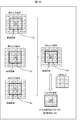
- FIG. 12A is a schematic diagram showing a method of processing a red input signal in the fourth control method
- FIG. 12B is a schematic diagram showing a method of processing a blue input signal in the fourth control method
- FIG. 12 (c) is a schematic diagram showing a method of processing a green input signal in the fourth control method.
- the image region including the pixel PX is filtered for the red input signal (for example, a two-dimensional low-pass filter LPF is applied), and the red input signal Rx of the pixel PX is the pixel.
- the first signal Rq can be obtained by using the red gradation luminance characteristic TLR.
- the image region including the pixel PX is filtered for the blue input signal (for example, a two-dimensional low-pass filter LPF is applied), and the blue input signal Bx of the pixel PX is the pixel.
- the fourth signal Bq can be obtained by using the blue gradation luminance characteristic TLB.
- the image region including the pixel PX is filtered for the green input signal (for example, a two-dimensional low-pass filter LPF is applied), and the green input signal Gx of the pixel PX is the pixel.
- the third signal Gq can be obtained by using the green gradation luminance characteristic TLG.
- the fourth control method in addition to suppressing deterioration of the organic light emitting layer at the time of peak luminance display, it is possible to improve color reproducibility by lighting the quantum dot light emitting layer.
- FIG. 13A is a schematic diagram showing a method of processing a red input signal in the fifth control method
- FIG. 13B is a schematic diagram showing a method of processing a blue input signal in the fifth control method
- FIG. 13 (c) is a schematic diagram showing a method of processing a green input signal in the fifth control method.
- One of the purposes of the fifth control method is to improve the quality of moving image display, and the hold type light emission of the organic light emitting layer and the impulse type light emission of the quantum dot light emitting layer are combined.
- the driver performs impulse control of the first sub-pixel SP1 based on the first signal Rq and hold control of the sixth sub-pixel SP6 based on the sixth signal Gj for the pixel PX.
- Rx 20 (Rx is a low gradation region)
- the driver performs impulse control of the fourth sub-pixel SP4 based on the fourth signal Bq and hold control of the second sub-pixel SP2 based on the second signal Bj for the pixel PX.
- the driver performs impulse control of the third sub-pixel SP3 based on the third signal Gq and hold control of the fifth sub-pixel SP5 based on the fifth signal Gj for the pixel PX.
- Gx 20 (Gx is a low gradation region)
- the impulse control of the quantum dot light emitting layer (Q1, Q4, Q3) and the hold control of the organic light emitting layer (J2, J6, J5) are performed according to the gradation values of the input signals of the three colors.
- FIG. 14A is a plan view showing the configuration of the pixels of the second embodiment
- FIG. 14B is a block diagram showing the configuration of the display device of the second embodiment.
- the first light emitting layer Q1 includes a quantum dot light emitting layer that emits red light
- the third light emitting layer Q3 includes a quantum dot light emitting layer that emits green light
- the fourth light emitting layer Q4. Includes a quantum dot light emitting layer that emits blue light
- a second light emitting layer J2 includes an organic light emitting layer that emits blue light
- a fifth light emitting layer J5 includes an organic light emitting layer that emits green light
- the sixth light emitting layer J6 includes an organic light emitting layer that emits red light.
- the first sub-pixel SP1 includes a first pixel electrode E1 and a first light emitting layer Q1
- a third sub pixel SP3 includes a third pixel electrode E3 and a third light emitting layer Q3
- a fourth sub pixel SP4 is a third.
- the 4-pixel electrode E4 and the fourth light emitting layer Q4 are included
- the seventh sub-pixel SP7 includes the second pixel electrode E2 and the second light emitting layer J2.
- the second light emitting layer J2 is a white light emitting layer formed above the second pixel electrode E2 and overlaps with the second pixel electrode E2.
- the second color light emitting layer J2 may be, for example, a white light emitting layer in which an organic light emitting layer that emits red light, an organic light emitting layer that emits blue light, and an organic light emitting layer that emits green light are laminated, or a red light emitting layer.
- a white light emitting layer may be a white light emitting layer in which an organic light emitting substance that emits light, an organic light emitting substance that emits blue light, and an organic light emitting substance that emits green light are mixed.
- the pixel PX is composed of a first sub-pixel SP1, a third sub-pixel SP3, a fourth sub-pixel SP4, and a seventh sub-pixel SP7 arranged in the row direction.
- the signal processing circuit receives the red input signal Rx, the blue input signal Bx, and the green input signal Gx, and receives the first signal Rq corresponding to the first sub-pixel SP1 and the third signal Rq corresponding to the third sub-pixel SP3.
- the signal Gq, the fourth signal Bq corresponding to the fourth sub-pixel SP4, and the seventh signal Wj corresponding to the seventh sub-pixel SP7 are generated.
- the minimum values of Rx, Bx, and Gx are Wx.
- the driver outputs the voltage signal A1 to the first sub-pixel SP1 based on the first signal Rq (digital signal), and outputs the voltage signal A3 to the third sub-pixel SP3 based on the third signal Gq (digital signal).
- the voltage signal A4 is output to the 4th sub-pixel SP4 based on the 4th signal Bq (digital signal), and the voltage signals A7r, A7b, A7g are output to the 7th sub-pixel SP7 based on the 7th signal Wj (digital signal). Output.
- FIG. 15 (a) is a gradation brightness characteristic with respect to red
- FIG. 15 (b) is a voltage-luminance curve with respect to red
- FIG. 15 (c) is a gradation brightness characteristic with respect to blue
- (D) is a voltage-luminance curve for blue
- FIG. 15 (e) is a gradation brightness characteristic for green
- FIG. 15 (f) is a voltage-luminance curve for green.
- the luminance L (Rx) corresponding to the red input signal Rx obtained from the red gradation luminance characteristic TLR is the first signal obtained from the red luminance characteristic TLR. It is equal to the sum of the luminance L1 corresponding to Rq and the luminance Lr corresponding to the seventh signal Wj.
- the brightness L1 is a value corresponding to A1 in the voltage brightness curve VLRq of the first sub-pixel
- the brightness Lr is a value corresponding to A7r in the voltage brightness curve VLRj of the red organic light emitting layer.
- the luminance L (Bx) corresponding to the blue input signal Bx obtained from the blue gradation luminance characteristic TLB is the fourth signal obtained from the blue luminance characteristic TLB. It is equal to the sum of the luminance L4 corresponding to Bq and the luminance Lb corresponding to the seventh signal Wj.
- the brightness L4 is a value corresponding to A4 in the voltage brightness curve VLBq of the fourth sub-pixel
- the brightness Lb is a value corresponding to A7b in the voltage brightness curve VLBj of the blue organic light emitting layer.
- the brightness L (Gx) corresponding to the green input signal Gx obtained from the green gradation brightness characteristic TLG is the third signal obtained from the green gradation brightness characteristic TLG. It is equal to the sum of the luminance L3 corresponding to Gq and the luminance Lg corresponding to the seventh signal Wj.
- the brightness L3 is a value corresponding to A3 in the voltage brightness curve VLGq of the third sub-pixel
- the brightness Lg is a value corresponding to A7g in the voltage brightness curve VLGj of the green organic light emitting layer.
- FIG. 16 is a schematic diagram showing a method of processing red, blue, and green input signals in the sixth control method.
- the seventh signal Wj is made equal to the white gradation value average.
- the seventh signal Wj is made equal to the white input signal Wx.
- the seventh signal Wj 30.
- the first signal Rq, the fourth signal Bq, and the third signal Gq can be obtained by using the gradation luminance characteristics TLR, TLB, and TLG (see FIG. 15).
- FIG. 17 is a schematic diagram showing another processing method of the red, blue, and green input signals in the sixth control method.
- the image region including the pixel PX is filtered for the white input signal Wx, and when the white input signal Wx of the pixel PX is larger than the white filtered value of the pixel PX,
- the 7th signal Wj is equal to the white filter processing value and the white input signal Wx of the pixel PX is equal to or less than the white filter processing value of the pixel PX
- the 7th signal Wj is referred to as the white input signal Wx. Make it equal.
- the first signal Rq, the fourth signal Bq, and the third signal Gq can be obtained by using the gradation luminance characteristics TLR, TLB, and TLG (see FIG. 15).
- the deterioration of the organic light emitting layer of the seventh sub-pixel SP7 can be suppressed, and the burn-in phenomenon caused by the deterioration variation between the pixels can be reduced.
- the size of the pixel area (block) and the number of taps of the LPF are set to 3 pixels ⁇ 3 pixels, but can be arbitrarily set such as 10 pixels ⁇ 10 pixels.
- FIG. 18A is a gradation luminance characteristic with respect to white
- FIG. 18B is a schematic diagram showing a method of processing red, blue, and green input signals in the seventh control method.
- the gradation value of the seventh signal Wj is set to zero, and the white input signal Wx of the pixel PX is set to zero.
- the seventh signal Wj is made equal to the white input signal Wx.
- the first signal Rq, the fourth signal Bq, and the third signal Gq can be obtained by using the gradation luminance characteristics TLR, TLB, and TLG (see FIG. 15).
- the low gradation region (Q1, Q3, Q4) which is difficult to control the gradation with the three-color organic light emitting layer (J2, J5, J6), is displayed by the quantum dot light emitting layer (Q1, Q3, Q4), and the high gradation region.
- FIG. 19 is a schematic diagram showing a method of processing red, blue, and green input signals in the eighth control method.
- the image region including the pixel PX is filtered for the white input signal (for example, the application of the two-dimensional low-pass filter LPF), and the white input signal Wx of the pixel PX is the white of the pixel PX.
- the 7th signal Wj is made equal to the filtered value of white.
- the first signal Rq, the fourth signal Bq, and the third signal Gq can be obtained by using the gradation luminance characteristics TLR, TLB, and TLG (see FIG. 15).
- the eighth control method in addition to suppressing deterioration of the organic light emitting layer at the time of peak luminance display, power consumption is suppressed by lighting the organic light emitting layer, and color reproducibility is improved by lighting the quantum dot light emitting layer. Can be planned.
- FIG. 20 is a schematic diagram showing a method of processing red, blue, and green input signals in the ninth control method.
- the driver performs impulse control based on the first signal Rq, the fourth signal Bq, and the third signal Gq and hold control based on the seventh signal Wj for the pixel PX.
- the first signal Rq 190
- the fourth signal Bq 190
- the brightness corresponding to Rx of the gradation brightness characteristic TLR (brightness corresponding to Rq of the gradation brightness characteristic TLR) ⁇ 1/3 + the brightness corresponding to Wj of the gradation brightness characteristic TLR, the gradation brightness characteristic TLB.
- Luminance corresponding to Bx (luminance corresponding to Bq of gradation brightness characteristic TLB) ⁇ 1/3 + brightness corresponding to Wj of gradation brightness characteristic TLB
- brightness corresponding to Gx of gradation brightness characteristic TLG (gradation)
- the relationship is (brightness corresponding to Gq of the luminance characteristic TLG) ⁇ 1/3 + luminance corresponding to Wj of the gradation luminance characteristic TLG.
- the impulse control of the quantum dot light emitting layer (Q1, Q4, Q3) and the hold control of the organic light emitting layer (J2, J6, J5) are performed according to the gradation values of the input signals of the three colors.
- FIG. 21 (a) is a plan view showing the configuration of the pixels of the third embodiment
- FIG. 21 (b) is a block diagram showing the configuration of the display device of the third embodiment.
- the first light emitting layer Q1 includes a quantum dot light emitting layer that emits red (for example, red)
- the second light emitting layer J2 includes an organic light emitting layer that emits blue (for example, blue).
- the third light emitting layer Q3 includes a quantum dot light emitting layer that emits green (for example, green).
- the first sub-pixel SP1 includes a first pixel electrode E1 and a first light emitting layer Q1
- the second sub pixel SP2 includes a second pixel electrode E2 and a second light emitting layer J2
- the third sub pixel SP3 is a third subpixel SP3.
- the pixel PX is composed of a first sub-pixel SP1, a third sub-pixel SP3, and a second sub-pixel SP2 arranged in the row direction.
- the signal processing circuit receives the red input signal Rx, the blue input signal Bx, and the green input signal Gx, and receives the first signal Rq corresponding to the first sub-pixel SP1 and the second signal Rq corresponding to the second sub-pixel SP2.
- a third signal Gq corresponding to the signal Bj and the third sub-pixel SP3 is generated.
- FIG. 22 is a schematic diagram showing a method of processing red, blue, and green input signals in the tenth control method.
- the driver performs impulse control based on the first signal Rq and the third signal Gq and hold control based on the second signal Bj for the pixel PX.
- the first signal Rq 60, th.
- the moving image is obtained by performing impulse control of the quantum dot light emitting layer (Q1 and Q3) and hold control of the organic light emitting layer (J2) according to the gradation values of the input signals of the three colors.
- the quantum dot light emitting layer Q1 and Q3
- hold control of the organic light emitting layer J2
- FIG. 23A is a plan view showing the configuration of the pixels of the fourth embodiment
- FIG. 23B is a block diagram showing the configuration of the display device of the fourth embodiment.
- the first light emitting layer Q1 includes a quantum dot light emitting layer that emits red light
- the second light emitting layer J2 includes an organic light emitting layer that emits blue light
- the third light emitting layer Q3 The fifth light emitting layer J5 includes an organic light emitting layer that emits green light.
- the first sub-pixel SP1 includes a first pixel electrode E1 and a first light emitting layer Q1
- the second sub pixel SP2 includes a second pixel electrode E2 and a second light emitting layer J2
- the third sub pixel SP3 is a third subpixel SP3.
- the three-pixel electrode E3 and the third light emitting layer Q3 are included
- the fifth sub-pixel SP5 includes the fifth pixel electrode E5 and the fifth light emitting layer J5.
- the pixel PX is composed of a first sub-pixel SP1, a third sub-pixel SP3, a fifth sub-pixel SP5, and a second sub-pixel SP2 arranged in the row direction.
- the signal processing circuit receives the red input signal Rx, the blue input signal Bx, and the green input signal Gx, and receives the first signal Rq corresponding to the first sub-pixel SP1 and the second signal Rq corresponding to the second sub-pixel SP2.
- the signal Bj, the third signal Gq corresponding to the third sub-pixel SP3, and the fifth signal Gj corresponding to the fifth sub-pixel SP5 are generated.
- the first control method, the second control method, the third control method, the fourth control method, and the fifth control method described in the first embodiment can be performed.
- control method of FIG. 10C can be applied to the third signal Gq corresponding to the third sub-pixel SP3 and the fifth signal Gj corresponding to the fifth sub-pixel SP5.
- control method of FIG. 11D can be applied to the third signal Gq corresponding to the third sub-pixel SP3 and the fifth signal Gj corresponding to the fifth sub-pixel SP5.
- control method of FIG. 12C can be applied to the third signal Gq corresponding to the third sub-pixel SP3 and the fifth signal Gj corresponding to the fifth sub-pixel SP5.
- control method of FIG. 13C can be applied to the third signal Gq corresponding to the third sub-pixel SP3 and the fifth signal Gj corresponding to the fifth sub-pixel SP5.
- FIG. 24A is a plan view showing the configuration of the pixels of the fifth embodiment
- FIG. 24B is a block diagram showing the configuration of the display device of the fifth embodiment.
- the first light emitting layer Q1 includes a quantum dot light emitting layer that emits red light
- the second light emitting layer J2 includes an organic light emitting layer that emits blue light
- the third light emitting layer Q3 A quantum dot light emitting layer that emits green light is included
- the fourth light emitting layer Q4 includes a quantum dot light emitting layer that emits blue light.
- the first sub-pixel SP1 includes a first pixel electrode E1 and a first light emitting layer Q1
- the second sub pixel SP2 includes a second pixel electrode E2 and a second light emitting layer J2
- the third sub pixel SP3 is a third subpixel SP3.
- the three-pixel electrode E3 and the third light emitting layer Q3 are included
- the fourth sub-pixel SP4 includes the fourth pixel electrode E4 and the fourth light emitting layer Q4.
- the pixel PX is arranged in the row direction, the first sub-pixel SP1 and the fourth sub-pixel SP4, the second sub-pixel SP2 adjacent to the first sub-pixel SP1 in the column direction, and the fourth sub-pixel SP4 adjacent to the fourth sub-pixel SP4 in the column direction. It is composed of a third sub-pixel SP3.
- the signal processing circuit receives the red input signal Rx, the blue input signal Bx, and the green input signal Gx, and receives the first signal Rq corresponding to the first sub-pixel SP1 and the second signal Rq corresponding to the second sub-pixel SP2.
- the signal Bj, the third signal Gq corresponding to the third sub-pixel SP3, and the fourth signal Bq corresponding to the fourth sub-pixel SP4 are generated.
- the first control method, the second control method, the third control method, the fourth control method, and the fifth control method described in the first embodiment can be performed.
- control methods of FIGS. 6B and 8 can be applied to the second signal Bj corresponding to the second sub-pixel SP2 and the fourth signal Bq corresponding to the fourth sub-pixel SP4.
- control method of FIG. 10B can be applied to the second signal Bj corresponding to the second sub-pixel SP2 and the fourth signal Bq corresponding to the fourth sub-pixel SP4.
- control method of FIG. 11C can be applied to the second signal Bj corresponding to the second sub-pixel SP2 and the fourth signal Bq corresponding to the fourth sub-pixel SP4.
- control method of FIG. 12B can be applied to the second signal Bj corresponding to the second sub-pixel SP2 and the fourth signal Bq corresponding to the fourth sub-pixel SP4.
- control method of FIG. 13B can be applied to the second signal Bj corresponding to the second sub-pixel SP2 and the fourth signal Bq corresponding to the fourth sub-pixel SP4.
- Display device 4 Thin film transistor layer 5 Light emitting element layer 6 Sealing layer 12 Substrate 16 Gate insulating film 18 First interlayer insulating film 20 Second interlayer insulating film 21 Flattening film 22 First electrode 23 Edge cover film 24 EL layer 25 Second Electrode X light emitting element SP1 to SP6 1st to 6th sub-pixels E1 to E6 1st to 6th pixel Electrodes Q1, Q3, Q4 Quantum dot light emitting layer J2, J5, J6 Organic light emitting layer
Landscapes
- Engineering & Computer Science (AREA)
- Physics & Mathematics (AREA)
- General Physics & Mathematics (AREA)
- Theoretical Computer Science (AREA)
- Computer Hardware Design (AREA)
- Crystallography & Structural Chemistry (AREA)
- Chemical & Material Sciences (AREA)
- Inorganic Chemistry (AREA)
- Nanotechnology (AREA)
- Optics & Photonics (AREA)
- Electroluminescent Light Sources (AREA)
- Control Of Indicators Other Than Cathode Ray Tubes (AREA)
- Control Of El Displays (AREA)
- Devices For Indicating Variable Information By Combining Individual Elements (AREA)
Priority Applications (5)
| Application Number | Priority Date | Filing Date | Title |
|---|---|---|---|
| JP2021573645A JP7329080B2 (ja) | 2020-01-27 | 2020-01-27 | 表示装置 |
| PCT/JP2020/002821 WO2021152672A1 (ja) | 2020-01-27 | 2020-01-27 | 表示装置 |
| US17/794,600 US11804182B2 (en) | 2020-01-27 | 2020-01-27 | Display device with pixel structure capable of extracting light from quantum-dot light-emitting layer and organic light-emitting layer of pixel structure |
| JP2023127424A JP7482299B2 (ja) | 2020-01-27 | 2023-08-04 | 表示装置 |
| US18/244,914 US12165595B2 (en) | 2020-01-27 | 2023-09-12 | Display device with enhanced light extraction efficiency |
Applications Claiming Priority (1)
| Application Number | Priority Date | Filing Date | Title |
|---|---|---|---|
| PCT/JP2020/002821 WO2021152672A1 (ja) | 2020-01-27 | 2020-01-27 | 表示装置 |
Related Child Applications (2)
| Application Number | Title | Priority Date | Filing Date |
|---|---|---|---|
| US17/794,600 A-371-Of-International US11804182B2 (en) | 2020-01-27 | 2020-01-27 | Display device with pixel structure capable of extracting light from quantum-dot light-emitting layer and organic light-emitting layer of pixel structure |
| US18/244,914 Continuation US12165595B2 (en) | 2020-01-27 | 2023-09-12 | Display device with enhanced light extraction efficiency |
Publications (1)
| Publication Number | Publication Date |
|---|---|
| WO2021152672A1 true WO2021152672A1 (ja) | 2021-08-05 |
Family
ID=77079582
Family Applications (1)
| Application Number | Title | Priority Date | Filing Date |
|---|---|---|---|
| PCT/JP2020/002821 Ceased WO2021152672A1 (ja) | 2020-01-27 | 2020-01-27 | 表示装置 |
Country Status (3)
| Country | Link |
|---|---|
| US (2) | US11804182B2 (https=) |
| JP (2) | JP7329080B2 (https=) |
| WO (1) | WO2021152672A1 (https=) |
Cited By (1)
| Publication number | Priority date | Publication date | Assignee | Title |
|---|---|---|---|---|
| WO2024142375A1 (ja) * | 2022-12-28 | 2024-07-04 | シャープディスプレイテクノロジー株式会社 | 制御装置、表示装置及び表示パネルの制御方法 |
Families Citing this family (2)
| Publication number | Priority date | Publication date | Assignee | Title |
|---|---|---|---|---|
| KR20230049187A (ko) * | 2021-10-05 | 2023-04-13 | 삼성디스플레이 주식회사 | 표시 장치 및 그의 열화 보상 방법 |
| WO2023100244A1 (ja) * | 2021-11-30 | 2023-06-08 | シャープディスプレイテクノロジー株式会社 | 表示装置 |
Citations (15)
| Publication number | Priority date | Publication date | Assignee | Title |
|---|---|---|---|---|
| JP2006215559A (ja) * | 2005-02-03 | 2006-08-17 | Toppoly Optoelectronics Corp | 有機発光ディスプレイ装置およびその画像を表示する方法 |
| JP2007122033A (ja) * | 2005-09-30 | 2007-05-17 | Semiconductor Energy Lab Co Ltd | 表示装置及び電子機器 |
| US20090128458A1 (en) * | 2007-11-16 | 2009-05-21 | Hyo-Seok Kim | Organic light emitting diode display |
| US20090261715A1 (en) * | 2008-04-22 | 2009-10-22 | Un-Cheol Sung | Organic light emitting display device |
| US20130175514A1 (en) * | 2012-01-09 | 2013-07-11 | Samsung Display Co., Ltd. | Display device |
| US20160248029A1 (en) * | 2014-07-09 | 2016-08-25 | Shenzhen China Star Optoelectronics Technology Co., Ltd. | Oled pixel structure |
| CN105932028A (zh) * | 2016-06-07 | 2016-09-07 | 深圳市华星光电技术有限公司 | 自发光显示装置 |
| CN106601923A (zh) * | 2016-12-19 | 2017-04-26 | 华南理工大学 | 一种有机、无机量子点杂化的全彩显示器件及其制备方法 |
| CN107527942A (zh) * | 2017-09-05 | 2017-12-29 | 上海天马有机发光显示技术有限公司 | 有机发光显示面板及其制备方法 |
| CN107611274A (zh) * | 2017-09-05 | 2018-01-19 | 上海天马有机发光显示技术有限公司 | 有机发光显示面板及有机发光显示装置 |
| US20180108872A1 (en) * | 2016-05-03 | 2018-04-19 | Shenzhen China Star Optoelectronics Technology Co., Ltd. | Self-luminous display device and manufacturing method thereof |
| US20180130853A1 (en) * | 2014-12-11 | 2018-05-10 | Guanzhou Chinaray Optoelectronic Materials Ltd. | Display component and manufacturing method therefor |
| US20180261783A1 (en) * | 2017-03-09 | 2018-09-13 | Samsung Display Co., Ltd. | Light emitting display device |
| CN109473560A (zh) * | 2018-11-19 | 2019-03-15 | 京东方科技集团股份有限公司 | 显示面板及其制造方法、车载显示装置 |
| CN109616504A (zh) * | 2018-12-12 | 2019-04-12 | 惠科股份有限公司 | 显示面板 |
Family Cites Families (9)
| Publication number | Priority date | Publication date | Assignee | Title |
|---|---|---|---|---|
| EP1770676B1 (en) | 2005-09-30 | 2017-05-03 | Semiconductor Energy Laboratory Co., Ltd. | Display device and electronic device |
| TWI559525B (zh) * | 2012-12-27 | 2016-11-21 | Lg顯示器股份有限公司 | 有機發光二極體顯示裝置及其製造方法 |
| JP2015216059A (ja) | 2014-05-12 | 2015-12-03 | 株式会社ジャパンディスプレイ | 発光素子表示装置 |
| CN104253247A (zh) | 2014-10-13 | 2014-12-31 | 深圳市华星光电技术有限公司 | Oled器件的制备方法及其制得的oled器件 |
| US10192932B2 (en) * | 2016-02-02 | 2019-01-29 | Apple Inc. | Quantum dot LED and OLED integration for high efficiency displays |
| US10467952B2 (en) | 2016-10-12 | 2019-11-05 | Shaoher Pan | Integrated light-emitting diode arrays for displays |
| GB201806530D0 (en) | 2018-04-21 | 2018-06-06 | Savvy Science Ltd | Pixel arrangement comprising a perovskite light emitting diode |
| US11264582B2 (en) * | 2019-03-03 | 2022-03-01 | Innolux Corporation | Light emitting device |
| CN110797376A (zh) * | 2019-10-10 | 2020-02-14 | 复旦大学 | 一种双面显示装置 |
-
2020
- 2020-01-27 WO PCT/JP2020/002821 patent/WO2021152672A1/ja not_active Ceased
- 2020-01-27 JP JP2021573645A patent/JP7329080B2/ja active Active
- 2020-01-27 US US17/794,600 patent/US11804182B2/en active Active
-
2023
- 2023-08-04 JP JP2023127424A patent/JP7482299B2/ja active Active
- 2023-09-12 US US18/244,914 patent/US12165595B2/en active Active
Patent Citations (15)
| Publication number | Priority date | Publication date | Assignee | Title |
|---|---|---|---|---|
| JP2006215559A (ja) * | 2005-02-03 | 2006-08-17 | Toppoly Optoelectronics Corp | 有機発光ディスプレイ装置およびその画像を表示する方法 |
| JP2007122033A (ja) * | 2005-09-30 | 2007-05-17 | Semiconductor Energy Lab Co Ltd | 表示装置及び電子機器 |
| US20090128458A1 (en) * | 2007-11-16 | 2009-05-21 | Hyo-Seok Kim | Organic light emitting diode display |
| US20090261715A1 (en) * | 2008-04-22 | 2009-10-22 | Un-Cheol Sung | Organic light emitting display device |
| US20130175514A1 (en) * | 2012-01-09 | 2013-07-11 | Samsung Display Co., Ltd. | Display device |
| US20160248029A1 (en) * | 2014-07-09 | 2016-08-25 | Shenzhen China Star Optoelectronics Technology Co., Ltd. | Oled pixel structure |
| US20180130853A1 (en) * | 2014-12-11 | 2018-05-10 | Guanzhou Chinaray Optoelectronic Materials Ltd. | Display component and manufacturing method therefor |
| US20180108872A1 (en) * | 2016-05-03 | 2018-04-19 | Shenzhen China Star Optoelectronics Technology Co., Ltd. | Self-luminous display device and manufacturing method thereof |
| CN105932028A (zh) * | 2016-06-07 | 2016-09-07 | 深圳市华星光电技术有限公司 | 自发光显示装置 |
| CN106601923A (zh) * | 2016-12-19 | 2017-04-26 | 华南理工大学 | 一种有机、无机量子点杂化的全彩显示器件及其制备方法 |
| US20180261783A1 (en) * | 2017-03-09 | 2018-09-13 | Samsung Display Co., Ltd. | Light emitting display device |
| CN107611274A (zh) * | 2017-09-05 | 2018-01-19 | 上海天马有机发光显示技术有限公司 | 有机发光显示面板及有机发光显示装置 |
| CN107527942A (zh) * | 2017-09-05 | 2017-12-29 | 上海天马有机发光显示技术有限公司 | 有机发光显示面板及其制备方法 |
| CN109473560A (zh) * | 2018-11-19 | 2019-03-15 | 京东方科技集团股份有限公司 | 显示面板及其制造方法、车载显示装置 |
| CN109616504A (zh) * | 2018-12-12 | 2019-04-12 | 惠科股份有限公司 | 显示面板 |
Cited By (1)
| Publication number | Priority date | Publication date | Assignee | Title |
|---|---|---|---|---|
| WO2024142375A1 (ja) * | 2022-12-28 | 2024-07-04 | シャープディスプレイテクノロジー株式会社 | 制御装置、表示装置及び表示パネルの制御方法 |
Also Published As
| Publication number | Publication date |
|---|---|
| JPWO2021152672A1 (https=) | 2021-08-05 |
| US11804182B2 (en) | 2023-10-31 |
| JP7482299B2 (ja) | 2024-05-13 |
| JP7329080B2 (ja) | 2023-08-17 |
| US20230063949A1 (en) | 2023-03-02 |
| US12165595B2 (en) | 2024-12-10 |
| US20230419909A1 (en) | 2023-12-28 |
| JP2023153948A (ja) | 2023-10-18 |
Similar Documents
| Publication | Publication Date | Title |
|---|---|---|
| US11233097B2 (en) | Display device including dummy pixels with transmissive areas | |
| JP7482299B2 (ja) | 表示装置 | |
| US10056447B2 (en) | Organic light emitting display device | |
| KR102769670B1 (ko) | 유기 발광 표시 장치 | |
| JP6219656B2 (ja) | 有機el表示装置 | |
| KR102607376B1 (ko) | 유기 발광 표시 장치 | |
| TW201724496A (zh) | 有機發光二極體顯示器 | |
| CN104134678A (zh) | 有机发光二极管显示器 | |
| KR20120134222A (ko) | 백색 유기발광다이오드 표시소자 | |
| KR20200141548A (ko) | 유기 발광 표시 장치 | |
| KR20160082760A (ko) | 양자점을 포함하는 유기발광 다이오드 표시장치 | |
| CN112750880B (zh) | 有机发光显示设备 | |
| JP6749160B2 (ja) | 表示装置 | |
| KR20160134918A (ko) | 유기 발광 표시 장치 | |
| WO2016132954A1 (ja) | エレクトロルミネッセンス装置 | |
| CN111164500B (zh) | 显示设备 | |
| KR102907888B1 (ko) | 표시 장치 | |
| WO2020026307A1 (ja) | 表示デバイス | |
| CN113053951B (zh) | 包括白色有机发光器件的显示装置 | |
| KR102930220B1 (ko) | 표시 장치 | |
| KR20150079127A (ko) | 유기 발광 표시 장치 | |
| JP7312697B2 (ja) | 表示装置および電子機器 | |
| KR20250000921A (ko) | 표시 장치 | |
| CN113711291B (zh) | 显示装置 | |
| KR102742495B1 (ko) | 표시장치 |
Legal Events
| Date | Code | Title | Description |
|---|---|---|---|
| 121 | Ep: the epo has been informed by wipo that ep was designated in this application |
Ref document number: 20916593 Country of ref document: EP Kind code of ref document: A1 |
|
| ENP | Entry into the national phase |
Ref document number: 2021573645 Country of ref document: JP Kind code of ref document: A |
|
| NENP | Non-entry into the national phase |
Ref country code: DE |
|
| 122 | Ep: pct application non-entry in european phase |
Ref document number: 20916593 Country of ref document: EP Kind code of ref document: A1 |