WO2021152655A1 - Plasma treatment device - Google Patents
Plasma treatment device Download PDFInfo
- Publication number
- WO2021152655A1 WO2021152655A1 PCT/JP2020/002737 JP2020002737W WO2021152655A1 WO 2021152655 A1 WO2021152655 A1 WO 2021152655A1 JP 2020002737 W JP2020002737 W JP 2020002737W WO 2021152655 A1 WO2021152655 A1 WO 2021152655A1
- Authority
- WO
- WIPO (PCT)
- Prior art keywords
- waveguide
- plasma
- plasma processing
- processing apparatus
- circular waveguide
- Prior art date
Links
Images


Classifications
-
- H—ELECTRICITY
- H01—ELECTRIC ELEMENTS
- H01J—ELECTRIC DISCHARGE TUBES OR DISCHARGE LAMPS
- H01J37/00—Discharge tubes with provision for introducing objects or material to be exposed to the discharge, e.g. for the purpose of examination or processing thereof
- H01J37/32—Gas-filled discharge tubes
- H01J37/32009—Arrangements for generation of plasma specially adapted for examination or treatment of objects, e.g. plasma sources
- H01J37/32192—Microwave generated discharge
- H01J37/32311—Circuits specially adapted for controlling the microwave discharge
-
- H—ELECTRICITY
- H01—ELECTRIC ELEMENTS
- H01J—ELECTRIC DISCHARGE TUBES OR DISCHARGE LAMPS
- H01J37/00—Discharge tubes with provision for introducing objects or material to be exposed to the discharge, e.g. for the purpose of examination or processing thereof
- H01J37/32—Gas-filled discharge tubes
- H01J37/32009—Arrangements for generation of plasma specially adapted for examination or treatment of objects, e.g. plasma sources
- H01J37/32192—Microwave generated discharge
- H01J37/32211—Means for coupling power to the plasma
- H01J37/3222—Antennas
-
- H—ELECTRICITY
- H01—ELECTRIC ELEMENTS
- H01J—ELECTRIC DISCHARGE TUBES OR DISCHARGE LAMPS
- H01J37/00—Discharge tubes with provision for introducing objects or material to be exposed to the discharge, e.g. for the purpose of examination or processing thereof
- H01J37/32—Gas-filled discharge tubes
- H01J37/32009—Arrangements for generation of plasma specially adapted for examination or treatment of objects, e.g. plasma sources
- H01J37/32192—Microwave generated discharge
- H01J37/32211—Means for coupling power to the plasma
- H01J37/32229—Waveguides
-
- H—ELECTRICITY
- H01—ELECTRIC ELEMENTS
- H01J—ELECTRIC DISCHARGE TUBES OR DISCHARGE LAMPS
- H01J37/00—Discharge tubes with provision for introducing objects or material to be exposed to the discharge, e.g. for the purpose of examination or processing thereof
- H01J37/32—Gas-filled discharge tubes
- H01J37/32009—Arrangements for generation of plasma specially adapted for examination or treatment of objects, e.g. plasma sources
- H01J37/32192—Microwave generated discharge
- H01J37/32266—Means for controlling power transmitted to the plasma
-
- H—ELECTRICITY
- H01—ELECTRIC ELEMENTS
- H01J—ELECTRIC DISCHARGE TUBES OR DISCHARGE LAMPS
- H01J37/00—Discharge tubes with provision for introducing objects or material to be exposed to the discharge, e.g. for the purpose of examination or processing thereof
- H01J37/32—Gas-filled discharge tubes
- H01J37/32431—Constructional details of the reactor
- H01J37/3266—Magnetic control means
- H01J37/32669—Particular magnets or magnet arrangements for controlling the discharge
-
- H—ELECTRICITY
- H01—ELECTRIC ELEMENTS
- H01J—ELECTRIC DISCHARGE TUBES OR DISCHARGE LAMPS
- H01J37/00—Discharge tubes with provision for introducing objects or material to be exposed to the discharge, e.g. for the purpose of examination or processing thereof
- H01J37/32—Gas-filled discharge tubes
- H01J37/32431—Constructional details of the reactor
- H01J37/3266—Magnetic control means
- H01J37/32678—Electron cyclotron resonance
-
- H—ELECTRICITY
- H01—ELECTRIC ELEMENTS
- H01L—SEMICONDUCTOR DEVICES NOT COVERED BY CLASS H10
- H01L21/00—Processes or apparatus adapted for the manufacture or treatment of semiconductor or solid state devices or of parts thereof
- H01L21/02—Manufacture or treatment of semiconductor devices or of parts thereof
- H01L21/04—Manufacture or treatment of semiconductor devices or of parts thereof the devices having at least one potential-jump barrier or surface barrier, e.g. PN junction, depletion layer or carrier concentration layer
- H01L21/18—Manufacture or treatment of semiconductor devices or of parts thereof the devices having at least one potential-jump barrier or surface barrier, e.g. PN junction, depletion layer or carrier concentration layer the devices having semiconductor bodies comprising elements of Group IV of the Periodic System or AIIIBV compounds with or without impurities, e.g. doping materials
- H01L21/30—Treatment of semiconductor bodies using processes or apparatus not provided for in groups H01L21/20 - H01L21/26
- H01L21/302—Treatment of semiconductor bodies using processes or apparatus not provided for in groups H01L21/20 - H01L21/26 to change their surface-physical characteristics or shape, e.g. etching, polishing, cutting
- H01L21/306—Chemical or electrical treatment, e.g. electrolytic etching
- H01L21/3065—Plasma etching; Reactive-ion etching
-
- H—ELECTRICITY
- H01—ELECTRIC ELEMENTS
- H01P—WAVEGUIDES; RESONATORS, LINES, OR OTHER DEVICES OF THE WAVEGUIDE TYPE
- H01P3/00—Waveguides; Transmission lines of the waveguide type
- H01P3/16—Dielectric waveguides, i.e. without a longitudinal conductor
-
- H—ELECTRICITY
- H01—ELECTRIC ELEMENTS
- H01J—ELECTRIC DISCHARGE TUBES OR DISCHARGE LAMPS
- H01J2237/00—Discharge tubes exposing object to beam, e.g. for analysis treatment, etching, imaging
- H01J2237/32—Processing objects by plasma generation
- H01J2237/33—Processing objects by plasma generation characterised by the type of processing
- H01J2237/334—Etching
- H01J2237/3341—Reactive etching
Definitions
- the present invention relates to a plasma processing apparatus that generates plasma by electromagnetic waves.
- Plasma processing equipment is used in the production of semiconductor integrated circuit elements.
- a plasma processing device that generates plasma by electromagnetic waves a device in which a static magnetic field is applied to a plasma processing chamber is widely used. This is because the static magnetic field has the advantage that the plasma loss can be suppressed and the plasma distribution can be controlled. Furthermore, by using the interaction between electromagnetic waves and static magnetic fields, there is an effect that plasma can be generated even under operating conditions where it is usually difficult to generate plasma.
- RF bias technology is used to speed up plasma processing and improve processing quality by applying high frequencies to the substrate to be processed during plasma processing and drawing ions in the plasma to the surface of the substrate to be processed.
- plasma etching processing since ions are vertically incident on the surface to be processed of the substrate to be processed, anisotropic processing in which etching proceeds only in the vertical direction of the substrate to be processed is achieved.
- the electromagnetic wave introduction path for plasma generation installed concentrically with the central axis of the processing chamber, the branch circuit that distributes the electromagnetic wave to a plurality of output ports, and the output port of the branch circuit are connected to generate the plasma.
- the introduction path of the electromagnetic wave for plasma generation proceeds in the ring-shaped cavity resonator by being configured by a circular waveguide. It is described that by exciting the wave, it is possible to prevent the spatial fluctuation of the plasma density due to the standing wave, and to enable uniform plasma processing.
- Non-Patent Document 1 describes the relationship between the dimensions of the circular waveguide and the cutoff frequency in the case of the circular waveguide.
- plasma is often lost on the wall surface of the plasma processing chamber, and the density tends to be low near the wall surface and high near the center away from the wall surface.
- Non-uniformity of processing due to such non-uniformity of plasma density distribution can be a problem.
- the density may increase near the center of the plasma processing chamber depending on the plasma generation conditions.
- the plasma density on the substrate to be processed tends to be convexly distributed, and the uniformity of plasma processing may become a problem.
- Plasma tends to diffuse in the direction along the magnetic field line, but has the property of suppressing diffusion in the direction perpendicular to the magnetic field line. Furthermore, by adjusting the distribution of the static magnetic field, it is possible to control the plasma generation region by adjusting the position of the ECR surface and the like. By adjusting the distribution of the static magnetic field in this way, the distribution of plasma can be adjusted.
- the desired adjustment range may not be obtained only by the means for adjusting the plasma density distribution by the static magnetic field, and further adjustment means are desired.
- the film thickness to be processed may be thick in the center of the processing substrate and thin on the outer peripheral side, or conversely thin in the center and thick on the outer peripheral side, depending on the characteristics of the film forming apparatus.
- the reaction product is uniformly generated and released from each part of the substrate to be processed.
- the reaction product density is high in the central portion of the substrate to be processed, and the density is low in the outer peripheral portion.
- etching is hindered and the etching rate decreases.
- the probability that the reaction product will reattach to the substrate to be processed is affected by many parameters such as the temperature of the substrate to be processed, the pressure in the processing chamber, and the surface condition of the substrate to be processed. Therefore, in order to obtain a uniform etching process in the plane of the substrate to be processed, it may be necessary to adjust the plasma density distribution on the substrate to be processed to medium or high.
- the electromagnetic field in the ring-shaped cavity resonator forms a standing wave. ..
- a standing wave of an electric field there is an abdomen with a strong electric field strength and a node with a weak electric field strength.
- the positions of these abdominal segments are fixed, and the strength of the electric field strength corresponding to the electric field strength abdominal segment in the cavity resonator may occur in the plasma processing chamber.
- the plasma generated in the processing chamber may also be non-uniform. Due to this non-uniformity, the scraping of the dielectric window portion that transmits microwaves while keeping the vacuum treatment chamber airtight is locally increased, and the uniformity of plasma treatment applied to the substrate to be treated is adversely affected. Problems may occur.
- the present invention solves the above-mentioned problems of the prior art and provides a plasma processing apparatus capable of easily controlling the plasma density distribution on the substrate to be processed.
- the plasma processing apparatus is provided with a processing chamber in which the sample is plasma-processed and a high-frequency power source that supplies high-frequency microwave power for generating plasma via a waveguide.
- a magnetic field forming mechanism that forms a magnetic field inside the processing chamber and a cutoff frequency control mechanism that controls the cutoff frequency are provided, and the waveguide is a circular waveguide and the outside of this circular waveguide.
- a coaxial waveguide arranged coaxially with a circular waveguide provided in the The cutoff frequency control mechanism is designed to control the cutoff frequency of the circular waveguide.
- the present invention it is possible to provide a plasma processing apparatus capable of easily controlling the plasma density distribution on the substrate to be processed.
- FIG. 2 is a cross-sectional view taken along the line AA in FIG. 2 of the microwave plasma etching apparatus according to the embodiment of the present invention.
- FIG. 2 is a cross-sectional view taken along the line BB in FIG. 2 of the microwave plasma etching apparatus according to the embodiment of the present invention.
- It is sectional drawing around the circular polarization generator of the microwave plasma etching apparatus which concerns on embodiment of this invention.
- It is a side sectional view of the dielectric component of the microwave plasma etching apparatus which concerns on embodiment of this invention.
- It is a side sectional view of the dielectric component of the microwave plasma etching apparatus which concerns on embodiment of this invention.
- the present invention provides a plasma processing apparatus capable of high-quality plasma processing.
- the present invention relates to a plasma processing apparatus in which the distribution of plasma generated in the processing chamber can be controlled by adjusting the distribution of microwave electric power.
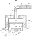
- an etching apparatus 100 is shown in FIG. 1 as an example of a plasma processing apparatus using ECR.
- the etching apparatus 100 for explaining the principle of the present invention includes a substantially cylindrical plasma processing chamber 104. Inside the plasma processing chamber 104, a substrate electrode 120 on which the substrate 106 to be processed is placed, and a dielectric block 121 that electrically insulates between the plasma processing chamber 104 and the substrate electrode 120 are installed. Further, inside the plasma processing chamber 104, an earth electrode 105 that operates as an RF bias ground is provided.
- a cavity 102 is formed in the upper part of the plasma processing chamber 104, and a microwave introduction window 103 and a gas dispersion plate 111 are grounded between the plasma processing chamber 104 and the cavity 102. .. Processing gas, inert gas, etc. are supplied from the gas supply unit 140 between the microwave introduction window 103 and the gas dispersion plate 111, and the plasma processing chamber is provided through a large number of minute holes (not shown) of the gas dispersion plate 111. Gas is supplied to the inside of 104.
- the gas supply unit 140 includes a gas cylinder 143, a switching valve 142 for switching between gas supply and stop, and a gas supply pipe 141 for connecting the switching valve 142 and the plasma processing chamber 104.
- the inside of the plasma processing chamber 104 is exhausted to a vacuum by the exhaust system 150.
- the exhaust system 150 includes an exhaust pipe 151 connected to the plasma processing chamber 104, an openable and closable butterfly valve 152, and a vacuum pump 153.
- the gas supplied from the gas supply unit 140 to the inside of the plasma processing chamber 104 is also exhausted from the plasma processing chamber 104 by the exhaust system 150.
- An electromagnet 101 is installed around the plasma processing chamber 104.
- the electromagnet 101 includes an upper coil 1011 and a lower coil 1012, 1013, and suppresses a magnetic field leaking to the outside on the outer periphery of the upper coil 1011 and the lower coil 1012, 1013, and efficiently concentrates the magnetic field in the plasma processing chamber.
- a yoke 1014 for the purpose is provided.
- a circular waveguide 110 is connected to the cavity 102 along the central axis, and the circular waveguide 110 is connected to the rectangular waveguide 134 via the circular rectangular converter 135.
- a microwave generation source 131, an isolator 132, and an automatic matcher 133 are connected to the rectangular waveguide 134.
- the ECR is provided inside the plasma processing chamber 104 by the electromagnet 101 installed around the substantially cylindrical plasma processing chamber 104.
- a static magnetic field can be applied to wake it up.
- the static magnetic field distribution in the plasma processing chamber 104 can be controlled by adjusting the strength of the magnetic field generated by the multi-stage coils 1011, 1012, 1013 constituting the electromagnet 101.
- the microwave generated at the microwave generation source 131 and passed through the isolator 132 and the automatic matching unit 133 is subjected to the substrate electrode of the plasma processing chamber 104 by the circular waveguide 110 installed along the central axis of the plasma processing chamber 104. It is charged into the plasma processing chamber 104 from the surface facing the substrate 106 to be processed placed on the 120.
- a magnetron with an oscillation frequency of 2.45 GHz was used as the microwave generation source 131.
- the automatic matcher 133 connected to the output side of the microwave source 131 is for suppressing the reflected wave due to impedance mismatch with the isolator 132 for protecting the source.
- the microwave generation source 131 to the automatic matching device 133 were connected by using a rectangular waveguide 134.
- a circular rectangle converter 135 was used for connection with the circular waveguide 110.
- the circular waveguide 110 operates in the TE11 mode, which is the lowest-order mode, and by setting the diameter so that only this lowest-order mode can propagate, the occurrence of the higher-order mode is suppressed and the operation is stabilized.
- a circularly polarized wave generator 109 is provided in the circular waveguide 110 to circularly polarize the microwaves in the TE11 mode.
- the electromagnetic field changes in the azimuth direction with respect to the central axis of the circular waveguide, but by making it circularly polarized by the circularly polarized wave generator 109, the electromagnetic field is not azimuthally oriented in one cycle of microwaves. It has the effect of smoothing the uniformity and ensuring axial symmetry.
- the electron cyclotron resonance phenomenon described later occurs efficiently when a circularly polarized microwave is applied to a plasma to which a static magnetic field is applied, and it also has an effect of increasing the absorption efficiency of microwave power into the plasma.
- the microwave input from the circular waveguide 110 is shaped in the electromagnetic field distribution in the cavity 102, and is input to the plasma processing chamber 104 via the microwave introduction window 103 and the gas dispersion plate 111 provided on the processing chamber side thereof. Will be done. Quartz is often used as a material that allows microwaves to pass through the microwave introduction window 103 and the gas dispersion plate 111 and does not adversely affect plasma processing. Further, the inner surface of the plasma processing chamber 104 is often protected by an inner cylinder made of quartz or the like to prevent damage due to plasma.
- a silicon substrate having a diameter of 300 mm was used as the substrate 106 to be processed.
- An RF (Radio Frequency) power supply 108 is connected to the substrate electrode 120 on which the substrate 106 to be processed is placed via an automatic matching box 107, and the above-mentioned RF bias is applied.
- An RF power source 108 having a frequency of 400 kHz was used.
- the gas emitted from the gas supply unit 140 that supplies the processing gas, the inert gas, etc. to the inside of the plasma processing chamber 104 is gas with the microwave introduction window 103 in the plasma processing chamber 104 by the gas supply pipe 141 via the valve 142. It is supplied between the dispersion plates 111, and is supplied in a shower shape to the inside of the plasma processing chamber 104 through a fine hole (not shown) provided in the gas dispersion plate 111. The distribution of gas supply can be adjusted by arranging the holes in the gas dispersion plate 111.
- the impedance of the path from the substrate 106 to be processed to the ground via plasma is important. That is, it is known that the sheath formed between the substrate 106 to be processed and the plasma has a non-linear impedance, and when an RF bias current flows through this sheath region, the DC potential of the substrate 106 to be processed drops. Ions in the plasma can be drawn in.
- An earth electrode 105 is provided inside the plasma processing chamber 104 in order to allow the RF bias current to flow efficiently.
- the static magnetic field generated by the electromagnet 101 is often set substantially parallel to the microwave input direction. This is because it is known that ECR by microwaves is efficiently generated by a static magnetic field parallel to the traveling direction of microwaves. In the example of Fig. 1, a static magnetic field is applied in the direction along the central axis of the plasma processing chamber.
- the upper part of the plasma processing chamber 104 has a strong static magnetic field and the lower part has a weak static magnetic field, and the magnetic flux density (0.0875 tesla when the microwave frequency is 2.45 GHz) satisfies the ECR condition in the middle.
- the microwave is input from above.
- the setting is such that it is easy to generate a static magnetic field (referred to as a divergent magnetic field) in which the static magnetic field is monotonically weakened from above along the central axis of the electromagnet 101.
- the electromagnet 101 has a structure in which the upper coil 1011 is strong and the lower coils 1012 and 1013 are likely to generate a relatively weak static magnetic field, so that the magnetomotive force of the upper coil 1011 is relative to that of the lower coils 1012 and 1013. It is enlarged to.
- the outer circumference of the electromagnet 101 is often provided with a yoke 1014 for suppressing the magnetic field leaking to the outside and efficiently concentrating the magnetic field in the plasma processing chamber.
- the yoke 1014 is made of a material having a high saturation magnetic flux density, and pure iron is often used because of its price and availability.
- the yoke 1014 is arranged so as to cover the entire plasma processing chamber 104.
- the lower end 1015 of the yoke 1014 extends close to the surface of the substrate 106 to be treated.
- a plurality of waveguides for transmitting microwave power are divided, and microwave radiation means are provided on the processing chamber side of each waveguide.
- the waveguide for transmitting microwaves is composed of a combination of a circular waveguide and a coaxial waveguide having a central axis common to the central axis of the circular waveguide.
- a phenomenon called waveguide cutoff can be used to adjust the microwave power. It is generally known that when the size of the waveguide is smaller than the wavelength of the microwave, the microwave cannot be transmitted, which is called a cutoff. It is also known that by loading a dielectric having a large relative permittivity in the waveguide, the cutoff dimension can be reduced due to the wavelength shortening effect.
- microwaves having a radius of 35.9 mm or less and 2.45 GHz are cut off, and when the medium is quartz, microwaves having a radius of 17.9 mm or more and 2.45 GHz are cut off. You can see that it can be transmitted.
- the waveguide radius is set to 17.9 mm or more and less than 35.9 mm, so that if the medium in the waveguide is air, it will be cut off, and if quartz is loaded, it will be micro. Waveguide can be transmitted.
- the microwave electric field decreases exponentially from the input end of the microwave in the waveguide in the cutoff state. That is, by adjusting the length of the waveguide in the cutoff state, the magnitude of the microwave leaking to the output end can be adjusted.
- a cylinder is coaxially loaded in a circular waveguide, and microwaves can be transmitted when a dielectric is loaded inside the cylinder, and a cutoff is used when the dielectric is not loaded. By freely inserting and removing the dielectric, it is possible to make a cut-off, enable transmission, and adjust. Further, the outer side of the cylinder can be operated as a coaxial waveguide, the microwave power is divided into an inner circular waveguide and an outer coaxial waveguide, and the transmission power of the inner circular waveguide is controlled. Therefore, the division ratio of the microwave power can be controlled.
- the microwave plasma etching apparatus 200 will be described with reference to FIGS. 2 to 7.
- the present inventors have described a method of controlling the density distribution of generated plasma by adjusting the microwave electromagnetic field distribution in the processing chamber based on the etching apparatus 100 shown in FIG. 1 which explains the principle of the present invention. investigated. As a result, the structure shown in FIG. 2 was obtained.
- the parts common to the etching apparatus 100 for explaining the principle of the present invention shown in FIG. 1 are numbered the same. The same part as that described in FIG. 1 including the same number will be omitted, and the differences will be mainly described.
- the configuration of the microwave plasma etching apparatus 200 shown in FIG. 2 is mainly a modification of the internal structures of the circular waveguide 110 and the cavity 102 of the etching apparatus 100 showing the principle of the present invention shown in FIG.
- the microwave plasma etching apparatus 200 includes a microwave generator 131, an isolator 132, and an automatic matcher 133, has an upper coil 1011 and a lower coil 1012, 1013 around the plasma processing chamber 104, and has a yoke 1014 on the outer periphery.
- the point that the power supply 108 is connected is the same as the configuration of the etching apparatus 100 showing the principle of the present invention shown in FIG.
- the first circular waveguide 201 is connected instead of the circular waveguide 110 of the etching apparatus 100 described with reference to FIG.
- a second circular waveguide 202 and a third circular waveguide 204 having a slightly enlarged diameter are arranged inside the waveguide 201 on the output side thereof.
- a circular polarization generator 208 is built in the circular waveguide 2011 connected to the circular rectangular converter 135.
- a first circular waveguide 201 with an enlarged diameter is connected to the lower part of the circular waveguide 2011 corresponding to the output end of the circularly polarized wave generator 208.
- a second circular waveguide 202 and a third circular waveguide 204 having a slightly enlarged diameter are arranged on the output side thereof.
- the circular waveguide 2011, the first circular waveguide 201, the second circular waveguide 202, and the third circular waveguide 204 share a central axis.
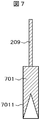
- a dielectric rod 209 is connected to the dielectric 203.
- the rod 209 is arranged on the central axis of the first circular waveguide 201, penetrates the center of the circularly polarized wave generator 208, and protrudes outward from the guide portion 136 provided in the circular rectangular converter 135.
- the amount of the dielectric 203 inserted into the second circular waveguide 202 can be adjusted by inserting and removing (inserting and removing) the portion protruding from the guide portion 136 to the outside from the outside of the circular rectangular converter 135. It is desirable that the dielectric 203 has a material that has a small loss with respect to microwaves and is stable against temperature changes, and quartz is used in this example.
- the dielectric 203 serves as a cutoff frequency control mechanism for the second circular waveguide 202.
- the third circular waveguide 204 needs to have an internal radius of 35.9 mm or more as described above in order to enable microwave transmission when the internal medium is air, and in this embodiment, the radius is 40 mm. did. It is also possible to load the third circular waveguide 204 with a dielectric to reduce the size.
- the inner portion of the first circular waveguide 201 and the outer portion of the third circular waveguide 204 operate as the coaxial waveguide 205.
- a coaxial waveguide can transmit from direct current whose frequency can be regarded as zero, and there is no cutoff, but when operating in higher-order TE mode, there is a cutoff.
- the coaxial waveguide 205 operates in a higher order TE 11 mode.
- the cutoff frequency cannot be calculated by a simple formula, but it is known that the cutoff frequency can be approximately calculated by the formula (Equation 3) in the TE 11 mode of the coaxial waveguide. There is.
- the TE11 mode of the coaxial waveguide 205 is set to a dimension that does not cause a cutoff.
- a flange portion 2041 is formed on the outside of the output end side of the third circular waveguide 204, and the space formed by the flange portion 2041 and the circular tube 2043 acts as the inner antenna 206.
- the diameter of the circular tube 2043 is increased to open the side of the microwave introduction window 103.
- the cylindrical hollow inner antenna 206 can generate plasma having a convex distribution on the substrate 106 to be processed in the plasma processing chamber 104.
- FIG. 3 shows a cross-sectional view taken along the line AA in FIG. 2
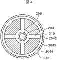
- FIG. 4 shows a cross-sectional view taken along the line BB.
- the waveguide 210 is formed by the waveguide forming portion 2044 in the space sandwiched between the cavity 212 and the flange 2041.
- the space surrounded by the circular pipe 2043, the flange portion 2042 outside the circular pipe 2043, the hollow portion 212, and the disk 2120 connected to the hollow portion 212 is the flange portion 2042 and the hollow portion 212.
- the outer antenna 207 is connected to the waveguide 210 through the gap 2045 between them.
- the outer antenna 207 in this embodiment forms a ring-shaped cavity resonator, but another structure may be used as long as the antenna can obtain an outer height distribution on the substrate 106 to be processed.
- the outer antenna 207 having a ring-shaped cavity resonator structure uses a slot 2101 extended in the azimuth direction for connection with the waveguide 210. Further, for radiating microwaves to the plasma processing chamber 104, an annular slot with a gap 222 between the circular tube 2043 and the disk 2120 was used, but other structures such as a slot in the radial direction may also be used. good.
- a space 211 is provided between the inner antenna 206, the outer antenna 207, and the quartz microwave introduction window 103.
- the height of space 211 can be adjusted to alleviate microwave inconsistencies.
- the second circular waveguide 202 When the rod 209 is pulled up from the side of the guide portion 136 and the dielectric 203 is pulled out from the second circular waveguide 202, the second circular waveguide 202 is in a cutoff state with respect to microwaves, and the inner antenna 206 is reached. Microwave supply is cut off. As a result, the microwave is not radiated from the inner antenna 206 to the plasma processing chamber 104, and is radiated from only the outer antenna 207 into the plasma processing chamber 104.
- the dielectric 203 is loaded on the second circular waveguide 202 and can be transmitted. ..
- microwaves are supplied from the third circular waveguide 204 to the inner antenna 206, and microwaves are supplied from both the inner antenna 206 and the outer antenna 207 into the plasma processing chamber 104.
- the rod 209 is supplied to the inner antenna 206 and the outer antenna 207.
- the microwave power ratio can be changed. Since the distribution of plasma generated by the inner antenna 206 and the outer antenna 207 is different, the position of the dielectric 203 is changed to adjust the microwave power ratio supplied to the inner antenna 206 and the outer antenna 207, so that the plasma processing chamber 104 It is possible to control the plasma distribution in.
- the dielectric 203 shown in FIG. 2 has a simple cylindrical shape, but the tip portion 6011 of the dielectric 601 is sharpened as shown in FIG. 6 (dielectric 401), or the cross section is shown in FIG. A tapered cavity may be added to the tip portion 7021 of the dielectric 702 (dielectric 501).
- the equivalent relative permittivity changes slowly, so that the second of the dielectrics 601 or 701
- the change in microwave power transmittance with respect to the amount inserted into the circular waveguide 202 can be moderated. This has the effect of improving the accuracy of microwave power control.
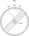
- FIG. 5 is a cross-sectional view in the direction perpendicular to the central axis of the circular waveguide 2011.
- a known structure composed of a dielectric plate arranged at an angle of 45 degrees with respect to the electric field direction of the circular waveguide 2011 in the TE11 mode was used. Quartz was used as the dielectric.
- a hole 2081 for passing the rod 209 is provided in the circularly polarized wave generator 208.
- the material of the rod 209 is the same quartz as that of the circularly polarized wave generator 208.
- the relative permittivity of the holes decreases, so the equivalent permittivity of the entire plate decreases, and the efficiency of circularly polarized wave generation decreases.
- aligning the materials of the rod 209 and making the diameter of the hole and the diameter of the rod substantially the same it is possible to prevent an equivalent decrease in the dielectric constant and prevent a decrease in the circular polarization generation efficiency.
- the ratio of the microwave power supplied to the internal and external antennas can be adjusted by the positions of the rod 209 and the dielectric 203, whereby the distribution of plasma generated in the processing chamber can be controlled. If it is not necessary to frequently adjust the power ratio supplied to the inner and outer antennas, the rod 209 may be omitted and the position of the dielectric 203 may be semi-fixed. Although the ease of plasma distribution control is impaired, there is an advantage that a drive mechanism such as a rod can be omitted and the structure can be simplified.
- the plasma density distribution on the substrate to be processed tends to be convex and flat, especially under the condition that the processing chamber pressure is high.
- the plasma processing apparatus having the configuration as described in this embodiment it becomes easy to obtain a flat distribution of the plasma density, and this problem can be solved.
- the distribution of the density of plasma generated in the processing chamber by each antenna is adjusted by adjusting the magnitude of each microwave power radiated from a plurality of antennas.
- the microwave power supplied to the inner and outer antennas can be adjusted to control the degree of outside height and middle-high distribution of the plasma.
- the distribution of the density of the plasma generated in the processing chamber can be adjusted, the local area due to the plasma of the dielectric window portion that transmits microwaves while keeping the vacuum processing chamber airtight. It is possible to suppress the scraping, and it is possible to improve the uniformity of the plasma treatment applied to the substrate to be processed as compared with the case where the configuration as in this embodiment is not adopted.
- Electromagnetic magnet 102 Cavity 103 Microwave introduction window 104 Plasma processing room 105 Earth electrode 106 Processed substrate 107 Automatic matching device 108 RF power supply 109 Circular polarization generator 110 Circular waveguide 201 1st circular waveguide 202 2nd circular Waveguide 203 Dielectric 204 Third Circular Waveguide 205 Coaxial Waveguide 206 Inner Antenna 207 Outer Antenna 208 Circular Waveguide 209 Rod 210 Waveguide 211 Space 401 Dielectric 501 Dielectric
Abstract
In order to provide a plasma treatment device that can easily control the plasma density distribution on a substrate to be processed, the plasma treatment device comprises: a microwave generation source for generating microwaves; a waveguide provided with a waveguide tube that conveys microwaves generated by the microwave generation source to a processing chamber; a processing chamber internally provided with a mounting platform on which the substrate to be processed is mounted, the processing chamber connecting to the waveguide; a gas introduction unit that introduces gas to the interior of the processing chamber; and an exhaust unit that discharges, to outside the processing chamber, the gas that was introduced to the interior of the processing chamber, wherein the portion of the waveguide that is connected to the processing chamber is configured from a plurality of coaxially formed waveguide tubes.
Description
本発明は、電磁波によりプラズマを発生させるプラズマ処理装置に関する。
The present invention relates to a plasma processing apparatus that generates plasma by electromagnetic waves.
半導体集積回路素子の生産にプラズマ処理装置が用いられている。電磁波によりプラズマを発生するプラズマ処理装置において、静磁界をプラズマ処理室に加えた装置が広く用いられている。静磁界によりプラズマの損失を抑制することができるほか、プラズマ分布の制御も可能となる利点があるためである。さらに電磁波と静磁界の相互作用を用いることで、通常はプラズマ発生が困難な運転条件でも発生可能とできる効果がある。
Plasma processing equipment is used in the production of semiconductor integrated circuit elements. In a plasma processing device that generates plasma by electromagnetic waves, a device in which a static magnetic field is applied to a plasma processing chamber is widely used. This is because the static magnetic field has the advantage that the plasma loss can be suppressed and the plasma distribution can be controlled. Furthermore, by using the interaction between electromagnetic waves and static magnetic fields, there is an effect that plasma can be generated even under operating conditions where it is usually difficult to generate plasma.
特にプラズマ発生用電磁波としてマイクロ波を用い、電子のサイクロトロン運動の周期とマイクロ波の周波数を一致させる静磁界を用いると、電子サイクロトロン共鳴(Electron Cyclotron Resonance、以下ECRと称する)現象が起きることが知られている。ECRが起きる領域で主にプラズマが発生することから、静磁界の分布を調節することでプラズマ発生領域の制御が可能となるほか、ECR現象によりプラズマ生成可能な条件が広く確保できる効果がある。
In particular, it is known that when microwaves are used as electromagnetic waves for plasma generation and a static magnetic field that matches the period of electron cyclotron motion and the frequency of microwaves is used, an electron cyclotron resonance (Electron Cyclotron Resonance, hereinafter referred to as ECR) phenomenon occurs. Has been done. Since plasma is mainly generated in the region where ECR occurs, it is possible to control the plasma generation region by adjusting the distribution of the static magnetic field, and there is an effect that the conditions under which plasma can be generated can be widely secured by the ECR phenomenon.
プラズマ処理中の被処理基板に高周波を印加し、プラズマ中のイオンを被処理基板表面に引き込むことでプラズマ処理の高速化や処理品質の向上を図るRFバイアス技術が用いられている。例えばプラズマエッチング処理の場合、被処理基板の被処理面に垂直にイオンが入射するため、エッチングが被処理基板の垂直方向にのみ進む異方性の加工が達成される。
RF bias technology is used to speed up plasma processing and improve processing quality by applying high frequencies to the substrate to be processed during plasma processing and drawing ions in the plasma to the surface of the substrate to be processed. For example, in the case of plasma etching processing, since ions are vertically incident on the surface to be processed of the substrate to be processed, anisotropic processing in which etching proceeds only in the vertical direction of the substrate to be processed is achieved.
特許文献1には、処理室の中心軸と同心に設置されたプラズマ発生用電磁波導入経路と、電磁波を複数の出力ポートに分配する分岐回路と、分岐回路の出力ポートに接続され、前記プラズマ発生用電磁波の導入経路と同心に設置されたリング状空洞共振器とを備えたプラズマ処理装置において、プラズマ発生用電磁波導入経路が円形導波管により構成することにより、リング状空洞共振器内に進行波を励振することで、定在波に起因するプラズマ密度の空間的な変動を防止でき、均一なプラズマ処理を可能とすることが記載されている。
In Patent Document 1, the electromagnetic wave introduction path for plasma generation installed concentrically with the central axis of the processing chamber, the branch circuit that distributes the electromagnetic wave to a plurality of output ports, and the output port of the branch circuit are connected to generate the plasma. In a plasma processing device provided with a ring-shaped cavity resonator installed concentrically with the introduction path of the electromagnetic wave for plasma generation, the introduction path of the electromagnetic wave for plasma generation proceeds in the ring-shaped cavity resonator by being configured by a circular waveguide. It is described that by exciting the wave, it is possible to prevent the spatial fluctuation of the plasma density due to the standing wave, and to enable uniform plasma processing.
プラズマ発生用電力としてマイクロ波を用いる場合、マイクロ波電力を伝達するのに導波管が用いられるが、一般に導波管の寸法がマイクロ波の波長に比べて小さい場合に、マイクロ波が伝送できなくなることが知られており、カットオフと呼ばれる。非特許文献1には、円形導波管の場合について円形導波管の寸法とカットオフ周波数との関係について記載されている。
When microwaves are used as the power for generating plasma, a waveguide is used to transmit the microwave power. Generally, when the size of the waveguide is smaller than the wavelength of the microwave, the microwave can be transmitted. It is known to disappear and is called a cutoff. Non-Patent Document 1 describes the relationship between the dimensions of the circular waveguide and the cutoff frequency in the case of the circular waveguide.
一般にプラズマはプラズマ処理室壁面で損失することが多く、壁面付近では密度が低く、壁面から離れた中心付近で密度が高くなる傾向がある。こういったプラズマ密度分布の不均一に起因する処理の不均一が問題となることがある。静磁界を用いたプラズマ処理装置では、プラズマ生成条件によってはプラズマ処理室の中心付近で密度が高くなる場合がある。これに対応し被処理基板上のプラズマ密度が凸分布となりやすい傾向があり、プラズマ処理の均一性が問題となることがある。
In general, plasma is often lost on the wall surface of the plasma processing chamber, and the density tends to be low near the wall surface and high near the center away from the wall surface. Non-uniformity of processing due to such non-uniformity of plasma density distribution can be a problem. In a plasma processing apparatus using a static magnetic field, the density may increase near the center of the plasma processing chamber depending on the plasma generation conditions. Correspondingly, the plasma density on the substrate to be processed tends to be convexly distributed, and the uniformity of plasma processing may become a problem.
プラズマは磁力線に沿う方向には拡散しやすいが、磁力線と垂直方向には拡散が抑制される性質がある。さらに静磁界の分布を調整することで、ECR面などの位置を調整してプラズマ発生領域の制御が可能である。このように静磁界の分布を調整することでプラズマの分布を調整することができる。
Plasma tends to diffuse in the direction along the magnetic field line, but has the property of suppressing diffusion in the direction perpendicular to the magnetic field line. Furthermore, by adjusting the distribution of the static magnetic field, it is possible to control the plasma generation region by adjusting the position of the ECR surface and the like. By adjusting the distribution of the static magnetic field in this way, the distribution of plasma can be adjusted.
しかし静磁界によるプラズマ密度分布の調整手段のみでは所望の調整幅が得られない場合があり、さらに追加の調整手段が望まれている。
However, the desired adjustment range may not be obtained only by the means for adjusting the plasma density distribution by the static magnetic field, and further adjustment means are desired.
例えばエッチング処理の場合、加工する膜厚が成膜装置の特性に応じて、例えば処理基板の中央で厚く外周側で薄い場合、逆に中央で薄く外周側で厚い場合、があり得る。これらの成膜装置起因の不均一をエッチング処理で補正して、全体で均一な加工を施したい場合がある。このように被処理基板上でのプラズマ密度分布を所望の分布に調整することが望まれる場合がある。
For example, in the case of etching treatment, the film thickness to be processed may be thick in the center of the processing substrate and thin on the outer peripheral side, or conversely thin in the center and thick on the outer peripheral side, depending on the characteristics of the film forming apparatus. In some cases, it may be desired to correct the non-uniformity caused by these film forming apparatus by etching processing and perform uniform processing as a whole. In this way, it may be desired to adjust the plasma density distribution on the substrate to be processed to a desired distribution.
一般にエッチング速度が均一であれば、反応生成物は被処理基板各部から均一に生成し放出される。その結果、被処理基板の中心部では反応生成物密度が高く、外周部では密度が低くなる。反応生成物が被処理基板に再付着すると、エッチングが阻害されてエッチング速度が低下する。反応生成物が被処理基板に再付着する確率は、被処理基板の温度や処理室の圧力、被処理基板の表面状態等、多くのパラメータに影響される。そのため被処理基板の面内で均一なエッチング処理を得るためには、被処理基板上のプラズマ密度分布を中高、あるいは外高に調整しなければならない場合がある。
Generally, if the etching rate is uniform, the reaction product is uniformly generated and released from each part of the substrate to be processed. As a result, the reaction product density is high in the central portion of the substrate to be processed, and the density is low in the outer peripheral portion. When the reaction product reattaches to the substrate to be processed, etching is hindered and the etching rate decreases. The probability that the reaction product will reattach to the substrate to be processed is affected by many parameters such as the temperature of the substrate to be processed, the pressure in the processing chamber, and the surface condition of the substrate to be processed. Therefore, in order to obtain a uniform etching process in the plane of the substrate to be processed, it may be necessary to adjust the plasma density distribution on the substrate to be processed to medium or high.
上記に示すように被処理基板上でのプラズマ密度分布を容易に制御できるようにするプラズマ処理装置の構成として、特許文献1において、リング状空洞共振器内の電磁界は定在波を形成する。例えば、電界の定在波が形成される場合、電界強度の強い腹部、電界強度の弱い節部が存在する。これらの腹節の位置は固定されており、プラズマ処理室内にも空洞共振器内の電界強度腹節に対応した電界強度の強弱が発生する場合がある。
As shown above, as a configuration of the plasma processing apparatus that enables the plasma density distribution on the substrate to be processed to be easily controlled, in Patent Document 1, the electromagnetic field in the ring-shaped cavity resonator forms a standing wave. .. For example, when a standing wave of an electric field is formed, there is an abdomen with a strong electric field strength and a node with a weak electric field strength. The positions of these abdominal segments are fixed, and the strength of the electric field strength corresponding to the electric field strength abdominal segment in the cavity resonator may occur in the plasma processing chamber.
この電界強度の強弱により、処理室内に発生するプラズマも不均一となる場合がある。この不均一により真空処理室を気密に保持しつつマイクロ波を透過させる誘電体窓部のプラズマによる削れが局所的に大きくなる、被処理基板に施すプラズマ処理の均一性に悪影響を与える、等の不具合が生じる場合がある。
Depending on the strength of this electric field strength, the plasma generated in the processing chamber may also be non-uniform. Due to this non-uniformity, the scraping of the dielectric window portion that transmits microwaves while keeping the vacuum treatment chamber airtight is locally increased, and the uniformity of plasma treatment applied to the substrate to be treated is adversely affected. Problems may occur.
本発明は、上記した従来技術の課題を解決して、被処理基板上でのプラズマ密度分布を容易に制御できるプラズマ処理装置を提供するものである。
The present invention solves the above-mentioned problems of the prior art and provides a plasma processing apparatus capable of easily controlling the plasma density distribution on the substrate to be processed.
上記した課題を解決するために、本発明では、プラズマ処理装置を、試料がプラズマ処理される処理室と、プラズマを生成するためのマイクロ波の高周波電力を導波路を介して供給する高周波電源と、処理室の内部に磁場を形成する磁場形成機構と、カットオフ周波数を制御するカットオフ周波数制御機構とを備えて構成し、導波路は、円形導波管と、この円形導波管の外側に配置され円形導波管と同軸上に配置された同軸導波管と、を具備し、
カットオフ周波数制御機構は、円形導波管のカットオフ周波数を制御するようにした。 In order to solve the above-mentioned problems, in the present invention, the plasma processing apparatus is provided with a processing chamber in which the sample is plasma-processed and a high-frequency power source that supplies high-frequency microwave power for generating plasma via a waveguide. , A magnetic field forming mechanism that forms a magnetic field inside the processing chamber and a cutoff frequency control mechanism that controls the cutoff frequency are provided, and the waveguide is a circular waveguide and the outside of this circular waveguide. A coaxial waveguide arranged coaxially with a circular waveguide provided in the
The cutoff frequency control mechanism is designed to control the cutoff frequency of the circular waveguide.
本発明によれば、被処理基板上でのプラズマ密度分布を容易に制御できるプラズマ処理装置を提供することができる。
According to the present invention, it is possible to provide a plasma processing apparatus capable of easily controlling the plasma density distribution on the substrate to be processed.
本発明では、高品質なプラズマ処理を可能とするプラズマ処理装置を提供するものである。本発明では、プラズマ処理装置において、特にマイクロ波電力の分布を調整することで処理室内に生成するプラズマの分布を制御できるようにしたプラズマ処理装置に関するものである。
The present invention provides a plasma processing apparatus capable of high-quality plasma processing. The present invention relates to a plasma processing apparatus in which the distribution of plasma generated in the processing chamber can be controlled by adjusting the distribution of microwave electric power.
本発明の原理を説明するために、ECRを用いたプラズマ処理装置の例として、図1にエッチング装置100を示す。本発明の原理を説明するためのエッチング装置100は、略円筒状のプラズマ処理室104を備えている。プラズマ処理室104の内部には、被処理基板106を載置する基板電極120、プラズマ処理室104と基板電極120との間を電気的に絶縁する誘電体ブロック121が設置されている。更に、プラズマ処理室104の内部には、RFバイアスのアースとして動作するアース電極105が設けられている。
In order to explain the principle of the present invention, an etching apparatus 100 is shown in FIG. 1 as an example of a plasma processing apparatus using ECR. The etching apparatus 100 for explaining the principle of the present invention includes a substantially cylindrical plasma processing chamber 104. Inside the plasma processing chamber 104, a substrate electrode 120 on which the substrate 106 to be processed is placed, and a dielectric block 121 that electrically insulates between the plasma processing chamber 104 and the substrate electrode 120 are installed. Further, inside the plasma processing chamber 104, an earth electrode 105 that operates as an RF bias ground is provided.
一方、プラズマ処理室104の上部には、空洞部102が形成されており、プラズマ処理室104と空洞部102との間には、マイクロ波導入窓103と、ガス分散板111が接地されている。マイクロ波導入窓103とガス分散板111との間には、ガス供給部140から処理ガスや不活性ガスなどが供給され、ガス分散板111の図示していない多数の微細な穴からプラズマ処理室104の内部にガスを供給する。
On the other hand, a cavity 102 is formed in the upper part of the plasma processing chamber 104, and a microwave introduction window 103 and a gas dispersion plate 111 are grounded between the plasma processing chamber 104 and the cavity 102. .. Processing gas, inert gas, etc. are supplied from the gas supply unit 140 between the microwave introduction window 103 and the gas dispersion plate 111, and the plasma processing chamber is provided through a large number of minute holes (not shown) of the gas dispersion plate 111. Gas is supplied to the inside of 104.
ガス供給部140は、ガスボンベ143、ガスの供給と停止を切り替える切換えバルブ142、切換えバルブ142とプラズマ処理室104との間を接続するガス供給管141を備えている。
The gas supply unit 140 includes a gas cylinder 143, a switching valve 142 for switching between gas supply and stop, and a gas supply pipe 141 for connecting the switching valve 142 and the plasma processing chamber 104.
プラズマ処理室104の内部は、排気系150により真空に排気される。排気系150は、プラズマ処理室104に接続された排気管151、開閉可能なバタフライバルブ152、真空ポンプ153を備えている。これにより、ガス供給部140からプラズマ処理室104の内部に供給されたガスも、排気系150によりプラズマ処理室104から排気される。
The inside of the plasma processing chamber 104 is exhausted to a vacuum by the exhaust system 150. The exhaust system 150 includes an exhaust pipe 151 connected to the plasma processing chamber 104, an openable and closable butterfly valve 152, and a vacuum pump 153. As a result, the gas supplied from the gas supply unit 140 to the inside of the plasma processing chamber 104 is also exhausted from the plasma processing chamber 104 by the exhaust system 150.
プラズマ処理室104の周囲には、電磁石101が設置されている。電磁石101は、上側コイル1011、下側コイル1012,1013を備え、これら上側コイル1011、下側コイル1012,1013の外周には外部に漏洩する磁場の抑制とプラズマ処理室に効率よく磁場を集中させるためのヨーク1014が設けられている。
An electromagnet 101 is installed around the plasma processing chamber 104. The electromagnet 101 includes an upper coil 1011 and a lower coil 1012, 1013, and suppresses a magnetic field leaking to the outside on the outer periphery of the upper coil 1011 and the lower coil 1012, 1013, and efficiently concentrates the magnetic field in the plasma processing chamber. A yoke 1014 for the purpose is provided.
空洞部102には、中心軸に沿って円形導波管110が接続され、円形導波管110は円矩形変換器135を介して矩形導波管134と接続されている。矩形導波管134にはマイクロ波発生源131、アイソレータ132、自動整合器133が接続されている。
A circular waveguide 110 is connected to the cavity 102 along the central axis, and the circular waveguide 110 is connected to the rectangular waveguide 134 via the circular rectangular converter 135. A microwave generation source 131, an isolator 132, and an automatic matcher 133 are connected to the rectangular waveguide 134.
上記したような構成を備えた本発明の原理を説明するためのエッチング装置100においては、略円筒状のプラズマ処理室104の周囲に設置された電磁石101により、プラズマ処理室104の内部にECRを起こすための静磁界を加えることができる。電磁石101を構成する多段のコイル1011,1012,1013により発生する磁場の強さを調整することで、プラズマ処理室104内の静磁界分布を制御できる。
In the etching apparatus 100 for explaining the principle of the present invention having the above-described configuration, the ECR is provided inside the plasma processing chamber 104 by the electromagnet 101 installed around the substantially cylindrical plasma processing chamber 104. A static magnetic field can be applied to wake it up. The static magnetic field distribution in the plasma processing chamber 104 can be controlled by adjusting the strength of the magnetic field generated by the multi-stage coils 1011, 1012, 1013 constituting the electromagnet 101.
マイクロ波発生源131で発生してアイソレータ132、自動整合器133を通ったマイクロ波は、プラズマ処理室104の中心軸に沿って設置された円形導波管110により、プラズマ処理室104の基板電極120上に載置された被処理基板106と対向する面からプラズマ処理室104に投入される。発振周波数2.45GHzのマグネトロンをマイクロ波発生源131として用いた。
The microwave generated at the microwave generation source 131 and passed through the isolator 132 and the automatic matching unit 133 is subjected to the substrate electrode of the plasma processing chamber 104 by the circular waveguide 110 installed along the central axis of the plasma processing chamber 104. It is charged into the plasma processing chamber 104 from the surface facing the substrate 106 to be processed placed on the 120. A magnetron with an oscillation frequency of 2.45 GHz was used as the microwave generation source 131.
マイクロ波発生源131の出力側に接続した自動整合器133は、発生源保護用のアイソレータ132とインピーダンス不整合による反射波を抑制するためのものである。マイクロ波発生源131から自動整合器133までは矩形導波管134を用いて接続した。円形導波管110との接続には円矩形変換器135を用いた。
The automatic matcher 133 connected to the output side of the microwave source 131 is for suppressing the reflected wave due to impedance mismatch with the isolator 132 for protecting the source. The microwave generation source 131 to the automatic matching device 133 were connected by using a rectangular waveguide 134. A circular rectangle converter 135 was used for connection with the circular waveguide 110.
円形導波管110は最低次モードであるTE11モードで動作し、この最低次モードのみが伝搬できる直径とすることで、高次モードの発生を抑制して、動作の安定化を図っている。円形導波管110には円偏波発生器109が設けられ、TE11モードのマイクロ波を円偏波化している。
The circular waveguide 110 operates in the TE11 mode, which is the lowest-order mode, and by setting the diameter so that only this lowest-order mode can propagate, the occurrence of the higher-order mode is suppressed and the operation is stabilized. A circularly polarized wave generator 109 is provided in the circular waveguide 110 to circularly polarize the microwaves in the TE11 mode.
TE11モードは円形導波管の中心軸に対して方位角方向に電磁界が変化するが、円偏波発生器109により円偏波化することで、マイクロ波の1周期で方位角方向の不均一が平滑化され、軸対称性を確保できる効果がある。そのほか静磁界を印加したプラズマに円偏波化したマイクロ波を投入すると後述の電子サイクロトロン共鳴現象が効率よく起きることが知られており、プラズマへのマイクロ波電力の吸収効率を高める効果もある。
In TE11 mode, the electromagnetic field changes in the azimuth direction with respect to the central axis of the circular waveguide, but by making it circularly polarized by the circularly polarized wave generator 109, the electromagnetic field is not azimuthally oriented in one cycle of microwaves. It has the effect of smoothing the uniformity and ensuring axial symmetry. In addition, it is known that the electron cyclotron resonance phenomenon described later occurs efficiently when a circularly polarized microwave is applied to a plasma to which a static magnetic field is applied, and it also has an effect of increasing the absorption efficiency of microwave power into the plasma.
円形導波管110から投入されたマイクロ波は空洞部102で電磁界分布を整形され、マイクロ波導入窓103とその処理室側に設けられたガス分散板111を介してプラズマ処理室104に投入される。マイクロ波導入窓103、ガス分散板111はマイクロ波を透過し、プラズマ処理に悪影響を与えにくい材質として石英を用いることが多い。またプラズマ処理室104の内面は石英等の内筒で保護することで、プラズマによる損傷を防止することが多い。
The microwave input from the circular waveguide 110 is shaped in the electromagnetic field distribution in the cavity 102, and is input to the plasma processing chamber 104 via the microwave introduction window 103 and the gas dispersion plate 111 provided on the processing chamber side thereof. Will be done. Quartz is often used as a material that allows microwaves to pass through the microwave introduction window 103 and the gas dispersion plate 111 and does not adversely affect plasma processing. Further, the inner surface of the plasma processing chamber 104 is often protected by an inner cylinder made of quartz or the like to prevent damage due to plasma.
直径300mmのシリコン基板を被処理基板106として用いた。被処理基板106を載置する基板電極120には、自動整合器(マッチングボックス)107を介してRF(Radio Frequency)電源108が接続され、前述のRFバイアスが印加される。RF電源108として周波数400kHzのものを用いた。
A silicon substrate having a diameter of 300 mm was used as the substrate 106 to be processed. An RF (Radio Frequency) power supply 108 is connected to the substrate electrode 120 on which the substrate 106 to be processed is placed via an automatic matching box 107, and the above-mentioned RF bias is applied. An RF power source 108 having a frequency of 400 kHz was used.
プラズマ処理室104の内部に処理ガスや不活性ガスなどを供給するガス供給部140から出たガスは、バルブ142を介してガス供給管141によりプラズマ処理室104内でマイクロ波導入窓103とガス分散板111の間に供給され、ガス分散板111に設けた図示していない微細な穴を通してプラズマ処理室104の内部にシャワー状に供給される。ガス分散板111の穴の配置により、ガス供給の分布を調整することができる。
The gas emitted from the gas supply unit 140 that supplies the processing gas, the inert gas, etc. to the inside of the plasma processing chamber 104 is gas with the microwave introduction window 103 in the plasma processing chamber 104 by the gas supply pipe 141 via the valve 142. It is supplied between the dispersion plates 111, and is supplied in a shower shape to the inside of the plasma processing chamber 104 through a fine hole (not shown) provided in the gas dispersion plate 111. The distribution of gas supply can be adjusted by arranging the holes in the gas dispersion plate 111.
前述のRFバイアス技術を適用するには、被処理基板106からプラズマを介してアースにいたる経路のインピーダンスが重要となる。すなわち被処理基板106とプラズマの間に形成されるシースは非線形性のインピーダンスを持つことが知られており、このシース領域をRFバイアス電流が流れることで、被処理基板106のDC電位が下がり、プラズマ中のイオンを引き込むことができる。RFバイアス電流を効率よく流すために、プラズマ処理室104の内部にアース電極105が設けられている。
In order to apply the above-mentioned RF bias technology, the impedance of the path from the substrate 106 to be processed to the ground via plasma is important. That is, it is known that the sheath formed between the substrate 106 to be processed and the plasma has a non-linear impedance, and when an RF bias current flows through this sheath region, the DC potential of the substrate 106 to be processed drops. Ions in the plasma can be drawn in. An earth electrode 105 is provided inside the plasma processing chamber 104 in order to allow the RF bias current to flow efficiently.
電磁石101による静磁界はマイクロ波の投入方向と概ね平行に設定されることが多い。マイクロ波によるECRはマイクロ波の進行方向と平行な静磁界により効率よく起きることが知られているためである。図1の例ではプラズマ処理室の中心軸に沿った方向に静磁界を加える構成としている。
The static magnetic field generated by the electromagnet 101 is often set substantially parallel to the microwave input direction. This is because it is known that ECR by microwaves is efficiently generated by a static magnetic field parallel to the traveling direction of microwaves. In the example of Fig. 1, a static magnetic field is applied in the direction along the central axis of the plasma processing chamber.
磁化プラズマ中マイクロ波の伝播特性は理論的にある程度解明されており、静磁界に沿う方向に伝播するR波と呼ばれる円偏波は、ECR条件の静磁界を越える強磁場領域でプラズマの密度に関係なくプラズマ中を伝播できることが知られている。また前述のECR条件を満たす箇所でマイクロ波の電力は電子にきわめて効率よく吸収されることが知られている。そのためECR条件を満たす箇所にマイクロ波電力を効率よく伝播させるために、強磁場域からマイクロ波を投入し、プラズマ中を伝播させることが行われる。
The propagation characteristics of microwaves in magnetized plasma have been clarified to some extent theoretically, and the circularly polarized waves called R waves propagating in the direction along the static magnetic field become the plasma density in the strong magnetic field region exceeding the static magnetic field under the ECR condition. It is known that it can propagate in plasma regardless. It is also known that microwave power is absorbed extremely efficiently by electrons at locations that satisfy the above-mentioned ECR conditions. Therefore, in order to efficiently propagate the microwave power to the place where the ECR condition is satisfied, the microwave is injected from the strong magnetic field region and propagated in the plasma.
図1に示す例ではプラズマ処理室104の上部に強い静磁界、下部に弱い静磁界とし中間にECR条件を満足する磁束密度(マイクロ波の周波数が2.45GHzの場合0.0875テスラ)となるよう設定して、上側からマイクロ波を投入している。電磁石101の中心軸に沿って上側から単調に静磁界が弱くなる静磁界(発散磁場と称する)を発生させやすい設定としている。すなわち電磁石101はその構成として上側コイル1011が強く、下側コイル1012,1013で相対的に弱い静磁界を発生させやすい様に、上側コイル1011の起磁力を下側コイル1012,1013に比べ相対的に大きくしている。
In the example shown in FIG. 1, the upper part of the plasma processing chamber 104 has a strong static magnetic field and the lower part has a weak static magnetic field, and the magnetic flux density (0.0875 tesla when the microwave frequency is 2.45 GHz) satisfies the ECR condition in the middle. The microwave is input from above. The setting is such that it is easy to generate a static magnetic field (referred to as a divergent magnetic field) in which the static magnetic field is monotonically weakened from above along the central axis of the electromagnet 101. That is, the electromagnet 101 has a structure in which the upper coil 1011 is strong and the lower coils 1012 and 1013 are likely to generate a relatively weak static magnetic field, so that the magnetomotive force of the upper coil 1011 is relative to that of the lower coils 1012 and 1013. It is enlarged to.
電磁石101の外周には外部に漏洩する磁場の抑制とプラズマ処理室に効率よく磁場を集中させるためのヨーク1014が設けられることが多い。ヨーク1014は飽和磁束密度の高い材質で作ることが望ましく、価格や入手のしやすさから、純鉄が用いられることが多い。プラズマ処理室104内に効率よく静磁界を加えるため、ヨーク1014はプラズマ処理室104の全体を覆うように配置される。ヨーク1014の下端1015は被処理基板106の存在する面の近くにまで延伸されている。
The outer circumference of the electromagnet 101 is often provided with a yoke 1014 for suppressing the magnetic field leaking to the outside and efficiently concentrating the magnetic field in the plasma processing chamber. It is desirable that the yoke 1014 is made of a material having a high saturation magnetic flux density, and pure iron is often used because of its price and availability. In order to efficiently apply a static magnetic field into the plasma processing chamber 104, the yoke 1014 is arranged so as to cover the entire plasma processing chamber 104. The lower end 1015 of the yoke 1014 extends close to the surface of the substrate 106 to be treated.
図1で説明した本発明の原理を説明する構成に対して、本発明においては、マイクロ波電力を伝送する導波路を複数分割し、各導波路の処理室側にそれぞれマイクロ波の放射手段を設け、さらに各導波路を伝搬するマイクロ波の電力を調整する手段を設けることで、処理室内のマイクロ波電磁界の分布を調整し、生成するプラズマの分布を制御するようにした。
In contrast to the configuration for explaining the principle of the present invention described with reference to FIG. 1, in the present invention, a plurality of waveguides for transmitting microwave power are divided, and microwave radiation means are provided on the processing chamber side of each waveguide. By providing a means for adjusting the power of the microwave propagating in each waveguide, the distribution of the microwave electromagnetic field in the processing chamber is adjusted and the distribution of the generated plasma is controlled.
これらの構造はすべて同心状に構成されており、マイクロ波、プラズマに非軸対称性が生じることを防止する。すなわちマイクロ波を伝送する導波路は円形導波管とこの円形導波管の中心軸と共通の中心軸を有する同軸導波管の組み合わせで構成した。以下に、本発明の原理について説明する。
All of these structures are concentrically configured to prevent non-axisymmetric symmetry in microwaves and plasma. That is, the waveguide for transmitting microwaves is composed of a combination of a circular waveguide and a coaxial waveguide having a central axis common to the central axis of the circular waveguide. The principle of the present invention will be described below.
マイクロ波電力の調整には導波管のカットオフと呼ばれる現象を用いることができる。一般に導波管の寸法がマイクロ波の波長に比べて小さい場合に、マイクロ波が伝送できなくなることが知られており、カットオフと呼ばれる。また導波管内に比誘電率が大きな誘電体を装荷することで波長短縮効果によりカットオフとなる寸法が小さくできることが知られている。
A phenomenon called waveguide cutoff can be used to adjust the microwave power. It is generally known that when the size of the waveguide is smaller than the wavelength of the microwave, the microwave cannot be transmitted, which is called a cutoff. It is also known that by loading a dielectric having a large relative permittivity in the waveguide, the cutoff dimension can be reduced due to the wavelength shortening effect.
円形導波管の場合、非特許文献1に記載のように式(数1)で示されることが知られている。
In the case of a circular waveguide, it is known that it is represented by the equation (Equation 1) as described in Non-Patent Document 1.

さらにカットオフ波数は式(数2)となる。
Furthermore, the cutoff wavenumber is given by Equation (Equation 2).

すなわち円形導波管内の媒質が空気の場合、半径35.9mm以下で2.45GHzのマイクロ波がカットオフとなり、媒質が石英の場合、半径17.9mm以上の径で2.45GHzのマイクロ波が伝送できることがわかる。
That is, when the medium in the circular waveguide is air, microwaves having a radius of 35.9 mm or less and 2.45 GHz are cut off, and when the medium is quartz, microwaves having a radius of 17.9 mm or more and 2.45 GHz are cut off. You can see that it can be transmitted.
以上よりマイクロ波の周波数が2.45GHzの場合、導波管半径を17.9mm以上35.9mm未満とすることで、導波管内の媒質が空気であればカットオフ、石英を装荷すればマイクロ波電力を伝送することができる。
From the above, when the microwave frequency is 2.45 GHz, the waveguide radius is set to 17.9 mm or more and less than 35.9 mm, so that if the medium in the waveguide is air, it will be cut off, and if quartz is loaded, it will be micro. Waveguide can be transmitted.
さらにカットオフ状態にある導波管では、マイクロ波の入力端から指数関数的にマイクロ波電界が減少することが知られている。すなわちカットオフ状態にある導波管の長さを調整することで、出力端に漏れ出るマイクロ波の大きさを調整することができる。
Furthermore, it is known that the microwave electric field decreases exponentially from the input end of the microwave in the waveguide in the cutoff state. That is, by adjusting the length of the waveguide in the cutoff state, the magnitude of the microwave leaking to the output end can be adjusted.
円形導波管内に同軸上に円筒を装荷し、該円筒の内側に誘電体を装荷した場合マイクロ波を伝送可能とし、誘電体を装荷しない場合にカットオフとする。該誘電体を抜き差し自在に構成することで、カットオフとしたり、伝送可能としたり調整することができる。さらに該円筒の外側を同軸導波管として動作させることができ、マイクロ波電力を内側の円形導波管と外側の同軸導波管に分割し、内側の円形導波管の伝送電力を制御することで、マイクロ波電力の分割比を制御することができる。
A cylinder is coaxially loaded in a circular waveguide, and microwaves can be transmitted when a dielectric is loaded inside the cylinder, and a cutoff is used when the dielectric is not loaded. By freely inserting and removing the dielectric, it is possible to make a cut-off, enable transmission, and adjust. Further, the outer side of the cylinder can be operated as a coaxial waveguide, the microwave power is divided into an inner circular waveguide and an outer coaxial waveguide, and the transmission power of the inner circular waveguide is controlled. Therefore, the division ratio of the microwave power can be controlled.
以下、本発明の実施の形態を図面に基づいて詳細に説明する。本実施の形態を説明するための全図において同一機能を有するものは同一の符号を付すようにし、その繰り返しの説明は原則として省略する。
Hereinafter, embodiments of the present invention will be described in detail with reference to the drawings. In all the drawings for explaining the present embodiment, those having the same function shall be designated by the same reference numerals, and the repeated description thereof will be omitted in principle.
ただし、本発明は以下に示す実施の形態の記載内容に限定して解釈されるものではない。本発明の思想ないし趣旨から逸脱しない範囲で、その具体的構成を変更し得ることは当業者であれば容易に理解される。
However, the present invention is not construed as being limited to the description of the embodiments shown below. It is easily understood by those skilled in the art that a specific configuration thereof can be changed without departing from the idea or gist of the present invention.
本発明を用いたプラズマ処理装置の例として、図2乃至図7を用いてマイクロ波プラズマエッチング装置200を説明する。
As an example of the plasma processing apparatus using the present invention, the microwave plasma etching apparatus 200 will be described with reference to FIGS. 2 to 7.
本発明者らは、本発明の原理を説明した図1に示すエッチング装置100を基に、処理室内のマイクロ波電磁界分布を調整することで、生成されるプラズマの密度分布を制御する方法を検討した。その結果、図2に示す構造を得た。図1に示した本発明の原理を説明したエッチング装置100と共通する部分には同じ番号を付してある。この同じ番号を含む図1で説明したものと同じ部分の説明は省略し主に相違点について説明する。
The present inventors have described a method of controlling the density distribution of generated plasma by adjusting the microwave electromagnetic field distribution in the processing chamber based on the etching apparatus 100 shown in FIG. 1 which explains the principle of the present invention. investigated. As a result, the structure shown in FIG. 2 was obtained. The parts common to the etching apparatus 100 for explaining the principle of the present invention shown in FIG. 1 are numbered the same. The same part as that described in FIG. 1 including the same number will be omitted, and the differences will be mainly described.
図2に示したマイクロ波プラズマエッチング装置200の構成は、主として図1に示した本発明の原理を示すエッチング装置100の円形導波管110と空洞部102の内部構造を変えたものである。
The configuration of the microwave plasma etching apparatus 200 shown in FIG. 2 is mainly a modification of the internal structures of the circular waveguide 110 and the cavity 102 of the etching apparatus 100 showing the principle of the present invention shown in FIG.
マイクロ波プラズマエッチング装置200は、マイクロ波発生源131、アイソレータ132、自動整合器133を備え、プラズマ処理室104の周囲に、上側コイル1011、下側コイル1012,1013を備えて外周にヨーク1014が設けられた電磁石101が設置されている点、及び、プラズマ処理室104にガス供給部140と排気系150とが接続されている点、また、基板電極120に、自動整合器107を介してRF電源108が接続されている点は、図1に示した本発明の原理を示すエッチング装置100の構成と同様である。
The microwave plasma etching apparatus 200 includes a microwave generator 131, an isolator 132, and an automatic matcher 133, has an upper coil 1011 and a lower coil 1012, 1013 around the plasma processing chamber 104, and has a yoke 1014 on the outer periphery. The point where the provided electromagnet 101 is installed, the point where the gas supply unit 140 and the exhaust system 150 are connected to the plasma processing chamber 104, and the RF on the substrate electrode 120 via the automatic matching unit 107. The point that the power supply 108 is connected is the same as the configuration of the etching apparatus 100 showing the principle of the present invention shown in FIG.
図2に示したマイクロ波プラズマエッチング装置200の構成においては、図1で説明したエッチング装置100の円形導波管110に替えて、第1円形導波管201が接続されており、第1円形導波管201の内部に第2円形導波管202とその出力側にやや径が拡大した第3円形導波管204が配置されている。
In the configuration of the microwave plasma etching apparatus 200 shown in FIG. 2, the first circular waveguide 201 is connected instead of the circular waveguide 110 of the etching apparatus 100 described with reference to FIG. A second circular waveguide 202 and a third circular waveguide 204 having a slightly enlarged diameter are arranged inside the waveguide 201 on the output side thereof.
円矩形変換器135に接続する円形導波管2011の内部には円偏波発生器208が内蔵されている。円偏波発生器208の出力端に相当する円形導波管2011の下部には、径を拡大した第1円形導波管201が接続されている。第1円形導波管201の内部には、第2円形導波管202とその出力側にやや径が拡大した第3円形導波管204が配置されている。第2円形導波管202の内には、電力分割と調整の機構の役割を持つ誘電体203が装荷されている。
A circular polarization generator 208 is built in the circular waveguide 2011 connected to the circular rectangular converter 135. A first circular waveguide 201 with an enlarged diameter is connected to the lower part of the circular waveguide 2011 corresponding to the output end of the circularly polarized wave generator 208. Inside the first circular waveguide 201, a second circular waveguide 202 and a third circular waveguide 204 having a slightly enlarged diameter are arranged on the output side thereof. A dielectric 203, which serves as a mechanism for power division and adjustment, is loaded in the second circular waveguide 202.
円形導波管2011、第1円形導波管201、第2円形導波管202、及び第3円形導波管204は、中心軸を共有している。
The circular waveguide 2011, the first circular waveguide 201, the second circular waveguide 202, and the third circular waveguide 204 share a central axis.
誘電体203には誘電体製のロッド209が接続されている。ロッド209は第1円形導波管201の中心軸上に配置されており、円偏波発生器208の中心を突き抜けて円矩形変換器135に設けたガイド部136から外部に突き出している。
A dielectric rod 209 is connected to the dielectric 203. The rod 209 is arranged on the central axis of the first circular waveguide 201, penetrates the center of the circularly polarized wave generator 208, and protrudes outward from the guide portion 136 provided in the circular rectangular converter 135.
このガイド部136から外部に突き出している部分を円矩形変換器135の外部から抜き差し(出し入れ)することで、誘電体203の第2円形導波管202への挿入量を調整することができる。誘電体203はマイクロ波に対して損失が小さく温度変化などに対しても安定な材質が望ましく、本実施例では石英を用いた。
The amount of the dielectric 203 inserted into the second circular waveguide 202 can be adjusted by inserting and removing (inserting and removing) the portion protruding from the guide portion 136 to the outside from the outside of the circular rectangular converter 135. It is desirable that the dielectric 203 has a material that has a small loss with respect to microwaves and is stable against temperature changes, and quartz is used in this example.
第2円形導波管202の内部の半径(内半径)は、内部に誘電体203を装荷せず内部が空気で充満している場合にはマイクロ波がカットオフとなり、内部に誘電体203を装荷した場合にはマイクロ波を伝送できるような径としている。本実施例では半径30mmとした。誘電体203は、第2円形導波管202に対して、カットオフ周波数制御機構の役割を果たす。
Regarding the internal radius (inner radius) of the second circular waveguide 202, microwaves are cut off when the inside is filled with air without loading the dielectric 203 inside, and the dielectric 203 is placed inside. The diameter is set so that microwaves can be transmitted when loaded. In this embodiment, the radius is 30 mm. The dielectric 203 serves as a cutoff frequency control mechanism for the second circular waveguide 202.
第3円形導波管204は、内部の媒質が空気の場合においてマイクロ波の伝送を可能にするには、前述の通り内部の半径35.9mm以上とする必要があり本実施例では半径40mmとした。第3円形導波管204に誘電体を装荷して、小型化することも可能である。
The third circular waveguide 204 needs to have an internal radius of 35.9 mm or more as described above in order to enable microwave transmission when the internal medium is air, and in this embodiment, the radius is 40 mm. did. It is also possible to load the third circular waveguide 204 with a dielectric to reduce the size.
第1円形導波管201の内側で第3円形導波管204の外側の部分は同軸導波管205として動作する。一般に同軸導波管はTEMモードで動作する場合は、周波数がゼロとみなせる直流から伝送できてカットオフが無いが、高次のTEモードで動作する場合はカットオフが存在する。本実施例では同軸導波管205は高次のTE11モードで動作する。
The inner portion of the first circular waveguide 201 and the outer portion of the third circular waveguide 204 operate as the coaxial waveguide 205. Generally, when operating in TEM mode, a coaxial waveguide can transmit from direct current whose frequency can be regarded as zero, and there is no cutoff, but when operating in higher-order TE mode, there is a cutoff. In this embodiment, the coaxial waveguide 205 operates in a higher order TE 11 mode.
円形導波管と異なり単純な式でカットオフ周波数等を求めることはできないが、同軸導波管のTE11モードでは近似的にカットオフ周波数が式(数3)で求められることが知られている。
Unlike the circular waveguide, the cutoff frequency cannot be calculated by a simple formula, but it is known that the cutoff frequency can be approximately calculated by the formula (Equation 3) in the TE 11 mode of the coaxial waveguide. There is.

式(数3)を考慮して同軸導波管205のTE11モードがカットオフとならない寸法としている。
In consideration of the equation (Equation 3), the TE11 mode of the coaxial waveguide 205 is set to a dimension that does not cause a cutoff.
第3円形導波管204の出力端側の外部にはフランジ部2041が形成されており、このフランジ部2041と円管2043とで形成される空間が内側アンテナ206として作用する。本実施例では円管2043の径を大きくしてマイクロ波導入窓103の側を開放した。この円柱空洞型の内側アンテナ206により、プラズマ処理室104内に被処理基板106上で凸分布となるプラズマを生成することができる。
A flange portion 2041 is formed on the outside of the output end side of the third circular waveguide 204, and the space formed by the flange portion 2041 and the circular tube 2043 acts as the inner antenna 206. In this embodiment, the diameter of the circular tube 2043 is increased to open the side of the microwave introduction window 103. The cylindrical hollow inner antenna 206 can generate plasma having a convex distribution on the substrate 106 to be processed in the plasma processing chamber 104.
図2におけるA‐A断面矢視図を図3に、B‐B断面矢視図を図4に示す。同軸導波管205の空洞部212の内部への出口である出力端2051には、空洞部212とフランジ部2041とで挟まれる空間に導波路形成部2044により導波路210が形成される。
FIG. 3 shows a cross-sectional view taken along the line AA in FIG. 2, and FIG. 4 shows a cross-sectional view taken along the line BB. At the output end 2051 which is the outlet of the coaxial waveguide 205 to the inside of the cavity 212, the waveguide 210 is formed by the waveguide forming portion 2044 in the space sandwiched between the cavity 212 and the flange 2041.
一方、円管2043と、円管2043よりも外側のフランジ部2042と空洞部212と、空洞部212に接続している円板2120とで囲まれる空間は、フランジ部2042と空洞部212との間の隙間2045を通じて導波路210につながる外側アンテナ207を形成する。
On the other hand, the space surrounded by the circular pipe 2043, the flange portion 2042 outside the circular pipe 2043, the hollow portion 212, and the disk 2120 connected to the hollow portion 212 is the flange portion 2042 and the hollow portion 212. The outer antenna 207 is connected to the waveguide 210 through the gap 2045 between them.
本実施例における外側アンテナ207は、リング状の空洞共振器を形成するが、被処理基板106上で外高分布を得られるアンテナであれば他の構造を用いてもよい。リング状の空洞共振器構造の外側アンテナ207は、導波路210との接続に方位角方向に延伸したスロット2101を用いた。またプラズマ処理室104へのマイクロ波の放射には、円管2043と円板2120との間の隙間222による円環状のスロットを用いたが、放射方向のスロット等、他の構造を用いてもよい。
The outer antenna 207 in this embodiment forms a ring-shaped cavity resonator, but another structure may be used as long as the antenna can obtain an outer height distribution on the substrate 106 to be processed. The outer antenna 207 having a ring-shaped cavity resonator structure uses a slot 2101 extended in the azimuth direction for connection with the waveguide 210. Further, for radiating microwaves to the plasma processing chamber 104, an annular slot with a gap 222 between the circular tube 2043 and the disk 2120 was used, but other structures such as a slot in the radial direction may also be used. good.
内側アンテナ206と外側アンテナ207と石英製のマイクロ波導入窓103の間には空間211が設けられている。空間211の高さを調整してマイクロ波の不整合を緩和することができる。
A space 211 is provided between the inner antenna 206, the outer antenna 207, and the quartz microwave introduction window 103. The height of space 211 can be adjusted to alleviate microwave inconsistencies.
ガイド部136の側からロッド209を引き上げて誘電体203を第2円形導波管202から引き抜くと、第2円形導波管202はマイクロ波に対してカットオフの状態になり、内側アンテナ206へのマイクロ波供給が絶たれる。その結果、内側アンテナ206からのプラズマ処理室104へのマイクロ波の放射は無く、外側アンテナ207のみからプラズマ処理室104の内部に放射される。
When the rod 209 is pulled up from the side of the guide portion 136 and the dielectric 203 is pulled out from the second circular waveguide 202, the second circular waveguide 202 is in a cutoff state with respect to microwaves, and the inner antenna 206 is reached. Microwave supply is cut off. As a result, the microwave is not radiated from the inner antenna 206 to the plasma processing chamber 104, and is radiated from only the outer antenna 207 into the plasma processing chamber 104.
逆に、ガイド部136の側からロッド209を押し下げて誘電体203を第2円形導波管202に挿入すると、誘電体203が第2円形導波管202に装荷されて伝送可能な状態になる。この状態で、マイクロ波が第3円形導波管204から内側アンテナ206に供給され、内側アンテナ206および外側アンテナ207の両者からマイクロ波がプラズマ処理室104の内部に供給される。
On the contrary, when the rod 209 is pushed down from the side of the guide portion 136 and the dielectric 203 is inserted into the second circular waveguide 202, the dielectric 203 is loaded on the second circular waveguide 202 and can be transmitted. .. In this state, microwaves are supplied from the third circular waveguide 204 to the inner antenna 206, and microwaves are supplied from both the inner antenna 206 and the outer antenna 207 into the plasma processing chamber 104.
またガイド部136の側からのロッド209の押し下げ量又は引き上げ量を調整してロッド209の先端部分に取り付けられた誘電体203の位置を変化させることで、内側アンテナ206と外側アンテナ207へ供給するマイクロ波電力比を変えることができる。内側アンテナ206と外側アンテナ207により生成するプラズマの分布が異なるため、誘電体203の位置を変えて内側アンテナ206と外側アンテナ207とへ供給するマイクロ波電力比を調整することで、プラズマ処理室104でのプラズマ分布を制御することができる。
Further, by adjusting the pushing down amount or pulling up amount of the rod 209 from the side of the guide portion 136 to change the position of the dielectric 203 attached to the tip portion of the rod 209, the rod 209 is supplied to the inner antenna 206 and the outer antenna 207. The microwave power ratio can be changed. Since the distribution of plasma generated by the inner antenna 206 and the outer antenna 207 is different, the position of the dielectric 203 is changed to adjust the microwave power ratio supplied to the inner antenna 206 and the outer antenna 207, so that the plasma processing chamber 104 It is possible to control the plasma distribution in.
図2に示す誘電体203は単純な円筒形であるが、図6に断面を示すように誘電体601の先端部6011を尖らせたり(誘電体401)、又は図7に断面を示すように誘電体702の先端部分7021をテーパ状の空洞部を追加して(誘電体501)もよい。
The dielectric 203 shown in FIG. 2 has a simple cylindrical shape, but the tip portion 6011 of the dielectric 601 is sharpened as shown in FIG. 6 (dielectric 401), or the cross section is shown in FIG. A tapered cavity may be added to the tip portion 7021 of the dielectric 702 (dielectric 501).
第2円形導波管202内に誘電体601または誘電体701の先端部6011又は7011が装荷されると、等価的な比誘電率の変化が緩やかとなるため、誘電体601又は701の第2円形導波管202内への挿入量に対するマイクロ波電力透過率の変化を穏やかにすることができる。これによりマイクロ波電力制御の精度を高める効果がある。
When the tip portion 6011 or 7011 of the dielectric 601 or the dielectric 701 is loaded in the second circular waveguide 202, the equivalent relative permittivity changes slowly, so that the second of the dielectrics 601 or 701 The change in microwave power transmittance with respect to the amount inserted into the circular waveguide 202 can be moderated. This has the effect of improving the accuracy of microwave power control.
円偏波発生器208として図5に示す構造を用いた。図5は円形導波管2011の中心軸に対して垂直方向の断面図である。円偏波発生器208として円形導波管2011のTE11モードの電界方向に対して45度傾斜して配置した誘電体板からなる公知の構造を用いた。誘電体として石英を用いた。
The structure shown in FIG. 5 was used as the circularly polarized wave generator 208. FIG. 5 is a cross-sectional view in the direction perpendicular to the central axis of the circular waveguide 2011. As the circularly polarized wave generator 208, a known structure composed of a dielectric plate arranged at an angle of 45 degrees with respect to the electric field direction of the circular waveguide 2011 in the TE11 mode was used. Quartz was used as the dielectric.
図に示すようにロッド209を通過させるための穴2081を円偏波発生器208に設けている。ロッド209の材質も円偏波発生器208と同じ石英としている。穴付きの誘電体板では穴部の比誘電率が下がるため、板全体の等価的な誘電率が低下し、円偏波発生の効率が低下する。しかしロッド209の材質を揃えて穴の径とロッドの径をほぼ同一とすることで等価的な誘電率の低下を防止し、円偏波発生効率の低下を防止している。
As shown in the figure, a hole 2081 for passing the rod 209 is provided in the circularly polarized wave generator 208. The material of the rod 209 is the same quartz as that of the circularly polarized wave generator 208. In a dielectric plate with holes, the relative permittivity of the holes decreases, so the equivalent permittivity of the entire plate decreases, and the efficiency of circularly polarized wave generation decreases. However, by aligning the materials of the rod 209 and making the diameter of the hole and the diameter of the rod substantially the same, it is possible to prevent an equivalent decrease in the dielectric constant and prevent a decrease in the circular polarization generation efficiency.
エッチング中のプラズマ発光を測定することでエッチング状態のモニタリングが可能である。例えばプラズマ発光中に被処理基板上の被エッチング材や反応生成物に起因する発光を測定し、その変化からエッチングの進行状態をモニタ出来る。またエッチング中の被処理基板表面の光の反射率から膜厚等の変化をモニタすることができる。これらの技術を活用するにはプラズマ発光等を外部とやり取りするのに透光性材料を用いる必要がある。ロッド209や誘電体203の材質を透光性の材料とすることで、モニタ用のポートを兼ねることができる。
It is possible to monitor the etching state by measuring the plasma emission during etching. For example, it is possible to measure the light emission caused by the material to be etched or the reaction product on the substrate to be processed during plasma light emission, and monitor the progress of etching from the change. In addition, changes in film thickness and the like can be monitored from the reflectance of light on the surface of the substrate to be etched during etching. In order to utilize these technologies, it is necessary to use a translucent material to exchange plasma emission and the like with the outside. By using the material of the rod 209 and the dielectric 203 as a translucent material, it can also serve as a port for a monitor.
上述のようにロッド209および誘電体203の位置により内外アンテナへ供給するマイクロ波電力の比を調整し、これにより処理室に生成するプラズマの分布を制御することができる。内外アンテナに供給する電力比を頻繁に調整する必要がない場合は、ロッド209を省略し、誘電体203の位置を半固定として運用してもよい。プラズマ分布制御の容易さは損なわれるが、ロッド等の駆動機構を省略でき、構造を簡単化することができる利点がある。
As described above, the ratio of the microwave power supplied to the internal and external antennas can be adjusted by the positions of the rod 209 and the dielectric 203, whereby the distribution of plasma generated in the processing chamber can be controlled. If it is not necessary to frequently adjust the power ratio supplied to the inner and outer antennas, the rod 209 may be omitted and the position of the dielectric 203 may be semi-fixed. Although the ease of plasma distribution control is impaired, there is an advantage that a drive mechanism such as a rod can be omitted and the structure can be simplified.
一般的に、マイクロ波と静磁界の相互作用を用いてプラズマを生成するプラズマ処理装置において、特に処理室圧力が高めの条件で被処理基板上のプラズマ密度分布が凸傾向にあり、平坦な分布を得にくい課題があるが、本実施例で説明したような構成を備えたプラズマ処理装置を採用することにより、プラズマ密度の平坦な分布を得やすくなり、この課題を解決することができる。
Generally, in a plasma processing apparatus that generates plasma by using the interaction between microwaves and a static magnetic field, the plasma density distribution on the substrate to be processed tends to be convex and flat, especially under the condition that the processing chamber pressure is high. Although there is a problem that it is difficult to obtain the plasma density, by adopting the plasma processing apparatus having the configuration as described in this embodiment, it becomes easy to obtain a flat distribution of the plasma density, and this problem can be solved.
以上に説明したように、本実施例によれば、複数のアンテナから放射される各マイクロ波電力の大きさを調整することにより、各アンテナで処理室内に生成されるプラズマの密度の分布を調整することができる。例えば、内側導波路に接続した内側アンテナと外側導波路に接続した外側アンテナを備え、内側アンテナで中高分布、外側アンテナで外高分布のプラズマを生成する場合に、内外アンテナに供給するマイクロ波電力を調整して、プラズマの外高、中高分布の程度を制御することができる。
As described above, according to the present embodiment, the distribution of the density of plasma generated in the processing chamber by each antenna is adjusted by adjusting the magnitude of each microwave power radiated from a plurality of antennas. can do. For example, when an inner antenna connected to the inner waveguide and an outer antenna connected to the outer waveguide are provided, and the inner antenna generates plasma with a medium-high distribution and the outer antenna generates plasma with an outer high distribution, the microwave power supplied to the inner and outer antennas. Can be adjusted to control the degree of outside height and middle-high distribution of the plasma.
また、本実施例によれば、処理室内に生成されるプラズマの密度の分布を調整することができるので、真空処理室を気密に保持しつつマイクロ波を透過させる誘電体窓部のプラズマによる局所的な削れを抑えることができ、本実施例のような構成を採用しない場合と比べて被処理基板に施すプラズマ処理の均一性を向上させることができる。
Further, according to this embodiment, since the distribution of the density of the plasma generated in the processing chamber can be adjusted, the local area due to the plasma of the dielectric window portion that transmits microwaves while keeping the vacuum processing chamber airtight. It is possible to suppress the scraping, and it is possible to improve the uniformity of the plasma treatment applied to the substrate to be processed as compared with the case where the configuration as in this embodiment is not adopted.
以上、本発明者によってなされた発明を実施例に基づき具体的に説明したが、本発明は前記実施例に限定されるものではなく、その要旨を逸脱しない範囲で種々変更可能であることは言うまでもない。例えば、上記した実施例は本発明を分かりやすく説明するために詳細に説明したものであり、必ずしも説明した全ての構成を備えるものに限定されるものではない。また、各実施例の構成の一部について、他の構成の追加・削除・置換をすることが可能である。
Although the invention made by the present inventor has been specifically described above based on Examples, it goes without saying that the present invention is not limited to the above Examples and can be variously modified without departing from the gist thereof. stomach. For example, the above-described embodiment has been described in detail in order to explain the present invention in an easy-to-understand manner, and is not necessarily limited to the one including all the described configurations. Further, it is possible to add / delete / replace a part of the configuration of each embodiment with another configuration.
101 電磁石
102 空洞部
103 マイクロ波導入窓
104 プラズマ処理室
105 アース電極
106 被処理基板
107 自動整合器
108 RF電源
109 円偏波発生器
110 円形導波管
201 第1円形導波管
202 第2円形導波管
203 誘電体
204 第3円形導波管
205 同軸導波管
206 内側アンテナ
207 外側アンテナ
208 円偏波発生器
209 ロッド
210 導波路
211 空間
401 誘電体
501 誘電体 101Electromagnetic magnet 102 Cavity 103 Microwave introduction window 104 Plasma processing room 105 Earth electrode 106 Processed substrate 107 Automatic matching device 108 RF power supply 109 Circular polarization generator 110 Circular waveguide 201 1st circular waveguide 202 2nd circular Waveguide 203 Dielectric 204 Third Circular Waveguide 205 Coaxial Waveguide 206 Inner Antenna 207 Outer Antenna 208 Circular Waveguide 209 Rod 210 Waveguide 211 Space 401 Dielectric 501 Dielectric
102 空洞部
103 マイクロ波導入窓
104 プラズマ処理室
105 アース電極
106 被処理基板
107 自動整合器
108 RF電源
109 円偏波発生器
110 円形導波管
201 第1円形導波管
202 第2円形導波管
203 誘電体
204 第3円形導波管
205 同軸導波管
206 内側アンテナ
207 外側アンテナ
208 円偏波発生器
209 ロッド
210 導波路
211 空間
401 誘電体
501 誘電体 101
Claims (12)
- 試料がプラズマ処理される処理室と、
プラズマを生成するためのマイクロ波の高周波電力を導波路を介して供給する高周波電源と、
前記処理室の内部に磁場を形成する磁場形成機構と、
カットオフ周波数を制御するカットオフ周波数制御機構と
を備え、
前記導波路は、円形導波管と、前記円形導波管の外側に配置され前記円形導波管と同軸上に配置された同軸導波管と、を具備し、
前記カットオフ周波数制御機構は、前記円形導波管のカットオフ周波数を制御することを特徴とするプラズマ処理装置。 A processing room where the sample is plasma-processed and
A high-frequency power supply that supplies high-frequency microwave power to generate plasma via a waveguide,
A magnetic field forming mechanism that forms a magnetic field inside the processing chamber,
Equipped with a cutoff frequency control mechanism that controls the cutoff frequency
The waveguide includes a circular waveguide and a coaxial waveguide arranged outside the circular waveguide and coaxially with the circular waveguide.
The cutoff frequency control mechanism is a plasma processing apparatus characterized in that the cutoff frequency of the circular waveguide is controlled. - 請求項1に記載のプラズマ処理装置において、
前記カットオフ周波数制御機構は、誘電体を具備することを特徴とするプラズマ処理装置。 In the plasma processing apparatus according to claim 1,
The cutoff frequency control mechanism is a plasma processing apparatus including a dielectric. - 請求項2に記載のプラズマ処理装置において、
前記誘電体は、前記円形導波管の内部に配置され、
前記円形導波管に対して前記誘電体を抜き差し自在に構成され、前記円形導波管が前記マイクロ波の高周波電力をカットオフすることと伝送可能にすることを切り替えることを特徴とするプラズマ処理装置。 In the plasma processing apparatus according to claim 2,
The dielectric is disposed inside the circular waveguide.
Plasma processing characterized in that the dielectric is freely inserted into and removed from the circular waveguide, and the circular waveguide switches between cutting off high-frequency power of the microwave and enabling transmission. Device. - 請求項2に記載のプラズマ処理装置において、
前記カットオフ周波数制御機構は、前記円形導波管に対する前記誘電体の挿入量を制御する挿入量制御機構をさらに具備することを特徴とするプラズマ処理装置。 In the plasma processing apparatus according to claim 2,
The cutoff frequency control mechanism is a plasma processing apparatus further comprising an insertion amount control mechanism for controlling the insertion amount of the dielectric material into the circular waveguide. - 試料がプラズマ処理される処理室と、
円形導波管と前記円形導波管の外側に同軸上に配置された同軸導波管を具備する導波路を介してプラズマを生成するためのマイクロ波の高周波電力を供給する高周波電源と、
前記処理室の内部に磁場を形成する磁場形成機構と、
前記円形導波管を介して供給される前記高周波電力と前記同軸導波管を介して供給される前記高周波電力との割合を所望の割合に制御する電力割合制御機構とを備えることを特徴とするプラズマ処理装置。 A processing room where the sample is plasma-processed and
A high-frequency power supply that supplies high-frequency microwave power for generating plasma via a circular waveguide and a waveguide having a coaxial waveguide coaxially arranged outside the circular waveguide.
A magnetic field forming mechanism that forms a magnetic field inside the processing chamber,
It is characterized by including a power ratio control mechanism that controls the ratio of the high frequency power supplied via the circular waveguide to the high frequency power supplied via the coaxial waveguide to a desired ratio. Plasma processing equipment. - 請求項5に記載のプラズマ処理装置において、
前記電力割合制御機構は、誘電体を具備することを特徴とするプラズマ処理装置。 In the plasma processing apparatus according to claim 5.
The power ratio control mechanism is a plasma processing apparatus including a dielectric. - 請求項6に記載のプラズマ処理装置において、
前記電力割合制御機構は、前記円形導波管に対する前記誘電体の挿入量を制御する挿入量制御機構をさらに具備することを特徴とするプラズマ処理装置。 In the plasma processing apparatus according to claim 6,
The power ratio control mechanism is a plasma processing apparatus further comprising an insertion amount control mechanism for controlling the insertion amount of the dielectric material in the circular waveguide. - 試料がプラズマ処理される処理室と、
プラズマを生成するためのマイクロ波の高周波電力を導波路を介して供給する高周波電源と、
前記処理室の内部に磁場を形成する磁場形成機構と、
カットオフ周波数を制御するカットオフ周波数制御機構とを備え、
前記導波路は、第一のアンテナと、前記第一のアンテナの外側に配置され前記第一のアンテナと同軸上に配置された第二のアンテナと、を具備することを特徴とするプラズマ処理装置。 A processing room where the sample is plasma-processed and
A high-frequency power supply that supplies high-frequency microwave power to generate plasma via a waveguide,
A magnetic field forming mechanism that forms a magnetic field inside the processing chamber,
Equipped with a cutoff frequency control mechanism that controls the cutoff frequency
The plasma processing apparatus includes a first antenna and a second antenna arranged outside the first antenna and coaxially arranged with the first antenna. .. - 請求項8に記載のプラズマ処理装置において、
前記第一のアンテナに接続された第一の導波管と前記第二のアンテナに接続された第二の導波管とが同軸上に配置されていることを特徴とするプラズマ処理装置。 In the plasma processing apparatus according to claim 8,
A plasma processing apparatus characterized in that a first waveguide connected to the first antenna and a second waveguide connected to the second antenna are coaxially arranged. - 請求項9に記載のプラズマ処理装置において、
前記第一の導波管に供給される高周波電力と前記第二の導波管に供給される高周波電力との割合を所望の割合に制御する電力割合制御機構をさらに備えることを特徴とするプラズマ処理装置。 In the plasma processing apparatus according to claim 9.
A plasma further provided with a power ratio control mechanism for controlling the ratio of the high frequency power supplied to the first waveguide to the high frequency power supplied to the second waveguide to a desired ratio. Processing equipment. - 請求項10に記載のプラズマ処理装置において、
前記電力割合制御機構は、誘電体を具備することを特徴とするプラズマ処理装置。 In the plasma processing apparatus according to claim 10,
The power ratio control mechanism is a plasma processing apparatus including a dielectric. - 請求項10に記載のプラズマ処理装置において、
前記電力割合制御機構は、前記第一の導波管に対する前記誘電体の挿入量を制御する挿入量制御機構をさらに具備することを特徴とするプラズマ処理装置。 In the plasma processing apparatus according to claim 10,
The power ratio control mechanism is a plasma processing apparatus further comprising an insertion amount control mechanism for controlling the insertion amount of the dielectric material into the first waveguide.
Priority Applications (6)
| Application Number | Priority Date | Filing Date | Title |
|---|---|---|---|
| PCT/JP2020/002737 WO2021152655A1 (en) | 2020-01-27 | 2020-01-27 | Plasma treatment device |
| KR1020217002237A KR102521817B1 (en) | 2020-01-27 | 2020-01-27 | plasma processing unit |
| JP2021514448A JP7035277B2 (en) | 2020-01-27 | 2020-01-27 | Plasma processing equipment |
| US17/274,947 US20220359162A1 (en) | 2020-01-27 | 2020-01-27 | Plasma processing apparatus |
| CN202080004143.3A CN113454760B (en) | 2020-01-27 | 2020-01-27 | Plasma processing apparatus |
| TW110102809A TWI802840B (en) | 2020-01-27 | 2021-01-26 | Plasma treatment device |
Applications Claiming Priority (1)
| Application Number | Priority Date | Filing Date | Title |
|---|---|---|---|
| PCT/JP2020/002737 WO2021152655A1 (en) | 2020-01-27 | 2020-01-27 | Plasma treatment device |
Publications (1)
| Publication Number | Publication Date |
|---|---|
| WO2021152655A1 true WO2021152655A1 (en) | 2021-08-05 |
Family
ID=77078043
Family Applications (1)
| Application Number | Title | Priority Date | Filing Date |
|---|---|---|---|
| PCT/JP2020/002737 WO2021152655A1 (en) | 2020-01-27 | 2020-01-27 | Plasma treatment device |
Country Status (6)
| Country | Link |
|---|---|
| US (1) | US20220359162A1 (en) |
| JP (1) | JP7035277B2 (en) |
| KR (1) | KR102521817B1 (en) |
| CN (1) | CN113454760B (en) |
| TW (1) | TWI802840B (en) |
| WO (1) | WO2021152655A1 (en) |
Families Citing this family (1)
| Publication number | Priority date | Publication date | Assignee | Title |
|---|---|---|---|---|
| JP7302094B2 (en) * | 2021-01-21 | 2023-07-03 | 株式会社日立ハイテク | Plasma processing equipment |
Citations (6)
| Publication number | Priority date | Publication date | Assignee | Title |
|---|---|---|---|---|
| JP2005235755A (en) * | 2004-02-07 | 2005-09-02 | Samsung Electronics Co Ltd | Microwave feeder, plasma processing apparatus using it, and plasma processing method |
| JP2006324551A (en) * | 2005-05-20 | 2006-11-30 | Shibaura Mechatronics Corp | Plasma generator and plasma processing apparatus |
| JP2012022917A (en) * | 2010-07-15 | 2012-02-02 | Tohoku Univ | Plasma processing apparatus and plasma processing method |
| JP2012022916A (en) * | 2010-07-15 | 2012-02-02 | Tohoku Univ | Plasma processing apparatus and plasma processing method |
| WO2013121467A1 (en) * | 2012-02-17 | 2013-08-22 | 国立大学法人東北大学 | Plasma-treatment device and plasma treatment method |
| JP2015032779A (en) * | 2013-08-06 | 2015-02-16 | 株式会社日立ハイテクノロジーズ | Plasma processing apparatus |
Family Cites Families (18)
| Publication number | Priority date | Publication date | Assignee | Title |
|---|---|---|---|---|
| JPH07263186A (en) * | 1994-03-17 | 1995-10-13 | Hitachi Ltd | Plasma treatment device |
| JPH07296990A (en) * | 1994-04-28 | 1995-11-10 | Hitachi Ltd | Plasma processing device |
| EP0743671A3 (en) * | 1995-05-19 | 1997-07-16 | Hitachi Ltd | Method and apparatus for plasma processing apparatus |
| JPH10255998A (en) * | 1997-03-06 | 1998-09-25 | Toshiba Corp | Microwave excited plasma processing device |
| JP4062928B2 (en) * | 2002-02-06 | 2008-03-19 | 東京エレクトロン株式会社 | Plasma processing equipment |
| JP2004273682A (en) * | 2003-03-07 | 2004-09-30 | Sharp Corp | Treatment device |
| JP5213150B2 (en) * | 2005-08-12 | 2013-06-19 | 国立大学法人東北大学 | Plasma processing apparatus and product manufacturing method using plasma processing apparatus |
| JP4852997B2 (en) * | 2005-11-25 | 2012-01-11 | 東京エレクトロン株式会社 | Microwave introduction apparatus and plasma processing apparatus |
| JP5082229B2 (en) * | 2005-11-29 | 2012-11-28 | 東京エレクトロン株式会社 | Plasma processing equipment |
| JP4677918B2 (en) * | 2006-02-09 | 2011-04-27 | 東京エレクトロン株式会社 | Plasma processing apparatus and plasma processing method |
| JP5063626B2 (en) * | 2009-02-19 | 2012-10-31 | 株式会社日立ハイテクノロジーズ | Plasma processing equipment |
| US20120186747A1 (en) * | 2011-01-26 | 2012-07-26 | Obama Shinji | Plasma processing apparatus |
| JP2012190899A (en) | 2011-03-09 | 2012-10-04 | Hitachi High-Technologies Corp | Plasma processing apparatus |
| JP6046985B2 (en) * | 2012-11-09 | 2016-12-21 | 株式会社Ihi | Microwave plasma generator |
| JP2016177997A (en) * | 2015-03-20 | 2016-10-06 | 東京エレクトロン株式会社 | Tuner, microwave plasma source, and impedance matching method |
| JP2019109980A (en) * | 2017-12-15 | 2019-07-04 | 株式会社日立ハイテクノロジーズ | Plasma processing apparatus |
| JP7001456B2 (en) * | 2017-12-19 | 2022-01-19 | 株式会社日立ハイテク | Plasma processing equipment |
| JP6991934B2 (en) * | 2018-07-02 | 2022-01-13 | 株式会社日立ハイテク | Plasma processing equipment |
-
2020
- 2020-01-27 JP JP2021514448A patent/JP7035277B2/en active Active
- 2020-01-27 CN CN202080004143.3A patent/CN113454760B/en active Active
- 2020-01-27 KR KR1020217002237A patent/KR102521817B1/en active IP Right Grant
- 2020-01-27 WO PCT/JP2020/002737 patent/WO2021152655A1/en active Application Filing
- 2020-01-27 US US17/274,947 patent/US20220359162A1/en active Pending
-
2021
- 2021-01-26 TW TW110102809A patent/TWI802840B/en active
Patent Citations (6)
| Publication number | Priority date | Publication date | Assignee | Title |
|---|---|---|---|---|
| JP2005235755A (en) * | 2004-02-07 | 2005-09-02 | Samsung Electronics Co Ltd | Microwave feeder, plasma processing apparatus using it, and plasma processing method |
| JP2006324551A (en) * | 2005-05-20 | 2006-11-30 | Shibaura Mechatronics Corp | Plasma generator and plasma processing apparatus |
| JP2012022917A (en) * | 2010-07-15 | 2012-02-02 | Tohoku Univ | Plasma processing apparatus and plasma processing method |
| JP2012022916A (en) * | 2010-07-15 | 2012-02-02 | Tohoku Univ | Plasma processing apparatus and plasma processing method |
| WO2013121467A1 (en) * | 2012-02-17 | 2013-08-22 | 国立大学法人東北大学 | Plasma-treatment device and plasma treatment method |
| JP2015032779A (en) * | 2013-08-06 | 2015-02-16 | 株式会社日立ハイテクノロジーズ | Plasma processing apparatus |
Also Published As
| Publication number | Publication date |
|---|---|
| JP7035277B2 (en) | 2022-03-14 |
| CN113454760A (en) | 2021-09-28 |
| JPWO2021152655A1 (en) | 2021-08-05 |
| CN113454760B (en) | 2024-03-22 |
| KR20210098939A (en) | 2021-08-11 |
| US20220359162A1 (en) | 2022-11-10 |
| TWI802840B (en) | 2023-05-21 |
| KR102521817B1 (en) | 2023-04-14 |
| TW202130231A (en) | 2021-08-01 |
Similar Documents
| Publication | Publication Date | Title |
|---|---|---|
| US4952273A (en) | Plasma generation in electron cyclotron resonance | |
| US6158383A (en) | Plasma processing method and apparatus | |
| EP2495749A1 (en) | Surface wave plasma generating antenna and surface wave plasma processing apparatus | |
| US5173641A (en) | Plasma generating apparatus | |
| JP2570090B2 (en) | Dry etching equipment | |
| JP4099074B2 (en) | Plasma processing apparatus and plasma processing method | |
| JP2010050046A (en) | Plasma treatment device | |
| KR950000653B1 (en) | Method and apparatus for controlling plasma processing | |
| JP2018006718A (en) | Microwave plasma processing device | |
| JPH07263187A (en) | Plasma treatment device | |
| WO2021152655A1 (en) | Plasma treatment device | |
| WO2021220459A1 (en) | Plasma processing device | |
| JP4678905B2 (en) | Plasma processing equipment | |
| JP2012190899A (en) | Plasma processing apparatus | |
| JP7139528B2 (en) | Plasma processing equipment | |
| JP4900768B2 (en) | Plasma generator and plasma processing apparatus | |
| JP4017098B2 (en) | Plasma generator and plasma processing apparatus | |
| JP5382958B2 (en) | Plasma generator and plasma processing apparatus | |
| JP3208995B2 (en) | Plasma processing method and apparatus | |
| JP7302094B2 (en) | Plasma processing equipment | |
| JP5667368B2 (en) | Plasma processing equipment | |
| US20230238217A1 (en) | Plasma processing apparatus | |
| JP2018006257A (en) | Microwave plasma processing device | |
| JPH07263348A (en) | Plasma treating device | |
| Kawai et al. | Production of large diameter ECR plasma |
Legal Events
| Date | Code | Title | Description |
|---|---|---|---|
| ENP | Entry into the national phase |
Ref document number: 2021514448 Country of ref document: JP Kind code of ref document: A |
|
| 121 | Ep: the epo has been informed by wipo that ep was designated in this application |
Ref document number: 20916780 Country of ref document: EP Kind code of ref document: A1 |
|
| NENP | Non-entry into the national phase |
Ref country code: DE |
|
| 122 | Ep: pct application non-entry in european phase |
Ref document number: 20916780 Country of ref document: EP Kind code of ref document: A1 |