WO2021130629A1 - Functional panel, display device, input and output device, and information processing device - Google Patents
Functional panel, display device, input and output device, and information processing device Download PDFInfo
- Publication number
- WO2021130629A1 WO2021130629A1 PCT/IB2020/062154 IB2020062154W WO2021130629A1 WO 2021130629 A1 WO2021130629 A1 WO 2021130629A1 IB 2020062154 W IB2020062154 W IB 2020062154W WO 2021130629 A1 WO2021130629 A1 WO 2021130629A1
- Authority
- WO
- WIPO (PCT)
- Prior art keywords
- film
- electrode
- information
- layer
- insulator
- Prior art date
Links
- 230000010365 information processing Effects 0.000 title claims description 95
- 239000000463 material Substances 0.000 claims abstract description 295
- 239000010410 layer Substances 0.000 claims description 313
- 239000004065 semiconductor Substances 0.000 claims description 143
- 238000001514 detection method Methods 0.000 claims description 81
- 239000002346 layers by function Substances 0.000 claims description 50
- 239000012212 insulator Substances 0.000 description 287
- 239000004020 conductor Substances 0.000 description 199
- 230000006870 function Effects 0.000 description 175
- 238000000034 method Methods 0.000 description 94
- 238000010586 diagram Methods 0.000 description 83
- 239000002585 base Substances 0.000 description 58
- 238000012545 processing Methods 0.000 description 50
- 238000006243 chemical reaction Methods 0.000 description 48
- 230000000052 comparative effect Effects 0.000 description 39
- 229910052760 oxygen Inorganic materials 0.000 description 37
- QVGXLLKOCUKJST-UHFFFAOYSA-N atomic oxygen Chemical compound [O] QVGXLLKOCUKJST-UHFFFAOYSA-N 0.000 description 36
- 239000001301 oxygen Substances 0.000 description 36
- 210000003811 finger Anatomy 0.000 description 30
- 239000012535 impurity Substances 0.000 description 30
- 238000004519 manufacturing process Methods 0.000 description 30
- UFHFLCQGNIYNRP-UHFFFAOYSA-N Hydrogen Chemical compound [H][H] UFHFLCQGNIYNRP-UHFFFAOYSA-N 0.000 description 29
- 229910044991 metal oxide Inorganic materials 0.000 description 29
- 150000004706 metal oxides Chemical class 0.000 description 29
- 229910052739 hydrogen Inorganic materials 0.000 description 28
- 239000001257 hydrogen Substances 0.000 description 28
- 238000009792 diffusion process Methods 0.000 description 27
- 239000000758 substrate Substances 0.000 description 27
- 238000010438 heat treatment Methods 0.000 description 23
- 229910052581 Si3N4 Inorganic materials 0.000 description 22
- 229910052814 silicon oxide Inorganic materials 0.000 description 22
- 239000010936 titanium Substances 0.000 description 22
- HQVNEWCFYHHQES-UHFFFAOYSA-N silicon nitride Chemical compound N12[Si]34N5[Si]62N3[Si]51N64 HQVNEWCFYHHQES-UHFFFAOYSA-N 0.000 description 21
- IJGRMHOSHXDMSA-UHFFFAOYSA-N Atomic nitrogen Chemical compound N#N IJGRMHOSHXDMSA-UHFFFAOYSA-N 0.000 description 20
- VYPSYNLAJGMNEJ-UHFFFAOYSA-N Silicium dioxide Chemical compound O=[Si]=O VYPSYNLAJGMNEJ-UHFFFAOYSA-N 0.000 description 20
- -1 polysiloxane Polymers 0.000 description 20
- RTAQQCXQSZGOHL-UHFFFAOYSA-N Titanium Chemical compound [Ti] RTAQQCXQSZGOHL-UHFFFAOYSA-N 0.000 description 19
- 229910052782 aluminium Inorganic materials 0.000 description 19
- XAGFODPZIPBFFR-UHFFFAOYSA-N aluminium Chemical compound [Al] XAGFODPZIPBFFR-UHFFFAOYSA-N 0.000 description 19
- 238000004891 communication Methods 0.000 description 19
- 238000005070 sampling Methods 0.000 description 19
- 229910052719 titanium Inorganic materials 0.000 description 19
- 238000013473 artificial intelligence Methods 0.000 description 17
- 238000003384 imaging method Methods 0.000 description 17
- 230000008569 process Effects 0.000 description 17
- 229920005989 resin Polymers 0.000 description 17
- 239000011347 resin Substances 0.000 description 17
- 230000008859 change Effects 0.000 description 14
- XUIMIQQOPSSXEZ-UHFFFAOYSA-N Silicon Chemical compound [Si] XUIMIQQOPSSXEZ-UHFFFAOYSA-N 0.000 description 13
- 229910021417 amorphous silicon Inorganic materials 0.000 description 13
- 229910052710 silicon Inorganic materials 0.000 description 13
- 239000010703 silicon Substances 0.000 description 13
- 238000003860 storage Methods 0.000 description 13
- 239000008186 active pharmaceutical agent Substances 0.000 description 12
- 229910052757 nitrogen Inorganic materials 0.000 description 12
- 230000003595 spectral effect Effects 0.000 description 12
- 238000004544 sputter deposition Methods 0.000 description 12
- 229910052721 tungsten Inorganic materials 0.000 description 12
- 239000010937 tungsten Substances 0.000 description 12
- XLYOFNOQVPJJNP-UHFFFAOYSA-N water Substances O XLYOFNOQVPJJNP-UHFFFAOYSA-N 0.000 description 12
- 229910001868 water Inorganic materials 0.000 description 12
- 239000011701 zinc Substances 0.000 description 12
- RYGMFSIKBFXOCR-UHFFFAOYSA-N Copper Chemical compound [Cu] RYGMFSIKBFXOCR-UHFFFAOYSA-N 0.000 description 11
- 229910052751 metal Inorganic materials 0.000 description 11
- 150000004767 nitrides Chemical class 0.000 description 11
- 239000011368 organic material Substances 0.000 description 11
- TWNQGVIAIRXVLR-UHFFFAOYSA-N oxo(oxoalumanyloxy)alumane Chemical compound O=[Al]O[Al]=O TWNQGVIAIRXVLR-UHFFFAOYSA-N 0.000 description 11
- WFKWXMTUELFFGS-UHFFFAOYSA-N tungsten Chemical compound [W] WFKWXMTUELFFGS-UHFFFAOYSA-N 0.000 description 11
- OKTJSMMVPCPJKN-UHFFFAOYSA-N Carbon Chemical compound [C] OKTJSMMVPCPJKN-UHFFFAOYSA-N 0.000 description 10
- GYHNNYVSQQEPJS-UHFFFAOYSA-N Gallium Chemical compound [Ga] GYHNNYVSQQEPJS-UHFFFAOYSA-N 0.000 description 10
- XLOMVQKBTHCTTD-UHFFFAOYSA-N Zinc monoxide Chemical compound [Zn]=O XLOMVQKBTHCTTD-UHFFFAOYSA-N 0.000 description 10
- 229910052733 gallium Inorganic materials 0.000 description 10
- 229910010272 inorganic material Inorganic materials 0.000 description 10
- 239000011147 inorganic material Substances 0.000 description 10
- 239000002184 metal Substances 0.000 description 10
- 238000002834 transmittance Methods 0.000 description 10
- 239000010949 copper Substances 0.000 description 9
- 229910052802 copper Inorganic materials 0.000 description 9
- 229910052738 indium Inorganic materials 0.000 description 9
- APFVFJFRJDLVQX-UHFFFAOYSA-N indium atom Chemical compound [In] APFVFJFRJDLVQX-UHFFFAOYSA-N 0.000 description 9
- 239000002648 laminated material Substances 0.000 description 9
- 229910052715 tantalum Inorganic materials 0.000 description 9
- GUVRBAGPIYLISA-UHFFFAOYSA-N tantalum atom Chemical compound [Ta] GUVRBAGPIYLISA-UHFFFAOYSA-N 0.000 description 9
- PXHVJJICTQNCMI-UHFFFAOYSA-N Nickel Chemical compound [Ni] PXHVJJICTQNCMI-UHFFFAOYSA-N 0.000 description 8
- 230000004888 barrier function Effects 0.000 description 8
- 230000001276 controlling effect Effects 0.000 description 8
- 229910052735 hafnium Inorganic materials 0.000 description 8
- 239000003566 sealing material Substances 0.000 description 8
- 230000001133 acceleration Effects 0.000 description 7
- 230000005540 biological transmission Effects 0.000 description 7
- 230000015572 biosynthetic process Effects 0.000 description 7
- 239000002131 composite material Substances 0.000 description 7
- 239000011521 glass Substances 0.000 description 7
- 230000005525 hole transport Effects 0.000 description 7
- 238000010030 laminating Methods 0.000 description 7
- 239000011777 magnesium Substances 0.000 description 7
- 239000000203 mixture Substances 0.000 description 7
- 229920001721 polyimide Polymers 0.000 description 7
- 229910052709 silver Inorganic materials 0.000 description 7
- MWUXSHHQAYIFBG-UHFFFAOYSA-N Nitric oxide Chemical compound O=[N] MWUXSHHQAYIFBG-UHFFFAOYSA-N 0.000 description 6
- 239000004642 Polyimide Substances 0.000 description 6
- 238000000295 emission spectrum Methods 0.000 description 6
- VBJZVLUMGGDVMO-UHFFFAOYSA-N hafnium atom Chemical compound [Hf] VBJZVLUMGGDVMO-UHFFFAOYSA-N 0.000 description 6
- 229910021420 polycrystalline silicon Inorganic materials 0.000 description 6
- 229920005591 polysilicon Polymers 0.000 description 6
- 239000002356 single layer Substances 0.000 description 6
- 239000004925 Acrylic resin Substances 0.000 description 5
- 229920000178 Acrylic resin Polymers 0.000 description 5
- ATJFFYVFTNAWJD-UHFFFAOYSA-N Tin Chemical compound [Sn] ATJFFYVFTNAWJD-UHFFFAOYSA-N 0.000 description 5
- NRTOMJZYCJJWKI-UHFFFAOYSA-N Titanium nitride Chemical compound [Ti]#N NRTOMJZYCJJWKI-UHFFFAOYSA-N 0.000 description 5
- HCHKCACWOHOZIP-UHFFFAOYSA-N Zinc Chemical compound [Zn] HCHKCACWOHOZIP-UHFFFAOYSA-N 0.000 description 5
- 239000000853 adhesive Substances 0.000 description 5
- 230000001070 adhesive effect Effects 0.000 description 5
- 150000001875 compounds Chemical class 0.000 description 5
- 230000000875 corresponding effect Effects 0.000 description 5
- 230000000694 effects Effects 0.000 description 5
- 229910021389 graphene Inorganic materials 0.000 description 5
- 229910052749 magnesium Inorganic materials 0.000 description 5
- CPLXHLVBOLITMK-UHFFFAOYSA-N magnesium oxide Inorganic materials [Mg]=O CPLXHLVBOLITMK-UHFFFAOYSA-N 0.000 description 5
- 229910021421 monocrystalline silicon Inorganic materials 0.000 description 5
- 230000003287 optical effect Effects 0.000 description 5
- 238000005192 partition Methods 0.000 description 5
- 239000004332 silver Substances 0.000 description 5
- 238000001228 spectrum Methods 0.000 description 5
- 239000011135 tin Substances 0.000 description 5
- 229910052718 tin Inorganic materials 0.000 description 5
- 229910052725 zinc Inorganic materials 0.000 description 5
- 239000011787 zinc oxide Substances 0.000 description 5
- XEEYBQQBJWHFJM-UHFFFAOYSA-N Iron Chemical compound [Fe] XEEYBQQBJWHFJM-UHFFFAOYSA-N 0.000 description 4
- KDLHZDBZIXYQEI-UHFFFAOYSA-N Palladium Chemical compound [Pd] KDLHZDBZIXYQEI-UHFFFAOYSA-N 0.000 description 4
- 238000000231 atomic layer deposition Methods 0.000 description 4
- 238000004364 calculation method Methods 0.000 description 4
- 229910052799 carbon Inorganic materials 0.000 description 4
- 230000002596 correlated effect Effects 0.000 description 4
- 230000007547 defect Effects 0.000 description 4
- 238000011156 evaluation Methods 0.000 description 4
- 230000014509 gene expression Effects 0.000 description 4
- 229910000449 hafnium oxide Inorganic materials 0.000 description 4
- WIHZLLGSGQNAGK-UHFFFAOYSA-N hafnium(4+);oxygen(2-) Chemical compound [O-2].[O-2].[Hf+4] WIHZLLGSGQNAGK-UHFFFAOYSA-N 0.000 description 4
- 150000004678 hydrides Chemical class 0.000 description 4
- PQXKHYXIUOZZFA-UHFFFAOYSA-M lithium fluoride Chemical compound [Li+].[F-] PQXKHYXIUOZZFA-UHFFFAOYSA-M 0.000 description 4
- 239000000395 magnesium oxide Substances 0.000 description 4
- 229910052759 nickel Inorganic materials 0.000 description 4
- 125000004430 oxygen atom Chemical group O* 0.000 description 4
- 239000005341 toughened glass Substances 0.000 description 4
- XESMNQMWRSEIET-UHFFFAOYSA-N 2,9-dinaphthalen-2-yl-4,7-diphenyl-1,10-phenanthroline Chemical compound C1=CC=CC=C1C1=CC(C=2C=C3C=CC=CC3=CC=2)=NC2=C1C=CC1=C(C=3C=CC=CC=3)C=C(C=3C=C4C=CC=CC4=CC=3)N=C21 XESMNQMWRSEIET-UHFFFAOYSA-N 0.000 description 3
- XMWRBQBLMFGWIX-UHFFFAOYSA-N C60 fullerene Chemical compound C12=C3C(C4=C56)=C7C8=C5C5=C9C%10=C6C6=C4C1=C1C4=C6C6=C%10C%10=C9C9=C%11C5=C8C5=C8C7=C3C3=C7C2=C1C1=C2C4=C6C4=C%10C6=C9C9=C%11C5=C5C8=C3C3=C7C1=C1C2=C4C6=C2C9=C5C3=C12 XMWRBQBLMFGWIX-UHFFFAOYSA-N 0.000 description 3
- MYMOFIZGZYHOMD-UHFFFAOYSA-N Dioxygen Chemical compound O=O MYMOFIZGZYHOMD-UHFFFAOYSA-N 0.000 description 3
- PXGOKWXKJXAPGV-UHFFFAOYSA-N Fluorine Chemical compound FF PXGOKWXKJXAPGV-UHFFFAOYSA-N 0.000 description 3
- FYYHWMGAXLPEAU-UHFFFAOYSA-N Magnesium Chemical compound [Mg] FYYHWMGAXLPEAU-UHFFFAOYSA-N 0.000 description 3
- ZOKXTWBITQBERF-UHFFFAOYSA-N Molybdenum Chemical compound [Mo] ZOKXTWBITQBERF-UHFFFAOYSA-N 0.000 description 3
- 238000003917 TEM image Methods 0.000 description 3
- 241001422033 Thestylus Species 0.000 description 3
- 230000003321 amplification Effects 0.000 description 3
- 125000000319 biphenyl-4-yl group Chemical group [H]C1=C([H])C([H])=C([H])C([H])=C1C1=C([H])C([H])=C([*])C([H])=C1[H] 0.000 description 3
- 229910052800 carbon group element Inorganic materials 0.000 description 3
- 238000005229 chemical vapour deposition Methods 0.000 description 3
- 239000003086 colorant Substances 0.000 description 3
- XCJYREBRNVKWGJ-UHFFFAOYSA-N copper(II) phthalocyanine Chemical compound [Cu+2].C12=CC=CC=C2C(N=C2[N-]C(C3=CC=CC=C32)=N2)=NC1=NC([C]1C=CC=CC1=1)=NC=1N=C1[C]3C=CC=CC3=C2[N-]1 XCJYREBRNVKWGJ-UHFFFAOYSA-N 0.000 description 3
- 238000005520 cutting process Methods 0.000 description 3
- AJNVQOSZGJRYEI-UHFFFAOYSA-N digallium;oxygen(2-) Chemical compound [O-2].[O-2].[O-2].[Ga+3].[Ga+3] AJNVQOSZGJRYEI-UHFFFAOYSA-N 0.000 description 3
- 239000008393 encapsulating agent Substances 0.000 description 3
- 229910052731 fluorine Inorganic materials 0.000 description 3
- 239000011737 fluorine Substances 0.000 description 3
- 229910001195 gallium oxide Inorganic materials 0.000 description 3
- 125000004435 hydrogen atom Chemical group [H]* 0.000 description 3
- 229910003437 indium oxide Inorganic materials 0.000 description 3
- PJXISJQVUVHSOJ-UHFFFAOYSA-N indium(iii) oxide Chemical compound [O-2].[O-2].[O-2].[In+3].[In+3] PJXISJQVUVHSOJ-UHFFFAOYSA-N 0.000 description 3
- AMGQUBHHOARCQH-UHFFFAOYSA-N indium;oxotin Chemical compound [In].[Sn]=O AMGQUBHHOARCQH-UHFFFAOYSA-N 0.000 description 3
- 239000011810 insulating material Substances 0.000 description 3
- 239000011229 interlayer Substances 0.000 description 3
- 230000033001 locomotion Effects 0.000 description 3
- AXZKOIWUVFPNLO-UHFFFAOYSA-N magnesium;oxygen(2-) Chemical compound [O-2].[Mg+2] AXZKOIWUVFPNLO-UHFFFAOYSA-N 0.000 description 3
- 238000005259 measurement Methods 0.000 description 3
- 229910052750 molybdenum Inorganic materials 0.000 description 3
- 239000011733 molybdenum Substances 0.000 description 3
- 238000003199 nucleic acid amplification method Methods 0.000 description 3
- 230000010355 oscillation Effects 0.000 description 3
- 239000012466 permeate Substances 0.000 description 3
- 238000004549 pulsed laser deposition Methods 0.000 description 3
- 229910052707 ruthenium Inorganic materials 0.000 description 3
- 239000000126 substance Substances 0.000 description 3
- 229910052727 yttrium Inorganic materials 0.000 description 3
- VWQVUPCCIRVNHF-UHFFFAOYSA-N yttrium atom Chemical group [Y] VWQVUPCCIRVNHF-UHFFFAOYSA-N 0.000 description 3
- 229920000089 Cyclic olefin copolymer Polymers 0.000 description 2
- 206010052128 Glare Diseases 0.000 description 2
- 206010021143 Hypoxia Diseases 0.000 description 2
- PWHULOQIROXLJO-UHFFFAOYSA-N Manganese Chemical compound [Mn] PWHULOQIROXLJO-UHFFFAOYSA-N 0.000 description 2
- 239000004952 Polyamide Substances 0.000 description 2
- KJTLSVCANCCWHF-UHFFFAOYSA-N Ruthenium Chemical compound [Ru] KJTLSVCANCCWHF-UHFFFAOYSA-N 0.000 description 2
- AZWHFTKIBIQKCA-UHFFFAOYSA-N [Sn+2]=O.[O-2].[In+3] Chemical compound [Sn+2]=O.[O-2].[In+3] AZWHFTKIBIQKCA-UHFFFAOYSA-N 0.000 description 2
- 239000002253 acid Substances 0.000 description 2
- 229910045601 alloy Inorganic materials 0.000 description 2
- 239000000956 alloy Substances 0.000 description 2
- 239000005354 aluminosilicate glass Substances 0.000 description 2
- 125000005605 benzo group Chemical group 0.000 description 2
- DQXBYHZEEUGOBF-UHFFFAOYSA-N but-3-enoic acid;ethene Chemical compound C=C.OC(=O)CC=C DQXBYHZEEUGOBF-UHFFFAOYSA-N 0.000 description 2
- 125000002915 carbonyl group Chemical group [*:2]C([*:1])=O 0.000 description 2
- 239000000919 ceramic Substances 0.000 description 2
- 239000013256 coordination polymer Substances 0.000 description 2
- PMHQVHHXPFUNSP-UHFFFAOYSA-M copper(1+);methylsulfanylmethane;bromide Chemical compound Br[Cu].CSC PMHQVHHXPFUNSP-UHFFFAOYSA-M 0.000 description 2
- 238000012937 correction Methods 0.000 description 2
- 239000013078 crystal Substances 0.000 description 2
- 230000006866 deterioration Effects 0.000 description 2
- 238000005401 electroluminescence Methods 0.000 description 2
- 230000005674 electromagnetic induction Effects 0.000 description 2
- 230000008451 emotion Effects 0.000 description 2
- 239000003822 epoxy resin Substances 0.000 description 2
- 150000002148 esters Chemical class 0.000 description 2
- 239000005038 ethylene vinyl acetate Substances 0.000 description 2
- 239000000284 extract Substances 0.000 description 2
- 229910052732 germanium Inorganic materials 0.000 description 2
- GNPVGFCGXDBREM-UHFFFAOYSA-N germanium atom Chemical group [Ge] GNPVGFCGXDBREM-UHFFFAOYSA-N 0.000 description 2
- 230000004313 glare Effects 0.000 description 2
- 150000002431 hydrogen Chemical class 0.000 description 2
- 229910052809 inorganic oxide Inorganic materials 0.000 description 2
- 229910052742 iron Inorganic materials 0.000 description 2
- 229910052746 lanthanum Inorganic materials 0.000 description 2
- FZLIPJUXYLNCLC-UHFFFAOYSA-N lanthanum atom Chemical compound [La] FZLIPJUXYLNCLC-UHFFFAOYSA-N 0.000 description 2
- MRELNEQAGSRDBK-UHFFFAOYSA-N lanthanum(3+);oxygen(2-) Chemical compound [O-2].[O-2].[O-2].[La+3].[La+3] MRELNEQAGSRDBK-UHFFFAOYSA-N 0.000 description 2
- 239000011572 manganese Substances 0.000 description 2
- 239000012528 membrane Substances 0.000 description 2
- 229910021424 microcrystalline silicon Inorganic materials 0.000 description 2
- 238000001451 molecular beam epitaxy Methods 0.000 description 2
- 239000002070 nanowire Substances 0.000 description 2
- PLDDOISOJJCEMH-UHFFFAOYSA-N neodymium(3+);oxygen(2-) Chemical compound [O-2].[O-2].[O-2].[Nd+3].[Nd+3] PLDDOISOJJCEMH-UHFFFAOYSA-N 0.000 description 2
- 125000004433 nitrogen atom Chemical group N* 0.000 description 2
- 229910052763 palladium Inorganic materials 0.000 description 2
- 125000001997 phenyl group Chemical group [H]C1=C([H])C([H])=C(*)C([H])=C1[H] 0.000 description 2
- BASFCYQUMIYNBI-UHFFFAOYSA-N platinum Chemical compound [Pt] BASFCYQUMIYNBI-UHFFFAOYSA-N 0.000 description 2
- 229920001200 poly(ethylene-vinyl acetate) Polymers 0.000 description 2
- 229920002037 poly(vinyl butyral) polymer Polymers 0.000 description 2
- 229920002647 polyamide Polymers 0.000 description 2
- 239000004417 polycarbonate Substances 0.000 description 2
- 229920000515 polycarbonate Polymers 0.000 description 2
- 229920000647 polyepoxide Polymers 0.000 description 2
- 229920000728 polyester Polymers 0.000 description 2
- 229920000139 polyethylene terephthalate Polymers 0.000 description 2
- 239000005020 polyethylene terephthalate Substances 0.000 description 2
- 229920000098 polyolefin Polymers 0.000 description 2
- 229920001296 polysiloxane Polymers 0.000 description 2
- 239000004800 polyvinyl chloride Substances 0.000 description 2
- 229920000915 polyvinyl chloride Polymers 0.000 description 2
- 239000011148 porous material Substances 0.000 description 2
- 239000002096 quantum dot Substances 0.000 description 2
- 230000006798 recombination Effects 0.000 description 2
- 238000005215 recombination Methods 0.000 description 2
- 239000005871 repellent Substances 0.000 description 2
- 229910001925 ruthenium oxide Inorganic materials 0.000 description 2
- WOCIAKWEIIZHES-UHFFFAOYSA-N ruthenium(iv) oxide Chemical compound O=[Ru]=O WOCIAKWEIIZHES-UHFFFAOYSA-N 0.000 description 2
- 229910052594 sapphire Inorganic materials 0.000 description 2
- 239000010980 sapphire Substances 0.000 description 2
- 239000002904 solvent Substances 0.000 description 2
- 230000001360 synchronised effect Effects 0.000 description 2
- MZLGASXMSKOWSE-UHFFFAOYSA-N tantalum nitride Chemical compound [Ta]#N MZLGASXMSKOWSE-UHFFFAOYSA-N 0.000 description 2
- 238000007740 vapor deposition Methods 0.000 description 2
- YVTHLONGBIQYBO-UHFFFAOYSA-N zinc indium(3+) oxygen(2-) Chemical compound [O--].[Zn++].[In+3] YVTHLONGBIQYBO-UHFFFAOYSA-N 0.000 description 2
- NRELWBPPAKVJAI-UHFFFAOYSA-N 3-(9-naphthalen-2-ylcarbazol-3-yl)-9-phenylcarbazole Chemical compound C1=CC=CC=C1N1C2=CC=C(C=3C=C4C5=CC=CC=C5N(C=5C=C6C=CC=CC6=CC=5)C4=CC=3)C=C2C2=CC=CC=C21 NRELWBPPAKVJAI-UHFFFAOYSA-N 0.000 description 1
- JFHIIYSJKXQYIJ-UHFFFAOYSA-N 7-[4-(10-phenyl-9-anthryl)phenyl]-7h-dibenzo[c,g]carbazole Chemical compound C1=CC=CC=C1C(C1=CC=CC=C11)=C(C=CC=C2)C2=C1C1=CC=C(N2C3=C(C4=CC=CC=C4C=C3)C3=C4C=CC=CC4=CC=C32)C=C1 JFHIIYSJKXQYIJ-UHFFFAOYSA-N 0.000 description 1
- LNNMKLNCLINVKV-UHFFFAOYSA-N 9-[3-[6-(3-carbazol-9-ylphenyl)pyrimidin-4-yl]phenyl]carbazole Chemical compound C12=CC=CC=C2C2=CC=CC=C2N1C1=CC(C=2C=C(N=CN=2)C=2C=CC=C(C=2)N2C3=CC=CC=C3C3=CC=CC=C32)=CC=C1 LNNMKLNCLINVKV-UHFFFAOYSA-N 0.000 description 1
- 229920003026 Acene Polymers 0.000 description 1
- JBRZTFJDHDCESZ-UHFFFAOYSA-N AsGa Chemical compound [As]#[Ga] JBRZTFJDHDCESZ-UHFFFAOYSA-N 0.000 description 1
- ZOXJGFHDIHLPTG-UHFFFAOYSA-N Boron Chemical group [B] ZOXJGFHDIHLPTG-UHFFFAOYSA-N 0.000 description 1
- 229910052684 Cerium Inorganic materials 0.000 description 1
- VYZAMTAEIAYCRO-UHFFFAOYSA-N Chromium Chemical compound [Cr] VYZAMTAEIAYCRO-UHFFFAOYSA-N 0.000 description 1
- 229910000881 Cu alloy Inorganic materials 0.000 description 1
- KRHYYFGTRYWZRS-UHFFFAOYSA-M Fluoride anion Chemical compound [F-] KRHYYFGTRYWZRS-UHFFFAOYSA-M 0.000 description 1
- 229910001218 Gallium arsenide Inorganic materials 0.000 description 1
- 229910000914 Mn alloy Inorganic materials 0.000 description 1
- 229910052779 Neodymium Inorganic materials 0.000 description 1
- 239000004677 Nylon Substances 0.000 description 1
- CBENFWSGALASAD-UHFFFAOYSA-N Ozone Chemical compound [O-][O+]=O CBENFWSGALASAD-UHFFFAOYSA-N 0.000 description 1
- 229910002668 Pd-Cu Inorganic materials 0.000 description 1
- 206010034972 Photosensitivity reaction Diseases 0.000 description 1
- 229920012266 Poly(ether sulfone) PES Polymers 0.000 description 1
- KWYUFKZDYYNOTN-UHFFFAOYSA-M Potassium hydroxide Chemical compound [OH-].[K+] KWYUFKZDYYNOTN-UHFFFAOYSA-M 0.000 description 1
- CZPWVGJYEJSRLH-UHFFFAOYSA-N Pyrimidine Chemical compound C1=CN=CN=C1 CZPWVGJYEJSRLH-UHFFFAOYSA-N 0.000 description 1
- 229910000577 Silicon-germanium Inorganic materials 0.000 description 1
- BQCADISMDOOEFD-UHFFFAOYSA-N Silver Chemical compound [Ag] BQCADISMDOOEFD-UHFFFAOYSA-N 0.000 description 1
- 206010047571 Visual impairment Diseases 0.000 description 1
- QCWXUUIWCKQGHC-UHFFFAOYSA-N Zirconium Chemical compound [Zr] QCWXUUIWCKQGHC-UHFFFAOYSA-N 0.000 description 1
- LEVVHYCKPQWKOP-UHFFFAOYSA-N [Si].[Ge] Chemical compound [Si].[Ge] LEVVHYCKPQWKOP-UHFFFAOYSA-N 0.000 description 1
- 239000003513 alkali Substances 0.000 description 1
- 229910052783 alkali metal Inorganic materials 0.000 description 1
- 150000001340 alkali metals Chemical class 0.000 description 1
- 229910052784 alkaline earth metal Inorganic materials 0.000 description 1
- 150000001342 alkaline earth metals Chemical class 0.000 description 1
- 238000004458 analytical method Methods 0.000 description 1
- 238000013459 approach Methods 0.000 description 1
- 239000004760 aramid Substances 0.000 description 1
- 229920003235 aromatic polyamide Polymers 0.000 description 1
- 230000003190 augmentative effect Effects 0.000 description 1
- YPZSGSCKNSSHJN-UHFFFAOYSA-N benzo[e][1]benzofuran-8-amine Chemical compound C1=COC2=C1C1=CC(=CC=C1C=C2)N YPZSGSCKNSSHJN-UHFFFAOYSA-N 0.000 description 1
- 229910052790 beryllium Inorganic materials 0.000 description 1
- ATBAMAFKBVZNFJ-UHFFFAOYSA-N beryllium atom Chemical group [Be] ATBAMAFKBVZNFJ-UHFFFAOYSA-N 0.000 description 1
- 230000000903 blocking effect Effects 0.000 description 1
- 229910052796 boron Inorganic materials 0.000 description 1
- ZMIGMASIKSOYAM-UHFFFAOYSA-N cerium Chemical compound [Ce][Ce][Ce][Ce][Ce][Ce][Ce][Ce][Ce][Ce][Ce][Ce][Ce][Ce][Ce][Ce][Ce][Ce][Ce][Ce][Ce][Ce][Ce][Ce][Ce][Ce][Ce][Ce][Ce][Ce][Ce][Ce][Ce][Ce][Ce][Ce][Ce][Ce] ZMIGMASIKSOYAM-UHFFFAOYSA-N 0.000 description 1
- 229910000420 cerium oxide Inorganic materials 0.000 description 1
- 239000003638 chemical reducing agent Substances 0.000 description 1
- 229910052804 chromium Inorganic materials 0.000 description 1
- 239000011651 chromium Substances 0.000 description 1
- 239000010941 cobalt Substances 0.000 description 1
- 229910017052 cobalt Inorganic materials 0.000 description 1
- GUTLYIVDDKVIGB-UHFFFAOYSA-N cobalt atom Chemical compound [Co] GUTLYIVDDKVIGB-UHFFFAOYSA-N 0.000 description 1
- 229920001940 conductive polymer Polymers 0.000 description 1
- 229920001577 copolymer Polymers 0.000 description 1
- 230000006378 damage Effects 0.000 description 1
- 230000006837 decompression Effects 0.000 description 1
- 239000000412 dendrimer Substances 0.000 description 1
- 229920000736 dendritic polymer Polymers 0.000 description 1
- 238000000151 deposition Methods 0.000 description 1
- 230000008021 deposition Effects 0.000 description 1
- 239000003989 dielectric material Substances 0.000 description 1
- 239000000428 dust Substances 0.000 description 1
- 230000005684 electric field Effects 0.000 description 1
- 230000005685 electric field effect Effects 0.000 description 1
- 230000005611 electricity Effects 0.000 description 1
- 238000010304 firing Methods 0.000 description 1
- 238000007667 floating Methods 0.000 description 1
- 229910003472 fullerene Inorganic materials 0.000 description 1
- 239000007789 gas Substances 0.000 description 1
- 230000007274 generation of a signal involved in cell-cell signaling Effects 0.000 description 1
- 238000005247 gettering Methods 0.000 description 1
- PCHJSUWPFVWCPO-UHFFFAOYSA-N gold Chemical compound [Au] PCHJSUWPFVWCPO-UHFFFAOYSA-N 0.000 description 1
- 229910052737 gold Inorganic materials 0.000 description 1
- 239000010931 gold Substances 0.000 description 1
- 229910002804 graphite Inorganic materials 0.000 description 1
- 239000010439 graphite Substances 0.000 description 1
- 230000020169 heat generation Effects 0.000 description 1
- RBTKNAXYKSUFRK-UHFFFAOYSA-N heliogen blue Chemical compound [Cu].[N-]1C2=C(C=CC=C3)C3=C1N=C([N-]1)C3=CC=CC=C3C1=NC([N-]1)=C(C=CC=C3)C3=C1N=C([N-]1)C3=CC=CC=C3C1=N2 RBTKNAXYKSUFRK-UHFFFAOYSA-N 0.000 description 1
- 150000003949 imides Chemical class 0.000 description 1
- 238000009413 insulation Methods 0.000 description 1
- 230000010354 integration Effects 0.000 description 1
- MILUBEOXRNEUHS-UHFFFAOYSA-N iridium(3+) Chemical compound [Ir+3] MILUBEOXRNEUHS-UHFFFAOYSA-N 0.000 description 1
- 230000001678 irradiating effect Effects 0.000 description 1
- 239000005355 lead glass Substances 0.000 description 1
- FUJCRWPEOMXPAD-UHFFFAOYSA-N lithium oxide Chemical compound [Li+].[Li+].[O-2] FUJCRWPEOMXPAD-UHFFFAOYSA-N 0.000 description 1
- 229910001947 lithium oxide Inorganic materials 0.000 description 1
- 230000007257 malfunction Effects 0.000 description 1
- 229910052748 manganese Inorganic materials 0.000 description 1
- 239000011159 matrix material Substances 0.000 description 1
- 238000012986 modification Methods 0.000 description 1
- 230000004048 modification Effects 0.000 description 1
- 238000003058 natural language processing Methods 0.000 description 1
- QEFYFXOXNSNQGX-UHFFFAOYSA-N neodymium atom Chemical compound [Nd] QEFYFXOXNSNQGX-UHFFFAOYSA-N 0.000 description 1
- QJGQUHMNIGDVPM-UHFFFAOYSA-N nitrogen group Chemical group [N] QJGQUHMNIGDVPM-UHFFFAOYSA-N 0.000 description 1
- 229920001778 nylon Polymers 0.000 description 1
- 229920000620 organic polymer Polymers 0.000 description 1
- 230000001151 other effect Effects 0.000 description 1
- 230000003647 oxidation Effects 0.000 description 1
- 238000007254 oxidation reaction Methods 0.000 description 1
- BMMGVYCKOGBVEV-UHFFFAOYSA-N oxo(oxoceriooxy)cerium Chemical compound [Ce]=O.O=[Ce]=O BMMGVYCKOGBVEV-UHFFFAOYSA-N 0.000 description 1
- SIWVEOZUMHYXCS-UHFFFAOYSA-N oxo(oxoyttriooxy)yttrium Chemical compound O=[Y]O[Y]=O SIWVEOZUMHYXCS-UHFFFAOYSA-N 0.000 description 1
- BPUBBGLMJRNUCC-UHFFFAOYSA-N oxygen(2-);tantalum(5+) Chemical compound [O-2].[O-2].[O-2].[O-2].[O-2].[Ta+5].[Ta+5] BPUBBGLMJRNUCC-UHFFFAOYSA-N 0.000 description 1
- RVTZCBVAJQQJTK-UHFFFAOYSA-N oxygen(2-);zirconium(4+) Chemical compound [O-2].[O-2].[Zr+4] RVTZCBVAJQQJTK-UHFFFAOYSA-N 0.000 description 1
- 230000003071 parasitic effect Effects 0.000 description 1
- 230000002093 peripheral effect Effects 0.000 description 1
- 230000035699 permeability Effects 0.000 description 1
- 239000005011 phenolic resin Substances 0.000 description 1
- 230000036211 photosensitivity Effects 0.000 description 1
- 230000000704 physical effect Effects 0.000 description 1
- 229920003023 plastic Polymers 0.000 description 1
- 239000004033 plastic Substances 0.000 description 1
- 229910052697 platinum Inorganic materials 0.000 description 1
- 229920000301 poly(3-hexylthiophene-2,5-diyl) polymer Polymers 0.000 description 1
- 229920000553 poly(phenylenevinylene) Polymers 0.000 description 1
- 239000011112 polyethylene naphthalate Substances 0.000 description 1
- 239000009719 polyimide resin Substances 0.000 description 1
- 229920000642 polymer Polymers 0.000 description 1
- 239000002861 polymer material Substances 0.000 description 1
- 229920000123 polythiophene Polymers 0.000 description 1
- 229920002635 polyurethane Polymers 0.000 description 1
- 239000004814 polyurethane Substances 0.000 description 1
- 229940072033 potash Drugs 0.000 description 1
- BWHMMNNQKKPAPP-UHFFFAOYSA-L potassium carbonate Substances [K+].[K+].[O-]C([O-])=O BWHMMNNQKKPAPP-UHFFFAOYSA-L 0.000 description 1
- 235000015320 potassium carbonate Nutrition 0.000 description 1
- 238000003825 pressing Methods 0.000 description 1
- 239000000047 product Substances 0.000 description 1
- 238000012797 qualification Methods 0.000 description 1
- 239000010453 quartz Substances 0.000 description 1
- 230000009467 reduction Effects 0.000 description 1
- 230000008439 repair process Effects 0.000 description 1
- 230000000717 retained effect Effects 0.000 description 1
- 229920006395 saturated elastomer Polymers 0.000 description 1
- HBMJWWWQQXIZIP-UHFFFAOYSA-N silicon carbide Chemical compound [Si+]#[C-] HBMJWWWQQXIZIP-UHFFFAOYSA-N 0.000 description 1
- 229910010271 silicon carbide Inorganic materials 0.000 description 1
- 229920002050 silicone resin Polymers 0.000 description 1
- 239000004984 smart glass Substances 0.000 description 1
- 239000005361 soda-lime glass Substances 0.000 description 1
- 238000005477 sputtering target Methods 0.000 description 1
- 239000010935 stainless steel Substances 0.000 description 1
- 229910001220 stainless steel Inorganic materials 0.000 description 1
- 229910052712 strontium Inorganic materials 0.000 description 1
- CIOAGBVUUVVLOB-UHFFFAOYSA-N strontium atom Chemical compound [Sr] CIOAGBVUUVVLOB-UHFFFAOYSA-N 0.000 description 1
- 229910001936 tantalum oxide Inorganic materials 0.000 description 1
- 229920001187 thermosetting polymer Polymers 0.000 description 1
- 210000003813 thumb Anatomy 0.000 description 1
- 238000012546 transfer Methods 0.000 description 1
- 230000017105 transposition Effects 0.000 description 1
- 229910052720 vanadium Inorganic materials 0.000 description 1
- GPPXJZIENCGNKB-UHFFFAOYSA-N vanadium Chemical group [V]#[V] GPPXJZIENCGNKB-UHFFFAOYSA-N 0.000 description 1
- 238000001039 wet etching Methods 0.000 description 1
- 238000003079 width control Methods 0.000 description 1
- 239000002023 wood Substances 0.000 description 1
- 229910052726 zirconium Inorganic materials 0.000 description 1
- 229910001928 zirconium oxide Inorganic materials 0.000 description 1
Images


Classifications
-
- H—ELECTRICITY
- H10—SEMICONDUCTOR DEVICES; ELECTRIC SOLID-STATE DEVICES NOT OTHERWISE PROVIDED FOR
- H10K—ORGANIC ELECTRIC SOLID-STATE DEVICES
- H10K59/00—Integrated devices, or assemblies of multiple devices, comprising at least one organic light-emitting element covered by group H10K50/00
- H10K59/10—OLED displays
- H10K59/12—Active-matrix OLED [AMOLED] displays
- H10K59/122—Pixel-defining structures or layers, e.g. banks
-
- G—PHYSICS
- G06—COMPUTING; CALCULATING OR COUNTING
- G06F—ELECTRIC DIGITAL DATA PROCESSING
- G06F3/00—Input arrangements for transferring data to be processed into a form capable of being handled by the computer; Output arrangements for transferring data from processing unit to output unit, e.g. interface arrangements
- G06F3/01—Input arrangements or combined input and output arrangements for interaction between user and computer
- G06F3/03—Arrangements for converting the position or the displacement of a member into a coded form
- G06F3/041—Digitisers, e.g. for touch screens or touch pads, characterised by the transducing means
- G06F3/0412—Digitisers structurally integrated in a display
-
- G—PHYSICS
- G06—COMPUTING; CALCULATING OR COUNTING
- G06F—ELECTRIC DIGITAL DATA PROCESSING
- G06F3/00—Input arrangements for transferring data to be processed into a form capable of being handled by the computer; Output arrangements for transferring data from processing unit to output unit, e.g. interface arrangements
- G06F3/01—Input arrangements or combined input and output arrangements for interaction between user and computer
- G06F3/03—Arrangements for converting the position or the displacement of a member into a coded form
- G06F3/041—Digitisers, e.g. for touch screens or touch pads, characterised by the transducing means
- G06F3/0416—Control or interface arrangements specially adapted for digitisers
-
- G—PHYSICS
- G09—EDUCATION; CRYPTOGRAPHY; DISPLAY; ADVERTISING; SEALS
- G09F—DISPLAYING; ADVERTISING; SIGNS; LABELS OR NAME-PLATES; SEALS
- G09F9/00—Indicating arrangements for variable information in which the information is built-up on a support by selection or combination of individual elements
- G09F9/30—Indicating arrangements for variable information in which the information is built-up on a support by selection or combination of individual elements in which the desired character or characters are formed by combining individual elements
-
- H—ELECTRICITY
- H05—ELECTRIC TECHNIQUES NOT OTHERWISE PROVIDED FOR
- H05B—ELECTRIC HEATING; ELECTRIC LIGHT SOURCES NOT OTHERWISE PROVIDED FOR; CIRCUIT ARRANGEMENTS FOR ELECTRIC LIGHT SOURCES, IN GENERAL
- H05B33/00—Electroluminescent light sources
- H05B33/02—Details
-
- H—ELECTRICITY
- H05—ELECTRIC TECHNIQUES NOT OTHERWISE PROVIDED FOR
- H05B—ELECTRIC HEATING; ELECTRIC LIGHT SOURCES NOT OTHERWISE PROVIDED FOR; CIRCUIT ARRANGEMENTS FOR ELECTRIC LIGHT SOURCES, IN GENERAL
- H05B33/00—Electroluminescent light sources
- H05B33/12—Light sources with substantially two-dimensional radiating surfaces
- H05B33/14—Light sources with substantially two-dimensional radiating surfaces characterised by the chemical or physical composition or the arrangement of the electroluminescent material, or by the simultaneous addition of the electroluminescent material in or onto the light source
-
- H—ELECTRICITY
- H05—ELECTRIC TECHNIQUES NOT OTHERWISE PROVIDED FOR
- H05B—ELECTRIC HEATING; ELECTRIC LIGHT SOURCES NOT OTHERWISE PROVIDED FOR; CIRCUIT ARRANGEMENTS FOR ELECTRIC LIGHT SOURCES, IN GENERAL
- H05B33/00—Electroluminescent light sources
- H05B33/12—Light sources with substantially two-dimensional radiating surfaces
- H05B33/22—Light sources with substantially two-dimensional radiating surfaces characterised by the chemical or physical composition or the arrangement of auxiliary dielectric or reflective layers
- H05B33/24—Light sources with substantially two-dimensional radiating surfaces characterised by the chemical or physical composition or the arrangement of auxiliary dielectric or reflective layers of metallic reflective layers
-
- H—ELECTRICITY
- H05—ELECTRIC TECHNIQUES NOT OTHERWISE PROVIDED FOR
- H05B—ELECTRIC HEATING; ELECTRIC LIGHT SOURCES NOT OTHERWISE PROVIDED FOR; CIRCUIT ARRANGEMENTS FOR ELECTRIC LIGHT SOURCES, IN GENERAL
- H05B33/00—Electroluminescent light sources
- H05B33/12—Light sources with substantially two-dimensional radiating surfaces
- H05B33/26—Light sources with substantially two-dimensional radiating surfaces characterised by the composition or arrangement of the conductive material used as an electrode
- H05B33/28—Light sources with substantially two-dimensional radiating surfaces characterised by the composition or arrangement of the conductive material used as an electrode of translucent electrodes
-
- H—ELECTRICITY
- H10—SEMICONDUCTOR DEVICES; ELECTRIC SOLID-STATE DEVICES NOT OTHERWISE PROVIDED FOR
- H10K—ORGANIC ELECTRIC SOLID-STATE DEVICES
- H10K50/00—Organic light-emitting devices
- H10K50/10—OLEDs or polymer light-emitting diodes [PLED]
- H10K50/19—Tandem OLEDs
-
- H—ELECTRICITY
- H10—SEMICONDUCTOR DEVICES; ELECTRIC SOLID-STATE DEVICES NOT OTHERWISE PROVIDED FOR
- H10K—ORGANIC ELECTRIC SOLID-STATE DEVICES
- H10K59/00—Integrated devices, or assemblies of multiple devices, comprising at least one organic light-emitting element covered by group H10K50/00
- H10K59/10—OLED displays
- H10K59/12—Active-matrix OLED [AMOLED] displays
- H10K59/121—Active-matrix OLED [AMOLED] displays characterised by the geometry or disposition of pixel elements
- H10K59/1213—Active-matrix OLED [AMOLED] displays characterised by the geometry or disposition of pixel elements the pixel elements being TFTs
-
- H—ELECTRICITY
- H10—SEMICONDUCTOR DEVICES; ELECTRIC SOLID-STATE DEVICES NOT OTHERWISE PROVIDED FOR
- H10K—ORGANIC ELECTRIC SOLID-STATE DEVICES
- H10K59/00—Integrated devices, or assemblies of multiple devices, comprising at least one organic light-emitting element covered by group H10K50/00
- H10K59/10—OLED displays
- H10K59/12—Active-matrix OLED [AMOLED] displays
- H10K59/13—Active-matrix OLED [AMOLED] displays comprising photosensors that control luminance
-
- H—ELECTRICITY
- H10—SEMICONDUCTOR DEVICES; ELECTRIC SOLID-STATE DEVICES NOT OTHERWISE PROVIDED FOR
- H10K—ORGANIC ELECTRIC SOLID-STATE DEVICES
- H10K59/00—Integrated devices, or assemblies of multiple devices, comprising at least one organic light-emitting element covered by group H10K50/00
- H10K59/10—OLED displays
- H10K59/12—Active-matrix OLED [AMOLED] displays
- H10K59/131—Interconnections, e.g. wiring lines or terminals
-
- H—ELECTRICITY
- H10—SEMICONDUCTOR DEVICES; ELECTRIC SOLID-STATE DEVICES NOT OTHERWISE PROVIDED FOR
- H10K—ORGANIC ELECTRIC SOLID-STATE DEVICES
- H10K59/00—Integrated devices, or assemblies of multiple devices, comprising at least one organic light-emitting element covered by group H10K50/00
- H10K59/30—Devices specially adapted for multicolour light emission
- H10K59/32—Stacked devices having two or more layers, each emitting at different wavelengths
-
- H—ELECTRICITY
- H10—SEMICONDUCTOR DEVICES; ELECTRIC SOLID-STATE DEVICES NOT OTHERWISE PROVIDED FOR
- H10K—ORGANIC ELECTRIC SOLID-STATE DEVICES
- H10K59/00—Integrated devices, or assemblies of multiple devices, comprising at least one organic light-emitting element covered by group H10K50/00
- H10K59/30—Devices specially adapted for multicolour light emission
- H10K59/38—Devices specially adapted for multicolour light emission comprising colour filters or colour changing media [CCM]
-
- H—ELECTRICITY
- H10—SEMICONDUCTOR DEVICES; ELECTRIC SOLID-STATE DEVICES NOT OTHERWISE PROVIDED FOR
- H10K—ORGANIC ELECTRIC SOLID-STATE DEVICES
- H10K59/00—Integrated devices, or assemblies of multiple devices, comprising at least one organic light-emitting element covered by group H10K50/00
- H10K59/40—OLEDs integrated with touch screens
-
- H—ELECTRICITY
- H10—SEMICONDUCTOR DEVICES; ELECTRIC SOLID-STATE DEVICES NOT OTHERWISE PROVIDED FOR
- H10K—ORGANIC ELECTRIC SOLID-STATE DEVICES
- H10K59/00—Integrated devices, or assemblies of multiple devices, comprising at least one organic light-emitting element covered by group H10K50/00
- H10K59/80—Constructional details
- H10K59/875—Arrangements for extracting light from the devices
- H10K59/878—Arrangements for extracting light from the devices comprising reflective means
-
- G—PHYSICS
- G06—COMPUTING; CALCULATING OR COUNTING
- G06F—ELECTRIC DIGITAL DATA PROCESSING
- G06F2203/00—Indexing scheme relating to G06F3/00 - G06F3/048
- G06F2203/041—Indexing scheme relating to G06F3/041 - G06F3/045
- G06F2203/04103—Manufacturing, i.e. details related to manufacturing processes specially suited for touch sensitive devices
-
- G—PHYSICS
- G09—EDUCATION; CRYPTOGRAPHY; DISPLAY; ADVERTISING; SEALS
- G09G—ARRANGEMENTS OR CIRCUITS FOR CONTROL OF INDICATING DEVICES USING STATIC MEANS TO PRESENT VARIABLE INFORMATION
- G09G2300/00—Aspects of the constitution of display devices
- G09G2300/08—Active matrix structure, i.e. with use of active elements, inclusive of non-linear two terminal elements, in the pixels together with light emitting or modulating elements
- G09G2300/0809—Several active elements per pixel in active matrix panels
- G09G2300/0814—Several active elements per pixel in active matrix panels used for selection purposes, e.g. logical AND for partial update
-
- G—PHYSICS
- G09—EDUCATION; CRYPTOGRAPHY; DISPLAY; ADVERTISING; SEALS
- G09G—ARRANGEMENTS OR CIRCUITS FOR CONTROL OF INDICATING DEVICES USING STATIC MEANS TO PRESENT VARIABLE INFORMATION
- G09G2300/00—Aspects of the constitution of display devices
- G09G2300/08—Active matrix structure, i.e. with use of active elements, inclusive of non-linear two terminal elements, in the pixels together with light emitting or modulating elements
- G09G2300/0809—Several active elements per pixel in active matrix panels
- G09G2300/0842—Several active elements per pixel in active matrix panels forming a memory circuit, e.g. a dynamic memory with one capacitor
- G09G2300/0852—Several active elements per pixel in active matrix panels forming a memory circuit, e.g. a dynamic memory with one capacitor being a dynamic memory with more than one capacitor
-
- G—PHYSICS
- G09—EDUCATION; CRYPTOGRAPHY; DISPLAY; ADVERTISING; SEALS
- G09G—ARRANGEMENTS OR CIRCUITS FOR CONTROL OF INDICATING DEVICES USING STATIC MEANS TO PRESENT VARIABLE INFORMATION
- G09G2320/00—Control of display operating conditions
- G09G2320/02—Improving the quality of display appearance
- G09G2320/0209—Crosstalk reduction, i.e. to reduce direct or indirect influences of signals directed to a certain pixel of the displayed image on other pixels of said image, inclusive of influences affecting pixels in different frames or fields or sub-images which constitute a same image, e.g. left and right images of a stereoscopic display
-
- G—PHYSICS
- G09—EDUCATION; CRYPTOGRAPHY; DISPLAY; ADVERTISING; SEALS
- G09G—ARRANGEMENTS OR CIRCUITS FOR CONTROL OF INDICATING DEVICES USING STATIC MEANS TO PRESENT VARIABLE INFORMATION
- G09G3/00—Control arrangements or circuits, of interest only in connection with visual indicators other than cathode-ray tubes
- G09G3/20—Control arrangements or circuits, of interest only in connection with visual indicators other than cathode-ray tubes for presentation of an assembly of a number of characters, e.g. a page, by composing the assembly by combination of individual elements arranged in a matrix no fixed position being assigned to or needed to be assigned to the individual characters or partial characters
- G09G3/22—Control arrangements or circuits, of interest only in connection with visual indicators other than cathode-ray tubes for presentation of an assembly of a number of characters, e.g. a page, by composing the assembly by combination of individual elements arranged in a matrix no fixed position being assigned to or needed to be assigned to the individual characters or partial characters using controlled light sources
- G09G3/30—Control arrangements or circuits, of interest only in connection with visual indicators other than cathode-ray tubes for presentation of an assembly of a number of characters, e.g. a page, by composing the assembly by combination of individual elements arranged in a matrix no fixed position being assigned to or needed to be assigned to the individual characters or partial characters using controlled light sources using electroluminescent panels
- G09G3/32—Control arrangements or circuits, of interest only in connection with visual indicators other than cathode-ray tubes for presentation of an assembly of a number of characters, e.g. a page, by composing the assembly by combination of individual elements arranged in a matrix no fixed position being assigned to or needed to be assigned to the individual characters or partial characters using controlled light sources using electroluminescent panels semiconductive, e.g. using light-emitting diodes [LED]
- G09G3/3208—Control arrangements or circuits, of interest only in connection with visual indicators other than cathode-ray tubes for presentation of an assembly of a number of characters, e.g. a page, by composing the assembly by combination of individual elements arranged in a matrix no fixed position being assigned to or needed to be assigned to the individual characters or partial characters using controlled light sources using electroluminescent panels semiconductive, e.g. using light-emitting diodes [LED] organic, e.g. using organic light-emitting diodes [OLED]
- G09G3/3225—Control arrangements or circuits, of interest only in connection with visual indicators other than cathode-ray tubes for presentation of an assembly of a number of characters, e.g. a page, by composing the assembly by combination of individual elements arranged in a matrix no fixed position being assigned to or needed to be assigned to the individual characters or partial characters using controlled light sources using electroluminescent panels semiconductive, e.g. using light-emitting diodes [LED] organic, e.g. using organic light-emitting diodes [OLED] using an active matrix
-
- H—ELECTRICITY
- H01—ELECTRIC ELEMENTS
- H01L—SEMICONDUCTOR DEVICES NOT COVERED BY CLASS H10
- H01L2224/00—Indexing scheme for arrangements for connecting or disconnecting semiconductor or solid-state bodies and methods related thereto as covered by H01L24/00
- H01L2224/01—Means for bonding being attached to, or being formed on, the surface to be connected, e.g. chip-to-package, die-attach, "first-level" interconnects; Manufacturing methods related thereto
- H01L2224/26—Layer connectors, e.g. plate connectors, solder or adhesive layers; Manufacturing methods related thereto
- H01L2224/31—Structure, shape, material or disposition of the layer connectors after the connecting process
- H01L2224/32—Structure, shape, material or disposition of the layer connectors after the connecting process of an individual layer connector
- H01L2224/321—Disposition
- H01L2224/32151—Disposition the layer connector connecting between a semiconductor or solid-state body and an item not being a semiconductor or solid-state body, e.g. chip-to-substrate, chip-to-passive
- H01L2224/32221—Disposition the layer connector connecting between a semiconductor or solid-state body and an item not being a semiconductor or solid-state body, e.g. chip-to-substrate, chip-to-passive the body and the item being stacked
- H01L2224/32225—Disposition the layer connector connecting between a semiconductor or solid-state body and an item not being a semiconductor or solid-state body, e.g. chip-to-substrate, chip-to-passive the body and the item being stacked the item being non-metallic, e.g. insulating substrate with or without metallisation
-
- H—ELECTRICITY
- H01—ELECTRIC ELEMENTS
- H01L—SEMICONDUCTOR DEVICES NOT COVERED BY CLASS H10
- H01L24/00—Arrangements for connecting or disconnecting semiconductor or solid-state bodies; Methods or apparatus related thereto
- H01L24/01—Means for bonding being attached to, or being formed on, the surface to be connected, e.g. chip-to-package, die-attach, "first-level" interconnects; Manufacturing methods related thereto
- H01L24/26—Layer connectors, e.g. plate connectors, solder or adhesive layers; Manufacturing methods related thereto
- H01L24/31—Structure, shape, material or disposition of the layer connectors after the connecting process
- H01L24/32—Structure, shape, material or disposition of the layer connectors after the connecting process of an individual layer connector
-
- H—ELECTRICITY
- H10—SEMICONDUCTOR DEVICES; ELECTRIC SOLID-STATE DEVICES NOT OTHERWISE PROVIDED FOR
- H10K—ORGANIC ELECTRIC SOLID-STATE DEVICES
- H10K50/00—Organic light-emitting devices
- H10K50/80—Constructional details
- H10K50/85—Arrangements for extracting light from the devices
- H10K50/852—Arrangements for extracting light from the devices comprising a resonant cavity structure, e.g. Bragg reflector pair
-
- H—ELECTRICITY
- H10—SEMICONDUCTOR DEVICES; ELECTRIC SOLID-STATE DEVICES NOT OTHERWISE PROVIDED FOR
- H10K—ORGANIC ELECTRIC SOLID-STATE DEVICES
- H10K59/00—Integrated devices, or assemblies of multiple devices, comprising at least one organic light-emitting element covered by group H10K50/00
- H10K59/30—Devices specially adapted for multicolour light emission
- H10K59/35—Devices specially adapted for multicolour light emission comprising red-green-blue [RGB] subpixels
-
- H—ELECTRICITY
- H10—SEMICONDUCTOR DEVICES; ELECTRIC SOLID-STATE DEVICES NOT OTHERWISE PROVIDED FOR
- H10K—ORGANIC ELECTRIC SOLID-STATE DEVICES
- H10K59/00—Integrated devices, or assemblies of multiple devices, comprising at least one organic light-emitting element covered by group H10K50/00
- H10K59/60—OLEDs integrated with inorganic light-sensitive elements, e.g. with inorganic solar cells or inorganic photodiodes
- H10K59/65—OLEDs integrated with inorganic image sensors
-
- H—ELECTRICITY
- H10—SEMICONDUCTOR DEVICES; ELECTRIC SOLID-STATE DEVICES NOT OTHERWISE PROVIDED FOR
- H10K—ORGANIC ELECTRIC SOLID-STATE DEVICES
- H10K59/00—Integrated devices, or assemblies of multiple devices, comprising at least one organic light-emitting element covered by group H10K50/00
- H10K59/80—Constructional details
- H10K59/8791—Arrangements for improving contrast, e.g. preventing reflection of ambient light
- H10K59/8792—Arrangements for improving contrast, e.g. preventing reflection of ambient light comprising light absorbing layers, e.g. black layers
Definitions
- One aspect of the present invention relates to a functional panel, a display device, an input / output device, an information processing device, or a semiconductor device.
- One aspect of the present invention is not limited to the above technical fields.
- the technical field of one aspect of the invention disclosed in the present specification and the like relates to a product, a method, or a manufacturing method.
- one aspect of the invention relates to a process, machine, manufacture, or composition of matter. Therefore, more specifically, the technical fields of one aspect of the present invention disclosed in the present specification include semiconductor devices, display devices, light emitting devices, power storage devices, storage devices, their driving methods, or methods for manufacturing them. Can be given as an example.
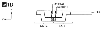
- an insulating layer, a first lower electrode formed on the insulating layer, and a second lower electrode formed on the insulating layer As an example of a structure that suppresses the occurrence of the crosstalk phenomenon of the light emitting device, an insulating layer, a first lower electrode formed on the insulating layer, and a second lower electrode formed on the insulating layer. , A structure formed on the insulating layer and located between the first lower electrode and the second lower electrode, and a structure formed on the insulating layer and the structure and the first lower electrode. A first partition located between the partition, a second partition formed on the insulating layer and located between the structure and the second lower electrode, the first lower electrode, and the first lower electrode. A first light emitting unit formed on the partition wall, the structure, the second partition wall and the second lower electrode, an intermediate layer formed on the first light emitting unit, and the intermediate layer.
- Patent Document 1 A structure including a second light emitting unit formed in the above and an upper electrode formed on the second light emitting unit is known (Pa
- One aspect of the present invention is to provide a novel functional panel having excellent convenience, usefulness, or reliability. Another issue is to provide a new display device having excellent convenience, usefulness, or reliability. Another issue is to provide a new input / output device having excellent convenience, usefulness, or reliability. Another issue is to provide a new information processing device having excellent convenience, usefulness, or reliability. Alternatively, one of the tasks is to provide a new function panel, a new display device, a new input / output device, a new information processing device, or a new semiconductor device.
- One aspect of the present invention is a functional panel having a first element, a first reflective film, and an insulating film.
- the first element comprises a first electrode, a second electrode and a layer containing a luminescent material, and the layer containing the luminescent material forms a region sandwiched between the first electrode and the second electrode. Be prepared.
- the first electrode is translucent and the first electrode has a first thickness. Further, the first reflective film has a region sandwiching the first electrode between the first reflective film and the layer containing the luminescent material, and the first reflective film has a second thickness.
- the insulating film has a first opening, the first opening overlaps the first electrode, the insulating film has a first stepped cross-sectional shape, and the first stepped cross-sectional shape is from above. Look around the first opening. Further, the first stepped cross-sectional shape includes the first step, and the first step is equal to or larger than the thickness obtained by adding the second thickness to the first thickness.
- the layer containing the luminescent material can be formed in the first step surrounding the first opening.
- the current flowing outside the first opening can be suppressed along the spread of the layer containing the luminescent material.
- the light emitting region can be concentrated in the region overlapping the first opening.
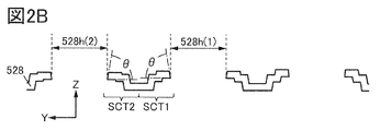
- the first stepped cross-sectional shape includes a second step and a third step between the first steps, and the second step is a third step.
- the above-mentioned functional panel which is smaller and has a second step of 0.5 times or more and 1.5 times or less of the first thickness.
- the second step can be changed according to the thickness of the first electrode.
- the third step can be made constant without being affected by the thickness of the first electrode.
- the layer containing the luminescent material can be thinned at the third step surrounding the first opening.
- the current flowing outside the first opening can be suppressed along the spread of the layer containing the luminescent material.
- the light emitting region can be concentrated in the region overlapping the first opening.
- one aspect of the present invention is the above-mentioned functional panel having a second element.
- the second element comprises a third electrode, a second electrode and a layer containing the luminescent material, the layer containing the luminescent material having a region sandwiched between the third electrode and the second electrode. Be prepared.
- the insulating film has a second opening, the second opening overlaps the third electrode, the insulating film has a second stepped cross section, and the second stepped cross section has a second step.
- the second stepped cross-sectional shape Surrounding the opening, the second stepped cross-sectional shape has an inclination, with an inclination of 60 ° or more and 90 ° or less with respect to the surface of the third electrode.
- a thin portion can be formed in the region surrounding the first opening and the region surrounding the second opening of the layer containing the luminescent material.
- the current flowing between the second electrode and the first electrode can be suppressed through the region overlapping the insulating film of the layer containing the luminescent material.
- the current flowing between the second electrode and the first electrode in the region overlapping the second opening can be suppressed through the region overlapping the insulating film of the layer containing the luminescent material.
- the current flowing between the second electrode and the third electrode in the region overlapping the first opening can be suppressed through the region overlapping the insulating film of the layer containing the luminescent material.
- the light emitting region can be concentrated in the region overlapping the first opening or the region overlapping the second opening.
- the influence of the operation of the first element on the operation of the second element can be suppressed.
- the second stepped cross-sectional shape includes a fourth step, and the fourth step is 0.7 times or more and 1.3 times or less of the first step. , The above functional panel.
- a thin portion of the layer containing the luminescent material can be formed in the first step surrounding the first opening and the second step surrounding the second opening.
- the current flowing between the second electrode and the first electrode can be suppressed through the region overlapping the insulating film of the layer containing the luminescent material.
- the current flowing between the second electrode and the first electrode in the region overlapping the second opening can be suppressed through the region overlapping the insulating film of the layer containing the luminescent material.
- the current flowing between the second electrode and the third electrode in the region overlapping the first opening can be suppressed through the region overlapping the insulating film of the layer containing the luminescent material.
- the light emitting region can be concentrated in the region overlapping the first opening or the region overlapping the second opening. As a result, it is possible to provide a new functional panel that is excellent in convenience, usefulness, or reliability.
- the third electrode has a fourth thickness
- the second stepped cross-sectional shape has a fifth step and a sixth step between the fourth steps.
- the fifth step is 0.5 times or more and 1.5 times or less of the fourth thickness, the fifth step is smaller than the sixth step, and the sixth step is 0.7 of the third step. It is more than double and 1.3 times or less.
- the second step can be changed according to the thickness of the third electrode.
- the third step and the sixth step can be made constant without being affected by the thickness of the first electrode and the thickness of the third electrode.
- a thin portion can be formed in the third step surrounding the first opening and the sixth step surrounding the second opening of the layer containing the luminescent material.
- the current flowing between the second electrode and the first electrode can be suppressed through the region overlapping the insulating film of the layer containing the luminescent material.
- the current flowing between the second electrode and the first electrode overlapping the second opening can be suppressed through the region overlapping the insulating film of the layer containing the luminescent material.
- the light emitting region can be concentrated in the region overlapping the first opening or the region overlapping the second opening. As a result, it is possible to provide a new functional panel that is excellent in convenience, usefulness, or reliability.
- one aspect of the present invention is the above-mentioned functional panel in which a layer containing a luminescent material includes a first light emitting unit, a second light emitting unit, and an intermediate layer.
- the first light emitting unit includes a region sandwiched between the first electrode and the intermediate layer. Further, the intermediate layer includes a region sandwiched between the first light emitting unit and the second light emitting unit, and the intermediate layer has higher conductivity than the second light emitting unit.
- a thin portion of the intermediate layer can be formed in the region surrounding the first opening of the layer containing the luminescent material.
- the current flowing outside the first opening can be suppressed along the spread of the layer containing the luminescent material.
- the light emitting region can be concentrated in the region overlapping the first opening.
- one aspect of the present invention is the above-mentioned functional panel having a set of pixels.
- a set of pixels comprises a first pixel and a second pixel, the first pixel comprises a first element and a pixel circuit, and the second pixel comprises a second element.
- the first element is electrically connected to the pixel circuit.
- the first element can be driven by using the pixel circuit.
- the display can be performed using the first pixel and the second pixel while preventing the occurrence of crosstalk.
- one aspect of the present invention is the above-mentioned functional panel having a functional layer.
- the functional layer comprises a pixel circuit, the pixel circuit comprises a first transistor, the functional layer comprises a drive circuit, and the drive circuit comprises a second transistor.
- the first transistor includes a semiconductor film
- the second transistor includes a semiconductor film that can be manufactured in the process of forming the semiconductor film.
- the pixel circuit can be formed in the functional layer.
- one aspect of the present invention has a region, and the region includes a set of pixels in a group, a set of pixels in another group, a first conductive film, and a second conductive film. It is a function panel of.
- a set of pixels in a group is arranged in the row direction, a set of pixels in a group includes the set of pixels described above, and a set of pixels in a group is electrically connected to a first conductive film.
- the other set of pixels is arranged in the column direction intersecting the row direction, the other set of pixels includes the above set of pixels, and the other set of pixels is the second. It is electrically connected to the conductive film of.
- image information can be supplied to a plurality of pixels.
- one aspect of the present invention is a display device having a control unit and the above-mentioned functional panel.
- the control unit is supplied with image information and control information, the control unit generates information based on the image information, the control unit generates a control signal based on the control information, and the control unit supplies the information and the control signal.
- the functional panel is supplied with information and control signals, and a set of pixels displays the information.
- image information can be displayed using the first element.
- one aspect of the present invention is an input / output device having an input unit and a display unit.
- the display unit includes the above-mentioned function panel, the input unit includes a detection area, the input unit detects an object close to the detection area, and the detection area includes an area overlapping the first pixel.
- the position information can be input by using a finger or the like close to the display unit as the pointer.
- the position information can be associated with the image information displayed on the display unit.
- one aspect of the present invention is an information processing device including an arithmetic unit and an input / output device.
- the arithmetic unit is supplied with input information or detection information, and the arithmetic unit generates control information and image information based on the input information or detection information.
- the arithmetic unit also supplies control information and image information.
- the input / output device supplies input information and detection information
- the input / output device is supplied with control information and image information
- the input / output device includes a display unit, an input unit, and a detection unit.
- the display unit includes the above-mentioned function panel, and the display unit displays image information based on the control information.
- the input unit generates input information
- the detection unit generates detection information.
- control information can be generated based on the input information or the detection information.
- the image information can be displayed based on the input information or the detection information.
- one aspect of the present invention includes one or more of a keyboard, a hardware button, a pointing device, a touch sensor, an illuminance sensor, an image pickup device, a voice input device, a line-of-sight input device, and an attitude detection device.
- An information processing device that includes a functional panel.
- the names of the source and drain of a transistor are interchanged depending on the polarity of the transistor and the level of potential given to each terminal.
- a terminal to which a low potential is given is called a source
- a terminal to which a high potential is given is called a drain.
- a terminal to which a low potential is given is called a drain
- a terminal to which a high potential is given is called a source.
- the connection relationship between transistors may be described on the assumption that the source and drain are fixed, but in reality, the names of source and drain are interchanged according to the above potential relationship. ..
- the source of a transistor means a source region that is a part of a semiconductor film that functions as an active layer, or a source electrode that is connected to the semiconductor film.
- the drain of a transistor means a drain region that is a part of the semiconductor membrane, or a drain electrode connected to the semiconductor membrane.
- the gate means a gate electrode.
- the state in which the transistors are connected in series means, for example, a state in which only one of the source or drain of the first transistor is connected to only one of the source or drain of the second transistor. To do. Further, in the state where the transistors are connected in parallel, one of the source or drain of the first transistor is connected to one of the source or drain of the second transistor, and the other of the source or drain of the first transistor is connected. It means the state of being connected to the source or the drain of the second transistor.
- connection means an electrical connection, and corresponds to a state in which a current, a voltage, or an electric potential can be supplied or transmitted. Therefore, the connected state does not necessarily mean the directly connected state, and the wiring, the resistor, the diode, the transistor, etc. so that the current, the voltage, or the potential can be supplied or transmitted.
- the state of being indirectly connected via a circuit element is also included in the category.
- one conductive film may be present in a plurality of cases, for example, when a part of the wiring functions as an electrode. In some cases, it also has the functions of the components of.
- connection includes the case where one conductive film has the functions of a plurality of components in combination.
- one of the first electrode or the second electrode of the transistor refers to the source electrode, and the other refers to the drain electrode.
- a novel functional panel having excellent convenience, usefulness or reliability.
- a new display device having excellent convenience, usefulness or reliability.
- a new input / output device having excellent convenience, usefulness, or reliability.
- a new information processing apparatus having excellent convenience, usefulness or reliability.
- a new functional panel, a new display device, a new input / output device, a new information processing device, or a new semiconductor device can be provided.
- FIG. 1A to 1D are diagrams for explaining the configuration of the functional panel according to the embodiment.
- 2A to 2D are diagrams for explaining the configuration of the functional panel according to the embodiment.
- FIG. 3 is a diagram for explaining the configuration of the functional panel according to the embodiment.
- 4A and 4B are diagrams illustrating the configuration of the functional panel according to the embodiment.
- 5A to 5C are diagrams for explaining the configuration of the functional panel according to the embodiment.
- FIG. 6 is a circuit diagram illustrating the configuration of the functional panel according to the embodiment.
- FIG. 7 is a circuit diagram illustrating the configuration of the functional panel according to the embodiment.
- 8A and 8B are circuit diagrams illustrating the configuration of the functional panel according to the embodiment.
- FIG. 9 is a cross-sectional view illustrating the configuration of the functional panel according to the embodiment.
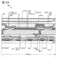
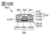
- FIG. 10A and 10B are cross-sectional views illustrating the configuration of the functional panel according to the embodiment.
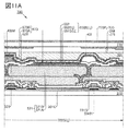
- 11A and 11B are cross-sectional views illustrating the configuration of the functional panel according to the embodiment.
- 12A and 12B are cross-sectional views illustrating the configuration of the functional panel according to the embodiment.
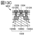
- 13A to 13C are cross-sectional views illustrating the configuration of the functional panel according to the embodiment.
- 14A and 14B are diagrams illustrating the configuration of the functional panel according to the embodiment.
- FIG. 15 is a diagram illustrating the operation of the functional panel according to the embodiment.
- 16A to 16D are diagrams for explaining the configuration of the display device according to the embodiment.
- FIG. 17 is a block diagram illustrating the configuration of the input / output device according to the embodiment.
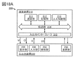
- 18A to 18C are block diagrams and projection views for explaining the configuration of the information processing apparatus according to the embodiment.
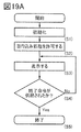
- 19A and 19B are flowcharts illustrating a method of driving the information processing apparatus according to the embodiment.
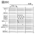
- 20A to 20C are diagrams for explaining the driving method of the information processing apparatus according to the embodiment.
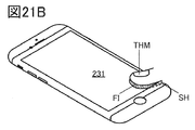
- 21A to 21C are diagrams for explaining a method of driving the information processing apparatus according to the embodiment.
- 22A to 22D are diagrams for explaining the driving method of the information processing apparatus according to the embodiment.
- 23A to 23E are diagrams for explaining the configuration of the information processing apparatus according to the embodiment.
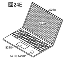
- 24A to 24E are diagrams for explaining the configuration of the information processing apparatus according to the embodiment.
- 25A and 25B are diagrams for explaining the configuration of the information processing apparatus according to the embodiment.
- 26A is a top view of a semiconductor device according to an aspect of the present invention.
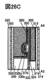
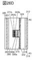
- 26B to 26D are cross-sectional views of a semiconductor device according to an aspect of the present invention.
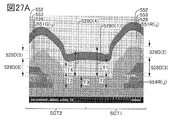
- 27A and 27B are transmission electron micrographs illustrating a cross section of a functional panel according to an embodiment.
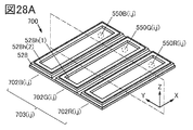
- 28A to 28C are diagrams for explaining the configuration and characteristics of the functional panel according to the embodiment.
- 29A and 29B are diagrams illustrating the configuration of the functional panel according to the embodiment.
- FIG. 30A is a diagram for explaining a method for manufacturing the functional panel according to the embodiment
- FIG. 30B is a diagram for explaining the characteristics of the colored film of the functional panel according to the embodiment.
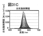
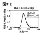
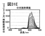
- 31A to 31F are diagrams for explaining the characteristics of the functional panel according to the embodiment.
- FIG. 32A to 32F are diagrams for explaining the characteristics of the functional panel according to the embodiment.
- 33A and 33B are photographs of the functional panel according to the embodiment
- FIG. 33C is a diagram illustrating the characteristics of the functional panel according to the embodiment.
- FIG. 34 is a diagram illustrating a configuration of a light emitting element according to an embodiment.
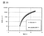
- FIG. 35 is a diagram for explaining the voltage-luminance characteristic of the light emitting element according to the embodiment.
- FIG. 36 is a diagram illustrating an emission spectrum when the light emitting element according to the embodiment is made to emit light at a brightness of 1000 cd / m 2.
- FIG. 37 is a diagram illustrating a voltage-luminance characteristic of the comparative light emitting device according to the embodiment.
- FIG. 38 is a diagram illustrating an emission spectrum when the comparative light emitting device according to the embodiment is made to emit light at a brightness of 1000 cd / m 2.
- the functional panel of one aspect of the present invention includes a first element, a first reflective film, and an insulating film.
- the first element comprises a first electrode, a second electrode and a layer containing a luminescent material, and the layer containing the luminescent material comprises a region sandwiched between the first electrode and the second electrode.
- the first electrode has a translucent property, the first electrode has a first thickness, and the first reflective film has a region sandwiching the first electrode with a layer containing a luminescent material.
- the first reflective film has a second thickness.
- the insulating film has a first opening, the first opening overlaps the first electrode, the insulating film has a first stepped cross-sectional shape, and the first stepped cross-sectional shape is the first. The step is provided, and the first step is equal to or larger than the thickness obtained by adding the second thickness to the first thickness.
- a thin portion can be formed in the region surrounding the first opening 528h (1) of the layer 553 containing the luminescent material.
- the current flowing outside the first opening 528h (1) can be suppressed along the spread of the layer 553 containing the luminescent material.
- the light emitting region can be concentrated in the region overlapping the first opening 528h (1).
- FIG. 1A is a perspective view of a functional panel according to an aspect of the present invention
- FIG. 1B is a cross-sectional view taken along the cut surface YY of FIG. 1A
- FIGS. 1C and 1D are diagrams for explaining a part of FIG. 1B.
- FIG. 2A is a perspective view of a functional panel according to an aspect of the present invention
- FIG. 2B is a cross-sectional view taken along the cut surface YY of FIG. 2A
- 2C and 2D are diagrams illustrating a part of FIG. 2B.
- FIG. 3 is a diagram illustrating a part of FIG. 1C.
- a variable having an integer of 1 or more as a value may be used as a code.
- (p) containing a variable p having a value of one or more integers may be used as a part of a code for specifying any of the maximum p components.
- (m, n) including a variable m having a value of one or more integers and a variable n may be used as a part of a code for specifying any of a maximum of m ⁇ n components.
- the functional panel described in this embodiment includes an element 550G (i, j), a reflective film 554G (i, j), and an insulating film 528 (see FIG. 1C).
- the element 550G (i, j) includes an electrode 551G (i, j), an electrode 552, and a layer 553 containing a luminescent material.
- the layer 553 containing the luminescent material comprises a region sandwiched between the electrodes 551G (i, j) and the electrodes 552.
- the electrode 551G (i, j) is translucent, and the electrode 551G (i, j) has a thickness T1.
- the thickness T1 can be controlled to adjust the distance between the layer 553 containing the luminescent material and the reflective film 554G (i, j).
- a microcavity structure can be formed on the functional panel 700.
- light having a specific wavelength can be efficiently extracted from the element 550G (i, j).
- the reflective film 554G (i, j) includes a region sandwiching the electrode 551G (i, j) between the reflective film 554G (i, j) and the layer 553 containing the luminescent material, and the reflective film 554G (i, j) has a thickness T2.
- a conductive material can be used for the reflective film 554G (i, j).
- wiring or the like can be used for the reflective film 554G (i, j).
- the insulating film 528 has a thickness T3, and the thickness T3 is equal to or greater than the thickness T1 plus the thickness T2. Further, the insulating film 528 includes an opening 528h (1) (see FIGS. 1A to 1C).
- the opening 528h (1) overlaps the electrode 551G (i, j), and the insulating film 528 has a stepped cross-sectional shape SCT1 (see FIGS. 1C and 1D).
- the stepped cross-sectional shape SCT1 surrounds the opening 528h (1), and the stepped cross-sectional shape SCT1 has an inclination ⁇ (see FIGS. 1A and 1B).
- the inclination ⁇ is 60 ° or more and 90 ° or less with respect to the surface of the electrode 551G (i, j) (see FIG. 1C). Specifically, the inclination ⁇ is an angle with respect to the surface where the electrode 551G (i, j) is in contact with the layer 553 containing the luminescent material. Alternatively, the inclination ⁇ is the angle of the side surface of the insulating film 528 with respect to the bottom surface. The thickness of the layer 553 containing the luminescent material is thinner in the region in contact with the side surface of the insulating film 528 having the inclination ⁇ than in the region in contact with the electrodes 551G (i, j).
- a thin portion can be formed in the region surrounding the opening 528h (1) of the layer 553 containing the luminescent material.
- the current flowing outside the opening 528h (1) can be suppressed along the spread of the layer 553 containing the luminescent material.
- the light emitting region can be concentrated in the region overlapping the opening 528h (1).
- the stepped cross-sectional shape SCT1 includes a step 528D (1) (see FIGS. 1C and 1D).
- the step 528D (1) is equal to or larger than the thickness T1 plus the thickness T2.
- a step 528D (step 528D) is formed on the insulating film 528. 1) can be formed.
- the step 528D (1) having the same thickness as the thickness T1 plus the thickness T2 can be formed.
- the insulating film 528 can be formed on the processed member in which the insulating film 522G, the reflective film 554G (i, j) having a thickness T2, and the electrode 551G (i, j) having a thickness T1 are laminated. Thereby, a larger step can be formed.
- a thin portion of the layer 553 containing the luminescent material can be formed in the step 528D (1) surrounding the opening 528h (1).
- the current flowing outside the opening 528h (1) can be suppressed along the spread of the layer 553 containing the luminescent material.
- the light emitting region can be concentrated in the region overlapping the opening 528h (1).
- the stepped cross-sectional shape SCT1 includes a step 528D (2) and a step 528D (3) between the steps 528D (1) (see FIGS. 2C and 2D).
- the step 528D (2) is smaller than the step 528D (3), and the step 528D (2) is 0.5 times or more and 1.5 times or less the thickness T1.
- the step 528D (2) has a step having the same thickness as T1.
- the step 528D (3) is not affected by the thickness T1 of the electrode 551G (i, j).
- the step 528D (2) can be changed according to the thickness T1 of the electrode 551G (i, j).
- the step 528D (3) can be made constant without being affected by the thickness T1 of the electrode 551G (i, j).
- the layer 553 containing the luminescent material can be thinned at the step 528D (3) surrounding the opening 528h (1).
- the current flowing outside the opening 528h (1) can be suppressed along the spread of the layer 553 containing the luminescent material.
- the light emitting region can be concentrated in the region overlapping the opening 528h (1). As a result, it is possible to provide a new functional panel that is excellent in convenience, usefulness, or reliability.
- the functional panel described in this embodiment has elements 550B (i, j) (see FIGS. 1A, 1C, 2A and 2C).
- the element 550B (i, j) comprises a layer 553 containing an electrode 551B (i, j), an electrode 552, and a luminescent material (see FIGS. 1C and 2C).
- the layer 553 containing the luminescent material comprises a region sandwiched between the electrodes 551B (i, j) and the electrodes 552.
- the insulating film 528 includes an opening 528h (2) (see FIGS. 1A, 1B, 2A and 2B). Further, the opening 528h (2) overlaps with the electrode 551B (i, j), and the insulating film 528 has a stepped cross-sectional shape SCT2.
- the stepped cross-sectional shape SCT2 surrounds the opening 528h (2), and the stepped cross-sectional shape SCT2 has an inclination ⁇ (see FIGS. 1C and 2C).
- the inclination ⁇ is 60 ° or more and 90 ° or less with respect to the surface of the electrode 551B (i, j).
- a thin portion can be formed in the region surrounding the opening 528h (1) and the region surrounding the opening 528h (2) in the layer 553 containing the luminescent material.
- the current flowing between the electrode 552 and the electrode 551G (i, j) in the region overlapping the opening 528h (2) is suppressed through the region overlapping the insulating film 528 of the layer 553 containing the luminescent material.
- the current flowing between the electrode 552 and the electrode 551B (i, j) in the region overlapping the opening 528h (1) is suppressed through the region overlapping the insulating film 528 of the layer 553 containing the luminescent material. Can be done.
- the light emitting region can be concentrated in the region overlapping the opening 528h (1) or the region overlapping the opening 528h (2).
- the influence of the operation of the element 550G (i, j) on the operation of the element 550B (i, j) can be suppressed.
- a new functional panel that is excellent in convenience, usefulness, or reliability.
- the stepped cross-sectional shape SCT2 includes a step 528D (4), and the step 528D (4) is 0.7 times or more and 1.3 times or less, preferably 0.9 times or more and 1.1 times the step 528D (1).
- the insulating film 528 can be formed on a processed member in which the insulating film 522B, the reflective film 554B (i, j) having a thickness T2, and the electrode 551B (i, j) having a thickness T4 are laminated.
- the step 528D (4) can be made about the same as the step 528D (1).
- the thickness of the insulating film 522B can be adjusted so that the step 528D (4) is about the same as the step 528D (1).
- a thin portion of the layer 553 containing the luminescent material is formed on the step 528D (1) surrounding the opening 528h (1) and the step 528D (4) surrounding the opening 528h (2).
- the current flowing between the electrode 552 and the electrode 551G (i, j) in the region overlapping the opening 528h (2) is suppressed through the region overlapping the insulating film 528 of the layer 553 containing the luminescent material.
- the current flowing between the electrode 552 and the electrode 551B (i, j) in the region overlapping the opening 528h (1) is suppressed through the region overlapping the insulating film 528 of the layer 553 containing the luminescent material.
- the light emitting region can be concentrated in the region overlapping the opening 528h (1) or the region overlapping the opening 528h (2). As a result, it is possible to provide a new functional panel that is excellent in convenience, usefulness, or reliability.
- Electrodes 551B (i, j) have a thickness T4 (see FIG. 2C).
- the stepped cross-sectional shape SCT2 includes a step 528D (5) and a step 528D (6) between the steps 528D (4) (see FIGS. 2C and 2D).
- the step 528D (5) is 0.5 times or more and 1.5 times or less the thickness T4, and the step 528D (5) is smaller than the step 528D (6).
- the step 528D (6) is 0.7 times or more, 1.3 times or less, preferably 0.9 times or more and 1.1 times or less the step 528D (3).
- the step 528D (5) has a step similar to the thickness T4.
- the step 528D (6) is not affected by the thickness T4 of the electrode 551B (i, j).
- the step 528D (5) can be changed according to the thickness T4 of the electrode 551B (i, j).
- the step 528D (3) and the step 528D (6) can be made constant without being affected by the thickness T1 of the electrode 551G (i, j) and the thickness T4 of the electrode 551B (i, j). ..
- a thin portion is formed on the step 528D (3) surrounding the opening 528h (1) and the step 528D (6) surrounding the opening 528h (2) of the layer 553 containing the luminescent material. Can be done.
- the current flowing between the electrode 552 and the electrode 551G (i, j) overlapping the opening 528h (2) can be suppressed through the region overlapping the insulating film 528 of the layer 553 containing the luminescent material. ..
- the current flowing between the electrode 552 and the electrode 551B (i, j) overlapping the opening 528h (1) can be suppressed through the region overlapping the insulating film 528 of the layer 553 containing the luminescent material. ..
- the light emitting region can be concentrated in the region overlapping the opening 528h (1) or the region overlapping the opening 528h (2). As a result, it is possible to provide a new functional panel that is excellent in convenience, usefulness, or reliability.
- the layer 553 containing the luminescent material includes a light emitting unit 103 (1), a light emitting unit 103 (2), and an intermediate layer 106 (see FIG. 3).
- the light emitting unit 103 (1) is sandwiched between the electrodes 551G (i, j) and the intermediate layer 106.
- the light emitting unit includes one region in which an electron injected from one side recombines with a hole injected from the other side.
- the light emitting unit includes a light emitting material, and the light emitting material emits energy generated by recombination of electrons and holes as light.
- a configuration that emits blue light can be used for the light emitting unit 103 (1), and a configuration that emits yellow light can be used for the light emitting unit 103 (2).
- the layer 553 containing the luminescent material can be configured to emit white light.
- the intermediate layer 106 includes a region sandwiched between the light emitting unit 103 (1) and the light emitting unit 103 (2), and the intermediate layer 106 has higher conductivity than the light emitting unit 103 (2).
- the intermediate layer comprises a region sandwiched between the two light emitting units.
- the intermediate layer has a charge generation region, and the intermediate layer has a function of supplying holes to a light emitting unit arranged on the cathode side and supplying electrons to a light emitting unit arranged on the anode side.
- a configuration including a plurality of light emitting units and an intermediate layer may be referred to as a tandem type light emitting element.
- the thin portion 106N of the intermediate layer 106 can be formed in the region surrounding the opening 528h (1) of the layer 553 containing the luminescent material.
- the current flowing outside the opening 528h (1) can be suppressed along the spread of the layer 553 containing the luminescent material.
- the light emitting region can be concentrated in the region overlapping the opening 528h (1).
- FIG. 4A is a top view illustrating the configuration of the functional panel according to one aspect of the present invention
- FIG. 4B is a diagram illustrating a part of FIG. 4A.
- FIG. 5A is a diagram for explaining a part of FIG. 4A
- FIG. 5B is a diagram for explaining a part of FIG. 5A
- FIG. 5C is a diagram for explaining another part of FIG. 5A.
- FIG. 6 is a circuit diagram illustrating a configuration of a pixel circuit that can be used in the functional panel of one aspect of the present invention.
- FIG. 7 is a circuit diagram illustrating a configuration of a pixel circuit that can be used in the functional panel of one aspect of the present invention.
- FIG. 8A is a circuit diagram illustrating a part of an amplifier circuit that can be used for the functional panel of one aspect of the present invention
- FIG. 8B is a circuit diagram of a sampling circuit that can be used for the functional panel of one aspect of the present invention. Is.
- the functional panel 700 has a set of pixels 703 (i, j) (see FIG. 4A).
- the functional panel 700 includes the conductive film G1 (i), the conductive film G2 (i), the conductive film S1g (j), the conductive film S2g (j), the conductive film ANO, the conductive film VCOM2, and the conductive film. It has V0 (see FIG. 6).
- the conductive film G1 (i) is supplied with a first selection signal
- the conductive film G2 (i) is supplied with a second selection signal
- the conductive film S1g (j) is supplied with an image signal to be conductive.
- the film S2g (j) is supplied with a control signal.
- a set of pixels 703 (i, j) includes pixels 702G (i, j) (see FIG. 4B).
- the pixel 702G (i, j) includes a pixel circuit 530G (i, j) and an element 550G (i, j) (see FIG. 5A).
- ⁇ Configuration Example 1 of Pixel Circuit 530G (i, j) The pixel circuit 530G (i, j) is supplied with the first selection signal, and the pixel circuit 530G (i, j) acquires an image signal based on the first selection signal.
- the conductive film G1 (i) can be used to supply the first selection signal (see FIG. 5B).
- the image signal can be supplied using the conductive film S1g (j).
- the operation of supplying the first selection signal and causing the pixel circuit 530G (i, j) to acquire the image signal can be referred to as “writing” (see FIG. 15).
- the pixel circuit 530G (i, j) includes a switch SW21, a switch SW22, a transistor M21, a capacitance C21, and a node N21 (see FIG. 6). Further, the pixel circuit 530G (i, j) includes a node N22, a capacitance C22, and a switch SW23.
- the transistor M21 has a gate electrode electrically connected to the node N21, a first electrode electrically connected to the element 550G (i, j), and a second electrode electrically connected to the conductive film ANO. It is equipped with an electrode.
- the switch SW21 is based on the potential of the first terminal electrically connected to the node N21, the second terminal electrically connected to the conductive film S1g (j), and the conductive film G1 (i). It has a function to control the conducting state or the non-conducting state.
- the switch SW22 has a first terminal electrically connected to the conductive film S2g (j) and a function of controlling a conductive state or a non-conductive state based on the potential of the conductive film G2 (i).
- the capacitance C21 includes a conductive film that is electrically connected to the node N21 and a conductive film that is electrically connected to the second electrode of the switch SW22.
- the image signal can be stored in the node N21.
- the potential of the node N21 can be changed using the switch SW22.
- the intensity of the light emitted by the element 550G (i, j) can be controlled by using the potential of the node N21. As a result, it is possible to provide a new function panel having excellent convenience or reliability.
- the element 550G (i, j) is electrically connected to the pixel circuit 530G (i, j) (see FIG. 5A). Further, the element 550G (i, j) includes an electrode 551G (i, j) electrically connected to the pixel circuit 530G (i, j) and an electrode 552 electrically connected to the conductive film VCOM2 ( 6 and 10A). The element 550G (i, j) has a function of operating based on the potential of the node N21.
- an organic electroluminescence element for example, an organic electroluminescence element, an inorganic electroluminescence element, a light emitting diode, a QDLED (Quantum Dot LED), or the like can be used for the element 550G (i, j).
- a QDLED Quantum Dot LED
- the functional panels described in this embodiment include the conductive film RS (i), the conductive film TX (i), the conductive film SE (i), the conductive film VR, the conductive film VCP, and the conductive film VPI. It has a conductive film WX (j) (see FIG. 7).
- the conductive film RS (i) is supplied with a third selection signal
- the conductive film TX (i) is supplied with a fourth selection signal
- the conductive film SE (i) is supplied with a fifth selection signal. ..
- Pixel 703 (i, j) includes pixel 702S (i, j) (see FIG. 4B).
- Pixel 702S (i, j) includes pixel circuit 530S (i, j) and element 550S (i, j) (see FIG. 5A).
- the pixel circuit 530S (i, j) includes a switch SW31, a switch SW32, a switch SW33, a transistor M31, a capacitance C31, and a node FD (see FIG. 7).
- the switch SW31 is based on the potential of the first terminal electrically connected to the element 550S (i, j), the second terminal electrically connected to the node FD, and the conductive film TX (i). , It has a function to control a conductive state or a non-conducting state.
- the switch SW32 is in a conductive state or is based on the potential of the first terminal electrically connected to the node FD, the second terminal electrically connected to the conductive film VR, and the conductive film RS (i). It has a function to control the non-conducting state.
- the capacitance C31 includes a conductive film that is electrically connected to the node FD and a conductive film that is electrically connected to the conductive film VCP.
- the transistor M31 includes a gate electrode electrically connected to the node FD and a first electrode electrically connected to the conductive film VPI.
- the switch SW33 is of the first terminal electrically connected to the second electrode of the transistor M31, the second terminal electrically connected to the conductive film WX (j), and the conductive film SE (i). It has a function of controlling a conducting state or a non-conducting state based on a potential.
- the image pickup signal generated by the element 550S (i, j) can be transferred to the node FD by using the switch SW31.
- the image pickup signal generated by the element 550S (i, j) can be stored in the node FD by using the switch SW31.
- the switch SW31 can be used to bring the pixel circuit 530S (i, j) and the element 550S (i, j) into a non-conducting state.
- the correlated double sampling method can be applied.
- the noise included in the image pickup signal can be reduced. As a result, it is possible to provide a new function panel having excellent convenience or reliability.
- the element 550S (i, j) is electrically connected to the pixel circuit 530S (i, j) (see FIG. 5A).
- the element 550S (i, j) has a function of generating an imaging signal.
- a heterojunction type photoelectric conversion element, a bulk heterojunction type photoelectric conversion element, or the like can be used for the element 550S (i, j).
- a plurality of pixels can be used for the pixel 703 (i, j). For example, it is possible to use a plurality of pixels that display colors having different hues from each other. It should be noted that each of the plurality of pixels can be paraphrased as a sub-pixel. Alternatively, a plurality of sub-pixels can be combined into a set and can be paraphrased as a pixel.
- the colors displayed by the plurality of pixels can be additively mixed or subtracted.
- pixels 702B (i, j) for displaying blue, pixels 702G (i, j) for displaying green, and pixels 702R (i, j) for displaying red are used for pixels 703 (i, j). be able to. Further, each of the pixels 702B (i, j), the pixels 702G (i, j) and the pixels 702R (i, j) can be paraphrased as sub-pixels (see FIG. 4B).
- a pixel displaying white or the like can be used for the pixel 703 (i, j) in addition to the above set.
- a pixel for displaying cyan, a pixel for displaying magenta, and a pixel for displaying yellow can be used for the pixel 703 (i, j).
- a pixel that emits infrared rays can be used for the pixel 703 (i, j) in addition to the above set.
- a pixel that emits light including light having a wavelength of 650 nm or more and 1000 nm or less can be used for the pixel 703 (i, j).
- the functional panel described in this embodiment includes a drive circuit GD, a drive circuit SD, and a drive circuit RD (see FIG. 4A).
- the drive circuit GD has a function of supplying a first selection signal and a second selection signal.
- the drive circuit GD is electrically connected to the conductive film G1 (i) to supply a first selection signal, and is electrically connected to the conductive film G2 (i) to supply a second selection signal.
- the drive circuit SD has a function of supplying an image signal and a control signal, and the control signal includes a first level and a second level.
- the drive circuit SD is electrically connected to the conductive film S1g (j) to supply an image signal, and is electrically connected to the conductive film S2g (j) to supply a control signal.
- the drive circuit RD has a function of supplying a third selection signal to a fifth selection signal.
- the drive circuit RD is electrically connected to the conductive film RS (i) to supply a third selection signal, and is electrically connected to the conductive film TX (i) to supply a fourth selection signal. It is electrically connected to the conductive film SE (i) and supplies a fifth selection signal.
- the functional panel described in this embodiment has a conductive film VLEN, a conductive film VIV, and a readout circuit RC (see FIGS. 8A, 8B, and 4A).
- the read-out circuit RC includes a read-out circuit RC (j).
- the functional panel has a conductive film CDS VDD, a conductive film CDSVSS, a conductive film CDSBIAS, a conductive film CAPSEL, and a conductive film VCL.
- the readout circuit RC (j) includes an amplifier circuit and a sampling circuit SC (j) (see FIGS. 8A and 8B).
- the amplifier circuit includes a transistor M32 (j) (see FIG. 8A).
- the transistor M32 (j) has a gate electrode electrically connected to the conductive film VLEN, a first electrode electrically connected to the conductive film WX (j), and a first electrode electrically connected to the conductive film VIV. It is provided with two electrodes.
- the conductive film WX (j) connects the transistor M31 and the transistor M32 (see FIGS. 7 and 8A).
- the source follower circuit can be configured by using the transistor M31 and the transistor M32.
- the potential of the conductive film WX (j) can be changed based on the potential of the node FD.
- the sampling circuit SC (j) includes a first terminal IN (j), a second terminal, and a third terminal OUT (j) (see FIG. 8B). It also has a node NS.
- the first terminal IN (j) is electrically connected to the conductive film WX (j), the second terminal is electrically connected to the conductive film CL, and the third terminal OUT (j) is the first terminal. It has a function of supplying a signal that changes based on the potential of IN (j).
- the image pickup signal can be acquired from the pixel circuit 530S (i, j).
- a correlated double sampling method can be applied.
- the difference signal of the pixel circuit 530S (i, j) can be acquired for each conductive film WX (j).
- noise can be reduced.
- FIG. 9 is a diagram illustrating a configuration of a functional panel according to one aspect of the present invention, in which the cutting lines X1-X2, X3-X4, X9-X10, X11-X12 and a set of pixels 703 (i, j) of FIG. 4A are shown. ) Is a cross-sectional view.
- FIG. 10A is a diagram illustrating a configuration of a functional panel according to one aspect of the present invention, and is a cross-sectional view of pixels 702G (i, j) shown in FIG. 4B.
- FIG. 10B is a cross-sectional view illustrating a part of FIG. 10A.
- FIG. 11A is a diagram illustrating a configuration of a functional panel according to one aspect of the present invention, and is a cross-sectional view of pixels 702S (i, j) shown in FIG. 4B.
- 11B is a cross-sectional view illustrating a part of FIG. 11A.
- FIG. 12A is a diagram illustrating a configuration of a functional panel according to one aspect of the present invention, and is a cross-sectional view taken along the cutting lines X1-X2 and cutting lines X3-X4 of FIG. 4A.
- FIG. 12B is a diagram illustrating a part of FIG. 12A.
- the functional panel described in this embodiment has a functional layer 520 (see FIG. 9).
- the functional layer 520 includes a pixel circuit 530G (i, j) (see FIG. 9).
- the functional layer 520 includes, for example, the transistor M21 used in the pixel circuit 530G (i, j) (see FIGS. 4 and 10A).
- the functional layer 520 includes an opening 591G.
- the pixel circuit 530G (i, j) is electrically connected to the element 550G (i, j) at the opening 591G (see FIGS. 9 and 10A).
- the functional layer 520 includes a pixel circuit 530S (i, j) (see FIG. 9).
- the functional layer 520 includes, for example, a transistor used for the switch SW31 of the pixel circuit 530S (i, j) (see FIGS. 9 and 11A).
- the functional layer 520 includes an opening 591S, and the pixel circuit 530S (i, j) is electrically connected to the element 550S (i, j) at the opening 591S (see FIGS. 9 and 11A).
- the pixel circuit 530G (i, j) can be formed on the functional layer 520.
- the pixel circuit 530S (i, j) can be formed on the functional layer 520.
- the semiconductor film used for the pixel circuit 530G (i, j) can be formed in the step of forming the semiconductor film used for the pixel circuit 530G (i, j).
- the manufacturing process can be simplified. As a result, it is possible to provide a new functional panel that is excellent in convenience, usefulness, or reliability.
- the functional layer 520 includes a drive circuit GD (see FIGS. 4A and 9).
- the functional layer 520 includes, for example, a transistor MD used in the drive circuit GD (see FIGS. 9 and 12A).
- the functional layer 520 includes a drive circuit RD and a read circuit RC (see FIG. 9).
- the semiconductor film used for the drive circuit GD can be formed.
- the semiconductor film used for the drive circuit RD and the readout circuit RC can be formed.
- the manufacturing process of the functional panel can be simplified. As a result, it is possible to provide a new functional panel that is excellent in convenience, usefulness, or reliability.
- Transistor configuration example It can be used for the functional layer 520 such as a bottom gate type transistor or a top gate type transistor. Specifically, a transistor can be used as a switch.
- the transistor includes a semiconductor film 508, a conductive film 504, a conductive film 512A and a conductive film 512B (see FIG. 10B).
- the semiconductor film 508 includes a region 508A electrically connected to the conductive film 512A and a region 508B electrically connected to the conductive film 512B.
- the semiconductor film 508 includes a region 508C between the regions 508A and 508B.
- the conductive film 504 includes a region overlapping the region 508C, and the conductive film 504 has a function of a gate electrode.
- the insulating film 506 includes a region sandwiched between the semiconductor film 508 and the conductive film 504.
- the insulating film 506 has the function of a gate insulating film.
- the conductive film 512A has one of the functions of the source electrode and the function of the drain electrode, and the conductive film 512B has the function of the source electrode or the function of the drain electrode.
- the conductive film 524 can be used for the transistor.
- the conductive film 524 includes a region sandwiching the semiconductor film 508 with the conductive film 504.
- the conductive film 524 has the function of a second gate electrode.
- the semiconductor film used for the transistor of the drive circuit can be formed.
- a semiconductor film having the same composition as the semiconductor film used for the transistor of the pixel circuit can be used for the drive circuit.
- a semiconductor containing a Group 14 element can be used for the semiconductor film 508.
- a semiconductor containing silicon can be used for the semiconductor film 508.
- Hydroated amorphous silicon can be used for the semiconductor film 508.
- microcrystalline silicon or the like can be used for the semiconductor film 508. Thereby, for example, it is possible to provide a functional panel having less display unevenness than a functional panel using polysilicon for the semiconductor film 508. Alternatively, it is easy to increase the size of the functional panel.
- polysilicon can be used for the semiconductor film 508.
- the electric field effect mobility of the transistor can be made higher than that of the transistor using hydride amorphous silicon for the semiconductor film 508.
- the driving ability can be enhanced as compared with a transistor using hydrogenated amorphous silicon for the semiconductor film 508.
- the aperture ratio of the pixel can be improved as compared with a transistor using hydride amorphous silicon for the semiconductor film 508.
- the reliability of the transistor can be improved as compared with a transistor using hydride amorphous silicon for the semiconductor film 508.
- the temperature required for manufacturing the transistor can be made lower than that of a transistor using, for example, single crystal silicon.
- the semiconductor film used for the transistor of the drive circuit can be formed by the same process as the semiconductor film used for the transistor of the pixel circuit.
- the drive circuit can be formed on the same substrate as the substrate on which the pixel circuit is formed. Alternatively, the number of parts constituting the electronic device can be reduced.
- single crystal silicon can be used for the semiconductor film 508.
- the definition can be improved as compared with the functional panel in which hydrogenated amorphous silicon is used for the semiconductor film 508.
- a smart glass or head-mounted display can be provided.
- a metal oxide can be used for the semiconductor film 508.
- the time during which the pixel circuit can hold the image signal can be lengthened as compared with the pixel circuit using the transistor using amorphous silicon as the semiconductor film.
- the selection signal can be supplied at a frequency of less than 30 Hz, preferably less than 1 Hz, more preferably less than once a minute, while suppressing the occurrence of flicker.
- the fatigue accumulated in the user of the information processing apparatus can be reduced.
- the power consumption associated with driving can be reduced.
- the time during which the pixel circuit can hold an image pickup signal can be lengthened.
- the second selection signal can be supplied at a frequency of less than 30 Hz, preferably less than 1 Hz, more preferably less than once a minute.
- a transistor using an oxide semiconductor can be used.
- an oxide semiconductor containing indium, an oxide semiconductor containing indium, gallium and zinc, or an oxide semiconductor containing indium, gallium, zinc and tin can be used for the semiconductor film.
- a transistor whose leakage current in the off state is smaller than that of a transistor using amorphous silicon for the semiconductor film can be used.
- a transistor using an oxide semiconductor as a semiconductor film can be used for a switch or the like.
- the potential of the floating node can be maintained for a longer time than in a circuit using a transistor using amorphous silicon as a switch.
- a film having a thickness of 25 nm containing indium, gallium, and zinc can be used for the semiconductor film 508.
- a conductive film in which a film having a thickness of 10 nm containing tantalum and nitrogen and a film having a thickness of 300 nm containing copper is laminated can be used for the conductive film 504.
- the copper-containing film includes a region sandwiching the tantalum and nitrogen-containing film between the copper-containing film and the insulating film 506.
- a laminated film in which a film having a thickness of 400 nm containing silicon and nitrogen and a film having a thickness of 200 nm containing silicon, oxygen and nitrogen are laminated can be used as the insulating film 506.
- the film containing silicon and nitrogen includes a region sandwiching the film containing silicon, oxygen and nitrogen between the film and the semiconductor film 508.
- a conductive film in which a film having a thickness of 50 nm containing tungsten, a film having a thickness of 400 nm containing aluminum, and a film having a thickness of 100 nm containing titanium are laminated in this order is formed on the conductive film 512A or 512B.
- the film containing tungsten includes a region in contact with the semiconductor film 508.
- a bottom gate type transistor manufacturing line using amorphous silicon for a semiconductor can be easily modified into a bottom gate type transistor manufacturing line using an oxide semiconductor for a semiconductor.
- a top gate type transistor manufacturing line using polysilicon as a semiconductor can be easily modified into a top gate type transistor manufacturing line using an oxide semiconductor as a semiconductor. Both modifications can make effective use of the existing production line.
- a compound semiconductor can be used as a semiconductor of a transistor.
- a semiconductor containing gallium arsenide can be used.
- an organic semiconductor can be used as a semiconductor of a transistor.
- an organic semiconductor containing polyacenes or graphene can be used for the semiconductor film.
- the capacitance includes one conductive film, another conductive film and an insulating film.
- the insulating film includes a region sandwiched between one conductive film and another conductive film.
- a conductive film used for the source electrode or drain electrode of the transistor, a conductive film used for the gate electrode, and an insulating film used for the gate insulating film can be used for the capacitance.
- the functional layer 520 includes an insulating film 521, an insulating film 518, an insulating film 516, an insulating film 506, an insulating film 501C, and the like (see FIGS. 10A and 10B).
- the insulating film 521 includes a region sandwiched between the pixel circuit 530G (i, j) and the element 550G (i, j).
- the insulating film 518 includes a region sandwiched between the insulating film 521 and the insulating film 501C.
- the insulating film 516 includes a region sandwiched between the insulating film 518 and the insulating film 501C.
- the insulating film 506 includes a region sandwiched between the insulating film 516 and the insulating film 501C.
- Insulating film 521 A film obtained by laminating the insulating film 521A and the insulating film 521B can be used as the insulating film 521.
- an insulating inorganic material, an insulating organic material, or an insulating composite material containing the inorganic material and the organic material can be used for the insulating film 521.
- an inorganic oxide film, an inorganic nitride film, an inorganic nitride film, or a laminated material obtained by laminating a plurality of selected materials thereof can be used for the insulating film 521.
- a silicon oxide film, a silicon nitride film, a silicon nitride film, an aluminum oxide film, or a film containing a laminated material selected from these can be used as the insulating film 521.
- the silicon nitride film is a dense film and has an excellent function of suppressing the diffusion of impurities.
- polyester, polyolefin, polyamide, polyimide, polycarbonate, polysiloxane, acrylic resin, etc., or a laminated material or a composite material of a plurality of resins selected from these can be used for the insulating film 521.
- polyimide has excellent properties such as thermal stability, insulating property, toughness, low dielectric constant, low coefficient of thermal expansion, and chemical resistance as compared with other organic materials.
- polyimide can be particularly preferably used for the insulating film 521 and the like.
- the insulating film 521 may be formed by using a material having photosensitivity. Specifically, a film formed by using photosensitive polyimide, photosensitive acrylic resin, or the like can be used as the insulating film 521.
- the insulating film 521 can, for example, flatten the steps derived from various structures overlapping the insulating film 521.
- Insulating film 518 For example, a material that can be used for the insulating film 521 can be used for the insulating film 518.
- a material having a function of suppressing diffusion of oxygen, hydrogen, water, alkali metal, alkaline earth metal and the like can be used for the insulating film 518.
- a nitride insulating film can be used for the insulating film 518.
- silicon nitride, silicon nitride, aluminum nitride, aluminum nitride and the like can be used for the insulating film 518. This makes it possible to suppress the diffusion of impurities into the semiconductor film of the transistor.
- Insulating film 516 A film obtained by laminating the insulating film 516A and the insulating film 516B can be used as the insulating film 516.
- a material that can be used for the insulating film 521 can be used for the insulating film 516.
- a film having a manufacturing method different from that of the insulating film 518 can be used for the insulating film 516.
- Insulating film 506 For example, a material that can be used for the insulating film 521 can be used for the insulating film 506.
- a film containing a lanthanum oxide film, a cerium oxide film or a neodymium oxide film can be used for the insulating film 506.
- the insulating film 501D includes a region sandwiched between the insulating film 501C and the insulating film 516.
- a material that can be used for the insulating film 506 can be used for the insulating film 501D.
- Insulating film 501C For example, a material that can be used for the insulating film 521 can be used for the insulating film 501C. Specifically, a material containing silicon and oxygen can be used for the insulating film 501C. This makes it possible to suppress the diffusion of impurities into the pixel circuit, the element 550G (i, j), the element 550S (i, j), and the like.
- the functional layer 520 comprises a conductive film, wiring and terminals.
- a conductive material can be used for wiring, electrodes, terminals, conductive films and the like.
- an inorganic conductive material for example, an inorganic conductive material, an organic conductive material, a metal, a conductive ceramic, or the like can be used for wiring or the like.
- metal elements selected from aluminum, gold, platinum, silver, copper, chromium, tantalum, titanium, molybdenum, tungsten, nickel, iron, cobalt, palladium or manganese can be used for wiring and the like. ..
- the above-mentioned alloy containing a metal element or the like can be used for wiring or the like.
- an alloy of copper and manganese is suitable for microfabrication using a wet etching method.
- a two-layer structure in which a titanium film is laminated on an aluminum film a two-layer structure in which a titanium film is laminated on a titanium nitride film, a two-layer structure in which a tungsten film is laminated on a titanium nitride film, a tantalum nitride film or
- a two-layer structure in which a tungsten film is laminated on a tungsten nitride film, a titanium film, and a three-layer structure in which an aluminum film is laminated on the titanium film and a titanium film is formed on the titanium film can be used for wiring or the like. ..
- conductive oxides such as indium oxide, indium tin oxide, indium zinc oxide, zinc oxide, and zinc oxide added with gallium can be used for wiring and the like.
- a film containing graphene or graphite can be used for wiring or the like.
- a film containing graphene can be formed by forming a film containing graphene oxide and reducing the film containing graphene oxide.
- Examples of the method of reduction include a method of applying heat and a method of using a reducing agent.
- a film containing metal nanowires can be used for wiring and the like.
- nanowires containing silver can be used.
- a conductive polymer can be used for wiring and the like.
- the terminal 519B can be electrically connected to the flexible printed circuit board FPC1 by using a conductive material (see FIG. 9).
- the terminal 519B can be electrically connected to the flexible printed circuit board FPC1 by using the conductive material CP.
- the functional panel 700 includes a base material 510, a base material 770, and a sealing material 705 (see FIG. 10A). Further, the functional panel 700 includes a structure KB.
- Base material 510, base material 770 >> A translucent material can be used for the substrate 510 or the substrate 770.
- a flexible material can be used for the substrate 510 or the substrate 770. Thereby, it is possible to provide a functional panel having flexibility.
- a material having a thickness of 0.7 mm or less and a thickness of 0.1 mm or more can be used.
- a material polished to a thickness of about 0.1 mm can be used. Thereby, the weight can be reduced.
- glass substrates of the 6th generation (1500 mm ⁇ 1850 mm), the 7th generation (1870 mm ⁇ 2200 mm), the 8th generation (2200 mm ⁇ 2400 mm), the 9th generation (2400 mm ⁇ 2800 mm), the 10th generation (2950 mm ⁇ 3400 mm), etc. can be used for the base material 510 or the base material 770. As a result, a large display device can be manufactured.
- An organic material, an inorganic material, or a composite material such as an organic material and an inorganic material can be used for the base material 510 or the base material 770.
- inorganic materials such as glass, ceramics, and metal can be used.
- non-alkali glass, soda-lime glass, potash glass, crystal glass, aluminosilicate glass, tempered glass, chemically tempered glass, quartz, sapphire and the like can be used for the base material 510 or the base material 770.
- aluminosilicate glass, tempered glass, chemically tempered glass, sapphire, or the like can be suitably used for the base material 510 or the base material 770 arranged closer to the user of the functional panel. As a result, it is possible to prevent the functional panel from being damaged or scratched due to use.
- an inorganic oxide film, an inorganic nitride film, an inorganic oxynitride film, or the like can be used.
- a silicon oxide film, a silicon nitride film, a silicon nitride film, an aluminum oxide film, or the like can be used.
- Stainless steel, aluminum and the like can be used for the base material 510 or the base material 770.
- a single crystal semiconductor substrate made of silicon or silicon carbide, a polycrystalline semiconductor substrate, a compound semiconductor substrate such as silicon germanium, an SOI substrate, or the like can be used as the base material 510 or the base material 770.
- the semiconductor element can be formed on the base material 510 or the base material 770.
- an organic material such as resin, resin film or plastic can be used for the base material 510 or the base material 770.
- a material containing a resin having a siloxane bond such as polyester, polyolefin, polyamide (nylon, aramid, etc.), polyimide, polycarbonate, polyurethane, acrylic resin, epoxy resin or silicone is used for the base material 510 or the base material 770.
- a resin film, a resin plate, a laminated material, or the like containing these materials can be used. Thereby, the weight can be reduced. Alternatively, for example, the frequency of occurrence of damage due to dropping can be reduced.
- PET polyethylene terephthalate
- PEN polyethylene naphthalate
- PES polyether sulfone
- COP cycloolefin polymer
- COC cycloolefin copolymer
- a composite material obtained by laminating a film such as a metal plate, a thin glass plate, or an inorganic material and a resin film or the like can be used for the base material 510 or the base material 770.
- a composite material in which a fibrous or particulate metal, glass, or an inorganic material is dispersed in a resin can be used for the base material 510 or the base material 770.
- a composite material in which a fibrous or particulate resin or an organic material is dispersed in an inorganic material can be used for the base material 510 or the base material 770.
- a single-layer material or a material in which a plurality of layers are laminated can be used for the base material 510 or the base material 770.
- a material in which an insulating film or the like is laminated can be used.
- a material in which one or more films selected from a silicon oxide layer, a silicon nitride layer, a silicon nitride layer, and the like are laminated can be used. This makes it possible to prevent the diffusion of impurities contained in the base material, for example. Alternatively, it is possible to prevent the diffusion of impurities contained in the glass or resin. Alternatively, it is possible to prevent the diffusion of impurities that permeate the resin.
- paper, wood, or the like can be used for the base material 510 or the base material 770.
- a material having heat resistance sufficient to withstand the heat treatment during the manufacturing process can be used for the base material 510 or the base material 770.
- a material having heat resistance to heat applied during the manufacturing process of directly forming a transistor, a capacitance, or the like can be used for the base material 510 or the base material 770.
- an insulating film, a transistor, a capacitance, or the like is formed on a process substrate having heat resistance to heat applied during the manufacturing process, and the formed insulating film, the transistor, the capacitance, or the like is applied to, for example, the substrate 510 or the substrate 770.
- a transposition method can be used. Thereby, for example, an insulating film, a transistor, a capacitance, or the like can be formed on a flexible substrate.
- the sealing material 705 includes a region sandwiched between the functional layer 520 and the base material 770, and has a function of bonding the functional layer 520 and the base material 770 (see FIG. 10A).
- An inorganic material, an organic material, a composite material of an inorganic material and an organic material, or the like can be used for the sealing material 705.
- an organic material such as a heat-meltable resin or a curable resin can be used for the sealing material 705.
- organic materials such as reaction curable adhesives, photocurable adhesives, thermosetting adhesives and / and anaerobic adhesives can be used for the encapsulant 705.
- an adhesive containing an epoxy resin, an acrylic resin, a silicone resin, a phenol resin, a polyimide resin, an imide resin, a PVC (polyvinyl chloride) resin, a PVB (polyvinyl butyral) resin, an EVA (ethylene vinyl acetate) resin, and the like. can be used as the sealing material 705.
- the structure KB comprises a region sandwiched between the functional layer 520 and the substrate 770. Further, the structure KB has a function of providing a predetermined gap between the functional layer 520 and the base material 770.
- the functional panel described in this embodiment has a functional layer 520 and a functional layer 520B (see FIG. 13A).
- the functional layer 520 includes a transistor M21, and the transistor M21 includes a conductive film 507A and a conductive film 507B (see FIG. 13B). Further, the functional layer 520B includes a drive circuit SD (see FIG. 13A).
- the insulating film 501 can be used for the functional layer 520.
- the insulating film 501 includes an insulating film 501C, an insulating film 501B, and an insulating film 501A.
- the insulating film 501B includes a region sandwiched between the insulating film 501C and the insulating film 501A.
- a film containing silicon and nitrogen can be used for the insulating film 501C.
- the impurities may cause malfunction.
- the functional layer 520B includes a drive circuit SD, the drive circuit SD includes a transistor MD2, and the transistor MD2 includes a semiconductor containing a Group 14 element.
- the transistor MD2 includes a semiconductor containing a Group 14 element.
- a transistor formed on a single crystal silicon substrate can be used for the transistor MD2.
- the transistor MD2 includes a semiconductor 1508, a conductive film 1504, a conductive film 1512A and a conductive film 1512B (see FIG. 13C).
- the semiconductor 1508 includes a region 1508A that is electrically connected to the conductive film 1512A and a region 1508B that is electrically connected to the conductive film 1512B.
- the semiconductor 1508 includes a region 1508C between regions 1508A and 1508B.
- the conductive film 1504 has a region overlapping the region 1508C, and the conductive film 1504 has a function of a gate electrode.
- the insulating film 1506 includes a region sandwiched between the semiconductor 1508 and the conductive film 1504.
- the insulating film 1506 has the function of a gate insulating film.
- the conductive film 1512A has one of the functions of the source electrode and the function of the drain electrode, and the conductive film 1512B has the function of the source electrode or the function of the drain electrode.
- FIG. 26A to 26D are a top view and a cross-sectional view of a semiconductor device having a transistor 300.
- FIG. 26A is a top view of the semiconductor device.
- 26B to 26D are cross-sectional views of the semiconductor device.
- FIG. 26B is a cross-sectional view of the portion shown by the alternate long and short dash line of A1-A2 in FIG. 26A, and is also a cross-sectional view of the transistor 300 in the channel length direction.
- FIG. 26C is a cross-sectional view of the portion shown by the alternate long and short dash line of A3-A4 in FIG.
- FIG. 26A is also a cross-sectional view of the transistor 300 in the channel width direction. Further, FIG. 26D is a cross-sectional view of the portion shown by the alternate long and short dash line in FIG. 26A. In the top view of FIG. 26A, some elements are omitted for the purpose of clarifying the figure.
- the insulators, conductors, oxides, and semiconductors shown below are formed by a sputtering method, a chemical vapor deposition (CVD) method, a molecular beam epitaxy (MBE) method, and a pulse laser. It can be carried out by using a deposition (PLD: Pulsed Laser Deposition) method, an atomic layer deposition (ALD: Atomic Layer Deposition) method, or the like.
- a deposition PLD: Pulsed Laser Deposition
- ALD Atomic Layer Deposition
- the term "insulator” can be paraphrased as an insulating film or an insulating layer.
- the term “conductor” can be rephrased as a conductive film or a conductive layer.
- the term “oxide” can be paraphrased as an oxide film or an oxide layer.
- semiconductor can be paraphrased as a semiconductor film or a semiconductor layer.
- the semiconductor device of one aspect of the present invention includes an insulator 312 on a substrate (not shown), an insulator 314 on an insulator 312, a transistor 300 on an insulator 314, and an insulator 380 on a transistor 300. It has an insulator 382 on the insulator 380, an insulator 383 on the insulator 382, and an insulator 385 on the insulator 383.
- the insulator 312, the insulator 314, the insulator 380, the insulator 382, the insulator 383, and the insulator 385 function as an interlayer insulating film.
- conductor 340 (conductor 340a and conductor 340b) that is electrically connected to the transistor 300 and functions as a plug.
- An insulator 341 (insulator 341a and insulator 341b) is provided in contact with the side surface of the conductor 340 that functions as a plug.
- a conductor 346 (conductor 346a and conductor 346b) that electrically connects to the conductor 340 and functions as wiring is provided on the insulator 385 and the conductor 340.
- the insulator 341a is provided in contact with the inner wall of the opening of the insulator 380, the insulator 382, the insulator 383, and the insulator 385, and the first conductor of the conductor 340a is provided in contact with the side surface of the insulator 341a. Further, a second conductor of the conductor 340a is provided inside. Further, the insulator 341b is provided in contact with the inner wall of the opening of the insulator 380, the insulator 382, the insulator 383, and the insulator 385, and the first conductor of the conductor 340b is in contact with the side surface of the insulator 341b. A second conductor of the conductor 340b is provided inside.
- the height of the upper surface of the conductor 340 and the height of the upper surface of the insulator 385 in the region overlapping the conductor 346 can be made about the same.
- the conductor 340 may be provided as a single layer or a laminated structure having three or more layers. When the structure has a laminated structure, an ordinal number may be given in the order of formation to distinguish them.
- the transistor 300 includes an insulator 316 on an insulator 314 and a conductor 305 (conductor 305a, conductor 305b, and a conductor) arranged so as to be embedded in the insulator 316. 305c), insulator 322 on insulator 316 and insulator 305, insulator 324 on insulator 322, oxide 330a on insulator 324, oxide 330b on oxide 330a, Oxide 343 on oxide 330b (oxide 343a and oxide 343b), conductor 342a on oxide 343a, insulator 371a on conductor 342a, and conductor 342b on oxide 343b.
- the oxide 330a and the oxide 330b may be collectively referred to as the oxide 330.
- the conductor 342a and the conductor 342b may be collectively referred to as a conductor 342.
- the insulator 371a and the insulator 371b may be collectively referred to as an insulator 371.
- the insulator 380 and the insulator 375 are provided with openings that reach the oxide 330b.
- An insulator 350 and a conductor 360 are arranged in the opening.
- a conductor 360 and an insulator 350 are provided between the insulator 371a, the conductor 342a and the oxide 343a, and the insulator 371b, the conductor 342b and the oxide 343b. ing.
- the insulator 350 has a region in contact with the side surface of the conductor 360 and a region in contact with the bottom surface of the conductor 360.
- the oxide 330 preferably has an oxide 330a arranged on the insulator 324 and an oxide 330b arranged on the oxide 330a.
- the oxide 330a By having the oxide 330a under the oxide 330b, it is possible to suppress the diffusion of impurities into the oxide 330b from the structure formed below the oxide 330a.
- the present invention is not limited to this.
- a single layer of the oxide 330b or a laminated structure of three or more layers may be provided, or each of the oxide 330a and the oxide 330b may have a laminated structure.
- the conductor 360 functions as a first gate (also referred to as a top gate) electrode, and the conductor 305 functions as a second gate (also referred to as a back gate) electrode.
- the insulator 350 functions as a first gate insulating film, and the insulator 324 and the insulator 322 function as a second gate insulating film.
- the conductor 342a functions as one of the source electrode and the drain electrode, and the conductor 342b functions as the other of the source electrode and the drain electrode.
- at least a part of the region of the oxide 330 that overlaps with the conductor 360 functions as a channel forming region.
- the oxide 330b has one of the source region and the drain region in the region superimposing on the conductor 342a, and has the other of the source region and the drain region in the region superimposing on the conductor 342b. Further, the oxide 330b has a channel forming region (a region shown by a shaded portion in FIG. 26B) in a region sandwiched between the source region and the drain region.
- the channel formation region is a high resistance region having a low carrier concentration because it has less oxygen deficiency or a lower impurity concentration than the source region and drain region.
- the carrier concentration in the channel formation region is preferably 1 ⁇ 10 18 cm -3 or less, more preferably less than 1 ⁇ 10 17 cm -3, and less than 1 ⁇ 10 16 cm -3. It is even more preferably less than 1 ⁇ 10 13 cm -3 , even more preferably less than 1 ⁇ 10 12 cm -3.
- the lower limit of the carrier concentration in the channel formation region is not particularly limited, but may be, for example, 1 ⁇ 10 -9 cm -3 .
- the oxide 330a may also have a channel formation region, a source region, and a drain region.
- a metal oxide hereinafter, also referred to as an oxide semiconductor that functions as a semiconductor for the oxide 330 (oxide 330a and oxide 330b) containing the channel forming region.
- the metal oxide functioning as a semiconductor it is preferable to use a metal oxide having a band gap of 2 eV or more, preferably 2.5 eV or more. As described above, by using a metal oxide having a large bandgap, the off-current of the transistor can be reduced.
- oxide 330 for example, an In-M-Zn oxide having indium, element M and zinc (element M is aluminum, gallium, yttrium, tin, copper, vanadium, beryllium, boron, titanium, iron, nickel, germanium). , Zinc, molybdenum, lanthanum, cerium, neodymium, hafnium, tantalum, tungsten, magnesium, etc. (one or more) and other metal oxides may be used. Further, as the oxide 330, In—Ga oxide, In—Zn oxide, or indium oxide may be used.
- the atomic number ratio of In to the element M in the metal oxide used for the oxide 330b is larger than the atomic number ratio of In to the element M in the metal oxide used for the oxide 330a.
- a metal oxide having a composition in the vicinity thereof may be used.
- a metal oxide having a composition may be used.
- the composition in the vicinity includes a range of ⁇ 30% of the desired atomic number ratio. Further, it is preferable to use gallium as the element M.
- the above atomic number ratio is not limited to the atomic number ratio of the formed metal oxide, but is the atomic number ratio of the sputtering target used for forming the metal oxide. It may be.
- the oxide 330a under the oxide 330b By arranging the oxide 330a under the oxide 330b in this way, it is possible to suppress the diffusion of impurities and oxygen with respect to the oxide 330b from the structure formed below the oxide 330a. ..
- the oxide 330a and the oxide 330b have a common element (main component) other than oxygen, the defect level density at the interface between the oxide 330a and the oxide 330b can be lowered. Since the defect level density at the interface between the oxide 330a and the oxide 330b can be lowered, the influence of interfacial scattering on carrier conduction is small, and a high on-current can be obtained.
- the oxide 330a and the oxide 330b each have crystallinity.
- CAAC-OS c-axis aligned crystalline semiconductor semiconductor
- CAAC-OS is highly crystalline, has a dense structure, impurities and defects (e.g. oxygen vacancies (V O: also referred to as oxygen vacancy), etc.) is less metal oxides.
- the CAAC-OS is subjected to heat treatment at a temperature at which the metal oxide does not polycrystallize (for example, 400 ° C. or higher and 600 ° C. or lower), whereby CAAC-OS has a more crystalline and dense structure. Can be. In this way, by increasing the density of CAAC-OS, the diffusion of impurities or oxygen in the CAAC-OS can be further reduced.
- the metal oxide having CAAC-OS has stable physical properties. Therefore, the metal oxide having CAAC-OS is resistant to heat and has high reliability.
- At least one of the insulator 312, the insulator 314, the insulator 371, the insulator 375, the insulator 382, and the insulator 383 has impurities such as water and hydrogen from the substrate side or from above the transistor 300. It is preferable that it functions as a barrier insulating film that suppresses diffusion into.
- At least one of insulator 312, insulator 314, insulator 371, insulator 375, insulator 382, and insulator 383 is a hydrogen atom, a hydrogen molecule, a water molecule, a nitrogen atom, a nitrogen molecule, a nitrogen oxide molecule
- an insulating material having a function of suppressing the diffusion of impurities such as N 2 O, NO, NO 2
- copper atoms the above impurities are difficult to permeate
- it is preferable to use an insulating material having a function of suppressing the diffusion of oxygen for example, at least one oxygen atom, oxygen molecule, etc.
- the barrier insulating film refers to an insulating film having a barrier property.
- the barrier property is a function of suppressing the diffusion of the corresponding substance (also referred to as low permeability).
- the corresponding substance has a function of capturing and fixing (also called gettering).
- Examples of the insulator 312, insulator 314, insulator 371, insulator 375, insulator 382, and insulator 383 include aluminum oxide, magnesium oxide, hafnium oxide, gallium oxide, indium gallium zinc oxide, silicon nitride, and the like. Alternatively, silicon nitride oxide or the like can be used. For example, as the insulator 312, the insulator 375, and the insulator 383, it is preferable to use silicon nitride or the like having a higher hydrogen barrier property. Further, for example, as the insulator 314, the insulator 371, and the insulator 382, it is preferable to use aluminum oxide or magnesium oxide having a high function of capturing hydrogen and fixing hydrogen.
- the transistor 300 has an insulator 312, an insulator 314, an insulator 371, an insulator 375, an insulator 382, and an insulator 383, which have a function of suppressing the diffusion of impurities such as water and hydrogen, and oxygen. It is preferable to have a structure surrounded by.
- an oxide having an amorphous structure as the insulator 312, the insulator 314, the insulator 371, the insulator 375, the insulator 382, and the insulator 383.
- a metal oxide such as AlO x (x is an arbitrary number larger than 0) or MgO y (y is an arbitrary number larger than 0).
- an oxygen atom has a dangling bond, and the dangling bond may have a property of capturing or fixing hydrogen.
- a metal oxide having such an amorphous structure as a component of the transistor 300 or providing it around the transistor 300, hydrogen contained in the transistor 300 or hydrogen existing around the transistor 300 is captured or fixed. be able to. In particular, it is preferable to capture or fix hydrogen contained in the channel forming region of the transistor 300.
- a metal oxide having an amorphous structure as a component of the transistor 300 or by providing the metal oxide around the transistor 300, the transistor 300 having good characteristics and high reliability and a semiconductor device can be manufactured.
- the insulator 312, the insulator 314, the insulator 371, the insulator 375, the insulator 382, and the insulator 383 preferably have an amorphous structure, but a region having a polycrystalline structure is partially formed. May be good. Further, the insulator 312, the insulator 314, the insulator 371, the insulator 375, the insulator 382, and the insulator 383 have a multilayer structure in which a layer having an amorphous structure and a layer having a polycrystalline structure are laminated. May be good. For example, it may be a laminated structure in which a layer having a polycrystalline structure is formed on a layer having an amorphous structure.
- the film formation of the insulator 312, the insulator 314, the insulator 371, the insulator 375, the insulator 382, and the insulator 383 may be performed by using, for example, a sputtering method. Since it is not necessary to use hydrogen as the film forming gas in the sputtering method, the hydrogen concentration of the insulator 312, the insulator 314, the insulator 371, the insulator 375, the insulator 382, and the insulator 383 can be reduced.
- the film forming method is not limited to the sputtering method, and a CVD method, an MBE method, a PLD method, an ALD method, or the like may be appropriately used.
- the insulator 316, the insulator 380, and the insulator 385 preferably have a lower dielectric constant than the insulator 314.
- a material having a low dielectric constant as an interlayer insulating film, it is possible to reduce the parasitic capacitance generated between the wirings.
- silicon oxide, silicon oxide nitride, silicon nitride oxide, silicon nitride, silicon oxide added with fluorine, silicon oxide added with carbon, carbon and nitrogen were added. Silicon oxide, silicon oxide having pores, or the like may be appropriately used.
- the conductor 305 is arranged so as to overlap the oxide 330 and the conductor 360. Here, it is preferable that the conductor 305 is embedded in the opening formed in the insulator 316.
- the conductor 305 has a conductor 305a, a conductor 305b, and a conductor 305c.
- the conductor 305a is provided in contact with the bottom surface and the side wall of the opening.
- the conductor 305b is provided so as to be embedded in a recess formed in the conductor 305a.
- the upper surface of the conductor 305b is lower than the upper surface of the conductor 305a and the upper surface of the insulator 316.
- the conductor 305c is provided in contact with the upper surface of the conductor 305b and the side surface of the conductor 305a.
- the height of the upper surface of the conductor 305c is substantially the same as the height of the upper surface of the conductor 305a and the height of the upper surface of the insulator 316. That is, the conductor 305b is wrapped in the conductor 305a and the conductor 305c.
- the conductor 305a and the conductor 305c a conductive material that can be used for the conductor 360a described later may be used.
- the conductor 305b a conductive material that can be used for the conductor 360b described later may be used.
- the conductor 305 shows a configuration in which the conductor 305a, the conductor 305b, and the conductor 305c are laminated, but the present invention is not limited to this.
- the conductor 305 may be provided as a single-layer, two-layer, or four-layer or higher laminated structure.
- the insulator 322 and the insulator 324 function as a gate insulating film.
- the insulator 322 preferably has a function of suppressing the diffusion of hydrogen (for example, at least one hydrogen atom, hydrogen molecule, etc.). Further, the insulator 322 preferably has a function of suppressing the diffusion of oxygen (for example, at least one oxygen atom, oxygen molecule, etc.). For example, the insulator 322 preferably has a function of suppressing the diffusion of one or both of hydrogen and oxygen more than the insulator 324.
- the insulator 322 it is preferable to use an insulator containing oxides of one or both of aluminum and hafnium, which are insulating materials.
- the insulator it is preferable to use aluminum oxide, hafnium oxide, an oxide containing aluminum and hafnium (hafnium aluminate) and the like.
- a barrier insulating film that can be used for the above-mentioned insulator 314 or the like may be used.
- the insulator 324 silicon oxide, silicon oxide nitride, or the like may be appropriately used. By providing the insulator 324 containing oxygen in contact with the oxide 330, oxygen deficiency in the oxide 330 can be reduced and the reliability of the transistor 300 can be improved. Further, the insulator 324 is preferably processed into an island shape so as to be superimposed on the oxide 330a. In this case, the insulator 375 is in contact with the side surface of the insulator 324 and the upper surface of the insulator 322.
- the insulator 324 and the insulator 380 can be separated by the insulator 375, so that the oxygen contained in the insulator 380 diffuses into the insulator 324 and the oxygen in the insulator 324 becomes excessive. It can be suppressed.
- the insulator 322 and the insulator 324 may have a laminated structure of two or more layers.
- the laminated structure is not limited to the same material, and may be a laminated structure made of different materials.
- FIG. 26B and the like show a configuration in which the insulator 324 is superposed on the oxide 330a to form an island shape, the present invention is not limited to this. If the amount of oxygen contained in the insulator 324 can be adjusted appropriately, the insulator 324 may not be patterned, as in the insulator 322.
- Oxide 343a and oxide 343b are provided on oxide 330b.
- the oxide 343a and the oxide 343b are provided so as to be separated from each other with the conductor 360 interposed therebetween.
- the oxide 343 (oxide 343a and oxide 343b) preferably has a function of suppressing the permeation of oxygen.
- electricity between the conductor 342 and the oxide 330b can be obtained. This is preferable because the resistance is reduced. If the electrical resistance between the conductor 342 and the oxide 330b can be sufficiently reduced, the oxide 343 may not be provided.
- a metal oxide having an element M may be used.
- the element M aluminum, gallium, yttrium, or tin may be used.
- Oxide 343 preferably has a higher concentration of element M than oxide 330b.
- gallium oxide may be used as the oxide 343.
- a metal oxide such as In—M—Zn oxide may be used.
- the atomic number ratio of the element M to In is preferably larger than the atomic number ratio of the element M to In in the metal oxide used for the oxide 330b.
- the film thickness of the oxide 343 is preferably 0.5 nm or more and 5 nm or less, more preferably 1 nm or more and 3 nm or less, and further preferably 1 nm or more and 2 nm or less.
- the conductor 342a is provided in contact with the upper surface of the oxide 343a, and the conductor 342b is provided in contact with the upper surface of the oxide 343b.
- the conductor 342a and the conductor 342b function as a source electrode or a drain electrode of the transistor 300, respectively.
- Examples of the conductor 342 include a nitride containing tantalum, a nitride containing titanium, a nitride containing molybdenum, a nitride containing tungsten, a nitride containing tantalum and aluminum, and the like. It is preferable to use a nitride containing titanium and aluminum. In one aspect of the invention, tantalum-containing nitrides are particularly preferred. Further, for example, ruthenium oxide, ruthenium nitride, an oxide containing strontium and ruthenium, an oxide containing lanthanum and nickel, and the like may be used. These materials are preferable because they are conductive materials that are difficult to oxidize or materials that maintain conductivity even when oxygen is absorbed.
- the conductor 342 it is preferable that no curved surface is formed between the side surface of the conductor 342 and the upper surface of the conductor 342.
- the cross-sectional area of the conductor 342 in the cross section in the channel width direction as shown in FIG. 26D can be increased.
- the conductivity of the conductor 342 can be increased and the on-current of the transistor 300 can be increased.
- the insulator 371a is provided in contact with the upper surface of the conductor 342a, and the insulator 371b is provided in contact with the upper surface of the conductor 342b.
- the insulator 375 is in contact with the upper surface of the insulator 322, the side surface of the insulator 324, the side surface of the oxide 330a, the side surface of the oxide 330b, the side surface of the oxide 343, the side surface of the conductor 342, the side surface and the upper surface of the insulator 371. Is provided.
- the insulator 375 has an opening formed in a region where the insulator 350 and the conductor 360 are provided.
- the insulator 314, the insulator 371, and the insulator 375 which have a function of capturing impurities such as hydrogen in the region sandwiched between the insulator 312 and the insulator 383, the insulator 324 or the insulator can be provided. It is possible to capture impurities such as hydrogen contained in 316 and the like so that the amount of hydrogen in the region becomes a constant value. In this case, it is preferable that the insulator 314, the insulator 371, and the insulator 375 contain aluminum oxide having an amorphous structure.
- the insulator 350 has an insulator 350a and an insulator 350b on the insulator 350a, and functions as a gate insulating film. Further, the insulator 350a may be arranged in contact with the upper surface of the oxide 330b, the side surface of the oxide 343, the side surface of the conductor 342, the side surface of the insulator 371, the side surface of the insulator 375, and the side surface of the insulator 380. preferable.
- the film thickness of the insulator 350 is preferably 1 nm or more and 20 nm or less.
- the insulator 350a includes silicon oxide, silicon oxide nitride, silicon nitride oxide, silicon nitride, silicon oxide added with fluorine, silicon oxide added with carbon, silicon oxide added with carbon and nitrogen, silicon oxide having pores, and the like. Can be used. In particular, silicon oxide and silicon nitride nitride are preferable because they are stable against heat. Like the insulator 324, the insulator 350a preferably has a reduced concentration of impurities such as water and hydrogen.
- the insulator 350a is formed by using an insulator in which oxygen is released by heating
- the insulator 350b is formed by using an insulator having a function of suppressing the diffusion of oxygen.
- oxygen contained in the insulator 350a can be suppressed from diffusing into the conductor 360. That is, it is possible to suppress a decrease in the amount of oxygen supplied to the oxide 330.
- oxidation of the conductor 360 by oxygen contained in the insulator 350a can be suppressed.
- the insulator 350b can be provided using the same material as the insulator 322.
- the insulator 350b specifically, a metal oxide containing one or more selected from hafnium, aluminum, gallium, yttrium, zirconium, tungsten, titanium, tantalum, nickel, germanium, magnesium and the like.
- a metal oxide that can be used as the oxide 330 can be used.
- the insulator it is preferable to use aluminum oxide, hafnium oxide, an oxide containing aluminum and hafnium (hafnium aluminate) and the like.
- the film thickness of the insulator 350b is preferably 0.5 nm or more and 3.0 nm or less, and more preferably 1.0 nm or more and 1.5 nm or less.
- FIGS. 26B and 26C show the insulator 350 in a two-layer laminated structure, the present invention is not limited to this.
- the insulator 350 may have a single layer or a laminated structure of three or more layers.
- the conductor 360 is provided on the insulator 350b and functions as a first gate electrode of the transistor 300.
- the conductor 360 preferably has a conductor 360a and a conductor 360b arranged on the conductor 360a.
- the conductor 360a is preferably arranged so as to wrap the bottom surface and the side surface of the conductor 360b.
- the upper surface of the conductor 360 substantially coincides with the upper surface of the insulator 350.
- the conductor 360 is shown as a two-layer structure of the conductor 360a and the conductor 360b in FIGS. 26B and 26C, it may be a single-layer structure or a laminated structure of three or more layers.
- a conductive material having a function of suppressing the diffusion of impurities such as hydrogen atom, hydrogen molecule, water molecule, nitrogen atom, nitrogen molecule, nitrogen oxide molecule and copper atom.
- a conductive material having a function of suppressing the diffusion of oxygen for example, at least one oxygen atom, oxygen molecule, etc.
- the conductor 360a has a function of suppressing the diffusion of oxygen, it is possible to prevent the conductor 360b from being oxidized by the oxygen contained in the insulator 350 to reduce the conductivity.
- the conductive material having a function of suppressing the diffusion of oxygen for example, titanium, titanium nitride, tantalum, tantalum nitride, ruthenium, ruthenium oxide and the like are preferably used.
- the conductor 360 also functions as wiring, it is preferable to use a conductor having high conductivity.
- a conductor having high conductivity for example, as the conductor 360b, a conductive material containing tungsten, copper, or aluminum as a main component can be used.
- the conductor 360b may have a laminated structure, for example, a laminated structure of titanium or titanium nitride and the conductive material.
- the conductor 360 is self-consistently formed so as to fill the opening formed in the insulator 380 or the like.
- the conductor 360 can be reliably arranged in the region between the conductor 342a and the conductor 342b without aligning the conductor 360.
- the height is preferably lower than the height of the bottom surface of the oxide 330b.
- the conductor 360 which functions as a gate electrode, covers the side surface and the upper surface of the channel forming region of the oxide 330b via an insulator 350 or the like, so that the electric field of the conductor 360 is covered with the channel forming region of the oxide 330b. It becomes easier to act on the whole. Therefore, the on-current of the transistor 300 can be increased and the frequency characteristics can be improved.
- the difference is 0 nm or more and 100 nm or less, preferably 3 nm or more and 50 nm or less, and more preferably 5 nm or more and 20 nm or less.
- the insulator 380 is provided on the insulator 375, and an opening is formed in a region where the insulator 350 and the conductor 360 are provided. Further, the upper surface of the insulator 380 may be flattened. In this case, it is preferable that the upper surface of the insulator 380 substantially coincides with the upper surface of the insulator 350 and the upper surface of the conductor 360.
- the insulator 382 is provided in contact with the upper surface of the insulator 380, the upper surface of the insulator 350, and the upper surface of the conductor 360.
- the insulator 382 preferably functions as a barrier insulating film that suppresses the diffusion of impurities such as water and hydrogen into the insulator 380 from above, and preferably has a function of capturing impurities such as hydrogen. Further, the insulator 382 preferably functions as a barrier insulating film that suppresses the permeation of oxygen.
- an insulator such as aluminum oxide may be used as the insulator 382
- the insulator 382 which has a function of capturing impurities such as hydrogen in contact with the insulator 380, hydrogen contained in the insulator 380 and the like can be provided. Impurities can be captured and the amount of hydrogen in the region can be kept constant.
- the conductor 340a and the conductor 340b it is preferable to use a conductive material containing tungsten, copper, or aluminum as a main component. Further, the conductor 340a and the conductor 340b may have a laminated structure. When the conductor 340 has a laminated structure, it is preferable to use a conductive material having a function of suppressing the permeation of impurities such as water and hydrogen as the conductor in contact with the insulator 341. For example, a conductive material that can be used for the above-mentioned conductor 360a may be used.
- an insulator such as silicon nitride, aluminum oxide, or silicon nitride may be used. Since the insulator 341a and the insulator 341b are provided in contact with the insulator 383, the insulator 382, and the insulator 371, impurities such as water and hydrogen contained in the insulator 380 and the like are removed from the conductor 340a and the conductor 340b. It is possible to prevent the oxide 330 from being mixed with the oxide 330.
- the conductor 346 (conductor 346a and conductor 346b) which is in contact with the upper surface of the conductor 340a and the upper surface of the conductor 340b and functions as wiring may be arranged.
- the conductor 346 it is preferable to use a conductive material containing tungsten, copper, or aluminum as a main component.
- the conductor may have a laminated structure, for example, titanium or titanium nitride may be laminated with the conductive material.
- the conductor may be formed so as to be embedded in an opening provided in the insulator.
- the functional panel 700 includes an element 550G (i, j) and an element 550S (i, j) (see FIG. 9).
- the element 550G (i, j) comprises a layer 553 containing an electrode 551G (i, j), an electrode 552, and a luminescent material (see FIG. 10A). Further, the layer 553 containing the luminescent material includes a region sandwiched between the electrodes 551G (i, j) and the electrodes 552.
- the laminated material can be used for layer 553 containing a luminescent material.
- a material that emits blue light, a material that emits green light, a material that emits red light, a material that emits infrared rays, or a material that emits ultraviolet rays can be used for the layer 553 containing a luminescent material.
- a plurality of materials that emit light having different hues can be used for the layer 553 containing the luminescent material.
- a laminated material obtained by laminating a layer containing a luminescent material containing a fluorescent material that emits blue light and a layer containing a material other than the fluorescent material that emits green and red light includes the luminescent material. It can be used for layer 553.
- a laminated material obtained by laminating a layer containing a luminescent material containing a fluorescent material that emits blue light and a layer containing a material other than the fluorescent material that emits yellow light includes the luminescent material. It can be used for layer 553.
- a colored film CF can be superposed on the layer 553 containing a luminescent material.
- light having a predetermined hue can be extracted from the white light.
- a laminated material laminated to emit blue light or ultraviolet light can be used for layer 553 containing a luminescent material.
- color conversion layers can be stacked and used.
- the layer 553 containing the luminescent material comprises a luminescent unit.
- the light emitting unit includes one region in which an electron injected from one side recombines with a hole injected from the other side. Further, the light emitting unit includes a light emitting material, and the light emitting material emits energy generated by recombination of electrons and holes as light.
- the hole transport layer and the electron transport layer can be used for the light emitting unit.
- the hole transport layer is arranged on the positive electrode side of the electron transport layer, and the hole transport layer has higher hole mobility than the electron transport layer.
- a plurality of light emitting units and an intermediate layer can be used for the layer 553 containing a light emitting material.
- the intermediate layer comprises a region sandwiched between the two light emitting units.
- the intermediate layer has a charge generation region, and the intermediate layer has a function of supplying holes to a light emitting unit arranged on the cathode side and supplying electrons to a light emitting unit arranged on the anode side.
- a configuration including a plurality of light emitting units and an intermediate layer may be referred to as a tandem type light emitting element.
- the current efficiency related to light emission can be increased.
- the current density flowing through the light emitting element can be reduced at the same brightness.
- the reliability of the light emitting element can be improved.
- a light emitting unit containing a material that emits light of one hue can be superposed on a light emitting unit that contains a material that emits light of another hue, and can be used for a layer 553 containing a material that emits light.
- a light emitting unit containing a material that emits light of one hue can be superposed on a light emitting unit that contains a material that emits light of the same hue, and can be used for the layer 553 containing the light emitting material.
- two light emitting units containing a material that emits blue light can be used in an overlapping manner.
- a high molecular compound oligoform, dendrimer, polymer, etc.
- a medium molecular compound a compound in the intermediate region between low molecular weight and high molecular weight: a molecular weight of 400 or more and 4000 or less
- a luminescent material a compound in the intermediate region between low molecular weight and high molecular weight: a molecular weight of 400 or more and 4000 or less
- Electrode 551G (i, j), electrode 552 For example, a material that can be used for wiring or the like can be used for the electrode 551G (i, j) or the electrode 552. Specifically, a material having translucency with respect to visible light can be used for the electrode 551G (i, j) or the electrode 552.
- a conductive oxide or a conductive oxide containing indium, indium oxide, indium tin oxide, indium zinc oxide, zinc oxide, zinc oxide added with gallium, or the like can be used.
- a metal film thin enough to transmit light can be used.
- a material having translucency for visible light can be used.
- a metal film that transmits a part of light and reflects another part of light can be used for the electrode 551G (i, j) or the electrode 552.
- a layer 553 containing a luminescent material is used to adjust the distance between the electrodes 551G (i, j) and the electrodes 552.
- the microcavity structure can be provided in the element 550G (i, j).
- light having a predetermined wavelength can be extracted more efficiently than other light.
- light with a narrow half width of the spectrum can be extracted.
- brightly colored light can be extracted.
- a film that efficiently reflects light can be used for the electrode 551G (i, j) or the electrode 552.
- a material containing silver, palladium, or the like or a material containing silver, copper, or the like can be used for the metal film.
- the electrode 551G (i, j) is electrically connected to the pixel circuit 530G (i, j) at the opening 591G (see FIG. 11A).
- the electrode 551G (i, j) overlaps with, for example, an opening formed in the insulating film 528, and the electrode 551G (i, j) has an insulating film 528 on the peripheral edge thereof.
- the element 550S (i, j) includes an electrode 551S (i, j), an electrode 552, and a layer 553S (j) containing a photoelectric conversion material (see FIG. 11A).
- the electrode 551S (i, j) is electrically connected to the pixel circuit 530S (i, j), and the electrode 552 is electrically connected to the conductive film VPD (see FIG. 7).
- the electrode 552 used for the element 550G (i, j) can be used for the element 550S (i, j). This makes it possible to simplify the configuration and manufacturing process of the functional panel.
- a heterojunction type photoelectric conversion element for example, a heterojunction type photoelectric conversion element, a bulk heterojunction type photoelectric conversion element, or the like can be used for the element 550S (i, j).
- a laminated film in which a p-type semiconductor film and an n-type semiconductor film are laminated so as to be in contact with each other can be used for the layer 553S (j) containing a photoelectric conversion material.
- the element 550S (i, j) that uses a laminated film having such a structure on the layer 553S (j) containing the photoelectric conversion material can be called a PN-type photodiode.
- the element 550S (i, j) that uses a laminated film having such a structure on the layer 553S (j) containing the photoelectric conversion material can be called a PIN type photodiode.
- a p-type semiconductor film is sandwiched between a p + type semiconductor film and an n-type semiconductor film, and a p-type semiconductor film is sandwiched between the p-type semiconductor film and the n-type semiconductor film.
- a laminated film in which a p + type semiconductor film, a p-type semiconductor film, a p-type semiconductor film, and an n-type semiconductor film are laminated can be used for the layer 553S (j) containing a photoelectric conversion material.
- An element 550S (i, j) using a laminated film having such a structure on a layer 553S (j) containing a photoelectric conversion material can be called an avalanche photodiode.
- a semiconductor containing a Group 14 element can be used for layer 553S (j) containing a photoelectric conversion material.
- a semiconductor containing silicon can be used for the layer 553S (j) containing a photoelectric conversion material.
- hydride amorphous silicon, microcrystalline silicon, polysilicon, single crystal silicon, or the like can be used for layer 553S (j) containing a photoelectric conversion material.
- an organic semiconductor can be used for layer 553S (j) containing a photoelectric conversion material.
- a part of the layer used for the layer 553 containing the luminescent material can be used as a part of the layer 553S (j) containing the photoelectric conversion material.
- the hole transport layer used for the layer 553 containing the luminescent material can be used for the layer 553S (j) containing the photoelectric conversion material.
- the electron transport layer used for the layer 553 containing the luminescent material can be used for the layer 553S (j) containing the photoelectric conversion material.
- the hole transport layer and the electron transport layer can be used for the layer 553S (j) containing the photoelectric conversion material.
- the hole transport layer used for the layer 553 containing the luminescent material the hole transport layer used for the layer 553S (j) containing the photoelectric conversion material can be formed.
- the electron transport layer used for the layer 553S (j) containing the photoelectric conversion material can be formed.
- the manufacturing process can be simplified.
- an electron-accepting organic semiconductor material such as fullerene (for example, C 60 , C 70, etc.) or a derivative thereof can be used for the n-type semiconductor film.
- a fullerene derivative that dissolves or disperses in a solvent can be used in layer 553S (i, j) containing a photoelectric conversion material.
- a fullerene derivative that dissolves or disperses in a solvent can be used in layer 553S (i, j) containing a photoelectric conversion material.
- PC70BM -Phenyl-C71-Phenyl acid acid ester
- PC60BM -Phenyl-C61-Phenyl acid acid ester
- an electron-donating organic semiconductor material such as copper (II) phthalocyanine (CuPc) or tetraphenyldibenzoperichanine (DBP) can be used for the p-type semiconductor film. ..
- a ⁇ -conjugated organic polymer material, oligomer or low molecular weight material that dissolves or disperses in a solvent can be used for layer 553S (i, j) containing a photoelectric conversion material.
- a polyphenylene vinylene-based material, a polythiophene-based material, or the like can be used for the layer 553S (i, j) containing a photoelectric conversion material.
- a film in which an electron-accepting semiconductor material and an electron-donating semiconductor material are co-deposited can be used as an i-type semiconductor film.
- the functional panel 700 has an insulating film 528 and an insulating film 573 (see FIG. 10A).
- Insulating film 528 has a region sandwiched between the functional layer 520 and the base material 770, and the insulating film 528 has an opening in a region overlapping the element 550G (i, j) and the element 550S (i, j) (FIG. 10A). reference).
- a material that can be used for the insulating film 521 can be used for the insulating film 528.
- a silicon oxide film, a film containing an acrylic resin, a film containing polyimide, or the like can be used for the insulating film 528.
- the insulating film 573 includes a region sandwiching the element 550G (i, j) and the element 550S (i, j) between the insulating film 573 and the functional layer 520 (see FIG. 10A).
- insulating film 573 For example, a single film or a laminated film obtained by laminating a plurality of films can be used as the insulating film 573.
- an insulating film 573A capable of forming the element 550G (i, j) and the element 550S (i, j) in a manner that is not easily damaged, and a dense insulating film 573B having few defects are laminated.
- the film can be used for the insulating film 573.
- the functional panel 700 includes a functional layer 720 (see FIG. 10A).
- the functional layer 720 includes a light-shielding film BM, a colored film CF (G), and an insulating film 771. Further, a color conversion layer can also be used.
- the light-shielding film BM is provided with an opening in a region overlapping the pixels 702G (i, j). Further, the light-shielding film BM is provided with an opening in a region overlapping the pixels 702S (i, j) (see FIG. 11A).
- a dark-colored material can be used for the light-shielding film BM. Thereby, the contrast of the display can be improved.
- the colored film CF (G) includes a region sandwiched between the base material 770 and the element 550G (i, j).
- a material that selectively transmits light of a predetermined color can be used for the colored film CF (G).
- a material that transmits red light, green light, or blue light can be used for the colored film CF (G).
- the insulating film 771 includes a region sandwiched between the base material 770 and the element 550G (i, j).
- the insulating film 771 includes a region sandwiching the light-shielding film BM, the colored film CF (G), or the color conversion layer between the insulating film 771 and the base material 770. Thereby, the unevenness derived from the thickness of the light-shielding film BM, the colored film CF (G) or the color conversion layer can be flattened.
- the color conversion layer includes a region sandwiched between the base material 770 and the element 550G (i, j).
- a material that emits light having a wavelength longer than the wavelength of the incident light can be used for the color conversion layer.
- a material that absorbs blue light or ultraviolet light and converts it into green light and emits it a material that absorbs blue light or ultraviolet light and converts it into red light and emits it, or a material that absorbs ultraviolet light and converts it into blue light.
- a material that converts and emits light can be used for the color conversion layer.
- quantum dots having a diameter of several nm can be used for the color conversion layer. This makes it possible to emit light having a spectrum with a narrow half width. Alternatively, it can emit highly saturated light.
- the functional panel 700 includes a light-shielding film KBM (see FIGS. 10A and 11A).
- the light-shielding film KBM is provided with an opening in a region overlapping the pixels 702S (i, j). Further, the light-shielding film KBM has a region sandwiched between the functional layer 520 and the base material 770, and has a function of providing a predetermined gap between the functional layer 520 and the base material 770. For example, a dark material can be used for the light-shielding film KBM. Thereby, the stray light entering the pixel 702S (i, j) can be suppressed.
- the functional panel 700 includes a functional film 770P and the like (see FIG. 10A).
- the functional film 770P includes a region that overlaps with the element 550G (i, j).
- an antireflection film, a polarizing film, a retardation film, a light diffusing film, a condensing film, or the like can be used for the functional film 770P.
- an antireflection film having a thickness of 1 ⁇ m or less can be used for the functional film 770P.
- a laminated film in which three or more layers, preferably five or more layers, and more preferably 15 or more layers of dielectrics are laminated can be used for the functional film 770P. Thereby, the reflectance can be suppressed to 0.5% or less, preferably 0.08% or less.
- a circularly polarizing film can be used for the functional film 770P.
- an antistatic film that suppresses the adhesion of dust a water-repellent film that makes it difficult for dirt to adhere, an oil-repellent film that makes it difficult for dirt to adhere, an antireflection film (anti-reflection film), and a non-glare treatment film (anti).
- a glare film), a hard coat film that suppresses the occurrence of scratches due to use, a self-healing film that repairs the scratches that have occurred, and the like can be used for the functional film 770P.
- FIG. 14A is a block diagram illustrating a configuration of a functional panel according to an aspect of the present invention
- FIG. 14B is a block diagram illustrating a part of FIG. 14A.
- FIG. 15 is a diagram illustrating the operation of the functional panel of one aspect of the present invention.
- the functional panel 700 described in this embodiment has a region 231 (see FIG. 14).
- the region 231 includes a group of a set of pixels 703 (i, 1) to a set of pixels 703 (i, n) and another group of a set of pixels 703 (1, j) to a set of pixels 703 (m). , J).
- the region 231 includes a conductive film G1 (i), a conductive film TX (i), a conductive film S1g (j), and a conductive film WX (j).
- a group of a set of pixels 703 (i, 1) to a set of pixels 703 (i, n) are arranged in the row direction (direction indicated by an arrow R1 in the figure), and a group of a set of pixels 703 (i, n).
- the set of pixels i, 1) to 703 (i, n) includes a set of pixels 703 (i, j).
- a set of pixels 703 (i, 1) to a set of pixels 703 (i, n) in a group are electrically connected to the conductive film G1 (i). Further, a set of pixels 703 (i, 1) to a set of pixels 703 (i, n) in a group are electrically connected to the conductive film TX (i).
- Another group of a set of pixels 703 (1, j) to a set of pixels 703 (m, j) are arranged in the column direction (direction indicated by the arrow C1 in the figure) intersecting the row direction, and the other A set of a set of pixels 703 (1, j) to a set of pixels 703 (m, j) includes a set of pixels 703 (i, j).
- Another group of a set of pixels 703 (1, j) to a set of pixels 703 (m, j) are electrically connected to the conductive film S1g (j). Further, another group of a set of pixels 703 (1, j) to a set of pixels 703 (m, j) are electrically connected to the conductive film WX (j).
- image information can be supplied to a plurality of pixels.
- imaging information can be acquired from a plurality of pixels.
- Region 231 comprises a set of 500 or more groups of pixels per inch. It also comprises a set of pixels in a group of 1000 or more, preferably 5000 or more, more preferably 10000 or more per inch. Thereby, for example, the screen door effect can be reduced.
- a set of pixels in a group includes pixels 703 (i, j).
- the area 231 includes a plurality of pixels in a matrix.
- the area 231 has 7600 or more pixels in the row direction, and the area 231 has 4300 or more pixels in the column direction. Specifically, 7680 pixels are provided in the row direction, and 4320 pixels are provided in the column direction.
- the functional panel 700 of one aspect of the present invention includes a group of sampling circuits SC, a multiplexer MUX, an amplifier circuit AMP, and an analog-to-digital conversion circuit ADC (see FIG. 14A).
- the group of sampling circuits SC includes the sampling circuit SC (j).
- the sampling circuit SC (j) can be provided for each conductive film WX (j).
- the difference signal of the pixel circuit 530S (i, j) can be acquired for each conductive film WX (j).
- the operating frequency of the sampling circuit SC (j) can be suppressed.
- noise can be reduced. As a result, it is possible to provide a new function panel having excellent convenience or reliability.
- the multiplexer MUX has a function of selecting one from a group of sampling circuits and acquiring an imaging signal. For example, the multiplexer MUX selects the sampling circuit SC (j) to acquire an imaging signal.
- the multiplexer MUX is electrically connected to the sampling circuit SC (1) to the sampling circuit SC (9), and one is selected to acquire an imaging signal (see FIG. 14B). For example, it is electrically connected to the third terminal OUT (9) of the sampling circuit SC (9).
- the multiplexer MUX is electrically connected to the amplifier circuit AMP and has a function of supplying the acquired image pickup signal.
- a predetermined pixel can be selected from a plurality of pixels arranged in the row direction.
- imaging information can be acquired from a predetermined pixel.
- a plurality of multiplexers can be used to suppress the number of imaging signals acquired at the same time.
- an analog-to-digital conversion circuit ADC having a smaller number of input channels than the number of pixels arranged in the row direction can be used.
- the amplifier circuit AMP can amplify the image pickup signal and supply it to the analog-to-digital conversion circuit ADC.
- the functional layer 520 includes a multiplexer MUX and an amplifier circuit AMP.
- the semiconductor film used for the pixel circuit 530G (i, j)
- the semiconductor film used for the multiplexer MUX and the amplifier circuit AMP can be formed.
- the manufacturing process of the functional panel can be simplified. As a result, it is possible to provide a new functional panel that is excellent in convenience, usefulness, or reliability.
- the analog-to-digital conversion circuit ADC has a function of converting an analog image pickup signal into a digital signal. As a result, deterioration of the imaging signal due to transmission can be suppressed.
- the functional panel 700 of one aspect of the present invention has a drive circuit GD, a drive circuit RD, and a set of pixels 703 (i, j).
- the drive circuit GD has a function of supplying a first selection signal
- the drive circuit RD has a function of supplying a fourth selection signal and a fifth selection signal.
- a set of pixels 703 (i, j) is supplied with a fourth selection signal and a fifth selection signal during a period when the first selection signal is not supplied (see FIG. 15).
- the period from the end of the "write” operation to the start of the next "write” operation is a period during which the first selection signal is not supplied.
- the pixel circuit 530S (i, j) acquires an image pickup signal based on the fourth selection signal, and supplies the image pickup signal based on the fifth selection signal.
- the conductive film G1 (i) is used to supply the first selection signal
- the conductive film TX (i) is used to supply the fourth selection signal
- the conductive film SE (i) is used to supply the fourth selection signal.
- the selection signal of 5 can be supplied (see FIG. 7).
- the operation of supplying the fourth selection signal and causing the pixel circuit 530S (i, j) to acquire the imaging signal can be referred to as “imaging” (see FIG. 15).
- the operation of reading the image pickup signal from the pixel circuit 530S (i, j) can be referred to as “reading”.
- the operation of supplying a predetermined voltage to the element 550S (i, j) is referred to as “initialization”
- the operation of exposing the element 550S (i, j) to light for a predetermined period after the initialization is referred to as "exposure”.
- the operation of reflecting the voltage changed with the exposure on the pixel circuit 530S (i, j) can be called “transfer”.
- SRS in the figure corresponds to an operation of supplying a reference signal used in the correlated double sampling method
- “output” corresponds to an operation of supplying an imaging signal.
- one frame of image information can be written in 16.7 ms. Specifically, it can operate at a frame rate of 60 Hz.
- the image signal can be written to the pixel circuit 530G (i, j) at 15.2 ⁇ s.
- one frame of image information can be retained for a period corresponding to 16 frames.
- the imaging information of one frame can be photographed and read out in a period corresponding to 16 frames.
- it can be initialized at 15 ⁇ s, exposed at 1 ms or more and 5 ms or less, and transferred at 150 ⁇ s. Alternatively, it can be read in 250 ms.
- Pixels 703 (i, j) are supplied with a fourth selection signal during the period in which one image signal is held.
- the pixel 703 (i, j) uses the element 550G (i, j) and is based on the image signal. Light can be emitted (see FIG. 15).
- the pixel circuit 530G (i, j) acquires one image signal based on the first selection signal, before the first selection signal is supplied again, the pixel circuit 530S ( i, j) are supplied with a fourth selection signal.
- the intensity of the light emitted by the element 550G (i, j) can be controlled by using the image signal.
- the subject can be irradiated with light having a controlled intensity.
- the subject can be imaged using the element 550S (i, j).
- the subject can be imaged by using the element 550S (i, j) while controlling the intensity of the emitted light.
- FIGS. 16A to 16D are perspective views illustrating the appearance of the display device of one aspect of the present invention.
- the display device described in this embodiment includes a control unit 238 and a function panel 700 (see FIG. 16A).
- the control unit 238 is supplied with the image information VI and the control information CI.
- a clock signal, a timing signal, or the like can be used for the control information CI.
- the control unit 238 generates information based on the image information VI, and the control unit 238 generates a control signal based on the control information CI.
- the control unit 238 also supplies information and control signals.
- the information includes gradations of 8 bits or more, preferably 12 bits or more.
- a clock signal or a start pulse of a shift register used in a drive circuit can be used as a control signal.
- the decompression circuit 234 has a function of decompressing the image information VI supplied in a compressed state.
- the extension circuit 234 includes a storage unit.
- the storage unit has, for example, a function of storing the stretched image information.
- the image processing circuit 235 includes, for example, a storage area.
- the storage area has, for example, a function of storing information included in the image information VI.
- the image processing circuit 235 has, for example, a function of correcting the image information VI based on a predetermined characteristic curve to generate information and a function of supplying information.
- Configuration example 1 of the function panel 700 The functional panel 700 is supplied with information and control signals.
- the functional panel 700 described in any one of the first to sixth embodiments can be used.
- the image information VI can be displayed using the element 550G (i, j).
- the image information VI can be displayed using the element 550G (i, j).
- an information device terminal see FIG. 16B
- a video display system see FIG. 16C
- a computer see FIG. 16D
- the like can be provided.
- the functional panel 700 includes a drive circuit and a control circuit.
- the drive circuit operates based on the control signal. By using the control signal, the operations of a plurality of drive circuits can be synchronized (see FIG. 16A).
- the drive circuit GD can be used for the functional panel 700.
- the drive circuit GD has a function of supplying a control signal and supplying a first selection signal.
- the drive circuit SD can be used for the function panel 700.
- the drive circuit SD is supplied with control signals and information, and can supply image signals.
- the drive circuit RD can be used for the function panel 700.
- the drive circuit RD is supplied with a control signal and can supply a third selection signal to a fifth selection signal.
- the read circuit RC can be used for the function panel 700.
- the read-out circuit RC is supplied with a control signal, and the image pickup signal can be read out by using, for example, the correlated double sampling method.
- the control circuit has a function of generating and supplying a control signal.
- a clock signal, a timing signal, or the like can be used as a control signal.
- control circuit formed on the rigid substrate can be used for the functional panel.
- control circuit formed on the rigid substrate can be electrically connected to the control unit 238 by using the flexible printed circuit board.
- the timing controller 233 can be used in the control circuit. Further, the operation of the drive circuit RD and the read circuit RC can be synchronized by using the control circuit 243.
- FIG. 17 is a block diagram illustrating a configuration of an input / output device according to an aspect of the present invention.
- the input / output device described in this embodiment includes an input unit 240 and a display unit 230 (see FIG. 17).
- the display unit 230 includes a functional panel 700.
- the functional panel 700 according to any one of the first to sixth embodiments can be used for the display unit 230.
- the configuration having the input unit 240 and the display unit 230 can be referred to as a functional panel 700TP.
- the input unit 240 includes a detection area 241.
- the input unit 240 detects an object close to the detection area 241.
- the detection area 241 includes an area that overlaps with the pixel 703 (i, j).
- the position information can be input by using a finger or the like close to the display unit 230 as the pointer.
- the position information can be associated with the image information displayed on the display unit 230.
- the detection area 241 includes, for example, one or more detectors.
- the detection area 241 includes a group of detectors 802 (g, 1) to 802 (g, q) and another group of detectors 802 (1, h) to 802 (p, h).
- g is an integer of 1 or more and p or less
- h is an integer of 1 or more and q or less
- p and q are integers of 1 or more.
- the group of detectors 802 (g, 1) to 802 (g, q) includes the detectors 802 (g, h), are arranged in the row direction (direction indicated by arrow R2 in the figure), and are wired. It is electrically connected to CL (g).
- the direction indicated by the arrow R2 may be the same as or different from the direction indicated by the arrow R1.
- another group of detectors 802 (1, h) to 802 (p, h) includes the detector 802 (g, h) and includes the detector 802 (g, h) in the column direction intersecting the row direction (arrow C2 in the figure). It is arranged in the direction shown) and is electrically connected to the wiring ML (h).
- the detector has a function of detecting a nearby pointer.
- a finger, a stylus pen, or the like can be used as a pointer.
- a metal piece, a coil, or the like can be used for the stylus pen.
- a capacitance type proximity sensor an electromagnetic induction type proximity sensor, an optical type proximity sensor, a resistive film type proximity sensor, and the like can be used as the detector.
- a plurality of types of detectors can be used together.
- a detector that detects a finger and a detector that detects a stylus pen can be used together.
- the type of the pointer can be determined.
- different instructions can be associated with the detection information based on the determined pointer type. Specifically, when it is determined that a finger is used for the pointer, the detection information can be associated with the gesture. Alternatively, when it is determined that the stylus pen is used for the pointer, the detection information can be associated with the drawing process.
- a finger can be detected by using a capacitance type, pressure sensitive type, or optical type proximity sensor.
- the stylus pen can be detected by using an electromagnetic induction type or an optical type proximity sensor.
- the input unit 240 includes an oscillation circuit OSC and a detection circuit DC (see FIG. 17).
- the oscillation circuit OSC supplies the search signal to the detector 802 (g, h).
- a square wave, a sawtooth wave, a triangular wave, a sine wave, or the like can be used as a search signal.
- the detector 802 (g, h) generates and supplies a detection signal that changes based on the distance to the pointer close to the detector 802 (g, h) and the search signal.
- the detection circuit DC supplies input information based on the detection signal.
- the distance from the adjacent pointer to the detection area 241 can be detected.
- the position where the pointer is closest to the detection area 241 can be detected.
- FIG. 18A is a block diagram illustrating a configuration of an information processing device according to an aspect of the present invention.
- 18B and 18C are projection views illustrating an example of the appearance of the information processing apparatus.
- FIG. 19 is a flowchart illustrating a program of one aspect of the present invention.
- FIG. 19A is a flowchart illustrating the main processing of the program of one aspect of the present invention
- FIG. 19B is a flowchart illustrating interrupt processing.
- FIG. 20 is a diagram illustrating a program of one aspect of the present invention.
- FIG. 20A is a flowchart illustrating interrupt processing of the program of one aspect of the present invention.
- FIG. 20B is a schematic diagram illustrating the operation of the information processing apparatus according to the present invention
- FIG. 20C is a timing chart illustrating the operation of the information processing apparatus according to the present invention.
- FIG. 21 is a diagram illustrating a program of one aspect of the present invention.
- FIG. 21A is a flowchart illustrating interrupt processing different from the interrupt processing shown in FIG. 19B.
- 21B is a schematic diagram illustrating the operation of the program shown in FIG. 21A, and
- FIG. 21C is a schematic diagram of a photographed fingerprint.
- FIG. 22 is a diagram illustrating a program of one aspect of the present invention.
- FIG. 22A is a flowchart illustrating interrupt processing different from the interrupt processing shown in FIG. 19B.
- 22B to 22D are schematic views illustrating the operation of the program shown in FIG. 22A.
- the information processing device described in this embodiment includes an arithmetic unit 210 and an input / output device 220 (see FIG. 18A).
- the input / output device 220 is electrically connected to the arithmetic unit 210.
- the information processing device 200 may include a housing (see FIGS. 18B and 18C).
- the arithmetic unit 210 is supplied with the input information II or the detection information DS.
- the computing device 210 generates the control information CI and the image information VI based on the input information II or the detection information DS, and supplies the control information CI and the image information VI.
- the arithmetic unit 210 includes an arithmetic unit 211 and a storage unit 212.
- the arithmetic unit 210 also includes a transmission line 214 and an input / output interface 215.
- the transmission line 214 is electrically connected to the arithmetic unit 211, the storage unit 212, and the input / output interface 215.
- the calculation unit 211 has, for example, a function of executing a program.
- the storage unit 212 has a function of storing, for example, a program, initial information, setting information, an image, or the like executed by the calculation unit 211.
- a hard disk, a flash memory, a memory using a transistor including an oxide semiconductor, or the like can be used.
- the input / output interface 215 includes terminals or wiring, and has a function of supplying information and being supplied with information. For example, it can be electrically connected to the transmission line 214. In addition, it can be electrically connected to the input / output device 220.
- the transmission line 214 includes wiring, supplies information, and has a function of being supplied with information. For example, it can be electrically connected to the input / output interface 215. Further, it can be electrically connected to the calculation unit 211, the storage unit 212, or the input / output interface 215.
- the input / output device 220 supplies the input information II and the detection information DS.
- the input / output device 220 is supplied with the control information CI and the image information VI (see FIG. 18A).
- keyboard scan code, position information, button operation information, voice information, image information, and the like can be used as input information II.
- illuminance information, attitude information, acceleration information, orientation information, pressure information, temperature information, humidity information, etc. of the environment in which the information processing apparatus 200 is used can be used for the detection information DS.
- a signal for controlling the brightness, a signal for controlling the saturation, and a signal for controlling the hue for displaying the image information VI can be used for the control information CI.
- a signal that changes the display of a part of the image information VI can be used for the control information CI.
- the input / output device 220 includes a display unit 230, an input unit 240, and a detection unit 250.
- the input / output device described in the eighth embodiment can be used for the input / output device 220.
- the input / output device 220 can include a communication unit 290.
- the display unit 230 displays the image information VI based on the control information CI.
- the display device described in the seventh embodiment can be used for the display unit 230.
- the input unit 240 generates the input information II.
- the input unit 240 has a function of supplying position information P1.
- a human interface or the like can be used for the input unit 240 (see FIG. 18A).
- a keyboard, mouse, touch sensor, microphone, camera, or the like can be used for the input unit 240.
- a touch sensor having an area overlapping the display unit 230 can be used.
- An input / output device including a touch sensor having an area overlapping the display unit 230 and the display unit 230 can be referred to as a touch panel or a touch screen.
- the user can make various gestures (tap, drag, swipe, pinch-in, etc.) by using the finger touching the touch panel as a pointer.
- various gestures tap, drag, swipe, pinch-in, etc.
- the arithmetic unit 210 analyzes information such as the position or locus of a finger in contact with the touch panel, and when the analysis result satisfies a predetermined condition, it can be assumed that a predetermined gesture is supplied. As a result, the user can supply a predetermined operation command associated with the predetermined gesture in advance by using the gesture.
- the user can supply a "scroll command" for changing the display position of image information by using a gesture of moving a finger touching the touch panel along the touch panel.
- the user can supply a "drag command” for pulling out and displaying the navigation panel NP at the end of the area 231 by using a gesture of moving a finger in contact with the end of the area 231 (see FIG. 18C).
- the user strongly presses the "leaf-through command” that displays the index image IND, the thumbnail image TN of a part of another page or the thumbnail image TN of another page on the navigation panel NP in a predetermined order.
- it can be supplied using the pressure of pressing a finger.
- a predetermined page can be searched by relying on the thumbnail image TN or the index image IND.
- the detection unit 250 generates the detection information DS.
- the detection unit 250 has a function of detecting the illuminance of the environment in which the information processing device 200 is used, and has a function of supplying illuminance information.
- the detection unit 250 has a function of detecting the surrounding state and supplying the detection information. Specifically, illuminance information, attitude information, acceleration information, azimuth information, pressure information, temperature information, humidity information and the like can be supplied.
- a photodetector for example, a photodetector, an attitude detector, an acceleration sensor, an orientation sensor, a GPS (Global positioning System) signal receiving circuit, a pressure sensitive switch, a pressure sensor, a temperature sensor, a humidity sensor, a camera, or the like can be used for the detection unit 250. it can.
- GPS Global positioning System
- the communication unit 290 has a function of supplying information to the network and acquiring information from the network.
- the housing has a function of accommodating the input / output device 220 or the arithmetic unit 210.
- the housing has a function of supporting the display unit 230 or the arithmetic unit 210.
- control information CI can be generated based on the input information II or the detection information DS.
- image information VI can be displayed based on the input information II or the detection information DS.
- the information processing device can operate by grasping the intensity of light received by the housing of the information processing device in the environment in which the information processing device is used.
- the user of the information processing device can select the display method. As a result, it is possible to provide a new information processing apparatus having excellent convenience, usefulness, or reliability.
- a touch panel on which a touch sensor is superimposed on a display panel is both a display unit and an input unit.
- the arithmetic unit 210 includes an artificial intelligence unit 213 (see FIG. 18A).
- the artificial intelligence unit 213 is supplied with the input information II or the detection information DS, and the artificial intelligence unit 213 infers the control information CI based on the input information II or the detection information DS. In addition, the artificial intelligence unit 213 supplies the control information CI.
- control information CI it is possible to generate the control information CI to be displayed so as to be felt to be suitable. Alternatively, it can be displayed as if it were suitable. Alternatively, the control information CI that is displayed so as to be comfortable can be generated. Alternatively, it can be displayed so that it feels comfortable. As a result, it is possible to provide a new information processing apparatus having excellent convenience, usefulness, or reliability.
- the artificial intelligence unit 213 can process the input information II in natural language and extract one feature from the entire input information II. For example, the artificial intelligence unit 213 can infer and characterize the emotions and the like contained in the input information II. In addition, it is possible to infer colors, patterns, typefaces, etc. that are empirically felt to be suitable for the feature. Further, the artificial intelligence unit 213 can generate information for designating a character color, a pattern or a typeface, and information for designating a background color or a pattern, and can use it for the control information CI.
- the artificial intelligence unit 213 can process the input information II in natural language to extract some words included in the input information II. For example, the artificial intelligence unit 213 can extract grammatical errors, factual misunderstandings, expressions including emotions, and the like. In addition, the artificial intelligence unit 213 can generate a control information CI that displays the extracted part in a color, pattern, typeface, or the like different from the other part.
- the artificial intelligence unit 213 can perform image processing on the input information II to extract one feature from the input information II.
- the artificial intelligence unit 213 can infer and characterize the date when the input information II was taken, indoors or outdoors, day or night, and the like.
- information for designating a color for example, full color, black and white, brown, etc.
- expressing shades can be used for the control information CI.
- the artificial intelligence unit 213 can perform image processing on the input information II to extract a part of the images included in the input information II. For example, control information CI that displays a boundary between a part of the extracted image and another part can be generated. Specifically, it is possible to generate control information CI that displays a rectangle that surrounds a part of the extracted image.
- the artificial intelligence unit 213 can make an inference using the detection information DS.
- the control information CI can be generated so that the user of the information processing apparatus 200 feels comfortable.
- the artificial intelligence unit 213 can generate a control information CI that adjusts the brightness of the display so that the brightness of the display is felt to be comfortable, based on the illuminance of the environment and the like.
- the artificial intelligence unit 213 can generate a control information CI that adjusts the volume so that the size is felt to be comfortable based on the noise of the environment or the like.
- the clock signal or timing signal supplied to the control unit 238 included in the display unit 230 can be used for the control information CI.
- a clock signal, a timing signal, or the like supplied to the control unit included in the input unit 240 can be used for the control information CI.
- program The program of one aspect of the invention has the following steps (see FIG. 19A).
- predetermined image information to be displayed at startup a predetermined mode for displaying the image information, and information for specifying a predetermined display method for displaying the image information are acquired from the storage unit 212.
- one still image information or another moving image information can be used for predetermined image information.
- the first mode or the second mode can be used for a predetermined mode.
- interrupt processing is enabled (see FIG. 19A (S2)).
- the arithmetic unit for which interrupt processing is permitted can perform interrupt processing in parallel with the main processing.
- the arithmetic unit that has returned from the interrupt processing to the main processing can reflect the result obtained by the interrupt processing in the main processing.
- the arithmetic unit may perform interrupt processing, and when returning from the interrupt processing, the counter may be set to a value other than the initial value. As a result, interrupt processing can always be performed after the program is started.
- the image information is displayed using the predetermined mode or the predetermined display method selected in the first step or the interrupt processing (see FIG. 19A (S3)).
- the predetermined mode specifies a mode for displaying information
- the predetermined display method specifies a method for displaying image information. Further, for example, it can be used for information for displaying image information VI.
- one method of displaying image information VI can be associated with a first mode.
- another method of displaying the image information VI can be associated with the second mode. This makes it possible to select a display method based on the selected mode.
- ⁇ First mode a method of supplying a selection signal to one scanning line at a frequency of 30 Hz or higher, preferably 60 Hz or higher, and displaying based on the selection signal can be associated with the first mode.
- the selection signal is supplied at a frequency of 30 Hz or higher, preferably 60 Hz or higher, the movement of the moving image can be displayed smoothly.
- an image that changes so as to smoothly follow the user's operation can be displayed on the information processing device 200 being operated by the user.
- a second method is to supply a selection signal to one scanning line at a frequency of less than 30 Hz, preferably less than 1 Hz, more preferably less than once a minute, and display based on the selection signal.
- the selection signal is supplied at a frequency of less than 30 Hz, preferably less than 1 Hz, more preferably less than once a minute, a display in which flicker or flicker is suppressed can be obtained. In addition, power consumption can be reduced.
- the display can be updated at a frequency of once per second, once per minute, or the like.
- the light emitting element when a light emitting element is used as a display element, the light emitting element can be made to emit light in a pulse shape to display image information.
- the organic EL element can be made to emit light in a pulsed manner, and the afterglow can be used for display. Since the organic EL element has excellent frequency characteristics, it may be possible to shorten the time for driving the light emitting element and reduce the power consumption. Alternatively, since heat generation is suppressed, deterioration of the light emitting element may be reduced. Further, when the duty ratio is set to 20% or less, the afterimage contained in the display can be reduced.
- the end instruction supplied in the interrupt processing may be used for the determination.
- the interrupt processing includes the following sixth to eighth steps (see FIG. 19B).
- the detection unit 250 is used to detect the illuminance of the environment in which the information processing apparatus 200 is used (see FIG. 19B (S6)).
- the color temperature and chromaticity of the ambient light may be detected instead of the illuminance of the environment.
- the display method is determined based on the detected illuminance information (see FIG. 19B (S7)). For example, determine the brightness of the display so that it is not too dark or too bright.
- the tint of the display may be adjusted.
- FIG. 20A is a flowchart illustrating a program of one aspect of the present invention.
- FIG. 20A is a flowchart illustrating interrupt processing different from the interrupt processing shown in FIG. 19B.
- the configuration example 3 of the information processing device is different from the interrupt processing described with reference to FIG. 19B in that the interrupt processing includes a step of changing the mode based on the supplied predetermined event.
- the different parts will be described in detail, and the above description will be incorporated for parts where the same configuration can be used.
- the interrupt processing includes the following sixth to eighth steps (see FIG. 20A).
- [7th step] In the seventh step, the mode is changed (see FIG. 20A (U7)). Specifically, when the first mode is selected, the second mode is selected, and when the second mode is selected, the first mode is selected.
- the display mode can be changed for a part of the display unit 230. Specifically, the display mode can be changed for a region in which one drive circuit of the display unit 230 including the drive circuit GDA, the drive circuit GDB, and the drive circuit GDC supplies a selection signal (see FIG. 20B).
- the display mode of the area where the drive circuit GDB supplies the selection signal can be changed. Yes (see FIGS. 20B and 20C). Specifically, the frequency of the selection signal supplied by the drive circuit GDB can be changed according to the "tap" event supplied to the touch panel using a finger or the like.
- the signal GCLK is a clock signal that controls the operation of the drive circuit GDB
- the signals PWC1 and the signal PWC2 are pulse width control signals that control the operation of the drive circuit GDB.
- the drive circuit GDB supplies the selection signal to the conductive film G2 (m + 1) to the conductive film G2 (2 m) based on the signal GCLK, the signal PWC1, the signal PWC2, and the like.
- the drive circuit GDB can supply the selection signal without the drive circuit GDA and the drive circuit GDC supplying the selection signal.
- the display of the area to which the drive circuit GDB supplies the selection signal can be updated without changing the display of the area to which the drive circuit GDA and the drive circuit GDC supply the selection signal.
- the power consumed by the drive circuit can be suppressed.
- interrupt processing is terminated (see FIG. 20A (U8)). Note that the interrupt processing may be repeatedly executed during the period during which the main processing is being executed.
- Predetermined event For example, an event such as "click” or “drag” supplied using a pointing device such as a mouse, an event such as “tap”, “drag” or “swipe” supplied to the touch panel using a finger or the like as a pointer. Can be used.
- the position of the slide bar pointed to by the pointer can be used to give the argument of the instruction associated with the predetermined event.
- the information detected by the detection unit 250 can be compared with a preset threshold value, and the comparison result can be used for the event.
- a pressure-sensitive detector or the like in contact with a button or the like arranged so as to be pushed into the housing can be used for the detection unit 250.
- Instructions associated with a given event For example, an end instruction can be associated with a given event.
- a "page turning command" for switching the display from one displayed image information to another image information can be associated with a predetermined event. It should be noted that an argument for determining the page turning speed or the like used when executing the "page turning command" can be given by using a predetermined event.
- a "scroll command” that moves the display position of a part of one image information displayed and displays another part that is continuous with the part can be associated with a predetermined event. It should be noted that an argument for determining the speed of moving the display used when executing the "scroll instruction" can be given by using a predetermined event.
- a command for setting a display method or a command for generating image information can be associated with a predetermined event.
- An argument that determines the brightness of the generated image can be associated with a predetermined event. Further, the argument for determining the brightness of the generated image may be determined based on the brightness of the environment detected by the detection unit 250.
- an instruction for acquiring information delivered using a push-type service using the communication unit 290 can be associated with a predetermined event.
- the presence or absence of the qualification to acquire the information may be determined by using the position information detected by the detection unit 250. Specifically, if you are inside or in a predetermined classroom, school, conference room, company, building, etc., you may judge that you are qualified to acquire information.
- the information processing apparatus 200 can be used as a textbook or the like by receiving teaching materials distributed in a classroom such as a school or a university (see FIG. 18C). Alternatively, it is possible to receive materials distributed in a conference room of a company or the like and use them as conference materials.
- the configuration example 4 of the information processing apparatus described with reference to FIG. 21A is different from the configuration example described with reference to FIG. 19B in interrupt processing.
- the interrupt process includes a step of identifying a region, a step of generating an image, a step of displaying an image, and a step of capturing an image based on a predetermined event supplied.
- the different parts will be described in detail, and the above description will be incorporated for parts where the same configuration can be used.
- the interrupt processing includes a sixth step to an eleventh step (see FIG. 21A).
- the detection unit 250 can be used to supply a predetermined event.
- an exercise such as lifting an information processing device can be used for a predetermined event.
- an angular acceleration sensor or an acceleration sensor can be used to detect the motion of the information processing device.
- a touch sensor can be used to detect contact with a finger or the like or proximity of a subject.
- the first region SH is specified (see FIG. 21A (V7)).
- the region in which a subject such as a finger is in contact with or is close to the input / output device 220 of one aspect of the present invention can be set as the first region SH.
- a region preset by the user or the like can be used for the first region SH.
- a finger THM or the like in contact with or close to the functional panel of one aspect of the present invention is photographed using pixels 703 (i, j) and image-processed to specify the first region SH. Can be done (see FIG. 21B).
- the first region SH can be specified.
- the pixels 703 (i, j) of the functional panel of one aspect of the present invention are used to irradiate a subject such as a finger THM that is in contact with or close to the subject, and the light reflected by the subject is emitted by the pixels 703 (i, j).
- the first region SH can be specified by taking a picture using j) and performing image processing.
- the touch sensor can be used to identify the area touched by the subject such as the finger THM as the first area SH.
- an image FI containing the second region and the third region is generated based on the first region SH (see FIGS. 21A (V8) and 21B).
- the shape of the first region SH is used for the shape of the second region, and the region excluding the first region SH is used for the third region.
- an image signal is generated from the image FI, supplied to the area 231, and light is emitted from the pixels 703 (i, j).
- the generated image signal is supplied to the conductive film S1g (j) and the image signal is written to the pixels 703 (i, j).
- the generated image signal can be supplied to the conductive film S1g (j) and the conductive film S2g (j), and the emphasized image signal can be written to the pixels 703 (i, j).
- the enhanced image signal can be used to increase the brightness for display.
- the image FI can be displayed by superimposing it on the area 231 touched by the subject such as a finger or the first area SH in the vicinity.
- the area touched by the subject such as a finger can be irradiated with light using the pixels 703 (i, j).
- the finger or the like is photographed.
- the fingerprint FP of the finger THM in contact with the region 231 can be photographed (see FIG. 21C).
- the supply of the first selection signal can be stopped while the image is displayed on the pixels 703 (i, j).
- the pixel 703 (i, j) can be used for imaging with the supply of the first selection signal to the pixel circuit 530G (i, j) stopped.
- the image can be taken during the period when the first selection signal is not supplied.
- noise during imaging can be suppressed.
- a clear image of the fingerprint can be obtained.
- an image that can be used for user authentication can be acquired.
- the fingerprint of the finger touching the area 231 can be clearly photographed anywhere in the area 231. As a result, it is possible to provide a new information processing apparatus having excellent convenience, usefulness, or reliability.
- the interrupt processing includes a sixth step to a ninth step (see FIG. 22A).
- the subject 30 can be arranged at a predetermined position of the information processing apparatus 200, and a predetermined event can be supplied by using the input unit 240 (see FIG. 22B).
- a predetermined event can be supplied by using the input unit 240 (see FIG. 22B).
- the contact or proximity of a finger or the like can be detected by using the touch sensor in the area 231 (1) and used for a predetermined event.
- a touch sensor can be used that is superposed on a place where an image associated with interrupt processing is displayed.
- the image associated with the interrupt process is displayed in the area 231 (1), and the input unit 240 arranged so as to overlap the area 231 (1) can be used.
- the region 231 (1) is used for imaging (see FIG. 22A (W7)).
- a still image is captured (see FIG. 22C). Specifically, when the intensity of the external light incident on the region 231 becomes smaller than a predetermined value, a still image is captured. Alternatively, when the image captured by the region 231 does not change beyond a predetermined magnitude for a predetermined period, a still image is captured. Alternatively, a still image is captured after the housing of the information processing device 200 is closed.
- the area 231 (1) is used for display (see FIG. 22A (W8)).
- the still image captured in the seventh step is displayed in the area 231 (see FIG. 22D).
- 23 to 25 are views for explaining the configuration of the information processing apparatus according to one aspect of the present invention.
- 23A is a block diagram of the information processing device
- FIGS. 23B to 23E are perspective views illustrating the configuration of the information processing device.
- 24A to 24E are perspective views illustrating the configuration of the information processing apparatus.
- 25A and 25B are perspective views illustrating the configuration of the information processing apparatus.
- the information processing device 5200B described in this embodiment includes an arithmetic unit 5210 and an input / output device 5220 (see FIG. 23A).
- the arithmetic unit 5210 has a function of supplying operation information, and has a function of supplying image information based on the operation information.
- the input / output device 5220 includes a display unit 5230, an input unit 5240, a detection unit 5250, a communication unit 5290, a function of supplying operation information, and a function of supplying image information. Further, the input / output device 5220 includes a function of supplying detection information, a function of supplying communication information, and a function of supplying communication information.
- the input unit 5240 has a function of supplying operation information.
- the input unit 5240 supplies operation information based on the operation of the user of the information processing device 5200B.
- a keyboard a hardware button, a pointing device, a touch sensor, an illuminance sensor, an image pickup device, a voice input device, a line-of-sight input device, an attitude detection device, and the like can be used for the input unit 5240.
- the display unit 5230 has a display panel and a function of displaying image information.
- the display panel described in any one of the first to sixth embodiments can be used for the display unit 5230.
- the detection unit 5250 has a function of supplying detection information. For example, it has a function of detecting the surrounding environment in which the information processing device is used and supplying it as detection information.
- an illuminance sensor an image pickup device, a posture detection device, a pressure sensor, a motion sensor, and the like can be used for the detection unit 5250.
- the communication unit 5290 has a function of supplying communication information and a function of supplying communication information. For example, it has a function of connecting to another electronic device or communication network by wireless communication or wired communication. Specifically, it has functions such as wireless premises communication, telephone communication, and short-range wireless communication.
- Configuration example 1 of information processing device For example, an outer shape along a cylindrical pillar or the like can be applied to the display unit 5230 (see FIG. 23B). It also has a function to change the display method according to the illuminance of the usage environment. It also has a function to detect the presence of a person and change the displayed contents. Thereby, for example, it can be installed on a pillar of a building. Alternatively, advertisements, information, etc. can be displayed. Alternatively, it can be used for digital signage and the like.
- Configuration example 2 of information processing device has a function of generating image information based on the locus of a pointer used by the user (see FIG. 23C).
- a display panel having a diagonal length of 20 inches or more, preferably 40 inches or more, and more preferably 55 inches or more can be used.
- a plurality of display panels can be arranged side by side and used for one display area.
- a plurality of display panels can be arranged side by side and used for a multi-screen. Thereby, for example, it can be used for an electronic blackboard, an electronic bulletin board, an electronic signboard, and the like.
- Information can be received from another device and displayed on the display unit 5230 (see FIG. 23D). Alternatively, you can view several options. Alternatively, the user can select some of the options and reply to the source of the information. Alternatively, for example, it has a function of changing the display method according to the illuminance of the usage environment. Thereby, for example, the power consumption of the smart watch can be reduced. Alternatively, the image can be displayed on the smart watch so that it can be suitably used even in an environment with strong external light such as outdoors in fine weather.
- the display unit 5230 includes, for example, a curved surface that gently bends along the side surface of the housing (see FIG. 23E).
- the display unit 5230 includes a display panel, and the display panel has, for example, a function of displaying on the front surface, the side surface, the top surface, and the back surface. Thereby, for example, information can be displayed not only on the front surface of the mobile phone but also on the side surface, the top surface and the back surface.
- Configuration example 5 of information processing device For example, information can be received from the Internet and displayed on the display unit 5230 (see FIG. 24A). Alternatively, the created message can be confirmed on the display unit 5230. Alternatively, the created message can be sent to another device. Alternatively, for example, it has a function of changing the display method according to the illuminance of the usage environment. As a result, the power consumption of the smartphone can be reduced. Alternatively, for example, an image can be displayed on a smartphone so that it can be suitably used even in an environment with strong external light such as outdoors in fine weather.
- a remote controller can be used for the input unit 5240 (see FIG. 24B).
- information can be received from a broadcasting station or the Internet and displayed on the display unit 5230.
- the user can be photographed using the detection unit 5250.
- the user's video can be transmitted.
- the viewing history of the user can be acquired and provided to the cloud service.
- the recommendation information can be acquired from the cloud service and displayed on the display unit 5230.
- the program or video can be displayed based on the recommendation information.
- it has a function of changing the display method according to the illuminance of the usage environment. As a result, the image can be displayed on the television system so that it can be suitably used even when it is exposed to strong outside light that is inserted indoors on a sunny day.
- the teaching material can be received from the Internet and displayed on the display unit 5230 (see FIG. 24C).
- the input unit 5240 can be used to input a report and send it to the Internet.
- the correction result or evaluation of the report can be obtained from the cloud service and displayed on the display unit 5230.
- suitable teaching materials can be selected and displayed based on the evaluation.
- an image signal can be received from another information processing device and displayed on the display unit 5230.
- the display unit 5230 can be used as a sub-display by leaning against a stand or the like.
- the image can be displayed on the tablet computer so that it can be suitably used even in an environment with strong external light such as outdoors in fine weather.
- the information processing device includes, for example, a plurality of display units 5230 (see FIG. 24D). For example, it can be displayed on the display unit 5230 while being photographed by the detection unit 5250. Alternatively, the captured image can be displayed on the detection unit. Alternatively, the input unit 5240 can be used to decorate the captured image. Alternatively, you can attach a message to the captured video. Or you can send it to the internet. Alternatively, it has a function to change the shooting conditions according to the illuminance of the usage environment. Thereby, for example, the subject can be displayed on the digital camera so that the subject can be suitably viewed even in an environment with strong external light such as outdoors in fine weather.
- ⁇ Configuration example 9 of information processing device For example, another information processing device can be used for the slave, and the information processing device of the present embodiment can be used as the master to control the other information processing device (see FIG. 24E).
- a part of the image information can be displayed on the display unit 5230, and another part of the image information can be displayed on the display unit of another information processing device.
- Image signals can be supplied to other information processing devices.
- the communication unit 5290 can be used to acquire information to be written from the input unit of another information processing device. Thereby, for example, a wide display area can be used by using a portable personal computer.
- the information processing device includes, for example, a detection unit 5250 that detects acceleration or direction (see FIG. 25A).
- the detection unit 5250 can supply information relating to the position of the user or the direction in which the user is facing.
- the information processing device can generate image information for the right eye and image information for the left eye based on the position of the user or the direction in which the user is facing.
- the display unit 5230 includes a display area for the right eye and a display area for the left eye. Thereby, for example, an image of a virtual reality space that gives an immersive feeling can be displayed on a goggle-type information processing device.
- the information processing device includes, for example, an image pickup device and a detection unit 5250 that detects acceleration or direction (see FIG. 25B).
- the detection unit 5250 can supply information relating to the position of the user or the direction in which the user is facing.
- the information processing device can generate image information based on the position of the user or the direction in which the user is facing. Thereby, for example, information can be attached and displayed on a real landscape. Alternatively, the image of the augmented reality space can be displayed on a glasses-type information processing device.
- FIG. 27A is a transmission electron micrograph illustrating a cross section of the functional panel of one aspect of the present invention and corresponds to a portion of FIG. 2C.
- the produced functional panel has an element 550R (i, j), a reflective film 554R (i, j), and an insulating film 528 (see FIGS. 27A and 28A).
- the element 550R (i, j) includes an electrode 551R (i, j), an electrode 552, and a layer 553 containing a luminescent material.
- the layer 553 containing the luminescent material comprises a region sandwiched between the electrodes 551R (i, j) and the electrodes 552.
- a film containing indium, tin, silicon and oxygen was used for the electrode 551R (i, j), and a laminated film was used for the electrode 552.
- the laminated film is a film in which a film containing indium, tin, and oxygen and a film containing silver and magnesium are laminated in this order.
- the electrode 551R (i, j) is translucent, and the electrode 551R (i, j) has a thickness T1. Specifically, the thickness T1 was 110 nm.
- the reflective film 554R (i, j) includes a region sandwiching the electrode 551R (i, j) between the reflective film 554R (i, j) and the layer 553 containing the luminescent material, and the reflective film 554R (i, j) has a thickness T2. Specifically, the thickness T2 was 160 nm.
- the laminated film is used as the reflective film, and the laminated film is a film in which a titanium film, an aluminum film, and a titanium film are laminated in this order.
- the insulating film 528 has a thickness T3. Specifically, the thickness T3 was 170 nm. A film containing silicon, oxygen and nitrogen was used as the insulating film 528.
- the opening 528h (1) overlaps with the electrode 551R (i, j), and the insulating film 528 has a stepped cross-sectional shape SCT1.
- the stepped cross-sectional shape SCT1 includes a step 528D (1).
- the step 528D (1) was 330 nm.
- the step 528D (1) was equal to or larger than the thickness T1 plus the thickness T2.
- the layer 553 containing the luminescent material As a result, it was possible to form a thin portion of the layer 553 containing the luminescent material on the step 528D (1) surrounding the opening. Specifically, a portion having a thickness of 64.1 nm could be formed on the layer 553 containing a luminescent material.
- the layer 553 containing the luminescent material had a thickness of 176.6 nm in the flat portion.
- the electrode 552 had a thickness of 70 nm in the flat portion and a thickness of 39.5 nm in the thinnest portion.
- the light emitting region could be concentrated in the region overlapping the opening 528h (1).
- the stepped cross-sectional shape SCT1 includes a step 528D (2) and a step 528D (3) between the steps 528D (1).
- the step 528D (2) is smaller than the step 528D (3), and the step 528D (2) is 0.5 times or more and 1.5 times or less the thickness T1. Specifically, the step 528D (2) was 120 nm. The step 528D (3) was 210 nm.
- the functional panel described in this embodiment has elements 550G (i, j) (see FIGS. 2C, 2D and 27A).
- the element 550G (i, j) includes an electrode 551G (i, j), an electrode 552, and a layer 553 containing a luminescent material.
- the layer 553 containing the luminescent material comprises a region sandwiched between the electrodes 551G (i, j) and the electrodes 552.
- the opening 528h (2) overlaps with the electrode 551G (i, j), and the insulating film 528 has a stepped cross-sectional shape SCT2.
- the stepped cross-sectional shape SCT2 includes a step 528D (4). Specifically, the step 528D (4) was 280 nm. The step 528D (4) was 0.85 times the step 528D (1).
- the layer 553 containing the luminescent material As a result, it was possible to form a thin portion of the layer 553 containing the luminescent material on the step 528D (1) and the step 528D (4). Specifically, a portion having a thickness of 64.1 nm could be formed on the layer 553 containing a luminescent material.
- the layer 553 containing the luminescent material had a thickness of 176.6 nm in the flat portion.
- the current flowing between the electrode 552 and the electrode 551R (i, j) in the region overlapping the opening 528h (2) is suppressed through the region overlapping the insulating film 528 of the layer 553 containing the luminescent material.
- the current flowing between the electrode 552 and the electrode 551R (i, j) in the region overlapping the opening 528h (2) is suppressed through the region overlapping the insulating film 528 of the layer 553 containing the luminescent material.
- the current flowing between the electrode 552 and the electrode 551G (i, j) in the region overlapping the opening 528h (1) is suppressed through the region overlapping the insulating film 528 of the layer 553 containing the luminescent material.
- the light emitting region could be concentrated in the region overlapping the opening 528h (1) or the region overlapping the opening 528h (2).
- the electrode 551G (i, j) has a thickness T4. Specifically, the thickness T4 was 60 nm.
- the stepped cross-sectional shape SCT2 includes a step 528D (5) and a step 528D (6) between the steps 528D (4).
- the step 528D (5) is 0.5 times or more and 1.5 times or less the thickness T4, and the step 528D (5) is smaller than the step 528D (6).
- the step 528D (5) was 80 nm, which was 1.3 times the thickness T4.
- the step 528D (6) was 200 nm, which was 0.95 times that of the step 528D (3).
- the step 528D (5) could be changed according to the thickness T4 of the electrode 551G (i, j).
- the step 528D (3) and the step 528D (6) can be made constant without being affected by the thickness T1 of the electrode 551R (i, j) and the thickness T4 of the electrode 551G (i, j). It was.
- a thin portion is formed on the step 528D (3) surrounding the opening 528h (1) and the step 528D (6) surrounding the opening 528h (2) of the layer 553 containing the luminescent material. was done.
- the current flowing between the electrode 552 and the electrode 551R (i, j) overlapping the opening 528h (2) can be suppressed through the region overlapping the insulating film 528 of the layer 553 containing the luminescent material. It was.
- the current flowing between the electrode 552 and the electrode 551G (i, j) overlapping the opening 528h (1) can be suppressed through the region overlapping the insulating film 528 of the layer 553 containing the luminescent material. It was.
- the light emitting region could be concentrated in the region overlapping the opening 528h (1) or the region overlapping the opening 528h (2).
- FIG. 27B is a transmission electron micrograph illustrating a cross section of a functional panel of one aspect of the present invention.
- the functional panel described in the present embodiment has different dimensions of each part from the functional panel described in the first embodiment (see FIG. 27B). The dimensions of each part are summarized in the table below.
- the functional panel described in the present embodiment has a thicker reflective film than the functional panel described in the first embodiment.
- the thickness T2 of the reflective film 554R (i, j) of the functional panel described in the present embodiment is higher than the thickness T2 of the reflective film 554R (i, j) of the functional panel described in the first embodiment. thick.
- the layer 553 containing the luminescent material As a result, it was possible to form a thin portion of the layer 553 containing the luminescent material on the step 528D (1) surrounding the opening. Specifically, a portion having a thickness of 4.0 nm could be formed on the layer 553 containing a luminescent material.
- the layer 553 containing the luminescent material had a thickness of 176.6 nm in the flat portion. Further, the electrode 552 had a thickness of 70 nm in the flat portion and a thickness of 14.4 nm in the thinnest portion.
- FIG. 28A is a perspective view illustrating a partial configuration of a functional panel according to an aspect of the present invention
- FIG. 28B is a cross-sectional view taken along the cut surface YY of FIG. 28A
- FIG. 28C is a chromaticity diagram illustrating the display performance of the functional panel of one aspect of the present invention.
- the functional panel described in the present embodiment includes a set of pixels 703 (i, j), and the set of pixels 703 (i, j) includes pixels 702B (i, j) and pixels 702G (i). , J) and pixels 702R (i, j) (see FIG. 28A).
- the pixel 702B (i, j) has a tandem type light emitting element and a minute resonance structure adjusted so that blue light can be efficiently extracted
- the pixel 702G (i, j) has a tandem type light emitting element and green light
- the pixel 702R (i, j) has a tandem type light emitting element and a microresonance structure adjusted so that red light can be efficiently extracted (see FIG. 28B). ..
- the tandem type light emitting element includes a light emitting unit that emits blue light and a light emitting unit that emits yellow light, and the light emitting unit that emits yellow light is a light emitting unit that emits blue light. A region sandwiched between the light and the electrode 552 is provided.
- the functional panels described in the present embodiment include a colored film CF (B) that transmits blue light, a colored film CF (G) that transmits green light, and a colored film CF that transmits red light.
- (R) is provided, the colored film CF (B) is arranged so as to overlap the pixels 702B (i, j), and the colored film CF (G) is arranged so as to overlap the pixels 702G (i, j).
- the CF (R) is arranged so as to overlap the pixels 702R (i, j). A region where the colored films overlap is provided between adjacent pixels.
- FIG. 29A is a cross-sectional view illustrating a partial configuration of the produced functional panel
- FIG. 29B is a cross-sectional view illustrating a partial configuration of FIG. 29A.
- FIG. 30A is a flowchart illustrating a method of manufacturing a functional panel
- FIG. 30B is a wavelength-transmittance curve of the overlaid colored films.
- FIG. 31A is a diagram for explaining the change in the spectral radiance when blue is displayed with different brightness on the produced functional panel
- FIG. 31B is a diagram showing the spectral radiance shown in FIG. 31A using the respective maximum values. It is a figure which is standardized and shown.
- FIG. 31C is a diagram illustrating a change in the spectral radiance when green is displayed with different brightness on the produced functional panel
- FIG. 31D is a diagram showing the maximum value of the spectral radiance shown in FIG. 31C. It is a figure which standardizes and shows using.
- FIG. 31E is a diagram for explaining the change in the spectral radiance when red is displayed with different brightness on the produced functional panel
- FIG. 31F is a diagram showing the maximum value of the spectral radiance shown in FIG. 31E. It is a figure which standardizes and shows using.
- FIG. 32A is a diagram for explaining the normalized spectral radiance when red is displayed on the produced functional panel
- FIG. 32B is an enlarged view of a part shown in FIG. 32A
- FIG. 32C is a diagram for explaining the normalized spectral radiance when green is displayed on the produced functional panel
- FIG. 32D is an enlarged view of a part shown in FIG. 32C
- FIG. 32E is a diagram for explaining the normalized spectral radiance when blue is displayed on the produced functional panel
- FIG. 32F is an enlarged view of a part shown in FIG. 32E.
- FIG. 33A is a photograph for explaining the appearance of the produced functional panel
- FIG. 33B is a photograph for explaining the display result
- FIG. 33C is a chromaticity diagram illustrating the display performance of the produced functional panel.
- the functional panel described in this embodiment includes a base material 510S and an insulating film 573 (see FIG. 29A). Further, an element 550R (i, j), an element 550B (i, j), an element 550G (i, j) and an element 550R (i, j + 1) are provided between the base material 510S and the insulating film 573.
- the functional panel includes a base film CFP and a sealing material 705, and a colored film B-CF, a colored film G-CF, and a colored film R-CF are provided between the base film CFP and the sealing material 705.
- the base film CFP includes a region sandwiched between the insulating film 573 and the colored film B-CF.
- the colored film B-CF includes a region that overlaps with the element 550B (i, j), and has openings at a position that overlaps with the element 550R (i, j) and a position that overlaps with the element 550G (i, j).
- the colored film G-CF includes a region that overlaps with the element 550G (i, j), and has openings at a position that overlaps with the element 550R (i, j) and a position that overlaps with the element 550B (i, j).
- the colored film R-CF includes a region that overlaps with the element 550R (i, j), and has openings at a position that overlaps with the element 550B (i, j) and a position that overlaps with the element 550G (i, j).
- the colored film R-CF includes a region that overlaps with the colored film B-CF, and the region where the colored film R-CF and the colored film B-CF overlap is the element 550R (i, j) and the element 550B (i, j). ), It also overlaps with the gap between the element 550B (i, j) and the element 550G (i, j).
- the element 550G (i, j) includes an electrode 551G (i, j), an electrode 552, and a layer 553 containing a luminescent material, and the layer 553 containing a luminescent material is an electrode 551G (i, j). And a region sandwiched between the electrodes 552 (see FIG. 29B).
- the functional panel includes a reflective film 554G (i, j), and the reflective film 554G (i, j) has a region sandwiching the electrode 551G (i, j) between the reflective film 554G (i, j) and the layer 553 containing the luminescent material. Be prepared.
- the insulating film 573 was formed (see FIG. 30A (ST3)).
- the colored films R-CF were formed in layers (see FIG. 30A (ST8)).
- the transmittance of the region where the colored film G-CF overlaps with the colored film R-CF was calculated from the transmittance of the colored film G-CF and the transmittance of the colored film R-CF. Results are shown using reference numerals (G-CF ⁇ R-CF) (see FIG. 30B).
- the transmittance of the region where the colored film B-CF overlaps with the colored film R-CF was calculated. Results are shown using reference numerals (B-CF ⁇ R-CF) (see FIG. 30B). As a result, the configuration in which the colored film B-CF and the colored film R-CF are overlapped can be most preferably used for the light-shielding layer provided between the pixels.
- Red, green, blue display results >> Using the functional panel manufactured, blue, and displayed in different luminance between from 1 cd / m 2 to 181cd / m 2 (see FIG. 31A). As a result, the shape of the normalized spectral radiance did not change regardless of the brightness of the display (see FIG. 31B).
- the produced functional panel includes a region where the colored film R-CF overlaps with the colored film B-CF, and the region where the colored film R-CF and the colored film B-CF overlap is the element 550R (i, j) and the element 550B ( Not only does it overlap with the gap of i, j), but it also overlaps with the gap of element 550B (i, j) and element 550G (i, j).
- the light emitted by the functional panel having such a configuration has an emission spectrum shown by a solid line in the figure (see FIGS. 32A to 32F).
- a functional panel having a configuration in which the colored film R-CF and the colored film B-CF are not formed so as to overlap is ejected at a position overlapping the gap between the element 550B (i, j) and the element 550G (i, j).
- Light has an emission spectrum shown by a broken line in the figure.
- the spectrum shown by the broken line has a wider half width than the spectrum shown by the solid line. Or, the skirt of the spectrum is wide. As a result, the vividness of the color is lacking.
- FIGS. 33A and 33B The appearance and display result of the produced functional panel are shown (see FIGS. 33A and 33B). I was able to display a fine image.
- the chromaticity of the produced functional panel was measured using a spectroradiometer (manufactured by Topcon Technohouse Co., Ltd .: SR-UL1R). The results are plotted and shown on a xy chromaticity diagram (CIE 1931) (see FIG. 33C). The triangle on the chromaticity diagram corresponds to the sRGB color space.
- Red, green, blue display results >> Also, define the conditions for displaying white in brightness conditions and brightness 2203.4cd / m 2 to display white in brightness of luminance 204cd / m 2, in each condition, only red, only green or blue only displayed.
- Table 4 shows the sRGB coverage rate and the sRGB area rate. Even if the brightness changed, the change in chromaticity was extremely small.
- FIG. 34 is a diagram illustrating a configuration of a light emitting element 1 included in the functional panel of one aspect of the present invention.
- FIG. 35 is a diagram illustrating a voltage-luminance characteristic of the light emitting element 1 included in the functional panel of one aspect of the present invention.
- FIG. 36 is a diagram illustrating an emission spectrum when the light emitting element 1 provided in the functional panel of one aspect of the present invention is made to emit light at a brightness of 1000 cd / m 2.
- FIG. 37 is a diagram illustrating the voltage-luminance characteristics of the comparative light emitting element 2 and the comparative light emitting element 3.
- FIG. 38 is a diagram illustrating an emission spectrum when the comparative light emitting element 2 and the comparative light emitting element 3 are made to emit light at a brightness of 1000 cd / m 2.
- the manufactured functional panel described in this embodiment includes an element, a reflective film, and an insulating film. Specifically, it has an element described in the third embodiment, a reflective film, and an insulating film.
- Example of element configuration The element of the produced functional panel described in this embodiment has the same configuration as the light emitting element 150 (see FIG. 34).
- the light emitting element 150 has an electrode 551 (i, j), an electrode 552, and a layer 553 containing a light emitting material. Further, the layer 553 containing the luminescent material includes a unit 103, an intermediate layer 106, and a unit 103 (12). Further, the layer 553 containing the luminescent material has the layer 105, and the layer 105 has a thickness of 0.05 nm or more and less than 0.1 nm.
- Table 5 shows the configurations of the light emitting element 1 described in this embodiment and the comparative light emitting element 1 described later.
- the structural formula of the material used is shown below.
- the reflective film 554 (i, j) A was formed. Specifically, it was formed by a sputtering method using titanium as a target.
- the reflective film 554 (i, j) A contains Ti and has a thickness of 50 nm.
- the reflective film 554 (i, j) B was formed on the reflective film 554 (i, j) A. Specifically, it was formed by a sputtering method using aluminum as a target.
- the reflective film 554 (i, j) B contains Al and has a thickness of 180 nm.
- the reflective film 554 (i, j) C was formed on the reflective film 554 (i, j) B. Specifically, it was formed by a sputtering method using titanium as a target.
- the reflective film 554 (i, j) C contains Ti and has a thickness of 6 nm.
- the electrode 551 (i, j) was formed on the reflective film 554 (i, j) C. Specifically, it was formed by a sputtering method using indium-tin oxide (abbreviation: ITSO) containing silicon or silicon oxide as a target.
- ITSO indium-tin oxide
- the electrodes 551 (i, j) include ITSO and have a thickness of 110 nm and an area of 7.65 ⁇ m 2 (1.15 ⁇ m ⁇ 6.65 ⁇ m).
- the base material on which the electrodes 551 (i, j) were formed was washed with water, fired at 200 ° C. for 1 hour, and then subjected to UV ozone treatment for 370 seconds.
- the substrate was introduced into a vacuum vapor deposition apparatus whose internal pressure was reduced to about 10-4 Pa, and vacuum firing was performed at 170 ° C. for 30 minutes in a heating chamber inside the vacuum vapor deposition apparatus. Then, the substrate was allowed to cool for about 30 minutes.
- a layer 104 was formed on the electrode 551 (i, j). Specifically, the material was vapor-deposited using the resistance heating method.
- the layer 104 contains an electron acceptor material (OCHD-001) and has a thickness of 1 nm.
- layer 112A was formed on layer 104. Specifically, the material was vapor-deposited using the resistance heating method.
- the layer 112A contains N, N-bis (4-biphenyl) -6-phenylbenzo [b] naphtho [1,2-d] furan-8-amine (abbreviation: BBABnf) and has a thickness of 15 nm. Be prepared.
- layer 112B was formed on layer 112A. Specifically, the material was vapor-deposited using the resistance heating method.
- the layer 112B contains PCzN2 and has a thickness of 10 nm.
- layer 111 was formed on layer 112B. Specifically, the material was co-deposited using a resistance heating method.
- layer 113A was formed on layer 111. Specifically, the material was vapor-deposited using the resistance heating method.
- the layer 113A contains cgDBCzPA and has a thickness of 15 nm.
- the layer 113B was formed on the layer 113A. Specifically, the material was vapor-deposited using the resistance heating method.
- the layer 113B contains 2,9-bis (naphthalen-2-yl) -4,7-diphenyl-1,10-phenanthroline (abbreviation: NBPhen) and has a thickness of 10 nm.
- the layer 105 was formed on the layer 113B. Specifically, the material was vapor-deposited using the resistance heating method.
- the layer 105 contains lithium oxide (abbreviation: LiOx) and has a thickness of 0.05 nm.
- layer 106A was formed on layer 105. Specifically, the material was vapor-deposited using the resistance heating method.
- the layer 106A contains copper phthalocyanine (abbreviation: CuPc) and has a thickness of 2 nm.
- layer 106B was formed on layer 106A. Specifically, the material was vapor-deposited using the resistance heating method.
- the layer 106B contains an electron acceptor material (OCHD-001) and has a thickness of 2.5 nm.
- layer 112 (12) was formed on layer 106B. Specifically, the material was vapor-deposited using the resistance heating method.
- the layer 112 (12) is composed of N- (1,1'-biphenyl-4-yl) -9,9-dimethyl-N- [4- (9-phenyl-9H-carbazole-3-yl) phenyl]. It contains -9H-fluorene-2-amine (abbreviation: PCBBiF) and has a thickness of 15 nm.
- PCBBiF -9H-fluorene-2-amine
- layer 111 (12) was formed on layer 112 (12). Specifically, the material was co-deposited using a resistance heating method.
- the layer 111 (12) is composed of 8- (1,1'-biphenyl-4-yl) -4- [3- (dibenzothiophen-4-yl) phenyl]-[1] benzoflo [3,2-d.
- layer 113 (12) A was formed on layer 111 (12). Specifically, the material was vapor-deposited using the resistance heating method.
- Layer 113 (12) A contains 9,9'-(pyrimidine-4,6-diyldi-3,1-phenylene) bis (9H-carbazole) (abbreviation: 4.6 mCzP2Pm) and has a thickness of 25 nm. To be equipped.
- layer 113 (12) B was formed on layer 113 (12) A. Specifically, the material was vapor-deposited using the resistance heating method.
- the layer 113 (12) B contains NBPhen and has a thickness of 15 nm.
- layer 105 (12) was formed on layer 113 (12) B. Specifically, the material was vapor-deposited using the resistance heating method.
- the layer 105 (12) contains lithium fluoride (abbreviation: LiF) and has a thickness of 1 nm.
- LiF lithium fluoride
- an electrode 552A was formed on the layer 105 (12). Specifically, the material was co-deposited using a resistance heating method.
- the electrode 552B was formed on the electrode 552A. Specifically, it was formed by a sputtering method using indium oxide-tin oxide (abbreviation: ITO) as a target.
- ITO indium oxide-tin oxide
- the electrode 552B contains ITO and has a thickness of 70 nm.
- Table 6 shows the main initial characteristics when the light emitting element 1 is made to emit light at a brightness of about 1000 cd / m 2. (Note that the initial characteristics of other comparative light emitting elements are also described in Table 6, and the configuration thereof will be described later. To do).
- the light emitting element 1 exhibited good characteristics. For example, the same brightness could be obtained with a drive voltage lower than that of the comparative light emitting element 1.
- the layer 105 was formed so as to correspond to a thickness of 0.05 nm, and in the comparative light emitting element 1, the layer 105 was formed so as to correspond to a thickness of 0.1 nm.
- the electrodes 551 (i, j) have an area of 7.65 ⁇ m 2 (1.15 ⁇ m ⁇ 6.63 ⁇ m)
- the thickness corresponds to 0.05 nm rather than the thickness corresponding to 0.1 nm.
- the layer 105 formed as described above was a preferable result. As a result, the drive voltage could be lowered. As a result, we were able to provide a new functional panel with excellent convenience, usefulness, or reliability.
- the manufactured comparative light emitting device 1 described in this embodiment is different from the light emitting device 1 in that the layer 105 has a thickness of 0.1 nm.
- a comparative light emitting device 1 was manufactured using a method having the following steps.
- the method for producing the comparative light emitting device 1 is different from the method for producing the light emitting element 1 in that a thickness of 0.1 nm is used instead of a thickness of 0.05 nm in the step of forming the layer 105.
- a thickness of 0.1 nm is used instead of a thickness of 0.05 nm in the step of forming the layer 105.
- the layer 105 was formed on the layer 113B. Specifically, the material was vapor-deposited using the resistance heating method.
- the layer 105 contains LiOx and has a thickness of 0.1 nm.
- Table 7 shows the configurations of the comparative light emitting element 2 and the comparative light emitting element 3.
- the reflective film 554 (i, j) C contains an alloy containing Ag-Pd-Cu (abbreviation: APC), and the electrode 551 (i, j) is 85 nm. It is different from the light emitting element 1 in that it has a thickness of 4 mm 2 (2 mm ⁇ 2 mm) and that the layer 112A has a thickness of 35 nm.
- a comparative light emitting device 2 was manufactured using a method having the following steps.
- the method for manufacturing the comparative light emitting element 2 is to omit the step of forming the reflective film 554 (i, j) A and the reflective film 554 (i, j) B, and to form the reflective film 554 (i, j) C.
- the step of forming the electrode 551 (i, j) the point where the film containing APC is used instead of the film containing Ti having a thickness of 6 nm, and the thickness of 85 nm and 4 mm 2 (2 mm ⁇ 2 mm).
- the step of forming the layer 112A the thickness of 35 nm was used instead of the thickness of 15 nm, and in the step of forming the electrode 552A, the thickness of 15 nm was changed to the thickness of 25 nm.
- the point of use is different from the method for manufacturing the light emitting element 1.
- the different parts will be described in detail, and the above description will be incorporated for the parts using the same method.
- the first step and the second step were omitted, and the reflective film 554 (i, j) C was formed in the third step. Specifically, it was formed by a sputtering method using APC as a target.
- the reflective film 554 (i, j) C includes APC.
- the electrode 551 (i, j) was formed on the reflective film 554 (i, j) C. Specifically, it was formed by a sputtering method using indium oxide-tin oxide (ITSO) containing silicon or silicon oxide as a target.
- ITSO indium oxide-tin oxide
- the electrodes 551 (i, j) include ITSO and have a thickness of 85 nm and an area of 4 mm 2 (2 mm ⁇ 2 mm).
- layer 112A was formed on layer 104. Specifically, the material was vapor-deposited using the resistance heating method.
- the layer 112A contains BBABnf and has a thickness of 35 nm.
- an electrode 552A was formed on the layer 105 (12). Specifically, the material was co-deposited using a resistance heating method.
- the manufactured comparative light emitting device 3 described in this embodiment is different from the comparative light emitting device 2 in that the layer 105 has a thickness of 0.1 nm.
- a comparative light emitting device 3 was manufactured using a method having the following steps.
- the method for manufacturing the comparative light emitting device 3 is different from the method for manufacturing the comparative light emitting device 2 in that a thickness of 0.1 nm is used instead of a thickness of 0.05 nm in the step of forming the layer 105. ..
- a thickness of 0.1 nm is used instead of a thickness of 0.05 nm in the step of forming the layer 105. ..
- the different parts will be described in detail, and the above description will be incorporated for the parts using the same method.
- the layer 105 was formed on the layer 113B. Specifically, the material was vapor-deposited using the resistance heating method.
- the layer 105 contains LiOx and has a thickness of 0.1 nm.
- Table 6 shows the main initial characteristics of the comparative light emitting element 1 to the comparative light emitting element 3.
- the comparative light emitting element 3 was able to obtain the same brightness with a driving voltage lower than that of the comparative light emitting element 2.
- the layer 105 of the comparative light emitting element 3 has a thickness of 0.05 nm, and the layer 105 of the comparative light emitting element 2 has a thickness of 0.1 nm.
- the thickness of the layer 105 was preferably 0.1 nm rather than 0.05 nm.
- X and Y are assumed to be objects (for example, devices, elements, circuits, wirings, electrodes, terminals, conductive films, layers, etc.).
- an element for example, a switch, a transistor, a capacitive element, an inductor, a resistance element, a diode, a display
- Elements eg, switches, transistors, capacitive elements, inductors
- X and Y are connected to each other.
- an element for example, a switch, a transistor, a capacitive element, an inductor, a resistance element, a diode, a display
- One or more elements, light emitting elements, loads, etc. can be connected between X and Y.
- the switch has a function of controlling on / off. That is, the switch is in a conducting state (on state) or a non-conducting state (off state), and has a function of controlling whether or not a current flows. Alternatively, the switch has a function of selecting and switching the path through which the current flows.
- the case where X and Y are electrically connected includes the case where X and Y are directly connected.
- a circuit that enables functional connection between X and Y for example, a logic circuit (inverter, NAND circuit, NOR circuit, etc.), signal conversion, etc.) Circuits (DA conversion circuit, AD conversion circuit, gamma correction circuit, etc.), potential level conversion circuit (power supply circuit (boost circuit, step-down circuit, etc.), level shifter circuit that changes the signal potential level, etc.), voltage source, current source, switching Circuits, amplification circuits (circuits that can increase signal amplitude or current amount, operational amplifiers, differential amplification circuits, source follower circuits, buffer circuits, etc.), signal generation circuits, storage circuits, control circuits, etc.
- a logic circuit inverter, NAND circuit, NOR circuit, etc.
- signal conversion etc.
- Circuits DA conversion circuit, AD conversion circuit, gamma correction circuit, etc.
- potential level conversion circuit power supply circuit (boost circuit, step-down circuit, etc.), level shifter circuit that changes the signal potential level, etc.
- One or more can be connected between them.
- X and Y are functionally connected. To do.
- X and Y are functionally connected, it includes a case where X and Y are directly connected and a case where X and Y are electrically connected.
- X and Y are electrically connected, it is different when X and Y are electrically connected (that is, between X and Y).
- X and Y are functionally connected (that is, when they are connected by sandwiching another circuit between X and Y) and when they are functionally connected by sandwiching another circuit between X and Y.
- X and Y are directly connected (that is, when another element or another circuit is not sandwiched between X and Y). It shall be disclosed in documents, etc. That is, when it is explicitly stated that it is electrically connected, the same contents as when it is explicitly stated that it is simply connected are disclosed in the present specification and the like. It is assumed that it has been done.
- the source (or first terminal, etc.) of the transistor is electrically connected to X via (or not) Z1, and the drain (or second terminal, etc.) of the transistor connects Z2.
- the source of the transistor (or the first terminal, etc.) is directly connected to one part of Z1 and another part of Z1.
- the drain of the transistor is directly connected to one part of Z2, and another part of Z2 is directly connected to Y. Then, it can be expressed as follows.
- X and Y, the source (or the first terminal, etc.) and the drain (or the second terminal, etc.) of the transistor are electrically connected to each other, and the X, the source of the transistor (or the first terminal, etc.) (Terminals, etc.), transistor drains (or second terminals, etc.), and Y are electrically connected in this order.
- the source of the transistor (or the first terminal, etc.) is electrically connected to X
- the drain of the transistor (or the second terminal, etc.) is electrically connected to Y
- the first terminal, etc.), the drain of the transistor (or the second terminal, etc.), and Y are electrically connected in this order.
- X is electrically connected to Y via the source (or first terminal, etc.) and drain (or second terminal, etc.) of the transistor, and X, the source (or first terminal, etc.) of the transistor. (Terminals, etc.), transistor drains (or second terminals, etc.), and Y are provided in this connection order. "
- the source (or first terminal, etc.) and drain (or second terminal, etc.) of the transistor can be separated. Separately, the technical scope can be determined.
- the source of the transistor (or the first terminal, etc.) is electrically connected to X via at least the first connection path, and the first connection path is. It does not have a second connection path, and the second connection path is between the source of the transistor (or the first terminal, etc.) and the drain of the transistor (or the second terminal, etc.) via the transistor.
- the first connection path is a path via Z1
- the drain (or second terminal, etc.) of the transistor is electrically connected to Y via at least a third connection path. It is connected, and the third connection path does not have the second connection path, and the third connection path is a path via Z2.
- the source of the transistor (or the first terminal, etc.) is electrically connected to X via Z1 by at least the first connection path, and the first connection path is the second connection path.
- the second connection path has a connection path via a transistor, and the drain (or the second terminal, etc.) of the transistor has a connection path via Z2 by at least a third connection path.
- Y is electrically connected, and the third connection path does not have the second connection path.
- the source of the transistor (or the first terminal, etc.) is electrically connected to X via Z1 by at least the first electrical path, the first electrical path being the second.
- the second electrical path is an electrical path from the source of the transistor (or the first terminal, etc.) to the drain of the transistor (or the second terminal, etc.).
- the drain (or second terminal, etc.) of the transistor is electrically connected to Y via Z2 by at least a third electrical path, the third electrical path being a fourth electrical path.
- the fourth electrical path is an electrical path from the drain of the transistor (or the second terminal, etc.) to the source of the transistor (or the first terminal, etc.). " can do.
- X, Y, Z1 and Z2 are objects (for example, devices, elements, circuits, wirings, electrodes, terminals, conductive films, layers, etc.).
- circuit diagram shows that the independent components are electrically connected to each other, one component has the functions of a plurality of components.
- one component has the functions of a plurality of components.
- the term "electrically connected” as used herein includes the case where one conductive film has the functions of a plurality of components in combination.
Abstract
Description
図2A乃至図2Dは、実施の形態に係る機能パネルの構成を説明する図である。
図3は、実施の形態に係る機能パネルの構成を説明する図である。
図4Aおよび図4Bは、実施の形態に係る機能パネルの構成を説明する図である。
図5A乃至図5Cは、実施の形態に係る機能パネルの構成を説明する図である。
図6は、実施の形態に係る機能パネルの構成を説明する回路図である。
図7は、実施の形態に係る機能パネルの構成を説明する回路図である。
図8Aおよび図8Bは、実施の形態に係る機能パネルの構成を説明する回路図である。
図9は、実施の形態に係る機能パネルの構成を説明する断面図である。
図10Aおよび図10Bは、実施の形態に係る機能パネルの構成を説明する断面図である。
図11Aおよび図11Bは、実施の形態に係る機能パネルの構成を説明する断面図である。
図12Aおよび図12Bは、実施の形態に係る機能パネルの構成を説明する断面図である。
図13A乃至図13Cは、実施の形態に係る機能パネルの構成を説明する断面図である。
図14Aおよび図14Bは、実施の形態に係る機能パネルの構成を説明する図である。
図15は、実施の形態に係る機能パネルの動作を説明する図である。
図16A乃至図16Dは、実施の形態に係る表示装置の構成を説明する図である。
図17は、実施の形態に係る入出力装置の構成を説明するブロック図である。
図18A乃至図18Cは、実施の形態に係る情報処理装置の構成を説明するブロック図および投影図である。
図19Aおよび図19Bは、実施の形態に係る情報処理装置の駆動方法を説明するフローチャートである。
図20A乃至図20Cは、実施の形態に係る情報処理装置の駆動方法を説明する図である。
図21A乃至図21Cは、実施の形態に係る情報処理装置の駆動方法を説明する図である。
図22A乃至図22Dは、実施の形態に係る情報処理装置の駆動方法を説明する図である。
図23A乃至図23Eは、実施の形態に係る情報処理装置の構成を説明する図である。
図24A乃至図24Eは、実施の形態に係る情報処理装置の構成を説明する図である。
図25Aおよび図25Bは、実施の形態に係る情報処理装置の構成を説明する図である。
図26Aは、本発明の一態様である半導体装置の上面図である。図26B乃至図26Dは、本発明の一態様である半導体装置の断面図である。
図27Aおよび図27Bは、実施例に係る機能パネルの断面を説明する透過電子顕微鏡写真である。
図28A乃至図28Cは、実施例に係る機能パネルの構成および特性を説明する図である。
図29Aおよび図29Bは、実施例に係る機能パネルの構成を説明する図である。
図30Aは、実施例に係る機能パネルの作製方法を説明する図であり、図30Bは、実施例に係る機能パネルの着色膜の特性を説明する図である。
図31A乃至図31Fは、実施例に係る機能パネルの特性を説明する図である。
図32A乃至図32Fは、実施例に係る機能パネルの特性を説明する図である。
図33Aおよび図33Bは、実施例に係る機能パネルの写真であり、図33Cは、実施例に係る機能パネルの特性を説明する図である。
図34は、実施例に係る発光素子の構成を説明する図である。
図35は、実施例に係る発光素子の電圧−輝度特性を説明する図である。
図36は、実施例に係る発光素子を1000cd/m2の輝度で発光させた際の発光スペクトルを説明する図である。
図37は、実施例に係る比較発光素子の電圧−輝度特性を説明する図である。
図38は、実施例に係る比較発光素子を1000cd/m2の輝度で発光させた際の発光スペクトルを説明する図である。 1A to 1D are diagrams for explaining the configuration of the functional panel according to the embodiment.
2A to 2D are diagrams for explaining the configuration of the functional panel according to the embodiment.
FIG. 3 is a diagram for explaining the configuration of the functional panel according to the embodiment.
4A and 4B are diagrams illustrating the configuration of the functional panel according to the embodiment.
5A to 5C are diagrams for explaining the configuration of the functional panel according to the embodiment.
FIG. 6 is a circuit diagram illustrating the configuration of the functional panel according to the embodiment.
FIG. 7 is a circuit diagram illustrating the configuration of the functional panel according to the embodiment.
8A and 8B are circuit diagrams illustrating the configuration of the functional panel according to the embodiment.
FIG. 9 is a cross-sectional view illustrating the configuration of the functional panel according to the embodiment.
10A and 10B are cross-sectional views illustrating the configuration of the functional panel according to the embodiment.
11A and 11B are cross-sectional views illustrating the configuration of the functional panel according to the embodiment.
12A and 12B are cross-sectional views illustrating the configuration of the functional panel according to the embodiment.
13A to 13C are cross-sectional views illustrating the configuration of the functional panel according to the embodiment.
14A and 14B are diagrams illustrating the configuration of the functional panel according to the embodiment.
FIG. 15 is a diagram illustrating the operation of the functional panel according to the embodiment.
16A to 16D are diagrams for explaining the configuration of the display device according to the embodiment.
FIG. 17 is a block diagram illustrating the configuration of the input / output device according to the embodiment.
18A to 18C are block diagrams and projection views for explaining the configuration of the information processing apparatus according to the embodiment.
19A and 19B are flowcharts illustrating a method of driving the information processing apparatus according to the embodiment.
20A to 20C are diagrams for explaining the driving method of the information processing apparatus according to the embodiment.
21A to 21C are diagrams for explaining a method of driving the information processing apparatus according to the embodiment.
22A to 22D are diagrams for explaining the driving method of the information processing apparatus according to the embodiment.
23A to 23E are diagrams for explaining the configuration of the information processing apparatus according to the embodiment.
24A to 24E are diagrams for explaining the configuration of the information processing apparatus according to the embodiment.
25A and 25B are diagrams for explaining the configuration of the information processing apparatus according to the embodiment.
FIG. 26A is a top view of a semiconductor device according to an aspect of the present invention. 26B to 26D are cross-sectional views of a semiconductor device according to an aspect of the present invention.
27A and 27B are transmission electron micrographs illustrating a cross section of a functional panel according to an embodiment.
28A to 28C are diagrams for explaining the configuration and characteristics of the functional panel according to the embodiment.
29A and 29B are diagrams illustrating the configuration of the functional panel according to the embodiment.
FIG. 30A is a diagram for explaining a method for manufacturing the functional panel according to the embodiment, and FIG. 30B is a diagram for explaining the characteristics of the colored film of the functional panel according to the embodiment.
31A to 31F are diagrams for explaining the characteristics of the functional panel according to the embodiment.
32A to 32F are diagrams for explaining the characteristics of the functional panel according to the embodiment.
33A and 33B are photographs of the functional panel according to the embodiment, and FIG. 33C is a diagram illustrating the characteristics of the functional panel according to the embodiment.
FIG. 34 is a diagram illustrating a configuration of a light emitting element according to an embodiment.
FIG. 35 is a diagram for explaining the voltage-luminance characteristic of the light emitting element according to the embodiment.
FIG. 36 is a diagram illustrating an emission spectrum when the light emitting element according to the embodiment is made to emit light at a brightness of 1000 cd / m 2.
FIG. 37 is a diagram illustrating a voltage-luminance characteristic of the comparative light emitting device according to the embodiment.
FIG. 38 is a diagram illustrating an emission spectrum when the comparative light emitting device according to the embodiment is made to emit light at a brightness of 1000 cd / m 2.
本実施の形態では、本発明の一態様の機能パネルの構成について、図を参照しながら説明する。 (Embodiment 1)
In the present embodiment, the configuration of the functional panel of one aspect of the present invention will be described with reference to the drawings.
本実施の形態で説明する機能パネルは、素子550G(i,j)と、反射膜554G(i,j)と、絶縁膜528と、を有する(図1C参照)。 <Structure example 1 of the
The functional panel described in this embodiment includes an
素子550G(i,j)は、電極551G(i,j)、電極552および発光性の材料を含む層553を備える。 << Configuration example of
The
反射膜554G(i,j)は、発光性の材料を含む層553との間に電極551G(i,j)を挟む領域を備え、反射膜554G(i,j)は厚さT2を備える。例えば、導電性を備える材料を反射膜554G(i,j)に用いることができる。具体的には、配線などを反射膜554G(i,j)に用いることができる。 << Configuration example of
The
絶縁膜528は厚さT3を備え、厚さT3は厚さT1に厚さT2を加えた厚さ以上である。また、絶縁膜528は開口部528h(1)を備える(図1A乃至図1C参照)。 << Configuration Example 1 of Insulating
The insulating
また、階段状の断面形状SCT1は段差528D(1)を備える(図1Cおよび図1D参照)。段差528D(1)は厚さT1に厚さT2を加えた厚さ以上である。例えば、厚さT2の反射膜554G(i,j)および厚さT1の電極551G(i,j)が積層された加工部材に、絶縁膜528を形成する方法により、絶縁膜528に段差528D(1)を形成することができる。これにより、厚さT1に厚さT2を加えた厚さと同程度の段差528D(1)を形成することができる。また、例えば、絶縁膜522G、厚さT2の反射膜554G(i,j)および厚さT1の電極551G(i,j)が積層された加工部材に、絶縁膜528を形成することができる。これにより、さらに大きな段差を形成することができる。 << Configuration example 2 of the insulating
Further, the stepped cross-sectional shape SCT1 includes a
また、階段状の断面形状SCT1は、段差528D(1)の間に、段差528D(2)および段差528D(3)を備える(図2Cおよび図2D参照)。 << Configuration Example 3 of Insulating
Further, the stepped cross-sectional shape SCT1 includes a
本実施の形態で説明する機能パネルは、素子550B(i,j)を有する(図1A、図1C、図2Aおよび図2C参照)。 <Configuration example 2 of the
The functional panel described in this embodiment has
素子550B(i,j)は、電極551B(i,j)、電極552および発光性の材料を含む層553を備える(図1Cおよび図2C参照)。 << Configuration example of
The
絶縁膜528は開口部528h(2)を備える(図1A、図1B、図2Aおよび図2B参照)。また、開口部528h(2)は電極551B(i,j)と重なり、絶縁膜528は階段状の断面形状SCT2を備える。 << Configuration Example 4 of Insulating
The insulating
階段状の断面形状SCT2は、段差528D(4)を備え、段差528D(4)は段差528D(1)の0.7倍以上1.3倍以下、好ましくは0.9倍以上1.1倍以下である(図1Dおよび図2D参照)。例えば、絶縁膜522B、厚さT2の反射膜554B(i,j)および厚さT4の電極551B(i,j)が積層された加工部材に、絶縁膜528を形成することができる。これにより、段差528D(4)を段差528D(1)と同程度にすることができる。または、段差528D(4)が段差528D(1)と同程度になるように、絶縁膜522Bの厚さを調整することができる。 << Configuration example 5 of the insulating
The stepped cross-sectional shape SCT2 includes a
電極551B(i,j)は厚さT4を備える(図2C参照)。 << Configuration Example 6 of Insulating
発光性の材料を含む層553は、発光ユニット103(1)、発光ユニット103(2)および中間層106を備える(図3参照)。 << Configuration example of
The
本実施の形態では、本発明の一態様の機能パネルの構成について、図を参照しながら説明する。 (Embodiment 2)
In the present embodiment, the configuration of the functional panel of one aspect of the present invention will be described with reference to the drawings.
機能パネル700は一組の画素703(i,j)を有する(図4A参照)。 <Structure example 1 of the
The
一組の画素703(i,j)は画素702G(i,j)を備える(図4B参照)。画素702G(i,j)は画素回路530G(i,j)および素子550G(i,j)を備える(図5A参照)。 << Configuration Example 1 of Pixel 703 (i, j) >>
A set of pixels 703 (i, j) includes
画素回路530G(i,j)は第1の選択信号を供給され、画素回路530G(i,j)は、第1の選択信号に基づいて、画像信号を取得する。 << Configuration Example 1 of
The
画素回路530G(i,j)は、スイッチSW21、スイッチSW22、トランジスタM21、容量C21およびノードN21を備える(図6参照)。また、画素回路530G(i,j)はノードN22、容量C22およびスイッチSW23を備える。 << Configuration Example 2 of
The
素子550G(i,j)は画素回路530G(i,j)と電気的に接続される(図5A参照)。また、素子550G(i,j)は、画素回路530G(i,j)と電気的に接続される電極551G(i,j)と、導電膜VCOM2と電気的に接続される電極552を備える(図6および図10A参照)。なお、素子550G(i,j)は、ノードN21の電位に基づいて動作する機能を備える。 << Configuration Example 1 of
The
本実施の形態で説明する機能パネルは、導電膜RS(i)と、導電膜TX(i)と、導電膜SE(i)と、導電膜VRと、導電膜VCPと、導電膜VPIと、導電膜WX(j)と、を有する(図7参照)。 <Configuration example 2 of the
The functional panels described in this embodiment include the conductive film RS (i), the conductive film TX (i), the conductive film SE (i), the conductive film VR, the conductive film VCP, and the conductive film VPI. It has a conductive film WX (j) (see FIG. 7).
画素703(i,j)は画素702S(i,j)を備える(図4B参照)。画素702S(i,j)は画素回路530S(i,j)および素子550S(i,j)を備える(図5A参照)。 << Configuration Example 2 of Pixel 703 (i, j) >>
Pixel 703 (i, j) includes
画素回路530S(i,j)は、スイッチSW31、スイッチSW32、スイッチSW33、トランジスタM31、容量C31およびノードFDを備える(図7参照)。 << Configuration Example 1 of
The
素子550S(i,j)は画素回路530S(i,j)と電気的に接続される(図5A参照)。素子550S(i,j)は撮像信号を生成する機能を備える。例えば、ヘテロ接合型の光電変換素子、バルクヘテロ接合型の光電変換素子等を、素子550S(i,j)に用いることができる。 << Configuration Example 1 of
The
複数の画素を画素703(i,j)に用いることができる。例えば、色相が互いに異なる色を表示する複数の画素を用いることができる。なお、複数の画素のそれぞれを副画素と言い換えることができる。または、複数の副画素を一組にして、画素と言い換えることができる。 << Configuration Example 3 of Pixel 703 (i, j) >>
A plurality of pixels can be used for the pixel 703 (i, j). For example, it is possible to use a plurality of pixels that display colors having different hues from each other. It should be noted that each of the plurality of pixels can be paraphrased as a sub-pixel. Alternatively, a plurality of sub-pixels can be combined into a set and can be paraphrased as a pixel.
本実施の形態で説明する機能パネルは、駆動回路GDと、駆動回路SDと、駆動回路RDと、を有する(図4A参照)。 <Structure example 3 of the
The functional panel described in this embodiment includes a drive circuit GD, a drive circuit SD, and a drive circuit RD (see FIG. 4A).
駆動回路GDは、第1の選択信号および第2の選択信号を供給する機能を備える。例えば、駆動回路GDは導電膜G1(i)と電気的に接続され、第1の選択信号を供給し、導電膜G2(i)と電気的に接続され、第2の選択信号を供給する。 << Configuration example of drive circuit GD >>
The drive circuit GD has a function of supplying a first selection signal and a second selection signal. For example, the drive circuit GD is electrically connected to the conductive film G1 (i) to supply a first selection signal, and is electrically connected to the conductive film G2 (i) to supply a second selection signal.
駆動回路SDは、画像信号および制御信号を供給する機能を備え、制御信号は第1のレベルおよび第2のレベルを含む。例えば、駆動回路SDは導電膜S1g(j)と電気的に接続され、画像信号を供給し、導電膜S2g(j)と電気的に接続され、制御信号を供給する。 << Configuration example of drive circuit SD >>
The drive circuit SD has a function of supplying an image signal and a control signal, and the control signal includes a first level and a second level. For example, the drive circuit SD is electrically connected to the conductive film S1g (j) to supply an image signal, and is electrically connected to the conductive film S2g (j) to supply a control signal.
駆動回路RDは、第3の選択信号乃至第5の選択信号を供給する機能を備える。例えば、駆動回路RDは導電膜RS(i)と電気的に接続され、第3の選択信号を供給し、導電膜TX(i)と電気的に接続され、第4の選択信号を供給し、導電膜SE(i)と電気的に接続され、第5の選択信号を供給する。 << Configuration example of drive circuit RD >>
The drive circuit RD has a function of supplying a third selection signal to a fifth selection signal. For example, the drive circuit RD is electrically connected to the conductive film RS (i) to supply a third selection signal, and is electrically connected to the conductive film TX (i) to supply a fourth selection signal. It is electrically connected to the conductive film SE (i) and supplies a fifth selection signal.
本実施の形態で説明する機能パネルは、導電膜VLENと、導電膜VIVと、読み出し回路RCを有する(図8A、図8Bおよび図4A参照)。なお、読み出し回路RCは読み出し回路RC(j)を含む。また、機能パネルは、導電膜CDSVDD、導電膜CDSVSS、導電膜CDSBIAS、導電膜CAPSEL、導電膜VCLを有する。 <Structure example 4 of
The functional panel described in this embodiment has a conductive film VLEN, a conductive film VIV, and a readout circuit RC (see FIGS. 8A, 8B, and 4A). The read-out circuit RC includes a read-out circuit RC (j). Further, the functional panel has a conductive film CDS VDD, a conductive film CDSVSS, a conductive film CDSBIAS, a conductive film CAPSEL, and a conductive film VCL.
読み出し回路RC(j)は、増幅回路およびサンプリング回路SC(j)を備える(図8Aおよび図8B参照)。 << Configuration example of read-out circuit RC (j) >>
The readout circuit RC (j) includes an amplifier circuit and a sampling circuit SC (j) (see FIGS. 8A and 8B).
増幅回路はトランジスタM32(j)を含む(図8A参照)。トランジスタM32(j)は導電膜VLENと電気的に接続されるゲート電極と、導電膜WX(j)と電気的に接続される第1の電極と、導電膜VIVと電気的に接続される第2の電極と、を備える。 << Configuration example of amplifier circuit >>
The amplifier circuit includes a transistor M32 (j) (see FIG. 8A). The transistor M32 (j) has a gate electrode electrically connected to the conductive film VLEN, a first electrode electrically connected to the conductive film WX (j), and a first electrode electrically connected to the conductive film VIV. It is provided with two electrodes.
サンプリング回路SC(j)は、第1の端子IN(j)、第2の端子および第3の端子OUT(j)を備える(図8B参照)。また、ノードNSを備える。 << Configuration example of sampling circuit SC (j) >>
The sampling circuit SC (j) includes a first terminal IN (j), a second terminal, and a third terminal OUT (j) (see FIG. 8B). It also has a node NS.
本実施の形態では、本発明の一態様の機能パネルの構成について、図を参照しながら説明する。 (Embodiment 3)
In the present embodiment, the configuration of the functional panel of one aspect of the present invention will be described with reference to the drawings.
本実施の形態で説明する機能パネルは、機能層520を有する(図9参照)。 <Structure example 1 of the
The functional panel described in this embodiment has a functional layer 520 (see FIG. 9).
機能層520は、画素回路530G(i,j)を備える(図9参照)。機能層520は、例えば、画素回路530G(i,j)に用いるトランジスタM21を含む(図4および図10A参照)。 << Configuration example 1 of
The
機能層520は、画素回路530S(i,j)を備える(図9参照)。機能層520は、例えば、画素回路530S(i,j)のスイッチSW31に用いるトランジスタを含む(図9および図11A参照)。 << Configuration example 2 of
The
機能層520は駆動回路GDを備える(図4Aおよび図9参照)。機能層520は、例えば、駆動回路GDに用いるトランジスタMDを含む(図9および図12A参照)。 << Configuration Example 3 of
The
ボトムゲート型のトランジスタまたはトップゲート型のトランジスタなど、機能層520に用いることができる。具体的には、トランジスタをスイッチに用いることができる。 << Transistor configuration example >>
It can be used for the
例えば、14族の元素を含む半導体を半導体膜508に用いることができる。具体的には、シリコンを含む半導体を半導体膜508に用いることができる。 << Configuration Example 1 of
For example, a semiconductor containing a Group 14 element can be used for the
例えば、水素化アモルファスシリコンを半導体膜508に用いることができる。または、微結晶シリコンなどを半導体膜508に用いることができる。これにより、例えば、ポリシリコンを半導体膜508に用いる機能パネルより、表示ムラが少ない機能パネルを提供することができる。または、機能パネルの大型化が容易である。 [Hydrogenated amorphous silicon]
For example, hydrogenated amorphous silicon can be used for the
例えば、ポリシリコンを半導体膜508に用いることができる。これにより、例えば、水素化アモルファスシリコンを半導体膜508に用いるトランジスタより、トランジスタの電界効果移動度を高くすることができる。または、例えば、水素化アモルファスシリコンを半導体膜508に用いるトランジスタより、駆動能力を高めることができる。または、例えば、水素化アモルファスシリコンを半導体膜508に用いるトランジスタより、画素の開口率を向上することができる。 [Polysilicon]
For example, polysilicon can be used for the
例えば、単結晶シリコンを半導体膜508に用いることができる。これにより、例えば、水素化アモルファスシリコンを半導体膜508に用いる機能パネルより、精細度を高めることができる。または、例えば、ポリシリコンを半導体膜508に用いる機能パネルより、表示ムラが少ない機能パネルを提供することができる。または、例えば、スマートグラスまたはヘッドマウントディスプレイを提供することができる。 [Single crystal silicon]
For example, single crystal silicon can be used for the
例えば、金属酸化物を半導体膜508に用いることができる。これにより、アモルファスシリコンを半導体膜に用いたトランジスタを利用する画素回路と比較して、画素回路が画像信号を保持することができる時間を長くすることができる。具体的には、フリッカーの発生を抑制しながら、選択信号を30Hz未満、好ましくは1Hz未満、より好ましくは一分に一回未満の頻度で供給することができる。その結果、情報処理装置の使用者に蓄積する疲労を低減することができる。また、駆動に伴う消費電力を低減することができる。 << Configuration Example 2 of
For example, a metal oxide can be used for the
を半導体膜に用いることができる。 For example, a transistor using an oxide semiconductor can be used. Specifically, an oxide semiconductor containing indium, an oxide semiconductor containing indium, gallium and zinc, or an oxide semiconductor containing indium, gallium, zinc and tin can be used for the semiconductor film.
例えば、化合物半導体をトランジスタの半導体に用いることができる。具体的には、ガリウム・ヒ素を含む半導体を用いることができる。 << Configuration Example 3 of
For example, a compound semiconductor can be used as a semiconductor of a transistor. Specifically, a semiconductor containing gallium arsenide can be used.
容量は、一の導電膜、他の導電膜および絶縁膜を備える。当該絶縁膜は一の導電膜および他の導電膜の間に挟まれる領域を備える。 << Example of capacity configuration >>
The capacitance includes one conductive film, another conductive film and an insulating film. The insulating film includes a region sandwiched between one conductive film and another conductive film.
機能層520は、絶縁膜521、絶縁膜518、絶縁膜516、絶縁膜506および絶縁膜501C等を備える(図10Aおよび図10B参照)。 << Configuration example 2 of
The
絶縁膜521Aおよび絶縁膜521Bを積層した膜を絶縁膜521に用いることができる。例えば、絶縁性の無機材料、絶縁性の有機材料または無機材料と有機材料を含む絶縁性の複合材料を、絶縁膜521に用いることができる。 [Insulating film 521]
A film obtained by laminating the insulating
例えば、絶縁膜521に用いることができる材料を絶縁膜518に用いることができる。 [Insulating film 518]
For example, a material that can be used for the insulating
絶縁膜516Aおよび絶縁膜516Bを積層した膜を絶縁膜516に用いることができる。例えば、絶縁膜521に用いることができる材料を絶縁膜516に用いることができる。 [Insulating film 516]
A film obtained by laminating the insulating
例えば、絶縁膜521に用いることができる材料を絶縁膜506に用いることができる。 [Insulating film 506]
For example, a material that can be used for the insulating
絶縁膜501Dは、絶縁膜501Cおよび絶縁膜516の間に挟まれる領域を備える。 [Insulating
The insulating
例えば、絶縁膜521に用いることができる材料を絶縁膜501Cに用いることができる。具体的には、シリコンおよび酸素を含む材料を絶縁膜501Cに用いることができる。これにより、画素回路、素子550G(i,j)または素子550S(i,j)等への不純物の拡散を抑制することができる。 [Insulating
For example, a material that can be used for the insulating
機能層520は、導電膜、配線および端子を備える。導電性を備える材料を配線、電極、端子、導電膜等に用いることができる。 << Configuration Example 3 of
The
例えば、無機導電性材料、有機導電性材料、金属または導電性セラミックスなどを配線等に用いることができる。 [Wiring, etc.]
For example, an inorganic conductive material, an organic conductive material, a metal, a conductive ceramic, or the like can be used for wiring or the like.
また、機能パネル700は、基材510、基材770および封止材705を備える(図10A参照)。また、機能パネル700は構造体KBを備える。 <Configuration example 2 of the
Further, the
透光性を備える材料を、基材510または基材770に用いることができる。 <<
A translucent material can be used for the
封止材705は、機能層520および基材770の間に挟まれる領域を備え、機能層520および基材770を貼り合わせる機能を備える(図10A参照)。 <<
The sealing
構造体KBは、機能層520および基材770の間に挟まれる領域を備える。また、構造体KBは、機能層520および基材770の間に所定の間隙を設ける機能を備える。 《Structure KB》
The structure KB comprises a region sandwiched between the
本実施の形態で説明する機能パネルは、機能層520および機能層520Bを有する(図13A参照)。機能層520はトランジスタM21を備え、トランジスタM21は導電膜507Aおよび導電膜507Bを備える(図13B参照)。また、機能層520Bは駆動回路SDを備える(図13A参照)。 <Configuration example 2 of the
The functional panel described in this embodiment has a
機能層520Bは駆動回路SDを備え、駆動回路SDはトランジスタMD2を含み、トランジスタMD2は14族の元素を含む半導体を備える。例えば、単結晶シリコン基板に形成したトランジスタをトランジスタMD2に用いることができる。 << Configuration example of
The
本実施の形態では、本発明の一態様の機能パネルに用いることができるトランジスタの構成について、図26を参照しながら説明する。例えば、実施の形態2または実施の形態3で説明する本発明の一態様の機能パネルのトランジスタM21またはトランジスタMDなどに用いることができる。 (Embodiment 4)
In the present embodiment, the configuration of the transistor that can be used in the functional panel of one aspect of the present invention will be described with reference to FIG. For example, it can be used for the transistor M21 or the transistor MD of the functional panel of one aspect of the present invention described in the second embodiment or the third embodiment.
図26を用いて、トランジスタ300を有する半導体装置の構成を説明する。図26A乃至図26Dは、トランジスタ300を有する半導体装置の上面図および断面図である。図26Aは、当該半導体装置の上面図である。また、図26B乃至図26Dは、当該半導体装置の断面図である。ここで、図26Bは、図26AにA1−A2の一点鎖線で示す部位の断面図であり、トランジスタ300のチャネル長方向の断面図でもある。また、図26Cは、図26AにA3−A4の一点鎖線で示す部位の断面図であり、トランジスタ300のチャネル幅方向の断面図でもある。また、図26Dは、図26AにA5−A6の一点鎖線で示す部位の断面図である。なお、図26Aの上面図では、図の明瞭化のために一部の要素を省いている。 <Semiconductor device configuration example>
The configuration of the semiconductor device having the
図26A乃至図26Dに示すように、トランジスタ300は、絶縁体314上の絶縁体316と、絶縁体316に埋め込まれるように配置された導電体305(導電体305a、導電体305b、および導電体305c)と、絶縁体316上、および導電体305上の絶縁体322と、絶縁体322上の絶縁体324と、絶縁体324上の酸化物330aと、酸化物330a上の酸化物330bと、酸化物330b上の酸化物343(酸化物343a、および酸化物343b)と、酸化物343a上の導電体342aと、導電体342a上の絶縁体371aと、酸化物343b上の導電体342bと、導電体342b上の絶縁体371bと、酸化物330b上の絶縁体350(絶縁体350a、および絶縁体350b)と、絶縁体350上に位置し、酸化物330bの一部と重なる導電体360(導電体360a、および導電体360b)と、絶縁体322、絶縁体324、酸化物330a、酸化物330b、酸化物343a、酸化物343b、導電体342a、導電体342b、絶縁体371a、および絶縁体371bを覆って配置される絶縁体375と、を有する。 [Transistor 300]
As shown in FIGS. 26A to 26D, the
本実施の形態では、本発明の一態様の機能パネルの構成について、図を参照しながら説明する。 (Embodiment 5)
In the present embodiment, the configuration of the functional panel of one aspect of the present invention will be described with reference to the drawings.
機能パネル700は、素子550G(i,j)と、素子550S(i,j)と、を備える(図9参照)。 <Structure example 1 of the
The
素子550G(i,j)は、電極551G(i,j)、電極552および発光性の材料を含む層553を備える(図10A参照)。また、発光性の材料を含む層553は、電極551G(i,j)および電極552に挟まれる領域を備える。 << Configuration Example 1 of
The
例えば、積層材料を発光性の材料を含む層553に用いることができる。 [
For example, the laminated material can be used for
例えば、白色の光を射出するように積層された積層材料を、発光性の材料を含む層553に用いることができる。 [
For example, a laminated material laminated to emit white light can be used for
例えば、青色の光または紫外線を射出するように積層された積層材料を、発光性の材料を含む層553に用いることができる。また、例えば、色変換層を重ねて用いることができる。 [
For example, a laminated material laminated to emit blue light or ultraviolet light can be used for
発光性の材料を含む層553は、発光ユニットを備える。発光ユニットは、一方から注入された電子が他方から注入された正孔と再結合する領域を1つ備える。また、発光ユニットは発光性の材料を含み、発光性の材料は電子と正孔の再結合により生じるエネルギーを光として放出する。なお、正孔輸送層および電子輸送層を発光ユニットに用いることができる。正孔輸送層は電子輸送層より正極側に配置され、正孔輸送層は電子輸送層より正孔の移動度が高い。 [Structure example 4 of
The
例えば、配線等に用いることができる材料を電極551G(i,j)または電極552に用いることができる。具体的には、可視光について透光性を有する材料を電極551G(i,j)または電極552に用いることができる。 [
For example, a material that can be used for wiring or the like can be used for the
素子550S(i,j)は、電極551S(i,j)、電極552および光電変換材料を含む層553S(j)を備える(図11A参照)。なお、電極551S(i,j)は画素回路530S(i,j)と電気的に接続され、電極552は導電膜VPDと電気的に接続される(図7参照)。また、素子550G(i,j)に用いる電極552を、素子550S(i,j)に用いることができる。これにより、機能パネルの構成および作製工程を簡略化することができる。 << Configuration Example 1 of
The
例えば、p型の半導体膜とn型の半導体膜が互いに接するように積層した積層膜を、光電変換材料を含む層553S(j)に用いることができる。なお、光電変換材料を含む層553S(j)にこのような構造の積層膜を用いる素子550S(i,j)を、PN型のフォトダイオードということができる。 [
For example, a laminated film in which a p-type semiconductor film and an n-type semiconductor film are laminated so as to be in contact with each other can be used for the
例えば、14族の元素を含む半導体を、光電変換材料を含む層553S(j)に用いることができる。具体的には、シリコンを含む半導体を、光電変換材料を含む層553S(j)に用いることができる。例えば、水素化アモルファスシリコン、微結晶シリコン、ポリシリコンまたは単結晶シリコン等を、光電変換材料を含む層553S(j)に用いることができる。 [
For example, a semiconductor containing a Group 14 element can be used for
機能パネル700は、絶縁膜528および絶縁膜573を有する(図10A参照)。 <Configuration example 2 of the
The
絶縁膜528は機能層520および基材770の間に挟まれる領域を備え、絶縁膜528は素子550G(i,j)および素子550S(i,j)と重なる領域に開口部を備える(図10A参照)。 << Insulating
The insulating
絶縁膜573は、機能層520との間に素子550G(i,j)および素子550S(i,j)を挟む領域を備える(図10A参照)。 << Insulating
The insulating
機能パネル700は、機能層720を備える(図10A参照)。 <Structure example 3 of the
The
機能層720は、遮光膜BM、着色膜CF(G)および絶縁膜771を備える。また、色変換層を用いることもできる。 <<
The
遮光膜BMは画素702G(i,j)と重なる領域に開口部を備える。また、遮光膜BMは画素702S(i,j)と重なる領域に開口部を備える(図11A参照)。 << Shading film BM >>
The light-shielding film BM is provided with an opening in a region overlapping the
着色膜CF(G)は、基材770および素子550G(i,j)の間に挟まれる領域を備える。例えば、所定の色の光を選択的に透過する材料を着色膜CF(G)に用いることができる。具体的には、赤色の光、緑色の光または青色の光を透過する材料を着色膜CF(G)に用いることができる。 << Colored film CF (G) >>
The colored film CF (G) includes a region sandwiched between the
絶縁膜771は、基材770および素子550G(i,j)の間に挟まれる領域を備える。 << Configuration example of insulating
The insulating
色変換層は、基材770および素子550G(i,j)の間に挟まれる領域を備える。 《Color conversion layer》
The color conversion layer includes a region sandwiched between the
機能パネル700は、遮光膜KBMを備える(図10Aおよび図11A参照)。 <Structure example 4 of
The
遮光膜KBMは画素702S(i,j)と重なる領域に開口部を備える。また、遮光膜KBMは、機能層520および基材770の間に挟まれる領域を備え、機能層520および基材770の間に所定の間隙を設ける機能を備える。例えば、暗色の材料を遮光膜KBMに用いることができる。これにより、画素702S(i,j)に進入する迷光を抑制することができる。 << Shading film KBM >>
The light-shielding film KBM is provided with an opening in a region overlapping the
機能パネル700は、機能膜770Pなどを備える(図10A参照)。 <Structure example 5 of the
The
機能膜770Pは、素子550G(i,j)と重なる領域を備える。 <<
The
本実施の形態では、本発明の一態様の機能パネルの構成について、図を参照しながら説明する。 (Embodiment 6)
In the present embodiment, the configuration of the functional panel of one aspect of the present invention will be described with reference to the drawings.
本実施の形態で説明する機能パネル700は、領域231を有する(図14参照)。 <Structure example 1 of the
The
領域231は、一群の一組の画素703(i,1)乃至一組の画素703(i,n)および他の一群の一組の画素703(1,j)乃至一組の画素703(m,j)を備える。なお、領域231は、導電膜G1(i)、導電膜TX(i)、導電膜S1g(j)および導電膜WX(j)を備える。 << Configuration example 1 of
The
領域231は、1インチあたり500個以上の一群の一組の画素を備える。また、1インチあたり1000個以上、好ましくは5000個以上、より好ましくは10000個以上の一群の一組の画素を備える。これにより、例えば、スクリーン・ドア効果を軽減することができる。なお、一群の一組の画素は画素703(i,j)を含む。 << Configuration example 2 of
領域231は、複数の画素を行列状に備える。例えば、領域231は、7600個以上の画素を行方向に備え、領域231は4300個以上の画素を列方向に備える。具体的には、7680個の画素を行方向に備え、4320個の画素を列方向に備える。 << Configuration example 3 of
The
また、本発明の一態様の機能パネル700は、一群のサンプリング回路SCと、マルチプレクサMUXと、増幅回路AMPと、アナログデジタル変換回路ADCと、を有する(図14A参照)。なお、一群のサンプリング回路SCはサンプリング回路SC(j)を含む。 <Configuration example 2 of the
Further, the
マルチプレクサMUXは、一群のサンプリング回路から一を選んで、撮像信号を取得する機能を備える。例えば、マルチプレクサMUXは、サンプリング回路SC(j)を選んで、撮像信号を取得する。 << Configuration example of multiplexer MUX >>
The multiplexer MUX has a function of selecting one from a group of sampling circuits and acquiring an imaging signal. For example, the multiplexer MUX selects the sampling circuit SC (j) to acquire an imaging signal.
増幅回路AMPは撮像信号を増幅し、アナログデジタル変換回路ADCに供給することができる。 << Configuration example of amplifier circuit AMP >>
The amplifier circuit AMP can amplify the image pickup signal and supply it to the analog-to-digital conversion circuit ADC.
アナログデジタル変換回路ADCは、アナログの撮像信号をデジタル信号に変換する機能を備える。これにより、伝送に伴う撮像信号の劣化を抑制できる。 << Configuration example of analog-to-digital conversion circuit ADC >>
The analog-to-digital conversion circuit ADC has a function of converting an analog image pickup signal into a digital signal. As a result, deterioration of the imaging signal due to transmission can be suppressed.
また、本発明の一態様の機能パネル700は、駆動回路GD、駆動回路RDおよび一組の画素703(i,j)を有する。駆動回路GDは第1の選択信号を供給する機能を備え、駆動回路RDは第4の選択信号および第5の選択信号を供給する機能を備える。 <Structure example 3 of the
Further, the
一組の画素703(i,j)は、第1の選択信号が供給されていない期間に、第4の選択信号および第5の選択信号を供給される(図15参照)。なお、例えば、「書き込み」動作を終えてから、次の「書き込み」動作を始めるまでの期間は、第1の選択信号が供給されていない期間である。画素回路530S(i,j)は、第4の選択信号に基づいて、撮像信号を取得し、第5の選択信号に基づいて、撮像信号を供給する。 << Configuration Example 1 of Pixel 703 (i, j) >>
A set of pixels 703 (i, j) is supplied with a fourth selection signal and a fifth selection signal during a period when the first selection signal is not supplied (see FIG. 15). For example, the period from the end of the "write" operation to the start of the next "write" operation is a period during which the first selection signal is not supplied. The
画素703(i,j)は、一の画像信号を保持している期間に、第4の選択信号を供給される。例えば、画素回路530G(i,j)が一の画像信号を保持している期間に、画素703(i,j)は、素子550G(i,j)を用いて、当該画像信号に基づいて、光を射出することができる(図15参照)。または、画素回路530G(i,j)が、第1の選択信号に基づいて、一の画像信号を取得したのちに、再び第1の選択信号を供給されるまでの間に、画素回路530S(i,j)は第4の選択信号を供給される。 << Configuration Example 2 of Pixel 703 (i, j) >>
Pixels 703 (i, j) are supplied with a fourth selection signal during the period in which one image signal is held. For example, during the period in which the
本実施の形態では、本発明の一態様の表示装置の構成について、図を参照しながら説明する。 (Embodiment 7)
In the present embodiment, the configuration of the display device according to one aspect of the present invention will be described with reference to the drawings.
本実施の形態で説明する表示装置は、制御部238と、機能パネル700と、を有する(図16A参照)。 <Display device configuration example>
The display device described in this embodiment includes a
制御部238は画像情報VIおよび制御情報CIを供給される。例えば、クロック信号またはタイミング信号などを制御情報CIに用いることができる。 << Configuration Example 1 of
The
例えば、伸張回路234および画像処理回路235を制御部238に用いることができる。 << Configuration Example 2 of
For example, the
伸張回路234は、圧縮された状態で供給される画像情報VIを伸張する機能を備える。伸張回路234は、記憶部を備える。記憶部は、例えば伸張された画像情報を記憶する機能を備える。 <<
The
画像処理回路235は、例えば、記憶領域を備える。記憶領域は、例えば、画像情報VIに含まれる情報を記憶する機能を備える。 <<
The
機能パネル700は情報および制御信号を供給される。例えば、実施の形態1乃至実施の形態6のいずれか一において説明する機能パネル700を用いることができる。 << Configuration example 1 of the
The
画素703(i,j)は情報に基づいて表示する。 << Configuration Example 3 of Pixel 703 (i, j) >>
Pixels 703 (i, j) are displayed based on information.
例えば、機能パネル700は駆動回路および制御回路を備える。 << Configuration example 2 of the
For example, the
駆動回路は制御信号に基づいて動作する。制御信号を用いることにより、複数の駆動回路の動作を同期することができる(図16A参照)。 《Drive circuit》
The drive circuit operates based on the control signal. By using the control signal, the operations of a plurality of drive circuits can be synchronized (see FIG. 16A).
制御回路は制御信号を生成し、供給する機能を備える。例えば、クロック信号またはタイミング信号などを制御信号に用いることができる。 《Control circuit》
The control circuit has a function of generating and supplying a control signal. For example, a clock signal, a timing signal, or the like can be used as a control signal.
本実施の形態では、本発明の一態様の入出力装置の構成について、図を参照しながら説明する。 (Embodiment 8)
In the present embodiment, the configuration of the input / output device of one aspect of the present invention will be described with reference to the drawings.
本実施の形態で説明する入出力装置は、入力部240と、表示部230と、を有する(図17参照)。 <I / O device configuration example 1>
The input / output device described in this embodiment includes an
表示部230は、機能パネル700を備える。例えば、実施の形態1乃至実施の形態6のいずれか一に記載の機能パネル700を表示部230に用いることができる。なお、入力部240および表示部230を有する構成を機能パネル700TPということができる。 << Configuration Example 1 of
The
入力部240は検知領域241を備える。入力部240は検知領域241に近接するものを検知する。 << Configuration Example 1 of
The
検知領域241は、例えば、単数または複数の検知器を備える。 << Configuration Example 1 of
The
検知器は近接するポインタを検知する機能を備える。例えば、指やスタイラスペン等をポインタに用いることができる。例えば、金属片またはコイル等を、スタイラスペンに用いることができる。 《Detector》
The detector has a function of detecting a nearby pointer. For example, a finger, a stylus pen, or the like can be used as a pointer. For example, a metal piece, a coil, or the like can be used for the stylus pen.
入力部240は発振回路OSCおよび検知回路DCを備える(図17参照)。 << Configuration Example 2 of
The
本実施の形態では、本発明の一態様の情報処理装置の構成について、図を参照しながら説明する。 (Embodiment 9)
In the present embodiment, the configuration of the information processing apparatus according to one aspect of the present invention will be described with reference to the drawings.
本実施の形態で説明する情報処理装置は、演算装置210と、入出力装置220と、を有する(図18A参照)。なお、入出力装置220は、演算装置210と電気的に接続される。また、情報処理装置200は筐体を備えることができる(図18Bおよび図18C参照)。 <Configuration example 1 of information processing device>
The information processing device described in this embodiment includes an
演算装置210は入力情報IIまたは検知情報DSを供給される。演算装置210は入力情報IIまたは検知情報DSに基づいて、制御情報CIおよび画像情報VIを生成し、制御情報CIおよび画像情報VIを供給する。 << Configuration Example 1 of
The
演算部211は、例えばプログラムを実行する機能を備える。 <<
The
記憶部212は、例えば演算部211が実行するプログラム、初期情報、設定情報または画像等を記憶する機能を有する。 《
The
入出力インターフェース215は端子または配線を備え、情報を供給し、情報を供給される機能を備える。例えば、伝送路214と電気的に接続することができる。また、入出力装置220と電気的に接続することができる。 << I / O interface 215, transmission line 214 >>
The input / output interface 215 includes terminals or wiring, and has a function of supplying information and being supplied with information. For example, it can be electrically connected to the transmission line 214. In addition, it can be electrically connected to the input /
入出力装置220は、入力情報IIおよび検知情報DSを供給する。入出力装置220は、制御情報CIおよび画像情報VIを供給される(図18A参照)。 << Configuration example of input /
The input /
表示部230は制御情報CIに基づいて、画像情報VIを表示する。例えば、実施の形態7において説明する表示装置を表示部230に用いることができる。 << Configuration example of
The
入力部240は入力情報IIを生成する。例えば、入力部240は、位置情報P1を供給する機能を備える。 << Configuration example of
The
検知部250は検知情報DSを生成する。例えば、検知部250は、情報処理装置200が使用される環境の照度を検出する機能を備え、照度情報を供給する機能を備える。 << Configuration example of
The
通信部290は、ネットワークに情報を供給し、ネットワークから情報を取得する機能を備える。 <<
The
なお、筐体は入出力装置220または演算装置210を収納する機能を備える。または、筐体は表示部230または演算装置210を支持する機能を備える。 《Case》
The housing has a function of accommodating the input /
演算装置210は人工知能部213を備える(図18A参照)。 << Configuration Example 2 of
The
具体的には、人工知能部213は入力情報IIを自然言語処理して、入力情報II全体から1つの特徴を抽出することができる。例えば、人工知能部213は、入力情報IIに込められた感情等を推論し特徴にすることができる。また、当該特徴に好適であると経験的に感じられる色彩、模様または書体等を推論することができる。また、人工知能部213は、文字の色、模様または書体を指定する情報、背景の色または模様を指定する情報を生成し、制御情報CIに用いることができる。 [Natural language processing for input information II]
Specifically, the
具体的には、人工知能部213は入力情報IIを画像処理して、入力情報IIから1つの特徴を抽出することができる。例えば、人工知能部213は、入力情報IIが撮影された年代、屋内または屋外、昼または夜等を推論し特徴にすることができる。また、当該特徴に好適であると経験的に感じられる色調を推論し、当該色調を表示に用いるための制御情報CIを生成することができる。具体的には、濃淡の表現に用いる色(例えば、フルカラー、白黒または茶褐色等)を指定する情報を制御情報CIに用いることができる。 [Image processing for input information II]
Specifically, the
具体的には、人工知能部213は検知情報DSを用いて、推論することができる。または、推論に基づいて、情報処理装置200の使用者が快適であると感じられるように制御情報CIを生成することができる。 [Inference using detection information DS]
Specifically, the
本発明の一態様の情報処理装置の別の構成について、図19Aおよび図19Bを参照しながら説明する。 <Configuration example 2 of information processing device>
Another configuration of the information processing apparatus according to one aspect of the present invention will be described with reference to FIGS. 19A and 19B.
本発明の一態様のプログラムは、下記のステップを有する(図19A参照)。 "program"
The program of one aspect of the invention has the following steps (see FIG. 19A).
第1のステップにおいて、設定を初期化する(図19A(S1)参照)。 [First step]
In the first step, the settings are initialized (see FIG. 19A (S1)).
第2のステップにおいて、割り込み処理を許可する(図19A(S2)参照)。なお、割り込み処理が許可された演算装置は、主の処理と並行して割り込み処理を行うことができる。割り込み処理から主の処理に復帰した演算装置は、割り込み処理をして得た結果を主の処理に反映することができる。 [Second step]
In the second step, interrupt processing is enabled (see FIG. 19A (S2)). The arithmetic unit for which interrupt processing is permitted can perform interrupt processing in parallel with the main processing. The arithmetic unit that has returned from the interrupt processing to the main processing can reflect the result obtained by the interrupt processing in the main processing.
第3のステップにおいて、第1のステップまたは割り込み処理において選択された、所定のモードまたは所定の表示方法を用いて画像情報を表示する(図19A(S3)参照)。なお、所定のモードは情報を表示するモードを特定し、所定の表示方法は画像情報を表示する方法を特定する。また、例えば、画像情報VIを表示する情報に用いることができる。 [Third step]
In the third step, the image information is displayed using the predetermined mode or the predetermined display method selected in the first step or the interrupt processing (see FIG. 19A (S3)). The predetermined mode specifies a mode for displaying information, and the predetermined display method specifies a method for displaying image information. Further, for example, it can be used for information for displaying image information VI.
具体的には、30Hz以上、好ましくは60Hz以上の頻度で一の走査線に選択信号を供給し、選択信号に基づいて表示をする方法を、第1のモードに関連付けることができる。 << First mode >>
Specifically, a method of supplying a selection signal to one scanning line at a frequency of 30 Hz or higher, preferably 60 Hz or higher, and displaying based on the selection signal can be associated with the first mode.
具体的には、30Hz未満、好ましくは1Hz未満、より好ましくは1分に1回未満の頻度で一の走査線に選択信号を供給し、選択信号に基づいて表示をする方法を、第2のモードに関連付けることができる。 《Second mode》
Specifically, a second method is to supply a selection signal to one scanning line at a frequency of less than 30 Hz, preferably less than 1 Hz, more preferably less than once a minute, and display based on the selection signal. Can be associated with a mode.
第4のステップにおいて、終了命令が供給された(Yes)場合は第5のステップに進み、終了命令が供給されなかった(No)場合は第3のステップに進むように選択する(図19A(S4)参照)。 [Fourth step]
In the fourth step, if the end command is supplied (Yes), the process proceeds to the fifth step, and if the end command is not supplied (No), the process is selected to proceed to the third step (FIG. 19A (FIG. 19A). See S4)).
第5のステップにおいて、終了する(図19A(S5)参照)。 [Fifth step]
The fifth step ends (see FIG. 19A (S5)).
割り込み処理は以下の第6のステップ乃至第8のステップを備える(図19B参照)。 《Interrupt processing》
The interrupt processing includes the following sixth to eighth steps (see FIG. 19B).
第6のステップにおいて、例えば、検知部250を用いて、情報処理装置200が使用される環境の照度を検出する(図19B(S6)参照)。なお、環境の照度に代えて環境光の色温度や色度を検出してもよい。 [Sixth step]
In the sixth step, for example, the
第7のステップにおいて、検出した照度情報に基づいて表示方法を決定する(図19B(S7)参照)。例えば、表示の明るさを暗すぎないように、または明るすぎないように決定する。 [7th step]
In the seventh step, the display method is determined based on the detected illuminance information (see FIG. 19B (S7)). For example, determine the brightness of the display so that it is not too dark or too bright.
第8のステップにおいて、割り込み処理を終了する(図19B(S8)参照)。 [8th step]
In the eighth step, interrupt processing is terminated (see FIG. 19B (S8)).
本発明の一態様の情報処理装置の別の構成について、図20を参照しながら説明する。 <Configuration example 3 of information processing device>
Another configuration of the information processing apparatus according to one aspect of the present invention will be described with reference to FIG.
割り込み処理は以下の第6のステップ乃至第8のステップを備える(図20A参照)。 《Interrupt processing》
The interrupt processing includes the following sixth to eighth steps (see FIG. 20A).
第6のステップにおいて、所定のイベントが供給された(Yes)場合は、第7のステップに進み、所定のイベントが供給されなかった(No)場合は、第8のステップに進む(図20A(U6)参照)。例えば、所定の期間に所定のイベントが供給されたか否かを条件に用いることができる。具体的には、5秒以下、1秒以下または0.5秒以下好ましくは0.1秒以下であって0秒より長い期間を所定の期間とすることができる。 [Sixth step]
In the sixth step, if the predetermined event is supplied (Yes), the process proceeds to the seventh step, and if the predetermined event is not supplied (No), the process proceeds to the eighth step (FIG. 20A (FIG. 20A). See U6)). For example, it can be used as a condition whether or not a predetermined event is supplied in a predetermined period. Specifically, a period of 5 seconds or less, 1 second or less, 0.5 seconds or less, preferably 0.1 seconds or less, and longer than 0 seconds can be set as a predetermined period.
第7のステップにおいて、モードを変更する(図20A(U7)参照)。具体的には、第1のモードを選択していた場合は、第2のモードを選択し、第2のモードを選択していた場合は、第1のモードを選択する。 [7th step]
In the seventh step, the mode is changed (see FIG. 20A (U7)). Specifically, when the first mode is selected, the second mode is selected, and when the second mode is selected, the first mode is selected.
第8のステップにおいて、割り込み処理を終了する(図20A(U8)参照)。なお、主の処理を実行している期間に割り込み処理を繰り返し実行してもよい。 [8th step]
In the eighth step, interrupt processing is terminated (see FIG. 20A (U8)). Note that the interrupt processing may be repeatedly executed during the period during which the main processing is being executed.
例えば、マウス等のポインティング装置を用いて供給する、「クリック」や「ドラッグ」等のイベント、指等をポインタに用いてタッチパネルに供給する、「タップ」、「ドラッグ」または「スワイプ」等のイベントを用いることができる。 << Predetermined event >>
For example, an event such as "click" or "drag" supplied using a pointing device such as a mouse, an event such as "tap", "drag" or "swipe" supplied to the touch panel using a finger or the like as a pointer. Can be used.
例えば、終了命令を、所定のイベントに関連付けることができる。 << Instructions associated with a given event >>
For example, an end instruction can be associated with a given event.
本発明の一態様の情報処理装置の別の構成について、図21を参照しながら説明する。 <Configuration example 4 of information processing device>
Another configuration of the information processing apparatus according to one aspect of the present invention will be described with reference to FIG.
割り込み処理は、第6のステップ乃至第11のステップを備える(図21A参照)。 《Interrupt processing》
The interrupt processing includes a sixth step to an eleventh step (see FIG. 21A).
第6のステップにおいて、所定のイベントが供給された(Yes)場合は、第7のステップに進み、所定のイベントが供給されなかった(No)場合は、第11のステップに進む(図21A(V6)参照)。 [Sixth step]
In the sixth step, if the predetermined event is supplied (Yes), the process proceeds to the seventh step, and if the predetermined event is not supplied (No), the process proceeds to the eleventh step (FIG. 21A (FIG. 21A). See V6)).
第7のステップにおいて、第1の領域SHを特定する(図21A(V7)参照)。 [7th step]
In the seventh step, the first region SH is specified (see FIG. 21A (V7)).
第8のステップにおいて、第1の領域SHに基づいて、第2の領域および第3の領域を含む画像FIを生成する(図21A(V8)および図21B参照)。例えば、第1の領域SHの形状を第2の領域の形状に用い、第1の領域SHを除く領域を、第3の領域に用いる。 [8th step]
In the eighth step, an image FI containing the second region and the third region is generated based on the first region SH (see FIGS. 21A (V8) and 21B). For example, the shape of the first region SH is used for the shape of the second region, and the region excluding the first region SH is used for the third region.
第9のステップにおいて、第2の領域が第1の領域SHに重なるように、画像FIを表示する(図21A(V9)および図21B参照)。 [9th step]
In the ninth step, the image FI is displayed so that the second region overlaps the first region SH (see FIGS. 21A (V9) and 21B).
第10のステップにおいて、画像FIを表示しながら、第1の領域SHに接触または近接する被写体を撮像する(図21A(V10)および図21B参照)。 [10th step]
In the tenth step, while displaying the image FI, an image of a subject in contact with or close to the first region SH is taken (see FIGS. 21A (V10) and 21B).
第11のステップにおいて、割り込み処理を終了する(図21A(V11)参照)。 [11th step]
In the eleventh step, interrupt processing is terminated (see FIG. 21A (V11)).
本発明の一態様の情報処理装置の別の構成について、図22を参照しながら説明する。 <Configuration example 5 of information processing device>
Another configuration of the information processing apparatus according to one aspect of the present invention will be described with reference to FIG.
割り込み処理は、第6のステップ乃至第9のステップを備える(図22A参照)。 《Interrupt processing》
The interrupt processing includes a sixth step to a ninth step (see FIG. 22A).
第6のステップにおいて、所定のイベントが供給された(Yes)場合は、第7のステップに進み、所定のイベントが供給されなかった(No)場合は、第9のステップに進む(図22A(W6)参照)。 [Sixth step]
In the sixth step, if the predetermined event is supplied (Yes), the process proceeds to the seventh step, and if the predetermined event is not supplied (No), the process proceeds to the ninth step (FIG. 22A (FIG. 22A). See W6)).
第7のステップにおいて、領域231(1)を用いて撮像する(図22A(W7)参照)。 [7th step]
In the seventh step, the region 231 (1) is used for imaging (see FIG. 22A (W7)).
第8のステップにおいて、領域231(1)を用いて表示する(図22A(W8)参照)。 [8th step]
In the eighth step, the area 231 (1) is used for display (see FIG. 22A (W8)).
第9のステップにおいて、割り込み処理を終了する(図22A(W9)参照)。 [9th step]
In the ninth step, interrupt processing is terminated (see FIG. 22A (W9)).
本実施の形態では、本発明の一態様の情報処理装置の構成について、図を参照しながら説明する。 (Embodiment 10)
In the present embodiment, the configuration of the information processing apparatus according to one aspect of the present invention will be described with reference to the drawings.
本実施の形態で説明する情報処理装置5200Bは、演算装置5210と、入出力装置5220と、を有する(図23A参照)。 <Information processing device>
The
例えば、円筒状の柱などに沿った外形を表示部5230に適用することができる(図23B参照)。また、使用環境の照度に応じて、表示方法を変更する機能を備える。また、人の存在を検知して、表示内容を変更する機能を備える。これにより、例えば、建物の柱に設置することができる。または、広告または案内等を表示することができる。または、デジタル・サイネージ等に用いることができる。 << Configuration example 1 of information processing device >>
For example, an outer shape along a cylindrical pillar or the like can be applied to the display unit 5230 (see FIG. 23B). It also has a function to change the display method according to the illuminance of the usage environment. It also has a function to detect the presence of a person and change the displayed contents. Thereby, for example, it can be installed on a pillar of a building. Alternatively, advertisements, information, etc. can be displayed. Alternatively, it can be used for digital signage and the like.
例えば、使用者が使用するポインタの軌跡に基づいて画像情報を生成する機能を備える(図23C参照)。具体的には、対角線の長さが20インチ以上、好ましくは40インチ以上、より好ましくは55インチ以上の表示パネルを用いることができる。または、複数の表示パネルを並べて1つの表示領域に用いることができる。または、複数の表示パネルを並べてマルチスクリーンに用いることができる。これにより、例えば、電子黒板、電子掲示板、電子看板等に用いることができる。 << Configuration example 2 of information processing device >>
For example, it has a function of generating image information based on the locus of a pointer used by the user (see FIG. 23C). Specifically, a display panel having a diagonal length of 20 inches or more, preferably 40 inches or more, and more preferably 55 inches or more can be used. Alternatively, a plurality of display panels can be arranged side by side and used for one display area. Alternatively, a plurality of display panels can be arranged side by side and used for a multi-screen. Thereby, for example, it can be used for an electronic blackboard, an electronic bulletin board, an electronic signboard, and the like.
他の装置から情報を受信して、表示部5230に表示することができる(図23D参照)。または、いくつかの選択肢を表示できる。または、使用者は選択肢からいくつかを選択し、当該情報の送信元に返信できる。または、例えば、使用環境の照度に応じて、表示方法を変更する機能を備える。これにより、例えば、スマートウオッチの消費電力を低減することができる。または、例えば、晴天の屋外等の外光の強い環境においても好適に使用できるように、画像をスマートウオッチに表示することができる。 << Configuration example 3 of information processing device >>
Information can be received from another device and displayed on the display unit 5230 (see FIG. 23D). Alternatively, you can view several options. Alternatively, the user can select some of the options and reply to the source of the information. Alternatively, for example, it has a function of changing the display method according to the illuminance of the usage environment. Thereby, for example, the power consumption of the smart watch can be reduced. Alternatively, the image can be displayed on the smart watch so that it can be suitably used even in an environment with strong external light such as outdoors in fine weather.
表示部5230は、例えば、筐体の側面に沿って緩やかに曲がる曲面を備える(図23E参照)。または、表示部5230は表示パネルを備え、表示パネルは、例えば、前面、側面、上面および背面に表示する機能を備える。これにより、例えば、携帯電話の前面だけでなく、側面、上面および背面に情報を表示することができる。 << Configuration example 4 of information processing device >>
The
例えば、インターネットから情報を受信して、表示部5230に表示することができる(図24A参照)。または、作成したメッセージを表示部5230で確認することができる。または、作成したメッセージを他の装置に送信できる。または、例えば、使用環境の照度に応じて、表示方法を変更する機能を備える。これにより、スマートフォンの消費電力を低減することができる。または、例えば、晴天の屋外等の外光の強い環境においても好適に使用できるように、画像をスマートフォンに表示することができる。 << Configuration example 5 of information processing device >>
For example, information can be received from the Internet and displayed on the display unit 5230 (see FIG. 24A). Alternatively, the created message can be confirmed on the
リモートコントローラーを入力部5240に用いることができる(図24B参照)。または、例えば、放送局またはインターネットから情報を受信して、表示部5230に表示することができる。または、検知部5250を用いて使用者を撮影できる。または、使用者の映像を送信できる。または、使用者の視聴履歴を取得して、クラウド・サービスに提供できる。または、クラウド・サービスから、レコメンド情報を取得して、表示部5230に表示できる。または、レコメンド情報に基づいて、番組または動画を表示できる。または、例えば、使用環境の照度に応じて、表示方法を変更する機能を備える。これにより、晴天の日に屋内に差し込む強い外光が当たっても好適に使用できるように、映像をテレビジョンシステムに表示することができる。 << Configuration example 6 of information processing device >>
A remote controller can be used for the input unit 5240 (see FIG. 24B). Alternatively, for example, information can be received from a broadcasting station or the Internet and displayed on the
例えば、インターネットから教材を受信して、表示部5230に表示することができる(図24C参照)。または、入力部5240を用いて、レポートを入力し、インターネットに送信することができる。または、クラウド・サービスから、レポートの添削結果または評価を取得して、表示部5230に表示できる。または、評価に基づいて、好適な教材を選択し、表示できる。 << Configuration example 7 of information processing device >>
For example, the teaching material can be received from the Internet and displayed on the display unit 5230 (see FIG. 24C). Alternatively, the
情報処理装置は、例えば、複数の表示部5230を備える(図24D参照)。例えば、検知部5250で撮影しながら表示部5230に表示することができる。または、撮影した映像を検知部に表示することができる。または、入力部5240を用いて、撮影した映像に装飾を施せる。または、撮影した映像にメッセージを添付できる。または、インターネットに送信できる。または、使用環境の照度に応じて、撮影条件を変更する機能を備える。これにより、例えば、晴天の屋外等の外光の強い環境においても好適に閲覧できるように、被写体をデジタルカメラに表示することができる。 << Configuration example 8 of information processing device >>
The information processing device includes, for example, a plurality of display units 5230 (see FIG. 24D). For example, it can be displayed on the
例えば、他の情報処理装置をスレイブに用い、本実施の形態の情報処理装置をマスターに用いて、他の情報処理装置を制御することができる(図24E参照)。または、例えば、画像情報の一部を表示部5230に表示し、画像情報の他の一部を他の情報処理装置の表示部に表示することができる。他の情報処理装置に画像信号を供給することができる。または、通信部5290を用いて、他の情報処理装置の入力部から書き込む情報を取得できる。これにより、例えば、携帯可能なパーソナルコンピュータを用いて、広い表示領域を利用することができる。 << Configuration example 9 of information processing device >>
For example, another information processing device can be used for the slave, and the information processing device of the present embodiment can be used as the master to control the other information processing device (see FIG. 24E). Alternatively, for example, a part of the image information can be displayed on the
情報処理装置は、例えば、加速度または方位を検知する検知部5250を備える(図25A参照)。または、検知部5250は、使用者の位置または使用者が向いている方向に係る情報を供給することができる。または、情報処理装置は、使用者の位置または使用者が向いている方向に基づいて、右目用の画像情報および左目用の画像情報を生成することができる。または、表示部5230は、右目用の表示領域および左目用の表示領域を備える。これにより、例えば、没入感を得られる仮想現実空間の映像を、ゴーグル型の情報処理装置に表示することができる。 << Configuration Example 10 of Information Processing Device >>
The information processing device includes, for example, a
情報処理装置は、例えば、撮像装置、加速度または方位を検知する検知部5250を備える(図25B参照)。または、検知部5250は、使用者の位置または使用者が向いている方向に係る情報を供給することができる。または、情報処理装置は、使用者の位置または使用者が向いている方向に基づいて、画像情報を生成することができる。これにより、例えば、現実の風景に情報を添付して表示することができる。または、拡張現実空間の映像を、めがね型の情報処理装置に表示することができる。 << Configuration Example 11 of Information Processing Device >>
The information processing device includes, for example, an image pickup device and a
作製した機能パネルは、素子550R(i,j)と、反射膜554R(i,j)と、絶縁膜528と、を有する(図27Aおよび図28A参照)。 <Function panel configuration example 1>
The produced functional panel has an
素子550R(i,j)は、電極551R(i,j)、電極552および発光性の材料を含む層553を備える。 << Example of element configuration >>
The
反射膜554R(i,j)は、発光性の材料を含む層553との間に電極551R(i,j)を挟む領域を備え、反射膜554R(i,j)は厚さT2を備える。具体的には、厚さT2は160nmであった。なお、積層膜を反射膜に用い、積層膜はチタン膜とアルミニウム膜とチタン膜とをこの順で積層した膜である。 << Configuration example of
The
絶縁膜528は厚さT3を備える。具体的には、厚さT3は170nmであった。なお、シリコン、酸素および窒素を含む膜を絶縁膜528に用いた。 << Configuration example of insulating
The insulating
本実施例で説明する機能パネルは、実施例1で説明する機能パネルとは、各部の寸法が異なる(図27B参照)。各部の寸法を以下の表にまとめる。なお、本実施例で説明する機能パネルは、実施例1で説明する機能パネルに比べて、厚い反射膜を備える。例えば、本実施例で説明する機能パネルの反射膜554R(i,j)の厚さT2は、実施例1で説明する機能パネルの反射膜554R(i,j)の厚さT2に比べて、厚い。 <Function panel configuration example 2>
The functional panel described in the present embodiment has different dimensions of each part from the functional panel described in the first embodiment (see FIG. 27B). The dimensions of each part are summarized in the table below. The functional panel described in the present embodiment has a thicker reflective film than the functional panel described in the first embodiment. For example, the thickness T2 of the

本実施例で説明する機能パネルは、以下の表にまとめた仕様を備える。また、機能パネルの各部は、実施例2において、図27Bを用いて説明した寸法を備える。 <Function panel configuration example 3>
The functional panel described in this embodiment has the specifications summarized in the table below. Further, each part of the functional panel has the dimensions described with reference to FIG. 27B in the second embodiment.

作製した機能パネルを用いて、赤色、緑色、青色を表示し、分光放射計(トプコンテクノハウス社製:SR−UL1R)を用いて色度を測定した。測定結果を以下の表と、xy色度図(CIE1931)上にプロットして示す(図28C参照)。なお、色度図上の三角形は、sRGB色空間に相当し、作製した機能パネルはsRGB面積率120.1%、sRGBカバー率96.0%の色域を表現する能力を備えていた。 <Evaluation result>
Red, green, and blue were displayed using the produced functional panel, and the chromaticity was measured using a spectroradiometer (manufactured by Topcon Technohouse, SR-UL1R). The measurement results are shown in the table below and plotted on the xy chromaticity diagram (CIE 1931) (see FIG. 28C). The triangle on the chromaticity diagram corresponds to the sRGB color space, and the produced functional panel has the ability to express a color gamut having an sRGB area ratio of 120.1% and an sRGB coverage ratio of 96.0%.

本実施例で説明する機能パネルは、基材510Sおよび絶縁膜573を備える(図29A参照)。また、基材510Sおよび絶縁膜573の間に、素子550R(i,j)、素子550B(i,j)、素子550G(i,j)および素子550R(i,j+1)を備える。 <Function panel configuration example 4>
The functional panel described in this embodiment includes a
以下に説明する10のステップを有する方法を用いて、本実施例の機能パネルを作製した。 << How to form a functional panel >>
The functional panel of this example was made using the method having 10 steps described below.
第1のステップにおいて、トランジスタなどを含む機能層を作製した(図30A(ST1)参照)。 [First step]
In the first step, a functional layer containing a transistor and the like was produced (see FIG. 30A (ST1)).
第2のステップにおいて、発光素子を作製した(図30A(ST2)参照)。 [Second step]
In the second step, a light emitting device was manufactured (see FIG. 30A (ST2)).
第3のステップにおいて、絶縁膜573を形成した(図30A(ST3)参照)。 [Third step]
In the third step, the insulating
第4のステップにおいて、下地膜CFPを形成した(図30A(ST4)参照)。 [Fourth step]
In the fourth step, a base film CFP was formed (see FIG. 30A (ST4)).
第5のステップにおいて、着色膜B−CFを形成した(図30A(ST5)参照)。 [Fifth step]
In the fifth step, a colored film B-CF was formed (see FIG. 30A (ST5)).
第6のステップにおいて、着色膜G−CFを形成した(図30A(ST6)参照)。 [Sixth step]
In the sixth step, a colored film G-CF was formed (see FIG. 30A (ST6)).
第7のステップにおいて、着色膜R−CFを形成した(図30A(ST7)参照)。 [7th step]
In the seventh step, a colored film R-CF was formed (see FIG. 30A (ST7)).
第8のステップにおいて、着色膜R−CFを重ねて形成した(図30A(ST8)参照)。 [8th step]
In the eighth step, the colored films R-CF were formed in layers (see FIG. 30A (ST8)).
第9のステップにおいて、基材770と着色膜R−CFを、封止材705を用いて貼り合わせた(図30A(ST9)参照)。 [9th step]
In the ninth step, the
第10のステップにおいて、一の機能パネルを他の機能パネルから切り離した(図30A(ST10)参照)。 [10th step]
In the tenth step, one functional panel was separated from the other functional panel (see FIG. 30A (ST10)).
着色膜B−CFの透過率および着色膜G−CFの透過率から、着色膜B−CFが着色膜G−CFと重なる領域の透過率を算出した。符号(B−CF\G−CF)を用いて結果を示す(図30B参照)。 <Evaluation result>
From the transmittance of the colored film B-CF and the transmittance of the colored film G-CF, the transmittance of the region where the colored film B-CF overlaps with the colored film G-CF was calculated. Results are shown using reference numerals (B-CF \ G-CF) (see FIG. 30B).
作製した機能パネルを用いて、青色を、1cd/m2から181cd/m2までの間の異なる輝度で表示した(図31A参照)。その結果、表示の明るさにかかわらず、規格化分光放射輝度の形状は変化しなかった(図31B参照)。 << Red, green, blue display results >>
Using the functional panel manufactured, blue, and displayed in different luminance between from 1 cd / m 2 to 181cd / m 2 (see FIG. 31A). As a result, the shape of the normalized spectral radiance did not change regardless of the brightness of the display (see FIG. 31B).
作製した機能パネルを用いて、輝度204cd/m2または輝度2203.4cd/m2の明るさで、白色の表示を行った。なお、表示した白色は、色度xが0.288、色度yが0.304であった。輝度が変化しても、色度の変化は極めて小さかった。 << White display result >>
Using the produced functional panel, a white display was performed with a brightness of 204 cd / m 2 or a brightness of 2203.4 cd / m 2. The displayed white color had a chromaticity x of 0.288 and a chromaticity y of 0.304. Even if the brightness changed, the change in chromaticity was extremely small.
また、輝度204cd/m2の明るさで白色を表示する条件および輝度2203.4cd/m2の明るさで白色を表示する条件を定め、それぞれの条件で、赤色のみ、緑色のみまたは青色のみを表示した。sRGBカバー率およびsRGB面積率を表4に示す。輝度が変化しても、色度の変化は極めて小さかった。 << Red, green, blue display results >>
Also, define the conditions for displaying white in brightness conditions and brightness 2203.4cd / m 2 to display white in brightness of luminance 204cd / m 2, in each condition, only red, only green or blue only displayed. Table 4 shows the sRGB coverage rate and the sRGB area rate. Even if the brightness changed, the change in chromaticity was extremely small.

本実施例で説明する作製した機能パネルは、素子と、反射膜と、絶縁膜と、を有する。具体的には、実施例3で説明する素子と、反射膜と、絶縁膜と、を有する。 <Function panel configuration example>
The manufactured functional panel described in this embodiment includes an element, a reflective film, and an insulating film. Specifically, it has an element described in the third embodiment, a reflective film, and an insulating film.
本実施例で説明する作製した機能パネルの素子は、発光素子150と同様の構成を備える(図34参照)。 << Example of element configuration >>
The element of the produced functional panel described in this embodiment has the same configuration as the light emitting element 150 (see FIG. 34).
本実施例で説明する発光素子1および後述する比較発光素子1の構成を表5に示す。また、用いた材料の構造式を以下に示す。 << Configuration of light emitting
Table 5 shows the configurations of the


下記のステップを有する方法を用いて、本実施例で説明する発光素子1を作製した。 << Manufacturing method of light emitting
The
第1のステップにおいて、反射膜554(i,j)Aを形成した。具体的には、ターゲットにチタンを用いて、スパッタリング法により、形成した。 [First step]
In the first step, the reflective film 554 (i, j) A was formed. Specifically, it was formed by a sputtering method using titanium as a target.
第2のステップにおいて、反射膜554(i,j)A上に反射膜554(i,j)Bを形成した。具体的には、ターゲットにアルミニウムを用いて、スパッタリング法により、形成した。 [Second step]
In the second step, the reflective film 554 (i, j) B was formed on the reflective film 554 (i, j) A. Specifically, it was formed by a sputtering method using aluminum as a target.
第3のステップにおいて、反射膜554(i,j)B上に反射膜554(i,j)Cを形成した。具体的には、ターゲットにチタンを用いて、スパッタリング法により、形成した。 [Third step]
In the third step, the reflective film 554 (i, j) C was formed on the reflective film 554 (i, j) B. Specifically, it was formed by a sputtering method using titanium as a target.
第4のステップにおいて、反射膜554(i,j)C上に電極551(i,j)を形成した。具体的には、ターゲットにケイ素若しくは酸化ケイ素を含有した酸化インジウム−酸化スズ(略称:ITSO)を用いて、スパッタリング法により、形成した。 [Fourth step]
In the fourth step, the electrode 551 (i, j) was formed on the reflective film 554 (i, j) C. Specifically, it was formed by a sputtering method using indium-tin oxide (abbreviation: ITSO) containing silicon or silicon oxide as a target.
第5のステップにおいて、電極551(i,j)上に層104を形成した。具体的には、抵抗加熱法を用いて、材料を蒸着した。 [Fifth step]
In the fifth step, a
第6のステップにおいて、層104上に層112Aを形成した。具体的には、抵抗加熱法を用いて、材料を蒸着した。 [Sixth step]
In the sixth step,
第7のステップにおいて、層112A上に層112Bを形成した。具体的には、抵抗加熱法を用いて、材料を蒸着した。 [7th step]
In the seventh step,
第8のステップにおいて、層112B上に層111を形成した。具体的には、抵抗加熱法を用いて、材料を共蒸着した。 [8th step]
In the eighth step,
第9のステップにおいて、層111上に層113Aを形成した。具体的には、抵抗加熱法を用いて、材料を蒸着した。 [9th step]
In the ninth step,
第10のステップにおいて、層113A上に層113Bを形成した。具体的には、抵抗加熱法を用いて、材料を蒸着した。 [10th step]
In the tenth step, the
第11のステップにおいて、層113B上に層105を形成した。具体的には、抵抗加熱法を用いて、材料を蒸着した。 [11th step]
In the eleventh step, the
第12のステップにおいて、層105上に層106Aを形成した。具体的には、抵抗加熱法を用いて、材料を蒸着した。 [12th step]
In the twelfth step,
第13のステップにおいて、層106A上に層106Bを形成した。具体的には、抵抗加熱法を用いて、材料を蒸着した。 [13th step]
In the thirteenth step,
第14のステップにおいて、層106B上に層112(12)を形成した。具体的には、抵抗加熱法を用いて、材料を蒸着した。 [14th step]
In the fourteenth step, layer 112 (12) was formed on
第15のステップにおいて、層112(12)上に層111(12)を形成した。具体的には、抵抗加熱法を用いて、材料を共蒸着した。 [15th step]
In the fifteenth step, layer 111 (12) was formed on layer 112 (12). Specifically, the material was co-deposited using a resistance heating method.
第16のステップにおいて、層111(12)上に層113(12)Aを形成した。具体的には、抵抗加熱法を用いて、材料を蒸着した。 [16th step]
In the sixteenth step, layer 113 (12) A was formed on layer 111 (12). Specifically, the material was vapor-deposited using the resistance heating method.
第17のステップにおいて、層113(12)A上に層113(12)Bを形成した。具体的には、抵抗加熱法を用いて、材料を蒸着した。 [17th step]
In the seventeenth step, layer 113 (12) B was formed on layer 113 (12) A. Specifically, the material was vapor-deposited using the resistance heating method.
第18のステップにおいて、層113(12)B上に層105(12)を形成した。具体的には、抵抗加熱法を用いて、材料を蒸着した。 [18th step]
In the eighteenth step, layer 105 (12) was formed on layer 113 (12) B. Specifically, the material was vapor-deposited using the resistance heating method.
第19のステップにおいて、層105(12)上に電極552Aを形成した。具体的には、抵抗加熱法を用いて、材料を共蒸着した。 [19th step]
In the 19th step, an
第20のステップにおいて、電極552A上に電極552Bを形成した。具体的には、ターゲットに酸化インジウム−酸化スズ(略称:ITO)を用いて、スパッタリング法により、形成した。 [20th step]
In the twentieth step, the
電力を供給すると発光素子1は光を射出した(図34参照)。なお、発光素子1が射出する光は、光EL1および光EL1(2)を含む。発光素子1の動作特性を測定した(図35および図36参照)。なお、測定は室温で行った。 << Operating characteristics of light emitting
When power was supplied, the

比較発光素子1の構成を表5に示す。 (Reference example 1)
The configuration of the comparative
下記のステップを有する方法を用いて、比較発光素子1を作製した。 << Manufacturing method of comparative
A comparative
第11のステップにおいて、層113B上に層105を形成した。具体的には、抵抗加熱法を用いて、材料を蒸着した。 [11th step]
In the eleventh step, the
比較発光素子2および比較発光素子3の構成を表7に示す。 (Reference example 2)
Table 7 shows the configurations of the comparative

下記のステップを有する方法を用いて、比較発光素子2を作製した。 << Manufacturing method of comparative
A comparative
第1のステップおよび第2のステップを省略し、第3のステップにおいて、反射膜554(i,j)Cを形成した。具体的には、ターゲットにAPCを用いて、スパッタリング法により、形成した。 [First step to third step]
The first step and the second step were omitted, and the reflective film 554 (i, j) C was formed in the third step. Specifically, it was formed by a sputtering method using APC as a target.
第4のステップにおいて、反射膜554(i,j)C上に電極551(i,j)を形成した。具体的には、ターゲットにケイ素若しくは酸化ケイ素を含有した酸化インジウム−酸化スズ(ITSO)を用いて、スパッタリング法により、形成した。 [Fourth step]
In the fourth step, the electrode 551 (i, j) was formed on the reflective film 554 (i, j) C. Specifically, it was formed by a sputtering method using indium oxide-tin oxide (ITSO) containing silicon or silicon oxide as a target.
第6のステップにおいて、層104上に層112Aを形成した。具体的には、抵抗加熱法を用いて、材料を蒸着した。 [Sixth step]
In the sixth step,
第19のステップにおいて、層105(12)上に電極552Aを形成した。具体的には、抵抗加熱法を用いて、材料を共蒸着した。 [19th step]
In the 19th step, an
下記のステップを有する方法を用いて、比較発光素子3を作製した。 << Manufacturing method of comparative
A comparative
第11のステップにおいて、層113B上に層105を形成した。具体的には、抵抗加熱法を用いて、材料を蒸着した。 [11th step]
In the eleventh step, the
比較発光素子1乃至比較発光素子3の動作特性を測定した(図37および図38参照)。なお、測定は室温で行った。 << Operating characteristics of comparative
The operating characteristics of the comparative
Claims (13)
- 第1の素子と、
第1の反射膜と、
絶縁膜と、を有し、
前記第1の素子は、第1の電極、第2の電極および発光性の材料を含む層を備え、
前記発光性の材料を含む層は、前記第1の電極および前記第2の電極の間に挟まれる領域を備え、
前記第1の電極は、透光性を備え、
前記第1の電極は、第1の厚さを備え、
前記第1の反射膜は、前記発光性の材料を含む層との間に前記第1の電極を挟む領域を備え、
前記第1の反射膜は、第2の厚さを備え、
前記絶縁膜は、第1の開口部を備え、
前記第1の開口部は、前記第1の電極と重なり、
前記絶縁膜は、第1の階段状の断面形状を備え、
前記第1の階段状の断面形状は、上方から見て、前記第1の開口部を囲み、
前記第1の階段状の断面形状は、第1の段差を備え、
前記第1の段差は、前記第1の厚さに前記第2の厚さを加えた厚さ以上である、機能パネル。 The first element and
The first reflective film and
With an insulating film,
The first element comprises a layer comprising a first electrode, a second electrode and a luminescent material.
The layer containing the luminescent material comprises a region sandwiched between the first electrode and the second electrode.
The first electrode has translucency and is
The first electrode has a first thickness and
The first reflective film includes a region that sandwiches the first electrode with a layer containing the luminescent material.
The first reflective film has a second thickness and
The insulating film includes a first opening.
The first opening overlaps with the first electrode and
The insulating film has a first stepped cross-sectional shape and has a first stepped cross-sectional shape.
The first stepped cross-sectional shape surrounds the first opening when viewed from above.
The first stepped cross-sectional shape includes a first step.
The functional panel, wherein the first step is equal to or larger than the thickness obtained by adding the second thickness to the first thickness. - 前記第1の階段状の断面形状は、前記第1の段差の間に、第2の段差および第3の段差を備え、
前記第2の段差は、前記第3の段差より小さく、
前記第2の段差は、前記第1の厚さの0.5倍以上、1.5倍以下である、請求項1に記載の機能パネル。 The first stepped cross-sectional shape includes a second step and a third step between the first steps.
The second step is smaller than the third step,
The functional panel according to claim 1, wherein the second step is 0.5 times or more and 1.5 times or less the thickness of the first thickness. - 第2の素子を有し、
前記第2の素子は、第3の電極、前記第2の電極および前記発光性の材料を含む層を備え、
前記発光性の材料を含む層は、前記第3の電極および前記第2の電極の間に挟まれる領域を備え、
前記絶縁膜は、第2の開口部を備え、
前記第2の開口部は、前記第3の電極と重なり、
前記絶縁膜は、第2の階段状の断面形状を備え、
前記第2の階段状の断面形状は、前記第2の開口部を囲み、
前記第2の階段状の断面形状は、傾斜を備え、
前記傾斜は、前記第3の電極の表面に対し60°以上90°以下である、請求項1または請求項2に記載の機能パネル。 Has a second element
The second element comprises a layer comprising a third electrode, the second electrode and the luminescent material.
The layer containing the luminescent material comprises a region sandwiched between the third electrode and the second electrode.
The insulating film has a second opening and has a second opening.
The second opening overlaps with the third electrode and
The insulating film has a second stepped cross-sectional shape and has a second stepped cross-sectional shape.
The second stepped cross-sectional shape surrounds the second opening.
The second stepped cross-sectional shape has an inclination and
The functional panel according to claim 1 or 2, wherein the inclination is 60 ° or more and 90 ° or less with respect to the surface of the third electrode. - 前記第2の階段状の断面形状は、第4の段差を備え、
前記第4の段差は、前記第1の段差の0.7倍以上1.3倍以下である、請求項3に記載の機能パネル。 The second stepped cross-sectional shape includes a fourth step.
The functional panel according to claim 3, wherein the fourth step is 0.7 times or more and 1.3 times or less the first step. - 前記第3の電極は、第4の厚さを備え、
前記第2の階段状の断面形状は、前記第4の段差の間に、第5の段差および第6の段差を備え、
前記第5の段差は、前記第4の厚さの0.5倍以上、1.5倍以下であり、
前記第5の段差は、前記第6の段差より小さく、
前記第6の段差は、前記第3の段差の0.7倍以上、1.3倍以下である、請求項3または請求項4に記載の機能パネル。 The third electrode has a fourth thickness and
The second stepped cross-sectional shape includes a fifth step and a sixth step between the fourth steps.
The fifth step is 0.5 times or more and 1.5 times or less of the fourth thickness.
The fifth step is smaller than the sixth step,
The functional panel according to claim 3 or 4, wherein the sixth step is 0.7 times or more and 1.3 times or less the third step. - 前記発光性の材料を含む層は、第1の発光ユニット、第2の発光ユニットおよび中間層を備え、
前記第1の発光ユニットは、前記第1の電極および前記中間層の間に挟まれる領域を備え、
前記中間層は、前記第1の発光ユニットおよび前記第2の発光ユニットの間に挟まれる領域を備え、
前記中間層は、前記第2の発光ユニットより高い導電性を備える、請求項1乃至請求項5のいずれか一に記載の機能パネル。 The layer containing the luminescent material comprises a first light emitting unit, a second light emitting unit and an intermediate layer.
The first light emitting unit includes a region sandwiched between the first electrode and the intermediate layer.
The intermediate layer comprises a region sandwiched between the first light emitting unit and the second light emitting unit.
The functional panel according to any one of claims 1 to 5, wherein the intermediate layer has higher conductivity than the second light emitting unit. - 一組の画素を有し、
前記一組の画素は、第1の画素および第2の画素を備え、
前記第1の画素は、前記第1の素子および画素回路を備え、
前記第2の画素は、前記第2の素子を備え、
前記第1の素子は、前記画素回路と電気的に接続される、請求項3乃至請求項5のいずれか一に記載の機能パネル。 Has a set of pixels,
The set of pixels comprises a first pixel and a second pixel.
The first pixel comprises the first element and a pixel circuit.
The second pixel comprises the second element.
The functional panel according to any one of claims 3 to 5, wherein the first element is electrically connected to the pixel circuit. - 機能層を有し、
前記機能層は、前記画素回路を備え、
前記画素回路は、第1のトランジスタを含み、
前記機能層は、駆動回路を備え、
前記駆動回路は、第2のトランジスタを含み、
前記第1のトランジスタは、半導体膜を備え、
前記第2のトランジスタは、前記半導体膜を形成する工程で作製することができる半導体膜を備える、請求項7に記載の機能パネル。 Has a functional layer
The functional layer includes the pixel circuit.
The pixel circuit includes a first transistor.
The functional layer includes a drive circuit and
The drive circuit includes a second transistor.
The first transistor includes a semiconductor film and has a semiconductor film.
The functional panel according to claim 7, wherein the second transistor includes a semiconductor film that can be manufactured in the step of forming the semiconductor film. - 領域を有し、
前記領域は、一群の一組の画素、他の一群の一組の画素、第1の導電膜および第2の導電膜を備え、
前記一群の一組の画素は、行方向に配設され、
前記一群の一組の画素は、前記一組の画素を含み、
前記一群の一組の画素は、前記第1の導電膜と電気的に接続され、
他の一群の一組の画素は、行方向と交差する列方向に配設され、
他の一群の一組の画素は、前記一組の画素を含み、
他の一群の一組の画素は、前記第2の導電膜と電気的に接続される、請求項7または請求項8に記載の機能パネル。 Has an area,
The region comprises a set of pixels in a group, a set of pixels in another group, a first conductive film and a second conductive film.
The set of pixels in the group is arranged in the row direction.
The set of pixels in the group includes the set of pixels.
A set of pixels in the group is electrically connected to the first conductive film and is connected to the first conductive film.
The other set of pixels is arranged in a column direction that intersects the row direction.
The other set of pixels in the group includes the set of pixels.
The functional panel of claim 7 or 8, wherein the other set of pixels is electrically connected to the second conductive film. - 制御部と、
請求項7乃至請求項9のいずれか一に記載の機能パネルと、を有し、
前記制御部は、画像情報および制御情報を供給され、
前記制御部は、前記画像情報に基づいて情報を生成し、
前記制御部は、前記制御情報に基づいて制御信号を生成し、
前記制御部は、前記情報および前記制御信号を供給し、
前記機能パネルは、前記情報および前記制御信号を供給され、
前記一組の画素は、前記情報に基づいて表示する、表示装置。 Control unit and
The functional panel according to any one of claims 7 to 9 is provided.
The control unit is supplied with image information and control information.
The control unit generates information based on the image information, and the control unit generates information.
The control unit generates a control signal based on the control information, and the control unit generates a control signal.
The control unit supplies the information and the control signal, and supplies the information and the control signal.
The functional panel is supplied with the information and the control signal.
A display device in which the set of pixels is displayed based on the information. - 入力部と、表示部と、を有し、
前記表示部は、請求項7乃至請求項10のいずれか一に記載の機能パネルを備え、
前記入力部は、検知領域を備え、
前記入力部は、前記検知領域に近接するものを検知し、
前記検知領域は、前記第1の画素と重なる領域を備える入出力装置。 It has an input unit and a display unit,
The display unit includes the functional panel according to any one of claims 7 to 10.
The input unit includes a detection area.
The input unit detects an object close to the detection area and
The detection area is an input / output device including an area that overlaps with the first pixel. - 演算装置と、入出力装置と、を有し、
前記演算装置は、入力情報または検知情報を供給され、
前記演算装置は、前記入力情報または前記検知情報に基づいて、制御情報および画像情報を生成し、
前記演算装置は、前記制御情報および前記画像情報を供給し、
前記入出力装置は、前記入力情報および前記検知情報を供給し、
前記入出力装置は、前記制御情報および前記画像情報を供給され、
前記入出力装置は、表示部、入力部および検知部を備え、
前記表示部は、請求項7乃至請求項11のいずれか一に記載の機能パネルを備え、
前記表示部は、前記制御情報に基づいて、前記画像情報を表示し、
前記入力部は、前記入力情報を生成し、
前記検知部は、前記検知情報を生成する、情報処理装置。 It has an arithmetic unit and an input / output unit,
The arithmetic unit is supplied with input information or detection information.
The arithmetic unit generates control information and image information based on the input information or the detection information.
The arithmetic unit supplies the control information and the image information,
The input / output device supplies the input information and the detection information,
The input / output device is supplied with the control information and the image information.
The input / output device includes a display unit, an input unit, and a detection unit.
The display unit includes the functional panel according to any one of claims 7 to 11.
The display unit displays the image information based on the control information.
The input unit generates the input information and generates the input information.
The detection unit is an information processing device that generates the detection information. - キーボード、ハードウェアボタン、ポインティングデバイス、タッチセンサ、照度センサ、撮像装置、音声入力装置、視線入力装置、姿勢検出装置、のうち一以上と、請求項7乃至請求項11のいずれか一に記載の機能パネルと、を含む、情報処理装置。 The one or more of a keyboard, a hardware button, a pointing device, a touch sensor, an illuminance sensor, an image pickup device, a voice input device, a line-of-sight input device, and an attitude detection device, and any one of claims 7 to 11. Information processing equipment, including functional panels.
Priority Applications (4)
| Application Number | Priority Date | Filing Date | Title |
|---|---|---|---|
| CN202080090645.2A CN114902806A (en) | 2019-12-25 | 2020-12-18 | Function panel, display device, input/output device, and data processing device |
| KR1020227024764A KR20220123010A (en) | 2019-12-25 | 2020-12-18 | Function panel, display device, input/output device, information processing device |
| US17/788,438 US20230088427A1 (en) | 2019-12-25 | 2020-12-18 | Functional panel, display device, input/output device, and data processing device |
| JP2021566381A JPWO2021130629A1 (en) | 2019-12-25 | 2020-12-18 |
Applications Claiming Priority (6)
| Application Number | Priority Date | Filing Date | Title |
|---|---|---|---|
| JP2019234155 | 2019-12-25 | ||
| JP2019-234155 | 2019-12-25 | ||
| JP2020057252 | 2020-03-27 | ||
| JP2020-057252 | 2020-03-27 | ||
| JP2020170999 | 2020-10-09 | ||
| JP2020-170999 | 2020-10-09 |
Publications (1)
| Publication Number | Publication Date |
|---|---|
| WO2021130629A1 true WO2021130629A1 (en) | 2021-07-01 |
Family
ID=76573933
Family Applications (1)
| Application Number | Title | Priority Date | Filing Date |
|---|---|---|---|
| PCT/IB2020/062154 WO2021130629A1 (en) | 2019-12-25 | 2020-12-18 | Functional panel, display device, input and output device, and information processing device |
Country Status (6)
| Country | Link |
|---|---|
| US (1) | US20230088427A1 (en) |
| JP (1) | JPWO2021130629A1 (en) |
| KR (1) | KR20220123010A (en) |
| CN (1) | CN114902806A (en) |
| TW (1) | TW202125802A (en) |
| WO (1) | WO2021130629A1 (en) |
Families Citing this family (1)
| Publication number | Priority date | Publication date | Assignee | Title |
|---|---|---|---|---|
| TWI793881B (en) * | 2021-11-29 | 2023-02-21 | 英業達股份有限公司 | Input interface device |
Citations (4)
| Publication number | Priority date | Publication date | Assignee | Title |
|---|---|---|---|---|
| JP2010056015A (en) * | 2008-08-29 | 2010-03-11 | Fujifilm Corp | Display device and method of manufacturing the same |
| JP2012216338A (en) * | 2011-03-31 | 2012-11-08 | Sony Corp | Display device and method for manufacturing the same |
| JP2014175165A (en) * | 2013-03-08 | 2014-09-22 | Semiconductor Energy Lab Co Ltd | Light-emitting device |
| JP2018005160A (en) * | 2016-07-08 | 2018-01-11 | 株式会社ジャパンディスプレイ | Display device |
Family Cites Families (7)
| Publication number | Priority date | Publication date | Assignee | Title |
|---|---|---|---|---|
| US8026531B2 (en) * | 2005-03-22 | 2011-09-27 | Semiconductor Energy Laboratory Co., Ltd. | Light emitting device |
| KR101333783B1 (en) * | 2009-11-10 | 2013-11-29 | 삼성디스플레이 주식회사 | Organic light emitting diode display and method for manufacturing the same |
| JP6124584B2 (en) * | 2012-12-21 | 2017-05-10 | 株式会社半導体エネルギー研究所 | Light emitting device and manufacturing method thereof |
| CN107170904B (en) * | 2017-06-30 | 2019-10-15 | 京东方科技集团股份有限公司 | Oled display substrate and preparation method thereof, display device |
| JP6957294B2 (en) * | 2017-09-28 | 2021-11-02 | キヤノン株式会社 | Display devices, electronic devices, and manufacturing methods for display devices |
| KR102480896B1 (en) * | 2018-01-12 | 2022-12-26 | 삼성디스플레이 주식회사 | Display device |
| US11637264B2 (en) * | 2020-03-27 | 2023-04-25 | Canon Kabushiki Kaisha | Electronic device, manufacturing method of the same, electronic apparatus, and moving body |
-
2020
- 2020-12-18 KR KR1020227024764A patent/KR20220123010A/en unknown
- 2020-12-18 WO PCT/IB2020/062154 patent/WO2021130629A1/en active Application Filing
- 2020-12-18 US US17/788,438 patent/US20230088427A1/en active Pending
- 2020-12-18 CN CN202080090645.2A patent/CN114902806A/en active Pending
- 2020-12-18 JP JP2021566381A patent/JPWO2021130629A1/ja active Pending
- 2020-12-21 TW TW109145335A patent/TW202125802A/en unknown
Patent Citations (4)
| Publication number | Priority date | Publication date | Assignee | Title |
|---|---|---|---|---|
| JP2010056015A (en) * | 2008-08-29 | 2010-03-11 | Fujifilm Corp | Display device and method of manufacturing the same |
| JP2012216338A (en) * | 2011-03-31 | 2012-11-08 | Sony Corp | Display device and method for manufacturing the same |
| JP2014175165A (en) * | 2013-03-08 | 2014-09-22 | Semiconductor Energy Lab Co Ltd | Light-emitting device |
| JP2018005160A (en) * | 2016-07-08 | 2018-01-11 | 株式会社ジャパンディスプレイ | Display device |
Also Published As
| Publication number | Publication date |
|---|---|
| US20230088427A1 (en) | 2023-03-23 |
| KR20220123010A (en) | 2022-09-05 |
| CN114902806A (en) | 2022-08-12 |
| TW202125802A (en) | 2021-07-01 |
| JPWO2021130629A1 (en) | 2021-07-01 |
Similar Documents
| Publication | Publication Date | Title |
|---|---|---|
| WO2020152556A1 (en) | Function panel, display device, i/o device, information processing device, and method for driving information processing device | |
| US11588137B2 (en) | Functional panel, display device, input/output device, and data processing device | |
| US20240107799A1 (en) | Functional panel, display device, input/output device, and data processing device | |
| JP2021009363A (en) | Function panel, semiconductor device, display, input/output device, and information processing apparatus | |
| US20240090247A1 (en) | Functional Panel, Display Device, Input/Output Device, and Data Processing Device | |
| WO2021130629A1 (en) | Functional panel, display device, input and output device, and information processing device | |
| WO2021044253A1 (en) | Functional panel, display device, input and output device, and information processing device | |
| WO2021240291A1 (en) | Optical functional device, functional panel, display device, input/output device, information processing device | |
| WO2020229910A1 (en) | Information processing device | |
| JP2021089423A (en) | Function panel, display device, input/output device, and information processing device | |
| WO2021069999A1 (en) | Function panel, display device, i/o device, and information processing device | |
| WO2021005438A1 (en) | Light-emitting device, function panel, display device, input/output device, and information processing device | |
| US20220123054A1 (en) | Display panel and information processing device |
Legal Events
| Date | Code | Title | Description |
|---|---|---|---|
| 121 | Ep: the epo has been informed by wipo that ep was designated in this application |
Ref document number: 20907943 Country of ref document: EP Kind code of ref document: A1 |
|
| ENP | Entry into the national phase |
Ref document number: 2021566381 Country of ref document: JP Kind code of ref document: A |
|
| ENP | Entry into the national phase |
Ref document number: 20227024764 Country of ref document: KR Kind code of ref document: A |
|
| NENP | Non-entry into the national phase |
Ref country code: DE |
|
| 122 | Ep: pct application non-entry in european phase |
Ref document number: 20907943 Country of ref document: EP Kind code of ref document: A1 |