WO2021005438A1 - Light-emitting device, function panel, display device, input/output device, and information processing device - Google Patents
Light-emitting device, function panel, display device, input/output device, and information processing device Download PDFInfo
- Publication number
- WO2021005438A1 WO2021005438A1 PCT/IB2020/055939 IB2020055939W WO2021005438A1 WO 2021005438 A1 WO2021005438 A1 WO 2021005438A1 IB 2020055939 W IB2020055939 W IB 2020055939W WO 2021005438 A1 WO2021005438 A1 WO 2021005438A1
- Authority
- WO
- WIPO (PCT)
- Prior art keywords
- region
- film
- information
- light
- electrode
- Prior art date
Links
Images


Classifications
-
- H—ELECTRICITY
- H10—SEMICONDUCTOR DEVICES; ELECTRIC SOLID-STATE DEVICES NOT OTHERWISE PROVIDED FOR
- H10K—ORGANIC ELECTRIC SOLID-STATE DEVICES
- H10K50/00—Organic light-emitting devices
- H10K50/80—Constructional details
- H10K50/85—Arrangements for extracting light from the devices
- H10K50/856—Arrangements for extracting light from the devices comprising reflective means
-
- H—ELECTRICITY
- H05—ELECTRIC TECHNIQUES NOT OTHERWISE PROVIDED FOR
- H05B—ELECTRIC HEATING; ELECTRIC LIGHT SOURCES NOT OTHERWISE PROVIDED FOR; CIRCUIT ARRANGEMENTS FOR ELECTRIC LIGHT SOURCES, IN GENERAL
- H05B33/00—Electroluminescent light sources
- H05B33/02—Details
-
- H—ELECTRICITY
- H10—SEMICONDUCTOR DEVICES; ELECTRIC SOLID-STATE DEVICES NOT OTHERWISE PROVIDED FOR
- H10K—ORGANIC ELECTRIC SOLID-STATE DEVICES
- H10K59/00—Integrated devices, or assemblies of multiple devices, comprising at least one organic light-emitting element covered by group H10K50/00
- H10K59/10—OLED displays
- H10K59/12—Active-matrix OLED [AMOLED] displays
- H10K59/126—Shielding, e.g. light-blocking means over the TFTs
-
- G—PHYSICS
- G09—EDUCATION; CRYPTOGRAPHY; DISPLAY; ADVERTISING; SEALS
- G09F—DISPLAYING; ADVERTISING; SIGNS; LABELS OR NAME-PLATES; SEALS
- G09F9/00—Indicating arrangements for variable information in which the information is built-up on a support by selection or combination of individual elements
- G09F9/30—Indicating arrangements for variable information in which the information is built-up on a support by selection or combination of individual elements in which the desired character or characters are formed by combining individual elements
-
- G—PHYSICS
- G09—EDUCATION; CRYPTOGRAPHY; DISPLAY; ADVERTISING; SEALS
- G09G—ARRANGEMENTS OR CIRCUITS FOR CONTROL OF INDICATING DEVICES USING STATIC MEANS TO PRESENT VARIABLE INFORMATION
- G09G3/00—Control arrangements or circuits, of interest only in connection with visual indicators other than cathode-ray tubes
- G09G3/20—Control arrangements or circuits, of interest only in connection with visual indicators other than cathode-ray tubes for presentation of an assembly of a number of characters, e.g. a page, by composing the assembly by combination of individual elements arranged in a matrix no fixed position being assigned to or needed to be assigned to the individual characters or partial characters
- G09G3/22—Control arrangements or circuits, of interest only in connection with visual indicators other than cathode-ray tubes for presentation of an assembly of a number of characters, e.g. a page, by composing the assembly by combination of individual elements arranged in a matrix no fixed position being assigned to or needed to be assigned to the individual characters or partial characters using controlled light sources
- G09G3/30—Control arrangements or circuits, of interest only in connection with visual indicators other than cathode-ray tubes for presentation of an assembly of a number of characters, e.g. a page, by composing the assembly by combination of individual elements arranged in a matrix no fixed position being assigned to or needed to be assigned to the individual characters or partial characters using controlled light sources using electroluminescent panels
- G09G3/32—Control arrangements or circuits, of interest only in connection with visual indicators other than cathode-ray tubes for presentation of an assembly of a number of characters, e.g. a page, by composing the assembly by combination of individual elements arranged in a matrix no fixed position being assigned to or needed to be assigned to the individual characters or partial characters using controlled light sources using electroluminescent panels semiconductive, e.g. using light-emitting diodes [LED]
- G09G3/3208—Control arrangements or circuits, of interest only in connection with visual indicators other than cathode-ray tubes for presentation of an assembly of a number of characters, e.g. a page, by composing the assembly by combination of individual elements arranged in a matrix no fixed position being assigned to or needed to be assigned to the individual characters or partial characters using controlled light sources using electroluminescent panels semiconductive, e.g. using light-emitting diodes [LED] organic, e.g. using organic light-emitting diodes [OLED]
- G09G3/3225—Control arrangements or circuits, of interest only in connection with visual indicators other than cathode-ray tubes for presentation of an assembly of a number of characters, e.g. a page, by composing the assembly by combination of individual elements arranged in a matrix no fixed position being assigned to or needed to be assigned to the individual characters or partial characters using controlled light sources using electroluminescent panels semiconductive, e.g. using light-emitting diodes [LED] organic, e.g. using organic light-emitting diodes [OLED] using an active matrix
-
- H—ELECTRICITY
- H01—ELECTRIC ELEMENTS
- H01L—SEMICONDUCTOR DEVICES NOT COVERED BY CLASS H10
- H01L21/00—Processes or apparatus adapted for the manufacture or treatment of semiconductor or solid state devices or of parts thereof
- H01L21/02—Manufacture or treatment of semiconductor devices or of parts thereof
- H01L21/04—Manufacture or treatment of semiconductor devices or of parts thereof the devices having at least one potential-jump barrier or surface barrier, e.g. PN junction, depletion layer or carrier concentration layer
- H01L21/18—Manufacture or treatment of semiconductor devices or of parts thereof the devices having at least one potential-jump barrier or surface barrier, e.g. PN junction, depletion layer or carrier concentration layer the devices having semiconductor bodies comprising elements of Group IV of the Periodic System or AIIIBV compounds with or without impurities, e.g. doping materials
- H01L21/28—Manufacture of electrodes on semiconductor bodies using processes or apparatus not provided for in groups H01L21/20 - H01L21/268
-
- H—ELECTRICITY
- H05—ELECTRIC TECHNIQUES NOT OTHERWISE PROVIDED FOR
- H05B—ELECTRIC HEATING; ELECTRIC LIGHT SOURCES NOT OTHERWISE PROVIDED FOR; CIRCUIT ARRANGEMENTS FOR ELECTRIC LIGHT SOURCES, IN GENERAL
- H05B33/00—Electroluminescent light sources
- H05B33/12—Light sources with substantially two-dimensional radiating surfaces
- H05B33/14—Light sources with substantially two-dimensional radiating surfaces characterised by the chemical or physical composition or the arrangement of the electroluminescent material, or by the simultaneous addition of the electroluminescent material in or onto the light source
-
- H—ELECTRICITY
- H05—ELECTRIC TECHNIQUES NOT OTHERWISE PROVIDED FOR
- H05B—ELECTRIC HEATING; ELECTRIC LIGHT SOURCES NOT OTHERWISE PROVIDED FOR; CIRCUIT ARRANGEMENTS FOR ELECTRIC LIGHT SOURCES, IN GENERAL
- H05B33/00—Electroluminescent light sources
- H05B33/12—Light sources with substantially two-dimensional radiating surfaces
- H05B33/22—Light sources with substantially two-dimensional radiating surfaces characterised by the chemical or physical composition or the arrangement of auxiliary dielectric or reflective layers
- H05B33/24—Light sources with substantially two-dimensional radiating surfaces characterised by the chemical or physical composition or the arrangement of auxiliary dielectric or reflective layers of metallic reflective layers
-
- H—ELECTRICITY
- H10—SEMICONDUCTOR DEVICES; ELECTRIC SOLID-STATE DEVICES NOT OTHERWISE PROVIDED FOR
- H10K—ORGANIC ELECTRIC SOLID-STATE DEVICES
- H10K50/00—Organic light-emitting devices
-
- H—ELECTRICITY
- H10—SEMICONDUCTOR DEVICES; ELECTRIC SOLID-STATE DEVICES NOT OTHERWISE PROVIDED FOR
- H10K—ORGANIC ELECTRIC SOLID-STATE DEVICES
- H10K59/00—Integrated devices, or assemblies of multiple devices, comprising at least one organic light-emitting element covered by group H10K50/00
-
- H—ELECTRICITY
- H10—SEMICONDUCTOR DEVICES; ELECTRIC SOLID-STATE DEVICES NOT OTHERWISE PROVIDED FOR
- H10K—ORGANIC ELECTRIC SOLID-STATE DEVICES
- H10K59/00—Integrated devices, or assemblies of multiple devices, comprising at least one organic light-emitting element covered by group H10K50/00
- H10K59/10—OLED displays
- H10K59/12—Active-matrix OLED [AMOLED] displays
- H10K59/124—Insulating layers formed between TFT elements and OLED elements
-
- H—ELECTRICITY
- H10—SEMICONDUCTOR DEVICES; ELECTRIC SOLID-STATE DEVICES NOT OTHERWISE PROVIDED FOR
- H10K—ORGANIC ELECTRIC SOLID-STATE DEVICES
- H10K59/00—Integrated devices, or assemblies of multiple devices, comprising at least one organic light-emitting element covered by group H10K50/00
- H10K59/30—Devices specially adapted for multicolour light emission
- H10K59/38—Devices specially adapted for multicolour light emission comprising colour filters or colour changing media [CCM]
-
- H—ELECTRICITY
- H10—SEMICONDUCTOR DEVICES; ELECTRIC SOLID-STATE DEVICES NOT OTHERWISE PROVIDED FOR
- H10K—ORGANIC ELECTRIC SOLID-STATE DEVICES
- H10K59/00—Integrated devices, or assemblies of multiple devices, comprising at least one organic light-emitting element covered by group H10K50/00
- H10K59/10—OLED displays
- H10K59/12—Active-matrix OLED [AMOLED] displays
- H10K59/121—Active-matrix OLED [AMOLED] displays characterised by the geometry or disposition of pixel elements
- H10K59/1213—Active-matrix OLED [AMOLED] displays characterised by the geometry or disposition of pixel elements the pixel elements being TFTs
-
- H—ELECTRICITY
- H10—SEMICONDUCTOR DEVICES; ELECTRIC SOLID-STATE DEVICES NOT OTHERWISE PROVIDED FOR
- H10K—ORGANIC ELECTRIC SOLID-STATE DEVICES
- H10K59/00—Integrated devices, or assemblies of multiple devices, comprising at least one organic light-emitting element covered by group H10K50/00
- H10K59/60—OLEDs integrated with inorganic light-sensitive elements, e.g. with inorganic solar cells or inorganic photodiodes
Definitions
- One aspect of the present invention relates to a light emitting device, a functional panel, a display device, an input / output device, an information processing device, or a semiconductor device.
- One aspect of the present invention is not limited to the above technical fields.
- the technical field of one aspect of the invention disclosed in the present specification and the like relates to a product, a method, or a manufacturing method.
- one aspect of the invention relates to a process, machine, manufacture, or composition (composition of matter). Therefore, more specifically, the technical fields of one aspect of the present invention disclosed in the present specification include semiconductor devices, display devices, light emitting devices, power storage devices, storage devices, driving methods thereof, or manufacturing methods thereof. Can be given as an example.
- a light emitting device having a configuration for improving light extraction efficiency by using Ti / TiN / Al (or Al-Ti) / Ti (or TiN) as the material of the first electrode having a four-layer structure is known. (Patent Document 1).
- Non-Patent Document 1 A high-efficiency organic EL microdisplay whose efficiency is three times higher than that of a conventional organic light-emitting diode is known, focusing on the improvement of external extraction efficiency using a microlens array (Non-Patent Document 1). ..
- Non-Patent Document 2 a technique for increasing the current efficiency of a red organic light emitting diode by 1.57 times by using a nanolens array that can be formed by using a vacuum vapor deposition process.
- Non-Patent Document 3 a technique for improving the efficiency of extracting light from an organic light emitting diode by using a concave structure formed by filling the inside of a partition wall with a filler having a high refractive index.
- One aspect of the present invention is to provide a novel light emitting device having excellent convenience, usefulness or reliability.
- one of the issues is to provide a new functional panel having excellent convenience, usefulness, or reliability.
- Another issue is to provide a new display device having excellent convenience, usefulness, or reliability.
- Another issue is to provide a new input / output device having excellent convenience, usefulness, or reliability.
- Another issue is to provide a new information processing device having excellent convenience, usefulness, or reliability.
- one of the tasks is to provide a new function panel, a new display device, a new input / output device, a new information processing device, or a new semiconductor device.
- One aspect of the present invention is a light emitting device having an insulating film, a group of structures, a layer containing a luminescent material, a first electrode, and a second electrode.
- the insulating film comprises a first surface, a group of structures comprising one structure and another structure, the other structure having a first spacing from one structure and one.
- the structure of is provided with a side wall, the side wall having a first angle with and from the first surface, the first angle being greater than 0 and less than or equal to 90 °.
- the layer containing the luminescent material comprises a first region and a second region, the first region is sandwiched between the second electrode and the first electrode, and the first region emits light. To do. Further, the second region is sandwiched between the second electrode and the side wall, and the side wall reflects light.
- the first electrode comprises a third region, the third region being sandwiched between the first region and the first surface.
- a component that is guided along the layer containing the luminescent material can be efficiently extracted.
- high brightness can be obtained with less electrical energy.
- one aspect of the present invention is the above-mentioned light emitting device having a reflective film.
- the reflective film comprises a fourth region, the fourth region sandwiching a side wall with a layer containing a luminescent material, and the fourth region reflecting light.
- one aspect of the present invention is a light emitting device having an insulating film, a group of structures, a layer containing a luminescent material, a first electrode, and a second electrode.
- the insulating film comprises a first surface, a group of structures comprising one structure and another structure, the other structure having a first spacing from one structure and one.
- the structure of is provided with a side wall, the side wall having a first angle with and from the first surface, the first angle being greater than 0 and less than or equal to 90 °.
- the layer containing the luminescent material comprises a first region, the first region is sandwiched between the second electrode and the first electrode, and the first region emits light.
- the first electrode comprises a third region and a fifth region, the third region being sandwiched between the first region and the first surface. Also, the fifth region is sandwiched between the layer containing the luminescent material and the side walls, and the fifth region reflects light.
- a component that is guided along the layer containing the luminescent material can be efficiently extracted.
- high brightness can be obtained with less electrical energy.
- one aspect of the present invention is the above-mentioned light emitting device in which the structure has a first height from the insulating film and the structure has a first projected area with respect to the insulating film.
- the first height 0.1 [mu] m or more 5 ⁇ m or less, preferably 1.5 ⁇ m or 3 [mu] m or less
- the first projected area 0.01 [mu] m 2 or more 100 [mu] m 2 or less, preferably 3 [mu] m 2 or more 9 .mu.m 2 It is as follows.
- one aspect of the present invention is the above-mentioned light emitting device having a first interval of 0.1 ⁇ m or more and 5 ⁇ m or less, preferably 0.1 ⁇ m or more and 2.5 ⁇ m or less.
- the components that waveguide along the layer containing the luminescent material can be efficiently extracted at a plurality of locations.
- one aspect of the present invention is a functional panel having a set of pixels.
- a set of pixels includes a pixel and other pixels.
- the pixel comprises a first pixel circuit and the light emitting device described above, the light emitting device being electrically connected to the first pixel circuit.
- the other pixel comprises a second pixel circuit and a photoelectric conversion element, and the photoelectric conversion element is electrically connected to the second pixel circuit.
- one aspect of the present invention is the above-mentioned functional panel having a functional layer.
- the functional layer includes a first pixel circuit, the first pixel circuit includes a first transistor, the functional layer includes a second pixel circuit, and the second pixel circuit includes a second transistor. Further, the functional layer includes a drive circuit, and the drive circuit includes a third transistor.
- the first transistor includes a semiconductor film
- the second transistor includes a semiconductor film that can be manufactured in the step of forming the semiconductor film
- the third transistor is manufactured in the step of forming the semiconductor film. It is equipped with a semiconductor film that can be used.
- the first pixel circuit can be formed in the functional layer.
- a second pixel circuit can be formed in the functional layer.
- the semiconductor film used for the first pixel circuit can be formed in the step of forming the semiconductor film used for the first pixel circuit.
- the manufacturing process of the functional panel can be simplified. As a result, it is possible to provide a new functional panel that is excellent in convenience, usefulness, or reliability.
- one aspect of the present invention is a display device having the above-mentioned functional panel and a control unit.
- the control unit is supplied with image information and control information, the control unit generates information based on the image information, and the control unit generates a control signal based on the control information.
- the control unit also supplies information and control signals.
- the functional panel is supplied with information and control signals, and the pixels emit light based on the information.
- one aspect of the present invention is an input / output device having an input unit and a display unit.
- the display unit includes the above display panel, the input unit includes a detection area, and the input unit detects an object close to the detection area 241. Further, the detection area includes an area that overlaps with the pixels.
- the position information can be input by using a finger or the like close to the display unit as the pointer.
- the position information can be associated with the image information displayed on the display unit. As a result, it is possible to provide a new input / output device having excellent convenience or reliability.
- one aspect of the present invention includes one or more of a keyboard, a hardware button, a pointing device, a touch sensor, an illuminance sensor, an image pickup device, a voice input device, a line-of-sight input device, and an attitude detection device.
- An information processing device including a display panel.
- the arithmetic unit can generate image information or control information based on the information supplied by the various input devices. As a result, it is possible to provide a new information processing device having excellent convenience or reliability.
- the names of the source and drain of a transistor are interchanged depending on the polarity of the transistor and the level of potential given to each terminal.
- a terminal to which a low potential is given is called a source
- a terminal to which a high potential is given is called a drain.
- a terminal to which a low potential is given is called a drain
- a terminal to which a high potential is given is called a source.
- the connection relationship between transistors may be described on the assumption that the source and drain are fixed, but in reality, the names of source and drain are interchanged according to the above potential relationship. ..
- the source of a transistor means a source region that is a part of a semiconductor film that functions as an active layer, or a source electrode that is connected to the semiconductor film.
- the drain of a transistor means a drain region that is a part of the semiconductor membrane, or a drain electrode connected to the semiconductor membrane.
- the gate means a gate electrode.
- the state in which the transistors are connected in series means, for example, a state in which only one of the source or drain of the first transistor is connected to only one of the source or drain of the second transistor. To do. Further, in the state where the transistors are connected in parallel, one of the source or drain of the first transistor is connected to one of the source or drain of the second transistor, and the other of the source or drain of the first transistor is connected. It means that the second transistor is connected to the source or the drain of the second transistor.
- connection means an electrical connection, and corresponds to a state in which a current, a voltage, or an electric potential can be supplied or transmitted. Therefore, the connected state does not necessarily mean the directly connected state, and the wiring, the resistor, the diode, the transistor, etc., so that the current, the voltage, or the potential can be supplied or transmitted.
- the state of being indirectly connected via a circuit element is also included in the category.
- one conductive film may be present in a plurality of cases, for example, when a part of the wiring functions as an electrode. In some cases, it also has the functions of the components of.
- connection includes the case where one conductive film has the functions of a plurality of components in combination.
- one of the first electrode or the second electrode of the transistor refers to the source electrode, and the other refers to the drain electrode.
- a novel light emitting device having excellent convenience, usefulness or reliability.
- a new function panel that is excellent in convenience, usefulness, or reliability.
- a new display device having excellent convenience, usefulness or reliability.
- a new input / output device having excellent convenience, usefulness, or reliability.
- a new information processing device having excellent convenience, usefulness or reliability.
- a new functional panel, a new display device, a new input / output device, a new information processing device, or a new semiconductor device can be provided.
- 1A to 1D are diagrams for explaining the configuration of the light emitting device according to the embodiment.
- 2A to 2D are diagrams for explaining the configuration of the light emitting device according to the embodiment.
- 3A to 3D are diagrams for explaining the configuration of the light emitting device according to the embodiment.
- 4A to 4C are diagrams for explaining the configuration of the light emitting device according to the embodiment.
- 5A to 5F are diagrams for explaining the configuration of the light emitting device according to the embodiment.
- 6A and 6B are diagrams illustrating the configuration of the functional panel according to the embodiment.
- 7A to 7C are diagrams for explaining the configuration of the functional panel according to the embodiment.
- FIG. 8 is a circuit diagram illustrating the configuration of the functional panel according to the embodiment.
- FIG. 9 is a circuit diagram illustrating the configuration of the functional panel according to the embodiment.
- FIG. 10 is a cross-sectional view illustrating the configuration of the functional panel according to the embodiment.
- 11A and 11B are cross-sectional views illustrating the configuration of the functional panel according to the embodiment.
- 12A and 12B are cross-sectional views illustrating the configuration of the functional panel according to the embodiment.
- 13A and 13B are cross-sectional views illustrating the configuration of the functional panel according to the embodiment.
- FIG. 14 is a diagram illustrating a configuration of a functional panel according to an embodiment.
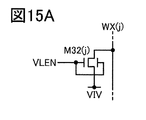
- 15A and 15B are circuit diagrams illustrating the configuration of the functional panel according to the embodiment.
- FIG. 16 is a diagram illustrating the operation of the function panel according to the embodiment.
- FIG. 17A to 17D are diagrams for explaining the configuration of the display device according to the embodiment.
- FIG. 18 is a block diagram illustrating the configuration of the input / output device according to the embodiment.
- 19A to 19C are a block diagram and a projection drawing for explaining the configuration of the information processing apparatus according to the embodiment.
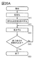
- 20A and 20B are flowcharts for explaining the driving method of the information processing apparatus according to the embodiment.
- 21A to 21C are diagrams for explaining a method of driving the information processing apparatus according to the embodiment.
- 22A to 22C are diagrams for explaining the driving method of the information processing apparatus according to the embodiment.
- 23A to 23E are diagrams for explaining the configuration of the information processing apparatus according to the embodiment.
- 24A to 24E are diagrams for explaining the configuration of the information processing apparatus according to the embodiment.
- 25A and 25B are diagrams for explaining the configuration of the information processing apparatus according to the embodiment.
- the light emitting device of one aspect of the present invention includes an insulating film, a group of structures, a layer containing a light emitting material, a first electrode, and a second electrode.
- the insulating film comprises a first surface, a group of structures comprising one structure and another structure, the other structure having a first spacing from one structure and one.
- the structure of is provided with a side wall, the side wall having an angle with the first surface, the angle being greater than 0 and less than or equal to 90 °.
- the layer containing the luminescent material comprises a first region and a second region, the first region is sandwiched between the second electrode and the first electrode, and the first region is light.
- the second region is sandwiched between the second electrode and the side wall, which reflects light.
- the first electrode includes a third region, and the third region is sandwiched between the first region and the first surface.
- a component that is guided along the layer containing the luminescent material can be efficiently extracted.
- high brightness can be obtained with less electrical energy.
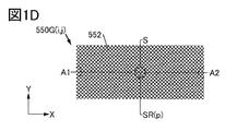
- FIG. 1 is a diagram illustrating a configuration of a light emitting device according to an aspect of the present invention.
- FIG. 1A is a perspective view of the light emitting device of one aspect of the present invention
- FIG. 1B is a top view of the light emitting device of one aspect of the present invention.
- 1C is a cross-sectional view taken along the cutting lines A1-A2 of FIG. 1B
- FIG. 1D is a top view.
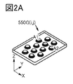
- FIG. 2 is a diagram illustrating a configuration of a light emitting device according to an aspect of the present invention.
- FIG. 2A is a perspective view of the light emitting device of one aspect of the present invention
- FIG. 2B is a top view of the light emitting device of one aspect of the present invention.
- 2C is a cross-sectional view taken along the cutting lines A1-A2 of FIG. 2B
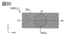
- FIG. 2D is a top view.
- FIG. 3 is a diagram illustrating a configuration of a light emitting device according to an aspect of the present invention.
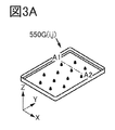
- FIG. 3A is a perspective view of the light emitting device of one aspect of the present invention
- FIG. 3B is a top view of the light emitting device of one aspect of the present invention.
- 3C is a cross-sectional view taken along the cutting lines A1-A2 of FIG. 3B
- FIG. 3D is a top view.
- FIG. 4 is a diagram illustrating a configuration of a light emitting device according to an aspect of the present invention.
- 4A is a cross-sectional view illustrating a part of the light emitting device of one aspect of the present invention shown in FIG. 1C
- FIG. 4B is a sectional view illustrating a part of the light emitting device of one aspect of the present invention shown in FIG. 2C
- FIG. 4C is a cross-sectional view illustrating a part of the light emitting device of one aspect of the present invention shown in FIG. 3C.
- a variable having an integer of 1 or more as a value may be used as a code.
- (p) containing a variable p having a value of one or more integers may be used as a part of a code for specifying any of the maximum p components.
- (m, n) including a variable m having a value of one or more integers and a variable n may be used as a part of a code for specifying any of a maximum of m ⁇ n components.
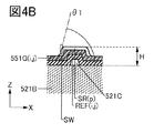
- the light emitting device 550G (i, j) described in the present embodiment includes an insulating film 521B, a structure SR (p), a layer 553G (j) containing a light emitting material, and electrodes 551G (i, j). And an electrode 552 (see FIG. 1C).
- the insulating film 521B includes a surface 521 (1).
- the structure SR (p) includes a side wall SW.
- the side wall SW has an angle ⁇ 1 with the surface 521 (1), and the angle ⁇ 1 is larger than 0 and 90 ° or less.
- a frustum-shaped shape can be used for the structure SR (p) (see FIG. 1A).
- a shape in which the angle ⁇ 1 changes continuously can be used for the structure SR (p) (see FIG. 4A).
- a shape having an S-shaped cross section can be used for the structure SR (p).
- the structure SR (p) includes a region sandwiched between the layer 553G (j) containing the luminescent material and the electrodes 551G (i, j).
- a material having a high reflectance for light PH1 can be used for the structure SR (p).
- the layer 553G (j) containing the luminescent material comprises regions 553G (j) (1) and regions 553G (j) (2) (see FIG. 1C).
- the regions 553G (j) (1) are sandwiched between the electrodes 552 and the electrodes 551G (i, j), and the regions 553G (j) (1) emit light PH1.
- the regions 553G (j) (2) are sandwiched between the electrode 552 and the side wall SW, and the side wall SW reflects light PH1.
- the electrode 551G (i, j) comprises a region 551G (i, j) (1).
- the region 551G (i, j) (1) is sandwiched between the region 553G (j) (1) and the surface 521 (1).
- the component waveguided along the layer 553G (j) containing the luminescent material can be efficiently extracted.
- high brightness can be obtained with less electrical energy.
- the light emitting device 550G (i, j) described in the present embodiment includes a reflective film REF (i, j) (see FIG. 2C).
- the reflective film REF (i, j) comprises the region REF (i, j) (1).
- the region REF (i, j) (1) sandwiches the side wall SW between the layer 553G (j) containing the luminescent material, and the region REF (i, j) (1) reflects the light PH1. ..
- a translucent conductive film can be used for the electrode 551G (i, j), and a metal film can be used for the reflective film REF (i, j).
- the thickness of the electrode 551G (i, j) can be used for adjusting the optical distance.
- the reflective film REF (i, j) can be used for the auxiliary wiring.
- a metal film may be used for the electrode 551G (i, j) to impart the function of the reflective film REF (i, j) to the electrode 551G (i, j).
- the reflective film REF (i, j) is sandwiched between the electrodes 551G (i, j) and the insulating film 521B can be used.
- the REF (i, j) comprises a region sandwiched between the region 551G (i, j) (1) and the surface 521 (1) (see FIG. 2C).
- the shape of the structure SR (p) can be controlled by using, for example, a laminated structure. Specifically, the shape of the structure SR (p) is controlled by using a structure in which the insulating film 521C formed in a frustum shape, the reflective film REF (i, j), and the electrode 551G (i, j) are laminated. Can be done (see FIG. 4B). Further, a shape in which the angle ⁇ 1 changes continuously can be used for the structure SR (p). Specifically, a shape having an S-shaped cross section can be used for the structure SR (p). As a result, it is possible to prevent a short circuit between the electrode 552 and the electrode 551G (i, j) in the vicinity of the bottom surface of the structure SR (p).
- the light emitting device 550G (i, j) described in the present embodiment includes an insulating film 521B, a structure SR (p), a layer 553G (j) containing a light emitting material, and an electrode 551G (i, j). j) and an electrode 552 (see FIG. 3C).
- the insulating film 521B includes a surface 521 (1).
- the structure SR (p) includes a side wall SW.
- the side wall SW has an angle ⁇ 1 with the surface 521 (1), and the angle ⁇ 1 is larger than 0 and 90 ° or less.
- a frustum-shaped shape can be used for the structure SR (p) (see FIG. 3A).
- a shape in which the angle ⁇ 1 changes continuously can be used for the structure SR (p) (see FIG. 4C).
- a shape having an S-shaped cross section can be used for the structure SR (p).
- the structure SR (p) includes a region sandwiched between the electrodes 551G (i, j) and the insulating film 521B.
- the layer 553G (j) containing the luminescent material comprises regions 553G (j) (1).
- the regions 553G (j) (1) are sandwiched between the electrodes 552 and the electrodes 551G (i, j), and the regions 553G (j) (1) emit light PH1.
- the electrodes 551G (i, j) include regions 551G (i, j) (1) and regions 551G (i, j) (2).
- the region 551G (i, j) (1) is sandwiched between the region 553G (j) (1) and the surface 521 (1).
- Regions 551G (i, j) (2) are sandwiched between the side wall SW and layer 553G (j) containing the luminescent material. Further, the region 551G (i, j) (2) reflects the light PH1.
- the component waveguided along the layer 553G (j) containing the luminescent material can be efficiently extracted.
- high brightness can be obtained with less electrical energy.
- the structure SR (p) has a height H from the insulating film 521B (see FIGS. 1C, 2C and 3C). Further, the structure SR (p) includes a projected area S with respect to the insulating film 521B (see FIGS. 1D, 2D, and 3D).
- the height H is 0.1 ⁇ m or more 5 ⁇ m or less, preferably 1.5 ⁇ m or 3 [mu] m or less, the projected area, 0.01 [mu] m 2 or more 100 [mu] m 2 or less, preferably 3 [mu] m 2 or more 9 .mu.m 2 or less.
- a shape in which a circle or a polygon is projected on the insulating film 521B can be used for the structure SR (p).
- the light emitting device 550G (i, j) described in the present embodiment has a group of structures (see FIGS. 1B, 2B and 3B).
- a group of structures can be arranged in a staggered pattern, for example.
- a group of structures includes structure SR (p) and other structures SR (p + 1).
- the other structure SR (p + 1) has an interval D1 between it and the structure SR (p).
- the interval D1 is 0.1 ⁇ m or more and 5 ⁇ m or less, preferably 0.1 ⁇ m or more and 2.5 ⁇ m or less.
- the distance from the outer shape of the structure SR (p) to the outer shape of another structure SR (p + 1) is defined as the interval D1.
- the components that waveguide along the layer 553G (j) containing the luminescent material can be efficiently extracted at a plurality of locations.
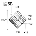
- FIG. 5 is a diagram illustrating a configuration of a functional panel according to an aspect of the present invention.
- 5A is a cross-sectional view illustrating a part of pixels 702G (i, j) of the functional panel of one aspect of the present invention
- FIG. 5B is a plan view explaining a part of the elements of the pixel
- FIG. 5C is a view. It is a top view explaining a part element of the pixel of composition different from 5B.
- 5D is a sectional view taken along line X21-X22 of FIG. 5B
- FIG. 5E is a sectional view taken along line Y21-Y22 of FIG. 5B
- FIG. 5F is a sectional view taken along line XY1-XY2 of FIG. 5C. It is a figure.
- ⁇ Configuration example 1 of function panel 700> The functional panel described in this embodiment has pixels 702G (i, j).
- Pixels 702G (i, j) include a microlens array MLA and a light emitting device 550G (i, j) (see FIG. 5A).
- the light emitting device 550G (i, j) emits light PH1.
- the light emitting device 550G (i, j) described in the first embodiment can be used.
- the microlens array MLA collects light PH1.
- the microlens array MLA includes a plurality of microlens MLs (see FIG. 5B).
- the microlens ML has a cross section having a shape that can be arranged in a plane (for example, plane XY) parallel to the light emitting device 550G (i, j) with a filling factor higher than a circle.
- the microlens ML has a curved surface in a plane (for example, plane XZ or plane YZ) orthogonal to the plane XY (see FIGS. 5D to 5F).
- the curved surface has a convex portion directed to the light emitting device 550G (i, j) (see FIG. 5A).
- a spherical surface or an aspherical surface can be used for the curved surface.
- the microlens ML has a refractive index different from that of the sealing material 705.
- a material having a refractive index higher than that of the sealing material 705 can be used for the microlens.
- the thickness of the microlens ML can be reduced without reducing the light receiving area as compared with the configuration in which one microlens is used for condensing.
- the microlens ML can be arranged close to the light emitting device 550G (i, j).
- the thickness of the functional panel can be reduced.
- a plurality of microlenses can be arranged without gaps.
- the area can be effectively used. As a result, it is possible to provide a new functional panel that is excellent in convenience, usefulness, or reliability.
- Pixels 702G (i, j) include a microlens ML and a light emitting device 550G (i, j).
- the light emitting device 550G (i, j) emits light PH1.
- microlens ML concentrates the light PH1, and the microlens ML directs the convex portion toward the light emitting device 550G (i, j).
- the microlens ML is a Frennel lens.
- the thickness of the microlens ML can be reduced without reducing the light receiving area as compared with the configuration in which one microlens is used for condensing.
- the microlens ML can be arranged close to the light emitting device 550G (i, j).
- the thickness of the functional panel can be reduced. As a result, it is possible to provide a new functional panel that is excellent in convenience, usefulness, or reliability.
- Pixels 702G (i, j) include a color conversion layer CC (G) (see FIG. 5A).
- the microlens ML is sandwiched between the light emitting device 550G (i, j) and the color conversion layer CC (G), and the microlens ML concentrates the optical PH1 on the color conversion layer CC (G).
- the color conversion layer CC (G) converts light PH1 into light PH2, and the light PH2 has a spectrum having a longer wavelength and a higher intensity of light than the spectrum of light PH1.
- a material that emits light having a wavelength longer than the wavelength of the incident light can be used for the color conversion layer CC (G).
- a material that absorbs blue light or ultraviolet light and converts it into green light and emits it a material that absorbs blue light or ultraviolet light and converts it into red light and emits it, or a material that absorbs ultraviolet light and emits blue light.
- a material that converts and emits light can be used for the color conversion layer.
- quantum dots having a diameter of several nm can be used for the color conversion layer. This makes it possible to emit light having a spectrum with a narrow half width. Alternatively, it can emit highly saturated light.
- the light PH1 emitted by the light emitting device 550G (i, j) can be focused on the color conversion layer CC (G).
- the light PH1 emitted by the light emitting device 550G (i, j) can be condensed and then converted into the light PH2.
- the light PH1 emitted by the light emitting device 550G (i, j) has higher directivity than the light emitted from the color conversion layer CC (G), it can be efficiently focused.
- the light PH1 emitted by the light emitting device 550G (i, j) can be efficiently used rather than condensing the light emitted from the color conversion layer CC (G).
- the functional panel described in this embodiment has an insulating film 528.
- Insulating film 528 has an opening, which overlaps the light emitting device 550G (i, j) (see FIG. 5A). Since the insulating film 528 has a function of separating a plurality of adjacent pixels, it can be rephrased as a partition wall.
- Configuration example of structure SR (p) A material having a high reflectance for light PH1 can be used for the structure SR (p).
- the light PH1 emitted by the light emitting device 550G (i, j) can be collected in the microlens ML.
- the optical PH1 emitted by the light emitting device 550G (i, j) can be effectively used.
- the color conversion layer CC (G) contains quantum dots and a translucent resin.
- the quantum dots can be coated with a film that is translucent and does not easily generate a gas, or a film that does not easily transmit a gas.
- a resin polymerized with quantum dots can be used.
- a photosensitive polymer that coats the quantum dots can be used.
- a fine color conversion layer CC (G) can be formed.
- the width of the spectrum of the optical PH2 can be narrowed.
- light having a narrow half width of the spectrum can be used.
- a highly saturated color can be displayed.
- the functional panel of one aspect of the present invention has a light-shielding layer BM. It also has a colored layer CF (G).
- the light-shielding layer BM has an opening, which overlaps the light emitting device 550G (i, j).
- Colored layer CF (G) has a transmittance lower than that for light PH2 with respect to light PH1.
- the amount of external light that reaches the color conversion layer CC (G) can be reduced.
- unintended conversion of external light by the color conversion layer CC (G) can be suppressed.
- the display quality can be improved. As a result, it is possible to provide a new functional panel that is excellent in convenience, usefulness, or reliability.
- FIG. 6 is a diagram illustrating a configuration of a functional panel according to an aspect of the present invention.
- FIG. 6A is a top view illustrating the configuration of a functional panel according to one aspect of the present invention
- FIG. 6B is a diagram illustrating a part of FIG. 6A.
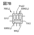
- FIG. 7A is a diagram for explaining a part of FIG. 6A
- FIG. 7B is a diagram for explaining a part of FIG. 7A
- FIG. 7C is a diagram for explaining another part of FIG. 7A.
- FIG. 8 is a diagram illustrating a configuration of a functional panel according to an aspect of the present invention.
- FIG. 8 is a circuit diagram illustrating the configuration of the pixel circuit.
- FIG. 9 is a diagram illustrating a configuration of a functional panel according to an aspect of the present invention.
- FIG. 9 is a circuit diagram illustrating the configuration of the pixel circuit.
- the functional panel 700 has a set of pixels 703 (i, j) (see FIG. 6A).
- a set of pixels 703 (i, j) includes pixels 702G (i, j) (see FIG. 6B).
- the pixel 702G (i, j) includes a pixel circuit 530G (i, j) and a light emitting device 550G (i, j), and the light emitting device 550G (i, j) is electrically connected to the pixel circuit 530G (i, j). Connected (see Figure 7A).
- the light emitting device 550G (i, j) described in the first embodiment can be used.
- the pixel circuit 530G (i, j) includes a switch SW21, a switch SW22, a transistor M21, a capacitance C21, and a node N21 (see FIG. 8).
- the transistor M21 has a gate electrode electrically connected to the node N21, a first electrode electrically connected to the light emitting device 550G (i, j), and a second electrode electrically connected to the conductive film ANO.
- the electrodes are provided.
- the switch SW21 is based on the potential of the first terminal electrically connected to the node N21, the second terminal electrically connected to the conductive film S1g (j), and the conductive film G1 (i). It has a function to control the conducting state or the non-conducting state.
- the switch SW22 has a first terminal electrically connected to the conductive film S2g (j) and a function of controlling a conductive state or a non-conductive state based on the potential of the conductive film G2 (i).
- the capacitance C21 includes a conductive film that is electrically connected to the node N21 and a conductive film that is electrically connected to the second electrode of the switch SW22.
- the image signal can be stored in the node N21.
- the potential of the node N21 can be changed by using the switch SW22.
- the intensity of the light emitted by the light emitting device 550G (i, j) can be controlled by using the potential of the node N21. As a result, it is possible to provide a new functional panel having excellent convenience or reliability.
- ⁇ Configuration Example 1 of Light Emitting Device 550G (i, j) For example, an organic electroluminescence element, an inorganic electroluminescence element, a light emitting diode, a QD LED (Quantum Dot LED), or the like can be used for the light emitting device 550G (i, j).
- an organic electroluminescence element an inorganic electroluminescence element, a light emitting diode, a QD LED (Quantum Dot LED), or the like can be used for the light emitting device 550G (i, j).
- Pixel 703 (i, j) includes pixel 702S (i, j) (see FIG. 6B).
- the pixel 702S (i, j) includes a pixel circuit 530S (i, j) and a photoelectric conversion element PD (i, j), and the photoelectric conversion element PD (i, j) includes a pixel circuit 530S (i, j) and electricity. (See FIG. 7A).
- the pixel circuit 530S (i, j) includes a switch SW31, a switch SW32, a switch SW33, a transistor M31, a capacitance C31, and a node FD (see FIG. 9A).
- the switch SW31 has a potential of a first terminal electrically connected to the photoelectric conversion element PD (i, j), a second terminal electrically connected to the node FD, and a conductive film TX (i). Based on this, it has a function of controlling a conducting state or a non-conducting state.
- the switch SW32 is in a conductive state or is based on the potential of the first terminal electrically connected to the node FD, the second terminal electrically connected to the conductive film VR, and the conductive film RS (i). It has a function to control the non-conducting state.
- the capacitance C31 includes a conductive film that is electrically connected to the node FD and a conductive film that is electrically connected to the conductive film VCP.
- the transistor M31 includes a gate electrode electrically connected to the node FD and a first electrode electrically connected to the conductive film VPI.
- the switch SW33 is of the first terminal electrically connected to the second electrode of the transistor M31, the second terminal electrically connected to the conductive film WX (j), and the conductive film SE (i). It has a function of controlling a conductive state or a non-conductive state based on a potential.
- the image pickup signal generated by the photoelectric conversion element PD (i, j) can be transferred to the node FD by using the switch SW31.
- the imaging signal generated by the photoelectric conversion element PD (i, j) can be stored in the node FD by using the switch SW31.
- the switch SW31 can be used to bring the pixel circuit 530S (i, j) and the photoelectric conversion element PD (i, j) into a non-conducting state.
- the correlated double sampling method can be applied.
- the noise included in the image pickup signal can be reduced. As a result, it is possible to provide a new functional panel having excellent convenience or reliability.
- ⁇ Configuration Example 1 of Photoelectric Conversion Element PD (i, j) For example, a heterojunction type photoelectric conversion element, a bulk heterojunction type photoelectric conversion element, or the like can be used for the photoelectric conversion element PD (i, j).
- a plurality of pixels can be used for the pixel 703 (i, j). For example, it is possible to use a plurality of pixels that display colors having different hues. It should be noted that each of the plurality of pixels can be paraphrased as a sub-pixel. Alternatively, a plurality of sub-pixels can be combined into a set and can be paraphrased as a pixel.
- the colors displayed by the plurality of pixels can be additively mixed or subtracted.
- pixels 702B (i, j) for displaying blue, pixels 702G (i, j) for displaying green, and pixels 702R (i, j) for displaying red are used for pixels 703 (i, j). be able to. Further, each of the pixels 702B (i, j), the pixels 702G (i, j) and the pixels 702R (i, j) can be paraphrased as sub-pixels (see FIG. 6B).
- a pixel displaying white or the like can be used for the pixel 703 (i, j) in addition to the above set.
- pixels for displaying cyan, pixels for displaying magenta, and pixels for displaying yellow can be used for the pixels 703 (i, j).
- a pixel that emits infrared rays can be used for the pixel 703 (i, j) in addition to the above set.
- a pixel that emits light including light having a wavelength of 650 nm or more and 1000 nm or less can be used for pixel 703 (i, j).
- FIG. 10 is a diagram illustrating a configuration of a functional panel according to an aspect of the present invention.
- FIG. 10 is a cross-sectional view taken along the cutting lines X1-X2, X3-X4, X9-X10, X11-X12 and pixels of FIG. 6A.
- FIG. 11 is a diagram illustrating a configuration of a functional panel according to an aspect of the present invention.
- 11A is a cross-sectional view of the pixel 702G (i, j) shown in FIG. 6B, and
- FIG. 11B is a cross-sectional view illustrating a part of FIG. 11A.
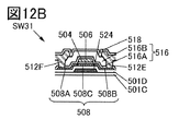
- FIG. 12 is a diagram illustrating a configuration of a functional panel according to an aspect of the present invention.
- 12A is a cross-sectional view of the pixel 702S (i, j) shown in FIG. 6B
- FIG. 12B is a cross-sectional view illustrating a part of FIG. 12A.
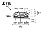
- FIG. 13 is a diagram illustrating a configuration of a functional panel according to an aspect of the present invention.
- 13A is a cross-sectional view taken along the cutting lines X1-X2 and X3-X4 of FIG. 6A
- FIG. 13B is a diagram illustrating a part of FIG. 13A.
- the functional panel of one aspect of the present invention has a functional layer 520 (see FIG. 10).
- the functional layer 520 includes a pixel circuit 530G (i, j) (see FIG. 10).
- the functional layer 520 includes, for example, the transistor M21 used in the pixel circuit 530G (i, j) (see FIGS. 8 and 11A).
- the functional layer 520 includes an opening 591G.
- the pixel circuit 530G (i, j) is electrically connected to the light emitting device 550G (i, j) at the opening 591G (see FIGS. 10 and 11). Further, the functional layer 520 includes an opening 591B.
- the functional layer 520 includes a pixel circuit 530S (i, j) (see FIG. 10).
- the functional layer 520 includes, for example, a transistor used for the switch SW31 of the pixel circuit 530S (i, j) (see FIGS. 10 and 12A).
- the transistor includes a semiconductor film 508, a conductive film 504, a conductive film 512E, and a conductive film 512F.
- the functional layer 520 includes an opening 591S, and the pixel circuit 530S (i, j) is electrically connected to the photoelectric conversion element PD (i, j) at the opening 591S (see FIGS. 10 and 12A).
- the pixel circuit 530G (i, j) can be formed on the functional layer 520.
- the pixel circuit 530S (i, j) can be formed on the functional layer 520.
- the semiconductor film used for the pixel circuit 530S (i, j) can be formed in the step of forming the semiconductor film used for the pixel circuit 530G (i, j).
- the manufacturing process of the functional panel can be simplified. As a result, it is possible to provide a new functional panel that is excellent in convenience, usefulness, or reliability.
- the functional layer 520 includes a drive circuit GD (see FIGS. 6A and 10).
- the functional layer 520 includes, for example, a transistor MD used in the drive circuit GD (see FIGS. 10 and 13A).
- the transistor MD includes a semiconductor film 508, a conductive film 504, a conductive film 512C, and a conductive film 512D.
- the functional layer 520 includes a drive circuit RD and a read circuit RC (see FIG. 10).
- the semiconductor film used for the drive circuit GD can be formed.
- the semiconductor film used for the drive circuit RD and the readout circuit RC can be formed.
- the manufacturing process of the functional panel can be simplified. As a result, it is possible to provide a new functional panel that is excellent in convenience, usefulness, or reliability.
- Transistor configuration example A bottom gate type transistor, a top gate type transistor, or the like can be used for the functional layer 520. Specifically, a transistor can be used as a switch.
- the transistor includes a semiconductor film 508, a conductive film 504, a conductive film 512A and a conductive film 512B (see FIG. 11B).
- the semiconductor film 508 includes a region 508A electrically connected to the conductive film 512A and a region 508B electrically connected to the conductive film 512B.
- the semiconductor film 508 includes a region 508C between the regions 508A and 508B.
- the conductive film 504 includes a region overlapping the region 508C, and the conductive film 504 has a function of a gate electrode.
- the insulating film 506 includes a region sandwiched between the semiconductor film 508 and the conductive film 504.
- the insulating film 506 has the function of a gate insulating film.
- the conductive film 512A has one of the functions of the source electrode and the function of the drain electrode, and the conductive film 512B has the function of the source electrode and the function of the drain electrode.
- the conductive film 524 can be used for the transistor.
- the conductive film 524 includes a region sandwiching the semiconductor film 508 with the conductive film 504.
- the conductive film 524 has the function of a second gate electrode.
- the semiconductor film used for the transistor of the pixel circuit In the step of forming the semiconductor film used for the transistor of the pixel circuit, the semiconductor film used for the transistor of the drive circuit can be formed.
- a semiconductor containing a Group 14 element can be used for the semiconductor film 508.
- a semiconductor containing silicon can be used for the semiconductor film 508.
- Hydroated amorphous silicon can be used for the semiconductor film 508.
- microcrystalline silicon or the like can be used for the semiconductor film 508. Thereby, for example, it is possible to provide a functional panel having less display unevenness than a functional panel using polysilicon for the semiconductor film 508. Alternatively, it is easy to increase the size of the functional panel.
- polysilicon can be used for the semiconductor film 508.
- the electric field effect mobility of the transistor can be made higher than that of the transistor using hydrogenated amorphous silicon for the semiconductor film 508.
- the driving ability can be enhanced as compared with a transistor using hydrogenated amorphous silicon for the semiconductor film 508.
- the aperture ratio of the pixel can be improved as compared with a transistor using hydrogenated amorphous silicon for the semiconductor film 508.
- the reliability of the transistor can be improved as compared with a transistor using hydrogenated amorphous silicon for the semiconductor film 508.
- the temperature required for manufacturing the transistor can be made lower than that of a transistor using, for example, single crystal silicon.
- the semiconductor film used for the transistor of the drive circuit can be formed by the same process as the semiconductor film used for the transistor of the pixel circuit.
- the drive circuit can be formed on the same substrate as the substrate on which the pixel circuit is formed. Alternatively, the number of parts constituting the electronic device can be reduced.
- single crystal silicon can be used for the semiconductor film 508.
- a functional panel having a higher definition than a functional panel using hydrogenated amorphous silicon for the semiconductor film 508.
- a functional panel having less display unevenness than a functional panel using polysilicon for the semiconductor film 508.
- smart glasses or head-mounted displays can be provided.
- a metal oxide can be used for the semiconductor film 508.
- the time during which the pixel circuit can hold the image signal can be lengthened as compared with the pixel circuit using a transistor using amorphous silicon as the semiconductor film.
- the selection signal can be supplied at a frequency of less than 30 Hz, preferably less than 1 Hz, more preferably less than once a minute, while suppressing the occurrence of flicker.
- the fatigue accumulated in the user of the information processing device can be reduced.
- the power consumption associated with driving can be reduced.
- the time during which the pixel circuit can hold an image pickup signal can be lengthened.
- the second selection signal can be supplied at a frequency of less than 30 Hz, preferably less than 1 Hz, more preferably less than once a minute.
- a transistor using an oxide semiconductor can be used.
- an oxide semiconductor containing indium or an oxide semiconductor containing indium, gallium, and zinc can be used for the semiconductor film.
- a transistor whose leakage current in the off state is smaller than that of a transistor using amorphous silicon for the semiconductor film can be used.
- a transistor using an oxide semiconductor as a semiconductor film can be used for a switch or the like.
- the potential of the floating node can be maintained for a longer time than in a circuit using a transistor using amorphous silicon as a switch.
- a film having a thickness of 25 nm containing indium, gallium, and zinc can be used for the semiconductor film 508.
- a conductive film in which a film having a thickness of 10 nm containing tantalum and nitrogen and a film having a thickness of 300 nm containing copper is laminated can be used for the conductive film 504.
- the copper-containing film includes a region sandwiching the tantalum and nitrogen-containing film between the copper-containing film and the insulating film 506.
- a laminated film in which a film having a thickness of 400 nm containing silicon and nitrogen and a film having a thickness of 200 nm containing silicon, oxygen and nitrogen are laminated can be used as the insulating film 506.
- the film containing silicon and nitrogen includes a region sandwiching the film containing silicon, oxygen and nitrogen between the film and the semiconductor film 508.
- a conductive film in which a film having a thickness of 50 nm containing tungsten, a film having a thickness of 400 nm containing aluminum, and a film having a thickness of 100 nm containing titanium are laminated in this order is formed on the conductive film 512A or 512B.
- the film containing tungsten includes a region in contact with the semiconductor film 508.
- a bottom gate type transistor manufacturing line using amorphous silicon for a semiconductor can be easily modified into a bottom gate type transistor manufacturing line using an oxide semiconductor for a semiconductor.
- a manufacturing line for a top gate type transistor using polysilicon as a semiconductor can be easily modified into a manufacturing line for a top gate type transistor using an oxide semiconductor for a semiconductor. Both modifications can make effective use of existing production lines.
- the flicker of the display can be suppressed.
- the power consumption can be reduced.
- a fast-moving moving image can be displayed smoothly.
- a photograph or the like can be displayed with rich gradation. As a result, it is possible to provide a new functional panel that is excellent in convenience, usefulness, or reliability.
- a compound semiconductor can be used as a semiconductor of a transistor.
- a semiconductor containing gallium arsenide can be used.
- an organic semiconductor can be used as a semiconductor of a transistor.
- an organic semiconductor containing polyacenes or graphene can be used for the semiconductor film.
- the capacitance includes one conductive film, another conductive film and an insulating film.
- the insulating film includes a region sandwiched between one conductive film and another conductive film.
- a conductive film used for the source electrode or drain electrode of the transistor, a conductive film used for the gate electrode, and an insulating film used for the gate insulating film can be used for the capacitance.
- the functional layer 520 includes an insulating film 521, an insulating film 518, an insulating film 516, an insulating film 506, an insulating film 501C, and the like (see FIGS. 11A and 11B). Further, the insulating film 521 includes an insulating film 521A and an insulating film 521B, and the insulating film 516 includes an insulating film 516A and an insulating film 516B.
- the insulating film 521 includes a region sandwiched between the pixel circuit 530G (i, j) and the light emitting device 550G (i, j).
- the insulating film 518 includes a region sandwiched between the insulating film 521 and the insulating film 501C.
- the insulating film 516 includes a region sandwiched between the insulating film 518 and the insulating film 501C.
- the insulating film 506 includes a region sandwiched between the insulating film 516 and the insulating film 501C.
- Insulating film 521 For example, an insulating inorganic material, an insulating organic material, or an insulating composite material containing the inorganic material and the organic material can be used for the insulating film 521.
- an inorganic oxide film, an inorganic nitride film, an inorganic nitride film, or a laminated material obtained by laminating a plurality of selected materials thereof can be used for the insulating film 521.
- a silicon oxide film, a silicon nitride film, a silicon nitride film, an aluminum oxide film, or a film containing a laminated material selected from these can be used as the insulating film 521.
- the silicon nitride film is a dense film and has an excellent function of suppressing the diffusion of impurities.
- polyester, polyolefin, polyamide, polyimide, polycarbonate, polysiloxane, acrylic resin, etc., or a laminated material or a composite material of a plurality of resins selected from these can be used for the insulating film 521.
- polyimide has excellent properties such as thermal stability, insulating property, toughness, low dielectric constant, low coefficient of thermal expansion, and chemical resistance as compared with other organic materials.
- polyimide can be particularly preferably used for the insulating film 521 and the like.
- the insulating film 521 may be formed by using a material having photosensitivity. Specifically, a film formed by using photosensitive polyimide, photosensitive acrylic resin, or the like can be used as the insulating film 521.
- the insulating film 521 can flatten, for example, steps derived from various structures overlapping the insulating film 521.
- Insulating film 518 For example, a material that can be used for the insulating film 521 can be used for the insulating film 518.
- a material having a function of suppressing diffusion of oxygen, hydrogen, water, alkali metal, alkaline earth metal and the like can be used for the insulating film 518.
- a nitride insulating film can be used for the insulating film 518.
- silicon nitride, silicon nitride, aluminum nitride, aluminum nitride and the like can be used for the insulating film 518. This makes it possible to suppress the diffusion of impurities into the semiconductor film of the transistor.
- Insulating film 516 For example, a material that can be used for the insulating film 521 can be used for the insulating film 516.
- a film having a manufacturing method different from that of the insulating film 518 can be used for the insulating film 516.
- Insulating film 506 For example, a material that can be used for the insulating film 521 can be used for the insulating film 506.
- a film containing a lanthanum oxide film, a cerium oxide film or a neodymium oxide film can be used for the insulating film 506.
- the insulating film 501D includes a region sandwiched between the insulating film 501C and the insulating film 516.
- a material that can be used for the insulating film 506 can be used for the insulating film 501D.
- Insulating film 501C For example, a material that can be used for the insulating film 521 can be used for the insulating film 501C. Specifically, a material containing silicon and oxygen can be used for the insulating film 501C. This makes it possible to suppress the diffusion of impurities into the pixel circuit, the light emitting element, the photoelectric conversion element, or the like.
- the functional layer 520 includes conductive films, wiring and terminals.
- a conductive material can be used for wiring, electrodes, terminals, conductive films and the like.
- an inorganic conductive material for example, an inorganic conductive material, an organic conductive material, a metal, a conductive ceramic, or the like can be used for wiring or the like.
- metal elements selected from aluminum, gold, platinum, silver, copper, chromium, tantalum, titanium, molybdenum, tungsten, nickel, iron, cobalt, palladium or manganese can be used for wiring and the like. ..
- the above-mentioned alloy containing a metal element or the like can be used for wiring or the like.
- an alloy of copper and manganese is suitable for microfabrication using a wet etching method.
- a two-layer structure in which a titanium film is laminated on an aluminum film a two-layer structure in which a titanium film is laminated on a titanium nitride film, a two-layer structure in which a tungsten film is laminated on a titanium nitride film, a tantalum nitride film or
- a two-layer structure in which a tungsten film is laminated on a tungsten nitride film, a titanium film, and a three-layer structure in which an aluminum film is laminated on the titanium film and a titanium film is further formed on the titanium film can be used for wiring or the like. ..
- conductive oxides such as indium oxide, indium tin oxide, indium zinc oxide, zinc oxide, and zinc oxide added with gallium can be used for wiring and the like.
- a film containing graphene or graphite can be used for wiring or the like.
- a graphene-containing film can be formed by forming a film containing graphene oxide and reducing the film containing graphene oxide.
- Examples of the method of reduction include a method of applying heat and a method of using a reducing agent.
- a film containing metal nanowires can be used for wiring and the like.
- nanowires containing silver can be used.
- a conductive polymer can be used for wiring and the like.
- the terminal 519B can be electrically connected to the flexible printed circuit board FPC1 by using a conductive material (see FIG. 10).
- the conductive material CP can be used to electrically connect the terminal 519B to the flexible printed circuit board FPC1.
- the functional panel 700 includes a base material 510, a base material 770, and a sealing material 705 (see FIG. 11A). Further, the functional panel 700 includes a structure KB.
- Base material 510, base material 770 >> A translucent material can be used for the substrate 510 or the substrate 770.
- a flexible material can be used for the substrate 510 or the substrate 770. Thereby, it is possible to provide a functional panel having flexibility.
- a material having a thickness of 0.7 mm or less and a thickness of 0.1 mm or more can be used.
- a material polished to a thickness of about 0.1 mm can be used. Thereby, the weight can be reduced.
- glass substrates of the 6th generation (1500 mm ⁇ 1850 mm), the 7th generation (1870 mm ⁇ 2200 mm), the 8th generation (2200 mm ⁇ 2400 mm), the 9th generation (2400 mm ⁇ 2800 mm), the 10th generation (2950 mm ⁇ 3400 mm), etc. can be used for the base material 510 or the base material 770. As a result, a large display device can be manufactured.
- An organic material, an inorganic material, or a composite material such as an organic material and an inorganic material can be used for the base material 510 or the base material 770.
- inorganic materials such as glass, ceramics, and metal can be used.
- non-alkali glass, soda-lime glass, potash glass, crystal glass, aluminosilicate glass, tempered glass, chemically tempered glass, quartz, sapphire and the like can be used for the base material 510 or the base material 770.
- aluminosilicate glass, tempered glass, chemically tempered glass, sapphire, or the like can be suitably used for the base material 510 or the base material 770 arranged closer to the user of the functional panel. As a result, it is possible to prevent the functional panel from being damaged or scratched due to use.
- an inorganic oxide film, an inorganic nitride film, an inorganic oxynitride film, or the like can be used.
- a silicon oxide film, a silicon nitride film, a silicon nitride film, an aluminum oxide film, or the like can be used.
- Stainless steel, aluminum and the like can be used for the base material 510 or the base material 770.
- a single crystal semiconductor substrate made of silicon or silicon carbide, a polycrystalline semiconductor substrate, a compound semiconductor substrate such as silicon germanium, an SOI substrate, or the like can be used as the base material 510 or the base material 770.
- the semiconductor element can be formed on the base material 510 or the base material 770.
- an organic material such as resin, resin film or plastic can be used for the base material 510 or the base material 770.
- a material containing a resin having a siloxane bond such as polyester, polyolefin, polyamide (nylon, aramid, etc.), polyimide, polycarbonate, polyurethane or acrylic resin, epoxy resin or silicone is used as the base material 510 or the base material 770.
- a resin film, a resin plate, a laminated material, or the like containing these materials can be used. Thereby, the weight can be reduced. Alternatively, for example, the frequency of occurrence of damage due to dropping can be reduced.
- PET polyethylene terephthalate
- PEN polyethylene naphthalate
- PES polyether sulfone
- COP cycloolefin polymer
- COC cycloolefin copolymer
- a composite material obtained by laminating a film such as a metal plate, a thin glass plate, or an inorganic material and a resin film or the like can be used for the base material 510 or the base material 770.
- a composite material in which a fibrous or particulate metal, glass, or an inorganic material is dispersed in a resin can be used for the base material 510 or the base material 770.
- a composite material in which a fibrous or particulate resin or an organic material is dispersed in an inorganic material can be used for the base material 510 or the base material 770.
- a single-layer material or a material in which a plurality of layers are laminated can be used for the base material 510 or the base material 770.
- a material in which an insulating film or the like is laminated can be used.
- a material in which one or more films selected from a silicon oxide layer, a silicon nitride layer, a silicon nitride layer, and the like are laminated can be used. This makes it possible to prevent the diffusion of impurities contained in the base material, for example. Alternatively, it is possible to prevent the diffusion of impurities contained in the glass or resin. Alternatively, it is possible to prevent the diffusion of impurities that permeate the resin.
- paper, wood or the like can be used for the base material 510 or the base material 770.
- a material having heat resistance sufficient to withstand the heat treatment during the manufacturing process can be used for the base material 510 or the base material 770.
- a material having heat resistance to heat applied during the manufacturing process of directly forming a transistor, a capacitance, or the like can be used for the base material 510 or the base material 770.
- an insulating film, a transistor, a capacitance, or the like is formed on a process substrate having heat resistance to heat applied during the manufacturing process, and the formed insulating film, the transistor, the capacitance, or the like is applied to, for example, the substrate 510 or the substrate 770.
- a transposition method can be used. Thereby, for example, an insulating film, a transistor, a capacitance, or the like can be formed on a flexible substrate.
- the sealing material 705 includes a region sandwiched between the functional layer 520 and the base material 770, and has a function of bonding the functional layer 520 and the base material 770 (see FIG. 11A).
- An inorganic material, an organic material, a composite material of an inorganic material and an organic material, or the like can be used for the sealing material 705.
- an organic material such as a heat-meltable resin or a curable resin can be used for the sealing material 705.
- organic materials such as reaction curable adhesives, photocurable adhesives, thermosetting adhesives and / and anaerobic adhesives can be used for the encapsulant 705.
- PVC polyvinyl chloride
- PVB polyvinyl chloride
- EVA ethylene vinyl acetate
- the structure KB comprises a region sandwiched between the functional layer 520 and the substrate 770. Further, the structure KB has a function of providing a predetermined gap between the functional layer 520 and the base material 770.
- the functional panel 700 includes a light emitting device 550G (i, j) (see FIG. 11).
- the light emitting device 550G (i, j) described in the first embodiment can be used.
- a layer 553G (j) containing an electrode 551G (i, j), an electrode 552 and a luminescent material can be used in the light emitting device 550G (i, j). Further, the layer 553G (j) containing the luminescent material includes a region sandwiched between the electrodes 551G (i, j) and the electrodes 552.
- the laminated material can be used for layer 553G (j) containing a luminescent material.
- a material that emits blue light, a material that emits green light, a material that emits red light, a material that emits infrared rays, or a material that emits ultraviolet rays can be used for the layer 553G (j) containing a luminescent material. ..
- a plurality of materials that emit light having different hues can be used for the layer 553G (j) containing the luminescent material.
- a laminated material obtained by laminating a layer containing a luminescent material containing a fluorescent material that emits blue light and a layer containing a material other than the fluorescent material that emits green and red light includes the luminescent material. It can be used for layer 553G (j).
- a laminated material obtained by laminating a layer containing a luminescent material containing a fluorescent material that emits blue light and a layer containing a material other than the fluorescent material that emits yellow light includes the luminescent material. It can be used for layer 553G (j).
- the colored layer CF can be used by superimposing the colored layer CF on the layer 553G (j) containing the luminescent material. As a result, light having a predetermined hue can be extracted from the white light.
- a laminated material laminated to emit blue light or ultraviolet light can be used for layer 553G (j) containing a luminescent material.
- the color conversion layers CC can be stacked and used.
- the layer 553G (j) containing the luminescent material comprises a luminescent unit.
- the light emitting unit includes one region in which an electron injected from one side recombines with a hole injected from the other side. Further, the light emitting unit includes a light emitting material, and the light emitting material emits energy generated by recombination of electrons and holes as light.
- the hole transport layer and the electron transport layer can be used for the light emitting unit.
- the hole transport layer is arranged on the positive electrode side of the electron transport layer, and the hole transport layer has higher hole mobility than the electron transport layer.
- a plurality of light emitting units and an intermediate layer can be used for the layer 553G (j) containing a light emitting material.
- the intermediate layer comprises a region sandwiched between the two light emitting units.
- the intermediate layer has a charge generation region, and the intermediate layer has a function of supplying holes to a light emitting unit arranged on the cathode side and supplying electrons to a light emitting unit arranged on the anode side.
- a configuration including a plurality of light emitting units and an intermediate layer may be referred to as a tandem type light emitting element.
- the current efficiency related to light emission can be increased.
- the current density flowing through the light emitting element can be reduced at the same brightness.
- the reliability of the light emitting element can be improved.
- a light emitting unit containing a material that emits light of one hue can be superposed on a light emitting unit that contains a material that emits light of another hue, and can be used for the layer 553G (j) containing the light emitting material.
- a light emitting unit containing a material that emits light of one hue can be superposed on a light emitting unit that contains a material that emits light of the same hue, and can be used for the layer 553G (j) containing the light emitting material.
- two light emitting units containing a material that emits blue light can be used in an overlapping manner.
- a polymer compound oligomer, dendrimer, polymer, etc.
- a medium molecular compound a compound in the intermediate region between a small molecule and a polymer: a compound having a molecular weight of 400 or more and 4000 or less
- a polymer compound oligomer, dendrimer, polymer, etc.
- a medium molecular compound a compound in the intermediate region between a small molecule and a polymer: a compound having a molecular weight of 400 or more and 4000 or less
- Electrode 551G (i, j), electrode 552 For example, a material that can be used for wiring or the like can be used for the electrode 551G (i, j) or the electrode 552. Specifically, a material having translucency with respect to visible light can be used for the electrode 551G (i, j) or the electrode 552.
- a conductive oxide or a conductive oxide containing indium, indium oxide, indium tin oxide, indium zinc oxide, zinc oxide, zinc oxide added with gallium, or the like can be used.
- a metal film thin enough to transmit light can be used.
- a material having translucency for visible light can be used.
- a metal film that transmits a part of light and reflects another part of light can be used for the electrode 551G (i, j) or the electrode 552.
- a layer 553G (j) containing a luminescent material is used to adjust the distance between the electrodes 551G (i, j) and the electrodes 552.
- the microcavity structure can be provided in the light emitting device 550G (i, j).
- light having a predetermined wavelength can be extracted more efficiently than other light.
- light with a narrow half width of the spectrum can be extracted.
- brightly colored light can be extracted.
- a film that efficiently reflects light can be used for the electrode 551G (i, j) or the electrode 552.
- a material containing silver, palladium, or the like or a material containing silver, copper, or the like can be used for the metal film.
- the electrode 551G (i, j) is electrically connected to the pixel circuit 530G (i, j) at the opening 591G (see FIG. 12A).
- the electrode 551G (i, j) overlaps with, for example, an opening formed in the insulating film 528, and the electrode 551G (i, j) has an insulating film 528 on the peripheral edge thereof.
- the photoelectric conversion element PD (i, j) includes an electrode 551S (i, j), an electrode 552, and a layer 553S (j) containing a photoelectric conversion material (see FIG. 12A).
- a heterojunction type photoelectric conversion element for example, a heterojunction type photoelectric conversion element, a bulk heterojunction type photoelectric conversion element, or the like can be used for the photoelectric conversion element PD (i, j).
- a laminated film in which a p-type semiconductor film and an n-type semiconductor film are laminated so as to be in contact with each other can be used for the layer 553S (j) containing a photoelectric conversion material.
- the photoelectric conversion element PD (i, j) that uses a laminated film having such a structure on the layer 553S (j) containing the photoelectric conversion material can be called a PN-type photodiode.
- the photoelectric conversion element PD (i, j) that uses a laminated film having such a structure on the layer 553S (j) containing the photoelectric conversion material can be referred to as a PIN type photodiode.
- a p-type semiconductor film is sandwiched between a p + type semiconductor film and an n-type semiconductor film, and a p-type semiconductor film is sandwiched between the p-type semiconductor film and the n-type semiconductor film.
- a laminated film obtained by laminating a p + type semiconductor film, a p-type semiconductor film, a p-type semiconductor film, and an n-type semiconductor film can be used for the layer 553S (j) containing a photoelectric conversion material.
- a photoelectric conversion element PD (i, j) that uses a laminated film having such a structure on a layer 553S (j) containing a photoelectric conversion material can be called an avalanche photodiode.
- a semiconductor containing a Group 14 element can be used for layer 553S (j) containing a photoelectric conversion material.
- a semiconductor containing silicon can be used for the layer 553S (j) containing a photoelectric conversion material.
- hydrogenated amorphous silicon, microcrystalline silicon, polysilicon, single crystal silicon, or the like can be used for layer 553S (j) containing a photoelectric conversion material.
- an organic semiconductor can be used for layer 553S (j) containing a photoelectric conversion material.
- a part of the layer used for the layer 553G (j) containing a luminescent material can be used as a part of the layer 553S (j) containing a photoelectric conversion material.
- the hole transport layer used for the layer 553G (j) containing the luminescent material can be used for the layer 553S (j) containing the photoelectric conversion material.
- the electron transport layer used for the layer 553G (j) containing the luminescent material can be used for the layer 553S (j) containing the photoelectric conversion material.
- the hole transport layer and the electron transport layer can be used for the layer 553S (j) containing the photoelectric conversion material.
- the electron transport layer used for the layer 553G (j) containing the luminescent material can be formed.
- the manufacturing process can be simplified.
- an electron-accepting organic semiconductor material such as fullerene (for example, C 60 , C 70, etc.) or a derivative thereof can be used for the n-type semiconductor film.
- an electron-donating organic semiconductor material such as copper (II) phthalocyanine (CuPc) or tetraphenyldibenzoperichanene (DBP) can be used for the p-type semiconductor film. ..
- a film in which an electron-accepting semiconductor material and an electron-donating semiconductor material are co-deposited can be used as an i-type semiconductor film.
- the functional panel 700 has an insulating film 528 and an insulating film 573 (see FIG. 11A).
- Insulating film 528 has a region sandwiched between the functional layer 520 and the base material 770, and the insulating film 528 has an opening in a region overlapping the light emitting device 550G (i, j) (see FIG. 11A).
- a material that can be used for the insulating film 521 can be used for the insulating film 528.
- a silicon oxide film, a film containing an acrylic resin, a film containing polyimide, or the like can be used for the insulating film 528.
- the insulating film 573 includes a region sandwiching the light emitting device 550G (i, j) with the functional layer 520 (see FIG. 11A).
- the insulating film 573 is formed by laminating an insulating film 573A that can form the light emitting device 550G (i, j) in a manner that is not easily damaged and a dense insulating film 573B that has few defects. It can be used.
- the diffusion of impurities into the light emitting device 550G (i, j) can be suppressed.
- the reliability of the light emitting device 550G (i, j) can be improved.
- the functional panel 700 includes a functional layer 720 (see FIG. 11A).
- the functional layer 720 includes a light-shielding layer BM, a colored layer CF (G), and an insulating film 771. Moreover, the color conversion layer CC (G) can be used.
- the light-shielding layer BM is provided with an opening in a region overlapping the pixels 702G (i, j). Further, the light-shielding layer BM is provided with an opening in a region overlapping the pixels 702S (i, j).
- a dark material can be used for the light shielding layer BM. Thereby, the contrast of the display can be improved.
- the colored layer CF (G) includes a region sandwiched between the base material 770 and the light emitting device 550G (i, j).
- a material that selectively transmits light of a predetermined color can be used for the colored layer CF (G).
- a material that transmits red light, green light, or blue light can be used for the colored layer CF (G).
- the insulating film 771 includes a region sandwiched between the base material 770 and the light emitting device 550G (i, j).
- the insulating film 771 includes a region sandwiching the light-shielding layer BM and the colored layer CF (G) between the insulating film 771 and the base material 770. As a result, the unevenness derived from the thickness of the light-shielding layer BM and the colored layer CF (G) can be flattened.
- the functional panel 700 includes a light-shielding film KBM (see FIG. 13A).
- the light-shielding film KBM is provided with an opening in a region overlapping the pixels 702S (i, j). Further, the light-shielding film KBM has a region sandwiched between the functional layer 520 and the base material 770, and has a function of providing a predetermined gap between the functional layer 520 and the base material 770. For example, a dark material can be used for the light-shielding film KBM. As a result, it is possible to suppress stray light entering the pixels 702S (i, j).
- the functional panel 700 includes a functional film 770P and the like (see FIG. 11A).
- the functional film 770P includes a region that overlaps with the light emitting device 550G (i, j).
- an antireflection film, a polarizing film, a retardation film, a light diffusing film, a condensing film and the like can be used for the functional film 770P.
- an antireflection film having a thickness of 1 ⁇ m or less can be used for the functional film 770P.
- a laminated film in which three or more layers, preferably five or more layers, and more preferably 15 or more layers of dielectrics are laminated can be used for the functional film 770P.
- the reflectance can be suppressed to 0.5% or less, preferably 0.08% or less.
- a circularly polarizing film can be used for the functional film 770P.
- an antistatic film that suppresses the adhesion of dust a water-repellent film that makes it difficult for dirt to adhere, an oil-repellent film that makes it difficult for dirt to adhere, a non-glossy film (anti-glare film), and scratches caused by use.
- a hard coat film that suppresses the generation, a self-healing film that repairs the generated scratches, and the like can be used for the functional film 770P.
- FIG. 14 is a diagram illustrating a configuration of a functional panel according to an aspect of the present invention.
- FIG. 15 is a circuit diagram illustrating a configuration of a functional panel according to an aspect of the present invention.
- FIG. 15A is a circuit diagram illustrating a part of an amplifier circuit that can be used for the functional panel of one aspect of the present invention
- FIG. 15B is a sampling circuit that can be used for the functional panel of one aspect of the present invention. It is a circuit diagram explaining a part.
- FIG. 16 is a diagram illustrating the operation of the functional panel of one aspect of the present invention.
- the functional panel 700 described in this embodiment has a region 231 (see FIG. 14).
- Region 231 includes a group of pixels 703 (i, 1) to 703 (i, n) and another group of pixels 703 (1, j) to 703 (m, j). Further, the region 231 includes a conductive film G1 (i), a conductive film TX (i), a conductive film S1g (j), and a conductive film WX (j).
- the group of pixels 703 (i, 1) to 703 (i, n) are arranged in the row direction (the direction indicated by the arrow R1 in the drawing), and the group of pixels 703 (i, 1) to 703 (i). , N) include pixels 703 (i, j).
- the group of pixels 703 (i, 1) to 703 (i, n) are electrically connected to the conductive film G1 (i), and the group of pixels 703 (i, 1) to 703 (i, n) is electrically connected.
- n) is electrically connected to the conductive film TX (i).
- the other group of pixels 703 (1, j) to 703 (m, j) are arranged in the column direction (direction indicated by the arrow C1 in the figure) intersecting the row direction, and the other group of pixels 703 ( 1, j) to pixel 703 (m, j) includes pixel 703 (i, j).
- the other group of pixels 703 (1, j) to 703 (m, j) are electrically connected to the conductive film S1g (j), and the other group of pixels 703 (1, j) to pixel 703 are electrically connected to each other.
- (M, j) is electrically connected to the conductive film WX (j).
- imaging information can be acquired from a plurality of pixels.
- image information can be supplied to a plurality of pixels.
- the region 231 has a conductive film VCOM2 and a conductive film ANO.
- the functional panel described in this embodiment has a drive circuit GD (see FIG. 14).
- the pixel circuit 530G (i, j) is supplied with the first selection signal, and the pixel circuit 530G (i, j) acquires an image signal based on the first selection signal.
- the conductive film G1 (i) can be used to supply the first selection signal (see FIG. 7B).
- the image signal can be supplied using the conductive film S1g (j).
- the operation of supplying the first selection signal and causing the pixel circuit 530G (i, j) to acquire the image signal can be referred to as “writing” (see FIG. 16).
- the light emitting device 550G (i, j) emits light based on the image signal (see FIG. 7B).
- the light emitting device 550G (i, j) includes an electrode 551G (i, j) that is electrically connected to the pixel circuit 530G (i, j) and an electrode 552 that is electrically connected to the conductive film VCOM2. (See FIGS. 8 and 11A).
- the functional panel of one aspect of the present invention has a readout circuit RC (j), a conductive film VLEN, a conductive film VIV, and a conductive film CL (see FIGS. 14, 9, 15A, and 15B).
- the functional panel also includes a conductive film CAPSEL, a conductive film CDS VDD, a conductive film CDSVSS, and a conductive film VCL.
- the read-out circuit RC (j) includes an amplifier circuit and a sampling circuit SC (j) (see FIG. 14).
- the amplifier circuit includes a transistor M32 (j) (see FIG. 15A).
- the transistor M32 (j) is electrically connected to the gate electrode electrically connected to the conductive film VLEN, the first electrode electrically connected to the conductive film WX (j), and the conductive film VIV. Provided with a second electrode.
- the conductive film WX (j) connects the transistor M31 (j) and the transistor M32 (j) (see FIGS. 9 and 15A).
- the source follower circuit can be configured by using the transistor M31 (j) and the transistor M32 (j).
- the potential of the conductive film WX (j) can be changed based on the potential of the node FD.
- the sampling circuit SC (j) includes a first terminal IN (j), a second terminal, and a third terminal OUT (j) (see FIG. 15B).
- the first terminal is electrically connected to the conductive film WX (j), the second terminal is electrically connected to the conductive film CL, and the third terminal OUT (j) is the first terminal IN (j). It has a function of supplying a signal that changes based on the potential of.
- the image pickup signal can be acquired from the pixel circuit 530S (i, j).
- a correlated double sampling method can be applied.
- a sampling circuit SC (j) can be provided for each conductive film WX (j).
- the difference signal of the pixel circuit 530S (i, j) can be acquired for each conductive film WX (j).
- the operating frequency of the sampling circuit SC (j) can be suppressed.
- noise can be reduced. As a result, it is possible to provide a new functional panel having excellent convenience or reliability.
- the functional panel 700 has a drive circuit RD (see FIG. 14).
- the drive circuit RD supplies a second selection signal and a third selection signal.
- ⁇ Configuration Example 1 of Pixel Circuit 530S (i, j) The pixel circuit 530S (i, j) is supplied with the second selection signal and the third selection signal during the period when the first selection signal is not supplied (see FIG. 16). Further, the pixel circuit 530S (i, j) acquires an image pickup signal based on the second selection signal, and supplies the image pickup signal based on the third selection signal.
- the conductive film TX (i) can be used to supply the second selection signal
- the conductive film SE (i) can be used to supply the third selection signal (see FIG. 9).
- the operation of supplying the second selection signal and causing the pixel circuit 530S (i, j) to acquire the imaging signal can be referred to as “imaging” (see FIG. 16). Further, the operation of reading the image pickup signal from the pixel circuit 530S (i, j) can be referred to as “reading”. Further, the operation of supplying a predetermined voltage to the photoelectric conversion element PD (i, j) is "initialization”, and the operation of exposing the initialized photoelectric conversion element PD (i, j) to light for a predetermined period is “initialization”. "Exposure” and the operation of reflecting the voltage changed with exposure in the pixel circuit 530S (i, j) can be referred to as "transfer”. Further, SRS in the figure corresponds to an operation of supplying a reference signal used in the correlated double sampling method, and “output” corresponds to an operation of supplying an imaging signal.
- one frame of image information can be written in 16.7 msec. Specifically, it can operate at a frame rate of 60 Hz.
- the image signal can be written to the pixel circuit 530G (i, j) in 15.2 ⁇ sec.
- one frame of image information can be retained for a period corresponding to 16 frames.
- the imaging information of one frame can be photographed and read out in a period corresponding to 16 frames.
- it can be initialized at 15 ⁇ sec, exposed at 1 msec or more and 5 msec or less, and transferred at 150 ⁇ sec. Alternatively, it can be read in 250 msec.
- the photoelectric conversion element PD (i, j) has an electrode 551S (i, j) electrically connected to the pixel circuit 530S (i, j) and an electrode 552 electrically connected to the conductive film VPD. (See FIGS. 9 and 12A). Further, the electrode 552 used for the light emitting device 550G (i, j) can be used for the photoelectric conversion element PD (i, j). This makes it possible to simplify the configuration and manufacturing process of the functional panel.
- Pixels 703 (i, j) are supplied with a second selection signal during the period in which one image signal is held.
- the pixel 703 (i, j) uses the light emitting device 550G (i, j) and is based on the image signal. , Can emit light (see FIG. 16).
- the pixel circuit 530G (i, j) acquires one image signal based on the first selection signal, before the first selection signal is supplied again, the pixel circuit 530S ( i, j) are supplied with a second selection signal.
- the intensity of the light emitted by the light emitting device 550G (i, j) can be controlled by using the image signal.
- the subject can be irradiated with light having a controlled intensity.
- the subject can be imaged by using the photoelectric conversion element PD (i, j).
- the subject can be imaged by using the photoelectric conversion element PD (i, j) while controlling the intensity of the emitted light.
- the functional panel 700 of one aspect of the present invention includes a multiplexer MUX, an amplifier circuit AMP, and an analog-to-digital conversion circuit ADC (see FIG. 14).
- the multiplexer MUX has a function of selecting one from a plurality of sampling circuits SC (j) to acquire an imaging signal and supplying it to, for example, an amplifier circuit AMP.
- the multiplexer MUX is electrically connected to the third terminal OUT (j) of the sampling circuit SC (see FIG. 15B).
- the multiplexer MUX is electrically connected to the sampling circuit SC (1) to the sampling circuit SC (9), can acquire an imaging signal from a predetermined sampling circuit, and can supply the imaging signal to the amplifier circuit AMP.
- the amplifier circuit AMP can amplify the image pickup signal and supply it to the analog-to-digital conversion circuit ADC.
- the functional layer 520 includes a multiplexer MUX and an amplifier circuit AMP.
- the semiconductor film used for the pixel circuit 530G (i, j)
- the semiconductor film used for the multiplexer MUX and the amplifier circuit AMP can be formed.
- the manufacturing process of the functional panel can be simplified. As a result, it is possible to provide a new functional panel that is excellent in convenience, usefulness, or reliability.
- the analog-to-digital conversion circuit ADC has a function of converting an analog image pickup signal into a digital signal. As a result, deterioration of the imaging signal due to transmission can be suppressed.
- FIG. 17 is a diagram illustrating a configuration of a display device according to an aspect of the present invention.
- 17A is a block diagram of the display device of one aspect of the present invention
- FIGS. 17B to 17D are projection views illustrating the appearance of the display device of one aspect of the present invention.
- the display device described in this embodiment includes a function panel 700 and a control unit 238 (see FIG. 17A). In addition, the display device has a control unit 243.
- the control unit 238 is supplied with the image information VI and the control information CI.
- a clock signal, a timing signal, or the like can be used for the control information CI.
- the control unit 238 generates information V11 based on the image information VI, and generates a control signal based on the control information CI. Further, the control unit 238 supplies the information V11 and the control signal.
- the information V11 includes a gradation of 8 bits or more, preferably 12 bits or more.
- a clock signal or a start pulse of a shift register used in a drive circuit can be used as a control signal.
- the decompression circuit 234 has a function of decompressing the image information VI supplied in a compressed state.
- the extension circuit 234 includes a storage unit.
- the storage unit has, for example, a function of storing the stretched image information.
- the image processing circuit 235 includes, for example, a storage area.
- the storage area has, for example, a function of storing information included in the image information VI.
- the image processing circuit 235 has, for example, a function of correcting the image information VI based on a predetermined characteristic curve to generate the information V11 and a function of supplying the information V11.
- the function panel 700 is supplied with information V11 and control signals.
- the functional panel 700 described in any one of the second to sixth embodiments can be used.
- an information device terminal see FIG. 17B
- a video display system see FIG. 17C
- a computer see FIG. 17D
- the like can be provided.
- the functional panel 700 includes a drive circuit and a control circuit (see FIG. 17A).
- the drive circuit operates based on the control signal. By using the control signal, the operations of a plurality of drive circuits can be synchronized.
- the drive circuit GD can be used for the functional panel 700.
- the drive circuit GD has a function of supplying a control signal and supplying a first selection signal.
- the drive circuit SD can be used for the function panel 700.
- the drive circuit SD is supplied with a control signal and information V11, and can supply an image signal.
- the drive circuit RD can be used for the function panel 700.
- the drive circuit RD is supplied with a control signal and can supply a second selection signal.
- the read circuit RC can be used for the function panel 700.
- the read-out circuit RC is supplied with a control signal, and for example, an image pickup signal can be read out by using a correlated double sampling method.
- the control circuit has a function of generating and supplying a control signal.
- a clock signal, a timing signal, or the like can be used as a control signal.
- control circuit formed on the rigid substrate can be used for the functional panel.
- flexible printed circuit board can be used to electrically connect the control circuit and the control unit 238 formed on the rigid substrate.
- Control circuit 233 For example, a timing controller can be used in the control circuit 233.
- FIG. 18 is a block diagram illustrating a configuration of an input / output device according to an aspect of the present invention.
- the input / output device described in this embodiment includes an input unit 240 and a display unit 230 (see FIG. 18).
- the display unit 230 includes a display panel.
- the functional panel 700 described in any one of the second to sixth embodiments can be used for the display unit 230.
- the configuration having the input unit 240 and the display unit 230 can be referred to as an input / output panel 700TP.
- the input unit 240 includes a detection area 241.
- the input unit 240 has a function of detecting an object close to the detection area 241.
- the detection area 241 includes an area that overlaps with the pixel 703 (i, j).
- the position information can be input by using a finger or the like close to the display unit as the pointer.
- the position information can be associated with the image information displayed on the display unit. As a result, it is possible to provide a new input / output device having excellent convenience or reliability.
- the detection area 241 includes, for example, one or more detectors.
- the detection area 241 includes a group of detectors 802 (g, 1) to 802 (g, q) and another group of detectors 802 (1, h) to 802 (p, h).
- g is an integer of 1 or more and p or less
- h is an integer of 1 or more and q or less
- p and q are integers of 1 or more.
- the group of detectors 802 (g, 1) to 802 (g, q) includes the detectors 802 (g, h) and are arranged in the row direction (direction indicated by arrow R2 in the drawing).
- the direction indicated by the arrow R2 may be the same as or different from the direction indicated by the arrow R1.
- Another group of detectors 802 (1, h) to 802 (p, h) includes the detector 802 (g, h), and the column direction intersecting the row direction (arrow C2 in the figure). It is arranged in the direction shown).
- the detector has a function of detecting a nearby pointer.
- a finger, a stylus pen, or the like can be used as a pointer.
- a metal piece, a coil, or the like can be used for the stylus pen.
- a capacitance type proximity sensor an electromagnetic induction type proximity sensor, an optical type proximity sensor, a resistance film type proximity sensor, and the like can be used as the detector.
- a plurality of types of detectors can be used together.
- a detector that detects a finger and a detector that detects a stylus pen can be used together.
- the detection information can be associated with the gesture.
- the detection information can be associated with the drawing process.
- a finger can be detected by using a capacitance type, pressure sensitive type or optical type proximity sensor.
- the stylus pen can be detected by using an electromagnetic induction type or an optical type proximity sensor.
- the input unit 240 includes an oscillation circuit OSC and a detection circuit DC (see FIG. 18).
- the oscillation circuit OSC supplies the search signal to the detector 802 (g, h).
- a square wave, a sawtooth wave, a triangular wave, a sine wave, or the like can be used as a search signal.
- the detector 802 (g, h) generates and supplies a detection signal that changes based on the distance to the pointer close to the detector 802 (g, h) and the search signal.
- the detection circuit DC supplies input information based on the detection signal.
- the distance from the adjacent pointer to the detection area 241 can be detected.
- the position where the pointer is closest to the detection area 241 can be detected.
- FIG. 19A is a block diagram illustrating a configuration of an information processing device according to an aspect of the present invention.
- 19B and 19C are projection views illustrating an example of the appearance of the information processing apparatus.
- FIG. 20 is a flowchart illustrating a program of one aspect of the present invention.
- FIG. 20A is a flowchart illustrating the main processing of the program of one aspect of the present invention
- FIG. 20B is a flowchart illustrating interrupt processing.
- FIG. 21 is a diagram illustrating a program of one aspect of the present invention.
- FIG. 21A is a flowchart illustrating interrupt processing of the program of one aspect of the present invention.
- 21B is a schematic diagram for explaining the operation of the information processing device, and
- FIG. 21C is a timing chart for explaining the operation of the information processing device according to one aspect of the present invention.
- the information processing device described in this embodiment includes an arithmetic unit 210 and an input / output device 220 (see FIG. 19A).
- the input / output device 220 is electrically connected to the arithmetic unit 210.
- the information processing device 200 can include a housing (see FIGS. 19B and 19C).
- the arithmetic unit 210 is supplied with the input information II or the detection information DS.
- the arithmetic unit 210 generates the control information CI and the image information VI based on the input information II or the detection information DS, and supplies the control information CI and the image information VI.
- the arithmetic unit 210 includes an arithmetic unit 211 and a storage unit 212. Further, the arithmetic unit 210 includes a transmission line 214 and an input / output interface 215.
- the transmission line 214 is electrically connected to the arithmetic unit 211, the storage unit 212, and the input / output interface 215.
- the calculation unit 211 has, for example, a function of executing a program.
- the storage unit 212 has a function of storing, for example, a program, initial information, setting information, an image, or the like executed by the calculation unit 211.
- a hard disk, a flash memory, a memory using a transistor including an oxide semiconductor, or the like can be used.
- the input / output interface 215 includes terminals or wiring, and has a function of supplying information and being supplied with information. For example, it can be electrically connected to the transmission line 214. Further, it can be electrically connected to the input / output device 220.
- the transmission line 214 includes wiring, supplies information, and has a function of being supplied with information. For example, it can be electrically connected to the input / output interface 215. Further, it can be electrically connected to the calculation unit 211, the storage unit 212, or the input / output interface 215.
- the input / output device 220 supplies the input information II and the detection information DS.
- the input / output device 220 is supplied with the control information CI and the image information VI (see FIG. 19A).
- keyboard scan code, position information, button operation information, voice information, image information, and the like can be used as input information II.
- illuminance information, attitude information, acceleration information, orientation information, pressure information, temperature information, humidity information, etc. of the environment in which the information processing apparatus 200 is used can be used for the detection information DS.
- a signal for controlling the brightness, a signal for controlling the saturation, and a signal for controlling the hue for displaying the image information VI can be used for the control information CI.
- a signal that changes the display of a part of the image information VI can be used for the control information CI.
- the input / output device 220 includes a display unit 230, an input unit 240, and a detection unit 250.
- the input / output device described in the D embodiment can be used for the input / output device 220.
- the input / output device 220 can include a communication unit 290.
- the display unit 230 displays the image information VI based on the control information CI.
- the display unit 230 includes a control unit 238, a drive circuit GD, a drive circuit SD, and a function panel 700 (see FIG. 17).
- the display device described in the seventh embodiment can be used for the display unit 230.
- the input unit 240 generates the input information II.
- the input unit 240 has a function of supplying position information P1.
- a human interface or the like can be used for the input unit 240 (see FIG. 19A).
- a keyboard, mouse, touch sensor, microphone, camera, or the like can be used for the input unit 240.
- a touch sensor having an area overlapping the display unit 230 can be used.
- An input / output device including a touch sensor having an area overlapping the display unit 230 and the display unit 230 can be referred to as a touch panel or a touch screen.
- the user can make various gestures (tap, drag, swipe, pinch-in, etc.) by using the finger touching the touch panel as a pointer.
- various gestures tap, drag, swipe, pinch-in, etc.
- the arithmetic unit 210 analyzes information such as the position or locus of a finger in contact with the touch panel, and when the analysis result satisfies a predetermined condition, it can be assumed that a predetermined gesture is supplied. As a result, the user can supply a predetermined operation command associated with the predetermined gesture in advance by using the gesture.
- the user can supply a "scroll command" for changing the display position of image information by using a gesture of moving a finger touching the touch panel along the touch panel.
- the user can supply a "drag command” for pulling out and displaying the navigation panel NP at the end of the area 231 by using a gesture of moving a finger in contact with the end of the area 231 (see FIG. 19C).
- the user strongly presses the "leaf-through command” that displays the index image IND, the thumbnail image TN of a part of another page or the thumbnail image TN of another page on the navigation panel NP in a predetermined order.
- it can be supplied using the pressure of pressing a finger.
- the pages of the electronic book terminal can be turned like the pages of a paper book.
- a predetermined page can be searched by relying on the thumbnail image TN or the index image IND.
- the detection unit 250 generates the detection information DS.
- the detection unit 250 has a function of detecting the illuminance of the environment in which the information processing device 200 is used, and has a function of supplying illuminance information.
- the detection unit 250 has a function of detecting an ambient state and supplying detection information. Specifically, illuminance information, attitude information, acceleration information, orientation information, pressure information, temperature information, humidity information and the like can be supplied.
- a photodetector for example, a photodetector, an attitude detector, an acceleration sensor, an orientation sensor, a GPS (Global Positioning System) signal receiving circuit, a pressure sensitive switch, a pressure sensor, a temperature sensor, a humidity sensor, a camera, or the like can be used for the detection unit 250. it can.
- GPS Global Positioning System
- the communication unit 290 has a function of supplying information to the network and acquiring information from the network.
- the housing has a function of accommodating the input / output device 220 or the arithmetic unit 210.
- the housing has a function of supporting the display unit 230 or the arithmetic unit 210.
- control information can be generated based on the input information or the detection information.
- the image information can be displayed based on the input information or the detection information.
- the information processing device can operate by grasping the intensity of light received by the housing of the information processing device in the environment in which the information processing device is used.
- the user of the information processing device can select the display method. As a result, it is possible to provide a new information processing device having excellent convenience or reliability.
- a touch panel on which a touch sensor is superimposed on a display panel is both a display unit and an input unit.
- the arithmetic unit 210 includes an artificial intelligence unit 213 (see FIG. 19A).
- the artificial intelligence unit 213 is supplied with the input information II or the detection information DS, and the artificial intelligence unit 213 infers the control information CI based on the input information II or the detection information DS. In addition, the artificial intelligence unit 213 supplies the control information CI.
- control information CI that is displayed so as to be felt to be suitable. Alternatively, it can be displayed as if it were suitable. Alternatively, the control information CI that is displayed so as to be comfortable can be generated. Alternatively, it can be displayed so that it feels comfortable. As a result, it is possible to provide a new information processing device having excellent convenience or reliability.
- the artificial intelligence unit 213 can process the input information II in natural language and extract one feature from the entire input information II. For example, the artificial intelligence unit 213 can infer and characterize the emotions and the like contained in the input information II. In addition, it is possible to infer colors, patterns, typefaces, etc. that are empirically felt to be suitable for the feature. Further, the artificial intelligence unit 213 can generate information for designating a character color, a pattern or a typeface, and information for designating a background color or a pattern, and can use it for control information CI.
- the artificial intelligence unit 213 can process the input information II in natural language to extract some words included in the input information II. For example, the artificial intelligence unit 213 can extract grammatical errors, factual misunderstandings, expressions including emotions, and the like. Further, the artificial intelligence unit 213 can generate a control information CI that displays the extracted part in a color, pattern, typeface, or the like different from the other part, and can use it for the control information CI.
- the artificial intelligence unit 213 can perform image processing on the input information II to extract one feature from the input information II.
- the artificial intelligence unit 213 can infer and characterize the date when the input information II was taken, indoors or outdoors, day or night, and the like.
- information that specifies a color (for example, full color, black-and-white, brown, etc.) used for expressing shades can be used for control information CI.
- the artificial intelligence unit 213 can perform image processing on the input information II to extract a part of the images included in the input information II. For example, control information CI that displays a boundary between a part of the extracted image and another part can be generated. Specifically, it is possible to generate control information CI that displays a rectangle that surrounds a part of the extracted image.
- the artificial intelligence unit 213 can generate an inference by using the detection information DS.
- the control information CI can be generated so that the user of the information processing apparatus 200 feels comfortable.
- the artificial intelligence unit 213 can generate control information CI that adjusts the brightness of the display so that the brightness of the display is felt to be comfortable, based on the illuminance of the environment and the like.
- the artificial intelligence unit 213 can generate control information CI for adjusting the volume so that the size is felt to be comfortable based on the noise of the environment or the like.
- a clock signal or timing signal supplied to the control unit 238 included in the display unit 230 can be used for the control information CI.
- a clock signal, a timing signal, or the like supplied to the control unit included in the input unit 240 can be used for the control information CI.
- program The program of one aspect of the invention has the following steps (see FIG. 20A).
- predetermined image information to be displayed at startup a predetermined mode for displaying the image information, and information for specifying a predetermined display method for displaying the image information are acquired from the storage unit 212.
- one still image information or another moving image information can be used for predetermined image information.
- the first mode or the second mode can be used for a predetermined mode.
- interrupt processing is permitted (see FIG. 20A (S2)).
- the arithmetic unit for which interrupt processing is permitted can perform interrupt processing in parallel with the main processing.
- the arithmetic unit that has returned from the interrupt processing to the main processing can reflect the result obtained by the interrupt processing in the main processing.
- the arithmetic unit may perform interrupt processing, and when returning from the interrupt processing, the counter may be set to a value other than the initial value. As a result, interrupt processing can always be performed after the program is started.
- the image information is displayed using the predetermined mode or the predetermined display method selected in the first step or the interrupt processing (see FIG. 20A (S3)).
- the predetermined mode specifies a mode for displaying information
- the predetermined display method specifies a method for displaying image information. Further, for example, it can be used for information for displaying image information VI.
- one method of displaying image information VI can be associated with a first mode.
- another method of displaying the image information VI can be associated with the second mode. This makes it possible to select a display method based on the selected mode.
- a method of supplying a selection signal to one scanning line at a frequency of 30 Hz or higher, preferably 60 Hz or higher, and displaying based on the selection signal can be associated with the first mode.
- the selection signal is supplied at a frequency of 30 Hz or higher, preferably 60 Hz or higher, the movement of the moving image can be displayed smoothly.
- an image that changes so as to smoothly follow the user's operation can be displayed on the information processing device 200 being operated by the user.
- a second method is to supply a selection signal to one scanning line at a frequency of less than 30 Hz, preferably less than 1 Hz, more preferably less than once a minute, and display based on the selection signal.
- the selection signal is supplied at a frequency of less than 30 Hz, preferably less than 1 Hz, and more preferably less than once a minute, a display in which flicker or flicker is suppressed can be obtained. In addition, power consumption can be reduced.
- the display can be updated at a frequency of once per second, once per minute, or the like.
- the light emitting element when a light emitting element is used as a display element, the light emitting element can emit light in a pulse shape to display image information.
- the organic EL element can be made to emit light in a pulse shape, and the afterglow can be used for display. Since the organic EL element has excellent frequency characteristics, it may be possible to shorten the time for driving the light emitting element and reduce the power consumption. Alternatively, since heat generation is suppressed, deterioration of the light emitting element may be reduced.
- the end instruction supplied in the interrupt processing may be used for the determination.
- the interrupt processing includes the following sixth to eighth steps (see FIG. 20B).
- the detection unit 250 is used to detect the illuminance of the environment in which the information processing apparatus 200 is used (see FIG. 20B (S6)).
- the color temperature and chromaticity of the ambient light may be detected instead of the illuminance of the environment.
- the display method is determined based on the detected illuminance information (see FIG. 20B (S7)). For example, determine the brightness of the display so that it is not too dark or too bright.
- the tint of the display may be adjusted.
- FIG. 21A is a flowchart illustrating a program of one aspect of the present invention.
- FIG. 21A is a flowchart illustrating an interrupt process different from the interrupt process shown in FIG. 20B.
- the configuration example 3 of the information processing device is different from the interrupt processing described with reference to FIG. 20B in that the interrupt processing includes a step of changing the mode based on the supplied predetermined event.
- the different parts will be described in detail, and the above description will be incorporated for the parts where the same configuration can be used.
- the interrupt processing includes the following sixth to eighth steps (see FIG. 21A).
- [7th step] In the seventh step, the mode is changed (see FIG. 21A (U7)). Specifically, when the first mode is selected, the second mode is selected, and when the second mode is selected, the first mode is selected.
- the display mode can be changed for a part of the display unit 230. Specifically, the display mode can be changed for a region in which one drive circuit of the display unit 230 including the drive circuit GDA, the drive circuit GDB, and the drive circuit GDC supplies a selection signal (see FIG. 21B).
- the display mode of the area in which the drive circuit GDB supplies the selection signal can be changed. Yes (see FIGS. 21B and 21C).
- the frequency of the selection signal supplied by the drive circuit GDB can be changed according to the "tap" event supplied to the touch panel using a finger or the like.
- the signal GCLK is a clock signal that controls the operation of the drive circuit GDB
- the signals PWC1 and the signal PWC2 are pulse width control signals that control the operation of the drive circuit GDB.
- the drive circuit GDB supplies the selection signal to the conductive film G2 (m + 1) to the conductive film G2 (2 m) based on the signal GCLK, the signal PWC1, the signal PWC2, and the like.
- the drive circuit GDB can supply the selection signal without the drive circuit GDA and the drive circuit GDC supplying the selection signal.
- the display of the area to which the drive circuit GDB supplies the selection signal can be updated without changing the display of the area to which the drive circuit GDA and the drive circuit GDC supply the selection signal.
- the power consumed by the drive circuit can be suppressed.
- interrupt processing is terminated (see FIG. 21A (U8)). Note that the interrupt processing may be repeatedly executed during the period during which the main processing is being executed.
- ⁇ Predetermined event For example, an event such as "click” or “drag” supplied using a pointing device such as a mouse, an event such as “tap”, “drag” or “swipe” supplied to the touch panel using a finger or the like as a pointer. Can be used.
- the position of the slide bar pointed to by the pointer, the swipe speed, the drag speed, and the like can be used to give arguments of instructions associated with a predetermined event.
- the information detected by the detection unit 250 can be compared with a preset threshold value, and the comparison result can be used for the event.
- a pressure-sensitive detector or the like in contact with a button or the like arranged so as to be pushed into the housing can be used for the detection unit 250.
- Instructions associated with a given event For example, an end instruction can be associated with a given event.
- a "page turning command" for switching the display from one displayed image information to another image information can be associated with a predetermined event. It should be noted that an argument for determining the page turning speed or the like used when executing the "page turning command" can be given by using a predetermined event.
- a "scroll command” that moves the display position of a part of one image information displayed and displays another part continuous with the part can be associated with a predetermined event. It should be noted that an argument for determining the speed of moving the display used when executing the "scroll instruction" can be given by using a predetermined event.
- a command for setting a display method or a command for generating image information can be associated with a predetermined event.
- an argument that determines the brightness of the generated image can be associated with a predetermined event. Further, the argument for determining the brightness of the generated image may be determined based on the brightness of the environment detected by the detection unit 250.
- an instruction for acquiring information distributed using a push-type service using the communication unit 290 can be associated with a predetermined event.
- the presence or absence of the qualification to acquire the information may be determined by using the position information detected by the detection unit 250. Specifically, if you are inside or in a predetermined classroom, school, conference room, company, building, etc., you may judge that you are qualified to acquire information.
- the information processing apparatus 200 can be used as a textbook or the like by receiving teaching materials distributed in a classroom such as a school or a university (see FIG. 19C). Alternatively, it is possible to receive materials distributed in a conference room of a company or the like and use them as conference materials.
- FIG. 22A is a flowchart illustrating a program of one aspect of the present invention.
- FIG. 22A is a flowchart illustrating interrupt processing different from the interrupt processing shown in FIG. 20B.
- 22B is a schematic diagram illustrating the operation of the program shown in FIG. 22A, and
- FIG. 22C is a schematic diagram of the captured fingerprint.
- the configuration example 4 of the information processing apparatus described with reference to FIG. 22A is different from the configuration example described with reference to FIG. 20B in interrupt processing.
- the interrupt process includes a step of identifying a region, a step of generating an image, a step of displaying an image, and a step of capturing an image based on a predetermined event supplied.
- the different parts will be described in detail, and the above description will be incorporated for the parts where the same configuration can be used.
- the interrupt processing includes a sixth step to an eleventh step (see FIG. 22A).
- the detection unit 250 can be used to supply a predetermined event.
- an exercise such as lifting an information processing device can be used for a predetermined event.
- an angular acceleration sensor or an acceleration sensor can be used to detect the motion of the information processing device.
- a touch sensor can be used to detect contact or proximity of a subject such as a finger.
- the first region SH is specified (see FIG. 22A (V7)).
- the region in which a subject such as a finger is in contact with or close to the input / output device 220 of one aspect of the present invention can be set as the first region SH.
- a region preset by the user or the like can be used for the first region SH.
- a finger THM or the like in contact with or close to the functional panel of one aspect of the present invention is photographed using pixels 703 (i, j) and image-processed to specify the first region SH. Can be done (see FIG. 22B).
- the first region SH can be specified.
- the pixels 703 (i, j) of the functional panel of one aspect of the present invention are used to irradiate a subject such as a finger THM in contact with or in close proximity with light, and the light reflected by the subject is emitted by the pixels 703 (i, j).
- the first region SH can be specified by taking a picture using j) and performing image processing.
- the touch sensor can be used to identify the area touched by the subject such as the finger THM as the first area SH.
- an image FI containing the second region and the third region is generated based on the first region SH (see FIGS. 22A (V8) and 22B).
- the shape of the first region SH is used for the shape of the second region, and the region excluding the first region SH is used for the third region.
- an image signal is generated from the image FI, supplied to the area 231, and light is emitted from the pixels 703 (i, j).
- the generated image signal can be supplied to the conductive film S1g (j) and the image signal can be written to the pixels 703 (i, j). ..
- the generated image signal can be supplied to the conductive film S1g (j) and the conductive film S2g (j), and the emphasized image signal can be written to the pixels 703 (i, j).
- the enhanced image signal can be used to increase the brightness for display.
- the image FI can be displayed by superimposing it on the area 231 touched by the subject such as a finger or the adjacent first area SH.
- the area touched by the subject such as a finger can be irradiated with light using the pixels 703 (i, j).
- the finger or the like is photographed.
- the fingerprint FP of the finger THM in contact with the region 231 can be photographed (see FIG. 22C).
- the supply of the first selection signal can be stopped while the image is displayed on the pixels 703 (i, j).
- the pixel 703 (i, j) can be used for imaging with the supply of the selection signal to the pixel circuit 530G (i, j) stopped.
- the image can be taken during the period when the first selection signal is not supplied.
- noise during imaging can be suppressed.
- a clear image of the fingerprint can be obtained.
- an image that can be used for user authentication can be acquired.
- the fingerprint of the finger touching the area 231 can be clearly photographed anywhere in the area 231. As a result, it is possible to provide a new information processing device having excellent convenience or reliability.
- 23 to 25 are views for explaining the configuration of the information processing apparatus according to one aspect of the present invention.
- 23A is a block diagram of the information processing device
- FIGS. 23B to 23E are perspective views illustrating the configuration of the information processing device.
- 24A to 24E are perspective views illustrating the configuration of the information processing apparatus.
- 25A and 25B are perspective views illustrating the configuration of the information processing apparatus.
- the information processing device 5200B described in the present embodiment includes an arithmetic unit 5210 and an input / output device 5220 (see FIG. 23A).
- the arithmetic unit 5210 has a function of supplying operation information, and has a function of supplying image information based on the operation information.
- the input / output device 5220 includes a display unit 5230, an input unit 5240, a detection unit 5250, a communication unit 5290, a function of supplying operation information, and a function of supplying image information. Further, the input / output device 5220 includes a function of supplying detection information, a function of supplying communication information, and a function of supplying communication information.
- the input unit 5240 has a function of supplying operation information.
- the input unit 5240 supplies operation information based on the operation of the user of the information processing device 5200B.
- a keyboard a hardware button, a pointing device, a touch sensor, an illuminance sensor, an image pickup device, a voice input device, a line-of-sight input device, an attitude detection device, and the like can be used for the input unit 5240.
- the display unit 5230 has a display panel and a function of displaying image information.
- the display panel described in any one of the second to sixth embodiments can be used for the display unit 5230.
- the detection unit 5250 has a function of supplying detection information. For example, it has a function of detecting the surrounding environment in which the information processing device is used and supplying it as detection information.
- an illuminance sensor an image pickup device, a posture detection device, a pressure sensor, a motion sensor, and the like can be used for the detection unit 5250.
- the communication unit 5290 has a function of supplying communication information and a function of supplying communication information. For example, it has a function of connecting to another electronic device or communication network by wireless communication or wired communication. Specifically, it has functions such as wireless premises communication, telephone communication, and short-range wireless communication.
- Configuration example 1 of information processing device For example, an outer shape along a cylindrical pillar or the like can be applied to the display unit 5230 (see FIG. 23B). It also has a function to change the display method according to the illuminance of the usage environment. It also has a function to detect the presence of a person and change the displayed contents. Thereby, for example, it can be installed on a pillar of a building. Alternatively, advertisements, information, etc. can be displayed. Alternatively, it can be used for digital signage and the like.
- Configuration example 2 of information processing device has a function of generating image information based on the locus of a pointer used by the user (see FIG. 23C).
- a display panel having a diagonal length of 20 inches or more, preferably 40 inches or more, and more preferably 55 inches or more can be used.
- a plurality of display panels can be arranged side by side and used for one display area.
- a plurality of display panels can be arranged side by side and used for multi-screen. Thereby, for example, it can be used for an electronic blackboard, an electronic bulletin board, an electronic signboard, and the like.
- Information can be received from another device and displayed on the display unit 5230 (see FIG. 23D). Alternatively, you can view several options. Alternatively, the user can select some of the options and reply to the source of the information. Alternatively, for example, it has a function of changing the display method according to the illuminance of the usage environment. Thereby, for example, the power consumption of the smart watch can be reduced. Alternatively, the image can be displayed on the smart watch so that it can be suitably used even in an environment with strong external light such as outdoors in fine weather.
- the display unit 5230 includes, for example, a curved surface that gently bends along the side surface of the housing (see FIG. 23E).
- the display unit 5230 includes a display panel, and the display panel has, for example, a function of displaying on the front surface, the side surface, the top surface, and the back surface. Thereby, for example, information can be displayed not only on the front surface of the mobile phone but also on the side surface, the top surface and the back surface.
- Configuration example 5 of information processing device For example, information can be received from the Internet and displayed on the display unit 5230 (see FIG. 24A). Alternatively, the created message can be confirmed on the display unit 5230. Alternatively, the created message can be sent to another device. Alternatively, for example, it has a function of changing the display method according to the illuminance of the usage environment. As a result, the power consumption of the smartphone can be reduced. Alternatively, for example, an image can be displayed on a smartphone so that it can be suitably used even in an environment with strong external light such as outdoors in fine weather.
- a remote controller can be used for the input unit 5240 (see FIG. 24B).
- information can be received from a broadcasting station or the Internet and displayed on the display unit 5230.
- the user can be photographed using the detection unit 5250.
- the user's video can be transmitted.
- the viewing history of the user can be acquired and provided to the cloud service.
- the recommendation information can be acquired from the cloud service and displayed on the display unit 5230.
- the program or video can be displayed based on the recommendation information.
- it has a function of changing the display method according to the illuminance of the usage environment. As a result, the image can be displayed on the television system so that the image can be suitably used even when exposed to strong external light that is inserted indoors on a sunny day.
- the teaching material can be received from the Internet and displayed on the display unit 5230 (see FIG. 24C).
- the input unit 5240 can be used to input a report and send it to the Internet.
- the correction result or evaluation of the report can be obtained from the cloud service and displayed on the display unit 5230.
- suitable teaching materials can be selected and displayed based on the evaluation.
- an image signal can be received from another information processing device and displayed on the display unit 5230.
- the display unit 5230 can be used as a sub-display by leaning against a stand or the like.
- the image can be displayed on the tablet computer so that it can be suitably used even in an environment with strong external light such as outdoors in fine weather.
- the information processing device includes, for example, a plurality of display units 5230 (see FIG. 24D). For example, it can be displayed on the display unit 5230 while being photographed by the detection unit 5250. Alternatively, the captured image can be displayed on the detection unit. Alternatively, the input unit 5240 can be used to decorate the captured image. Alternatively, you can attach a message to the captured video. Or you can send it to the internet. Alternatively, it has a function to change the shooting conditions according to the illuminance of the usage environment. Thereby, for example, the subject can be displayed on the digital camera so that the subject can be suitably viewed even in an environment with strong external light such as outdoors in fine weather.
- ⁇ Configuration example 9 of information processing device For example, another information processing device can be used for the slave, and the information processing device of the present embodiment can be used as the master to control the other information processing device (see FIG. 24E). Alternatively, for example, a part of the image information can be displayed on the display unit 5230, and another part of the image information can be displayed on the display unit of another information processing device. Alternatively, the communication unit 5290 can be used to acquire information to be written from the input unit of another information processing device. Thereby, for example, a wide display area can be used by using a portable personal computer.
- the information processing device includes, for example, a detection unit 5250 that detects acceleration or direction (see FIG. 25A).
- the detection unit 5250 can supply information relating to the position of the user or the direction in which the user is facing.
- the information processing device can generate image information for the right eye and image information for the left eye based on the position of the user or the direction in which the user is facing.
- the display unit 5230 includes a display area for the right eye and a display area for the left eye. As a result, for example, an image of a virtual reality space that gives an immersive feeling can be displayed on a goggle-type information processing device.
- the information processing device includes, for example, an image pickup device and a detection unit 5250 that detects acceleration or direction (see FIG. 25B).
- the detection unit 5250 can supply information relating to the position of the user or the direction in which the user is facing.
- the information processing device can generate image information based on the position of the user or the direction in which the user is facing. As a result, for example, information can be attached and displayed on a real landscape. Alternatively, the image of the augmented reality space can be displayed on a glasses-type information processing device.
- X and Y are assumed to be objects (for example, devices, elements, circuits, wirings, electrodes, terminals, conductive films, layers, etc.).
- an element for example, a switch, a transistor, a capacitive element, an inductor, a resistance element, a diode, a display
- Elements eg, switches, transistors, capacitive elements, inductors
- X and Y are connected to each other.
- an element for example, a switch, a transistor, a capacitive element, an inductor, a resistance element, a diode, a display
- One or more elements, light emitting elements, loads, etc. can be connected between X and Y.
- the switch has a function of controlling on / off. That is, the switch is in a conductive state (on state) or a non-conducting state (off state), and has a function of controlling whether or not a current flows. Alternatively, the switch has a function of selecting and switching the path through which the current flows. It should be noted that the case where X and Y are electrically connected includes the case where X and Y are directly connected.
- a circuit that enables functional connection between X and Y for example, a logic circuit (inverter, NAND circuit, NOR circuit, etc.), signal conversion, etc.) Circuits (DA conversion circuit, AD conversion circuit, gamma correction circuit, etc.), potential level conversion circuit (power supply circuit (boost circuit, step-down circuit, etc.), level shifter circuit that changes the signal potential level, etc.), voltage source, current source, switching Circuits, amplification circuits (circuits that can increase signal amplitude or current amount, operational amplifiers, differential amplification circuits, source follower circuits, buffer circuits, etc.), signal generation circuits, storage circuits, control circuits, etc.) are X and Y.
- a logic circuit inverter, NAND circuit, NOR circuit, etc.
- signal conversion, etc. for example, a logic circuit (inverter, NAND circuit, NOR circuit, etc.), signal conversion, etc.) Circuits (DA conversion circuit, AD conversion circuit, gamma correction circuit, etc.),
- the source of the transistor (or the first terminal, etc.) is electrically connected to X via (or not) Z1, and the drain of the transistor (or the second terminal, etc.) connects to Z2.
- the drain of the transistor (or the first terminal, etc.) is directly connected to one part of Z1 and another part of Z1.
- the drain of the transistor is directly connected to one part of Z2, and another part of Z2 is directly connected to Y.
- X and Y, the source (or the first terminal, etc.) and the drain (or the second terminal, etc.) of the transistor are electrically connected to each other, and the X, the source of the transistor (or the first terminal, etc.) (Terminals, etc.), transistor drains (or second terminals, etc.), and Y are electrically connected in this order.
- the source of the transistor (or the first terminal, etc.) is electrically connected to X
- the drain of the transistor (or the second terminal, etc.) is electrically connected to Y
- the first terminal, etc.), the drain of the transistor (or the second terminal, etc.), and Y are electrically connected in this order.
- X is electrically connected to Y via the source (or first terminal, etc.) and drain (or second terminal, etc.) of the transistor, and X, the source (or first terminal, etc.) of the transistor.
- the terminals, etc.), the drain of the transistor (or the second terminal, etc.), and Y are provided in this connection order.
- the source of the transistor (or the first terminal, etc.) is electrically connected to X via at least the first connection path, and the first connection path is. It does not have a second connection path, and the second connection path is between the source of the transistor (or the first terminal, etc.) and the drain of the transistor (or the second terminal, etc.) via the transistor.
- the first connection path is a path via Z1
- the drain of the transistor (or the second terminal, etc.) is electrically connected to Y via at least a third connection path. It is connected, and the third connection path does not have the second connection path, and the third connection path is a path via Z2.
- the source of the transistor (or the first terminal, etc.) is electrically connected to X via Z1 by at least the first connection path, and the first connection path is the second connection path.
- the second connection path has a connection path via a transistor, and the drain of the transistor (or a second terminal or the like) is via Z2 by at least a third connection path.
- Y is electrically connected, and the third connection path does not have the second connection path.
- the source of the transistor (or the first terminal, etc.) is electrically connected to X via Z1 by at least the first electrical path, the first electrical path being the second.
- the second electrical path is an electrical path from the source of the transistor (or the first terminal, etc.) to the drain of the transistor (or the second terminal, etc.).
- the drain (or second terminal, etc.) of the transistor is electrically connected to Y via Z2 by at least a third electrical path, the third electrical path being a fourth electrical path.
- the fourth electrical path is an electrical path from the drain of the transistor (or the second terminal, etc.) to the source of the transistor (or the first terminal, etc.). " can do.
- X, Y, Z1 and Z2 are objects (for example, devices, elements, circuits, wirings, electrodes, terminals, conductive films, layers, etc.).
- the circuit diagram shows that the independent components are electrically connected to each other, one component has the functions of a plurality of components.
- one component has the functions of a plurality of components.
- the electrical connection in the present specification also includes the case where one conductive film has the functions of a plurality of components in combination.
- ANO Conductive, C21: Capacity, C31: Capacity, CI: Control information, CL: Conductive, CP: Conductive material, DS: Detection information, FD: Node, G1: Conductive, G2: Conductive, GCLK: Signal , II: Input information, IN: Terminal, MD: Conductor, M21: Conductor, M31: Conductor, M32: Conductor, N21: Node, OUT: Terminal, P1: Position information, PWC1: Signal, PWC2: Signal, REF (i) , J) (1): Region, REF: Reflective film, RS: Conductive, S1g: Conductive, S2g: Conductive, SE: Conductive, SH: Region, SP: Control signal, SW1: Switch, SW21: Switch , SW22: Switch, SW31: Switch, SW32: Switch, SW33: Switch, TX: Conductive, V11: Information, VCOM2: Conductive, VCP: Conductive, VI: Image Information, VIV: Conductive, V
Abstract
Provided is a novel light-emitting device superior in convenience, usefulness, and reliability. Also provided is a novel function panel superior in convenience, usefulness, and reliability. This light-emitting device has an insulating film, a group of structures, a layer containing a light-emitting material, a first electrode, and a second electrode, wherein the group of structures includes one structure and the other structure, the other structure is provided with a first gap between the other structure and the one structure, the insulating film is provided with a first surface, the structure is provided with a side wall, the side wall forms a first angle with the first surface, and the first angle is greater than 0 degree and equal to or smaller than 90 degrees. In addition, the layer containing a light-emitting material is provided with a first region and a second region, wherein the first region is sandwiched between the second electrode and the first electrode, the first region emits light, the second region is sandwiched between the second electrode and the side wall, and the side wall reflects light. In addition, the first electrode is provided with a third region, wherein the third region is sandwiched between the first region and the first surface.
Description
本発明の一態様は、発光デバイス、機能パネル、表示装置、入出力装置、情報処理装置または半導体装置に関する。
One aspect of the present invention relates to a light emitting device, a functional panel, a display device, an input / output device, an information processing device, or a semiconductor device.
なお、本発明の一態様は、上記の技術分野に限定されない。本明細書等で開示する発明の一態様の技術分野は、物、方法、または、製造方法に関するものである。または、本発明の一態様は、プロセス、マシン、マニュファクチャ、または、組成物(コンポジション・オブ・マター)に関するものである。そのため、より具体的に本明細書で開示する本発明の一態様の技術分野としては、半導体装置、表示装置、発光装置、蓄電装置、記憶装置、それらの駆動方法、または、それらの製造方法、を一例として挙げることができる。
One aspect of the present invention is not limited to the above technical fields. The technical field of one aspect of the invention disclosed in the present specification and the like relates to a product, a method, or a manufacturing method. Alternatively, one aspect of the invention relates to a process, machine, manufacture, or composition (composition of matter). Therefore, more specifically, the technical fields of one aspect of the present invention disclosed in the present specification include semiconductor devices, display devices, light emitting devices, power storage devices, storage devices, driving methods thereof, or manufacturing methods thereof. Can be given as an example.
4層構造を有する第1の電極の材料をTi/TiN/Al(又はAl−Ti)/Ti(またはTiN)とすることで、光の取り出し効率を改善させる構成を有する発光デバイスが知られている(特許文献1)。
A light emitting device having a configuration for improving light extraction efficiency by using Ti / TiN / Al (or Al-Ti) / Ti (or TiN) as the material of the first electrode having a four-layer structure is known. (Patent Document 1).
マイクロレンズアレイを用いた外部取り出し効率の向上に焦点をあて、従来の有機発光ダイオードと比較して、効率を3倍に高めた高効率有機ELマイクロディスプレイが知られている(非特許文献1)。
A high-efficiency organic EL microdisplay whose efficiency is three times higher than that of a conventional organic light-emitting diode is known, focusing on the improvement of external extraction efficiency using a microlens array (Non-Patent Document 1). ..
また、真空蒸着プロセスを用いて形成することができるナノレンズアレイを用いて、赤色の有機発光ダイオードの電流効率を1.57倍に高める技術が知られている(非特許文献2)。
Further, there is known a technique for increasing the current efficiency of a red organic light emitting diode by 1.57 times by using a nanolens array that can be formed by using a vacuum vapor deposition process (Non-Patent Document 2).
また、隔壁の内部を高屈折率のフィラーで埋めて形成した凹面構造を用いて、有機発光ダイオードから光を取り出す効率を高める技術が知られている(非特許文献3)。
Further, there is known a technique for improving the efficiency of extracting light from an organic light emitting diode by using a concave structure formed by filling the inside of a partition wall with a filler having a high refractive index (Non-Patent Document 3).
本発明の一態様は、利便性、有用性または信頼性に優れた新規な発光デバイスを提供することを課題の一とする。または、利便性、有用性または信頼性に優れた新規な機能パネルを提供することを課題の一とする。または、利便性、有用性または信頼性に優れた新規な表示装置を提供することを課題の一とする。または、利便性、有用性または信頼性に優れた新規な入出力装置を提供することを課題の一とする。または、利便性、有用性または信頼性に優れた新規な情報処理装置を提供することを課題の一とする。または、新規な機能パネル、新規な表示装置、新規な入出力装置、新規な情報処理装置または新規な半導体装置を提供することを課題の一とする。
One aspect of the present invention is to provide a novel light emitting device having excellent convenience, usefulness or reliability. Alternatively, one of the issues is to provide a new functional panel having excellent convenience, usefulness, or reliability. Another issue is to provide a new display device having excellent convenience, usefulness, or reliability. Another issue is to provide a new input / output device having excellent convenience, usefulness, or reliability. Another issue is to provide a new information processing device having excellent convenience, usefulness, or reliability. Alternatively, one of the tasks is to provide a new function panel, a new display device, a new input / output device, a new information processing device, or a new semiconductor device.
なお、これらの課題の記載は、他の課題の存在を妨げるものではない。なお、本発明の一態様は、これらの課題の全てを解決する必要はないものとする。なお、これら以外の課題は、明細書、図面、請求項などの記載から、自ずと明らかとなるものであり、明細書、図面、請求項などの記載から、これら以外の課題を抽出することが可能である。
The description of these issues does not prevent the existence of other issues. It should be noted that one aspect of the present invention does not need to solve all of these problems. It should be noted that the problems other than these are naturally clarified from the description of the description, drawings, claims, etc., and it is possible to extract the problems other than these from the description of the description, drawings, claims, etc. Is.
(1)本発明の一態様は、絶縁膜と、一群の構造体と、発光性の材料を含む層と、第1の電極と、第2の電極を有する発光デバイスである。
(1) One aspect of the present invention is a light emitting device having an insulating film, a group of structures, a layer containing a luminescent material, a first electrode, and a second electrode.
絶縁膜は第1の面を備え、一群の構造体は、一の構造体および他の構造体を含み、他の構造体は、一の構造体との間に第1の間隔を備え、一の構造体は側壁を備え、側壁は第1の面との間に第1の角度を備え、第1の角度は、0より大きく90°以下である。
The insulating film comprises a first surface, a group of structures comprising one structure and another structure, the other structure having a first spacing from one structure and one. The structure of is provided with a side wall, the side wall having a first angle with and from the first surface, the first angle being greater than 0 and less than or equal to 90 °.
発光性の材料を含む層は、第1の領域および第2の領域を備え、第1の領域は第2の電極および第1の電極の間に挟まれ、第1の領域は、光を射出する。また、第2の領域は、第2の電極および側壁の間に挟まれ、側壁は光を反射する。
The layer containing the luminescent material comprises a first region and a second region, the first region is sandwiched between the second electrode and the first electrode, and the first region emits light. To do. Further, the second region is sandwiched between the second electrode and the side wall, and the side wall reflects light.
第1の電極は第3の領域を備え、第3の領域は第1の領域および第1の面の間に挟まれる。
The first electrode comprises a third region, the third region being sandwiched between the first region and the first surface.
これにより、第1の領域が射出する光のうち、例えば、発光性の材料を含む層に沿って導波する成分を、効率よく取り出すことができる。または、少ない電気エネルギーで高い輝度を得ることができる。その結果、利便性、有用性または信頼性に優れた新規な発光デバイスを提供することができる。
As a result, among the light emitted by the first region, for example, a component that is guided along the layer containing the luminescent material can be efficiently extracted. Alternatively, high brightness can be obtained with less electrical energy. As a result, it is possible to provide a novel light emitting device having excellent convenience, usefulness or reliability.
(2)また、本発明の一態様は、反射膜を有する上記の発光デバイスである。
(2) Further, one aspect of the present invention is the above-mentioned light emitting device having a reflective film.
反射膜は第4の領域を備え、第4の領域は発光性の材料を含む層との間に側壁を挟み、第4の領域は光を反射する。
The reflective film comprises a fourth region, the fourth region sandwiching a side wall with a layer containing a luminescent material, and the fourth region reflecting light.
これにより、構造体の表面だけでなく、構造体を透過する光の成分を反射することができる。その結果、利便性、有用性または信頼性に優れた新規な発光デバイスを提供することができる。
As a result, not only the surface of the structure but also the components of light transmitted through the structure can be reflected. As a result, it is possible to provide a novel light emitting device having excellent convenience, usefulness or reliability.
(3)また、本発明の一態様は、絶縁膜と、一群の構造体と、発光性の材料を含む層と、第1の電極と、第2の電極と、を有する発光デバイスである。
(3) Further, one aspect of the present invention is a light emitting device having an insulating film, a group of structures, a layer containing a luminescent material, a first electrode, and a second electrode.
絶縁膜は第1の面を備え、一群の構造体は、一の構造体および他の構造体を含み、他の構造体は、一の構造体との間に第1の間隔を備え、一の構造体は側壁を備え、側壁は第1の面との間に第1の角度を備え、第1の角度は、0より大きく90°以下である。
The insulating film comprises a first surface, a group of structures comprising one structure and another structure, the other structure having a first spacing from one structure and one. The structure of is provided with a side wall, the side wall having a first angle with and from the first surface, the first angle being greater than 0 and less than or equal to 90 °.
発光性の材料を含む層は第1の領域を備え、第1の領域は第2の電極および第1の電極の間に挟まれ、第1の領域は、光を射出する。
The layer containing the luminescent material comprises a first region, the first region is sandwiched between the second electrode and the first electrode, and the first region emits light.
第1の電極は第3の領域および第5の領域を備え、第3の領域は第1の領域および第1の面の間に挟まれる。また、第5の領域は発光性の材料を含む層および側壁の間に挟まれ、第5の領域は光を反射する。
The first electrode comprises a third region and a fifth region, the third region being sandwiched between the first region and the first surface. Also, the fifth region is sandwiched between the layer containing the luminescent material and the side walls, and the fifth region reflects light.
これにより、第1の領域が射出する光のうち、例えば、発光性の材料を含む層に沿って導波する成分を、効率よく取り出すことができる。または、少ない電気エネルギーで高い輝度を得ることができる。その結果、利便性、有用性または信頼性に優れた新規な発光デバイスを提供することができる。
As a result, among the light emitted by the first region, for example, a component that is guided along the layer containing the luminescent material can be efficiently extracted. Alternatively, high brightness can be obtained with less electrical energy. As a result, it is possible to provide a novel light emitting device having excellent convenience, usefulness or reliability.
(4)また、本発明の一態様は、構造体が絶縁膜から第1の高さを備え、構造体が第1の投影面積を絶縁膜に対して備える上記の発光デバイスである。なお、第1の高さは、0.1μm以上5μm以下、好ましくは1.5μm以上3μm以下であり、第1の投影面積は、0.01μm2以上100μm2以下、好ましくは3μm2以上9μm2以下である。
(4) Further, one aspect of the present invention is the above-mentioned light emitting device in which the structure has a first height from the insulating film and the structure has a first projected area with respect to the insulating film. The first height, 0.1 [mu] m or more 5μm or less, preferably 1.5μm or 3 [mu] m or less, the first projected area, 0.01 [mu] m 2 or more 100 [mu] m 2 or less, preferably 3 [mu] m 2 or more 9 .mu.m 2 It is as follows.
(5)また、本発明の一態様は、第1の間隔が、0.1μm以上5μm以下、好ましくは0.1μm以上2.5μm以下である上記の発光デバイスである。
(5) Further, one aspect of the present invention is the above-mentioned light emitting device having a first interval of 0.1 μm or more and 5 μm or less, preferably 0.1 μm or more and 2.5 μm or less.
これにより、第2の領域が射出する光のうち、発光性の材料を含む層に沿って導波する成分を、複数の場所で、効率よく取り出すことができる。その結果、利便性、有用性または信頼性に優れた新規な発光デバイスを提供することができる。
As a result, among the light emitted by the second region, the components that waveguide along the layer containing the luminescent material can be efficiently extracted at a plurality of locations. As a result, it is possible to provide a novel light emitting device having excellent convenience, usefulness or reliability.
(6)また、本発明の一態様は、一組の画素を有する機能パネルである。なお、一組の画素は、画素および他の画素を備える。
(6) Further, one aspect of the present invention is a functional panel having a set of pixels. A set of pixels includes a pixel and other pixels.
画素は、第1の画素回路および上記の発光デバイスを備え、発光デバイスは第1の画素回路と電気的に接続される。
The pixel comprises a first pixel circuit and the light emitting device described above, the light emitting device being electrically connected to the first pixel circuit.
他の画素は、第2の画素回路および光電変換素子を備え、光電変換素子は、第2の画素回路と電気的に接続される。
The other pixel comprises a second pixel circuit and a photoelectric conversion element, and the photoelectric conversion element is electrically connected to the second pixel circuit.
(7)また、本発明の一態様は、機能層を有する上記の機能パネルである。
(7) Further, one aspect of the present invention is the above-mentioned functional panel having a functional layer.
機能層は第1の画素回路を備え、第1の画素回路は第1のトランジスタを含み、機能層は第2の画素回路を備え、第2の画素回路は、第2のトランジスタを含む。また、機能層は駆動回路を備え、駆動回路は第3のトランジスタを含む。
The functional layer includes a first pixel circuit, the first pixel circuit includes a first transistor, the functional layer includes a second pixel circuit, and the second pixel circuit includes a second transistor. Further, the functional layer includes a drive circuit, and the drive circuit includes a third transistor.
第1のトランジスタは半導体膜を備え、第2のトランジスタは当該半導体膜を形成する工程で作製することができる半導体膜を備え、第3のトランジスタは、当該半導体膜を形成する工程で作製することができる半導体膜を備える。
The first transistor includes a semiconductor film, the second transistor includes a semiconductor film that can be manufactured in the step of forming the semiconductor film, and the third transistor is manufactured in the step of forming the semiconductor film. It is equipped with a semiconductor film that can be used.
これにより、第1の画素回路を機能層に形成することができる。または、第2の画素回路を機能層に形成することができる。または、例えば、第1の画素回路に用いる半導体膜を形成する工程において、第2の画素回路に用いる半導体膜を形成することができる。または、機能パネルの作製工程を簡略化することができる。その結果、利便性、有用性または信頼性に優れた新規な機能パネルを提供することができる。
As a result, the first pixel circuit can be formed in the functional layer. Alternatively, a second pixel circuit can be formed in the functional layer. Alternatively, for example, in the step of forming the semiconductor film used for the first pixel circuit, the semiconductor film used for the second pixel circuit can be formed. Alternatively, the manufacturing process of the functional panel can be simplified. As a result, it is possible to provide a new functional panel that is excellent in convenience, usefulness, or reliability.
(8)また、本発明の一態様は、上記の機能パネルと、制御部と、を有する表示装置である。
(8) Further, one aspect of the present invention is a display device having the above-mentioned functional panel and a control unit.
制御部は画像情報および制御情報を供給され、制御部は画像情報に基づいて情報を生成し、制御部は制御情報に基づいて制御信号を生成する。また、制御部は情報および制御信号を供給する。
The control unit is supplied with image information and control information, the control unit generates information based on the image information, and the control unit generates a control signal based on the control information. The control unit also supplies information and control signals.
機能パネルは情報および制御信号を供給され、画素は情報に基づいて発光する。
The functional panel is supplied with information and control signals, and the pixels emit light based on the information.
これにより、発光デバイスを用いて画像情報を表示することができる。その結果、利便性、有用性または信頼性に優れた新規な表示装置を提供することができる。
This makes it possible to display image information using a light emitting device. As a result, it is possible to provide a new display device having excellent convenience, usefulness or reliability.
(9)また、本発明の一態様は、入力部と、表示部と、を有する入出力装置である。
(9) Further, one aspect of the present invention is an input / output device having an input unit and a display unit.
表示部は上記の表示パネルを備え、入力部は検知領域を備え、入力部は検知領域241に近接するものを検知する。また、検知領域は画素と重なる領域を備える。
The display unit includes the above display panel, the input unit includes a detection area, and the input unit detects an object close to the detection area 241. Further, the detection area includes an area that overlaps with the pixels.
これにより、表示部を用いて画像情報を表示しながら、表示部と重なる領域に近接するものを検知することができる。または、表示部に近接させる指などをポインタに用いて、位置情報を入力することができる。または、位置情報を表示部に表示する画像情報に関連付けることができる。その結果、利便性または信頼性に優れた新規な入出力装置を提供することができる。
As a result, while displaying the image information using the display unit, it is possible to detect an object close to the area overlapping the display unit. Alternatively, the position information can be input by using a finger or the like close to the display unit as the pointer. Alternatively, the position information can be associated with the image information displayed on the display unit. As a result, it is possible to provide a new input / output device having excellent convenience or reliability.
(10)また、本発明の一態様は、キーボード、ハードウェアボタン、ポインティングデバイス、タッチセンサ、照度センサ、撮像装置、音声入力装置、視線入力装置、姿勢検出装置、のうち一以上と、上記の表示パネルと、を含む、情報処理装置である。
(10) Further, one aspect of the present invention includes one or more of a keyboard, a hardware button, a pointing device, a touch sensor, an illuminance sensor, an image pickup device, a voice input device, a line-of-sight input device, and an attitude detection device. An information processing device including a display panel.
これにより、さまざまな入力装置を用いて供給する情報に基づいて、画像情報または制御情報を演算装置に生成させることができる。その結果、利便性または信頼性に優れた新規な情報処理装置を提供することができる。
As a result, the arithmetic unit can generate image information or control information based on the information supplied by the various input devices. As a result, it is possible to provide a new information processing device having excellent convenience or reliability.
本明細書に添付した図面では、構成要素を機能ごとに分類し、互いに独立したブロックとしてブロック図を示しているが、実際の構成要素は機能ごとに完全に切り分けることが難しく、一つの構成要素が複数の機能に係わることもあり得る。
In the drawings attached to the present specification, the components are classified by function and the block diagram is shown as blocks independent of each other. However, it is difficult to completely separate the actual components by function, and one component is used. Can be involved in multiple functions.
本明細書においてトランジスタが有するソースとドレインは、トランジスタの極性及び各端子に与えられる電位の高低によって、その呼び方が入れ替わる。一般的に、nチャネル型トランジスタでは、低い電位が与えられる端子がソースと呼ばれ、高い電位が与えられる端子がドレインと呼ばれる。また、pチャネル型トランジスタでは、低い電位が与えられる端子がドレインと呼ばれ、高い電位が与えられる端子がソースと呼ばれる。本明細書では、便宜上、ソースとドレインとが固定されているものと仮定して、トランジスタの接続関係を説明する場合があるが、実際には上記電位の関係に従ってソースとドレインの呼び方が入れ替わる。
In this specification, the names of the source and drain of a transistor are interchanged depending on the polarity of the transistor and the level of potential given to each terminal. Generally, in an n-channel transistor, a terminal to which a low potential is given is called a source, and a terminal to which a high potential is given is called a drain. Further, in a p-channel transistor, a terminal to which a low potential is given is called a drain, and a terminal to which a high potential is given is called a source. In this specification, for convenience, the connection relationship between transistors may be described on the assumption that the source and drain are fixed, but in reality, the names of source and drain are interchanged according to the above potential relationship. ..
本明細書においてトランジスタのソースとは、活性層として機能する半導体膜の一部であるソース領域、或いは上記半導体膜に接続されたソース電極を意味する。同様に、トランジスタのドレインとは、上記半導体膜の一部であるドレイン領域、或いは上記半導体膜に接続されたドレイン電極を意味する。また、ゲートはゲート電極を意味する。
As used herein, the source of a transistor means a source region that is a part of a semiconductor film that functions as an active layer, or a source electrode that is connected to the semiconductor film. Similarly, the drain of a transistor means a drain region that is a part of the semiconductor membrane, or a drain electrode connected to the semiconductor membrane. Further, the gate means a gate electrode.
本明細書においてトランジスタが直列に接続されている状態とは、例えば、第1のトランジスタのソースまたはドレインの一方のみが、第2のトランジスタのソースまたはドレインの一方のみに接続されている状態を意味する。また、トランジスタが並列に接続されている状態とは、第1のトランジスタのソースまたはドレインの一方が第2のトランジスタのソースまたはドレインの一方に接続され、第1のトランジスタのソースまたはドレインの他方が第2のトランジスタのソースまたはドレインの他方に接続されている状態を意味する。
In the present specification, the state in which the transistors are connected in series means, for example, a state in which only one of the source or drain of the first transistor is connected to only one of the source or drain of the second transistor. To do. Further, in the state where the transistors are connected in parallel, one of the source or drain of the first transistor is connected to one of the source or drain of the second transistor, and the other of the source or drain of the first transistor is connected. It means that the second transistor is connected to the source or the drain of the second transistor.
本明細書において接続とは、電気的な接続を意味しており、電流、電圧または電位が、供給可能、或いは伝送可能な状態に相当する。従って、接続している状態とは、直接接続している状態を必ずしも指すわけではなく、電流、電圧または電位が、供給可能、或いは伝送可能であるように、配線、抵抗、ダイオード、トランジスタなどの回路素子を介して間接的に接続している状態も、その範疇に含む。
As used herein, the term "connection" means an electrical connection, and corresponds to a state in which a current, a voltage, or an electric potential can be supplied or transmitted. Therefore, the connected state does not necessarily mean the directly connected state, and the wiring, the resistor, the diode, the transistor, etc., so that the current, the voltage, or the potential can be supplied or transmitted. The state of being indirectly connected via a circuit element is also included in the category.
本明細書において回路図上は独立している構成要素どうしが接続されている場合であっても、実際には、例えば配線の一部が電極として機能する場合など、一の導電膜が、複数の構成要素の機能を併せ持っている場合もある。本明細書において接続とは、このような、一の導電膜が、複数の構成要素の機能を併せ持っている場合も、その範疇に含める。
In the present specification, even when independent components on the circuit diagram are connected to each other, in reality, one conductive film may be present in a plurality of cases, for example, when a part of the wiring functions as an electrode. In some cases, it also has the functions of the components of. As used herein, the term "connection" includes the case where one conductive film has the functions of a plurality of components in combination.
また、本明細書中において、トランジスタの第1の電極または第2の電極の一方がソース電極を、他方がドレイン電極を指す。
Further, in the present specification, one of the first electrode or the second electrode of the transistor refers to the source electrode, and the other refers to the drain electrode.
本発明の一態様によれば、利便性、有用性または信頼性に優れた新規な発光デバイスを提供することができる。または、利便性、有用性または信頼性に優れた新規な機能パネルを提供することができる。または、利便性、有用性または信頼性に優れた新規な表示装置を提供することができる。または、利便性、有用性または信頼性に優れた新規な入出力装置を提供することができる。または、利便性、有用性または信頼性に優れた新規な情報処理装置を提供することができる。または、新規な機能パネル、新規な表示装置、新規な入出力装置、新規な情報処理装置または新規な半導体装置を提供することができる。
According to one aspect of the present invention, it is possible to provide a novel light emitting device having excellent convenience, usefulness or reliability. Alternatively, it is possible to provide a new function panel that is excellent in convenience, usefulness, or reliability. Alternatively, it is possible to provide a new display device having excellent convenience, usefulness or reliability. Alternatively, it is possible to provide a new input / output device having excellent convenience, usefulness, or reliability. Alternatively, it is possible to provide a new information processing device having excellent convenience, usefulness or reliability. Alternatively, a new functional panel, a new display device, a new input / output device, a new information processing device, or a new semiconductor device can be provided.
なお、これらの効果の記載は、他の効果の存在を妨げるものではない。なお、本発明の一態様は、必ずしも、これらの効果の全てを有する必要はない。なお、これら以外の効果は、明細書、図面、請求項などの記載から、自ずと明らかとなるものであり、明細書、図面、請求項などの記載から、これら以外の効果を抽出することが可能である。
The description of these effects does not preclude the existence of other effects. It should be noted that one aspect of the present invention does not necessarily have to have all of these effects. It should be noted that the effects other than these are naturally clarified from the description of the description, drawings, claims, etc., and it is possible to extract the effects other than these from the description of the description, drawings, claims, etc. Is.
図1A乃至図1Dは、実施の形態に係る発光デバイスの構成を説明する図である。
図2A乃至図2Dは、実施の形態に係る発光デバイスの構成を説明する図である。
図3A乃至図3Dは、実施の形態に係る発光デバイスの構成を説明する図である。
図4A乃至図4Cは、実施の形態に係る発光デバイスの構成を説明する図である。
図5A乃至図5Fは、実施の形態に係る発光デバイスの構成を説明する図である。
図6Aおよび図6Bは、実施の形態に係る機能パネルの構成を説明する図である。
図7A乃至図7Cは、実施の形態に係る機能パネルの構成を説明する図である。
図8は、実施の形態に係る機能パネルの構成を説明する回路図である。
図9は、実施の形態に係る機能パネルの構成を説明する回路図である。
図10は実施の形態に係る機能パネルの構成を説明する断面図である。
図11Aおよび図11Bは、実施の形態に係る機能パネルの構成を説明する断面図である。
図12Aおよび図12Bは、実施の形態に係る機能パネルの構成を説明する断面図である。
図13Aおよび図13Bは、実施の形態に係る機能パネルの構成を説明する断面図である。
図14は、実施の形態に係る機能パネルの構成を説明する図である。
図15Aおよび図15Bは、実施の形態に係る機能パネルの構成を説明する回路図である。
図16は、実施の形態に係る機能パネルの動作を説明する図である。
図17A乃至図17Dは、実施の形態に係る表示装置の構成を説明する図である。
図18は、実施の形態に係る入出力装置の構成を説明するブロック図である。
図19A乃至図19Cは、実施の形態に係る情報処理装置の構成を説明するブロック図および投影図である。
図20Aおよび図20Bは、実施の形態に係る情報処理装置の駆動方法を説明するフローチャートである。
図21A乃至図21Cは、実施の形態に係る情報処理装置の駆動方法を説明する図である。
図22A乃至図22Cは、実施の形態に係る情報処理装置の駆動方法を説明する図である。
図23A乃至図23Eは、実施の形態に係る情報処理装置の構成を説明する図である。
図24A乃至図24Eは、実施の形態に係る情報処理装置の構成を説明する図である。
図25Aおよび図25Bは、実施の形態に係る情報処理装置の構成を説明する図である。 1A to 1D are diagrams for explaining the configuration of the light emitting device according to the embodiment.
2A to 2D are diagrams for explaining the configuration of the light emitting device according to the embodiment.
3A to 3D are diagrams for explaining the configuration of the light emitting device according to the embodiment.
4A to 4C are diagrams for explaining the configuration of the light emitting device according to the embodiment.
5A to 5F are diagrams for explaining the configuration of the light emitting device according to the embodiment.
6A and 6B are diagrams illustrating the configuration of the functional panel according to the embodiment.
7A to 7C are diagrams for explaining the configuration of the functional panel according to the embodiment.
FIG. 8 is a circuit diagram illustrating the configuration of the functional panel according to the embodiment.
FIG. 9 is a circuit diagram illustrating the configuration of the functional panel according to the embodiment.
FIG. 10 is a cross-sectional view illustrating the configuration of the functional panel according to the embodiment.
11A and 11B are cross-sectional views illustrating the configuration of the functional panel according to the embodiment.
12A and 12B are cross-sectional views illustrating the configuration of the functional panel according to the embodiment.
13A and 13B are cross-sectional views illustrating the configuration of the functional panel according to the embodiment.
FIG. 14 is a diagram illustrating a configuration of a functional panel according to an embodiment.
15A and 15B are circuit diagrams illustrating the configuration of the functional panel according to the embodiment.
FIG. 16 is a diagram illustrating the operation of the function panel according to the embodiment.
17A to 17D are diagrams for explaining the configuration of the display device according to the embodiment.
FIG. 18 is a block diagram illustrating the configuration of the input / output device according to the embodiment.
19A to 19C are a block diagram and a projection drawing for explaining the configuration of the information processing apparatus according to the embodiment.
20A and 20B are flowcharts for explaining the driving method of the information processing apparatus according to the embodiment.
21A to 21C are diagrams for explaining a method of driving the information processing apparatus according to the embodiment.
22A to 22C are diagrams for explaining the driving method of the information processing apparatus according to the embodiment.
23A to 23E are diagrams for explaining the configuration of the information processing apparatus according to the embodiment.
24A to 24E are diagrams for explaining the configuration of the information processing apparatus according to the embodiment.
25A and 25B are diagrams for explaining the configuration of the information processing apparatus according to the embodiment.
本発明の一態様の発光デバイスは、絶縁膜と、一群の構造体と、発光性の材料を含む層と、第1の電極と、第2の電極と、を有する。絶縁膜は第1の面を備え、一群の構造体は、一の構造体および他の構造体を含み、他の構造体は、一の構造体との間に第1の間隔を備え、一の構造体は側壁を備え、側壁は第1の面との間に角度を備え、角度は0より大きく90°以下である。また、発光性の材料を含む層は、第1の領域および第2の領域を備え、第1の領域は、第2の電極および第1の電極の間に挟まれ、第1の領域は光を射出し、第2の領域は、第2の電極および側壁の間に挟まれ、側壁は光を反射する。また、第1の電極は、第3の領域を備え、第3の領域は、第1の領域および第1の面の間に挟まれる。
The light emitting device of one aspect of the present invention includes an insulating film, a group of structures, a layer containing a light emitting material, a first electrode, and a second electrode. The insulating film comprises a first surface, a group of structures comprising one structure and another structure, the other structure having a first spacing from one structure and one. The structure of is provided with a side wall, the side wall having an angle with the first surface, the angle being greater than 0 and less than or equal to 90 °. Further, the layer containing the luminescent material comprises a first region and a second region, the first region is sandwiched between the second electrode and the first electrode, and the first region is light. The second region is sandwiched between the second electrode and the side wall, which reflects light. Further, the first electrode includes a third region, and the third region is sandwiched between the first region and the first surface.
これにより、第1の領域が射出する光のうち、例えば、発光性の材料を含む層に沿って導波する成分を、効率よく取り出すことができる。または、少ない電気エネルギーで高い輝度を得ることができる。その結果、利便性、有用性または信頼性に優れた新規な発光デバイスを提供することができる。
As a result, among the light emitted by the first region, for example, a component that is guided along the layer containing the luminescent material can be efficiently extracted. Alternatively, high brightness can be obtained with less electrical energy. As a result, it is possible to provide a novel light emitting device having excellent convenience, usefulness or reliability.
実施の形態について、図面を用いて詳細に説明する。但し、本発明は以下の説明に限定されず、本発明の趣旨及びその範囲から逸脱することなくその形態及び詳細を様々に変更し得ることは当業者であれば容易に理解される。従って、本発明は以下に示す実施の形態の記載内容に限定して解釈されるものではない。なお、以下に説明する発明の構成において、同一部分又は同様な機能を有する部分には同一の符号を異なる図面間で共通して用い、その繰り返しの説明は省略する。
The embodiment will be described in detail with reference to the drawings. However, the present invention is not limited to the following description, and it is easily understood by those skilled in the art that the form and details of the present invention can be variously changed without departing from the spirit and scope of the present invention. Therefore, the present invention is not construed as being limited to the description of the embodiments shown below. In the configuration of the invention described below, the same reference numerals are commonly used in different drawings for the same parts or parts having similar functions, and the repeated description thereof will be omitted.
(実施の形態1)
本実施の形態では、本発明の一態様の機能パネルの構成について、図1乃至図4を参照しながら説明する。 (Embodiment 1)
In the present embodiment, the configuration of the functional panel of one aspect of the present invention will be described with reference to FIGS. 1 to 4.
本実施の形態では、本発明の一態様の機能パネルの構成について、図1乃至図4を参照しながら説明する。 (Embodiment 1)
In the present embodiment, the configuration of the functional panel of one aspect of the present invention will be described with reference to FIGS. 1 to 4.
図1は本発明の一態様の発光デバイスの構成を説明する図である。図1Aは本発明の一態様の発光デバイスの斜視図であり、図1Bは本発明の一態様の発光デバイスの上面図である。また、図1Cは図1Bの切断線A1−A2における断面図であり、図1Dは、上面図である。
FIG. 1 is a diagram illustrating a configuration of a light emitting device according to an aspect of the present invention. FIG. 1A is a perspective view of the light emitting device of one aspect of the present invention, and FIG. 1B is a top view of the light emitting device of one aspect of the present invention. 1C is a cross-sectional view taken along the cutting lines A1-A2 of FIG. 1B, and FIG. 1D is a top view.
図2は本発明の一態様の発光デバイスの構成を説明する図である。図2Aは本発明の一態様の発光デバイスの斜視図であり、図2Bは本発明の一態様の発光デバイスの上面図である。また、図2Cは図2Bの切断線A1−A2における断面図であり、図2Dは、上面図である。
FIG. 2 is a diagram illustrating a configuration of a light emitting device according to an aspect of the present invention. FIG. 2A is a perspective view of the light emitting device of one aspect of the present invention, and FIG. 2B is a top view of the light emitting device of one aspect of the present invention. 2C is a cross-sectional view taken along the cutting lines A1-A2 of FIG. 2B, and FIG. 2D is a top view.
図3は本発明の一態様の発光デバイスの構成を説明する図である。図3Aは本発明の一態様の発光デバイスの斜視図であり、図3Bは本発明の一態様の発光デバイスの上面図である。また、図3Cは図3Bの切断線A1−A2における断面図であり、図3Dは、上面図である。
FIG. 3 is a diagram illustrating a configuration of a light emitting device according to an aspect of the present invention. FIG. 3A is a perspective view of the light emitting device of one aspect of the present invention, and FIG. 3B is a top view of the light emitting device of one aspect of the present invention. 3C is a cross-sectional view taken along the cutting lines A1-A2 of FIG. 3B, and FIG. 3D is a top view.
図4は本発明の一態様の発光デバイスの構成を説明する図である。図4Aは図1Cに示す本発明の一態様の発光デバイスの一部を説明する断面図であり、図4Bは図2Cに示す本発明の一態様の発光デバイスの一部を説明する断面図であり、図4Cは図3Cに示す本発明の一態様の発光デバイスの一部を説明する断面図である。
FIG. 4 is a diagram illustrating a configuration of a light emitting device according to an aspect of the present invention. 4A is a cross-sectional view illustrating a part of the light emitting device of one aspect of the present invention shown in FIG. 1C, and FIG. 4B is a sectional view illustrating a part of the light emitting device of one aspect of the present invention shown in FIG. 2C. FIG. 4C is a cross-sectional view illustrating a part of the light emitting device of one aspect of the present invention shown in FIG. 3C.
なお、本明細書において、1以上の整数を値にとる変数を符号に用いる場合がある。例えば、1以上の整数の値をとる変数pを含む(p)を、最大p個の構成要素のいずれかを特定する符号の一部に用いる場合がある。また、例えば、1以上の整数の値をとる変数mおよび変数nを含む(m,n)を、最大m×n個の構成要素のいずれかを特定する符号の一部に用いる場合がある。
In the present specification, a variable having an integer of 1 or more as a value may be used as a code. For example, (p) containing a variable p having a value of one or more integers may be used as a part of a code for specifying any of the maximum p components. Further, for example, (m, n) including a variable m having a value of one or more integers and a variable n may be used as a part of a code for specifying any of a maximum of m × n components.
<発光デバイス550G(i,j)の構成例1>
本実施の形態で説明する発光デバイス550G(i,j)は、絶縁膜521Bと、構造体SR(p)と、発光性の材料を含む層553G(j)と、電極551G(i,j)と、電極552と、を有する(図1C参照)。なお、絶縁膜521Bは面521(1)を備える。ところで、本明細書においては、発光素子を発光デバイスと言い換えることができ、光電変換素子を光電変換デバイスと言い換えることができる。 <Structure example 1 of light emittingdevice 550G (i, j)>
Thelight emitting device 550G (i, j) described in the present embodiment includes an insulating film 521B, a structure SR (p), a layer 553G (j) containing a light emitting material, and electrodes 551G (i, j). And an electrode 552 (see FIG. 1C). The insulating film 521B includes a surface 521 (1). By the way, in the present specification, the light emitting element can be paraphrased as a light emitting device, and the photoelectric conversion element can be paraphrased as a photoelectric conversion device.
本実施の形態で説明する発光デバイス550G(i,j)は、絶縁膜521Bと、構造体SR(p)と、発光性の材料を含む層553G(j)と、電極551G(i,j)と、電極552と、を有する(図1C参照)。なお、絶縁膜521Bは面521(1)を備える。ところで、本明細書においては、発光素子を発光デバイスと言い換えることができ、光電変換素子を光電変換デバイスと言い換えることができる。 <Structure example 1 of light emitting
The
《構造体SR(p)の構成例1》
構造体SR(p)は側壁SWを備える。側壁SWは面521(1)との間に、角度θ1を備え、角度θ1は、0より大きく90°以下である。 << Configuration example 1 of structure SR (p) >>
The structure SR (p) includes a side wall SW. The side wall SW has an angle θ1 with the surface 521 (1), and the angle θ1 is larger than 0 and 90 ° or less.
構造体SR(p)は側壁SWを備える。側壁SWは面521(1)との間に、角度θ1を備え、角度θ1は、0より大きく90°以下である。 << Configuration example 1 of structure SR (p) >>
The structure SR (p) includes a side wall SW. The side wall SW has an angle θ1 with the surface 521 (1), and the angle θ1 is larger than 0 and 90 ° or less.
例えば、錐台状の形状を構造体SR(p)に用いることができる(図1A参照)。また、角度θ1が連続的に変化する形状を、構造体SR(p)に用いることができる(図4A参照)。具体的には、S字状の断面を備える形状を構造体SR(p)に用いることができる。これにより、構造体SR(p)の底面近傍における、電極552および電極551G(i,j)の短絡を防止することができる。
For example, a frustum-shaped shape can be used for the structure SR (p) (see FIG. 1A). Further, a shape in which the angle θ1 changes continuously can be used for the structure SR (p) (see FIG. 4A). Specifically, a shape having an S-shaped cross section can be used for the structure SR (p). As a result, it is possible to prevent a short circuit between the electrode 552 and the electrode 551G (i, j) in the vicinity of the bottom surface of the structure SR (p).
なお、構造体SR(p)は、発光性の材料を含む層553G(j)および電極551G(i,j)の間に挟まれる領域を備える。
The structure SR (p) includes a region sandwiched between the layer 553G (j) containing the luminescent material and the electrodes 551G (i, j).
なお、光PH1に対する反射率が高い材料を、構造体SR(p)に用いることができる。
A material having a high reflectance for light PH1 can be used for the structure SR (p).
《発光性の材料を含む層553G(j)の構成例1》
発光性の材料を含む層553G(j)は、領域553G(j)(1)および領域553G(j)(2)を備える(図1C参照)。 << Configuration Example 1 ofLayer 553G (j) Containing a Luminescent Material >>
Thelayer 553G (j) containing the luminescent material comprises regions 553G (j) (1) and regions 553G (j) (2) (see FIG. 1C).
発光性の材料を含む層553G(j)は、領域553G(j)(1)および領域553G(j)(2)を備える(図1C参照)。 << Configuration Example 1 of
The
領域553G(j)(1)は、電極552および電極551G(i,j)の間に挟まれ、領域553G(j)(1)は、光PH1を射出する。
The regions 553G (j) (1) are sandwiched between the electrodes 552 and the electrodes 551G (i, j), and the regions 553G (j) (1) emit light PH1.
領域553G(j)(2)は電極552および側壁SWの間に挟まれ、側壁SWは光PH1を反射する。
The regions 553G (j) (2) are sandwiched between the electrode 552 and the side wall SW, and the side wall SW reflects light PH1.
《電極551G(i,j)の構成例1》
電極551G(i,j)は、領域551G(i,j)(1)を備える。領域551G(i,j)(1)は、領域553G(j)(1)および面521(1)の間に挟まれる。 << Configuration Example 1 ofElectrode 551G (i, j) >>
Theelectrode 551G (i, j) comprises a region 551G (i, j) (1). The region 551G (i, j) (1) is sandwiched between the region 553G (j) (1) and the surface 521 (1).
電極551G(i,j)は、領域551G(i,j)(1)を備える。領域551G(i,j)(1)は、領域553G(j)(1)および面521(1)の間に挟まれる。 << Configuration Example 1 of
The
これにより、領域553G(j)(1)が射出する光のうち、例えば、発光性の材料を含む層553G(j)に沿って導波する成分を、効率よく取り出すことができる。または、少ない電気エネルギーで高い輝度を得ることができる。その結果、利便性、有用性または信頼性に優れた新規な発光デバイスを提供することができる。
As a result, among the light emitted by the regions 553G (j) (1), for example, the component waveguided along the layer 553G (j) containing the luminescent material can be efficiently extracted. Alternatively, high brightness can be obtained with less electrical energy. As a result, it is possible to provide a novel light emitting device having excellent convenience, usefulness or reliability.
<発光デバイス550G(i,j)の構成例2>
また、本実施の形態で説明する発光デバイス550G(i,j)は、反射膜REF(i,j)を備える(図2C参照)。 <Structure example 2 of light emittingdevice 550G (i, j)>
Further, thelight emitting device 550G (i, j) described in the present embodiment includes a reflective film REF (i, j) (see FIG. 2C).
また、本実施の形態で説明する発光デバイス550G(i,j)は、反射膜REF(i,j)を備える(図2C参照)。 <Structure example 2 of light emitting
Further, the
反射膜REF(i,j)は、領域REF(i,j)(1)を備える。領域REF(i,j)(1)は、発光性の材料を含む層553G(j)との間に、側壁SWを挟み、領域REF(i,j)(1)は、光PH1を反射する。
The reflective film REF (i, j) comprises the region REF (i, j) (1). The region REF (i, j) (1) sandwiches the side wall SW between the layer 553G (j) containing the luminescent material, and the region REF (i, j) (1) reflects the light PH1. ..
例えば、透光性を備える導電膜を電極551G(i,j)に用い、金属膜を反射膜REF(i,j)に用いることができる。これにより、電極551G(i,j)の厚さを光学距離の調整に用いることができる。または、反射膜REF(i,j)を補助配線に用いることができる。なお、電極551G(i,j)に金属膜を用いて、反射膜REF(i,j)の機能を電極551G(i,j)に付与してもよい。
For example, a translucent conductive film can be used for the electrode 551G (i, j), and a metal film can be used for the reflective film REF (i, j). As a result, the thickness of the electrode 551G (i, j) can be used for adjusting the optical distance. Alternatively, the reflective film REF (i, j) can be used for the auxiliary wiring. A metal film may be used for the electrode 551G (i, j) to impart the function of the reflective film REF (i, j) to the electrode 551G (i, j).
なお、電極551G(i,j)および絶縁膜521Bの間に反射膜REF(i,j)を挟む構成を用いることができる。例えば、REF(i,j)は領域551G(i,j)(1)および面521(1)の間に挟まれる領域を備える(図2C参照)。
A configuration in which the reflective film REF (i, j) is sandwiched between the electrodes 551G (i, j) and the insulating film 521B can be used. For example, the REF (i, j) comprises a region sandwiched between the region 551G (i, j) (1) and the surface 521 (1) (see FIG. 2C).
《構造体SR(p)の構成例2》
構造体SR(p)の形状を、例えば、積層構造を用いて制御することができる。具体的には、錐台状に形成した絶縁膜521C、反射膜REF(i,j)および電極551G(i,j)を積層した構造を用いて、構造体SR(p)の形状を制御することができる(図4B参照)。また、角度θ1が連続的に変化する形状を、構造体SR(p)に用いることができる。具体的には、S字状の断面を備える形状を構造体SR(p)に用いることができる。これにより、構造体SR(p)の底面近傍における、電極552および電極551G(i,j)の短絡を防止することができる。 << Configuration example 2 of structure SR (p) >>
The shape of the structure SR (p) can be controlled by using, for example, a laminated structure. Specifically, the shape of the structure SR (p) is controlled by using a structure in which the insulatingfilm 521C formed in a frustum shape, the reflective film REF (i, j), and the electrode 551G (i, j) are laminated. Can be done (see FIG. 4B). Further, a shape in which the angle θ1 changes continuously can be used for the structure SR (p). Specifically, a shape having an S-shaped cross section can be used for the structure SR (p). As a result, it is possible to prevent a short circuit between the electrode 552 and the electrode 551G (i, j) in the vicinity of the bottom surface of the structure SR (p).
構造体SR(p)の形状を、例えば、積層構造を用いて制御することができる。具体的には、錐台状に形成した絶縁膜521C、反射膜REF(i,j)および電極551G(i,j)を積層した構造を用いて、構造体SR(p)の形状を制御することができる(図4B参照)。また、角度θ1が連続的に変化する形状を、構造体SR(p)に用いることができる。具体的には、S字状の断面を備える形状を構造体SR(p)に用いることができる。これにより、構造体SR(p)の底面近傍における、電極552および電極551G(i,j)の短絡を防止することができる。 << Configuration example 2 of structure SR (p) >>
The shape of the structure SR (p) can be controlled by using, for example, a laminated structure. Specifically, the shape of the structure SR (p) is controlled by using a structure in which the insulating
これにより、構造体SR(p)の表面だけでなく、構造体SR(p)を透過する光の成分を反射することができる。その結果、利便性、有用性または信頼性に優れた新規な発光デバイスを提供することができる。
As a result, not only the surface of the structure SR (p) but also the light component transmitted through the structure SR (p) can be reflected. As a result, it is possible to provide a novel light emitting device having excellent convenience, usefulness or reliability.
<発光デバイス550G(i,j)の構成例3>
また、本実施の形態で説明する発光デバイス550G(i,j)は、絶縁膜521Bと、構造体SR(p)と、発光性の材料を含む層553G(j)と、電極551G(i,j)と、電極552と、を有する(図3C参照)。なお、絶縁膜521Bは、面521(1)を備える。 <Structure example 3 of light emittingdevice 550G (i, j)>
Further, thelight emitting device 550G (i, j) described in the present embodiment includes an insulating film 521B, a structure SR (p), a layer 553G (j) containing a light emitting material, and an electrode 551G (i, j). j) and an electrode 552 (see FIG. 3C). The insulating film 521B includes a surface 521 (1).
また、本実施の形態で説明する発光デバイス550G(i,j)は、絶縁膜521Bと、構造体SR(p)と、発光性の材料を含む層553G(j)と、電極551G(i,j)と、電極552と、を有する(図3C参照)。なお、絶縁膜521Bは、面521(1)を備える。 <Structure example 3 of light emitting
Further, the
《構造体SR(p)の構成例3》
構造体SR(p)は側壁SWを備える。側壁SWは面521(1)との間に、角度θ1を備え、角度θ1は、0より大きく90°以下である。 << Configuration example 3 of structure SR (p) >>
The structure SR (p) includes a side wall SW. The side wall SW has an angle θ1 with the surface 521 (1), and the angle θ1 is larger than 0 and 90 ° or less.
構造体SR(p)は側壁SWを備える。側壁SWは面521(1)との間に、角度θ1を備え、角度θ1は、0より大きく90°以下である。 << Configuration example 3 of structure SR (p) >>
The structure SR (p) includes a side wall SW. The side wall SW has an angle θ1 with the surface 521 (1), and the angle θ1 is larger than 0 and 90 ° or less.
例えば、錐台状の形状を構造体SR(p)に用いることができる(図3A参照)。また、角度θ1が連続的に変化する形状を、構造体SR(p)に用いることができる(図4C参照)。具体的には、S字状の断面を備える形状を構造体SR(p)に用いることができる。これにより、構造体SR(p)の底面近傍における、電極552および電極551G(i,j)の短絡を防止することができる。
For example, a frustum-shaped shape can be used for the structure SR (p) (see FIG. 3A). Further, a shape in which the angle θ1 changes continuously can be used for the structure SR (p) (see FIG. 4C). Specifically, a shape having an S-shaped cross section can be used for the structure SR (p). As a result, it is possible to prevent a short circuit between the electrode 552 and the electrode 551G (i, j) in the vicinity of the bottom surface of the structure SR (p).
なお、構造体SR(p)は、電極551G(i,j)および絶縁膜521Bの間に挟まれる領域を備える。
The structure SR (p) includes a region sandwiched between the electrodes 551G (i, j) and the insulating film 521B.
《発光性の材料を含む層553G(j)の構成例2》
発光性の材料を含む層553G(j)は、領域553G(j)(1)を備える。領域553G(j)(1)は、電極552および電極551G(i,j)の間に挟まれ、領域553G(j)(1)は、光PH1を射出する。 << Configuration Example 2 ofLayer 553G (j) Containing a Luminescent Material >>
Thelayer 553G (j) containing the luminescent material comprises regions 553G (j) (1). The regions 553G (j) (1) are sandwiched between the electrodes 552 and the electrodes 551G (i, j), and the regions 553G (j) (1) emit light PH1.
発光性の材料を含む層553G(j)は、領域553G(j)(1)を備える。領域553G(j)(1)は、電極552および電極551G(i,j)の間に挟まれ、領域553G(j)(1)は、光PH1を射出する。 << Configuration Example 2 of
The
《電極551G(i,j)の構成例2》
電極551G(i,j)は、領域551G(i,j)(1)および領域551G(i,j)(2)を備える。 << Configuration Example 2 ofElectrode 551G (i, j) >>
Theelectrodes 551G (i, j) include regions 551G (i, j) (1) and regions 551G (i, j) (2).
電極551G(i,j)は、領域551G(i,j)(1)および領域551G(i,j)(2)を備える。 << Configuration Example 2 of
The
領域551G(i,j)(1)は、領域553G(j)(1)および面521(1)の間に挟まれる。
The region 551G (i, j) (1) is sandwiched between the region 553G (j) (1) and the surface 521 (1).
領域551G(i,j)(2)は、側壁SWおよび発光性の材料を含む層553G(j)の間に挟まれる。また、領域551G(i,j)(2)は、光PH1を反射する。
Regions 551G (i, j) (2) are sandwiched between the side wall SW and layer 553G (j) containing the luminescent material. Further, the region 551G (i, j) (2) reflects the light PH1.
これにより、領域553G(j)(1)が射出する光のうち、例えば、発光性の材料を含む層553G(j)に沿って導波する成分を、効率よく取り出すことができる。または、少ない電気エネルギーで高い輝度を得ることができる。その結果、利便性、有用性または信頼性に優れた新規な発光デバイスを提供することができる。
As a result, among the light emitted by the regions 553G (j) (1), for example, the component waveguided along the layer 553G (j) containing the luminescent material can be efficiently extracted. Alternatively, high brightness can be obtained with less electrical energy. As a result, it is possible to provide a novel light emitting device having excellent convenience, usefulness or reliability.
《構造体SR(p)の構成例4》
構造体SR(p)は、絶縁膜521Bから高さHを備える(図1C、図2Cおよび図3C参照)。また、構造体SR(p)は、投影面積Sを絶縁膜521Bに対して備える(図1D、図2Dおよび図3D参照)。 << Structural Example 4 of Structure SR (p) >>
The structure SR (p) has a height H from the insulatingfilm 521B (see FIGS. 1C, 2C and 3C). Further, the structure SR (p) includes a projected area S with respect to the insulating film 521B (see FIGS. 1D, 2D, and 3D).
構造体SR(p)は、絶縁膜521Bから高さHを備える(図1C、図2Cおよび図3C参照)。また、構造体SR(p)は、投影面積Sを絶縁膜521Bに対して備える(図1D、図2Dおよび図3D参照)。 << Structural Example 4 of Structure SR (p) >>
The structure SR (p) has a height H from the insulating
高さHは0.1μm以上5μm以下、好ましくは1.5μm以上3μm以下であり、投影面積は、0.01μm2以上100μm2以下、好ましくは3μm2以上9μm2以下である。
The height H is 0.1μm or more 5μm or less, preferably 1.5μm or 3 [mu] m or less, the projected area, 0.01 [mu] m 2 or more 100 [mu] m 2 or less, preferably 3 [mu] m 2 or more 9 .mu.m 2 or less.
なお、絶縁膜521Bに円または多角形が投影される形状を、構造体SR(p)に用いることができる。
A shape in which a circle or a polygon is projected on the insulating film 521B can be used for the structure SR (p).
<発光デバイス550G(i,j)の構成例4>
また、本実施の形態で説明する発光デバイス550G(i,j)は、一群の構造体を有する(図1B、図2Bおよび図3B参照)。一群の構造体は、例えば、千鳥状に配置することができる。 <Structure example 4 of light emittingdevice 550G (i, j)>
Further, thelight emitting device 550G (i, j) described in the present embodiment has a group of structures (see FIGS. 1B, 2B and 3B). A group of structures can be arranged in a staggered pattern, for example.
また、本実施の形態で説明する発光デバイス550G(i,j)は、一群の構造体を有する(図1B、図2Bおよび図3B参照)。一群の構造体は、例えば、千鳥状に配置することができる。 <Structure example 4 of light emitting
Further, the
一群の構造体は、構造体SR(p)および他の構造体SR(p+1)を含む。他の構造体SR(p+1)は、構造体SR(p)との間に間隔D1を備える。また、間隔D1は、0.1μm以上5μm以下、好ましくは0.1μm以上2.5μm以下である。なお、構造体SR(p)の外形から他の構造体SR(p+1)の外形までの距離を、間隔D1とする。
A group of structures includes structure SR (p) and other structures SR (p + 1). The other structure SR (p + 1) has an interval D1 between it and the structure SR (p). The interval D1 is 0.1 μm or more and 5 μm or less, preferably 0.1 μm or more and 2.5 μm or less. The distance from the outer shape of the structure SR (p) to the outer shape of another structure SR (p + 1) is defined as the interval D1.
これにより、領域553G(j)(1)が射出する光のうち、発光性の材料を含む層553G(j)に沿って導波する成分を、複数の場所で、効率よく取り出すことができる。その結果、利便性、有用性または信頼性に優れた新規な発光デバイスを提供することができる。
As a result, among the light emitted by the regions 553G (j) (1), the components that waveguide along the layer 553G (j) containing the luminescent material can be efficiently extracted at a plurality of locations. As a result, it is possible to provide a novel light emitting device having excellent convenience, usefulness or reliability.
なお、本実施の形態は、本明細書で示す他の実施の形態と適宜組み合わせることができる。
It should be noted that this embodiment can be appropriately combined with other embodiments shown in the present specification.
(実施の形態2)
本実施の形態では、本発明の一態様の機能パネルの構成について、図5を参照しながら説明する。 (Embodiment 2)
In the present embodiment, the configuration of the functional panel of one aspect of the present invention will be described with reference to FIG.
本実施の形態では、本発明の一態様の機能パネルの構成について、図5を参照しながら説明する。 (Embodiment 2)
In the present embodiment, the configuration of the functional panel of one aspect of the present invention will be described with reference to FIG.
図5は本発明の一態様の機能パネルの構成を説明する図である。図5Aは本発明の一態様の機能パネルの画素702G(i,j)一部を説明する断面図であり、図5Bは画素の一部の要素を説明する平面図であり、図5Cは図5Bとは異なる構成の画素の一部の要素を説明する平面図である。図5Dは、図5Bの切断線X21−X22における断面図であり、図5Eは、図5Bの切断線Y21−Y22における断面図であり、図5Fは、図5Cの切断線XY1−XY2における断面図である。
FIG. 5 is a diagram illustrating a configuration of a functional panel according to an aspect of the present invention. 5A is a cross-sectional view illustrating a part of pixels 702G (i, j) of the functional panel of one aspect of the present invention, FIG. 5B is a plan view explaining a part of the elements of the pixel, and FIG. 5C is a view. It is a top view explaining a part element of the pixel of composition different from 5B. 5D is a sectional view taken along line X21-X22 of FIG. 5B, FIG. 5E is a sectional view taken along line Y21-Y22 of FIG. 5B, and FIG. 5F is a sectional view taken along line XY1-XY2 of FIG. 5C. It is a figure.
<機能パネル700の構成例1>
本実施の形態で説明する機能パネルは、画素702G(i,j)を有する。 <Configuration example 1 offunction panel 700>
The functional panel described in this embodiment haspixels 702G (i, j).
本実施の形態で説明する機能パネルは、画素702G(i,j)を有する。 <Configuration example 1 of
The functional panel described in this embodiment has
《画素702G(i,j)の構成例1》
画素702G(i,j)は、マイクロレンズアレイMLAおよび発光デバイス550G(i,j)を備える(図5A参照)。 << Configuration Example 1 ofPixel 702G (i, j) >>
Pixels 702G (i, j) include a microlens array MLA and a light emitting device 550G (i, j) (see FIG. 5A).
画素702G(i,j)は、マイクロレンズアレイMLAおよび発光デバイス550G(i,j)を備える(図5A参照)。 << Configuration Example 1 of
発光デバイス550G(i,j)は、光PH1を射出する。例えば、実施の形態1で説明する発光デバイス550G(i,j)を用いることができる。
The light emitting device 550G (i, j) emits light PH1. For example, the light emitting device 550G (i, j) described in the first embodiment can be used.
《マイクロレンズアレイMLAの構成例1》
マイクロレンズアレイMLAは光PH1を集光する。マイクロレンズアレイMLAは複数のマイクロレンズMLを含む(図5B参照)。 << Configuration Example 1 of Microlens Array MLA >>
The microlens array MLA collects light PH1. The microlens array MLA includes a plurality of microlens MLs (see FIG. 5B).
マイクロレンズアレイMLAは光PH1を集光する。マイクロレンズアレイMLAは複数のマイクロレンズMLを含む(図5B参照)。 << Configuration Example 1 of Microlens Array MLA >>
The microlens array MLA collects light PH1. The microlens array MLA includes a plurality of microlens MLs (see FIG. 5B).
マイクロレンズMLは、発光デバイス550G(i,j)に平行な平面(例えば、平面XY)に、円より高い充填率で配置できる形状の断面を備える。
The microlens ML has a cross section having a shape that can be arranged in a plane (for example, plane XY) parallel to the light emitting device 550G (i, j) with a filling factor higher than a circle.
マイクロレンズMLは、平面XYに直交する平面(例えば、平面XZまたは平面YZ)において、曲面を備える(図5D乃至図5F参照)。曲面は、発光デバイス550G(i,j)に凸部を向ける(図5A参照)。なお、例えば、球面または非球面を曲面に用いることができる。また、マイクロレンズMLおよび発光デバイス550G(i,j)の間に、例えば、封止材705がある場合、マイクロレンズMLは、封止材705とは異なる屈折率を備える。具体的には、封止材705より高い屈折率を備える材料をマイクロレンズに用いることができる。
The microlens ML has a curved surface in a plane (for example, plane XZ or plane YZ) orthogonal to the plane XY (see FIGS. 5D to 5F). The curved surface has a convex portion directed to the light emitting device 550G (i, j) (see FIG. 5A). For example, a spherical surface or an aspherical surface can be used for the curved surface. Further, when there is, for example, a sealing material 705 between the microlens ML and the light emitting device 550G (i, j), the microlens ML has a refractive index different from that of the sealing material 705. Specifically, a material having a refractive index higher than that of the sealing material 705 can be used for the microlens.
これにより、一つのマイクロレンズを集光に用いる構成に比べて、受光面積を小さくすることなく、マイクロレンズMLの厚さを薄くできる。または、マイクロレンズMLを発光デバイス550G(i,j)に近づけて配置できる。または、機能パネルの厚さを薄くできる。または、隙間なく複数のマイクロレンズを配置できる。または、面積を有効に利用することができる。その結果、利便性、有用性または信頼性に優れた新規な機能パネルを提供することができる。
As a result, the thickness of the microlens ML can be reduced without reducing the light receiving area as compared with the configuration in which one microlens is used for condensing. Alternatively, the microlens ML can be arranged close to the light emitting device 550G (i, j). Alternatively, the thickness of the functional panel can be reduced. Alternatively, a plurality of microlenses can be arranged without gaps. Alternatively, the area can be effectively used. As a result, it is possible to provide a new functional panel that is excellent in convenience, usefulness, or reliability.
《画素702G(i,j)の構成例2》
画素702G(i,j)は、マイクロレンズMLおよび発光デバイス550G(i,j)を備える。 << Configuration Example 2 ofPixel 702G (i, j) >>
Pixels 702G (i, j) include a microlens ML and a light emitting device 550G (i, j).
画素702G(i,j)は、マイクロレンズMLおよび発光デバイス550G(i,j)を備える。 << Configuration Example 2 of
発光デバイス550G(i,j)は、光PH1を射出する。
The light emitting device 550G (i, j) emits light PH1.
《マイクロレンズMLの構成例1》
マイクロレンズMLは光PH1を集光し、マイクロレンズMLは発光デバイス550G(i,j)に凸部を向ける。また、マイクロレンズMLはフレンネルレンズである。 << Configuration example 1 of microlens ML >>
The microlens ML concentrates the light PH1, and the microlens ML directs the convex portion toward thelight emitting device 550G (i, j). The microlens ML is a Frennel lens.
マイクロレンズMLは光PH1を集光し、マイクロレンズMLは発光デバイス550G(i,j)に凸部を向ける。また、マイクロレンズMLはフレンネルレンズである。 << Configuration example 1 of microlens ML >>
The microlens ML concentrates the light PH1, and the microlens ML directs the convex portion toward the
これにより、一つのマイクロレンズを集光に用いる構成に比べて、受光面積を小さくすることなく、マイクロレンズMLの厚さを薄くできる。または、マイクロレンズMLを発光デバイス550G(i,j)に近づけて配置できる。または、機能パネルの厚さを薄くできる。その結果、利便性、有用性または信頼性に優れた新規な機能パネルを提供することができる。
As a result, the thickness of the microlens ML can be reduced without reducing the light receiving area as compared with the configuration in which one microlens is used for condensing. Alternatively, the microlens ML can be arranged close to the light emitting device 550G (i, j). Alternatively, the thickness of the functional panel can be reduced. As a result, it is possible to provide a new functional panel that is excellent in convenience, usefulness, or reliability.
《画素702G(i,j)の構成例3》
画素702G(i,j)は、色変換層CC(G)を備える(図5A参照)。 << Configuration Example 3 ofPixel 702G (i, j) >>
Pixels 702G (i, j) include a color conversion layer CC (G) (see FIG. 5A).
画素702G(i,j)は、色変換層CC(G)を備える(図5A参照)。 << Configuration Example 3 of
マイクロレンズMLは、発光デバイス550G(i,j)および色変換層CC(G)の間に挟まれ、マイクロレンズMLは、光PH1を色変換層CC(G)に集光する。
The microlens ML is sandwiched between the light emitting device 550G (i, j) and the color conversion layer CC (G), and the microlens ML concentrates the optical PH1 on the color conversion layer CC (G).
《色変換層CC(G)の構成例1》
色変換層CC(G)は光PH1を光PH2に変換し、光PH2は光PH1のスペクトルより、波長の長い光の強度が高いスペクトルを備える。 << Configuration Example 1 of Color Conversion Layer CC (G) >>
The color conversion layer CC (G) converts light PH1 into light PH2, and the light PH2 has a spectrum having a longer wavelength and a higher intensity of light than the spectrum of light PH1.
例えば、入射する光の波長より長い波長を有する光を射出する材料を色変換層CC(G)に用いることができる。例えば、青色の光または紫外線を吸収して緑色の光に変換して放出する材料、青色の光または紫外線を吸収して赤色の光に変換して放出する材料、または紫外線を吸収して青色の光に変換して放出する材料を色変換層に用いることができる。具体的には、直径数nmの量子ドットを色変換層に用いることができる。これにより、半値幅が狭いスペクトルを有する光を放出できる。または、彩度の高い光を放出することができる。
For example, a material that emits light having a wavelength longer than the wavelength of the incident light can be used for the color conversion layer CC (G). For example, a material that absorbs blue light or ultraviolet light and converts it into green light and emits it, a material that absorbs blue light or ultraviolet light and converts it into red light and emits it, or a material that absorbs ultraviolet light and emits blue light. A material that converts and emits light can be used for the color conversion layer. Specifically, quantum dots having a diameter of several nm can be used for the color conversion layer. This makes it possible to emit light having a spectrum with a narrow half width. Alternatively, it can emit highly saturated light.
これにより、発光デバイス550G(i,j)が射出する光PH1を色変換層CC(G)に集光することができる。または、発光デバイス550G(i,j)が射出する光PH1を、集光してから光PH2に変換することができる。または、発光デバイス550G(i,j)が射出する光PH1は、色変換層CC(G)から射出する光に比べて指向性が高いため、効率よく集光できる。または、色変換層CC(G)から射出する光を集光するより、発光デバイス550G(i,j)が射出する光PH1を効率よく利用することができる。その結果、利便性、有用性または信頼性に優れた新規な機能パネルを提供することができる。
As a result, the light PH1 emitted by the light emitting device 550G (i, j) can be focused on the color conversion layer CC (G). Alternatively, the light PH1 emitted by the light emitting device 550G (i, j) can be condensed and then converted into the light PH2. Alternatively, since the light PH1 emitted by the light emitting device 550G (i, j) has higher directivity than the light emitted from the color conversion layer CC (G), it can be efficiently focused. Alternatively, the light PH1 emitted by the light emitting device 550G (i, j) can be efficiently used rather than condensing the light emitted from the color conversion layer CC (G). As a result, it is possible to provide a new functional panel that is excellent in convenience, usefulness, or reliability.
<機能パネル700の構成例2>
本実施の形態で説明する機能パネルは、絶縁膜528を有する。 <Configuration example 2 of thefunction panel 700>
The functional panel described in this embodiment has an insulatingfilm 528.
本実施の形態で説明する機能パネルは、絶縁膜528を有する。 <Configuration example 2 of the
The functional panel described in this embodiment has an insulating
《絶縁膜528》
絶縁膜528は開口部を備え、開口部は発光デバイス550G(i,j)と重なる(図5A参照)。なお、絶縁膜528は隣接する複数の画素を区切る機能を備えため、隔壁と言い換えることができる。 << Insulatingfilm 528 >>
The insulatingfilm 528 has an opening, which overlaps the light emitting device 550G (i, j) (see FIG. 5A). Since the insulating film 528 has a function of separating a plurality of adjacent pixels, it can be rephrased as a partition wall.
絶縁膜528は開口部を備え、開口部は発光デバイス550G(i,j)と重なる(図5A参照)。なお、絶縁膜528は隣接する複数の画素を区切る機能を備えため、隔壁と言い換えることができる。 << Insulating
The insulating
《構造体SR(p)の構成例》
光PH1に対する反射率が高い材料を、構造体SR(p)に用いることができる。 << Configuration example of structure SR (p) >>
A material having a high reflectance for light PH1 can be used for the structure SR (p).
光PH1に対する反射率が高い材料を、構造体SR(p)に用いることができる。 << Configuration example of structure SR (p) >>
A material having a high reflectance for light PH1 can be used for the structure SR (p).
これにより、発光デバイス550G(i,j)が射出する光PH1をマイクロレンズMLに集めることができる。または、発光デバイス550G(i,j)が射出する光PH1を有効に利用することができる。その結果、利便性、有用性または信頼性に優れた新規な機能パネルを提供することができる。
As a result, the light PH1 emitted by the light emitting device 550G (i, j) can be collected in the microlens ML. Alternatively, the optical PH1 emitted by the light emitting device 550G (i, j) can be effectively used. As a result, it is possible to provide a new functional panel that is excellent in convenience, usefulness, or reliability.
《色変換層CC(G)の構成例2》
色変換層CC(G)は、量子ドットおよび透光性の樹脂を含む。例えば、透光性を備え、気体を発生しにくい膜、または気体を透過しにくい膜を用いて量子ドットを被覆することができる。または、量子ドットと重合した樹脂を用いることができる。または、量子ドットを被覆する感光性高分子を用いることができる。感光性高分子を用いると、精細な色変換層CC(G)を形成することができる。 << Configuration Example 2 of Color Conversion Layer CC (G) >>
The color conversion layer CC (G) contains quantum dots and a translucent resin. For example, the quantum dots can be coated with a film that is translucent and does not easily generate a gas, or a film that does not easily transmit a gas. Alternatively, a resin polymerized with quantum dots can be used. Alternatively, a photosensitive polymer that coats the quantum dots can be used. When a photosensitive polymer is used, a fine color conversion layer CC (G) can be formed.
これにより、光PH2のスペクトルの幅を狭くすることができる。または、スペクトルの半値幅が狭い光を用いることができる。または、彩度の高い色を表示することができる。または、量子ドットの凝集を防止することができる。その結果、利便性、有用性または信頼性に優れた新規な機能パネルを提供することができる。
As a result, the width of the spectrum of the optical PH2 can be narrowed. Alternatively, light having a narrow half width of the spectrum can be used. Alternatively, a highly saturated color can be displayed. Alternatively, it is possible to prevent the aggregation of quantum dots. As a result, it is possible to provide a new functional panel that is excellent in convenience, usefulness, or reliability.
<機能パネル700の構成例3>
本発明の一態様の機能パネルは、遮光層BMを有する。また、着色層CF(G)を有する。 <Structure example 3 of thefunction panel 700>
The functional panel of one aspect of the present invention has a light-shielding layer BM. It also has a colored layer CF (G).
本発明の一態様の機能パネルは、遮光層BMを有する。また、着色層CF(G)を有する。 <Structure example 3 of the
The functional panel of one aspect of the present invention has a light-shielding layer BM. It also has a colored layer CF (G).
《遮光層BM》
遮光層BMは開口部を備え、開口部は発光デバイス550G(i,j)と重なる。 << Shading layer BM >>
The light-shielding layer BM has an opening, which overlaps thelight emitting device 550G (i, j).
遮光層BMは開口部を備え、開口部は発光デバイス550G(i,j)と重なる。 << Shading layer BM >>
The light-shielding layer BM has an opening, which overlaps the
《着色層CF(G)》
着色層CF(G)は光PH2に対する透過率より低い透過率を、光PH1に対して備える。 << Colored layer CF (G) >>
The colored layer CF (G) has a transmittance lower than that for light PH2 with respect to light PH1.
着色層CF(G)は光PH2に対する透過率より低い透過率を、光PH1に対して備える。 << Colored layer CF (G) >>
The colored layer CF (G) has a transmittance lower than that for light PH2 with respect to light PH1.
これにより、色変換層CC(G)に到達する外光を減らすことができる。または、色変換層CC(G)による外光の意図しない変換を抑制することができる。または、外光によるコントラストの低下を抑制することができる。または、表示品位を向上することができる。その結果、利便性、有用性または信頼性に優れた新規な機能パネルを提供することができる。
As a result, the amount of external light that reaches the color conversion layer CC (G) can be reduced. Alternatively, unintended conversion of external light by the color conversion layer CC (G) can be suppressed. Alternatively, it is possible to suppress a decrease in contrast due to external light. Alternatively, the display quality can be improved. As a result, it is possible to provide a new functional panel that is excellent in convenience, usefulness, or reliability.
なお、本実施の形態は、本明細書で示す他の実施の形態と適宜組み合わせることができる。
It should be noted that this embodiment can be appropriately combined with other embodiments shown in the present specification.
(実施の形態3)
本実施の形態では、本発明の一態様の機能パネルの構成について、図6乃至図9を参照しながら説明する。 (Embodiment 3)
In the present embodiment, the configuration of the functional panel of one aspect of the present invention will be described with reference to FIGS. 6 to 9.
本実施の形態では、本発明の一態様の機能パネルの構成について、図6乃至図9を参照しながら説明する。 (Embodiment 3)
In the present embodiment, the configuration of the functional panel of one aspect of the present invention will be described with reference to FIGS. 6 to 9.
図6は本発明の一態様の機能パネルの構成を説明する図である。図6Aは本発明の一態様の機能パネルの構成を説明する上面図であり、図6Bは図6Aの一部を説明する図である。
FIG. 6 is a diagram illustrating a configuration of a functional panel according to an aspect of the present invention. FIG. 6A is a top view illustrating the configuration of a functional panel according to one aspect of the present invention, and FIG. 6B is a diagram illustrating a part of FIG. 6A.
図7Aは図6Aの一部を説明する図であり、図7Bは図7Aの一部を説明する図であり、図7Cは図7Aの他の一部を説明する図である。
7A is a diagram for explaining a part of FIG. 6A, FIG. 7B is a diagram for explaining a part of FIG. 7A, and FIG. 7C is a diagram for explaining another part of FIG. 7A.
図8は本発明の一態様の機能パネルの構成を説明する図である。図8は画素回路の構成を説明する回路図である。
FIG. 8 is a diagram illustrating a configuration of a functional panel according to an aspect of the present invention. FIG. 8 is a circuit diagram illustrating the configuration of the pixel circuit.
図9は本発明の一態様の機能パネルの構成を説明する図である。図9は画素回路の構成を説明する回路図である。
FIG. 9 is a diagram illustrating a configuration of a functional panel according to an aspect of the present invention. FIG. 9 is a circuit diagram illustrating the configuration of the pixel circuit.
<機能パネル700の構成例1>
機能パネル700は一組の画素703(i,j)を有する(図6A参照)。 <Configuration example 1 offunction panel 700>
Thefunctional panel 700 has a set of pixels 703 (i, j) (see FIG. 6A).
機能パネル700は一組の画素703(i,j)を有する(図6A参照)。 <Configuration example 1 of
The
《画素703(i,j)の構成例1》
一組の画素703(i,j)は、画素702G(i,j)を備える(図6B参照)。画素702G(i,j)は、画素回路530G(i,j)および発光デバイス550G(i,j)を備え、発光デバイス550G(i,j)は画素回路530G(i,j)と電気的に接続される(図7A参照)。例えば、実施の形態1で説明する発光デバイス550G(i,j)を用いることができる。 << Configuration Example 1 of Pixel 703 (i, j) >>
A set of pixels 703 (i, j) includespixels 702G (i, j) (see FIG. 6B). The pixel 702G (i, j) includes a pixel circuit 530G (i, j) and a light emitting device 550G (i, j), and the light emitting device 550G (i, j) is electrically connected to the pixel circuit 530G (i, j). Connected (see Figure 7A). For example, the light emitting device 550G (i, j) described in the first embodiment can be used.
一組の画素703(i,j)は、画素702G(i,j)を備える(図6B参照)。画素702G(i,j)は、画素回路530G(i,j)および発光デバイス550G(i,j)を備え、発光デバイス550G(i,j)は画素回路530G(i,j)と電気的に接続される(図7A参照)。例えば、実施の形態1で説明する発光デバイス550G(i,j)を用いることができる。 << Configuration Example 1 of Pixel 703 (i, j) >>
A set of pixels 703 (i, j) includes
《画素回路530G(i,j)の構成例1》
画素回路530G(i,j)は、スイッチSW21、スイッチSW22、トランジスタM21、容量C21およびノードN21を備える(図8参照)。 << Configuration Example 1 ofPixel Circuit 530G (i, j) >>
Thepixel circuit 530G (i, j) includes a switch SW21, a switch SW22, a transistor M21, a capacitance C21, and a node N21 (see FIG. 8).
画素回路530G(i,j)は、スイッチSW21、スイッチSW22、トランジスタM21、容量C21およびノードN21を備える(図8参照)。 << Configuration Example 1 of
The
トランジスタM21は、ノードN21と電気的に接続されるゲート電極と、発光デバイス550G(i,j)と電気的に接続される第1の電極と、導電膜ANOと電気的に接続される第2の電極と、を備える。
The transistor M21 has a gate electrode electrically connected to the node N21, a first electrode electrically connected to the light emitting device 550G (i, j), and a second electrode electrically connected to the conductive film ANO. The electrodes are provided.
スイッチSW21は、ノードN21と電気的に接続される第1の端子と、導電膜S1g(j)と電気的に接続される第2の端子と、導電膜G1(i)の電位に基づいて、導通状態または非導通状態を制御する機能を備える。
The switch SW21 is based on the potential of the first terminal electrically connected to the node N21, the second terminal electrically connected to the conductive film S1g (j), and the conductive film G1 (i). It has a function to control the conducting state or the non-conducting state.
スイッチSW22は、導電膜S2g(j)と電気的に接続される第1の端子と、導電膜G2(i)の電位に基づいて、導通状態または非導通状態を制御する機能を備える。
The switch SW22 has a first terminal electrically connected to the conductive film S2g (j) and a function of controlling a conductive state or a non-conductive state based on the potential of the conductive film G2 (i).
容量C21は、ノードN21と電気的に接続される導電膜と、スイッチSW22の第2の電極と電気的に接続される導電膜を備える。
The capacitance C21 includes a conductive film that is electrically connected to the node N21 and a conductive film that is electrically connected to the second electrode of the switch SW22.
これにより、画像信号をノードN21に格納することができる。または、ノードN21の電位を、スイッチSW22を用いて、変更することができる。または、発光デバイス550G(i,j)が射出する光の強度を、ノードN21の電位を用いて、制御することができる。その結果、利便性または信頼性に優れた新規な機能パネルを提供することができる。
As a result, the image signal can be stored in the node N21. Alternatively, the potential of the node N21 can be changed by using the switch SW22. Alternatively, the intensity of the light emitted by the light emitting device 550G (i, j) can be controlled by using the potential of the node N21. As a result, it is possible to provide a new functional panel having excellent convenience or reliability.
《発光デバイス550G(i,j)の構成例1》
例えば、有機エレクトロルミネッセンス素子、無機エレクトロルミネッセンス素子、発光ダイオードまたはQDLED(Quantum Dot LED)等を、発光デバイス550G(i,j)に用いることができる。 << Configuration Example 1 ofLight Emitting Device 550G (i, j) >>
For example, an organic electroluminescence element, an inorganic electroluminescence element, a light emitting diode, a QD LED (Quantum Dot LED), or the like can be used for thelight emitting device 550G (i, j).
例えば、有機エレクトロルミネッセンス素子、無機エレクトロルミネッセンス素子、発光ダイオードまたはQDLED(Quantum Dot LED)等を、発光デバイス550G(i,j)に用いることができる。 << Configuration Example 1 of
For example, an organic electroluminescence element, an inorganic electroluminescence element, a light emitting diode, a QD LED (Quantum Dot LED), or the like can be used for the
《画素703(i,j)の構成例2》
画素703(i,j)は、画素702S(i,j)を備える(図6B参照)。画素702S(i,j)は、画素回路530S(i,j)および光電変換素子PD(i,j)を備え、光電変換素子PD(i,j)は画素回路530S(i,j)と電気的に接続される(図7A参照)。 << Configuration Example 2 of Pixel 703 (i, j) >>
Pixel 703 (i, j) includespixel 702S (i, j) (see FIG. 6B). The pixel 702S (i, j) includes a pixel circuit 530S (i, j) and a photoelectric conversion element PD (i, j), and the photoelectric conversion element PD (i, j) includes a pixel circuit 530S (i, j) and electricity. (See FIG. 7A).
画素703(i,j)は、画素702S(i,j)を備える(図6B参照)。画素702S(i,j)は、画素回路530S(i,j)および光電変換素子PD(i,j)を備え、光電変換素子PD(i,j)は画素回路530S(i,j)と電気的に接続される(図7A参照)。 << Configuration Example 2 of Pixel 703 (i, j) >>
Pixel 703 (i, j) includes
《画素回路530S(i,j)の構成例1》
画素回路530S(i,j)は、スイッチSW31、スイッチSW32、スイッチSW33、トランジスタM31、容量C31およびノードFD)を備える(図9A参照)。 << Configuration Example 1 ofPixel Circuit 530S (i, j) >>
Thepixel circuit 530S (i, j) includes a switch SW31, a switch SW32, a switch SW33, a transistor M31, a capacitance C31, and a node FD (see FIG. 9A).
画素回路530S(i,j)は、スイッチSW31、スイッチSW32、スイッチSW33、トランジスタM31、容量C31およびノードFD)を備える(図9A参照)。 << Configuration Example 1 of
The
スイッチSW31は、光電変換素子PD(i,j)と電気的に接続される第1の端子と、ノードFDと電気的に接続される第2の端子と、導電膜TX(i)の電位に基づいて、導通状態または非導通状態を制御する機能を備える。
The switch SW31 has a potential of a first terminal electrically connected to the photoelectric conversion element PD (i, j), a second terminal electrically connected to the node FD, and a conductive film TX (i). Based on this, it has a function of controlling a conducting state or a non-conducting state.
スイッチSW32は、ノードFDと電気的に接続される第1の端子と、導電膜VRと電気的に接続される第2の端子と、導電膜RS(i)の電位に基づいて、導通状態または非導通状態を制御する機能を備える。
The switch SW32 is in a conductive state or is based on the potential of the first terminal electrically connected to the node FD, the second terminal electrically connected to the conductive film VR, and the conductive film RS (i). It has a function to control the non-conducting state.
容量C31は、ノードFDと電気的に接続される導電膜と、導電膜VCPと電気的に接続される導電膜を備える。
The capacitance C31 includes a conductive film that is electrically connected to the node FD and a conductive film that is electrically connected to the conductive film VCP.
トランジスタM31は、ノードFDと電気的に接続されるゲート電極と、導電膜VPIと電気的に接続される第1の電極と、を備える。
The transistor M31 includes a gate electrode electrically connected to the node FD and a first electrode electrically connected to the conductive film VPI.
スイッチSW33は、トランジスタM31の第2の電極と電気的に接続される第1の端子と、導電膜WX(j)と電気的に接続される第2の端子と、導電膜SE(i)の電位に基づいて、導通状態または非導通状態を制御する機能を備える。
The switch SW33 is of the first terminal electrically connected to the second electrode of the transistor M31, the second terminal electrically connected to the conductive film WX (j), and the conductive film SE (i). It has a function of controlling a conductive state or a non-conductive state based on a potential.
これにより、光電変換素子PD(i,j)が生成した撮像信号を、スイッチSW31を用いて、ノードFDに転送することができる。または、光電変換素子PD(i,j)が生成した撮像信号を、スイッチSW31を用いて、ノードFDに格納することができる。または、画素回路530S(i,j)および光電変換素子PD(i,j)の間を、スイッチSW31を用いて、非導通状態にすることができる。または、相関二重サンプリング法を適用することができる。または、撮像信号に含まれるノイズを低減することができる。その結果、利便性または信頼性に優れた新規な機能パネルを提供することができる。
As a result, the image pickup signal generated by the photoelectric conversion element PD (i, j) can be transferred to the node FD by using the switch SW31. Alternatively, the imaging signal generated by the photoelectric conversion element PD (i, j) can be stored in the node FD by using the switch SW31. Alternatively, the switch SW31 can be used to bring the pixel circuit 530S (i, j) and the photoelectric conversion element PD (i, j) into a non-conducting state. Alternatively, the correlated double sampling method can be applied. Alternatively, the noise included in the image pickup signal can be reduced. As a result, it is possible to provide a new functional panel having excellent convenience or reliability.
《光電変換素子PD(i,j)の構成例1》
例えば、ヘテロ接合型の光電変換素子、バルクヘテロ接合型の光電変換素子等を、光電変換素子PD(i,j)に用いることができる。 << Configuration Example 1 of Photoelectric Conversion Element PD (i, j) >>
For example, a heterojunction type photoelectric conversion element, a bulk heterojunction type photoelectric conversion element, or the like can be used for the photoelectric conversion element PD (i, j).
《画素703(i,j)の構成例3》
複数の画素を画素703(i,j)に用いることができる。例えば、色相が互いに異なる色を表示する複数の画素を用いることができる。なお、複数の画素のそれぞれを副画素と言い換えることができる。または、複数の副画素を一組にして、画素と言い換えることができる。 << Configuration Example 3 of Pixel 703 (i, j) >>
A plurality of pixels can be used for the pixel 703 (i, j). For example, it is possible to use a plurality of pixels that display colors having different hues. It should be noted that each of the plurality of pixels can be paraphrased as a sub-pixel. Alternatively, a plurality of sub-pixels can be combined into a set and can be paraphrased as a pixel.
これにより、当該複数の画素が表示する色を加法混色または減法混色することができる。または、個々の画素では表示することができない色相の色を、表示することができる。
As a result, the colors displayed by the plurality of pixels can be additively mixed or subtracted. Alternatively, it is possible to display a hue color that cannot be displayed by individual pixels.
具体的には、青色を表示する画素702B(i,j)、緑色を表示する画素702G(i,j)および赤色を表示する画素702R(i,j)を画素703(i,j)に用いることができる。また、画素702B(i,j)、画素702G(i,j)および画素702R(i,j)のそれぞれを副画素と言い換えることができる(図6B参照)。
Specifically, pixels 702B (i, j) for displaying blue, pixels 702G (i, j) for displaying green, and pixels 702R (i, j) for displaying red are used for pixels 703 (i, j). be able to. Further, each of the pixels 702B (i, j), the pixels 702G (i, j) and the pixels 702R (i, j) can be paraphrased as sub-pixels (see FIG. 6B).
また、例えば、白色等を表示する画素を上記の一組に加えて、画素703(i,j)に用いることができる。また、シアンを表示する画素、マゼンタを表示する画素およびイエローを表示する画素を、画素703(i,j)に用いることができる。
Further, for example, a pixel displaying white or the like can be used for the pixel 703 (i, j) in addition to the above set. Further, pixels for displaying cyan, pixels for displaying magenta, and pixels for displaying yellow can be used for the pixels 703 (i, j).
また、例えば、赤外線を射出する画素を上記の一組に加えて、画素703(i,j)に用いることができる。具体的には、650nm以上1000nm以下の波長を備える光を含む光を射出する画素を、画素703(i,j)に用いることができる。
Further, for example, a pixel that emits infrared rays can be used for the pixel 703 (i, j) in addition to the above set. Specifically, a pixel that emits light including light having a wavelength of 650 nm or more and 1000 nm or less can be used for pixel 703 (i, j).
なお、本実施の形態は、本明細書で示す他の実施の形態と適宜組み合わせることができる。
It should be noted that this embodiment can be appropriately combined with other embodiments shown in the present specification.
(実施の形態4)
本実施の形態では、本発明の一態様の機能パネルの構成について、図10乃至図13を参照しながら説明する。 (Embodiment 4)
In the present embodiment, the configuration of the functional panel of one aspect of the present invention will be described with reference to FIGS. 10 to 13.
本実施の形態では、本発明の一態様の機能パネルの構成について、図10乃至図13を参照しながら説明する。 (Embodiment 4)
In the present embodiment, the configuration of the functional panel of one aspect of the present invention will be described with reference to FIGS. 10 to 13.
図10は本発明の一態様の機能パネルの構成を説明する図である。図10は図6Aの切断線X1−X2、X3−X4、X9−X10、X11−X12および画素における断面図である。
FIG. 10 is a diagram illustrating a configuration of a functional panel according to an aspect of the present invention. FIG. 10 is a cross-sectional view taken along the cutting lines X1-X2, X3-X4, X9-X10, X11-X12 and pixels of FIG. 6A.
図11は本発明の一態様の機能パネルの構成を説明する図である。図11Aは図6Bに示す画素702G(i,j)の断面図であり、図11Bは図11Aの一部を説明する断面図である。
FIG. 11 is a diagram illustrating a configuration of a functional panel according to an aspect of the present invention. 11A is a cross-sectional view of the pixel 702G (i, j) shown in FIG. 6B, and FIG. 11B is a cross-sectional view illustrating a part of FIG. 11A.
図12は本発明の一態様の機能パネルの構成を説明する図である。図12Aは図6Bに示す画素702S(i,j)の断面図であり、図12Bは図12Aの一部を説明する断面図である。
FIG. 12 is a diagram illustrating a configuration of a functional panel according to an aspect of the present invention. 12A is a cross-sectional view of the pixel 702S (i, j) shown in FIG. 6B, and FIG. 12B is a cross-sectional view illustrating a part of FIG. 12A.
図13は本発明の一態様の機能パネルの構成を説明する図である。図13Aは図6Aの切断線X1−X2および切断線X3−X4における断面図であり、図13Bは図13Aの一部を説明する図である。
FIG. 13 is a diagram illustrating a configuration of a functional panel according to an aspect of the present invention. 13A is a cross-sectional view taken along the cutting lines X1-X2 and X3-X4 of FIG. 6A, and FIG. 13B is a diagram illustrating a part of FIG. 13A.
<機能パネル700の構成例1>
本発明の一態様の機能パネルは、機能層520を有する(図10参照)。 <Configuration example 1 offunction panel 700>
The functional panel of one aspect of the present invention has a functional layer 520 (see FIG. 10).
本発明の一態様の機能パネルは、機能層520を有する(図10参照)。 <Configuration example 1 of
The functional panel of one aspect of the present invention has a functional layer 520 (see FIG. 10).
《機能層520の構成例1》
機能層520は、画素回路530G(i,j)を備える(図10参照)。機能層520は、例えば、画素回路530G(i,j)に用いるトランジスタM21を含む(図8および図11A参照)。 << Configuration example 1 offunctional layer 520 >>
Thefunctional layer 520 includes a pixel circuit 530G (i, j) (see FIG. 10). The functional layer 520 includes, for example, the transistor M21 used in the pixel circuit 530G (i, j) (see FIGS. 8 and 11A).
機能層520は、画素回路530G(i,j)を備える(図10参照)。機能層520は、例えば、画素回路530G(i,j)に用いるトランジスタM21を含む(図8および図11A参照)。 << Configuration example 1 of
The
機能層520は開口部591Gを備える。画素回路530G(i,j)は開口部591Gにおいて、発光デバイス550G(i,j)と電気的に接続される(図10および図11参照)。また、機能層520は開口部591Bを備える。
The functional layer 520 includes an opening 591G. The pixel circuit 530G (i, j) is electrically connected to the light emitting device 550G (i, j) at the opening 591G (see FIGS. 10 and 11). Further, the functional layer 520 includes an opening 591B.
《機能層520の構成例2》
機能層520は、画素回路530S(i,j)を備える(図10参照)。機能層520は、例えば、画素回路530S(i,j)のスイッチSW31に用いるトランジスタを含む(図10および図12A参照)。トランジスタは、半導体膜508、導電膜504、導電膜512Eおよび導電膜512Fを備える。 << Configuration example 2 offunctional layer 520 >>
Thefunctional layer 520 includes a pixel circuit 530S (i, j) (see FIG. 10). The functional layer 520 includes, for example, a transistor used for the switch SW31 of the pixel circuit 530S (i, j) (see FIGS. 10 and 12A). The transistor includes a semiconductor film 508, a conductive film 504, a conductive film 512E, and a conductive film 512F.
機能層520は、画素回路530S(i,j)を備える(図10参照)。機能層520は、例えば、画素回路530S(i,j)のスイッチSW31に用いるトランジスタを含む(図10および図12A参照)。トランジスタは、半導体膜508、導電膜504、導電膜512Eおよび導電膜512Fを備える。 << Configuration example 2 of
The
機能層520は開口部591Sを備え、画素回路530S(i,j)は、開口部591Sにおいて、光電変換素子PD(i,j)と電気的に接続される(図10および図12A参照)。
The functional layer 520 includes an opening 591S, and the pixel circuit 530S (i, j) is electrically connected to the photoelectric conversion element PD (i, j) at the opening 591S (see FIGS. 10 and 12A).
これにより、画素回路530G(i,j)を機能層520に形成することができる。または、画素回路530S(i,j)を機能層520に形成することができる。または、例えば、画素回路530G(i,j)に用いる半導体膜を形成する工程において、画素回路530S(i,j)に用いる半導体膜を形成することができる。または、機能パネルの作製工程を簡略化することができる。その結果、利便性、有用性または信頼性に優れた新規な機能パネルを提供することができる。
As a result, the pixel circuit 530G (i, j) can be formed on the functional layer 520. Alternatively, the pixel circuit 530S (i, j) can be formed on the functional layer 520. Alternatively, for example, in the step of forming the semiconductor film used for the pixel circuit 530G (i, j), the semiconductor film used for the pixel circuit 530S (i, j) can be formed. Alternatively, the manufacturing process of the functional panel can be simplified. As a result, it is possible to provide a new functional panel that is excellent in convenience, usefulness, or reliability.
《機能層520の構成例3》
機能層520は駆動回路GDを備える(図6Aおよび図10参照)。機能層520は、例えば、駆動回路GDに用いるトランジスタMDを含む(図10および図13A参照)。トランジスタMDは、半導体膜508、導電膜504、導電膜512Cおよび導電膜512Dを備える << Configuration Example 3 ofFunctional Layer 520 >>
Thefunctional layer 520 includes a drive circuit GD (see FIGS. 6A and 10). The functional layer 520 includes, for example, a transistor MD used in the drive circuit GD (see FIGS. 10 and 13A). The transistor MD includes a semiconductor film 508, a conductive film 504, a conductive film 512C, and a conductive film 512D.
機能層520は駆動回路GDを備える(図6Aおよび図10参照)。機能層520は、例えば、駆動回路GDに用いるトランジスタMDを含む(図10および図13A参照)。トランジスタMDは、半導体膜508、導電膜504、導電膜512Cおよび導電膜512Dを備える << Configuration Example 3 of
The
機能層520は駆動回路RDおよび読み出し回路RCを備える(図10参照)。
The functional layer 520 includes a drive circuit RD and a read circuit RC (see FIG. 10).
これにより、例えば、画素回路530G(i,j)に用いる半導体膜を形成する工程において、駆動回路GDに用いる半導体膜を形成することができる。または、例えば、画素回路530G(i,j)に用いる半導体膜を形成する工程において、駆動回路RDおよび読み出し回路RCに用いる半導体膜を形成することができる。または、機能パネルの作製工程を簡略化することができる。その結果、利便性、有用性または信頼性に優れた新規な機能パネルを提供することができる。
Thereby, for example, in the step of forming the semiconductor film used for the pixel circuit 530G (i, j), the semiconductor film used for the drive circuit GD can be formed. Alternatively, for example, in the step of forming the semiconductor film used for the pixel circuit 530G (i, j), the semiconductor film used for the drive circuit RD and the readout circuit RC can be formed. Alternatively, the manufacturing process of the functional panel can be simplified. As a result, it is possible to provide a new functional panel that is excellent in convenience, usefulness, or reliability.
《トランジスタの構成例》
ボトムゲート型のトランジスタまたはトップゲート型のトランジスタなどを、機能層520に用いることができる。具体的には、トランジスタをスイッチに用いることができる。 << Transistor configuration example >>
A bottom gate type transistor, a top gate type transistor, or the like can be used for thefunctional layer 520. Specifically, a transistor can be used as a switch.
ボトムゲート型のトランジスタまたはトップゲート型のトランジスタなどを、機能層520に用いることができる。具体的には、トランジスタをスイッチに用いることができる。 << Transistor configuration example >>
A bottom gate type transistor, a top gate type transistor, or the like can be used for the
トランジスタは、半導体膜508、導電膜504、導電膜512Aおよび導電膜512Bを備える(図11B参照)。
The transistor includes a semiconductor film 508, a conductive film 504, a conductive film 512A and a conductive film 512B (see FIG. 11B).
半導体膜508は、導電膜512Aと電気的に接続される領域508A、導電膜512Bと電気的に接続される領域508Bを備える。半導体膜508は、領域508Aおよび領域508Bの間に領域508Cを備える。
The semiconductor film 508 includes a region 508A electrically connected to the conductive film 512A and a region 508B electrically connected to the conductive film 512B. The semiconductor film 508 includes a region 508C between the regions 508A and 508B.
導電膜504は領域508Cと重なる領域を備え、導電膜504はゲート電極の機能を備える。
The conductive film 504 includes a region overlapping the region 508C, and the conductive film 504 has a function of a gate electrode.
絶縁膜506は、半導体膜508および導電膜504の間に挟まれる領域を備える。絶縁膜506はゲート絶縁膜の機能を備える。
The insulating film 506 includes a region sandwiched between the semiconductor film 508 and the conductive film 504. The insulating film 506 has the function of a gate insulating film.
導電膜512Aはソース電極の機能およびドレイン電極の機能の一方を備え、導電膜512Bはソース電極の機能およびドレイン電極の機能の他方を備える。
The conductive film 512A has one of the functions of the source electrode and the function of the drain electrode, and the conductive film 512B has the function of the source electrode and the function of the drain electrode.
また、導電膜524をトランジスタに用いることができる。導電膜524は、導電膜504との間に半導体膜508を挟む領域を備える。導電膜524は、第2のゲート電極の機能を備える。
Further, the conductive film 524 can be used for the transistor. The conductive film 524 includes a region sandwiching the semiconductor film 508 with the conductive film 504. The conductive film 524 has the function of a second gate electrode.
なお、画素回路のトランジスタに用いる半導体膜を形成する工程において、駆動回路のトランジスタに用いる半導体膜を形成することができる。
In the step of forming the semiconductor film used for the transistor of the pixel circuit, the semiconductor film used for the transistor of the drive circuit can be formed.
《半導体膜508の構成例1》
例えば、14族の元素を含む半導体を半導体膜508に用いることができる。具体的には、シリコンを含む半導体を半導体膜508に用いることができる。 << Configuration Example 1 ofSemiconductor Film 508 >>
For example, a semiconductor containing a Group 14 element can be used for thesemiconductor film 508. Specifically, a semiconductor containing silicon can be used for the semiconductor film 508.
例えば、14族の元素を含む半導体を半導体膜508に用いることができる。具体的には、シリコンを含む半導体を半導体膜508に用いることができる。 << Configuration Example 1 of
For example, a semiconductor containing a Group 14 element can be used for the
[水素化アモルファスシリコン]
例えば、水素化アモルファスシリコンを半導体膜508に用いることができる。または、微結晶シリコンなどを半導体膜508に用いることができる。これにより、例えば、ポリシリコンを半導体膜508に用いる機能パネルより、表示ムラが少ない機能パネルを提供することができる。または、機能パネルの大型化が容易である。 [Hydrogenated amorphous silicon]
For example, hydrogenated amorphous silicon can be used for thesemiconductor film 508. Alternatively, microcrystalline silicon or the like can be used for the semiconductor film 508. Thereby, for example, it is possible to provide a functional panel having less display unevenness than a functional panel using polysilicon for the semiconductor film 508. Alternatively, it is easy to increase the size of the functional panel.
例えば、水素化アモルファスシリコンを半導体膜508に用いることができる。または、微結晶シリコンなどを半導体膜508に用いることができる。これにより、例えば、ポリシリコンを半導体膜508に用いる機能パネルより、表示ムラが少ない機能パネルを提供することができる。または、機能パネルの大型化が容易である。 [Hydrogenated amorphous silicon]
For example, hydrogenated amorphous silicon can be used for the
[ポリシリコン]
例えば、ポリシリコンを半導体膜508に用いることができる。これにより、例えば、水素化アモルファスシリコンを半導体膜508に用いるトランジスタより、トランジスタの電界効果移動度を高くすることができる。または、例えば、水素化アモルファスシリコンを半導体膜508に用いるトランジスタより、駆動能力を高めることができる。または、例えば、水素化アモルファスシリコンを半導体膜508に用いるトランジスタより、画素の開口率を向上することができる。 [Polysilicon]
For example, polysilicon can be used for thesemiconductor film 508. Thereby, for example, the electric field effect mobility of the transistor can be made higher than that of the transistor using hydrogenated amorphous silicon for the semiconductor film 508. Alternatively, for example, the driving ability can be enhanced as compared with a transistor using hydrogenated amorphous silicon for the semiconductor film 508. Alternatively, for example, the aperture ratio of the pixel can be improved as compared with a transistor using hydrogenated amorphous silicon for the semiconductor film 508.
例えば、ポリシリコンを半導体膜508に用いることができる。これにより、例えば、水素化アモルファスシリコンを半導体膜508に用いるトランジスタより、トランジスタの電界効果移動度を高くすることができる。または、例えば、水素化アモルファスシリコンを半導体膜508に用いるトランジスタより、駆動能力を高めることができる。または、例えば、水素化アモルファスシリコンを半導体膜508に用いるトランジスタより、画素の開口率を向上することができる。 [Polysilicon]
For example, polysilicon can be used for the
または、例えば、水素化アモルファスシリコンを半導体膜508に用いるトランジスタより、トランジスタの信頼性を高めることができる。
Alternatively, for example, the reliability of the transistor can be improved as compared with a transistor using hydrogenated amorphous silicon for the semiconductor film 508.
または、トランジスタの作製に要する温度を、例えば、単結晶シリコンを用いるトランジスタより、低くすることができる。
Alternatively, the temperature required for manufacturing the transistor can be made lower than that of a transistor using, for example, single crystal silicon.
または、駆動回路のトランジスタに用いる半導体膜を、画素回路のトランジスタに用いる半導体膜と同一の工程で形成することができる。または、画素回路を形成する基板と同一の基板上に駆動回路を形成することができる。または、電子機器を構成する部品数を低減することができる。
Alternatively, the semiconductor film used for the transistor of the drive circuit can be formed by the same process as the semiconductor film used for the transistor of the pixel circuit. Alternatively, the drive circuit can be formed on the same substrate as the substrate on which the pixel circuit is formed. Alternatively, the number of parts constituting the electronic device can be reduced.
[単結晶シリコン]
例えば、単結晶シリコンを半導体膜508に用いることができる。これにより、例えば、水素化アモルファスシリコンを半導体膜508に用いる機能パネルより、精細度の高い機能パネルを提供することができる。または、例えば、ポリシリコンを半導体膜508に用いる機能パネルより、表示ムラが少ない機能パネルを提供することができる。または、例えば、スマートグラスまたはヘッドマウントディスプレイを提供することができる。 [Single crystal silicon]
For example, single crystal silicon can be used for thesemiconductor film 508. Thereby, for example, it is possible to provide a functional panel having a higher definition than a functional panel using hydrogenated amorphous silicon for the semiconductor film 508. Alternatively, for example, it is possible to provide a functional panel having less display unevenness than a functional panel using polysilicon for the semiconductor film 508. Alternatively, for example, smart glasses or head-mounted displays can be provided.
例えば、単結晶シリコンを半導体膜508に用いることができる。これにより、例えば、水素化アモルファスシリコンを半導体膜508に用いる機能パネルより、精細度の高い機能パネルを提供することができる。または、例えば、ポリシリコンを半導体膜508に用いる機能パネルより、表示ムラが少ない機能パネルを提供することができる。または、例えば、スマートグラスまたはヘッドマウントディスプレイを提供することができる。 [Single crystal silicon]
For example, single crystal silicon can be used for the
《半導体膜508の構成例2》
例えば、金属酸化物を半導体膜508に用いることができる。これにより、アモルファスシリコンを半導体膜に用いたトランジスタを利用する画素回路と比較して、画素回路が画像信号を保持することができる時間を長くすることができる。具体的には、フリッカーの発生を抑制しながら、選択信号を30Hz未満、好ましくは1Hz未満、より好ましくは一分に一回未満の頻度で供給することができる。その結果、情報処理装置の使用者に蓄積する疲労を低減することができる。また、駆動に伴う消費電力を低減することができる。 << Configuration Example 2 ofSemiconductor Film 508 >>
For example, a metal oxide can be used for thesemiconductor film 508. As a result, the time during which the pixel circuit can hold the image signal can be lengthened as compared with the pixel circuit using a transistor using amorphous silicon as the semiconductor film. Specifically, the selection signal can be supplied at a frequency of less than 30 Hz, preferably less than 1 Hz, more preferably less than once a minute, while suppressing the occurrence of flicker. As a result, the fatigue accumulated in the user of the information processing device can be reduced. In addition, the power consumption associated with driving can be reduced.
例えば、金属酸化物を半導体膜508に用いることができる。これにより、アモルファスシリコンを半導体膜に用いたトランジスタを利用する画素回路と比較して、画素回路が画像信号を保持することができる時間を長くすることができる。具体的には、フリッカーの発生を抑制しながら、選択信号を30Hz未満、好ましくは1Hz未満、より好ましくは一分に一回未満の頻度で供給することができる。その結果、情報処理装置の使用者に蓄積する疲労を低減することができる。また、駆動に伴う消費電力を低減することができる。 << Configuration Example 2 of
For example, a metal oxide can be used for the
また、アモルファスシリコンを半導体膜に用いたトランジスタを利用する画素回路と比較して、画素回路が撮像信号を保持することができる時間を長くすることができる。具体的には、第2の選択信号を30Hz未満、好ましくは1Hz未満、より好ましくは一分に一回未満の頻度で供給することができる。その結果、グローバルシャッター方式で撮影することができる。また、運動する被写体を、歪みを抑えて撮影することができる。
Further, as compared with a pixel circuit using a transistor using amorphous silicon as a semiconductor film, the time during which the pixel circuit can hold an image pickup signal can be lengthened. Specifically, the second selection signal can be supplied at a frequency of less than 30 Hz, preferably less than 1 Hz, more preferably less than once a minute. As a result, it is possible to shoot with the global shutter method. In addition, it is possible to shoot a moving subject with less distortion.
例えば、酸化物半導体を用いるトランジスタを利用することができる。具体的には、インジウムを含む酸化物半導体またはインジウムとガリウムと亜鉛を含む酸化物半導体を半導体膜に用いることができる。
For example, a transistor using an oxide semiconductor can be used. Specifically, an oxide semiconductor containing indium or an oxide semiconductor containing indium, gallium, and zinc can be used for the semiconductor film.
一例を挙げれば、オフ状態におけるリーク電流が、半導体膜にアモルファスシリコンを用いたトランジスタより小さいトランジスタを用いることができる。具体的には、酸化物半導体を半導体膜に用いたトランジスタをスイッチ等に利用することができる。これにより、アモルファスシリコンを用いたトランジスタをスイッチに利用する回路より長い時間、フローティングノードの電位を保持することができる。
As an example, a transistor whose leakage current in the off state is smaller than that of a transistor using amorphous silicon for the semiconductor film can be used. Specifically, a transistor using an oxide semiconductor as a semiconductor film can be used for a switch or the like. As a result, the potential of the floating node can be maintained for a longer time than in a circuit using a transistor using amorphous silicon as a switch.
例えば、インジウム、ガリウムおよび亜鉛を含む厚さ25nmの膜を、半導体膜508に用いることができる。
For example, a film having a thickness of 25 nm containing indium, gallium, and zinc can be used for the semiconductor film 508.
例えば、タンタルおよび窒素を含む厚さ10nmの膜と、銅を含む厚さ300nmの膜と、を積層した導電膜を導電膜504に用いることができる。なお、銅を含む膜は、絶縁膜506との間に、タンタルおよび窒素を含む膜を挟む領域を備える。
For example, a conductive film in which a film having a thickness of 10 nm containing tantalum and nitrogen and a film having a thickness of 300 nm containing copper is laminated can be used for the conductive film 504. The copper-containing film includes a region sandwiching the tantalum and nitrogen-containing film between the copper-containing film and the insulating film 506.
例えば、シリコンおよび窒素を含む厚さ400nmの膜と、シリコン、酸素および窒素を含む厚さ200nmの膜と、を積層した積層膜を、絶縁膜506に用いることができる。なお、シリコンおよび窒素を含む膜は、半導体膜508との間に、シリコン、酸素および窒素を含む膜を挟む領域を備える。
For example, a laminated film in which a film having a thickness of 400 nm containing silicon and nitrogen and a film having a thickness of 200 nm containing silicon, oxygen and nitrogen are laminated can be used as the insulating film 506. The film containing silicon and nitrogen includes a region sandwiching the film containing silicon, oxygen and nitrogen between the film and the semiconductor film 508.
例えば、タングステンを含む厚さ50nmの膜と、アルミニウムを含む厚さ400nmの膜と、チタンを含む厚さ100nmの膜と、をこの順で積層した導電膜を、導電膜512Aまたは導電膜512Bに用いることができる。なお、タングステンを含む膜は、半導体膜508と接する領域を備える。
For example, a conductive film in which a film having a thickness of 50 nm containing tungsten, a film having a thickness of 400 nm containing aluminum, and a film having a thickness of 100 nm containing titanium are laminated in this order is formed on the conductive film 512A or 512B. Can be used. The film containing tungsten includes a region in contact with the semiconductor film 508.
ところで、例えば、アモルファスシリコンを半導体に用いるボトムゲート型のトランジスタの製造ラインは、酸化物半導体を半導体に用いるボトムゲート型のトランジスタの製造ラインに容易に改造できる。また、例えばポリシリコンを半導体に用いるトップゲート型のトランジスタの製造ラインは、酸化物半導体を半導体に用いるトップゲート型のトランジスタの製造ラインに容易に改造できる。いずれの改造も、既存の製造ラインを有効に活用することができる。
By the way, for example, a bottom gate type transistor manufacturing line using amorphous silicon for a semiconductor can be easily modified into a bottom gate type transistor manufacturing line using an oxide semiconductor for a semiconductor. Further, for example, a manufacturing line for a top gate type transistor using polysilicon as a semiconductor can be easily modified into a manufacturing line for a top gate type transistor using an oxide semiconductor for a semiconductor. Both modifications can make effective use of existing production lines.
これにより、表示のチラツキを抑制することができる。または、消費電力を低減することができる。または、動きの速い動画を滑らかに表示することができる。または、豊かな階調で写真等を表示することができる。その結果、利便性、有用性または信頼性に優れた新規な機能パネルを提供することができる。
As a result, the flicker of the display can be suppressed. Alternatively, the power consumption can be reduced. Alternatively, a fast-moving moving image can be displayed smoothly. Alternatively, a photograph or the like can be displayed with rich gradation. As a result, it is possible to provide a new functional panel that is excellent in convenience, usefulness, or reliability.
《半導体膜508の構成例3》
例えば、化合物半導体をトランジスタの半導体に用いることができる。具体的には、ガリウム・ヒ素を含む半導体を用いることができる。 << Configuration Example 3 ofSemiconductor Film 508 >>
For example, a compound semiconductor can be used as a semiconductor of a transistor. Specifically, a semiconductor containing gallium arsenide can be used.
例えば、化合物半導体をトランジスタの半導体に用いることができる。具体的には、ガリウム・ヒ素を含む半導体を用いることができる。 << Configuration Example 3 of
For example, a compound semiconductor can be used as a semiconductor of a transistor. Specifically, a semiconductor containing gallium arsenide can be used.
例えば、有機半導体をトランジスタの半導体に用いることができる。具体的には、ポリアセン類またはグラフェンを含む有機半導体を半導体膜に用いることができる。
For example, an organic semiconductor can be used as a semiconductor of a transistor. Specifically, an organic semiconductor containing polyacenes or graphene can be used for the semiconductor film.
《容量の構成例》
容量は、一の導電膜、他の導電膜および絶縁膜を備える。当該絶縁膜は一の導電膜および他の導電膜の間に挟まれる領域を備える。 << Example of capacity configuration >>
The capacitance includes one conductive film, another conductive film and an insulating film. The insulating film includes a region sandwiched between one conductive film and another conductive film.
容量は、一の導電膜、他の導電膜および絶縁膜を備える。当該絶縁膜は一の導電膜および他の導電膜の間に挟まれる領域を備える。 << Example of capacity configuration >>
The capacitance includes one conductive film, another conductive film and an insulating film. The insulating film includes a region sandwiched between one conductive film and another conductive film.
例えば、トランジスタのソース電極またはドレイン電極に用いる導電膜と、ゲート電極に用いる導電膜と、ゲート絶縁膜に用いる絶縁膜と、を容量に用いることができる。
For example, a conductive film used for the source electrode or drain electrode of the transistor, a conductive film used for the gate electrode, and an insulating film used for the gate insulating film can be used for the capacitance.
《機能層520の構成例2》
機能層520は、絶縁膜521、絶縁膜518、絶縁膜516、絶縁膜506および絶縁膜501C等を備える(図11Aおよび図11B参照)。また、絶縁膜521は絶縁膜521Aおよび絶縁膜521Bを備え、絶縁膜516は絶縁膜516Aおよび絶縁膜516Bを備える。 << Configuration example 2 offunctional layer 520 >>
Thefunctional layer 520 includes an insulating film 521, an insulating film 518, an insulating film 516, an insulating film 506, an insulating film 501C, and the like (see FIGS. 11A and 11B). Further, the insulating film 521 includes an insulating film 521A and an insulating film 521B, and the insulating film 516 includes an insulating film 516A and an insulating film 516B.
機能層520は、絶縁膜521、絶縁膜518、絶縁膜516、絶縁膜506および絶縁膜501C等を備える(図11Aおよび図11B参照)。また、絶縁膜521は絶縁膜521Aおよび絶縁膜521Bを備え、絶縁膜516は絶縁膜516Aおよび絶縁膜516Bを備える。 << Configuration example 2 of
The
絶縁膜521は、画素回路530G(i,j)および発光デバイス550G(i,j)の間に挟まれる領域を備える。
The insulating film 521 includes a region sandwiched between the pixel circuit 530G (i, j) and the light emitting device 550G (i, j).
絶縁膜518は、絶縁膜521および絶縁膜501Cの間に挟まれる領域を備える。
The insulating film 518 includes a region sandwiched between the insulating film 521 and the insulating film 501C.
絶縁膜516は絶縁膜518および絶縁膜501Cの間に挟まれる領域を備える。
The insulating film 516 includes a region sandwiched between the insulating film 518 and the insulating film 501C.
絶縁膜506は絶縁膜516および絶縁膜501Cの間に挟まれる領域を備える。
The insulating film 506 includes a region sandwiched between the insulating film 516 and the insulating film 501C.
[絶縁膜521]
例えば、絶縁性の無機材料、絶縁性の有機材料または無機材料と有機材料を含む絶縁性の複合材料を、絶縁膜521に用いることができる。 [Insulating film 521]
For example, an insulating inorganic material, an insulating organic material, or an insulating composite material containing the inorganic material and the organic material can be used for the insulatingfilm 521.
例えば、絶縁性の無機材料、絶縁性の有機材料または無機材料と有機材料を含む絶縁性の複合材料を、絶縁膜521に用いることができる。 [Insulating film 521]
For example, an insulating inorganic material, an insulating organic material, or an insulating composite material containing the inorganic material and the organic material can be used for the insulating
具体的には、無機酸化物膜、無機窒化物膜または無機酸化窒化物膜等またはこれらから選ばれた複数を積層した積層材料を、絶縁膜521に用いることができる。
Specifically, an inorganic oxide film, an inorganic nitride film, an inorganic nitride film, or a laminated material obtained by laminating a plurality of selected materials thereof can be used for the insulating film 521.
例えば、酸化シリコン膜、窒化シリコン膜、酸化窒化シリコン膜、酸化アルミニウム膜等またはこれらから選ばれた複数を積層した積層材料を含む膜を、絶縁膜521に用いることができる。なお、窒化シリコン膜は緻密な膜であり、不純物の拡散を抑制する機能に優れる。
For example, a silicon oxide film, a silicon nitride film, a silicon nitride film, an aluminum oxide film, or a film containing a laminated material selected from these can be used as the insulating film 521. The silicon nitride film is a dense film and has an excellent function of suppressing the diffusion of impurities.
例えば、ポリエステル、ポリオレフィン、ポリアミド、ポリイミド、ポリカーボネート、ポリシロキサン若しくはアクリル樹脂等またはこれらから選択された複数の樹脂の積層材料もしくは複合材料などを絶縁膜521に用いることができる。ところで、ポリイミドは熱的安定性、絶縁性、靱性、低誘電率、低熱膨張率、耐薬品性などの特性において他の有機材料に比べて優れた特性を備える。これにより、特にポリイミドを絶縁膜521等に好適に用いることができる。
For example, polyester, polyolefin, polyamide, polyimide, polycarbonate, polysiloxane, acrylic resin, etc., or a laminated material or a composite material of a plurality of resins selected from these can be used for the insulating film 521. By the way, polyimide has excellent properties such as thermal stability, insulating property, toughness, low dielectric constant, low coefficient of thermal expansion, and chemical resistance as compared with other organic materials. As a result, polyimide can be particularly preferably used for the insulating film 521 and the like.
また、感光性を有する材料を用いて、絶縁膜521を形成してもよい。具体的には、感光性のポリイミドまたは感光性のアクリル樹脂等を用いて形成された膜を絶縁膜521に用いることができる。
Further, the insulating film 521 may be formed by using a material having photosensitivity. Specifically, a film formed by using photosensitive polyimide, photosensitive acrylic resin, or the like can be used as the insulating film 521.
これにより、絶縁膜521は、例えば、絶縁膜521と重なるさまざまな構造に由来する段差を平坦化することができる。
As a result, the insulating film 521 can flatten, for example, steps derived from various structures overlapping the insulating film 521.
[絶縁膜518]
例えば、絶縁膜521に用いることができる材料を絶縁膜518に用いることができる。 [Insulating film 518]
For example, a material that can be used for the insulatingfilm 521 can be used for the insulating film 518.
例えば、絶縁膜521に用いることができる材料を絶縁膜518に用いることができる。 [Insulating film 518]
For example, a material that can be used for the insulating
例えば、酸素、水素、水、アルカリ金属、アルカリ土類金属等の拡散を抑制する機能を備える材料を絶縁膜518に用いることができる。具体的には、窒化物絶縁膜を絶縁膜518に用いることができる。例えば、窒化シリコン、窒化酸化シリコン、窒化アルミニウム、窒化酸化アルミニウム等を絶縁膜518に用いることができる。これにより、トランジスタの半導体膜への不純物の拡散を抑制することができる。
For example, a material having a function of suppressing diffusion of oxygen, hydrogen, water, alkali metal, alkaline earth metal and the like can be used for the insulating film 518. Specifically, a nitride insulating film can be used for the insulating film 518. For example, silicon nitride, silicon nitride, aluminum nitride, aluminum nitride and the like can be used for the insulating film 518. This makes it possible to suppress the diffusion of impurities into the semiconductor film of the transistor.
[絶縁膜516]
例えば、絶縁膜521に用いることができる材料を絶縁膜516に用いることができる。 [Insulating film 516]
For example, a material that can be used for the insulatingfilm 521 can be used for the insulating film 516.
例えば、絶縁膜521に用いることができる材料を絶縁膜516に用いることができる。 [Insulating film 516]
For example, a material that can be used for the insulating
具体的には、絶縁膜518とは作製方法が異なる膜を絶縁膜516に用いることができる。
Specifically, a film having a manufacturing method different from that of the insulating film 518 can be used for the insulating film 516.
[絶縁膜506]
例えば、絶縁膜521に用いることができる材料を絶縁膜506に用いることができる。 [Insulating film 506]
For example, a material that can be used for the insulatingfilm 521 can be used for the insulating film 506.
例えば、絶縁膜521に用いることができる材料を絶縁膜506に用いることができる。 [Insulating film 506]
For example, a material that can be used for the insulating
具体的には、酸化シリコン膜、酸化窒化シリコン膜、窒化酸化シリコン膜、窒化シリコン膜、酸化アルミニウム膜、酸化ハフニウム膜、酸化イットリウム膜、酸化ジルコニウム膜、酸化ガリウム膜、酸化タンタル膜、酸化マグネシウム膜、酸化ランタン膜、酸化セリウム膜または酸化ネオジム膜を含む膜を絶縁膜506に用いることができる。
Specifically, silicon oxide film, silicon nitride film, silicon nitride film, silicon nitride film, aluminum oxide film, hafnium oxide film, yttrium oxide film, zirconium oxide film, gallium oxide film, tantalum oxide film, magnesium oxide film. , A film containing a lanthanum oxide film, a cerium oxide film or a neodymium oxide film can be used for the insulating film 506.
[絶縁膜501D]
絶縁膜501Dは、絶縁膜501Cおよび絶縁膜516の間に挟まれる領域を備える。 [Insulatingfilm 501D]
The insulatingfilm 501D includes a region sandwiched between the insulating film 501C and the insulating film 516.
絶縁膜501Dは、絶縁膜501Cおよび絶縁膜516の間に挟まれる領域を備える。 [Insulating
The insulating
例えば、絶縁膜506に用いることができる材料を絶縁膜501Dに用いることができる。
For example, a material that can be used for the insulating film 506 can be used for the insulating film 501D.
[絶縁膜501C]
例えば、絶縁膜521に用いることができる材料を絶縁膜501Cに用いることができる。具体的には、シリコンおよび酸素を含む材料を絶縁膜501Cに用いることができる。これにより、画素回路、発光素子または光電変換素子等への不純物の拡散を抑制することができる。 [Insulatingfilm 501C]
For example, a material that can be used for the insulatingfilm 521 can be used for the insulating film 501C. Specifically, a material containing silicon and oxygen can be used for the insulating film 501C. This makes it possible to suppress the diffusion of impurities into the pixel circuit, the light emitting element, the photoelectric conversion element, or the like.
例えば、絶縁膜521に用いることができる材料を絶縁膜501Cに用いることができる。具体的には、シリコンおよび酸素を含む材料を絶縁膜501Cに用いることができる。これにより、画素回路、発光素子または光電変換素子等への不純物の拡散を抑制することができる。 [Insulating
For example, a material that can be used for the insulating
《機能層520の構成例3》
機能層520は、導電膜、配線および端子を備える。導電性を備える材料を配線、電極、端子、導電膜等に用いることができる。 << Configuration Example 3 ofFunctional Layer 520 >>
Thefunctional layer 520 includes conductive films, wiring and terminals. A conductive material can be used for wiring, electrodes, terminals, conductive films and the like.
機能層520は、導電膜、配線および端子を備える。導電性を備える材料を配線、電極、端子、導電膜等に用いることができる。 << Configuration Example 3 of
The
[配線等]
例えば、無機導電性材料、有機導電性材料、金属または導電性セラミックスなどを配線等に用いることができる。 [Wiring, etc.]
For example, an inorganic conductive material, an organic conductive material, a metal, a conductive ceramic, or the like can be used for wiring or the like.
例えば、無機導電性材料、有機導電性材料、金属または導電性セラミックスなどを配線等に用いることができる。 [Wiring, etc.]
For example, an inorganic conductive material, an organic conductive material, a metal, a conductive ceramic, or the like can be used for wiring or the like.
具体的には、アルミニウム、金、白金、銀、銅、クロム、タンタル、チタン、モリブデン、タングステン、ニッケル、鉄、コバルト、パラジウムまたはマンガンから選ばれた金属元素などを、配線等に用いることができる。または、上述した金属元素を含む合金などを、配線等に用いることができる。特に、銅とマンガンの合金がウエットエッチング法を用いた微細加工に好適である。
Specifically, metal elements selected from aluminum, gold, platinum, silver, copper, chromium, tantalum, titanium, molybdenum, tungsten, nickel, iron, cobalt, palladium or manganese can be used for wiring and the like. .. Alternatively, the above-mentioned alloy containing a metal element or the like can be used for wiring or the like. In particular, an alloy of copper and manganese is suitable for microfabrication using a wet etching method.
具体的には、アルミニウム膜上にチタン膜を積層する二層構造、窒化チタン膜上にチタン膜を積層する二層構造、窒化チタン膜上にタングステン膜を積層する二層構造、窒化タンタル膜または窒化タングステン膜上にタングステン膜を積層する二層構造、チタン膜と、そのチタン膜上にアルミニウム膜を積層し、さらにその上にチタン膜を形成する三層構造等を配線等に用いることができる。
Specifically, a two-layer structure in which a titanium film is laminated on an aluminum film, a two-layer structure in which a titanium film is laminated on a titanium nitride film, a two-layer structure in which a tungsten film is laminated on a titanium nitride film, a tantalum nitride film or A two-layer structure in which a tungsten film is laminated on a tungsten nitride film, a titanium film, and a three-layer structure in which an aluminum film is laminated on the titanium film and a titanium film is further formed on the titanium film can be used for wiring or the like. ..
具体的には、酸化インジウム、インジウム錫酸化物、インジウム亜鉛酸化物、酸化亜鉛、ガリウムを添加した酸化亜鉛などの導電性酸化物を、配線等に用いることができる。
Specifically, conductive oxides such as indium oxide, indium tin oxide, indium zinc oxide, zinc oxide, and zinc oxide added with gallium can be used for wiring and the like.
具体的には、グラフェンまたはグラファイトを含む膜を配線等に用いることができる。
Specifically, a film containing graphene or graphite can be used for wiring or the like.
例えば、酸化グラフェンを含む膜を形成し、酸化グラフェンを含む膜を還元することにより、グラフェンを含む膜を形成することができる。還元する方法としては、熱を加える方法や還元剤を用いる方法等を挙げることができる。
For example, a graphene-containing film can be formed by forming a film containing graphene oxide and reducing the film containing graphene oxide. Examples of the method of reduction include a method of applying heat and a method of using a reducing agent.
例えば、金属ナノワイヤーを含む膜を配線等に用いることができる。具体的には、銀を含むナノワイヤーを用いることができる。
For example, a film containing metal nanowires can be used for wiring and the like. Specifically, nanowires containing silver can be used.
具体的には、導電性高分子を配線等に用いることができる。
Specifically, a conductive polymer can be used for wiring and the like.
なお、例えば、導電材料を用いて、端子519Bをフレキシブルプリント基板FPC1と電気的に接続することができる(図10参照)。具体的には、導電材料CPを用いて、端子519Bをフレキシブルプリント基板FPC1と電気的に接続することができる。
In addition, for example, the terminal 519B can be electrically connected to the flexible printed circuit board FPC1 by using a conductive material (see FIG. 10). Specifically, the conductive material CP can be used to electrically connect the terminal 519B to the flexible printed circuit board FPC1.
<機能パネル700の構成例2>
また、機能パネル700は、基材510、基材770および封止材705を備える(図11A参照)。また、機能パネル700は構造体KBを備える。 <Configuration example 2 of thefunction panel 700>
Further, thefunctional panel 700 includes a base material 510, a base material 770, and a sealing material 705 (see FIG. 11A). Further, the functional panel 700 includes a structure KB.
また、機能パネル700は、基材510、基材770および封止材705を備える(図11A参照)。また、機能パネル700は構造体KBを備える。 <Configuration example 2 of the
Further, the
《基材510、基材770》
透光性を備える材料を、基材510または基材770に用いることができる。 <<Base material 510, base material 770 >>
A translucent material can be used for thesubstrate 510 or the substrate 770.
透光性を備える材料を、基材510または基材770に用いることができる。 <<
A translucent material can be used for the
例えば、可撓性を有する材料を基材510または基材770に用いることができる。これにより、可撓性を備える機能パネルを提供することができる。
For example, a flexible material can be used for the substrate 510 or the substrate 770. Thereby, it is possible to provide a functional panel having flexibility.
例えば、厚さ0.7mm以下厚さ0.1mm以上の材料を用いることができる。具体的には、厚さ0.1mm程度まで研磨した材料を用いることができる。これにより、重量を低減することができる。
For example, a material having a thickness of 0.7 mm or less and a thickness of 0.1 mm or more can be used. Specifically, a material polished to a thickness of about 0.1 mm can be used. Thereby, the weight can be reduced.
ところで、第6世代(1500mm×1850mm)、第7世代(1870mm×2200mm)、第8世代(2200mm×2400mm)、第9世代(2400mm×2800mm)、第10世代(2950mm×3400mm)等のガラス基板を基材510または基材770に用いることができる。これにより、大型の表示装置を作製することができる。
By the way, glass substrates of the 6th generation (1500 mm × 1850 mm), the 7th generation (1870 mm × 2200 mm), the 8th generation (2200 mm × 2400 mm), the 9th generation (2400 mm × 2800 mm), the 10th generation (2950 mm × 3400 mm), etc. Can be used for the base material 510 or the base material 770. As a result, a large display device can be manufactured.
有機材料、無機材料または有機材料と無機材料等の複合材料等を基材510または基材770に用いることができる。
An organic material, an inorganic material, or a composite material such as an organic material and an inorganic material can be used for the base material 510 or the base material 770.
例えば、ガラス、セラミックス、金属等の無機材料を用いることができる。具体的には、無アルカリガラス、ソーダ石灰ガラス、カリガラス、クリスタルガラス、アルミノ珪酸ガラス、強化ガラス、化学強化ガラス、石英またはサファイア等を、基材510または基材770に用いることができる。または、アルミノ珪酸ガラス、強化ガラス、化学強化ガラスまたはサファイア等を、機能パネルの使用者に近い側に配置される基材510または基材770に好適に用いることができる。これにより、使用に伴う機能パネルの破損や傷付きを防止することができる。
For example, inorganic materials such as glass, ceramics, and metal can be used. Specifically, non-alkali glass, soda-lime glass, potash glass, crystal glass, aluminosilicate glass, tempered glass, chemically tempered glass, quartz, sapphire and the like can be used for the base material 510 or the base material 770. Alternatively, aluminosilicate glass, tempered glass, chemically tempered glass, sapphire, or the like can be suitably used for the base material 510 or the base material 770 arranged closer to the user of the functional panel. As a result, it is possible to prevent the functional panel from being damaged or scratched due to use.
具体的には、無機酸化物膜、無機窒化物膜または無機酸窒化物膜等を用いることができる。例えば、酸化シリコン膜、窒化シリコン膜、酸化窒化シリコン膜、酸化アルミニウム膜等を用いることができる。ステンレス・スチールまたはアルミニウム等を基材510または基材770に用いることができる。
Specifically, an inorganic oxide film, an inorganic nitride film, an inorganic oxynitride film, or the like can be used. For example, a silicon oxide film, a silicon nitride film, a silicon nitride film, an aluminum oxide film, or the like can be used. Stainless steel, aluminum and the like can be used for the base material 510 or the base material 770.
例えば、シリコンや炭化シリコンからなる単結晶半導体基板、多結晶半導体基板、シリコンゲルマニウム等の化合物半導体基板、SOI基板等を基材510または基材770に用いることができる。これにより、半導体素子を基材510または基材770に形成することができる。
For example, a single crystal semiconductor substrate made of silicon or silicon carbide, a polycrystalline semiconductor substrate, a compound semiconductor substrate such as silicon germanium, an SOI substrate, or the like can be used as the base material 510 or the base material 770. As a result, the semiconductor element can be formed on the base material 510 or the base material 770.
例えば、樹脂、樹脂フィルムまたはプラスチック等の有機材料を基材510または基材770に用いることができる。具体的には、ポリエステル、ポリオレフィン、ポリアミド(ナイロン、アラミド等)、ポリイミド、ポリカーボネート、ポリウレタンまたはアクリル樹脂、エポキシ樹脂含またはシリコーンなどのシロキサン結合を有する樹脂を含む材料を基材510または基材770に用いることができる。例えば、これらの材料を含む樹脂フィルム、樹脂板または積層材料等を用いることができる。これにより、重量を低減することができる。または、例えば、落下に伴う破損等の発生頻度を低減することができる。
For example, an organic material such as resin, resin film or plastic can be used for the base material 510 or the base material 770. Specifically, a material containing a resin having a siloxane bond such as polyester, polyolefin, polyamide (nylon, aramid, etc.), polyimide, polycarbonate, polyurethane or acrylic resin, epoxy resin or silicone is used as the base material 510 or the base material 770. Can be used. For example, a resin film, a resin plate, a laminated material, or the like containing these materials can be used. Thereby, the weight can be reduced. Alternatively, for example, the frequency of occurrence of damage due to dropping can be reduced.
具体的には、ポリエチレンテレフタレート(PET)、ポリエチレンナフタレート(PEN)、ポリエーテルサルフォン(PES)、シクロオレフィンポリマー(COP)またはシクロオレフィンコポリマー(COC)等を基材510または基材770に用いることができる。
Specifically, polyethylene terephthalate (PET), polyethylene naphthalate (PEN), polyether sulfone (PES), cycloolefin polymer (COP), cycloolefin copolymer (COC) and the like are used for the base material 510 or the base material 770. be able to.
例えば、金属板、薄板状のガラス板または無機材料等の膜と樹脂フィルム等を貼り合わせた複合材料を基材510または基材770に用いることができる。例えば、繊維状または粒子状の金属、ガラスもしくは無機材料等を樹脂に分散した複合材料を基材510または基材770に用いることができる。例えば、繊維状または粒子状の樹脂もしくは有機材料等を無機材料に分散した複合材料を基材510または基材770に用いることができる。
For example, a composite material obtained by laminating a film such as a metal plate, a thin glass plate, or an inorganic material and a resin film or the like can be used for the base material 510 or the base material 770. For example, a composite material in which a fibrous or particulate metal, glass, or an inorganic material is dispersed in a resin can be used for the base material 510 or the base material 770. For example, a composite material in which a fibrous or particulate resin or an organic material is dispersed in an inorganic material can be used for the base material 510 or the base material 770.
また、単層の材料または複数の層が積層された材料を、基材510または基材770に用いることができる。例えば、絶縁膜等が積層された材料を用いることができる。具体的には、酸化シリコン層、窒化シリコン層または酸化窒化シリコン層等から選ばれた一または複数の膜が積層された材料を用いることができる。これにより、例えば、基材に含まれる不純物の拡散を防ぐことができる。または、ガラスまたは樹脂に含まれる不純物の拡散を防ぐことができる。または、樹脂を透過する不純物の拡散を防ぐことができる。
Further, a single-layer material or a material in which a plurality of layers are laminated can be used for the base material 510 or the base material 770. For example, a material in which an insulating film or the like is laminated can be used. Specifically, a material in which one or more films selected from a silicon oxide layer, a silicon nitride layer, a silicon nitride layer, and the like are laminated can be used. This makes it possible to prevent the diffusion of impurities contained in the base material, for example. Alternatively, it is possible to prevent the diffusion of impurities contained in the glass or resin. Alternatively, it is possible to prevent the diffusion of impurities that permeate the resin.
また、紙または木材などを基材510または基材770に用いることができる。
Further, paper, wood or the like can be used for the base material 510 or the base material 770.
例えば、作製工程中の熱処理に耐えうる程度の耐熱性を有する材料を基材510または基材770に用いることができる。具体的には、トランジスタまたは容量等を直接形成する作成工程中に加わる熱に耐熱性を有する材料を、基材510または基材770に用いることができる。
For example, a material having heat resistance sufficient to withstand the heat treatment during the manufacturing process can be used for the base material 510 or the base material 770. Specifically, a material having heat resistance to heat applied during the manufacturing process of directly forming a transistor, a capacitance, or the like can be used for the base material 510 or the base material 770.
例えば、作製工程中に加わる熱に耐熱性を有する工程用基板に絶縁膜、トランジスタまたは容量等を形成し、形成された絶縁膜、トランジスタまたは容量等を、例えば、基材510または基材770に転置する方法を用いることができる。これにより、例えば、可撓性を有する基板に絶縁膜、トランジスタまたは容量等を形成できる。
For example, an insulating film, a transistor, a capacitance, or the like is formed on a process substrate having heat resistance to heat applied during the manufacturing process, and the formed insulating film, the transistor, the capacitance, or the like is applied to, for example, the substrate 510 or the substrate 770. A transposition method can be used. Thereby, for example, an insulating film, a transistor, a capacitance, or the like can be formed on a flexible substrate.
《封止材705》
封止材705は、機能層520および基材770の間に挟まれる領域を備え、機能層520および基材770を貼り合わせる機能を備える(図11A参照)。 <<Encapsulant 705 >>
The sealingmaterial 705 includes a region sandwiched between the functional layer 520 and the base material 770, and has a function of bonding the functional layer 520 and the base material 770 (see FIG. 11A).
封止材705は、機能層520および基材770の間に挟まれる領域を備え、機能層520および基材770を貼り合わせる機能を備える(図11A参照)。 <<
The sealing
無機材料、有機材料または無機材料と有機材料の複合材料等を封止材705に用いることができる。
An inorganic material, an organic material, a composite material of an inorganic material and an organic material, or the like can be used for the sealing material 705.
例えば、熱溶融性の樹脂または硬化性の樹脂等の有機材料を、封止材705に用いることができる。
For example, an organic material such as a heat-meltable resin or a curable resin can be used for the sealing material 705.
例えば、反応硬化型接着剤、光硬化型接着剤、熱硬化型接着剤または/および嫌気型接着剤等の有機材料を封止材705に用いることができる。
For example, organic materials such as reaction curable adhesives, photocurable adhesives, thermosetting adhesives and / and anaerobic adhesives can be used for the encapsulant 705.
具体的には、エポキシ樹脂、アクリル樹脂、シリコーン樹脂、フェノール樹脂、ポリイミド樹脂、イミド樹脂、PVC(ポリビニルクロライド)樹脂、PVB(ポリビニルブチラル)樹脂、EVA(エチレンビニルアセテート)樹脂等を含む接着剤を封止材705に用いることができる。
Specifically, an adhesive containing epoxy resin, acrylic resin, silicone resin, phenol resin, polyimide resin, imide resin, PVC (polyvinyl chloride) resin, PVB (polyvinyl chloride) resin, EVA (ethylene vinyl acetate) resin and the like. Can be used as the sealing material 705.
《構造体KB》
構造体KBは、機能層520および基材770の間に挟まれる領域を備える。また、構造体KBは、機能層520および基材770の間に所定の間隙を設ける機能を備える。 << Structure KB >>
The structure KB comprises a region sandwiched between thefunctional layer 520 and the substrate 770. Further, the structure KB has a function of providing a predetermined gap between the functional layer 520 and the base material 770.
構造体KBは、機能層520および基材770の間に挟まれる領域を備える。また、構造体KBは、機能層520および基材770の間に所定の間隙を設ける機能を備える。 << Structure KB >>
The structure KB comprises a region sandwiched between the
なお、本実施の形態は、本明細書で示す他の実施の形態と適宜組み合わせることができる。
It should be noted that this embodiment can be appropriately combined with other embodiments shown in the present specification.
(実施の形態5)
本実施の形態では、本発明の一態様の機能パネルの構成について、図11乃至図13を参照しながら説明する。 (Embodiment 5)
In the present embodiment, the configuration of the functional panel of one aspect of the present invention will be described with reference to FIGS. 11 to 13.
本実施の形態では、本発明の一態様の機能パネルの構成について、図11乃至図13を参照しながら説明する。 (Embodiment 5)
In the present embodiment, the configuration of the functional panel of one aspect of the present invention will be described with reference to FIGS. 11 to 13.
<機能パネル700の構成例1>
機能パネル700は、発光デバイス550G(i,j)を備える(図11参照)。例えば、実施の形態1で説明する発光デバイス550G(i,j)を用いることができる。 <Configuration example 1 offunction panel 700>
Thefunctional panel 700 includes a light emitting device 550G (i, j) (see FIG. 11). For example, the light emitting device 550G (i, j) described in the first embodiment can be used.
機能パネル700は、発光デバイス550G(i,j)を備える(図11参照)。例えば、実施の形態1で説明する発光デバイス550G(i,j)を用いることができる。 <Configuration example 1 of
The
《発光デバイス550G(i,j)の構成例2》
電極551G(i,j)、電極552および発光性の材料を含む層553G(j)を、発光デバイス550G(i,j)に用いることができる。また、発光性の材料を含む層553G(j)は、電極551G(i,j)および電極552に挟まれる領域を備える。 << Configuration Example 2 ofLight Emitting Device 550G (i, j) >>
Alayer 553G (j) containing an electrode 551G (i, j), an electrode 552 and a luminescent material can be used in the light emitting device 550G (i, j). Further, the layer 553G (j) containing the luminescent material includes a region sandwiched between the electrodes 551G (i, j) and the electrodes 552.
電極551G(i,j)、電極552および発光性の材料を含む層553G(j)を、発光デバイス550G(i,j)に用いることができる。また、発光性の材料を含む層553G(j)は、電極551G(i,j)および電極552に挟まれる領域を備える。 << Configuration Example 2 of
A
[発光性の材料を含む層553G(j)の構成例1]
例えば、積層材料を発光性の材料を含む層553G(j)に用いることができる。 [Structure 1 of layer 553G (j) containing a luminescent material]
For example, the laminated material can be used forlayer 553G (j) containing a luminescent material.
例えば、積層材料を発光性の材料を含む層553G(j)に用いることができる。 [
For example, the laminated material can be used for
例えば、青色の光を発する材料、緑色の光を発する材料、赤色の光を発する材料、赤外線を発する材料または紫外線を発する材料を、発光性の材料を含む層553G(j)に用いることができる。
For example, a material that emits blue light, a material that emits green light, a material that emits red light, a material that emits infrared rays, or a material that emits ultraviolet rays can be used for the layer 553G (j) containing a luminescent material. ..
[発光性の材料を含む層553G(j)の構成例2]
例えば、白色の光を射出するように積層された積層材料を、発光性の材料を含む層553G(j)に用いることができる。 [Structure 2 of layer 553G (j) containing a luminescent material]
For example, a laminated material laminated so as to emit white light can be used for thelayer 553G (j) containing a luminescent material.
例えば、白色の光を射出するように積層された積層材料を、発光性の材料を含む層553G(j)に用いることができる。 [
For example, a laminated material laminated so as to emit white light can be used for the
具体的には、色相が互いに異なる光を発する複数の材料を、発光性の材料を含む層553G(j)に用いることができる。
Specifically, a plurality of materials that emit light having different hues can be used for the layer 553G (j) containing the luminescent material.
例えば、青色の光を射出する蛍光材料を含む発光性の材料を含む層と、緑色および赤色の光を射出する蛍光材料以外の材料を含む層を積層した積層材料を、発光性の材料を含む層553G(j)に用いることができる。または、青色の光を射出する蛍光材料を含む発光性の材料を含む層と、黄色の光を射出する蛍光材料以外の材料を含む層と、を積層した積層材料を、発光性の材料を含む層553G(j)に用いることができる。
For example, a laminated material obtained by laminating a layer containing a luminescent material containing a fluorescent material that emits blue light and a layer containing a material other than the fluorescent material that emits green and red light includes the luminescent material. It can be used for layer 553G (j). Alternatively, a laminated material obtained by laminating a layer containing a luminescent material containing a fluorescent material that emits blue light and a layer containing a material other than the fluorescent material that emits yellow light includes the luminescent material. It can be used for layer 553G (j).
なお、発光性の材料を含む層553G(j)に、例えば、着色層CFを重ねて用いることができる。これにより、白色の光から、所定の色相の光を取り出すことができる。
In addition, for example, the colored layer CF can be used by superimposing the colored layer CF on the layer 553G (j) containing the luminescent material. As a result, light having a predetermined hue can be extracted from the white light.
[発光性の材料を含む層553G(j)の構成例3]
例えば、青色の光または紫外線を射出するように積層された積層材料を、発光性の材料を含む層553G(j)に用いることができる。また、例えば、色変換層CCを重ねて用いることができる。 [Structure 3 of layer 553G (j) containing a luminescent material]
For example, a laminated material laminated to emit blue light or ultraviolet light can be used forlayer 553G (j) containing a luminescent material. Further, for example, the color conversion layers CC can be stacked and used.
例えば、青色の光または紫外線を射出するように積層された積層材料を、発光性の材料を含む層553G(j)に用いることができる。また、例えば、色変換層CCを重ねて用いることができる。 [
For example, a laminated material laminated to emit blue light or ultraviolet light can be used for
[発光性の材料を含む層553G(j)の構成例4]
発光性の材料を含む層553G(j)は、発光ユニットを備える。発光ユニットは、一方から注入された電子が他方から注入された正孔と再結合する領域を1つ備える。また、発光ユニットは発光性の材料を含み、発光性の材料は電子と正孔の再結合により生じるエネルギーを光として放出する。なお、正孔輸送層および電子輸送層を発光ユニットに用いることができる。正孔輸送層は電子輸送層より正極側に配置され、正孔輸送層は電子輸送層より正孔の移動度が高い。 [Structure example 4 oflayer 553G (j) containing a luminescent material]
Thelayer 553G (j) containing the luminescent material comprises a luminescent unit. The light emitting unit includes one region in which an electron injected from one side recombines with a hole injected from the other side. Further, the light emitting unit includes a light emitting material, and the light emitting material emits energy generated by recombination of electrons and holes as light. The hole transport layer and the electron transport layer can be used for the light emitting unit. The hole transport layer is arranged on the positive electrode side of the electron transport layer, and the hole transport layer has higher hole mobility than the electron transport layer.
発光性の材料を含む層553G(j)は、発光ユニットを備える。発光ユニットは、一方から注入された電子が他方から注入された正孔と再結合する領域を1つ備える。また、発光ユニットは発光性の材料を含み、発光性の材料は電子と正孔の再結合により生じるエネルギーを光として放出する。なお、正孔輸送層および電子輸送層を発光ユニットに用いることができる。正孔輸送層は電子輸送層より正極側に配置され、正孔輸送層は電子輸送層より正孔の移動度が高い。 [Structure example 4 of
The
例えば、複数の発光ユニットおよび中間層を発光性の材料を含む層553G(j)に用いることができる。中間層は、二つの発光ユニットの間に挟まれる領域を備える。中間層は電荷発生領域を備え、中間層は陰極側に配置された発光ユニットに正孔を供給し、陽極側に配置された発光ユニットに電子を供給する機能を備える。なお、複数の発光ユニットおよび中間層を備える構成をタンデム型の発光素子という場合がある。
For example, a plurality of light emitting units and an intermediate layer can be used for the layer 553G (j) containing a light emitting material. The intermediate layer comprises a region sandwiched between the two light emitting units. The intermediate layer has a charge generation region, and the intermediate layer has a function of supplying holes to a light emitting unit arranged on the cathode side and supplying electrons to a light emitting unit arranged on the anode side. A configuration including a plurality of light emitting units and an intermediate layer may be referred to as a tandem type light emitting element.
これにより、発光に係る電流効率を高めることができる。または、同じ輝度において、発光素子を流れる電流密度を下げることができる。または、発光素子の信頼性を高めることができる。
As a result, the current efficiency related to light emission can be increased. Alternatively, the current density flowing through the light emitting element can be reduced at the same brightness. Alternatively, the reliability of the light emitting element can be improved.
例えば、一の色相の光を発する材料を含む発光ユニットを、他の色相の光を発する材料を含む発光ユニットと重ねて、発光性の材料を含む層553G(j)に用いることができる。または、一の色相の光を発する材料を含む発光ユニットを、同一の色相の光を発する材料を含む発光ユニットと重ねて、発光性の材料を含む層553G(j)に用いることができる。具体的には、青色の光を発する材料を含む二つの発光ユニットを重ねて用いることができる。
For example, a light emitting unit containing a material that emits light of one hue can be superposed on a light emitting unit that contains a material that emits light of another hue, and can be used for the layer 553G (j) containing the light emitting material. Alternatively, a light emitting unit containing a material that emits light of one hue can be superposed on a light emitting unit that contains a material that emits light of the same hue, and can be used for the layer 553G (j) containing the light emitting material. Specifically, two light emitting units containing a material that emits blue light can be used in an overlapping manner.
ところで、例えば、高分子化合物(オリゴマー、デンドリマー、ポリマー等)、中分子化合物(低分子と高分子の中間領域の化合物:分子量400以上4000以下)等を、発光性の材料を含む層553G(j)に用いることができる。
By the way, for example, a polymer compound (oligomer, dendrimer, polymer, etc.), a medium molecular compound (a compound in the intermediate region between a small molecule and a polymer: a compound having a molecular weight of 400 or more and 4000 or less), etc. ) Can be used.
[電極551G(i,j)、電極552]
例えば、配線等に用いることができる材料を電極551G(i,j)または電極552に用いることができる。具体的には、可視光について透光性を有する材料を電極551G(i,j)または電極552に用いることができる。 [Electrode 551G (i, j), electrode 552]
For example, a material that can be used for wiring or the like can be used for theelectrode 551G (i, j) or the electrode 552. Specifically, a material having translucency with respect to visible light can be used for the electrode 551G (i, j) or the electrode 552.
例えば、配線等に用いることができる材料を電極551G(i,j)または電極552に用いることができる。具体的には、可視光について透光性を有する材料を電極551G(i,j)または電極552に用いることができる。 [
For example, a material that can be used for wiring or the like can be used for the
例えば、導電性酸化物またはインジウムを含む導電性酸化物、酸化インジウム、インジウム錫酸化物、インジウム亜鉛酸化物、酸化亜鉛、ガリウムを添加した酸化亜鉛などを用いることができる。または、光が透過する程度に薄い金属膜を用いることができる。または、可視光について透光性を有する材料を用いることができる。
For example, a conductive oxide or a conductive oxide containing indium, indium oxide, indium tin oxide, indium zinc oxide, zinc oxide, zinc oxide added with gallium, or the like can be used. Alternatively, a metal film thin enough to transmit light can be used. Alternatively, a material having translucency for visible light can be used.
例えば、光の一部を透過し、光の他の一部を反射する金属膜を電極551G(i,j)または電極552に用いることができる。例えば、発光性の材料を含む層553G(j)などを用いて、電極551G(i,j)および電極552の間の距離を調整する。
For example, a metal film that transmits a part of light and reflects another part of light can be used for the electrode 551G (i, j) or the electrode 552. For example, a layer 553G (j) containing a luminescent material is used to adjust the distance between the electrodes 551G (i, j) and the electrodes 552.
これにより、微小共振器構造を発光デバイス550G(i,j)に設けることができる。または、所定の波長の光を他の光より効率よく取り出すことができる。または、スペクトルの半値幅が狭い光を取り出すことができる。または、鮮やかな色の光を取り出すことができる。
As a result, the microcavity structure can be provided in the light emitting device 550G (i, j). Alternatively, light having a predetermined wavelength can be extracted more efficiently than other light. Alternatively, light with a narrow half width of the spectrum can be extracted. Alternatively, brightly colored light can be extracted.
例えば、効率よく光を反射する膜を、電極551G(i,j)または電極552に用いることができる。具体的には、銀およびパラジウム等を含む材料または銀および銅等を含む材料を金属膜に用いることができる。
For example, a film that efficiently reflects light can be used for the electrode 551G (i, j) or the electrode 552. Specifically, a material containing silver, palladium, or the like or a material containing silver, copper, or the like can be used for the metal film.
また、電極551G(i,j)は、開口部591Gにおいて、画素回路530G(i,j)と電気的に接続される(図12A参照)。電極551G(i,j)は、例えば、絶縁膜528に形成される開口部と重なり、電極551G(i,j)は周縁に絶縁膜528を備える。
Further, the electrode 551G (i, j) is electrically connected to the pixel circuit 530G (i, j) at the opening 591G (see FIG. 12A). The electrode 551G (i, j) overlaps with, for example, an opening formed in the insulating film 528, and the electrode 551G (i, j) has an insulating film 528 on the peripheral edge thereof.
これにより、電極551G(i,j)および電極552の短絡を防止することができる。
As a result, it is possible to prevent a short circuit between the electrodes 551G (i, j) and the electrode 552.
《光電変換素子PD(i,j)の構成例2》
光電変換素子PD(i,j)は、電極551S(i,j)、電極552および光電変換材料を含む層553S(j)を備える(図12A参照)。 << Configuration Example 2 of Photoelectric Conversion Element PD (i, j) >>
The photoelectric conversion element PD (i, j) includes anelectrode 551S (i, j), an electrode 552, and a layer 553S (j) containing a photoelectric conversion material (see FIG. 12A).
光電変換素子PD(i,j)は、電極551S(i,j)、電極552および光電変換材料を含む層553S(j)を備える(図12A参照)。 << Configuration Example 2 of Photoelectric Conversion Element PD (i, j) >>
The photoelectric conversion element PD (i, j) includes an
例えば、ヘテロ接合型の光電変換素子、バルクヘテロ接合型の光電変換素子等を、光電変換素子PD(i,j)に用いることができる。
For example, a heterojunction type photoelectric conversion element, a bulk heterojunction type photoelectric conversion element, or the like can be used for the photoelectric conversion element PD (i, j).
[光電変換材料を含む層553S(j)の構成例1]
例えば、p型の半導体膜とn型の半導体膜が互いに接するように積層した積層膜を、光電変換材料を含む層553S(j)に用いることができる。なお、光電変換材料を含む層553S(j)にこのような構造の積層膜を用いる光電変換素子PD(i,j)を、PN型のフォトダイオードということができる。 [Structure 1 of layer 553S (j) containing photoelectric conversion material]
For example, a laminated film in which a p-type semiconductor film and an n-type semiconductor film are laminated so as to be in contact with each other can be used for thelayer 553S (j) containing a photoelectric conversion material. The photoelectric conversion element PD (i, j) that uses a laminated film having such a structure on the layer 553S (j) containing the photoelectric conversion material can be called a PN-type photodiode.
例えば、p型の半導体膜とn型の半導体膜が互いに接するように積層した積層膜を、光電変換材料を含む層553S(j)に用いることができる。なお、光電変換材料を含む層553S(j)にこのような構造の積層膜を用いる光電変換素子PD(i,j)を、PN型のフォトダイオードということができる。 [
For example, a laminated film in which a p-type semiconductor film and an n-type semiconductor film are laminated so as to be in contact with each other can be used for the
例えば、p型の半導体膜およびn型の半導体膜の間にi型の半導体膜を挟むように、p型の半導体膜、i型の半導体膜およびn型の半導体膜を積層した積層膜を、光電変換材料を含む層553S(j)に用いることができる。なお、光電変換材料を含む層553S(j)にこのような構造の積層膜を用いる光電変換素子PD(i,j)を、PIN型のフォトダイオードということができる。
For example, a laminated film obtained by laminating a p-type semiconductor film, an i-type semiconductor film, and an n-type semiconductor film so as to sandwich an i-type semiconductor film between a p-type semiconductor film and an n-type semiconductor film. It can be used for the layer 553S (j) containing a photoelectric conversion material. The photoelectric conversion element PD (i, j) that uses a laminated film having such a structure on the layer 553S (j) containing the photoelectric conversion material can be referred to as a PIN type photodiode.
例えば、p+型の半導体膜およびn型の半導体膜の間にp−型の半導体膜を挟み、当該p−型の半導体膜および当該n型の半導体膜の間にp型の半導体膜を挟むように、p+型の半導体膜、p−型の半導体膜、p型の半導体膜およびn型の半導体膜を積層した積層膜を、光電変換材料を含む層553S(j)に用いることができる。なお、光電変換材料を含む層553S(j)にこのような構造の積層膜を用いる光電変換素子PD(i,j)を、アバランシェフォトダイオードということができる。
For example, a p-type semiconductor film is sandwiched between a p + type semiconductor film and an n-type semiconductor film, and a p-type semiconductor film is sandwiched between the p-type semiconductor film and the n-type semiconductor film. A laminated film obtained by laminating a p + type semiconductor film, a p-type semiconductor film, a p-type semiconductor film, and an n-type semiconductor film can be used for the layer 553S (j) containing a photoelectric conversion material. A photoelectric conversion element PD (i, j) that uses a laminated film having such a structure on a layer 553S (j) containing a photoelectric conversion material can be called an avalanche photodiode.
[光電変換材料を含む層553S(j)の構成例2]
例えば、14族の元素を含む半導体を、光電変換材料を含む層553S(j)に用いることができる。具体的には、シリコンを含む半導体を、光電変換材料を含む層553S(j)に用いることができる。例えば、水素化アモルファスシリコン、微結晶シリコン、ポリシリコンまたは単結晶シリコン等を、光電変換材料を含む層553S(j)に用いることができる。 [Structure 2 of layer 553S (j) containing photoelectric conversion material]
For example, a semiconductor containing a Group 14 element can be used forlayer 553S (j) containing a photoelectric conversion material. Specifically, a semiconductor containing silicon can be used for the layer 553S (j) containing a photoelectric conversion material. For example, hydrogenated amorphous silicon, microcrystalline silicon, polysilicon, single crystal silicon, or the like can be used for layer 553S (j) containing a photoelectric conversion material.
例えば、14族の元素を含む半導体を、光電変換材料を含む層553S(j)に用いることができる。具体的には、シリコンを含む半導体を、光電変換材料を含む層553S(j)に用いることができる。例えば、水素化アモルファスシリコン、微結晶シリコン、ポリシリコンまたは単結晶シリコン等を、光電変換材料を含む層553S(j)に用いることができる。 [
For example, a semiconductor containing a Group 14 element can be used for
例えば、有機半導体を、光電変換材料を含む層553S(j)に用いることができる。具体的には、発光性の材料を含む層553G(j)に用いる層の一部を、光電変換材料を含む層553S(j)の一部に用いることができる。
For example, an organic semiconductor can be used for layer 553S (j) containing a photoelectric conversion material. Specifically, a part of the layer used for the layer 553G (j) containing a luminescent material can be used as a part of the layer 553S (j) containing a photoelectric conversion material.
具体的には、発光性の材料を含む層553G(j)に用いる正孔輸送層を、光電変換材料を含む層553S(j)に用いることができる。または、発光性の材料を含む層553G(j)に用いる電子輸送層を、光電変換材料を含む層553S(j)に用いることができる。または、正孔輸送層および電子輸送層を、光電変換材料を含む層553S(j)に用いることができる。これにより、発光性の材料を含む層553G(j)に用いる正孔輸送層を形成する工程において、光電変換材料を含む層553S(j)に用いる正孔輸送層を形成することができる。または、発光性の材料を含む層553G(j)に用いる電子輸送層を形成する工程において、光電変換材料を含む層553S(j)に用いる電子輸送層を形成することができる。または、作製工程を簡略化することができる。
Specifically, the hole transport layer used for the layer 553G (j) containing the luminescent material can be used for the layer 553S (j) containing the photoelectric conversion material. Alternatively, the electron transport layer used for the layer 553G (j) containing the luminescent material can be used for the layer 553S (j) containing the photoelectric conversion material. Alternatively, the hole transport layer and the electron transport layer can be used for the layer 553S (j) containing the photoelectric conversion material. Thereby, in the step of forming the hole transport layer used for the layer 553G (j) containing the luminescent material, the hole transport layer used for the layer 553S (j) containing the photoelectric conversion material can be formed. Alternatively, in the step of forming the electron transport layer used for the layer 553G (j) containing the luminescent material, the electron transport layer used for the layer 553S (j) containing the photoelectric conversion material can be formed. Alternatively, the manufacturing process can be simplified.
また、例えば、フラーレン(例えばC60、C70等)またはその誘導体等の電子受容性の有機半導体材料をn型の半導体膜に用いることができる。
Further, for example, an electron-accepting organic semiconductor material such as fullerene (for example, C 60 , C 70, etc.) or a derivative thereof can be used for the n-type semiconductor film.
また、例えば、銅(II)フタロシアニン(Copper(II) phthalocyanine;CuPc)またはテトラフェニルジベンゾペリフランテン(Tetraphenyldibenzoperiflanthene;DBP)等の電子供与性の有機半導体材料をp型の半導体膜に用いることができる。
Further, for example, an electron-donating organic semiconductor material such as copper (II) phthalocyanine (CuPc) or tetraphenyldibenzoperifrantene (DBP) can be used for the p-type semiconductor film. ..
また、例えば、電子受容性の半導体材料と電子供与性の半導
体材料とを共蒸着した膜をi型の半導体膜に用いることができる。 Further, for example, a film in which an electron-accepting semiconductor material and an electron-donating semiconductor material are co-deposited can be used as an i-type semiconductor film.
体材料とを共蒸着した膜をi型の半導体膜に用いることができる。 Further, for example, a film in which an electron-accepting semiconductor material and an electron-donating semiconductor material are co-deposited can be used as an i-type semiconductor film.
<機能パネル700の構成例2>
機能パネル700は、絶縁膜528および絶縁膜573を有する(図11A参照)。 <Configuration example 2 of thefunction panel 700>
Thefunctional panel 700 has an insulating film 528 and an insulating film 573 (see FIG. 11A).
機能パネル700は、絶縁膜528および絶縁膜573を有する(図11A参照)。 <Configuration example 2 of the
The
《絶縁膜528》
絶縁膜528は機能層520および基材770の間に挟まれる領域を備え、絶縁膜528は発光デバイス550G(i,j)と重なる領域に開口部を備える(図11A参照)。 << Insulatingfilm 528 >>
The insulatingfilm 528 has a region sandwiched between the functional layer 520 and the base material 770, and the insulating film 528 has an opening in a region overlapping the light emitting device 550G (i, j) (see FIG. 11A).
絶縁膜528は機能層520および基材770の間に挟まれる領域を備え、絶縁膜528は発光デバイス550G(i,j)と重なる領域に開口部を備える(図11A参照)。 << Insulating
The insulating
例えば、絶縁膜521に用いることができる材料を、絶縁膜528に用いることができる。具体的には、酸化珪素膜、アクリル樹脂を含む膜またはポリイミドを含む膜等を絶縁膜528に用いることができる。
For example, a material that can be used for the insulating film 521 can be used for the insulating film 528. Specifically, a silicon oxide film, a film containing an acrylic resin, a film containing polyimide, or the like can be used for the insulating film 528.
《絶縁膜573》
絶縁膜573は、機能層520との間に発光デバイス550G(i,j)を挟む領域を備える(図11A参照)。 << Insulating film 573 >>
The insulating film 573 includes a region sandwiching thelight emitting device 550G (i, j) with the functional layer 520 (see FIG. 11A).
絶縁膜573は、機能層520との間に発光デバイス550G(i,j)を挟む領域を備える(図11A参照)。 << Insulating film 573 >>
The insulating film 573 includes a region sandwiching the
例えば、単数の膜または複数の膜を積層した積層膜を絶縁膜573に用いることができる。具体的には、発光デバイス550G(i,j)を損傷し難い方法で形成することができる絶縁膜573Aと、欠陥の少ない緻密な絶縁膜573Bと、を積層した積層膜を、絶縁膜573に用いることができる。
For example, a single film or a laminated film obtained by laminating a plurality of films can be used as the insulating film 573. Specifically, the insulating film 573 is formed by laminating an insulating film 573A that can form the light emitting device 550G (i, j) in a manner that is not easily damaged and a dense insulating film 573B that has few defects. It can be used.
これにより、発光デバイス550G(i,j)への不純物の拡散を抑制することができる。または、発光デバイス550G(i,j)の信頼性を高めることができる。
As a result, the diffusion of impurities into the light emitting device 550G (i, j) can be suppressed. Alternatively, the reliability of the light emitting device 550G (i, j) can be improved.
<機能パネル700の構成例3>
機能パネル700は、機能層720を備える(図11A参照)。 <Structure example 3 of thefunction panel 700>
Thefunctional panel 700 includes a functional layer 720 (see FIG. 11A).
機能パネル700は、機能層720を備える(図11A参照)。 <Structure example 3 of the
The
《機能層720》
機能層720は、遮光層BM、着色層CF(G)および絶縁膜771を備える。また、色変換層CC(G)を用いることができる。 <<Functional layer 720 >>
Thefunctional layer 720 includes a light-shielding layer BM, a colored layer CF (G), and an insulating film 771. Moreover, the color conversion layer CC (G) can be used.
機能層720は、遮光層BM、着色層CF(G)および絶縁膜771を備える。また、色変換層CC(G)を用いることができる。 <<
The
《遮光層BM》
遮光層BMは画素702G(i,j)と重なる領域に開口部を備える。また、遮光層BMは画素702S(i,j)と重なる領域に開口部を備える。 << Shading layer BM >>
The light-shielding layer BM is provided with an opening in a region overlapping thepixels 702G (i, j). Further, the light-shielding layer BM is provided with an opening in a region overlapping the pixels 702S (i, j).
遮光層BMは画素702G(i,j)と重なる領域に開口部を備える。また、遮光層BMは画素702S(i,j)と重なる領域に開口部を備える。 << Shading layer BM >>
The light-shielding layer BM is provided with an opening in a region overlapping the
例えば、暗色の材料を遮光層BMに用いることができる。これにより、表示のコントラストを向上することができる。
For example, a dark material can be used for the light shielding layer BM. Thereby, the contrast of the display can be improved.
《着色層CF(G)》
着色層CF(G)は、基材770および発光デバイス550G(i,j)の間に挟まれる領域を備える。例えば、所定の色の光を選択的に透過する材料を着色層CF(G)に用いることができる。具体的には、赤色の光、緑色の光または青色の光を透過する材料を着色層CF(G)に用いることができる。 << Colored layer CF (G) >>
The colored layer CF (G) includes a region sandwiched between thebase material 770 and the light emitting device 550G (i, j). For example, a material that selectively transmits light of a predetermined color can be used for the colored layer CF (G). Specifically, a material that transmits red light, green light, or blue light can be used for the colored layer CF (G).
着色層CF(G)は、基材770および発光デバイス550G(i,j)の間に挟まれる領域を備える。例えば、所定の色の光を選択的に透過する材料を着色層CF(G)に用いることができる。具体的には、赤色の光、緑色の光または青色の光を透過する材料を着色層CF(G)に用いることができる。 << Colored layer CF (G) >>
The colored layer CF (G) includes a region sandwiched between the
《絶縁膜771の構成例》
絶縁膜771は、基材770および発光デバイス550G(i,j)の間に挟まれる領域を備える。 << Configuration example of insulatingfilm 771 >>
The insulatingfilm 771 includes a region sandwiched between the base material 770 and the light emitting device 550G (i, j).
絶縁膜771は、基材770および発光デバイス550G(i,j)の間に挟まれる領域を備える。 << Configuration example of insulating
The insulating
絶縁膜771は、基材770との間に、遮光層BMおよび着色層CF(G)を挟む領域を備える。これにより、遮光層BMおよび着色層CF(G)の厚さに由来する凹凸を平坦にすることができる。
The insulating film 771 includes a region sandwiching the light-shielding layer BM and the colored layer CF (G) between the insulating film 771 and the base material 770. As a result, the unevenness derived from the thickness of the light-shielding layer BM and the colored layer CF (G) can be flattened.
<機能パネル700の構成例4>
機能パネル700は、遮光膜KBMを備える(図13A参照)。 <Structure example 4 offunction panel 700>
Thefunctional panel 700 includes a light-shielding film KBM (see FIG. 13A).
機能パネル700は、遮光膜KBMを備える(図13A参照)。 <Structure example 4 of
The
《遮光膜KBM》
遮光膜KBMは画素702S(i,j)と重なる領域に開口部を備える。また、遮光膜KBMは、機能層520および基材770の間に挟まれる領域を備え、機能層520および基材770の間に所定の間隙を設ける機能を備える。例えば、暗色の材料を遮光膜KBMに用いることができる。これにより、画素702S(i,j)に進入する迷光を抑制することができる。 << Shading film KBM >>
The light-shielding film KBM is provided with an opening in a region overlapping thepixels 702S (i, j). Further, the light-shielding film KBM has a region sandwiched between the functional layer 520 and the base material 770, and has a function of providing a predetermined gap between the functional layer 520 and the base material 770. For example, a dark material can be used for the light-shielding film KBM. As a result, it is possible to suppress stray light entering the pixels 702S (i, j).
遮光膜KBMは画素702S(i,j)と重なる領域に開口部を備える。また、遮光膜KBMは、機能層520および基材770の間に挟まれる領域を備え、機能層520および基材770の間に所定の間隙を設ける機能を備える。例えば、暗色の材料を遮光膜KBMに用いることができる。これにより、画素702S(i,j)に進入する迷光を抑制することができる。 << Shading film KBM >>
The light-shielding film KBM is provided with an opening in a region overlapping the
<機能パネル700の構成例5>
機能パネル700は、機能膜770Pなどを備える(図11A参照)。 <Structure example 5 of thefunction panel 700>
Thefunctional panel 700 includes a functional film 770P and the like (see FIG. 11A).
機能パネル700は、機能膜770Pなどを備える(図11A参照)。 <Structure example 5 of the
The
《機能膜770P等》
機能膜770Pは、発光デバイス550G(i,j)と重なる領域を備える。 <<Functional film 770P, etc. >>
Thefunctional film 770P includes a region that overlaps with the light emitting device 550G (i, j).
機能膜770Pは、発光デバイス550G(i,j)と重なる領域を備える。 <<
The
例えば、反射防止フィルム、偏光フィルム、位相差フィルム、光拡散フィルムまたは集光フィルム等を機能膜770Pに用いることができる。
For example, an antireflection film, a polarizing film, a retardation film, a light diffusing film, a condensing film and the like can be used for the functional film 770P.
例えば、厚さ1μm以下の反射防止膜を、機能膜770Pに用いることができる。具体的には、誘電体を3層以上、好ましくは5層以上、より好ましくは15層以上積層した積層膜を機能膜770Pに用いることができる。これにより、反射率を0.5%以下好ましくは0.08%以下に抑制することができる。
For example, an antireflection film having a thickness of 1 μm or less can be used for the functional film 770P. Specifically, a laminated film in which three or more layers, preferably five or more layers, and more preferably 15 or more layers of dielectrics are laminated can be used for the functional film 770P. As a result, the reflectance can be suppressed to 0.5% or less, preferably 0.08% or less.
例えば、円偏光フィルムを機能膜770Pに用いることができる。
For example, a circularly polarizing film can be used for the functional film 770P.
また、ゴミの付着を抑制する帯電防止膜、汚れを付着しにくくする撥水性の膜、汚れを付着しにくくする撥油性の膜、非光沢処理膜(アンチ・グレア膜)、使用に伴う傷の発生を抑制するハードコート膜、発生した傷が修復する自己修復性のフィルムなどを、機能膜770Pに用いることができる。
In addition, an antistatic film that suppresses the adhesion of dust, a water-repellent film that makes it difficult for dirt to adhere, an oil-repellent film that makes it difficult for dirt to adhere, a non-glossy film (anti-glare film), and scratches caused by use. A hard coat film that suppresses the generation, a self-healing film that repairs the generated scratches, and the like can be used for the functional film 770P.
なお、本実施の形態は、本明細書で示す他の実施の形態と適宜組み合わせることができる。
It should be noted that this embodiment can be appropriately combined with other embodiments shown in the present specification.
(実施の形態6)
本実施の形態では、本発明の一態様の機能パネルの構成について、図14乃至図16を参照しながら説明する。 (Embodiment 6)
In the present embodiment, the configuration of the functional panel of one aspect of the present invention will be described with reference to FIGS. 14 to 16.
本実施の形態では、本発明の一態様の機能パネルの構成について、図14乃至図16を参照しながら説明する。 (Embodiment 6)
In the present embodiment, the configuration of the functional panel of one aspect of the present invention will be described with reference to FIGS. 14 to 16.
図14は、本発明の一態様の機能パネルの構成を説明する図である。
FIG. 14 is a diagram illustrating a configuration of a functional panel according to an aspect of the present invention.
図15は、本発明の一態様の機能パネルの構成を説明する回路図である。図15Aは、本発明の一態様の機能パネルに用いることができる増幅回路の一部を説明する回路図であり、図15Bは、本発明の一態様の機能パネルに用いることができるサンプリング回路の一部を説明する回路図である。
FIG. 15 is a circuit diagram illustrating a configuration of a functional panel according to an aspect of the present invention. FIG. 15A is a circuit diagram illustrating a part of an amplifier circuit that can be used for the functional panel of one aspect of the present invention, and FIG. 15B is a sampling circuit that can be used for the functional panel of one aspect of the present invention. It is a circuit diagram explaining a part.
図16は、本発明の一態様の機能パネルの動作を説明する図である。
FIG. 16 is a diagram illustrating the operation of the functional panel of one aspect of the present invention.
<機能パネル700の構成例1>
本実施の形態で説明する機能パネル700は、領域231を有する(図14参照)。 <Configuration example 1 offunction panel 700>
Thefunctional panel 700 described in this embodiment has a region 231 (see FIG. 14).
本実施の形態で説明する機能パネル700は、領域231を有する(図14参照)。 <Configuration example 1 of
The
《領域231の構成例1》
領域231は、一群の画素703(i,1)乃至画素703(i,n)および他の一群の画素703(1,j)乃至画素703(m,j)を備える。また、領域231は、導電膜G1(i)、導電膜TX(i)、導電膜S1g(j)および導電膜WX(j)を備える。 << Configuration example 1 ofregion 231 >>
Region 231 includes a group of pixels 703 (i, 1) to 703 (i, n) and another group of pixels 703 (1, j) to 703 (m, j). Further, the region 231 includes a conductive film G1 (i), a conductive film TX (i), a conductive film S1g (j), and a conductive film WX (j).
領域231は、一群の画素703(i,1)乃至画素703(i,n)および他の一群の画素703(1,j)乃至画素703(m,j)を備える。また、領域231は、導電膜G1(i)、導電膜TX(i)、導電膜S1g(j)および導電膜WX(j)を備える。 << Configuration example 1 of
一群の画素703(i,1)乃至画素703(i,n)は、行方向(図中に矢印R1で示す方向)に配設され、一群の画素703(i,1)乃至画素703(i,n)は、画素703(i,j)を含む。
The group of pixels 703 (i, 1) to 703 (i, n) are arranged in the row direction (the direction indicated by the arrow R1 in the drawing), and the group of pixels 703 (i, 1) to 703 (i). , N) include pixels 703 (i, j).
また、前記一群の画素703(i,1)乃至画素703(i,n)は、導電膜G1(i)と電気的に接続され、一群の画素703(i,1)乃至画素703(i,n)は、導電膜TX(i)と電気的に接続される。
Further, the group of pixels 703 (i, 1) to 703 (i, n) are electrically connected to the conductive film G1 (i), and the group of pixels 703 (i, 1) to 703 (i, n) is electrically connected. n) is electrically connected to the conductive film TX (i).
他の一群の画素703(1,j)乃至画素703(m,j)は、行方向と交差する列方向(図中に矢印C1で示す方向)に配設され、他の一群の画素703(1,j)乃至画素703(m,j)は、画素703(i,j)を含む。
The other group of pixels 703 (1, j) to 703 (m, j) are arranged in the column direction (direction indicated by the arrow C1 in the figure) intersecting the row direction, and the other group of pixels 703 ( 1, j) to pixel 703 (m, j) includes pixel 703 (i, j).
また、他の一群の画素703(1,j)乃至画素703(m,j)は、導電膜S1g(j)と電気的に接続され、他の一群の画素703(1,j)乃至画素703(m,j)は、導電膜WX(j)と電気的に接続される。
Further, the other group of pixels 703 (1, j) to 703 (m, j) are electrically connected to the conductive film S1g (j), and the other group of pixels 703 (1, j) to pixel 703 are electrically connected to each other. (M, j) is electrically connected to the conductive film WX (j).
これにより、複数の画素から撮像情報を取得することができる。または、複数の画素に画像情報を供給することができる。その結果、利便性、有用性または信頼性に優れた新規な機能パネルを提供することができる。
As a result, imaging information can be acquired from a plurality of pixels. Alternatively, image information can be supplied to a plurality of pixels. As a result, it is possible to provide a new functional panel that is excellent in convenience, usefulness, or reliability.
また、図示しないが、領域231は、導電膜VCOM2および導電膜ANOを有する。
Further, although not shown, the region 231 has a conductive film VCOM2 and a conductive film ANO.
<機能パネル700の構成例2>
本実施の形態で説明する機能パネルは、駆動回路GDを有する(図14参照)。 <Configuration example 2 of thefunction panel 700>
The functional panel described in this embodiment has a drive circuit GD (see FIG. 14).
本実施の形態で説明する機能パネルは、駆動回路GDを有する(図14参照)。 <Configuration example 2 of the
The functional panel described in this embodiment has a drive circuit GD (see FIG. 14).
《駆動回路GDの構成例1》
駆動回路GDは第1の選択信号を供給する。 << Configuration example 1 of drive circuit GD >>
The drive circuit GD supplies the first selection signal.
駆動回路GDは第1の選択信号を供給する。 << Configuration example 1 of drive circuit GD >>
The drive circuit GD supplies the first selection signal.
《画素回路530G(i,j)の構成例1》
画素回路530G(i,j)は、第1の選択信号を供給され、画素回路530G(i,j)は、第1の選択信号に基づいて、画像信号を取得する。例えば、導電膜G1(i)を用いて、第1の選択信号を供給することができる(図7B参照)。または、導電膜S1g(j)を用いて画像信号を供給することができる。なお、第1の選択信号を供給し、画像信号を画素回路530G(i,j)に取得させる動作を「書き込み」ということができる(図16参照)。 << Configuration Example 1 ofPixel Circuit 530G (i, j) >>
Thepixel circuit 530G (i, j) is supplied with the first selection signal, and the pixel circuit 530G (i, j) acquires an image signal based on the first selection signal. For example, the conductive film G1 (i) can be used to supply the first selection signal (see FIG. 7B). Alternatively, the image signal can be supplied using the conductive film S1g (j). The operation of supplying the first selection signal and causing the pixel circuit 530G (i, j) to acquire the image signal can be referred to as “writing” (see FIG. 16).
画素回路530G(i,j)は、第1の選択信号を供給され、画素回路530G(i,j)は、第1の選択信号に基づいて、画像信号を取得する。例えば、導電膜G1(i)を用いて、第1の選択信号を供給することができる(図7B参照)。または、導電膜S1g(j)を用いて画像信号を供給することができる。なお、第1の選択信号を供給し、画像信号を画素回路530G(i,j)に取得させる動作を「書き込み」ということができる(図16参照)。 << Configuration Example 1 of
The
発光デバイス550G(i,j)は画像信号に基づいて、発光する(図7B参照)。
The light emitting device 550G (i, j) emits light based on the image signal (see FIG. 7B).
なお、発光デバイス550G(i,j)は、画素回路530G(i,j)と電気的に接続される電極551G(i,j)と、導電膜VCOM2と電気的に接続される電極552を備える(図8および図11A参照)。
The light emitting device 550G (i, j) includes an electrode 551G (i, j) that is electrically connected to the pixel circuit 530G (i, j) and an electrode 552 that is electrically connected to the conductive film VCOM2. (See FIGS. 8 and 11A).
<機能パネル700の構成例3>
本発明の一態様の機能パネルは、読み出し回路RC(j)と、導電膜VLENと、導電膜VIVと、導電膜CLと、を有する(図14、図9、図15Aおよび図15B参照)。また、機能パネルは、導電膜CAPSEL、導電膜CDSVDD、導電膜CDSVSSおよび導電膜VCLを備える。 <Structure example 3 of thefunction panel 700>
The functional panel of one aspect of the present invention has a readout circuit RC (j), a conductive film VLEN, a conductive film VIV, and a conductive film CL (see FIGS. 14, 9, 15A, and 15B). The functional panel also includes a conductive film CAPSEL, a conductive film CDS VDD, a conductive film CDSVSS, and a conductive film VCL.
本発明の一態様の機能パネルは、読み出し回路RC(j)と、導電膜VLENと、導電膜VIVと、導電膜CLと、を有する(図14、図9、図15Aおよび図15B参照)。また、機能パネルは、導電膜CAPSEL、導電膜CDSVDD、導電膜CDSVSSおよび導電膜VCLを備える。 <Structure example 3 of the
The functional panel of one aspect of the present invention has a readout circuit RC (j), a conductive film VLEN, a conductive film VIV, and a conductive film CL (see FIGS. 14, 9, 15A, and 15B). The functional panel also includes a conductive film CAPSEL, a conductive film CDS VDD, a conductive film CDSVSS, and a conductive film VCL.
《読み出し回路RC(j)の構成例》
読み出し回路RC(j)は、増幅回路およびサンプリング回路SC(j)を備える(図14参照)。 << Configuration example of read circuit RC (j) >>
The read-out circuit RC (j) includes an amplifier circuit and a sampling circuit SC (j) (see FIG. 14).
読み出し回路RC(j)は、増幅回路およびサンプリング回路SC(j)を備える(図14参照)。 << Configuration example of read circuit RC (j) >>
The read-out circuit RC (j) includes an amplifier circuit and a sampling circuit SC (j) (see FIG. 14).
《増幅回路の構成例》
増幅回路は、トランジスタM32(j)を含む(図15A参照)。 << Configuration example of amplifier circuit >>
The amplifier circuit includes a transistor M32 (j) (see FIG. 15A).
増幅回路は、トランジスタM32(j)を含む(図15A参照)。 << Configuration example of amplifier circuit >>
The amplifier circuit includes a transistor M32 (j) (see FIG. 15A).
トランジスタM32(j)は、導電膜VLENと電気的に接続されるゲート電極と、導電膜WX(j)と電気的に接続される第1の電極と、導電膜VIVと電気的に接続される第2の電極と、備える。
The transistor M32 (j) is electrically connected to the gate electrode electrically connected to the conductive film VLEN, the first electrode electrically connected to the conductive film WX (j), and the conductive film VIV. Provided with a second electrode.
なお、スイッチSW33が導通状態のとき、導電膜WX(j)は、トランジスタM31(j)およびトランジスタM32(j)を接続する(図9および図15A参照)。これにより、トランジスタM31(j)およびトランジスタM32(j)を用いて、ソースフォロワ回路を構成することができる。または、ノードFDの電位に基づいて、導電膜WX(j)の電位を変化することができる。
When the switch SW33 is in the conductive state, the conductive film WX (j) connects the transistor M31 (j) and the transistor M32 (j) (see FIGS. 9 and 15A). As a result, the source follower circuit can be configured by using the transistor M31 (j) and the transistor M32 (j). Alternatively, the potential of the conductive film WX (j) can be changed based on the potential of the node FD.
《サンプリング回路SC(j)の構成例》
サンプリング回路SC(j)は、第1の端子IN(j)、第2の端子および第3の端子OUT(j)を備える(図15B参照)。 << Configuration example of sampling circuit SC (j) >>
The sampling circuit SC (j) includes a first terminal IN (j), a second terminal, and a third terminal OUT (j) (see FIG. 15B).
サンプリング回路SC(j)は、第1の端子IN(j)、第2の端子および第3の端子OUT(j)を備える(図15B参照)。 << Configuration example of sampling circuit SC (j) >>
The sampling circuit SC (j) includes a first terminal IN (j), a second terminal, and a third terminal OUT (j) (see FIG. 15B).
第1の端子は導電膜WX(j)と電気的に接続され、第2の端子は導電膜CLと電気的に接続され、第3の端子OUT(j)は第1の端子IN(j)の電位に基づいて変化する信号を供給する機能を備える。
The first terminal is electrically connected to the conductive film WX (j), the second terminal is electrically connected to the conductive film CL, and the third terminal OUT (j) is the first terminal IN (j). It has a function of supplying a signal that changes based on the potential of.
これにより、画素回路530S(i,j)から撮像信号を取得することができる。または、例えば、相関二重サンプリング法を適用することができる。または、サンプリング回路SC(j)を導電膜WX(j)ごとに設けることができる。画素回路530S(i,j)の差分信号を、導電膜WX(j)ごとに取得することができる。または、サンプリング回路SC(j)の動作周波数を抑制することができる。または、ノイズを低減することができる。その結果、利便性または信頼性に優れた新規な機能パネルを提供することができる。
As a result, the image pickup signal can be acquired from the pixel circuit 530S (i, j). Alternatively, for example, a correlated double sampling method can be applied. Alternatively, a sampling circuit SC (j) can be provided for each conductive film WX (j). The difference signal of the pixel circuit 530S (i, j) can be acquired for each conductive film WX (j). Alternatively, the operating frequency of the sampling circuit SC (j) can be suppressed. Alternatively, noise can be reduced. As a result, it is possible to provide a new functional panel having excellent convenience or reliability.
<機能パネル700の構成例4>
機能パネル700は、駆動回路RDを有する(図14参照)。 <Structure example 4 offunction panel 700>
Thefunctional panel 700 has a drive circuit RD (see FIG. 14).
機能パネル700は、駆動回路RDを有する(図14参照)。 <Structure example 4 of
The
《駆動回路RDの構成例1》
駆動回路RDは、第2の選択信号および第3の選択信号を供給する。 << Configuration example 1 of drive circuit RD >>
The drive circuit RD supplies a second selection signal and a third selection signal.
駆動回路RDは、第2の選択信号および第3の選択信号を供給する。 << Configuration example 1 of drive circuit RD >>
The drive circuit RD supplies a second selection signal and a third selection signal.
《画素回路530S(i,j)の構成例1》
画素回路530S(i,j)は、第1の選択信号を供給されていない期間に、第2の選択信号および第3の選択信号を供給される(図16参照)。また、画素回路530S(i,j)は、第2の選択信号に基づいて、撮像信号を取得し、第3の選択信号に基づいて、撮像信号を供給する。例えば、導電膜TX(i)を用いて、第2の選択信号を供給し、導電膜SE(i)を用いて、第3の選択信号を供給することができる(図9参照)。 << Configuration Example 1 ofPixel Circuit 530S (i, j) >>
Thepixel circuit 530S (i, j) is supplied with the second selection signal and the third selection signal during the period when the first selection signal is not supplied (see FIG. 16). Further, the pixel circuit 530S (i, j) acquires an image pickup signal based on the second selection signal, and supplies the image pickup signal based on the third selection signal. For example, the conductive film TX (i) can be used to supply the second selection signal, and the conductive film SE (i) can be used to supply the third selection signal (see FIG. 9).
画素回路530S(i,j)は、第1の選択信号を供給されていない期間に、第2の選択信号および第3の選択信号を供給される(図16参照)。また、画素回路530S(i,j)は、第2の選択信号に基づいて、撮像信号を取得し、第3の選択信号に基づいて、撮像信号を供給する。例えば、導電膜TX(i)を用いて、第2の選択信号を供給し、導電膜SE(i)を用いて、第3の選択信号を供給することができる(図9参照)。 << Configuration Example 1 of
The
なお、第2の選択信号を供給し、撮像信号を画素回路530S(i,j)に取得させる動作を「撮像」ということができる(図16参照)。また、画素回路530S(i,j)から撮像信号を読み出す動作を「読み出し」ということができる。また、所定の電圧を光電変換素子PD(i,j)に供給する動作を「初期化」と、所定の期間、初期化後の光電変換素子PD(i,j)を光にさらす動作を「露光」と、露光にともない変化した電圧を画素回路530S(i,j)に反映する動作を「転送」ということができる。また、図中のSRSは相関二重サンプリング法に用いる参照信号を供給する動作に、「出力」は撮像信号を供給する動作に相当する。
The operation of supplying the second selection signal and causing the pixel circuit 530S (i, j) to acquire the imaging signal can be referred to as “imaging” (see FIG. 16). Further, the operation of reading the image pickup signal from the pixel circuit 530S (i, j) can be referred to as "reading". Further, the operation of supplying a predetermined voltage to the photoelectric conversion element PD (i, j) is "initialization", and the operation of exposing the initialized photoelectric conversion element PD (i, j) to light for a predetermined period is "initialization". "Exposure" and the operation of reflecting the voltage changed with exposure in the pixel circuit 530S (i, j) can be referred to as "transfer". Further, SRS in the figure corresponds to an operation of supplying a reference signal used in the correlated double sampling method, and “output” corresponds to an operation of supplying an imaging signal.
例えば、1フレームの画像情報を、16.7msecで書き込むことができる。具体的には、60Hzのフレームレートで動作することができる。なお、画像信号を、画素回路530G(i,j)に15.2μsecで書き込むことができる。
For example, one frame of image information can be written in 16.7 msec. Specifically, it can operate at a frame rate of 60 Hz. The image signal can be written to the pixel circuit 530G (i, j) in 15.2 μsec.
例えば、1フレームの画像情報を、16フレームに相当する期間、保持することができる。または、1フレームの撮像情報を、16フレームに相当する期間で撮影および読み出すことができる。
For example, one frame of image information can be retained for a period corresponding to 16 frames. Alternatively, the imaging information of one frame can be photographed and read out in a period corresponding to 16 frames.
具体的には、15μsecで初期化し、1msec以上5msec以下で露光し、150μsecで転送することができる。または、250msecで読み出すことができる。
Specifically, it can be initialized at 15 μsec, exposed at 1 msec or more and 5 msec or less, and transferred at 150 μsec. Alternatively, it can be read in 250 msec.
なお、光電変換素子PD(i,j)は、画素回路530S(i,j)と電気的に接続される電極551S(i,j)と、導電膜VPDと電気的に接続される電極552を備える(図9および図12A参照)。また、発光デバイス550G(i,j)に用いる電極552を、光電変換素子PD(i,j)に用いることができる。これにより、機能パネルの構成および作製工程を簡略化することができる。
The photoelectric conversion element PD (i, j) has an electrode 551S (i, j) electrically connected to the pixel circuit 530S (i, j) and an electrode 552 electrically connected to the conductive film VPD. (See FIGS. 9 and 12A). Further, the electrode 552 used for the light emitting device 550G (i, j) can be used for the photoelectric conversion element PD (i, j). This makes it possible to simplify the configuration and manufacturing process of the functional panel.
これにより、第1の選択信号が供給されていない期間に撮像することができる。または、撮像時のノイズを抑制することができる。または、第1の選択信号が供給されていない期間に、撮像信号を読み取ることができる。または、読み取り時のノイズを抑制することができる。その結果、利便性、有用性または信頼性に優れた新規な機能パネルを提供することができる。
This makes it possible to take an image during the period when the first selection signal is not supplied. Alternatively, noise during imaging can be suppressed. Alternatively, the imaging signal can be read during the period when the first selection signal is not supplied. Alternatively, noise during reading can be suppressed. As a result, it is possible to provide a new functional panel that is excellent in convenience, usefulness, or reliability.
《画素703(i,j)の構成例3》
画素703(i,j)は、一の画像信号を保持している期間に、第2の選択信号を供給される。例えば、画素回路530G(i,j)が一の画像信号を保持している期間に、画素703(i,j)は、発光デバイス550G(i,j)を用いて、当該画像信号に基づいて、光を射出することができる(図16参照)。または、画素回路530G(i,j)が、第1の選択信号に基づいて、一の画像信号を取得したのちに、再び第1の選択信号を供給されるまでの間に、画素回路530S(i,j)は第2の選択信号を供給される。 << Configuration Example 3 of Pixel 703 (i, j) >>
Pixels 703 (i, j) are supplied with a second selection signal during the period in which one image signal is held. For example, during the period when thepixel circuit 530G (i, j) holds one image signal, the pixel 703 (i, j) uses the light emitting device 550G (i, j) and is based on the image signal. , Can emit light (see FIG. 16). Alternatively, after the pixel circuit 530G (i, j) acquires one image signal based on the first selection signal, before the first selection signal is supplied again, the pixel circuit 530S ( i, j) are supplied with a second selection signal.
画素703(i,j)は、一の画像信号を保持している期間に、第2の選択信号を供給される。例えば、画素回路530G(i,j)が一の画像信号を保持している期間に、画素703(i,j)は、発光デバイス550G(i,j)を用いて、当該画像信号に基づいて、光を射出することができる(図16参照)。または、画素回路530G(i,j)が、第1の選択信号に基づいて、一の画像信号を取得したのちに、再び第1の選択信号を供給されるまでの間に、画素回路530S(i,j)は第2の選択信号を供給される。 << Configuration Example 3 of Pixel 703 (i, j) >>
Pixels 703 (i, j) are supplied with a second selection signal during the period in which one image signal is held. For example, during the period when the
これにより、画像信号を用いて、発光デバイス550G(i,j)が射出する光の強度を制御することができる。または、強度が制御された光を、被写体に照射することができる。または、光電変換素子PD(i,j)を用いて、被写体を撮像することができる。または、照射する光の強度を制御しながら、光電変換素子PD(i,j)を用いて、被写体を撮像することができる。または、画素回路530G(i,j)が保持する信号の、一の画像信号から他の画像信号への変化がもたらす、撮像信号への影響をなくすことができる。その結果、利便性、有用性または信頼性に優れた新規な機能パネルを提供することができる。
Thereby, the intensity of the light emitted by the light emitting device 550G (i, j) can be controlled by using the image signal. Alternatively, the subject can be irradiated with light having a controlled intensity. Alternatively, the subject can be imaged by using the photoelectric conversion element PD (i, j). Alternatively, the subject can be imaged by using the photoelectric conversion element PD (i, j) while controlling the intensity of the emitted light. Alternatively, it is possible to eliminate the influence on the image pickup signal caused by the change of the signal held by the pixel circuit 530G (i, j) from one image signal to another. As a result, it is possible to provide a new functional panel that is excellent in convenience, usefulness, or reliability.
<機能パネル700の構成例5>
また、本発明の一態様の機能パネル700は、マルチプレクサMUXと、増幅回路AMPと、アナログデジタル変換回路ADCと、を有する(図14参照)。 <Structure example 5 of thefunction panel 700>
Further, thefunctional panel 700 of one aspect of the present invention includes a multiplexer MUX, an amplifier circuit AMP, and an analog-to-digital conversion circuit ADC (see FIG. 14).
また、本発明の一態様の機能パネル700は、マルチプレクサMUXと、増幅回路AMPと、アナログデジタル変換回路ADCと、を有する(図14参照)。 <Structure example 5 of the
Further, the
《マルチプレクサMUXの構成例》
マルチプレクサMUXは、複数のサンプリング回路SC(j)から一つを選んで撮像信号を取得し、例えば増幅回路AMPに供給する機能を備える。 << Configuration example of multiplexer MUX >>
The multiplexer MUX has a function of selecting one from a plurality of sampling circuits SC (j) to acquire an imaging signal and supplying it to, for example, an amplifier circuit AMP.
例えば、マルチプレクサMUXは、サンプリング回路SCの第3の端子OUT(j)と電気的に接続される(図15B参照)。具体的には、マルチプレクサMUXは、サンプリング回路SC(1)乃至サンプリング回路SC(9)と電気的に接続され、所定のサンプリング回路から撮像信号を取得し、増幅回路AMPに供給することができる。
For example, the multiplexer MUX is electrically connected to the third terminal OUT (j) of the sampling circuit SC (see FIG. 15B). Specifically, the multiplexer MUX is electrically connected to the sampling circuit SC (1) to the sampling circuit SC (9), can acquire an imaging signal from a predetermined sampling circuit, and can supply the imaging signal to the amplifier circuit AMP.
これにより、行方向に配設される複数の画素から所定の画素を選択して撮像情報を取得することができる。または、同時に取得する撮像信号の数を所定の数に抑制することができる。または、入力チャンネル数が、行方向に配設される画素の数より少ないアナログデジタル変換回路ADCを用いることができる。その結果、利便性、有用性または信頼性に優れた新規な機能パネルを提供することができる。
As a result, it is possible to select a predetermined pixel from a plurality of pixels arranged in the row direction and acquire imaging information. Alternatively, the number of imaging signals acquired at the same time can be suppressed to a predetermined number. Alternatively, an analog-to-digital conversion circuit ADC whose number of input channels is smaller than the number of pixels arranged in the row direction can be used. As a result, it is possible to provide a new functional panel that is excellent in convenience, usefulness, or reliability.
《増幅回路AMPの構成例》
増幅回路AMPは撮像信号を増幅し、アナログデジタル変換回路ADCに供給することができる。 << Configuration example of amplifier circuit AMP >>
The amplifier circuit AMP can amplify the image pickup signal and supply it to the analog-to-digital conversion circuit ADC.
増幅回路AMPは撮像信号を増幅し、アナログデジタル変換回路ADCに供給することができる。 << Configuration example of amplifier circuit AMP >>
The amplifier circuit AMP can amplify the image pickup signal and supply it to the analog-to-digital conversion circuit ADC.
なお、機能層520はマルチプレクサMUXおよび増幅回路AMPを備える。
The functional layer 520 includes a multiplexer MUX and an amplifier circuit AMP.
これにより、例えば、画素回路530G(i,j)に用いる半導体膜を形成する工程において、マルチプレクサMUXおよび増幅回路AMPに用いる半導体膜を形成することができる。または、機能パネルの作製工程を簡略化することができる。その結果、利便性、有用性または信頼性に優れた新規な機能パネルを提供することができる。
Thereby, for example, in the step of forming the semiconductor film used for the pixel circuit 530G (i, j), the semiconductor film used for the multiplexer MUX and the amplifier circuit AMP can be formed. Alternatively, the manufacturing process of the functional panel can be simplified. As a result, it is possible to provide a new functional panel that is excellent in convenience, usefulness, or reliability.
《アナログデジタル変換回路ADCの構成例》
アナログデジタル変換回路ADCは、アナログの撮像信号をデジタル信号に変換する機能を備える。これにより、伝送に伴う撮像信号の劣化を抑制できる。 << Configuration example of analog-to-digital conversion circuit ADC >>
The analog-to-digital conversion circuit ADC has a function of converting an analog image pickup signal into a digital signal. As a result, deterioration of the imaging signal due to transmission can be suppressed.
なお、本実施の形態は、本明細書で示す他の実施の形態と適宜組み合わせることができる。
It should be noted that this embodiment can be appropriately combined with other embodiments shown in the present specification.
(実施の形態7)
本実施の形態では、本発明の一態様の表示装置の構成について、図17を参照しながら説明する。 (Embodiment 7)
In the present embodiment, the configuration of the display device according to one aspect of the present invention will be described with reference to FIG.
本実施の形態では、本発明の一態様の表示装置の構成について、図17を参照しながら説明する。 (Embodiment 7)
In the present embodiment, the configuration of the display device according to one aspect of the present invention will be described with reference to FIG.
図17は本発明の一態様の表示装置の構成を説明する図である。図17Aは本発明の一態様の表示装置のブロック図であり、図17B乃至図17Dは本発明の一態様の表示装置の外観を説明する投影図である。
FIG. 17 is a diagram illustrating a configuration of a display device according to an aspect of the present invention. 17A is a block diagram of the display device of one aspect of the present invention, and FIGS. 17B to 17D are projection views illustrating the appearance of the display device of one aspect of the present invention.
<表示装置の構成例>
本実施の形態で説明する表示装置は、機能パネル700と、制御部238と、を有する(図17A参照)。また、表示装置は、制御部243を有する。 <Display device configuration example>
The display device described in this embodiment includes afunction panel 700 and a control unit 238 (see FIG. 17A). In addition, the display device has a control unit 243.
本実施の形態で説明する表示装置は、機能パネル700と、制御部238と、を有する(図17A参照)。また、表示装置は、制御部243を有する。 <Display device configuration example>
The display device described in this embodiment includes a
《制御部238の構成例1》
制御部238は、画像情報VIおよび制御情報CIを供給される。例えば、クロック信号またはタイミング信号などを制御情報CIに用いることができる。 << Configuration Example 1 ofControl Unit 238 >>
Thecontrol unit 238 is supplied with the image information VI and the control information CI. For example, a clock signal, a timing signal, or the like can be used for the control information CI.
制御部238は、画像情報VIおよび制御情報CIを供給される。例えば、クロック信号またはタイミング信号などを制御情報CIに用いることができる。 << Configuration Example 1 of
The
制御部238は画像情報VIに基づいて情報V11を生成し、制御情報CIに基づいて制御信号を生成する。また、制御部238は情報V11および制御信号を供給する。
The control unit 238 generates information V11 based on the image information VI, and generates a control signal based on the control information CI. Further, the control unit 238 supplies the information V11 and the control signal.
例えば、情報V11は、8bit以上好ましくは12bit以上の階調を含む。また、例えば、駆動回路に用いるシフトレジスタのクロック信号またはスタートパルスなどを、制御信号に用いることができる。
For example, the information V11 includes a gradation of 8 bits or more, preferably 12 bits or more. Further, for example, a clock signal or a start pulse of a shift register used in a drive circuit can be used as a control signal.
《制御部238の構成例2》
例えば、伸張回路234および画像処理回路235を制御部238に用いることができる。 << Configuration Example 2 ofControl Unit 238 >>
For example, theextension circuit 234 and the image processing circuit 235 can be used for the control unit 238.
例えば、伸張回路234および画像処理回路235を制御部238に用いることができる。 << Configuration Example 2 of
For example, the
《伸張回路234》
伸張回路234は、圧縮された状態で供給される画像情報VIを伸張する機能を備える。伸張回路234は、記憶部を備える。記憶部は、例えば伸張された画像情報を記憶する機能を備える。 <<Extension circuit 234 >>
Thedecompression circuit 234 has a function of decompressing the image information VI supplied in a compressed state. The extension circuit 234 includes a storage unit. The storage unit has, for example, a function of storing the stretched image information.
伸張回路234は、圧縮された状態で供給される画像情報VIを伸張する機能を備える。伸張回路234は、記憶部を備える。記憶部は、例えば伸張された画像情報を記憶する機能を備える。 <<
The
《画像処理回路235》
画像処理回路235は、例えば、記憶領域を備える。記憶領域は、例えば、画像情報VIに含まれる情報を記憶する機能を備える。 <<Image processing circuit 235 >>
Theimage processing circuit 235 includes, for example, a storage area. The storage area has, for example, a function of storing information included in the image information VI.
画像処理回路235は、例えば、記憶領域を備える。記憶領域は、例えば、画像情報VIに含まれる情報を記憶する機能を備える。 <<
The
画像処理回路235は、例えば、所定の特性曲線に基づいて画像情報VIを補正して情報V11を生成する機能と、情報V11を供給する機能を備える。
The image processing circuit 235 has, for example, a function of correcting the image information VI based on a predetermined characteristic curve to generate the information V11 and a function of supplying the information V11.
《機能パネルの構成例1》
機能パネル700は情報V11および制御信号を供給される。例えば、実施の形態2乃至実施の形態6のいずれか一において説明する機能パネル700を用いることができる。 << Configuration example offunction panel 1 >>
Thefunction panel 700 is supplied with information V11 and control signals. For example, the functional panel 700 described in any one of the second to sixth embodiments can be used.
機能パネル700は情報V11および制御信号を供給される。例えば、実施の形態2乃至実施の形態6のいずれか一において説明する機能パネル700を用いることができる。 << Configuration example of
The
《画素703(i,j)の構成例5》
画素703(i,j)は、情報V11に基づいて表示する。 << Configuration Example 5 of Pixel 703 (i, j) >>
Pixels 703 (i, j) are displayed based on the information V11.
画素703(i,j)は、情報V11に基づいて表示する。 << Configuration Example 5 of Pixel 703 (i, j) >>
Pixels 703 (i, j) are displayed based on the information V11.
これにより、表示素子を用いて画像情報を表示することができる。その結果、利便性または信頼性に優れた新規な表示装置を提供することができる。または、例えば、情報機器端末(図17B参照)、映像表示システム(図17C参照)またはコンピュータ(図17D参照)などを提供することができる。
This makes it possible to display image information using the display element. As a result, it is possible to provide a new display device having excellent convenience or reliability. Alternatively, for example, an information device terminal (see FIG. 17B), a video display system (see FIG. 17C), a computer (see FIG. 17D), or the like can be provided.
《機能パネルの構成例2》
例えば、機能パネル700は駆動回路および制御回路を備える(図17A参照)。 << Functional panel configuration example 2 >>
For example, thefunctional panel 700 includes a drive circuit and a control circuit (see FIG. 17A).
例えば、機能パネル700は駆動回路および制御回路を備える(図17A参照)。 << Functional panel configuration example 2 >>
For example, the
《駆動回路》
駆動回路は制御信号に基づいて動作する。制御信号を用いることにより、複数の駆動回路の動作を同期することができる。 《Drive circuit》
The drive circuit operates based on the control signal. By using the control signal, the operations of a plurality of drive circuits can be synchronized.
駆動回路は制御信号に基づいて動作する。制御信号を用いることにより、複数の駆動回路の動作を同期することができる。 《Drive circuit》
The drive circuit operates based on the control signal. By using the control signal, the operations of a plurality of drive circuits can be synchronized.
例えば、駆動回路GDを機能パネル700に用いることができる。駆動回路GDは、制御信号を供給され、第1の選択信号を供給する機能を備える。
For example, the drive circuit GD can be used for the functional panel 700. The drive circuit GD has a function of supplying a control signal and supplying a first selection signal.
また、例えば、駆動回路SDを機能パネル700に用いることができる。駆動回路SDは、制御信号および情報V11を供給され、画像信号を供給することができる。
Further, for example, the drive circuit SD can be used for the function panel 700. The drive circuit SD is supplied with a control signal and information V11, and can supply an image signal.
また、例えば、駆動回路RDを機能パネル700に用いることができる。駆動回路RDは制御信号を供給され、第2の選択信号を供給することができる。
Further, for example, the drive circuit RD can be used for the function panel 700. The drive circuit RD is supplied with a control signal and can supply a second selection signal.
また、例えば、読み出し回路RCを機能パネル700に用いることができる。読み出し回路RCは制御信号を供給され、例えば、相関二重サンプリング法を用いて、撮像信号を読み出すことができる。
Further, for example, the read circuit RC can be used for the function panel 700. The read-out circuit RC is supplied with a control signal, and for example, an image pickup signal can be read out by using a correlated double sampling method.
《制御回路》
制御回路は制御信号を生成し、供給する機能を備える。例えば、クロック信号またはタイミング信号などを制御信号に用いることができる。 << Control circuit >>
The control circuit has a function of generating and supplying a control signal. For example, a clock signal, a timing signal, or the like can be used as a control signal.
制御回路は制御信号を生成し、供給する機能を備える。例えば、クロック信号またはタイミング信号などを制御信号に用いることができる。 << Control circuit >>
The control circuit has a function of generating and supplying a control signal. For example, a clock signal, a timing signal, or the like can be used as a control signal.
具体的には、リジッド基板上に形成された制御回路を機能パネルに用いることができる。または、フレキシブルプリント基板を用いて、リジッド基板上に形成された制御回路および制御部238を電気的に接続することができる。
Specifically, the control circuit formed on the rigid substrate can be used for the functional panel. Alternatively, the flexible printed circuit board can be used to electrically connect the control circuit and the control unit 238 formed on the rigid substrate.
《制御回路233》
例えば、タイミングコントローラを制御回路233に用いることができる。 <<Control circuit 233 >>
For example, a timing controller can be used in thecontrol circuit 233.
例えば、タイミングコントローラを制御回路233に用いることができる。 <<
For example, a timing controller can be used in the
なお、本実施の形態は、本明細書で示す他の実施の形態と適宜組み合わせることができる。
It should be noted that this embodiment can be appropriately combined with other embodiments shown in the present specification.
(実施の形態8)
本実施の形態では、本発明の一態様の入出力装置の構成について、図18を参照しながら説明する。 (Embodiment 8)
In the present embodiment, the configuration of the input / output device of one aspect of the present invention will be described with reference to FIG.
本実施の形態では、本発明の一態様の入出力装置の構成について、図18を参照しながら説明する。 (Embodiment 8)
In the present embodiment, the configuration of the input / output device of one aspect of the present invention will be described with reference to FIG.
図18は本発明の一態様の入出力装置の構成を説明するブロック図である。
FIG. 18 is a block diagram illustrating a configuration of an input / output device according to an aspect of the present invention.
<入出力装置の構成例1>
本実施の形態で説明する入出力装置は、入力部240と、表示部230と、を有する(図18参照)。 <I / O device configuration example 1>
The input / output device described in this embodiment includes aninput unit 240 and a display unit 230 (see FIG. 18).
本実施の形態で説明する入出力装置は、入力部240と、表示部230と、を有する(図18参照)。 <I / O device configuration example 1>
The input / output device described in this embodiment includes an
《表示部230》
表示部230は表示パネルを備える。例えば、実施の形態2乃至実施の形態6のいずれか一において説明する機能パネル700を表示部230に用いることができる。なお、入力部240および表示部230を有する構成を入出力パネル700TPということができる。 << Display 230 >>
Thedisplay unit 230 includes a display panel. For example, the functional panel 700 described in any one of the second to sixth embodiments can be used for the display unit 230. The configuration having the input unit 240 and the display unit 230 can be referred to as an input / output panel 700TP.
表示部230は表示パネルを備える。例えば、実施の形態2乃至実施の形態6のいずれか一において説明する機能パネル700を表示部230に用いることができる。なお、入力部240および表示部230を有する構成を入出力パネル700TPということができる。 << Display 230 >>
The
《入力部240の構成例1》
入力部240は検知領域241を備える。入力部240は検知領域241に近接するものを検知する機能を備える。 << Configuration Example 1 ofInput Unit 240 >>
Theinput unit 240 includes a detection area 241. The input unit 240 has a function of detecting an object close to the detection area 241.
入力部240は検知領域241を備える。入力部240は検知領域241に近接するものを検知する機能を備える。 << Configuration Example 1 of
The
検知領域241は、画素703(i,j)と重なる領域を備える。
The detection area 241 includes an area that overlaps with the pixel 703 (i, j).
これにより、表示部を用いて画像情報を表示しながら、表示部と重なる領域に近接するものを検知することができる。または、表示部に近接させる指などをポインタに用いて、位置情報を入力することができる。または、位置情報を表示部に表示する画像情報に関連付けることができる。その結果、利便性または信頼性に優れた新規な入出力装置を提供することができる。
As a result, while displaying the image information using the display unit, it is possible to detect an object close to the area overlapping the display unit. Alternatively, the position information can be input by using a finger or the like close to the display unit as the pointer. Alternatively, the position information can be associated with the image information displayed on the display unit. As a result, it is possible to provide a new input / output device having excellent convenience or reliability.
《検知領域241の構成例1》
検知領域241は、例えば、単数または複数の検知器を備える。 << Configuration Example 1 ofDetection Area 241 >>
Thedetection area 241 includes, for example, one or more detectors.
検知領域241は、例えば、単数または複数の検知器を備える。 << Configuration Example 1 of
The
検知領域241は、一群の検知器802(g,1)乃至検知器802(g,q)と、他の一群の検知器802(1,h)乃至検知器802(p,h)と、を有する。なお、gは1以上p以下の整数であり、hは1以上q以下の整数であり、pおよびqは1以上の整数である。
The detection area 241 includes a group of detectors 802 (g, 1) to 802 (g, q) and another group of detectors 802 (1, h) to 802 (p, h). Have. Note that g is an integer of 1 or more and p or less, h is an integer of 1 or more and q or less, and p and q are integers of 1 or more.
一群の検知器802(g,1)乃至検知器802(g,q)は、検知器802(g,h)を含み、行方向(図中に矢印R2で示す方向)に配設される。なお、矢印R2で示す方向は、矢印R1で示す方向と同じであっても良いし、異なっていてもよい。
The group of detectors 802 (g, 1) to 802 (g, q) includes the detectors 802 (g, h) and are arranged in the row direction (direction indicated by arrow R2 in the drawing). The direction indicated by the arrow R2 may be the same as or different from the direction indicated by the arrow R1.
また、他の一群の検知器802(1,h)乃至検知器802(p,h)は、検知器802(g,h)を含み、行方向と交差する列方向(図中に矢印C2で示す方向)に配設される。
Further, another group of detectors 802 (1, h) to 802 (p, h) includes the detector 802 (g, h), and the column direction intersecting the row direction (arrow C2 in the figure). It is arranged in the direction shown).
《検知器》
検知器は近接するポインタを検知する機能を備える。例えば、指やスタイラスペン等をポインタに用いることができる。例えば、金属片またはコイル等を、スタイラスペンに用いることができる。 《Detector》
The detector has a function of detecting a nearby pointer. For example, a finger, a stylus pen, or the like can be used as a pointer. For example, a metal piece, a coil, or the like can be used for the stylus pen.
具体的には、静電容量方式の近接センサ、電磁誘導方式の近接センサ、光学方式の近接センサ、抵抗膜方式の近接センサなどを、検知器に用いることができる。
Specifically, a capacitance type proximity sensor, an electromagnetic induction type proximity sensor, an optical type proximity sensor, a resistance film type proximity sensor, and the like can be used as the detector.
また、複数の方式の検知器を併用することもできる。例えば、指を検知する検知器と、スタイラスペンを検知する検知器とを、併用することができる。
In addition, a plurality of types of detectors can be used together. For example, a detector that detects a finger and a detector that detects a stylus pen can be used together.
これにより、ポインタの種類を判別することができる。または、判別したポインタの種類に基づいて、異なる命令を検知情報に関連付けることができる。具体的には、ポインタに指を用いたと判別した場合は、検知情報をジェスチャーと関連付けることができる。または、ポインタにスタイラスペンを用いたと判別した場合は、検知情報を描画処理と関連付けることができる。
This makes it possible to determine the type of pointer. Alternatively, different instructions can be associated with the detection information based on the determined pointer type. Specifically, when it is determined that a finger is used for the pointer, the detection information can be associated with the gesture. Alternatively, when it is determined that the stylus pen is used for the pointer, the detection information can be associated with the drawing process.
具体的には、静電容量方式、感圧方式または光学方式の近接センサを用いて、指を検知することができる。または、電磁誘導方式または光学方式の近接センサを用いて、スタイラスペンを検知することができる。
Specifically, a finger can be detected by using a capacitance type, pressure sensitive type or optical type proximity sensor. Alternatively, the stylus pen can be detected by using an electromagnetic induction type or an optical type proximity sensor.
《入力部240の構成例2》
入力部240は発振回路OSCおよび検知回路DCを備える(図18参照)。 << Configuration Example 2 ofInput Unit 240 >>
Theinput unit 240 includes an oscillation circuit OSC and a detection circuit DC (see FIG. 18).
入力部240は発振回路OSCおよび検知回路DCを備える(図18参照)。 << Configuration Example 2 of
The
発振回路OSCは探索信号を検知器802(g,h)に供給する。例えば、矩形波、のこぎり波、三角波、サイン波等を、探索信号に用いることができる。
The oscillation circuit OSC supplies the search signal to the detector 802 (g, h). For example, a square wave, a sawtooth wave, a triangular wave, a sine wave, or the like can be used as a search signal.
検知器802(g,h)は、検知器802(g,h)に近接するポインタまでの距離および探索信号に基づいて変化する検知信号を生成し供給する。
The detector 802 (g, h) generates and supplies a detection signal that changes based on the distance to the pointer close to the detector 802 (g, h) and the search signal.
検知回路DCは検知信号に基づいて入力情報を供給する。
The detection circuit DC supplies input information based on the detection signal.
これにより、近接するポインタから検知領域241までの距離を検知することができる。または、検知領域241内においてポインタが最も近接する位置を検知することができる。
As a result, the distance from the adjacent pointer to the detection area 241 can be detected. Alternatively, the position where the pointer is closest to the detection area 241 can be detected.
なお、本実施の形態は、本明細書で示す他の実施の形態と適宜組み合わせることができる。
It should be noted that this embodiment can be appropriately combined with other embodiments shown in the present specification.
(実施の形態9)
本実施の形態では、本発明の一態様の情報処理装置の構成について、図19乃至図21を参照しながら説明する。 (Embodiment 9)
In the present embodiment, the configuration of the information processing apparatus according to one aspect of the present invention will be described with reference to FIGS. 19 to 21.
本実施の形態では、本発明の一態様の情報処理装置の構成について、図19乃至図21を参照しながら説明する。 (Embodiment 9)
In the present embodiment, the configuration of the information processing apparatus according to one aspect of the present invention will be described with reference to FIGS. 19 to 21.
図19Aは本発明の一態様の情報処理装置の構成を説明するブロック図である。図19Bおよび図19Cは、情報処理装置の外観の一例を説明する投影図である。
FIG. 19A is a block diagram illustrating a configuration of an information processing device according to an aspect of the present invention. 19B and 19C are projection views illustrating an example of the appearance of the information processing apparatus.
図20は、本発明の一態様のプログラムを説明するフローチャートである。図20Aは、本発明の一態様のプログラムの主の処理を説明するフローチャートであり、図20Bは、割り込み処理を説明するフローチャートである。
FIG. 20 is a flowchart illustrating a program of one aspect of the present invention. FIG. 20A is a flowchart illustrating the main processing of the program of one aspect of the present invention, and FIG. 20B is a flowchart illustrating interrupt processing.
図21は、本発明の一態様のプログラムを説明する図である。図21Aは、本発明の一態様のプログラムの割り込み処理を説明するフローチャートである。また、図21Bは、情報処理装置の操作を説明する模式図であり、図21Cは、本発明の一態様の情報処理装置の動作を説明するタイミングチャートである。
FIG. 21 is a diagram illustrating a program of one aspect of the present invention. FIG. 21A is a flowchart illustrating interrupt processing of the program of one aspect of the present invention. 21B is a schematic diagram for explaining the operation of the information processing device, and FIG. 21C is a timing chart for explaining the operation of the information processing device according to one aspect of the present invention.
<情報処理装置の構成例1>
本実施の形態で説明する情報処理装置は、演算装置210と、入出力装置220と、を有する(図19A参照)。なお、入出力装置220は、演算装置210と電気的に接続される。また、情報処理装置200は筐体を備えることができる(図19Bおよび図19C参照)。 <Configuration example 1 of information processing device>
The information processing device described in this embodiment includes anarithmetic unit 210 and an input / output device 220 (see FIG. 19A). The input / output device 220 is electrically connected to the arithmetic unit 210. In addition, the information processing device 200 can include a housing (see FIGS. 19B and 19C).
本実施の形態で説明する情報処理装置は、演算装置210と、入出力装置220と、を有する(図19A参照)。なお、入出力装置220は、演算装置210と電気的に接続される。また、情報処理装置200は筐体を備えることができる(図19Bおよび図19C参照)。 <Configuration example 1 of information processing device>
The information processing device described in this embodiment includes an
《演算装置210の構成例1》
演算装置210は入力情報IIまたは検知情報DSを供給される。演算装置210は入力情報IIまたは検知情報DSに基づいて、制御情報CIおよび画像情報VIを生成し、制御情報CIおよび画像情報VIを供給する。 << Configuration Example 1 ofArithmetic Logic Unit 210 >>
Thearithmetic unit 210 is supplied with the input information II or the detection information DS. The arithmetic unit 210 generates the control information CI and the image information VI based on the input information II or the detection information DS, and supplies the control information CI and the image information VI.
演算装置210は入力情報IIまたは検知情報DSを供給される。演算装置210は入力情報IIまたは検知情報DSに基づいて、制御情報CIおよび画像情報VIを生成し、制御情報CIおよび画像情報VIを供給する。 << Configuration Example 1 of
The
演算装置210は、演算部211および記憶部212を備える。また、演算装置210は、伝送路214および入出力インターフェース215を備える。
The arithmetic unit 210 includes an arithmetic unit 211 and a storage unit 212. Further, the arithmetic unit 210 includes a transmission line 214 and an input / output interface 215.
伝送路214は、演算部211、記憶部212、および入出力インターフェース215と電気的に接続される。
The transmission line 214 is electrically connected to the arithmetic unit 211, the storage unit 212, and the input / output interface 215.
《演算部211》
演算部211は、例えばプログラムを実行する機能を備える。 <<Calculation unit 211 >>
Thecalculation unit 211 has, for example, a function of executing a program.
演算部211は、例えばプログラムを実行する機能を備える。 <<
The
《記憶部212》
記憶部212は、例えば演算部211が実行するプログラム、初期情報、設定情報または画像等を記憶する機能を有する。 《Memory part 212》
Thestorage unit 212 has a function of storing, for example, a program, initial information, setting information, an image, or the like executed by the calculation unit 211.
記憶部212は、例えば演算部211が実行するプログラム、初期情報、設定情報または画像等を記憶する機能を有する。 《
The
具体的には、ハードディスク、フラッシュメモリまたは酸化物半導体を含むトランジスタを用いたメモリ等を用いることができる。
Specifically, a hard disk, a flash memory, a memory using a transistor including an oxide semiconductor, or the like can be used.
《入出力インターフェース215、伝送路214》
入出力インターフェース215は端子または配線を備え、情報を供給し、情報を供給される機能を備える。例えば、伝送路214と電気的に接続することができる。また、入出力装置220と電気的に接続することができる。 << I / O interface 215, transmission line 214 >>
The input / output interface 215 includes terminals or wiring, and has a function of supplying information and being supplied with information. For example, it can be electrically connected to the transmission line 214. Further, it can be electrically connected to the input /output device 220.
入出力インターフェース215は端子または配線を備え、情報を供給し、情報を供給される機能を備える。例えば、伝送路214と電気的に接続することができる。また、入出力装置220と電気的に接続することができる。 << I / O interface 215, transmission line 214 >>
The input / output interface 215 includes terminals or wiring, and has a function of supplying information and being supplied with information. For example, it can be electrically connected to the transmission line 214. Further, it can be electrically connected to the input /
伝送路214は配線を備え、情報を供給し、情報を供給される機能を備える。例えば、入出力インターフェース215と電気的に接続することができる。また、演算部211、記憶部212または入出力インターフェース215と電気的に接続することができる。
The transmission line 214 includes wiring, supplies information, and has a function of being supplied with information. For example, it can be electrically connected to the input / output interface 215. Further, it can be electrically connected to the calculation unit 211, the storage unit 212, or the input / output interface 215.
《入出力装置220の構成例》
入出力装置220は、入力情報IIおよび検知情報DSを供給する。入出力装置220は、制御情報CIおよび画像情報VIを供給される(図19A参照)。 << Configuration example of input /output device 220 >>
The input /output device 220 supplies the input information II and the detection information DS. The input / output device 220 is supplied with the control information CI and the image information VI (see FIG. 19A).
入出力装置220は、入力情報IIおよび検知情報DSを供給する。入出力装置220は、制御情報CIおよび画像情報VIを供給される(図19A参照)。 << Configuration example of input /
The input /
例えば、キーボードのスキャンコード、位置情報、ボタンの操作情報、音声情報または画像情報等を入力情報IIに用いることができる。または、例えば、情報処理装置200が使用される環境等の照度情報、姿勢情報、加速度情報、方位情報、圧力情報、温度情報または湿度情報等を検知情報DSに用いることができる。
For example, keyboard scan code, position information, button operation information, voice information, image information, and the like can be used as input information II. Alternatively, for example, illuminance information, attitude information, acceleration information, orientation information, pressure information, temperature information, humidity information, etc. of the environment in which the information processing apparatus 200 is used can be used for the detection information DS.
例えば、画像情報VIを表示する輝度を制御する信号、彩度を制御する信号、色相を制御する信号を、制御情報CIに用いることができる。または、画像情報VIの一部の表示を変化する信号を、制御情報CIに用いることができる。
For example, a signal for controlling the brightness, a signal for controlling the saturation, and a signal for controlling the hue for displaying the image information VI can be used for the control information CI. Alternatively, a signal that changes the display of a part of the image information VI can be used for the control information CI.
入出力装置220は、表示部230、入力部240および検知部250を備える。例えば、実施の形態Dにおいて説明する入出力装置を入出力装置220に用いることができる。また、入出力装置220は通信部290を備えることができる。
The input / output device 220 includes a display unit 230, an input unit 240, and a detection unit 250. For example, the input / output device described in the D embodiment can be used for the input / output device 220. Further, the input / output device 220 can include a communication unit 290.
《表示部230の構成例》
表示部230は制御情報CIに基づいて、画像情報VIを表示する。 << Configuration example ofdisplay unit 230 >>
Thedisplay unit 230 displays the image information VI based on the control information CI.
表示部230は制御情報CIに基づいて、画像情報VIを表示する。 << Configuration example of
The
表示部230は、制御部238と、駆動回路GDと、駆動回路SDと、機能パネル700と、を有する(図17参照)。例えば、実施の形態7において説明する表示装置を表示部230に用いることができる。
The display unit 230 includes a control unit 238, a drive circuit GD, a drive circuit SD, and a function panel 700 (see FIG. 17). For example, the display device described in the seventh embodiment can be used for the display unit 230.
《入力部240の構成例》
入力部240は入力情報IIを生成する。例えば、入力部240は、位置情報P1を供給する機能を備える。 << Configuration example ofinput unit 240 >>
Theinput unit 240 generates the input information II. For example, the input unit 240 has a function of supplying position information P1.
入力部240は入力情報IIを生成する。例えば、入力部240は、位置情報P1を供給する機能を備える。 << Configuration example of
The
例えば、ヒューマンインターフェイス等を入力部240に用いることができる(図19A参照)。具体的には、キーボード、マウス、タッチセンサ、マイクまたはカメラ等を入力部240に用いることができる。
For example, a human interface or the like can be used for the input unit 240 (see FIG. 19A). Specifically, a keyboard, mouse, touch sensor, microphone, camera, or the like can be used for the input unit 240.
また、表示部230に重なる領域を備えるタッチセンサを用いることができる。なお、表示部230と表示部230に重なる領域を備えるタッチセンサを備える入出力装置を、タッチパネルまたはタッチスクリーンということができる。
Further, a touch sensor having an area overlapping the display unit 230 can be used. An input / output device including a touch sensor having an area overlapping the display unit 230 and the display unit 230 can be referred to as a touch panel or a touch screen.
例えば、使用者は、タッチパネルに触れた指をポインタに用いて様々なジェスチャー(タップ、ドラッグ、スワイプまたはピンチイン等)をすることができる。
For example, the user can make various gestures (tap, drag, swipe, pinch-in, etc.) by using the finger touching the touch panel as a pointer.
例えば、演算装置210は、タッチパネルに接触する指の位置または軌跡等の情報を解析し、解析結果が所定の条件を満たすとき、所定のジェスチャーが供給されたとすることができる。これにより、使用者は、所定のジェスチャーにあらかじめ関連付けられた所定の操作命令を、当該ジェスチャーを用いて供給できる。
For example, the arithmetic unit 210 analyzes information such as the position or locus of a finger in contact with the touch panel, and when the analysis result satisfies a predetermined condition, it can be assumed that a predetermined gesture is supplied. As a result, the user can supply a predetermined operation command associated with the predetermined gesture in advance by using the gesture.
一例を挙げれば、使用者は、画像情報の表示位置を変更する「スクロール命令」を、タッチパネルに沿ってタッチパネルに接触する指を移動するジェスチャーを用いて供給できる。
For example, the user can supply a "scroll command" for changing the display position of image information by using a gesture of moving a finger touching the touch panel along the touch panel.
また、使用者は、領域231の端部にナビゲーションパネルNPを引き出して表示する「ドラッグ命令」を、領域231の端部に接する指を移動するジェスチャーを用いて供給できる(図19C参照)。また、使用者は、ナビゲーションパネルNPにインデックス画像IND、他のページの一部または他のページのサムネイル画像TNを、所定の順番でパラパラ表示する「リーフスルー命令」を、指を強く押し付ける位置を移動するジェスチャーを用いて供給できる。または、指を押し付ける圧力を用いて供給できる。これにより、紙の書籍のページをパラパラめくるように、電子書籍端末のページをめくることができる。または、サムネイル画像TNまたはインデックス画像INDを頼りに、所定のページを探すことができる。
Further, the user can supply a "drag command" for pulling out and displaying the navigation panel NP at the end of the area 231 by using a gesture of moving a finger in contact with the end of the area 231 (see FIG. 19C). In addition, the user strongly presses the "leaf-through command" that displays the index image IND, the thumbnail image TN of a part of another page or the thumbnail image TN of another page on the navigation panel NP in a predetermined order. Can be supplied using moving gestures. Alternatively, it can be supplied using the pressure of pressing a finger. As a result, the pages of the electronic book terminal can be turned like the pages of a paper book. Alternatively, a predetermined page can be searched by relying on the thumbnail image TN or the index image IND.
《検知部250の構成例》
検知部250は検知情報DSを生成する。例えば、検知部250は、情報処理装置200が使用される環境の照度を検出する機能を備え、照度情報を供給する機能を備える。 << Configuration example ofdetection unit 250 >>
Thedetection unit 250 generates the detection information DS. For example, the detection unit 250 has a function of detecting the illuminance of the environment in which the information processing device 200 is used, and has a function of supplying illuminance information.
検知部250は検知情報DSを生成する。例えば、検知部250は、情報処理装置200が使用される環境の照度を検出する機能を備え、照度情報を供給する機能を備える。 << Configuration example of
The
検知部250は、周囲の状態を検知して検知情報を供給する機能を備える。具体的には、照度情報、姿勢情報、加速度情報、方位情報、圧力情報、温度情報または湿度情報等を供給できる。
The detection unit 250 has a function of detecting an ambient state and supplying detection information. Specifically, illuminance information, attitude information, acceleration information, orientation information, pressure information, temperature information, humidity information and the like can be supplied.
例えば、光検出器、姿勢検出器、加速度センサ、方位センサ、GPS(Global positioning System)信号受信回路、感圧スイッチ、圧力センサ、温度センサ、湿度センサまたはカメラ等を、検知部250に用いることができる。
For example, a photodetector, an attitude detector, an acceleration sensor, an orientation sensor, a GPS (Global Positioning System) signal receiving circuit, a pressure sensitive switch, a pressure sensor, a temperature sensor, a humidity sensor, a camera, or the like can be used for the detection unit 250. it can.
《通信部290》
通信部290は、ネットワークに情報を供給し、ネットワークから情報を取得する機能を備える。 <<Communication unit 290 >>
Thecommunication unit 290 has a function of supplying information to the network and acquiring information from the network.
通信部290は、ネットワークに情報を供給し、ネットワークから情報を取得する機能を備える。 <<
The
《筐体》
なお、筐体は入出力装置220または演算装置210を収納する機能を備える。または、筐体は表示部230または演算装置210を支持する機能を備える。 《Case》
The housing has a function of accommodating the input /output device 220 or the arithmetic unit 210. Alternatively, the housing has a function of supporting the display unit 230 or the arithmetic unit 210.
なお、筐体は入出力装置220または演算装置210を収納する機能を備える。または、筐体は表示部230または演算装置210を支持する機能を備える。 《Case》
The housing has a function of accommodating the input /
これにより、入力情報または検知情報に基づいて、制御情報を生成することができる。または、入力情報または検知情報に基づいて、画像情報を表示することができる。または、情報処理装置は、情報処理装置が使用される環境において、情報処理装置の筐体が受ける光の強さを把握して動作することができる。または、情報処理装置の使用者は、表示方法を選択することができる。その結果、利便性または信頼性に優れた新規な情報処理装置を提供することができる。
Thereby, control information can be generated based on the input information or the detection information. Alternatively, the image information can be displayed based on the input information or the detection information. Alternatively, the information processing device can operate by grasping the intensity of light received by the housing of the information processing device in the environment in which the information processing device is used. Alternatively, the user of the information processing device can select the display method. As a result, it is possible to provide a new information processing device having excellent convenience or reliability.
なお、これらの構成は明確に分離できず、一つの構成が他の構成を兼ねる場合や他の構成の一部を含む場合がある。例えばタッチセンサが表示パネルに重ねられたタッチパネルは、表示部であるとともに入力部でもある。
It should be noted that these configurations cannot be clearly separated, and one configuration may serve as another configuration or may include a part of another configuration. For example, a touch panel on which a touch sensor is superimposed on a display panel is both a display unit and an input unit.
《演算装置210の構成例2》
演算装置210は人工知能部213を備える(図19A参照)。 << Configuration Example 2 ofArithmetic Logic Unit 210 >>
Thearithmetic unit 210 includes an artificial intelligence unit 213 (see FIG. 19A).
演算装置210は人工知能部213を備える(図19A参照)。 << Configuration Example 2 of
The
人工知能部213は入力情報IIまたは検知情報DSを供給され、人工知能部213は入力情報IIまたは検知情報DSに基づいて、制御情報CIを推論する。また、人工知能部213は制御情報CIを供給する。
The artificial intelligence unit 213 is supplied with the input information II or the detection information DS, and the artificial intelligence unit 213 infers the control information CI based on the input information II or the detection information DS. In addition, the artificial intelligence unit 213 supplies the control information CI.
これにより、好適であると感じられるように表示する制御情報CIを生成することができる。または、好適であると感じられるように表示することができる。または、快適であると感じられるように表示する制御情報CIを生成することができる。または、快適であると感じられるように表示することができる。その結果、利便性または信頼性に優れた新規な情報処理装置を提供することができる。
This makes it possible to generate control information CI that is displayed so as to be felt to be suitable. Alternatively, it can be displayed as if it were suitable. Alternatively, the control information CI that is displayed so as to be comfortable can be generated. Alternatively, it can be displayed so that it feels comfortable. As a result, it is possible to provide a new information processing device having excellent convenience or reliability.
[入力情報IIに対する自然言語処理]
具体的には、人工知能部213は入力情報IIを自然言語処理して、入力情報II全体から1つの特徴を抽出することができる。例えば、人工知能部213は、入力情報IIに込められた感情等を推論し特徴にすることができる。また、当該特徴に好適であると経験的に感じられる色彩、模様または書体等を推論することができる。また、人工知能部213は、文字の色、模様または書体を指定する情報、背景の色または模様を指定する情報を生成し、制御情報CIに用いることができる。 [Natural language processing for input information II]
Specifically, theartificial intelligence unit 213 can process the input information II in natural language and extract one feature from the entire input information II. For example, the artificial intelligence unit 213 can infer and characterize the emotions and the like contained in the input information II. In addition, it is possible to infer colors, patterns, typefaces, etc. that are empirically felt to be suitable for the feature. Further, the artificial intelligence unit 213 can generate information for designating a character color, a pattern or a typeface, and information for designating a background color or a pattern, and can use it for control information CI.
具体的には、人工知能部213は入力情報IIを自然言語処理して、入力情報II全体から1つの特徴を抽出することができる。例えば、人工知能部213は、入力情報IIに込められた感情等を推論し特徴にすることができる。また、当該特徴に好適であると経験的に感じられる色彩、模様または書体等を推論することができる。また、人工知能部213は、文字の色、模様または書体を指定する情報、背景の色または模様を指定する情報を生成し、制御情報CIに用いることができる。 [Natural language processing for input information II]
Specifically, the
具体的には、人工知能部213は入力情報IIを自然言語処理して、入力情報IIに含まれる一部の言葉を抽出することができる。例えば、人工知能部213は文法的な誤り、事実誤認または感情を含む表現等を抽出することができる。また、人工知能部213は、抽出した一部を他の一部とは異なる色彩、模様または書体等で表示する制御情報CIを生成し、制御情報CIに用いることができる。
Specifically, the artificial intelligence unit 213 can process the input information II in natural language to extract some words included in the input information II. For example, the artificial intelligence unit 213 can extract grammatical errors, factual misunderstandings, expressions including emotions, and the like. Further, the artificial intelligence unit 213 can generate a control information CI that displays the extracted part in a color, pattern, typeface, or the like different from the other part, and can use it for the control information CI.
[入力情報IIに対する画像処理]
具体的には、人工知能部213は入力情報IIを画像処理して、入力情報IIから1つの特徴を抽出することができる。例えば、人工知能部213は、入力情報IIが撮影された年代、屋内または屋外、昼または夜等を推論し特徴にすることができる。また、当該特徴に好適であると経験的に感じられる色調を推論し、当該色調を表示に用いるための制御情報CIを生成することができる。具体的には、濃淡の表現に用いる色(例えば、フルカラー、白黒または茶褐色等)を指定する情報を制御情報CIに用いることができる。 [Image processing for input information II]
Specifically, theartificial intelligence unit 213 can perform image processing on the input information II to extract one feature from the input information II. For example, the artificial intelligence unit 213 can infer and characterize the date when the input information II was taken, indoors or outdoors, day or night, and the like. In addition, it is possible to infer a color tone that is empirically felt to be suitable for the feature and generate control information CI for using the color tone for display. Specifically, information that specifies a color (for example, full color, black-and-white, brown, etc.) used for expressing shades can be used for control information CI.
具体的には、人工知能部213は入力情報IIを画像処理して、入力情報IIから1つの特徴を抽出することができる。例えば、人工知能部213は、入力情報IIが撮影された年代、屋内または屋外、昼または夜等を推論し特徴にすることができる。また、当該特徴に好適であると経験的に感じられる色調を推論し、当該色調を表示に用いるための制御情報CIを生成することができる。具体的には、濃淡の表現に用いる色(例えば、フルカラー、白黒または茶褐色等)を指定する情報を制御情報CIに用いることができる。 [Image processing for input information II]
Specifically, the
具体的には、人工知能部213は入力情報IIを画像処理して、入力情報IIに含まれる一部の画像を抽出することができる。例えば、抽出した画像の一部と他の一部の間に境界を表示する制御情報CIを生成することができる。具体的には、抽出した画像の一部を囲む矩形を表示する制御情報CIを生成することができる。
Specifically, the artificial intelligence unit 213 can perform image processing on the input information II to extract a part of the images included in the input information II. For example, control information CI that displays a boundary between a part of the extracted image and another part can be generated. Specifically, it is possible to generate control information CI that displays a rectangle that surrounds a part of the extracted image.
[検知情報DSを用いる推論]
具体的には、人工知能部213は検知情報DSを用いて、推論を生成することができる。または、推論に基づいて、情報処理装置200の使用者が快適であると感じられるように制御情報CIを生成することができる。 [Inference using detection information DS]
Specifically, theartificial intelligence unit 213 can generate an inference by using the detection information DS. Alternatively, based on inference, the control information CI can be generated so that the user of the information processing apparatus 200 feels comfortable.
具体的には、人工知能部213は検知情報DSを用いて、推論を生成することができる。または、推論に基づいて、情報処理装置200の使用者が快適であると感じられるように制御情報CIを生成することができる。 [Inference using detection information DS]
Specifically, the
具体的には、環境の照度等に基づいて、人工知能部213は、表示の明るさが快適であると感じられるように、表示の明るさを調整する制御情報CIを生成することができる。または、人工知能部213は環境の騒音等に基づいて大きさが快適であると感じられるように、音量を調整する制御情報CIを生成することができる。
Specifically, the artificial intelligence unit 213 can generate control information CI that adjusts the brightness of the display so that the brightness of the display is felt to be comfortable, based on the illuminance of the environment and the like. Alternatively, the artificial intelligence unit 213 can generate control information CI for adjusting the volume so that the size is felt to be comfortable based on the noise of the environment or the like.
なお、表示部230が備える制御部238に供給するクロック信号またはタイミング信号などを制御情報CIに用いることができる。または、入力部240が備える制御部に供給するクロック信号またはタイミング信号などを制御情報CIに用いることができる。
A clock signal or timing signal supplied to the control unit 238 included in the display unit 230 can be used for the control information CI. Alternatively, a clock signal, a timing signal, or the like supplied to the control unit included in the input unit 240 can be used for the control information CI.
<情報処理装置の構成例2>
本発明の一態様の情報処理装置の別の構成について、図20Aおよび図20Bを参照しながら説明する。 <Configuration example 2 of information processing device>
Another configuration of the information processing apparatus according to one aspect of the present invention will be described with reference to FIGS. 20A and 20B.
本発明の一態様の情報処理装置の別の構成について、図20Aおよび図20Bを参照しながら説明する。 <Configuration example 2 of information processing device>
Another configuration of the information processing apparatus according to one aspect of the present invention will be described with reference to FIGS. 20A and 20B.
《プログラム》
本発明の一態様のプログラムは、下記のステップを有する(図20A参照)。 "program"
The program of one aspect of the invention has the following steps (see FIG. 20A).
本発明の一態様のプログラムは、下記のステップを有する(図20A参照)。 "program"
The program of one aspect of the invention has the following steps (see FIG. 20A).
[第1のステップ]
第1のステップにおいて、設定を初期化する(図20A(S1)参照)。 [First step]
In the first step, the settings are initialized (see FIG. 20A (S1)).
第1のステップにおいて、設定を初期化する(図20A(S1)参照)。 [First step]
In the first step, the settings are initialized (see FIG. 20A (S1)).
例えば、起動時に表示する所定の画像情報と、当該画像情報を表示する所定のモードと、当該画像情報を表示する所定の表示方法を特定する情報と、を記憶部212から取得する。具体的には、一の静止画像情報または他の動画像情報を所定の画像情報に用いることができる。また、第1のモードまたは第2のモードを所定のモードに用いることができる。
For example, predetermined image information to be displayed at startup, a predetermined mode for displaying the image information, and information for specifying a predetermined display method for displaying the image information are acquired from the storage unit 212. Specifically, one still image information or another moving image information can be used for predetermined image information. Moreover, the first mode or the second mode can be used for a predetermined mode.
[第2のステップ]
第2のステップにおいて、割り込み処理を許可する(図20A(S2)参照)。なお、割り込み処理が許可された演算装置は、主の処理と並行して割り込み処理を行うことができる。割り込み処理から主の処理に復帰した演算装置は、割り込み処理をして得た結果を主の処理に反映することができる。 [Second step]
In the second step, interrupt processing is permitted (see FIG. 20A (S2)). The arithmetic unit for which interrupt processing is permitted can perform interrupt processing in parallel with the main processing. The arithmetic unit that has returned from the interrupt processing to the main processing can reflect the result obtained by the interrupt processing in the main processing.
なお、カウンタの値が初期値であるとき、演算装置に割り込み処理をさせ、割り込み処理から復帰する際に、カウンタを初期値以外の値としてもよい。これにより、プログラムを起動した後に常に割り込み処理をさせることができる。
When the value of the counter is the initial value, the arithmetic unit may perform interrupt processing, and when returning from the interrupt processing, the counter may be set to a value other than the initial value. As a result, interrupt processing can always be performed after the program is started.
[第3のステップ]
第3のステップにおいて、第1のステップまたは割り込み処理において選択された、所定のモードまたは所定の表示方法を用いて画像情報を表示する(図20A(S3)参照)。なお、所定のモードは情報を表示するモードを特定し、所定の表示方法は画像情報を表示する方法を特定する。また、例えば、画像情報VIを表示する情報に用いることができる。 [Third step]
In the third step, the image information is displayed using the predetermined mode or the predetermined display method selected in the first step or the interrupt processing (see FIG. 20A (S3)). The predetermined mode specifies a mode for displaying information, and the predetermined display method specifies a method for displaying image information. Further, for example, it can be used for information for displaying image information VI.
例えば、画像情報VIを表示する一の方法を、第1のモードに関連付けることができる。または、画像情報VIを表示する他の方法を第2のモードに関連付けることができる。これにより、選択されたモードに基づいて表示方法を選択することができる。
For example, one method of displaying image information VI can be associated with a first mode. Alternatively, another method of displaying the image information VI can be associated with the second mode. This makes it possible to select a display method based on the selected mode.
《第1のモード》
具体的には、30Hz以上、好ましくは60Hz以上の頻度で一の走査線に選択信号を供給し、選択信号に基づいて表示をする方法を、第1のモードに関連付けることができる。 《First mode》
Specifically, a method of supplying a selection signal to one scanning line at a frequency of 30 Hz or higher, preferably 60 Hz or higher, and displaying based on the selection signal can be associated with the first mode.
例えば、30Hz以上、好ましくは60Hz以上の頻度で選択信号を供給すると、動画像の動きを滑らかに表示することができる。
For example, if the selection signal is supplied at a frequency of 30 Hz or higher, preferably 60 Hz or higher, the movement of the moving image can be displayed smoothly.
例えば、30Hz以上、好ましくは60Hz以上の頻度で画像を更新すると、使用者の操作に滑らかに追従するように変化する画像を、使用者が操作中の情報処理装置200に表示することができる。
For example, when the image is updated at a frequency of 30 Hz or higher, preferably 60 Hz or higher, an image that changes so as to smoothly follow the user's operation can be displayed on the information processing device 200 being operated by the user.
《第2のモード》
具体的には、30Hz未満、好ましくは1Hz未満、より好ましくは1分に1回未満の頻度で一の走査線に選択信号を供給し、選択信号に基づいて表示をする方法を、第2のモードに関連付けることができる。 《Second mode》
Specifically, a second method is to supply a selection signal to one scanning line at a frequency of less than 30 Hz, preferably less than 1 Hz, more preferably less than once a minute, and display based on the selection signal. Can be associated with a mode.
30Hz未満、好ましくは1Hz未満、より好ましくは1分に1回未満の頻度で選択信号を供給すると、フリッカーまたはちらつきが抑制された表示をすることができる。また、消費電力を低減することができる。
When the selection signal is supplied at a frequency of less than 30 Hz, preferably less than 1 Hz, and more preferably less than once a minute, a display in which flicker or flicker is suppressed can be obtained. In addition, power consumption can be reduced.
例えば、情報処理装置200を時計に用いる場合、1秒に1回の頻度または1分に1回の頻度等で表示を更新することができる。
For example, when the information processing device 200 is used for a clock, the display can be updated at a frequency of once per second, once per minute, or the like.
ところで、例えば、発光素子を表示素子に用いる場合、発光素子をパルス状に発光させて、画像情報を表示することができる。具体的には、パルス状に有機EL素子を発光させて、その残光を表示に用いることができる。有機EL素子は優れた周波数特性を備えるため、発光素子を駆動する時間を短縮し、消費電力を低減することができる場合がある。または、発熱が抑制されるため、発光素子の劣化を軽減することができる場合がある。
By the way, for example, when a light emitting element is used as a display element, the light emitting element can emit light in a pulse shape to display image information. Specifically, the organic EL element can be made to emit light in a pulse shape, and the afterglow can be used for display. Since the organic EL element has excellent frequency characteristics, it may be possible to shorten the time for driving the light emitting element and reduce the power consumption. Alternatively, since heat generation is suppressed, deterioration of the light emitting element may be reduced.
[第4のステップ]
第4のステップにおいて、終了命令が供給された場合は第5のステップに進み、終了命令が供給されなかった場合は第3のステップに進むように選択する(図20A(S4)参照)。 [Fourth step]
In the fourth step, if the end command is supplied, the process proceeds to the fifth step, and if the end command is not supplied, the process proceeds to the third step (see FIG. 20A (S4)).
第4のステップにおいて、終了命令が供給された場合は第5のステップに進み、終了命令が供給されなかった場合は第3のステップに進むように選択する(図20A(S4)参照)。 [Fourth step]
In the fourth step, if the end command is supplied, the process proceeds to the fifth step, and if the end command is not supplied, the process proceeds to the third step (see FIG. 20A (S4)).
例えば、割り込み処理において供給された終了命令を判断に用いてもよい。
For example, the end instruction supplied in the interrupt processing may be used for the determination.
[第5のステップ]
第5のステップにおいて、終了する(図20A(S5)参照)。 [Fifth step]
The fifth step ends (see FIG. 20A (S5)).
第5のステップにおいて、終了する(図20A(S5)参照)。 [Fifth step]
The fifth step ends (see FIG. 20A (S5)).
《割り込み処理》
割り込み処理は以下の第6のステップ乃至第8のステップを備える(図20B参照)。 << Interrupt processing >>
The interrupt processing includes the following sixth to eighth steps (see FIG. 20B).
割り込み処理は以下の第6のステップ乃至第8のステップを備える(図20B参照)。 << Interrupt processing >>
The interrupt processing includes the following sixth to eighth steps (see FIG. 20B).
[第6のステップ]
第6のステップにおいて、例えば、検知部250を用いて、情報処理装置200が使用される環境の照度を検出する(図20B(S6)参照)。なお、環境の照度に代えて環境光の色温度や色度を検出してもよい。 [Sixth step]
In the sixth step, for example, thedetection unit 250 is used to detect the illuminance of the environment in which the information processing apparatus 200 is used (see FIG. 20B (S6)). The color temperature and chromaticity of the ambient light may be detected instead of the illuminance of the environment.
第6のステップにおいて、例えば、検知部250を用いて、情報処理装置200が使用される環境の照度を検出する(図20B(S6)参照)。なお、環境の照度に代えて環境光の色温度や色度を検出してもよい。 [Sixth step]
In the sixth step, for example, the
[第7のステップ]
第7のステップにおいて、検出した照度情報に基づいて表示方法を決定する(図20B(S7)参照)。例えば、表示の明るさを暗すぎないように、または明るすぎないように決定する。 [7th step]
In the seventh step, the display method is determined based on the detected illuminance information (see FIG. 20B (S7)). For example, determine the brightness of the display so that it is not too dark or too bright.
なお、第6のステップにおいて環境光の色温度や環境光の色度を検出した場合は、表示の色味を調節してもよい。
When the color temperature of the ambient light or the chromaticity of the ambient light is detected in the sixth step, the tint of the display may be adjusted.
[第8のステップ]
第8のステップにおいて、割り込み処理を終了する(図20B(S8)参照)。 [8th step]
In the eighth step, interrupt processing is terminated (see FIG. 20B (S8)).
第8のステップにおいて、割り込み処理を終了する(図20B(S8)参照)。 [8th step]
In the eighth step, interrupt processing is terminated (see FIG. 20B (S8)).
<情報処理装置の構成例3>
本発明の一態様の情報処理装置の別の構成について、図21を参照しながら説明する。 <Configuration example 3 of information processing device>
Another configuration of the information processing apparatus according to one aspect of the present invention will be described with reference to FIG.
本発明の一態様の情報処理装置の別の構成について、図21を参照しながら説明する。 <Configuration example 3 of information processing device>
Another configuration of the information processing apparatus according to one aspect of the present invention will be described with reference to FIG.
図21Aは、本発明の一態様のプログラムを説明するフローチャートである。図21Aは、図20Bに示す割り込み処理とは異なる割り込み処理を説明するフローチャートである。
FIG. 21A is a flowchart illustrating a program of one aspect of the present invention. FIG. 21A is a flowchart illustrating an interrupt process different from the interrupt process shown in FIG. 20B.
なお、情報処理装置の構成例3は、供給された所定のイベントに基づいて、モードを変更するステップを割り込み処理に有する点が、図20Bを参照しながら説明する割り込み処理とは異なる。ここでは、異なる部分について詳細に説明し、同様の構成を用いることができる部分について上記の説明を援用する。
Note that the configuration example 3 of the information processing device is different from the interrupt processing described with reference to FIG. 20B in that the interrupt processing includes a step of changing the mode based on the supplied predetermined event. Here, the different parts will be described in detail, and the above description will be incorporated for the parts where the same configuration can be used.
《割り込み処理》
割り込み処理は以下の第6のステップ乃至第8のステップを備える(図21A参照)。 << Interrupt processing >>
The interrupt processing includes the following sixth to eighth steps (see FIG. 21A).
割り込み処理は以下の第6のステップ乃至第8のステップを備える(図21A参照)。 << Interrupt processing >>
The interrupt processing includes the following sixth to eighth steps (see FIG. 21A).
[第6のステップ]
第6のステップにおいて、所定のイベントが供給された場合は、第7のステップに進み、所定のイベントが供給されなかった場合は、第8のステップに進む(図21A(U6)参照)。例えば、所定の期間に所定のイベントが供給されたか否かを条件に用いることができる。具体的には、5秒以下、1秒以下または0.5秒以下好ましくは0.1秒以下であって0秒より長い期間を所定の期間とすることができる。 [Sixth step]
In the sixth step, if the predetermined event is supplied, the process proceeds to the seventh step, and if the predetermined event is not supplied, the process proceeds to the eighth step (see FIG. 21A (U6)). For example, it can be used as a condition whether or not a predetermined event is supplied in a predetermined period. Specifically, a period of 5 seconds or less, 1 second or less, 0.5 seconds or less, preferably 0.1 seconds or less, and longer than 0 seconds can be set as a predetermined period.
[第7のステップ]
第7のステップにおいて、モードを変更する(図21A(U7)参照)。具体的には、第1のモードを選択していた場合は、第2のモードを選択し、第2のモードを選択していた場合は、第1のモードを選択する。 [7th step]
In the seventh step, the mode is changed (see FIG. 21A (U7)). Specifically, when the first mode is selected, the second mode is selected, and when the second mode is selected, the first mode is selected.
例えば、表示部230の一部の領域について、表示モードを変更することができる。具体的には、駆動回路GDA、駆動回路GDBおよび駆動回路GDCを備える表示部230の一の駆動回路が選択信号を供給する領域について、表示モードを変更することができる(図21B参照)。
For example, the display mode can be changed for a part of the display unit 230. Specifically, the display mode can be changed for a region in which one drive circuit of the display unit 230 including the drive circuit GDA, the drive circuit GDB, and the drive circuit GDC supplies a selection signal (see FIG. 21B).
例えば、駆動回路GDBが選択信号を供給する領域と重なる領域にある入力部240に、所定のイベントが供給された場合に、駆動回路GDBが選択信号を供給する領域の表示モードを変更することができる(図21Bおよび図21C参照)。具体的には、指等を用いてタッチパネルに供給する「タップ」イベントに応じて、駆動回路GDBが供給する選択信号の頻度を変更することができる。
For example, when a predetermined event is supplied to the input unit 240 in the area where the drive circuit GDB supplies the selection signal, the display mode of the area in which the drive circuit GDB supplies the selection signal can be changed. Yes (see FIGS. 21B and 21C). Specifically, the frequency of the selection signal supplied by the drive circuit GDB can be changed according to the "tap" event supplied to the touch panel using a finger or the like.
なお、信号GCLKは駆動回路GDBの動作を制御するクロック信号であり、信号PWC1および信号PWC2は駆動回路GDBの動作を制御するパルス幅制御信号である。駆動回路GDBは、信号GCLK、信号PWC1および信号PWC2等に基づいて、選択信号を導電膜G2(m+1)乃至導電膜G2(2m)に供給する。
The signal GCLK is a clock signal that controls the operation of the drive circuit GDB, and the signals PWC1 and the signal PWC2 are pulse width control signals that control the operation of the drive circuit GDB. The drive circuit GDB supplies the selection signal to the conductive film G2 (m + 1) to the conductive film G2 (2 m) based on the signal GCLK, the signal PWC1, the signal PWC2, and the like.
これにより、例えば、駆動回路GDAおよび駆動回路GDCが選択信号を供給することなく、駆動回路GDBが選択信号を供給することができる。または、駆動回路GDAおよび駆動回路GDCが選択信号を供給する領域の表示を変えることなく、駆動回路GDBが選択信号を供給する領域の表示を更新することができる。または、駆動回路が消費する電力を抑制することができる。
Thereby, for example, the drive circuit GDB can supply the selection signal without the drive circuit GDA and the drive circuit GDC supplying the selection signal. Alternatively, the display of the area to which the drive circuit GDB supplies the selection signal can be updated without changing the display of the area to which the drive circuit GDA and the drive circuit GDC supply the selection signal. Alternatively, the power consumed by the drive circuit can be suppressed.
[第8のステップ]
第8のステップにおいて、割り込み処理を終了する(図21A(U8)参照)。なお、主の処理を実行している期間に割り込み処理を繰り返し実行してもよい。 [8th step]
In the eighth step, interrupt processing is terminated (see FIG. 21A (U8)). Note that the interrupt processing may be repeatedly executed during the period during which the main processing is being executed.
第8のステップにおいて、割り込み処理を終了する(図21A(U8)参照)。なお、主の処理を実行している期間に割り込み処理を繰り返し実行してもよい。 [8th step]
In the eighth step, interrupt processing is terminated (see FIG. 21A (U8)). Note that the interrupt processing may be repeatedly executed during the period during which the main processing is being executed.
《所定のイベント》
例えば、マウス等のポインティング装置を用いて供給する、「クリック」や「ドラッグ」等のイベント、指等をポインタに用いてタッチパネルに供給する、「タップ」、「ドラッグ」または「スワイプ」等のイベントを用いることができる。 《Predetermined event》
For example, an event such as "click" or "drag" supplied using a pointing device such as a mouse, an event such as "tap", "drag" or "swipe" supplied to the touch panel using a finger or the like as a pointer. Can be used.
また、例えば、ポインタが指し示すスライドバーの位置、スワイプの速度、ドラッグの速度等を用いて、所定のイベントに関連付けられた命令の引数を与えることができる。
Further, for example, the position of the slide bar pointed to by the pointer, the swipe speed, the drag speed, and the like can be used to give arguments of instructions associated with a predetermined event.
例えば、検知部250が検知した情報をあらかじめ設定された閾値と比較して、比較結果をイベントに用いることができる。
For example, the information detected by the detection unit 250 can be compared with a preset threshold value, and the comparison result can be used for the event.
具体的には、筐体に押し込むことができるように配設されたボタン等に接する感圧検知器等を検知部250に用いることができる。
Specifically, a pressure-sensitive detector or the like in contact with a button or the like arranged so as to be pushed into the housing can be used for the detection unit 250.
《所定のイベントに関連付ける命令》
例えば、終了命令を、所定のイベントに関連付けることができる。 << Instructions associated with a given event >>
For example, an end instruction can be associated with a given event.
例えば、終了命令を、所定のイベントに関連付けることができる。 << Instructions associated with a given event >>
For example, an end instruction can be associated with a given event.
例えば、表示されている一の画像情報から他の画像情報に表示を切り替える「ページめくり命令」を、所定のイベントに関連付けることができる。なお、「ページめくり命令」を実行する際に用いるページをめくる速度などを決定する引数を、所定のイベントを用いて与えることができる。
For example, a "page turning command" for switching the display from one displayed image information to another image information can be associated with a predetermined event. It should be noted that an argument for determining the page turning speed or the like used when executing the "page turning command" can be given by using a predetermined event.
例えば、一の画像情報の表示されている一部分の表示位置を移動して、一部分に連続する他の部分を表示する「スクロール命令」などを、所定のイベントに関連付けることができる。なお、「スクロール命令」を実行する際に用いる表示を移動する速度などを決定する引数を、所定のイベントを用いて与えることができる。
For example, a "scroll command" that moves the display position of a part of one image information displayed and displays another part continuous with the part can be associated with a predetermined event. It should be noted that an argument for determining the speed of moving the display used when executing the "scroll instruction" can be given by using a predetermined event.
例えば、表示方法を設定する命令または画像情報を生成する命令などを、所定のイベントに関連付けることができる。なお、生成する画像の明るさを決定する引数を所定のイベントに関連付けることができる。また、生成する画像の明るさを決定する引数を、検知部250が検知する環境の明るさに基づいて決定してもよい。
For example, a command for setting a display method or a command for generating image information can be associated with a predetermined event. It should be noted that an argument that determines the brightness of the generated image can be associated with a predetermined event. Further, the argument for determining the brightness of the generated image may be determined based on the brightness of the environment detected by the detection unit 250.
例えば、プッシュ型のサービスを用いて配信される情報を、通信部290を用いて取得する命令などを、所定のイベントに関連付けることができる。
For example, an instruction for acquiring information distributed using a push-type service using the communication unit 290 can be associated with a predetermined event.
なお、情報を取得する資格の有無を、検知部250が検知する位置情報を用いて判断してもよい。具体的には、所定の教室、学校、会議室、企業、建物等の内部または領域にいる場合に、情報を取得する資格を有すると判断してもよい。これにより、例えば、学校または大学等の教室で配信される教材を受信して、情報処理装置200を教科書等に用いることができる(図19C参照)。または、企業等の会議室で配信される資料を受信して、会議資料に用いることができる。
It should be noted that the presence or absence of the qualification to acquire the information may be determined by using the position information detected by the detection unit 250. Specifically, if you are inside or in a predetermined classroom, school, conference room, company, building, etc., you may judge that you are qualified to acquire information. As a result, for example, the information processing apparatus 200 can be used as a textbook or the like by receiving teaching materials distributed in a classroom such as a school or a university (see FIG. 19C). Alternatively, it is possible to receive materials distributed in a conference room of a company or the like and use them as conference materials.
<情報処理装置の構成例4>
本発明の一態様の情報処理装置の別の構成について、図22を参照しながら説明する。 <Configuration example 4 of information processing device>
Another configuration of the information processing apparatus according to one aspect of the present invention will be described with reference to FIG.
本発明の一態様の情報処理装置の別の構成について、図22を参照しながら説明する。 <Configuration example 4 of information processing device>
Another configuration of the information processing apparatus according to one aspect of the present invention will be described with reference to FIG.
図22Aは、本発明の一態様のプログラムを説明するフローチャートである。図22Aは、図20Bに示す割り込み処理とは異なる割り込み処理を説明するフローチャートである。図22Bは、図22Aに示すプログラムの動作を説明する模式図であり、図22Cは、撮影した指紋の模式図である。
FIG. 22A is a flowchart illustrating a program of one aspect of the present invention. FIG. 22A is a flowchart illustrating interrupt processing different from the interrupt processing shown in FIG. 20B. 22B is a schematic diagram illustrating the operation of the program shown in FIG. 22A, and FIG. 22C is a schematic diagram of the captured fingerprint.
なお、図22Aを参照しながら説明する情報処理装置の構成例4は、図20Bを参照しながら説明する構成例とは、割り込み処理が異なる。具体的には、供給された所定のイベントに基づいて、領域を特定するステップ、画像を生成するステップ、画像を表示するステップ、撮像するステップを、割り込み処理が有する。ここでは、異なる部分について詳細に説明し、同様の構成を用いることができる部分について上記の説明を援用する。
Note that the configuration example 4 of the information processing apparatus described with reference to FIG. 22A is different from the configuration example described with reference to FIG. 20B in interrupt processing. Specifically, the interrupt process includes a step of identifying a region, a step of generating an image, a step of displaying an image, and a step of capturing an image based on a predetermined event supplied. Here, the different parts will be described in detail, and the above description will be incorporated for the parts where the same configuration can be used.
《割り込み処理》
割り込み処理は、第6のステップ乃至第11のステップを備える(図22A参照)。 << Interrupt processing >>
The interrupt processing includes a sixth step to an eleventh step (see FIG. 22A).
割り込み処理は、第6のステップ乃至第11のステップを備える(図22A参照)。 << Interrupt processing >>
The interrupt processing includes a sixth step to an eleventh step (see FIG. 22A).
[第6のステップ]
第6のステップにおいて、所定のイベントが供給された場合は、第7のステップに進み、所定のイベントが供給されなかった場合は、第11のステップに進む(図22A(V6)参照)。 [Sixth step]
In the sixth step, if the predetermined event is supplied, the process proceeds to the seventh step, and if the predetermined event is not supplied, the process proceeds to the eleventh step (see FIG. 22A (V6)).
例えば、検知部250を用いて、所定のイベントを供給することができる。具体的には、情報処理装置を持ち上げる等の運動を所定のイベントに用いることができる。例えば、角加速度センサまたは加速度センサを用いて、情報処理装置の運動を検知することができる。または、タッチセンサを用いて、指などの被写体の接触または近接を検知することができる。
For example, the detection unit 250 can be used to supply a predetermined event. Specifically, an exercise such as lifting an information processing device can be used for a predetermined event. For example, an angular acceleration sensor or an acceleration sensor can be used to detect the motion of the information processing device. Alternatively, a touch sensor can be used to detect contact or proximity of a subject such as a finger.
[第7のステップ]
第7のステップにおいて、第1の領域SHを特定する(図22A(V7)参照)。 [7th step]
In the seventh step, the first region SH is specified (see FIG. 22A (V7)).
第7のステップにおいて、第1の領域SHを特定する(図22A(V7)参照)。 [7th step]
In the seventh step, the first region SH is specified (see FIG. 22A (V7)).
例えば、本発明の一態様の入出力装置220に、指などの被写体が接触または近接した領域を、第1の領域SHにすることができる。または、使用者等があらかじめ設定した領域を第1の領域SHに用いることができる。
For example, the region in which a subject such as a finger is in contact with or close to the input / output device 220 of one aspect of the present invention can be set as the first region SH. Alternatively, a region preset by the user or the like can be used for the first region SH.
具体的には、本発明の一態様の機能パネルに接触または近接する指THMなどを、画素703(i,j)を用いて撮影し、画像処理をして、第1の領域SHを特定することができる(図22B参照)。
Specifically, a finger THM or the like in contact with or close to the functional panel of one aspect of the present invention is photographed using pixels 703 (i, j) and image-processed to specify the first region SH. Can be done (see FIG. 22B).
例えば、指THMなどの被写体の接触または近接により、外光が遮られて生じた陰を、本発明の一態様の機能パネルの画素703(i,j)を用いて撮影し、画像処理をして、第1の領域SHを特定することができる。
For example, a shadow generated by blocking external light due to contact or proximity of a subject such as a finger THM is photographed using pixels 703 (i, j) of the functional panel of one aspect of the present invention, and image processing is performed. Therefore, the first region SH can be specified.
または、本発明の一態様の機能パネルの画素703(i,j)を用いて、接触または近接する指THMなどの被写体に光を照射し、当該被写体が反射する光を、画素703(i,j)を用いて撮影し、画像処理をして、第1の領域SHを特定することができる。
Alternatively, the pixels 703 (i, j) of the functional panel of one aspect of the present invention are used to irradiate a subject such as a finger THM in contact with or in close proximity with light, and the light reflected by the subject is emitted by the pixels 703 (i, j). The first region SH can be specified by taking a picture using j) and performing image processing.
または、タッチセンサを用いて、指THMなどの被写体が触れた領域を第1の領域SHに特定することができる。
Alternatively, the touch sensor can be used to identify the area touched by the subject such as the finger THM as the first area SH.
[第8のステップ]
第8のステップにおいて、第1の領域SHに基づいて、第2の領域および第3の領域を含む画像FIを生成する(図22A(V8)および図22B参照)。例えば、第1の領域SHの形状を第2の領域の形状に用い、第1の領域SHを除く領域を、第3の領域に用いる。 [8th step]
In the eighth step, an image FI containing the second region and the third region is generated based on the first region SH (see FIGS. 22A (V8) and 22B). For example, the shape of the first region SH is used for the shape of the second region, and the region excluding the first region SH is used for the third region.
[第9のステップ]
第9のステップにおいて、第2の領域が第1の領域SHに重なるように、画像FIを表示する(図22A(V9)および図22B参照)。 [9th step]
In the ninth step, the image FI is displayed so that the second region overlaps the first region SH (see FIGS. 22A (V9) and 22B).
第9のステップにおいて、第2の領域が第1の領域SHに重なるように、画像FIを表示する(図22A(V9)および図22B参照)。 [9th step]
In the ninth step, the image FI is displayed so that the second region overlaps the first region SH (see FIGS. 22A (V9) and 22B).
例えば、画像FIから画像信号を生成し、領域231に供給し、画素703(i,j)から光を射出する。または、第1の選択信号をG1(i)に供給している期間に、生成した画像信号を導電膜S1g(j)に供給し、画素703(i,j)に画像信号を書き込むことができる。または、生成した画像信号を導電膜S1g(j)および導電膜S2g(j)に供給し、画素703(i,j)に強調された画像信号を書き込むことができる。または、強調された画像信号を用いて、輝度を高めて表示することができる。
For example, an image signal is generated from the image FI, supplied to the area 231, and light is emitted from the pixels 703 (i, j). Alternatively, while the first selection signal is being supplied to the G1 (i), the generated image signal can be supplied to the conductive film S1g (j) and the image signal can be written to the pixels 703 (i, j). .. Alternatively, the generated image signal can be supplied to the conductive film S1g (j) and the conductive film S2g (j), and the emphasized image signal can be written to the pixels 703 (i, j). Alternatively, the enhanced image signal can be used to increase the brightness for display.
これにより、指などの被写体が触れた領域231の領域または近接した第1の領域SHに重ねて、画像FIを表示することができる。または、指などの被写体が触れた領域に、画素703(i,j)を用いて光を照射することができる。または、接触または近接する指THMなどの被写体に照明を当てることができる。または、使用者等があらかじめ設定した領域に、指などの被写体を接触または近接するように、促すことができる。
As a result, the image FI can be displayed by superimposing it on the area 231 touched by the subject such as a finger or the adjacent first area SH. Alternatively, the area touched by the subject such as a finger can be irradiated with light using the pixels 703 (i, j). Alternatively, it is possible to illuminate a subject such as a finger THM that is in contact with or in close proximity. Alternatively, it is possible to urge the user or the like to touch or approach a subject such as a finger in a preset area.
[第10のステップ]
第10のステップにおいて、画像FIを表示しながら、第1の領域SHに接触または近接する被写体を撮像する(図22A(V10)および図22B参照)。 [10th step]
In the tenth step, while displaying the image FI, an image of a subject in contact with or close to the first region SH is taken (see FIGS. 22A (V10) and 22B).
第10のステップにおいて、画像FIを表示しながら、第1の領域SHに接触または近接する被写体を撮像する(図22A(V10)および図22B参照)。 [10th step]
In the tenth step, while displaying the image FI, an image of a subject in contact with or close to the first region SH is taken (see FIGS. 22A (V10) and 22B).
例えば、領域231に近接する指THMなどに光を照射しながら、当該指などを撮影する。具体的には、領域231に接する指THMの指紋FPを撮影することができる(図22C参照)。
For example, while irradiating a finger THM or the like close to the area 231 with light, the finger or the like is photographed. Specifically, the fingerprint FP of the finger THM in contact with the region 231 can be photographed (see FIG. 22C).
例えば、画素703(i,j)に画像を表示した状態で、第1の選択信号の供給を停止することができる。例えば、画素回路530G(i,j)に対する選択信号の供給を停止した状態で、画素703(i,j)を用いて撮像することができる。
For example, the supply of the first selection signal can be stopped while the image is displayed on the pixels 703 (i, j). For example, the pixel 703 (i, j) can be used for imaging with the supply of the selection signal to the pixel circuit 530G (i, j) stopped.
これにより、接触または近接する指などの被写体を、照明しながら撮像することができる。または、第1の選択信号が供給されていない期間に撮像することができる。または、撮像時のノイズを抑制することができる。または、指紋の鮮明な画像を取得することができる。または、使用者の認証に用いることができる画像を取得することができる。または、領域231のどこであっても、領域231に触れる指の指紋を、鮮明に撮影することができる。その結果、利便性または信頼性に優れた新規な情報処理装置を提供することができる。
This makes it possible to take an image of a subject such as a finger in contact with or in close proximity while illuminating the subject. Alternatively, the image can be taken during the period when the first selection signal is not supplied. Alternatively, noise during imaging can be suppressed. Alternatively, a clear image of the fingerprint can be obtained. Alternatively, an image that can be used for user authentication can be acquired. Alternatively, the fingerprint of the finger touching the area 231 can be clearly photographed anywhere in the area 231. As a result, it is possible to provide a new information processing device having excellent convenience or reliability.
[第11のステップ]
第11のステップにおいて、割り込み処理を終了する(図22A(V11)参照)。 [11th step]
In the eleventh step, interrupt processing is terminated (see FIG. 22A (V11)).
第11のステップにおいて、割り込み処理を終了する(図22A(V11)参照)。 [11th step]
In the eleventh step, interrupt processing is terminated (see FIG. 22A (V11)).
なお、本実施の形態は、本明細書で示す他の実施の形態と適宜組み合わせることができる。
It should be noted that this embodiment can be appropriately combined with other embodiments shown in the present specification.
(実施の形態10)
本実施の形態では、本発明の一態様の情報処理装置の構成について、図23乃至図25を参照しながら説明する。 (Embodiment 10)
In the present embodiment, the configuration of the information processing apparatus according to one aspect of the present invention will be described with reference to FIGS. 23 to 25.
本実施の形態では、本発明の一態様の情報処理装置の構成について、図23乃至図25を参照しながら説明する。 (Embodiment 10)
In the present embodiment, the configuration of the information processing apparatus according to one aspect of the present invention will be described with reference to FIGS. 23 to 25.
図23乃至図25は、本発明の一態様の情報処理装置の構成を説明する図である。図23Aは情報処理装置のブロック図であり、図23B乃至図23Eは情報処理装置の構成を説明する斜視図である。また、図24A乃至図24Eは情報処理装置の構成を説明する斜視図である。また、図25Aおよび図25Bは情報処理装置の構成を説明する斜視図である。
23 to 25 are views for explaining the configuration of the information processing apparatus according to one aspect of the present invention. 23A is a block diagram of the information processing device, and FIGS. 23B to 23E are perspective views illustrating the configuration of the information processing device. 24A to 24E are perspective views illustrating the configuration of the information processing apparatus. 25A and 25B are perspective views illustrating the configuration of the information processing apparatus.
<情報処理装置>
本実施の形態で説明する情報処理装置5200Bは、演算装置5210と、入出力装置5220と、を有する(図23A参照)。 <Information processing device>
Theinformation processing device 5200B described in the present embodiment includes an arithmetic unit 5210 and an input / output device 5220 (see FIG. 23A).
本実施の形態で説明する情報処理装置5200Bは、演算装置5210と、入出力装置5220と、を有する(図23A参照)。 <Information processing device>
The
演算装置5210は、操作情報を供給される機能を備え、操作情報に基づいて画像情報を供給する機能を備える。
The arithmetic unit 5210 has a function of supplying operation information, and has a function of supplying image information based on the operation information.
入出力装置5220は、表示部5230、入力部5240、検知部5250、通信部5290、操作情報を供給する機能および画像情報を供給される機能を備える。また、入出力装置5220は、検知情報を供給する機能、通信情報を供給する機能および通信情報を供給される機能を備える。
The input / output device 5220 includes a display unit 5230, an input unit 5240, a detection unit 5250, a communication unit 5290, a function of supplying operation information, and a function of supplying image information. Further, the input / output device 5220 includes a function of supplying detection information, a function of supplying communication information, and a function of supplying communication information.
入力部5240は操作情報を供給する機能を備える。例えば、入力部5240は、情報処理装置5200Bの使用者の操作に基づいて操作情報を供給する。
The input unit 5240 has a function of supplying operation information. For example, the input unit 5240 supplies operation information based on the operation of the user of the information processing device 5200B.
具体的には、キーボード、ハードウェアボタン、ポインティングデバイス、タッチセンサ、照度センサ、撮像装置、音声入力装置、視線入力装置、姿勢検出装置などを、入力部5240に用いることができる。
Specifically, a keyboard, a hardware button, a pointing device, a touch sensor, an illuminance sensor, an image pickup device, a voice input device, a line-of-sight input device, an attitude detection device, and the like can be used for the input unit 5240.
表示部5230は表示パネルおよび画像情報を表示する機能を備える。例えば、実施の形態2乃至実施の形態6のいずれか一において説明する表示パネルを表示部5230に用いることができる。
The display unit 5230 has a display panel and a function of displaying image information. For example, the display panel described in any one of the second to sixth embodiments can be used for the display unit 5230.
検知部5250は検知情報を供給する機能を備える。例えば、情報処理装置が使用されている周辺の環境を検知して、検知情報として供給する機能を備える。
The detection unit 5250 has a function of supplying detection information. For example, it has a function of detecting the surrounding environment in which the information processing device is used and supplying it as detection information.
具体的には、照度センサ、撮像装置、姿勢検出装置、圧力センサ、人感センサなどを検知部5250に用いることができる。
Specifically, an illuminance sensor, an image pickup device, a posture detection device, a pressure sensor, a motion sensor, and the like can be used for the detection unit 5250.
通信部5290は通信情報を供給される機能および供給する機能を備える。例えば、無線通信または有線通信により、他の電子機器または通信網と接続する機能を備える。具体的には、無線構内通信、電話通信、近距離無線通信などの機能を備える。
The communication unit 5290 has a function of supplying communication information and a function of supplying communication information. For example, it has a function of connecting to another electronic device or communication network by wireless communication or wired communication. Specifically, it has functions such as wireless premises communication, telephone communication, and short-range wireless communication.
《情報処理装置の構成例1》
例えば、円筒状の柱などに沿った外形を表示部5230に適用することができる(図23B参照)。また、使用環境の照度に応じて、表示方法を変更する機能を備える。また、人の存在を検知して、表示内容を変更する機能を備える。これにより、例えば、建物の柱に設置することができる。または、広告または案内等を表示することができる。または、デジタル・サイネージ等に用いることができる。 << Configuration example 1 of information processing device >>
For example, an outer shape along a cylindrical pillar or the like can be applied to the display unit 5230 (see FIG. 23B). It also has a function to change the display method according to the illuminance of the usage environment. It also has a function to detect the presence of a person and change the displayed contents. Thereby, for example, it can be installed on a pillar of a building. Alternatively, advertisements, information, etc. can be displayed. Alternatively, it can be used for digital signage and the like.
《情報処理装置の構成例2》
例えば、使用者が使用するポインタの軌跡に基づいて画像情報を生成する機能を備える(図23C参照)。具体的には、対角線の長さが20インチ以上、好ましくは40インチ以上、より好ましくは55インチ以上の表示パネルを用いることができる。または、複数の表示パネルを並べて1つの表示領域に用いることができる。または、複数の表示パネルを並べてマルチスクリーンに用いることができる。これにより、例えば、電子黒板、電子掲示板、電子看板等に用いることができる。 << Configuration example 2 of information processing device >>
For example, it has a function of generating image information based on the locus of a pointer used by the user (see FIG. 23C). Specifically, a display panel having a diagonal length of 20 inches or more, preferably 40 inches or more, and more preferably 55 inches or more can be used. Alternatively, a plurality of display panels can be arranged side by side and used for one display area. Alternatively, a plurality of display panels can be arranged side by side and used for multi-screen. Thereby, for example, it can be used for an electronic blackboard, an electronic bulletin board, an electronic signboard, and the like.
《情報処理装置の構成例3》
他の装置から情報を受信して、表示部5230に表示することができる(図23D参照)。または、いくつかの選択肢を表示できる。または、使用者は選択肢からいくつかを選択し、当該情報の送信元に返信できる。または、例えば、使用環境の照度に応じて、表示方法を変更する機能を備える。これにより、例えば、スマートウオッチの消費電力を低減することができる。または、例えば、晴天の屋外等の外光の強い環境においても好適に使用できるように、画像をスマートウオッチに表示することができる。 << Configuration example 3 of information processing device >>
Information can be received from another device and displayed on the display unit 5230 (see FIG. 23D). Alternatively, you can view several options. Alternatively, the user can select some of the options and reply to the source of the information. Alternatively, for example, it has a function of changing the display method according to the illuminance of the usage environment. Thereby, for example, the power consumption of the smart watch can be reduced. Alternatively, the image can be displayed on the smart watch so that it can be suitably used even in an environment with strong external light such as outdoors in fine weather.
《情報処理装置の構成例4》
表示部5230は、例えば、筐体の側面に沿って緩やかに曲がる曲面を備える(図23E参照)。または、表示部5230は表示パネルを備え、表示パネルは、例えば、前面、側面、上面および背面に表示する機能を備える。これにより、例えば、携帯電話の前面だけでなく、側面、上面および背面に情報を表示することができる。 << Configuration example 4 of information processing device >>
Thedisplay unit 5230 includes, for example, a curved surface that gently bends along the side surface of the housing (see FIG. 23E). Alternatively, the display unit 5230 includes a display panel, and the display panel has, for example, a function of displaying on the front surface, the side surface, the top surface, and the back surface. Thereby, for example, information can be displayed not only on the front surface of the mobile phone but also on the side surface, the top surface and the back surface.
表示部5230は、例えば、筐体の側面に沿って緩やかに曲がる曲面を備える(図23E参照)。または、表示部5230は表示パネルを備え、表示パネルは、例えば、前面、側面、上面および背面に表示する機能を備える。これにより、例えば、携帯電話の前面だけでなく、側面、上面および背面に情報を表示することができる。 << Configuration example 4 of information processing device >>
The
《情報処理装置の構成例5》
例えば、インターネットから情報を受信して、表示部5230に表示することができる(図24A参照)。または、作成したメッセージを表示部5230で確認することができる。または、作成したメッセージを他の装置に送信できる。または、例えば、使用環境の照度に応じて、表示方法を変更する機能を備える。これにより、スマートフォンの消費電力を低減することができる。または、例えば、晴天の屋外等の外光の強い環境においても好適に使用できるように、画像をスマートフォンに表示することができる。 << Configuration example 5 of information processing device >>
For example, information can be received from the Internet and displayed on the display unit 5230 (see FIG. 24A). Alternatively, the created message can be confirmed on thedisplay unit 5230. Alternatively, the created message can be sent to another device. Alternatively, for example, it has a function of changing the display method according to the illuminance of the usage environment. As a result, the power consumption of the smartphone can be reduced. Alternatively, for example, an image can be displayed on a smartphone so that it can be suitably used even in an environment with strong external light such as outdoors in fine weather.
例えば、インターネットから情報を受信して、表示部5230に表示することができる(図24A参照)。または、作成したメッセージを表示部5230で確認することができる。または、作成したメッセージを他の装置に送信できる。または、例えば、使用環境の照度に応じて、表示方法を変更する機能を備える。これにより、スマートフォンの消費電力を低減することができる。または、例えば、晴天の屋外等の外光の強い環境においても好適に使用できるように、画像をスマートフォンに表示することができる。 << Configuration example 5 of information processing device >>
For example, information can be received from the Internet and displayed on the display unit 5230 (see FIG. 24A). Alternatively, the created message can be confirmed on the
《情報処理装置の構成例6》
リモートコントローラーを入力部5240に用いることができる(図24B参照)。または、例えば、放送局またはインターネットから情報を受信して、表示部5230に表示することができる。または、検知部5250を用いて使用者を撮影できる。または、使用者の映像を送信できる。または、使用者の視聴履歴を取得して、クラウド・サービスに提供できる。または、クラウド・サービスから、レコメンド情報を取得して、表示部5230に表示できる。または、レコメンド情報に基づいて、番組または動画を表示できる。または、例えば、使用環境の照度に応じて、表示方法を変更する機能を備える。これにより、晴天の日に屋内に差し込む強い外光が当たっても好適に使用できるように、映像をテレビジョンシステムに表示することができる。 << Configuration example 6 of information processing device >>
A remote controller can be used for the input unit 5240 (see FIG. 24B). Alternatively, for example, information can be received from a broadcasting station or the Internet and displayed on thedisplay unit 5230. Alternatively, the user can be photographed using the detection unit 5250. Alternatively, the user's video can be transmitted. Alternatively, the viewing history of the user can be acquired and provided to the cloud service. Alternatively, the recommendation information can be acquired from the cloud service and displayed on the display unit 5230. Alternatively, the program or video can be displayed based on the recommendation information. Alternatively, for example, it has a function of changing the display method according to the illuminance of the usage environment. As a result, the image can be displayed on the television system so that the image can be suitably used even when exposed to strong external light that is inserted indoors on a sunny day.
リモートコントローラーを入力部5240に用いることができる(図24B参照)。または、例えば、放送局またはインターネットから情報を受信して、表示部5230に表示することができる。または、検知部5250を用いて使用者を撮影できる。または、使用者の映像を送信できる。または、使用者の視聴履歴を取得して、クラウド・サービスに提供できる。または、クラウド・サービスから、レコメンド情報を取得して、表示部5230に表示できる。または、レコメンド情報に基づいて、番組または動画を表示できる。または、例えば、使用環境の照度に応じて、表示方法を変更する機能を備える。これにより、晴天の日に屋内に差し込む強い外光が当たっても好適に使用できるように、映像をテレビジョンシステムに表示することができる。 << Configuration example 6 of information processing device >>
A remote controller can be used for the input unit 5240 (see FIG. 24B). Alternatively, for example, information can be received from a broadcasting station or the Internet and displayed on the
《情報処理装置の構成例7》
例えば、インターネットから教材を受信して、表示部5230に表示することができる(図24C参照)。または、入力部5240を用いて、レポートを入力し、インターネットに送信することができる。または、クラウド・サービスから、レポートの添削結果または評価を取得して、表示部5230に表示できる。または、評価に基づいて、好適な教材を選択し、表示できる。 << Configuration example 7 of information processing device >>
For example, the teaching material can be received from the Internet and displayed on the display unit 5230 (see FIG. 24C). Alternatively, theinput unit 5240 can be used to input a report and send it to the Internet. Alternatively, the correction result or evaluation of the report can be obtained from the cloud service and displayed on the display unit 5230. Alternatively, suitable teaching materials can be selected and displayed based on the evaluation.
例えば、インターネットから教材を受信して、表示部5230に表示することができる(図24C参照)。または、入力部5240を用いて、レポートを入力し、インターネットに送信することができる。または、クラウド・サービスから、レポートの添削結果または評価を取得して、表示部5230に表示できる。または、評価に基づいて、好適な教材を選択し、表示できる。 << Configuration example 7 of information processing device >>
For example, the teaching material can be received from the Internet and displayed on the display unit 5230 (see FIG. 24C). Alternatively, the
例えば、他の情報処理装置から画像信号を受信して、表示部5230に表示することができる。または、スタンドなどに立てかけて、表示部5230をサブディスプレイに用いることができる。これにより、例えば、晴天の屋外等の外光の強い環境においても好適に使用できるように、画像をタブレットコンピュータに表示することができる。
For example, an image signal can be received from another information processing device and displayed on the display unit 5230. Alternatively, the display unit 5230 can be used as a sub-display by leaning against a stand or the like. As a result, the image can be displayed on the tablet computer so that it can be suitably used even in an environment with strong external light such as outdoors in fine weather.
《情報処理装置の構成例8》
情報処理装置は、例えば、複数の表示部5230を備える(図24D参照)。例えば、検知部5250で撮影しながら表示部5230に表示することができる。または、撮影した映像を検知部に表示することができる。または、入力部5240を用いて、撮影した映像に装飾を施せる。または、撮影した映像にメッセージを添付できる。または、インターネットに送信できる。または、使用環境の照度に応じて、撮影条件を変更する機能を備える。これにより、例えば、晴天の屋外等の外光の強い環境においても好適に閲覧できるように、被写体をデジタルカメラに表示することができる。 << Configuration example 8 of information processing device >>
The information processing device includes, for example, a plurality of display units 5230 (see FIG. 24D). For example, it can be displayed on thedisplay unit 5230 while being photographed by the detection unit 5250. Alternatively, the captured image can be displayed on the detection unit. Alternatively, the input unit 5240 can be used to decorate the captured image. Alternatively, you can attach a message to the captured video. Or you can send it to the internet. Alternatively, it has a function to change the shooting conditions according to the illuminance of the usage environment. Thereby, for example, the subject can be displayed on the digital camera so that the subject can be suitably viewed even in an environment with strong external light such as outdoors in fine weather.
情報処理装置は、例えば、複数の表示部5230を備える(図24D参照)。例えば、検知部5250で撮影しながら表示部5230に表示することができる。または、撮影した映像を検知部に表示することができる。または、入力部5240を用いて、撮影した映像に装飾を施せる。または、撮影した映像にメッセージを添付できる。または、インターネットに送信できる。または、使用環境の照度に応じて、撮影条件を変更する機能を備える。これにより、例えば、晴天の屋外等の外光の強い環境においても好適に閲覧できるように、被写体をデジタルカメラに表示することができる。 << Configuration example 8 of information processing device >>
The information processing device includes, for example, a plurality of display units 5230 (see FIG. 24D). For example, it can be displayed on the
《情報処理装置の構成例9》
例えば、他の情報処理装置をスレイブに用い、本実施の形態の情報処理装置をマスターに用いて、他の情報処理装置を制御することができる(図24E参照)。または、例えば、画像情報の一部を表示部5230に表示し、画像情報の他の一部を他の情報処理装置の表示部に表示することができる。または、通信部5290を用いて、他の情報処理装置の入力部から書き込む情報を取得できる。これにより、例えば、携帯可能なパーソナルコンピュータを用いて、広い表示領域を利用することができる。 << Configuration example 9 of information processing device >>
For example, another information processing device can be used for the slave, and the information processing device of the present embodiment can be used as the master to control the other information processing device (see FIG. 24E). Alternatively, for example, a part of the image information can be displayed on thedisplay unit 5230, and another part of the image information can be displayed on the display unit of another information processing device. Alternatively, the communication unit 5290 can be used to acquire information to be written from the input unit of another information processing device. Thereby, for example, a wide display area can be used by using a portable personal computer.
例えば、他の情報処理装置をスレイブに用い、本実施の形態の情報処理装置をマスターに用いて、他の情報処理装置を制御することができる(図24E参照)。または、例えば、画像情報の一部を表示部5230に表示し、画像情報の他の一部を他の情報処理装置の表示部に表示することができる。または、通信部5290を用いて、他の情報処理装置の入力部から書き込む情報を取得できる。これにより、例えば、携帯可能なパーソナルコンピュータを用いて、広い表示領域を利用することができる。 << Configuration example 9 of information processing device >>
For example, another information processing device can be used for the slave, and the information processing device of the present embodiment can be used as the master to control the other information processing device (see FIG. 24E). Alternatively, for example, a part of the image information can be displayed on the
《情報処理装置の構成例10》
情報処理装置は、例えば、加速度または方位を検知する検知部5250を備える(図25A参照)。または、検知部5250は、使用者の位置または使用者が向いている方向に係る情報を供給することができる。または、情報処理装置は、使用者の位置または使用者が向いている方向に基づいて、右目用の画像情報および左目用の画像情報を生成することができる。または、表示部5230は、右目用の表示領域および左目用の表示領域を備える。これにより、例えば、没入感を得られる仮想現実空間の映像を、ゴーグル型の情報処理装置に表示することができる。 << Configuration Example 10 of Information Processing Device >>
The information processing device includes, for example, adetection unit 5250 that detects acceleration or direction (see FIG. 25A). Alternatively, the detection unit 5250 can supply information relating to the position of the user or the direction in which the user is facing. Alternatively, the information processing device can generate image information for the right eye and image information for the left eye based on the position of the user or the direction in which the user is facing. Alternatively, the display unit 5230 includes a display area for the right eye and a display area for the left eye. As a result, for example, an image of a virtual reality space that gives an immersive feeling can be displayed on a goggle-type information processing device.
情報処理装置は、例えば、加速度または方位を検知する検知部5250を備える(図25A参照)。または、検知部5250は、使用者の位置または使用者が向いている方向に係る情報を供給することができる。または、情報処理装置は、使用者の位置または使用者が向いている方向に基づいて、右目用の画像情報および左目用の画像情報を生成することができる。または、表示部5230は、右目用の表示領域および左目用の表示領域を備える。これにより、例えば、没入感を得られる仮想現実空間の映像を、ゴーグル型の情報処理装置に表示することができる。 << Configuration Example 10 of Information Processing Device >>
The information processing device includes, for example, a
《情報処理装置の構成例11》
情報処理装置は、例えば、撮像装置、加速度または方位を検知する検知部5250を備える(図25B参照)。または、検知部5250は、使用者の位置または使用者が向いている方向に係る情報を供給することができる。または、情報処理装置は、使用者の位置または使用者が向いている方向に基づいて、画像情報を生成することができる。これにより、例えば、現実の風景に情報を添付して表示することができる。または、拡張現実空間の映像を、めがね型の情報処理装置に表示することができる。 << Configuration Example 11 of Information Processing Device >>
The information processing device includes, for example, an image pickup device and adetection unit 5250 that detects acceleration or direction (see FIG. 25B). Alternatively, the detection unit 5250 can supply information relating to the position of the user or the direction in which the user is facing. Alternatively, the information processing device can generate image information based on the position of the user or the direction in which the user is facing. As a result, for example, information can be attached and displayed on a real landscape. Alternatively, the image of the augmented reality space can be displayed on a glasses-type information processing device.
情報処理装置は、例えば、撮像装置、加速度または方位を検知する検知部5250を備える(図25B参照)。または、検知部5250は、使用者の位置または使用者が向いている方向に係る情報を供給することができる。または、情報処理装置は、使用者の位置または使用者が向いている方向に基づいて、画像情報を生成することができる。これにより、例えば、現実の風景に情報を添付して表示することができる。または、拡張現実空間の映像を、めがね型の情報処理装置に表示することができる。 << Configuration Example 11 of Information Processing Device >>
The information processing device includes, for example, an image pickup device and a
なお、本実施の形態は、本明細書で示す他の実施の形態と適宜組み合わせることができる。
It should be noted that this embodiment can be appropriately combined with other embodiments shown in the present specification.
例えば、本明細書等において、XとYとが接続されている、と明示的に記載されている場合は、XとYとが電気的に接続されている場合と、XとYとが機能的に接続されている場合と、XとYとが直接接続されている場合とが、本明細書等に開示されているものとする。したがって、所定の接続関係、例えば、図または文章に示された接続関係に限定されず、図または文章に示された接続関係以外のものも、図または文章に開示されているものとする。
For example, in the present specification and the like, when it is explicitly stated that X and Y are connected, the case where X and Y are electrically connected and the case where X and Y function. It is assumed that the case where X and Y are directly connected and the case where X and Y are directly connected are disclosed in the present specification and the like. Therefore, it is not limited to the predetermined connection relationship, for example, the connection relationship shown in the figure or text, and other than the connection relationship shown in the figure or text, it is assumed that the connection relationship is disclosed in the figure or text.
ここで、X、Yは、対象物(例えば、装置、素子、回路、配線、電極、端子、導電膜、層、など)であるとする。
Here, X and Y are assumed to be objects (for example, devices, elements, circuits, wirings, electrodes, terminals, conductive films, layers, etc.).
XとYとが直接的に接続されている場合の一例としては、XとYとの電気的な接続を可能とする素子(例えば、スイッチ、トランジスタ、容量素子、インダクタ、抵抗素子、ダイオード、表示素子、発光素子、負荷など)が、XとYとの間に接続されていない場合であり、XとYとの電気的な接続を可能とする素子(例えば、スイッチ、トランジスタ、容量素子、インダクタ、抵抗素子、ダイオード、表示素子、発光素子、負荷など)を介さずに、XとYとが、接続されている場合である。
As an example of the case where X and Y are directly connected, an element (for example, a switch, a transistor, a capacitive element, an inductor, a resistance element, a diode, a display) that enables an electrical connection between X and Y is used. Elements (eg, switches, transistors, capacitive elements, inductors) that allow an electrical connection between X and Y when the element, light emitting element, load, etc. are not connected between X and Y. , A resistance element, a diode, a display element, a light emitting element, a load, etc.), and X and Y are connected to each other.
XとYとが電気的に接続されている場合の一例としては、XとYとの電気的な接続を可能とする素子(例えば、スイッチ、トランジスタ、容量素子、インダクタ、抵抗素子、ダイオード、表示素子、発光素子、負荷など)が、XとYとの間に1個以上接続されることが可能である。なお、スイッチは、オンオフが制御される機能を有している。つまり、スイッチは、導通状態(オン状態)、または、非導通状態(オフ状態)になり、電流を流すか流さないかを制御する機能を有している。または、スイッチは、電流を流す経路を選択して切り替える機能を有している。なお、XとYとが電気的に接続されている場合は、XとYとが直接的に接続されている場合を含むものとする。
As an example of the case where X and Y are electrically connected, an element (for example, a switch, a transistor, a capacitive element, an inductor, a resistance element, a diode, a display) that enables an electrical connection between X and Y is used. One or more elements, light emitting elements, loads, etc.) can be connected between X and Y. The switch has a function of controlling on / off. That is, the switch is in a conductive state (on state) or a non-conducting state (off state), and has a function of controlling whether or not a current flows. Alternatively, the switch has a function of selecting and switching the path through which the current flows. It should be noted that the case where X and Y are electrically connected includes the case where X and Y are directly connected.
XとYとが機能的に接続されている場合の一例としては、XとYとの機能的な接続を可能とする回路(例えば、論理回路(インバータ、NAND回路、NOR回路など)、信号変換回路(DA変換回路、AD変換回路、ガンマ補正回路など)、電位レベル変換回路(電源回路(昇圧回路、降圧回路など)、信号の電位レベルを変えるレベルシフタ回路など)、電圧源、電流源、切り替え回路、増幅回路(信号振幅または電流量などを大きく出来る回路、オペアンプ、差動増幅回路、ソースフォロワ回路、バッファ回路など)、信号生成回路、記憶回路、制御回路など)が、XとYとの間に1個以上接続されることが可能である。なお、一例として、XとYとの間に別の回路を挟んでいても、Xから出力された信号がYへ伝達される場合は、XとYとは機能的に接続されているものとする。なお、XとYとが機能的に接続されている場合は、XとYとが直接的に接続されている場合と、XとYとが電気的に接続されている場合とを含むものとする。
As an example of the case where X and Y are functionally connected, a circuit that enables functional connection between X and Y (for example, a logic circuit (inverter, NAND circuit, NOR circuit, etc.), signal conversion, etc.) Circuits (DA conversion circuit, AD conversion circuit, gamma correction circuit, etc.), potential level conversion circuit (power supply circuit (boost circuit, step-down circuit, etc.), level shifter circuit that changes the signal potential level, etc.), voltage source, current source, switching Circuits, amplification circuits (circuits that can increase signal amplitude or current amount, operational amplifiers, differential amplification circuits, source follower circuits, buffer circuits, etc.), signal generation circuits, storage circuits, control circuits, etc.) are X and Y. It is possible to connect one or more in between. As an example, even if another circuit is sandwiched between X and Y, if the signal output from X is transmitted to Y, it is assumed that X and Y are functionally connected. To do. When X and Y are functionally connected, it includes a case where X and Y are directly connected and a case where X and Y are electrically connected.
なお、XとYとが電気的に接続されている、と明示的に記載されている場合は、XとYとが電気的に接続されている場合(つまり、XとYとの間に別の素子又は別の回路を挟んで接続されている場合)と、XとYとが機能的に接続されている場合(つまり、XとYとの間に別の回路を挟んで機能的に接続されている場合)と、XとYとが直接接続されている場合(つまり、XとYとの間に別の素子又は別の回路を挟まずに接続されている場合)とが、本明細書等に開示されているものとする。つまり、電気的に接続されている、と明示的に記載されている場合は、単に、接続されている、とのみ明示的に記載されている場合と同様な内容が、本明細書等に開示されているものとする。
When it is explicitly stated that X and Y are electrically connected, it is different when X and Y are electrically connected (that is, between X and Y). When X and Y are functionally connected (that is, when they are connected by sandwiching another circuit between X and Y) and when they are functionally connected by sandwiching another circuit between X and Y. (That is, when X and Y are directly connected (that is, when another element or another circuit is not sandwiched between X and Y)). It shall be disclosed in documents, etc. That is, when it is explicitly stated that it is electrically connected, the same contents as when it is explicitly stated that it is simply connected are disclosed in the present specification and the like. It is assumed that it has been done.
なお、例えば、トランジスタのソース(又は第1の端子など)が、Z1を介して(又は介さず)、Xと電気的に接続され、トランジスタのドレイン(又は第2の端子など)が、Z2を介して(又は介さず)、Yと電気的に接続されている場合や、トランジスタのソース(又は第1の端子など)が、Z1の一部と直接的に接続され、Z1の別の一部がXと直接的に接続され、トランジスタのドレイン(又は第2の端子など)が、Z2の一部と直接的に接続され、Z2の別の一部がYと直接的に接続されている場合では、以下のように表現することが出来る。
Note that, for example, the source of the transistor (or the first terminal, etc.) is electrically connected to X via (or not) Z1, and the drain of the transistor (or the second terminal, etc.) connects to Z2. Through (or not), if electrically connected to Y, or if the source of the transistor (or the first terminal, etc.) is directly connected to one part of Z1 and another part of Z1. Is directly connected to X, the drain of the transistor (or the second terminal, etc.) is directly connected to one part of Z2, and another part of Z2 is directly connected to Y. Then, it can be expressed as follows.
例えば、「XとYとトランジスタのソース(又は第1の端子など)とドレイン(又は第2の端子など)とは、互いに電気的に接続されており、X、トランジスタのソース(又は第1の端子など)、トランジスタのドレイン(又は第2の端子など)、Yの順序で電気的に接続されている。」と表現することができる。または、「トランジスタのソース(又は第1の端子など)は、Xと電気的に接続され、トランジスタのドレイン(又は第2の端子など)はYと電気的に接続され、X、トランジスタのソース(又は第1の端子など)、トランジスタのドレイン(又は第2の端子など)、Yは、この順序で電気的に接続されている」と表現することができる。または、「Xは、トランジスタのソース(又は第1の端子など)とドレイン(又は第2の端子など)とを介して、Yと電気的に接続され、X、トランジスタのソース(又は第1の端子など)、トランジスタのドレイン(又は第2の端子など)、Yは、この接続順序で設けられている」と表現することができる。これらの例と同様な表現方法を用いて、回路構成における接続の順序について規定することにより、トランジスタのソース(又は第1の端子など)と、ドレイン(又は第2の端子など)とを、区別して、技術的範囲を決定することができる。
For example, "X and Y, the source (or the first terminal, etc.) and the drain (or the second terminal, etc.) of the transistor are electrically connected to each other, and the X, the source of the transistor (or the first terminal, etc.) (Terminals, etc.), transistor drains (or second terminals, etc.), and Y are electrically connected in this order. " Alternatively, "the source of the transistor (or the first terminal, etc.) is electrically connected to X, the drain of the transistor (or the second terminal, etc.) is electrically connected to Y, and the X, the source of the transistor (such as the second terminal). Or the first terminal, etc.), the drain of the transistor (or the second terminal, etc.), and Y are electrically connected in this order. " Alternatively, "X is electrically connected to Y via the source (or first terminal, etc.) and drain (or second terminal, etc.) of the transistor, and X, the source (or first terminal, etc.) of the transistor. The terminals, etc.), the drain of the transistor (or the second terminal, etc.), and Y are provided in this connection order. " By defining the connection order in the circuit configuration using the same representation method as these examples, the source (or first terminal, etc.) and drain (or second terminal, etc.) of the transistor can be separated. Separately, the technical scope can be determined.
または、別の表現方法として、例えば、「トランジスタのソース(又は第1の端子など)は、少なくとも第1の接続経路を介して、Xと電気的に接続され、前記第1の接続経路は、第2の接続経路を有しておらず、前記第2の接続経路は、トランジスタを介した、トランジスタのソース(又は第1の端子など)とトランジスタのドレイン(又は第2の端子など)との間の経路であり、前記第1の接続経路は、Z1を介した経路であり、トランジスタのドレイン(又は第2の端子など)は、少なくとも第3の接続経路を介して、Yと電気的に接続され、前記第3の接続経路は、前記第2の接続経路を有しておらず、前記第3の接続経路は、Z2を介した経路である。」と表現することができる。または、「トランジスタのソース(又は第1の端子など)は、少なくとも第1の接続経路によって、Z1を介して、Xと電気的に接続され、前記第1の接続経路は、第2の接続経路を有しておらず、前記第2の接続経路は、トランジスタを介した接続経路を有し、トランジスタのドレイン(又は第2の端子など)は、少なくとも第3の接続経路によって、Z2を介して、Yと電気的に接続され、前記第3の接続経路は、前記第2の接続経路を有していない。」と表現することができる。または、「トランジスタのソース(又は第1の端子など)は、少なくとも第1の電気的パスによって、Z1を介して、Xと電気的に接続され、前記第1の電気的パスは、第2の電気的パスを有しておらず、前記第2の電気的パスは、トランジスタのソース(又は第1の端子など)からトランジスタのドレイン(又は第2の端子など)への電気的パスであり、トランジスタのドレイン(又は第2の端子など)は、少なくとも第3の電気的パスによって、Z2を介して、Yと電気的に接続され、前記第3の電気的パスは、第4の電気的パスを有しておらず、前記第4の電気的パスは、トランジスタのドレイン(又は第2の端子など)からトランジスタのソース(又は第1の端子など)への電気的パスである。」と表現することができる。これらの例と同様な表現方法を用いて、回路構成における接続経路について規定することにより、トランジスタのソース(又は第1の端子など)と、ドレイン(又は第2の端子など)とを、区別して、技術的範囲を決定することができる。
Alternatively, as another expression, for example, "the source of the transistor (or the first terminal, etc.) is electrically connected to X via at least the first connection path, and the first connection path is. It does not have a second connection path, and the second connection path is between the source of the transistor (or the first terminal, etc.) and the drain of the transistor (or the second terminal, etc.) via the transistor. The first connection path is a path via Z1, and the drain of the transistor (or the second terminal, etc.) is electrically connected to Y via at least a third connection path. It is connected, and the third connection path does not have the second connection path, and the third connection path is a path via Z2. " Alternatively, "the source of the transistor (or the first terminal, etc.) is electrically connected to X via Z1 by at least the first connection path, and the first connection path is the second connection path. The second connection path has a connection path via a transistor, and the drain of the transistor (or a second terminal or the like) is via Z2 by at least a third connection path. , Y is electrically connected, and the third connection path does not have the second connection path. " Alternatively, "the source of the transistor (or the first terminal, etc.) is electrically connected to X via Z1 by at least the first electrical path, the first electrical path being the second. It does not have an electrical path, and the second electrical path is an electrical path from the source of the transistor (or the first terminal, etc.) to the drain of the transistor (or the second terminal, etc.). The drain (or second terminal, etc.) of the transistor is electrically connected to Y via Z2 by at least a third electrical path, the third electrical path being a fourth electrical path. The fourth electrical path is an electrical path from the drain of the transistor (or the second terminal, etc.) to the source of the transistor (or the first terminal, etc.). " can do. By defining the connection path in the circuit configuration using the same expression method as these examples, the source (or the first terminal, etc.) of the transistor and the drain (or the second terminal, etc.) can be distinguished. , The technical scope can be determined.
なお、これらの表現方法は、一例であり、これらの表現方法に限定されない。ここで、X、Y、Z1、Z2は、対象物(例えば、装置、素子、回路、配線、電極、端子、導電膜、層、など)であるとする。
It should be noted that these expression methods are examples and are not limited to these expression methods. Here, it is assumed that X, Y, Z1 and Z2 are objects (for example, devices, elements, circuits, wirings, electrodes, terminals, conductive films, layers, etc.).
なお、回路図上は独立している構成要素同士が電気的に接続しているように図示されている場合であっても、1つの構成要素が、複数の構成要素の機能を併せ持っている場合もある。例えば配線の一部が電極としても機能する場合は、一の導電膜が、配線の機能、及び電極の機能の両方の構成要素の機能を併せ持っている。したがって、本明細書における電気的に接続とは、このような、一の導電膜が、複数の構成要素の機能を併せ持っている場合も、その範疇に含める。
Even if the circuit diagram shows that the independent components are electrically connected to each other, one component has the functions of a plurality of components. There is also. For example, when a part of the wiring also functions as an electrode, one conductive film has the functions of both the wiring function and the electrode function. Therefore, the electrical connection in the present specification also includes the case where one conductive film has the functions of a plurality of components in combination.
ANO:導電膜、C21:容量、C31:容量、CI:制御情報、CL:導電膜、CP:導電材料、DS:検知情報、FD:ノード、G1:導電膜、G2:導電膜、GCLK:信号、II:入力情報、IN:端子、MD:トランジスタ、M21:トランジスタ、M31:トランジスタ、M32:トランジスタ、N21:ノード、OUT:端子、P1:位置情報、PWC1:信号、PWC2:信号、REF(i,j)(1):領域、REF:反射膜、RS:導電膜、S1g:導電膜、S2g:導電膜、SE:導電膜、SH:領域、SP:制御信号、SW1:スイッチ、SW21:スイッチ、SW22:スイッチ、SW31:スイッチ、SW32:スイッチ、SW33:スイッチ、TX:導電膜、V11:情報、VCOM2:導電膜、VCP:導電膜、VI:画像情報、VIV:導電膜、VLEN:導電膜、VPD:導電膜、VPI:導電膜、VR:導電膜、WX:導電膜、FPC1:フレキシブルプリント基板、200:情報処理装置、210:演算装置、211:演算部、212:記憶部、213:人工知能部、214:伝送路、215:入出力インターフェース、220:入出力装置、230:表示部、231:領域、233:制御回路、234:伸張回路、235:画像処理回路、238:制御部、240:入力部、241:検知領域、、250:検知部、290:通信部、501C:絶縁膜、501D:絶縁膜、504:導電膜、506:絶縁膜、508:半導体膜、508A:領域、508B:領域、508C:領域、510:基材、512A:導電膜、512B:導電膜、516:絶縁膜、518:絶縁膜、519B:端子、520:機能層、521:絶縁膜、521(1):面、521B:絶縁膜、521C:絶縁膜、524:導電膜、528:絶縁膜、530G:画素回路、530S:画素回路、550G:発光デバイス、551G(i,j)(1):領域、551G(i,j)(2):領域、551G:電極、551S:電極、552:電極、553G(j)(1):領域、553G(j)(2):領域、553G:発光性の材料を含む層、553S:光電変換材料を含む層、573:絶縁膜、573A:絶縁膜、573B:絶縁膜、591G:開口部、591S:開口部、700:機能パネル、700TP:入出力パネル、702B:画素、702G:画素、702R:画素、702S:画素、703:画素、705:封止材、720:機能層、770:基材、770P:機能膜、771:絶縁膜、802:検知器、5200B:情報処理装置、5210:演算装置、5220:入出力装置、5230:表示部、5240:入力部、5250:検知部、5290:通信部
ANO: Conductive, C21: Capacity, C31: Capacity, CI: Control information, CL: Conductive, CP: Conductive material, DS: Detection information, FD: Node, G1: Conductive, G2: Conductive, GCLK: Signal , II: Input information, IN: Terminal, MD: Conductor, M21: Conductor, M31: Conductor, M32: Conductor, N21: Node, OUT: Terminal, P1: Position information, PWC1: Signal, PWC2: Signal, REF (i) , J) (1): Region, REF: Reflective film, RS: Conductive, S1g: Conductive, S2g: Conductive, SE: Conductive, SH: Region, SP: Control signal, SW1: Switch, SW21: Switch , SW22: Switch, SW31: Switch, SW32: Switch, SW33: Switch, TX: Conductive, V11: Information, VCOM2: Conductive, VCP: Conductive, VI: Image Information, VIV: Conductive, VLEN: Conductive , VPD: Conductive, VPI: Conductive, VR: Conductive, WX: Conductive, FPC1: Flexible Printed Substrate, 200: Information Processing Device, 210: Computational Device, 211: Computational Unit, 212: Storage Unit, 213: Artificial intelligence unit, 214: Conductor, 215: Input / output interface, 220: Input / output device, 230: Display unit, 231: Area, 233: Control circuit, 234: Extension circuit, 235: Image processing circuit, 238: Control unit 240: Input unit, 241: Detection area ,, 250: Detection unit, 290: Communication unit, 501C: Insulation film, 501D: Insulation film, 504: Conductive conductor, 506: Insulation film, 508: Semiconductor film, 508A: Area , 508B: region, 508C: region, 510: base material, 512A: conductive film, 512B: conductive film, 516: insulating film, 518: insulating film, 319B: terminal, 520: functional layer, 521: insulating film, 521 ( 1): Surface 521B: Insulating film 521C: Insulating film 524: Conductive conductor 528: Insulating film 530G: Pixel circuit, 530S: Pixel circuit, 550G: Light emitting device, 551G (i, j) (1): Region, 551G (i, j) (2): Region, 551G: Electrode, 551S: Electrode, 552: Electrode, 535G (j) (1): Region, 535G (j) (2): Region, 555G: Luminous 573S: Layer containing photoelectric conversion material, 573: Insulation film, 573A: Insulation film, 573B: Insulation film, 591G: Opening, 591S: Opening, 700: Functional panel, 700TP: Input / output panel , 702B: Pixel, 702G: Pixel, 702R: Pixel, 702S: Pixel, 703: Pixel, 705: Encapsulant, 720: Functional layer, 770: Base material, 770P: Functional film, 771: Insulating film, 802: Detector, 5200B: Information processing device, 5210: Arithmetic device, 5220: Input / output device, 5230: Display unit, 5240: Input unit, 5250: Detection unit, 5290: Communication unit
Claims (10)
- 絶縁膜と、
一群の構造体と、
発光性の材料を含む層と、
第1の電極と、
第2の電極と、を有し、
前記絶縁膜は、第1の面を備え、
前記一群の構造体は、一の構造体および他の構造体を含み、
前記他の構造体は、前記一の構造体との間に第1の間隔を備え、
前記一の構造体は、側壁を備え、
前記側壁は、前記第1の面との間に、第1の角度を備え、
前記第1の角度は、0°より大きく90°以下であり、
前記発光性の材料を含む層は、第1の領域および第2の領域を備え、
前記第1の領域は、前記第2の電極および前記第1の電極の間に挟まれ、
前記第1の領域は、光を射出し、
前記第2の領域は、前記第2の電極および前記側壁の間に挟まれ、
前記側壁は、前記光を反射し、
前記第1の電極は、第3の領域を備え、
前記第3の領域は、前記第1の領域および前記第1の面の間に挟まれる、発光デバイス。 With an insulating film
A group of structures and
A layer containing a luminescent material and
With the first electrode
With a second electrode,
The insulating film has a first surface and has a first surface.
The group of structures includes one structure and another.
The other structure has a first spacing between it and the one structure.
The one structure includes side walls and
The side wall comprises a first angle with the first surface.
The first angle is greater than 0 ° and less than or equal to 90 °.
The layer containing the luminescent material comprises a first region and a second region.
The first region is sandwiched between the second electrode and the first electrode.
The first region emits light and
The second region is sandwiched between the second electrode and the side wall.
The side wall reflects the light and
The first electrode comprises a third region.
The third region is a light emitting device sandwiched between the first region and the first surface. - 反射膜を有し、
前記反射膜は、第4の領域を備え、
前記第4の領域は、前記発光性の材料を含む層との間に、前記側壁を挟み、
前記第4の領域は、前記光を反射する、請求項1に記載の発光デバイス。 Has a reflective film
The reflective film comprises a fourth region.
The fourth region sandwiches the side wall with the layer containing the luminescent material.
The light emitting device according to claim 1, wherein the fourth region reflects the light. - 絶縁膜と、
一群の構造体と、
発光性の材料を含む層と、
第1の電極と、
第2の電極と、を有し、
前記絶縁膜は、第1の面を備え、
前記一群の構造体は、一の構造体および他の構造体を含み、
前記他の構造体は、前記一の構造体との間に第1の間隔を備え、
前記一の構造体は、側壁を備え、
前記側壁は、前記第1の面との間に、第1の角度を備え、
前記第1の角度は、0°より大きく90°以下であり、
前記発光性の材料を含む層は、第1の領域を備え、
前記第1の領域は、前記第2の電極および前記第1の電極の間に挟まれ、
前記第1の領域は、光を射出し、
前記第1の電極は、第3の領域および第5の領域を備え、
前記第3の領域は、前記第1の領域および前記第1の面の間に挟まれ、
前記第5の領域は、前記発光性の材料を含む層および前記側壁の間に挟まれ、
前記第5の領域は、前記光を反射する、発光デバイス。 With an insulating film
A group of structures and
A layer containing a luminescent material and
With the first electrode
With a second electrode,
The insulating film has a first surface and has a first surface.
The group of structures includes one structure and another.
The other structure has a first spacing between it and the one structure.
The one structure includes side walls and
The side wall comprises a first angle with the first surface.
The first angle is greater than 0 ° and less than or equal to 90 °.
The layer containing the luminescent material comprises a first region.
The first region is sandwiched between the second electrode and the first electrode.
The first region emits light and
The first electrode comprises a third region and a fifth region.
The third region is sandwiched between the first region and the first surface.
The fifth region is sandwiched between the layer containing the luminescent material and the sidewalls.
The fifth region is a light emitting device that reflects the light. - 前記構造体は、前記絶縁膜から第1の高さを備え、
前記構造体は、第1の投影面積を前記絶縁膜に対して備え、
前記第1の高さは、0.1μm以上5μm以下であり、
前記第1の投影面積は、0.01μm2以上100μm2以下である、請求項1乃至請求項3のいずれか一に記載の発光デバイス。 The structure has a first height from the insulating film.
The structure comprises a first projected area with respect to the insulating film.
The first height is 0.1 μm or more and 5 μm or less.
The first projected area is 0.01 [mu] m 2 or more 100 [mu] m 2 or less, the light emitting device according to any one of claims 1 to 3. - 前記第1の間隔は、0.1μm以上5μm以下である、請求項1乃至請求項4のいずれか一に記載の発光デバイス。 The light emitting device according to any one of claims 1 to 4, wherein the first interval is 0.1 μm or more and 5 μm or less.
- 一組の画素を有し、
前記一組の画素は、画素および他の画素を備え、
前記画素は、第1の画素回路および請求項1乃至請求項5のいずれか一に記載の発光デバイスを備え、
前記発光デバイスは、前記第1の画素回路と電気的に接続され、
前記他の画素は、第2の画素回路および光電変換素子を備え、
前記光電変換素子は、前記第2の画素回路と電気的に接続される、機能パネル。 Has a set of pixels,
The set of pixels comprises pixels and other pixels.
The pixel comprises a first pixel circuit and a light emitting device according to any one of claims 1 to 5.
The light emitting device is electrically connected to the first pixel circuit.
The other pixel comprises a second pixel circuit and a photoelectric conversion element.
A functional panel in which the photoelectric conversion element is electrically connected to the second pixel circuit. - 機能層を有し、
前記機能層は、前記第1の画素回路を備え、
前記第1の画素回路は、第1のトランジスタを含み、
前記機能層は、前記第2の画素回路を備え、
前記第2の画素回路は、第2のトランジスタを含み、
前記機能層は、駆動回路を備え、
前記駆動回路は、第3のトランジスタを含み、
前記第1のトランジスタは、半導体膜を備え、
第2のトランジスタは、前記半導体膜を形成する工程で作製することができる半導体膜を備え、
第3のトランジスタは、前記半導体膜を形成する工程で作製することができる半導体膜を備える、請求項6に記載の、機能パネル。 Has a functional layer
The functional layer includes the first pixel circuit.
The first pixel circuit includes a first transistor.
The functional layer includes the second pixel circuit.
The second pixel circuit includes a second transistor.
The functional layer includes a drive circuit and
The drive circuit includes a third transistor.
The first transistor includes a semiconductor film and has a semiconductor film.
The second transistor includes a semiconductor film that can be manufactured in the step of forming the semiconductor film.
The functional panel according to claim 6, wherein the third transistor includes a semiconductor film that can be manufactured in the step of forming the semiconductor film. - 請求項6または請求項7に記載の機能パネルと、
制御部と、を有し、
前記制御部は、画像情報および制御情報を供給され、
前記制御部は、前記画像情報に基づいて情報を生成し、
前記制御部は、前記制御情報に基づいて制御信号を生成し、
前記制御部は、前記情報および前記制御信号を供給し、
前記機能パネルは、前記情報および前記制御信号を供給され、
前記画素は、前記情報に基づいて発光する、表示装置。 The functional panel according to claim 6 or 7.
Has a control unit,
The control unit is supplied with image information and control information.
The control unit generates information based on the image information,
The control unit generates a control signal based on the control information.
The control unit supplies the information and the control signal,
The functional panel is supplied with the information and the control signal.
A display device in which the pixels emit light based on the information. - 入力部と、表示部と、を有し、
前記表示部は、請求項6または請求項7に記載の表示パネルを備え、
前記入力部は、検知領域を備え、
前記入力部は、前記検知領域に近接するものを検知し、
前記検知領域は、前記画素と重なる領域を備える入出力装置。 It has an input unit and a display unit,
The display unit includes the display panel according to claim 6 or 7.
The input unit includes a detection area.
The input unit detects an object close to the detection area and
The detection area is an input / output device including an area overlapping the pixels. - キーボード、ハードウェアボタン、ポインティングデバイス、タッチセンサ、照度センサ、撮像装置、音声入力装置、視線入力装置、姿勢検出装置、のうち一以上と、請求項6または請求項7に記載の表示パネルと、を含む、情報処理装置。 One or more of a keyboard, a hardware button, a pointing device, a touch sensor, an illuminance sensor, an image pickup device, a voice input device, a line-of-sight input device, and an attitude detection device, and a display panel according to claim 6 or 7. Information processing equipment, including.
Priority Applications (4)
| Application Number | Priority Date | Filing Date | Title |
|---|---|---|---|
| JP2021530327A JP7474256B2 (en) | 2019-07-05 | 2020-06-24 | Light-emitting device, functional panel, display device, input/output device, information processing device |
| KR1020217041953A KR20220024149A (en) | 2019-07-05 | 2020-06-24 | Light emitting device, function panel, display device, input/output device, information processing device |
| CN202080045160.1A CN113994477A (en) | 2019-07-05 | 2020-06-24 | Light emitting device, functional panel, display device, input/output device, and data processing device |
| US17/622,912 US20220246889A1 (en) | 2019-07-05 | 2020-06-24 | Light-emitting device, functional panel, display device, input/output device, and data processing device |
Applications Claiming Priority (2)
| Application Number | Priority Date | Filing Date | Title |
|---|---|---|---|
| JP2019-125822 | 2019-07-05 | ||
| JP2019125822 | 2019-07-05 |
Publications (1)
| Publication Number | Publication Date |
|---|---|
| WO2021005438A1 true WO2021005438A1 (en) | 2021-01-14 |
Family
ID=74114409
Family Applications (1)
| Application Number | Title | Priority Date | Filing Date |
|---|---|---|---|
| PCT/IB2020/055939 WO2021005438A1 (en) | 2019-07-05 | 2020-06-24 | Light-emitting device, function panel, display device, input/output device, and information processing device |
Country Status (5)
| Country | Link |
|---|---|
| US (1) | US20220246889A1 (en) |
| JP (1) | JP7474256B2 (en) |
| KR (1) | KR20220024149A (en) |
| CN (1) | CN113994477A (en) |
| WO (1) | WO2021005438A1 (en) |
Citations (6)
| Publication number | Priority date | Publication date | Assignee | Title |
|---|---|---|---|---|
| JP2012221811A (en) * | 2011-04-11 | 2012-11-12 | Canon Inc | Display device |
| WO2016092883A1 (en) * | 2014-12-08 | 2016-06-16 | 株式会社Joled | Display element, display device and electronic equipment |
| WO2017195560A1 (en) * | 2016-05-11 | 2017-11-16 | 株式会社Joled | Display device and electronic device |
| JP2017208173A (en) * | 2016-05-16 | 2017-11-24 | 株式会社ジャパンディスプレイ | Display device |
| JP2017227896A (en) * | 2016-06-16 | 2017-12-28 | 株式会社半導体エネルギー研究所 | Display device, display module, and electronic apparatus |
| WO2018062130A1 (en) * | 2016-09-30 | 2018-04-05 | 富士フイルム株式会社 | Structure, color filter, solid state imaging device, image display device, method for producing structure, and composition for forming organic substance layer |
Family Cites Families (2)
| Publication number | Priority date | Publication date | Assignee | Title |
|---|---|---|---|---|
| JP4373086B2 (en) | 2002-12-27 | 2009-11-25 | 株式会社半導体エネルギー研究所 | Light emitting device |
| JP5087927B2 (en) | 2007-01-09 | 2012-12-05 | 大日本印刷株式会社 | Organic light emitting device, organic light emitting transistor, and light emitting display device |
-
2020
- 2020-06-24 CN CN202080045160.1A patent/CN113994477A/en active Pending
- 2020-06-24 KR KR1020217041953A patent/KR20220024149A/en unknown
- 2020-06-24 JP JP2021530327A patent/JP7474256B2/en active Active
- 2020-06-24 US US17/622,912 patent/US20220246889A1/en active Pending
- 2020-06-24 WO PCT/IB2020/055939 patent/WO2021005438A1/en active Application Filing
Patent Citations (6)
| Publication number | Priority date | Publication date | Assignee | Title |
|---|---|---|---|---|
| JP2012221811A (en) * | 2011-04-11 | 2012-11-12 | Canon Inc | Display device |
| WO2016092883A1 (en) * | 2014-12-08 | 2016-06-16 | 株式会社Joled | Display element, display device and electronic equipment |
| WO2017195560A1 (en) * | 2016-05-11 | 2017-11-16 | 株式会社Joled | Display device and electronic device |
| JP2017208173A (en) * | 2016-05-16 | 2017-11-24 | 株式会社ジャパンディスプレイ | Display device |
| JP2017227896A (en) * | 2016-06-16 | 2017-12-28 | 株式会社半導体エネルギー研究所 | Display device, display module, and electronic apparatus |
| WO2018062130A1 (en) * | 2016-09-30 | 2018-04-05 | 富士フイルム株式会社 | Structure, color filter, solid state imaging device, image display device, method for producing structure, and composition for forming organic substance layer |
Also Published As
| Publication number | Publication date |
|---|---|
| US20220246889A1 (en) | 2022-08-04 |
| JP7474256B2 (en) | 2024-04-24 |
| JPWO2021005438A1 (en) | 2021-01-14 |
| KR20220024149A (en) | 2022-03-03 |
| CN113994477A (en) | 2022-01-28 |
Similar Documents
| Publication | Publication Date | Title |
|---|---|---|
| JP7431178B2 (en) | function panel | |
| US11588137B2 (en) | Functional panel, display device, input/output device, and data processing device | |
| JP2021009363A (en) | Function panel, semiconductor device, display, input/output device, and information processing apparatus | |
| US20240107799A1 (en) | Functional panel, display device, input/output device, and data processing device | |
| JP2024032708A (en) | display device | |
| WO2021240291A1 (en) | Optical functional device, functional panel, display device, input/output device, information processing device | |
| WO2020229910A1 (en) | Information processing device | |
| WO2021044253A1 (en) | Functional panel, display device, input and output device, and information processing device | |
| WO2021024070A1 (en) | Function panel, display device, i/o device, and information processing device | |
| US11610877B2 (en) | Functional panel, display device, input/output device, and data processing device | |
| WO2021130629A1 (en) | Functional panel, display device, input and output device, and information processing device | |
| WO2021005438A1 (en) | Light-emitting device, function panel, display device, input/output device, and information processing device | |
| JP2021089423A (en) | Function panel, display device, input/output device, and information processing device | |
| WO2021069999A1 (en) | Function panel, display device, i/o device, and information processing device | |
| US20220123054A1 (en) | Display panel and information processing device |
Legal Events
| Date | Code | Title | Description |
|---|---|---|---|
| 121 | Ep: the epo has been informed by wipo that ep was designated in this application |
Ref document number: 20837187 Country of ref document: EP Kind code of ref document: A1 |
|
| ENP | Entry into the national phase |
Ref document number: 2021530327 Country of ref document: JP Kind code of ref document: A |
|
| NENP | Non-entry into the national phase |
Ref country code: DE |
|
| 122 | Ep: pct application non-entry in european phase |
Ref document number: 20837187 Country of ref document: EP Kind code of ref document: A1 |