WO2021106904A1 - グラフェン接合体 - Google Patents
グラフェン接合体 Download PDFInfo
- Publication number
- WO2021106904A1 WO2021106904A1 PCT/JP2020/043747 JP2020043747W WO2021106904A1 WO 2021106904 A1 WO2021106904 A1 WO 2021106904A1 JP 2020043747 W JP2020043747 W JP 2020043747W WO 2021106904 A1 WO2021106904 A1 WO 2021106904A1
- Authority
- WO
- WIPO (PCT)
- Prior art keywords
- graphene
- layer
- plate
- metal
- thickness
- Prior art date
Links
Images


Classifications
-
- B—PERFORMING OPERATIONS; TRANSPORTING
- B32—LAYERED PRODUCTS
- B32B—LAYERED PRODUCTS, i.e. PRODUCTS BUILT-UP OF STRATA OF FLAT OR NON-FLAT, e.g. CELLULAR OR HONEYCOMB, FORM
- B32B15/00—Layered products comprising a layer of metal
- B32B15/04—Layered products comprising a layer of metal comprising metal as the main or only constituent of a layer, which is next to another layer of the same or of a different material
-
- B—PERFORMING OPERATIONS; TRANSPORTING
- B32—LAYERED PRODUCTS
- B32B—LAYERED PRODUCTS, i.e. PRODUCTS BUILT-UP OF STRATA OF FLAT OR NON-FLAT, e.g. CELLULAR OR HONEYCOMB, FORM
- B32B9/00—Layered products comprising a layer of a particular substance not covered by groups B32B11/00 - B32B29/00
-
- C—CHEMISTRY; METALLURGY
- C01—INORGANIC CHEMISTRY
- C01B—NON-METALLIC ELEMENTS; COMPOUNDS THEREOF; METALLOIDS OR COMPOUNDS THEREOF NOT COVERED BY SUBCLASS C01C
- C01B32/00—Carbon; Compounds thereof
- C01B32/15—Nano-sized carbon materials
- C01B32/182—Graphene
-
- C—CHEMISTRY; METALLURGY
- C01—INORGANIC CHEMISTRY
- C01B—NON-METALLIC ELEMENTS; COMPOUNDS THEREOF; METALLOIDS OR COMPOUNDS THEREOF NOT COVERED BY SUBCLASS C01C
- C01B32/00—Carbon; Compounds thereof
- C01B32/15—Nano-sized carbon materials
- C01B32/182—Graphene
- C01B32/194—After-treatment
-
- C—CHEMISTRY; METALLURGY
- C04—CEMENTS; CONCRETE; ARTIFICIAL STONE; CERAMICS; REFRACTORIES
- C04B—LIME, MAGNESIA; SLAG; CEMENTS; COMPOSITIONS THEREOF, e.g. MORTARS, CONCRETE OR LIKE BUILDING MATERIALS; ARTIFICIAL STONE; CERAMICS; REFRACTORIES; TREATMENT OF NATURAL STONE
- C04B37/00—Joining burned ceramic articles with other burned ceramic articles or other articles by heating
- C04B37/02—Joining burned ceramic articles with other burned ceramic articles or other articles by heating with metallic articles
-
- H—ELECTRICITY
- H01—ELECTRIC ELEMENTS
- H01L—SEMICONDUCTOR DEVICES NOT COVERED BY CLASS H10
- H01L23/00—Details of semiconductor or other solid state devices
- H01L23/34—Arrangements for cooling, heating, ventilating or temperature compensation ; Temperature sensing arrangements
- H01L23/36—Selection of materials, or shaping, to facilitate cooling or heating, e.g. heatsinks
- H01L23/373—Cooling facilitated by selection of materials for the device or materials for thermal expansion adaptation, e.g. carbon
Definitions
- the present invention relates to a graphene junction having a structure in which a graphene-containing carbonaceous member containing a graphene aggregate and a member to be joined are joined.
- the graphene-containing carbonaceous member containing the graphene aggregate is excellent in thermal conductivity, it is particularly suitable as a member constituting the heat radiating member and the heat conductive member.
- it is particularly suitable as a member constituting the heat radiating member and the heat conductive member.
- an insulating layer made of ceramics or the like on the surface of the graphene-containing carbonaceous member containing the graphene aggregate described above, it can be used as an insulating substrate.
- a metal layer By forming a metal layer on the surface of the graphene-containing carbonaceous member, it can be used as a heat conductive plate.
- This heat conductive plate is used in various devices such as a power module and an LED module on which a heating element (power semiconductor element and LED element) is mounted, such as a power generating element (element and a substrate on which the element is mounted). ) And the heat sink.
- Patent Document 1 describes a structure in which graphene sheets are laminated along a first direction, and an intermediate member (metal or ceramics) joined to an end face of the structure in a second direction intersecting the first direction.
- an anisotropic heat conductive element in which the intermediate member (metal or ceramics) is pressure-bonded to the end face via an insert material containing at least titanium.
- a thermal cycle may be applied under the usage environment.
- it may be used in a harsh environment such as an engine room, and a cold cycle under severe conditions with a large temperature difference may be loaded.
- Patent Document 1 described above an intermediate member made of metal or ceramic and a graphene structure are joined via an insert material containing titanium, but depending on the joining conditions, the intermediate member made of metal or ceramic and graphene are joined. It was not possible to firmly join the structure of the above, and there was a risk of peeling when a cold cycle under severe conditions was applied.
- the present invention has been made in view of the above-mentioned circumstances, and the material to be bonded and the graphene-containing carbonaceous member containing a graphene aggregate are firmly bonded to each other, and peeling occurs even when a cold cycle load is applied. It is an object of the present invention to provide a graphene conjugate having excellent thermal cycle reliability.
- the graphene junction has a structure in which a graphene-containing carbonaceous member containing a graphene aggregate and a member to be joined are joined.
- an active metal compound layer is formed on the bonding surface of the graphene-containing carbonaceous member, and the graphene-containing carbonaceous member is contained.
- a Sn-enriched layer having a Sn concentration of 1 mass% or more is formed on the carbonaceous member side, and the thickness of the active metal compound layer is within the range of 0.05 ⁇ m or more and 3 ⁇ m or less. It is said.
- the graphene junction having this configuration, at the junction interface between the graphene-containing carbonaceous member and the member to be joined, one or 2 active metal oxides and active metal carbides are formed on the joint surface of the graphene-containing carbonaceous member. Since the active metal compound layer containing seeds is formed, the bonding surface of the graphene-containing carbonaceous member is sufficiently reacted by the active metal, and the graphene-containing carbon member and the member to be bonded can be firmly bonded. ..
- a Sn-concentrated layer having a Sn concentration of 1 mass% or more is formed on the graphene-containing carbonaceous member side, so that a cooling cycle is performed. It is possible to suppress the peeling of the graphene-containing carbonaceous member and the member to be joined under load, and it is possible to improve the reliability of the thermal cycle. Further, since the bonding material containing Sn is used, the graphene-containing carbonaceous member and the member to be bonded can be firmly bonded under relatively low temperature conditions.
- the thickness of the active metal compound layer is 0.05 ⁇ m or more, the graphene-containing carbonaceous member and the member to be joined can be joined more firmly.
- the thickness of the active metal compound layer is limited to 3 ⁇ m or less, it is possible to suppress the occurrence of cracks in the active metal compound layer during a cold cycle load.
- the thickness of the Sn concentrated layer is within the range of 0.2 ⁇ m or more and 10 ⁇ m or less. In this case, since the thickness of the Sn concentrated layer is 0.2 ⁇ m or more, the reliability of the thermal cycle can be further improved. On the other hand, since the thickness of the Sn-concentrated layer is limited to 10 ⁇ m or less, it is possible to suppress the occurrence of cracks in the Sn-concentrated layer when a cold cycle load is applied.
- the graphene-containing carbonaceous member contains a graphene aggregate formed by depositing single-layer or multi-layer graphene and flat graphite particles, and the flat graphite. It is preferable that the particles are laminated with the graphene aggregate as a binder so that the basal surfaces thereof overlap, and the flat-shaped graphite particles have a structure in which the basal surfaces are oriented in one direction. In this case, it is possible to further improve the heat conduction characteristics of the graphene-containing carbonaceous member.
- the member to be joined may be a ceramic member made of ceramics.
- the member to be joined since the member to be joined is made of ceramics having excellent insulating properties, it can be used as an insulating substrate.
- the member to be joined may be a metal member made of metal.
- the member to be joined since the member to be joined is made of a metal having excellent thermal conductivity, it can be used as a thermal conductive plate.
- the material to be joined and the graphene-containing carbonaceous member containing the graphene aggregate are firmly bonded to each other, and peeling does not occur even under a cold cycle load, so that the cold cycle reliability It is possible to provide an excellent graphene conjugate.
- the graphene conjugate according to the first embodiment of the present invention will be described with reference to FIGS. 1 to 5.
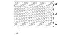
- the graphene joint in the present embodiment is a heat conductive plate 20 having a structure in which a metal plate is joined as a member to be joined to a graphene-containing carbonaceous member containing a graphene aggregate.
- the power module 1 shown in FIG. 1 includes an insulating circuit board 10, a semiconductor element 3 bonded to one surface side (upper side in FIG. 1) of the insulating circuit board 10 via a solder layer 2, and an insulating circuit board 10.
- a heat conductive plate 20 arranged on the other surface side (lower side in FIG. 1) and a heat sink 31 arranged on the other surface side of the heat conductive plate 20 are provided.
- the insulating circuit board 10 is arranged on the insulating layer 11, the circuit layer 12 arranged on one surface of the insulating layer 11 (upper surface in FIG. 1), and the other surface of the insulating layer 11 (lower surface in FIG. 1). It is provided with the provided metal layer 13.
- the insulating layer 11 prevents electrical connection between the circuit layer 12 and the metal layer 13.
- the insulating layer 11 has highly insulating aluminum nitride (AlN) and aluminum oxide (Al 2 O 3 ). , Silicon nitride (Si 3 N 4 ) and other ceramics.
- the thickness of the insulating layer 11 is set within the range of 0.2 to 1.5 mm, and in the present embodiment, it is set to 0.635 mm.
- the circuit layer 12 is formed by joining a metal plate having excellent conductivity to one surface of the insulating layer 11.
- a metal plate constituting the circuit layer 12 a copper plate made of copper or a copper alloy, specifically, a rolled plate of oxygen-free copper is used.
- a circuit pattern is formed in the circuit layer 12, and one surface (upper surface in FIG. 1) is a mounting surface on which the semiconductor element 3 is mounted.
- the thickness of the metal plate (copper plate) to be the circuit layer 12 is set within the range of 0.1 mm or more and 1.0 mm or less, and in the present embodiment, it is set to 0.6 mm.
- the method of joining the metal plate (copper plate) to be the circuit layer 12 and the insulating layer 11 is not particularly limited, and can be joined using an active metal brazing material or the like.
- the metal layer 13 is formed by joining a metal plate having excellent thermal conductivity to the other surface of the insulating layer 11.
- a copper plate made of copper or a copper alloy specifically, a rolled plate of oxygen-free copper is used.
- the thickness of the metal plate (copper plate) to be the metal layer 13 is set within the range of 0.1 mm or more and 1.0 mm or less, and in the present embodiment, it is set to 0.6 mm.
- the method of joining the metal plate (copper plate) to be the metal layer 13 and the insulating layer 11 is not particularly limited, and can be joined using an active metal brazing material or the like.
- the heat sink 31 is for cooling the above-mentioned insulating circuit board 10, and has a structure in which a plurality of flow paths 32 for flowing a cooling medium (for example, cooling water) are provided.
- the heat sink 31 is preferably made of a material having good thermal conductivity, for example, aluminum or an aluminum alloy, copper or a copper alloy, and in this embodiment, it is made of oxygen-free copper.
- the semiconductor element 3 is made of a semiconductor material such as Si or SiC.
- the semiconductor element 3 is mounted on the circuit layer 12 via, for example, a solder layer 2 made of a Sn—Ag-based, Sn—In-based, or Sn—Ag—Cu-based solder material.
- the graphene junction (heat conductive plate 20) of the present embodiment is interposed between the insulating circuit board 10 and the heat sink 31.
- the outermost layers of both main surfaces of the heat conductive plate 20 are made of oxygen-free copper
- the metal layer 13 of the insulating circuit substrate 10 made of copper and the heat sink 31 made of copper are, for example, Sn-. It is joined via an Ag-based, Sn-In-based, or Sn-Ag-Cu-based solder material.
- the heat conductive plate 20 of the present embodiment has a carbon plate 21 made of a graphene-containing carbonaceous member containing a graphene aggregate and a metal member joined to both main surfaces of the carbon plate 21. Layer 25 and.
- the graphene-containing carbonaceous member constituting the carbon plate 21 contains graphene aggregates formed by depositing single-layer or multi-layer graphene and flat graphite particles so that the flat graphite particles fold their basal surfaces.
- the graphene aggregate has a laminated structure as a binder.
- the flat graphite particles have a basal surface on which a carbon hexagonal network surface appears and an edge surface on which an end portion of the carbon hexagonal network surface appears.
- the flat graphite particles scaly graphite, scaly graphite, earthy graphite, flaky graphite, kiss graphite, pyrolytic graphite, highly oriented pyrolytic graphite and the like can be used.
- the average particle size of the graphite particles as seen from the basal surface is preferably in the range of 10 ⁇ m or more and 1000 ⁇ m or less, and more preferably in the range of 50 ⁇ m or more and 800 ⁇ m or less. By setting the average particle size of the graphite particles within the above range, the thermal conductivity is improved.
- the thickness of the graphite particles is preferably in the range of 1 ⁇ m or more and 50 ⁇ m or less, and more preferably in the range of 1 ⁇ m or more and 20 ⁇ m or less. By setting the thickness of the graphite particles within the above range, the orientation of the graphite particles is appropriately adjusted.
- the thickness of the graphite particles is preferably in the range of 1/1000 to 1/2 of the particle size seen from the basal surface. By setting the thickness of the graphite particles within the above range, excellent thermal conductivity and orientation of the graphite particles can be appropriately adjusted.
- the graphene aggregate is a deposit of single-layer or multi-layer graphene, and the number of layers of the multi-layer graphene is, for example, 100 layers or less, preferably 50 layers or less.
- This graphene aggregate can be produced, for example, by dropping a graphene dispersion in which single-layer or multi-layer graphene is dispersed in a solvent containing lower alcohol or water onto a filter paper and depositing the graphene while separating the solvent. It is possible.
- the average particle size of the graphene aggregate is preferably in the range of 1 ⁇ m or more and 1000 ⁇ m or less. By keeping the average particle size of the graphene aggregate within the above range, the thermal conductivity is improved.
- the thickness of the graphene aggregate is preferably in the range of 0.05 ⁇ m or more and less than 50 ⁇ m. By keeping the thickness of the graphene aggregate within the above range, the strength of the carbonaceous member is ensured.
- the thickness of the carbon plate 21 is preferably in the range of 0.3 mm or more and 3 mm.
- the metal member layer 25 is formed by joining a metal plate to the main surface of the carbon plate 21.
- the metal plate constituting the metal member layer 25 is preferably made of a metal having excellent thermal conductivity, and the metal plate of the present embodiment is made of copper or a copper alloy, more specifically. , It is said to be a rolled plate of oxygen-free copper.
- the thickness of the metal member layer 25 is preferably 50 ⁇ m or more, and more preferably 100 ⁇ m or more.
- the thickness of the metal member layer 25 (thickness of the metal plate) is preferably 5000 ⁇ m or less, and more preferably 3000 ⁇ m or less.
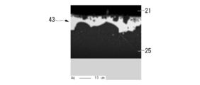
- FIG. 3 shows an observation photograph of the bonding interface between the carbon plate 21 made of graphene-containing carbonaceous member and the metal member layer 25
- FIG. 4 shows the joining of the carbon plate 21 made of graphene-containing carbonaceous member and the metal member layer 25.
- the element mapping diagram of the interface is shown.
- the upper black portion is the carbon plate 21 (graphene-containing carbonaceous member)
- the gray portion located below the carbon plate 21 is the metal member layer 25 (joint member).
- the active metal oxide and the activity are formed on the bonding surface of the carbon plate 21.
- An active metal compound layer 41 containing one or two metal carbides is formed.
- the region where the active metal (Ti) is present is the active metal compound layer 41.
- a Sn-enriched layer 42 having a Sn concentration of 1 mass% or more is formed on the carbon plate 21 side of the bonding interface 40.
- the Sn-enriched region is the Sn-enriched layer 42.
- An alloy layer 43 containing Ag and Cu is formed on the metal member layer 25 side of the bonding interface 40.
- the region where Ag and Cu coexist is the alloy layer 43.
- the active metal compound layer 41 is formed by reacting the active metal contained in the bonding material interposed between the carbon plate 21 and the metal plate with oxygen and carbon at the time of bonding.
- the active metal constituting the active metal compound layer 41 for example, one kind or two or more kinds selected from Ti, Zr, Hf, and Nb can be used.
- the active metal is Ti
- the active metal compound layer 41 contains one or two types of titanium oxide (Ti—O) and titanium carbide (Ti—C). ..
- the thickness t1 of the active metal compound layer 41 is 0.05 ⁇ m or more, the reaction between the bonding material and the carbon plate 21 is promoted, and the bonding strength of the carbon plate 21 is sufficiently secured.
- the thickness t1 of the active metal compound layer 41 is 3 ⁇ m or less, the occurrence of cracks in the active metal compound layer 41 can be suppressed when the active metal compound layer 41 is loaded. Therefore, in the present embodiment, the thickness t1 of the active metal compound layer 41 is set to be within the range of 0.05 ⁇ m or more and 3 ⁇ m or less.
- the thickness t1 of the active metal compound layer 41 is more preferably 0.1 ⁇ m or more, and even more preferably 0.2 ⁇ m or more.
- the thickness t1 of the active metal compound layer 41 is more preferably 2 ⁇ m or less, and more preferably 1.8 ⁇ m or less.
- the Sn concentrated layer 42 is formed by segregating Sn contained in the bonding material interposed between the carbon plate 21 and the metal plate toward the carbon plate 21 at the time of bonding.
- Sn concentrated layer 42 a cross-sectional observation sample near the interface of the graphene / ceramics joint was taken, and EPMA (for example, JXA-8530F manufactured by JEOL Ltd., acceleration voltage: 15 kV, spot diameter: 1 ⁇ m or less) was used. It can be specified by acquiring the EPMA mapping.
- the thickness t2 of the Sn concentrated layer 42 is 0.2 ⁇ m or more, the reliability of the thermal cycle can be reliably improved.
- the thickness t2 of the Sn-concentrated layer 42 is limited to 10 ⁇ m or less, it is possible to suppress the occurrence of cracks in the Sn-concentrated layer 42 when a cold cycle load is applied. Therefore, in the present embodiment, the thickness t2 of the Sn concentrated layer 42 is preferably in the range of 0.2 ⁇ m or more and 10 ⁇ m or less.
- the thickness t2 of the Sn concentrated layer 42 is more preferably 0.5 ⁇ m or more, and more preferably 0.7 ⁇ m or more.
- the thickness t2 of the Sn concentrated layer 42 is more preferably 5 ⁇ m or less, and more preferably 3 ⁇ m or less.
- the alloy layer 43 is formed by the reaction of Ag and Cu contained in the bonding material interposed between the carbon plate 21 and the metal plate at the time of bonding.
- the metal member layer 25 metal plate
- the alloy layer 43 is formed by diffusing Ag of the bonding material on the metal member layer 25 (metal plate) side. .. Therefore, in the alloy layer 43 and the metal member layer 25, there is a concentration gradient of Ag. When Ag is sufficiently diffused to the metal member layer 25 side and solid-solved in the metal member layer 25, the alloy layer 43 may not be formed.
- the thickness t3 of the alloy layer 43 is 1 ⁇ m or more, the reaction of the bonding material is sufficiently promoted, and the bonding strength between the carbon plate 21 and the metal member layer 25 is sufficiently secured.
- the thickness t3 of the alloy layer 43 is 20 ⁇ m or less, it is possible to suppress the occurrence of cracks in the alloy layer 43 during a cold cycle load. Therefore, in the present embodiment, the thickness t3 of the alloy layer 43 is preferably in the range of 1 ⁇ m or more and 20 ⁇ m or less.
- the thickness t3 of the alloy layer 43 is more preferably 2 ⁇ m or more, and more preferably 3 ⁇ m or more.
- the thickness t3 of the alloy layer 43 is more preferably 10 ⁇ m or less, and more preferably 8 ⁇ m or less.
- Carbon plate forming step S01 First, the above-mentioned flat graphite particles and graphene aggregates are weighed so as to have a predetermined blending ratio, and these are mixed by an existing mixing device such as a ball mill. A molded product is obtained by filling the obtained mixture in a mold having a predetermined shape and pressurizing the mixture. Heating may be performed during pressurization. Then, the obtained molded product is cut out to obtain a carbon plate 21.
- the pressure at the time of molding is preferably in the range of 20 MPa or more and 1000 MPa or less, and more preferably in the range of 100 MPa or more and 300 MPa or less.
- the temperature at the time of molding is preferably in the range of 50 ° C. or higher and 300 ° C. or lower.
- the pressurization time is preferably in the range of 0.5 minutes or more and 10 minutes or less.
- a metal plate to be a metal member layer 25 is laminated on both main surfaces of the carbon plate 21 via a bonding material.
- a bonding material a material containing Ag, Cu, Sn, and an active metal (Ti in this embodiment) is used.
- the bonding material may be in the form of a paste or in the form of a foil. Further, for example, a Cu—Ag—Sn alloy and an active metal may be laminated.
- the bonding material contains Cu in the range of 18 mass% or more and 34 mass% or less, Sn in the range of 3 mass% or more and 10 mass% or less, Ti in the range of 0.3 mass% or more and 7 mass% or less, and the balance is Ag and The composition used as an unavoidable impurity is used.
- Metal plate joining step S03 Next, the metal plate and the carbon plate 21 laminated via the bonding material are pressed in the stacking direction, heated, and then cooled to join the metal plate and the carbon plate 21 to form the metal member layer 25.
- the heating temperature is preferably in the range of 740 ° C. or higher and 900 ° C. or lower.
- the holding time at the heating temperature is preferably in the range of 20 minutes or more and 180 minutes or less.
- the pressurizing pressure is preferably in the range of 0.1 MPa or more and 3.5 MPa or less.
- the atmosphere is preferably a non-oxidizing atmosphere such as a reduced pressure atmosphere or a nitrogen gas atmosphere.
- the active metal (Ti in the present embodiment) contained in the joining material reacts with oxygen and carbon, so that the active metal compound layer 41 is formed on the joining surface of the carbon plate 21.
- the Sn-concentrated layer 42 is formed by segregating Sn contained in the bonding material toward the carbon plate 21 side.
- the alloy layer 43 is formed on the metal member layer 25 side by reacting Cu and Ag contained in the bonding material and diffusing Ag on the metal plate (metal member layer 25) side.
- the graphene joint (heat conductive plate 20) of the present embodiment is manufactured.
- the active metal oxide is formed on the joint surface of the carbon plate 21 at the joint interface between the carbon plate 21 and the metal member layer 25. Since the active metal compound layer 41 containing one or two of (Ti-O) and the active metal carbide (Ti-C) is formed, the graphene-containing carbonaceous member is made of the active metal (Ti in this embodiment). The joint surface of the carbon plate 21 made of the carbon plate 21 is sufficiently reacted, and the carbon plate 21 and the metal member layer 25 (metal plate) are firmly joined.
- Sn contained in the bonding material is segregated on the carbon plate 21 side to form a Sn-enriched layer 42 having a Sn concentration of 1 mass% or more. Therefore, it is possible to prevent the carbon plate 21 and the metal member layer 25 from peeling off when a cold cycle load is applied, and it is possible to improve the reliability of the cold cycle. Since a bonding material containing Sn is used, the carbon plate 21 and the metal member layer 25 (metal plate) can be firmly bonded under relatively low temperature conditions.
- the thickness of the active metal compound layer 41 is 0.05 ⁇ m or more, it is possible to firmly join the carbon plate 21 made of a graphene-containing carbonaceous member and the metal member layer 25. Become.
- the thickness of the active metal compound layer 41 is limited to 3 ⁇ m or less, it is possible to suppress the occurrence of cracks in the active metal compound layer 41 when loaded with a cold cycle.
- the thickness of the Sn concentrated layer 42 when the thickness of the Sn concentrated layer 42 is 0.2 ⁇ m or more, the reliability of the thermal cycle can be reliably improved.
- the thickness of the Sn-concentrated layer 42 when the thickness of the Sn-concentrated layer 42 is limited to 10 ⁇ m or less, it is possible to suppress the occurrence of cracks in the Sn-concentrated layer 42 when a cold cycle load is applied.
- the graphene-containing carbonaceous member constituting the carbon plate 21 contains a graphene aggregate formed by depositing single-layer or multi-layer graphene and flat graphite particles, and the flat graphite particles are formed.
- the carbon plate 21 graphene-containing carbon
- the heat conductive plate 20 is arranged between the insulating circuit board 10 and the heat sink 31, the insulating circuit is formed in the metal member layer 25 formed on one main surface side of the heat conductive plate 20.
- the heat from the substrate 10 can be spread in the plane direction, the heat can be efficiently transferred in the thickness direction, and the heat can be dissipated in the heat sink 31. Therefore, the power module 1 having excellent heat dissipation characteristics can be configured.
- the graphene junction in the present embodiment is an insulating substrate 120 having a structure in which a ceramic plate is bonded as a member to be bonded to a graphene-containing carbonaceous member containing a graphene aggregate.
- the ceramic plate 125 and the carbon plate 121 made of a graphene-containing carbonaceous member containing a graphene aggregate are bonded to both sides of the ceramic plate 125, respectively. It is said to have a structure.
- the graphene-containing carbonaceous member constituting the carbon plate 121 contains graphene aggregates formed by depositing single-layer or multi-layer graphene and flat graphite particles, and is flat graphite. It is preferable that the particles have a structure in which graphene aggregates are laminated as a binder so that their basal surfaces overlap.
- the thickness of the carbon plate 121 is preferably in the range of 0.3 mm or more and 3 mm.
- the ceramic plate 125 is made of ceramics having excellent insulating properties, for example, aluminum nitride (AlN), aluminum oxide (Al 2 O 3 ), silicon nitride (Si 3 N 4 ), and the like.
- the thickness of the ceramic plate 125 is preferably 100 ⁇ m or more, and more preferably 250 ⁇ m or more.
- the ceramic plate 125 is preferably 1500 ⁇ m or less, and more preferably 1000 ⁇ m or less.
- FIG. 7 shows an observation photograph of the bonding interface between the carbon plate 121 made of a graphene-containing carbonaceous member and the ceramic plate 125.
- the upper black portion is the carbon plate 121 (graphene-containing carbonaceous member)
- the gray portion located below the carbon plate 121 is the ceramic plate 125 (joint member).
- one kind of active metal oxide and active metal carbide is formed on the bonding surface of the carbon plate 121 as in the first embodiment.
- an active metal compound layer containing two types is formed.
- a Sn-enriched layer having a Sn concentration of 1 mass% or more is formed on the carbon plate 121 side of the bonding interface 140.
- An alloy layer containing Ag and Cu is formed on the ceramic plate 125 side of the bonding interface 140.
- the active metal compound layer is formed by reacting the active metal (Ti in this embodiment) contained in the bonding material interposed between the carbon plate 121 and the ceramic plate 125 at the time of bonding with oxygen and carbon.
- the active metal compound layer in the present embodiment has the same structure as that in the first embodiment.
- the thickness t11 of the active metal compound layer is in the range of 0.05 ⁇ m or more and 3 ⁇ m or less.
- the Sn-enriched layer is formed by segregating Sn contained in the bonding material interposed between the carbon plate 121 and the ceramic plate 125 toward the carbon plate 121 at the time of bonding.
- the Sn-enriched layer in this embodiment has the same structure as that in the first embodiment.
- the thickness t12 of the Sn concentrated layer is preferably in the range of 0.2 ⁇ m or more and 10 ⁇ m or less.
- the alloy layer is formed by the reaction of Ag and Cu contained in the bonding material interposed between the carbon plate 121 and the ceramic plate 125 at the time of bonding.
- Ag of the bonding material does not diffuse to the ceramic plate 125 side, and the alloy layer tends to be formed thicker than that of the first embodiment.
- the thickness t13 of the alloy layer is preferably in the range of 1 ⁇ m or more and 20 ⁇ m or less.
- the thickness t13 of the alloy layer is more preferably 2 ⁇ m or more, and more preferably 3 ⁇ m or more.
- the thickness t13 of the alloy layer is more preferably 10 ⁇ m or less, and more preferably 8 ⁇ m or less.
- the flat graphite particles and the graphene aggregate are weighed so as to have a predetermined blending ratio, and this is mixed by an existing mixing device such as a ball mill, and the obtained mixture is obtained. Is filled in a mold having a predetermined shape and pressed to form a molded product, and the obtained molded product is cut out.
- the graphene aggregate formed by depositing single-layer or multi-layer graphene and the flat graphite particles are included, and the flat graphite particles are laminated with the graphene aggregate as a binder so that the basal surfaces thereof are folded. Therefore, it is possible to obtain a graphene-containing carbonaceous member (carbon plate 121) having a structure in which the basal surface of the flat-shaped graphite particles is oriented in one direction.
- the carbon plate 121 is laminated on both main surfaces of the ceramic plate 125 via a bonding material.
- a bonding material a material containing Ag, Cu, Sn, and an active metal (Ti in this embodiment) is used as in the first embodiment.
- the heating temperature is preferably in the range of 750 ° C. or higher and 900 ° C. or lower.
- the holding time at the heating temperature is preferably in the range of 20 minutes or more and 180 minutes or less.
- the pressurizing pressure is preferably in the range of 0.1 MPa or more and 3.5 MPa or less.
- the atmosphere is preferably a non-oxidizing atmosphere such as a reduced pressure atmosphere or a nitrogen gas atmosphere.
- the active metal (Ti in the present embodiment) contained in the joining material reacts with oxygen and carbon to form an active metal compound layer on the joining surface of the carbon plate 121.
- the Sn contained in the bonding material segregates toward the carbon plate 121 side to form a Sn concentrated layer.
- An alloy layer is formed on the ceramic plate 125 side by the reaction between Cu and Ag contained in the bonding material.
- the graphene junction (insulated substrate 120) according to the present embodiment is manufactured.
- an active metal compound layer is formed on the joint surface of the carbon plate 121 at the joint interface between the carbon plate 121 and the ceramic plate 125. Therefore, the bonding surface of the carbon plate 121 made of the graphene-containing carbonaceous member is sufficiently reacted by the active metal (Ti in the present embodiment), and the carbon plate 121 and the ceramic plate 125 are firmly bonded. ..
- the thickness t11 of the active metal compound layer is 0.05 ⁇ m or more, it is possible to firmly join the carbon plate 121 made of the graphene-containing carbonaceous member and the ceramic plate 125. ..
- the thickness t11 of the active metal compound layer is limited to 3 ⁇ m or less, it is possible to suppress the occurrence of cracks in the active metal compound layer when loaded with a cold cycle.
- the thickness t12 of the Sn concentrated layer when the thickness t12 of the Sn concentrated layer is 0.2 ⁇ m or more, the reliability of the thermal cycle can be reliably improved.
- the thickness t12 of the Sn-concentrated layer is limited to 10 ⁇ m or less, it is possible to suppress the occurrence of cracks in the Sn-concentrated layer when a cold cycle load is applied.
- the graphene-containing carbonaceous member constituting the carbon plate 121 contains a graphene aggregate formed by depositing single-layer or multi-layer graphene and flat graphite particles, and the flat graphite particles are formed.
- the carbon plate 121 graphene-containing carbon
- the insulating substrate 120 of the present embodiment includes the ceramic plate 125, it has excellent insulating properties. Since it is provided with a carbon plate 121 made of a graphene-containing carbonaceous member, it has excellent thermal conductivity. Therefore, for example, it can be used as the insulating layer 11 of the power module 1 (insulated circuit board 10) shown in FIG.
- a semiconductor element (power semiconductor element) is mounted on the circuit layer of the insulated circuit board to form a power module, but the present embodiment is not limited to this.
- an LED element may be mounted on an insulated circuit board to form an LED module
- a thermoelectric element may be mounted on a circuit layer of an insulated circuit board to form a thermoelectric module.
- the power module 1 having a structure in which the heat conductive plate 20 is arranged between the insulating circuit board 10 and the heat sink 31 has been described as an example, but the present invention is limited to this. There is no particular limitation on the method of using the graphene conjugate of the present invention.
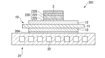
- the power module 201 has a structure in which the heat conductive plate 220 is arranged between the circuit layer 12 of the insulating circuit board 10 and the semiconductor element 3. Good.
- the power module 301 using the heat conductive plate 320 may be used as the metal layer of the insulating circuit board 310.
- the power module 401 using the heat conductive plate 420 may be used as the circuit layer and the metal layer of the insulating circuit board 410.
- the power module 201 shown in FIG. 9 is different from the power module 1 shown in FIG. 1 in that a heat conductive plate 220 is used instead of the solder layer 2 and a solder layer 204 is used instead of the heat conductive plate 20.
- a heat conductive plate 220 is used instead of the solder layer 2 and a solder layer 204 is used instead of the heat conductive plate 20.
- Other configurations are the same as those of the power module 1 shown in FIG. 1, and the same reference numerals are given to the same configurations, and the description thereof will be omitted.
- the heat conductive plate 220 includes a carbon plate 221 made of a graphene-containing carbonaceous member containing a graphene aggregate, and a metal member layer 225 joined to both main surfaces of the carbon plate 221.
- the heat conductive plate 220, the carbon plate 221 and the metal member layer 225 have the same configurations as the heat conductive plate 20, the carbon plate 21 and the metal member layer 25 of the first embodiment, respectively.
- the metal layer 13 and the heat sink 31 are joined via a solder layer 204 made of, for example, a Sn—Ag-based, Sn—In-based, or Sn—Ag—Cu-based solder material.
- the heat conductive plate 220 is arranged between the circuit layer 12 of the insulating circuit board 10 and the semiconductor element 3, the heat from the semiconductor element 3 can be spread in the plane direction, and this heat can be spread. Is efficiently transmitted in the thickness direction, and heat can be dissipated in the heat sink 31. Therefore, the power module 201 having excellent heat dissipation characteristics can be configured.
- the power module 301 shown in FIG. 10 is an insulating circuit board 310 in which a carbon plate 321 is used as a metal layer instead of the metal layer 13, and the insulating circuit board 310 and the heat sink 31 are joined by using an active metal brazing material or the like.
- the point is different from the power module 1 shown in FIG.
- Other configurations are the same as those of the power module 1 shown in FIG. 1, and the same reference numerals are given to the same configurations, and the description thereof will be omitted.
- the carbon plate 321 has the same configuration as the carbon plate 21 of the first embodiment or the carbon plate 121 of the second embodiment.
- the insulating layer 11 and the carbon plate 321 are joined in the same configuration as the second graphene joint (insulating substrate 120).
- the carbon plate 321 and the heat sink 31 are joined in the same configuration as the first graphene joint (heat conductive plate 20).
- a carbon plate 321 is used as the metal layer of the insulating circuit board 310, and the insulating layer 11 and the carbon plate 321 are joined in the same configuration as the second graphene junction (insulating substrate 120), and carbon is used. Since the plate 321 and the heat sink 31 are joined in the same configuration as the first graphene joint (heat conductive plate 20), the heat from the insulating circuit board 10 can be spread in the plane direction, and this heat can be dissipated. It can be efficiently transmitted in the thickness direction and dissipated in the heat sink 31. Therefore, the power module 301 having excellent heat dissipation characteristics can be configured.
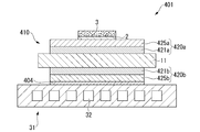
- the power module 401 shown in FIG. 11 is an insulating circuit board 410 in which a heat conductive plate 420a is used as a circuit layer instead of the circuit layer 12, and a heat conductive plate 420b is used as a metal layer instead of the metal layer 13. It differs from the power module 1 shown in FIG. 1 in that the solder layer 404 is used instead of the plate 20.
- Other configurations are the same as those of the power module 1 shown in FIG. 1, and the same reference numerals are given to the same configurations, and the description thereof will be omitted.
- the heat conductive plate 420a includes a carbon plate 421a made of a graphene-containing carbonaceous member containing a graphene aggregate, and a metal member layer 425a joined to one surface side (upper side of FIG. 11) of the carbon plate 421a. I have.
- the heat conductive plate 420a, the carbon plate 421a, and the metal member layer 425a have the same configurations as the heat conductive plate 20, the carbon plate 21, and the metal member layer 25 of the first embodiment, respectively.
- the heat conductive plate 420b includes a carbon plate 421b made of a graphene-containing carbonaceous member containing a graphene aggregate, and a metal member layer 425b joined to the other surface side (lower side of FIG.
- the heat conductive plate 420b, the carbon plate 421b, and the metal member layer 425b have the same configurations as the heat conductive plate 20, the carbon plate 21, and the metal member layer 25 of the first embodiment, respectively.
- the carbon plate 421a and the insulating layer 11, and the insulating layer 11 and the carbon plate 421b are each joined in the same configuration as the second graphene joint (insulating substrate 120).
- the heat conductive plate 420b and the heat sink 31 are joined via a solder layer 404 made of, for example, a Sn—Ag-based, Sn—In-based, or Sn—Ag—Cu-based solder material.
- the heat conductive plate 420a is used as a circuit layer
- the heat conductive plate 420b is used as a metal layer
- the carbon plate 421a and the insulating layer 11 and the insulating layer 11 and the carbon plate 421b are each a second graphene joint. Since they are joined in the same configuration as (insulated substrate 120), heat from the semiconductor element 3 and the insulating circuit board 410 can be spread in the plane direction, and this heat is efficiently transferred in the thickness direction to heat sink 31. Can dissipate heat in. Therefore, the power module 401 having excellent heat dissipation characteristics can be configured.
- the flat graphite particles and the graphene aggregate are mixed at a predetermined compounding ratio, mixed, and heated by pressure to form the flat graphite particles on the basal surface thereof.
- a molded body having a structure in which graphene aggregates were laminated as a binder was obtained so as to be folded over.
- the obtained molded product was cut out to obtain a carbon plate (40 mm ⁇ 40 mm ⁇ thickness 1.5 mm).
- a copper plate (40 mm ⁇ 40 mm) made of rolled oxygen-free copper is interposed on one surface of this carbon plate via a bonding material (thickness variation) having a composition of Ag-28 mass% Cu-5 mass% Sn-3 mass% Ti. ⁇ Thickness 0.3 mm) or ceramic plate (40 mm ⁇ 40 mm ⁇ thickness 0.3 mm) was laminated, and the carbon plate and the copper plate were joined under the conditions shown in Table 1. Then, the bonding interface between the carbon plate and the copper plate was observed, and the thickness of the active metal compound layer and the thickness of the Sn concentrated layer were confirmed.
- the thickness of the active metal compound layer is determined by collecting an observation sample from the central part of the graphene / copper junction and scanning the junction interface with a scanning transmission electron microscope (FEI Titan ChemiSTEM (with EDS detector)). Observation was performed under the conditions of a magnification of 40,000 times and an acceleration voltage of 200 kV, and mapping was performed using an energy dispersive X-ray analysis method (NSS7 manufactured by Thermo Scientific Co., Ltd.) to determine the area of the region where the active metal exists. The measurement was performed, the value divided by the width of the measurement field was obtained, and the average value of the five fields was taken as the thickness of the active metal compound layer. As measurement points, a total of 5 points were observed, which are the region of the center point of the insulated circuit board and the region of four vertices of a 20 mm ⁇ 20 mm quadrangle centered on that point.
- a cross-sectional observation sample near the bonding interface of the graphene / copper junction was collected, and EPMA (JXA-8530F manufactured by JEOL Ltd., acceleration voltage: 15 kV, spot diameter: 1 ⁇ m or less) was applied.
- EPMA mapping was obtained using EPMA mapping, the area where Sn was 1 mass% or more was regarded as a Sn-enriched layer, the area was measured, the value divided by the width of the measurement field was obtained, and the average value of the five fields was Sn-concentrated.
- the thickness of the chemical layer was used. As measurement points, a total of 5 points were observed, which are the region of the center point of the insulated circuit board and the region of four vertices of a 20 mm ⁇ 20 mm quadrangle centered on that point.
- the obtained conjugate was loaded with 2000 cycles of a cold heat cycle of ⁇ 55 ° C. ⁇ 30 minutes ⁇ ⁇ 175 ° C. ⁇ 30 minutes. Then, the bonding ratio at the interface between the carbon plate and the copper plate was evaluated using an ultrasonic flaw detector (FineSAT200 manufactured by Hitachi Power Solutions, Ltd.) and calculated from the following formula.
- the initial joining area was defined as the area to be joined before joining. In the image obtained by binarizing the ultrasonic flaw detection image, the peeling is shown by the white part in the joint portion, and therefore the area of this white part is defined as the peeling area (non-joint part area).
- (Joining ratio) ⁇ (Initial joining area)-(Non-joining area) ⁇ / (Initial joining area) x 100
- Example 1-6 of the present invention in which the Sn-concentrated layer was formed and the thickness of the active metal compound layer was in the range of 0.05 ⁇ m or more and 3 ⁇ m or less, the bonding ratio after the thermal cycle test was high. It was 80% or more, and the thermal cycle reliability was excellent.
- the material to be bonded and the graphene-containing carbonaceous member containing the graphene aggregate are firmly bonded, and peeling does not occur even under a cold cycle load. It was confirmed that it is possible to provide a graphene conjugate having excellent thermal cycle reliability.
- the material to be bonded and the graphene-containing carbonaceous member containing the graphene aggregate are firmly bonded to each other, peeling does not occur even under a cold cycle load, and the cold cycle reliability is excellent.
- Graphene conjugates can be provided.
Landscapes
- Chemical & Material Sciences (AREA)
- Engineering & Computer Science (AREA)
- Organic Chemistry (AREA)
- Materials Engineering (AREA)
- Ceramic Engineering (AREA)
- Physics & Mathematics (AREA)
- Inorganic Chemistry (AREA)
- Condensed Matter Physics & Semiconductors (AREA)
- General Physics & Mathematics (AREA)
- Computer Hardware Design (AREA)
- Microelectronics & Electronic Packaging (AREA)
- Power Engineering (AREA)
- Nanotechnology (AREA)
- Structural Engineering (AREA)
- Cooling Or The Like Of Semiconductors Or Solid State Devices (AREA)
Abstract
このグラフェン接合体(20)は、グラフェン集合体を含有するグラフェン含有炭素質部材(21)と被接合部材(25)とが接合された構造を有し、グラフェン含有炭素質部材(21)と被接合部材(25)との接合界面(40)においては、グラフェン含有炭素質部材(21)の接合面に、活性金属酸化物及び活性金属炭化物の1種又は2種を含む活性金属化合物層(41)が形成されるとともに、グラフェン含有炭素質部材(21)側に、Sn濃度が1mass%以上であるSn濃化層(42)が形成されている。
Description
この発明は、グラフェン集合体を含有するグラフェン含有炭素質部材と被接合部材とが接合された構造のグラフェン接合体に関する。
本願は、2019年11月25日に、日本に出願された特願2019-212090号、及び、2020年11月16日に、日本に出願された特願2020-190318号に基づき優先権を主張し、その内容をここに援用する。
本願は、2019年11月25日に、日本に出願された特願2019-212090号、及び、2020年11月16日に、日本に出願された特願2020-190318号に基づき優先権を主張し、その内容をここに援用する。
グラフェン集合体を含有するグラフェン含有炭素質部材は、熱伝導性に優れていることから、放熱部材及び熱伝導部材を構成する部材として特に適している。
例えば、上述のグラフェン集合体を含有するグラフェン含有炭素質部材の表面にセラミックス等からなる絶縁層を形成することにより、絶縁基板として使用することが可能となる。
例えば、上述のグラフェン集合体を含有するグラフェン含有炭素質部材の表面にセラミックス等からなる絶縁層を形成することにより、絶縁基板として使用することが可能となる。
グラフェン含有炭素質部材の表面に金属層を形成することにより、熱伝導板として使用することが可能となる。この熱伝導板は、例えば、パワーモジュール及びLEDモジュール等のように、発熱体(パワー半導体素子及びLED素子)を搭載する各種装置において、これらの発熱体(素子、及び、素子を搭載した基板等)とヒートシンクとの間に配設される。
例えば特許文献1には、第1方向に沿ってグラフェンシートが積層された構造体と、第1方向と交差する第2方向における上記構造体の端面に接合される中間部材(金属又はセラミックス)と、を有し、この中間部材(金属又はセラミックス)が、少なくともチタンを含むインサート材を介して、上記端面に加圧接合された異方性熱伝導素子が開示されている。
上述の絶縁基板においては、使用環境下において冷熱サイクルが負荷されることがある。特に、最近では、エンジンルーム等の過酷な環境下で使用されることがあり、温度差が大きな厳しい条件の冷熱サイクルが負荷されることがある。
上述の特許文献1においては、金属又はセラミックスからなる中間部材とグラフェンの構造体を、チタンを含むインサート材を介して接合しているが、接合条件によっては、金属又はセラミックスからなる中間部材とグラフェンの構造体とを強固に接合することができず、厳しい条件の冷熱サイクルが負荷された際に剥離が生じるおそれがあった。
上述の特許文献1においては、金属又はセラミックスからなる中間部材とグラフェンの構造体を、チタンを含むインサート材を介して接合しているが、接合条件によっては、金属又はセラミックスからなる中間部材とグラフェンの構造体とを強固に接合することができず、厳しい条件の冷熱サイクルが負荷された際に剥離が生じるおそれがあった。
この発明は、前述した事情に鑑みてなされたものであって、被接合材とグラフェン集合体を含有するグラフェン含有炭素質部材とが強固に接合されており、冷熱サイクル負荷時においても剥離が生じることがなく、冷熱サイクル信頼性に優れたグラフェン接合体を提供することを目的とする。
このような課題を解決して、前記目的を達成するために、本発明の一態様に係るグラフェン接合体は、グラフェン集合体を含有するグラフェン含有炭素質部材と被接合部材とが接合された構造のグラフェン接合体であって、前記グラフェン含有炭素質部材と前記被接合部材との接合界面においては、前記グラフェン含有炭素質部材の接合面に、活性金属化合物層が形成されるとともに、前記グラフェン含有炭素質部材側に、Sn濃度が1mass%以上とされたSn濃化層が形成されており、前記活性金属化合物層の厚さが0.05μm以上3μm以下の範囲内とされていることを特徴としている。
この構成のグラフェン接合体においては、前記グラフェン含有炭素質部材と前記被接合部材との接合界面において、前記グラフェン含有炭素質部材の接合面に、活性金属酸化物及び活性金属炭化物の1種又は2種を含む活性金属化合物層が形成されているので、活性金属によってグラフェン含有炭素質部材の接合面が十分に反応しており、グラフェン含有炭素部材と被接合部材とを強固に接合することができる。
そして、前記グラフェン含有炭素質部材と前記被接合部材との接合界面において、前記グラフェン含有炭素質部材側に、Sn濃度が1mass%以上とされたSn濃化層が形成されているので、冷熱サイクル負荷時に前記グラフェン含有炭素質部材と前記被接合部材とが剥離することを抑制でき、冷熱サイクル信頼性を向上させることができる。
また、Snを含む接合材を用いるので、比較的低温条件で、前記グラフェン含有炭素質部材と前記被接合部材とを強固に接合することが可能となる。
前記活性金属化合物層の厚さが0.05μm以上とされているので、前記グラフェン含有炭素質部材と前記被接合部材とをさらに強固に接合することが可能となる。一方、前記活性金属化合物層の厚さが3μm以下に制限されているので、冷熱サイクル負荷時に活性金属化合物層におけるクラックの発生を抑制することができる。
本発明の一態様に係るグラフェン接合体においては、前記Sn濃化層の厚さが0.2μm以上10μm以下の範囲内とされていることが好ましい。
この場合、前記Sn濃化層の厚さが0.2μm以上とされているので、冷熱サイクル信頼性をさらに向上させることができる。一方、前記Sn濃化層の厚さが10μm以下に制限されているので、冷熱サイクル負荷時にSn濃化層におけるクラックの発生を抑制することができる。
この場合、前記Sn濃化層の厚さが0.2μm以上とされているので、冷熱サイクル信頼性をさらに向上させることができる。一方、前記Sn濃化層の厚さが10μm以下に制限されているので、冷熱サイクル負荷時にSn濃化層におけるクラックの発生を抑制することができる。
本発明の一態様に係るグラフェン接合体においては、前記グラフェン含有炭素質部材は、単層又は多層のグラフェンが堆積してなるグラフェン集合体と扁平形状の黒鉛粒子とを含み、扁平形状の前記黒鉛粒子が、そのベーサル面が折り重なるように前記グラフェン集合体をバインダーとして積層され、扁平形状の前記黒鉛粒子のベーサル面が一方向に向けて配向した構造とされていることが好ましい。
この場合、グラフェン含有炭素質部材における熱伝導特性をさらに向上させることが可能となる。
この場合、グラフェン含有炭素質部材における熱伝導特性をさらに向上させることが可能となる。
本発明の一態様に係るグラフェン接合体においては、前記被接合部材がセラミックスからなるセラミックス部材であってもよい。
この場合、被接合部材が絶縁性に優れたセラミックスで構成されているので、絶縁基板として使用することが可能となる。
この場合、被接合部材が絶縁性に優れたセラミックスで構成されているので、絶縁基板として使用することが可能となる。
本発明の一態様に係るグラフェン接合体においては、前記被接合部材が金属からなる金属部材であってもよい。
この場合、被接合部材が熱伝導性に優れた金属で構成されているので、熱伝導板として使用することが可能となる。
この場合、被接合部材が熱伝導性に優れた金属で構成されているので、熱伝導板として使用することが可能となる。
本発明の上記態様によれば、被接合材とグラフェン集合体を含有するグラフェン含有炭素質部材とが強固に接合されており、冷熱サイクル負荷時においても剥離が生じることがなく、冷熱サイクル信頼性に優れたグラフェン接合体を提供することが可能となる。
以下に、本発明の実施形態について添付した図面を参照して説明する。以下に示す各実施形態は、発明の趣旨をより良く理解させるために具体的に説明するものであり、特に指定のない限り、本発明を限定するものではない。また、以下の説明で用いる図面は、本発明の特徴をわかりやすくするために、便宜上、要部となる部分を拡大して示している場合があり、各構成要素の寸法比率などが実際と同じであるとは限らない。
<第一の実施形態>
図1から図5を参照して本発明の第一の実施形態であるグラフェン接合体について説明する。
本実施形態におけるグラフェン接合体は、グラフェン集合体を含有するグラフェン含有炭素質部材に、被接合部材として金属板を接合した構造の熱伝導板20とされている。
図1から図5を参照して本発明の第一の実施形態であるグラフェン接合体について説明する。
本実施形態におけるグラフェン接合体は、グラフェン集合体を含有するグラフェン含有炭素質部材に、被接合部材として金属板を接合した構造の熱伝導板20とされている。
まず、本実施形態であるグラフェン接合体(熱伝導板20)を用いたパワーモジュールについて説明する。
図1に示すパワーモジュール1は、絶縁回路基板10と、この絶縁回路基板10の一方の面側(図1において上側)にはんだ層2を介して接合された半導体素子3と、絶縁回路基板10の他方の面側(図1において下側)に配設された熱伝導板20と、この熱伝導板20の他方の面側に配設されたヒートシンク31とを備えている。
図1に示すパワーモジュール1は、絶縁回路基板10と、この絶縁回路基板10の一方の面側(図1において上側)にはんだ層2を介して接合された半導体素子3と、絶縁回路基板10の他方の面側(図1において下側)に配設された熱伝導板20と、この熱伝導板20の他方の面側に配設されたヒートシンク31とを備えている。
絶縁回路基板10は、絶縁層11と、この絶縁層11の一方の面(図1において上面)に配設された回路層12と、絶縁層11の他方の面(図1において下面)に配設された金属層13とを備えている。
絶縁層11は、回路層12と金属層13との間の電気的接続を防止するものであって、本実施形態では、絶縁性の高い窒化アルミニウム(AlN)、酸化アルミニウム(Al2O3)、窒化ケイ素(Si3N4)等のセラミックスで構成されている。絶縁層11の厚さは、0.2~1.5mmの範囲内に設定されており、本実施形態では、0.635mmに設定されている。
絶縁層11は、回路層12と金属層13との間の電気的接続を防止するものであって、本実施形態では、絶縁性の高い窒化アルミニウム(AlN)、酸化アルミニウム(Al2O3)、窒化ケイ素(Si3N4)等のセラミックスで構成されている。絶縁層11の厚さは、0.2~1.5mmの範囲内に設定されており、本実施形態では、0.635mmに設定されている。
回路層12は、絶縁層11の一方の面に、導電性に優れた金属板が接合されることによって形成されている。本実施形態では、回路層12を構成する金属板として、銅又は銅合金からなる銅板、具体的には無酸素銅の圧延板が用いられている。この回路層12には、回路パターンが形成されており、その一方の面(図1において上面)が、半導体素子3が搭載される搭載面とされている。
回路層12となる金属板(銅板)の厚さは0.1mm以上1.0mm以下の範囲内に設定されており、本実施形態では、0.6mmに設定されている。
回路層12となる金属板(銅板)と絶縁層11との接合方法は、特に制限はなく、活性金属ろう材等を用いて接合することができる。
回路層12となる金属板(銅板)の厚さは0.1mm以上1.0mm以下の範囲内に設定されており、本実施形態では、0.6mmに設定されている。
回路層12となる金属板(銅板)と絶縁層11との接合方法は、特に制限はなく、活性金属ろう材等を用いて接合することができる。
金属層13は、絶縁層11の他方の面に、熱伝導性に優れた金属板が接合されることにより形成されている。本実施形態においては、金属層13を構成する金属板として、銅又は銅合金からなる銅板、具体的には無酸素銅の圧延板が用いられている。
金属層13となる金属板(銅板)の厚さは0.1mm以上1.0mm以下の範囲内に設定されており、本実施形態では、0.6mmに設定されている。
金属層13となる金属板(銅板)と絶縁層11との接合方法は、特に制限はなく、活性金属ろう材等を用いて接合することができる。
金属層13となる金属板(銅板)の厚さは0.1mm以上1.0mm以下の範囲内に設定されており、本実施形態では、0.6mmに設定されている。
金属層13となる金属板(銅板)と絶縁層11との接合方法は、特に制限はなく、活性金属ろう材等を用いて接合することができる。
ヒートシンク31は、前述の絶縁回路基板10を冷却するためのものであり、冷却媒体(例えば冷却水)を流通するための流路32が複数設けられた構造をなしている。
このヒートシンク31は、熱伝導性が良好な材質、例えばアルミニウム又はアルミニウム合金、銅又は銅合金で構成されていることが好ましく、本実施形態においては、無酸素銅で構成されている。
このヒートシンク31は、熱伝導性が良好な材質、例えばアルミニウム又はアルミニウム合金、銅又は銅合金で構成されていることが好ましく、本実施形態においては、無酸素銅で構成されている。
半導体素子3は、例えばSiやSiC等の半導体材料で構成されている。この半導体素子3は、例えばSn-Ag系、Sn-In系、若しくはSn-Ag-Cu系のはんだ材からなるはんだ層2を介して回路層12上に搭載されている。
絶縁回路基板10とヒートシンク31との間に、本実施形態であるグラフェン接合体(熱伝導板20)が介在している。
後述するように、熱伝導板20の両主面の最表層は、無酸素銅で構成されており、銅からなる絶縁回路基板10の金属層13及び銅からなるヒートシンク31とは、例えばSn-Ag系、Sn-In系、若しくはSn-Ag-Cu系のはんだ材を介して接合されている。
後述するように、熱伝導板20の両主面の最表層は、無酸素銅で構成されており、銅からなる絶縁回路基板10の金属層13及び銅からなるヒートシンク31とは、例えばSn-Ag系、Sn-In系、若しくはSn-Ag-Cu系のはんだ材を介して接合されている。
本実施形態である熱伝導板20は、図2に示すように、グラフェン集合体を含有するグラフェン含有炭素質部材からなる炭素板21と、この炭素板21の両主面に接合された金属部材層25と、を備えている。
炭素板21を構成するグラフェン含有炭素質部材は、単層又は多層のグラフェンが堆積してなるグラフェン集合体と扁平形状の黒鉛粒子とを含み、扁平形状の黒鉛粒子が、そのベーサル面が折り重なるように、グラフェン集合体をバインダーとして積層された構造とされていることが好ましい。
扁平形状の黒鉛粒子は、炭素六角網面が現れるベーサル面と、炭素六角網面の端部が現れるエッジ面と、を有する。この扁平形状の黒鉛粒子としては、鱗片状黒鉛、鱗状黒鉛、土状黒鉛、薄片状黒鉛、キッシュグラファイト、熱分解黒鉛、高配向熱分解黒鉛等を用いることができる。
黒鉛粒子のベーサル面から見た平均粒径は、10μm以上1000μm以下の範囲内であることが好ましく、50μm以上800μm以下の範囲内であることがさらに好ましい。黒鉛粒子の平均粒径を上述の範囲内とすることで、熱伝導性が向上する。
黒鉛粒子の厚さは、1μm以上50μm以下の範囲内であることが好ましく、1μm以上20μm以下の範囲内であることがさらに好ましい。黒鉛粒子の厚さを上述の範囲内とすることで、黒鉛粒子の配向性が適度に調整される。
黒鉛粒子の厚みは、ベーサル面から見た粒径の1/1000~1/2の範囲内であることが好ましい。黒鉛粒子の厚みを上記の範囲内とすることで、優れた熱伝導性と黒鉛粒子の配向性が適度に調整される。
グラフェン集合体は、単層又は多層のグラフェンが堆積したものであり、多層のグラフェンの積層数は、例えば100層以下、好ましくは50層以下とされている。このグラフェン集合体は、例えば、単層又は多層のグラフェンが低級アルコールや水を含む溶媒に分散されたグラフェン分散液を、ろ紙上に滴下し、溶媒を分離しながら堆積させることによって製造することが可能である。
グラフェン集合体の平均粒径は、1μm以上1000μm以下の範囲内であることが好ましい。グラフェン集合体の平均粒径を上述の範囲内とすることで、熱伝導性が向上する。
グラフェン集合体の厚さは、0.05μm以上50μm未満の範囲内であることが好ましい。グラフェン集合体の厚さを上述の範囲内とすることで、炭素質部材の強度が確保される。
炭素板21の厚さとしては、0.3mm以上3mmの範囲内であることが好ましい。
グラフェン集合体の平均粒径は、1μm以上1000μm以下の範囲内であることが好ましい。グラフェン集合体の平均粒径を上述の範囲内とすることで、熱伝導性が向上する。
グラフェン集合体の厚さは、0.05μm以上50μm未満の範囲内であることが好ましい。グラフェン集合体の厚さを上述の範囲内とすることで、炭素質部材の強度が確保される。
炭素板21の厚さとしては、0.3mm以上3mmの範囲内であることが好ましい。
金属部材層25は、炭素板21の主面に、金属板が接合されることによって形成されている。
金属部材層25を構成する金属板は、熱伝導性に優れた金属で構成されていることが好ましく、本実施形態の金属板は、銅又は銅合金で構成されており、さらに具体的には、無酸素銅の圧延板とされている。
この金属部材層25の厚さ(金属板の厚さ)は50μm以上であることが好ましく、100μm以上であることがさらに好ましい。一方、金属部材層25の厚さ(金属板の厚さ)は5000μm以下であることが好ましく、3000μm以下であることがさらに好ましい。
金属部材層25を構成する金属板は、熱伝導性に優れた金属で構成されていることが好ましく、本実施形態の金属板は、銅又は銅合金で構成されており、さらに具体的には、無酸素銅の圧延板とされている。
この金属部材層25の厚さ(金属板の厚さ)は50μm以上であることが好ましく、100μm以上であることがさらに好ましい。一方、金属部材層25の厚さ(金属板の厚さ)は5000μm以下であることが好ましく、3000μm以下であることがさらに好ましい。
図3に、グラフェン含有炭素質部材からなる炭素板21と金属部材層25との接合界面の観察写真を、図4に、グラフェン含有炭素質部材からなる炭素板21と金属部材層25との接合界面の元素マッピング図を示す。
図3において、上方の黒色部が炭素板21(グラフェン含有炭素質部材)であり、その下方に位置する灰色部が金属部材層25(被接合部材)である。
図3において、上方の黒色部が炭素板21(グラフェン含有炭素質部材)であり、その下方に位置する灰色部が金属部材層25(被接合部材)である。
図3及び図4A~図4Dに示すように、グラフェン含有炭素質部材からなる炭素板21と金属部材層25との接合界面40においては、炭素板21の接合面に、活性金属酸化物及び活性金属炭化物の1種又は2種を含む活性金属化合物層41が形成されている。図4Aにおいて、活性金属(Ti)が存在している領域が活性金属化合物層41である。
接合界面40のうち炭素板21側に、Sn濃度が1mass%以上とされたSn濃化層42が形成されている。図4Bにおいて、Snが濃化している領域がSn濃化層42である。
接合界面40のうち金属部材層25側には、AgとCuを含有する合金層43が形成されている。図4C,図4Dにおいて、AgとCuが共存している領域が合金層43である。
接合界面40のうち炭素板21側に、Sn濃度が1mass%以上とされたSn濃化層42が形成されている。図4Bにおいて、Snが濃化している領域がSn濃化層42である。
接合界面40のうち金属部材層25側には、AgとCuを含有する合金層43が形成されている。図4C,図4Dにおいて、AgとCuが共存している領域が合金層43である。
活性金属化合物層41は、接合時において炭素板21と金属板の間に介在される接合材に含まれる活性金属が酸素及び炭素と反応することで形成される。
活性金属化合物層41を構成する活性金属としては、例えば、Ti,Zr,Hf、Nbから選択される1種又は2種以上を用いることができる。本実施形態では、活性金属はTiとされており、活性金属化合物層41は、チタン酸化物(Ti-O)及びチタン炭化物(Ti-C)の1種又は2種を含むものとされている。
活性金属化合物層41を構成する活性金属としては、例えば、Ti,Zr,Hf、Nbから選択される1種又は2種以上を用いることができる。本実施形態では、活性金属はTiとされており、活性金属化合物層41は、チタン酸化物(Ti-O)及びチタン炭化物(Ti-C)の1種又は2種を含むものとされている。
活性金属化合物層41の厚さt1が0.05μm以上であれば、接合材と炭素板21との反応が促進されており、炭素板21の接合強度が十分に確保される。一方、活性金属化合物層41の厚さt1が3μm以下であれば、冷熱サイクル負荷時に活性金属化合物層41におけるクラックの発生を抑制することができる。
よって、本実施形態においては、活性金属化合物層41の厚さt1は、0.05μm以上3μm以下の範囲内とされている。
活性金属化合物層41の厚さt1は0.1μm以上であることがさらに好ましく0.2μm以上であることがより好ましい。一方、活性金属化合物層41の厚さt1は2μm以下であることがさらに好ましく、1.8μm以下であることがより好ましい。
よって、本実施形態においては、活性金属化合物層41の厚さt1は、0.05μm以上3μm以下の範囲内とされている。
活性金属化合物層41の厚さt1は0.1μm以上であることがさらに好ましく0.2μm以上であることがより好ましい。一方、活性金属化合物層41の厚さt1は2μm以下であることがさらに好ましく、1.8μm以下であることがより好ましい。
Sn濃化層42は、接合時において炭素板21と金属板の間に介在される接合材に含まれるSnが炭素板21側に偏析することで形成される。
Sn濃化層42は、グラフェン/セラミックス接合体の接合界面付近の断面観察試料を採取し、EPMA(例えば、日本電子株式会社製JXA-8530F、加速電圧:15kV、スポット径:1μm以下)を用いてEPMAマッピングを取得することで特定することができる。
Sn濃化層42は、グラフェン/セラミックス接合体の接合界面付近の断面観察試料を採取し、EPMA(例えば、日本電子株式会社製JXA-8530F、加速電圧:15kV、スポット径:1μm以下)を用いてEPMAマッピングを取得することで特定することができる。
Sn濃化層42の厚さt2が0.2μm以上であれば、冷熱サイクル信頼性を確実に向上させることができる。一方、Sn濃化層42の厚さt2が10μm以下に制限されている場合には、冷熱サイクル負荷時にSn濃化層42におけるクラックの発生を抑制することが可能となる。
よって、本実施形態においては、Sn濃化層42の厚さt2は、0.2μm以上10μm以下の範囲内とされていることが好ましい。
Sn濃化層42の厚さt2は0.5μm以上であることがさらに好ましく、0.7μm以上であることがより好ましい。一方、Sn濃化層42の厚さt2は5μm以下であることがさらに好ましく、3μm以下であることがより好ましい。
よって、本実施形態においては、Sn濃化層42の厚さt2は、0.2μm以上10μm以下の範囲内とされていることが好ましい。
Sn濃化層42の厚さt2は0.5μm以上であることがさらに好ましく、0.7μm以上であることがより好ましい。一方、Sn濃化層42の厚さt2は5μm以下であることがさらに好ましく、3μm以下であることがより好ましい。
合金層43は、接合時において炭素板21と金属板の間に介在される接合材に含まれるAg、Cuが反応することで形成される。本実施形態では、金属部材層25(金属板)が無酸素銅で構成されているので、金属部材層25(金属板)側に接合材のAgが拡散することで合金層43が形成される。このため、この合金層43及び金属部材層25においては、Agの濃度勾配が存在する。Agが金属部材層25側に十分に拡散して金属部材層25内で固溶する場合には、合金層43が形成されないこともある。
合金層43の厚さt3が1μm以上であれば、接合材の反応が十分に促進されており、炭素板21と金属部材層25との接合強度が十分に確保される。一方、合金層43の厚さt3が20μm以下であれば、冷熱サイクル負荷時に合金層43におけるクラックの発生を抑制することができる。
よって、本実施形態においては、合金層43の厚さt3は、1μm以上20μm以下の範囲内とされていることが好ましい。
合金層43の厚さt3は2μm以上であることがさらに好ましく、3μm以上であることがより好ましい。一方、合金層43の厚さt3は10μm以下であることがさらに好ましく、8μm以下であることがより好ましい。
よって、本実施形態においては、合金層43の厚さt3は、1μm以上20μm以下の範囲内とされていることが好ましい。
合金層43の厚さt3は2μm以上であることがさらに好ましく、3μm以上であることがより好ましい。一方、合金層43の厚さt3は10μm以下であることがさらに好ましく、8μm以下であることがより好ましい。
次に、本実施形態であるグラフェン接合体(熱伝導板20)の製造方法について、図5に示すフロー図を参照して説明する。
(炭素板形成工程S01)
まず、上述した扁平形状の黒鉛粒子とグラフェン集合体とを所定の配合比となるように秤量し、これをボールミル等の既存の混合装置によって混合する。
得られた混合物を、所定の形状の金型に充填して加圧することにより成形体を得る。加圧時に加熱を実施してもよい。
そして、得られた成形体に対して切り出し加工を行い、炭素板21を得る。
まず、上述した扁平形状の黒鉛粒子とグラフェン集合体とを所定の配合比となるように秤量し、これをボールミル等の既存の混合装置によって混合する。
得られた混合物を、所定の形状の金型に充填して加圧することにより成形体を得る。加圧時に加熱を実施してもよい。
そして、得られた成形体に対して切り出し加工を行い、炭素板21を得る。
成形時の圧力は、20MPa以上1000MPa以下の範囲内とすることが好ましく、100MPa以上300MPa以下の範囲内とすることがさらに好ましい。
成形時の温度は、50℃以上300℃以下の範囲内とすることが好ましい。
加圧時間は、0.5分以上10分以下の範囲内とすることが好ましい。
成形時の温度は、50℃以上300℃以下の範囲内とすることが好ましい。
加圧時間は、0.5分以上10分以下の範囲内とすることが好ましい。
(金属板積層工程S02)
次に、炭素板21の両主面に、接合材を介して、金属部材層25となる金属板を積層する。
接合材としては、AgとCuとSnと活性金属(本実施形態ではTi)を含有するものを使用する。接合材は、ペースト状であってもよいし、箔であってもよい。また、例えばCu-Ag-Sn合金と活性金属とを積層したものであってもよい。
本実施形態では、接合材として、Cuを18mass%以上34mass%以下の範囲、Snを3mass%以上10mass%以下の範囲、Tiを0.3mass%以上7mass%以下の範囲で含み、残部がAg及び不可避不純物とされた組成のものを用いている。
次に、炭素板21の両主面に、接合材を介して、金属部材層25となる金属板を積層する。
接合材としては、AgとCuとSnと活性金属(本実施形態ではTi)を含有するものを使用する。接合材は、ペースト状であってもよいし、箔であってもよい。また、例えばCu-Ag-Sn合金と活性金属とを積層したものであってもよい。
本実施形態では、接合材として、Cuを18mass%以上34mass%以下の範囲、Snを3mass%以上10mass%以下の範囲、Tiを0.3mass%以上7mass%以下の範囲で含み、残部がAg及び不可避不純物とされた組成のものを用いている。
(金属板接合工程S03)
次に、接合材を介して積層した金属板及び炭素板21を、積層方向に加圧するとともに加熱した後、冷却することにより、金属板と炭素板21とを接合し、金属部材層25を形成する。
加熱温度は740℃以上900℃以下の範囲内とすることが好ましい。加熱温度での保持時間は20分以上180分以下の範囲内とすることが好ましい。加圧圧力は0.1MPa以上3.5MPa以下の範囲内とすることが好ましい。雰囲気は減圧雰囲気や窒素ガス雰囲気などの非酸化雰囲気とされていることが好ましい。
次に、接合材を介して積層した金属板及び炭素板21を、積層方向に加圧するとともに加熱した後、冷却することにより、金属板と炭素板21とを接合し、金属部材層25を形成する。
加熱温度は740℃以上900℃以下の範囲内とすることが好ましい。加熱温度での保持時間は20分以上180分以下の範囲内とすることが好ましい。加圧圧力は0.1MPa以上3.5MPa以下の範囲内とすることが好ましい。雰囲気は減圧雰囲気や窒素ガス雰囲気などの非酸化雰囲気とされていることが好ましい。
この金属板接合工程S03により、接合材に含まれる活性金属(本実施形態ではTi)が酸素及び炭素と反応することで、炭素板21の接合面に活性金属化合物層41が形成される。
接合材に含まれるSnが炭素板21側に偏析することにより、Sn濃化層42が形成される。
接合材に含まれるCuとAgが反応するとともに、Agが金属板(金属部材層25)側に拡散することで、金属部材層25側に合金層43が形成される。
接合材に含まれるSnが炭素板21側に偏析することにより、Sn濃化層42が形成される。
接合材に含まれるCuとAgが反応するとともに、Agが金属板(金属部材層25)側に拡散することで、金属部材層25側に合金層43が形成される。
以上の工程により、本実施形態であるグラフェン接合体(熱伝導板20)が製造される。
以上のような構成とされた本実施形態のグラフェン接合体(熱伝導板20)によれば、炭素板21と金属部材層25の接合界面において、炭素板21の接合面に、活性金属酸化物(Ti-O)及び活性金属炭化物(Ti-C)の1種又は2種を含む活性金属化合物層41が形成されているので、活性金属(本実施形態では、Ti)によってグラフェン含有炭素質部材からなる炭素板21の接合面が十分に反応しており、炭素板21と金属部材層25(金属板)が強固に接合される。
そして、炭素板21と金属部材層25との接合界面において、炭素板21側に、接合材に含まれるSnが偏析することにより、Sn濃度が1mass%以上とされたSn濃化層42が形成されているので、冷熱サイクル負荷時に炭素板21と金属部材層25とが剥離することを抑制でき、冷熱サイクル信頼性を向上させることができる。
Snを含む接合材を用いるため、比較的低温条件で、炭素板21と金属部材層25(金属板)とを強固に接合することが可能となる。
Snを含む接合材を用いるため、比較的低温条件で、炭素板21と金属部材層25(金属板)とを強固に接合することが可能となる。
本実施形態においては、活性金属化合物層41の厚さが0.05μm以上とされているので、グラフェン含有炭素質部材からなる炭素板21と金属部材層25とを強固に接合することが可能となる。一方、活性金属化合物層41の厚さが3μm以下に制限されているので、冷熱サイクル負荷時に活性金属化合物層41におけるクラックの発生を抑制することができる。
本実施形態において、Sn濃化層42の厚さが0.2μm以上とされている場合には、冷熱サイクル信頼性を確実に向上させることができる。一方、Sn濃化層42の厚さが10μm以下に制限されている場合には、冷熱サイクル負荷時にSn濃化層42におけるクラックの発生を抑制することが可能となる。
本実施形態において、炭素板21を構成するグラフェン含有炭素質部材が、単層又は多層のグラフェンが堆積してなるグラフェン集合体と扁平形状の黒鉛粒子とを含み、扁平形状の前記黒鉛粒子が、そのベーサル面が折り重なるように前記グラフェン集合体をバインダーとして積層され、扁平形状の前記黒鉛粒子のベーサル面が一方向に向けて配向した構造とされている場合には、炭素板21(グラフェン含有炭素質部材)における熱伝導特性をさらに向上させることが可能となる。
本実施形態では、絶縁回路基板10とヒートシンク31との間に熱伝導板20が配設されているので、熱伝導板20の一方の主面側に形成された金属部材層25において、絶縁回路基板10からの熱を面方向に拡げることができ、この熱を厚さ方向に効率良く伝達させ、ヒートシンク31において放熱することができる。よって、放熱特性に優れたパワーモジュール1を構成することができる。
<第二の実施形態>
次に、図6から図8を参照して本発明の第二の実施形態であるグラフェン接合体について説明する。
本実施形態におけるグラフェン接合体は、グラフェン集合体を含有するグラフェン含有炭素質部材に、被接合部材としてセラミックス板を接合した構造の絶縁基板120とされている。
次に、図6から図8を参照して本発明の第二の実施形態であるグラフェン接合体について説明する。
本実施形態におけるグラフェン接合体は、グラフェン集合体を含有するグラフェン含有炭素質部材に、被接合部材としてセラミックス板を接合した構造の絶縁基板120とされている。
本実施形態である絶縁基板120は、図6に示すように、セラミックス板125と、このセラミックス板125の両面に、グラフェン集合体を含有するグラフェン含有炭素質部材からなる炭素板121がそれぞれ接合された構造とされている。
炭素板121を構成するグラフェン含有炭素質部材は、第一の実施形態と同様に、単層又は多層のグラフェンが堆積してなるグラフェン集合体と扁平形状の黒鉛粒子とを含み、扁平形状の黒鉛粒子が、そのベーサル面が折り重なるように、グラフェン集合体をバインダーとして積層された構造とされていることが好ましい。炭素板121の厚さとしては、0.3mm以上3mmの範囲内であることが好ましい。
セラミックス板125は、絶縁性に優れたセラミックス、例えば、窒化アルミニウム(AlN)、酸化アルミニウム(Al2O3)、窒化ケイ素(Si3N4)等で構成されている。
セラミックス板125の厚さは100μm以上であることが好ましく、250μm以上であることがさらに好ましい。一方、セラミックス板125は1500μm以下であることが好ましく、1000μm以下であることがさらに好ましい。
セラミックス板125の厚さは100μm以上であることが好ましく、250μm以上であることがさらに好ましい。一方、セラミックス板125は1500μm以下であることが好ましく、1000μm以下であることがさらに好ましい。
図7に、グラフェン含有炭素質部材からなる炭素板121とセラミックス板125の接合界面の観察写真を示す。
図7において、上方の黒色部が炭素板121(グラフェン含有炭素質部材)であり、その下方に位置する灰色部がセラミックス板125(被接合部材)である。
図7において、上方の黒色部が炭素板121(グラフェン含有炭素質部材)であり、その下方に位置する灰色部がセラミックス板125(被接合部材)である。
グラフェン含有炭素質部材からなる炭素板121とセラミックス板125との接合界面140においては、第一の実施形態と同様に、炭素板121の接合面に、活性金属酸化物及び活性金属炭化物の1種又は2種を含む活性金属化合物層が形成されている。
接合界面140のうち炭素板121側に、Sn濃度が1mass%以上とされたSn濃化層が形成されている。
接合界面140のうちセラミックス板125側には、AgとCuを含有する合金層が形成されている。
接合界面140のうち炭素板121側に、Sn濃度が1mass%以上とされたSn濃化層が形成されている。
接合界面140のうちセラミックス板125側には、AgとCuを含有する合金層が形成されている。
活性金属化合物層は、接合時において炭素板121とセラミックス板125の間に介在される接合材に含まれる活性金属(本実施形態では、Ti)が酸素及び炭素と反応することで形成される。
本実施形態における活性金属化合物層は、第一の実施形態と同様の構成とされている。
活性金属化合物層の厚さt11は、0.05μm以上3μm以下の範囲内とされている。
本実施形態における活性金属化合物層は、第一の実施形態と同様の構成とされている。
活性金属化合物層の厚さt11は、0.05μm以上3μm以下の範囲内とされている。
Sn濃化層は、接合時において炭素板121とセラミックス板125の間に介在される接合材に含まれるSnが炭素板121側に偏析することで形成される。
本実施形態におけるSn濃化層は、第一の実施形態と同様の構成とされている。
Sn濃化層の厚さt12は、0.2μm以上10μm以下の範囲内とされていることが好ましい。
本実施形態におけるSn濃化層は、第一の実施形態と同様の構成とされている。
Sn濃化層の厚さt12は、0.2μm以上10μm以下の範囲内とされていることが好ましい。
合金層は、接合時において炭素板121とセラミックス板125の間に介在される接合材に含まれるAg、Cuが反応することで形成される。本実施形態では、接合材のAgがセラミックス板125側に拡散することはなく、合金層は、第一の実施形態と比較して、厚く形成される傾向にある。
本実施形態においては、合金層の厚さt13は、1μm以上20μm以下の範囲内とされていることが好ましい。
合金層の厚さt13は2μm以上であることがさらに好ましく、3μm以上であることがより好ましい。一方、合金層の厚さt13は10μm以下であることがさらに好ましく、8μm以下であることがより好ましい。
本実施形態においては、合金層の厚さt13は、1μm以上20μm以下の範囲内とされていることが好ましい。
合金層の厚さt13は2μm以上であることがさらに好ましく、3μm以上であることがより好ましい。一方、合金層の厚さt13は10μm以下であることがさらに好ましく、8μm以下であることがより好ましい。
次に、本実施形態であるグラフェン接合体(絶縁基板120)の製造方法について、図8に示すフロー図を参照して説明する。
(炭素板形成工程S101)
まず、第一の実施形態と同様に、扁平形状の黒鉛粒子とグラフェン集合体とを所定の配合比となるように秤量し、これをボールミル等の既存の混合装置によって混合し、得られた混合物を、所定の形状の金型に充填して加圧することにより成形体とし、得られた成形体に対して切り出し加工を行う。
これにより、単層又は多層のグラフェンが堆積してなるグラフェン集合体と扁平形状の黒鉛粒子とを含み、扁平形状の前記黒鉛粒子が、そのベーサル面が折り重なるように前記グラフェン集合体をバインダーとして積層され、扁平形状の前記黒鉛粒子のベーサル面が一方向に向けて配向した構造のグラフェン含有炭素質部材(炭素板121)を得ることができる。
まず、第一の実施形態と同様に、扁平形状の黒鉛粒子とグラフェン集合体とを所定の配合比となるように秤量し、これをボールミル等の既存の混合装置によって混合し、得られた混合物を、所定の形状の金型に充填して加圧することにより成形体とし、得られた成形体に対して切り出し加工を行う。
これにより、単層又は多層のグラフェンが堆積してなるグラフェン集合体と扁平形状の黒鉛粒子とを含み、扁平形状の前記黒鉛粒子が、そのベーサル面が折り重なるように前記グラフェン集合体をバインダーとして積層され、扁平形状の前記黒鉛粒子のベーサル面が一方向に向けて配向した構造のグラフェン含有炭素質部材(炭素板121)を得ることができる。
(セラミックス板積層工程S102)
次に、セラミックス板125の両主面に、それぞれ接合材を介して、炭素板121を積層する。
接合材としては、第一の実施形態と同様に、AgとCuとSnと活性金属(本実施形態ではTi)を含有するものを使用する。
次に、セラミックス板125の両主面に、それぞれ接合材を介して、炭素板121を積層する。
接合材としては、第一の実施形態と同様に、AgとCuとSnと活性金属(本実施形態ではTi)を含有するものを使用する。
(セラミックス板接合工程S103)
次に、接合材を介して積層したセラミックス板125及び炭素板121を、積層方向に加圧するとともに加熱した後、冷却することにより、セラミックス板125と炭素板121とを接合する。
加熱温度は750℃以上900℃以下の範囲内とすることが好ましい。加熱温度での保持時間は20分以上180分以下の範囲内とすることが好ましい。加圧圧力は0.1MPa以上3.5MPa以下の範囲内とすることが好ましい。雰囲気は減圧雰囲気や窒素ガス雰囲気などの非酸化雰囲気とされていることが好ましい。
次に、接合材を介して積層したセラミックス板125及び炭素板121を、積層方向に加圧するとともに加熱した後、冷却することにより、セラミックス板125と炭素板121とを接合する。
加熱温度は750℃以上900℃以下の範囲内とすることが好ましい。加熱温度での保持時間は20分以上180分以下の範囲内とすることが好ましい。加圧圧力は0.1MPa以上3.5MPa以下の範囲内とすることが好ましい。雰囲気は減圧雰囲気や窒素ガス雰囲気などの非酸化雰囲気とされていることが好ましい。
このセラミックス板接合工程S103により、接合材に含まれる活性金属(本実施形態ではTi)が酸素及び炭素と反応することで、炭素板121の接合面に活性金属化合物層が形成される。
接合材に含まれるSnが炭素板121側に偏析することにより、Sn濃化層が形成される。
接合材に含まれるCuとAgが反応することにより、セラミックス板125側に合金層が形成される。
接合材に含まれるSnが炭素板121側に偏析することにより、Sn濃化層が形成される。
接合材に含まれるCuとAgが反応することにより、セラミックス板125側に合金層が形成される。
以上の工程により、本実施形態であるグラフェン接合体(絶縁基板120)が製造される。
以上のような構成とされた本実施形態のグラフェン接合体(絶縁基板120)によれば、炭素板121とセラミックス板125の接合界面において、炭素板121の接合面に、活性金属化合物層が形成されているので、活性金属(本実施形態では、Ti)によってグラフェン含有炭素質部材からなる炭素板121の接合面が十分に反応しており、炭素板121とセラミックス板125が強固に接合される。
そして、炭素板121とセラミックス板125との接合界面において、炭素板121側に、接合材に含まれるSnが偏析することにより、Sn濃度が1mass%以上とされたSn濃化層が形成されているので、冷熱サイクル負荷時における炭素板121とセラミックス板125との剥離を抑制することができ、冷熱サイクル信頼性を向上させることができる。
Snを含む接合材を用いるため、比較的低温条件で、炭素板121とセラミックス板125とを強固に接合することが可能となる。
Snを含む接合材を用いるため、比較的低温条件で、炭素板121とセラミックス板125とを強固に接合することが可能となる。
本実施形態においては、活性金属化合物層の厚さt11が0.05μm以上とされているので、グラフェン含有炭素質部材からなる炭素板121とセラミックス板125とを強固に接合することが可能となる。一方、活性金属化合物層の厚さt11が3μm以下に制限されているので、冷熱サイクル負荷時に活性金属化合物層におけるクラックの発生を抑制することができる。
本実施形態において、Sn濃化層の厚さt12が0.2μm以上とされている場合には、冷熱サイクル信頼性を確実に向上させることができる。一方、Sn濃化層の厚さt12が10μm以下に制限されている場合には、冷熱サイクル負荷時にSn濃化層におけるクラックの発生を抑制することが可能となる。
本実施形態において、炭素板121を構成するグラフェン含有炭素質部材が、単層又は多層のグラフェンが堆積してなるグラフェン集合体と扁平形状の黒鉛粒子とを含み、扁平形状の前記黒鉛粒子が、そのベーサル面が折り重なるように前記グラフェン集合体をバインダーとして積層され、扁平形状の前記黒鉛粒子のベーサル面が一方向に向けて配向した構造とされている場合には、炭素板121(グラフェン含有炭素質部材)における熱伝導特性をさらに向上させることが可能となる。
本実施形態の絶縁基板120においては、セラミックス板125を備えているので、絶縁性に優れている。グラフェン含有炭素質部材からなる炭素板121を備えているので、熱伝導性に優れている。よって、例えば、図1に示すパワーモジュール1(絶縁回路基板10)の絶縁層11として用いることが可能である。
以上、本発明の実施形態について説明したが、本発明はこれに限定されることはなく、その発明の技術的思想を逸脱しない範囲で適宜変更可能である。
例えば、本実施形態では、絶縁回路基板の回路層に半導体素子(パワー半導体素子)を搭載してパワーモジュールを構成するものとして説明したが、これに限定されることはない。例えば、絶縁回路基板にLED素子を搭載してLEDモジュールを構成してもよいし、絶縁回路基板の回路層に熱電素子を搭載して熱電モジュールを構成してもよい。
例えば、本実施形態では、絶縁回路基板の回路層に半導体素子(パワー半導体素子)を搭載してパワーモジュールを構成するものとして説明したが、これに限定されることはない。例えば、絶縁回路基板にLED素子を搭載してLEDモジュールを構成してもよいし、絶縁回路基板の回路層に熱電素子を搭載して熱電モジュールを構成してもよい。
本実施形態では、図1に示すように、絶縁回路基板10とヒートシンク31との間に熱伝導板20を配設した構造のパワーモジュール1を例に挙げて説明したが、これに限定されることはなく、本発明のグラフェン接合体の使用方法に特に制限はない。
例えば、図9に示すグラフェン接合体(熱伝導板220)のように、絶縁回路基板10の回路層12と半導体素子3との間に熱伝導板220を配設した構造のパワーモジュール201としてもよい。
さらに、図10に示すグラフェン接合体(熱伝導板320)のように、絶縁回路基板310の金属層として、熱伝導板320を用いたパワーモジュール301としてもよい。また、図11に示すグラフェン接合体(熱伝導板420)のように、絶縁回路基板410の回路層および金属層として、熱伝導板420を用いたパワーモジュール401としてもよい。
さらに、図10に示すグラフェン接合体(熱伝導板320)のように、絶縁回路基板310の金属層として、熱伝導板320を用いたパワーモジュール301としてもよい。また、図11に示すグラフェン接合体(熱伝導板420)のように、絶縁回路基板410の回路層および金属層として、熱伝導板420を用いたパワーモジュール401としてもよい。
図9に示すパワーモジュール201は、はんだ層2に替えて熱伝導板220を用い、熱伝導板20に替えてはんだ層204を用いた点が、図1に示すパワーモジュール1と異なる。その他の構成は、図1に示すパワーモジュール1と同様であり、同様の構成については同一の符号を付し、説明を省く。
熱伝導板220は、グラフェン集合体を含有するグラフェン含有炭素質部材からなる炭素板221と、この炭素板221の両主面に接合された金属部材層225と、を備えている。熱伝導板220と炭素板221と金属部材層225は、それぞれ、第一の実施形態の熱伝導板20と炭素板21と金属部材層25と同様の構成を有する。
パワーモジュール201では、例えばSn-Ag系、Sn-In系、若しくはSn-Ag-Cu系のはんだ材からなるはんだ層204を介して金属層13とヒートシンク31とが接合される。
パワーモジュール201では、絶縁回路基板10の回路層12と半導体素子3との間に熱伝導板220が配設されているので、半導体素子3からの熱を面方向に拡げることができ、この熱を厚さ方向に効率良く伝達させ、ヒートシンク31において放熱することができる。よって、放熱特性に優れたパワーモジュール201を構成することができる。
図10に示すパワーモジュール301は、金属層13に替えて炭素板321を金属層に用いた絶縁回路基板310であり、絶縁回路基板310とヒートシンク31とは活性金属ろう材などを用いて接合する点が、図1に示すパワーモジュール1と異なる。その他の構成は、図1に示すパワーモジュール1と同様であり、同様の構成については同一の符号を付し、説明を省く。
炭素板321は、第一の実施形態の炭素板21あるいは第二の実施形態の炭素板121と同様の構成を有する。絶縁層11と炭素板321とは、第二のグラフェン接合体(絶縁基板120)と同様の構成で接合されている。炭素板321とヒートシンク31とは、第一のグラフェン接合体(熱伝導板20)と同様の構成で接合されている。
パワーモジュール301では、絶縁回路基板310の金属層として、炭素板321を用い、絶縁層11と炭素板321とは、第二のグラフェン接合体(絶縁基板120)と同様の構成で接合され、炭素板321とヒートシンク31とは、第一のグラフェン接合体(熱伝導板20)と同様の構成で接合されているので、絶縁回路基板10からの熱を面方向に拡げることができ、この熱を厚さ方向に効率良く伝達させ、ヒートシンク31において放熱することができる。よって、放熱特性に優れたパワーモジュール301を構成することができる。
図11に示すパワーモジュール401は、回路層12に替えて熱伝導板420aを回路層として用い、金属層13に替えて熱伝導板420bを金属層として用いた絶縁回路基板410であり、熱伝導板20に替えてはんだ層404を用いた点が、図1に示すパワーモジュール1と異なる。その他の構成は、図1に示すパワーモジュール1と同様であり、同様の構成については同一の符号を付し、説明を省く。
熱伝導板420aは、グラフェン集合体を含有するグラフェン含有炭素質部材からなる炭素板421aと、この炭素板421aの一方の面側(図11の上側)に接合された金属部材層425aと、を備えている。熱伝導板420aと炭素板421aと金属部材層425aは、それぞれ、第一の実施形態の熱伝導板20と炭素板21と金属部材層25と同様の構成を有する。
熱伝導板420bは、グラフェン集合体を含有するグラフェン含有炭素質部材からなる炭素板421bと、この炭素板321bの他方の面側(図11の下側)に接合された金属部材層425bと、を備えている。熱伝導板420bと炭素板421bと金属部材層425bは、それぞれ、第一の実施形態の熱伝導板20と炭素板21と金属部材層25と同様の構成を有する。
炭素板421aと絶縁層11、絶縁層11と炭素板421bは、それぞれ、第二のグラフェン接合体(絶縁基板120)と同様の構成で接合されている。
パワーモジュール401では、例えばSn-Ag系、Sn-In系、若しくはSn-Ag-Cu系のはんだ材からなるはんだ層404を介して熱伝導板420bとヒートシンク31とが接合される。
パワーモジュール401では、熱伝導板420aを回路層として用い、熱伝導板420bを金属層として用い、炭素板421aと絶縁層11、絶縁層11と炭素板421bは、それぞれ、第二のグラフェン接合体(絶縁基板120)と同様の構成で接合されているので、半導体素子3及び絶縁回路基板410からの熱を面方向に拡げることができ、この熱を厚さ方向に効率良く伝達させ、ヒートシンク31において放熱することができる。よって、放熱特性に優れたパワーモジュール401を構成することができる。
本発明の有効性を確認するために行った確認実験について説明する。
本実施形態で開示したように、扁平形状の黒鉛粒子とグラフェン集合体を所定の配合比で配合して混合し、加圧加熱して成形することにより、扁平形状の黒鉛粒子が、そのベーサル面が折り重なるようにグラフェン集合体をバインダーとして積層された構造の成形体を得た。得られた成形体を切り出して、炭素板(40mm×40mm×厚さ1.5mm)を得た。
この炭素板の一方の面に、Ag-28mass%Cu-5mass%Sn-3mass%Tiからなる組成の接合材(厚さ変量)を介して、無酸素銅の圧延板からなる銅板(40mm×40mm×厚さ0.3mm)又はセラミックス板(40mm×40mm×厚さ0.3mm)を積層し、表1に示す条件で、炭素板と銅板とを接合した。
そして、炭素板と銅板との接合界面を観察し、活性金属化合物層の厚さ、Sn濃化層の厚さを確認した。
そして、炭素板と銅板との接合界面を観察し、活性金属化合物層の厚さ、Sn濃化層の厚さを確認した。
具体的には、活性金属化合物層の厚さは、グラフェン/銅接合体の中央部から観察試料を採取し、接合界面を走査型透過電子顕微鏡(FEI社製Titan ChemiSTEM(EDS検出器付き))を用いて、倍率40000倍、加速電圧200kVの条件で観察を行い、エネルギー分散型X線分析法(サーモサイエンティフィック社製NSS7)を用いてマッピングを行い、活性金属が存在する領域の面積を測定し、測定視野の幅の寸法で除した値を求め、5視野の平均値を活性金属化合物層の厚さとした。測定箇所としては絶縁回路基板の中心点の領域と、その点を中心とする20mm×20mmの四角形の4つの頂点の領域の合計5点を観察した。
Sn濃化層の厚さについては、グラフェン/銅接合体の接合界面付近の断面観察試料を採取し、EPMA(日本電子株式会社製JXA-8530F、加速電圧:15kV、スポット径:1μm以下)を用いてEPMAマッピングを得て、Snが1mass%以上の領域をSn濃化層と見なしてその面積を測定し、測定視野の幅の寸法で除した値を求め、5視野の平均値をSn濃化層の厚さとした。測定箇所としては絶縁回路基板の中心点の領域と、その点を中心とする20mm×20mmの四角形の4つの頂点の領域の合計5点を観察した。
得られた接合体に対して、-55℃×30分←→175℃×30分の冷熱サイクルを2000サイクル負荷した。その後、炭素板と銅板との界面の接合率について超音波探傷装置(株式会社日立パワーソリューションズ製FineSAT200)を用いて評価し、以下の式から算出した。初期接合面積とは、接合前における接合すべき面積とした。超音波探傷像を二値化処理した画像において剥離は接合部内の白色部で示されることから、この白色部の面積を剥離面積(非接合部面積)とした。
(接合率)={(初期接合面積)-(非接合部面積)}/(初期接合面積)×100
(接合率)={(初期接合面積)-(非接合部面積)}/(初期接合面積)×100

Sn濃化層が形成されなかった比較例1,2においては、冷熱サイクル試験後の接合率がそれぞれ71%,73%と低くなった。
活性金属化合物層の厚さが0.05μm以上3μm以下の範囲外であった比較例3、4においては、冷熱サイクル試験後の接合率がそれぞれ75%,74%と低くなった。
これに対して、Sn濃化層が形成され、活性金属化合物層の厚さが0.05μm以上3μm以下の範囲内であった本発明例1-6においては、冷熱サイクル試験後の接合率が80%以上であり、冷熱サイクル信頼性に優れていた。
活性金属化合物層の厚さが0.05μm以上3μm以下の範囲外であった比較例3、4においては、冷熱サイクル試験後の接合率がそれぞれ75%,74%と低くなった。
これに対して、Sn濃化層が形成され、活性金属化合物層の厚さが0.05μm以上3μm以下の範囲内であった本発明例1-6においては、冷熱サイクル試験後の接合率が80%以上であり、冷熱サイクル信頼性に優れていた。
以上の実験結果から、本発明例によれば、被接合材とグラフェン集合体を含有するグラフェン含有炭素質部材とが強固に接合されており、冷熱サイクル負荷時においても剥離が生じることがなく、冷熱サイクル信頼性に優れたグラフェン接合体を提供可能であることが確認された。
この発明によれば、被接合材とグラフェン集合体を含有するグラフェン含有炭素質部材とが強固に接合されており、冷熱サイクル負荷時においても剥離が生じることがなく、冷熱サイクル信頼性に優れたグラフェン接合体を提供することができる。
20,220,420a,420b 熱伝導板(グラフェン接合体)
21,121,221,321,421a,421b 炭素板(グラフェン含有炭素質部材)
25,225,425a,425b 金属部材層(被接合部材)
40,140 接合界面
41,141 活性金属化合物層
42,142 Sn濃化層
120 絶縁基板(グラフェン接合体)
125 セラミックス板(被接合部材)
21,121,221,321,421a,421b 炭素板(グラフェン含有炭素質部材)
25,225,425a,425b 金属部材層(被接合部材)
40,140 接合界面
41,141 活性金属化合物層
42,142 Sn濃化層
120 絶縁基板(グラフェン接合体)
125 セラミックス板(被接合部材)
Claims (5)
- グラフェン集合体を含有するグラフェン含有炭素質部材と被接合部材とが接合された構造のグラフェン接合体であって、
前記グラフェン含有炭素質部材と前記被接合部材との接合界面においては、前記グラフェン含有炭素質部材の接合面に、活性金属化合物層が形成されるとともに、前記グラフェン含有炭素質部材側に、Sn濃度が1mass%以上であるSn濃化層が形成されており、前記活性金属化合物層の厚さが0.05μm以上3μm以下の範囲内であることを特徴とするグラフェン接合体。 - 前記Sn濃化層の厚さが0.2μm以上10μm以下の範囲内であることを特徴とする請求項1に記載のグラフェン接合体。
- 前記グラフェン含有炭素質部材は、単層又は多層のグラフェンが堆積してなる前記グラフェン集合体と扁平形状の黒鉛粒子とを含み、扁平形状の前記黒鉛粒子が、そのベーサル面が折り重なるように前記グラフェン集合体をバインダーとして積層され、扁平形状の前記黒鉛粒子のベーサル面が一方向に向けて配向した構造を有することを特徴とする請求項1又は請求項2に記載のグラフェン接合体。
- 前記被接合部材がセラミックスからなるセラミックス部材であることを特徴とする請求項1から請求項3のいずれか一項に記載のグラフェン接合体。
- 前記被接合部材が金属からなる金属部材であることを特徴とする請求項1から請求項3のいずれか一項に記載のグラフェン接合体。
Applications Claiming Priority (4)
| Application Number | Priority Date | Filing Date | Title |
|---|---|---|---|
| JP2019212090 | 2019-11-25 | ||
| JP2019-212090 | 2019-11-25 | ||
| JP2020190318A JP2021090046A (ja) | 2019-11-25 | 2020-11-16 | グラフェン接合体 |
| JP2020-190318 | 2020-11-16 |
Publications (1)
| Publication Number | Publication Date |
|---|---|
| WO2021106904A1 true WO2021106904A1 (ja) | 2021-06-03 |
Family
ID=76130529
Family Applications (1)
| Application Number | Title | Priority Date | Filing Date |
|---|---|---|---|
| PCT/JP2020/043747 WO2021106904A1 (ja) | 2019-11-25 | 2020-11-25 | グラフェン接合体 |
Country Status (1)
| Country | Link |
|---|---|
| WO (1) | WO2021106904A1 (ja) |
Cited By (1)
| Publication number | Priority date | Publication date | Assignee | Title |
|---|---|---|---|---|
| US20220238414A1 (en) * | 2021-01-27 | 2022-07-28 | CTRON Advanced Material Co., Ltd | Thermal conductive structure and electronic device |
Citations (4)
| Publication number | Priority date | Publication date | Assignee | Title |
|---|---|---|---|---|
| JP2010046700A (ja) * | 2008-08-22 | 2010-03-04 | Toyota Central R&D Labs Inc | 接合体およびその製造方法 |
| WO2010087432A1 (ja) * | 2009-01-29 | 2010-08-05 | 株式会社オクテック | 放熱基体およびこれを用いた電子装置 |
| JP2015532531A (ja) * | 2012-09-25 | 2015-11-09 | モーメンティブ・パフォーマンス・マテリアルズ・インク | バルクグラフェン材料を含む熱管理アセンブリ |
| JP2018518020A (ja) * | 2015-05-15 | 2018-07-05 | モーメンティブ・パフォーマンス・マテリアルズ・インク | 熱管理のための熱分解グラファイトを用いた発光ダイオードアセンブリ |
-
2020
- 2020-11-25 WO PCT/JP2020/043747 patent/WO2021106904A1/ja active Application Filing
Patent Citations (4)
| Publication number | Priority date | Publication date | Assignee | Title |
|---|---|---|---|---|
| JP2010046700A (ja) * | 2008-08-22 | 2010-03-04 | Toyota Central R&D Labs Inc | 接合体およびその製造方法 |
| WO2010087432A1 (ja) * | 2009-01-29 | 2010-08-05 | 株式会社オクテック | 放熱基体およびこれを用いた電子装置 |
| JP2015532531A (ja) * | 2012-09-25 | 2015-11-09 | モーメンティブ・パフォーマンス・マテリアルズ・インク | バルクグラフェン材料を含む熱管理アセンブリ |
| JP2018518020A (ja) * | 2015-05-15 | 2018-07-05 | モーメンティブ・パフォーマンス・マテリアルズ・インク | 熱管理のための熱分解グラファイトを用いた発光ダイオードアセンブリ |
Cited By (1)
| Publication number | Priority date | Publication date | Assignee | Title |
|---|---|---|---|---|
| US20220238414A1 (en) * | 2021-01-27 | 2022-07-28 | CTRON Advanced Material Co., Ltd | Thermal conductive structure and electronic device |
Similar Documents
| Publication | Publication Date | Title |
|---|---|---|
| JP6904088B2 (ja) | 銅/セラミックス接合体、及び、絶縁回路基板 | |
| JP6965768B2 (ja) | 銅/セラミックス接合体、絶縁回路基板、及び、銅/セラミックス接合体の製造方法、絶縁回路基板の製造方法 | |
| CN109315061B (zh) | 陶瓷电路基板及陶瓷电路基板的制造方法 | |
| US8116084B2 (en) | Method for manufacturing power module substrate, power module substrate, and power module | |
| WO2013115359A1 (ja) | パワーモジュール用基板、ヒートシンク付パワーモジュール用基板、パワーモジュール、パワーモジュール用基板の製造方法、および銅部材接合用ペースト | |
| JP6056432B2 (ja) | パワーモジュール用基板、ヒートシンク付パワーモジュール用基板、パワーモジュール、パワーモジュール用基板の製造方法 | |
| CN102047413A (zh) | 功率模块用基板、功率模块以及功率模块用基板的制造方法 | |
| JP2019127432A (ja) | 銅/セラミックス接合体、絶縁回路基板、及び、銅/セラミックス接合体の製造方法、絶縁回路基板の製造方法 | |
| WO2019088222A1 (ja) | 接合体、及び、絶縁回路基板 | |
| JP6908173B2 (ja) | 銅/セラミックス接合体、絶縁回路基板、及び、銅/セラミックス接合体の製造方法、絶縁回路基板の製造方法 | |
| JPWO2020091008A1 (ja) | 金属層付き炭素質部材、及び、熱伝導板 | |
| WO2021085451A1 (ja) | 銅/セラミックス接合体、絶縁回路基板、及び、銅/セラミックス接合体の製造方法、絶縁回路基板の製造方法 | |
| WO2021100860A1 (ja) | セラミックス/銅/グラフェン接合体とその製造方法、およびセラミックス/銅/グラフェン接合構造 | |
| WO2021149802A1 (ja) | 銅/グラフェン接合体とその製造方法、および銅/グラフェン接合構造 | |
| JP2013179263A (ja) | パワーモジュール用基板、ヒートシンク付パワーモジュール用基板、パワーモジュール及びパワーモジュール用基板の製造方法 | |
| JP7552282B2 (ja) | セラミックス/銅/グラフェン接合体とその製造方法、およびセラミックス/銅/グラフェン接合構造 | |
| WO2021106904A1 (ja) | グラフェン接合体 | |
| KR20180107163A (ko) | Ag 하지층이 형성된 금속 부재, Ag 하지층이 형성된 절연 회로 기판, 반도체 장치, 히트 싱크가 부착된 절연 회로 기판, 및 Ag 하지층이 형성된 금속 부재의 제조 방법 | |
| WO2021090759A1 (ja) | グラフェン含有炭素質部材/セラミックス接合体、および、銅/グラフェン含有炭素質部材/セラミックス接合体 | |
| WO2021112060A1 (ja) | 銅/セラミックス接合体、絶縁回路基板、及び、銅/セラミックス接合体の製造方法、絶縁回路基板の製造方法 | |
| WO2021044854A1 (ja) | 接合体、回路基板、及び半導体装置 | |
| WO2015122446A1 (ja) | 銅/セラミックス接合体、及び、パワーモジュール用基板 | |
| JP2021090046A (ja) | グラフェン接合体 | |
| WO2019082970A1 (ja) | 接合体、及び、絶縁回路基板 | |
| JP2021075452A (ja) | グラフェン含有炭素質部材/セラミックス接合体、および、銅/グラフェン含有炭素質部材/セラミックス接合体 |
Legal Events
| Date | Code | Title | Description |
|---|---|---|---|
| 121 | Ep: the epo has been informed by wipo that ep was designated in this application |
Ref document number: 20893270 Country of ref document: EP Kind code of ref document: A1 |
|
| NENP | Non-entry into the national phase |
Ref country code: DE |
|
| 122 | Ep: pct application non-entry in european phase |
Ref document number: 20893270 Country of ref document: EP Kind code of ref document: A1 |