WO2021100252A1 - 磁気センサ - Google Patents
磁気センサ Download PDFInfo
- Publication number
- WO2021100252A1 WO2021100252A1 PCT/JP2020/029194 JP2020029194W WO2021100252A1 WO 2021100252 A1 WO2021100252 A1 WO 2021100252A1 JP 2020029194 W JP2020029194 W JP 2020029194W WO 2021100252 A1 WO2021100252 A1 WO 2021100252A1
- Authority
- WO
- WIPO (PCT)
- Prior art keywords
- magnetic
- external magnetic
- substrate
- compensation coil
- magnetic material
- Prior art date
Links
- 239000000758 substrate Substances 0.000 claims abstract description 83
- 239000000696 magnetic material Substances 0.000 claims description 85
- 230000005389 magnetism Effects 0.000 abstract description 2
- 230000004048 modification Effects 0.000 description 11
- 238000012986 modification Methods 0.000 description 11
- 230000004907 flux Effects 0.000 description 9
- 238000000034 method Methods 0.000 description 6
- 238000000926 separation method Methods 0.000 description 5
- 238000004804 winding Methods 0.000 description 4
- 238000001514 detection method Methods 0.000 description 2
- 238000010586 diagram Methods 0.000 description 2
- 230000005415 magnetization Effects 0.000 description 2
- 238000005259 measurement Methods 0.000 description 2
- 239000011347 resin Substances 0.000 description 2
- 229920005989 resin Polymers 0.000 description 2
- 229920006395 saturated elastomer Polymers 0.000 description 2
- 239000000853 adhesive Substances 0.000 description 1
- 230000001070 adhesive effect Effects 0.000 description 1
- 238000006073 displacement reaction Methods 0.000 description 1
- 230000002452 interceptive effect Effects 0.000 description 1
- 239000000463 material Substances 0.000 description 1
- 229910000889 permalloy Inorganic materials 0.000 description 1
- 230000035699 permeability Effects 0.000 description 1
- 229910000859 α-Fe Inorganic materials 0.000 description 1
Images


Classifications
-
- G—PHYSICS
- G01—MEASURING; TESTING
- G01R—MEASURING ELECTRIC VARIABLES; MEASURING MAGNETIC VARIABLES
- G01R33/00—Arrangements or instruments for measuring magnetic variables
- G01R33/0011—Arrangements or instruments for measuring magnetic variables comprising means, e.g. flux concentrators, flux guides, for guiding or concentrating the magnetic flux, e.g. to the magnetic sensor
-
- G—PHYSICS
- G01—MEASURING; TESTING
- G01R—MEASURING ELECTRIC VARIABLES; MEASURING MAGNETIC VARIABLES
- G01R33/00—Arrangements or instruments for measuring magnetic variables
- G01R33/02—Measuring direction or magnitude of magnetic fields or magnetic flux
- G01R33/025—Compensating stray fields
-
- G—PHYSICS
- G01—MEASURING; TESTING
- G01R—MEASURING ELECTRIC VARIABLES; MEASURING MAGNETIC VARIABLES
- G01R33/00—Arrangements or instruments for measuring magnetic variables
- G01R33/0017—Means for compensating offset magnetic fields or the magnetic flux to be measured; Means for generating calibration magnetic fields
-
- G—PHYSICS
- G01—MEASURING; TESTING
- G01R—MEASURING ELECTRIC VARIABLES; MEASURING MAGNETIC VARIABLES
- G01R33/00—Arrangements or instruments for measuring magnetic variables
- G01R33/02—Measuring direction or magnitude of magnetic fields or magnetic flux
- G01R33/06—Measuring direction or magnitude of magnetic fields or magnetic flux using galvano-magnetic devices
- G01R33/09—Magnetoresistive devices
- G01R33/091—Constructional adaptation of the sensor to specific applications
Definitions
- the present invention relates to a magnetic sensor, and more particularly to a magnetic sensor including an external magnetic material that collects magnetic flux in a magnetic sensing element and a compensation coil.
- the magnetic sensor described in Patent Documents 1 and 2 includes a magnetic sensing element and a compensation coil integrated in the sensor chip, and an external magnetic material arranged on the sensor chip. Then, the magnetic field collected by the external magnetic material is applied to the magnetic sensing element, and the magnetic field applied to the magnetic sensing element is canceled by the compensation coil, so that so-called closed loop control is performed. As a result, the magnetic field applied to the magnetic sensing element is always maintained at zero, so that an offset due to a temperature change or the like does not occur, and accurate magnetic field measurement becomes possible.
- the method of mounting a large compensation coil on the board has a problem that the size of the entire magnetic sensor becomes large.
- an object of the present invention is to provide a small magnetic sensor capable of correctly canceling a magnetic field applied to a magnetic sensing element by a compensation coil and preventing magnetic saturation of an external magnetic material. And.
- the magnetic sensor according to the present invention includes a substrate and a sensor chip mounted on the surface of the substrate so that the element forming surface on which at least one magnetic sensitive element is formed has a direction perpendicular to or a predetermined inclination with respect to the surface of the substrate. It is characterized by including at least one external magnetic material mounted on the surface of the substrate and concentrating the magnetic field to be detected on the magnetometer, and a compensation coil wound around the external magnetic material.
- the compensation coil since the compensation coil is wound around an external magnetic material, the coil diameter can be reduced. Therefore, it is possible to efficiently apply the canceling magnetic field to the external magnetic material while preventing the size of the entire magnetic sensor from increasing. As a result, the magnetic field applied to the magnetic sensing element can be correctly canceled, and magnetic saturation of the external magnetic material can be prevented. Moreover, since the external magnetic material is mounted on the surface of the substrate, the external magnetic material can be stably supported on the substrate even when the length of the external magnetic material is long. Further, since the compensation coil does not have to be arranged as a separate component, the change in the canceling magnetic field due to the displacement of the compensation coil or the like is reduced, and the sensor can be provided with a stable yield.
- the compensating coil may be wound around an external magnetic material at a position where it does not overlap with the substrate. According to this, the support of the external magnetic material does not become unstable due to the contact between the compensation coil and the substrate.
- the external magnetic material has a protruding portion protruding from the surface of the substrate, and the compensation coil may be wound around the protruding portion.
- the substrate may have a slit or opening that overlaps the external magnetic material, and the compensation coil may be provided at a position that overlaps the slit or opening. According to these, it is possible to prevent the compensation coil from coming into contact with the substrate.
- the external magnetic material has a separating portion away from the surface of the substrate, and the compensating coil may be wound around the separating portion of the external magnetic material. According to this, it is possible to prevent contact with the substrate while arranging the compensation coil at a position overlapping the substrate.
- the compensating coil may be wound around both the external magnetic material and the substrate. According to this, it is possible to prevent the external magnetic material from being damaged by an external force while preventing the compensation coil and the substrate from interfering with each other.
- At least one magnetic sensing element comprises a plurality of bridge-connected magnetic sensing elements including the first and second magnetic sensing elements, and the at least one external magnetic material is perpendicular to the element forming surface. It may include a first external magnetic material arranged between the first magnetic sensing element and the second magnetic sensing element when viewed from the above direction. According to this, it is possible to apply a magnetic field in the opposite direction to the first and second magnetic sensing elements.
- the compensating coil may be wound around the first external magnetic material. According to this, the canceling magnetic field can be efficiently applied to the first external magnetic material.
- At least one external magnetic material may further include a second external magnetic material that covers the back surface of the sensor chip located on the opposite side of the element forming surface. According to this, the strength of the magnetic field applied to the magnetic sensing element is further increased.
- the compensating coil may be wound around a second external magnetic material. According to this, the canceling magnetic field can be efficiently applied to the second external magnetic material.
- the compensating coil may be wound around an external magnetic material via a bobbin. This eliminates the need to wind the compensating coil directly around the external magnetic material.
- the substrate and the external magnetic material may be inserted in the inner diameter region of the bobbin. According to this, after mounting the sensor chip and the external magnetic material on the substrate, it can be manufactured by inserting the bobbin around which the compensation coil is wound into the substrate, so that the workability of the assembly work is improved.
- the magnetic sensor according to the present invention can correctly cancel the magnetic field applied to the magnetic sensing element by the compensation coil and can prevent the magnetic saturation of the external magnetic material. Moreover, since the compensation coil is wound around an external magnetic material, it is possible to prevent the size of the entire magnetic sensor from increasing. Further, since the compensation coil is wound without contacting the substrate, the support of the external magnetic material is not unstable due to the contact between the compensation coil and the substrate.
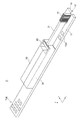
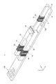
- FIG. 1 is a schematic perspective view showing the appearance of the magnetic sensor 1 according to the first embodiment of the present invention.
- FIG. 2 is a substantially exploded perspective view of the magnetic sensor 1.
- FIG. 3 is a schematic plan view of the sensor chip 20.
- FIG. 4 is a schematic cross-sectional view taken along the line AA of FIG.
- FIG. 5 is a schematic cross-sectional view for explaining an example in which the magnetic material layer and the magnetic sensitive element overlap.
- FIG. 6 is a circuit diagram for explaining the connection relationship between the magnetic sensing elements R1 to R4 and the compensation coil 41.
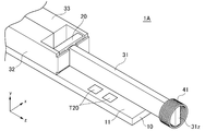
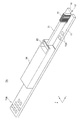
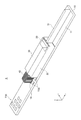
- FIG. 7 is a schematic perspective view showing the appearance of the magnetic sensor 1A according to the first modification of the first embodiment.
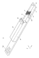
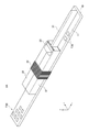
- FIG. 8 is a schematic perspective view showing the appearance of the magnetic sensor 1B according to the second modification of the first embodiment.
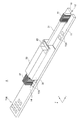
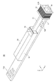
- FIG. 9 is a schematic perspective view showing the appearance of the magnetic sensor 2 according to the second embodiment of the present invention.
- FIG. 10 is a schematic perspective view showing the appearance of the magnetic sensor 2A according to the modified example of the second embodiment.
- FIG. 11 is a schematic perspective view showing the appearance of the magnetic sensor 3 according to the third embodiment of the present invention.
- FIG. 12 is a schematic perspective view showing the appearance of the magnetic sensor 4 according to the fourth embodiment of the present invention.
- FIG. 13 is a schematic perspective view showing the appearance of the magnetic sensor 4A according to the modified example of the fourth embodiment.
- FIG. 14 is a schematic perspective view showing the appearance of the magnetic sensor 5 according to the fifth embodiment of the present invention.
- FIG. 15 is a schematic perspective view showing the appearance of the magnetic sensor 6 according to the sixth embodiment of the present invention.
- FIG. 16 is a schematic perspective view showing the appearance of the magnetic sensor 6A according to the modified example of the sixth embodiment.
- FIG. 17 is a schematic perspective view showing the appearance of the magnetic sensor 7 according to the seventh embodiment of the present invention.
- FIG. 18 is a schematic perspective view showing the appearance of the magnetic sensor 8 according to the eighth embodiment of the present invention.
- FIG. 19 is a schematic perspective view showing the appearance of the magnetic sensor 8A according to the first modification of the eighth embodiment.
- FIG. 20 is a schematic perspective view showing the appearance of the magnetic sensor 8B according to the second modification of the eighth embodiment.
- FIG. 21 is a schematic perspective view showing the appearance of the magnetic sensor 9 according to the ninth embodiment of the present invention.
- FIG. 1 is a schematic perspective view showing the appearance of the magnetic sensor 1 according to the first embodiment of the present invention. Further, FIG. 2 is a substantially disassembled perspective view of the magnetic sensor 1.
- the magnetic sensor 1 includes a substrate 10, a sensor chip 20 mounted on a surface 11 forming the xz surface of the substrate 10, and external magnetic bodies 31 to 33.
- the compensating coil 41 wound around the external magnetic body 31 is provided.
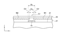
- the sensor chip 20 has an element forming surface 21 and a back surface 22 forming the xy surface, side surfaces 23 and 24 forming the yz surface, and side surfaces 25 and 26 forming the xz surface, and the side surface 26 is a substrate. It is mounted on the substrate 10 so as to face the surface 11 of the 10. Magnetic elements and magnetic material layers M1 to M3, which will be described later, are formed on the element forming surface 21 of the sensor chip 20.
- the surface 11 of the substrate 10 and the element forming surface 21 of the sensor chip 20 are perpendicular to each other.
- the external magnetic materials 31 to 33 play a role of collecting magnetic flux in the sensor chip 20, and all of them are made of a high magnetic permeability material such as ferrite.
- the external magnetic body 31 is a rod-shaped body whose longitudinal direction is the z direction, and is positioned at a substantially central portion of the element forming surface 21 in the x direction so as to cover a part of the magnetic body layer M1.
- the external magnetic material 32 covers a part of the magnetic material layer M2 and also covers the side surface 24 and the back surface 22 of the sensor chip 20, and has a rod-like shape with the z direction as the longitudinal direction.
- the external magnetic material 33 covers a part of the magnetic material layer M3 and also covers the side surface 23 and the back surface 22 of the sensor chip 20, and has a rod-like shape with the z direction as the longitudinal direction.
- the compensation coil 41 is composed of a wire (covered conducting wire) wound around an external magnetic body 31 so that the z direction is the axial direction. As shown in FIGS. 1 and 2, the external magnetic body 31 has a protruding portion 31z protruding from the substrate 10 in the z direction, and the compensation coil 41 is wound around the protruding portion 31z. In this embodiment, the compensation coil 41 is wound directly around the external magnetic body 31. Further, in order to prevent the winding from collapsing, the compensation coil 41 wound around the external magnetic body 31 may be hardened with an adhesive or the like.
- the number of turns of the wire constituting the compensation coil 41 is not particularly limited, and may be the number of turns required to generate the target cancel magnetic field.
- the compensation coil 41 is wound around the external magnetic body 31, the number of turns can be significantly increased as compared with the method in which the compensation coil is integrated on the sensor chip 20, and more. It is possible to pass a large current. Further, unlike the method in which the compensation coil is separately arranged on the substrate, the size of the entire magnetic sensor does not increase.
- FIG. 3 is a schematic plan view of the sensor chip 20
- FIG. 4 is a schematic cross-sectional view taken along the line AA of FIG.
- the magnetosensitizing elements R1 to R4 are not particularly limited as long as they are elements whose electrical resistance changes depending on the direction of magnetic flux, and for example, MR elements or the like can be used.
- the fixed magnetization directions of the magnetic sensing elements R1 to R4 are aligned with each other (for example, the plus side in the x direction).
- the magnetic sensitive elements R1 to R4 are covered with an insulating layer 27, and magnetic material layers M1 to M3 made of permalloy or the like are formed on the surface of the insulating layer 27.
- the magnetic material layers M1 to M3 are covered with an insulating layer 28.
- the portions of the magnetic layers M1 to M3 located on one side (upper side in FIG. 3) in the y direction are defined as magnetic layers M11, M21, and M31, and the other side in the y direction (lower side in FIG. 3).
- the magnetic sensitive element R1 is located between the magnetic material layer M11 and the magnetic material layer M21 in a plan view (when viewed from the z direction).
- the magnetic sensor R2 is located between the magnetic layer M12 and the magnetic layer M22
- the magnetic sensor R3 is located between the magnetic layer M11 and the magnetic layer M31
- the magnetic sensor R4 is located between the magnetic layer M12 and the magnetic layer M12. It is located between the magnetic layers M32.
- a magnetic field passing through the magnetic gaps G1 to G4 is applied to the magnetic sensing elements R1 to R4.
- the magnetic sensing elements R1 to R4 are located between the two magnetic material layers in a plan view, and the vicinity of the magnetic gaps G1 to G4 composed of the two magnetic material layers, that is, the magnetic gap. It suffices if the magnetic sensing elements R1 to R4 are arranged on the magnetic path formed by G1 to G4. Further, the width of the magnetic gaps G1 to G4 does not have to be wider than the width of the magnetic gaps R1 to R4, and the width of the magnetic gaps G1 to G4 may be narrower than the widths of the magnetic gaps R1 to R4. In the example shown in FIG.
- the width Gx of the magnetic gap G1 in the x direction is narrower than the width Rx of the magnetic sensor R1 in the x direction, whereby the magnetic material layers M1 and M2 and the magnetic sensor R1 are viewed from the z direction.
- the relationship between the magnetic gaps G1 to G4 and the magnetic sensing elements R1 to R4 may be the relationship shown in FIG.
- the regions indicated by reference numerals 31a to 33a indicate regions covered by the external magnetic materials 31 to 33, respectively.
- the external magnetic material 31 covers the magnetic material layer M1
- the external magnetic material 32 covers the magnetic material layer M2
- the external magnetic material 33 covers the magnetic material layer M3.
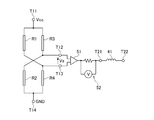
- FIG. 6 is a circuit diagram for explaining the connection relationship between the magnetic sensing elements R1 to R4 and the compensation coil 41.
- the magnetic sensor R1 is connected between the terminal electrodes T11 and T13
- the magnetic sensor R2 is connected between the terminal electrodes T12 and T14
- the magnetic sensor R3 is connected between the terminal electrodes T11 and T12.
- the magnetic sensing element R4 is connected between the terminal electrodes T13 and T14.
- the terminal electrodes T11 to T14 are terminal electrodes constituting the terminal electrode group T10 shown in FIG.
- the terminal electrode group T10 is provided on the sensor chip 20 and is connected to the terminal electrode group T30 shown in FIGS. 1 and 2 via a wiring (not shown) formed on the substrate 10.
- a power supply potential Vcc is given to the terminal electrode T11
- a ground potential GND is given to the terminal electrode T14.
- the magnetic sensing elements R1 to R4 Since all the magnetic sensing elements R1 to R4 have the same magnetization fixing direction, the resistance change amount of the magnetic sensing elements R1 and R2 located on one side of the external magnetic body 31 and the external magnetic body 31 There is a difference between the resistance changes of the magnetic sensing elements R3 and R4 located on the other side of the magnetism. As a result, the magnetic sensing elements R1 to R4 form a differential bridge circuit, and changes in the electrical resistance of the magnetic sensing elements R1 to R4 according to the magnetic flux density appear as differential signals Va on the terminal electrodes T12 and T13. ..
- the differential signal Va output from the terminal electrodes T12 and T13 is input to the differential amplifier 51 provided on the substrate 10 or the sensor chip 20.
- the output signal of the differential amplifier 51 is fed back to the terminal electrode T21.
- a compensation coil 41 is connected between the terminal electrode T21 and the terminal electrode T22, whereby the compensation coil 41 generates a canceling magnetic field corresponding to the output signal of the differential amplifier 51. ..
- the terminal electrodes T21 and T22 are terminal electrodes constituting the terminal electrode group T20 shown in FIGS. 1 and 2.
- the compensation coil 41 is wound around the external magnetic body 31, a sufficient number of turns can be secured and a larger current can be passed. As a result, a strong canceling magnetic field can be generated, so that even when the magnetic field to be measured is relatively strong, not only can the magnetic fields applied to the magnetic sensing elements R1 to R4 be correctly canceled, but also the magnetic fields applied to the magnetic sensing elements R1 to R4 can be correctly canceled. It is possible to prevent magnetic saturation of the external magnetic material 31.
- the external magnetic body 31 since the external magnetic body 31 has the protruding portion 31z and the compensating coil 41 is wound around the protruding portion 31z, contact or interference between the compensating coil 41 and the substrate 10 occurs. Does not occur. As a result, the external magnetic body 31 can be brought into close contact with the surface 11 of the substrate 10, so that the external magnetic body 31 can be stably fixed to the surface 11 of the substrate 10.
- FIG. 7 is a schematic perspective view showing the appearance of the magnetic sensor 1A according to the first modification of the present embodiment.
- the magnetic sensor 1A according to the first modification is different from the above-mentioned magnetic sensor 1 in that the compensation coil 41 is formed of a circular air-core coil.
- the compensation coil 41 is formed of a circular air-core coil.
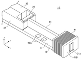
- FIG. 8 is a schematic perspective view showing the appearance of the magnetic sensor 1B according to the second modification of the present embodiment.
- the magnetic sensor 1B according to the second modification is different from the magnetic sensor 1 described above in that the compensation coil 41 is wound around the external magnetic body 31 via a bobbin 41B made of resin or the like. It's different. If the compensation coil 41 is wound around the bobbin 41B in this way, the work of directly winding the compensation coil 41 around the external magnetic body 31 becomes unnecessary, and the compensation coil 41 wound around the bobbin 41B is wound around the external magnetic body 31. It is enough to install it.
- FIG. 9 is a schematic perspective view showing the appearance of the magnetic sensor 2 according to the second embodiment of the present invention.
- the magnetic sensor 2 according to the second embodiment is different from the magnetic sensor 1 according to the first embodiment in that the substrate 10 is provided with the slit 12.
- the "slit” means a notch that is not closed, that is, the inner wall surface is continuously connected to the side surface of the substrate 10.
- the slit 12 overlaps with the external magnetic body 31 when viewed from the y direction, and the compensation coil 41 is wound around the portion of the external magnetic body 31 that overlaps with the slit 12. Since the other basic configurations are the same as those of the magnetic sensor 1 according to the first embodiment, the same elements are designated by the same reference numerals, and duplicate description will be omitted.
- the slit 12 is provided in the substrate 10, and the compensation coil 41 is wound around the portion overlapping the slit 12, so that the first embodiment is performed. Similar to the embodiment, the compensation coil 41 and the substrate 10 do not come into contact with each other. Moreover, since the external magnetic body 31 does not protrude from the substrate 10, the external magnetic body 31 is less likely to be damaged by an external force.
- FIG. 10 is a schematic perspective view showing the appearance of the magnetic sensor 2A according to a modified example of the present embodiment.
- the magnetic sensor 2A according to the modified example uses an external magnetic body 34 in which the external magnetic body 32 and the external magnetic body 33 are not separate parts but are integrated with each other.
- an integrated external magnetic material 34 may be used.
- FIG. 11 is a schematic perspective view showing the appearance of the magnetic sensor 3 according to the third embodiment of the present invention.
- the magnetic sensor 3 according to the third embodiment is different from the magnetic sensor 2 according to the second embodiment in that the substrate 10 is provided with the opening 13.
- opening is meant an independent notch that is closed, that is, the inner wall surface is not continuously connected to the side surface of the substrate 10.
- the opening 13 overlaps with the external magnetic body 31 when viewed from the y direction, and the compensation coil 41 is wound around the portion of the external magnetic body 31 that overlaps with the opening 13. Since the other basic configurations are the same as those of the magnetic sensor 2 according to the second embodiment, the same elements are designated by the same reference numerals, and duplicate description will be omitted.
- the substrate 10 is provided with the opening 13, and the compensation coil 41 is wound around the portion overlapping the opening 13. Similar to the above embodiment, the compensation coil 41 and the substrate 10 do not come into contact with each other. Moreover, since the external magnetic body 31 does not protrude from the substrate 10, the external magnetic body 31 is less likely to be damaged by an external force. Further, by changing the position of the opening 13 in the z direction, the compensation coil 41 can be wound at an arbitrary position in the z direction.
- FIG. 12 is a schematic perspective view showing the appearance of the magnetic sensor 4 according to the fourth embodiment of the present invention.
- the width of the end portion of the external magnetic bodies 32 and 33 in the z direction in the x direction is narrow, and another compensation coil 42 is wound around this portion. It differs from the magnetic sensor 2 according to the second embodiment in that it is rotated. Further, the substrate 10 is provided with an opening 14 as well as a slit 12. Since the other basic configurations are the same as those of the magnetic sensor 2 according to the second embodiment, the same elements are designated by the same reference numerals, and duplicate description will be omitted.
- the opening 14 overlaps with the external magnetic bodies 32 and 33 when viewed from the y direction, and the compensation coil 42 is wound around the portion of the external magnetic bodies 32 and 33 that overlaps with the opening 14.
- the coil axis of the compensation coil 42 is in the z direction, and is wound in the same direction as the compensation coil 41 wound around the external magnetic body 31.
- the compensation coil 41 and the compensation coil 42 are preferably connected in series. If the compensation coil 41 and the compensation coil 42 are connected in series, the same compensation current flows through the compensation coils 41 and 42. Therefore, the compensation coil 41 cancels the magnetic flux passing through the external magnetic body 31, and the compensation coil 42 cancels the magnetic flux. The magnetic flux passing through the external magnetic bodies 32 and 33 is canceled. Therefore, not only the external magnetic material 31 but also the magnetic saturation of the external magnetic materials 32 and 33 is prevented.
- FIG. 13 is a schematic perspective view showing the appearance of the magnetic sensor 4A according to a modified example of the present embodiment.
- the magnetic sensor 4A according to the modified example is provided with an opening 13 instead of the slit 12, and the compensation coil 41 is wound around the external magnetic body 31 at a position overlapping the opening 13.
- the lengths of the openings 13 and 14 in the z direction are also expanded, which increases the number of turns of the compensation coils 41 and 42. In this way, when it is necessary to increase the number of turns of the compensation coils 41 and 42, the lengths of the openings 13 and 14 in the z direction may be increased.
- FIG. 14 is a schematic perspective view showing the appearance of the magnetic sensor 5 according to the fifth embodiment of the present invention.
- the magnetic sensor 5 according to the fifth embodiment is provided with an opening 13 instead of the slit 12, and another slits 15 and 16 are provided on the substrate 10. Then, the compensation coil 43 is wound around the position of the external magnetic body 32 that overlaps with the slit 15, and the compensation coil 44 is wound around the position of the external magnetic body 33 that overlaps with the slit 16. Since the other basic configurations are the same as those of the magnetic sensor 4 according to the fourth embodiment, the same elements are designated by the same reference numerals, and duplicate description will be omitted.
- the compensation coil when the compensation coil is wound around the external magnetic bodies 32 and 33, it is not necessary to wind the compensation coil 42 together with the external magnetic bodies 32 and 33, and the external magnetic bodies 32 and 33 do not need to be wound together.
- the compensation coils 43 and 44 may be wound around the coil, respectively. According to this, the number of turns of the compensation coil can be finely adjusted.
- FIG. 15 is a schematic perspective view showing the appearance of the magnetic sensor 6 according to the sixth embodiment of the present invention.
- the magnetic sensor 6 according to the sixth embodiment is different from the magnetic sensor 4 according to the fourth embodiment in that the compensation coil 41 is omitted. Along with this, the slit 12 of the substrate 10 is also omitted. Since the other basic configurations are the same as those of the magnetic sensor 4 according to the fourth embodiment, the same elements are designated by the same reference numerals, and duplicate description will be omitted.
- the compensation coil 41 As illustrated in this embodiment, it is not essential to wind the compensation coil 41 around the external magnetic body 31, and instead of omitting the compensation coil 41, the compensation coil 42 is wound around the external magnetic bodies 32 and 33. It doesn't matter.
- FIG. 16 is a schematic perspective view showing the appearance of the magnetic sensor 6A according to a modified example of the present embodiment.
- the magnetic sensor 6A according to the modified example has a constricted shape in which the width of the external magnetic bodies 32 and 33 in the x direction becomes narrower in the middle of the longitudinal direction, and the compensating coil 42 is formed in the constricted portion. Is wound around. According to this, the compensation coil 42 is less likely to fall off.
- FIG. 17 is a schematic perspective view showing the appearance of the magnetic sensor 7 according to the seventh embodiment of the present invention.
- the magnetic sensor 7 according to the seventh embodiment is based on the first embodiment in that the tip of the external magnetic body 31 is thin and the external magnetic body 31 does not protrude from the substrate 10. It is different from the magnetic sensor 1. Since the other basic configurations are the same as those of the magnetic sensor 1 according to the first embodiment, the same elements are designated by the same reference numerals, and duplicate description will be omitted.
- the tip of the external magnetic body 31 is tapered in the x-direction and the y-direction. This narrowed portion constitutes a separation portion 31s away from the surface 11 of the substrate 10. Then, in the present embodiment, the compensation coil 41 is wound around the separation portion 31s to prevent the compensation coil 41 from coming into contact with the substrate 10.
- the compensation coil 41 may be wound at a position where it overlaps with the substrate 10.
- the separation portion 31s is tapered in the x-direction and the y-direction, but the separation portion 31s for preventing contact between the compensation coil 41 and the substrate 10 may have any shape. ..
- FIG. 18 is a schematic perspective view showing the appearance of the magnetic sensor 8 according to the eighth embodiment of the present invention.
- the width of the end portion 10a of the substrate 10 overlapping the tip of the external magnetic body 31 is as narrow as that of the external magnetic body 31, and the compensation coil 41 Is wound around both the end portion 10a of the substrate 10 and the external magnetic body 31, which is different from the magnetic sensor 1 according to the first embodiment.
- the external magnetic body 31 does not have the protruding portion 31z, and the whole overlaps with the substrate 10. Since the other basic configurations are the same as those of the magnetic sensor 1 according to the first embodiment, the same elements are designated by the same reference numerals, and duplicate description will be omitted.
- the compensation coil 41 may be wound around both the external magnetic material 31 and the substrate 10. Even in this case, interference between the compensation coil 41 and the substrate 10 can be prevented, and since the entire external magnetic body 31 overlaps with the substrate 10, damage to the external magnetic body 31 due to an external force is less likely to occur.
- FIG. 19 is a schematic perspective view showing the appearance of the magnetic sensor 8A according to the first modification of the present embodiment.
- the compensation coil 42 is wound around both the external magnetic bodies 32 and 33 and the substrate 10 instead of omitting the compensation coil 41.
- the compensating coil 42 wound around the external magnetic bodies 32 and 33 may be wound together with the substrate 10.
- FIG. 20 is a schematic perspective view showing the appearance of the magnetic sensor 8B according to the second modification of the present embodiment.
- the compensation coil 41 is wound around the bobbin 41B made of resin or the like, and the substrate 10 and the external magnetic body 31 are inserted into the inner diameter region of the bobbin 41B. There is. If the compensating coil 41 is wound around the bobbin 41B in this way, the work of directly winding the compensating coil 41 around the external magnetic body 31 becomes unnecessary. That is, since the sensor chip 20 and the external magnetic body 31 are mounted on the substrate 10 and then the bobbin 41B around which the compensation coil 41 is wound is inserted into the substrate 10, the workability of the assembly work is improved. Moreover, since the bobbin 41B is used, the compensation coil 41 can be wound accurately, and as a result, the accuracy of the applied magnetic field by the compensation coil 41 is improved.
- FIG. 21 is a schematic perspective view showing the appearance of the magnetic sensor 9 according to the ninth embodiment of the present invention.
- the magnetic sensor 9 according to the ninth embodiment is different from the magnetic sensor 1 according to the first embodiment in that the external magnetic body 31 does not protrude from the substrate 10. Along with this, the external magnetic body 31 does not have the protruding portion 31z, and the whole overlaps with the substrate 10. Since the other basic configurations are the same as those of the magnetic sensor 1 according to the first embodiment, the same elements are designated by the same reference numerals, and duplicate description will be omitted.
- the four magnetic sensing elements R1 to R4 are bridge-connected, but it is not essential to use the four magnetic sensing elements in the present invention.
Landscapes
- Physics & Mathematics (AREA)
- Condensed Matter Physics & Semiconductors (AREA)
- General Physics & Mathematics (AREA)
- Measuring Magnetic Variables (AREA)
Abstract
【課題】クローズドループ制御が可能な小型の磁気センサを提供する。 【解決手段】磁気センサ1は、素子形成面が基板10の表面11に対して垂直又は所定の傾きを持つよう、基板10の表面11に搭載されたセンサチップ20と、基板10の表面11に搭載され、検出対象磁界を感磁素子に集磁する外部磁性体31と、外部磁性体31に巻回された補償コイル41とを備える。このように、補償コイル41が外部磁性体31に巻回されていることから、感磁素子に印加される磁界をキャンセルすることができるとともに、外部磁性体31の磁気飽和を防止することができる。
Description
本発明は磁気センサに関し、特に、感磁素子に磁束を集める外部磁性体と補償コイルを備えた磁気センサに関する。
感磁素子に磁束を集める外部磁性体と補償コイルを備えた磁気センサとしては、特許文献1及び2に記載された磁気センサが知られている。特許文献1及び2に記載された磁気センサは、センサチップに集積された感磁素子及び補償コイルと、センサチップ上に配置された外部磁性体とを備えている。そして、外部磁性体によって集磁された磁界が感磁素子に印加されるとともに、感磁素子に印加される磁界を補償コイルによってキャンセルすることによって、いわゆるクローズドループ制御が行われる。これにより、感磁素子に印加される磁界が常にゼロの状態が保たれることから、温度変化などに起因するオフセットが生じず、正確な磁界測定が可能となる。
しかしながら、特許文献1及び2に記載された磁気センサでは、補償コイルがセンサチップに集積された構造を有していることから、補償コイルのターン数を十分に確保することが困難であり、このため補償コイルに流れる電流から発生する磁界が比較的小さい。このため、測定対象となる磁界が比較的強い場合には、感磁素子に印加される磁界をキャンセルすることが困難であった。また、補償コイルと外部磁性体の距離が離れていることから、測定対象となる磁界が強いと外部磁性体が磁気飽和してしまうことも考えられる。外部磁性体が磁気飽和すると、集磁能力の低下によって、磁界の強度とセンサ出力との間のリニアリティがなくなり、正確な磁界測定ができなくなるという問題があった。
このような問題を解決する方法としては、特許文献1の図12に示すように、センサチップが搭載された基板上に、センサチップを取り囲むような大型の補償コイルを別途付加する方法が考えられる。この方法によれば、感磁素子及び外部磁性体に強いキャンセル磁界を印加することができるため、測定対象となる磁界が比較的強い場合であっても、感磁素子に印加される磁界を正しくキャンセルすることができるとともに、外部磁性体の磁気飽和を防止することが可能となる。
しかしながら、大型の補償コイルを基板上に搭載する方法では、磁気センサ全体のサイズが大型化するという問題があった。
したがって、本発明は、感磁素子に印加される磁界を補償コイルによって正しくキャンセルすることができ、且つ、外部磁性体の磁気飽和を防止することが可能な小型の磁気センサを提供することを目的とする。
本発明による磁気センサは、基板と、少なくとも一つの感磁素子が形成された素子形成面が基板の表面に対して垂直又は所定の傾きを持つよう、基板の表面に搭載されたセンサチップと、基板の表面に搭載され、検出対象磁界を感磁素子に集磁する少なくとも一つの外部磁性体と、外部磁性体に巻回された補償コイルとを備えることを特徴とする。
本発明によれば、補償コイルが外部磁性体に巻回されていることから、コイル径を小さくできる。このため、磁気センサ全体のサイズの大型化を防止しつつ、キャンセル磁界を外部磁性体に効率よく印加することが可能となる。これにより、感磁素子に印加される磁界を正しくキャンセルすることができるとともに、外部磁性体の磁気飽和を防止することが可能となる。しかも、外部磁性体が基板の表面に搭載されていることから、外部磁性体の長さが長い場合であっても、基板上に外部磁性体を安定して支持することが可能となる。また、補償コイルを別部品として配置しなくても良いので、補償コイルの位置ずれ等によるキャンセル磁界の変化が低減され、安定した歩留まりでセンサを提供できる。
本発明において、補償コイルは、基板と重ならない位置において外部磁性体に巻回されていても構わない。これによれば、補償コイルと基板の接触によって外部磁性体の支持が不安定となることもない。この場合、外部磁性体は基板の表面から突出した突出部を有しており、補償コイルは突出部に巻回されていても構わない。或いは、基板が外部磁性体と重なるスリット又は開口部を有しており、補償コイルはスリット又は開口部と重なる位置に設けられていても構わない。これらによれば、補償コイルと基板の接触を防止することが可能となる。
本発明において、外部磁性体は基板の表面から離れた離間部を有しており、補償コイルは外部磁性体の離間部に巻回されていても構わない。これによれば、補償コイルを基板と重なる位置に配置しつつ、基板との接触を防止することが可能となる。
本発明において、補償コイルは外部磁性体と基板の両方に巻回されていても構わない。これによれば、補償コイルと基板の干渉を防止しつつ、外力による外部磁性体の破損を防止することが可能となる。
本発明において、少なくとも一つの感磁素子は、第1及び第2の感磁素子を含むブリッジ接続された複数の感磁素子からなり、少なくとも一つの外部磁性体は、素子形成面に対して垂直な方向から見て、第1の感磁素子と第2の感磁素子の間に配置された第1の外部磁性体を含むものであっても構わない。これによれば、第1及び第2の感磁素子に対して逆方向の磁界を与えることが可能となる。この場合、補償コイルは、第1の外部磁性体に巻回されていても構わない。これによれば、キャンセル磁界を第1の外部磁性体に効率よく印加することが可能となる。
本発明において、少なくとも一つの外部磁性体は、素子形成面の反対側に位置するセンサチップの裏面を覆う第2の外部磁性体をさらに含むものであっても構わない。これによれば、感磁素子に印加される磁界の強度がより高められる。この場合、補償コイルは、第2の外部磁性体に巻回されていても構わない。これによれば、キャンセル磁界を第2の外部磁性体に効率よく印加することが可能となる。
本発明において、補償コイルはボビンを介して外部磁性体に巻回されていても構わない。これによれば、外部磁性体に補償コイルを直接巻回する作業が不要となる。この場合、ボビンの内径領域には基板及び外部磁性体が挿入されていても構わない。これによれば、基板にセンサチップ及び外部磁性体を実装した後、補償コイルが巻かれたボビンを基板に挿入することによって作製できることから、アセンブリ作業の作業性が向上する。
このように、本発明による磁気センサは、感磁素子に印加される磁界を補償コイルによって正しくキャンセルすることができ、且つ、外部磁性体の磁気飽和を防止することができる。しかも、補償コイルが外部磁性体に巻回されていることから、磁気センサ全体のサイズの大型化も防止される。さらに、基板と接触することなく補償コイルが巻回されていることから、補償コイルと基板の接触によって外部磁性体の支持が不安定となることもない。
以下、添付図面を参照しながら、本発明の好ましい実施形態について詳細に説明する。
図1は、本発明の第1の実施形態による磁気センサ1の外観を示す略斜視図である。また、図2は、磁気センサ1の略分解斜視図である。
図1及び図2に示すように、第1の実施形態による磁気センサ1は、基板10と、基板10のxz面を構成する表面11に搭載されたセンサチップ20及び外部磁性体31~33と、外部磁性体31に巻回された補償コイル41とを備えている。センサチップ20は、xy面を構成する素子形成面21及び裏面22と、yz面を構成する側面23,24と、xz面を構成する側面25,26とを有しており、側面26が基板10の表面11と向かい合うよう、基板10に搭載されている。センサチップ20の素子形成面21上には、後述する感磁素子及び磁性体層M1~M3が形成されている。このように、本実施形態においては、基板10の表面11とセンサチップ20の素子形成面21が垂直である。但し、本発明おいて両者が完全に垂直であることは必須でなく、垂直に対して所定の傾きを有していても構わない。
外部磁性体31~33は、センサチップ20に磁束を集める役割を果たし、いずれもフェライトなどの高透磁率材料によって構成される。このうち、外部磁性体31はz方向を長手方向とする棒状体であり、磁性体層M1の一部を覆うよう、素子形成面21のx方向における略中央部に位置決めされている。外部磁性体32は、磁性体層M2の一部を覆うとともに、センサチップ20の側面24及び裏面22を覆っており、z方向を長手方向とする棒状形状を有している。同様に、外部磁性体33は、磁性体層M3の一部を覆うとともに、センサチップ20の側面23及び裏面22を覆っており、z方向を長手方向とする棒状形状を有している。かかる構成により、z方向の磁界が選択的に集磁され、集磁された磁界がセンサチップ20に印加されることになる。
補償コイル41は、z方向が軸方向となるよう外部磁性体31に巻回されたワイヤ(被覆導線)からなる。図1及び図2に示すように、外部磁性体31は、基板10からz方向に突出した突出部31zを有しており、補償コイル41がこの突出部31zに巻回されている。本実施形態においては、補償コイル41が外部磁性体31に直接巻回されている。また、巻崩れを防止するために、外部磁性体31に巻回した補償コイル41を接着剤などで固めても構わない。補償コイル41を構成するワイヤのターン数については特に限定されず、目的とするキャンセル磁界の発生に必要なターン数とすれば良い。本実施形態においては、補償コイル41を外部磁性体31に巻回していることから、センサチップ20に補償コイルを集積する方式と比べて、ターン数を大幅に増やすことが可能であるとともに、より大きな電流を流すことが可能である。また、基板上に補償コイルを別途配置する方式のように、磁気センサ全体のサイズが大型化することもない。
図3はセンサチップ20の略平面図であり、図4は図3のA-A線に沿った略断面図である。
図3及び図4に示すように、センサチップ20の素子形成面21には、4つの感磁素子R1~R4が形成されている。感磁素子R1~R4は、磁束の向きによって電気抵抗が変化する素子であれば特に限定されず、例えばMR素子などを用いることができる。感磁素子R1~R4の固定磁化方向は、互いに同じ向き(例えばx方向におけるプラス側)に揃えられている。感磁素子R1~R4は絶縁層27で覆われており、絶縁層27の表面には、パーマロイなどからなる磁性体層M1~M3が形成されている。磁性体層M1~M3は絶縁層28で覆われている。そして、磁性体層M1~M3のうち、y方向における一方側(図3における上側)に位置する部分を磁性体層M11,M21,M31と定義し、y方向における他方側(図3における下側)に位置する部分を磁性体層M12,M22,M32と定義した場合、平面視で(z方向から見て)、感磁素子R1は磁性体層M11と磁性体層M21の間に位置し、感磁素子R2は磁性体層M12と磁性体層M22の間に位置し、感磁素子R3は磁性体層M11と磁性体層M31の間に位置し、感磁素子R4は磁性体層M12と磁性体層M32の間に位置している。これにより、磁気ギャップG1~G4を通過する磁界が感磁素子R1~R4に印加される。
但し、本発明において、各感磁素子R1~R4が平面視で2つの磁性体層間に位置することは必須でなく、2つの磁性体層からなる磁気ギャップG1~G4の近傍、つまり、磁気ギャップG1~G4によって形成される磁路上に各感磁素子R1~R4が配置されていれば足りる。また、磁気ギャップG1~G4の幅が感磁素子R1~R4の幅よりも広い必要はなく、磁気ギャップG1~G4の幅が感磁素子R1~R4よりも狭くても構わない。図5に示す例では、磁気ギャップG1のx方向における幅Gxが感磁素子R1のx方向における幅Rxよりも狭く、これにより、z方向から見て磁性体層M1,M2と感磁素子R1が重なりOVを有している。磁気ギャップG1~G4と感磁素子R1~R4との関係は、図5に示す関係であっても構わない。
図3及び図4において、符号31a~33aで示す領域はそれぞれ外部磁性体31~33によって覆われる領域を示している。図3及び図4に示すように、外部磁性体31は磁性体層M1を覆い、外部磁性体32は磁性体層M2を覆い、外部磁性体33は磁性体層M3を覆う。
図6は、感磁素子R1~R4と補償コイル41の接続関係を説明するための回路図である。
図6に示すように、感磁素子R1は端子電極T11,T13間に接続され、感磁素子R2は端子電極T12,T14間に接続され、感磁素子R3は端子電極T11,T12間に接続され、感磁素子R4は端子電極T13,T14間に接続されている。端子電極T11~T14は、図2に示す端子電極群T10を構成する端子電極である。端子電極群T10はセンサチップ20に設けられ、基板10に形成された図示しない配線を介して、図1及び図2に示す端子電極群T30に接続される。端子電極T11には電源電位Vccが与えられ、端子電極T14には接地電位GNDが与えられる。そして、感磁素子R1~R4は全て同一の磁化固定方向を有していることから、外部磁性体31からみて一方側に位置する感磁素子R1,R2の抵抗変化量と、外部磁性体31からみて他方側に位置する感磁素子R3,R4の抵抗変化量との間には差が生じる。これにより、感磁素子R1~R4は差動ブリッジ回路を構成し、磁束密度に応じた感磁素子R1~R4の電気抵抗の変化が差動信号Vaとして端子電極T12,T13に現れることになる。
端子電極T12,T13から出力される差動信号Vaは、基板10又はセンサチップ20に設けられた差動アンプ51に入力される。差動アンプ51の出力信号は、端子電極T21にフィードバックされる。図6に示すように、端子電極T21と端子電極T22との間には補償コイル41が接続されており、これにより、補償コイル41は差動アンプ51の出力信号に応じたキャンセル磁界を発生させる。端子電極T21,T22は、図1及び図2に示す端子電極群T20を構成する端子電極である。かかる構成により、検出対象磁界の磁束密度に応じた感磁素子R1~R4の電気抵抗の変化に応じた差動信号Vaが端子電極T12,T13に現れると、これに応じた電流が補償コイル41に流れ、逆方向のキャンセル磁界を発生させる。これにより、検出対象磁界が打ち消される。そして、差動アンプ51から出力される電流を検出回路52によって電流電圧変換すれば、検出対象磁界の強さを検出することが可能となる。このようなクローズドループ制御により、外部磁性体31~33を介して集磁された磁界を高精度に検出することが可能となる。
そして、本実施形態においては、補償コイル41が外部磁性体31に巻回されていることから、十分なターン数を確保することができるとともに、より大きな電流を流すことが可能である。これにより、強いキャンセル磁界を発生させることができるため、測定対象となる磁界が比較的強い場合であっても、感磁素子R1~R4に印加される磁界を正しくキャンセルすることができるだけでなく、外部磁性体31の磁気飽和を防止することが可能となる。
しかも、本実施形態においては、外部磁性体31が突出部31zを有しており、補償コイル41がこの突出部31zに巻回されていることから、補償コイル41と基板10の接触や干渉が生じない。これにより、外部磁性体31を基板10の表面11に密着させることができることから、外部磁性体31を基板10の表面11に安定的に固定することが可能となる。
図7は、本実施形態の第1の変形例による磁気センサ1Aの外観を示す略斜視図である。図7に示すように、第1の変形例による磁気センサ1Aは、補償コイル41が円形の空芯コイルからなる点において、上述した磁気センサ1と相違する。このように、補償コイル41として空芯コイルを用いれば、外部磁性体31に補償コイル41を直接巻回する作業が不要となり、すでに巻回された補償コイル41を外部磁性体31に装着すれば足りる。
図8は、本実施形態の第2の変形例による磁気センサ1Bの外観を示す略斜視図である。図8に示すように、第2の変形例による磁気センサ1Bは、補償コイル41が樹脂などからなるボビン41Bを介して外部磁性体31に巻回されている点において、上述した磁気センサ1と相違する。このように、補償コイル41をボビン41Bに巻回すれば、外部磁性体31に補償コイル41を直接巻回する作業が不要となり、ボビン41Bに巻回された補償コイル41を外部磁性体31に装着すれば足りる。
図9は、本発明の第2の実施形態による磁気センサ2の外観を示す略斜視図である。
図9に示すように、第2の実施形態による磁気センサ2は、基板10にスリット12が設けられている点において、第1の実施形態による磁気センサ1と相違している。「スリット」とは閉じていない、つまり、内壁面が基板10の側面と連続的につながる切り欠きを意味する。スリット12はy方向から見て外部磁性体31と重なっており、外部磁性体31のうちスリット12と重なる部分に補償コイル41が巻回されている。その他の基本的な構成は、第1の実施形態による磁気センサ1と同一であることから、同一の要素には同一の符号を付し、重複する説明は省略する。
本実施形態においては、外部磁性体31が基板10から突出していないものの、基板10にスリット12が設けられ、スリット12と重なる部分に補償コイル41が巻回されていることから、第1の実施形態と同様、補償コイル41と基板10の接触が生じない。しかも、外部磁性体31が基板10から突出しないことから、外力による外部磁性体31の破損も生じにくくなる。
図10は、本実施形態の変形例による磁気センサ2Aの外観を示す略斜視図である。図10に示すように、変形例による磁気センサ2Aは、外部磁性体32と外部磁性体33が別部品ではなく、これらが一体化された外部磁性体34を用いている。本実施形態が例示するように、一体化された外部磁性体34を用いても構わない。
図11は、本発明の第3の実施形態による磁気センサ3の外観を示す略斜視図である。
図11に示すように、第3の実施形態による磁気センサ3は、基板10に開口部13が設けられている点において、第2の実施形態による磁気センサ2と相違している。「開口部」とは閉じた、つまり、内壁面が基板10の側面と連続的につながらない独立した切り欠きを意味する。開口部13はy方向から見て外部磁性体31と重なっており、外部磁性体31のうち開口部13と重なる部分に補償コイル41が巻回されている。その他の基本的な構成は、第2の実施形態による磁気センサ2と同一であることから、同一の要素には同一の符号を付し、重複する説明は省略する。
本実施形態においては、外部磁性体31が基板10から突出していないものの、基板10に開口部13が設けられ、開口部13と重なる部分に補償コイル41が巻回されていることから、第1の実施形態と同様、補償コイル41と基板10の接触が生じない。しかも、外部磁性体31が基板10から突出しないことから、外力による外部磁性体31の破損も生じにくくなる。さらに、開口部13のz方向位置を変更することにより、補償コイル41を任意のz方向位置に巻回することが可能となる。
図12は、本発明の第4の実施形態による磁気センサ4の外観を示す略斜視図である。
図12に示すように、第4の実施形態による磁気センサ4は、外部磁性体32,33のz方向における端部のx方向幅が狭くなっており、この部分に別の補償コイル42が巻回されている点において、第2の実施形態による磁気センサ2と相違している。さらに、基板10には、スリット12だけでなく開口部14が設けられている。その他の基本的な構成は、第2の実施形態による磁気センサ2と同一であることから、同一の要素には同一の符号を付し、重複する説明は省略する。
開口部14はy方向から見て外部磁性体32,33と重なっており、外部磁性体32,33のうち開口部14と重なる部分に補償コイル42が巻回されている。補償コイル42のコイル軸はz方向であり、外部磁性体31に巻回された補償コイル41と同方向に巻回される。補償コイル41と補償コイル42は、直列に接続することが好ましい。補償コイル41と補償コイル42を直列に接続すれば、補償コイル41,42に同じ補償電流が流れることから、補償コイル41によって外部磁性体31を通過する磁束がキャンセルされるとともに、補償コイル42によって外部磁性体32,33を通過する磁束がキャンセルされる。このため、外部磁性体31だけでなく、外部磁性体32,33の磁気飽和も防止される。
図13は、本実施形態の変形例による磁気センサ4Aの外観を示す略斜視図である。図13に示すように、変形例による磁気センサ4Aは、スリット12の代わりに開口部13が設けられており、外部磁性体31のうち開口部13と重なる位置に補償コイル41が巻回されている。また、開口部13,14のz方向における長さも拡大されており、これにより補償コイル41,42のターン数が増加している。このように、補償コイル41,42のターン数を増やす必要がある場合には、開口部13,14のz方向における長さを拡大すればよい。
図14は、本発明の第5の実施形態による磁気センサ5の外観を示す略斜視図である。
図14に示すように、第5の実施形態による磁気センサ5は、スリット12の代わりに開口部13が設けられ、且つ、基板10に別のスリット15,16が設けられている。そして、外部磁性体32のうちスリット15と重なる位置に補償コイル43が巻回され、外部磁性体33のうちスリット16と重なる位置に補償コイル44が巻回されている。その他の基本的な構成は、第4の実施形態による磁気センサ4と同一であることから、同一の要素には同一の符号を付し、重複する説明は省略する。
本実施形態が例示するように、外部磁性体32,33に補償コイルを巻回する場合、補償コイル42を外部磁性体32,33にまとめて巻回する必要はなく、外部磁性体32,33に補償コイル43,44をそれぞれ巻回しても構わない。これによれば、補償コイルのターン数をより細かく調整することが可能となる。
図15は、本発明の第6の実施形態による磁気センサ6の外観を示す略斜視図である。
図15に示すように、第6の実施形態による磁気センサ6は、補償コイル41が省略されている点において、第4の実施形態による磁気センサ4と相違している。これに伴い、基板10のスリット12も省略されている。その他の基本的な構成は、第4の実施形態による磁気センサ4と同一であることから、同一の要素には同一の符号を付し、重複する説明は省略する。
本実施形態が例示するように、外部磁性体31に補償コイル41を巻回することは必須でなく、補償コイル41を省略する代わりに、外部磁性体32,33に補償コイル42を巻回しても構わない。
図16は、本実施形態の変形例による磁気センサ6Aの外観を示す略斜視図である。図16に示すように、変形例による磁気センサ6Aは、外部磁性体32,33のx方向における幅が長手方向の途中で狭くなるくびれた形状を有しており、このくびれ部分に補償コイル42が巻回されている。これによれば、補償コイル42が脱落しにくくなる。
図17は、本発明の第7の実施形態による磁気センサ7の外観を示す略斜視図である。
図17に示すように、第7の実施形態による磁気センサ7は、外部磁性体31の先端が細くなっているとともに、外部磁性体31が基板10から突出しない点において、第1の実施形態による磁気センサ1と相違している。その他の基本的な構成は、第1の実施形態による磁気センサ1と同一であることから、同一の要素には同一の符号を付し、重複する説明は省略する。
図17に示す例では、外部磁性体31の先端がx方向及びy方向に細くなっている。この細くなった部分は、基板10の表面11から離れた離間部31sを構成する。そして、本実施形態においては、この離間部31sに補償コイル41を巻回することにより、補償コイル41と基板10の接触が防止されている。
本実施形態が例示するように、基板10と重なる位置に補償コイル41を巻回しても構わない。尚、図17に示す例では、離間部31sがx方向及びy方向に細くなっているが、補償コイル41と基板10の接触を防止する離間部31sがどのような形状であっても構わない。
図18は、本発明の第8の実施形態による磁気センサ8の外観を示す略斜視図である。
図18に示すように、第8の実施形態による磁気センサ8は、外部磁性体31の先端と重なる基板10の端部10aの幅が外部磁性体31と同程度に細く、且つ、補償コイル41が基板10の端部10aと外部磁性体31の両方に巻回されている点において、第1の実施形態による磁気センサ1と相違している。これに伴い、外部磁性体31は突出部31zを有しておらず、全体が基板10と重なっている。その他の基本的な構成は、第1の実施形態による磁気センサ1と同一であることから、同一の要素には同一の符号を付し、重複する説明は省略する。
本実施形態が例示するように、補償コイル41を外部磁性体31と基板10の両方に巻回しても構わない。この場合であっても、補償コイル41と基板10の干渉を防止することができるとともに、外部磁性体31の全体が基板10と重なることから、外力による外部磁性体31の破損も生じにくくなる。
図19は、本実施形態の第1の変形例による磁気センサ8Aの外観を示す略斜視図である。図19に示すように、変形例による磁気センサ8Aは、補償コイル41が省略される代わりに、外部磁性体32,33と基板10の両方に補償コイル42が巻回されている。このように、外部磁性体32,33に巻回する補償コイル42を基板10ごと巻回しても構わない。
図20は、本実施形態の第2の変形例による磁気センサ8Bの外観を示す略斜視図である。図20に示すように、変形例による磁気センサ8Bは、補償コイル41が樹脂などからなるボビン41Bに巻回されているとともに、ボビン41Bの内径領域に基板10及び外部磁性体31が挿入されている。このように、補償コイル41をボビン41Bに巻回すれば、外部磁性体31に補償コイル41を直接巻回する作業が不要となる。つまり、基板10にセンサチップ20及び外部磁性体31を実装した後、補償コイル41が巻かれたボビン41Bを基板10に挿入することによって作製できることから、アセンブリ作業の作業性が向上する。しかも、ボビン41Bを使用していることから、補償コイル41を正確に巻くことができ、その結果、補償コイル41による印加磁場精度が向上する。
図21は、本発明の第9の実施形態による磁気センサ9の外観を示す略斜視図である。
図21に示すように、第9の実施形態による磁気センサ9は、外部磁性体31が基板10から突出していない点において、第1の実施形態による磁気センサ1と相違している。これに伴い、外部磁性体31は突出部31zを有しておらず、全体が基板10と重なっている。その他の基本的な構成は、第1の実施形態による磁気センサ1と同一であることから、同一の要素には同一の符号を付し、重複する説明は省略する。
本実施形態が例示するように、本発明において補償コイル41と基板10の干渉を防止することは必須でない。
以上、本発明の好ましい実施形態について説明したが、本発明は、上記の実施形態に限定されることなく、本発明の主旨を逸脱しない範囲で種々の変更が可能であり、それらも本発明の範囲内に包含されるものであることはいうまでもない。
例えば、上記の各実施形態では、4つの感磁素子R1~R4をブリッジ接続しているが、本発明において4つの感磁素子を用いることは必須でない。
1,1A,1B,2,2A,3,4,4A,5,6,6A,7,8,8A,8B,9 磁気センサ
10 基板
10a 基板の端部
11 基板の表面
12,15,16 スリット
13,14 開口部
20 センサチップ
21 素子形成面
22 センサチップの裏面
23~26 センサチップの側面
27,28 絶縁層
31~33 外部磁性体
31s 離間部
31z 突出部
41~44 補償コイル
41B ボビン
51 差動アンプ
52 検出回路
G1~G4 磁気ギャップ
M1~M3,M11,M21,M31,M12,M22,M32 磁性体層
R1~R4 感磁素子
T10,T20,T30 端子電極群
T11~T14,T21,T22 端子電極
10 基板
10a 基板の端部
11 基板の表面
12,15,16 スリット
13,14 開口部
20 センサチップ
21 素子形成面
22 センサチップの裏面
23~26 センサチップの側面
27,28 絶縁層
31~33 外部磁性体
31s 離間部
31z 突出部
41~44 補償コイル
41B ボビン
51 差動アンプ
52 検出回路
G1~G4 磁気ギャップ
M1~M3,M11,M21,M31,M12,M22,M32 磁性体層
R1~R4 感磁素子
T10,T20,T30 端子電極群
T11~T14,T21,T22 端子電極
Claims (12)
- 基板と、
少なくとも一つの感磁素子が形成された素子形成面が前記基板の表面に対して垂直又は所定の傾きを持つよう、前記基板の表面に搭載されたセンサチップと、
前記基板の表面に搭載され、検出対象磁界を前記感磁素子に集磁する少なくとも一つの外部磁性体と、
前記外部磁性体に巻回された補償コイルと、を備えることを特徴とする磁気センサ。 - 前記補償コイルは、前記基板と重ならない位置において、前記外部磁性体に巻回されていることを特徴とする請求項1に記載の磁気センサ。
- 前記外部磁性体は、前記基板の表面から突出した突出部を有しており、
前記補償コイルは、前記突出部に巻回されていることを特徴とする請求項2に記載の磁気センサ。 - 前記基板は、前記外部磁性体と重なるスリット又は開口部を有しており、
前記補償コイルは、前記スリット又は前記開口部と重なる位置に設けられていることを特徴とする請求項2に記載の磁気センサ。 - 前記外部磁性体は、前記基板の表面から離れた離間部を有しており、
前記補償コイルは、前記外部磁性体の前記離間部に巻回されていることを特徴とする請求項1に記載の磁気センサ。 - 前記補償コイルは、前記外部磁性体と前記基板の両方に巻回されていることを特徴とする請求項1に記載の磁気センサ。
- 前記少なくとも一つの感磁素子は、第1及び第2の感磁素子を含むブリッジ接続された複数の感磁素子からなり、
前記少なくとも一つの外部磁性体は、前記素子形成面に対して垂直な方向から見て、前記第1の感磁素子と前記第2の感磁素子の間に配置された第1の外部磁性体を含むことを特徴とする請求項1乃至6のいずれか一項に記載の磁気センサ。 - 前記補償コイルは、前記第1の外部磁性体に巻回されていることを特徴とする請求項7に記載の磁気センサ。
- 前記少なくとも一つの外部磁性体は、前記素子形成面の反対側に位置する前記センサチップの裏面を覆う第2の外部磁性体をさらに含むことを特徴とする請求項7又は8に記載の磁気センサ。
- 前記補償コイルは、前記第2の外部磁性体に巻回されていることを特徴とする請求項9に記載の磁気センサ。
- 前記補償コイルは、ボビンを介して前記外部磁性体に巻回されていることを特徴とする請求項1に記載の磁気センサ。
- 前記ボビンの内径領域には、前記基板及び前記外部磁性体が挿入されていることを特徴とする請求項11に記載の磁気センサ。
Priority Applications (4)
| Application Number | Priority Date | Filing Date | Title |
|---|---|---|---|
| EP20889844.5A EP4064374A4 (en) | 2019-11-22 | 2020-07-30 | MAGNETIC SENSOR |
| CN202080080483.4A CN114730831A (zh) | 2019-11-22 | 2020-07-30 | 磁传感器 |
| US17/778,249 US20220349960A1 (en) | 2019-11-22 | 2020-07-30 | Magnetic sensor |
| JP2021558170A JPWO2021100252A1 (ja) | 2019-11-22 | 2020-07-30 |
Applications Claiming Priority (2)
| Application Number | Priority Date | Filing Date | Title |
|---|---|---|---|
| JP2019211066 | 2019-11-22 | ||
| JP2019-211066 | 2019-11-22 |
Publications (1)
| Publication Number | Publication Date |
|---|---|
| WO2021100252A1 true WO2021100252A1 (ja) | 2021-05-27 |
Family
ID=75980485
Family Applications (1)
| Application Number | Title | Priority Date | Filing Date |
|---|---|---|---|
| PCT/JP2020/029194 WO2021100252A1 (ja) | 2019-11-22 | 2020-07-30 | 磁気センサ |
Country Status (5)
| Country | Link |
|---|---|
| US (1) | US20220349960A1 (ja) |
| EP (1) | EP4064374A4 (ja) |
| JP (1) | JPWO2021100252A1 (ja) |
| CN (1) | CN114730831A (ja) |
| WO (1) | WO2021100252A1 (ja) |
Cited By (4)
| Publication number | Priority date | Publication date | Assignee | Title |
|---|---|---|---|---|
| EP4166968A1 (en) * | 2021-10-18 | 2023-04-19 | TDK Corporation | Magnetic sensor |
| WO2023145064A1 (ja) * | 2022-01-31 | 2023-08-03 | Tdk株式会社 | 磁気センサ |
| WO2023145063A1 (ja) * | 2022-01-31 | 2023-08-03 | Tdk株式会社 | 磁気センサ |
| WO2024047726A1 (ja) * | 2022-08-30 | 2024-03-07 | Tdk株式会社 | 磁気センサ |
Citations (9)
| Publication number | Priority date | Publication date | Assignee | Title |
|---|---|---|---|---|
| JPH09113592A (ja) * | 1995-10-17 | 1997-05-02 | Iwatsu Electric Co Ltd | 磁気センサ |
| JP2003139828A (ja) * | 2001-11-06 | 2003-05-14 | Yokogawa Electric Corp | 磁気シールド特性測定装置 |
| WO2017077870A1 (ja) | 2015-11-04 | 2017-05-11 | Tdk株式会社 | 磁界検出装置及び磁界検出方法 |
| JP2018004618A (ja) * | 2016-06-23 | 2018-01-11 | Tdk株式会社 | 磁気センサ |
| JP2018179738A (ja) | 2017-04-12 | 2018-11-15 | Tdk株式会社 | 磁気センサ |
| JP2019132719A (ja) * | 2018-01-31 | 2019-08-08 | 旭化成エレクトロニクス株式会社 | 磁気検出装置 |
| JP2019174140A (ja) * | 2018-03-27 | 2019-10-10 | Tdk株式会社 | 磁気センサ |
| JP2019174438A (ja) * | 2018-03-29 | 2019-10-10 | 旭化成エレクトロニクス株式会社 | 磁気検出装置 |
| JP2020071198A (ja) * | 2018-11-02 | 2020-05-07 | Tdk株式会社 | 磁気センサ |
Family Cites Families (5)
| Publication number | Priority date | Publication date | Assignee | Title |
|---|---|---|---|---|
| DE602008004301D1 (de) * | 2008-01-25 | 2011-02-17 | Lem Liaisons Electron Mec | Stromsensor |
| JP2013134076A (ja) * | 2011-12-26 | 2013-07-08 | Denso Corp | 電流検出装置 |
| DE102015009603B4 (de) * | 2015-07-24 | 2019-05-09 | Te Connectivity Germany Gmbh | Vorrichtung zum messen eines elektrischen stromes durch eine stromschiene |
| CN107894576B (zh) * | 2017-10-27 | 2019-11-29 | 中国人民解放军国防科技大学 | 一种高z向分辨力的一体化低功耗三轴磁场传感器 |
| EP3477322B1 (en) * | 2017-10-27 | 2021-06-16 | Melexis Technologies SA | Magnetic sensor with integrated solenoid |
-
2020
- 2020-07-30 EP EP20889844.5A patent/EP4064374A4/en active Pending
- 2020-07-30 WO PCT/JP2020/029194 patent/WO2021100252A1/ja unknown
- 2020-07-30 CN CN202080080483.4A patent/CN114730831A/zh active Pending
- 2020-07-30 JP JP2021558170A patent/JPWO2021100252A1/ja active Pending
- 2020-07-30 US US17/778,249 patent/US20220349960A1/en active Pending
Patent Citations (9)
| Publication number | Priority date | Publication date | Assignee | Title |
|---|---|---|---|---|
| JPH09113592A (ja) * | 1995-10-17 | 1997-05-02 | Iwatsu Electric Co Ltd | 磁気センサ |
| JP2003139828A (ja) * | 2001-11-06 | 2003-05-14 | Yokogawa Electric Corp | 磁気シールド特性測定装置 |
| WO2017077870A1 (ja) | 2015-11-04 | 2017-05-11 | Tdk株式会社 | 磁界検出装置及び磁界検出方法 |
| JP2018004618A (ja) * | 2016-06-23 | 2018-01-11 | Tdk株式会社 | 磁気センサ |
| JP2018179738A (ja) | 2017-04-12 | 2018-11-15 | Tdk株式会社 | 磁気センサ |
| JP2019132719A (ja) * | 2018-01-31 | 2019-08-08 | 旭化成エレクトロニクス株式会社 | 磁気検出装置 |
| JP2019174140A (ja) * | 2018-03-27 | 2019-10-10 | Tdk株式会社 | 磁気センサ |
| JP2019174438A (ja) * | 2018-03-29 | 2019-10-10 | 旭化成エレクトロニクス株式会社 | 磁気検出装置 |
| JP2020071198A (ja) * | 2018-11-02 | 2020-05-07 | Tdk株式会社 | 磁気センサ |
Non-Patent Citations (1)
| Title |
|---|
| See also references of EP4064374A4 |
Cited By (4)
| Publication number | Priority date | Publication date | Assignee | Title |
|---|---|---|---|---|
| EP4166968A1 (en) * | 2021-10-18 | 2023-04-19 | TDK Corporation | Magnetic sensor |
| WO2023145064A1 (ja) * | 2022-01-31 | 2023-08-03 | Tdk株式会社 | 磁気センサ |
| WO2023145063A1 (ja) * | 2022-01-31 | 2023-08-03 | Tdk株式会社 | 磁気センサ |
| WO2024047726A1 (ja) * | 2022-08-30 | 2024-03-07 | Tdk株式会社 | 磁気センサ |
Also Published As
| Publication number | Publication date |
|---|---|
| EP4064374A1 (en) | 2022-09-28 |
| JPWO2021100252A1 (ja) | 2021-05-27 |
| EP4064374A4 (en) | 2023-12-13 |
| US20220349960A1 (en) | 2022-11-03 |
| CN114730831A (zh) | 2022-07-08 |
Similar Documents
| Publication | Publication Date | Title |
|---|---|---|
| WO2021100252A1 (ja) | 磁気センサ | |
| US10613120B2 (en) | Current measurement device | |
| US7365535B2 (en) | Closed-loop magnetic sensor system | |
| JP5250108B2 (ja) | 磁気平衡式電流センサ | |
| JP7115224B2 (ja) | 磁気センサ | |
| CN103529277A (zh) | 磁式变换器以及用于测量电流的电流变换器 | |
| KR100750439B1 (ko) | 자기 검출장치 | |
| JP2008215970A (ja) | バスバー一体型電流センサ | |
| JPWO2013176271A1 (ja) | 電流センサ | |
| JP7069960B2 (ja) | 磁気センサ | |
| JP2009180608A (ja) | Icチップ形電流センサ | |
| JP7095350B2 (ja) | 磁気センサ | |
| CN112596008B (zh) | 磁传感器装置 | |
| JP2019215311A (ja) | 磁気センサ | |
| JP7119633B2 (ja) | 磁気センサ | |
| WO2021241174A1 (ja) | 磁場検出装置及び磁場検出装置アレイ | |
| WO2012060069A1 (ja) | 電流センサ | |
| JP2022046892A (ja) | 磁気センサ | |
| US11573280B2 (en) | Coil assembly for compensation current sensor | |
| WO2024047726A1 (ja) | 磁気センサ | |
| JP7479888B2 (ja) | 磁場検出装置 | |
| WO2023145063A1 (ja) | 磁気センサ | |
| WO2021246289A1 (ja) | 磁場検出装置及び磁場検出装置アレイ | |
| JP2006112813A (ja) | 電流センサ及びそれを用いた電流検知ユニット | |
| JP6952986B2 (ja) | 勾配磁界センサ |
Legal Events
| Date | Code | Title | Description |
|---|---|---|---|
| 121 | Ep: the epo has been informed by wipo that ep was designated in this application |
Ref document number: 20889844 Country of ref document: EP Kind code of ref document: A1 |
|
| ENP | Entry into the national phase |
Ref document number: 2021558170 Country of ref document: JP Kind code of ref document: A |
|
| NENP | Non-entry into the national phase |
Ref country code: DE |
|
| ENP | Entry into the national phase |
Ref document number: 2020889844 Country of ref document: EP Effective date: 20220622 |