WO2021100206A1 - Switching element - Google Patents
Switching element Download PDFInfo
- Publication number
- WO2021100206A1 WO2021100206A1 PCT/JP2019/045858 JP2019045858W WO2021100206A1 WO 2021100206 A1 WO2021100206 A1 WO 2021100206A1 JP 2019045858 W JP2019045858 W JP 2019045858W WO 2021100206 A1 WO2021100206 A1 WO 2021100206A1
- Authority
- WO
- WIPO (PCT)
- Prior art keywords
- region
- electric field
- trench
- field relaxation
- connection
- Prior art date
Links
- 230000005684 electric field Effects 0.000 claims abstract description 99
- 210000000746 body region Anatomy 0.000 claims abstract description 43
- 239000004065 semiconductor Substances 0.000 claims abstract description 41
- 239000000758 substrate Substances 0.000 claims abstract description 38
- 239000012535 impurity Substances 0.000 claims abstract description 22
- HBMJWWWQQXIZIP-UHFFFAOYSA-N silicon carbide Chemical compound [Si+]#[C-] HBMJWWWQQXIZIP-UHFFFAOYSA-N 0.000 claims description 5
- 229910010271 silicon carbide Inorganic materials 0.000 claims description 4
- 230000005611 electricity Effects 0.000 abstract 1
- 239000010410 layer Substances 0.000 description 14
- 230000015556 catabolic process Effects 0.000 description 11
- 238000000034 method Methods 0.000 description 5
- 239000011229 interlayer Substances 0.000 description 4
- 239000000463 material Substances 0.000 description 2
- 238000012986 modification Methods 0.000 description 2
- 230000004048 modification Effects 0.000 description 2
- JMASRVWKEDWRBT-UHFFFAOYSA-N Gallium nitride Chemical compound [Ga]#N JMASRVWKEDWRBT-UHFFFAOYSA-N 0.000 description 1
- VYPSYNLAJGMNEJ-UHFFFAOYSA-N Silicium dioxide Chemical compound O=[Si]=O VYPSYNLAJGMNEJ-UHFFFAOYSA-N 0.000 description 1
- XUIMIQQOPSSXEZ-UHFFFAOYSA-N Silicon Chemical compound [Si] XUIMIQQOPSSXEZ-UHFFFAOYSA-N 0.000 description 1
- 239000012141 concentrate Substances 0.000 description 1
- 230000005669 field effect Effects 0.000 description 1
- 230000012447 hatching Effects 0.000 description 1
- 238000002347 injection Methods 0.000 description 1
- 239000007924 injection Substances 0.000 description 1
- 238000011084 recovery Methods 0.000 description 1
- 229910052710 silicon Inorganic materials 0.000 description 1
- 239000010703 silicon Substances 0.000 description 1
- 229910052814 silicon oxide Inorganic materials 0.000 description 1
Images


Classifications
-
- H—ELECTRICITY
- H01—ELECTRIC ELEMENTS
- H01L—SEMICONDUCTOR DEVICES NOT COVERED BY CLASS H10
- H01L29/00—Semiconductor devices adapted for rectifying, amplifying, oscillating or switching, or capacitors or resistors with at least one potential-jump barrier or surface barrier, e.g. PN junction depletion layer or carrier concentration layer; Details of semiconductor bodies or of electrodes thereof ; Multistep manufacturing processes therefor
- H01L29/66—Types of semiconductor device ; Multistep manufacturing processes therefor
- H01L29/68—Types of semiconductor device ; Multistep manufacturing processes therefor controllable by only the electric current supplied, or only the electric potential applied, to an electrode which does not carry the current to be rectified, amplified or switched
- H01L29/76—Unipolar devices, e.g. field effect transistors
- H01L29/772—Field effect transistors
- H01L29/78—Field effect transistors with field effect produced by an insulated gate
- H01L29/7801—DMOS transistors, i.e. MISFETs with a channel accommodating body or base region adjoining a drain drift region
- H01L29/7802—Vertical DMOS transistors, i.e. VDMOS transistors
- H01L29/7813—Vertical DMOS transistors, i.e. VDMOS transistors with trench gate electrode, e.g. UMOS transistors
-
- H—ELECTRICITY
- H01—ELECTRIC ELEMENTS
- H01L—SEMICONDUCTOR DEVICES NOT COVERED BY CLASS H10
- H01L29/00—Semiconductor devices adapted for rectifying, amplifying, oscillating or switching, or capacitors or resistors with at least one potential-jump barrier or surface barrier, e.g. PN junction depletion layer or carrier concentration layer; Details of semiconductor bodies or of electrodes thereof ; Multistep manufacturing processes therefor
- H01L29/02—Semiconductor bodies ; Multistep manufacturing processes therefor
- H01L29/06—Semiconductor bodies ; Multistep manufacturing processes therefor characterised by their shape; characterised by the shapes, relative sizes, or dispositions of the semiconductor regions ; characterised by the concentration or distribution of impurities within semiconductor regions
- H01L29/0603—Semiconductor bodies ; Multistep manufacturing processes therefor characterised by their shape; characterised by the shapes, relative sizes, or dispositions of the semiconductor regions ; characterised by the concentration or distribution of impurities within semiconductor regions characterised by particular constructional design considerations, e.g. for preventing surface leakage, for controlling electric field concentration or for internal isolations regions
- H01L29/0607—Semiconductor bodies ; Multistep manufacturing processes therefor characterised by their shape; characterised by the shapes, relative sizes, or dispositions of the semiconductor regions ; characterised by the concentration or distribution of impurities within semiconductor regions characterised by particular constructional design considerations, e.g. for preventing surface leakage, for controlling electric field concentration or for internal isolations regions for preventing surface leakage or controlling electric field concentration
- H01L29/0611—Semiconductor bodies ; Multistep manufacturing processes therefor characterised by their shape; characterised by the shapes, relative sizes, or dispositions of the semiconductor regions ; characterised by the concentration or distribution of impurities within semiconductor regions characterised by particular constructional design considerations, e.g. for preventing surface leakage, for controlling electric field concentration or for internal isolations regions for preventing surface leakage or controlling electric field concentration for increasing or controlling the breakdown voltage of reverse biased devices
- H01L29/0615—Semiconductor bodies ; Multistep manufacturing processes therefor characterised by their shape; characterised by the shapes, relative sizes, or dispositions of the semiconductor regions ; characterised by the concentration or distribution of impurities within semiconductor regions characterised by particular constructional design considerations, e.g. for preventing surface leakage, for controlling electric field concentration or for internal isolations regions for preventing surface leakage or controlling electric field concentration for increasing or controlling the breakdown voltage of reverse biased devices by the doping profile or the shape or the arrangement of the PN junction, or with supplementary regions, e.g. junction termination extension [JTE]
- H01L29/0619—Semiconductor bodies ; Multistep manufacturing processes therefor characterised by their shape; characterised by the shapes, relative sizes, or dispositions of the semiconductor regions ; characterised by the concentration or distribution of impurities within semiconductor regions characterised by particular constructional design considerations, e.g. for preventing surface leakage, for controlling electric field concentration or for internal isolations regions for preventing surface leakage or controlling electric field concentration for increasing or controlling the breakdown voltage of reverse biased devices by the doping profile or the shape or the arrangement of the PN junction, or with supplementary regions, e.g. junction termination extension [JTE] with a supplementary region doped oppositely to or in rectifying contact with the semiconductor containing or contacting region, e.g. guard rings with PN or Schottky junction
- H01L29/0623—Buried supplementary region, e.g. buried guard ring
-
- H—ELECTRICITY
- H01—ELECTRIC ELEMENTS
- H01L—SEMICONDUCTOR DEVICES NOT COVERED BY CLASS H10
- H01L29/00—Semiconductor devices adapted for rectifying, amplifying, oscillating or switching, or capacitors or resistors with at least one potential-jump barrier or surface barrier, e.g. PN junction depletion layer or carrier concentration layer; Details of semiconductor bodies or of electrodes thereof ; Multistep manufacturing processes therefor
- H01L29/02—Semiconductor bodies ; Multistep manufacturing processes therefor
- H01L29/06—Semiconductor bodies ; Multistep manufacturing processes therefor characterised by their shape; characterised by the shapes, relative sizes, or dispositions of the semiconductor regions ; characterised by the concentration or distribution of impurities within semiconductor regions
- H01L29/0684—Semiconductor bodies ; Multistep manufacturing processes therefor characterised by their shape; characterised by the shapes, relative sizes, or dispositions of the semiconductor regions ; characterised by the concentration or distribution of impurities within semiconductor regions characterised by the shape, relative sizes or dispositions of the semiconductor regions or junctions between the regions
- H01L29/0692—Surface layout
- H01L29/0696—Surface layout of cellular field-effect devices, e.g. multicellular DMOS transistors or IGBTs
-
- H—ELECTRICITY
- H01—ELECTRIC ELEMENTS
- H01L—SEMICONDUCTOR DEVICES NOT COVERED BY CLASS H10
- H01L29/00—Semiconductor devices adapted for rectifying, amplifying, oscillating or switching, or capacitors or resistors with at least one potential-jump barrier or surface barrier, e.g. PN junction depletion layer or carrier concentration layer; Details of semiconductor bodies or of electrodes thereof ; Multistep manufacturing processes therefor
- H01L29/02—Semiconductor bodies ; Multistep manufacturing processes therefor
- H01L29/06—Semiconductor bodies ; Multistep manufacturing processes therefor characterised by their shape; characterised by the shapes, relative sizes, or dispositions of the semiconductor regions ; characterised by the concentration or distribution of impurities within semiconductor regions
- H01L29/10—Semiconductor bodies ; Multistep manufacturing processes therefor characterised by their shape; characterised by the shapes, relative sizes, or dispositions of the semiconductor regions ; characterised by the concentration or distribution of impurities within semiconductor regions with semiconductor regions connected to an electrode not carrying current to be rectified, amplified or switched and such electrode being part of a semiconductor device which comprises three or more electrodes
- H01L29/1095—Body region, i.e. base region, of DMOS transistors or IGBTs
-
- H—ELECTRICITY
- H01—ELECTRIC ELEMENTS
- H01L—SEMICONDUCTOR DEVICES NOT COVERED BY CLASS H10
- H01L29/00—Semiconductor devices adapted for rectifying, amplifying, oscillating or switching, or capacitors or resistors with at least one potential-jump barrier or surface barrier, e.g. PN junction depletion layer or carrier concentration layer; Details of semiconductor bodies or of electrodes thereof ; Multistep manufacturing processes therefor
- H01L29/02—Semiconductor bodies ; Multistep manufacturing processes therefor
- H01L29/12—Semiconductor bodies ; Multistep manufacturing processes therefor characterised by the materials of which they are formed
- H01L29/16—Semiconductor bodies ; Multistep manufacturing processes therefor characterised by the materials of which they are formed including, apart from doping materials or other impurities, only elements of Group IV of the Periodic System
- H01L29/1608—Silicon carbide
-
- H—ELECTRICITY
- H01—ELECTRIC ELEMENTS
- H01L—SEMICONDUCTOR DEVICES NOT COVERED BY CLASS H10
- H01L29/00—Semiconductor devices adapted for rectifying, amplifying, oscillating or switching, or capacitors or resistors with at least one potential-jump barrier or surface barrier, e.g. PN junction depletion layer or carrier concentration layer; Details of semiconductor bodies or of electrodes thereof ; Multistep manufacturing processes therefor
- H01L29/40—Electrodes ; Multistep manufacturing processes therefor
- H01L29/41—Electrodes ; Multistep manufacturing processes therefor characterised by their shape, relative sizes or dispositions
- H01L29/423—Electrodes ; Multistep manufacturing processes therefor characterised by their shape, relative sizes or dispositions not carrying the current to be rectified, amplified or switched
- H01L29/42312—Gate electrodes for field effect devices
- H01L29/42316—Gate electrodes for field effect devices for field-effect transistors
- H01L29/4232—Gate electrodes for field effect devices for field-effect transistors with insulated gate
- H01L29/42356—Disposition, e.g. buried gate electrode
- H01L29/4236—Disposition, e.g. buried gate electrode within a trench, e.g. trench gate electrode, groove gate electrode
Definitions
- the switching element disclosed in Japanese Patent Publication No. 2009-158681 has a semiconductor substrate and a gate electrode.
- a trench is provided on the upper surface of the semiconductor substrate.
- a gate electrode is arranged in the trench.
- the gate electrode is insulated from the semiconductor substrate by a gate insulating film.
- the semiconductor substrate has a source region, a body region, a drift region, and an electric field relaxation region (bottom region).
- the source region is an n-type region in contact with the gate insulating film on the side surface of the trench.
- the body region is a p-shaped region in contact with the gate insulating film on the side surface of the trench below the source region.
- the drift region is an n-type region that is arranged below the body region and is in contact with the gate insulating film at the side surface of the trench below the body region and the bottom surface of the trench.
- the electric field relaxation region is a p-type region that is arranged inside the drift region and is arranged at the bottom of the trench at a distance from the bottom surface of the trench.
- the switching element disclosed in the present specification is arranged in a semiconductor substrate having a trench on the upper surface, a gate insulating film covering the inner surface of the trench, and the gate insulating film from the semiconductor substrate. It has an insulated gate electrode.
- the semiconductor substrate has a source region, a body region, a drift region, a first electric field relaxation region, and a connection region.
- the source region is an n-type region in contact with the gate insulating film on the side surface of the trench.
- the body region is a p-type region in contact with the gate insulating film on the side surface below the source region.
- the drift region is arranged below the body region, is in contact with the gate insulating film at the side surface below the body region, and is in contact with the gate insulating film at the bottom surface of the trench. It is a type area.
- the first electric field relaxation region is arranged inside the drift region, is arranged at the lower part of the trench at a distance from the bottom surface of the trench, and extends along the bottom surface of the trench. It is a p-type region.
- the connection region is a p-type region that protrudes downward from the body region so as to reach the first electric field relaxation region and extends long in a direction intersecting the trench when viewed in a plan view from above.
- the permittivity of the connection region is ⁇ (F / cm)
- the seaside electric field strength of the connection region is Ec (V / cm)
- the elementary charge is e (C)
- the connection region located below the trench is above.
- this switching element When this switching element is turned off, the electric field tends to concentrate in the portion where the connection region and the first electric field relaxation region are connected. Therefore, in this switching element, avalanche breakdown occurs in the vicinity of the portion where the connection region and the first electric field relaxation region are connected. The holes created by the avalanche breakdown flow through the contiguous zone to the body region. Further, in this switching element, since the surface density Q satisfies the above equation, the depletion layer spreading in the connection region does not reach the lower end of the trench. That is, a non-depleted region (a region in which the depletion layer does not spread) remains in the connecting region around the lower end of the trench.
- the non-depleted region prevents holes flowing through the contiguous zone (holes created by avalanche breakdown) from being injected into the gate insulating film. Therefore, in the above-mentioned switching element, it is possible to suppress a change in the characteristics of the gate insulating film even when an avalanche breakdown occurs.
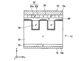
- FIG. 5 is a cross-sectional perspective view of the MOSFET of the first embodiment.
- FIG. 2 is a cross-sectional view taken along the plane II of FIG.
- FIG. 3 is a cross-sectional view taken along the plane III of FIG.
- FIG. 2 is a cross-sectional view taken along the plane IV of FIG.
- FIG. 5 is a cross-sectional view taken along the plane V of FIG.
- the semiconductor substrate is made of silicon carbide and may satisfy Q> 1.49 ⁇ 10 13.
- a plurality of the trenches are provided on the upper surface of the semiconductor substrate, a plurality of the connection regions are provided, and a plurality of the first electric field relaxation regions are provided. It further has a plurality of p-type second electric field relaxation regions, each of which is located below the corresponding trench so that each connection region intersects the plurality of trenches. Each of the second electric field relaxation regions is arranged below the corresponding connection region, is connected to the corresponding connection region, and intersects the plurality of first electric field relaxation regions. It may extend to.
- the electric field is suppressed from being concentrated near the lower end of the connection region when the switching element is off.
- the first electric field relaxation region and the second electric field relaxation region are arranged in a grid pattern in a plan view. Therefore, when the switching element is turned off, the depletion layer rapidly spreads from the first electric field relaxation region and the second electric field relaxation region in the drift region surrounded by the first electric field relaxation region and the second electric field relaxation region. In this way, since the depletion layer spreads rapidly in the drift region, the capacitance between the drain and the source of the switching element can be reduced.
- the p-type impurity concentration in the connection region may be higher than the p-type impurity concentration in the first electric field relaxation region.
- the electric field is more likely to be concentrated in the vicinity of the portion where the connection region and the first electric field relaxation region are connected. Therefore, avalanche breakdown can occur in the vicinity of the portion where the connection region and the first electric field relaxation region are connected.
- FIGS. 1 to 5 show MOSFETs (metal-oxide-semiconductor field effect transistors) 10 of the embodiment.
- the MOSFET 10 has a semiconductor substrate 12.
- one direction parallel to the upper surface 12a of the semiconductor substrate 12 is referred to as the x direction
- the direction parallel to the upper surface 12a and orthogonal to the x direction is referred to as the y direction
- the thickness direction of the semiconductor substrate 12 is referred to as the z direction.
- electrodes, an insulating film, and the like are provided on the upper surface 12a of the semiconductor substrate 12. Note that in FIG. 1, for the sake of explanation, the configuration on the upper surface 12a of the semiconductor substrate 12 is not shown.
- the semiconductor substrate 12 is made of silicon carbide (SiC).
- a plurality of trenches 22 are provided on the upper surface 12a of the semiconductor substrate 12. As shown in FIG. 1, the plurality of trenches 22 extend parallel to each other on the upper surface 12a. The plurality of trenches 22 extend linearly long in the y direction. The plurality of trenches 22 are arranged at intervals in the x direction.
- a gate insulating film 24 and a gate electrode 26 are arranged inside each trench 22.
- the gate insulating film 24 covers the inner surface of the trench 22.
- the gate insulating film 24 has a side insulating film 24a that covers the side surface of the trench 22 and a bottom insulating film 24b that covers the bottom surface of the trench 22.
- the gate insulating film 24 is made of, for example, silicon oxide.
- the gate electrode 26 is arranged in the trench 22.
- the gate electrode 26 is insulated from the semiconductor substrate 12 by the gate insulating film 24. As shown in FIGS. 2, 3 and 5, the upper surface of the gate electrode 26 is covered with the interlayer insulating film 28.
- a source electrode 70 is arranged on the upper surface 12a of the semiconductor substrate 12.
- the source electrode 70 covers the upper surface 12a and the interlayer insulating film 28.
- the source electrode 70 is in contact with the upper surface 12a of the semiconductor substrate 12 at a portion where the interlayer insulating film 28 is not provided.
- the source electrode 70 is insulated from the gate electrode 26 by an interlayer insulating film 28.
- a drain electrode 72 is arranged on the lower surface 12b of the semiconductor substrate 12. The drain electrode 72 is in contact with the lower surface 12b of the semiconductor substrate 12.
- a plurality of source regions 30, a body region 32, a drift region 34, a drain region 35, a plurality of first electric field relaxation regions 36, and a plurality of connection regions 38 are inside the semiconductor substrate 12. It is provided.
- Each source area 30 is an n-type area. As shown in FIGS. 1 and 2, a plurality of source regions 30 are arranged in each of the semiconductor regions (hereinafter, referred to as inter-trench regions) sandwiched between the adjacent trenches 22. As shown in FIGS. 1 and 4, a plurality of source regions 30 are arranged at intervals in the y direction in each inter-trench region. As shown in FIGS. 2 and 4, each source region 30 is arranged in a range facing the upper surface 12a of the semiconductor substrate 12 and is in ohmic contact with the source electrode 70. Each source region 30 is in contact with two trenches 22 located on either side of the inter-trench region. Each source region 30 is in contact with the side insulating film 24a at the upper end of the trench 22.
- the body region 32 is a p-type region.
- the body region 32 has a plurality of contact regions 32a and a main body region 32b.
- Each contact region 32a is a p-type region having a high p-type impurity concentration. As shown in FIGS. 1 and 3, each contact region 32a is provided in the inter-trench region. Each contact region 32a is arranged in a range facing the upper surface 12a of the semiconductor substrate 12. A plurality of contact regions 32a are arranged in each inter-trench region. As shown in FIGS. 1 and 4, in each inter-trench region, the source region 30 and the contact region 32a are alternately arranged in the y direction. Therefore, the contact region 32a is located between the two source regions 30. Each contact region 32a is in ohmic contact with the source electrode 70.
- the main body region 32b is a p-type region having a lower p-type impurity concentration than each contact region 32a. As shown in FIGS. 1 to 4, the main body region 32b is arranged below each source region 30 and each contact region 32a. The main body region 32b is in contact with each source region 30 and each contact region 32a from below. The main body region 32b is distributed over the entire area below each source region 30 and each contact region 32a. As shown in FIGS. 2 and 3, the main body region 32b is in contact with the side insulating film 24a on the lower side of the source region 30. The lower end of the main body region 32b is arranged above the lower end of the gate electrode 26.
- connection regions 38 extending downward from the main body region 32b are provided below the contact region 32a.
- Each connection region 38 extends below the lower end of the trench 22.
- the connection area 38 is not provided in the lower part of the source area 30.
- the connection region 38 extends in the direction (x direction) intersecting the trench 22.
- a plurality of connection regions 38 are arranged at intervals in the y direction, similarly to the contact region 32a.
- the p-type impurity concentration in each connection region 38 is higher than the p-type impurity concentration in the main body region 32b.
- the drift region 34 is an n-type region having a low n-type impurity concentration. As shown in FIGS. 1 to 4, the drift region 34 is arranged below the body region 32 (more specifically, the main body region 32b) and the connection region 38. The drift region 34 is in contact with the main body region 32b and the connection region 38 from below. Further, as shown in FIG. 4, the drift region 34 is also distributed in a region sandwiched between two connecting regions 38 adjacent to each other in the y direction. That is, in the cross section shown in FIG. 4, the drift region 34 is in contact with the connection region 38 from the side. The drift region 34 is separated from each source region 30 by a main body region 32b. As shown in FIGS.
- the drift region 34 is distributed from the inter-trench region to the region below each trench 22. As shown in FIG. 2, the drift region 34 is in contact with the side insulating film 24a on the lower side of the main body region 32b. Further, the drift region 34 is in contact with the bottom insulating film 24b within a range in which the connection region 38 does not exist. Below the lower end of the connection region 38, the drift region 34 is distributed over substantially the entire semiconductor substrate 12 in the x and y directions.
- the drain region 35 is an n-type region having a higher n-type impurity concentration than the drift region 34. As shown in FIGS. 1 to 5, the drain region 35 is arranged below the drift region 34. The drain region 35 is in contact with the drift region 34 from below. The drain region 35 is provided in a range facing the lower surface 12b of the semiconductor substrate 12, and is in ohmic contact with the drain electrode 72.
- Each first electric field relaxation region 36 is a p-type region.
- the p-type impurity concentration in each first electric field relaxation region 36 is lower than the p-type impurity concentration in the connection region 38.
- Each first electric field relaxation region 36 is arranged inside the drift region 34. As shown in FIGS. 1 to 3, each first electric field relaxation region 36 is arranged in the lower part of the trench 22 at a distance from the bottom surface of the corresponding trench 22. As shown in FIGS. 1 and 5, each first electric field relaxation region 36 extends long in the y direction along the bottom surface of the corresponding trench 22. As shown in FIGS. 2 and 5, in the range where the connection region 38 does not exist, the circumference of the first electric field relaxation region 36 is surrounded by the drift region 34.
- a drift region 34 is arranged at a distance between the bottom surface of the trench 22 and the first electric field relaxation region 36.
- the first electric field relaxation region 36 is in contact with the drift region 34 on its upper surface, side surface and lower surface.
- the first electric field relaxation region 36 is connected to the lower end of the connection region 38. That is, each connection region 38 projects downward from the main body region 32b so as to reach each first electric field relaxation region 36.
- the lower end of each first electric field relaxation region 36 is arranged below the lower end of each connection region 38. As described above, the upper end of the connection area 38 is connected to the main body area 32b.
- the first electric field relaxation region 36 is connected to the main body region 32b via the connection region 38. Therefore, the first electric field relaxation region 36 is connected to the source electrode 70 via the connection region 38, the main body region 32b, and the contact region 32a. Therefore, the potential of the first electric field relaxation region 36 is substantially equal to the potential of the source electrode 70.
- the MOSFET 10 of this embodiment is configured to satisfy the relationship of Q> ⁇ ⁇ Ec / e.
- the symbol ⁇ represents the dielectric constant (F / cm) of the connection region 38.
- the symbol Ec represents the seaside electric field strength (V / cm) of the connection region 38.
- the symbol e represents an elementary charge (C).
- the symbol Q is a p-type impurity when the connection region 38 located at the lower part of the trench 22 (that is, the connection region 38 of the portion located between the first electric field relaxation region 36 and the bottom surface of the trench 22) is viewed in a plan view from above. Represents the surface density Q (cm -2 ) of.
- the surface density Q is equal to the value obtained by integrating the p-type impurity concentration (cm -3 ) of the connection region 38 located at the lower part of the trench 22 in the z direction.
- the MOSFET 10 When the MOSFET 10 is used, a potential higher than that of the source electrode 70 is applied to the drain electrode 72. When a voltage equal to or higher than the gate threshold is applied to the gate electrode 26, a channel is formed in the main body region 32b in the range in contact with the gate insulating film 24, and the switching element 10 is turned on. When the voltage applied to the gate electrode 26 is lowered below the gate threshold, the channel disappears and the MOSFET 10 is turned off.
- the potential of the drain electrode 72 is much higher than the potential of the source electrode 70.
- the drift region 34 has a potential close to that of the drain electrode 72.
- the first electric field relaxation region 36 has a potential substantially equal to that of the source electrode 70. Therefore, a high reverse voltage is applied to the pn junction at the interface between the drift region 34 and the first electric field relaxation region 36. Therefore, the depletion layer extends over a wide area from the first electric field relaxation region 36 to the drift region 34. As a result, the withstand voltage of the MOSFET 10 is ensured.
- the depletion layer 80 (dot-hatched region) is also contained in the p-type region (that is, the first electric field relaxation region 36, the connection region 38, and the body region 32).
- the depletion layer 80 spreads over substantially the entire area of the first electric field relaxation region 36, and the depletion layer 80 extends from the drift region 34 to a part of the main body region 32b.
- the depletion layer 80 extends into the inside of the p-type region following the interface between the p-type region (connection region 38 and main body region 32b) and the drift region 34.
- the p-type impurity concentration in the connection region 38 is higher than the p-type impurity concentration in the first electric field relaxation region 36. Therefore, the connection region 38 is less likely to be depleted than the first electric field relaxation region 36. Further, since the p-type impurity concentration in the connection region 38 is high, the first electric field relaxation region 36 in the range adjacent to the connection region 38 is less likely to be depleted than the first electric field relaxation region 36 in the other range. Therefore, as shown in FIGS. 3 and 5, the depletion layer 80 is curved in the range where both the first electric field relaxation region 36 and the connection region 38 are provided. That is, the non-depletion region remains in the first electric field relaxation region 36 located below the connection region 38.
- the equipotential lines are curved in the lower part of the connection region 38, and the distance between the equipotential lines becomes narrow.
- the electric field is concentrated in the vicinity of the portion where the connection region 38 and the first electric field relaxation region 36 are connected. Therefore, avalanche breakdown is likely to occur in the vicinity of the portion where the connection region 38 and the first electric field relaxation region 36 are connected.
- the holes generated due to the avalanche breakdown flow to the source electrode 70 via the connection region 38 and the body region 32.
- the depletion layer 80 extending over the connection region 38 does not reach the lower end of the trench 22.
- the depletion layer 80 does not reach the lower end of the trench 22. Therefore, a non-depleted region remains in the connecting region 38 around the lower end of the trench 22. In the non-depleted region, the moving speed of the hole is slower than in the depleted region. Therefore, the non-depleted region suppresses the injection of holes flowing through the connection region 38 (holes generated in the vicinity of the connection region 38 by avalanche breakdown) into the gate insulating film 24, and most of the holes are the source electrode 70. Flow to. Therefore, in this MOSFET 10, even when an avalanche breakdown occurs, it is possible to suppress a change in the characteristics of the gate insulating film 24.
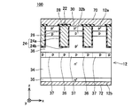
- Example 2 shows the MOSFET 100 of the second embodiment.
- FIG. 6 shows a cross section corresponding to FIG. 3 of the first embodiment
- FIG. 7 shows a cross section corresponding to FIG. 4 of the first embodiment.
- FIG. 8 shows a plan view of the semiconductor substrate 12 from above.
- the same components as in the first embodiment are designated by the same reference numerals, and the description thereof will be omitted.
- the MOSFET 10 of the second embodiment has a plurality of second electric field relaxation regions 37 inside the semiconductor substrate 12. In FIG. 8, the first electric field relaxation region 36 and the second electric field relaxation region 37 are shown by hatching.
- each second electric field relaxation zone 37 is arranged below the corresponding connection zone 38. Each second electric field relaxation zone 37 is connected to the corresponding connection zone 38. The upper end of each second electric field relaxation zone 37 is connected to the lower end of the corresponding connection zone 38. As shown in FIG. 6, each second electric field relaxation region 37 is arranged at substantially the same depth as each first electric field relaxation region 36. As shown in FIGS. 6 and 8, each second electric field relaxation region 37 extends so as to intersect the plurality of first electric field relaxation regions 36. That is, each second electric field relaxation region 37 extends in the x direction along the lower end of the corresponding connection region 38. Each second electric field relaxation region 37 connects a plurality of first electric field relaxation regions 36 to each other. That is, as shown in FIG. 8, each first electric field relaxation region 36 and each second electric field relaxation region 37 are arranged in a grid pattern when viewed in a plan view. Each second electric field relaxation region 37 has substantially the same p-type impurity concentration as each first electric field relaxation region 36.
- a second electric field relaxation region 37 having a lower p-type impurity concentration than the connection region 38 is arranged below the connection region 38. Therefore, in the state where the MOSFET 100 is off, the second electric field relaxation region 37 is depleted, and the electric field applied to the connection region 38 is relaxed. Further, the first electric field relaxation region 36 and the second electric field relaxation region 37 are arranged in a grid pattern in a plan view. Therefore, in the drift region 34 surrounded by the first electric field relaxation region 36 and the second electric field relaxation region 37 and the drift region 34 in the inter-trench region located above the drift region 34, the first electric field relaxation region 36 and the second electric field relaxation region 36 The depletion layer spreads rapidly from region 37.
- the depletion layer rapidly spreads in the drift region 34, so that the capacity between the drain and the source of the MOSFET 100 is reduced.
- the output capacitance of the MOSFET 100 can be reduced, and the loss caused by the MOSFET 100 can be reduced.
- the recovery loss can be reduced.
- connection area 38 was provided below the contact area 32a.
- connection area 38 may not be provided below the contact area 32a, for example, may be provided below the source area 30.
- the semiconductor substrate 12 was made of silicon carbide.
- the semiconductor substrate 12 may be made of other semiconductor materials such as silicon (Si) and gallium nitride (GaN).
- the surface density Q may be appropriately set based on the dielectric constant of the material to be used and the strength of the coastal electric field.
Abstract
This switching element comprises: a semiconductor substrate in which a trench is provided; a gate insulating film; and a gate electrode. The semiconductor substrate has a source region, a body region, a drift region, a first electric field relaxation region, and a connection region. The drift region contacts the gate insulating film at the side surface of the trench and the bottom surface of the trench on the underside of the body region. The first electric field relaxation region is placed inside the drift region, and is placed at the bottom of the trench with a gap opened from the bottom surface of the trench, and extends along the bottom surface of the trench. The connection region projects downward from the body region so as to reach the first electric field relaxation region, and extends long in the direction intersecting the trench when seen in plan view from above. When the dielectric constant of the connection region is ε (F/cm), the critical electric field strength of the connection region is Ec (V/cm), the quantum of electricity is e(C), and the surface density of the p-type impurity when the connection region positioned at the bottom part of the trench is seen in plan view from above is Q(cm–2), Q > ε • Ec/e is satisfied.
Description
本明細書に開示の技術は、スイッチング素子に関する。
The techniques disclosed herein relate to switching elements.
日本公開特許公報第2009-158681号に開示のスイッチング素子は、半導体基板とゲート電極を有している。半導体基板の上面には、トレンチが設けられている。トレンチ内に、ゲート電極が配置されている。ゲート電極は、ゲート絶縁膜によって半導体基板から絶縁されている。半導体基板は、ソース領域と、ボディ領域と、ドリフト領域と、電界緩和領域(底部領域)を有する。ソース領域は、トレンチの側面でゲート絶縁膜に接するn型領域である。ボディ領域は、ソース領域の下側のトレンチの側面でゲート絶縁膜に接するp型領域である。ドリフト領域は、ボディ領域の下側に配置されており、ボディ領域の下側のトレンチの側面とトレンチの底面でゲート絶縁膜に接しているn型領域である。電界緩和領域は、ドリフト領域の内部に配置されており、トレンチの底面から間隔を空けてトレンチの下部に配置されているp型領域である。
The switching element disclosed in Japanese Patent Publication No. 2009-158681 has a semiconductor substrate and a gate electrode. A trench is provided on the upper surface of the semiconductor substrate. A gate electrode is arranged in the trench. The gate electrode is insulated from the semiconductor substrate by a gate insulating film. The semiconductor substrate has a source region, a body region, a drift region, and an electric field relaxation region (bottom region). The source region is an n-type region in contact with the gate insulating film on the side surface of the trench. The body region is a p-shaped region in contact with the gate insulating film on the side surface of the trench below the source region. The drift region is an n-type region that is arranged below the body region and is in contact with the gate insulating film at the side surface of the trench below the body region and the bottom surface of the trench. The electric field relaxation region is a p-type region that is arranged inside the drift region and is arranged at the bottom of the trench at a distance from the bottom surface of the trench.
特許文献1のスイッチング素子では、アバランシェ降伏が生じた場合に、電界緩和領域近傍で発生するホールの一部が、ドリフト領域からボディ領域へ向かって流れる過程でゲート絶縁膜に注入される。これにより、ゲート絶縁膜の特性が変化し、ゲート閾値が変動するといった問題が生じる。本明細書では、アバランシェ降伏が生じた場合に、ゲート絶縁膜の特性変化を抑制することができる技術を提案する。
In the switching element of Patent Document 1, when avalanche breakdown occurs, a part of the holes generated in the vicinity of the electric field relaxation region is injected into the gate insulating film in the process of flowing from the drift region to the body region. This causes a problem that the characteristics of the gate insulating film change and the gate threshold value fluctuates. The present specification proposes a technique capable of suppressing a change in the characteristics of the gate insulating film when an avalanche breakdown occurs.
本明細書が開示するスイッチング素子は、上面にトレンチが設けられた半導体基板と、前記トレンチの内面を覆うゲート絶縁膜と、前記トレンチ内に配置されており、前記ゲート絶縁膜によって前記半導体基板から絶縁されているゲート電極を備えている。前記半導体基板が、ソース領域と、ボディ領域と、ドリフト領域と、第1電界緩和領域と、接続領域を有している。前記ソース領域は、前記トレンチの側面で前記ゲート絶縁膜に接するn型領域である。前記ボディ領域は、前記ソース領域の下側の前記側面で前記ゲート絶縁膜に接するp型領域である。前記ドリフト領域は、前記ボディ領域の下側に配置されており、前記ボディ領域の下側の前記側面で前記ゲート絶縁膜に接しており、前記トレンチの底面で前記ゲート絶縁膜に接しているn型領域である。前記第1電界緩和領域は、前記ドリフト領域の内部に配置されており、前記トレンチの前記底面から間隔を空けて前記トレンチの下部に配置されており、前記トレンチの前記底面に沿って伸びているp型領域である。前記接続領域は、前記第1電界緩和領域に達するように前記ボディ領域から下側に突出しており、上から平面視したときに前記トレンチと交差する方向に長く伸びているp型領域である。前記接続領域の誘電率をε(F/cm)、前記接続領域の臨海電界強度をEc(V/cm)、電気素量をe(C)、前記トレンチの下部に位置する前記接続領域を上から平面視したときのp型不純物の面密度をQ(cm-2)としたときに、Q>ε・Ec/eを満たす。
The switching element disclosed in the present specification is arranged in a semiconductor substrate having a trench on the upper surface, a gate insulating film covering the inner surface of the trench, and the gate insulating film from the semiconductor substrate. It has an insulated gate electrode. The semiconductor substrate has a source region, a body region, a drift region, a first electric field relaxation region, and a connection region. The source region is an n-type region in contact with the gate insulating film on the side surface of the trench. The body region is a p-type region in contact with the gate insulating film on the side surface below the source region. The drift region is arranged below the body region, is in contact with the gate insulating film at the side surface below the body region, and is in contact with the gate insulating film at the bottom surface of the trench. It is a type area. The first electric field relaxation region is arranged inside the drift region, is arranged at the lower part of the trench at a distance from the bottom surface of the trench, and extends along the bottom surface of the trench. It is a p-type region. The connection region is a p-type region that protrudes downward from the body region so as to reach the first electric field relaxation region and extends long in a direction intersecting the trench when viewed in a plan view from above. The permittivity of the connection region is ε (F / cm), the seaside electric field strength of the connection region is Ec (V / cm), the elementary charge is e (C), and the connection region located below the trench is above. When the surface density of p-type impurities is Q (cm -2 ) when viewed from above, Q> ε · Ec / e is satisfied.
このスイッチング素子がオフするときには、接続領域と第1電界緩和領域が繋がっている部分で電界が集中し易い。このため、このスイッチング素子では、接続領域と第1電界緩和領域が繋がっている部分の近傍でアバランシェ降伏が生じる。アバランシェ降伏で生じたホールは、接続領域を介してボディ領域へ流れる。また、このスイッチング素子では、面密度Qが上式を満たすので、接続領域内に広がる空乏層がトレンチの下端まで達しない。すなわち、トレンチの下端の周辺の接続領域内に非空乏化領域(空乏層が広がっていない領域)が残存する。非空乏化領域によって、接続領域を流れるホール(アバランシェ降伏によって生じたホール)がゲート絶縁膜に注入されることが抑制される。したがって、上記のスイッチング素子では、アバランシェ降伏が生じた場合であっても、ゲート絶縁膜の特性変化を抑制することができる。
When this switching element is turned off, the electric field tends to concentrate in the portion where the connection region and the first electric field relaxation region are connected. Therefore, in this switching element, avalanche breakdown occurs in the vicinity of the portion where the connection region and the first electric field relaxation region are connected. The holes created by the avalanche breakdown flow through the contiguous zone to the body region. Further, in this switching element, since the surface density Q satisfies the above equation, the depletion layer spreading in the connection region does not reach the lower end of the trench. That is, a non-depleted region (a region in which the depletion layer does not spread) remains in the connecting region around the lower end of the trench. The non-depleted region prevents holes flowing through the contiguous zone (holes created by avalanche breakdown) from being injected into the gate insulating film. Therefore, in the above-mentioned switching element, it is possible to suppress a change in the characteristics of the gate insulating film even when an avalanche breakdown occurs.
本明細書が開示する技術要素について、以下に列記する。なお、以下の各技術要素は、それぞれ独立して有用なものである。
The technical elements disclosed in this specification are listed below. The following technical elements are useful independently.
本明細書が開示する一例の構成では、前記半導体基板が炭化シリコンにより構成されており、Q>1.49×10¹³を満たしてもよい。
In one example configuration disclosed herein, the semiconductor substrate is made of silicon carbide and may satisfy Q> 1.49 × 10 13.
本明細書が開示する一例の構成では、前記半導体基板の前記上面に前記トレンチが複数設けられており、前記接続領域が複数設けられており、前記第1電界緩和領域が複数設けられており、p型の複数の第2電界緩和領域をさらに有し、前記各第1電界緩和領域が、対応する前記トレンチの下部に配置されており、前記各接続領域が、前記複数のトレンチと交差するように伸びており、前記各第2電界緩和領域が、対応する前記接続領域の下部に配置されており、対応する前記接続領域に接続されており、前記複数の第1電界緩和領域と交差するように伸びていてもよい。
In the configuration of one example disclosed in the present specification, a plurality of the trenches are provided on the upper surface of the semiconductor substrate, a plurality of the connection regions are provided, and a plurality of the first electric field relaxation regions are provided. It further has a plurality of p-type second electric field relaxation regions, each of which is located below the corresponding trench so that each connection region intersects the plurality of trenches. Each of the second electric field relaxation regions is arranged below the corresponding connection region, is connected to the corresponding connection region, and intersects the plurality of first electric field relaxation regions. It may extend to.
このような構成では、スイッチング素子がオフしている状態において、接続領域の下端近傍に電界が集中することが抑制される。さらに、第1電界緩和領域及び第2電界緩和領域が、平面視において格子状に配置される。このため、スイッチング素子がオフするときに、第1電界緩和領域及び第2電界緩和領域によって囲まれたドリフト領域に、第1電界緩和領域及び第2電界緩和領域から空乏層が迅速に広がる。このように、ドリフト領域内に空乏層が迅速に広がるので、スイッチング素子のドレイン-ソース間の容量を低減することができる。
In such a configuration, the electric field is suppressed from being concentrated near the lower end of the connection region when the switching element is off. Further, the first electric field relaxation region and the second electric field relaxation region are arranged in a grid pattern in a plan view. Therefore, when the switching element is turned off, the depletion layer rapidly spreads from the first electric field relaxation region and the second electric field relaxation region in the drift region surrounded by the first electric field relaxation region and the second electric field relaxation region. In this way, since the depletion layer spreads rapidly in the drift region, the capacitance between the drain and the source of the switching element can be reduced.
本明細書が開示する一例の構成では、前記接続領域のp型不純物濃度が、前記第1電界緩和領域のp型不純物濃度よりも高くてもよい。
In the configuration of one example disclosed in the present specification, the p-type impurity concentration in the connection region may be higher than the p-type impurity concentration in the first electric field relaxation region.
このような構成では、接続領域と第1電界緩和領域が繋がっている部分の近傍で電界がより集中し易い。このため、接続領域と第1電界緩和領域が繋がっている部分の近傍でアバランシェ降伏を生じさせることができる。
In such a configuration, the electric field is more likely to be concentrated in the vicinity of the portion where the connection region and the first electric field relaxation region are connected. Therefore, avalanche breakdown can occur in the vicinity of the portion where the connection region and the first electric field relaxation region are connected.
(実施例1)
図1~5は、実施形態のMOSFET(metal-oxide-semiconductor field effect transistor)10を示している。MOSFET10は、半導体基板12を有している。以下では、半導体基板12の上面12aと平行な一方向をx方向といい、上面12aに平行でx方向に直行する方向をy方向といい、半導体基板12の厚み方向をz方向という。図2~5に示すように、半導体基板12の上面12a上には、電極、絶縁膜等が設けられている。なお、図1では、説明のため、半導体基板12の上面12a上の構成の図示を省略している。 (Example 1)
FIGS. 1 to 5 show MOSFETs (metal-oxide-semiconductor field effect transistors) 10 of the embodiment. TheMOSFET 10 has a semiconductor substrate 12. In the following, one direction parallel to the upper surface 12a of the semiconductor substrate 12 is referred to as the x direction, the direction parallel to the upper surface 12a and orthogonal to the x direction is referred to as the y direction, and the thickness direction of the semiconductor substrate 12 is referred to as the z direction. As shown in FIGS. 2 to 5, electrodes, an insulating film, and the like are provided on the upper surface 12a of the semiconductor substrate 12. Note that in FIG. 1, for the sake of explanation, the configuration on the upper surface 12a of the semiconductor substrate 12 is not shown.
図1~5は、実施形態のMOSFET(metal-oxide-semiconductor field effect transistor)10を示している。MOSFET10は、半導体基板12を有している。以下では、半導体基板12の上面12aと平行な一方向をx方向といい、上面12aに平行でx方向に直行する方向をy方向といい、半導体基板12の厚み方向をz方向という。図2~5に示すように、半導体基板12の上面12a上には、電極、絶縁膜等が設けられている。なお、図1では、説明のため、半導体基板12の上面12a上の構成の図示を省略している。 (Example 1)
FIGS. 1 to 5 show MOSFETs (metal-oxide-semiconductor field effect transistors) 10 of the embodiment. The
半導体基板12は、炭化シリコン(SiC)によって構成されている。半導体基板12の上面12aには、複数のトレンチ22が設けられている。図1に示すように、複数のトレンチ22は、上面12aにおいて、互いに平行に伸びている。複数のトレンチ22は、y方向に直線状に長く伸びている。複数のトレンチ22は、x方向に間隔を空けて配列されている。各トレンチ22の内部に、ゲート絶縁膜24とゲート電極26が配置されている。
The semiconductor substrate 12 is made of silicon carbide (SiC). A plurality of trenches 22 are provided on the upper surface 12a of the semiconductor substrate 12. As shown in FIG. 1, the plurality of trenches 22 extend parallel to each other on the upper surface 12a. The plurality of trenches 22 extend linearly long in the y direction. The plurality of trenches 22 are arranged at intervals in the x direction. A gate insulating film 24 and a gate electrode 26 are arranged inside each trench 22.
ゲート絶縁膜24は、トレンチ22の内面を覆っている。ゲート絶縁膜24は、トレンチ22の側面を覆う側面絶縁膜24aと、トレンチ22の底面を覆う底面絶縁膜24bを有している。ゲート絶縁膜24は、例えば、酸化シリコンにより構成されている。
The gate insulating film 24 covers the inner surface of the trench 22. The gate insulating film 24 has a side insulating film 24a that covers the side surface of the trench 22 and a bottom insulating film 24b that covers the bottom surface of the trench 22. The gate insulating film 24 is made of, for example, silicon oxide.
ゲート電極26は、トレンチ22内に配置されている。ゲート電極26は、ゲート絶縁膜24によって半導体基板12から絶縁されている。図2、3及び5に示すように、ゲート電極26の上面は、層間絶縁膜28によって覆われている。
The gate electrode 26 is arranged in the trench 22. The gate electrode 26 is insulated from the semiconductor substrate 12 by the gate insulating film 24. As shown in FIGS. 2, 3 and 5, the upper surface of the gate electrode 26 is covered with the interlayer insulating film 28.
半導体基板12の上面12aには、ソース電極70が配置されている。ソース電極70は、上面12aと層間絶縁膜28を覆っている。ソース電極70は、層間絶縁膜28が設けられていない部分で半導体基板12の上面12aに接している。ソース電極70は、層間絶縁膜28によってゲート電極26から絶縁されている。半導体基板12の下面12bには、ドレイン電極72が配置されている。ドレイン電極72は、半導体基板12の下面12bに接している。
A source electrode 70 is arranged on the upper surface 12a of the semiconductor substrate 12. The source electrode 70 covers the upper surface 12a and the interlayer insulating film 28. The source electrode 70 is in contact with the upper surface 12a of the semiconductor substrate 12 at a portion where the interlayer insulating film 28 is not provided. The source electrode 70 is insulated from the gate electrode 26 by an interlayer insulating film 28. A drain electrode 72 is arranged on the lower surface 12b of the semiconductor substrate 12. The drain electrode 72 is in contact with the lower surface 12b of the semiconductor substrate 12.
図1に示すように、半導体基板12の内部には、複数のソース領域30、ボディ領域32、ドリフト領域34、ドレイン領域35、複数の第1電界緩和領域36、及び、複数の接続領域38が設けられている。
As shown in FIG. 1, a plurality of source regions 30, a body region 32, a drift region 34, a drain region 35, a plurality of first electric field relaxation regions 36, and a plurality of connection regions 38 are inside the semiconductor substrate 12. It is provided.
各ソース領域30は、n型領域である。図1及び図2に示すように、隣接するトレンチ22に挟まれた半導体領域(以下、トレンチ間領域という。)のそれぞれに、複数のソース領域30が配置されている。図1及び図4に示すように、各トレンチ間領域において、複数のソース領域30がy方向に間隔を空けて配置されている。図2及び図4に示すように、各ソース領域30は、半導体基板12の上面12aに臨む範囲に配置されており、ソース電極70にオーミック接触している。各ソース領域30は、トレンチ間領域の両側に位置する2つのトレンチ22に接している。各ソース領域30は、トレンチ22の上端部において、側面絶縁膜24aに接している。
Each source area 30 is an n-type area. As shown in FIGS. 1 and 2, a plurality of source regions 30 are arranged in each of the semiconductor regions (hereinafter, referred to as inter-trench regions) sandwiched between the adjacent trenches 22. As shown in FIGS. 1 and 4, a plurality of source regions 30 are arranged at intervals in the y direction in each inter-trench region. As shown in FIGS. 2 and 4, each source region 30 is arranged in a range facing the upper surface 12a of the semiconductor substrate 12 and is in ohmic contact with the source electrode 70. Each source region 30 is in contact with two trenches 22 located on either side of the inter-trench region. Each source region 30 is in contact with the side insulating film 24a at the upper end of the trench 22.
ボディ領域32は、p型領域である。ボディ領域32は、複数のコンタクト領域32aと、メインボディ領域32bを有している。
The body region 32 is a p-type region. The body region 32 has a plurality of contact regions 32a and a main body region 32b.
各コンタクト領域32aは、p型不純物濃度が高いp型領域である。図1及び図3に示すように、各コンタクト領域32aは、トレンチ間領域に設けられている。各コンタクト領域32aは、半導体基板12の上面12aに臨む範囲に配置されている。各トレンチ間領域に、複数のコンタクト領域32aが配置されている。図1及び図4に示すように、各トレンチ間領域において、ソース領域30とコンタクト領域32aが、y方向に交互に配置されている。したがって、コンタクト領域32aは、2つのソース領域30の間に配置されている。各コンタクト領域32aは、ソース電極70にオーミック接触している。
Each contact region 32a is a p-type region having a high p-type impurity concentration. As shown in FIGS. 1 and 3, each contact region 32a is provided in the inter-trench region. Each contact region 32a is arranged in a range facing the upper surface 12a of the semiconductor substrate 12. A plurality of contact regions 32a are arranged in each inter-trench region. As shown in FIGS. 1 and 4, in each inter-trench region, the source region 30 and the contact region 32a are alternately arranged in the y direction. Therefore, the contact region 32a is located between the two source regions 30. Each contact region 32a is in ohmic contact with the source electrode 70.
メインボディ領域32bは、各コンタクト領域32aよりもp型不純物濃度が低いp型領域である。図1~4に示すように、メインボディ領域32bは、各ソース領域30及び各コンタクト領域32aの下側に配置されている。メインボディ領域32bは、各ソース領域30及び各コンタクト領域32aに対して下側から接している。メインボディ領域32bは、各ソース領域30及び各コンタクト領域32aの下側の全域に分布している。図2及び図3に示すように、メインボディ領域32bは、ソース領域30の下側で側面絶縁膜24aに接している。メインボディ領域32bの下端は、ゲート電極26の下端よりも上側に配置されている。
The main body region 32b is a p-type region having a lower p-type impurity concentration than each contact region 32a. As shown in FIGS. 1 to 4, the main body region 32b is arranged below each source region 30 and each contact region 32a. The main body region 32b is in contact with each source region 30 and each contact region 32a from below. The main body region 32b is distributed over the entire area below each source region 30 and each contact region 32a. As shown in FIGS. 2 and 3, the main body region 32b is in contact with the side insulating film 24a on the lower side of the source region 30. The lower end of the main body region 32b is arranged above the lower end of the gate electrode 26.
図3及び図4に示すように、コンタクト領域32aの下部には、メインボディ領域32bから下側に伸びる複数の接続領域38が設けられている。各接続領域38は、トレンチ22の下端よりも下側まで伸びている。図2及び図4に示すように、ソース領域30の下部には、接続領域38は設けられていない。図3に示すように、接続領域38は、トレンチ22と交差する方向(x方向)に伸びている。図1及び図4に示すように、コンタクト領域32aと同様に、複数の接続領域38が、y方向に間隔を空けて配置されている。各接続領域38のp型不純物濃度は、メインボディ領域32bのp型不純物濃度よりも高い。
As shown in FIGS. 3 and 4, a plurality of connection regions 38 extending downward from the main body region 32b are provided below the contact region 32a. Each connection region 38 extends below the lower end of the trench 22. As shown in FIGS. 2 and 4, the connection area 38 is not provided in the lower part of the source area 30. As shown in FIG. 3, the connection region 38 extends in the direction (x direction) intersecting the trench 22. As shown in FIGS. 1 and 4, a plurality of connection regions 38 are arranged at intervals in the y direction, similarly to the contact region 32a. The p-type impurity concentration in each connection region 38 is higher than the p-type impurity concentration in the main body region 32b.
ドリフト領域34は、n型不純物濃度が低いn型領域である。図1~4に示すように、ドリフト領域34は、ボディ領域32(より詳細には、メインボディ領域32b)及び接続領域38の下側に配置されている。ドリフト領域34は、メインボディ領域32b及び接続領域38に対して下側から接している。また、ドリフト領域34は、図4に示すように、y方向に隣接する2つの接続領域38に挟まれた領域にも分布している。すなわち、図4に示す断面では、ドリフト領域34は、接続領域38に対して側方から接している。ドリフト領域34は、メインボディ領域32bによって各ソース領域30から分離されている。図1及び図2に示すように、ドリフト領域34は、各トレンチ間領域から各トレンチ22よりも下側の領域まで分布している。図2に示すように、ドリフト領域34は、メインボディ領域32bの下側で側面絶縁膜24aに接している。また、ドリフト領域34は、接続領域38が存在しない範囲で底面絶縁膜24bに接している。接続領域38の下端よりも下側では、ドリフト領域34は、x方向及びy方向において、半導体基板12の略全域に分布している。
The drift region 34 is an n-type region having a low n-type impurity concentration. As shown in FIGS. 1 to 4, the drift region 34 is arranged below the body region 32 (more specifically, the main body region 32b) and the connection region 38. The drift region 34 is in contact with the main body region 32b and the connection region 38 from below. Further, as shown in FIG. 4, the drift region 34 is also distributed in a region sandwiched between two connecting regions 38 adjacent to each other in the y direction. That is, in the cross section shown in FIG. 4, the drift region 34 is in contact with the connection region 38 from the side. The drift region 34 is separated from each source region 30 by a main body region 32b. As shown in FIGS. 1 and 2, the drift region 34 is distributed from the inter-trench region to the region below each trench 22. As shown in FIG. 2, the drift region 34 is in contact with the side insulating film 24a on the lower side of the main body region 32b. Further, the drift region 34 is in contact with the bottom insulating film 24b within a range in which the connection region 38 does not exist. Below the lower end of the connection region 38, the drift region 34 is distributed over substantially the entire semiconductor substrate 12 in the x and y directions.
ドレイン領域35は、ドリフト領域34よりもn型不純物濃度が高いn型領域である。図1~5に示すように、ドレイン領域35は、ドリフト領域34の下側に配置されている。ドレイン領域35は、ドリフト領域34に対して下側から接している。ドレイン領域35は、半導体基板12の下面12bに臨む範囲に設けられており、ドレイン電極72にオーミック接触している。
The drain region 35 is an n-type region having a higher n-type impurity concentration than the drift region 34. As shown in FIGS. 1 to 5, the drain region 35 is arranged below the drift region 34. The drain region 35 is in contact with the drift region 34 from below. The drain region 35 is provided in a range facing the lower surface 12b of the semiconductor substrate 12, and is in ohmic contact with the drain electrode 72.
各第1電界緩和領域36は、p型領域である。各第1電界緩和領域36のp型不純物濃度は、接続領域38のp型不純物濃度よりも低い。各第1電界緩和領域36は、ドリフト領域34の内部に配置されている。図1~図3に示すように、各第1電界緩和領域36は、対応するトレンチ22の底面から間隔を空けてトレンチ22の下部に配置されている。図1及び図5に示すように、各第1電界緩和領域36は、対応するトレンチ22の底面に沿ってy方向に長く伸びている。図2及び図5に示すように、接続領域38が存在しない範囲では、第1電界緩和領域36の周囲は、ドリフト領域34によって囲まれている。このため、トレンチ22の底面と第1電界緩和領域36の間の間隔には、ドリフト領域34が配置されている。図2に示す断面では、第1電界緩和領域36は、その上面、側面及び下面において、ドリフト領域34と接している。図3に示すように、接続領域38の下部では、第1電界緩和領域36は、接続領域38の下端に接続されている。すなわち、各接続領域38は、各第1電界緩和領域36に達するようにメインボディ領域32bから下側に突出している。各第1電界緩和領域36の下端は、各接続領域38の下端よりも下側に配置されている。上述したように、接続領域38の上端はメインボディ領域32bに接続されている。したがって、接続領域38を介して、第1電界緩和領域36はメインボディ領域32bに接続されている。このため、第1電界緩和領域36は、接続領域38、メインボディ領域32b、及び、コンタクト領域32aを介して、ソース電極70に接続されている。したがって、第1電界緩和領域36の電位は、ソース電極70の電位と略等しい。
Each first electric field relaxation region 36 is a p-type region. The p-type impurity concentration in each first electric field relaxation region 36 is lower than the p-type impurity concentration in the connection region 38. Each first electric field relaxation region 36 is arranged inside the drift region 34. As shown in FIGS. 1 to 3, each first electric field relaxation region 36 is arranged in the lower part of the trench 22 at a distance from the bottom surface of the corresponding trench 22. As shown in FIGS. 1 and 5, each first electric field relaxation region 36 extends long in the y direction along the bottom surface of the corresponding trench 22. As shown in FIGS. 2 and 5, in the range where the connection region 38 does not exist, the circumference of the first electric field relaxation region 36 is surrounded by the drift region 34. Therefore, a drift region 34 is arranged at a distance between the bottom surface of the trench 22 and the first electric field relaxation region 36. In the cross section shown in FIG. 2, the first electric field relaxation region 36 is in contact with the drift region 34 on its upper surface, side surface and lower surface. As shown in FIG. 3, in the lower part of the connection region 38, the first electric field relaxation region 36 is connected to the lower end of the connection region 38. That is, each connection region 38 projects downward from the main body region 32b so as to reach each first electric field relaxation region 36. The lower end of each first electric field relaxation region 36 is arranged below the lower end of each connection region 38. As described above, the upper end of the connection area 38 is connected to the main body area 32b. Therefore, the first electric field relaxation region 36 is connected to the main body region 32b via the connection region 38. Therefore, the first electric field relaxation region 36 is connected to the source electrode 70 via the connection region 38, the main body region 32b, and the contact region 32a. Therefore, the potential of the first electric field relaxation region 36 is substantially equal to the potential of the source electrode 70.
本実施例のMOSFET10は、Q>ε・Ec/eの関係を満たすように構成されている。なお、記号εは、接続領域38の誘電率(F/cm)を表す。記号Ecは、接続領域38の臨海電界強度(V/cm)を表す。記号eは、電気素量(C)を表す。記号Qは、トレンチ22の下部に位置する接続領域38(すなわち、第1電界緩和領域36とトレンチ22の底面の間に位置する部分の接続領域38)を上から平面視したときのp型不純物の面密度Q(cm-2)を表す。面密度Qは、トレンチ22の下部に位置する接続領域38のp型不純物濃度(cm-3)を、z方向に積分した値に等しい。本実施例では、半導体基板12が炭化シリコンによって構成されているので、ε=8.55×10-13(F/cm)であり、Ec=2.8×106(V/cm)である。また、e=1.6×10-19(C)である。したがって、Q>1.49×1013を満たすように、接続領域38の面密度Qが調整されている。
The MOSFET 10 of this embodiment is configured to satisfy the relationship of Q> ε · Ec / e. The symbol ε represents the dielectric constant (F / cm) of the connection region 38. The symbol Ec represents the seaside electric field strength (V / cm) of the connection region 38. The symbol e represents an elementary charge (C). The symbol Q is a p-type impurity when the connection region 38 located at the lower part of the trench 22 (that is, the connection region 38 of the portion located between the first electric field relaxation region 36 and the bottom surface of the trench 22) is viewed in a plan view from above. Represents the surface density Q (cm -2 ) of. The surface density Q is equal to the value obtained by integrating the p-type impurity concentration (cm -3 ) of the connection region 38 located at the lower part of the trench 22 in the z direction. In this embodiment, since the semiconductor substrate 12 is made of silicon carbide, ε = 8.55 × 10⁻¹³ (F / cm) and Ec = 2.8 × 10 6 (V / cm). .. Further, e = 1.6 × 10⁻¹⁹ (C). Therefore, the surface density Q of the connection region 38 is adjusted so as to satisfy Q> 1.49 × 10 13.
MOSFET10の使用時には、ドレイン電極72にソース電極70よりも高い電位が印加される。ゲート電極26にゲート閾値以上の電圧を印加すると、ゲート絶縁膜24に接する範囲のメインボディ領域32bにチャネルが形成され、スイッチング素子10がオンする。ゲート電極26に印加する電圧をゲート閾値未満まで低下させると、チャネルが消失し、MOSFET10がオフする。
When the MOSFET 10 is used, a potential higher than that of the source electrode 70 is applied to the drain electrode 72. When a voltage equal to or higher than the gate threshold is applied to the gate electrode 26, a channel is formed in the main body region 32b in the range in contact with the gate insulating film 24, and the switching element 10 is turned on. When the voltage applied to the gate electrode 26 is lowered below the gate threshold, the channel disappears and the MOSFET 10 is turned off.
MOSFET10がオフしている状態では、ドレイン電極72の電位がソース電極70の電位よりも遥かに高い。この状態では、ドリフト領域34は、ドレイン電極72に近い電位を有する。また、上述したように、第1電界緩和領域36は、ソース電極70と略等しい電位を有する。このため、ドリフト領域34と第1電界緩和領域36の界面のpn接合に高い逆電圧が印加される。したがって、第1電界緩和領域36からドリフト領域34へ、空乏層が広範囲に広がっている。これにより、MOSFET10の耐圧が確保される。
When the MOSFET 10 is off, the potential of the drain electrode 72 is much higher than the potential of the source electrode 70. In this state, the drift region 34 has a potential close to that of the drain electrode 72. Further, as described above, the first electric field relaxation region 36 has a potential substantially equal to that of the source electrode 70. Therefore, a high reverse voltage is applied to the pn junction at the interface between the drift region 34 and the first electric field relaxation region 36. Therefore, the depletion layer extends over a wide area from the first electric field relaxation region 36 to the drift region 34. As a result, the withstand voltage of the MOSFET 10 is ensured.
MOSFET10がオフするときには、ドリフト領域34が空乏化されるとともに、p型領域(すなわち、第1電界緩和領域36、接続領域38、ボディ領域32)内にも空乏層80(ドットハッチングされた領域)が広がる。接続領域38が設けられていない範囲では、図2に示すように、第1電界緩和領域36の略全域に空乏層80が広がるとともに、ドリフト領域34からメインボディ領域32bの一部に空乏層80が伸びる。図4に示すように、p型領域(接続領域38及びメインボディ領域32b)とドリフト領域34の界面に倣って、p型領域の内部へ空乏層80が伸びる。
When the MOSFET 10 is turned off, the drift region 34 is depleted, and the depletion layer 80 (dot-hatched region) is also contained in the p-type region (that is, the first electric field relaxation region 36, the connection region 38, and the body region 32). Spreads. In the range where the connection region 38 is not provided, as shown in FIG. 2, the depletion layer 80 spreads over substantially the entire area of the first electric field relaxation region 36, and the depletion layer 80 extends from the drift region 34 to a part of the main body region 32b. Grow. As shown in FIG. 4, the depletion layer 80 extends into the inside of the p-type region following the interface between the p-type region (connection region 38 and main body region 32b) and the drift region 34.
本実施例のMOSFET10では、接続領域38のp型不純物濃度が、第1電界緩和領域36のp型不純物濃度よりも高い。このため、接続領域38は、第1電界緩和領域36よりも空乏化され難い。また、接続領域38のp型不純物濃度が高いので、接続領域38に隣接する範囲の第1電界緩和領域36は、その他の範囲の第1電界緩和領域36よりも空乏化され難い。したがって、第1電界緩和領域36と接続領域38の双方が設けられている範囲では、図3及び図5に示すように、空乏層80が湾曲する。すなわち、接続領域38の下部に位置する第1電界緩和領域36内に非空乏化領域が残存する。その結果、接続領域38の下部において等電位線が湾曲し、等電位線同士の間隔が狭くなる。このように、本実施例のMOSFET10では、接続領域38と第1電界緩和領域36が繋がっている部分の近傍で電界が集中する。このため、接続領域38と第1電界緩和領域36が繋がっている部分の近傍でアバランシェ降伏が生じ易い。アバランシェ降伏に起因して生じたホールは、接続領域38及びボディ領域32を介してソース電極70へ流れる。ここで、接続領域38の面密度Qが上述した関係式を満たす場合、接続領域38に広がる空乏層80がトレンチ22の下端まで達しない。すなわち、接続領域38に臨界電界強度の電界が印加されたとしても、空乏層80がトレンチ22の下端まで達しない。したがって、トレンチ22の下端の周辺の接続領域38内に非空乏化領域が残存する。非空乏化領域では、空乏化領域よりもホールの移動速度が遅い。このため、非空乏化領域によって、接続領域38を流れるホール(アバランシェ降伏によって接続領域38の近傍に生じたホール)がゲート絶縁膜24に注入されることが抑制され、ほとんどのホールがソース電極70へ流れる。したがって、このMOSFET10では、アバランシェ降伏が生じた場合であっても、ゲート絶縁膜24の特性変化を抑制することができる。
In the MOSFET 10 of this embodiment, the p-type impurity concentration in the connection region 38 is higher than the p-type impurity concentration in the first electric field relaxation region 36. Therefore, the connection region 38 is less likely to be depleted than the first electric field relaxation region 36. Further, since the p-type impurity concentration in the connection region 38 is high, the first electric field relaxation region 36 in the range adjacent to the connection region 38 is less likely to be depleted than the first electric field relaxation region 36 in the other range. Therefore, as shown in FIGS. 3 and 5, the depletion layer 80 is curved in the range where both the first electric field relaxation region 36 and the connection region 38 are provided. That is, the non-depletion region remains in the first electric field relaxation region 36 located below the connection region 38. As a result, the equipotential lines are curved in the lower part of the connection region 38, and the distance between the equipotential lines becomes narrow. As described above, in the MOSFET 10 of the present embodiment, the electric field is concentrated in the vicinity of the portion where the connection region 38 and the first electric field relaxation region 36 are connected. Therefore, avalanche breakdown is likely to occur in the vicinity of the portion where the connection region 38 and the first electric field relaxation region 36 are connected. The holes generated due to the avalanche breakdown flow to the source electrode 70 via the connection region 38 and the body region 32. Here, when the surface density Q of the connection region 38 satisfies the above-mentioned relational expression, the depletion layer 80 extending over the connection region 38 does not reach the lower end of the trench 22. That is, even if an electric field having a critical electric field strength is applied to the connection region 38, the depletion layer 80 does not reach the lower end of the trench 22. Therefore, a non-depleted region remains in the connecting region 38 around the lower end of the trench 22. In the non-depleted region, the moving speed of the hole is slower than in the depleted region. Therefore, the non-depleted region suppresses the injection of holes flowing through the connection region 38 (holes generated in the vicinity of the connection region 38 by avalanche breakdown) into the gate insulating film 24, and most of the holes are the source electrode 70. Flow to. Therefore, in this MOSFET 10, even when an avalanche breakdown occurs, it is possible to suppress a change in the characteristics of the gate insulating film 24.
(実施例2)
図6~8は、実施例2のMOSFET100を示している。図6は実施例1の図3に対応する断面を示し、図7は実施例1の図4に対応する断面を示している。また、図8は、半導体基板12を上側から平面視した図を示している。以下では、実施例1と同様の構成要素には同様の符号を付し、その説明を省略する。実施例2のMOSFET10では、実施例1の構成に加えて、半導体基板12の内部に複数の第2電界緩和領域37を有している。なお、図8では、第1電界緩和領域36と第2電界緩和領域37をハッチングにより示している。 (Example 2)
6 to 8 show theMOSFET 100 of the second embodiment. FIG. 6 shows a cross section corresponding to FIG. 3 of the first embodiment, and FIG. 7 shows a cross section corresponding to FIG. 4 of the first embodiment. Further, FIG. 8 shows a plan view of the semiconductor substrate 12 from above. In the following, the same components as in the first embodiment are designated by the same reference numerals, and the description thereof will be omitted. In addition to the configuration of the first embodiment, the MOSFET 10 of the second embodiment has a plurality of second electric field relaxation regions 37 inside the semiconductor substrate 12. In FIG. 8, the first electric field relaxation region 36 and the second electric field relaxation region 37 are shown by hatching.
図6~8は、実施例2のMOSFET100を示している。図6は実施例1の図3に対応する断面を示し、図7は実施例1の図4に対応する断面を示している。また、図8は、半導体基板12を上側から平面視した図を示している。以下では、実施例1と同様の構成要素には同様の符号を付し、その説明を省略する。実施例2のMOSFET10では、実施例1の構成に加えて、半導体基板12の内部に複数の第2電界緩和領域37を有している。なお、図8では、第1電界緩和領域36と第2電界緩和領域37をハッチングにより示している。 (Example 2)
6 to 8 show the
図7に示すように、各第2電界緩和領域37は、対応する接続領域38の下部に配置されている。各第2電界緩和領域37は、対応する接続領域38に接続されている。各第2電界緩和領域37の上端が、対応する接続領域38の下端に接続されている。図6に示すように、各第2電界緩和領域37は、各第1電界緩和領域36と略同じ深さに配置されている。図6及び図8に示すように、各第2電界緩和領域37は、複数の第1電界緩和領域36と交差するように伸びている。すなわち、各第2電界緩和領域37は、対応する接続領域38の下端に沿ってx方向に伸びている。各第2電界緩和領域37は、複数の第1電界緩和領域36を互いに接続している。すなわち、図8に示すように、各第1電界緩和領域36及び各第2電界緩和領域37は、平面視したときに、格子状に配置されている。各第2電界緩和領域37は、各第1電界緩和領域36と略同じp型不純物濃度を有している。
As shown in FIG. 7, each second electric field relaxation zone 37 is arranged below the corresponding connection zone 38. Each second electric field relaxation zone 37 is connected to the corresponding connection zone 38. The upper end of each second electric field relaxation zone 37 is connected to the lower end of the corresponding connection zone 38. As shown in FIG. 6, each second electric field relaxation region 37 is arranged at substantially the same depth as each first electric field relaxation region 36. As shown in FIGS. 6 and 8, each second electric field relaxation region 37 extends so as to intersect the plurality of first electric field relaxation regions 36. That is, each second electric field relaxation region 37 extends in the x direction along the lower end of the corresponding connection region 38. Each second electric field relaxation region 37 connects a plurality of first electric field relaxation regions 36 to each other. That is, as shown in FIG. 8, each first electric field relaxation region 36 and each second electric field relaxation region 37 are arranged in a grid pattern when viewed in a plan view. Each second electric field relaxation region 37 has substantially the same p-type impurity concentration as each first electric field relaxation region 36.
本実施例では、接続領域38の下部に接続領域38よりもp型不純物濃度が低い第2電界緩和領域37が配置される。このため、MOSFET100がオフしている状態において、第2電界緩和領域37が空乏化され、接続領域38に印加される電界が緩和される。さらに、第1電界緩和領域36及び第2電界緩和領域37は、平面視において格子状に配置される。このため、第1電界緩和領域36及び第2電界緩和領域37によって囲まれたドリフト領域34や、その上部に位置するトレンチ間領域のドリフト領域34に、第1電界緩和領域36及び第2電界緩和領域37から空乏層が迅速に広がる。このように、ドリフト領域34内に空乏層が迅速に広がるので、MOSFET100のドレイン-ソース間の容量が減少する。これにより、MOSFET100の出力容量が減少し、MOSFET100で生じる損失を低減することができる。例えば、MOSFET100をダイオード動作させる場合、リカバリ損失を低減することができる。
In this embodiment, a second electric field relaxation region 37 having a lower p-type impurity concentration than the connection region 38 is arranged below the connection region 38. Therefore, in the state where the MOSFET 100 is off, the second electric field relaxation region 37 is depleted, and the electric field applied to the connection region 38 is relaxed. Further, the first electric field relaxation region 36 and the second electric field relaxation region 37 are arranged in a grid pattern in a plan view. Therefore, in the drift region 34 surrounded by the first electric field relaxation region 36 and the second electric field relaxation region 37 and the drift region 34 in the inter-trench region located above the drift region 34, the first electric field relaxation region 36 and the second electric field relaxation region 36 The depletion layer spreads rapidly from region 37. As described above, the depletion layer rapidly spreads in the drift region 34, so that the capacity between the drain and the source of the MOSFET 100 is reduced. As a result, the output capacitance of the MOSFET 100 can be reduced, and the loss caused by the MOSFET 100 can be reduced. For example, when the MOSFET 100 is operated by a diode, the recovery loss can be reduced.
上述した各実施例では、接続領域38がコンタクト領域32aの下部に設けられていた。しかしながら、接続領域38は、コンタクト領域32aの下部に設けられていなくてもよく、例えば、ソース領域30の下部に設けられてもよい。
In each of the above-described embodiments, the connection area 38 was provided below the contact area 32a. However, the connection area 38 may not be provided below the contact area 32a, for example, may be provided below the source area 30.
また、上述した各実施例では、半導体基板12が、炭化シリコンによって構成されていた。しかしながら、半導体基板12は、例えば、シリコン(Si)や窒化ガリウム(GaN)等の他の半導体材料により構成されてもよい。この場合、採用される材料の誘電率や臨海電界強度に基づいて、面密度Qを適宜設定すればよい。
Further, in each of the above-described embodiments, the semiconductor substrate 12 was made of silicon carbide. However, the semiconductor substrate 12 may be made of other semiconductor materials such as silicon (Si) and gallium nitride (GaN). In this case, the surface density Q may be appropriately set based on the dielectric constant of the material to be used and the strength of the coastal electric field.
以上、実施形態について詳細に説明したが、これらは例示にすぎず、請求の範囲を限定するものではない。請求の範囲に記載の技術には、以上に例示した具体例をさまざまに変形、変更したものが含まれる。本明細書または図面に説明した技術要素は、単独あるいは各種の組み合わせによって技術有用性を発揮するものであり、出願時請求項記載の組み合わせに限定されるものではない。また、本明細書または図面に例示した技術は複数目的を同時に達成するものであり、そのうちの1つの目的を達成すること自体で技術有用性を持つものである。
Although the embodiments have been described in detail above, these are merely examples and do not limit the scope of claims. The techniques described in the claims include various modifications and modifications of the specific examples illustrated above. The technical elements described in the present specification or the drawings exhibit technical usefulness alone or in various combinations, and are not limited to the combinations described in the claims at the time of filing. In addition, the techniques illustrated in this specification or drawings achieve a plurality of objectives at the same time, and achieving one of the objectives itself has technical usefulness.
Although the embodiments have been described in detail above, these are merely examples and do not limit the scope of claims. The techniques described in the claims include various modifications and modifications of the specific examples illustrated above. The technical elements described in the present specification or the drawings exhibit technical usefulness alone or in various combinations, and are not limited to the combinations described in the claims at the time of filing. In addition, the techniques illustrated in this specification or drawings achieve a plurality of objectives at the same time, and achieving one of the objectives itself has technical usefulness.
Claims (4)
- スイッチング素子であって、
上面にトレンチが設けられた半導体基板と、
前記トレンチの内面を覆うゲート絶縁膜と、
前記トレンチ内に配置されており、前記ゲート絶縁膜によって前記半導体基板から絶縁されているゲート電極、
を備えており、
前記半導体基板が、
前記トレンチの側面で前記ゲート絶縁膜に接するn型のソース領域と、
前記ソース領域の下側の前記側面で前記ゲート絶縁膜に接するp型のボディ領域と、
前記ボディ領域の下側に配置されており、前記ボディ領域の下側の前記側面で前記ゲート絶縁膜に接しており、前記トレンチの底面で前記ゲート絶縁膜に接しているn型のドリフト領域と、
前記ドリフト領域の内部に配置されており、前記トレンチの前記底面から間隔を空けて前記トレンチの下部に配置されており、前記トレンチの前記底面に沿って伸びているp型の第1電界緩和領域と、
前記第1電界緩和領域に達するように前記ボディ領域から下側に突出しており、上から平面視したときに前記トレンチと交差する方向に長く伸びているp型の接続領域、
を有しており、
前記接続領域の誘電率をε(F/cm)、前記接続領域の臨海電界強度をEc(V/cm)、電気素量をe(C)、前記トレンチの下部に位置する前記接続領域を上から平面視したときのp型不純物の面密度をQ(cm-2)としたときに、Q>ε・Ec/eを満たす、スイッチング素子。 It is a switching element
A semiconductor substrate with a trench on the top surface and
A gate insulating film covering the inner surface of the trench and
A gate electrode arranged in the trench and insulated from the semiconductor substrate by the gate insulating film,
Is equipped with
The semiconductor substrate is
An n-type source region in contact with the gate insulating film on the side surface of the trench and
A p-shaped body region in contact with the gate insulating film on the side surface below the source region,
An n-type drift region that is arranged below the body region, is in contact with the gate insulating film on the side surface below the body region, and is in contact with the gate insulating film at the bottom surface of the trench. ,
A p-type first electric field relaxation region that is arranged inside the drift region, is arranged at the bottom of the trench at a distance from the bottom surface of the trench, and extends along the bottom surface of the trench. When,
A p-shaped connection region that protrudes downward from the body region so as to reach the first electric field relaxation region and extends long in a direction intersecting the trench when viewed in a plan view from above.
Have and
The permittivity of the connection region is ε (F / cm), the seaside electric field strength of the connection region is Ec (V / cm), the elementary charge is e (C), and the connection region located below the trench is above. A switching element that satisfies Q> ε · Ec / e when the areal density of p-type impurities is Q (cm -2) when viewed in a plan view. - 前記半導体基板が炭化シリコンにより構成されており、
Q>1.49×10¹³を満たす、請求項1に記載のスイッチング素子。 The semiconductor substrate is made of silicon carbide.
The switching element according to claim 1, which satisfies Q> 1.49 × 10 13. - 前記半導体基板の前記上面に前記トレンチが複数設けられており、
前記接続領域が複数設けられており、
前記第1電界緩和領域が複数設けられており、
p型の複数の第2電界緩和領域をさらに有し、
前記各第1電界緩和領域が、対応する前記トレンチの下部に配置されており、
前記各接続領域が、前記複数のトレンチと交差するように伸びており、
前記各第2電界緩和領域が、対応する前記接続領域の下部に配置されており、対応する前記接続領域に接続されており、前記複数の第1電界緩和領域と交差するように伸びている、
請求項1又は2に記載のスイッチング素子。 A plurality of the trenches are provided on the upper surface of the semiconductor substrate.
A plurality of the connection areas are provided, and the connection area is provided.
A plurality of the first electric field relaxation regions are provided, and the first electric field relaxation region is provided.
It also has a plurality of p-type second electric field relaxation regions.
Each of the first electric field relaxation regions is located below the corresponding trench.
Each of the connection areas extends so as to intersect the plurality of trenches.
Each of the second electric field relaxation zones is located below the corresponding connection region, is connected to the corresponding connection region, and extends so as to intersect the plurality of first electric field relaxation regions.
The switching element according to claim 1 or 2. - 前記接続領域のp型不純物濃度が、前記第1電界緩和領域のp型不純物濃度よりも高い、請求項1~3のいずれか一項に記載のスイッチング素子。 The switching element according to any one of claims 1 to 3, wherein the p-type impurity concentration in the connection region is higher than the p-type impurity concentration in the first electric field relaxation region.
Priority Applications (4)
| Application Number | Priority Date | Filing Date | Title |
|---|---|---|---|
| JP2021558148A JPWO2021100206A1 (en) | 2019-11-22 | 2019-11-22 | |
| PCT/JP2019/045858 WO2021100206A1 (en) | 2019-11-22 | 2019-11-22 | Switching element |
| CN201980102398.0A CN114762128A (en) | 2019-11-22 | 2019-11-22 | Switching element |
| US17/747,293 US20220278231A1 (en) | 2019-11-22 | 2022-05-18 | Switching element |
Applications Claiming Priority (1)
| Application Number | Priority Date | Filing Date | Title |
|---|---|---|---|
| PCT/JP2019/045858 WO2021100206A1 (en) | 2019-11-22 | 2019-11-22 | Switching element |
Related Child Applications (1)
| Application Number | Title | Priority Date | Filing Date |
|---|---|---|---|
| US17/747,293 Continuation US20220278231A1 (en) | 2019-11-22 | 2022-05-18 | Switching element |
Publications (1)
| Publication Number | Publication Date |
|---|---|
| WO2021100206A1 true WO2021100206A1 (en) | 2021-05-27 |
Family
ID=75981529
Family Applications (1)
| Application Number | Title | Priority Date | Filing Date |
|---|---|---|---|
| PCT/JP2019/045858 WO2021100206A1 (en) | 2019-11-22 | 2019-11-22 | Switching element |
Country Status (4)
| Country | Link |
|---|---|
| US (1) | US20220278231A1 (en) |
| JP (1) | JPWO2021100206A1 (en) |
| CN (1) | CN114762128A (en) |
| WO (1) | WO2021100206A1 (en) |
Citations (3)
| Publication number | Priority date | Publication date | Assignee | Title |
|---|---|---|---|---|
| JP2012169384A (en) * | 2011-02-11 | 2012-09-06 | Denso Corp | Silicon carbide semiconductor device and method of manufacturing the same |
| WO2017043607A1 (en) * | 2015-09-09 | 2017-03-16 | 住友電気工業株式会社 | Device for annealing trench of vertical silicon carbide semiconductor device, method for manufacturing vertical silicon carbide semiconductor device, and vertical silicon carbide semiconductor device |
| JP2019016775A (en) * | 2017-07-07 | 2019-01-31 | 株式会社デンソー | Semiconductor device and method of manufacturing the same |
Family Cites Families (1)
| Publication number | Priority date | Publication date | Assignee | Title |
|---|---|---|---|---|
| US9306061B2 (en) * | 2013-03-13 | 2016-04-05 | Cree, Inc. | Field effect transistor devices with protective regions |
-
2019
- 2019-11-22 WO PCT/JP2019/045858 patent/WO2021100206A1/en active Application Filing
- 2019-11-22 CN CN201980102398.0A patent/CN114762128A/en active Pending
- 2019-11-22 JP JP2021558148A patent/JPWO2021100206A1/ja active Pending
-
2022
- 2022-05-18 US US17/747,293 patent/US20220278231A1/en active Pending
Patent Citations (3)
| Publication number | Priority date | Publication date | Assignee | Title |
|---|---|---|---|---|
| JP2012169384A (en) * | 2011-02-11 | 2012-09-06 | Denso Corp | Silicon carbide semiconductor device and method of manufacturing the same |
| WO2017043607A1 (en) * | 2015-09-09 | 2017-03-16 | 住友電気工業株式会社 | Device for annealing trench of vertical silicon carbide semiconductor device, method for manufacturing vertical silicon carbide semiconductor device, and vertical silicon carbide semiconductor device |
| JP2019016775A (en) * | 2017-07-07 | 2019-01-31 | 株式会社デンソー | Semiconductor device and method of manufacturing the same |
Also Published As
| Publication number | Publication date |
|---|---|
| CN114762128A (en) | 2022-07-15 |
| US20220278231A1 (en) | 2022-09-01 |
| JPWO2021100206A1 (en) | 2021-05-27 |
Similar Documents
| Publication | Publication Date | Title |
|---|---|---|
| US9093493B2 (en) | Wide bandgap insulated gate semiconductor device | |
| US7915617B2 (en) | Semiconductor device | |
| US7126169B2 (en) | Semiconductor element | |
| US7755138B2 (en) | Semiconductor device | |
| US6825537B2 (en) | Vertical field effect transistor | |
| JP2005011846A (en) | Semiconductor device | |
| JP6606007B2 (en) | Switching element | |
| JP6593294B2 (en) | Semiconductor device | |
| US20190123192A1 (en) | Switching element and method of manufacturing the same | |
| JP2016115847A (en) | Semiconductor device | |
| JP2017191817A (en) | Method for manufacturing switching element | |
| CN113410284A (en) | Silicon carbide semiconductor structure and silicon carbide semiconductor device | |
| JP2008177297A (en) | Semiconductor device | |
| JP2009512207A (en) | Power semiconductor devices | |
| JP6560141B2 (en) | Switching element | |
| US20150069415A1 (en) | Semiconductor device | |
| WO2021100206A1 (en) | Switching element | |
| JP7147510B2 (en) | switching element | |
| JP6754308B2 (en) | Semiconductor device | |
| KR101870826B1 (en) | Power semiconductor device and method of fabricating the same | |
| KR20160098385A (en) | Power semiconductor device | |
| US20230369484A1 (en) | Field effect transistor | |
| JP7408947B2 (en) | silicon carbide semiconductor device | |
| US20230299144A1 (en) | Silicon carbide semiconductor device | |
| US20220231164A1 (en) | Switching element |
Legal Events
| Date | Code | Title | Description |
|---|---|---|---|
| 121 | Ep: the epo has been informed by wipo that ep was designated in this application |
Ref document number: 19953166 Country of ref document: EP Kind code of ref document: A1 |
|
| ENP | Entry into the national phase |
Ref document number: 2021558148 Country of ref document: JP Kind code of ref document: A |
|
| NENP | Non-entry into the national phase |
Ref country code: DE |
|
| 122 | Ep: pct application non-entry in european phase |
Ref document number: 19953166 Country of ref document: EP Kind code of ref document: A1 |