WO2021095433A1 - 半導体装置および電子機器 - Google Patents
半導体装置および電子機器 Download PDFInfo
- Publication number
- WO2021095433A1 WO2021095433A1 PCT/JP2020/038905 JP2020038905W WO2021095433A1 WO 2021095433 A1 WO2021095433 A1 WO 2021095433A1 JP 2020038905 W JP2020038905 W JP 2020038905W WO 2021095433 A1 WO2021095433 A1 WO 2021095433A1
- Authority
- WO
- WIPO (PCT)
- Prior art keywords
- material layer
- semiconductor device
- semiconductor material
- semiconductor
- resistance element
- Prior art date
- Legal status (The legal status is an assumption and is not a legal conclusion. Google has not performed a legal analysis and makes no representation as to the accuracy of the status listed.)
- Ceased
Links
Images









Classifications
-
- H—ELECTRICITY
- H10—SEMICONDUCTOR DEVICES; ELECTRIC SOLID-STATE DEVICES NOT OTHERWISE PROVIDED FOR
- H10D—INORGANIC ELECTRIC SEMICONDUCTOR DEVICES
- H10D1/00—Resistors, capacitors or inductors
- H10D1/40—Resistors
- H10D1/47—Resistors having no potential barriers
-
- H—ELECTRICITY
- H10—SEMICONDUCTOR DEVICES; ELECTRIC SOLID-STATE DEVICES NOT OTHERWISE PROVIDED FOR
- H10D—INORGANIC ELECTRIC SEMICONDUCTOR DEVICES
- H10D30/00—Field-effect transistors [FET]
- H10D30/60—Insulated-gate field-effect transistors [IGFET]
-
- H—ELECTRICITY
- H10—SEMICONDUCTOR DEVICES; ELECTRIC SOLID-STATE DEVICES NOT OTHERWISE PROVIDED FOR
- H10D—INORGANIC ELECTRIC SEMICONDUCTOR DEVICES
- H10D30/00—Field-effect transistors [FET]
- H10D30/60—Insulated-gate field-effect transistors [IGFET]
- H10D30/67—Thin-film transistors [TFT]
-
- H—ELECTRICITY
- H10—SEMICONDUCTOR DEVICES; ELECTRIC SOLID-STATE DEVICES NOT OTHERWISE PROVIDED FOR
- H10D—INORGANIC ELECTRIC SEMICONDUCTOR DEVICES
- H10D84/00—Integrated devices formed in or on semiconductor substrates that comprise only semiconducting layers, e.g. on Si wafers or on GaAs-on-Si wafers
- H10D84/80—Integrated devices formed in or on semiconductor substrates that comprise only semiconducting layers, e.g. on Si wafers or on GaAs-on-Si wafers characterised by the integration of at least one component covered by groups H10D12/00 or H10D30/00, e.g. integration of IGFETs
- H10D84/811—Combinations of field-effect devices and one or more diodes, capacitors or resistors
-
- H—ELECTRICITY
- H10—SEMICONDUCTOR DEVICES; ELECTRIC SOLID-STATE DEVICES NOT OTHERWISE PROVIDED FOR
- H10D—INORGANIC ELECTRIC SEMICONDUCTOR DEVICES
- H10D30/00—Field-effect transistors [FET]
- H10D30/01—Manufacture or treatment
- H10D30/015—Manufacture or treatment of FETs having heterojunction interface channels or heterojunction gate electrodes, e.g. HEMT
-
- H—ELECTRICITY
- H10—SEMICONDUCTOR DEVICES; ELECTRIC SOLID-STATE DEVICES NOT OTHERWISE PROVIDED FOR
- H10D—INORGANIC ELECTRIC SEMICONDUCTOR DEVICES
- H10D30/00—Field-effect transistors [FET]
- H10D30/40—FETs having zero-dimensional [0D], one-dimensional [1D] or two-dimensional [2D] charge carrier gas channels
- H10D30/47—FETs having zero-dimensional [0D], one-dimensional [1D] or two-dimensional [2D] charge carrier gas channels having two-dimensional [2D] charge carrier gas channels, e.g. nanoribbon FETs or high electron mobility transistors [HEMT]
- H10D30/471—High electron mobility transistors [HEMT] or high hole mobility transistors [HHMT]
- H10D30/475—High electron mobility transistors [HEMT] or high hole mobility transistors [HHMT] having wider bandgap layer formed on top of lower bandgap active layer, e.g. undoped barrier HEMTs such as i-AlGaN/GaN HEMTs
-
- H—ELECTRICITY
- H10—SEMICONDUCTOR DEVICES; ELECTRIC SOLID-STATE DEVICES NOT OTHERWISE PROVIDED FOR
- H10D—INORGANIC ELECTRIC SEMICONDUCTOR DEVICES
- H10D62/00—Semiconductor bodies, or regions thereof, of devices having potential barriers
- H10D62/80—Semiconductor bodies, or regions thereof, of devices having potential barriers characterised by the materials
- H10D62/85—Semiconductor bodies, or regions thereof, of devices having potential barriers characterised by the materials being Group III-V materials, e.g. GaAs
- H10D62/8503—Nitride Group III-V materials, e.g. AlN or GaN
Definitions
- This disclosure relates to semiconductor devices and electronic devices.
- Gallium nitride which is a wide-gap semiconductor material, has features such as a high breakdown voltage, high-temperature operation, and a high saturation drift rate. Further, the two-dimensional electron gas (2DEG) formed in the GaN-based heterojunction is characterized by high mobility and high sheet electron density. Due to these features, the GaN-based hetero FET is capable of low resistance, high speed, and high withstand voltage operation, and is therefore expected to be applied to power devices and RF devices.
- 2DEG two-dimensional electron gas
- a barrier layer is arranged on the GaN layer forming the channel layer. Since 2DEG is generated by the polarization generated between the channel layer, Al 1-xy Ga x In y N (however, 0 ⁇ x ⁇ 1, 0 ⁇ y ⁇ 1) is generally used as the material for forming the barrier layer. Used for.
- the composition is appropriately selected so as to achieve good characteristics, but it is generally known that the leakage current in the Schottky junction formed between the gate electrode and the barrier layer increases depending on the composition. .. In that case, the leakage current can be reduced by arranging the gate electrode via the gate insulating film.
- PID Pulsma Induced Damage
- an object of the present disclosure is a semiconductor device that can reduce PID in a manufacturing process such as etching using plasma and does not require a process step of removing wiring before shipping the semiconductor device, and such a semiconductor device.
- a manufacturing process such as etching using plasma
- a process step of removing wiring before shipping the semiconductor device and such a semiconductor device.
- the semiconductor device according to the present invention for achieving the above object is Semiconductor material layer forming a channel layer, A pair of source / drain electrodes formed on the semiconductor material layer, and A gate electrode, located between a pair of source / drain electrodes and formed on a semiconductor material layer, Have and At least one of the pair of source / drain electrodes and the gate electrode are connected via a resistance element. It is a semiconductor device.
- the electronic device for achieving the above object is Semiconductor material layer forming a channel layer, A pair of source / drain electrodes formed on the semiconductor material layer, and A gate electrode, located between a pair of source / drain electrodes and formed on a semiconductor material layer, Have and At least one of the pair of source / drain electrodes and the gate electrode are connected via a resistance element. It is an electronic device equipped with a semiconductor device.
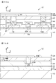
- FIG. 1 is a schematic partial plan view for explaining the configuration of the semiconductor device according to the first embodiment of the present disclosure.
- 2A and 2B are schematic partial cross-sectional views for explaining the configuration of the semiconductor device according to the first embodiment of the present disclosure.
- FIG. 3A is a high-frequency small signal simulation model of the semiconductor device according to the first embodiment of the present disclosure.
- FIG. 3B is a graph showing the relationship between the value of the resistance element and the S parameter obtained by simulation.
- FIG. 4A is a simulation model for investigating the relationship between the internal parameters of the semiconductor device and the resistance element according to the first embodiment of the present disclosure.
- FIG. 4B is a graph showing the relationship between the value of the resistance element and the difference ( ⁇ S12) of the S12 parameter depending on the presence or absence of the resistance element, which is obtained by the simulation.
- FIG. 5 is a graph showing the relationship between the resistance value at which ⁇ S12 is smaller than 1 dB and the internal impedance defined by 1/2 ⁇ C.
- FIG. 6 is a schematic partial plan view for explaining a method of manufacturing a semiconductor device according to the first embodiment of the present disclosure.
- FIG. 7 is a schematic partial plan view for explaining a method of manufacturing a semiconductor device according to the first embodiment of the present disclosure, following FIG.
- FIG. 8 is a schematic partial plan view for explaining a method of manufacturing a semiconductor device according to the first embodiment of the present disclosure, following FIG. 7.
- FIG. 7 is a schematic partial plan view for explaining a method of manufacturing a semiconductor device according to the first embodiment of the present disclosure, following FIG. 7.
- FIG. 7 is a schematic partial plan view for explaining a method of manufacturing
- FIG. 9 is a schematic partial plan view for explaining a method of manufacturing a semiconductor device according to the first embodiment of the present disclosure, following FIG.
- FIG. 10 is a schematic partial plan view for explaining a method of manufacturing a semiconductor device according to the first embodiment of the present disclosure, following FIG. 9.
- FIG. 11 is a schematic partial plan view for explaining a method of manufacturing a semiconductor device according to the first embodiment of the present disclosure, following FIG. 10.
- FIG. 12 is a schematic partial plan view for explaining a method of manufacturing a semiconductor device according to the first embodiment of the present disclosure, following FIG. 11.
- FIG. 13 is a schematic partial plan view for explaining a method of manufacturing a semiconductor device according to the first embodiment of the present disclosure, following FIG. 12.
- FIG. 12 is a schematic partial plan view for explaining a method of manufacturing a semiconductor device according to the first embodiment of the present disclosure, following FIG. 12.
- FIG. 14 is a schematic partial plan view for explaining the configuration of the semiconductor device according to the first modification of the first embodiment of the present disclosure.
- 15A and 15B are schematic partial cross-sectional views for explaining the configuration of the semiconductor device according to the second modification of the first embodiment of the present disclosure.
- 16A and 16B are schematic partial cross-sectional views for explaining the configuration of the semiconductor device according to the third modification of the first embodiment of the present disclosure.
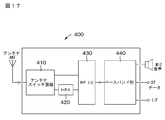
- FIG. 17 is a schematic configuration diagram for explaining a configuration of a wireless communication device using the semiconductor device according to the present disclosure.
- FIG. 18 is a block diagram showing an example of a schematic configuration of a vehicle control system.
- FIG. 19 is an explanatory diagram showing an example of installation positions of the vehicle exterior information detection unit and the image pickup unit.
- the semiconductor device according to the present disclosure the semiconductor device manufactured by the method for manufacturing the semiconductor device according to the present disclosure, and the semiconductor device included in the electronic device according to the present disclosure are simply referred to as [the semiconductor device of the present disclosure. ] May be called.
- the semiconductor device of the present disclosure is Semiconductor material layer forming a channel layer, A pair of source / drain electrodes formed on the semiconductor material layer, and A gate electrode, located between a pair of source / drain electrodes and formed on a semiconductor material layer, Have and At least one of the pair of source / drain electrodes and the gate electrode are connected via a resistance element. It is a semiconductor device.
- the gate electrode can be configured to be formed on the semiconductor material layer via the gate insulating film.
- the semiconductor material layer can be configured to have a barrier layer formed on the channel layer.
- the semiconductor material layer can be composed of a compound semiconductor material, for example, gallium nitride (GaN), gallium arsenide (GaAs), or the like. In some cases, silicon (Si) may be used to form the semiconductor material layer.
- the semiconductor material layer forming the channel layer is located in the channel layer under the gate electrode in a state where no voltage is applied to the pair of source / drain electrodes and the gate electrode.
- the configuration may be such that a dimensional electron gas layer exists.
- the semiconductor device has a normally-on configuration. Therefore, a sufficient effect on PID can be obtained by connecting one of the pair of source / drain electrodes and the gate electrode via a resistance element.
- the semiconductor device has a normally-off configuration, it is preferable that each of the pair of source / drain electrodes is connected to the gate electrode via a resistance element.
- the impedance of the resistance element can be configured to be larger than the internal impedance between the source / drain electrode and the gate electrode to which the resistance element is connected.
- the impedance of the resistance element can be configured to be 1 k ⁇ or more, and more preferably, the impedance of the resistance element is configured to be 1 M ⁇ or more.
- the resistance element can be configured to be arranged in the interlayer film formed on the semiconductor material layer.
- the material constituting the resistance element is not particularly limited.
- it can be configured by using a metal material thinned so that a predetermined resistance value can be obtained, polysilicon, or the like.
- the resistance element may be configured by using a semiconductor material layer formed in the same layer as the semiconductor material layer forming the channel layer.
- a resistance element can be formed by using a semiconductor material layer whose shape is defined by an element separation region.
- the semiconductor material layer is formed on the semiconductor substrate, and the source / drain electrode to which the resistance element is connected and the semiconductor substrate are connected to each other. Can be. According to this configuration, the electric charge charged during the manufacturing process of the semiconductor device can be released to the semiconductor substrate side.
- the material constituting the semiconductor substrate is not particularly limited, and for example, a material such as a III-V compound semiconductor material, silicon carbide (SiC), sapphire, or silicon (Si) can be used.
- a material such as a III-V compound semiconductor material, silicon carbide (SiC), sapphire, or silicon (Si) can be used.
- the method for manufacturing a semiconductor device is as follows. A step of connecting at least one of a pair of source / drain electrodes and a gate electrode via a resistance element, Have.
- Examples of the electronic device provided with the semiconductor device of the present disclosure include a wireless communication device constituting a communication system and the like, and a semiconductor module such as an IC constituting these.
- a wireless communication device a device having a communication frequency of the UHF (Ultra High Frequency) band or higher is particularly effective.
- each drawing used in the following description is a schematic one and does not show an actual size or a ratio thereof.
- FIG. 2 which will be described later, shows the cross-sectional structure of the semiconductor device, but does not show the ratios such as width, height, and thickness.
- the first embodiment relates to a semiconductor device, a method for manufacturing the semiconductor device, and an electronic device according to the present disclosure.
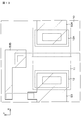
- FIG. 1 is a schematic partial plan view for explaining the configuration of the semiconductor device according to the first embodiment of the present disclosure. More specifically, it shows one of a large number of semiconductor devices formed on a wafer-like substrate. The same applies to other drawings described later.
- the equivalent circuit diagram of the semiconductor device is shown on the right side of FIG.
- the semiconductor device 1 is Semiconductor material layer 11 forming a channel layer, A pair of source / drain electrodes 12, 12A formed on the semiconductor material layer 11 and The gate electrode 31, which is arranged between the pair of source / drain electrodes 12, 12A and is formed on the semiconductor material layer 11. have.
- FIG. 1 the planar shape of the above-mentioned components and the like is represented by hatching.
- the semiconductor device 1 is a field effect transistor having an insulated gate structure.
- the gate electrode 31 is formed on the semiconductor material layer 11 via the gate insulating film, but the gate insulating film is not shown in FIG. 1 for convenience of illustration.
- the gate insulating film will be described in detail later with reference to FIG. 2 described later.
- reference numeral 53 indicates wiring connected to one source / drain electrode 12, and reference numeral 43 indicates a contact connecting them.
- Reference numeral 53A indicates wiring connected to the other source / drain electrode 12A, and reference numeral 43A indicates a contact connecting them.
- Reference numeral 53B indicates wiring connected to the gate electrode 31, and reference numeral 43B indicates a contact connecting them.
- the wirings 53, 53A, and 53B are formed by patterning a conductive material layer formed of the same layer.
- the resistance element 41 (corresponding to the symbol RS in the equivalent circuit diagram) is provided. ) Is connected. More specifically, the resistance element 41 is connected between the wiring 53 connected to one of the source / drain electrodes 12 and the wiring 53B connected to the gate electrode 31.
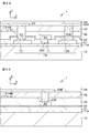
- FIGS. 2A and 2B are schematic partial cross-sectional views for explaining the configuration of the semiconductor device according to the first embodiment of the present disclosure.
- FIG. 2A schematically shows a cross section of a portion of reference numeral A indicated by an alternate long and short dash line in FIG.
- FIG. 2B schematically shows a cross section of a portion of reference numeral B indicated by a chain double-dashed line in FIG.
- the planar shape of each element will be described with reference to FIGS. 6 to 13 for explaining a method for manufacturing a semiconductor device.
- the semiconductor device 1 is formed on the semiconductor substrate 10.
- a semiconductor material layer 11 that forms a channel layer is formed on the semiconductor substrate 10.
- the semiconductor substrate 10 is formed of, for example, a single crystal GaN substrate in relation to the lattice constant with the semiconductor material layer 11 formed on the semiconductor substrate 10.
- the hatched portion shows the planar shape of the semiconductor material layer 11.
- the semiconductor material layer 11 is made of a compound semiconductor material.
- an epitaxial growth layer of gallium nitride (GaN) is used as the semiconductor material layer 11.
- the semiconductor material layer 11 is formed as a u-GaN layer to which impurities are not added.
- a barrier layer (not shown) is formed on the semiconductor material layer 11. Since 2DEG is generated by the polarization generated with the semiconductor material layer 11, Al 1-xy Ga x In y N (provided that 0 ⁇ x ⁇ 1, 0 ⁇ y ⁇ 1) or the like is used as a material for forming the barrier layer. Commonly used.
- the semiconductor material layer 11 forming the channel layer has a two-dimensional electron gas layer in the channel layer under the gate electrode 31 in a state where no voltage is applied to the pair of source / drain electrodes 12, 12A and the gate electrode 31. It is formed.
- a buffer layer may be provided between them. By controlling the lattice constant with the buffer layer, it is possible to improve the crystal state of the semiconductor material layer 11 and control the warp of the wafer-like substrate.
- the semiconductor substrate 1 is made of single crystal silicon, AlN, AlGaN, GaN and the like are used as an example of such a buffer layer.
- the planar shape of the active region of the semiconductor material layer 11 is substantially rectangular. As will be described later, the portion surrounding the active region is designated as an element separation region by injecting boron ions (the portion that has become the element separation region is represented by reference numeral 11A). As shown in FIGS. 1 and 2, a pair of source / drain electrodes 12 and 12A are formed on the semiconductor material layer 11. In FIG. 8, the hatched portion shows the planar shape of the pair of source / drain electrodes 12, 12A.
- the conductive material layer constituting the source / drain electrodes 12, 12A is made of a metal material, for example, a metal such as aluminum (Al), copper (Cu), titanium (Ti), nickel (Ni), gold (Au), or these. It is formed from an alloy or the like whose main component is.
- An annealing treatment may be performed as a means for achieving low resistance.
- a high concentration N + layer may be formed between the semiconductor material layer 11 and the semiconductor material layer 11. After etching the semiconductor material layer 11, it may be formed by selective regrowth in which the high-concentration N + layer is selectively filled, or it may be formed by ion implantation. In the case of selective regrowth, an n-In 1-x Ga x N layer or the like can be used.
- the interlayer insulating layer 21 is formed on the entire surface including the pair of source / drain electrodes 12 and 12A.
- a material having insulating properties with respect to the semiconductor material layer 11 and forming a good interface and not deteriorating the device characteristics is appropriately selected and used.
- the interlayer insulating layer 21 is provided with an opening OP1 in which the semiconductor material layer 11 under the gate electrode 31 is exposed.
- the portion of the semiconductor material layer 11 exposed by the opening OP1 is hatched.
- the insulating film 22 constituting the gate insulating film is formed over the entire surface including the interlayer insulating layer 21 and the opening OP1.
- the insulating film 22 is made of, for example, aluminum oxide (Al 2 O 3 ) or hafnium oxide (HfO 2 ) having a thickness of about 10 nanometers, or a laminate thereof.
- the portion of the insulating film 22 formed in the opening OP1 constitutes the gate insulating film 22A.
- the gate electrode 31 is formed so as to cover the gate insulating film 22A formed in the opening OP1.
- the gate electrode 31 is arranged between the pair of source / drain electrodes 12 and 12A, and is formed on the semiconductor material layer 11 via the gate insulating film 22A.
- the hatched portion shows the planar shape of the gate electrode 31.
- the gate electrode 31 is made of, for example, a material similar to the conductive material constituting the pair of source / drain electrodes 12, 12A.
- an insulating flattening film 32 is formed on the entire surface including the gate electrode 31.
- a resistance element 41 formed by patterning a metal thin film is provided on the flattening film 32.
- An insulating film 42 is formed on the entire surface including the resistance element 41. In this way, the resistance element 41 is arranged in the interlayer film formed on the semiconductor material layer 11.
- the contacts 43 and 43A are formed so as to penetrate the insulating film 42, the flattening film 32, the insulating film 22, and the interlayer insulating layer 21. Further, the contact 43B is formed so as to penetrate the insulating film 42 and the flattening film 32.
- the contacts 43 and 43A are formed so as to be connected to the source / drain electrodes 12 and 12A, respectively. Further, the contact 43B is formed so as to connect with the gate electrode 31.
- contacts 44 and 44B are formed so as to penetrate the insulating film 42.
- the contacts 44 and 44B are formed so as to be connected to the resistance element 41, respectively.
- Wiring 53, 53A, 53B is formed on the insulating film 42.
- the wirings 53, 53A, and 53B are formed by appropriately patterning a conductive material layer formed of the same layer.
- the wirings 53, 53A and 53B are connected to the source / drain electrodes 12, 12A and the gate electrode 31 via the contacts 43, 43A and 43B described above, respectively.
- the wiring 53 is connected to one end of the resistance element 41 via the above-mentioned contact 44, and the wiring 53B is connected to the other end of the resistance element 41 via the above-mentioned contact 44B.
- a protective film 54 is formed on the entire surface including the wirings 53, 53A, and 53B.
- the semiconductor device 1 formed as described above has the same DC potential between the gate and the source and between the gate and the drain during the manufacturing process of the semiconductor device. Therefore, damage to the gate insulating film 22A due to the antenna effect can be prevented.
- the influence on the characteristics of the semiconductor device 1 can be sufficiently reduced by appropriately setting the size of the resistance element 41.
- the impedance of the resistance element may be made larger than the internal impedance between the source / drain electrode and the gate electrode to which the resistance element is connected.
- the impedance of the resistance element 41 may be configured to be 1 k ⁇ or more, and more preferably, the impedance of the resistance element may be configured to be 1 M ⁇ or more.
- FIG. 3A is a high-frequency small signal simulation model of the semiconductor device according to the first embodiment of the present disclosure.
- FIG. 3B is a graph showing the relationship between the value of the resistance element and the S parameter obtained by simulation.
- the transistor TR As the transistor TR, a general HEMT model was used assuming a gate length of about 10 micrometers. Specifically, the source side is connected to the GND, the drain side is terminated by the 50 ⁇ resistor R T2 via the 50 ⁇ load resistor R Lo , and the 50 ⁇ resistor R T1 is arranged between the gate and the GND. It is a circuit that inputs a small signal to the gate. Since a depletion type transistor is used, the resistance element RS is connected only between the gate and the source.
- FIG. 3B shows the result of performing a small signal simulation with the magnitude of the resistance element RS as a parameter.
- the graphs of the S11 to S22 parameters were obtained with the values of the resistance element RS being 1 ⁇ , 10 ⁇ , 100 ⁇ , 1k ⁇ , and 1M ⁇ .
- the graph in the case where the resistance element RS is not provided generally overlaps with the case where the resistance element RS is 1 k ⁇ or 1 M ⁇ .
- the graph of S11 to S22 parameter if the resistance value of the resistance element R S and at least 1k ⁇ above, and when the resistance element R S is a time no, that shows the small signal characteristics of almost the same Shown.
- the S12 when not using the resistive element R S is defined as in S12 difference and ⁇ S12 when using the resistance element R S.
- the relationship between ⁇ S12 and RS is shown in FIG. 4B when the capacitance values are set to 0.1 pF, 0.32 pF, 1 pF, 3.2 pF, and 10 pF, respectively.
- ⁇ S12 is sufficiently close to 0, for example, if the difference is within 1 dB, it can be determined that the influence of the resistance element RS on the characteristics of the semiconductor device 1 is very small.
- FIG. 5 is a graph showing the relationship between the resistance value at which ⁇ S12 is smaller than 1 dB and the internal impedance defined by 1 / 2 ⁇ C.
- ⁇ S12 becomes smaller than 1 dB. Therefore, it can be seen that the influence of connecting the resistance element RS on the characteristics of the semiconductor device 1 is very small. In order to reduce the influence, it is desirable to set the resistance value of the resistance element RS to be one digit or more larger than the internal impedance.
- the resistance value of the resistance element RS is preferably 1 k ⁇ or more, preferably 1 M ⁇ or more.
- the method for manufacturing the semiconductor device 1 includes a step of connecting at least one of the pair of source / drain electrodes and the gate electrode via a resistance element.
- FIGS. 6 to 13 are schematic partial plan views for explaining the configuration of the semiconductor device according to the first embodiment of the present disclosure. From the viewpoint of legibility, the display of the insulating layer and the insulating film is omitted in the plan view in principle.
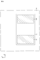
- the semiconductor material layer 11 is formed on the semiconductor substrate 10. Specifically, the semiconductor substrate 10 is prepared, and an epitaxial growth layer of gallium nitride (GaN) is formed as the semiconductor material layer 11 on the entire surface (see FIG. 6). After that, the portion excluding the active region which becomes the channel formation region and the source / drain region is defined as the element separation region 11A. Specifically, boron ions are implanted into the portion to be the device separation region by the ion implantation method to form the device separation region 11A, and a region of the semiconductor material layer 11 surrounded by the device separation region 11A is formed (see FIG. 7). ).
- GaN gallium nitride
- Step-110 (see FIG. 8)
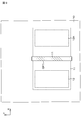
- the source / drain electrodes 12, 12A are formed. Specifically, a conductive material layer made of a metal material is formed on the entire surface including the semiconductor material layer 11. Then, the source / drain electrodes 12, 12A are formed at predetermined positions by a patterning method.
- Step-120 (see FIG. 9) Next, the interlayer insulating layer 21 is formed on the entire surface. After that, an opening OP1 is provided in which the portion of the semiconductor material layer 11 located below the gate electrode 31 is exposed.
- Step-130 (see FIG. 10) Next, the insulating film 22 constituting the gate insulating film 22A and the like is formed on the entire surface. After that, the gate electrode 31 is formed. Specifically, a conductive material layer made of a metal material is formed on the entire surface, and then a gate electrode 31 is formed at a predetermined position by using a well-known patterning method.
- Step-140 (see FIGS. 11 and 12) After that, an insulating flattening film 32 is formed on the entire surface including the gate electrode 31. Next, the resistance element 41 is formed. Specifically, a thin film made of a metal material is formed on the entire surface, and then a resistance element 41 is formed at a predetermined position by using a well-known patterning method (see FIG. 11). After that, the insulating film 42 is formed on the entire surface. Next, openings OP2, OP3, OP4, OP5, OP6 are provided in the portions corresponding to the contacts 43, 43A, 43B, 44, 44B (see FIG. 12).
- Step-150 (see FIG. 13) After that, the openings OP2, OP3, OP4, OP5, OP6 are filled with a conductive material to form a contact, and then the wirings 53, 53A, 53B are formed. Specifically, a conductive material layer made of a metal material is formed on the entire surface, and then wirings 53, 53A, and 53B are formed at predetermined positions by using a well-known patterning method. After that, the protective film 54 is formed on the entire surface.
- the semiconductor device 1 can be manufactured by the above steps.
- the resistance element 41 is arranged in the interlayer film formed on the semiconductor material layer 11.
- the configuration of the resistance element 41 is not limited to this.
- the resistance element 41 can be configured by using a semiconductor material layer formed in the same layer as the semiconductor material layer 11 forming the channel layer.
- the shape of the semiconductor material layer can be defined by the element separation region 11A shown in FIG. 7, and a resistance element having a predetermined resistance value can be formed.
- FIG. 14 is a schematic partial plan view for explaining the configuration of the semiconductor device according to the first modification of the first embodiment of the present disclosure.
- both the source / drain electrode 12 and the gate electrode 31 and the source / drain electrode 12A and the gate electrode 31 are resistance elements. The difference is that they are connected via 41.
- the semiconductor device 1A according to the first modification has a configuration suitable for an enhancement type transistor in which the source and the drain are separated in a state where a bias voltage is not applied to the gate electrode. That is, even if it is an enhancement type transistor, the potential between the gate and the source and the potential between the gate and the drain are DC-equal during the manufacturing process of the semiconductor device. Therefore, damage to the gate insulating film 22A due to the antenna effect can be prevented.
- the semiconductor device 1A differs from the semiconductor device 1 shown in FIG. 1 in that the planar shape of the wiring layer 53 and the like are different, that the resistance elements 41 are provided at two locations, and that the semiconductor device 1A is basically a semiconductor. It has the same configuration as the device 1. Therefore, the description of the semiconductor device 1 may be read as appropriate.
- 15A and 15B are schematic partial cross-sectional views for explaining the configuration of the semiconductor device according to the second modification of the first embodiment of the present disclosure.
- the interlayer insulating layer 21 is provided with an opening OP1 in which the semiconductor material layer 11 under the gate electrode 31 is exposed.
- the opening OP1 is usually formed by dry etching, but at that time, it is considered that the exposed semiconductor material layer 11 is damaged.
- the semiconductor device 1B according to the second modification has a configuration capable of reducing the above-mentioned damage.
- the interlayer insulating layer of the semiconductor material layer 11 has a two-layer structure in which 21 is composed of a lower layer 21A and an upper layer 21B. Then, the upper layer 21B is processed by dry etching and the lower layer 21A is processed by wet etching so that the surface of the semiconductor material layer 11 is not exposed at the time of dry etching, and the damage due to etching is reduced.
- the semiconductor device 1B differs from the semiconductor device 1 shown in FIG. 1 in the above-mentioned points, and basically has the same configuration as the semiconductor device 1. Therefore, the description of the semiconductor device 1 may be read as appropriate.
- 16A and 16B are schematic partial cross-sectional views for explaining the configuration of the semiconductor device according to the third modification of the first embodiment of the present disclosure.
- the semiconductor material layer is formed on the semiconductor substrate, and the source / drain electrode to which the resistance element is connected is connected to the semiconductor substrate.
- the semiconductor device 1C differs from the semiconductor device 1 in that one of the source / drain electrodes 12 is also connected to the semiconductor substrate 10 via the wiring 53 and the contact CT. According to this configuration, the charge accumulated in the gate electrode and the pair of source / drain electrodes can flow to the semiconductor substrate 10 side.
- the semiconductor device 1C has basically the same configuration as the semiconductor device 1 except that the above-mentioned points are different from the semiconductor device 1 shown in FIG. Therefore, the description of the semiconductor device 1 may be read as appropriate.
- the PID in the manufacturing process such as etching using plasma can be reduced, and the process step of removing the wiring before shipping the semiconductor device is not required. Further, the influence on the characteristics of the semiconductor device can be made sufficiently small.
- the semiconductor device of the present disclosure can be used, for example, in an electronic device constituting a wireless communication device in a mobile communication system or the like.
- it is suitable for use as an RF switch or a power amplifier. That is, by using the semiconductor device of the present disclosure having excellent high frequency characteristics and high efficiency characteristics for the RF switch and power amplifier of the wireless communication device, it is possible to achieve high speed, high efficiency and low power consumption of wireless communication. ..
- the usage time can be extended by increasing the speed, efficiency, and power consumption, and the convenience can be further improved.
- FIG. 17 shows an example of an electronic device constituting a wireless communication device.
- the electronic device 400 is a mobile phone system having multiple functions such as voice, data communication, and LAN connection.
- the electronic device 400 includes, for example, an antenna ANT, an antenna switch circuit 410, a high power amplifier (HPA) 420, a high frequency integrated circuit RFIC (Radio Frequency Integrated Circuit) 430, a base band unit 440, and an audio output unit MIC. It has a data output unit DT and an interface unit I / F (for example, wireless LAN (W-LAN; Wireless Local Area Network), Bluetooth (registered trademark), etc.).
- the high-frequency integrated circuit RFIC 430 and the baseband unit 440 are connected by an interface unit I / F.
- the transmission signal output from the baseband unit 440 is a high-frequency integrated circuit RFIC430 and high power. It is output to the antenna ANT via the amplifier (HPA) 420 and the antenna switch circuit 410.
- HPA amplifier
- the received signal is input to the baseband unit 440 via the antenna switch circuit 410 and the high frequency integrated circuit RFIC430.
- the signal processed by the baseband unit 440 is output from an audio output unit MIC, a data output unit DT, and an output unit such as an interface unit I / F.
- the technology according to the present disclosure can be applied to various products.
- the technology according to the present disclosure includes any type of movement such as automobiles, electric vehicles, hybrid electric vehicles, motorcycles, bicycles, personal mobility, airplanes, drones, ships, robots, construction machines, agricultural machines (tractors), and the like. It may be realized as a device mounted on the body.
- FIG. 18 is a block diagram showing a schematic configuration example of a vehicle control system 7000, which is an example of a mobile control system to which the technique according to the present disclosure can be applied.
- the vehicle control system 7000 includes a plurality of electronic control units connected via the communication network 7010.
- the vehicle control system 7000 includes a drive system control unit 7100, a body system control unit 7200, a battery control unit 7300, an external information detection unit 7400, an in-vehicle information detection unit 7500, and an integrated control unit 7600. ..
- the communication network 7010 connecting these plurality of control units conforms to any standard such as CAN (Controller Area Network), LIN (Local Interconnect Network), LAN (Local Area Network) or FlexRay (registered trademark). It may be an in-vehicle communication network.
- CAN Controller Area Network
- LIN Local Interconnect Network
- LAN Local Area Network
- FlexRay registered trademark
- Each control unit includes a microcomputer that performs arithmetic processing according to various programs, a storage unit that stores a program executed by the microcomputer or parameters used for various arithmetics, and a drive circuit that drives various control target devices. To be equipped.
- Each control unit is provided with a network I / F for communicating with other control units via the communication network 7010, and is provided by wired communication or wireless communication with devices or sensors inside or outside the vehicle. A communication I / F for performing communication is provided. In FIG.
- control unit 7600 the microcomputer 7610, the general-purpose communication I / F 7620, the dedicated communication I / F 7630, the positioning unit 7640, the beacon receiving unit 7650, the in-vehicle device I / F 7660, the audio image output unit 7670, The vehicle-mounted network I / F 7680 and the storage unit 7690 are shown.
- Other control units also include a microcomputer, a communication I / F, a storage unit, and the like.
- the drive system control unit 7100 controls the operation of the device related to the drive system of the vehicle according to various programs.
- the drive system control unit 7100 provides a driving force generator for generating the driving force of the vehicle such as an internal combustion engine or a driving motor, a driving force transmission mechanism for transmitting the driving force to the wheels, and a steering angle of the vehicle. It functions as a control device such as a steering mechanism for adjusting and a braking device for generating a braking force of a vehicle.
- the drive system control unit 7100 may have a function as a control device such as ABS (Antilock Brake System) or ESC (Electronic Stability Control).
- the vehicle condition detection unit 7110 is connected to the drive system control unit 7100.
- the vehicle state detection unit 7110 may include, for example, a gyro sensor that detects the angular velocity of the axial rotation motion of the vehicle body, an acceleration sensor that detects the acceleration of the vehicle, an accelerator pedal operation amount, a brake pedal operation amount, or steering wheel steering. Includes at least one of the sensors for detecting angular velocity, engine speed, wheel speed, and the like.
- the drive system control unit 7100 performs arithmetic processing using a signal input from the vehicle state detection unit 7110 to control an internal combustion engine, a drive motor, an electric power steering device, a braking device, and the like.
- the body system control unit 7200 controls the operation of various devices mounted on the vehicle body according to various programs.
- the body system control unit 7200 functions as a keyless entry system, a smart key system, a power window device, or a control device for various lamps such as head lamps, back lamps, brake lamps, blinkers or fog lamps.
- the body system control unit 7200 may be input with radio waves transmitted from a portable device that substitutes for the key or signals of various switches.
- the body system control unit 7200 receives inputs of these radio waves or signals and controls a vehicle door lock device, a power window device, a lamp, and the like.
- the battery control unit 7300 controls the secondary battery 7310, which is the power supply source of the drive motor, according to various programs. For example, information such as the battery temperature, the battery output voltage, or the remaining capacity of the battery is input to the battery control unit 7300 from the battery device including the secondary battery 7310. The battery control unit 7300 performs arithmetic processing using these signals to control the temperature of the secondary battery 7310 or the cooling device provided in the battery device.
- the vehicle outside information detection unit 7400 detects information outside the vehicle equipped with the vehicle control system 7000.
- the image pickup unit 7410 and the vehicle exterior information detection unit 7420 is connected to the vehicle exterior information detection unit 7400.
- the imaging unit 7410 includes at least one of a ToF (Time Of Flight) camera, a stereo camera, a monocular camera, an infrared camera, and other cameras.
- the vehicle exterior information detection unit 7420 is used to detect, for example, the current weather or an environmental sensor for detecting the weather, or other vehicles, obstacles, pedestrians, etc. around the vehicle equipped with the vehicle control system 7000. At least one of the ambient information detection sensors is included.
- the environmental sensor may be, for example, at least one of a raindrop sensor that detects rainy weather, a fog sensor that detects fog, a sunshine sensor that detects the degree of sunshine, and a snow sensor that detects snowfall.
- the ambient information detection sensor may be at least one of an ultrasonic sensor, a radar device, and a LIDAR (Light Detection and Ranging, Laser Imaging Detection and Ranging) device.
- the image pickup unit 7410 and the vehicle exterior information detection unit 7420 may be provided as independent sensors or devices, or may be provided as a device in which a plurality of sensors or devices are integrated.
- FIG. 19 shows an example of the installation positions of the image pickup unit 7410 and the vehicle exterior information detection unit 7420.
- the imaging units 7910, 7912, 7914, 7916, 7918 are provided, for example, at at least one of the front nose, side mirrors, rear bumpers, back door, and upper part of the windshield of the vehicle interior of the vehicle 7900.
- the image pickup unit 7910 provided on the front nose and the image pickup section 7918 provided on the upper part of the windshield in the vehicle interior mainly acquire an image in front of the vehicle 7900.
- the imaging units 7912 and 7914 provided in the side mirrors mainly acquire images of the side of the vehicle 7900.
- the image pickup unit 7916 provided on the rear bumper or the back door mainly acquires an image of the rear of the vehicle 7900.
- the imaging unit 7918 provided on the upper part of the windshield in the vehicle interior is mainly used for detecting a preceding vehicle, a pedestrian, an obstacle, a traffic light, a traffic sign, a lane, or the like.
- FIG. 19 shows an example of the photographing range of each of the imaging units 7910, 7912, 7914, 7916.
- the imaging range a indicates the imaging range of the imaging unit 7910 provided on the front nose
- the imaging ranges b and c indicate the imaging ranges of the imaging units 7912 and 7914 provided on the side mirrors, respectively
- the imaging range d indicates the imaging range d.
- the imaging range of the imaging unit 7916 provided on the rear bumper or the back door is shown. For example, by superimposing the image data captured by the imaging units 7910, 7912, 7914, 7916, a bird's-eye view image of the vehicle 7900 as viewed from above can be obtained.
- the vehicle exterior information detection units 7920, 7922, 7924, 7926, 7928, 7930 provided on the front, rear, side, corners and the upper part of the windshield in the vehicle interior of the vehicle 7900 may be, for example, an ultrasonic sensor or a radar device.
- the vehicle exterior information detection units 7920, 7926, 7930 provided on the front nose, rear bumper, back door, and upper part of the windshield in the vehicle interior of the vehicle 7900 may be, for example, a lidar device.
- These out-of-vehicle information detection units 7920 to 7930 are mainly used for detecting a preceding vehicle, a pedestrian, an obstacle, or the like.
- the vehicle outside information detection unit 7400 causes the image pickup unit 7410 to capture an image of the outside of the vehicle and receives the captured image data. Further, the vehicle exterior information detection unit 7400 receives detection information from the connected vehicle exterior information detection unit 7420. When the vehicle exterior information detection unit 7420 is an ultrasonic sensor, a radar device, or a lidar device, the vehicle exterior information detection unit 7400 transmits ultrasonic waves, electromagnetic waves, or the like, and receives the received reflected wave information.
- the vehicle exterior information detection unit 7400 may perform object detection processing or distance detection processing such as a person, a vehicle, an obstacle, a sign, or a character on a road surface based on the received information.
- the vehicle exterior information detection unit 7400 may perform an environment recognition process for recognizing rainfall, fog, road surface conditions, etc., based on the received information.
- the vehicle outside information detection unit 7400 may calculate the distance to an object outside the vehicle based on the received information.
- the vehicle exterior information detection unit 7400 may perform image recognition processing or distance detection processing for recognizing a person, a vehicle, an obstacle, a sign, a character on the road surface, or the like based on the received image data.
- the vehicle exterior information detection unit 7400 performs processing such as distortion correction or alignment on the received image data, and synthesizes the image data captured by different imaging units 7410 to generate a bird's-eye view image or a panoramic image. May be good.
- the vehicle exterior information detection unit 7400 may perform the viewpoint conversion process using the image data captured by different imaging units 7410.
- the in-vehicle information detection unit 7500 detects the in-vehicle information.
- a driver state detection unit 7510 that detects the driver's state is connected to the in-vehicle information detection unit 7500.
- the driver state detection unit 7510 may include a camera that captures the driver, a biosensor that detects the driver's biological information, a microphone that collects sound in the vehicle interior, and the like.
- the biosensor is provided on, for example, the seat surface or the steering wheel, and detects the biometric information of the passenger sitting on the seat or the driver holding the steering wheel.
- the in-vehicle information detection unit 7500 may calculate the degree of fatigue or concentration of the driver based on the detection information input from the driver state detection unit 7510, and may determine whether the driver is dozing or not. You may.
- the in-vehicle information detection unit 7500 may perform processing such as noise canceling processing on the collected audio signal.
- the integrated control unit 7600 controls the overall operation in the vehicle control system 7000 according to various programs.
- An input unit 7800 is connected to the integrated control unit 7600.
- the input unit 7800 is realized by a device such as a touch panel, a button, a microphone, a switch or a lever, which can be input-operated by a passenger. Data obtained by recognizing the voice input by the microphone may be input to the integrated control unit 7600.
- the input unit 7800 may be, for example, a remote control device using infrared rays or other radio waves, or an externally connected device such as a mobile phone or a PDA (Personal Digital Assistant) that supports the operation of the vehicle control system 7000. You may.
- the input unit 7800 may be, for example, a camera, in which case the passenger can input information by gesture. Alternatively, data obtained by detecting the movement of the wearable device worn by the passenger may be input. Further, the input unit 7800 may include, for example, an input control circuit that generates an input signal based on the information input by the passenger or the like using the input unit 7800 and outputs the input signal to the integrated control unit 7600. By operating the input unit 7800, the passenger or the like inputs various data to the vehicle control system 7000 and instructs the processing operation.
- the storage unit 7690 may include a ROM (Read Only Memory) for storing various programs executed by the microcomputer, and a RAM (Random Access Memory) for storing various parameters, calculation results, sensor values, and the like. Further, the storage unit 7690 may be realized by a magnetic storage device such as an HDD (Hard Disc Drive), a semiconductor storage device, an optical storage device, an optical magnetic storage device, or the like.
- ROM Read Only Memory
- RAM Random Access Memory
- the general-purpose communication I / F 7620 is a general-purpose communication I / F that mediates communication with various devices existing in the external environment 7750.
- General-purpose communication I / F7620 is a cellular communication protocol such as GSM (registered trademark) (Global System of Mobile communications), WiMAX, LTE (Long Term Evolution) or LTE-A (LTE-Advanced), or wireless LAN (Wi-Fi).
- GSM Global System of Mobile communications
- WiMAX Wireless F
- LTE Long Term Evolution
- LTE-A Long Term Evolution-A
- Wi-Fi wireless LAN
- Other wireless communication protocols such as (also referred to as (registered trademark)) and Bluetooth (registered trademark) may be implemented.
- the general-purpose communication I / F 7620 connects to a device (for example, an application server or a control server) existing on an external network (for example, the Internet, a cloud network, or a business-specific network) via, for example, a base station or an access point. You may. Further, the general-purpose communication I / F7620 uses, for example, P2P (Peer To Peer) technology, and is a terminal existing in the vicinity of the vehicle (for example, a terminal of a driver, a pedestrian, or a store, or an MTC (Machine Type Communication) terminal). May be connected with.
- P2P Peer To Peer
- MTC Machine Type Communication
- the dedicated communication I / F 7630 is a communication I / F that supports a communication protocol formulated for use in a vehicle.
- the dedicated communication I / F7630 uses a standard protocol such as WAVE (Wireless Access in Vehicle Environment), DSRC (Dedicated Short Range Communications), or cellular communication protocol, which is a combination of lower layer IEEE802.11p and upper layer IEEE1609. May be implemented.
- Dedicated communication I / F7630 typically includes vehicle-to-vehicle (Vehicle to Vehicle) communication, road-to-vehicle (Vehicle to Infrastructure) communication, vehicle-to-home (Vehicle to Home) communication, and pedestrian-to-pedestrian (Vehicle to Pedestrian) communication. ) Carry out V2X communication, a concept that includes one or more of the communications.
- the positioning unit 7640 receives, for example, a GNSS signal from a GNSS (Global Navigation Satellite System) satellite (for example, a GPS signal from a GPS (Global Positioning System) satellite), executes positioning, and executes positioning, and the latitude, longitude, and altitude of the vehicle. Generate location information including.
- the positioning unit 7640 may specify the current position by exchanging signals with the wireless access point, or may acquire position information from a terminal such as a mobile phone, PHS, or smartphone having a positioning function.
- the beacon receiving unit 7650 receives radio waves or electromagnetic waves transmitted from a radio station or the like installed on the road, and acquires information such as the current position, traffic jam, road closure, or required time.
- the function of the beacon receiving unit 7650 may be included in the above-mentioned dedicated communication I / F 7630.
- the in-vehicle device I / F 7660 is a communication interface that mediates the connection between the microcomputer 7610 and various in-vehicle devices 7760 existing in the vehicle.
- the in-vehicle device I / F7660 may establish a wireless connection using a wireless communication protocol such as wireless LAN, Bluetooth (registered trademark), NFC (Near Field Communication) or WUSB (Wireless USB).
- a wireless communication protocol such as wireless LAN, Bluetooth (registered trademark), NFC (Near Field Communication) or WUSB (Wireless USB).
- the in-vehicle device I / F7660 is via a connection terminal (and a cable if necessary) (not shown), USB (Universal Serial Bus), HDMI (registered trademark) (High-Definition Multimedia Interface), or MHL (Mobile).
- a wired connection such as High-definition Link may be established.
- the in-vehicle device 7760 may include, for example, at least one of a passenger's mobile device or wearable device, or an information device carried or attached to the vehicle.
- the in-vehicle device 7760 may include a navigation device that searches for a route to an arbitrary destination.
- the in-vehicle device I / F 7660 exchanges control signals or data signals with these in-vehicle devices 7760.
- the in-vehicle network I / F7680 is an interface that mediates communication between the microcomputer 7610 and the communication network 7010.
- the vehicle-mounted network I / F7680 transmits and receives signals and the like according to a predetermined protocol supported by the communication network 7010.
- the microcomputer 7610 of the integrated control unit 7600 is via at least one of general-purpose communication I / F7620, dedicated communication I / F7630, positioning unit 7640, beacon receiving unit 7650, in-vehicle device I / F7660, and in-vehicle network I / F7680. Based on the information acquired in the above, the vehicle control system 7000 is controlled according to various programs. For example, the microcomputer 7610 calculates the control target value of the driving force generator, the steering mechanism, or the braking device based on the acquired information inside and outside the vehicle, and outputs a control command to the drive system control unit 7100. May be good.
- the microcomputer 7610 realizes ADAS (Advanced Driver Assistance System) functions including vehicle collision avoidance or impact mitigation, follow-up driving based on inter-vehicle distance, vehicle speed maintenance driving, vehicle collision warning, vehicle lane deviation warning, and the like. Cooperative control may be performed for the purpose of.
- the microcomputer 7610 automatically travels autonomously without relying on the driver's operation by controlling the driving force generator, steering mechanism, braking device, etc. based on the acquired information on the surroundings of the vehicle. Coordinated control for the purpose of driving or the like may be performed.
- ADAS Advanced Driver Assistance System
- the microcomputer 7610 has information acquired via at least one of general-purpose communication I / F7620, dedicated communication I / F7630, positioning unit 7640, beacon receiving unit 7650, in-vehicle device I / F7660, and in-vehicle network I / F7680. Based on the above, three-dimensional distance information between the vehicle and an object such as a surrounding structure or a person may be generated, and local map information including the peripheral information of the current position of the vehicle may be created. Further, the microcomputer 7610 may predict a danger such as a vehicle collision, a pedestrian or the like approaching or entering a closed road based on the acquired information, and may generate a warning signal.
- the warning signal may be, for example, a signal for generating a warning sound or turning on a warning lamp.
- the audio image output unit 7670 transmits an output signal of at least one of audio and image to an output device capable of visually or audibly notifying information to the passengers of the vehicle or outside the vehicle.
- an audio speaker 7710, a display unit 7720, and an instrument panel 7730 are exemplified as output devices.
- the display unit 7720 may include, for example, at least one of an onboard display and a heads-up display.
- the display unit 7720 may have an AR (Augmented Reality) display function.
- the output device may be other devices other than these devices, such as headphones, wearable devices such as eyeglass-type displays worn by passengers, and projectors or lamps.
- the display device displays the results obtained by various processes performed by the microcomputer 7610 or the information received from other control units in various formats such as texts, images, tables, and graphs. Display visually.
- the audio output device converts an audio signal composed of reproduced audio data, acoustic data, or the like into an analog signal and outputs the audio signal audibly.
- At least two control units connected via the communication network 7010 may be integrated as one control unit.
- each control unit may be composed of a plurality of control units.
- the vehicle control system 7000 may include another control unit (not shown).
- the other control unit may have a part or all of the functions carried out by any of the control units. That is, as long as information is transmitted and received via the communication network 7010, predetermined arithmetic processing may be performed by any control unit.
- a sensor or device connected to one of the control units may be connected to the other control unit, and the plurality of control units may send and receive detection information to and from each other via the communication network 7010. .
- the technology according to the present disclosure can be applied to, for example, various devices that control communication among the configurations described above.
- the technology of the present disclosure can also have the following configurations.
- [A1] Semiconductor material layer forming a channel layer, A pair of source / drain electrodes formed on the semiconductor material layer, and A gate electrode, located between a pair of source / drain electrodes and formed on a semiconductor material layer, Have and At least one of the pair of source / drain electrodes and the gate electrode are connected via a resistance element.
- the gate electrode is formed on the semiconductor material layer via the gate insulating film.
- [A3] The semiconductor material layer has a barrier layer formed on the channel layer.
- [A4] The semiconductor material layer is made of compound semiconductor material, The semiconductor device according to the above [A3].
- the semiconductor material layer forming the channel layer is formed so that a two-dimensional electron gas layer exists in the channel layer under the gate electrode when no voltage is applied to the pair of source / drain electrodes and the gate electrode.
- the impedance of the resistance element is greater than the internal impedance between the source / drain electrode and the gate electrode to which the resistance element is connected.
- the impedance of the resistance element is 1 k ⁇ or more.
- [A8] The impedance of the resistance element is 1 M ⁇ or more.
- the resistance element is arranged in the interlayer film formed on the semiconductor material layer.
- the resistance element is configured by using a semiconductor material layer formed in the same layer as the semiconductor material layer forming the channel layer.
- the semiconductor material layer is formed on the semiconductor substrate and The source / drain electrode to which the resistance element is connected and the semiconductor substrate are connected, The semiconductor device according to any one of the above [A1] to [A10].
- [B1] Semiconductor material layer forming a channel layer, A pair of source / drain electrodes formed on the semiconductor material layer, and A gate electrode, located between a pair of source / drain electrodes and formed on a semiconductor material layer, Have and At least one of the pair of source / drain electrodes and the gate electrode are connected via a resistance element.
- the gate electrode is formed on the semiconductor material layer via the gate insulating film.
- the semiconductor material layer has a barrier layer formed on the channel layer.
- the semiconductor material layer is made of compound semiconductor material, The electronic device according to the above [B3].
- the semiconductor material layer forming the channel layer is formed so that a two-dimensional electron gas layer exists in the channel layer under the gate electrode when no voltage is applied to the pair of source / drain electrodes and the gate electrode.
- the impedance of the resistance element is greater than the internal impedance between the source / drain electrode and the gate electrode to which the resistance element is connected.
- the impedance of the resistance element is 1 k ⁇ or more.
- the impedance of the resistance element is 1 M ⁇ or more.
- the resistance element is arranged in the interlayer film formed on the semiconductor material layer.
- the resistance element is configured by using a semiconductor material layer formed in the same layer as the semiconductor material layer forming the channel layer.
- the semiconductor material layer is formed on the semiconductor substrate and The source / drain electrode to which the resistance element is connected and the semiconductor substrate are connected, The electronic device according to any one of the above [B1] to [B10].
- Antenna switch circuit 420 ... High power amplifier (HPA), 430 ... High frequency integrated circuit RFIC, 440 ... Base band portion, OP1 ... openings provided in the interlayer insulating layer, OP2, OP3, OP4 ... openings provided in the flattening film, OP5, OP6 ... openings provided in the insulating film, TR ... ⁇ ⁇ Part of electric field effect type transistor with insulating gate structure, RS ⁇ ⁇ ⁇ Resistance element
Landscapes
- Junction Field-Effect Transistors (AREA)
- Metal-Oxide And Bipolar Metal-Oxide Semiconductor Integrated Circuits (AREA)
- Thin Film Transistor (AREA)
- Insulated Gate Type Field-Effect Transistor (AREA)
- Semiconductor Integrated Circuits (AREA)
Abstract
半導体装置は、チャネル層を形成する半導体材料層、半導体材料層上に形成された一対のソース/ドレイン電極、及び、一対のソース/ドレイン電極の間に配置されており、半導体材料層の上に形成されているゲート電極、を有しており、一対のソース/ドレイン電極の少なくとも一方とゲート電極との間は、抵抗素子を介して接続されている。
Description
本開示は、半導体装置および電子機器に関する。
ワイドギャップ半導体材料である窒化ガリウム(GaN)は、絶縁破壊電圧が高く、高温動作が可能であり、飽和ドリフト速度が高いなどといった特徴を有している。また、GaN系ヘテロ接合に形成される二次元電子ガス(2DEG)は、移動度が高くかつシート電子密度が高いという特徴がある。これらの特徴により、GaN系ヘテロFETは低抵抗、高速、高耐圧動作が可能であるため、パワーデバイスやRFデバイスなどへの適用が期待されている。
一般的なGaN系ヘテロFET(HFET)の場合、チャネル層を形成するGaN層の上にバリア層が配される。チャネル層との間で発生する分極によって2DEGを発生させるため、バリア層を形成する材料としてAl1-x-yGaxInyN(但し0≦x<1,0≦y<1)などが一般的に用いられる。良好な特性を実現できるように組成は適宜選択されるが、組成によっては、ゲート電極とバリア層との間に形成されるショットキー接合におけるリーク電流が高くなることが一般的に知られている。その場合、ゲート絶縁膜を介してゲート電極を配置することによって、リーク電流を低減させることができる。
半導体装置の製造プロセスでは、プラズマを用いたエッチングなどの製造工程において、導体層配線にチャージされた電荷によってダメージを受けるPID(Plasma Induced Damage)と言われる現象が発生する。このため、低耐圧のキャパシタをゲート電極に接続し、低耐圧のキャパシタが絶縁破壊することによってチャージされた電荷を逃がすといったことが提案されている(例えば、特許文献1を参照)。
低耐圧のキャパシタが絶縁破壊することによってチャージされた電荷を逃がすといった半導体装置においては、半導体装置の出荷前にキャパシタを接続する配線を除去するなどといったこと必要となる。しかしながら、この場合には配線を除去するプロセス工程などが必要となるためコスト上昇の要因となる。
従って、本開示の目的は、プラズマを用いたエッチングなどの製造工程におけるPIDを低減することができ、半導体装置の出荷前に配線を除去するプロセス工程を必要としない半導体装置、及び、係る半導体装置を備えた電子機器を有することにある。
上記の目的を達成するための本発明に係る半導体装置は、
チャネル層を形成する半導体材料層、
半導体材料層上に形成された一対のソース/ドレイン電極、及び、
一対のソース/ドレイン電極の間に配置されており、半導体材料層の上に形成されているゲート電極、
を有しており、
一対のソース/ドレイン電極の少なくとも一方とゲート電極との間は、抵抗素子を介して接続されている、
半導体装置である。
チャネル層を形成する半導体材料層、
半導体材料層上に形成された一対のソース/ドレイン電極、及び、
一対のソース/ドレイン電極の間に配置されており、半導体材料層の上に形成されているゲート電極、
を有しており、
一対のソース/ドレイン電極の少なくとも一方とゲート電極との間は、抵抗素子を介して接続されている、
半導体装置である。
上記の目的を達成するための本発明に係る電子機器は、
チャネル層を形成する半導体材料層、
半導体材料層上に形成された一対のソース/ドレイン電極、及び、
一対のソース/ドレイン電極の間に配置されており、半導体材料層の上に形成されているゲート電極、
を有しており、
一対のソース/ドレイン電極の少なくとも一方とゲート電極との間は、抵抗素子を介して接続されている、
半導体装置を備えた電子機器である。
チャネル層を形成する半導体材料層、
半導体材料層上に形成された一対のソース/ドレイン電極、及び、
一対のソース/ドレイン電極の間に配置されており、半導体材料層の上に形成されているゲート電極、
を有しており、
一対のソース/ドレイン電極の少なくとも一方とゲート電極との間は、抵抗素子を介して接続されている、
半導体装置を備えた電子機器である。
以下、図面を参照して、実施形態に基づいて本開示を説明する。本開示は実施形態に限定されるものではなく、実施形態における種々の数値や材料は例示である。以下の説明において、同一要素または同一機能を有する要素には同一符号を用いることとし、重複する説明は省略する。尚、説明は、以下の順序で行う。
1.本開示に係る、半導体装置および半導体装置の製造方法、並びに電子機器、全般に関する説明
2.第1の実施形態
3.第1変形例
4.第2変形例
5.第3変形例
6.電子機器の説明
7.応用例
8.その他
1.本開示に係る、半導体装置および半導体装置の製造方法、並びに電子機器、全般に関する説明
2.第1の実施形態
3.第1変形例
4.第2変形例
5.第3変形例
6.電子機器の説明
7.応用例
8.その他
[本開示に係る、半導体装置および半導体装置の製造方法、並びに電子機器、全般に関する説明]
以下の説明において、本開示に係る半導体装置、本開示に係る半導体装置の製造方法によって製造される半導体装置、及び、本開示に係る電子機器が備える半導体装置を、単に、[本開示の半導体装置]と呼ぶ場合がある。
以下の説明において、本開示に係る半導体装置、本開示に係る半導体装置の製造方法によって製造される半導体装置、及び、本開示に係る電子機器が備える半導体装置を、単に、[本開示の半導体装置]と呼ぶ場合がある。
上述したように、本開示の半導体装置は、
チャネル層を形成する半導体材料層、
半導体材料層上に形成された一対のソース/ドレイン電極、及び、
一対のソース/ドレイン電極の間に配置されており、半導体材料層の上に形成されているゲート電極、
を有しており、
一対のソース/ドレイン電極の少なくとも一方とゲート電極との間は、抵抗素子を介して接続されている、
半導体装置である。
チャネル層を形成する半導体材料層、
半導体材料層上に形成された一対のソース/ドレイン電極、及び、
一対のソース/ドレイン電極の間に配置されており、半導体材料層の上に形成されているゲート電極、
を有しており、
一対のソース/ドレイン電極の少なくとも一方とゲート電極との間は、抵抗素子を介して接続されている、
半導体装置である。
そして、本開示の半導体装置において、ゲート電極は、ゲート絶縁膜を介して半導体材料層上に形成されている構成とすることができる。この場合において、半導体材料層は、チャネル層上に形成されたバリア層を有する構成とすることができる。また、半導体材料層は化合物半導体材料から成る構成とすることができ、例えば、窒化ガリウム(GaN)やガリウム砒素(GaAs)などから構成することができる。尚、場合によっては、シリコン(Si)を用いて半導体材料層を形成する構成であってもよい。
上述した各種の好ましい構成を含む本開示の半導体装置において、チャネル層を形成する半導体材料層は、一対のソース/ドレイン電極およびゲート電極に電圧を印加しない状態においてゲート電極下のチャネル層内に2次元電子ガス層が存在するように形成されている構成とすることができる。
この場合、半導体装置はノーマリーオンの構成となる。従って、一対のソース/ドレイン電極のいずれか一方とゲート電極との間が抵抗素子を介して接続されることによって、PIDに対する充分な効果を得ることができる。尚、半導体装置がノーマリーオフの構成である場合には、一対のソース/ドレイン電極のいずれも、ゲート電極との間が抵抗素子を介して接続される構成とすることが好ましい。
上述した各種の好ましい構成を含む本開示の半導体装置において、抵抗素子のインピーダンスは、抵抗素子が接続されるソース/ドレイン電極とゲート電極との間の内部インピーダンスよりも大きい構成とすることができる。この場合において、抵抗素子のインピーダンスは1kΩ以上である構成とすることができるし、より好ましくは、抵抗素子のインピーダンスは1MΩ以上である構成とすることが望ましい。
上述した各種の好ましい構成を含む本開示の半導体装置において、抵抗素子は半導体材料層上に形成された層間膜内に配置されている構成とすることができる。この場合において、抵抗素子を構成する材料は特に限定するものではない。例えば、所定の抵抗値が得られるように薄膜化された金属材料や、ポリシリコンなどを用いて構成することができる。
あるいは又、この場合において、抵抗素子はチャネル層を形成する半導体材料層と同層で形成された半導体材料層を用いて構成されている態様とすることもできる。例えば、素子分離領域によって形状を規定した半導体材料層を用いて抵抗素子を形成することができる。
上述した各種の好ましい構成を含む本開示の半導体装置において、半導体材料層は半導体基板の上に形成されており、抵抗素子が接続されているソース/ドレイン電極と半導体基板とは接続されている構成とすることができる。この構成によれば、半導体装置の製造プロセス中にチャージした電荷を半導体基板側に逃がすことができる。
半導体基板を構成する材料は特に限定するものではなく、例えばIII-V族化合物半導体材料、炭化ケイ素(SiC)、サファイヤ、シリコン(Si)などといった材料を用いることができる。尚、半導体基板と、その上に形成される半導体材料層とで格子定数が異なる場合、それらの間にバッファ層を設けることによって格子定数の相違による影響を低減することができる。
本開示に係る半導体装置の製造方法は、
一対のソース/ドレイン電極の少なくとも一方とゲート電極との間を、抵抗素子を介して接続する工程、
を有する。
一対のソース/ドレイン電極の少なくとも一方とゲート電極との間を、抵抗素子を介して接続する工程、
を有する。
本開示の半導体装置を備えた電子機器として、例えば、通信システムなどを構成する無線通信装置や、これらを構成するICなどの半導体モジュールなどを挙げることができる。このような無線通信装置としては、通信周波数がUHF(Ultra High Frequency)帯以上のもので特に効果が発揮される。
本明細書における各種の条件は、数学的に厳密に成立する場合の他、実質的に成立する場合にも満たされる。設計上あるいは製造上生ずる種々のばらつきの存在は許容される。また、以下の説明で用いる各図面は模式的なものであり、実際の寸法やその割合を示すものではない。例えば、後述する図2は半導体装置の断面構造を示すが、幅、高さ、厚さなどの割合を示すものではない。
[第1の実施形態]
第1の実施形態は、本開示に係る、半導体装置および半導体装置の製造方法、並びに電子機器に関する。
第1の実施形態は、本開示に係る、半導体装置および半導体装置の製造方法、並びに電子機器に関する。
図1は、本開示の第1の実施形態に係る半導体装置の構成を説明するための模式的な一部平面図である。より具体的には、ウエハ状基板に形成される多数の半導体装置のうちの1つを示す。後述する他の図面においても同様である。尚、図1の右側には、半導体装置の等価回路図を示す。
第1の実施形態に係る半導体装置1は、
チャネル層を形成する半導体材料層11、
半導体材料層11上に形成された一対のソース/ドレイン電極12,12A、及び、
一対のソース/ドレイン電極12,12Aの間に配置されており、半導体材料層11の上に形成されているゲート電極31、
を有している。尚、図1において、上述した構成要素などの平面形状をハッチングで表した。
チャネル層を形成する半導体材料層11、
半導体材料層11上に形成された一対のソース/ドレイン電極12,12A、及び、
一対のソース/ドレイン電極12,12Aの間に配置されており、半導体材料層11の上に形成されているゲート電極31、
を有している。尚、図1において、上述した構成要素などの平面形状をハッチングで表した。
半導体装置1は、絶縁ゲート構造を持つ電界効果型トランジスタである。ゲート電極31は、ゲート絶縁膜を介して半導体材料層11上に形成されているが、図示の都合上、図1においてゲート絶縁膜は示されていない。ゲート絶縁膜については、後述する図2を参照して後で詳しく説明する。
図1において、符号53は一方のソース/ドレイン電極12に接続される配線を示し、符号43はそれらを接続するコンタクトを示す。符号53Aは他方のソース/ドレイン電極12Aに接続される配線を示し、符号43Aはそれらを接続するコンタクトを示す。符号53Bは、ゲート電極31に接続される配線を示し、符号43Bはそれらを接続するコンタクトを示す。配線53,53A,53Bは、同層で形成された導電材料層をパターニングすることで形成されている。
そして、一対のソース/ドレイン電極12,12Aの少なくとも一方(図に示す例では、ソース/ドレイン電極12)とゲート電極31との間は、抵抗素子41(等価回路図における符号RSに対応する)を介して接続されている。より具体的には、一方のソース/ドレイン電極12に接続する配線53と、ゲート電極31に接続する配線53Bとの間には、抵抗素子41が接続されている。
図2Aおよび図2Bは、本開示の第1の実施形態に係る半導体装置の構成を説明するための模式的な一部断面図である。図2Aは、図1において一点鎖線で示す符号Aの部分の断面を模式的に示す。図2Bは、図1において一点鎖線で示す符号Bの部分の断面を模式的に示す。尚、各要素の平面形状については、半導体装置の製造方法を説明するための図6ないし図13を適宜参照して説明する。
半導体装置1は、半導体基板10の上に形成されている。半導体基板10上には、チャネル層を形成する半導体材料層11が形成されている。半導体基板10は、その上に形成される半導体材料層11との格子定数との関係から、例えば単結晶GaN基板から形成されている。図7においてハッチングを付した部分が半導体材料層11の平面形状を示す。
半導体材料層11は化合物半導体材料から成る。例えば、半導体材料層11として、窒化ガリウム(GaN)のエピタキシャル成長層が用いられる。半導体材料層11は、不純物を添加しないu-GaN層として形成されている。半導体材料層11の上には、図示せぬバリア層が形成されている。半導体材料層11との間で発生する分極によって2DEGを発生させるため、バリア層を形成する材料としてAl1-x-yGaxInyN(但し0≦x<1,0≦y<1)などが一般的に用いられる。チャネル層を形成する半導体材料層11は、一対のソース/ドレイン電極12,12Aおよびゲート電極31に電圧を印加しない状態においてゲート電極31下のチャネル層内に2次元電子ガス層が存在するように形成されている。
尚、半導体基板10を構成する材料と半導体材料層11を構成する材料との格子定数が相違する場合には、これらの間にバッファ層を設ければよい。バッファ層によって格子定数を制御する事で、半導体材料層11の結晶状態を良好にするとともに、ウエハ状基板の反りを制御することができる。例えば、半導体基板1が単結晶シリコンから成る場合、このようなバッファ層の一例として、AlN、AlGaN、GaNなどが用いられる。
図7に示すように、半導体材料層11のアクティブ領域の平面形状は略矩形である。後述するように、アクティブ領域を囲む部分はボロンイオンの注入によって素子分離領域とされている(素子分離領域となった部分を符号11Aで表す)。図1及び図2に示すように、半導体材料層11上には、一対のソース/ドレイン電極12,12Aが形成されている。図8においてハッチングを付した部分が一対のソース/ドレイン電極12,12Aの平面形状を示す。ソース/ドレイン電極12,12Aを構成する導電材料層は金属材料から成り、例えば、アルミニウム(Al)、銅(Cu)、チタン(Ti)、ニッケル(Ni)、金(Au)等の金属あるいはこれらを主成分とする合金等から形成されている。
尚、低抵抗を実現する手段としてアニール処理を施してもよい。また、更なる低抵抗化を図るため、半導体材料層11との間に高濃度N+層が形成されていてもよい。半導体材料層11のエッチング後に高濃度N+層を選択的に埋める選択再成長により形成してもよいし、イオン注入により形成しても良い。選択再成長の場合は、n-In1-xGaxN層などを用いることができる。
図2Aおよび図2Bに示すように、一対のソース/ドレイン電極12,12A上を含む全面に、層間絶縁層21が形成されている。層間絶縁層21を構成する材料として、半導体材料層11に対して絶縁性を有しかつ良好な界面を形成してデバイス特性を劣化させないような材料が適宜選択して用いられる。
図9に示すように、層間絶縁層21には、ゲート電極31の下の半導体材料層11が露出する開口OP1が設けられている。図9においては、開口OP1によって露出する半導体材料層11の部分にハッチングを付した。
図2Aおよび図2Bに示すように、ゲート絶縁膜を構成する絶縁膜22は、層間絶縁層21や開口OP1上を含む全面に亘って形成されている。絶縁膜22は、例えば厚さが10ナノメートル程度のアルミニウム酸化物(Al2O3)やハフニウム酸化物(HfO2)、あるいはその積層などによって構成されている。開口OP1内に形成された絶縁膜22の部分がゲート絶縁膜22Aを構成する。
そして、開口OP1内に形成されたゲート絶縁膜22Aを覆うように、ゲート電極31が形成されている。図1に示すように、ゲート電極31は、一対のソース/ドレイン電極12,12Aの間に配置されており、ゲート絶縁膜22Aを介して半導体材料層11上に形成されている。図10においてハッチングを付した部分がゲート電極31の平面形状を示す。ゲート電極31は例えば一対のソース/ドレイン電極12,12Aを構成する導電材料と同様の材料を用いて構成されている。
図2Aおよび図2Bに示すように、ゲート電極31上を含む全面には、絶縁性の平坦化膜32が形成されている。平坦化膜32上には、例えば金属薄膜がパターニングされて成る抵抗素子41が設けられている。抵抗素子41上を含む全面には、絶縁膜42が形成されている。このように、抵抗素子41は半導体材料層11上に形成された層間膜内に配置されている。
そして、絶縁膜42、平坦化膜32、絶縁膜22および層間絶縁層21を貫くように、コンタクト43,43Aが形成されている。また、絶縁膜42および平坦化膜32を貫くように、コンタクト43Bが形成されている。コンタクト43,43Aは、それぞれ、ソース/ドレイン電極12,12Aと接続するように形成されている。また、コンタクト43Bは、ゲート電極31と接続するように形成されている。
また、絶縁膜42を貫くように、コンタクト44,44Bが形成されている。コンタクト44,44Bは、それぞれ、抵抗素子41と接続するように形成されている。
絶縁膜42上には、配線53,53A,53Bが形成されている。配線53,53A,53Bは、同層で形成された導電材料層を適宜パターニング等して形成されている。配線53,53A,53Bはそれぞれ、上述したコンタクト43,43A,43Bを介して、ソース/ドレイン電極12,12A、ゲート電極31に接続されている。
また、配線53は上述したコンタクト44を介して抵抗素子41の一端に接続されており、配線53Bは上述したコンタクト44Bを介して抵抗素子41の他端に接続されている。配線53,53A,53B上を含む全面には保護膜54が形成されている。
以上のようにして形成された半導体装置1は、半導体装置の製造プロセス中に、ゲート-ソース間およびゲート-ドレイン間がDC的に同電位となる。したがって、アンテナ効果によるゲート絶縁膜22Aへのダメージを防ぐことが出来る。
一方、半導体装置1の特性への影響は、抵抗素子41の大きさを適切に設定する事で、充分に小さくすることができる。具体的には、抵抗素子のインピーダンスを、抵抗素子が接続されるソース/ドレイン電極とゲート電極との間の内部インピーダンスよりも大きくすればよい。抵抗素子41のインピーダンスは1kΩ以上である構成とすることができるし、より好ましくは、抵抗素子のインピーダンスは1MΩ以上である構成とすればよい。
図3Aは、本開示の第1の実施形態に係る半導体装置の高周波小信号シミュレーション用モデルである。図3Bは、シミュレーションによって得られた、抵抗素子の値とSパラメータとの関係を示すグラフである。
半導体装置1の特性への影響を調べるため、図3Aに示すモデルを用いて高周波小信号シミュレーションを実施した。なお、この回路はゲート電極への入力信号を増幅するいわゆるパワーアンプを想定している。
トランジスタTRとして、ゲート長10マイクロメートル程度を想定し、一般的なHEMTモデルを使用した。具体的には、ソース側がGNDに接続され、ドレイン側は50Ωの負荷抵抗RLoを介して50Ωの抵抗RT2で終端され、ゲートとGNDとの間に50Ωの抵抗RT1が配された構成であって、ゲートに小信号を入力する回路となっている。デプレッション型トランジスタを使用しているため、ゲートとソースとの間のみに、抵抗素子RSが接続されている。
抵抗素子RSの大きさをパラメータとし、小信号シミュレーションを行った結果を図3Bに示す。具体的には、抵抗素子RSの値を1Ω、10Ω、100Ω、1kΩ、1MΩとしてS11ないしS22パラメータのグラフを求めた。尚、抵抗素子RSを設けない場合のグラフは、抵抗素子RSが1kΩや1MΩの場合と概ね重なった。従って、これらS11ないしS22パラメータのグラフは、抵抗素子RSの抵抗値を少なくとも1kΩ以上とすれば、抵抗素子RSが無い時とあるときとで、ほぼ同程度の小信号特性を示すことを示している。
続いて、半導体装置1の内部パラメータと抵抗素子RSとの関係を調べるため、図4Aに示す簡易トランジスタモデルを用いてシミュレーションを行った。先ず、抵抗素子RSを使用しない時のS12と、抵抗素子RSを使用した時のS12の差分とΔS12と定義した。そして、容量値を0.1pF、0.32pF、1pF、3.2pF、10pFと設定した場合のそれぞれにおいて、ΔS12とRSとの関係を図4Bに示した。ここで、ΔS12が充分に0に近い状態、例えば差分が1dB以内であれば、抵抗素子RSによる半導体装置1の特性への影響は非常に小さいと判断することができる。
図5は、ΔS12が1dBよりも小さくなる抵抗値と、1/2ωCで定義した内部インピーダンスとの関係を示すグラフである。
抵抗素子RSの抵抗値をトランジスタの内部インピーダンスより大きくすることで、ΔS12が1dBよりも小さくなる。従って、抵抗素子RSを接続することによる半導体装置1の特性への影響は非常に小さい事が分かる。影響をより小さくするためには、抵抗素子RSの抵抗値を、内部インピーダンスに対して1桁以上大きく設定することが望ましい。
一方で、ゲート-ソース間に抵抗を形成すると、DC的なリーク電流がデバイス特性に対して悪影響を与える。そのため、抵抗素子RSの抵抗値は1kΩ以上、出来れば1MΩ以上が望ましい。
次いで、半導体装置1の製造方法について説明する。
上述したように、半導体装置1の製造方法は、一対のソース/ドレイン電極の少なくとも一方とゲート電極との間を、抵抗素子を介して接続する工程を有する。
図6ないし図13は、本開示の第1の実施形態に係る半導体装置の構成を説明するための模式的な一部平面図である。尚、判読性の観点から、平面図にあっては原則として絶縁層や絶縁膜の表示を省略した。
[工程-100](図6および図7参照)
先ず、半導体基板10上に半導体材料層11を形成する。具体的には、半導体基板10を準備し、全面に、半導体材料層11として、窒化ガリウム(GaN)のエピタキシャル成長層を形成する(図6参照)。その後、チャネル形成領域やソース/ドレイン領域となるアクティブ領域を除く部分を素子分離領域11Aとする。具体的には、素子分離領域とすべき部分にイオン注入法によってボロンイオンを注入して素子分離領域11Aとし、素子分離領域11Aに囲まれた半導体材料層11の領域を形成する(図7参照)。
先ず、半導体基板10上に半導体材料層11を形成する。具体的には、半導体基板10を準備し、全面に、半導体材料層11として、窒化ガリウム(GaN)のエピタキシャル成長層を形成する(図6参照)。その後、チャネル形成領域やソース/ドレイン領域となるアクティブ領域を除く部分を素子分離領域11Aとする。具体的には、素子分離領域とすべき部分にイオン注入法によってボロンイオンを注入して素子分離領域11Aとし、素子分離領域11Aに囲まれた半導体材料層11の領域を形成する(図7参照)。
[工程-110](図8参照)
次いで、ソース/ドレイン電極12,12Aを形成する。具体的には、半導体材料層11上を含む全面に、金属材料から成る導電材料層を形成する。その後、パターニング方法によって、所定の位置にソース/ドレイン電極12,12Aを形成する。
次いで、ソース/ドレイン電極12,12Aを形成する。具体的には、半導体材料層11上を含む全面に、金属材料から成る導電材料層を形成する。その後、パターニング方法によって、所定の位置にソース/ドレイン電極12,12Aを形成する。
[工程-120](図9参照)
次いで、全面に層間絶縁層21を形成する。その後、ゲート電極31の下に位置する半導体材料層11の部分が露出する開口OP1を設ける。
次いで、全面に層間絶縁層21を形成する。その後、ゲート電極31の下に位置する半導体材料層11の部分が露出する開口OP1を設ける。
[工程-130](図10参照)
次いで、ゲート絶縁膜22Aなどを構成する絶縁膜22を全面に形成する。その後、ゲート電極31を形成する。具体的には、全面に金属材料から成る導電材料層を形成し、次いで、周知のパターニング方法を用いて、所定の位置にゲート電極31を形成する。
次いで、ゲート絶縁膜22Aなどを構成する絶縁膜22を全面に形成する。その後、ゲート電極31を形成する。具体的には、全面に金属材料から成る導電材料層を形成し、次いで、周知のパターニング方法を用いて、所定の位置にゲート電極31を形成する。
[工程-140](図11および図12参照)
その後、ゲート電極31上を含む全面に、絶縁性の平坦化膜32を形成する。次いで、抵抗素子41を形成する。具体的には、全面に金属材料から成る薄膜を形成し、次いで、周知のパターニング方法を用いて、所定の位置に抵抗素子41を形成する(図11参照)。その後、全面に、絶縁膜42を形成する。次いで、コンタクト43,43A,43B,44,44Bに対応する部分に開口OP2,OP3,OP4,OP5,OP6を設ける(図12参照)。
その後、ゲート電極31上を含む全面に、絶縁性の平坦化膜32を形成する。次いで、抵抗素子41を形成する。具体的には、全面に金属材料から成る薄膜を形成し、次いで、周知のパターニング方法を用いて、所定の位置に抵抗素子41を形成する(図11参照)。その後、全面に、絶縁膜42を形成する。次いで、コンタクト43,43A,43B,44,44Bに対応する部分に開口OP2,OP3,OP4,OP5,OP6を設ける(図12参照)。
[工程-150](図13参照)
その後、開口OP2,OP3,OP4,OP5,OP6を導電材料で充填してコンタクトを形成し、次いで、配線53,53A,53Bを形成する。具体的には、全面に金属材料から成る導電材料層を形成し、次いで、周知のパターニング方法を用いて、所定の位置に配線53,53A,53Bを形成する。その後、全面に、保護膜54を形成する。
その後、開口OP2,OP3,OP4,OP5,OP6を導電材料で充填してコンタクトを形成し、次いで、配線53,53A,53Bを形成する。具体的には、全面に金属材料から成る導電材料層を形成し、次いで、周知のパターニング方法を用いて、所定の位置に配線53,53A,53Bを形成する。その後、全面に、保護膜54を形成する。
以上の工程によって、半導体装置1を製造することができる。
上記の説明において、抵抗素子41は半導体材料層11上に形成された層間膜内に配置されているとした。しかしながら、抵抗素子41の構成はこれに限るものではない。例えば、抵抗素子41はチャネル層を形成する半導体材料層11と同層で形成された半導体材料層を用いて構成することもできる。一例として、図7に示す素子分離領域11Aによって半導体材料層の形状を規定し、所定の抵抗値を持った抵抗素子を形成することができる。
[第1変形例]
第1の実施形態については、種々の変形が可能である。第1の実施形態の第1変形例について説明する。
第1の実施形態については、種々の変形が可能である。第1の実施形態の第1変形例について説明する。
図14は、本開示の第1の実施形態の第1変形例に係る半導体装置の構成を説明するための模式的な一部平面図である。
図1に示す半導体装置1にあっては、一対のうちソース/ドレイン電極12Aとゲート電極31との間のみが、抵抗素子41を介して接続されていた。これに対して、第1変形例に係る半導体装置1Aにおいては、ソース/ドレイン電極12とゲート電極31との間と、ソース/ドレイン電極12Aとゲート電極31との間のいずれもが、抵抗素子41を介して接続されている点が相違する。
第1変形例に係る半導体装置1Aは、ゲート電極にバイアス電圧が印加されない状態においてソースとドレインとが分離されているエンハンスメント型トランジスタに適した構成である。即ち、エンハンスメント型トランジスタであっても、半導体装置の製造プロセス中に、ゲート-ソース間およびゲート-ドレイン間がDC的に同電位となる。したがって、アンテナ効果によるゲート絶縁膜22Aへのダメージを防ぐことが出来る。
半導体装置1Aは、図1に示す半導体装置1に対して、配線層53の平面形状などが相違し、抵抗素子41が2箇所設けられているなどの点が相違する他、基本的には半導体装置1と同様の構成である。従って、半導体装置1についてした説明を適宜読みかえればよい。
[第2変形例]
第1の実施形態の第2変形例について説明する。
第1の実施形態の第2変形例について説明する。
図15Aおよび図15Bは、本開示の第1の実施形態の第2変形例に係る半導体装置の構成を説明するための模式的な一部断面図である。
第1の実施形態において参照した図9において、層間絶縁層21には、ゲート電極31の下の半導体材料層11が露出する開口OP1を設けた。開口OP1は通常ドライエッチングを用いて形成されるが、その際、露出する半導体材料層11へダメージを与えることが考えられる。
第2変形例に係る半導体装置1Bは、上述したダメージを軽減することができる構成である。具体的には、半導体材料層11の層間絶縁層を21を下層21Aと上層21Bとからなる2層構造とした。そして、上層21Bをドライエッチングで加工し、下層21Aをウェットエッチングで加工する事で、ドライエッチング時に半導体材料層11の表面を露出しないようにし、エッチングによるダメージを低減した。
半導体装置1Bは、図1に示す半導体装置1に対して、上述した点が相違する他、基本的には半導体装置1と同様の構成である。従って、半導体装置1についてした説明を適宜読みかえればよい。
[第3変形例]
第1の実施形態の第3変形例について説明する。
第1の実施形態の第3変形例について説明する。
図16Aおよび図16Bは、本開示の第1の実施形態の第3変形例に係る半導体装置の構成を説明するための模式的な一部断面図である。
第3変形例に係る半導体装置1Cにおいて、半導体材料層は半導体基板の上に形成されており、抵抗素子が接続されているソース/ドレイン電極と半導体基板とは接続されている。
具体的には、半導体装置1Cは、半導体装置1に対して、一方のソース/ドレイン電極12が、配線53およびコンタクトCTを介して、半導体基板10にも接続されている点が相違する。この構成によれば、ゲート電極や一対のソース/ドレイン電極にたまったチャージを、半導体基板10側へ流すことができる。
半導体装置1Cは、図1に示す半導体装置1に対して、上述した点が相違する他、基本的には半導体装置1と同様の構成である。従って、半導体装置1についてした説明を適宜読みかえればよい。
以上説明した本開示に係る半導体装置にあっては、プラズマを用いたエッチングなどの製造工程におけるPIDを低減することができ、半導体装置の出荷前に配線を除去するプロセス工程を必要としない。また、半導体装置の特性に与える影響も充分に小さいものとすることができる。
[電子機器の説明]
本開示の半導体装置は、例えば、移動体通信システムなどにおける無線通信装置などを構成する電子機器に用いることができる。特に、RFスイッチやパワーアンプとして用いて好適である。すなわち、高周波特性や高効率特性に優れた本開示の半導体装置を無線通信装置のRFスイッチやパワーアンプに用いることにより、無線通信の高速化、高効率化および低消費電力化を図ることができる。特に、携帯通信端末においては、高速化、高効率化および低消費電力化によって使用時間を延ばすことができ、利便性をより向上させることができる。
本開示の半導体装置は、例えば、移動体通信システムなどにおける無線通信装置などを構成する電子機器に用いることができる。特に、RFスイッチやパワーアンプとして用いて好適である。すなわち、高周波特性や高効率特性に優れた本開示の半導体装置を無線通信装置のRFスイッチやパワーアンプに用いることにより、無線通信の高速化、高効率化および低消費電力化を図ることができる。特に、携帯通信端末においては、高速化、高効率化および低消費電力化によって使用時間を延ばすことができ、利便性をより向上させることができる。
図17は、無線通信装置を構成する電子機器の一例を表したものである。電子機器400は、例えば、音声、データ通信、LAN接続など多機能を有する携帯電話システムである。電子機器400は、例えば、アンテナANTと、アンテナスイッチ回路410と、高電力増幅器(HPA)420と、高周波集積回路RFIC(Radio Frequency Integrated Circuit)430と、ベースバンド部440と、音声出力部MIC、データ出力部DTと、インタフェース部I/F(例えば、無線LAN(W-LAN;Wireless Local Area Network)、Bluetooth(登録商標)、他)とを有している。高周波集積回路RFIC430とベースバンド部440とはインタフェース部I/Fにより接続されている。
この電子機器400は、送信時、すなわち、電子機器400の送信系から送信信号をアンテナANTへと出力する場合には、ベースバンド部440から出力される送信信号は、高周波集積回路RFIC430、高電力増幅器(HPA)420、およびアンテナスイッチ回路410を介してアンテナANTへと出力される。
また、受信時、すなわち、アンテナANTで受信した信号を電子機器400の受信系へ入力させる場合には、受信信号は、アンテナスイッチ回路410および高周波集積回路RFIC430を介してベースバンド部440に入力される。ベースバンド部440で処理された信号は、音声出力部MICと、データ出力部DTと、インタフェース部I/Fなどの出力部から出力される。
[応用例]
本開示に係る技術は、様々な製品へ応用することができる。例えば、本開示に係る技術は、自動車、電気自動車、ハイブリッド電気自動車、自動二輪車、自転車、パーソナルモビリティ、飛行機、ドローン、船舶、ロボット、建設機械、農業機械(トラクター)などのいずれかの種類の移動体に搭載される装置として実現されてもよい。
本開示に係る技術は、様々な製品へ応用することができる。例えば、本開示に係る技術は、自動車、電気自動車、ハイブリッド電気自動車、自動二輪車、自転車、パーソナルモビリティ、飛行機、ドローン、船舶、ロボット、建設機械、農業機械(トラクター)などのいずれかの種類の移動体に搭載される装置として実現されてもよい。
図18は、本開示に係る技術が適用され得る移動体制御システムの一例である車両制御システム7000の概略的な構成例を示すブロック図である。車両制御システム7000は、通信ネットワーク7010を介して接続された複数の電子制御ユニットを備える。図18に示した例では、車両制御システム7000は、駆動系制御ユニット7100、ボディ系制御ユニット7200、バッテリ制御ユニット7300、車外情報検出ユニット7400、車内情報検出ユニット7500、及び統合制御ユニット7600を備える。これらの複数の制御ユニットを接続する通信ネットワーク7010は、例えば、CAN(Controller Area Network)、LIN(Local Interconnect Network)、LAN(Local Area Network)又はFlexRay(登録商標)等の任意の規格に準拠した車載通信ネットワークであってよい。
各制御ユニットは、各種プログラムにしたがって演算処理を行うマイクロコンピュータと、マイクロコンピュータにより実行されるプログラム又は各種演算に用いられるパラメータ等を記憶する記憶部と、各種制御対象の装置を駆動する駆動回路とを備える。各制御ユニットは、通信ネットワーク7010を介して他の制御ユニットとの間で通信を行うためのネットワークI/Fを備えるとともに、車内外の装置又はセンサ等との間で、有線通信又は無線通信により通信を行うための通信I/Fを備える。図18では、統合制御ユニット7600の機能構成として、マイクロコンピュータ7610、汎用通信I/F7620、専用通信I/F7630、測位部7640、ビーコン受信部7650、車内機器I/F7660、音声画像出力部7670、車載ネットワークI/F7680及び記憶部7690が図示されている。他の制御ユニットも同様に、マイクロコンピュータ、通信I/F及び記憶部等を備える。
駆動系制御ユニット7100は、各種プログラムにしたがって車両の駆動系に関連する装置の動作を制御する。例えば、駆動系制御ユニット7100は、内燃機関又は駆動用モータ等の車両の駆動力を発生させるための駆動力発生装置、駆動力を車輪に伝達するための駆動力伝達機構、車両の舵角を調節するステアリング機構、及び、車両の制動力を発生させる制動装置等の制御装置として機能する。駆動系制御ユニット7100は、ABS(Antilock Brake System)又はESC(Electronic Stability Control)等の制御装置としての機能を有してもよい。
駆動系制御ユニット7100には、車両状態検出部7110が接続される。車両状態検出部7110には、例えば、車体の軸回転運動の角速度を検出するジャイロセンサ、車両の加速度を検出する加速度センサ、あるいは、アクセルペダルの操作量、ブレーキペダルの操作量、ステアリングホイールの操舵角、エンジン回転数又は車輪の回転速度等を検出するためのセンサのうちの少なくとも一つが含まれる。駆動系制御ユニット7100は、車両状態検出部7110から入力される信号を用いて演算処理を行い、内燃機関、駆動用モータ、電動パワーステアリング装置又はブレーキ装置等を制御する。
ボディ系制御ユニット7200は、各種プログラムにしたがって車体に装備された各種装置の動作を制御する。例えば、ボディ系制御ユニット7200は、キーレスエントリシステム、スマートキーシステム、パワーウィンドウ装置、あるいは、ヘッドランプ、バックランプ、ブレーキランプ、ウィンカー又はフォグランプ等の各種ランプの制御装置として機能する。この場合、ボディ系制御ユニット7200には、鍵を代替する携帯機から発信される電波又は各種スイッチの信号が入力され得る。ボディ系制御ユニット7200は、これらの電波又は信号の入力を受け付け、車両のドアロック装置、パワーウィンドウ装置、ランプ等を制御する。
バッテリ制御ユニット7300は、各種プログラムにしたがって駆動用モータの電力供給源である二次電池7310を制御する。例えば、バッテリ制御ユニット7300には、二次電池7310を備えたバッテリ装置から、バッテリ温度、バッテリ出力電圧又はバッテリの残存容量等の情報が入力される。バッテリ制御ユニット7300は、これらの信号を用いて演算処理を行い、二次電池7310の温度調節制御又はバッテリ装置に備えられた冷却装置等の制御を行う。
車外情報検出ユニット7400は、車両制御システム7000を搭載した車両の外部の情報を検出する。例えば、車外情報検出ユニット7400には、撮像部7410及び車外情報検出部7420のうちの少なくとも一方が接続される。撮像部7410には、ToF(Time Of Flight)カメラ、ステレオカメラ、単眼カメラ、赤外線カメラ及びその他のカメラのうちの少なくとも一つが含まれる。車外情報検出部7420には、例えば、現在の天候又は気象を検出するための環境センサ、あるいは、車両制御システム7000を搭載した車両の周囲の他の車両、障害物又は歩行者等を検出するための周囲情報検出センサのうちの少なくとも一つが含まれる。
環境センサは、例えば、雨天を検出する雨滴センサ、霧を検出する霧センサ、日照度合いを検出する日照センサ、及び降雪を検出する雪センサのうちの少なくとも一つであってよい。周囲情報検出センサは、超音波センサ、レーダ装置及びLIDAR(Light Detection and Ranging、Laser Imaging Detection and Ranging)装置のうちの少なくとも一つであってよい。これらの撮像部7410及び車外情報検出部7420は、それぞれ独立したセンサないし装置として備えられてもよいし、複数のセンサないし装置が統合された装置として備えられてもよい。
ここで、図19は、撮像部7410及び車外情報検出部7420の設置位置の例を示す。撮像部7910,7912,7914,7916,7918は、例えば、車両7900のフロントノーズ、サイドミラー、リアバンパ、バックドア及び車室内のフロントガラスの上部のうちの少なくとも一つの位置に設けられる。フロントノーズに備えられる撮像部7910及び車室内のフロントガラスの上部に備えられる撮像部7918は、主として車両7900の前方の画像を取得する。サイドミラーに備えられる撮像部7912,7914は、主として車両7900の側方の画像を取得する。リアバンパ又はバックドアに備えられる撮像部7916は、主として車両7900の後方の画像を取得する。車室内のフロントガラスの上部に備えられる撮像部7918は、主として先行車両又は、歩行者、障害物、信号機、交通標識又は車線等の検出に用いられる。
なお、図19には、それぞれの撮像部7910,7912,7914,7916の撮影範囲の一例が示されている。撮像範囲aは、フロントノーズに設けられた撮像部7910の撮像範囲を示し、撮像範囲b,cは、それぞれサイドミラーに設けられた撮像部7912,7914の撮像範囲を示し、撮像範囲dは、リアバンパ又はバックドアに設けられた撮像部7916の撮像範囲を示す。例えば、撮像部7910,7912,7914,7916で撮像された画像データが重ね合わせられることにより、車両7900を上方から見た俯瞰画像が得られる。
車両7900のフロント、リア、サイド、コーナ及び車室内のフロントガラスの上部に設けられる車外情報検出部7920,7922,7924,7926,7928,7930は、例えば超音波センサ又はレーダ装置であってよい。車両7900のフロントノーズ、リアバンパ、バックドア及び車室内のフロントガラスの上部に設けられる車外情報検出部7920,7926,7930は、例えばLIDAR装置であってよい。これらの車外情報検出部7920~7930は、主として先行車両、歩行者又は障害物等の検出に用いられる。
図18に戻って説明を続ける。車外情報検出ユニット7400は、撮像部7410に車外の画像を撮像させるとともに、撮像された画像データを受信する。また、車外情報検出ユニット7400は、接続されている車外情報検出部7420から検出情報を受信する。車外情報検出部7420が超音波センサ、レーダ装置又はLIDAR装置である場合には、車外情報検出ユニット7400は、超音波又は電磁波等を発信させるとともに、受信された反射波の情報を受信する。車外情報検出ユニット7400は、受信した情報に基づいて、人、車、障害物、標識又は路面上の文字等の物体検出処理又は距離検出処理を行ってもよい。車外情報検出ユニット7400は、受信した情報に基づいて、降雨、霧又は路面状況等を認識する環境認識処理を行ってもよい。車外情報検出ユニット7400は、受信した情報に基づいて、車外の物体までの距離を算出してもよい。
また、車外情報検出ユニット7400は、受信した画像データに基づいて、人、車、障害物、標識又は路面上の文字等を認識する画像認識処理又は距離検出処理を行ってもよい。車外情報検出ユニット7400は、受信した画像データに対して歪補正又は位置合わせ等の処理を行うとともに、異なる撮像部7410により撮像された画像データを合成して、俯瞰画像又はパノラマ画像を生成してもよい。車外情報検出ユニット7400は、異なる撮像部7410により撮像された画像データを用いて、視点変換処理を行ってもよい。
車内情報検出ユニット7500は、車内の情報を検出する。車内情報検出ユニット7500には、例えば、運転者の状態を検出する運転者状態検出部7510が接続される。運転者状態検出部7510は、運転者を撮像するカメラ、運転者の生体情報を検出する生体センサ又は車室内の音声を集音するマイク等を含んでもよい。生体センサは、例えば、座面又はステアリングホイール等に設けられ、座席に座った搭乗者又はステアリングホイールを握る運転者の生体情報を検出する。車内情報検出ユニット7500は、運転者状態検出部7510から入力される検出情報に基づいて、運転者の疲労度合い又は集中度合いを算出してもよいし、運転者が居眠りをしていないかを判別してもよい。車内情報検出ユニット7500は、集音された音声信号に対してノイズキャンセリング処理等の処理を行ってもよい。
統合制御ユニット7600は、各種プログラムにしたがって車両制御システム7000内の動作全般を制御する。統合制御ユニット7600には、入力部7800が接続されている。入力部7800は、例えば、タッチパネル、ボタン、マイクロフォン、スイッチ又はレバー等、搭乗者によって入力操作され得る装置によって実現される。統合制御ユニット7600には、マイクロフォンにより入力される音声を音声認識することにより得たデータが入力されてもよい。入力部7800は、例えば、赤外線又はその他の電波を利用したリモートコントロール装置であってもよいし、車両制御システム7000の操作に対応した携帯電話又はPDA(Personal Digital Assistant)等の外部接続機器であってもよい。入力部7800は、例えばカメラであってもよく、その場合搭乗者はジェスチャにより情報を入力することができる。あるいは、搭乗者が装着したウェアラブル装置の動きを検出することで得られたデータが入力されてもよい。さらに、入力部7800は、例えば、上記の入力部7800を用いて搭乗者等により入力された情報に基づいて入力信号を生成し、統合制御ユニット7600に出力する入力制御回路などを含んでもよい。搭乗者等は、この入力部7800を操作することにより、車両制御システム7000に対して各種のデータを入力したり処理動作を指示したりする。
記憶部7690は、マイクロコンピュータにより実行される各種プログラムを記憶するROM(Read Only Memory)、及び各種パラメータ、演算結果又はセンサ値等を記憶するRAM(Random Access Memory)を含んでいてもよい。また、記憶部7690は、HDD(Hard Disc Drive)等の磁気記憶デバイス、半導体記憶デバイス、光記憶デバイス又は光磁気記憶デバイス等によって実現してもよい。
汎用通信I/F7620は、外部環境7750に存在する様々な機器との間の通信を仲介する汎用的な通信I/Fである。汎用通信I/F7620は、GSM(登録商標)(Global System of Mobile communications)、WiMAX、LTE(Long Term Evolution)若しくはLTE-A(LTE-Advanced)などのセルラー通信プロトコル、又は無線LAN(Wi-Fi(登録商標)ともいう)、Bluetooth(登録商標)などのその他の無線通信プロトコルを実装してよい。汎用通信I/F7620は、例えば、基地局又はアクセスポイントを介して、外部ネットワーク(例えば、インターネット、クラウドネットワーク又は事業者固有のネットワーク)上に存在する機器(例えば、アプリケーションサーバ又は制御サーバ)へ接続してもよい。また、汎用通信I/F7620は、例えばP2P(Peer To Peer)技術を用いて、車両の近傍に存在する端末(例えば、運転者、歩行者若しくは店舗の端末、又はMTC(Machine Type Communication)端末)と接続してもよい。
専用通信I/F7630は、車両における使用を目的として策定された通信プロトコルをサポートする通信I/Fである。専用通信I/F7630は、例えば、下位レイヤのIEEE802.11pと上位レイヤのIEEE1609との組合せであるWAVE(Wireless Access in Vehicle Environment)、DSRC(Dedicated Short Range Communications)、又はセルラー通信プロトコルといった標準プロトコルを実装してよい。専用通信I/F7630は、典型的には、車車間(Vehicle to Vehicle)通信、路車間(Vehicle to Infrastructure)通信、車両と家との間(Vehicle to Home)の通信及び歩車間(Vehicle to Pedestrian)通信のうちの1つ以上を含む概念であるV2X通信を遂行する。
測位部7640は、例えば、GNSS(Global Navigation Satellite System)衛星からのGNSS信号(例えば、GPS(Global Positioning System)衛星からのGPS信号)を受信して測位を実行し、車両の緯度、経度及び高度を含む位置情報を生成する。なお、測位部7640は、無線アクセスポイントとの信号の交換により現在位置を特定してもよく、又は測位機能を有する携帯電話、PHS若しくはスマートフォンといった端末から位置情報を取得してもよい。
ビーコン受信部7650は、例えば、道路上に設置された無線局等から発信される電波あるいは電磁波を受信し、現在位置、渋滞、通行止め又は所要時間等の情報を取得する。なお、ビーコン受信部7650の機能は、上述した専用通信I/F7630に含まれてもよい。
車内機器I/F7660は、マイクロコンピュータ7610と車内に存在する様々な車内機器7760との間の接続を仲介する通信インタフェースである。車内機器I/F7660は、無線LAN、Bluetooth(登録商標)、NFC(Near Field Communication)又はWUSB(Wireless USB)といった無線通信プロトコルを用いて無線接続を確立してもよい。また、車内機器I/F7660は、図示しない接続端子(及び、必要であればケーブル)を介して、USB(Universal Serial Bus)、HDMI(登録商標)(High-Definition Multimedia Interface)、又はMHL(Mobile High-definition Link)等の有線接続を確立してもよい。車内機器7760は、例えば、搭乗者が有するモバイル機器若しくはウェアラブル機器、又は車両に搬入され若しくは取り付けられる情報機器のうちの少なくとも1つを含んでいてもよい。また、車内機器7760は、任意の目的地までの経路探索を行うナビゲーション装置を含んでいてもよい。車内機器I/F7660は、これらの車内機器7760との間で、制御信号又はデータ信号を交換する。
車載ネットワークI/F7680は、マイクロコンピュータ7610と通信ネットワーク7010との間の通信を仲介するインタフェースである。車載ネットワークI/F7680は、通信ネットワーク7010によりサポートされる所定のプロトコルに則して、信号等を送受信する。
統合制御ユニット7600のマイクロコンピュータ7610は、汎用通信I/F7620、専用通信I/F7630、測位部7640、ビーコン受信部7650、車内機器I/F7660及び車載ネットワークI/F7680のうちの少なくとも一つを介して取得される情報に基づき、各種プログラムにしたがって、車両制御システム7000を制御する。例えば、マイクロコンピュータ7610は、取得される車内外の情報に基づいて、駆動力発生装置、ステアリング機構又は制動装置の制御目標値を演算し、駆動系制御ユニット7100に対して制御指令を出力してもよい。例えば、マイクロコンピュータ7610は、車両の衝突回避あるいは衝撃緩和、車間距離に基づく追従走行、車速維持走行、車両の衝突警告、又は車両のレーン逸脱警告等を含むADAS(Advanced Driver Assistance System)の機能実現を目的とした協調制御を行ってもよい。また、マイクロコンピュータ7610は、取得される車両の周囲の情報に基づいて駆動力発生装置、ステアリング機構又は制動装置等を制御することにより、運転者の操作に拠らずに自律的に走行する自動運転等を目的とした協調制御を行ってもよい。
マイクロコンピュータ7610は、汎用通信I/F7620、専用通信I/F7630、測位部7640、ビーコン受信部7650、車内機器I/F7660及び車載ネットワークI/F7680のうちの少なくとも一つを介して取得される情報に基づき、車両と周辺の構造物や人物等の物体との間の3次元距離情報を生成し、車両の現在位置の周辺情報を含むローカル地図情報を作成してもよい。また、マイクロコンピュータ7610は、取得される情報に基づき、車両の衝突、歩行者等の近接又は通行止めの道路への進入等の危険を予測し、警告用信号を生成してもよい。警告用信号は、例えば、警告音を発生させたり、警告ランプを点灯させたりするための信号であってよい。
音声画像出力部7670は、車両の搭乗者又は車外に対して、視覚的又は聴覚的に情報を通知することが可能な出力装置へ音声及び画像のうちの少なくとも一方の出力信号を送信する。図18の例では、出力装置として、オーディオスピーカ7710、表示部7720及びインストルメントパネル7730が例示されている。表示部7720は、例えば、オンボードディスプレイ及びヘッドアップディスプレイの少なくとも一つを含んでいてもよい。表示部7720は、AR(Augmented Reality)表示機能を有していてもよい。出力装置は、これらの装置以外の、ヘッドホン、搭乗者が装着する眼鏡型ディスプレイ等のウェアラブルデバイス、プロジェクタ又はランプ等の他の装置であってもよい。出力装置が表示装置の場合、表示装置は、マイクロコンピュータ7610が行った各種処理により得られた結果又は他の制御ユニットから受信された情報を、テキスト、イメージ、表、グラフ等、様々な形式で視覚的に表示する。また、出力装置が音声出力装置の場合、音声出力装置は、再生された音声データ又は音響データ等からなるオーディオ信号をアナログ信号に変換して聴覚的に出力する。
なお、図18に示した例において、通信ネットワーク7010を介して接続された少なくとも二つの制御ユニットが一つの制御ユニットとして一体化されてもよい。あるいは、個々の制御ユニットが、複数の制御ユニットにより構成されてもよい。さらに、車両制御システム7000が、図示されていない別の制御ユニットを備えてもよい。また、上記の説明において、いずれかの制御ユニットが担う機能の一部又は全部を、他の制御ユニットに持たせてもよい。つまり、通信ネットワーク7010を介して情報の送受信がされるようになっていれば、所定の演算処理が、いずれかの制御ユニットで行われるようになってもよい。同様に、いずれかの制御ユニットに接続されているセンサ又は装置が、他の制御ユニットに接続されるとともに、複数の制御ユニットが、通信ネットワーク7010を介して相互に検出情報を送受信してもよい。
本開示に係る技術は、以上説明した構成のうち、例えば、通信を司る種々の機器に適用され得る。
[その他]
なお、本開示の技術は以下のような構成も取ることができる。
なお、本開示の技術は以下のような構成も取ることができる。
[A1]
チャネル層を形成する半導体材料層、
半導体材料層上に形成された一対のソース/ドレイン電極、及び、
一対のソース/ドレイン電極の間に配置されており、半導体材料層の上に形成されているゲート電極、
を有しており、
一対のソース/ドレイン電極の少なくとも一方とゲート電極との間は、抵抗素子を介して接続されている、
半導体装置。
[A2]
ゲート電極は、ゲート絶縁膜を介して半導体材料層上に形成されている、
上記[A1]に記載の半導体装置。
[A3]
半導体材料層は、チャネル層上に形成されたバリア層を有する、
上記[A2]記載の半導体装置。
[A4]
半導体材料層は化合物半導体材料から成る、
上記[A3]記載の半導体装置。
[A5]
チャネル層を形成する半導体材料層は、一対のソース/ドレイン電極およびゲート電極に電圧を印加しない状態においてゲート電極下のチャネル層内に2次元電子ガス層が存在するように形成されている、
上記[A4]に記載の半導体装置。
[A6]
抵抗素子のインピーダンスは、抵抗素子が接続されるソース/ドレイン電極とゲート電極との間の内部インピーダンスよりも大きい、
上記[A1]ないし[A5]のいずれかに記載の半導体装置。
[A7]
抵抗素子のインピーダンスは1kΩ以上である、
上記[A6]に記載の半導体装置。
[A8]
抵抗素子のインピーダンスは1MΩ以上である、
上記[A6]に記載の半導体装置。
[A9]
抵抗素子は半導体材料層上に形成された層間膜内に配置されている、
上記[A1]ないし[A8]のいずれかに記載の半導体装置。
[A10]
抵抗素子はチャネル層を形成する半導体材料層と同層で形成された半導体材料層を用いて構成されている、
上記[A1]ないし[A8]のいずれかに記載の半導体装置。
[A11]
半導体材料層は半導体基板の上に形成されており、
抵抗素子が接続されているソース/ドレイン電極と半導体基板とは接続されている、
上記[A1]ないし[A10]のいずれかに記載の半導体装置。
チャネル層を形成する半導体材料層、
半導体材料層上に形成された一対のソース/ドレイン電極、及び、
一対のソース/ドレイン電極の間に配置されており、半導体材料層の上に形成されているゲート電極、
を有しており、
一対のソース/ドレイン電極の少なくとも一方とゲート電極との間は、抵抗素子を介して接続されている、
半導体装置。
[A2]
ゲート電極は、ゲート絶縁膜を介して半導体材料層上に形成されている、
上記[A1]に記載の半導体装置。
[A3]
半導体材料層は、チャネル層上に形成されたバリア層を有する、
上記[A2]記載の半導体装置。
[A4]
半導体材料層は化合物半導体材料から成る、
上記[A3]記載の半導体装置。
[A5]
チャネル層を形成する半導体材料層は、一対のソース/ドレイン電極およびゲート電極に電圧を印加しない状態においてゲート電極下のチャネル層内に2次元電子ガス層が存在するように形成されている、
上記[A4]に記載の半導体装置。
[A6]
抵抗素子のインピーダンスは、抵抗素子が接続されるソース/ドレイン電極とゲート電極との間の内部インピーダンスよりも大きい、
上記[A1]ないし[A5]のいずれかに記載の半導体装置。
[A7]
抵抗素子のインピーダンスは1kΩ以上である、
上記[A6]に記載の半導体装置。
[A8]
抵抗素子のインピーダンスは1MΩ以上である、
上記[A6]に記載の半導体装置。
[A9]
抵抗素子は半導体材料層上に形成された層間膜内に配置されている、
上記[A1]ないし[A8]のいずれかに記載の半導体装置。
[A10]
抵抗素子はチャネル層を形成する半導体材料層と同層で形成された半導体材料層を用いて構成されている、
上記[A1]ないし[A8]のいずれかに記載の半導体装置。
[A11]
半導体材料層は半導体基板の上に形成されており、
抵抗素子が接続されているソース/ドレイン電極と半導体基板とは接続されている、
上記[A1]ないし[A10]のいずれかに記載の半導体装置。
[B1]
チャネル層を形成する半導体材料層、
半導体材料層上に形成された一対のソース/ドレイン電極、及び、
一対のソース/ドレイン電極の間に配置されており、半導体材料層の上に形成されているゲート電極、
を有しており、
一対のソース/ドレイン電極の少なくとも一方とゲート電極との間は、抵抗素子を介して接続されている、
半導体装置を備えた電子機器。
[B2]
ゲート電極は、ゲート絶縁膜を介して半導体材料層上に形成されている、
上記[B1]に記載の電子機器。
[B3]
半導体材料層は、チャネル層上に形成されたバリア層を有する、
上記[B2]記載の電子機器。
[B4]
半導体材料層は化合物半導体材料から成る、
上記[B3]記載の電子機器。
[B5]
チャネル層を形成する半導体材料層は、一対のソース/ドレイン電極およびゲート電極に電圧を印加しない状態においてゲート電極下のチャネル層内に2次元電子ガス層が存在するように形成されている、
上記[B4]に記載の電子機器。
[B6]
抵抗素子のインピーダンスは、抵抗素子が接続されるソース/ドレイン電極とゲート電極との間の内部インピーダンスよりも大きい、
上記[B1]ないし[B5]のいずれかに記載の電子機器。
[B7]
抵抗素子のインピーダンスは1kΩ以上である、
上記[B6]に記載の電子機器。
[B8]
抵抗素子のインピーダンスは1MΩ以上である、
上記[B6]に記載の電子機器。
[B9]
抵抗素子は半導体材料層上に形成された層間膜内に配置されている、
上記[B1]ないし[B8]のいずれかに記載の電子機器。
[B10]
抵抗素子はチャネル層を形成する半導体材料層と同層で形成された半導体材料層を用いて構成されている、
上記[B1]ないし[B8]のいずれかに記載の電子機器。
[B11]
半導体材料層は半導体基板の上に形成されており、
抵抗素子が接続されているソース/ドレイン電極と半導体基板とは接続されている、
上記[B1]ないし[B10]のいずれかに記載の電子機器。
チャネル層を形成する半導体材料層、
半導体材料層上に形成された一対のソース/ドレイン電極、及び、
一対のソース/ドレイン電極の間に配置されており、半導体材料層の上に形成されているゲート電極、
を有しており、
一対のソース/ドレイン電極の少なくとも一方とゲート電極との間は、抵抗素子を介して接続されている、
半導体装置を備えた電子機器。
[B2]
ゲート電極は、ゲート絶縁膜を介して半導体材料層上に形成されている、
上記[B1]に記載の電子機器。
[B3]
半導体材料層は、チャネル層上に形成されたバリア層を有する、
上記[B2]記載の電子機器。
[B4]
半導体材料層は化合物半導体材料から成る、
上記[B3]記載の電子機器。
[B5]
チャネル層を形成する半導体材料層は、一対のソース/ドレイン電極およびゲート電極に電圧を印加しない状態においてゲート電極下のチャネル層内に2次元電子ガス層が存在するように形成されている、
上記[B4]に記載の電子機器。
[B6]
抵抗素子のインピーダンスは、抵抗素子が接続されるソース/ドレイン電極とゲート電極との間の内部インピーダンスよりも大きい、
上記[B1]ないし[B5]のいずれかに記載の電子機器。
[B7]
抵抗素子のインピーダンスは1kΩ以上である、
上記[B6]に記載の電子機器。
[B8]
抵抗素子のインピーダンスは1MΩ以上である、
上記[B6]に記載の電子機器。
[B9]
抵抗素子は半導体材料層上に形成された層間膜内に配置されている、
上記[B1]ないし[B8]のいずれかに記載の電子機器。
[B10]
抵抗素子はチャネル層を形成する半導体材料層と同層で形成された半導体材料層を用いて構成されている、
上記[B1]ないし[B8]のいずれかに記載の電子機器。
[B11]
半導体材料層は半導体基板の上に形成されており、
抵抗素子が接続されているソース/ドレイン電極と半導体基板とは接続されている、
上記[B1]ないし[B10]のいずれかに記載の電子機器。
1,1A,1B,1C・・・半導体装置、10・・・半導体基板、11・・・半導体材料層、11A・・・素子分離領域、12,12A・・・一対のソース/ドレイン電極、12B・・・中継配線、12C・・・キャパシタを形成する一方の電極、21・・・層間絶縁層、22・・・ゲート絶縁膜を構成する絶縁膜、22A・・・ゲート絶縁膜、31・・・ゲート電極、32・・・平坦化膜、41・・・抵抗素子、42・・・絶縁膜、43,43A,43B・・・コンタクト、44,44B・・・コンタクト、53,53A,53B・・・配線、54・・・保護膜、400・・・電子機器、410・・・アンテナスイッチ回路、420・・・高電力増幅器(HPA)、430・・・高周波集積回路RFIC、440・・・ベースバンド部、OP1・・・層間絶縁層に設けられた開口、OP2,OP3,OP4・・・平坦化膜に設けられた開口、OP5,OP6・・・絶縁膜に設けられた開口、TR・・・絶縁ゲート構造を持つ電界効果型トランジスタの部分、RS・・・抵抗素子
Claims (12)
- チャネル層を形成する半導体材料層、
半導体材料層上に形成された一対のソース/ドレイン電極、及び、
一対のソース/ドレイン電極の間に配置されており、半導体材料層の上に形成されているゲート電極、
を有しており、
一対のソース/ドレイン電極の少なくとも一方とゲート電極との間は、抵抗素子を介して接続されている、
半導体装置。 - ゲート電極は、ゲート絶縁膜を介して半導体材料層上に形成されている、
請求項1に記載の半導体装置。 - 半導体材料層は、チャネル層上に形成されたバリア層を有する、
請求項2記載の半導体装置。 - 半導体材料層は化合物半導体材料から成る、
請求項3に記載の半導体装置。 - チャネル層を形成する半導体材料層は、一対のソース/ドレイン電極およびゲート電極に電圧を印加しない状態においてゲート電極下のチャネル層内に2次元電子ガス層が存在するように形成されている、
請求項4に記載の半導体装置。 - 抵抗素子のインピーダンスは、抵抗素子が接続されるソース/ドレイン電極とゲート電極との間の内部インピーダンスよりも大きい、
請求項1に記載の半導体装置。 - 抵抗素子のインピーダンスは1kΩ以上である、
請求項6に記載の半導体装置。 - 抵抗素子のインピーダンスは1MΩ以上である、
請求項6記載の半導体装置。 - 抵抗素子は半導体材料層上に形成された層間膜内に配置されている、
請求項1に記載の半導体装置。 - 抵抗素子はチャネル層を形成する半導体材料層と同層で形成された半導体材料層を用いて構成されている、
請求項1に記載の半導体装置。 - 半導体材料層は半導体基板の上に形成されており、
抵抗素子が接続されているソース/ドレイン電極と半導体基板とは接続されている、
請求項1に記載の半導体装置。 - チャネル層を形成する半導体材料層、
半導体材料層上に形成された一対のソース/ドレイン電極、及び、
一対のソース/ドレイン電極の間に配置されており、半導体材料層の上に形成されているゲート電極、
を有しており、
一対のソース/ドレイン電極の少なくとも一方とゲート電極との間は、抵抗素子を介して接続されている、
半導体装置を備えた電子機器。
Priority Applications (1)
| Application Number | Priority Date | Filing Date | Title |
|---|---|---|---|
| US17/755,639 US12464758B2 (en) | 2019-11-12 | 2020-10-15 | Semiconductor device and electronic device |
Applications Claiming Priority (2)
| Application Number | Priority Date | Filing Date | Title |
|---|---|---|---|
| JP2019204602A JP2021077797A (ja) | 2019-11-12 | 2019-11-12 | 半導体装置および電子機器 |
| JP2019-204602 | 2019-11-12 |
Publications (1)
| Publication Number | Publication Date |
|---|---|
| WO2021095433A1 true WO2021095433A1 (ja) | 2021-05-20 |
Family
ID=75898233
Family Applications (1)
| Application Number | Title | Priority Date | Filing Date |
|---|---|---|---|
| PCT/JP2020/038905 Ceased WO2021095433A1 (ja) | 2019-11-12 | 2020-10-15 | 半導体装置および電子機器 |
Country Status (3)
| Country | Link |
|---|---|
| US (1) | US12464758B2 (ja) |
| JP (1) | JP2021077797A (ja) |
| WO (1) | WO2021095433A1 (ja) |
Families Citing this family (5)
| Publication number | Priority date | Publication date | Assignee | Title |
|---|---|---|---|---|
| WO2023176312A1 (ja) * | 2022-03-18 | 2023-09-21 | ヌヴォトンテクノロジージャパン株式会社 | 電力増幅用半導体装置 |
| JP2024082342A (ja) * | 2022-12-08 | 2024-06-20 | 国立大学法人東海国立大学機構 | 電界効果トランジスタ |
| CN121420642A (zh) * | 2023-06-28 | 2026-01-27 | 索尼半导体解决方案公司 | 高电子迁移率晶体管、rf开关电路、功率放大器电路及无线通信终端 |
| WO2025018088A1 (ja) * | 2023-07-20 | 2025-01-23 | ソニーグループ株式会社 | 半導体デバイス、半導体モジュールおよび無線通信装置 |
| WO2025028019A1 (ja) * | 2023-07-28 | 2025-02-06 | ソニーセミコンダクタソリューションズ株式会社 | 半導体装置、半導体モジュール及び電子機器 |
Citations (6)
| Publication number | Priority date | Publication date | Assignee | Title |
|---|---|---|---|---|
| JPS58123769A (ja) * | 1982-01-18 | 1983-07-23 | Toshiba Corp | 入力保護装置 |
| JPS61160963A (ja) * | 1985-01-08 | 1986-07-21 | Sanyo Electric Co Ltd | コンデンサマイク用半導体装置 |
| JP2007305747A (ja) * | 2006-05-10 | 2007-11-22 | Nec Electronics Corp | 半導体装置、及びコンデンサマイクロフォン |
| JP2014078570A (ja) * | 2012-10-09 | 2014-05-01 | Toshiba Corp | 整流回路及び半導体装置 |
| JP2017143127A (ja) * | 2016-02-09 | 2017-08-17 | 三菱電機株式会社 | 保護ダイオード付き電界効果トランジスタ |
| JP2018067730A (ja) * | 2012-12-26 | 2018-04-26 | パナソニックIpマネジメント株式会社 | サージ保護素子 |
Family Cites Families (3)
| Publication number | Priority date | Publication date | Assignee | Title |
|---|---|---|---|---|
| JP2001284579A (ja) | 2000-03-28 | 2001-10-12 | Toshiba Corp | 半導体装置 |
| JP2025123769A (ja) | 2024-02-13 | 2025-08-25 | 富士通株式会社 | 視線誘導方法および視線誘導プログラム |
| JP2025160963A (ja) | 2024-04-11 | 2025-10-24 | 横浜ゴム株式会社 | タイヤシミュレーション方法およびタイヤシミュレーション装置 |
-
2019
- 2019-11-12 JP JP2019204602A patent/JP2021077797A/ja active Pending
-
2020
- 2020-10-15 WO PCT/JP2020/038905 patent/WO2021095433A1/ja not_active Ceased
- 2020-10-15 US US17/755,639 patent/US12464758B2/en active Active
Patent Citations (6)
| Publication number | Priority date | Publication date | Assignee | Title |
|---|---|---|---|---|
| JPS58123769A (ja) * | 1982-01-18 | 1983-07-23 | Toshiba Corp | 入力保護装置 |
| JPS61160963A (ja) * | 1985-01-08 | 1986-07-21 | Sanyo Electric Co Ltd | コンデンサマイク用半導体装置 |
| JP2007305747A (ja) * | 2006-05-10 | 2007-11-22 | Nec Electronics Corp | 半導体装置、及びコンデンサマイクロフォン |
| JP2014078570A (ja) * | 2012-10-09 | 2014-05-01 | Toshiba Corp | 整流回路及び半導体装置 |
| JP2018067730A (ja) * | 2012-12-26 | 2018-04-26 | パナソニックIpマネジメント株式会社 | サージ保護素子 |
| JP2017143127A (ja) * | 2016-02-09 | 2017-08-17 | 三菱電機株式会社 | 保護ダイオード付き電界効果トランジスタ |
Also Published As
| Publication number | Publication date |
|---|---|
| US12464758B2 (en) | 2025-11-04 |
| JP2021077797A (ja) | 2021-05-20 |
| US20220352362A1 (en) | 2022-11-03 |
Similar Documents
| Publication | Publication Date | Title |
|---|---|---|
| US12464758B2 (en) | Semiconductor device and electronic device | |
| US11480658B2 (en) | Imaging apparatus and distance measurement system | |
| US20200035643A1 (en) | Semiconductor device, manufacturing method, and solid-state imaging device | |
| US12283592B2 (en) | Semiconductor device and electronic equipment | |
| WO2020100569A1 (ja) | 制御装置、制御方法及びセンサ制御システム | |
| US11062170B2 (en) | Information processing apparatus, information processing method, and imaging apparatus | |
| CN114270624A (zh) | 移动体安装的雷达天线、用于移动体安装的雷达天线的模块以及移动体安装的雷达天线系统 | |
| US20250351413A1 (en) | Semiconductor device | |
| EP4080869A1 (en) | Information processing device, information processing method, program, image capturing device, and image capturing system | |
| US20240120356A1 (en) | Imaging device and electronic apparatus | |
| JPWO2019181096A1 (ja) | 画像処理装置、画像処理方法及びプログラム | |
| TW201843945A (zh) | 傳送裝置及通信系統 | |
| WO2022019148A1 (ja) | アンテナ装置 | |
| EP3483904B1 (en) | Electronic component, power supply device and electric vehicle | |
| US11605662B2 (en) | Imaging element, imaging device, electronic device, and method of manufacturing imaging element | |
| US20250228029A1 (en) | Semiconductor device and method of manufacturing semiconductor device | |
| US11101309B2 (en) | Imaging element, method for manufacturing imaging element, and electronic device | |
| US20250359375A1 (en) | Imaging device | |
| EP4362099A1 (en) | Imaging device and electronic apparatus | |
| US20250096526A1 (en) | Semiconductor laser device, distance measurement device, and vehicle-mounted device | |
| EP4513565A1 (en) | Optical detection device | |
| US20230412923A1 (en) | Signal processing device, imaging device, and signal processing method | |
| US20230335655A1 (en) | Solid-state imaging apparatus and a manufacturing method thereof | |
| WO2024150690A1 (ja) | 固体撮像装置 | |
| US10958359B2 (en) | Communication apparatus and communication system |
Legal Events
| Date | Code | Title | Description |
|---|---|---|---|
| 121 | Ep: the epo has been informed by wipo that ep was designated in this application |
Ref document number: 20887009 Country of ref document: EP Kind code of ref document: A1 |
|
| NENP | Non-entry into the national phase |
Ref country code: DE |
|
| 122 | Ep: pct application non-entry in european phase |
Ref document number: 20887009 Country of ref document: EP Kind code of ref document: A1 |
|
| WWG | Wipo information: grant in national office |
Ref document number: 17755639 Country of ref document: US |